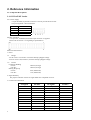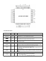
1
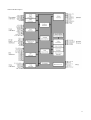
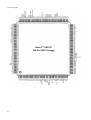
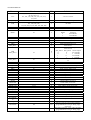
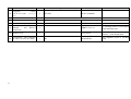
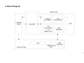
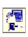
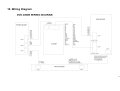
DVD PLAYER
DVG-4000N
SERVICE MANUAL
CONTENTS
1. PRECAUTIONS ----------------------------------------------------------------------------------------------------------------------------1
1-1 SAFETY PRECAUTIONS -----------------------------------------------------------------------------------------------------------------1
1-2 SERVICING PRECAUTIONS -------------------------------------------------------------------------------------------------------------2
1-2-1 General Serving Precautions ---------------------------------------------------------------------------------------------------2
1-2-2 Insulation Checking Procedure ------------------------------------------------------------------------------------------------3
1-3 ESD PRECAUTIONS---------------------------------------------------------------------------------------------------------------------3
2. REFERENCE INFORMATION ----------------------------------------------------------------------------------------------------------4
2-1 COMPONENT DESCRIPTIONS ----------------------------------------------------------------------------------------------------------4
2-1-1 DVD ATAPI Loader -------------------------------------------------------------------------------------------------------------4
2-1-2 NTSC/PAL Digital Video Encoder (AV3168)-------------------------------------------------------------------------------6
2-1-3 DVD Processor Chip (Swan-2TM ES4318)--------------------------------------------------------------------------------- 10
2-1-4 8-Pin, 24-Bit, 96kHz Stereo D/A CONVERTER (CS4338) ------------------------------------------------------------ 14
2-1-5 Serial EEPROM, 2K (256 x 8) (AT24C02/01) ---------------------------------------------------------------------------- 15
2-1-6 4-Megabit (512 x 8) FLASH RAM (MX29F040) ------------------------------------------------------------------------ 16
2-1-7 512K X 16 Bit X 2 Banks Synchronous DRAM (A43L0616)---------------------------------------------------------- 17
3. PRODUCT SPECIFICATIONS -------------------------------------------------------------------------------------------------------- 21
4. OPERATING INSTRUCTIONS ------------------------------------------------------------------------------------------------------- 22
4-1 BASIC CONNECTIONS ---------------------------------------------------------------------------------------------------------------- 22
4-2 SELECTING VIDEO MODE ---------------------------------------------------------------------------------------------------------- 22
4-3 SELECTING THE DESIRED DVD MENU ITEM -------------------------------------------------------------------------------------- 23
4-4 SELECTING THE DESIRED MP3 FOLDER ------------------------------------------------------------------------------------------- 23
4-5 SELECTING THE DESIRED MP3 TITLE ---------------------------------------------------------------------------------------------- 23
4-6 SEARCHING ---------------------------------------------------------------------------------------------------------------------------- 23
4-7 RESUME PLAY ------------------------------------------------------------------------------------------------------------------------- 23
4-10 SELECTING SUBTITLE LANGUAGE ------------------------------------------------------------------------------------------------ 24
4-11 SELECTING ANGLE ------------------------------------------------------------------------------------------------------------------ 24
5. DISASSEMBLY AND REASSEMBLY ---------------------------------------------------------------------------------------------- 25
6. TROUBLESHOOTING------------------------------------------------------------------------------------------------------------------ 26
7. ELECTRICAL PART LIST ------------------------------------------------------------------------------------------------------------- 27
8. BLOCK DIAGRAM---------------------------------------------------------------------------------------------------------------------- 35
9. CIRCUIT DIAGRAMS ------------------------------------------------------------------------------------------------------------------ 36
10. WIRING DIAGRAM ------------------------------------------------------------------------------------------------------------------- 47
1. Precautions
1-1 Safety Precautions
1) Before returning an instrument to the customer, always
make a safety check of the entire instrument, including, but
not limited to, the following items:
(1) Be sure that no built-in protective devices are defective
or have been defeated during servicing.
(1) Protective shields are provided to protect both the
technician and the customer. Correctly replace all
missing protective shields, including any remove for
servicing convenience.
(2) When reinstalling the chassis and/or other
assembly in the cabinet, be sure to put back in place
all protective devices, including, but not limited to,
nonmetallic control knobs, insulating fish papers,
adjustment and compartment covers/shields, and
isolation resistor/capacitor networks. Do not operate
this instrument or permit it to be operated without all
protective devices correctly installed and functioning.
(2) Be sure that there are no cabinet opening through which
adults or children might be able to insert their fingers
and contact a hazardous voltage. Such openings
include, but are not limited to, excessively wide
cabinet ventilation slots, and an improperly fitted
and/or incorrectly secured cabinet back cover.
(3) Leakage Current Hot Check-With the instrument
completely reassembled, plug the AC line cord
directly into a 120V AC outlet. (Do not use an
isolation transformer during this test.) Use a leakage
current tester or a metering system that complies with
American National Standards institute (ANSI) C101.1
Leakage.
Current for Appliances and underwriters Laboratories
(UL) 1270 (40.7). With the instrument’s AC switch
first in the ON position and then in the OFF position,
measure from a known earth ground (metal water pipe,
conduit, etc.) to all exposed metal parts of the
instrument (antennas, handle brackets, metal cabinets,
screwheads, metallic overlays, control shafts, etc.),
especially and exposed metal parts that offer an
electrical return path to the chassis.
Any current measured must not exceed 0.5mA.
Reverse the instrument power cord plug in the outlet
and repeat the test.
AC Leakage Test
Any measurements not within the limits specified
herein indicate a potential shock hazard that must be
eliminated before returning the instrument to the
customer.
(4) Insulation Resistance Test Cold Check-(1) Unplug the
power supply cord and connect a jumper wore
between the two prongs of the plug. (2) Turn on the
power switch of the instrument. (3) Measure the
resistance with an ohmmeter between the jumpered
AC plug and all exposed metallic cabinet parts on the
instrument, such as screwheads, antenna, control
shafts, handle brackets, etc. When an exposed
metallic part has a return path to the chassis, the
reading should be between 1 and 5.2 megohm. When
there is no return path to the chassis, the reading must
be infinite. If the reading is not within the limits
specified, there is the possibility of a shock hazard,
and the instrument must be re-pared and rechecked
before it is returned to the customer.
Insulation Resistance Test
2) Read and comply with all caution and safety related
1
notes non or inside the cabinet, or on the chassis.
3) Design Alteration Warning-Do not alter of add to the
mechanical or electrical design of this instrument.
Design alterations and additions, including but not
limited to, circuit modifications and the addition of
items such as auxiliary audio output connections,
might alter the safety characteristics of this instrument
and create a hazard to the user. Any design alterations
or additions will make you, the service, responsible
for personal injury or property damage resulting there
from.
4) Observe original lead dress. Take extra care to assure
correct lead dress in the following areas:
(1) near sharp edges, (2) near thermally hot parts (be
sure that leads and components do not touch
thermally hot parts), (3) the AC supply, (4) high
voltage, and (5) antenna wiring. Always inspect in all
areas for pinched, out-of-place, or frayed wiring. Do
not change spacing between a component and the
printed-circuit board, Check the AC power cord for
damage.
5) Components, parts, and/or wiring that appear to have
overheated or that are otherwise damaged should be
replaced with components, parts and/or wiring that
meet original specifications. Additionally determine
the cause of overheating and/or damage and, if
necessary, take corrective action to remove and
potential safety hazard.
6) Product Safety Notice-Some electrical and mechanical
parts have special safety-related characteristics which
are often not evident from visual inspection, nor can
the protection they give necessarily be obtained by
replacing them with components rated for higher
voltage, wattage, etc. Parts that have special safety
characteristics are identified by shading, an ( ) or a
( ) on schematics and parts lists. Use of a substitute
replacement that does not have the same safety
characteristics as the recommended replacement part
might created shock, fire and/or other hazards.
Product safety is under review continuously and new
instructions are issued whenever appropriate.
1-2 Servicing Precautions
CAUTION: Before servicing Instruments covered by this
service manual and its supplements, read and follow the
Safety Precautions section of this manual.
Note: If unforeseen circument create conflict between the
following servicing precautions and any of the safety
precautions, always follow the safety precautions.
Remember; Safety First
1-2-1 General Serving Precautions
(1) a. Always unplug the instrument’s AC power cord from
the AC power source before (1) removing or
reinstalling any component, circuit board, module or
any other instrument assembly. (2) disconnecting
any instrument electrical plug or other electrical
connection. (3) connecting a test substitute in
parallel with an electrolytic capacitor in the
instrument.
b. Do not defeat any plug/socket B+ voltage interlocks
with which instruments covered by this service
manual might be equipped.
c. Do not apply AC power to this instrument and/or any
of its electrical assemblies unless all solid-state
2
device heat sinks are correctly installed.
d. Always connect a test instrument’s ground lead to
the instrument chassis ground before connecting the
test instrument positive lead. Always remove the test
instrument ground lead last.
Note: Refer to the Safety Precautions section ground
lead last.
(2) The service precautions are indicated or printed on the
cabinet, chassis or components. When servicing,
follow the printed or indicated service precautions
and service materials.
(3) The components used in the unit have a specified flame
resistance and dielectric strength.
When replacing components, use components which
have the same ratings, by ( ) or by ( ) in the
circuit diagram are important for safety or for the
characteristics of the unit. Always replace them with
the exact replacement components.
(4) An insulation tube or tape is sometimes used and some
components are raised above the printed wiring board
for safety. The internal wiring is sometimes clamped
to prevent contact with heating components. Install
such elements as they were.
(5) After servicing, always check that the removed screws,
components, and wiring have been installed correctly
and that the portion around the serviced part has not
been damaged and so on. Further, check the insulation
between the blades of the attachment plus and
accessible conductive parts.
1-2-2 Insulation Checking Procedure
turn the power ON. Connect the insulation resistance meter
(500V) to the blades of the attachment plug. The insulation
resistance between each blade of the attachment plug and
accessible conductive parts (see note) should be more than
1 Megohm.
Note: Accessible conductive parts include metal panels,
input terminals, earphone jacks, etc.
Disconnect the attachment plug from the AC outlet and
1-3 ESD Precautions
Electrostatically Sensitive Devices (ESD)
Some semiconductor (solid static electricity) devices can
be damaged easily by static electricity.
Such compo9nents commonly are called Electrostatically
Sensitive Devices (ESD). Examples of typical ESD devices
are integrated circuits and some field-effect transistors and
semiconductor chip components. The following techniques
of component damage caused by static electricity.
(1) immediately before handling any semiconductor
components or semiconductor-equipped assembly,
drain off any electrostatic charge on your body by
touching a known earth ground. Alternatively, obtain
and wear a commercially available discharging wrist
strap device, which should be removed for potential
shock reasons prior to applying power to the unit
under test.
(2) after removing an electrical assembly equipped with
ESD devices, place the assembly on a conductive
surface such as aluminum foil, to prevent electrostatic
charge buildup or exposure of the assembly.
(3) Use only a grounded-tip soldering iron to solder or
unsolder ESD device.
(4) Use only an anti-static solder removal devices. Some
solder removal devices not classified as “anti-static”
can generate electrical charges sufficient to damage
ESD devices.
(5) Do not use freon-propelled chemicals. These can
generate electrical charges sufficient to damage ESD
devices.
(6) Do not remove a replacement ESD device from its
protective package until immediately before you are
ready to install it. (Most replacement ES devices are
packaged with leads electrically shorted together by
conductive foam, aluminum foil or comparable
conductive materials).
(7) Immediately before removing the protective materials
from the leads of a replacement ES device touch the
protective material to the chassis or circuit assembly
into which the device will be installed.
CAUTION: Be sure no power is applied to the chassis or
circuit, and observe all other safety precautions.
(8) Minimize bodily motions when handling unpackaged
replacement ESD devices. (Otherwise harmless
motion such as the brushing together of your clothes
fabric or the lifting of your foot from a carpeted floor
can generate static electricity sufficient to damage an
ESD device).
3
2. Reference Information
2-1 Component Descriptions
2-1-1 DVD ATAPI Loader
D.C. Power Supply
A 4-pin shrouded, keyed male connector is used to provide the D.C.Power.
The pin assignment is described below.
PIN
1
2
3
4
DC VOLTS
+12V
GND
GND
+5V
Interface Connector
A 39-pin male, unshielded, shrouded, keyed connector are applied.
Please refer to Section 7-2-3 regarding its pin definition.
Electrical Characteristics
1. Power
1-1. Voltage
+5V DC with ± 5% tolerance. Less than 100mVp-p Ripple Voltage
+12V DC with ± 10% tolerance, less than 150mVp-p Ripple Voltage
1-2. Current
Continuous Reading
+5V DC
+12V DC
Seeking & Spin up
+5V DC
+12V DC
500mA (Average)
300mA (Average)
0.8A (Maximum)
1.5A (Maximum)
2. Signal Summary
The physical interface consists of single ended TTL compatible receivers.
3. Connector Pin Definition
I/F Signals
4
I/O Pin #
I/F Signals
I/O Pin #
Reset
1
DMARQ
21
GND
2
GND
22
DD7
3
DIOW
23
DD8
4
GND
24
DD6
5
DIOR
25
DD9
6
GND
26
DD5
7
IORDY
27
DD10
8
CSEL
28
DD4
9
DMACK
29
DD11
10
GND
30
DD3
11
INTRQ
31
I/F Signals
I/O Pin #
I/F Signals
I/O Pin #
DD12
12
IOCS16
32
DD2
13
DA1
33
DD13
14
PDIAG
34
DD1
15
DA0
35
DD14
16
DA1
36
DD0
17
CS1FS
37
DD15
18
CS3FS
38
GND
19
DASP
39
NC
20
GND
40
4. Block Diagram
5
2-1-2 NTSC/PAL Digital Video Encoder (AV3168)
FEATURES
• Fully CCIR 624 performance compliance NTSC and
PAL (B,D,G,H,I,M and N) video encoder.
• Composite, S-video, Component Y/Cb/Cr (Sony,
Matsushita, and SMPTE) or RGB output.
• Triple 10-bit digital to analog converter.
• Accepts 27 Mhz multiplexed 8-bit digital video inputs.
• Master or Slave 4-Field NTSC or 8-Field PAL video
timing generation.
• CCIR 656 EAV SYNC extraction.
• Automatic NTSC or PAL timing detection in slave
mode operation.
• Automatic or User Programmable Chroma Filter
Selection.
• Macrovision Anti-Tapping Rev 7.01 support in
AV3168 Only.
• Closed Caption Support.
• Contrast and Brightness control.
Clock Generation
• 3 outputs for 27 MHz video clock, 16.934, 18.432 and
36.864 Mhz audio clock, and 40.5, 54.0, 67.5 and
81.0 MHz general purpose clocks.
• Requires a single 27 Mhz crystal.
General
• CVBS and S-video DAC power down controls.
• I2C compatible serial control bus.
• Single +5 volt power supply.
Application
• Digital Video Disk (DVD)
• Digital Set-Top Box
• PC Video, Multimedia
Ordering Information
AV3168/69-CL 44-pin PLCC
AV3168/69-CQ 44-pin TQFP
DESCRIPTION
The AV3168 is a mixed signal CMOS monolithic device. It comprise with a PAL and NTSC Video Encoder, Color
Space Converter and Clock Generator, The Clock Generator outputs a video, an audio and a programmable
general purpose clock. This IC implemented Macrovision Anti-tapping 7.01, intended for DVD and Settop Box
applications.
The video encoder converts CCIR 601 8-bit multiplexed digital video into RGB, component YCbCr, encoded NTSC
or PAL (BDGHIMN) signals. It contains three 10-bit DACs to support simultaneous S-video and composite video;
or component video display. Brightness and Contrast control are also provided.
6
The Clock Generator outputs three clocks for video, audio and system to simplify the system configuration and
maintain A/V synchronization.
Typical Application Connection
AV3168 Detailed Block Diagram
7
PIN DESCRIPTIONS
Pin Name
Pin #
Type
Description
DIGITAL VIDEO INPUT
PD<7 -0>
11-16
18-19
I
HSYN
20
I/O
VSYN
21
I/O
Multiplexed Cb, Y, and Cr digital video input bus.
In Slave Mode (MSTR pin is low) Horizontal Synch input. In Master
Mode (MSTR pin is high) Horizontal Synch output.
In slave mode (MSTR pin is low) Vertical Sync input. In master mode
Vertical Sync output.
VIDEO CONTROL SIGNALS
MSTR
3
I
CPNT
27
I
PDEN
28
1
Master Mode;
If this pin is high, the chip outputs horizontal and vertical sync signals.
Otherwise it receives both horizontal and vertical sync signals.
Select either component or composite video output.
0: Simultaneous Composite and S-Video output.
1: Component video output either RGB or YCbCr determined by the
register CR0[5:4].
Pedestal enable pins.
When this pin is high 7.5 IRE is added for the NTSC composite analog
output.
VIDEO ANALOG OUTPUT, REFERENCE AND COMPENSATION
CVBS
8
35
O
Analog video output
Determined by the state of CPNT pin and CR0[5:4]
CPNT CR0[5] CR0 [4]
0
X
X:
Composite video output
Pin Name
Pin #
Type
Y
31
O
C
33
O
VREF
40
I/O
IREF
39
I
COMP
38
I
BIAS
37
I/O
Description
1
X
0:
Cr output in CbCr component mode
1
0
X:
:
1
1
1:
Blue color output in RGB mode
Analog video output
Determined by the state of CPNT pin and CR0[5:4]
CPNT CR0[5] CR0 [4]
0
X
X:
S-Video Y output.
1
X
0:
Cb output in CbCr component mode
1
0
X:
:
1
1
1:
R color output in RGB mode
Analog video output
Determined by the state of CPNT pin and CR0[5:4]
CPNT CR0[5] CR0 [4]
0
X
X:
S-Video C output.
1
1
0:
Cb output in CbCr component mode
1
0
X:
:
1
1
X:
Green color output in RGB mode
Voltage reference. It has an internal voltage reference circuit, but may
be overridden by an external voltage reference input. A 0.1 uF ceramic
capacitor is required between this pin and GND.
A resistor should be connected between this pin and GND to control the
DAC output current. The recommended value is 198 (382) ohm 1%
metal film resistor for double (single) end 75 ohm termination.
Compensation capacitor for the DAC internal reference amplifier. A 0.1
uF ceramic capacitor is required between this pin and VDDA.
DAC bias voltage. A 0.1 uf ceramic capacitor must be used to
de-couple this pin to VDDA.
SERIALCONTRL BUS
SCL
24
I
SDA
23
I/0
Serial bus clock
Serial bus address and data input and output pin.
Open drain output.
CLOCK SIGNALS
General Purpose Clock. Clock frequency is determined by the state of
GCK
7
O
GCK
7
O
CK27
9
O
ACK
25
I/O
XIN
XOUT
2
1
I
O
GOUT[1:0] when RST pin is low.
0 0 : 40.5 MHz clock output.
0 1: 54.0 MHz clock output.
1 0: 67.5 Mhz clock output.
1 1: 81.0 MHz
General Purpose Clock. Clock frequency is determined by the state of
GOUT[1:0] when RST pin is low.
0 0 : 40.5 MHz clock output.
0 1: 54.0 MHz clock output.
1 0: 67.5 Mhz clock output.
1 1: 81.0 MHz
27 MHz clock output pin.
384*fs Audio clock output pin.
Controlled by CR2[1:0]
0 0: 384 * 44.1 KHz (16.934MHz) clock output.
0 1: 384 * 48.0 KHz (18.432MHz) clock output.
1 0: 384 * 88.2 KHz (33.868MHz) clock output.
1 1. 384 * 96.0 KHz (36.864MHz) clock output.
27 Mhz oscillator input
27 Mhz oscillator output
MISCELLANEOUS SIGNALS
RST
6
I
GOUT1
44
O
Active low chip reset input. Chip is in the power down mode when the
RST is low.
Dual function pin.
9
Pin Name
Pin #
Type
Description
GCK frequency select pin when
RST is low.
General purpose output pin when
RST is high
Dual function pin.
GOUT0
43
I
GCK frequency select pin when
pin when
RST is low. General purpose output
RST is high
POWER AND GROUND
VDD
10, 22,
5
+5V
Digital power supply
VSS
8, 17,
26, 30,
34, 41,
42, 4
GND
Digital ground
VDDA
29,
32,36
+5V
Analog video power supply
2-1-3 DVD Processor Chip (Swan-2TM ES4318)
* Features
Single-chip DVD video decoder in a 208-pin PQFP package
Supports MPEG-1 system and MPEG-2 program streams
Programmable multimedia processor architecture
Compatible with Audio CD, Video CD, VCD 3.0, and Super Video CD (SVCD)
DVD Navigation 1
Built-in content Scrambling System (CSS)
- Audio
Built-in Karaoke key-shift function
DolbyTM Digital 2-channel down mix audio output for DolbyTM
Dolby Pro Logic
Linear PCM streams for24 bit / 96KHz
Concurrent S/PDIF out and 2-channel audio output
Sensaura Dolby Digital Virtual Surround
DTS Digital Surround 2-channel down mix stereo output
S/PDIF output for encoded AC-3, DTS Digital output or Linear PCM
- Peripheral
Glueless interface to DVD loaders (ATAPI or A/V bus I/F)
Bi-directional 12C audio interface
8 general-purpose auxiliary ports
Single 27MHz clock input
- Smart Technology
SmartZoomTM for motion zoom & pan
10
SmartZoomTM
for NTSC to PAL conversion and vice versa
SmartZoomTM
for video error concealment
* Functional Description
11
* Pinout Diagram
12
* PIN DESCRIPTON
Name
Number
I/O
Definition
I
3.65 V ± 150 mv.
O
Device address output
I
Ground
I
O
71
74:72
96:93, 90:85, 82:77
97,100
101
102
105
115:113, 110:106
I/O
I/O
O
I
I
I
I
I
O
O
O
O
I
O
O
I/O
O
O
O
I
O
Reset input active low.
TDM transmit data
ROM Select
RSEL
Selection
0
16-bit ROM
1
8-bit ROM
TDM receive data.
TDM clock input.
TDM frame synch.
TDM output enable, active low.
Audio transmit frame sync.
Select PLL1.
Audio transmit serial data port.
Select PLL0.
SEL_PLL2 SEL_PLL0 Clock Output
0
0
2.5 x DCLK
0
1
3 x DCLK
1
0
3.5 x DCLK
1
1
4 x DCLK
Select PLL2. See the table for pin number
33.
Audio master clock for audio DAC.
Audio transmit bit clock.
S/PDIF (IEC958) Format Output.
Audio receive serial data.
Audio receive frame synch.
Audio receive bit clock.
Analog PLL Capacitor.
Crystal input.
Crystal output.
DRAM address bus.
Column address strobe, active low.
Output enable, active low.
Clock enable, active low.
DRAM write enable, active low.
Row address strobe, active low.
DRAM data bus.
SDRAM chip select [1:0], active low.
Data input/ output mask.
Clock to SDRAM.
Clock input (27MHz).
8-bit YUV output.
116
I/O
2X pixel clock.
117
I/O
VSYNCH#
118
I/O
HSYNCH#
119
I/O
Pixel clock.
Vertical synch for screen video interface,
programmable for rising or falling edge,
active low.
Horizontal synch for screen video interface,
programmable for rising or falling edge,
1, 9, 18, 27, 35, 44, 51, 59, 68, 75, 83,
92, 99, 104, 111,
121, 130, 139, 148, 157, 164, 172, 183,
193, 201
23:19, 16:10, 7:2, 207:204
8, 17, 26, 34, 43, 52, 60, 67, 76, 84, 91, 98, 103,
112, 120, 129, 138,
147,156,163,171,177,184, 192, 200, 208
24
RSEL
25
I
TDMDR
TDMCLK
TDMFS
TDMTSC#
TWS
SEL_PLL1
28
29
30
31
I
I
I
O
O
I
VCC
LA[21:0]
VSS
RESET#
TDMDX
32
TSD
SEL_PLL0
33
SEL_PLL2
36
MCLK
TBCK
SDIF_DOBM
RSD
RWS
RBCK
APLLCAP
XIN
XOUT
DMA[11:0]
DCAS#
DOE#
DSCK-EN
DWE#
DRAS[2.0]#
DB[15:0]
DCS[1:0]#
DQM
DSCK
DCLK
YUV[7.0]
PCLK2XSC
N
PCLKQSCN
39
40
41
45
46
47
48
49
50
66:61, 58:53
69
70
O
I
13
Name
Number
I/O
Definition
HD[15:0]
HCS1FX#
HCS3FX#
HIOCS16#
HA[2:0]
VPP
HWR#/DCI_
ACK#
HRD#DCI-C
LK
HD[15:0]
HWRQ#
HRDQ#
HIRQ
HRST#
HIORDY
HWR#
AUX[7:0]
LOE#
LCS[3:0]#
LD[15;0]
LWRLL#
LWRHL#
NC
141:140, 137:131, 128:122
152
153
151
158, 155:154
159
O
O
O
I
I/O
I
149
I,I
150
I,I
Host read/DCI Interface Clock.
141:140, 137:131, 128:122
142
143
144
145
146
149
169:165, 162:160
170
176:173
197:194, 191:185, 182:178
198
199
37, 38, 42, 203:202
I/O
O
O
I/O
O
I
O
I/O
O
O
I/O
O
O
Host data bus.
Host write request.
Host read request.
Host interrupt.
Host reset.
Host I/O ready.
Host write request.
Auxiliary ports.
Device output enable, active low.
Chip select[3.0], active low.
Device data bus.
Device write enable, active low.
Device write enable, active low.
No Connect pins. Leave open
active low.
Host data bus
Host select 1.
Host select 3.
Device 16-bit data transfer.
Host address bus.
Peripheral protection voltage.
Host write/DCI interface Acknowledge
Signal, active low.
2-1-4 8-Pin, 24-Bit, 96kHz Stereo D/A CONVERTER (CS4338)
Features
♦ Complete Stereo DAC System: Interpolation,
D/A, Output Analog Filtering
♦ 24-Bit Conversion
♦ 96 dB Dynamic Range
♦ -88 dB THD+N
♦ Low Clock Jitter Sensitivity
♦ Single +5 V Power Supply
♦ Filtered Line Level Outputs
♦ On-Chip Digital De-emphasis
®
♦ Popgaurd Technology
♦ Functionally Compatible with CS4330/31/33
Description
The CS4334 family members are complete, stereo
digital-to-analog output systems including
14
interpolation, 1-bit D/A conversion and output analog
filtering in an 8-pin package. The CS4334/5/6/7/8/9
support all major audio data interface formats, and
the individual devices differ only in the supported
interface format.
The CS4334 family is based on delta-sigma
modulation, where the modulator output controls the
reference voltage input to an ultra-linear analog
low-pass filter. This architecture allows for infinite
adjustment of sample rate between 2 kHz and 100
kHz simply by changing the master clock frequency.
The CS4334 family contains on-chip digital
de-emphasis, operates from a single +5V power
supply, and requires minimal support circuitry. These
features are ideal for set-top boxes, DVD players,
SVCD players, and A/V receivers.
PIN DESCRIPTIONS
2-1-5 Serial EEPROM, 2K (256 x 8) (AT24C02/01)
* Features
Low-Voltage and Standard-Voltage Operation
-5.0 (V CC = 4.5V to 5.5V)
-2.7 (V CC = 2.7V to 5.5V)
-2.5 (V CC = 2.5V to 5.5V)
-1.8 (V CC = 1.8V to 5.5V)
15
Internally Organized 128 x 8 (1K), 256 x 8 (2K), 512 x 8 (4K), 1024 x 8 (8K) or 2048 x 8 (16K)
2-Wire Serial Interface
Schmitt Trigger, Filtered Inputs for Noise Suppression
Bi-directional Data Transfer Protocol
100 kHz (1.8v, 2.5V, 2.7V) and 400 kHz (5V) Compatibility
Write Protect Pin for Hardware Data Protection
8-Byte Page (1K, 2K), 16-Byte Page (4K, 8K, 16K) Write Modes
Partial Page Writes Are Allowed
Self-Timed Write Cycle (10 ms max)
High Reliability
-
Endurance: 1 Million Write Cycles
-
Data Retention: 100 Years
-
ESD Protection: >3000V
Automotive Grade and Extended Temperature Devices Available
8-Pin and 14-Pin JEDEC SOIC, 8-Pin PDIP, 8-Pin MSOP, and 8-Pin TSSOP Packages
* Pin Configurations
* Pin Description
Pin Name
A0-A2
SDA
SCL
WP
NC
Function
Address Inputs
Serial Data
Serial Clock input
Write Protect
No Connect
2-1-6 4-Megabit (512 x 8) FLASH RAM (MX29F040)
* Features
Fast Read Access Time – 70 ns
Low power CMOS Operation
-100 µA max. Standby
-30 µA max. Active at 5 MHz
JEDEC Standard Packages
High Reliability CMOS Technology
-2000V ESD Protection
-200 mA Latchup Immunity
RapidTM Programming Algorithm – 100 µs/byte (typical)
CMOS and TTL Compatible Inputs and Outputs
16
Integrated Product Identification Code
Commercial and Industrial Temperature Ranges
* Pin Configurations
* Pin Description
Pin Name
A0 – A18
O0 – O7
CE#
OE#
Function
Addresses
Outputs
Chip Enable
Output Enable
* Absolute Maximum Ratings
Temperature Under Bias………………………….-55oC to + 125 oC
Storage Temperature……………………………...-65 oC to + 150 oC
Voltage on Any Pin with Respect to Ground……..-2.0V to + 7.0V
Voltage on A9 with Respect to Ground…………...-2.0V to + 14.0V
V PP Supply Voltage with Respect to Ground…….-2.0V to + 14.0V
2-1-7 512K X 16 Bit X 2 Banks Synchronous DRAM (A43L0616)
Features
JEDEC standard 3.3V power supply
LVTTL compatible with multiplexed address
Dual banks / Pulse RAS
MRS cycle with address key programs
-
CAS Latency (2,3)
-
Burst Length (1,2,4,8 & full page)
-
Burst Type (Sequential & interleave)
17
All inputs are sampled at the positive going edge of the system clock
Burst Read Single-bit Write operation
DQM for masking
Auto & self refresh
64ms refresh period (4K cycle)
50 Pin TSOP (II)
Pin Configuration
18
Block Diagram
Pin Descriptions
Symbol
Name
CLk
System Clock
CS
Chip Select
Description
Active on the positive going edge to sample all inputs
Disables or Enables device operation by masking or enabling
all inputs except CLK, CKE and L(U)DQM
Masks system clock to freeze operation from the next clock cycle.
CKE
Clock Enable
A0~A10/AP
Address
BA
Bank Select Address
RAS
Row address Strobe
CAS
Column Address Strobe
WE
Write Enable
CKE should be enabled at least one clock + tss prior to new command.
Disable input buffers for power down in standby.
Row/Column addresses are multiplexed on the same pins.
Row address: RA0 ~ RA10, Column address: CA0 ~ CA7
Selects bank to be activated during row address latch time.
Selects band for read/write during column address latch time.
Latches row addresses on the positive going edge of the CLK with
RAS low.
Enables row access & precharge.
Latches column addresses on the positive going edge of the CLK with CAS
low. Enables column access.
Enables write operation and Row precharge.
19
Symbol
Name
L(U)DQM
Data Input/Output Mask
DW0-15
Data Input/Output
VDD/VSS
VDDQ/VSSQ
Power Supply/Ground
Data Output
Power/Ground
NC/RFU
No Connection
20
Description
Makes data output Hi-Z, t SHZ after the clock and masks the output.
Blocks data input when L(U)DQM active.
Data inputs/outputs are multiplexed on the same pins.
Power Supply: +3.3V±0.3V/Ground
Provide isolated Power/Ground to DQs for improved noise immunity.
3. Product Specifications
Playback System
DVD Video
Video CD (1.1, 2.0, 3.0)
SVCD and CVD
CDDA
CD-ROM with MP3 data
Television Signal System
NTSC/PAL
Video Performance
Video Out
1 Vpp into 75 ohm
S-Video Out
Y: 1Vpp into 75 ohm
C: 0.286 Vpp into 75 ohm
Component Out
0.7 Vpp into 75 ohm
D/A Converter
27MHz/10bit
Audio Performance
Frequency Response
DVD: fs 48/96KHz, 4Hz~22/44KHz
Video CD: fs 44.1KHz, 4Hz~20KHz
Audio CD: fs 44.1KHz, 4Hz~20KHz
Output Level
Analog: 2Vrms(1KHZ)
Digital: 1.15 Vpp
D/A Converter
96KHz/24bit
S/N Ratio
90dB
Connections
Coaxial digital out
Audio Analog out for 2-channel
Composite Video out
S-Video out
Power Supply
Power Source
Power Consumption
Set
Dimensions (W X H X D)
Net Weight
Gross Weight
X1
X1
X1
X1
AC100~240V, 50/60Hz
<25 Watt
495 X 155 X 348 (mm)
4.0 Kg
4.5 Kg
21
4. Operating Instructions
4-1 Basic Connections
* CONNECTED TO A TV
* CONNECTED TO AN ORDINARY AMPLIFIER
R
L
4-2 Selecting Video MODE
Press SETUP button and select GENERAL SETUP submenu on SETUP screen. After that, select TV TYPE by
pressing DOWN arrow button (▼ ) until desired TV mode is selected. For more information, refer to Page 34-36 on
the Instruction Manual.
22
4-3 Selecting the desired DVD menu Item
Some DVDs have title menus and chapter menus. Press MENU or TITLE,the
screen shows the menu.Then use direction buttons to select the desired item,press PLAY.
4-4 Selecting the desired MP3 folder
Use arrow button to select the folder you want to play. Then by pressing the PLAY button ,you can see the
the file lists under the folder.
Example:
Press the PLAY button
4-5 Selecting the desired MP3 title
Use arrow button and select an MP3 title using the PLAY button then play will start automatically. When you know
the title number, enter the MP3 title number using numeric buttons on the remoter control and press the PLAY button. If you
want to play an adjacent MP3 title, press the NEXT button for next title and the PREV button for previous title during
playing. To select “005 HAVEYOU” MP3 title in this case, press the DOWN arrow button twice and press the PLAY
button.
Example:
1.
Press the DOWN arrow button ( ▼ )
2.
Press the DOWN arrow button ( ▼ )
3.
Press the SELECT button
4-6 Searching
When you want to view the disc contents in fast farward or fast reverse, you can do that by pressing FF button ( ) or
FR button (). When playing DVD,there are five choices for both directions:FAST2X, FAST4X, FAST8X, FAST16X
FAST32X.When playing SUPER-VCD or VCD, four choices for both directions:FAST1X, :FAST2X, :FAST3X, :FAST4X.
When playing CD.MP3,press to play forward fast and to reverse the disc.
4-7 Resume Play
The unit can memorize the last point where it stops and resume playback from there. While playing
CD,MP3,press STOP to stop playing and then press MEMORY to resume playback. However, this function does not
work for any programmed playback ;it is removed when the disc is unloaded or the unit is off.
23
4-8 Slow Viewing
When you want to view the disc contents very slowly in forward or reverse direction, you can do that by pressing the
SLOW button. When playing DVD,there are six choices:SF2X, SF4X, SF8X, SR2X, SR4X, SR8X. While playing
SUPER-VCD OR VCD,there are three choices: SF1x, SF2x, SF3x.Take DVD for example, to view at slow 2x in
reverse direction ,press the slow buttom four times. To resume playing normally ,just press PLAY.
4-9 Selecting Audio Language
This function works only with discs on which multiple audio sound track languages are recorded. If the loaded disc
supports multiple languages, you can see the AUD indicator on fluorescent display. IN the figure shown right, there are total
8 audio languages. To select the third audio language, press the AUDIO button twice during play.
Example:
1.
Press the AUDIO button
2.
Press the AUDIO button
4-10 Selecting Subtitle Language
This function works only with discs on which multiple subtitle languages are recorded. If the loaded disc supports
multiple languages, you can see the SUB-T indicator on fluorescent display, In the figure shown right, there is only one
subtitle language. To turn on the subtitle language, press the SUBTITLE button. If you press it again, you can turn off the
subtitle language.
Example:
1.
Press the SUBTITLE button
4-11 Selecting Angle
Some DVD discs may contain scenes, which have shot simultaneously from a number of different angles. If the loaded
disc supports multiple angles, you can see indicator on the fluorescent display and the TV screen. In the figure shown right,
there are total 4 angles. To switch to the angle number2, press the ANGLE button.
24
5. Disassembly and Reassembly
25
6. Troubleshooting
No power
No picture
No sound
Distorted sound
Insert the AC power plug securely into the power outlet.
Make sure that the equipment is connected properly.
Make sure that the input setting for TV is Video (AV).
Make sure that the equipment is connected properly.
Make sure that the input settings for the TV and stereo system are correct.
No fast forward or fast reverse
Some discs may have sections that prohibit fast forward or fast reverse.
No proper aspect ratio
Select the correct setup for TV aspect ratio that matches your TV set.
Check the batteries are installed with the correct polarities.
No operations can be performed with Point the remote control unit at the remote control sensor and operate.
Remove the obstacles between the remote control unit and remote control
the remote controller
sensor.
Set the POWER button to OFF and then back to ON.
No button operation
Alternatively, turn off the power, disconnect the power plug and then
reconnect it.
If the audio soundtrack and /or subtitle language does not exist on the
Audio soundtrack and/or Subtitle disc, the language selected at the initial settings will not be seen.
language is not the one you selected.
This function is dependent on software availability. Even if a disc has a
No Angle change
number of angles recorded, these angles may be recorded for specific
scenes only.
26
7. Electrical Part List
DVG-4000N PRODUCT DESIGN PACKAGE LIST
No.
Name
Counts
Blueprint No.
Material No.
Notes
1
DVG4000N surface subassembly
1
BC-PMGDVG3000N
2
HPT DVD machine core
1
JX-HPTAM-2266
3
bracket of machine core
2
WJ-JXZJ930E5
the height of HPT machine core:17.5mm
4
DAYU
DVD
two-channel
decoding subassembly
1
GV-DJH930
BC-PDJH930-01
with phone output
5
GV-DPA868 subassembly
1
GV-DPA868
BC-PDPA86802
10/20/2k
6
motherboard
1
GV-DZ930E2-03
WJ-DZ930E2-03
silver gray,use electrolyzed iron
7
backboard
1
GV-HB3000N-01
WJ-HBDVG3000N
8
outer cover
1
GV-WZ3000N
WJ-WZ3000N
9
wire of power-supply
1
DY-1M8LYTWKUL
black, two-head, both-insulated ,polar,with UL
certificate
10
PE bag of power-supply wire
1
BZ-JDDYX-01
unit
80*160mm
environment-protecting
the
number
of
paper:GV-HB3000N-01SY
with mark DAEWOO
5
FJ-FJNLZX
12
尼 龙 带 扎 线 fastening string
made of nylon ribbon
black fastening string
1
FJ-FJHZX
for power-supply wire
13
magnetic ring
1
CH-281675
outer diameter
16mm
11
28mm
with
silk-screen
mark
of
inter diameter
height 7.5mm
27
No.
Counts
Blueprint No.
Material No.
Notes
14
MIC shielded sheet iron
1
GV-MICPBZ930-01
WJ-MICPBZ930
15
930B CD gate-bar
1
GV-CDM930HPT-01
SJ-CDM930HPT
for HPT machine core
16
DVD paster for trademark
1
SJ-DVDSBP
with background black and characters silvery
17
strut for circuit board
8
SJ-XLBJZ-01(新)
decodeing board 2
power-supply board 6
18
plastic nut cap
8
SJ-XLBJZ-02(新)
decodeing board 2
power-supply board 6
19
970 rubber tray
2
SJ-VCDJJD2MM
20
VCD rubber tray
3
SJ-VCDJJD5MM
21
remote control unit
1
22
battery
23
PE bag for remote control unit
24
BZ-YKQDVG3000N
BZ-YKQDVG3000N
BZ-YKQDVG3000N-01 BZ-YKQDVG3000N-01
thickness 2mm
diameter 10mm
thickness 5mm diameter 50mm
black ENGLISH,for black DVG3000N
gray ENGLISH,for silvery DVG3000N
FJ-DC7#04
7# environment-protecting Hg-Ca battery
ENGLISH
1
BZ-JDYKQ-03
unit
manual
1
BZ-SMSDVG-3000N
英文
25
PE bag for remote control unit
1
BZ-JDYKQ-03
unit 05*80*260mm with
environment-protecting mark
26
foam
BZ-PMDVD-03(新)
340*143*65
27
handle of colourful box
1
28
colourful box
1
29
28
Name
pearl cotton 480*580
1对
1套
1
GV-PMDVD-03
05
80*260mm
BZ-CHTS-01
GV-CHDVG3000N-01
BZ-CHDVG3000N
FJ-ZZMD-02
unit
mm with environment-protecting mark
No.
Name
Counts
Blueprint No.
Material No.
Notes
30
nail BTV3*10 colouful zinc
4
LD-BTPW3*10C
machine core 4
31
with-cap hardened nailBTPW3*8
colorful zinc
8
LD-BTPW3*8C
outer cover 4
32
round-headed
self-fastened
hardened nailBTV3*6 colorful
zinc
12
LD-BTV3*6C
backboard 3, outer cover 4, side cover 2, cover
and motherboard 3
33
round-headed
self-fastened
hardened nailBTV3*16
colorful zinc
8
LD-BTV3*16C
power-supply board 6
34
plain-headed
colorful zinc
2
LD-BB3*8C
optical fiber
35
acute-headed nail BA3*8 colorful
zinc
1
LD-BA3*8C
same-axis output board
36
tooth-shaped BBM3*8 colorful
zinc
2
LD-BBM3*8
37
M diameter 3mm nut
2
LD-M3
mental shielding 2
38
video two-terminator
wire 1.5mm
1
DY-XSPLTLHX
linear figure,black
39
audio four-terminator red-white
1.5mm
1
DY-XYPSTLHX
linear figure,black
40
bar code
FJ-TZTXMDVG3000N
provided by client
41
assembly line number
FJ-LSHDVG3000N
provided by client
42
warranty card
1
BZ-BYZDVG3000N
ENGLISH, designed by client
43
2.54 connector /2.54 connector
40Pgray row-wire 250mm
1
PX-B250B40H
from decoding board to
44
2.54 connector 4P 130mm 5.0
head colorful wire
1
PX-F130B4C01
triangular
nail
yellow
machine cover 4
decoding board 2
audil output board
mental shielding 2
machine core
from power-supply board to machine core
29
No.
Name
Counts
45
2.54 connector/2.54connctor 6P
red-white row-wire 260mm
1
Blueprint No.
Material No.
Notes
from power-supply
board
PX-B260B6R
board to
The list for cover subassembly design of DVG4000N
No.
30
Name
Counts
Blueprint No.
Material No.
1
trademark
1
GV-SBPDAEWOO
WJ-SBPHDYZDAEWOO
2
DVG3000N panel
1
GV-MB930
SJ-MB3000N
3
DV930 power-supply button
1
GV-DYN930-01
SJ-DYN930
4
GV320S knob
2
GV-DWQXN320-01
SJ-XN320
5
number button
1
GV-SZN930-01
SJ-SZN930
6
fast forward button
1
GV-KJN930-01
SJ-KJN930
7
pause button
2
GV-ZTN930-01
SJ-ZTN930
8
load/unload button
1
GV-CHN930-01
SJ-CHN930
9
light-transporting canister
1
GV-DGT920
SJ-DGT920
10
930LCD screen lens
1
GV-XSJ3000N-01
SJ-XSTJ3000N
11
the left bracket for 550 panel
1
WJ-MBCZJZ550
12
the right bracket for 550 panel
1
WJ-MBCZJY550
13
the subassembly of 930 crystal control
pannel
1
BC-PDCA930L-01
14
the subassembly of DHB910 earphone
board
1
BC-PDHB910-01
15
aluminium bar
2
WJ-LJT
Notes
DAEWOO
silk-screen blueprint No.:
GV-MB3000N-01
silk-screen blueprint No.:
GV-XSTJ3000N-01
front foot(0.3*5*18)
decoding
No.
Name
Counts
Blueprint No.
Material No.
16
plain-headed triangular nail BB3*8
colorful zinc
16
LD-BB3*8C
17
power-supply cover
1
SJ-DYG
18
safety pasting-paper
1
FL-ACTZ
19
ordinary green round-headed LED
1
FG-3MMBFLGL
Notes
control panel 9 bracket for cover 4
microphone board 1
power-supply
switch 2
diameter: 3mm round-headed
The components design list for control panel
No.
Name/Specification
Counts
Position in the paper
Material No.
Notes
resistor
1
resistor 220E
2
resistor 47E
1/4W
10%
1
R1
DZ-RT220EYS
1
R2
DZ-RT47EYS
2
C3,C4
CC-271Y505
1
C1
CC-104Y505
diameter: 5mm
1
C2
CD-47W165
diameter:5mm
infrared-emitting diode
1
L1
EJ-HXFSEJG5MM
triode 9014
1
Q1
MD-9014350-700
oscillator 455E
1
X1
JJ-Z455E
1/4W
10%
porcelain capacitor
3
porcelain capacitor 270P
4
porcelain capacitor 104
50V -20%~+80%
electrolyzed
5
50V
20%
diameter:5mm
capacitor
electrolyzed capacitor 47UF
16V
diode
6
diameter:5mm,E,B,C PACKAGE
triode
7
350~700
oscillator
8
31
No.
Name/Specification
Counts
Position in the paper
Material No.
Notes
IC
9
IC
HT6221/M21-001
10
LCD screen-driving bounded IC
1
IC2
1
IC-HT6221
IC-LCDQDBD
M209A/DICLDRY
accessories
32
11
LCD screen
1
IC2
XS-PLCD
12
the background light of LCD screen
1
13
control panel
1
GV-DCB930L
PCBDKZB930-02
2001-5-5
14
touching-softly switch
25
K1~K25
KG-QCKG6*6*5-01
6*6*5
15
remote control receiver
1
JS-TRM8310
IRM8310
16
power switch
1
KG-DYKG01
TV-5 KDC-A10-1D 8A/128A 交流 250V
17
2.54connector
2P
without-terminator
red-white row-wire 260mm
1
RX-B260W2R
from control board to power-supply board
18
2.54 connector 6P red-white row-wire
280mm
1
RX-B280W6R01
from control board to decoding board
19
no-terminator 6P 2.0 gray row-wire 60mm
1
PX-W60W6H
from control board to LCDIC board
20
3.96connector 2P no-terminator 150 red
both-insulated
1
PX-E150W3R01
from switch board to power-supply board
21
iron thread 8mm
1
J1,J3,J4
FJ-TX8MM
diameter:0.6mm
22
iron thread 10mm
1
J2
FJ-TX10MM
diameter:]0.6mm
23
magnetic circle
1
CH-22513864
outer diameter 22.5mm inner diameter
13.8mm height 6.4mm
FJ-LCDBDJ
needed power-supply:4.4V
The component design list for DV-910 earphone board
No.
Name
Counts
resistor
resistor
10E
1/4W
1
10%
2 resistor
1K 1/4W
10%
resistor
4.7K
1/4W
3
10%
resistor
5.1K
1/4W
4
10%
5
100K 1/4W 10%
resistor
22K 1/4W
6
10%
resistor
47K
1/4W
7
10%
porcelain capacitor
porcelain capacitor
101
8
50V 10%
electrolyzed capacitor
9
electrolyzed
16V 20%
capacitor
10UF
10
electrolyzed capacitor 100UF
16V 20%
Blueprint No.
Material No.
Notes
4
R1,R2,R8,R9
DZ-RT10EYS
2
R21,R22
DZ-RT1KYS
5
R4,R6,R7,R12,R13
DZ-RT4K7YS
5
R10,R15,R16,R23,R24
DZ-RT5K1YS
2
R17,R18
DZ-RT100KYS
2
R19,R20
DZ-RT33KYS
4
R3,R5,R11,R14
DZ-RT47KYS
4
C3,C4,C9,C11
CC-101Y505
12
C1,C2,C6,C7,C8,C10,C13,C14,C15,C16,C17,C18 CD-10UW165
diameter:5mm
2
C5,C12
CD-101W165
diameter:5mm
2
IC1,IC2
IC-4558
2
Q1
MD-2SC1815350-650
2
MIC1
diameter:5mm
IC
11 IC
JRC4558
triode
12 triode 2SC1815
Q2
β=350~650
accessories
13
inserting hole for microphone
silvery side four-foot mode
MIC2
CZ-HTCK03
33
No.
Name
changeable
14 R1216G11A2-A20K
mode
15 PCB GV-DHB910
16 jumper
Counts
resistor
six-foot
10mm
2
Blueprint No.
RW1,RW2
1
3
J1,J2,J3
Material No.
Notes
DW-WT1Z20KS01
PCBDHB910
2001.04.28
FJ-TX10MM
diameter:0.6mm
17 bracket for microphone board
round-headed
self-fastened
18 hardened
nail BTV3*6
colorful zinc
1
WJMBZJ320
1
LDBBTV3*6C.A1
for fastening bracket of microphone
board and PCB board
19 magnetic circle
1
WJ-CH16128
outer
diameter:16mm
diameter : 12mm height:8mm
PX-B270W4R
from earphone board to decoding
board
20
34
2.54connector with terminator
red-white row-wire 4P 270mm
1
XH1
inner
8. Block Diagram
35
9. Circuit Diagrams
1. Control Part
2. Ear Part
3. Video Part
4. Clock Part
5. Memory Part
6. Chip 4318
7. D/A Converter Part
8. Atapi Part
9. Audio Part
10. Power Part
36
1
2
3
4
5
6
D
D
IC1
HT6221
1
2
3
4
5
6
7
8
9
10
C2
C1
100u/16V 104
L1
LED
X1
455E
CZ2
1
2
3
4
5
6
+5V
IR
GND
CLK
CS
DATA
VCC
SIG
GND
C3
271
Q1
9014
K10
KEY
K6
KEY
K5
KEY
K11
KEY
K14
KEY
K9
KEY
K8
KEY
K7
KEY
K13
KEY
K12
KEY
K22
KEY
K21
KEY
C4
271
K17
KEY
R2
47E
6PIN
C
20
19
18
17
16
15
14
13
12
11
3
2
1
C
K4
KEY
K3
KEY
K16
KEY
K15
KEY
K24
KEY
K19
KEY
K2
KEY
K1
KEY
K18
KEY
K20
KEY
K25
KEY
K23
KEY
+5V
REMOTE
REM
CZ3
1
+4.4V
2
2P
LED1
+
-
1
2
3
4
5
6
7
8
9
10
11
12
13
14
15
16
17
18
19
20
21
22
23
B
LEDIC
6
5
4
3
2
1
P1
P2
P3
P4
P5
P6
P7
P8
P9
P10
P11
P12
P13
P14
P15
P16
P17
P18
P19
P20
P21
P22
P23
7
8
9
10
11
12
13
14
15
16
17
CZ1
29
28
27
26
25
24
+5V
IR
GND
CLK
CS
DATA
1
2
3
4
5
6
+5V
R1
220E
LED
6PIN
18
19
20
21
22
23
B
24
A
25
A
+8V
1
2
3
4
5
6
2
3
C7
10uF
R4
4.7K
4
4
1
IC1A
UJM4558
2
C2
10uF
1
R2
10E
3
D
D
C4
100pF
8
1/2VCC
VCC
VCC
C18
10uF
XH1
C
4
3
2
1
VCC
4P2D54
R19
22K
R21
1K
7
1/2VCC
R1
10E
6
C6
10uF
C3
100pF
C16
10uF
R24
5.1K
R18
100K
C1
10uF
5
R6
4.7K
Q2
C1815
R20
22K
MIC1
CK-6.35-305
IC1B
UJM4558
R16
5.1K
VCC
+12V
GND
Rin
Lin
R5
47K
RW1
RD902G-BA1-A20K
R17
100K
C
R3
47K
R18
5.1K
C13
10uF
R12
4.7K
IC2B
UJM4558
5
MIC2
CK-6.35-305
C10
10uF
7
R9
10E
6
C17
10uF
R22
1K
+12V
R23
5.1K
Q1
C1815
C9
100pF
C15
10uF
C12
100uF
R7
4.7K
1/2VCC
VCC
1/2VCC
R11
47K
4
B
RW2
RD902G-BA1-A20K
R13
4.7K
2
1
C8
10uF
R8
10E
C5
100uF
R10
5.1K
B
3
8
C14
10uF
IC2A
UJM4558
R14
47K
C11
100pF
A
A
1
2
3
4
1
2
3
VVCC
4
TVCC
FB5
FERRITE BEAD
+5V
VVCC
FB1
FERRITE BEAD
+
C73
47uF
D
C60
0.1uF
C70
0.1uF
D
+
C89
100uF
C68
0.1uF
C65
22pF
L2
4.7uH
C67
10pF
C66
22pF
XH1
27.0000MHz
R106
100k
TVCC
C61
22pF
SW1D
AV6
CR/B
VVCC
6
5
4
3
2
1
44
43
42
41
40
R92
200
Q1
9014
1K(open)
7
8
9
10
11
12
13
14
15
16
17
U9
AV3168/9
D6
IN4148
C58
180pF
C62
180pF
C54
IREF
COMP
BIAS
VDDA
CVBS
VSS
C
VDDA
Y
VSS
VDDA
39
38
37
36
35
34
33
32
31
30
29
C
0.1uF
TVCC
C56
C63
22pF
0.1uF
D10
IN4148
R104
75 (1%)
D11
IN4148
L4
1.8uH
SW1F
AV6
C59
180pF
C92
180pF
PD6
PD7
VSYN
HSYN
VDD
SCD
SCL
ACK
VSS
CPNT
PDEN
27MHz
GCK
VSS
CK27
VDD
PD0
PD1
PD2
PD3
PD4
PD5
VSS
R123
75 (1%)
TVCC
Y/G
9
CB/R
8
10
R103
SW1C
AV6
4
5
1K
CVBS/Cr/B
J1
S-JACK
2
1
R102
AUX5
C
L1
1.8uH
C75
0.1uF
R105
4.7k
RST
VDD
VSS
MSTR
XIN
XOUT
GOUT1
GOUT0
VSS
VSS
VREF
R107
10k(OPEN)
6
7
D5
IN4148
5
D8
IN4148
YUV[0..7]
3
4
C55
22pF
18
19
20
21
22
23
24
25
26
27
28
TVCC
L3
1.8uH
SW1E
AV6
VSYNC
HSYNC
R98
75 (1%)
D9
IN4148
C53
180pF
C99
180pF
7
VVCC
B
B
AUX0
AUX1
R61
0
AUX3
R94
4.7K(OPEN)
VCCA
FB7
FERRITE BEAD
+
C28
47uF
VVCC
C21
0.1uF
J2
C39
0.1uF
AUX3
B
G
R
ROUT
LOUT
+12V
A
1
2
3
4
5
6
7
8
9
10
11
12
A
CON12
C39
0.1uF
Title
Size
Number
Revision
B
Date:
File:
1
2
3
14-Jul-2001
Sheet of
C:\product\backup\zjh\930F\930F2DVDSCH.DDB
Drawn By:
4
1
2
R151
3
(OPEN)
4
VCC
C145
10U/16V
R169
330E
R168
10K
D
R150
0 OHM
R59
27M
D
RST#
Q5
JE9014
33 OHM
DCLK
D7
1N4148
R170
10K
OPEN
E2
C22
OPEN
LFA30-2A1E473MB
U16
1
2
3
4
5
(15PF)
VCC
33 OHM
R64
NC
GND
NC
RES
VDD
XIN
V6300
Package: SOT-23 5L
No need if using CAT24C021
C24
OPEN
E4
LFA30-2A1E473MB
(15PF)
VCC
C
C
R63
R137
4.7K(OPEN)
33 OHM
AUX3
AUX3R61
E3
C25
15PF
LFA30-2A1E473MB
0
R57
33 OHM
R99
33 OHM
R52
33 OHM
TBCK
TBCK-
TWS
TWS-
TSD0
R81
TSD0-
33 OHM
PCLK2X
E1
B
C38
OPEN
LFA30-2A1E473MB
B
(15PF)
R68
33 OHM
R67
1717XI
E5
AUDCLK
E6
C41
OPEN
LFA30-2A1E473MB
220 OHM
MCLK
C30
OPEN
LFA30-2A1E473MB
(15PF)
(15PF)
930E2解码板PCB图
GVG
COMPANY
A
TITLE
GV-DJB930E2.SCH
FILE
A
SCALE:
REV:
00-11-25
SHEET:
Title
DESIGN
SHEET
OF
DRAWN BY
Size
DATE
CHECKED BY
Number
Date:
File:
1
2
3
APPROVED BY
Revision
B
14-Jul-2001
Sheet of
C:\product\backup\zjh\930F\930F2DVDSCH.DDB
Drawn By:
4
B/0
1
DMA[0..11]
2
R77
DMA0
VCC3
MA0
10 OHM
R90
DMA1
R89
MA1
MA1
MA2
MA3
MA2
MA4
MA5
10 OHM
R76
DMA3
D
MA6
MA3
MA7
MA8
10 OHM
R88
DMA4
MA9
MA4
MA10
MA11
10 OHM
R75
DMA5
MA5
10 OHM
R87
DMA6
R91
10 OHM
MA6
R74
R86
34
C46
OPEN
MA7
R73
MA9
10 OHM
R85
DMA10
RAS0#
17
CAS#
16
WE#
15
DQMX
14
MA8
10 OHM
DMA9
18
CS0#
(15PF)
10 OHM
DMA8
35
DSCK
10 OHM
DMA7
21
22
23
24
27
28
29
30
31
32
20
19
MA0
10 OHM
DMA2
3
MA10
36
10 OHM
R84
DMA11
33
37
VCC3
VCC3
A0
A1
A2
A3
A4
A5
A6
A7
A8
A9
A10
BA/A11
DQ0
DQ1
DQ2
DQ3
DQ4
DQ5
DQ6
DQ7
DQ8
DQ9
DQ10
DQ11
DQ12
DQ13
DQ14
DQ15
CLK
2
3
5
6
8
9
11
12
39
40
42
43
45
46
48
49
DB7
VCC
VCC
CS
RAS
VCCQ
VCCQ
VCCQ
VCCQ
CAS
MA0
DB[0..15]
MA1
DB6
MA2
DB5
MA3
DB4
MA4
DB3
MA5
DB2
MA6
DB1
MA7
DB0
MA8
DB8
MA9
DB9
MA10
DB10
MA11
DB12
R82
DB13
35
DSCK
DB14
10 OHM
DB15
34
C42
OPEN
1
25
VSSQ
VSSQ
VSSQ
VSSQ
DQMH
NC
NC
VSS
VSS
CS1#
18
RAS0#
17
CAS#
16
WE#
15
DQMX
14
(15PF)
7
13
38
44
WE
DQML
21
22
23
24
27
28
29
30
31
32
20
19
DB11
CKE
MA11
10 OHM
4
U3
VCC3
U2
4
10
41
47
36
33
37
26
50
A0
A1
A2
A3
A4
A5
A6
A7
A8
A9
A10
BA/A11
DQ0
DQ1
DQ2
DQ3
DQ4
DQ5
DQ6
DQ7
DQ8
DQ9
DQ10
DQ11
DQ12
DQ13
DQ14
DQ15
CLK
2
3
5
6
8
9
11
12
39
40
42
43
45
46
48
49
DB7
DB6
DB5
DB4
DB3
DB2
DB1
DB0
DB8
DB9
DB11
DB12
DB13
DB14
DB15
CKE
VCC
VCC
CS
RAS
VCCQ
VCCQ
VCCQ
VCCQ
CAS
1
25
7
13
38
44
WE
DQML
VSSQ
VSSQ
VSSQ
VSSQ
DQMH
NC
NC
VSS
VSS
4
10
41
47
26
50
SDRAM 512KX16X2 (9ns)
C
R78
C
SDRAM 512KX16X2 (9ns)
CS0#
DCS0#
D
DB10
33 OHM
R70
CS1#
DCS1#
33 OHM
U7
LD15
3
4
7
8
13
14
17
18
WR2
1
11
LD8
R71
RAS0#
DRAS0#
LD9
LD10
33 OHM
LD11
LD12
R72
CAS#
DCAS#
LD13
LD14
33 OHM
R83
WE#
DWE#
33 OHM
LCS2#
R69
Q0
Q1
Q2
Q3
Q4
Q5
Q6
Q7
2
5
6
9
12
15
16
19
YSS-CS
YSS-CS
YSS-CLK
YSS-CDI
MC
ML
MD
AUDRST#
YSS-CLK
YSS-CDI
MC
ML
MD
AUDRST#
OC
CLK
74F374
DQMX
DQM
D0
D1
D2
D3
D4
D5
D6
D7
33 OHM
U4
LA[0..19]
LA0
LA1
B
LA2
LA3
LA4
LA5
LA6
LA7
LA8
OPEN
R41
LA9
LA18
LA18
LA10
LA19
LA11
LA12
CRITICAL TRACES
LA13
WRLL#
MOST
CLOCKS
LA14
R42
LA15
LA16
(0 OHM)
LA17
ADDRESS
OPEN
R46
CAS
WE
LCS3#
LOE#
LA19
LOE#
12
11
10
9
8
7
6
5
27
26
23
25
4
28
29
3
2
30
31
1
A0
A1
A2
A3
A4
A5
A6
A7
A8
A9
A10
A11
A12
A13
A14
A15
A16
A17
A18
A19
22
24
CE
OE
RAS
D0
D1
D2
D3
D4
D5
D6
D7
13
14
15
17
18
19
20
21
LD0
LD[0..7]
LD1
B
LD2
LD3
LD4
LD5
LD6
LD7
VCC
VCC
GND
32
16
27C040 (90ns)
CSx
LA18
R44
(0 OHM)
LEAST
DQM
A
A
Title
Size
Number
Revision
B
Date:
File:
1
2
3
14-Jul-2001
Sheet of
C:\product\backup\zjh\930F\930F2DVDSCH.DDB
Drawn By:
4
1
2
3
VCC3
4
VCC
Install R100 for ES4308
TDMDX
RST#
LCS0#
LCS1#
LCS2#
LCS3#
LCS2#
198
199
WRLL#
WRHL#
170
LOE#
LA[0..19]
LA0
LA1
LA2
LA3
LA4
LA5
LA6
VCC
LA7
LA8
TWS
LA9
LA10
LA11
4.7K
LA12
LA13
R50
C
LA14
TDMDX
LA15
LA16
LA17
4.7K
LA18
LA19
LD[0..7]
LD0
LD1
LD2
LD3
LD4
LD5
LD6
LD7
LD[8..15]
LD8
LD9
LD10
LD11
LD12
LD13
LD14
LD15
B
204
205
206
207
2
3
4
5
6
7
10
11
12
13
14
15
16
19
20
21
22
23
178
179
180
181
182
185
186
187
188
189
190
191
194
195
196
197
145
150
149
143
142
146
151
152
153
144
HRST#
HRD#
HWR#
HIORDY
HIOCS16#
HCS1#
HCS3#
HIRQ
HA[0..2]
HA0
HA1
HA2
HD[0..15]
HD0
HD1
HD2
HD3
HD4
HD5
HD6
HD7
HD8
HD9
HD10
HD11
HD12
HD13
HD14
HD15
A
154
155
158
122
123
124
125
126
127
128
131
132
133
134
135
136
137
140
141
RESET
LCS0
LCS1
LCS2
LCS3
159
VPP
1
9
18
27
35
44
51
59
68
75
83
92
99
104
111
121
130
139
148
157
164
172
183
193
201
VCC
VCC
VCC
VCC
VCC
VCC
VCC
VCC
VCC
VCC
VCC
VCC
VCC
VCC
VCC
VCC
VCC
VCC
VCC
VCC
VCC
VCC
VCC
VCC
VCC
MCLK
TBCK
TWS/SEL_PLL1
TSD0/SEL_PLL0
TSD1/SEL_PLL2
TSD2
TSD3
LWRLL
LWRHL
RBCK
RWS
RSD
LOE
LA0
LA1
LA2
LA3
LA4
LA5
LA6
LA7
LA8
LA9
LA10
LA11
LA12
LA13
LA14
LA15
LA16
LA17
LA18
LA19
LA20
LA21
LD0
LD1
LD2
LD3
LD4
LD5
LD6
LD7
LD8
LD9
LD10
LD11
LD12
LD13
LD14
LD15
SPDIF_DOBM
SPDIF_DIBM
PCLK2XSCN
PCLKQSCN
HSSCN
VSSCN
YUV0
YUV1
YUV2
YUV3
YUV4
YUV5
YUV6
YUV7
DCS0
DCS1
DRAS0
DRAS1
DRAS2
DCAS
DWE
DOE/DSCK_EN
DQM
DSCK
SWAN ES4318
DMA0
DMA1
DMA2
DMA3
DMA4
DMA5
DMA6
DMA7
DMA8
DMA9
DMA10
DMA11
HRST
HRD/DCI_ACK
HWR/DCI_CLK
HRDQ
HWRQ/DCI_REQ
HIORDY
HIOCS16
HCS1FX
HCS3FX
HIRQ/DCI_ERR
DB0
DB1
DB2
DB3
DB4
DB5
DB6
DB7
DB8
DB9
DB10
DB11
DB12
DB13
DB14
DB15
HA0
HA1
HA2
HD0/DCI[0]
HD1/DCI[1]
HD2/DCI[2]
HD3/DCI[3]
HD4/DCI[4]
HD5/DCI[5]
HD6/DCI[6]
HD7/DCI[7]
HD8/DCI_FDS
HD9
HD10
HD11
HD12
HD13
HD14
HD15
VCC
TSD0
AUX0
AUX1
AUX2
AUX3
AUX4
AUX5
AUX6
AUX7
XIN
XOUT
APLLCAP
39
TWS
TSD0
TSD1
202
203
(4.7K)
TWS
TSD0
TSD1
TSD2
R56
TSD1
4.7K
C47
22PF
TP2
41
42
SPDIF_IN
116
117
119
118
SPDIF
VCC
TP1
106
107
108
109
110
113
114
115
YUV0
VCC VCC
R131
1K
U8
1
2
3
4
PCLK2X
HSYNC
VSYNC
YUV[0..7]
DC/NC
RST_/NC
WP/RST_
VSS
8
7
6
5
VCC
RST/WP
SCL
SDA
R132
1K
AUX1
AUX0
AT24C01/X4043/X4045
YUV1
R166
YUV2
0 OHM
I2C ADDR = 0XA0
YUV3
YUV4
YUV5
YUV6
R167
OPEN
R147
0 OHM
R148
0 OHM
R149
0 OHM
RST#
YUV7
C
100
97
72
73
74
69
71
70
101
102
DCS0#
DCS1#
DRAS0#
DCAS#
DWE#
53
54
55
56
57
58
61
62
63
64
65
66
DMA0
77
78
79
80
81
82
85
86
87
88
89
90
93
94
95
96
DB0
DQM
DSCK
DMA[0..11]
INSTALL R147,R148,R149,R166,UNINSTALL R167 FOR 24C01
UNINSTALL R147,R148,R149,INSTALL R166,R167 FOR X4043
DMA1
DMA2
DMA3
DMA4
S/PDIF
DMA5
DMA6
DMA7
DMA8
DMA9
DMA10
DMA11
DB[0..15]
DB1
DB2
B
DB3
VCC
DB4
DB5
VFD
DB6
R28
4.7K
DB7
DB8
VCC
JS5
DB9
DB10
AUX4
DB12
33 OHM
DB13
AUX7
AUX6
AUX2
DB14
DB15
160
161
162
165
166
167
168
169
ST
AUX0
AUX1
AUX2
AUX3
AUX4
AUX5
AUX6
AUX7
49
+5V
1
2
3
4
5
6
7
R30
DB11
IR
GND
VFD-CLK
VFD-CS
VFD-DATA
7PIN 2.54
XIN
50
48
930E2解码板PCB图
GVG
COMPANY
TITLE
GV-DJB930E2.SCH
A
SCALE:
REV:
00-11-25
SHEET:
Title
DESIGN
C27
150PF
SHEET
OF
DRAWN BY
Size
DATE
CHECKED BY
Number
3
APPROVED BY
Revision
B
Date:
File:
2
OPEN
D
TBCK
47
46
45
4.7K
R100
FILE
1
R101
MCLK
40
32
33
36
37
38
8
17
26
34
43
52
60
67
76
84
91
98
103
112
177
120
129
138
147
156
163
171
184
192
200
208
R95
173
174
175
176
CLK
VSS
VSS
VSS
VSS
VSS
VSS
VSS
VSS
VSS
VSS
VSS
VSS
VSS
VSS
VSS
VSS
VSS
VSS
VSS
VSS
VSS
VSS
VSS
VSS
VSS
VSS
24
NC
NC
105
DCLK
D
TDMTSC
TDMDX/RSEL
TDMDR
TDMFS
TDMCLK
31
25
28
30
29
Install R101 for ES4318/ES4408
U1
ES4318
14-Jul-2001
Sheet of
C:\product\backup\zjh\930F\930F2DVDSCH.DDB
Drawn By:
4
B/0
1
2
3
4
D
D
VA
CS4338
7
VCCA1
U18
AOUTL
8
R200
10
VCCA1
C137
0.1UF
MCLK
AOUTR
VCCA
C136
100UF
5
6
4
SDATA
DEM/SCLK
LRCK
AGND
1
2
3
C
C
1
AUDCLK
3
VDD
DGND
2
VCCA1
CLKO
XTI
VOUTR
D/C-R
4
5
6
TSDOTWSTBCK-
14
18
17
16
15
D/C-L
VOUTL
MODE
ML/MUTE
MC/DM1
MD/DM0
RSTB
U19
PCM1717
ZERO
AGND
ML
MC
MD
RST#
LRCIN
DIN
BCKIN
R200
10
11
B
RIN
C140
47UF
XTO
10
VCCA1
9
8
C141
47UF
13
12
LIN
7
B
ZRO
VCC
20
19
100UF
VCCA1
C136
C136
100UF
A
A
Title
Size
Number
Revision
B
Date:
File:
1
2
3
14-Jul-2001
Sheet of
C:\product\backup\zjh\930F\930F2DVDSCH.DDB
Drawn By:
4
1
2
R1
3
DRST#
HRST#
4
JS3
47 OHM
DWR#
DD15
DD14
47 OHM
VCC
VCC
DD13
DD12
R21
DRD#
HRD#
DD11
DD10
47 OHM
D
R22
R24
4.7K
R23
4.7K
DD9
DD8
DIORDY
HIORDY
47 OHM
DWR#
DRD#
R26
DIOCS16#
HIOCS16#
DIORDY
47 OHM
DIRQ
DA1
R36
HCS1#
1
3
5
7
9
11
13
15
17
19
21
23
25
27
29
31
33
35
37
39
DRST#
R20
HWR#
DACS1#
DA0
DACS1#
47 OHM
R37
RESET
D7
D6
D5
D4
D3
D2
D1
D0
GND
DRQ
IOW
IOR
IOCHRDY
DACK
IRQ14
A1
A0
CS0
ACTIVITY
2
4
6
8
10
12
14
16
18
20
22
24
26
28
30
32
34
36
38
40
GND
D8
D9
D10
D11
D12
D13
D14
D15
KEY
GND
GND
GND
BALE
GND
IOCS16
RESERVED
A2
CS1
GND
DD0
DD1
DD2
DD3
DD4
DD5
DD6
D
DD7
DIOCS16#
DA2
DACS3#
DACS3#
HCS3#
HEADER 2X20 (2.54mm)
47 OHM
R25
DIRQ
HIRQ
47 OHM
VCC3
+12V
JS4
VCC3
C
HA[0..2]
R34
HA0
R33
C83
100U/16V
DA1
33 OHM
R35
HA2
C74
0.1UF
C80
0.1UF
C103
100U/16V
C69
0.1UF
HD0
C64
0.1UF
R5
C57
0.1UF
C50
0.1UF
C51
0.1UF
C31
10U/16V
C34
10U/16V
C36
0.1UF
C29
0.1UF
C16
0.1U
C19
0.1U
C
HEADER 6 (2.54mm)
C40
0.1U
C103
220UF
DA2
33 OHM
HD[0..15]
6
5
4
3
2
1
D5V
33 OHM
HA1
VCCA
DA0
DD0
33 OHM
R7
HD1
DD1
33 OHM
HD2
R8
FB2
FB2
DD2
C146
100U/16V
C37
0.1UF
33 OHM
R10
HD3
DD3
C113
33 OHM
HD4
R12
C11
10UF/16V
DD4
33 OHM
B
R14
HD5
C12
10UF/16V
C10
0.1U
0.1U
B
DD5
33 OHM
HD6
R16
DD6
C26
0.1U
33 OHM
R19
HD7
C20
0.1UF
C18
0.1UF
C9
0.1UF
C8
0.1UF
C116
DD7
33 OHM
HD8
R18
0.1U
DD8
33 OHM
R17
HD9
VCC
33 OHM
HD10
R15
C149
C32
R13
DD11
C28
10U/16V
33 OHM
HD12
FB4
FB4
DD10
33 OHM
HD11
FB3
FB3
DD9
R11
C1
0.1UF 0.1UF
C154
47UF
C3
0.1UF
C2
47UF
C14
0.1U
C147
47U/16V
C7
0.1U
C4
0.1UF
C155
0.1UF
47U/16V
DD12
33 OHM
R9
HD13
DD13
33 OHM
A
HD14
R3
A
DD14
33 OHM
HD15
R2
DD15
Title
33 OHM
Size
Number
Revision
B
Date:
File:
1
2
3
14-Jul-2001
Sheet of
C:\product\backup\zjh\930F\930F2DVDSCH.DDB
Drawn By:
4
1
2
3
4
+12V
R196
10E
JS2
1
2
3
4
+12VA
D
C165
C168
10U/25V
100U/25V
MIC
D
4PIN 2.54
R198
10K
C169
100U/16V
JS6
1
2
3
4
1/2VCC
R197
10K
L OUT
R OUT
FB2
FB
+12VA
4PIN 2.54
C
C
18K
C156
150P
12V
R201
15K
R189
22K
OPEN
+12VA
LIN
R172
100k
R178
22K
8
R175
3.3K
3
+
2
-
C162
1000P
U23A
C158
4.7U/16V
1
R185
100K
C160
22P
R187
SW1B
AV6
L OUT
3
MPOP-14
OPEN
R188
ZR0
R203
10K
10K
OPEN
R183
1K
Q7
A1015
OPEN
Q8
2SC1815
OPEN
Q4
2SC1815
0E
R204
OPEN
10K
2
C151
R176
4.7U/16V 10K
4
R191
0E
R202
15K
MUTE
R177
R206
0E
R205
ST
1/2VCC
+
C176
4.7U/16V
Q2
MUTE
B
1815
R193
10K
Q9
MIC
9014
R163
100k
C175
10U/25V
10K
B
R162
3.6K
5V
R182
18K
C157
150P
RCA4
+12VA
1
1
2
3
4
+12VA
RIN
R171
100k
R180
22K
S/PDIE
SPDIF
8
R181
3.3K
5
+
6
-
C163
1000P
U23B
C159
4.7U/16V
R186
1K
R129
7
33 OHM
R173
33E
SW1A
AV6
R OUT 1
8
7
6
5
AV1
同轴
0.1U/50V
C170
DS75176BT
5V
RCA2
R184
100K
MPOP-14
C161
22P
R174
33E
2
C152
R179
4.7U/16V 10K
4
R190
0E
R199
75E
2
U20
1
2
3
GND
VCC
INPUT
光纤
TOTX173
A
C177
4.7U/16V
1/2VCC
A
Q3
MUTE
Q6
MIC
9014
R161
3.6K
1815
R194
10k
Title
Size
+12VA
1
Number
Revision
B
Date:
File:
2
3
14-Jul-2001
Sheet of
C:\product\backup\zjh\930F\930F2DVDSCH.DDB
Drawn By:
4
1
2
3
4
D
5
6
D
!
!
CON1
L
1
2
3
4
1
2
3
4
!
T2AL 250V
F1
1
!
10E 2A
D7 HER302
AABB
17
C1
2K2 2W
C2
C13
D2
4
1N4005
D3
1N4005
56T
C8
C9
47P 1KV
68UF 400V
10E 1/4W
R7
R17 1000UF 16V
R8
2K2
2K2 1/4W C15
1K
30P 1KV
222 400V
C16
6T
6
18,15
C7
222PF 400V
C5
!
C6
!
3300PF 400V 3300PF 400V
14
!
C
R10 OR Open
Pin1
C17
D9
C19
R11 OR Open
Pin2
M4
UF4004
470UF 10V
2K 1/8W
1000UF10V
14T
M1 TOP223
D6
13
UF4004
26T
1
!
D10
C20
D11
C23
100UF 50V
UF4007
22UF 50V
C21 R15
10
S pin2
D12
UF4004
100UF
16V
C22 R14
220- 1/4W
4
C27 Pin7
M4
104
12K 1/8W
50V
10K 1/4W
C26
X'FMR
R16
PC817
22V 1/2W
470E 1/8W
1
2
3
4
5
6
ZD3
ZD2
M2
CN2
3V 1/2W
220UF10V
11
Input Frequency: 47HZ--63HZ
470UF 10V
R13
Pin6
C25
5T
!
22UF 50V
A
STB
+5V
-24V +8V
GND GND
F+
F-
R4
B
Output Requirements :
R3
R2
Output Vol.
Max. Load(mA)
47 1/4W
S5V
S12V
20---1200
47---1500
C10
47UF 16V
B
Open
C12
FOR VFD
C
!
1K 1/8W
104 50V
AA
R6
M3
!
Q4
BB
TIP42
+5V
C11
10UF16V
+5V
1.05K 1% 1/8W
TL431
R18
R19
R21
R5
10K 1/8W
UC12V
9V
A5V
D5V
3.4V
STB
3
12
140
240
400---1000
5
FF+
140ac
R20
10K 1/8W
STB
!
Q3
4.7K 1/8W
2SC1815
FOR LCD
M6
7808
Input
1
25
3
330E 1/4W
1K 1% 1/8W
A
+5V
-24V
Switch Power Supper Schematic
7812 output
2
3
GND
COMPANY
Output
GVG
SHEET: 1
DESIGN
文件名称
2
3
4
5
GV-DPA868
版本号
Îļþ±àºÅ
8V TO LCD
SHEET 1 OF 1
DRAWN
DATE
CHECK BY
140ac
1
C
C24
100UF 25V
12
S12V
12V
AGND
A5V
DGND
D5V
3.4V
STB
CN4
+3.6V
R12 4K7 1/8W
UF4007
SW1
AC Input: 100---240Vac Pt=30W
3852 Pin5 TO B
M5 7812
C pin1
3
Q1
+12V
+5V
8
7
6
5
4
3
2
1
TO 12V
2K 1/8W
1000UF 10V
3
D pin3
!
!
5T
GND
GND
+5V
Pin3 TO B
C18
1000UF 10V
!
GND Pin11
2SC4242
short
5.2--5.3V
S12V
4
3
2
1
Pin13 TO B
M4
Q2
Short
4
3
2
1
Pin12 TO C
1K
Pin14
L3
16
C4
R9
C14
D8 SR360 1000UF 16V
D5
UF4007
C3
R17 Open
C27 Open
222 100V
12T
2
222 400V
+S12V
VCC 4 TO +12V
B
P6KE200
2
L2
20uH
3A100V
R1
L
0.22UF 275V
CN3
9
ZD1
D41N4005
D1
N
1
RT1
!
1N4005
3
L1
T1 BYBYQDVD868
6
APPROVED BY
A
10. Wiring Diagram
47