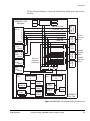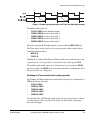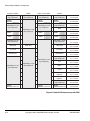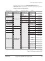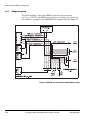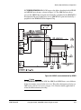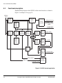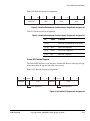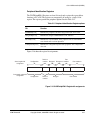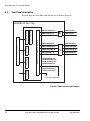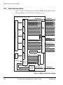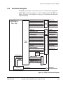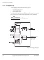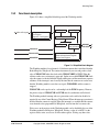
1
ARM926EJ-S Development Chip
Reference Manual
Copyright © 2004, 2006 ARM Limited. All rights reserved.
ARM DDI 0287B
ARM926EJ-S Development Chip
Reference Manual
Copyright © 2004, 2006 ARM Limited. All rights reserved.
Release Information
Change history
Description
Issue
Change
April 2004
A
New document
August 2006
B
Second release, updated to fix defects on AHB monitor and AHB bus
graphics.
Proprietary Notice
Words and logos marked with® or ™ are registered trademarks or trademarks of ARM Limited in the EU and
other countries, except as otherwise stated below in this proprietary notice. Other brands and names
mentioned herein may be the trademarks of their respective owners.
Neither the whole nor any part of the information contained in, or the product described in, this document
may be adapted or reproduced in any material form except with the prior written permission of the copyright
holder.
The product described in this document is subject to continuous developments and improvements. All
particulars of the product and its use contained in this document are given by ARM Limited in good faith.
However, all warranties implied or expressed, including but not limited to implied warranties of
merchantability, or fitness for purpose, are excluded.
This document is intended only to assist the reader in the use of the product. ARM Limited shall not be liable
for any loss or damage arising from the use of any information in this document, or any error or omission in
such information, or any incorrect use of the product.
Confidentiality Status
This document is Non-Confidential. The right to use, copy and disclose this document may be subject to
license restrictions in accordance with the terms of the agreement entered into by ARM and the party that
ARM delivered this document to.
Product Status
The information in this document is final, that is for a developed product.
Web Address
http://www.arm.com
ii
Copyright © 2004, 2006 ARM Limited. All rights reserved.
ARM DDI 0287B
Conformance Notices
This section contains conformance notices.
Federal Communications Commission Notice
This device is test equipment and consequently is exempt from part 15 of the FCC Rules under section 15.103
(c).
CE Declaration of Conformity
A system using this development chip should be powered down when not in use.
The ARM926PXP development chip generates, uses, and can radiate radio frequency energy and may cause
harmful interference to radio communications. However, there is no guarantee that interference will not occur
in a particular installation. If equipment using the ARM926PXP development chip causes harmful
interference to radio or television reception, which can be determined by turning the equipment off or on, you
are encouraged to try to correct the interference by one or more of the following measures:
•
ensure attached cables do not lie across the card
•
reorient the receiving antenna
•
increase the distance between the equipment and the receiver
•
connect the equipment into an outlet on a circuit different from that to which the receiver is connected
•
consult the dealer or an experienced radio/TV technician for help
Note
It is recommended that wherever possible shielded interface cables be used.
ARM DDI 0287B
Copyright © 2004, 2006 ARM Limited. All rights reserved.
iii
iv
Copyright © 2004, 2006 ARM Limited. All rights reserved.
ARM DDI 0287B
Contents
ARM926EJ-S Development Chip Reference
Manual
Preface
About this document .................................................................................. xviii
Feedback ................................................................................................... xxiii
Part A
Chapter 1
Introduction and Configuration
Introduction
1.1
1.2
1.3
Chapter 2
System Controller and Configuration Logic
2.1
2.2
2.3
2.4
2.5
2.6
ARM DDI 0287B
About the ARM926EJ-S Development Chip ............................................... 1-2
Functional description ................................................................................. 1-4
External interfaces ...................................................................................... 1-9
About the System Controller ....................................................................... 2-2
Clock control ............................................................................................. 2-13
External configuration signals ................................................................... 2-19
JTAG logic ................................................................................................ 2-25
Implementation details for the ARM926EJ-S and system controller ......... 2-28
Control, configuration, and test signals on pads ....................................... 2-30
Copyright © 2004, 2006 ARM Limited. All rights reserved.
v
Contents
Chapter 3
Memory Map and Memory Configuration
3.1
3.2
3.3
Part B
Chapter 4
Controllers and Peripherals
AHB Monitor
4.1
4.2
4.3
4.4
Chapter 5
About the ARM PrimeCell MPMC (GX175) .............................................. 10-2
Functional description ............................................................................... 10-6
MPMC signals on pads ............................................................................. 10-8
Real-Time Clock (RTC)
11.1
11.2
vi
About the ARM PrimeCell GPIO (PL061) ................................................... 9-2
Functional description ................................................................................. 9-3
GPIO signals on pads ................................................................................. 9-5
Multi-Port Memory Controller (MPMC)
10.1
10.2
10.3
Chapter 11
About the Direct Memory Access Controller (PL080) ................................. 8-2
Functional description ................................................................................. 8-4
DMA signals on pads .................................................................................. 8-7
General Purpose Input Output (GPIO)
9.1
9.2
9.3
Chapter 10
About the ARM MBX HR-S ......................................................................... 7-2
Memory map and registers ......................................................................... 7-6
Direct Memory Access Controller (DMAC)
8.1
8.2
8.3
Chapter 9
About the MOVE Coprocessor ................................................................... 6-2
MBX HR-S Graphics Accelerator
7.1
7.2
Chapter 8
About the CLCDC ....................................................................................... 5-2
Functional description ................................................................................. 5-4
Hardware cursor extension to PL110 ......................................................... 5-7
CLCD signals on pads .............................................................................. 5-31
MOVE Coprocessor
6.1
Chapter 7
About the AHB monitor ............................................................................... 4-2
Functional description ................................................................................. 4-3
AHB Monitor registers .............................................................................. 4-23
AHB Monitor signals on pads ................................................................... 4-42
Color LCD Controller (CLCDC)
5.1
5.2
5.3
5.4
Chapter 6
Overview of the AMBA buses in the ARM926EJ-S Development Chip ...... 3-2
Memory map options ................................................................................ 3-15
AHB signals to pads ................................................................................. 3-32
About the Real Time Clock ....................................................................... 11-2
Functional description ............................................................................... 11-3
Copyright © 2004, 2006 ARM Limited. All rights reserved.
ARM DDI 0287B
Contents
Chapter 12
Smart Card Interface (SCI)
12.1
12.2
12.3
Chapter 13
Synchronous Static Memory Controller (SSMC)
13.1
13.2
13.3
Chapter 14
About the Watchdog module (SP805) ...................................................... 19-2
Functional description ............................................................................... 19-3
Pad signals by function ............................................................................... A-2
Mechanical and Electrical Specifications
B.1
B.2
ARM DDI 0287B
18-2
18-3
18-4
18-6
Signals on Pads
A.1
Appendix B
About the VFP9-S coprocessor ................................................................
ARMv5TE coprocessor extensions ...........................................................
VFP9-S system control and status registers .............................................
Modes of operation ...................................................................................
Watchdog Timer
19.1
19.2
Appendix A
About the ARM PrimeCell Vectored Interrupt Controller (PL190) ............. 17-2
Functional description ............................................................................... 17-4
VIC signals on pads ................................................................................ 17-11
ARM Vector Floating Point Coprocessor (VFP9)
18.1
18.2
18.3
18.4
Chapter 19
About the ARM PrimeCell UART (PL011) ................................................. 16-2
Functional description ............................................................................... 16-4
UART signals on pads .............................................................................. 16-8
Vectored Interrupt Controller (VIC)
17.1
17.2
17.3
Chapter 18
About the ARM Dual-Timer module (SP804) ............................................ 15-2
Functional description ............................................................................... 15-3
UART Controller
16.1
16.2
16.3
Chapter 17
About the ARM PrimeCell SSP (PL022) ................................................... 14-2
Functional description ............................................................................... 14-4
SSP signals on pads ................................................................................. 14-6
Dual Timer/Counters
15.1
15.2
Chapter 16
About the ARM PrimeCell SSMC (PL093) ................................................ 13-2
Functional description ............................................................................... 13-5
SSMC signals on pads .............................................................................. 13-9
Synchronous Serial Port (SSP)
14.1
14.2
14.3
Chapter 15
About the ARM SCI ................................................................................... 12-2
Functional description ............................................................................... 12-4
SCI signals on pads .................................................................................. 12-6
Mechanical details ...................................................................................... B-2
Electrical specification ................................................................................. B-3
Copyright © 2004, 2006 ARM Limited. All rights reserved.
vii
Contents
Appendix C
Timing Specification
C.1
C.2
C.3
C.4
viii
About the timing parameters ......................................................................
AHB bus timing ...........................................................................................
Memory timing ............................................................................................
Peripheral timing .........................................................................................
Copyright © 2004, 2006 ARM Limited. All rights reserved.
C-2
C-3
C-4
C-5
ARM DDI 0287B
List of Tables
ARM926EJ-S Development Chip Reference
Manual
Table 1-1
Table 2-1
Table 2-1
Table 2-2
Table 2-3
Table 2-4
Table 2-5
Table 2-6
Table 2-7
Table 2-8
Table 3-1
Table 3-1
Table 3-2
Table 3-1
Table 3-2
Table 3-3
Table 4-1
Table 4-2
Table 4-3
Table 4-4
ARM DDI 0287B
Change history .............................................................................................................. ii
MPMC port allocation .............................................................................................. 1-10
System mode control signal states ........................................................................... 2-9
External peripheral clocks and clock control signals ............................................... 2-18
Configuration signal sources ................................................................................... 2-19
Configuration signal destinations ............................................................................ 2-20
ARM926EJ-S signals .............................................................................................. 2-30
ETM signals ............................................................................................................ 2-30
Reset and configuration signals .............................................................................. 2-31
Clock signals ........................................................................................................... 2-32
JTAG TAP signals ................................................................................................... 2-33
On-chip bridge selection ......................................................................................... 3-10
DMA APB peripheral base addresses ..................................................................... 3-30
Core APB peripheral base addresses ..................................................................... 3-30
AHB M1 signals ....................................................................................................... 3-32
AHB M2 signals ....................................................................................................... 3-33
AHB S signals ......................................................................................................... 3-34
Cycle states ............................................................................................................... 4-4
Sample output ........................................................................................................... 4-5
Bus state bit patterns ................................................................................................ 4-6
Bit patterns for GXI states for read channel .............................................................. 4-9
Copyright © 2004, 2006 ARM Limited. All rights reserved.
ix
List of Tables
Table 4-5
Table 4-6
Table 4-7
Table 4-8
Table 4-9
Table 4-10
Table 4-11
Table 4-12
Table 4-13
Table 4-14
Table 4-1
Table 4-1
Table 4-2
Table 4-1
Table 4-1
Table 5-1
Table 5-2
Table 5-3
Table 5-4
Table 5-5
Table 5-6
Table 5-7
Table 5-8
Table 5-9
Table 5-10
Table 5-1
Table 5-2
Table 5-3
Table 5-4
Table 5-5
Table 5-6
Table 5-7
Table 5-8
Table 5-9
Table 5-10
Table 5-11
Table 5-12
Table 5-13
Table 5-14
Table 5-15
Table 5-16
Table 5-17
Table 5-18
Table 5-19
Table 5-20
Table 7-1
Table 8-1
x
Bit patterns for GXI state for address channel ........................................................ 4-10
Event counters for the ARM-I layer ......................................................................... 4-13
CLCDC events ........................................................................................................ 4-14
DMA 0 events ......................................................................................................... 4-15
DMA 1 events ......................................................................................................... 4-16
EXP layer events .................................................................................................... 4-17
D layer events ......................................................................................................... 4-19
GXI events .............................................................................................................. 4-21
Other events ........................................................................................................... 4-22
AHB Monitor registers ............................................................................................. 4-24
<layer>WaitThreshold ............................................................................................. 4-36
GxiPageSize ........................................................................................................... 4-38
AHBMONCtrlReg .................................................................................................... 4-39
AHBMONPeriphID .................................................................................................. 4-40
Output pad signal descriptions ............................................................................... 4-42
PrimeCell CLCDC register differences ..................................................................... 5-6
Supported cursor images .......................................................................................... 5-8
32x32 cursor base addresses ................................................................................. 5-12
LBBP buffer to pixel mapping 32x32 Cursor0 for datawords [31:16] ...................... 5-12
LBBP buffer to pixel mapping 32x32 Cursor0 for datawords [15:0] ........................ 5-13
LBBP buffer to pixel mapping 64x64 for datawords [31:16] .................................... 5-13
LBBP buffer to pixel mapping 64x64 for datawords [15:0] ...................................... 5-14
32x32 software mask storage ................................................................................. 5-15
64x64 software mask storage ................................................................................. 5-15
Pixel encoding ........................................................................................................ 5-16
PrimeCell CLCDC register summary ...................................................................... 5-17
ClcdCrsrCtrl Register bit assignments .................................................................... 5-19
ClcdCrsrConfig Register bit assignments ............................................................... 5-20
ClcdCrsrPalette0 and ClcdCrsrPalette1 Register bit assignments ......................... 5-21
ClcdCrsrXY Register bit assignments ..................................................................... 5-22
ClcdCrsrClip Register bit assignments ................................................................... 5-23
ClcdCrsrIMSC Register bit assignments ................................................................ 5-24
ClcdCrsrICR Register bit assignments ................................................................... 5-24
ClcdCrsrRIS Register bit assignments ................................................................... 5-25
ClcdCrsrMIS Register bit assignments ................................................................... 5-26
Peripheral Identification Register options ............................................................... 5-27
CLCDPeriphID0 Register bit assignments .............................................................. 5-28
CLCDPeriphID1 Register bit assignments .............................................................. 5-28
CLCDPeriphID2 Register bit assignments .............................................................. 5-28
CLCDPeriphID3 Register bit assignments .............................................................. 5-28
CLCDPCellID0 Register bit assignments ............................................................... 5-29
CLCDPCellID1 Register bit assignments ............................................................... 5-29
CLCDPCellID2 Register bit assignments ............................................................... 5-30
CLCDPCellID3 Register bit assignments ............................................................... 5-30
External pad output signals .................................................................................... 5-31
MBX HR-S memory map .......................................................................................... 7-6
DMA channel allocation ............................................................................................ 8-5
Copyright © 2004, 2006 ARM Limited. All rights reserved.
ARM DDI 0287B
List of Tables
Table 8-1
Table 9-1
Table 9-2
Table 10-1
Table 12-1
Table 12-2
Table 13-1
Table 13-2
Table 14-1
Table 16-1
Table 17-1
Table 17-2
Table 18-1
Table A-1
Table B-1
Table B-2
Table B-3
Table C-1
Table C-2
Table C-3
ARM DDI 0287B
DMA request and response signal descriptions ........................................................ 8-7
On-chip signal descriptions ....................................................................................... 9-4
Pad signal descriptions ............................................................................................. 9-5
Pad interface and control signal descriptions .......................................................... 10-8
Interrupts ................................................................................................................. 12-5
SCI signals .............................................................................................................. 12-6
Internal signal descriptions ...................................................................................... 13-8
Pad signals .............................................................................................................. 13-9
Pad signal descriptions ........................................................................................... 14-6
Pad signal descriptions ........................................................................................... 16-8
Tied off or unused signals ..................................................................................... 17-10
Interrupt controller pad signals .............................................................................. 17-11
Access to control registers ...................................................................................... 18-5
Pad signals ................................................................................................................ A-2
Interface signal electrical characteristics ................................................................... B-3
Operating ranges ...................................................................................................... B-3
Power estimate ......................................................................................................... B-4
ARM926EJ-S Development Chip bus timing ........................................................... C-3
ARM926EJ-S Development Chip memory timing .................................................... C-4
Peripherals and controller timing .............................................................................. C-5
Copyright © 2004, 2006 ARM Limited. All rights reserved.
xi
List of Tables
xii
Copyright © 2004, 2006 ARM Limited. All rights reserved.
ARM DDI 0287B
List of Figures
ARM926EJ-S Development Chip Reference
Manual
Figure 1-1
Figure 1-2
Figure 1-3
Figure 2-1
Figure 2-2
Figure 2-3
Figure 2-4
Figure 2-5
Figure 2-6
Figure 2-7
Figure 2-8
Figure 3-1
Figure 3-2
Figure 3-3
Figure 3-4
Figure 3-5
Figure 3-6
Figure 3-7
Figure 3-8
Figure 3-9
Figure 3-10
ARM DDI 0287B
Typical application ..................................................................................................... 1-2
ARM926EJ-S Development Chip block diagram ....................................................... 1-3
Default system bus memory map for ARM DATA AHB bus .................................... 1-12
Enable signal generation for the Timer and Watchdog modules .............................. 2-5
Reference frequency select for Watchdog and Timer modules clock enable ........... 2-6
System mode control state machine ......................................................................... 2-8
Clock and reset block diagram ................................................................................ 2-13
External clock signals and clock selection .............................................................. 2-14
Power-on configuration block diagram .................................................................... 2-24
JTAG Test Access Port ........................................................................................... 2-26
Multi-ICE synchronization ....................................................................................... 2-27
Bus matrix configuration ............................................................................................ 3-4
AHB M1 interface ...................................................................................................... 3-7
AHB M2 interface ...................................................................................................... 3-8
AHB S interface ....................................................................................................... 3-13
Memory control signals ........................................................................................... 3-16
Default AHB memory map with SMC ...................................................................... 3-18
AHB memory map without SMC ............................................................................. 3-19
AHB M1 access determined by address range ....................................................... 3-20
AHB M1 access determined by ARM D .................................................................. 3-21
Default AHB memory map with no bridge remap and SMC .................................... 3-22
Copyright © 2004, 2006 ARM Limited. All rights reserved.
xiii
List of Figures
Figure 3-11
Figure 3-12
Figure 3-13
Figure 3-14
Figure 3-15
Figure 3-16
Figure 3-17
Figure 3-18
Figure 3-19
Figure 3-20
Figure 4-1
Figure 4-2
Figure 4-3
Figure 4-4
Figure 5-1
Figure 5-2
Figure 5-3
Figure 5-4
Figure 5-5
Figure 5-6
Figure 5-7
Figure 5-8
Figure 5-9
Figure 5-10
Figure 5-11
Figure 5-12
Figure 5-13
Figure 5-14
Figure 5-15
Figure 5-16
Figure 5-17
Figure 6-1
Figure 7-1
Figure 7-2
Figure 8-1
Figure 9-1
Figure 10-1
Figure 11-1
Figure 12-1
Figure 13-1
Figure 13-2
Figure 13-3
Figure 14-1
Figure 15-1
Figure 16-1
Figure 17-1
Figure 17-2
xiv
AHB memory map with bridge remap and SMC ..................................................... 3-23
AHB memory map with bridge remap and no SMC ................................................ 3-24
Supported address remap functionality for ARM D AHB ........................................ 3-25
Alias for REMAPSTATIC LOW ............................................................................... 3-26
Alias for REMAPSTATIC HIGH and MPMCnSMC LOW ........................................ 3-27
Alias for REMAPSTATIC HIGH and MPMCnSMC HIGH ....................................... 3-27
Alias for REMAPEXTERNAL HIGH and CFGBRIDGEMEMMAP HIGH ................ 3-28
Alias for REMAPEXTERNAL HIGH and CFGBRIDGEMEMMAP LOW ................. 3-28
APB map ................................................................................................................. 3-29
MBX map ................................................................................................................ 3-31
AHB monitor block diagram ...................................................................................... 4-3
AHB Monitor packet format ....................................................................................... 4-4
Peripheral ID register .............................................................................................. 4-40
PrimeCell ID register ............................................................................................... 4-41
CLCDC internal organization .................................................................................... 5-4
CLCDC block diagram .............................................................................................. 5-5
Hardware cursor block diagram ................................................................................ 5-7
Hardware cursor movement ..................................................................................... 5-9
Hardware cursor clipping ........................................................................................ 5-10
Hardware cursor image format ............................................................................... 5-11
ClcdCrsrCtrl Register bit assignments .................................................................... 5-18
ClcdCrsrConfig Register bit assignments ............................................................... 5-20
ClcdCrsrPalette0 and ClcdCrsrPalette1 Register bit assignments ......................... 5-21
ClcdCrsrXY Register bit assignments ..................................................................... 5-21
ClcdCrsrClip Register bit assignments ................................................................... 5-22
ClcdCrsrIMSC Register bit assignments ................................................................ 5-23
ClcdCrsrICR Register bit assignments ................................................................... 5-24
ClcdCrsrRIS Register bit assignments ................................................................... 5-25
ClcdCrsrMIS Register bit assignments ................................................................... 5-26
CLCDPeriphID0-3 Register bit assignments .......................................................... 5-27
CLCDCPCellID0-3 Register bit assignments .......................................................... 5-29
MOVE overview ........................................................................................................ 6-3
ARM MBX HR-S top level block diagram ................................................................. 7-2
MMU address translation .......................................................................................... 7-8
DMAC interface block diagram ................................................................................. 8-4
GPIO output control .................................................................................................. 9-3
MPMC PrimeCell block diagram ............................................................................. 10-6
PrimeCell RTC ........................................................................................................ 11-3
SCI block diagram .................................................................................................. 12-4
SSMC interface block diagram ............................................................................... 13-5
Address and control multiplexor ............................................................................. 13-6
Data multiplexor ...................................................................................................... 13-7
PrimeCell SSP block diagram ................................................................................. 14-3
Simplified block diagram ......................................................................................... 15-4
PrimeCell UART block diagram .............................................................................. 16-4
VIC block diagram .................................................................................................. 17-4
Interrupt request logic ............................................................................................. 17-5
Copyright © 2004, 2006 ARM Limited. All rights reserved.
ARM DDI 0287B
List of Figures
Figure 17-3
Figure 17-4
Figure 17-5
Figure 17-6
Figure 19-1
Figure B-1
Figure C-1
ARM DDI 0287B
Nonvectored FIQ interrupt logic .............................................................................. 17-6
Nonvectored IRQ interrupt logic .............................................................................. 17-6
Vectored interrupt block .......................................................................................... 17-7
Interrupt priority logic ............................................................................................... 17-8
Simplified block diagram ......................................................................................... 19-3
BGA numbering, ball side view ................................................................................. B-2
AC timing example ................................................................................................... C-2
Copyright © 2004, 2006 ARM Limited. All rights reserved.
xv
List of Figures
xvi
Copyright © 2004, 2006 ARM Limited. All rights reserved.
ARM DDI 0287B
Preface
This preface introduces the ARM926EJ-S Development Chip Reference Manual. It
contains the following sections:
•
About this document on page xviii
•
Feedback on page xxiii.
ARM DDI 0287B
Copyright © 2004, 2006 ARM Limited. All rights reserved.
xvii
Preface
About this document
This document provides an overview of the ARM926EJ-S Development Chip and a
description of the modules in it. For details on the registers and programmer’s interface,
see the Technical Reference Manual for the individual controller.
Intended audience
This document has been written for experienced hardware and software developers
using the ARM926EJ-S Development Chip as part of an existing development system.
Organization
This document is organized into the following chapters:
Chapter 1 Introduction
Read this chapter for an introduction to the ARM926EJ-S Development
Chip.
Chapter 2 System Controller and Configuration Logic
Read this chapter for a description of the clock and configuration logic
that is associated with the system controller.
Chapter 3 Memory Map and Memory Configuration
Read this chapter for a description of the AHB buses and the memory
map for the ARM926EJ-S Development Chip.
Chapter 4 AHB Monitor
Read this chapter for a description of the bus monitor.
Chapter 5 Color LCD Controller (CLCDC)
Read this chapter for a description of the display controller.
Chapter 6 MOVE Coprocessor
Read this chapter for a description of the MOVE graphic coprocessor.
Chapter 7 MBX HR-S Graphics Accelerator
Read this chapter for a description of the MBX graphic coprocessor.
Chapter 8 Direct Memory Access Controller (DMAC)
Read this chapter for a description of the DMA controller.
xviii
Copyright © 2004, 2006 ARM Limited. All rights reserved.
ARM DDI 0287B
Preface
Chapter 9 General Purpose Input Output (GPIO)
Read this chapter for a description of the GPIO.
Chapter 10 Multi-Port Memory Controller (MPMC)
Read this chapter for a description of the MPMC.
Chapter 11 Real-Time Clock (RTC)
Read this chapter for a description of the RTC controller.
Chapter 12 Smart Card Interface (SCI)
Read this chapter for a description of the SCI.
Chapter 13 Synchronous Static Memory Controller (SSMC)
Read this chapter for a description of the SSMC.
Chapter 14 Synchronous Serial Port (SSP)
Read this chapter for a description of the SSP.
Chapter 15 Dual Timer/Counters
Read this chapter for a description of the dual timer/counter.
Chapter 17 Vectored Interrupt Controller (VIC)
Read this chapter for a description of the VIC controller.
Chapter 18 ARM Vector Floating Point Coprocessor (VFP9)
Read this chapter for a description of the VFP9.
Chapter 19 Watchdog Timer
Read this chapter for a description of the watchdog controller.
Appendix A Signals on Pads
Refer to this appendix for a list of signals on the input/output pads of the
ARM926EJ-S Development Chip.
Appendix B Mechanical and Electrical Specifications
Read this appendix for details on the ARM926EJ-S Development Chip
mechanical packaging and the electrical specifications.
Appendix C Timing Specification
Refer to this appendix for timing specifications.
ARM DDI 0287B
Copyright © 2004, 2006 ARM Limited. All rights reserved.
xix
Preface
Typographical conventions
The following typographical conventions are used in this document:
bold
Highlights ARM signal names within text, and interface elements
such as menu names. This style is also used for emphasis in
descriptive lists where appropriate.
italic
Highlights special terminology, cross-references and citations.
monospace
Denotes text that can be entered at the keyboard, such as
commands, file names and program names, and source code.
monospace
Denotes a permitted abbreviation for a command or option. The
underlined text can be entered instead of the full command or
option name.
monospace italic
Denotes arguments to commands or functions where the argument
is to be replaced by a specific value.
monospace bold
Denotes language keywords when used outside example code.
Further reading
This section lists related publications by ARM Limited and other companies that might
provide additional information.
ARM publications
The following publication provides information about the registers and interfaces on the
ARM926EJ-S Development Chip:
•
ARM926EJ-S Technical Reference Manual (ARM DDI 0198)
•
ARM926EJ-S™ PrimeXsys Wireless Platform Virtual Component Technical
Reference Manual (ARM DDI 0232)
•
ARM926EJ-S™ PrimeXsys Platform Virtual Component User Guide (ARM DUI
0213)
•
ARM MOVE Coprocessor Technical Reference Manual (ARM DDI 0251)
•
ARM VFP9-S Coprocessor Technical Reference Manual (ARM DDI 0238)
•
ARM MBX HR-S Graphics Core Technical Reference Manual (ARM DDI 0241).
xx
Copyright © 2004, 2006 ARM Limited. All rights reserved.
ARM DDI 0287B
Preface
The following publications provide reference information about the ARM architecture:
•
AMBA™ Specification (ARM IHI 0011)
•
ARM Architecture Reference Manual (ARM DDI 0100).
The following publications provides information about related ARM products and
toolkits:
•
Multi-ICE™ User Guide (ARM DUI 0048)
•
RealView™ ICE User Guide (ARM DUI 0155)
•
Trace Debug Tools User Guide (ARM DUI 0118)
•
ARM MultiTrace® User Guide (ARM DUI 0150)
•
ARM LT-XC2V4000+ Versatile Logic Tile User Guide (ARM DUI 0186)
•
RealView™ Debugger User Guide (ARM DUI 0153)
•
RealView Compilation Tools Compilers and Libraries Guide (ARM DUI 0205)
•
RealView Compilation Tools Developer Guide (ARM DUI 0203)
•
RealView Compilation Tools Linker and Utilities Guide (ARM DUI 0206).
The following publications provide information about ARM PrimeCell® and other
processor devices:
•
ARM PrimeCell Color LCD Controller (PL110) Technical Reference Manual
(ARM DDI 0161)
•
ARM PrimeCell DMA (PL080) Technical Reference Manual (ARM DDI 0196)
•
ARM Dual-Timer Module (SP804) Technical Reference Manual (ARM DDI
0271)
•
ARM PrimeCell GPIO (PL061) Technical Reference Manual (ARM DDI 0190)
•
ARM Multiport Memory Controller (GX175) Technical Reference Manual (ARM
DDI 0277)
•
ARM PrimeCell Real Time Clock Controller (PL031) Technical Reference
Manual (ARM DDI 0224)
•
ARM PrimeCell Smart Card Interface (PL131) Technical Reference Manual
(ARM DDI 0228)
•
ARM PrimeCell Synchronous Serial Port Controller (PL022) Technical Reference
Manual (ARM DDI 0194)
•
ARM PrimeCell Static Memory Controller (PL093) Technical Reference Manual
(ARM DDI 236)
•
ARM PrimeCell System Controller (SP810) Technical Reference Manual (ARM
DDI 0254)
•
ARM PrimeCell UART (PL011) Technical Reference Manual (ARM DDI 0183)
•
ARM PrimeCell Vector Interrupt Controller (PL190) Technical Reference
Manual (ARM DDI 0181)
ARM DDI 0287B
Copyright © 2004, 2006 ARM Limited. All rights reserved.
xxi
Preface
•
•
ARM PrimeCell Watchdog Controller (SP805) Technical Reference Manual
(ARM DDI 0270)
ETM9 Technical Reference Manual (ARM DDI 0157)
Other publications
The following publication describes the JTAG ports with which Multi-ICE
communicates:
•
xxii
IEEE Standard Test Access Port and Boundary Scan Architecture (IEEE Std.
1149.1).
Copyright © 2004, 2006 ARM Limited. All rights reserved.
ARM DDI 0287B
Preface
Feedback
ARM Limited welcomes feedback both on the ARM926EJ-S Development Chip and on
the documentation.
Feedback on this document
If you have any comments about this document, send email to [email protected] giving:
•
the document title
•
the document number
•
the page number(s) to which your comments refer
•
an explanation of your comments.
General suggestions for additions and improvements are also welcome.
Feedback on the ARM926EJ-S Development Chip
If you have any comments or suggestions about these products, contact your supplier
giving:
•
the product name
•
an explanation of your comments.
ARM DDI 0287B
Copyright © 2004, 2006 ARM Limited. All rights reserved.
xxiii
Preface
xxiv
Copyright © 2004, 2006 ARM Limited. All rights reserved.
ARM DDI 0287B
Part A
Introduction and Configuration
Chapter 1
Introduction
This chapter introduces the ARM926EJ-S Development Chip. It contains the following
sections:
•
About the ARM926EJ-S Development Chip on page 1-2
•
Functional description on page 1-4
•
External interfaces on page 1-9.
ARM DDI 0287B
Copyright © 2004, 2006 ARM Limited. All rights reserved.
1-1
Introduction
1.1
About the ARM926EJ-S Development Chip
The ARM926EJ-S Development Chip is used in ARM development boards and enables
you to develop software for products based on the ARM926EJ-S PrimeXSys Wireless
Platform.
A typical application of the ARM926EJ-S Development Chip is shown in Figure 1-1.
Debug and test connectors
Trace port
JTAG
Monitor
VFP9
JTAG
MOVE
AHB
monitor
CLCDC
(PL110)
MPMC
(GX175)
Multi-layer AHB
and bus switch
MBX
HR-S
Expansion
bus
MM
card
Ethernet
LAN chip
USB
chip
ARM926EJ-S
Dev. Chip
ETM9
ARM926EJ-S CPU
SDRAM
Color
LCD
display
MMCI
(PL131)
AHB
ports
M1, M2,
and S
Ethernet and
USB interface
FPGA
bus interface and
controller
Flash
ROM
SSMC
(PL093)
APB
bridge
SRAM
4x
GPIO
(PL061)
WATCHDOG
(SP805)
2 x Dual
timer
(SP804)
System Controller
Clock and reset
controller
PLL
32 GPIO lines
Xtal osc
DMA APB
RTC
(PL031)
Core APB
1Hz
clock
APB
bridge
External
Control
AACI
DMA
registers (PL041)
and
interrupt
VIC
(PL190)
DMAC
(PL080)
SSP
(PL022)
SSP
interface
SCI
(PL131)
SIM card
Programmable
oscillators for
on-chip interfaces
3 x UART (SP802)
IRDA
Keyboard
interface
Audio
CODEC
RS232
Figure 1-1 Typical application
1-2
Copyright © 2004, 2006 ARM Limited. All rights reserved.
ARM DDI 0287B
Introduction
The block diagram in Figure 1-2 shows the internal buses and the master and slave bus
interfaces.
ETM9
ARM926EJ-S
ARM Data AHB
ARM Instruction AHB
CLCDC AHB
DMA1 AHB
EXP AHB
DMA0 AHB
M
CLCDC
(PL110)
config S
M
M
config S
DMAC
(PL080)
VIC
(PL190)
config S
M
S
M
Bus
interface
S
S
S
S
S
S
config S
S
AHB
Mon.
MBX interface port
MPMC
(GX175)
S
Bus matrix
multiplexors
and decoders
MBX HR-S
accelerator
JTAG
M M
VFP9
S
Bus
interface
MOVE
Bus
interface
ARM926EJ-S PXP
Subsystem
S
AHB S
expansion
bus
M
AHB M2
expansion
bus
M
AHB M1
expansion
bus
SSMC
S
(PL093)
config S
Core
APB
Dual Timer
(SP804) x2
GPIO x4
(PL061)
DMA
APB
S
AHB/APB bridge
M
RTC
(PL031)
Watchdog
(SP805
System
Controller
(SP810)
S
AHB/APB bridge
M
SSP1
(PL022)
UART x3
(PL011)
SCI
(PL131)
ARM926EJ-S
Dev. Chip
Figure 1-2 ARM926EJ-S Development Chip block diagram
ARM DDI 0287B
Copyright © 2004, 2006 ARM Limited. All rights reserved.
1-3
Introduction
1.2
Functional description
The ARM926EJ-S Development Chip comprises the following functional blocks:
ARM926EJ-S
This is a cached ARM CPU including Instruction and Data caches,
Memory Management Unit (MMU), and Tightly Coupled Memory
(TCM). It supports the JazelleTM extensions for Java acceleration.
The ARM926EJ-S processor used with the ARM926EJ-S Development
Chip is configured with 32KB instruction and data caches and 32KB
TCMs.
The release version used is ARM926EJ-S r0p3-00rel0. The PrimeXsys
Wireless Platform version is r2p0.
For more information on the ARM926EJ-S, see the ARM926EJ-S
Technical Reference Manual.
MOVE coprocessor
The MOVE coprocessor is a video encoding acceleration coprocessor
designed to accelerate Motion Estimation (ME) algorithms within
block-based video encoding schemes such as MPEG4 and H.263. This is
done by providing support for the execution of Sum of Absolute
Differences (SAD) calculations, which account for most of the
processing activity within an ME algorithm. These algorithms require
many comparisons between 8x8 pixel blocks to made between a current
frame and a reference frame.
The release version used is MOVE r3p0-00bet0.
For more information on the MOVE coprocessor, see the ARM MOVE
Coprocessor Technical Reference Manual and Chapter 6 MOVE
Coprocessor.
VFP9 coprocessor
The VFP9-S coprocessor is an implementation of the Vector
Floating-Point architecture version 2 (VFPv2) and provides
floating-point computation that is fully compliant with the ANSI/IEEE
Std 754-1985, IEEE Standard for Binary Floating-Point Arithmetic. The
VFP9-S coprocessor supports all addressing modes described in section
C5 of the ARM Architecture Reference Manual.
The release version used is VFP9-S r1p1.
For more information on the VFP9 coprocessor, see the ARM VFP9-S
Coprocessor Technical Reference Manual and Chapter 18 ARM Vector
Floating Point Coprocessor (VFP9).
1-4
Copyright © 2004, 2006 ARM Limited. All rights reserved.
ARM DDI 0287B
Introduction
AHB Monitor
The AHB Monitor block outputs transaction information for the buses in
the ARM926EJ-S Development Chip and is used to evaluate performance
and bandwidth utilization analysis.
For more information on the AHB monitor, see Chapter 4 AHB Monitor.
MBX Graphics Accelerator
The ARM MBX HR-S is a graphics accelerator that operates on 3D scene
data. Triangles are written directly to the Tile Accelerator on a First In
First Out (FIFO) basis so that the CPU is not stalled.
The release version used is MBX HR-S r1p2.
For more information on the MBX accelerator, see the ARM MBX HR-S
Graphics Core Technical Reference Manual and Chapter 7 MBX HR-S
Graphics Accelerator.
System Controller
This provides a control interface for clock generation components
external to the chip. It also controls system-wide and peripherals-specific
energy management features.
The release version used is SP810 SYSCTRL r0p0-00ltd0.
For more information on the system controller, see the ARM PrimeCell
System Controller (SP810) Technical Reference Manual and Chapter 2
System Controller and Configuration Logic.
Multi-Port Memory Controller (MPMC)
The MPMC can be used to interface with Synchronous Dynamic Random
Access Memory (SDRAM) and static memory devices.
The release version used is GX175 MPMC r0p0-00alp2.
For more information on the MPMC, see the ARM Multiport Memory
Controller (GX175) Technical Reference Manual and Chapter 10
Multi-Port Memory Controller (MPMC).
Synchronous Static Memory Controller (SSMC)
The SSMC interfaces to off-chip static memory devices such as Read
Only Memory (ROM), Static Random Access Memory (SRAM), or static
flash memory.
The release version used is PL093 SSMC r0p0-00ltd0.
For more information on the SSMC, see the ARM PrimeCell Static
Memory Controller (PL093) Technical Reference Manual and Chapter 13
Synchronous Static Memory Controller (SSMC).
ARM DDI 0287B
Copyright © 2004, 2006 ARM Limited. All rights reserved.
1-5
Introduction
Direct Memory Access Controller (DMAC)
Direct memory access can be used with DMA peripherals. FIFO fill and
empty requests from these peripherals can be serviced immediately by
the DMAC without CPU interaction. Memory-to-memory DMA is also
supported.
The release version used is PL080 DMAC REL1v1.
For more information on DMA, see the ARM PrimeCell DMA (PL080)
Technical Reference Manual and Chapter 8 Direct Memory Access
Controller (DMAC).
Vectored Interrupt Controller (VIC)
The VIC enables the interrupt handler software to quickly dispatch
interrupt service routines in response to peripheral interrupts.
The release version used is PL190 VIC 1v1.
For more information on the VIC, see the ARM PrimeCell Vector
Interrupt Controller (PL190) Technical Reference Manual and
Chapter 17 Vectored Interrupt Controller (VIC).
Embedded Trace Macrocell (ETM9)
The ETM9 provides a trace port for real-time debug.
The release version used is ETM9 Rev2a. The ETM configuration for the
ARM926EJ-S Development Chip is Medium-Plus.
For more information on the ETM9, see the ETM9 Technical Reference
Manual.
Real Time Clock (RTC)
The RTC provides a one-second resolution clock. This keeps time when
the ARM926EJ-S Development Chip is inactive and can be used to wake
the chip up when a programmed alarm time is reached.
The release version used is PL031 RTC 1v0.
For more information on the RTC, see the ARM PrimeCell Real Time
Clock Controller (PL031) Technical Reference Manual and Chapter 11
Real-Time Clock (RTC).
Timer modules
The ARM926EJ-S Development Chip provides two Timer modules.
They can be used to, for example, generate periodic and timed interrupts
required by operating system services.
The release version used is SP804 TIMER r1p0-02ltd0.
1-6
Copyright © 2004, 2006 ARM Limited. All rights reserved.
ARM DDI 0287B
Introduction
For more information on the timers, see the ARM Dual-Timer Module
(SP804) Technical Reference Manual and Chapter 15 Dual
Timer/Counters.
Watchdog module
This is used to trigger a system reset in the event of software failure.
The release version used is SP805 WDOG r1p0-02ltd0.
For more information on the Watchdog monitor, see the ARM PrimeCell
Watchdog Controller (SP805) Technical Reference Manual and
Chapter 19 Watchdog Timer.
Universal Asynchronous Receiver-Transmitter (UART)
There are three UARTs in the ARM926EJ-S Development Chip. The
UARTs perform serial-to-parallel conversion on data received from a
peripheral device
The release version used is PL011 UART 1v3.
For more information on the UARTs, see the ARM PrimeCell UART
(PL011) Technical Reference Manual and Chapter 16 UART Controller.
Synchronous Serial Port (SSP)
The PrimeCell SSP is a master or slave interface that enables
synchronous serial communication with slave or master peripherals
having one of the following:
•
a Motorola SPI-compatible interface
•
a Texas Instruments synchronous serial interface
•
a National Semiconductor Microwire interface.
The release version used is PL022 SSP REL1v2.
For more information on the SSP, see the ARM PrimeCell Synchronous
Serial Port Controller (PL022) Technical Reference Manual and
Chapter 14 Synchronous Serial Port (SSP).
Color Liquid Crystal Display Controller (CLCDC)
The CLCDC performs translation of pixel-coded data into the required
formats and timings to drive a variety of single/dual mono and color
LCDs. Support is provided for passive Super Twisted Nematic (STN) and
active Thin Film Transistor (TFT) LCD display types.
The release version used is a modified PL110 CLCDC r0p0-00alp0 with
the hardware cursor from the PL111.
ARM DDI 0287B
Copyright © 2004, 2006 ARM Limited. All rights reserved.
1-7
Introduction
For more information on the CLCDC, see the ARM PrimeCell Color
LCD Controller (PL110) Technical Reference Manual and Chapter 5
Color LCD Controller (CLCDC).
General Purpose Input/Output (GPIO) interface
There are four GPIO interfaces in the ARM926EJ-S Development Chip.
Each GPIO interface provides eight programmable inputs or outputs.
The release version used is PL061 GPIO 1v0.
For more information on the GPIOs, see the ARM PrimeCell GPIO
(PL061) Technical Reference Manual and Chapter 9 General Purpose
Input Output (GPIO).
Smart Card Interface (SCI)
This connects to smart card, Security Identity Module (SIM) card, and
other modules.
The release version used is PL131 SCI 1v0.
For more information on the SCI, see the ARM PrimeCell Smart Card
Interface (PL131) Technical Reference Manual and Chapter 12 Smart
Card Interface (SCI).
1-8
Copyright © 2004, 2006 ARM Limited. All rights reserved.
ARM DDI 0287B
Introduction
1.3
External interfaces
The ARM926EJ-S Development Chip supports the following external interfaces:
ARM DDI 0287B
•
three AHB expansion ports:
— two master ports
— one slave port.
•
11 external interrupt sources
•
a dedicated power-fail interrupt source
•
six external peripheral Direct Memory Access (DMA) interfaces
•
interface to static memory devices
•
interface to Synchronous SDRAM devices
•
CLCDC supporting SuperTwist Nematic (STN) and Thin Film Transistor (TFT)
displays
•
three UARTs with support for slow Infra-red Data Association (IrDA)
•
Synchronous Serial Port (SSP) supporting master and slave operation
•
32 General Purpose Input Output (GPIO) lines
•
Smart Card Interface (SCI) consistent with the UICC Terminal Interface
Specification.
Copyright © 2004, 2006 ARM Limited. All rights reserved.
1-9
Introduction
1.3.1
External memory support
Two memory interfaces are provided to support external static memory and external
SDRAM. When modeling high-performance systems, both memory interfaces can be
used in parallel. In this configuration, the Synchronous Static Memory Controller
PrimeCell PL093 drives the static memory interface and the Multiport Memory
Controller PrimeCell GX175 drives the SDRAM memory interface.
When modeling a relatively low-performance system, one memory interface can be
used. In this configuration, the Multiport Memory Controller PrimeCell GX175 drives
both the static memory and the SDRAM memory interfaces.
The MPMC supports seven ports:
•
six 32-bit ports (one port is dedicated to the MBX accelerator)
•
a single 32-bit AHB configuration port.
The mapping between the ARM926EJ-S Development Chip AHB buses and the
MPMC ports is listed in Table 1-1.
Table 1-1 MPMC port allocation
ARM926EJ-S Development Chip
AHB
MPMC port
CLCDC AHB (highest priority)
Port 0
EXPM AHB
Port 1
DMA1 AHB
Port 2
ARM Data AHB
Port 3
ARM Instruction AHB
Port 4
MBX
Port 5
The SSMC is not a multiport device. However, the AHB bus switch selects one of the
following buses for the SSMC:
•
ARM Data AHB
•
ARM Instruction AHB
•
DMA1 AHB
•
EXPM AHB expansion bus
The MPMC and SSMC have additional AHB control ports that are used to access the
configuration registers. These ports are only accessible using the ARM Data AHB bus.
1-10
Copyright © 2004, 2006 ARM Limited. All rights reserved.
ARM DDI 0287B
Introduction
Default memory map
The default memory map is divided into the regions shown in Figure 1-3 on page 1-12.
They are configured as follows:
•
SDRAM for CS0 and 1 are mapped into a 256Mb region starting at 0x00000000
•
SDRAM for CS2 and 3 are mapped into a 256Mb region starting at 0x70000000
•
the first set of four SSMC banks for CS4, CS5, CS6, and CS7 are mapped into a
256Mb region starting at 0x20000000
•
the second set of four SSMC banks for CS0, CS1, CS2, and CS3 are mapped into
a 256Mb region starting at 0x30000000.
The remaining peripheral interfaces are contained in a single 1Mb region, with the AHB
peripherals at the bottom of the region and the APB peripherals at the top. This enables
either type of peripheral to be added to the region.
Note
The remainder of the address map is decoded by an off-chip AHB bridge and is
provided for peripherals external to the ARM926EJ-S Development Chip. Because
these address regions are not decoded in the ARM926EJ-S Development Chip, valid
AHB responses must be generated through the external AHB interfaces to any access to
an undefined address region.
See Chapter 3 Memory Map and Memory Configuration for more information on the
AHB buses and the memory map.
ARM DDI 0287B
Copyright © 2004, 2006 ARM Limited. All rights reserved.
1-11
Introduction
ARM D bus
AHB Bridge to Off-chip Peripherals
MPMC SDRAM
MPMCDYCS3
MPMCDYCS2
AHB Bridge to Off-chip Peripherals
MBX
nSTATICCS3
nSTATICCS2
nSTATICCS1
nSTATICCS0
nSTATICCS7
nSTATICCS6
nSTATICCS5
nSTATICCS4
SSMC static memory
SSMC static memory
AHB Bridge to Off-chip Peripherals
DMA APB
Core APB
AHB Monitor
AHB Bridge to Off-chip Peripherals
VIC
DMAC
CLCD
MPMC configuration registers
SMC configuration registers
AHB Bridge to Off-chip Peripherals
MPMC SDRAM
MPMCDYCS1
MPMCDYCS0
0xFFFFFFFF
0x80000000
0x7FFFFFFF
0x70000000
0x6FFFFFFF
0x41000000
0x40FFFFFF
0x40000000
0x3FFFFFFF
0x30000000
0x2FFFFFFF
0x20000000
0x1FFFFFFF
0x10200000
0x101FFFFF
0x101F0000
0x101EFFFF
0x101E0000
0x101DFFFF
0x101D0000
0x101CFFFF
0x10150000
0x1014FFFF
0x10140000
0x1013FFFF
0x10130000
0x1012FFFF
0x10120000
0x1011FFFF
0x10110000
0x1010FFFF
0x10100000
0x100FFFFF
0x10000000
0x0FFFFFFF
0x00000000
Figure 1-3 Default system bus memory map for ARM DATA AHB bus
1-12
Copyright © 2004, 2006 ARM Limited. All rights reserved.
ARM DDI 0287B
Introduction
1.3.2
DMA support
The PrimeCell Dual-Master DMAC is provided to take full advantage of the multilayer
AHB architecture. This enables memory-to-memory data transfers to be performed
anywhere in the ARM926EJ-S Development Chip address space. Additionally, DMA
handshake signals are provided, enabling memory-to-peripheral and
peripheral-to-memory transfers to be supported.
Sixteen peripheral DMA request interfaces are provided by the PrimeCell DMAC. Ten
of these are used by the ARM926EJ-S Development Chip peripherals:
•
three UARTs
•
SCI
•
SSP.
Six DMAC interfaces are available for off-chip peripherals. See Chapter 8 Direct
Memory Access Controller (DMAC) for more detail on the DMA controller.
ARM DDI 0287B
Copyright © 2004, 2006 ARM Limited. All rights reserved.
1-13
Introduction
1-14
Copyright © 2004, 2006 ARM Limited. All rights reserved.
ARM DDI 0287B
Chapter 2
System Controller and Configuration Logic
This chapter describes the system controller and configuration logic in the
ARM926EJ-S Development Chip. It contains the following sections:
•
About the System Controller on page 2-2
•
Clock control on page 2-13
•
External configuration signals on page 2-19
•
JTAG logic on page 2-25
•
Implementation details for the ARM926EJ-S and system controller on page 2-28
•
Control, configuration, and test signals on pads on page 2-30.
ARM DDI 0287B
Copyright © 2004, 2006 ARM Limited. All rights reserved.
2-1
System Controller and Configuration Logic
2.1
About the System Controller
The System Controller in the ARM926EJ-S Development Chip is used to provide an
interface to control the operation of the chip.
The PrimeXsys System Controller supports the following functionality:
•
a system mode control state machine
•
crystal and PLL control
•
definition of system response to interrupts
•
reset status capture and soft reset generation
•
Watchdog and Timer module clock enable generation
•
remap control
•
general-purpose peripheral control registers
•
system/peripheral clock control and status.
The PrimeCell version used is SP810 SYSCTRL r0p0-00ltd0. The base address for the
System Controller registers is 0x101E0000. For more details on the controller, see the
ARM PrimeCell System Controller (SP810) Technical Reference Manual.
2.1.1
Reset control
Reset control is used to:
•
monitor the ResetStatus input signals and make them accessible to software
through the reset status register
•
request a soft reset to be generated by asserting the SOFTRESREQ output for a
single SCLK cycle when any value is written to the reset status register.
Note
SCLK has the same frequency as HCLK.
SCLK, however, is present even in SLEEP mode when other clocks have been
turned off.
2-2
Copyright © 2004, 2006 ARM Limited. All rights reserved.
ARM DDI 0287B
System Controller and Configuration Logic
2.1.2
Interrupt response mode
To enable the best possible response to interrupts, you can override the present mode
bits in the System Control register after an interrupt has been generated. This enables,
for example, the state machine to move from the DOZE mode to NORMAL mode after
an interrupt.
The interrupt response functionality is controlled by the interrupt mode control register,
which defines:
•
if the functionality has been enabled
•
the mode of operation that is required following an interrupt
•
what type of interrupt is permitted to enable the interrupt response mode
•
an interrupt mode status bit and clear mechanism.
Note
It is not possible for the interrupt response mode to slow the system operating speed, for
example, change mode from NORMAL to SLOW.
The interrupt response mode is cleared by writing logic 0 to the interrupt mode control
register.
Following a power-on reset, the interrupt response mode is disabled.
2.1.3
Wait for interrupt control
To enter SLEEP mode the CPU must enter the Wait-for-interrupt state using register 7
in CP15 of the CPU system control coprocessor. This ensures that the CPU is in a
low-power state. You must also use Wait-for-interrupt whenever short pauses occur in
processing requirements (the system mode control state machine can remain in the same
state).
ARM DDI 0287B
Copyright © 2004, 2006 ARM Limited. All rights reserved.
2-3
System Controller and Configuration Logic
2.1.4
Low battery handling
Two inputs are provided to the ARM926EJ-S Development Chip to facilitate software
implementation of low battery and emergency power failure situations. These are:
BATOK
This input is an alternate function of GPIO3[7] and tells the software that
there is sufficient charge in the battery for normal operation. When this
input is inactive the system must not move into an operating mode that
requires higher power consumption.
See the ARM PrimeCell GPIO (PL061) Technical Reference Manual for
details on enabling alternate functions.
PWRFAIL
This primary input to the interrupt controller signals an emergency power
failure. Software must respond immediately by:
•
switching off any high power consumption peripherals, such as
LCD back lights and displays
•
moving the system from NORMAL to SLOW mode
•
storing important application state
•
placing the system into SLEEP mode.
The ARM926EJ-S Development Chip does not implement hardware to facilitate the
above functions. It is the responsibility of software to check the BATOK input before
raising the systems power consumption.
Software must also handle the PWRFAIL interrupt correctly.
2.1.5
System controller registers
The system controller registers start at memory location 0x101E0000.
For detailed information on the System Controller registers, see the ARM PrimeCell
System Controller (SP810) Technical Reference Manual.
2.1.6
Watchdog and Timer module clock enable generation
Enable signals are generated to enable the Timer and Watchdog modules to be clocked
at a rate that is independent of the system clock. The enable signals are generated by
sampling a free-running, constant frequency clock from the TIMCLKEXT input and
generating an active HIGH pulse for a single SCLK clock cycle on each rising edge of
the input clock. This is shown in Figure 2-1 on page 2-5.
2-4
Copyright © 2004, 2006 ARM Limited. All rights reserved.
ARM DDI 0287B
System Controller and Configuration Logic
Figure 2-1 Enable signal generation for the Timer and Watchdog modules
The module enable signals are:
•
WDOGCLKEN for the Watchdog module
•
TIMERCLKEN0 for timer clock enable 0
•
TIMERCLKEN1 for timer clock enable 1
•
TIMERCLKEN2 for timer clock enable 2
•
TIMERCLKEN3 for timer clock enable 3.
The enable signal for the Watchdog module is generated from the REFCLK input.
The Timer module enable signals are selectively generated as defined in the System
Control Register from either:
•
REFCLK
•
TIMCLK.
Additionally, to enable the Watchdog and Timer modules to be clocked directly at the
system clock rate, it is also possible to selectively force the enable outputs HIGH.
The watchdog clock enable output can be forced inactive by deasserting the WDEN
input. For example, the WDEN input can be used to disable the watchdog timer when
the processor core is in a debug state.
Watchdog and Timer modules clock enable generation
The Watchdog and Timer modules have clock enable terms generated synchronously to
CLK by the System Controller:
•
WDOGCLKEN
•
TIMER1CLKEN
•
TIMER2CLKEN
•
TIMER3CLKEN
•
TIMER4CLKEN.
To enable the Timer and Watchdog module enable signals to be generated at a constant
rate independently of the system clock, the signals are derived from asynchronous,
fixed-rate clock inputs.
ARM DDI 0287B
Copyright © 2004, 2006 ARM Limited. All rights reserved.
2-5
System Controller and Configuration Logic
The Watchdog module enable is generated from the REFCLK input and a single
WDOGCLKEN pulse is generated on every rising edge of REFCLK.
The Timer module enable can be selectively generated from either the REFCLK or
TIMCLK inputs. This is shown for WDOGCLKEN and TIMER1CLKEN in
Figure 2-2.
Figure 2-2 Reference frequency select for Watchdog and Timer modules clock enable
To support debugging the system software, both Timer and Watchdog modules stall
when the ARM processor is in Debug mode.
2.1.7
PLL frequency control
The PLL frequency control register is provided (SCPLLFCTRL). is not used in the
ARM926EJ-S Development Chip.
2-6
Copyright © 2004, 2006 ARM Limited. All rights reserved.
ARM DDI 0287B
System Controller and Configuration Logic
2.1.8
System mode control
A system mode control state machine is provided to define the source of the system
clock and System Controller clock inputs.
Note
Most applications only use NORMAL mode. The other modes are used for special
power down conditions.
The state machine is controlled using three mode control bits in the system control
register, which define the required system operating mode. The modes are controlled by
the mode control bits:
1xx
If the Most Significant Bit (MSB) is set then the system moves into
NORMAL mode.
01x
If the MSB is not set and the next MSB is set then the system
moves into SLOW mode. This is described in SLOW mode on
page 2-10.
001
If only the Least Significant Bit (LSB) is set then the system
moves into DOZE mode. This is described in DOZE mode on
page 2-10.
000
If none of the mode control bits are set the system moves into
SLEEP mode. This is described in SLEEP mode on page 2-9.
Note
x denotes that the bit can be set to 0 or 1.
When the required operating mode has been defined in the system mode control register
the system mode control state machine moves to the required operating mode without
further software interaction.
The current system mode is output on the SYSMODE[3:0] bus and can also be read
back by the processor using the ModeStatus bit in the SCCTRL Register.
Following a power-on reset the system mode control state machine enters DOZE mode.
Note
It is the responsibility of the system integrator to ensure that all the required clock
sources are active and stable before the power-on reset is released and system operation
begins.
ARM DDI 0287B
Copyright © 2004, 2006 ARM Limited. All rights reserved.
2-7
System Controller and Configuration Logic
If the nPOR input is activated, the state machine and the required operating mode in the
system control register are set to DOZE. If the PRESETn input is activated, the system
mode control state machine does not change mode but the required operating mode is
set to DOZE in the system control register.
NORMAL
PLLSW
XTALEN
XTALRQSW
PLLEN
PLLRQSW
SW to PLL
XTALEN
XTALRQSW
NORMAL
PLLEN
PLLRQSW
PLLON || (PLLTIMEEN && PLLTimeout)
SW from PLL
PLL CTL
XTALEN
XTALRQSW
XTALEN
XTALRQSW
PLLEN
SLOW
NORMAL
PLLEN
PLLSW
XTALEN
XTALRQSW
XTALSW
SLOW &
NORMAL
SW to XTAL
XTALEN
XTALRQSW
SW from XTAL
XTALEN
XTALON || (XTALTIMEEN && XtalTimeout)
XTAL CTL
nPOR
XTALEN
XTALSW
SLOW|
NORMAL
DOZE
IRQ/FIQ
SLEEP
DOZE &
SLOW &
NORMAL
SLEEPMODE
Figure 2-3 System mode control state machine
2-8
Copyright © 2004, 2006 ARM Limited. All rights reserved.
ARM DDI 0287B
System Controller and Configuration Logic
It is possible to override the mode control bits (in the system control register) when an
interrupt is generated by the VIC, see Interrupt response mode on page 2-3. The state
transitions are shown in Figure 2-3 on page 2-8.
The signal states that are required to achieve the modes and transitions shown in
Figure 2-3 on page 2-8 are listed in Table 2-1.
Table 2-1 System mode control signal states
Signal
Transition/mode
XTALEN
XTALRQSW
PLLEN
PLLRQSW
SLEEPMODE
NORMAL
1
1
1
1
0
SW from PLL
1
1
1
0
0
SW to PLL
1
1
1
1
0
PLL CTL
1
1
1
0
0
SLOW
1
1
0
0
0
SW from XTAL
1
0
0
0
0
SW to XTAL
1
1
0
0
0
XTAL CTL
1
0
0
0
0
DOZE
0
0
0
0
0
SLEEP
0
0
0
0
1
SLEEP mode
In SLEEP mode, the system clocks, HCLK and CLK, are disabled and the System
Controller clock, SCLK, is driven from a slow speed oscillator (nominally 32768Hz).
When either a FIQ or an IRQ interrupt is activated (through the VIC) the system moves
into the DOZE mode. Additionally, the required operating mode in the system control
register automatically changes from SLEEP to DOZE.
Note
Before entering SLEEP mode you must ensure that the processor is in the
Wait-for-interrupt state. Processor status is determined by the STANDBYWFI output
from the processor.
ARM DDI 0287B
Copyright © 2004, 2006 ARM Limited. All rights reserved.
2-9
System Controller and Configuration Logic
DOZE mode
In DOZE mode, the system clocks and the System Controller clock are driven from a
low frequency oscillator.
From DOZE mode it is possible to move into SLEEP mode when none of the mode
control bits are set and the processor is in Wait-for-interrupt state.
If SLOW mode or NORMAL mode is required the system moves into the XTAL control
transition state to initialize the crystal oscillator.
XTAL control transition state, XTAL CTL
XTAL control transition state is used to initialize the crystal oscillator. While in this
state, both the system clocks and the System Controller clock are driven from a
low-frequency oscillator.
The system moves into the Switch to XTAL transition state when the crystal oscillator
output is stable. This is indicated when either the Xtal timeout defined in the Xtal
Control Register expires (when the XTALTIMEEN input is valid) or by the XTALON
input being set to logic 1.
Switch to XTAL transition state, SW TO XTAL
Switch to XTAL transition state is used to initiate the switching of the system clock
source from the slow speed oscillator to the crystal oscillator.
The system moves into the SLOW mode when the XTALSW input is set to a logic 1,
to indicate that the clock switching is complete.
Switch from XTAL transition state, SW FROM XTAL
Switch from XTAL transition state is entered when moving from the SLOW mode to
DOZE mode. It initiates the switching of the system clock source from the crystal
oscillator to the slow speed oscillator.
The system moves into the DOZE mode when the XTALSW input is reset to a logic 0,
to indicate that the clock switching is complete.
SLOW mode
In SLOW mode, both the system clocks and the System Controller clock are driven
from the output of the crystal oscillator. If NORMAL mode is required the system
moves into the PLL control transition state. If neither the SLOW or the NORMAL mode
control bits are set the system moves into the Switch from XTAL transition state.
2-10
Copyright © 2004, 2006 ARM Limited. All rights reserved.
ARM DDI 0287B
System Controller and Configuration Logic
PLL control transition state, PLL CTL
PLL control transition state is used to initialize the PLL. In this mode both the systems
clock and the System Controller clock are driven from the output of the crystal
oscillator.
The system moves into the Switch to PLL transition state when either:
•
the PLL timeout define in the PLL control register expires (when the
PLLTIMEEN input is valid)
•
the PLLON input is set to logic 1.
Switch to PLL transition state, SW TO PLL
Switch to PLL transition state is used to initiate the switching of the system clock source
from the crystal oscillator to the PLL output.
The system moves into the NORMAL mode when the PLLSW input is set to a logic 1,
to indicate that clock switching is complete.
Switch from PLL transition state, SW FROM PLL
Switch from PLL transition state is entered when moving from the NORMAL mode to
SLOW mode. It initiates the switching of the clock sources from the PLL to the crystal
oscillator output.
The system moves into the SLOW mode when the PLLSW input is reset to a logic 0,
to indicate that clock switching is complete.
NORMAL mode
In NORMAL mode both of the system clocks and the System Controller clock are
driven from the output of the PLL.
If the NORMAL mode control bit is not set the system moves into the Switch from PLL
transition state.
ARM DDI 0287B
Copyright © 2004, 2006 ARM Limited. All rights reserved.
2-11
System Controller and Configuration Logic
Core clock control
To enable the software to control the relative frequency of the core clock, CLK, and the
bus clock, HCLK, the System Controller provides access to the HCLKDIVSEL[2:0]
output through the system control register. These output signals are intended for use by
the clock generation logic to control the generation of the CLK/HCLK clock source
and the HCLKEN input.
To prevent spurious changes of the CLK/HCLK clock ratio, the HCLKDIVSEL
output can only change when the system mode control state machine is in a stable state.
That is, the actual system mode matches the required system mode.
HCLK to CLK relationship
HCLK and CLK are synchronous. In a very simple clock generation case, HCLK and
CLK can be tied together and then HCLKEN is tied HIGH. This means that there is a
1:1 relationship between the CPU core clock and the bus clock HCLK.
Using this configuration limits the frequency that the core can run at to the maximum
frequency supported by HCLK. To use the higher operating frequency capability of the
core, CLK must operate at a multiple of the HCLK frequency. Configuration of this is
supported by the system control register. HCLK can be set as equal to, divided by two,
divided by three, or divided by four of CLK. This configuration is independent of
operating mode. However, modes other than NORMAL only ever have to use 1:1.
2-12
Copyright © 2004, 2006 ARM Limited. All rights reserved.
ARM DDI 0287B
System Controller and Configuration Logic
2.2
Clock control
The operation of the clock and reset controller is described in the following sections:
•
Overview
•
SDRAM interaction with frequency and power modes on page 2-17
•
Peripheral clock selection on page 2-18
•
Watchdog and Timer module clock enable generation on page 2-4
•
PLL frequency control on page 2-6
•
System mode control on page 2-7
•
System controller registers on page 2-4.
2.2.1
Overview
The block diagram for the clock and reset circuit is shown in Figure 2-4.
ARM926EJ-S Dev. Chip
Clock and reset controller
PLL
AMBA
interface
Internal
clocks
Configuration
register
interface
Clock selection,
gating, and
generation
Peripheral clock
selection and
gating
Reset and
synchronization
nPLLRESETIN
PLLPWRDNIN
PLLCLKEXTIN
XTALCLKEXTIN
REFCLK32KIN
HCLKSIN
HCLKM1IN
HCLKM2IN
TIMCLKEXTIN
SCIREFCLKEXTIN
UARTCLKEXTIN
SSPCLKEXTIN
CLCDCLKEXTIN
SMFBCLKIN
MPMCFBCLKIN
nPORESETIN
nRESETIN
nCONFIGCLRIN
CONFIGINITIN
nPLLRESET
PLLPWRDN
PLLCLKEXT
XTALCLKEXT
REFCLK32K
HCLKS
HCLKM1
HCLKM2
TIMCLKEXT
SCIREFCLKEXT
UARTCLKEXT
SSPCLKEXT
CLCDCLKEXT
SMFBCLK
MPMCFBCLK
nPORESET
nRESET
nCONFIGCLR
CONFIGINIT
Figure 2-4 Clock and reset block diagram
ARM DDI 0287B
Copyright © 2004, 2006 ARM Limited. All rights reserved.
2-13
System Controller and Configuration Logic
An example of external clock sources for the CPU, memory, and bus clocks is shown in
Figure 2-5.
HCLKEXT
ARM926EJ-S
Dev. Chip
PLL
1
0
CPUCLK
1
0
CFGUSEPLL
HCLK
divider
MBX
clock
divider
CFGHCLKDIVSEL[1:0]
System controller
HCLKEXT
divider
On-chip
peripherals
ARM
926
EJ-S
CFGPLLBYPASS
HCLK
MBX
MPMC
SDRAM
CFGHCLKEXTDIVSEL[2:0]
CFGSMCCLKDIVSEL[1:0]
CFGAHBM1ASYNC
CFGAHBM2ASYNC
0
1
OSC
32kHz
crystal
35MHz
crystal
HCLKS
HCLKM2
0
1
AHB
S
bridge
AHB
M2
bridge
AHB
M1
bridge
Programable
divider
OSC
Programable
divider
FPGA
Programable
divider
HCLKM1
HDATAM2
XTALCLKEXT
PLLCLKEXT
REFCLK32K
CFGAHBSASYNC
Configuration data
SMC
clock
divider
0
1
Flash
CFGDATA values
CFGMBXCLKDIVSEL[1:0]
Figure 2-5 External clock signals and clock selection
2-14
Copyright © 2004, 2006 ARM Limited. All rights reserved.
ARM DDI 0287B
System Controller and Configuration Logic
The clock and reset controller has two modes of operation for driving the processor
clocks:
•
Use the on-chip PLL to de-skew on-chip clocks with respect to the off-chip
reference clock XTALCLKEXT.
•
Drive the on-chip CPUCLK master clock from one of three asynchronous
off-chip clocks: REFCLK32K, PLLCLKEXT, or XTALCLKEXT.
The clock and reset controller generates two clocks for the AHB bridges:
•
The internal HCLK is always used to control the internal side of the AHB
bridges.
HCLK is also used to clock the external part of the bridges for synchronous 1:1
operating mode.
•
The external part of the three AHB bridges can be driven by HCLKEXT in
synchronous mode if the clock ratio is not 1:1.
The external part of the three AHB bridges can also be driven by an external clock
(HCLKM1 for master 1, HCLKM2 for master 2, or HCLKS for the slave bus) for
asynchronous operating mode.
All ARM926EJ-S Development Chip clocks, except for the System Controller clock
itself (SCLK), are turned off in SLEEP mode.
Using the PLL to de-skew the on-chip clocks with respect to XTALCLKEXT allows
synchronous AHB bridges to be used for low latency data transfer across the chip
boundary. The XTALCLKEXT frequency must meet the minimum PLL input
frequency requirement. The PLL also multiplies XTALCLKEXT to allow the
processor clock and AMBA subsystem clocks to be at higher frequencies. As the PLL
is the only source of clocks for the processor and AMBA subsystem the frequency
cannot be changed during normal operation. The clock ratio between the processor,
AMBA subsystem and XTALCLKEXT is fixed after reset. Changes in the System
Controller state machine have no affect on the clocks though it can still move through
the power management states and application software will be unaffected.
Driving the on-chip clocks from one of three asynchronous off-chip clocks
(REFCLK32K, PLLCLKEXT, or XTALCLKEXT) allows the System Controller
state machine to select the clock source. The System Controller can switch between
clocks running at different speeds as part of a power management strategy. It can also
change the processor to AMBA subsystem clock ratio. The on-chip PLL cannot be used
to de-skew clocks as the input frequencies may be outside of the PLL specification. The
skew between on-chip and off-chip clocks requires asynchronous AHB bridges to be
used. The data transfer latency of asynchronous bridges is much higher than that of the
synchronous bridges.
ARM DDI 0287B
Copyright © 2004, 2006 ARM Limited. All rights reserved.
2-15
System Controller and Configuration Logic
In the example shown in Figure 2-5 on page 2-14 and with the default clock and
configuration values:
•
The 24MHz oscillator provides the XTALCLKEXT input clock for the PLL in
the ARM926EJ-S Development Chip.
•
The PLL output CPUCLK is used as the CPU core clock and as the input to the
HCLK divider.
•
HCLK is CPUCLK divided by 1, 2, 3, or 4 depending on the value of
CFGHCLKDIVSEL[1:0]. HCLK is used as the SDRAM clock MPMCCLK,
and as the inputs to the MBX and SMC clock dividers.
•
HCLKEXT is HCLK divided by 1 to 8 depending on the value of
CFGHCLKEXTDIVSEL[2:0]. HCLKEXT is the reference clock for the
external part of the AMBA bridges M1, M2, and S. This clock is the feedback
clock for the PLL, therefore the frequency of HCLKEXT is the same as that of
XTALCLKEXT.
The system controller in the ARM926EJ-S Development Chip can switch the system
into power-saving modes (slow, doze, and sleep).
In the power-saving modes, the external low-frequency clocks are used as CPUCLK.
Because of the low-speed external clock, the AHB bridges typically operate in the lower
performance asynchronous mode and are controlled by external clocks HCLKM1,
HCLKM2, and HCLKS.
The following signals control the internal multiplexors in the ARM926EJ-S
Development Chip:
CFGPLLBYPASS Bypasses the PLL and uses XTALCLKEXT as the input to the
CPUCLK multiplexor. The default is LOW, the PLL output is
used.
CFGUSEPLL
2-16
Selects an external clock (REFCLK32K, PLLCLKEXT, or
XTALCLKEXT) instead of the PLL output as CPUCLK. The
default is HIGH, the output from the PLL multiplexor is used and
the power-saving modes are disabled.
Copyright © 2004, 2006 ARM Limited. All rights reserved.
ARM DDI 0287B
System Controller and Configuration Logic
2.2.2
SDRAM interaction with frequency and power modes
The SDRAM refresh period is programmed into the MPMC in HCLK tick units. This
setting must be reprogrammed when the operating frequency of the ARM926EJ-S
Development Chip changes (when the PLL frequency control is altered or if the system
switched operating mode between NORMAL or SLOW). When moving to:
•
a higher HCLK frequency the refresh period must be updated after the transition
•
a lower HCLK frequency the refresh period must be updated before the transition
to a setting suitable for the target operating frequency.
Before entering operating modes where the HCLK frequency is very low or stalled
(DOZE and SLEEP modes) the SDRAM must be put into self-refresh mode. In this
mode the SDRAM is not accessible.
Note
Other peripherals, such as the SCI, must have the correct shutdown sequence applied
before the system can be put into the DOZE or SLEEP mode.
Note
The feedback clock to the MPMC and SSMC are input to the clock selection and gating
block shown in Figure 2-4 on page 2-13. MPMCFBCLK[3:0] and SMFBCLK[3:0]
are only buffered in this block.
ARM DDI 0287B
Copyright © 2004, 2006 ARM Limited. All rights reserved.
2-17
System Controller and Configuration Logic
2.2.3
Peripheral clock selection
The external clock signals are user-defined off-chip clocks. They are gated by the
System Controller outputs PERIPHCLKENx. Alternatively, the peripheral clocks may
be derived from HCLK.
In normal operation the System Controller output PERIPHCTRL0x selects the clock
source. To ensure correct operation of the peripheral PERIPHCTRL0x should not
change state while the gate is enabled. At reset the PERIPHCTRL0x outputs are set
low by the system controller, therefore selecting the External Clocks.
Table 2-1 External peripheral clocks and clock control signals
2-18
External Clock
Peripheral
Clock
PERIPHCLKENx and
PERIPHCLKSTATx
PERIPHCTRL0x
CLCDCLKEXTIN
CLCDCLK
3
3
SSPCLKEXTIN
SSPCLK
4
4
SCIREFCLKEXTIN
SCIREFCLK
5
5
UARTCLKEXTIN
UARTCLK0
6
6
UARTCLKEXTIN
UARTCLK1
7
7
UARTCLKEXTIN
UARTCLK2
8
8
Copyright © 2004, 2006 ARM Limited. All rights reserved.
ARM DDI 0287B
System Controller and Configuration Logic
2.3
External configuration signals
The configuration block is used to define the operating mode of the chip. It samples the
state of HDATAM2[28:0] pads while the rest of the chip is held in reset. The state of
these pads can then be held to drive configuration signals within the chip. The operating
mode of the chip is then defined when reset is released.
Note
In a typical device, the configuration signals would be tied HIGH or LOW. The
configuration signals are brought out of the chip to allow different system settings to be
tested with the ARM926EJ-S Development Chip.
The configuration block reset nCONFIGRST and clock CONFIGINIT are
independent of the rest of the chip. While the chip is held in reset the configuration
block can be reset and sample the input data CONFIGDATA[28:0] to set the mode of
the chip. The chip can then be released from reset and operate in the defined mode. The
reset state of the configuration signals defines a default mode that can be used instead
of sampling pads on reset.
See Table 2-2 for the source of the configuration signals and Table 2-3 on page 2-20 for
the destination of the configuration signals.
Table 2-2 Configuration signal sources
Signal name
Source
Description
CONFIGDATA[28:0]
HDATAM2[28:0]
Configuration signals from data bus
pads.
nCONFIGCLR
Clock and reset controller
Force all configuration signals to
reset state (active LOW).
CONFIGINIT
Clock and reset controller
Sample status of pads on rising edge.
ARM DDI 0287B
Copyright © 2004, 2006 ARM Limited. All rights reserved.
2-19
System Controller and Configuration Logic
Table 2-3 Configuration signal destinations
Signal name
Destination
Description
CFGCPUVINITHI
ARM926EJ-S processor
VINITHI
Determines the reset location of the exception
vectors for the ARM926EJ-S processor.When
LOW, the vectors are located at 0x0000000.
When HIGH, the vectors are located at
0xFFFF0000.
The reset value is 0. The value is loaded from
HDATAM2[0] during reconfiguration.
CFGCPUBIGENDIN
ARM926EJ-S processor
BIGENDINIT
Defines the byte endian mode at reset. When
LOW, little endianness is used. When HIGH,
big endianness is used.
The reset value is 0. The value is loaded from
HDATAM2[1] during reconfiguration.
CFGVFPENABLE
Clock and reset controller and
coprocessor multiplexor.
VFP9-S coprocessor enable (active HIGH).
The reset value is 1. The value is loaded from
HDATAM2[2] during reconfiguration.
CFGMPMCnSMC
ARM926EJ-S Development
Chip AMBA infrastructure
MPMCnSMC
Defines which static memory controller is used.
When LOW, the SMC is used. When HIGH, the
MPMC is used.
The reset value is 0. The value is loaded from
HDATAM2[3] during reconfiguration.
CFGREMAPSTEXEN
ARM926EJ-S Development
Chip AMBA infrastructure.
Static memory and expansion memory alias
enable.
When HIGH and CFGREMAPDYEXEN is
LOW, then static memory is aliased to
0x00000000.
When HIGH and CFGREMAPDYEXEN is
HIGH, then expansion memory is aliased to
0x00000000.
The reset value is 1. The value is loaded from
HDATAM2[4] during reconfiguration.
2-20
Copyright © 2004, 2006 ARM Limited. All rights reserved.
ARM DDI 0287B
System Controller and Configuration Logic
Table 2-3 Configuration signal destinations (continued)
Signal name
Destination
Description
CFGREMAPDYEXEN
ARM926EJ-S Development
Chip AMBA infrastructure
Dynamic memory and expansion memory alias
enable.
When HIGH and CFGREMAPSTEXEN is
HIGH, then expansion memory is aliased to
0x00000000.
Note
The combination of CFGREMAPDYEXEN
HIGH and CFGREMAPSTEXEN LOW is
reserved and must not be used.
The reset value is 0. A new value is loaded from
HDATAM2[5] during reconfiguration.
CFGBRIDGEMEMMAP
ARM926EJ-S Development
Chip AMBA infrastructure
Select memory map for the off-chip bridges.
The reset value is 1. A new value is loaded from
HDATAM2[6] during reconfiguration.
CFGUSEPLL
Clock and reset controller
Uses the on-chip PLL to drive the processor and
AMBA subsystem (active HIGH).
The reset value is 1. A new value is loaded from
HDATAM2[10] during reconfiguration.
CFGPLLBYPASS
Clock and reset controller
Forces the PLL output to be bypassed (active
HIGH).
The reset value is 0. A new value is loaded from
HDATAM2[11] during reconfiguration.
CFGPLLSHORTFB
Clock and reset controller
Removes the clock tree delay from the PLL
feedback (active HIGH).
The reset value is 0. A new value is loaded from
HDATAM2[12] during reconfiguration.
CFGHCLKDIVSEL[1:0]
Clock and reset controller
Sets the CLK to HCLK divide ratio. The divide
value is set as follows:
b00
b01
b10
b11
=
=
=
=
1
2
3
4.
The reset value is b01. A new value is loaded
from HDATAM2[14:13] during
reconfiguration.
ARM DDI 0287B
Copyright © 2004, 2006 ARM Limited. All rights reserved.
2-21
System Controller and Configuration Logic
Table 2-3 Configuration signal destinations (continued)
Signal name
Destination
Description
CFGHCLKEXTDIVSEL[2:0]
Clock and reset controller
Sets the HCLK to HCLKEXT divide ratio. The
divide value is set as follows:
b000
b001
b010
b011
b100
b101
b110
b111
=
=
=
=
=
=
=
=
1
2
3
4
5
6
7
8.
The reset value is b001. A new value is loaded
from HDATAM2[17:15] during
reconfiguration.
CFGMBXCLKDIVSEL[1:0]
MBX Graphics Accelerator,
CLKRATIO[1:0]
Sets the HCLK to MBXCLK divide ratio. The
divide value is set as follows:
b00
b01
b10
b11
=
=
=
=
1
2
3
4.
The reset value is b01. A new value is loaded
from HDATAM2[19:18] during
reconfiguration.
CFGSMCCLKDIVSEL[1:0]
SSMC,
SMMEMCLKRATIO[1:0]
Sets the HCLK to SMCLK divide ratio for
SSMC. The divide value is set as follows:
b00
b01
b10
b11
=
=
=
=
1
2
3
4.
The reset value is b01. A new value is loaded
from HDATAM2[21:20] during
reconfiguration.
CFGAHBM1ASYNC
Off-chip AHB bridge 1 and
clock and reset controller
Force off-chip bridge 1 to asynchronous mode
(active HIGH).
The reset value is 0. A new value is loaded from
HDATAM2[22] during reconfiguration.
CFGAHBM2ASYNC
Off-chip AHB bridge 2 and
clock and reset controller
Force off-chip bridge 2 to asynchronous mode
(active HIGH).
The reset value is 0. A new value is loaded from
HDATAM2[23] during reconfiguration.
2-22
Copyright © 2004, 2006 ARM Limited. All rights reserved.
ARM DDI 0287B
System Controller and Configuration Logic
Table 2-3 Configuration signal destinations (continued)
Signal name
Destination
Description
CFGAHBSASYNC
On-chip AHB bridge and clock
and reset controller
Force the on-chip bridge to asynchronous mode
(active HIGH).
The reset value is 0. A new value is loaded from
HDATAM2[24] during reconfiguration.
CFGAHBPASST
All AHB bridges
Switch the off-chip and on-chip bridges to
pass-through mode (active HIGH).
The reset value is 0. A new value is loaded from
HDATAM2[25] during reconfiguration.
CFGINCROVERRIDEM1
Off-chip AHB bridge 1
Override burst transfer with INCR mode (active
HIGH).
The reset value is 0. A new value is loaded from
HDATAM2[26] during reconfiguration.
CFGINCROVERRIDEM2
Off-chip AHB bridge 2
Override burst transfer with INCR mode (active
HIGH).
The reset value is 0. A new value is loaded from
HDATAM2[27] during reconfiguration.
CFGINCROVERRIDES
On-chip AHB bridge
Override burst transfer with INCR mode (active
HIGH).
The reset value is 0. A new value is loaded from
HDATAM2[28] during reconfiguration.
ARM DDI 0287B
Copyright © 2004, 2006 ARM Limited. All rights reserved.
2-23
System Controller and Configuration Logic
ARM926EJ-S Dev. Chip
CFGCPUVINITHI
CFGCPUBIGENDIN
CFGVFPENABLE
HDATAM2[28:0]
Configuration block
BIGENDOUT
CFGUSEPLL
CFGPLLBYPASS
CFGPLLSHORTFB
CFGHCLKDIVSEL[1:0]
CFGHCLKEXTDIVSEL[2:0]
CFGMBXCLKDIVSEL[1:0]
CFGSMCCLKDIVSEL[1:0]
CFGAHBM1ASYNC
CFGAHBM2ASYNC
CFGAHBSASYNC
CFGAHBPASST
CFGDATA[28:0]
CFGINCROVERRIDEM1
CFGINCROVERRIDEM2
CFGINCROVERRIDES
CONFIGINIT
CFGMPMCnSMC
CFGREMAPDYEXEN
CFGBRIDGEMEMMAP
CFGREMAPSTEXEN
CONFIGCLR
CFGBOOTMEMWIDTH[1:0]
Reconfigure
pushbutton
VFP9
AHB
bridges
and clock
controller
SSMC
and
memory
control
Configuration
registers
FPGA
ARM926
Configuration
control
Figure 2-6 Power-on configuration block diagram
2-24
Copyright © 2004, 2006 ARM Limited. All rights reserved.
ARM DDI 0287B
System Controller and Configuration Logic
2.4
JTAG logic
The JTAG interface can control one of two TAP controllers. When nBSTAPEN is LOW
the boundary scan TAP controller is selected. The boundary scan TAP controller is a
Synopsys DesignWare component. When nBSTAPEN is HIGH the ARM926EJ-S
processor TAP controller is selected. This is part of the ARM926EJ-S processor debug
features.
The ARM926EJ-S processor TAP controller runs at core clock frequency and so some
signals must pass through a Multi-ICE Synchronization block. A return clock RTCK is
provided to indicate when TDO is valid.
Figure 2-7 on page 2-26 shows how the JTAG interface is connected to the boundary
scan TAP controller and ARM926EJ-S processor.
Note
There are Pull-ups on input pins nTRST, TDI and TMS.
Figure 2-8 on page 2-27 shows how the Multi-ICE synchronization registers are
inserted between the JTAG test access port and the ARM926EJ-S processor.
ARM DDI 0287B
Copyright © 2004, 2006 ARM Limited. All rights reserved.
2-25
System Controller and Configuration Logic
nBSTAPENIN
ARM926EJ-S Dev. Chip
1 TMSIN
SCLK
nBSTAPEN
TMS
DBGTCKEN
DBGTMS
DBGTDI
ARM926EJ-S
processor
nPOR
Multi-ICE
synchronization
TMS
HIGH
0
TCKIN
TCK
TDIIN
TDI
RTCKOUT
RTCK
nTRSTIN
nTRST
DBGnTDOEN
DBGTDO
External
JTAG
interface
TCK
Boundary Scan
TAP controller
TDI
nTRST
1 HIGH
1
0
0
BSTMSIN
1
BSnTDOEN
TDO
BSTDOOUT
0
Figure 2-7 JTAG Test Access Port
2-26
Copyright © 2004, 2006 ARM Limited. All rights reserved.
ARM DDI 0287B
System Controller and Configuration Logic
ARM926EJ-S Dev. Chip
External
signals
ARM926EJ-S
processor
Interface logic
DBGTCKEN
RTCKOUT
TCK
Q
D
RST
Q
D
RST
Q
D
RST
DBGTMS
TMS
Q
D
EN
TDI
RST
DBGTDI
SCLK
Q
D
EN
nPOR
RST
Figure 2-8 Multi-ICE synchronization
ARM DDI 0287B
Copyright © 2004, 2006 ARM Limited. All rights reserved.
2-27
System Controller and Configuration Logic
2.5
Implementation details for the ARM926EJ-S and system controller
The following ARM926EJ-S inputs are tied off:
•
DBGEN is tied HIGH
•
DBGDEWPT is tied LOW
•
DBGEXT[1:0] are tied LOW
•
DBGIEBRKPT is tied LOW.
The following ARM926EJ-S outputs are unconnected:
•
DBGINSTREXEC
•
DBGIR[3:0]
•
DBGRNG[1:0]
•
DBGRQI
•
DBGSCREG[4:0]
•
DBGSDIN
•
DBGTAPSM[3:0]
•
STANDBYWFI.
The following ETM inputs are tied off:
•
EXTIN[3:1] are tied LOW
•
MMDIN[15:0] are tied LOW
•
SYSOPT[8:0] are tied off to b010111010.
The following ETM outputs are unconnected:
•
MMDCTRL[7:0]
•
MMDDA[31:0]
•
MMDDnRW
•
MMDDnMREQ
•
MMDIA[31:1]
•
MMDInMREQ
•
MMDITBIT.
2-28
Copyright © 2004, 2006 ARM Limited. All rights reserved.
ARM DDI 0287B
System Controller and Configuration Logic
The following system controller inputs are tied off:
•
PERIPHCLKSTAT[2:0] are tied LOW.
•
PERIPHCLKSTAT[15:9] are tied LOW.
•
PERIPHCLKSTAT[31:19] are tied LOW.
The following system controller outputs are unconnected:
•
PERIPHCLKENx[2:0]
•
PERIPHCLKENx[15:9]
•
PERIPHCLKENx[31:19]
•
PERIPHCTRLx[2:0]
•
PERIPHCTRLx[15:9]
•
PERIPHCTRLx[31:19]
•
PLLFREQCTRL[31:9].
The following memory map controls inputs are tied off:
•
MOVESTATIC is tied LOW
•
ARM DDI 0287B
MOVESDRAM is tied HIGH.
Copyright © 2004, 2006 ARM Limited. All rights reserved.
2-29
System Controller and Configuration Logic
2.6
Control, configuration, and test signals on pads
This section lists control, configuration, and test signals on the input/output pads.
Note
For details on AHB signals, see Chapter 3 Memory Map and Memory Configuration
and Chapter 4 AHB Monitor.
For details on other peripherals and controllers, see the chapter describing the
component.
In order to simplify finding signal information, some signals appear in more than one
table. For example TCK is in both Table 2-7 on page 2-32 and Table 2-8 on page 2-33.
Table 2-4 lists the debug signals for the ARM926EJ-S.
Table 2-4 ARM926EJ-S signals
Signal
Name
Type
Description
DBGACK
Output
Debug acknowledge indicates when the ARM CPU is in
debug state (active HIGH).
EDBGRQ
Input
External request for ARM to enter debug state (active
HIGH).
Table 2-5 lists the ETM signals.
Table 2-5 ETM signals
2-30
Signal Name
Type
Description
ETMEXTIN
Input
Debug cross trigger support.
ETMEXTOUT[3:0]
Output
Debug cross trigger support.
PIPESTAT[2:0]
Output
Pipeline status
TRACECLK
Output
Trace clock
TRACEPKT[15:0]
Output
Trace packet port
TRACESYNC
Output
Trace synchronization
Copyright © 2004, 2006 ARM Limited. All rights reserved.
ARM DDI 0287B
System Controller and Configuration Logic
Table 2-6 lists the reset and configuration signals.
Table 2-6 Reset and configuration signals
Signal Name
Type
Description
nPORESET
Input
This is an active-LOW power-on reset input used to reset the MPMC
refresh timer, System Controller, and the Clock and Reset Controller.
CONFIGDATA[28:0]
Inputs
Configuration inputs on HDATAM2[28:0] sampled at reconfiguration.
(See External configuration signals on page 2-19 for details.)
nCONFIGCLR
Input
This resets all of the configuration bits before nPORESET and
nRESET are released.
CONFIGINIT
Input
Samples the status of pads to define the configuration signals (rising
edge).
nRESET
Input
System reset (active LOW).
TESTSELECT
Input
Manufacturing test mode select. This signal is asynchronous and should
be static after reset. Signals form the Configuration block and the Clock
and Reset Controller are forced to a known state.
Note
This signal is used for manufacturing test only and must always be held
LOW.
SCANENABLE
Input
Manufacturing test mode scan enable.
Note
This signal is used for manufacturing test only.
BIGENDOUT
ARM DDI 0287B
Output
Byte endian mode.
Copyright © 2004, 2006 ARM Limited. All rights reserved.
2-31
System Controller and Configuration Logic
Table 2-7 lists the clock signals.
Table 2-7 Clock signals
Clock
Direction
Description
XTALCLKEXT
Input
If the on-chip PLL is used, this input is the reference clock for the PLL.
If the on-chip PLL is not used, this input can drive the processor and AMBA
subsystem clocks. This clock can be selected from the System Controller.
PLLCLKEXT
Input
If the on-chip PLL is not used, this input can drive the processor and AMBA
subsystem clocks. This clock can be selected from the System Controller
HCLKM1
Input
This input provides an alternative clock source that can be used to time the
external part of the M1 bus.
HCLKM2
Input
This input provides an alternative clock source that can be used to time the
external part of the M2 bus.
HCLKS
Input
This input provides an alternative clock source that can be used to time the
external part of the S bus.
CLCDCLKEXT
Input
This input is used to drive the external interface of the CLCDC.
REFCLK32K
Input
This input provides a constantly running slow frequency used to provide a
timing reference for the Timer and Watchdog modules at a nominal rate of
32kHz (32768Hz).
RTC1HZCLK
Input
This input is used to clock the RTC timer at a nominal rate of 1Hz.
SCIREFCLKEXT
Input
This input is used to drive the external interface of the SCI.
SSPCLKEXT
Input
This input is the clock for the SSP external interface.
TIMCLKEXT
Input
This input provides an alternative clock source that can be used by the
ARM926EJ-S Development Chip Timer modules. It must remain constant
when the PLL frequency is varied. It is required to provide the Timer modules
with at least 10µs resolution and must therefore be at least 100KHz although
much higher frequencies can also be used.
UARTCLKEXT
Input
This input provides an alternative clock source that can be used to derive the
UART baud frequencies.
nPLLRESET
Input
On-chip PLL reset (active LOW).
PLLPWRDN
Input
On-chip PLL power down (active HIGH).
TCK
Input
This input is the JTAG clock
RTCK
Output
This output is the returned JTAG clock
2-32
Copyright © 2004, 2006 ARM Limited. All rights reserved.
ARM DDI 0287B
System Controller and Configuration Logic
Table 2-7 Clock signals (continued)
Clock
Direction
Description
MPMCCLK[4:0]
Output
These are the output clocks from the MPMC.
SMCLK[2:0]
Output
These are the output clocks from the SSMC.
SMFBCLK
Input
This input is the feedback clock for the SSMC.
Table 2-8 lists the JTAG signals.
Table 2-8 JTAG TAP signals
Signal Name
Type
Description
TCK
Input
Test clock.
TMS
Input
Test mode select.
nTRST
Input
Test reset (active LOW).
TDI
Input
Boundary scan input.
nBSTAPEN
Input
When LOW the boundary scan TAP controller is selected. When HIGH the
Multi-ICE processor debug interface is selected.
TDO
Tristate output
Boundary scan output.
RTCK
Output
Mullet-ICE TCK synchronization.
ARM DDI 0287B
Copyright © 2004, 2006 ARM Limited. All rights reserved.
2-33
System Controller and Configuration Logic
2-34
Copyright © 2004, 2006 ARM Limited. All rights reserved.
ARM DDI 0287B
Chapter 3
Memory Map and Memory Configuration
This chapter describes the AMBA buses and the memory configuration options. It
contains the following sections:
•
Overview of the AMBA buses in the ARM926EJ-S Development Chip on page 3-2
•
Memory map options on page 3-15
•
AHB signals to pads on page 3-32.
ARM DDI 0287B
Copyright © 2004, 2006 ARM Limited. All rights reserved.
3-1
Memory Map and Memory Configuration
3.1
Overview of the AMBA buses in the ARM926EJ-S Development Chip
The ARM926EJ-S Development Chip bus architecture is described in the following
sections:
•
About the bus architecture
•
Bus matrix on page 3-3
•
AHB restrictions on page 3-6.
Note
The bus system for the ARM926EJ-S Development Chip is highly configurable. This
enables the chip to emulate many different system designs, but it also complicates
configuration and use. The main areas of bus use that require attention are:
•
selecting the physical memory that is accessed at 0x0 after a reset
•
handling accesses to undefined areas that are remapped to external buses
•
enabling the static controller for static memory
•
recognizing that some buses cannot access devices located on a different bus
•
identifying bus masters that can access different memory regions in parallel.
For a production device based on the ARM926EJ-S, most of these issues would be
resolved before the device was designed. However, many of these design choices must
be handled by program design or configuration settings in ARM926EJ-S Development
Chip the because it was produced for use in a development environment.
For more details on signals related to bus access, see the following manuals:
•
ARM926EJ-S PrimeXSys Virtual Component Technical Reference Manual
•
ARM926EJ-S Integration Guide
•
AMBA Specification
•
AMBA Design Kit Technical Reference Manual
•
AHB EASY Technical Reference Manual
3.1.1
About the bus architecture
The ARM926EJ-S Development Chip peripherals are interconnected to enable
maximum flexibility in the final SoC performance by extensive use of multilayer
Advanced High-performance Bus (AHB). The multilayer AHB architecture provides a
performance advantage by enabling multiple bus masters to be active in parallel. For
example, the DMAC can transfer data to the UART, while the CLCDC fetches data from
the MPMC and the ARM processor accesses the Timer modules.
3-2
Copyright © 2004, 2006 ARM Limited. All rights reserved.
ARM DDI 0287B
Memory Map and Memory Configuration
Six AHB buses are provided:
ARM I AHB
This bus is used by the instruction fetch port of the ARM926EJ-S
processor and has access to the memory interfaces. This AHB
supports external bus slaves.
ARM D AHB
This bus is used by the data bus port of the ARM926EJ-S
processor and has access to all of the ARM926EJ-S Development
Chip peripherals. This AHB supports external bus slaves.
CLCDC AHB
This bus is used by the ARM926EJ-S Development Chip CLCDC
to fetch display data from either of the memory interfaces. The
AHB supports external bus slaves.
DMA0 AHB
This bus is used for DMA peripheral accesses and is connected to
the DMA APB bridge. External bus slaves are supported.
DMA1 AHB
This bus is used for DMA memory accesses and is connected to
the memory interfaces. External bus slaves are supported.
Expansion AHB
An expansion AHB bus supports the external M1 and M2 master
buses and the S slave bus.
Two Advanced Peripheral Buses (APBs) are provided. They are:
3.1.2
DMA APB
This bus is used to access the APB peripherals that are required to support
DMA transfers. This APB supports external APB expansion with 11
external APB select lines provided.
Core APB
This bus is used to access the APB peripherals that are required by the
ARM926EJ-S processor.
Bus matrix
TheARM926EJ-S Development Chip bus matrix is implemented in a single module. It
is constructed using two basic components:
Input stage
This is used to request access to the required slave port and to
buffer the AHB address phase signals (for example, HADDR and
HTRANS) when access to the slave port is not granted.
Output stage
This is used to arbitrate between the input stages that are
requesting access to the slave port.
The interconnect between the various input and output stages define the structure of the
bus matrix. For example, Figure 3-1 on page 3-4 shows the implementation of the
ARM926EJ-S Development Chip bus matrix.
ARM DDI 0287B
Copyright © 2004, 2006 ARM Limited. All rights reserved.
3-3
Memory Map and Memory Configuration
ETM9
ARM926EJ-S
ARM Data AHB
ARM Instruction AHB
CLCDC AHB
DMA1 AHB
EXP AHB
DMA0 AHB
M
CLCDC
(PL110)
config S
M
M
config S
DMAC
(PL080)
VIC
(PL190)
config S
M
S
M
Bus
interface
S
S
S
S
S
S
config S
S
AHB
Mon.
MBX interface port
MPMC
(GX175)
S
Bus matrix
multiplexors
and decoders
MBX HR-S
accelerator
JTAG
M M
VFP9
S
Bus
interface
MOVE
Bus
interface
ARM926EJ-S PXP
Subsystem
S
AHB S
expansion
bus
M
AHB M2
expansion
bus
M
AHB M1
expansion
bus
SSMC
S
(PL093)
config S
Core
APB
Dual Timer
(SP804) x2
GPIO x4
(PL061)
DMA
APB
S
AHB/APB bridge
M
RTC
(PL031)
Watchdog
(SP805
System
Controller
(SP810)
S
AHB/APB bridge
M
SSP1
(PL022)
UART x3
(PL011)
SCI
(PL131)
ARM926EJ-S
Dev. Chip
Figure 3-1 Bus matrix configuration
3-4
Copyright © 2004, 2006 ARM Limited. All rights reserved.
ARM DDI 0287B
Memory Map and Memory Configuration
The ARM926EJ-S PXP Slave Expansion AHB interfaces that are used have only one
peripheral connected to them and the ARM926EJ-S PXP Master Expansion AHB
interface has only one master connected to it. Consequently no additional AMBA
infrastructure components are required.
The ARM Instruction, DMAC 1, DMAC 2 and LCD AHB interfaces from the PXP
subsystem are unused. The ARM926EJ-S PXP memory map is modified in this
implementation so that no additional peripherals can be accessed via these interfaces.
The multi-layer interconnections are optimized to remove any redundant connections.
For instance, the CLCDC master is intended to fetch significant quantities of data from
memory devices. The CLCDC cannot usefully fetch data from communications
peripherals on the DMA APB bus. Therefore the DMA APB bridge is not connected as
a slave on the CLCDC AHB.
Arbitration between the buses only occurs when two or more masters try to gain access
to the same slave. The arbitration priority is fixed as:
1.
CLCDC AHB (highest priority).
2.
DMA0 AHB.
3.
Expansion Master AHB
4.
DMA1 AHB.
5.
ARM Data AHB.
6.
ARM Instruction AHB (lowest priority).
The slave arbitration is performed at the start of every transfer and on the quadword
boundary of any incrementing burst.
The ARM926EJ-S Development Chip adds four AHB peripherals into the
ARM926EJ-S PXP memory map:
ARM DDI 0287B
•
MBX Graphics Accelerator is mapped into a 16MB region at 0x40000000
•
The AHB Monitor block is mapped into a 64KB region at 0x101D0000
•
Off-chip AHB bridge 1 is mapped into a region defined by
CFGBRIDGEMEMMAP
•
Off-chip AHB bridge 2 is mapped into a region defined by
CFGBRIDGEMEMMAP.
Copyright © 2004, 2006 ARM Limited. All rights reserved.
3-5
Memory Map and Memory Configuration
3.1.3
AHB restrictions
Using a multilayer AHB system requires that certain restrictions are placed on the use
of locked transfers to prevent a deadlock situation. A sequence of locked transfers must
all be performed to the same slave in the system. A bus master can ensure this restriction
is met by ensuring that a locked sequence of transfers remains inside a 1KB address
region.
Specifically, if a bus master is to perform two locked transfer sequences to different
address regions, the bus master must not start the second locked transfer sequence until
the final data phase of the first locked transfer sequence has completed.
3.1.4
AHB bus interfaces
This section describes the AHB bridges that forms part of the ARM926EJS PrimeXsys
Platform Development Chip multi-layer AHB system.
Off-chip (master) bridges
The off-chip AHB bridges are AMBA compliant bridges that allows AHB masters in
the ARM926EJ-S PXP subsystem to access off-chip AHB slave peripherals. The
off-chip AHB bridge has the following features:
•
AMBA compliant AHB slave and master interfaces.
•
Synchronous and asynchronous operation.
•
Pass-through mode for cycle accurate modeling.
•
Tristate pin control for multi-master AHB systems off-chip.
The block diagrams for the off-chip bus interfaces (M1 and M2) are shown in Figure 3-2
on page 3-7 and Figure 3-3 on page 3-8.
3-6
Copyright © 2004, 2006 ARM Limited. All rights reserved.
ARM DDI 0287B
Memory Map and Memory Configuration
2IIFKLS$+%EULGJH
%XVPDWUL[
6\QFKURQRXV
EULGJH
$'.$+%$+%
6\QFKURQRXV1
EULGJH
$'.
$+%$+%6\QF'Q
+/2&.0287
+%865(40287
+/2&.0
+%865(40
+75$160287>@
+6,=(0287>@
+:5,7(0287
+%85670287>@
+35270287>@
+75$160>@
+6,=(0>@
+:5,7(0
+%85670>@
+35270>@
+$''50287>@
+$''50>@
Q0&75/(1
$V\QFKURQRXV
EULGJH
$'.
$+%$+%$V\QF
Q0'$7$(1
+'$7$0287>@
+'$7$0>@
+'$7$0,1>@
3DVVWKURXJKEULGJH
+5($'<0,1
+5(630,1>@
+*5$170,1
0XWLSOH[RUDQGWULVWDWH
FRQWURO
&ORFN
DQGUHVHW
FRQWUROOHU
+5($'<0
+5(630>@
+*5$170
+&/.0
+&/.0,1
&)*,1&29(55,'(0
&)*&/.(;7',96(/>@
&)*$+%$6<1&
&)*$+%3$667
$50(-6'HY&KLS
Figure 3-2 AHB M1 interface
ARM DDI 0287B
Copyright © 2004, 2006 ARM Limited. All rights reserved.
3-7
Memory Map and Memory Configuration
2IIFKLS$+%EULGJH
%XVPDWUL[
6\QFKURQRXV
EULGJH
$'.$+%$+%
6\QFKURQRXV1
EULGJH
$'.
$+%$+%6\QF'Q
+/2&.0
+%865(40
+/2&.0287
+%865(40287
+75$160287>@
+6,=(0287>@
+:5,7(0287
+%85670287>@
+35270287>@
+75$160>@
+6,=(0>@
+:5,7(0
+%85670>@
+35270>@
+$''50287>@
+$''50>@
Q0&75/(1
$V\QFKURQRXV
EULGJH
$'.
$+%$+%$V\QF
Q0'$7$(1
+'$7$0287>@
+'$7$0>@
+'$7$0,1>@
3DVVWKURXJKEULGJH
+5($'<0,1
+5(630,1>@
+*5$170,1
0XWLSOH[RUDQGWULVWDWH
FRQWURO
&ORFN
DQGUHVHW
FRQWUROOHU
+5($'<0
+5(630>@
+*5$170
+&/.0
+&/.0,1
&)*,1&29(55,'(0
&)*&/.(;7',96(/>@
&)*$+%$6<1&
&)*$+%3$667
$50(-6'HY&KLS
Figure 3-3 AHB M2 interface
3-8
Copyright © 2004, 2006 ARM Limited. All rights reserved.
ARM DDI 0287B
Memory Map and Memory Configuration
The bridge AHB master output signals drive the pads of the chip through tristate buffers.
As the AHB read and write data buses are never active at the same time, the two are
combined onto one set of pads. Tristate buffers allow the write data bus to drive the
external AHB data bus. The action of the tristate buffers allows multiple AHB masters
to drive the off-chip AHB bus under the control of an external arbiter. The AHB arbiter
output signals do not use tristate buffers.
The bridge slave interface is part of the memory map and it will respond to transactions
in the appropriate address range. The address input of the slave interface is a full 32-bit
address, even though it responds to a decoded address range as it is passed through the
bridge unchanged. No address translation is performed. This links the on-chip and
off-chip AHB busses and preserves the on-chip address map.
Transactions initiated by the on-chip AHB masters are passed from the slave interface
to the master interface of the bridge. The response of off-chip peripherals is then passed
back through the bridge. The response of the bridge is dependent on the clock
arrangement between the two AHB busses and response of the off-chip peripheral. The
bridge will always ensure that AMBA AHB protocols are observed on both AHB
busses. To ensure this the slave interface can generate wait states and the master
interface can insert BUSY cycles.
A system design outside of the ARM926EJ-S Development Chip might break the AHB
protocol. If fixed length bursts are broken by an arbiter on the transfer source side of the
bridge, an incomplete burst appears on the destination side of the bridge. To avoid
breaking the AHB protocol, set the configuration signals CFGINCOVERRIDEM1
and CFGINCOVERRIDEM1 HIGH. All burst information will be converted to INCR.
If this situation cannot be encountered due to the system design, fixed length bursts can
be passed across the bridges (set CFGINCOVERRIDEM1 and
CFGINCOVERRIDEM1 LOW).
The bridge can operate in four modes that define the relationship between the on-chip
and off-chip AHB bus clocks and the response of the bridge to AHB transfers. These
modes are:
•
Synchronous 1:1 bridge
•
Synchronous N:1 bridge
•
Asynchronous bridge
•
Pass-through bridge.
ARM DDI 0287B
Copyright © 2004, 2006 ARM Limited. All rights reserved.
3-9
Memory Map and Memory Configuration
The multiplexor control determines which of the bridge clocking modes is to be used as
shown in Table 3-1.
Table 3-1 On-chip bridge selection
CFGAHBASYNC
CFGHCLKEXTDIVSEL[2:0]
CFGAHBPASST
BRIDGESEL[1:0]
Bridge
selected
1
xxx
x
00
Asynchronous
0
001-111
x
01
Synchronous
N:1
0
000
0
10
Synchronous
1:1
0
000
1
11
Pass-through
The synchronous 1:1 bridge mode requires that the on-chip and off-chip AHB bus
clocks run at the same frequency. The bridge is only provided with the on-chip bus
clock. The maximum frequency of the on chip bus clock is restricted by the off-chip bus
timing. The paths between the slave and master interfaces of the bridge are registered
to provide timing isolation. Registering the AHB signals means that accesses through
the bridge incur delays.
The synchronous N:1 bridge mode requires that the on-chip bus clock to runs at an
integer multiple of the off-chip AHB bus clock. The bridge is provided with the on-chip
bus clock and a clock enable signal. The clock enable indicates which clock edges are
valid for the off-chip bus. The maximum frequency of each bus clock is restricted by the
timing for that bus and the requirement that the on-chip bus clock must run at an integer
multiple of the off-chip bus clock. The paths between the slave and master interfaces of
the bridge are registered to provide timing isolation. Registering the AHB signals means
that accesses through the bridge incur delays.
The asynchronous bridge mode allows the on-chip and off-chip AHB bus clocks to run
at completely independent frequencies. The bridge is provided with two clocks. The
maximum frequency of each bus clock is only restricted by the timing for that bus. The
paths between the slave and master interfaces of the bridge are registered in both clock
domains to provide timing isolation. The registering of the AHB signal paths in both
clock domains mean that the bridge will add several clock cycles delay to transactions.
The pass-through bridge mode requires that the on-chip and off-chip AHB bus clocks
to run at the same frequency. The bridge is only provided with the on-chip bus clock.
The maximum frequency of the on-chip AHB bus clock is limited by the timing of
signal paths off and on the chip. The paths between the slave and master interfaces of
3-10
Copyright © 2004, 2006 ARM Limited. All rights reserved.
ARM DDI 0287B
Memory Map and Memory Configuration
the bridge are combinatorial. As there are no registers in the AHB signal paths, the
bridge will not add any delay to a transaction. This mode is designed for cycle accurate
modeling of on-chip masters accessing off-chip slaves.
On-chip (slave) bridge
This section describes the AHB bridge to on-chip peripherals that forms part of the
ARM926EJS PrimeXsys Platform Development Chip multi-layer AHB system. The
on-chip AHB bridge is an AMBA compliant bridge that allows off-chip AHB masters
to access AHB slave peripherals in the ARM926EJ-S PXP subsystem. The on-chip
AHB bridge has the following features:
•
AMBA compliant AHB slave and master interfaces
•
Synchronous and asynchronous operation
•
Pass-through mode for cycle accurate modeling
•
Tristate pin control for multi-slave AHB systems off-chip.
The bridge slave interface is part of the off-chip AHB memory map and it will respond
to transactions in the appropriate address range. The address input of the slave interface
is a full 32-bit address, even though it responds to a decoded address range as it is passed
through the bridge unchanged. No address translation is performed. This links the
on-chip and off-chip AHB busses and preserves the on-chip address map.
Transactions initiated by the off-chip AHB masters are passed from the slave interface
to the master interface of the bridge. The response of on-chip peripherals is then passed
back through the bridge. The response of the bridge is dependent on the clock
arrangement between the two AHB busses and response of the on-chip peripheral. The
bridge will always ensure that AMBA AHB protocols are observed on both AHB
busses. To ensure this the slave interface can generate wait states and the master
interface can insert BUSY cycles.
A system design outside of the ARM926EJ-S Development Chip might break the AHB
protocol. If fixed length bursts are broken by an arbiter on the transfer source side of the
bridge, an incomplete burst appears on the destination side of the bridge. To avoid
breaking the AHB protocol, set the configuration signals CFGINCOVERRIDES and
CFGINCOVERRIDES HIGH. All burst information will be converted to INCR. If this
situation cannot be encountered due to the system design, fixed length bursts can be
passed across the bridges (set CFGINCOVERRIDES and CFGINCOVERRIDES
LOW).
ARM DDI 0287B
Copyright © 2004, 2006 ARM Limited. All rights reserved.
3-11
Memory Map and Memory Configuration
The bridge can operate in four modes that define the relationship between the on-chip
and off-chip AHB bus clocks and the response of the bridge to AHB transfers. These
modes are:
•
Synchronous 1:1 bridge
•
Synchronous N:1 bridge
•
Asynchronous bridge
•
Pass-through bridge.
The synchronous 1:1 bridge mode requires that the on-chip and off-chip AHB bus
clocks to run at the same frequency. The bridge is only provided with the on-chip bus
clock. The maximum frequency of the on chip bus clock is restricted by the off-chip bus
timing. The paths between the slave and master interfaces of the bridge are registered
to provide timing isolation. Registering the AHB signals means that accesses through
the bridge incur delays.
The multiplexor control determines which of the bridge clocking modes is to be used as
shown in Table 3-1 on page 3-10.
The synchronous 1:N bridge mode requires that the on-chip bus clock runs at an integer
multiple of the off-chip AHB bus clock. The bridge is provided with the on-chip bus
clock and a clock enable signal. The clock enable indicates which clock edges are valid
for the off-chip bus. The maximum frequency of each bus clock is restricted by the
timing for that bus and the requirement that the on-chip bus clock must run at an integer
multiple of the off-chip bus clock. The paths between the slave and master interfaces of
the bridge are registered to provide timing isolation. Registering the AHB signals means
that accesses through the bridge incur delays.
The asynchronous bridge mode allows the on-chip and off-chip AHB bus clocks to run
at completely independent frequencies. The bridge is provided with two clocks. The
maximum frequency of each bus clock is only restricted by the timing for that bus. The
paths between the slave and master interfaces of the bridge are registered in both clock
domains to provide timing isolation. The registering of the AHB signal paths in both
clock domains mean that the bridge will add several clock cycles delay to transactions.
The pass-through bridge mode requires that the on-chip and off-chip AHB bus clocks
to run at the same frequency. The bridge is only provided with the on-chip bus clock.
The maximum frequency of the on-chip AHB bus clock is limited by the timing of
signal paths off and on the chip. The paths between the slave and master interfaces of
the bridge are combinatorial. As there are no registers in the AHB signal paths, the
bridge will not add any delay to a transaction. This mode is designed for cycle accurate
modeling of off-chip masters accessing on-chip slaves.
The block diagrams for the on-chip bus interface is shown in Figure 3-4 on page 3-13.
3-12
Copyright © 2004, 2006 ARM Limited. All rights reserved.
ARM DDI 0287B
Memory Map and Memory Configuration
$50(-6'HY&KLS
2QFKLS$+%EULGJH
6\QFKURQRXV
EULGJH
$'.$+%$+%
%XVPDWUL[
6\QFKURQRXV1
EULGJH
$'.
$+%$+%6\QF8S
+75$166,1>@
+:5,7(6,1
+6,=(6,17>@
+%85676,1>@
+35276,1>@
+0$67/2&.6,1
+6(/6,1
+$''56,1>@
Q65(63(1
+5(636287>@
$V\QFKURQRXV
EULGJH
$'.
$+%$+%$V\QF
3DVVWKURXJKEULGJH
+75$166>@
+:5,7(6
+6,=(6>@
+%85676>@
+35276>@
+0$67/2&.6
+6(/6
+$''56>@
+5(6367>@
+5($'<2876287
+5($'<6,1
Q6'$7$(1
+5($'<6
+'$7$6287>@
+'$7$6>@
+'$7$6,1>@
0XWLSOH[RUDQGWULVWDWH
FRQWURO
&)*,1&29(55,'(6
&)*&/.(;7',96(/>@
&)*$+%$6<1&
&ORFN
DQGUHVHW
FRQWUROOHU
+&/.6,1
+&/.6
&)*$+%3$667
Figure 3-4 AHB S interface
ARM DDI 0287B
Copyright © 2004, 2006 ARM Limited. All rights reserved.
3-13
Memory Map and Memory Configuration
3.1.5
Endianness
The ARM926EJ-S Development Chip supports both little-endian and big-endian
operation. The endianness required is configured using bit 7 of Register 1 of CP15 in
the ARM926EJ-S system control coprocessor. The ARM926EJ-S Development Chip
provides the BIGENDOUT output signal so that components outside the ARM926EJ-S
Development Chip can also be configured for endianness using this control.
Following a reset, the ARM926EJ-S Development Chip defaults to the endianness
defined by the CFGCPUBIGENDIN input signal (this signal connects to the internal
BIGENDINIT signal). The B-bit in the ARM926EJ-S CP15 r1 Register is set to the
same state as BIGENDINIT at the time of reset. When BIGENDINIT=0 then
little-endian mode is selected.
3-14
Copyright © 2004, 2006 ARM Limited. All rights reserved.
ARM DDI 0287B
Memory Map and Memory Configuration
3.2
Memory map options
Supporting several memory configurations and operating systems requires some
configurability of the memory map.
CFGBRIDGEMEMMAP
This signal defines the memory regions occupied by AHB bridge1 and
AHB bridge 2. Accesses to memory regions that are not decoded on-chip
are presented to one of the off-chip bridges. If an external device does not
acknowledge the request, a bus fault is generated.
MPMCnSMC
This signal defines the controller that is used to access static memory. If
HIGH, the MPMC controls static memory. If LOW, the SMC controls
static memory.
REMAPSTATIC
When HIGH the region at 0x00000000 is mapped to SSMC chip select 7 if
MPMCnSMC is LOW or MPMC chip select 1 if MPMCnSMC is
HIGH.
REMAPEXTERNAL
When HIGH and REMAPSTATIC is LOW and REMAPMPMCCS5 is
LOW, then the region at 0x00000000 is mapped externally to the
ARM926EJ-S Development Chip.
REMAPMPMCCS5
When HIGH and REMAPSTATIC is LOW, then the region at
0x00000000 is mapped to the MPMC dynamic memory chip select 1
(nMPMCDYCS1).
The control logic is shown in Figure 3-5 on page 3-16.
ARM DDI 0287B
Copyright © 2004, 2006 ARM Limited. All rights reserved.
3-15
Configuration
Memory Map and Memory Configuration
CFGMPMCnSMC
MPMCnSMC
CFGBRIDGEMEMMAP
CFGBRIDGEMEMMAP
CFGREMAPSTEXEN
REMAPSTATIC
CFGREMAPDYEXEN
REMAPMPMCCS5
REMAPEXTERNAL
PWP System
Controller
PWP AMBA AHB
infrastructure
REMAPCLEAR
HIGH
HCLK
nSYSRST
D
Q
EN
nRESE
T
REMAPSTAT
ARM926EJ-S Dev. Chip
Figure 3-5 Memory control signals
3-16
Copyright © 2004, 2006 ARM Limited. All rights reserved.
ARM DDI 0287B
Memory Map and Memory Configuration
3.2.1
TCM
The ARM926EJ-S Development Chip contains 32KB of data Tightly Coupled Memory
(TCM) and 32KB of instruction TCM.
Note
Both TCMs operate with one wait state. The TCMs do not support DMA.
The caches, TCMs, Memory Management Unit (MMU), and most other system options
are controlled using CP15 registers. You can only access CP15 registers with MRC and
MCR instructions in a privileged mode. CDP, LDC, STC, MCRR, and MRRC instructions, and
unprivileged MRC or MCR instructions to CP15 cause the UNDEFINED instruction
exception to be taken.
3.2.2
Memory map for internal buses
This section shows the memory map for each of the buses in the bus matrix and for
different bus mapping configurations.
3.2.3
Selection between MPMC and SSMC as static memory controller
The chip selects for static memory are determined by the state of the MPMCnSMC
signal:
•
If HIGH, the MPMC controls the static memory buses.
•
If LOW, the SSMC controls static memory.
Note
Dynamic memory is always controlled by the MPMC and the MPMCnSMC signal has
no effect on the MPMC SDRAM bank select signals.
The multiplexing of the chip select signals from the MPMC and SSMC is done inside
the ARM926EJ-S Development Chip before the memory remapping circuitry modifies
the chip select lines.
This section describes the memory map after booting has completed and memory is
mapped to its normal location. For details on aliasing of memory to the boot memory
range at 0x00000000–0x03FFFFFF, see AHB memory alias for low memory on page 3-25.
The memory map for control signals CFGBRIDGEMEMMAP HIGH and
MPMCnSMC LOW is shown in Figure 3-6 on page 3-18.
ARM DDI 0287B
Copyright © 2004, 2006 ARM Limited. All rights reserved.
3-17
Memory Map and Memory Configuration
Expansion AHB S
DMA0
ARM I, LCD & DMA1
ARM D
AHB Bridge 1 to Offchip Peripherals
AHB Bridge 1 to Offchip Peripherals
AHB Bridge 1 to Offchip Peripherals
AHB Bridge 1 to Offchip Peripherals
MPMC
SDRAM
MPMCDYCS3
MPMC
SDRAM
MPMCDYCS2
AHB Bridge 2 to Offchip Peripherals
SSMC
SSMC
nSTATICCS3
nSTATICCS2
nSTATICCS1
nSTATICCS0
nSTATICCS7
nSTATICCS6
nSTATICCS5
nSTATICCS4
MPMCDYCS3
MPMCDYCS2
AHB Bridge 2 to Offchip Peripherals
AHB Bridge 2 to Offchip Peripherals
SSMC
SSMC
nSTATICCS3
nSTATICCS2
nSTATICCS1
nSTATICCS0
nSTATICCS7
nSTATICCS6
nSTATICCS5
nSTATICCS4
AHB Bridge 2 to Offchip Peripherals
DMA APB
MPMC
SDRAM
MPMCDYCS3
MPMCDYCS2
AHB Bridge 2 to Offchip Peripherals
MBX
nSTATICCS3
nSTATICCS2
nSTATICCS1
nSTATICCS0
nSTATICCS7
nSTATICCS6
nSTATICCS5
nSTATICCS4
SSMC
SSMC
AHB Bridge 2 to Offchip Peripherals
DMA APB
DMA APB
Core APB
Core APB
AHB Monitor
AHB Monitor
AHB Bridge 2 to Offchip Peripherals
AHB Bridge 2 to Offchip Peripherals
AHB Bridge 2 to Offchip Peripherals
AHB Bridge 2 to Offchip Peripherals
VIC
DMAC
CLCD
MPMC configuration
registers
SMC configuration
registers
AHB Bridge 2 to Offchip Peripherals
MPMC
SDRAM
MPMCDYCS1
MPMCDYCS0
MPMC
SDRAM
MPMCDYCS1
MPMCDYCS0
MPMC
SDRAM
MPMCDYCS1
MPMCDYCS0
0xFFFFFFFF
0x80000000
0x7FFFFFFF
0x70000000
0x6FFFFFFF
0x41000000
0x40FFFFFF
0x40000000
0x3FFFFFFF
0x30000000
0x2FFFFFFF
0x20000000
0x1FFFFFFF
0x10200000
0x101FFFFF
0x101F0000
0x101EFFFF
0x101E0000
0x101DFFFF
0x101D0000
0x101CFFFF
0x10150000
0x1014FFFF
0x10140000
0x1013FFFF
0x10130000
0x1012FFFF
0x10120000
0x1011FFFF
0x10110000
0x1010FFFF
0x10100000
0x100FFFFF
0x10000000
0x0FFFFFFF
0x00000000
Figure 3-6 Default AHB memory map with SMC
3-18
Copyright © 2004, 2006 ARM Limited. All rights reserved.
ARM DDI 0287B
Memory Map and Memory Configuration
The memory map for control signals CFGBRIDGEMEMMAP HIGH and
MPMCnSMC HIGH is shown in Figure 3-7. Part of the static memory range has been
remapped to a bridge to off-chip peripherals.
Expansion AHB S
DMA0
ARM I, CLCD & DMA1
ARM D
AHB Bridge 1 to Offchip Peripherals
AHB Bridge 1 to Offchip Peripherals
AHB Bridge 1 to Offchip Peripherals
AHB Bridge 1 to Offchip Peripherals
MPMC
SDRAM
MPMCDYCS3
MPMC
SDRAM
MPMCDYCS2
nSTATICCS3
nSTATICCS2
nSTATICCS1
nSTATICCS0
MPMCDYCS2
AHB Bridge 2 to Offchip Peripherals
AHB Bridge 2 to Offchip Peripherals
MPMC
static
MPMCDYCS3
MPMCDYCS3
MPMCDYCS2
AHB Bridge 2 to Offchip Peripherals
MBX
AHB Bridge 2 to Offchip Peripherals
MPMC
static
nSTATICCS3
nSTATICCS2
nSTATICCS1
nSTATICCS0
AHB Bridge 2 to Offchip Peripherals
DMA APB
MPMC
SDRAM
nSTATICCS3
nSTATICCS2
nSTATICCS1
nSTATICCS0
MPMC
static
AHB Bridge 2 to Offchip Peripherals
DMA APB
DMA APB
Core APB
Core APB
AHB Monitor
AHB Bridge 2 to Offchip Peripherals
AHB Monitor
AHB Bridge 2 to Offchip Peripherals
VIC
DMAC
AHB Bridge 2 to Offchip Peripherals
AHB Bridge 2 to Offchip Peripherals
CLCD
MPMC configuration
registers
AHB Bridge 2 to Offchip Peripherals
MPMC
SDRAM
MPMCDYCS1
MPMCDYCS0
MPMC
SDRAM
MPMCDYCS1
MPMCDYCS0
MPMC
SDRAM
MPMCDYCS1
MPMCDYCS0
0xFFFFFFFF
0x80000000
0x7FFFFFFF
0x70000000
0x6FFFFFFF
0x41000000
0x40FFFFFF
0x40000000
0x3FFFFFFF
0x30000000
0x2FFFFFFF
0x20000000
0x1FFFFFFF
0x10200000
0x101FFFFF
0x101F0000
0x101EFFFF
0x101E0000
0x101DFFFF
0x101D0000
0x101CFFFF
0x10150000
0x1014FFFF
0x10140000
0x1013FFFF
0x10130000
0x1012FFFF
0x10120000
0x1011FFFF
0x10110000
0x1010FFFF
0x10100000
0x100FFFFF
0x10000000
0x0FFFFFFF
0x00000000
Figure 3-7 AHB memory map without SMC
ARM DDI 0287B
Copyright © 2004, 2006 ARM Limited. All rights reserved.
3-19
Memory Map and Memory Configuration
3.2.4
Bridge remapping
The default decoding is to have the AHB M1 selected for accesses between
0x80000000–0xFFFFFFFF and AHB M2 selected for accesses below 0x80000000 that are
not decoded by a peripheral in the ARM926EJ-S Development Chip. See Figure 3-8.
Figure 3-8 AHB M1 access determined by address range
3-20
Copyright © 2004, 2006 ARM Limited. All rights reserved.
ARM DDI 0287B
Memory Map and Memory Configuration
If CFGBRIDGEMEMMAP is LOW, however, the address decoding for the AHB M1
and AHB M2 buses changes as shown in Figure 3-9. The ARM D master always
accesses the AHB M1 bus for regions not decoded by a peripheral in the ARM926EJ-S
Development Chip and all other buses access ARM M2 for regions not decoded by a
peripheral in the ARM926EJ-S Development Chip.
Figure 3-9 AHB M1 access determined by ARM D
Caution
If CFGBRIDGEMEMMAP is LOW, the ARM D and ARM I buses access different
bridges for memory accesses below 0x80000000. This affects boot memory aliasing (see
AHB memory alias for low memory on page 3-25). You must modify applications to
reflect the different memory decoding.
ARM DDI 0287B
Copyright © 2004, 2006 ARM Limited. All rights reserved.
3-21
Memory Map and Memory Configuration
Figure 3-10 shows the normal decoding.
Expansion AHB S
DMA0
ARM I, LCD & DMA1
ARM D
AHB Bridge 1 to Offchip Peripherals
AHB Bridge 1 to Offchip Peripherals
AHB Bridge 1 to Offchip Peripherals
AHB Bridge 1 to Offchip Peripherals
MPMC
SDRAM
MPMCDYCS3
MPMC
SDRAM
MPMCDYCS2
AHB Bridge 2 to Offchip Peripherals
SSMC
SSMC
nSTATICCS3
nSTATICCS2
nSTATICCS1
nSTATICCS0
nSTATICCS7
nSTATICCS6
nSTATICCS5
nSTATICCS4
MPMCDYCS3
MPMCDYCS2
AHB Bridge 2 to Offchip Peripherals
AHB Bridge 2 to Offchip Peripherals
SSMC
SSMC
nSTATICCS3
nSTATICCS2
nSTATICCS1
nSTATICCS0
nSTATICCS7
nSTATICCS6
nSTATICCS5
nSTATICCS4
AHB Bridge 2 to Offchip Peripherals
DMA APB
MPMC
SDRAM
MPMCDYCS3
MPMCDYCS2
AHB Bridge 2 to Offchip Peripherals
MBX
nSTATICCS3
nSTATICCS2
nSTATICCS1
nSTATICCS0
nSTATICCS7
nSTATICCS6
nSTATICCS5
nSTATICCS4
SSMC
SSMC
AHB Bridge 2 to Offchip Peripherals
DMA APB
DMA APB
Core APB
Core APB
AHB Monitor
AHB Monitor
AHB Bridge 2 to Offchip Peripherals
AHB Bridge 2 to Offchip Peripherals
AHB Bridge 2 to Offchip Peripherals
AHB Bridge 2 to Offchip Peripherals
VIC
DMAC
CLCD
MPMC configuration
registers
SMC configuration
registers
AHB Bridge 2 to Offchip Peripherals
MPMC
SDRAM
MPMCDYCS1
MPMCDYCS0
MPMC
SDRAM
MPMCDYCS1
MPMCDYCS0
MPMC
SDRAM
MPMCDYCS1
MPMCDYCS0
0xFFFFFFFF
0x80000000
0x7FFFFFFF
0x70000000
0x6FFFFFFF
0x41000000
0x40FFFFFF
0x40000000
0x3FFFFFFF
0x30000000
0x2FFFFFFF
0x20000000
0x1FFFFFFF
0x10200000
0x101FFFFF
0x101F0000
0x101EFFFF
0x101E0000
0x101DFFFF
0x101D0000
0x101CFFFF
0x10150000
0x1014FFFF
0x10140000
0x1013FFFF
0x10130000
0x1012FFFF
0x10120000
0x1011FFFF
0x10110000
0x1010FFFF
0x10100000
0x100FFFFF
0x10000000
0x0FFFFFFF
0x00000000
Figure 3-10 Default AHB memory map with no bridge remap and SMC
3-22
Copyright © 2004, 2006 ARM Limited. All rights reserved.
ARM DDI 0287B
Memory Map and Memory Configuration
The memory map for bridge remapping is shown in Figure 3-11.
Expansion AHB S
DMA0
AHB Bridge 2 to Offchip Peripherals
MPMC
SDRAM
MPMCDYCS3
SSMC
SSMC
ARM D
AHB Bridge 2 to Offchip Peripherals
AHB Bridge 1 to Offchip Peripherals
MPMC
SDRAM
MPMCDYCS2
AHB Bridge 2 to Offchip Peripherals
ARM I, CLCD & DMA1
MPMCDYCS3
MPMCDYCS2
AHB Bridge 2 to Offchip Peripherals
AHB Bridge 2 to Offchip Peripherals
nSTATICCS3
nSTATICCS2
nSTATICCS1
nSTATICCS0
nSTATICCS7
nSTATICCS6
nSTATICCS5
nSTATICCS4
MPMCDYCS3
MPMCDYCS2
AHB Bridge 1 to Offchip Peripherals
MBX
SSMC
SSMC
nSTATICCS3
nSTATICCS2
nSTATICCS1
nSTATICCS0
nSTATICCS7
nSTATICCS6
nSTATICCS5
nSTATICCS4
AHB Bridge 2 to Offchip Peripherals
DMA APB
MPMC
SDRAM
SSMC
SSMC
nSTATICCS3
nSTATICCS2
nSTATICCS1
nSTATICCS0
nSTATICCS7
nSTATICCS6
nSTATICCS5
nSTATICCS4
AHB Bridge 1 to Offchip Peripherals
DMA APB
DMA APB
Core APB
Core APB
AHB Monitor
AHB Monitor
AHB Bridge 2 to Offchip Peripherals
AHB Bridge 1 to Offchip Peripherals
VIC
DMAC
AHB Bridge 2 to Offchip Peripherals
AHB Bridge 2 to Offchip Peripherals
CLCD
MPMC configuration
registers
SMC configuration
registers
AHB Bridge 1 to Offchip Peripherals
MPMC
SDRAM
MPMCDYCS1
MPMCDYCS0
MPMC
SDRAM
MPMCDYCS1
MPMCDYCS0
MPMC
SDRAM
MPMCDYCS1
MPMCDYCS0
0xFFFFFFFF
0x80000000
0x7FFFFFFF
0x70000000
0x6FFFFFFF
0x41000000
0x40FFFFFF
0x40000000
0x3FFFFFFF
0x30000000
0x2FFFFFFF
0x20000000
0x1FFFFFFF
0x10200000
0x101FFFFF
0x101F0000
0x101EFFFF
0x101E0000
0x101DFFFF
0x101D0000
0x101CFFFF
0x10150000
0x1014FFFF
0x10140000
0x1013FFFF
0x10130000
0x1012FFFF
0x10120000
0x1011FFFF
0x10110000
0x1010FFFF
0x10100000
0x100FFFFF
0x10000000
0x0FFFFFFF
0x00000000
Figure 3-11 AHB memory map with bridge remap and SMC
ARM DDI 0287B
Copyright © 2004, 2006 ARM Limited. All rights reserved.
3-23
Memory Map and Memory Configuration
If the SSMC is not used, part of the static memory range is mapped to an external
bridge. The memory map for control signals CFGBRIDGEMEMMAP LOW and
MPMCnSMC HIGH is shown in Figure 3-12.
Expansion AHB S
DMA0
AHB Bridge 2 to Offchip Peripherals
MPMC
SDRAM
MPMCDYCS3
MPMC
static
ARM D
AHB Bridge 2 to Offchip Peripherals
AHB Bridge 1 to Offchip Peripherals
MPMC
SDRAM
MPMCDYCS2
AHB Bridge 2 to Offchip Peripherals
ARM I, CLCD & DMA1
AHB Bridge 2 to Offchip Peripherals
nSTATICCS3
nSTATICCS2
nSTATICCS1
nSTATICCS0
MPMCDYCS3
MPMCDYCS2
AHB Bridge 2 to Offchip Peripherals
MPMC
static
nSTATICCS3
nSTATICCS2
nSTATICCS1
nSTATICCS0
AHB Bridge 2 to Offchip Peripherals
MPMC
SDRAM
MPMCDYCS3
MPMCDYCS2
AHB Bridge 1 to Offchip Peripherals
MBX
nSTATICCS3
nSTATICCS2
nSTATICCS1
nSTATICCS0
MPMC
static
AHB Bridge 1 to Offchip Peripherals
AHB Bridge 1 to Offchip Peripherals
DMA APB
DMA APB
DMA APB
Core APB
Core APB
AHB Monitor
AHB Monitor
AHB Bridge 2 to Offchip Peripherals
AHB Bridge 2 to Offchip Peripherals
AHB Bridge 1 to Offchip Peripherals
VIC
AHB Bridge 2 to Offchip Peripherals
DMAC
CLCD
MPMC configuration
registers
AHB Bridge 1 to Offchip Peripherals
MPMC
SDRAM
MPMCDYCS1
MPMCDYCS0
MPMC
SDRAM
MPMCDYCS1
MPMCDYCS0
MPMC
SDRAM
MPMCDYCS1
MPMCDYCS0
0xFFFFFFFF
0x80000000
0x7FFFFFFF
0x70000000
0x6FFFFFFF
0x41000000
0x40FFFFFF
0x40000000
0x3FFFFFFF
0x30000000
0x2FFFFFFF
0x20000000
0x1FFFFFFF
0x10200000
0x101FFFFF
0x101F0000
0x101EFFFF
0x101E0000
0x101DFFFF
0x101D0000
0x101CFFFF
0x10150000
0x1014FFFF
0x10140000
0x1013FFFF
0x10130000
0x1012FFFF
0x10120000
0x1011FFFF
0x10110000
0x1010FFFF
0x10100000
0x100FFFFF
0x10000000
0x0FFFFFFF
0x00000000
Figure 3-12 AHB memory map with bridge remap and no SMC
3-24
Copyright © 2004, 2006 ARM Limited. All rights reserved.
ARM DDI 0287B
Memory Map and Memory Configuration
3.2.5
AHB memory alias for low memory
Normally, fast dynamic memory resides at location 0x00000000. This area is used to
store exception vector tables. Address remap functionality is provided to temporarily
map an alias of another memory region to 0x00000000–0x03FFFFFF after a power-on reset.
The memory map outside the 0x00000000 to 0x03FFFFFF address range is only controlled
by MPMCnSMC and CFGBRIDGEMEMMAP. Except for Figure 3-13 and
Figure 3-16 on page 3-27, all figures show the memory map for MPMCnSMC LOW
and CFGBRIDGEMEMMAP LOW.
Figure 3-13 summarizes the effects of the remap signals on the AHB data and
instruction buses.
Note
Only the combination of REMAPEXTERNAL HIGH and CFGBRIDGEMEMMAP
LOW result in different mappings for the ARM I AHB master and the ARM D AHB
master.
Figure 3-13 Supported address remap functionality for ARM D AHB
ARM DDI 0287B
Copyright © 2004, 2006 ARM Limited. All rights reserved.
3-25
Memory Map and Memory Configuration
Figure 3-14 shows the internal bus map for:
•
REMAPSTATIC LOW (only dynamic memory in boot area)
•
MPMCnSMC X
•
CFGBRIDGEMEMMAP HIGH (AHB M1 determined by address range)
•
REMAPEXTERNAL LOW (boot memory is controlled by MPMC ).
Expansion
AHB S
AHB Bridge 2
to
Off-chip
Peripherals
MPMC
MPMCDYCS1
MPMC
MPMCDYCS0
DMA0 AHB
AHB Bridge
2 to
Off-chip
Peripherals
ARM I, CLCD &
DMA1 AHB
ARM D AHB
AHB Bridge 2
to
Off-chip
Peripherals
AHB Bridge 2
to
Off-chip
Peripherals
MPMC
MPMC
MPMCDYCS1
MPMCDYCS1
MPMC
MPMC
MPMCDYCS0
MPMCDYCS0
0x10000000
0x0FFFFFFF
0x00000000
Figure 3-14 Alias for REMAPSTATIC LOW
Figure 3-15 on page 3-27 shows the internal bus map for:
•
REMAPSTATIC HIGH
•
MPMCnSMC LOW (the SSMC controls static memory)
•
CFGBRIDGEMEMMAP HIGH (AHB M1 determined by address range)
•
REMAPEXTERNAL LOW (boot memory is controlled by MPMC and SSMC).
3-26
Copyright © 2004, 2006 ARM Limited. All rights reserved.
ARM DDI 0287B
Memory Map and Memory Configuration
Expansion
AHB S
DMA0 AHB
AHB Bridge 2
to
Off-chip
Peripherals
MPMC
MPMCDYCS1
AHB Bridge 2
to
Off-chip
Peripherals
ARM I, CLCD &
DMA1 AHB
ARM D AHB
AHB Bridge 2
to
Off-chip
Peripherals
AHB Bridge 2
to
Off-chip
Peripherals
MPMC
MPMC
MPMCDYCS1
MPMCDYCS1
0x10000000
0x0FFFFFFF
MPMC
MPMC
MPMC
MPMCDYCS0
MPMCDYCS0
MPMCDYCS0
SSMC
SSMC
SSMC
nSTATICCS1
nSTATICCS1
nSTATICCS1
0x00000000
Figure 3-15 Alias for REMAPSTATIC HIGH and MPMCnSMC LOW
Figure 3-16 shows the internal bus map for:
•
REMAPSTATIC HIGH
•
MPMCnSMC HIGH (the MPMC controls static memory)
•
CFGBRIDGEMEMMAP HIGH (AHB M1 determined by address range)
•
REMAPEXTERNAL LOW (boot memory is controlled by MPMC).
Expansion
AHB S
AHB Bridge 2
to
Off-chip
Peripherals
MPMC
MPMCDYCS1
MPMC
MPMCDYCS0
DMA0 AHB
AHB Bridge 2
to
Off-chip
Peripherals
ARM I, CLCD &
DMA1 AHB
ARM D AHB
AHB Bridge 2
to
Off-chip
Peripherals
AHB Bridge 2
to
Off-chip
Peripherals
MPMC
MPMC
MPMCDYCS1
MPMCDYCS1
MPMC
MPMC
MPMCDYCS0
MPMCDYCS0
MPMC
MPMC
MPMC
nSTATICCS1
nSTATICCS1
nSTATICCS1
0x10000000
0x0FFFFFFF
0x00000000
Figure 3-16 Alias for REMAPSTATIC HIGH and MPMCnSMC HIGH
ARM DDI 0287B
Copyright © 2004, 2006 ARM Limited. All rights reserved.
3-27
Memory Map and Memory Configuration
Figure 3-17 shows the internal bus map for:
•
REMAPSTATIC HIGH
•
MPMCnSMC HIGH (the MPMC controls static memory)
•
CFGBRIDGEMEMMAP HIGH (AHB M1 access selected by address range)
•
REMAPEXTERNAL HIGH (boot memory is controlled off-chip).
ARM I, CLCD &
DMA1 AHB
ARM D AHB
AHB Bridge 2
to
Off-chip
Peripherals
AHB Bridge 2
to
Off-chip
Peripherals
MPMCDYCS1
MPMCDYCS1
MPMCDYCS0
MPMCDYCS0
MPMCDYCS0
AHB Bridge 2
AHB Bridge 2
AHB Bridge 2
Expansion
AHB S
AHB Bridge 2
to
Off-chip
Peripherals
MPMCDYCS1
DMA0 AHB
AHB Bridge 2
to
Off-chip
Peripherals
0x10000000
0x0FFFFFFF
0x00000000
Figure 3-17 Alias for REMAPEXTERNAL HIGH and CFGBRIDGEMEMMAP HIGH
Figure 3-18 shows the internal bus map for:
•
REMAPSTATIC HIGH
•
MPMCnSMC HIGH (the MPMC controls static memory)
•
CFGBRIDGEMEMMAP LOW (AHB M1 access selected by master used)
•
REMAPEXTERNAL HIGH (boot memory is controlled off-chip).
Expansion
AHB S
ARM I, CLCD &
DMA1 AHB
ARM D AHB
AHB Bridge 2
to
Off-chip
Peripherals
AHB Bridge 1
to
Off-chip
Peripherals
MPMCDYCS1
MPMCDYCS1
MPMCDYCS0
MPMCDYCS0
MPMCDYCS0
AHB Bridge 2
AHB Bridge 2
AHB Bridge 1
AHB Bridge 2
to
Off-chip
Peripherals
MPMCDYCS1
DMA0 AHB
AHB Bridge 2
to
Off-chip
Peripherals
0x10000000
0x0FFFFFFF
0x00000000
Figure 3-18 Alias for REMAPEXTERNAL HIGH and CFGBRIDGEMEMMAP LOW
3-28
Copyright © 2004, 2006 ARM Limited. All rights reserved.
ARM DDI 0287B
Memory Map and Memory Configuration
3.2.6
APB address maps
Figure 3-19 shows the Core APB and DMA APB memory organization.
Expansion AHB S
DMA0
ARM D
ARM I, CLCD & DMA1
0x101FFFFF
AHB Bridge 2 to Offchip Peripherals
AHB Bridge 2 to Offchip Peripherals
AHB Bridge to Offchip Peripherals
SSP
SSP
SSP
0x101F400
UART 2
UART 2
UART 2
0x101F3000
UART 1
UART 1
UART 1
0x101F2000
UART 0
UART 0
UART 0
SCI
SCI
SCI
0x101F500
AHB Bridge 2 to Offchip Peripherals
AHB Bridge 2 to Offchip Peripherals
0x101F1000
0x101F0000
0x101EFFFF
AHB Bridge to Offchip Peripherals
0x101E9000
RTC
GPIO 3
AHB Bridge 2 to Offchip Peripherals
RTC
0x101E8000
GPIO 3
0x101E7000
GPIO 2
GPIO 2
0x101E6000
GPIO 1
GPIO 1
0x101E5000
GPIO 0
GPIO 0
0x101E4000
Timer 2&3
Timer 2&3
0x101E3000
Timer 0&1
Timer 0&1
0x101E2000
Watchdog
Watchdog
0x101E1000
Sys. Controller
Sys. Controller
0x101E0000
Figure 3-19 APB map
ARM DDI 0287B
Copyright © 2004, 2006 ARM Limited. All rights reserved.
3-29
Memory Map and Memory Configuration
The DMA APB address map is listed in Table 3-1. The DMA APB is not accessible by
the ARM I, CLCD, or DMA1 masters. Accesses from these masters are routed to an
off-chip bridge.
Table 3-1 DMA APB peripheral base addresses
Base
address
Base name
Peripheral
0x101F4000
SSP
Synchronous Serial Port
0x101F3000
UART2
UART two
0x101F2000
UART1
UART one
0x101F1000
UART0
UART zero
0x101F0000
SCI
Smart Card Interface
The Core APB address map is listed in Table 3-2. The Core APB is not accessible by
the ARM I, CLCD, DMA0, or DMA1 masters. Accesses from these masters are routed
to an off-chip bridge.
Table 3-2 Core APB peripheral base addresses
3-30
Base
address
Base name
Peripheral
0x101E8000
RTC
RTC
0x101E7000
GPIO3
GPIO port three
0x101E6000
GPIO2
GPIO port two
0x101E5000
GPIO1
GPIO port one
0x101E4000
GPIO0
GPIO port zero
0x101E3000
Timer2_3
Timer modules 2 and 3
0x101E2000
Timer0_1
Timer modules 0 and 1
0x101E1000
Watchdog
Watchdog module
0x101E0000
SCTL
System Controller
Copyright © 2004, 2006 ARM Limited. All rights reserved.
ARM DDI 0287B
Memory Map and Memory Configuration
3.2.7
MBX memory map
The mapping of the internal MBX AHB bus to dynamic memory is shown in
Figure 3-20.
MBX Memory
Interface
bank 7
MPMC
SDRAM
MPMC
SDRAM
MPMC
SDRAM
MPMC
SDRAM
MPMC
SDRAM
MPMC
SDRAM
MPMC
SDRAM
MPMC
SDRAM
0xFFFFFFFF
bank 6
bank 5
bank 4
0xE0000000
bank 7
0xDFFFFFFF
bank 6
bank 5
bank 4
0xC0000000
bank 7
0xBFFFFFFF
bank 6
bank 5
bank 4
0xA0000000
bank 7
0x9FFFFFFF
bank 6
bank 5
bank 4
0x80000000
bank 7
0x7FFFFFFF
bank 6
bank 5
bank 4
0x60000000
bank 7
0x5FFFFFFF
bank 6
bank 5
bank 4
0x40000000
bank 7
0x3FFFFFFF
bank 6
bank 5
bank 4
0x20000000
bank 7
0x1FFFFFFF
bank 6
bank 5
bank 4
0x00000000
Figure 3-20 MBX map
ARM DDI 0287B
Copyright © 2004, 2006 ARM Limited. All rights reserved.
3-31
Memory Map and Memory Configuration
3.3
AHB signals to pads
This section describes the AHB signals on the input/output pads.
Note
The HDATAM2[28:0] signals on the AHB M2 bus are also used for the configuration
signals CFGDATA[28:0], see External configuration signals on page 2-19.
Table 3-1 AHB M1 signals
Signal Name
Type
Description
HBUSREQM1
Output
Bus request. A signal from the master to the arbiter, which indicates that the
master interface requires the bus.
HLOCKM1
Output
When HIGH this signal indicates that the master requires locked access to the
bus and no other master should be granted the bus until this signal is LOW.
HGRANTM1
Input
Bus grant. This signal indicates that the master interface is currently the
highest priority master. Ownership of the address / control signals changes at
the end of a transfer when HREADYM is HIGH, so the master gets access to
the bus when both HREADYM and HGRANTM are HIGH.
HADDRM1[31:0]
Tristate output
System address bus, least significant 20 bits, driven by the active bus master.
HWRITEM1
Tristate output
Transfer direction signal. When HIGH, this signal indicates a write to a slave
and when LOW a read from a slave.
HTRANSM1[1:0]
Tristate output
Indicates the type of the current transfer, which can be NONSEQUENTIAL,
SEQUENTIAL, IDLE or BUSY.
HSIZEM1[1:0]
Tristate output
Transfer size signal. This signal indicates the size of the current transfer,
which can be byte (8-bit), halfword (16-bit), or word (32-bit).
HBURSTM1[2:0]
Tristate output
Indicates if the transfer forms part of a burst. Four, eight and 16 beat bursts
are supported and the burst can be either incrementing or wrapping.
HPROTM1[3:0]
Tristate output
The protection control signals provide additional information about a bus
access. They are primarily intended for use by any module that wished to
implement some level of protection.
HREADYM1
Input
Transfer completed input. When HIGH the signal indicates that a transfer has
finished on the bus. This signal can be driven LOW to extend a transfer.
3-32
Copyright © 2004, 2006 ARM Limited. All rights reserved.
ARM DDI 0287B
Memory Map and Memory Configuration
Table 3-1 AHB M1 signals (continued)
Signal Name
Type
Description
HRESPM1[1:0]
Input
The transfer response provides additional information on the status of a
transfer. Two different responses are provided, OKAY and ERROR.
HDATAM1[31:0]
Bidirectional
Read/write data bus.
HCLKM1
Input
Asynchronous AHB bus clock from an external source.
Table 3-2 AHB M2 signals
Signal Name
Type
Description
HBUSREQM2
Output
Bus request. A signal from the master to the arbiter, which indicates that the
master interface requires the bus.
HLOCKM2
Output
When HIGH this signal indicates that the master requires locked access to
the bus and no other master should be granted the bus until this signal is
LOW.
HGRANTM2
Input
Bus grant. This signal indicates that the master interface is currently the
highest priority master. Ownership of the address / control signals changes at
the end of a transfer when HREADYM is HIGH, so the master gets access to
the bus when both HREADYM and HGRANTM are HIGH.
HADDRM2[31:0]
Tristate output
System address bus, least significant 20 bits, driven by the active bus master.
HWRITEM2
Tristate output
Transfer direction signal. When HIGH, this signal indicates a write to a slave
and when LOW a read from a slave.
HTRANSM2[1:0]
Tristate output
Indicates the type of the current transfer, which can be NONSEQUENTIAL,
SEQUENTIAL, IDLE or BUSY.
HSIZEM2[1:0]
Tristate output
Transfer size signal. This signal indicates the size of the current transfer,
which can be byte (8-bit), halfword (16-bit), or word (32-bit).
HBURSTM2[2:0]
Tristate output
Indicates if the transfer forms part of a burst. Four, eight and 16 beat bursts
are supported and the burst can be either incrementing or wrapping.
HPROTM2[3:0]
Tristate output
The protection control signals provide additional information about a bus
access. They are primarily intended for use by any module that wished to
implement some level of protection.
HREADYM2
Input
Transfer completed input. When HIGH the signal indicates that a transfer has
finished on the bus. This signal can be driven LOW to extend a transfer.
ARM DDI 0287B
Copyright © 2004, 2006 ARM Limited. All rights reserved.
3-33
Memory Map and Memory Configuration
Table 3-2 AHB M2 signals (continued)
Signal Name
Type
Description
HRESPM2[1:0]
Input
The transfer response provides additional information on the status of a
transfer. Two different responses are provided, OKAY and ERROR.
HDATAM2[31:0]
Bidirectional
Read/write data bus.
HCLKM2
Input
Asynchronous AHB bus clock from an external source.
Table 3-3 AHB S signals
Signal Name
Type
Description
HMASTLOCKS
Input
Master lock signal. When HIGH, this signal indicates that the master on the
bus requires locked access and no other master should be granted the bus until
this signal is LOW.
HSELS
Input
Slave select.
HADDRS[31:0]
Input
System address bus, least significant 20 bits, driven by the active bus master.
HWRITES
Input
Transfer direction signal. When HIGH, this signal indicates a write to a slave
and when LOW a read from a slave.
HTRANSS[1:0]
Input
Indicates the type of the current transfer, which can be NONSEQUENTIAL,
SEQUENTIAL, IDLE or BUSY.
HSIZES[1:0]
Input
Transfer size signal. This signal indicates the size of the current transfer,
which can be byte (8-bit), halfword (16-bit), or word (32-bit).
HBURSTS[2:0]
Input
Indicates if the transfer forms part of a burst. Four, eight and 16 beat bursts
are supported and the burst can be either incrementing or wrapping.
HPROTS[3:0]
Input
The protection control signals provide additional information about a bus
access. They are primarily intended for use by any module that wished to
implement some level of protection.
HREADYS
Bidirectional
Transfer done. When HIGH indicates that a transfer has finished on the bus.
This signal can be driven LOW to extend a transfer.
HRESPS[1:0]
Tristate output
The transfer response provides additional information on the status of a
transfer. Two different responses are provided, OKAY and ERROR.
HDATAS[31:0]
Bidirectional
Read/write data bus.
HCLKS
Input
Asynchronous AHB bus clock from an external source.
3-34
Copyright © 2004, 2006 ARM Limited. All rights reserved.
ARM DDI 0287B
Part B
Controllers and Peripherals
Chapter 4
AHB Monitor
This chapter describes the AHB Monitor in the ARM926EJ-S Development Chip. It
contains the following section:
•
About the AHB monitor on page 4-2
•
Functional description on page 4-3
•
AHB Monitor signals on pads on page 4-42.
ARM DDI 0287B
Copyright © 2004, 2006 ARM Limited. All rights reserved.
4-1
AHB Monitor
4.1
About the AHB monitor
The ARM926EJ-S Development Chip contains a multi-layer AHB system to provide
high bandwidth connectivity between the various bus masters and slaves both within
and outside the ARM926EJ-S Development Chip. The AHB Monitor connects to the
AHB matrix. A slave bus is available for reading bus activity counters.
The release version for the AHB Monitor is SP816. The base address for the AHB
registers is 0x101D000.
For further information on AMBA refer to the AMBA Specification.
The AHB Monitor block provides two functions:
•
suppling an off-chip, real-time monitor on the state of the six AHB buses and
MBX graphics expansion interface within the ARM926EJ-S Development Chip
•
recording operational data to enable a profiling analysis of the interconnect
system.
The AHB Monitor contains an AHB slave interface to enable the control and retrieval
of the monitor data located between 0x101D0000 and 0x101DFFFF on the ARM Data and
expansion AHB Layers
The AHB Monitor contains the following blocks that supply the functional elements:
•
ARM-D Layer Monitor
•
ARM-I Layer Monitor
•
CLCDC Layer Monitor
•
DMA-0 Layer Monitor
•
DMA-1 Layer Monitor
•
EXPansion Layer Monitor
•
MBX Graphics eXpansion Interface (GXI) Monitor
•
AHB Slave Interface.
The AHB layer monitors observe the activity on their respective bus signals to produce
real-time information, that is exported off-chip, and record statistical information, that
is accessible through the AHB slave interface.
The GXI is a dedicated interconnect between the MBX and MPMC. The MBX GXI
monitor observes the activity on this interconnect and records statistical information in
a similar manner that of the AHB layer monitors.
4-2
Copyright © 2004, 2006 ARM Limited. All rights reserved.
ARM DDI 0287B
AHB Monitor
4.2
Functional description
The AHB monitor interface is shown in Figure 4-1.
ARM926EJ-S Dev. Chip
AHB monitor
ARM D layer signals
ARM I layer signals
DMA 0 layer signals
DMA 1 layer signals
CLCDC layer signals
Bus
matrix
Layer
monitors
AHBMONITOR[33:0]
Expansion layer signals
MBX GXI signals
AHB control and
configuration
Register
interface
Figure 4-1 AHB monitor block diagram
The base address of the AHB monitor is at 0x101D0000–0x101DFFFF.
4.2.1
Bus Cycle Analyzer
The Bus Cycle Analyzer (BCA) provides information about bus activity on a cycle by
cycle basis. A packet of information is created on every bus clock. Access to the
real-time status of the layers is made available through a set of pins on the chip named
AHBMONITOR. Use the AHBMONITOR connections to monitor the activity of the
AHB interconnects through a logic analyzer.
The AHBMONITOR port
The AHBMONITOR port consists of 33 data output pins that export status data
packets at the AHB clock rate. A localized clock is exported on AHBMONITOR[33].
To produce minimal loading effects on the respective bus layers and to improve setup
and hold characteristics, the logic in the BCA includes registers to de-pipeline that part
of the information that it captured from the address phase. The registering of these
signals causes the status reported at the port to be three HCLK cycles behind the actual
activity on the interconnect.
ARM DDI 0287B
Copyright © 2004, 2006 ARM Limited. All rights reserved.
4-3
AHB Monitor
AHB Monitor packet format
There are 33 bits per data packet. To simplify the subsequent analysis of the data, there
are completely separate groups of bits associated with each AHB layer and the GXI.
The packet can be viewed as seven independent subpackets as shown in Figure 4-2.
There are six bits assigned to the ARM-D layer, five to each of the DMA and Expansion
layers, and four for the LCD, ARM-I and GXI layers.
32
29 28
GXI
23 22
ARM-D
19 18
ARM-I
14 13
DMA-0
DMA-1
9 8
4 3
EXP
0
LCD
Figure 4-2 AHB Monitor packet format
AHB Layer Cycle States
The states that can be reported for an AHB layer are shown in Table 4-1.
Table 4-1 Cycle states
4-4
Symbol
Name
Description
I
Idle
The bus master is performing, and hence completing, an IDLE transfer.
B
Busy
The bus master is performing, and hence completing, a BUSY transfer.
EN
Error_Next
The bus master is receiving the first half of an ERROR response.
RN
Retry_Next
The bus master is receiving the first half of a RETRY response.
WS
Wait_Slave
The bus master is incurring a wait state as a result of the slave.
WB
Wait_Bus
The bus master is incurring a wait state as a result of the matrix latency on
a new connection.
WA
Wait_Arbiter
The bus master is incurring a wait state as a result of the arbitration latency
of competing masters.
Sb
Sequential_Burst_Type_b
The bus master is completing a data transfer sequential to the last one. Set
of states representing each possible burst type.
NRs
NewReadSlave_s
The bus master is completing a Nonsequential Read from slave number
<s>
NWs
NewWriteSlave_s
The bus master is completing a Nonsequential Write to slave number <s>
Copyright © 2004, 2006 ARM Limited. All rights reserved.
ARM DDI 0287B
AHB Monitor
The total number of different NRs and NWs states, that are valid, is dependent upon the
layer - some masters only perform reads and most have connections to only a subset of
the possible slaves. Similarly the number of valid Sb states is dependent upon the layer
because most masters are not capable of producing all possible burst types. For these
reasons, the format of the encoded signals has been developed to allow the bit allocation
per layer as stated in the previous section.
Assigning different states for Sequential and Nonsequential transfers means that it is
possible to reconstruct burst information from the data stream. It is not necessary to
identify either the transfer direction or the slave number in a sequential transfer because
the bus protocol defines that both of these must remain constant throughout a burst, so
is the same as the most recent NRs or NWs state. Similarly, it is not necessary to identify
the burst type in a nonsequential transfer because this is indicated in any subsequent
sequential transfers.
The Error_Next and Retry_Next responses are indicated during the first cycle of the two
cycle response sequence, which allows the progress of the burst in second cycle as can
occur with an error response.
Table 4-2 shows an example pattern of transfers and the data stream produced.
Table 4-2 Sample output
Pattern on bus
Description
I
Idle Transfer
WB
First write transfer to slave 1 incurring one wait state imposed by the bus matrix
NW1
-
S_INCR4
Second write transfer to slave 1 in an incrementing burst of four
S_INCR4
Third write transfer to slave 1 in an incrementing burst of four
S_INCR4
Fourth write transfer to slave 1 in an incrementing burst of four
WB
First read transfer from slave 2, one wait states from the bus connect latency and one
from the arbitration latency
WA
-
NR2
-
WS
Second read transfer from slave 2 in a wrapping burst of 4, one wait state inserted by
the slave
S_WRAP4
-
ARM DDI 0287B
Copyright © 2004, 2006 ARM Limited. All rights reserved.
4-5
AHB Monitor
Table 4-2 Sample output (continued)
Pattern on bus
Description
WS
Third read transfer from slave 2 in a wrapping burst of 4, one wait state inserted by
the slave
S_WRAP4
-
WS
Fourth read transfer from slave 2 in a wrapping burst of 4, one wait state inserted by
the slave
S_WRAP4
-
AHB Cycle State encoding
Table 4-3 shows the bit pattern encoding used for each of the possible Bus Cycle States
on each layer and shows which of those values can actually be generated by that layer
(boxes marked with a Y).
Note
The LCD and ARM-I layers can only generate bit patterns with bits [5] and [4] are held
at 0. Similarly, the EXPansion, DMA0, and DMA0 layers can only generate bit patterns
with bit [5] of the Code field at 0. There are six bits assigned to the ARM-D layer, five
to each of the DMA and Expansion layers, and four for the LCD, ARM-I and GXI
layers.
Table 4-3 Bus state bit patterns
[5]
[4]
a
b
I, Idle
0
S_INCR, Sequential_INCR
[3:0]
ARM-D
[28:23]
ARM-I
[22:19]
DMA-0
[18:14]
DMA-1
[13:9]
EXP
[8:4]
LCD
[3:0]
0
0000
Y
Y
Y
Y
Y
Y
0
0
0001
-
-
Y
Y
Y
Y
B, Busy
0
0
0010
-
-
-
-
Y
Y
S_INCR4, Sequential_INCR4
0
0
0011
Y
Y
Y
Y
Y
Y
S_WRAP8, Sequential_WRAP8
0
0
0100
Y
Y
-
-
Y
-
S_INCR8, Sequential_INCR8
0
0
0101
Y
-
Y
Y
Y
Y
EN, Error Next
0
0
0110
Y
Y
Y
Y
Y
Y
Symbol and bus state
4-6
Copyright © 2004, 2006 ARM Limited. All rights reserved.
ARM DDI 0287B
AHB Monitor
Table 4-3 Bus state bit patterns (continued)
Symbol and bus state
[5]
[4]
a
b
S_INCR16, Sequential_INCR16
0
NR_EXP1, Expansion Bridge 1
[3:0]
ARM-D
[28:23]
ARM-I
[22:19]
DMA-0
[18:14]
DMA-1
[13:9]
EXP
[8:4]
LCD
[3:0]
0
0111
-
-
Y
Y
Y
Y
0
0
1000
Y
Y
Y
Y
Y
Y
NR_EXP2, Expansion Bridge 2
0
0
1001
Y
Y
Y
Y
Y
Y
NR_MPMC, MPMC
0
0
1010
Y
Y
-
Y
Y
Y
NR_SMC, SMC
0
0
1011
Y
Y
-
Y
Y
Y
WS, Wait_Slave
0
0
1100
Y
Y
Y
Y
Y
Y
WB, Wait_Bus
0
0
1101
Y
Y
Y
Y
Y
Y
WA, Wait_Arbiter
0
0
1110
Y
Y
Y
Y
Y
Y
HRESET
0
0
1111
-
Y
-
-
-
Y
NW_EXP1, Expansion Bridge 1
0
1
0000
Y
-
Y
Y
Y
-
NW_EXP2, Expansion Bridge 2
0
1
0001
Y
-
Y
Y
Y
-
NW_MPMC, MPMC
0
1
0010
Y
-
-
Y
Y
-
NW_SMC, SMC
0
1
0011
Y
-
-
Y
Y
-
NW_APBDMA, APB bridge to
DMA peripherals
0
1
0100
Y
-
-
Y
Y
-
NW_APBCore, APB bridge to
Core peripherals
0
1
0101
Y
-
Y
-
Y
-
NW_AHBMON, AHB Monitor
registers
0
1
0110
Y
-
-
-
Y
-
0x17, Unused
0
1
0111
-
-
-
-
-
-
0x18 - 0x19, Unused
0
1
100x
-
-
-
-
-
-
S_WRAP4, Sequential_WRAP4
0
1
1010
-
-
-
-
Y
-
S_WRAP16,
Sequential_WRAP16
0
1
1011
-
-
-
-
Y
-
NR_APBDMA, APB bridge to
DMA peripherals
0
1
1100
Y
-
Y
-
Y
-
ARM DDI 0287B
Copyright © 2004, 2006 ARM Limited. All rights reserved.
4-7
AHB Monitor
Table 4-3 Bus state bit patterns (continued)
[5]
[4]
a
b
NR_APBCore, APB bridge to
Core peripherals
0
NR_AHBMON, AHB Monitor
registers
[3:0]
ARM-D
[28:23]
ARM-I
[22:19]
DMA-0
[18:14]
DMA-1
[13:9]
EXP
[8:4]
LCD
[3:0]
1
1101
Y
-
-
-
Y
-
0
1
1110
Y
-
-
-
Y
-
HRESET
0
1
1111
-
-
Y
Y
Y
-
0x20- 0x2F, Unused
1
0
xxxx
-
-
-
-
-
-
NW_SMCCFG, SMC
1
1
0111
Y
-
-
-
-
-
NW_MPMCCFG, MPMC config
registers
1
1
0000
Y
-
-
-
-
-
NW_VIC, VIC registers
1
1
0010
Y
-
-
-
-
-
NW_CLCDC, CLCDC registers
1
1
0011
Y
-
-
-
-
-
NW_DMAC, DMAC registers
1
1
0100
Y
-
-
-
-
-
NW_MBX, MBX registers
1
1
0101
Y
-
-
-
-
-
0x36 - 0x37, Unused
1
1
011x
-
-
-
-
-
-
NR_SMCCFG, Read SMC
configuration
1
1
1000
Y
-
-
-
-
-
NR_MPMCCFG, Read MPMC
configuration
1
1
1001
Y
-
-
-
-
-
NR_VIC, Read from VIC
1
1
1010
Y
-
-
-
-
-
NR_CLCDC, Read from CLCDC
1
1
1011
Y
-
-
-
-
-
NR_DMAC, DMAC registers
1
1
1100
Y
-
-
-
-
-
NR_MBX, MBX registers
1
1
1101
Y
-
-
-
-
-
RN, Retry_Next
1
1
1110
Y
-
-
-
-
-
HRESET, Bus reset
1
1
1111
-
-
-
-
-
-
Symbol and bus state
a. The ARM-D bus state code is 6-bits long.
b. The DMA-0, DMA-1, and EXP bus state codes are 5-bits long.
4-8
Copyright © 2004, 2006 ARM Limited. All rights reserved.
ARM DDI 0287B
AHB Monitor
GXI Cycle States and Encoding
The GXI can perform concurrent read and write activities due to the split transfer
architecture it employs. Therefore, the four debug output pins related to the GXI are
divided into two, providing separate state information for the read and write channels.
The four bits dedicated to the GXI assign the upper two bits to the read channel and the
lower bits to the write channel, AHBMONITOR[32:29] = {ReadState, WriteState}.
Note
The GXI debug is a registered output based on the registered forms of the GXI bus
similar to the approach taken for the AHB layers, therefore the reported activity is
similarly delayed.
The two GXI channels behave differently and have different encoding presented in
Table 4-4 and Table 4-5 on page 4-10. Table 4-4 shows the states of the read data
channel and Table 4-5 on page 4-10 shows the states of the address channel.
Table 4-4 Bit patterns for GXI states for read channel
Symbol
Name
Encoding
[32:31]
I
Idle
00
The GXI read data channel is idle, that is, no transfers are
active nor pending
WP
Wait Pending
01
The GXI read data channel has been stalled and has one or
more transfers waiting for completion
TnP
Transfer and
None Pending
10
The GXI read data channel is taking part in a transfer
without any further transfers wait for completion
TP
Transfer and
Pending
11
The GXI read data channel is taking part in a transfer with
one or more additional transfers waiting for completion
ARM DDI 0287B
Description
Copyright © 2004, 2006 ARM Limited. All rights reserved.
4-9
AHB Monitor
Table 4-5 Bit patterns for GXI state for address channel
4.2.2
Symbol
Name
Encoding
[30:29]
I
Idle
00
The GXI address channel is idle, that is, no transfers are
active nor pending
W
Wait
01
The GXI address channel is waiting on a read or write
address transfer
Rd
Read
10
The GXI address channel is completing a read address
transfer
Wr
Write
11
The GXI address channel is completing a write transfer
Description
Profiling Counters
The Profiling Counters provide information about bus activity over a much longer time
span than the AHBMONITOR[32:29] port. Each counter is 32 bits wide and records
the number of occurrences of a particular event, since a software or hardware reset. The
count values can be read back through the AHB slave interface. Control registers can be
written to the AHB interface to enable, disable, reset the counters, and in some cases,
modify the manner in which they count. The counters are used for statistical profiling
of software and system setups, for example the number of cache line fills and/or
evictions during a particular algorithm. This permits some assessment of how well the
bus fabric is managing competition for slave bandwidth.
As each monitor layer registers the target bus signals to minimize the loading effects,
the control and configuration of the counters is required to be synchronized to match the
pipelined effect. This ensures that the activity monitored coincides with the correct
configuration settings. The best example to explain this synchronization is the write to
reset the counters; the write that caused the reset does not cause the respective profile
counters to increment, but any transfers directly after do.
4-10
Copyright © 2004, 2006 ARM Limited. All rights reserved.
ARM DDI 0287B
AHB Monitor
Accessing the Profiling Counters
The profiling counters of each layer are accessed through an AHB slave port. They are
only connected to the ARM-D and EXPansion bus layers at a base address of
0x101D0000. The control and configuration registers for the profiling counter are also
accessible through this base address. Each register in the AHB monitor is word aligned.
Note
The enabling and clearing of the profiling counters is synchronized to the registered
operation of the associated layers to ensure that the data collected is correct.
Counted events
All the layers contain a number of counters for collecting statistical information, such
as number of basic accesses and burst behavior. Certain layers also contain additional
counters for layer specific or behavior of interest. For example:
•
the ARM-I and ARM-D layers also contain counters for cache related statistics
•
the ARM-D and EXP layers contain counters to track accesses to the APB bridges
•
for the DMA peripheral layer (DMA0) the transfers to each of the built-in slaves
are counted independently as an easy means of determining which component
was using the most DMA bandwidth.
There are counters to help determine the mean latency experienced by each bus master
in the form of wait states. Latency caused by bus infrastructure or arbitration is typically
seen only on the first transfer of a burst. By differentiating between the two causes of
wait states for nonsequential transfers, and knowing the number of bursts, you get an
indication of the stalling effect of the bus infrastructure.
As each layer, with exception of the GXI, can receive an ERROR response and the
ARM-D layer can receive a RETRY response, it is important to define the count
behavior in regards to these condition:
ARM DDI 0287B
•
Read / Write counters increment on ERROR, second cycle, and OKAY responses
only
•
burst counters increment on ERROR, second cycle, and OKAY responses only
•
no increments occur with any other response.
Copyright © 2004, 2006 ARM Limited. All rights reserved.
4-11
AHB Monitor
As the AMBA AHB specification allows for divergent behavior in reaction to the
ERROR specification, the behavior of each of the AHB masters contained within the
ARM926EJ-S Development Chip design is shown below to help you understand the
profile information collected on each layer:
CLCDC
It stops the current burst by issuing a bus idle and enters an error state that
issues an interrupt signal. Once the interrupt is cleared the controller
begins the frame again.
DMAC
Halts the current burst then halts further bus activity and optionally raises
an interrupt.
AHB-AHB bridge
Passes errors back to the source master.
ARM926-I
The burst transaction is always completed before an ABORT exception is
raised. Following the completion of the ABORT exception handler, the
ARM executes a specific instruction to execute the instruction that caused
the data abort.
ARM926-D If it occurs on a SWAP instruction, the write is always attempted. For all
other cases the BUI, always completes the burst transaction before raising
an ABORT exception. Following the completion of the ABORT
exception handler the ARM executes a specific instruction to execute the
instruction that caused the data abort.
Similarly to the AHB layers, statistical information is also collected for the GXI, such
as number of complete read and write transfers and stall trends.
4-12
Copyright © 2004, 2006 ARM Limited. All rights reserved.
ARM DDI 0287B
AHB Monitor
Counted events on ARM-I layer
The ARM926EJ-S ARM-I BIU performs only a small subset of AHB transfer types. It
performs no writes at all. All reads are word-sized, even when not in ARM state. For
example, two half-word Thumb instructions are fetched by one word transfer. It
performs only burst types SINGLE, INCR4, WRAP8 (I-cache line fills).
There are no BUSY transfers on this layer.
Table 4-6 shows all the events that are recorded on the ARM-I layer. These counters are
enabled through the counter enable bit in the AHBMONCtrlReg register and are further
controlled by the DBGACK and when the track DBGACK is asserted. The track
DBGACK, when set, disables the counters during cycles that the DBGACK is asserted.
All counters can be reset by writing to the AHBMONRstCntrs register, and preset to
their absolute address by writing to the AHBMONPrstCntrs register.
Table 4-6 Event counters for the ARM-I layer
ARM DDI 0287B
Counter Name
Description
CtArmiRd
Total number of completed read transfers
CtArmiBurstSingle
Number of single word bursts
CtArmiBurstIncr4
Number of 4-word incrementing bursts
CtArmiLineFill
Number of I-cache linefills, that is, CtArmiBurstWrap8 number of 8-word wrapping bursts
CtArmiWaitTotal
Total number of wait states
CtArmiWaitNonSeqSlave
Number of wait states on the first transfer of a burst that were
caused by a slave
CtArmiWaitNonSeqBus
Number of wait states on the first transfer of a burst that were
caused by the bus infrastructure
CtArmiWaitThresholdHit
Number of occurrences that a wait-state exceeded a configurable
threshold
Copyright © 2004, 2006 ARM Limited. All rights reserved.
4-13
AHB Monitor
Counted events on CLCDC layer
The PrimeCell PL110 CLCDC BIU performs only a small subset of AHB transfer
types:
•
it performs no writes at all
•
all reads are word-sized
•
it performs only burst types INCR, INCR4, INCR8, and INCR16
•
the unspecified length bursts are used to implement single transfers by the
CLCDC.
There are no BUSY transfers on this layer, because the FIFO in this particular
implementation is synthesized from flip-flops rather than using a compiled RAM block.
However, the RTL does contain busy activity that could affect other configurations.
Table 4-7 shows all the events that are recorded on the CLCDC layer. These counters
are enabled through the counter enable bit in the AHBMONCtrlReg register. All
counters can be reset by writing to the AHBMONRstCntrs register, and preset to their
absolute address by writing to the AHBMONPrstCntrs register.
Table 4-7 CLCDC events
4-14
Counter Name
Description
CtClcdRd
Total number of completed read transfers
CtClcdBurstIncr
Number of unspecified length bursts, this format is used
for 1-word transfers)
CtClcdBurstIncr4
Number of 4-word incrementing bursts
CtClcdBurstIncr8
Number of 8-word incrementing bursts
CtClcdBurstIncr16
Number of 16-word incrementing bursts
CtClcdWaitTotal
Total number of wait states
CtClcdWaitNonSeqSlave
Number of wait states on the first transfer of a burst that
were caused by a slave
CtClcdWaitNonSeqBus
Number of wait states on the first transfer of a burst that
were caused by the bus infrastructure
CtClcdWaitThresholdHit
Number of occurrences that a wait-state exceeded a
configurable threshold
Copyright © 2004, 2006 ARM Limited. All rights reserved.
ARM DDI 0287B
AHB Monitor
Counted events on DMA-0 layer
The PrimeCell PL080 DMAC BIU can perform all active AHB transfer types, that is,
reads and writes of size 8, 16, and 32-bits. It performs only burst types INCR, INCR4,
INCR8, and INCR16. DMA master number 0 is used to access the three DMA-capable
peripherals within the ARM926EJ-S Development Chip (UART, SCI, SSP) or external
slaves accessed through the off-chip bridges.
The APB bridge generates the PSEL signal from a direct binary decode of
HADDR[15:12]. The resultant decode maps as:
PSEL[15:0] = {PSelExp[10:0], PSelSsp, PSelUart[2:0], PSelSCard}
Table 4-8 shows all the events that are recorded on the DMA-0 layer. These counters are
enabled through the counter enable bit in the AHBMONCtrlReg. All counters can be
reset by writing to the AHBMONRstCntrs register, and preset to their absolute address
by writing to the AHBMONPrstCntrs register.
Table 4-8 DMA 0 events
ARM DDI 0287B
Counter Name
Description
CtDma0Rd
Total number of read transfers
CtDma0Wr
Total number of write transfers
CtDma0RdUart
Number of read transfers from the UART, there are
three selects for UART,
CtDma0WrUart
Number of write transfers to the UART, there are three
selects for UART,
CtDma0RdSci
Number of read transfers from the SCI
CtDma0WrSci
Number of write transfers to the SCI
CtDma0RdSsp
Number of read transfers from the SSP
CtDma0WrSsp
Number of write transfers to the SSP
CtDma0BurstIncr
Number of unspecified length bursts
CtDma0BurstIncr4
Number of 4-beat incrementing bursts
CtDma0BurstIncr8
Number of 8-beat incrementing bursts
CtDma0BurstIncr16
Number of 16-beat incrementing bursts
CtDma0WaitTotal
Total number of wait states
Copyright © 2004, 2006 ARM Limited. All rights reserved.
4-15
AHB Monitor
Table 4-8 DMA 0 events (continued)
Counter Name
Description
CtDma0WaitNonSeqSlave
Number of wait states on the first transfer of a burst that
were caused by a slave
CtDma0WaitNonSeqBus
Number of wait states on the first transfer of a burst that
were caused by the bus infrastructure
CtDma0WaitThresholdHit
Number of occurrences that a wait-state exceeded a
configurable threshold
Counted events on DMA-1 layer
The PrimeCell PL080 DMAC BIU can perform all active AHB transfer types, that is,
reads and writes of size 8, 16, and 32-bits. It performs only burst types INCR, INCR4,
INCR8, and INCR16. DMA master number 1 is used to access memory either through
the memory controllers within the ARM926EJ-S Development Chip (SMC, MPMC) or
external slaves accessed through the off-chip bridges.
Table 4-9 shows all the events that are recorded on the DMA-1 layer. These counters are
enabled through the counter enable bit in the AHBMONCtrlReg register. All counters
can be reset by writing to the AHBMONRstCntrs register, and preset to their absolute
address by writing to the AHBMONPrstCntrs register.
Table 4-9 DMA 1 events
4-16
Counter Name
Description
CtDma1Rd
Total number of read transfers
CtDma1Wr
Total number of write transfers
CtDma1BurstIncr
Number of unspecified length bursts
CtDma1BurstIncr4
Number of 4-beat incrementing bursts
CtDma1BurstIncr8
Number of 8-beat incrementing bursts
CtDma1BurstIncr16
Number of 16-beat incrementing bursts
CtDma1WaitTotal
Total number of wait states
Copyright © 2004, 2006 ARM Limited. All rights reserved.
ARM DDI 0287B
AHB Monitor
Table 4-9 DMA 1 events (continued)
Counter Name
Description
CtDma1WaitNonSeqSlave
Number of wait states on the first transfer of a burst that
were caused by a slave
CtDma1WaitNonSeqBus
Number of wait states on the first transfer of a burst that
were caused by the bus infrastructure
CtDma1WaitThresholdHit
Number of occurrences that a wait-state exceeded a
configurable threshold
Counted events on EXPansion layer
The expansion layer is connected to an AHB-AHB bridge to enable external AHB
components to be interfaced to the ARM926EJ-S Development Chip. The AHB-AHB
bridge passes all AHB signals between AHB domains, with exception of SPLIT and
RETRY responses, which are substituted with stall-cycles with the response signals.
Table 4-10 shows all the events that are recorded on the EXPansion layer. These
counters are enabled through the counter enable bit in the AHBMONCtrlReg. All
counters can be reset by writing to the AHBMONRstCntrs register, and preset to their
absolute address by writing to the AHBMONPrstCntrs register
Table 4-10 EXP layer events
ARM DDI 0287B
Counter Name
Description
CtExpRd
Total number of read transfers
CtExpWr
Total number of write transfers
CtExpRdApbDma
Total number of read transfers to the DMA peripherals
APB Bridge
CtExpWrApbDma
Total number of write transfers to the DMA
peripherals APB Bridge
CtExpRdApbCore
Total number of read transfers to the Core peripherals
APB Bridge
CtExpWrApbCore
Total number of write transfers to the Core peripherals
APB Bridge
CtExpBurstSingle
Number of single beat bursts
CtExpBurstIncr
Number of undefined length bursts
Copyright © 2004, 2006 ARM Limited. All rights reserved.
4-17
AHB Monitor
Table 4-10 EXP layer events (continued)
Counter Name
Description
CtExpBurstWrap4
Number of 4-beat wrapping bursts
CtExpBurstIncr4
Number of 4-beat incrementing bursts
CtExpBurstWrap8
Number of 8-beat wrapping bursts
CtExpBurstIncr8
Number of 8-beat incrementing bursts
CtExpBurstWrap16
Number of 16-beat wrapping bursts
CtExpBurstIncr16
Number of 16-beat incrementing bursts
CtExpWaitTotal
Total number of wait states
CtExpWaitNonSeqSlave
Number of wait states on the first transfer of a burst
that were caused by a slave
CtExpWaitNonSeqBus
Number of wait states on the first transfer of a burst
that were caused by the bus infrastructure
CtExpWaitThresholdHit
Number of occurrences that a wait-state exceeded a
configurable threshold
Counted events on ARM-D layer
The ARM926EJ-S ARM-D BIU can perform all active AHB transfer types, that is reads
and writes of size 8-, 16- and 32-bits. It performs only burst types SING, INCR, INCR4,
INCR8, WRAP8 (Rd). Normal data transfers, cache operations and page table walks
can be differentiated by using a combination of transfer direction, burst type and
protection signal values.
There are no BUSY transfers on this layer.
Table 4-11 on page 4-19 shows all the events that are recorded on the ARM-D layer.
These counters are enabled through the counter enable bit in the AHBMONCtrlReg
register (see AHBMONCtrlReg on page 4-39) and are further controlled by the
DBGACK and when the track DBGACK is asserted. The track DBGACK, when set,
4-18
Copyright © 2004, 2006 ARM Limited. All rights reserved.
ARM DDI 0287B
AHB Monitor
disables the counters during cycles that the DBGACK is asserted. All counters can be
reset by writing to the AHBMONRstCntrs register, and preset to their absolute address
by writing to the AHBMONPrstCntrs register.
Table 4-11 D layer events
ARM DDI 0287B
Event Counter Name
Description
CtArmdRd
Total number of read transfers, including cache linefills and
page table walks,
CtArmdWr
Total number of write transfers, including cache writebacks
CtArmdRdApbDma
Total number of read transfers to the DMA peripherals
APB Bridge
CtArmdWrApbDma
Total number of write transfers to the DMA peripherals
APB Bridge
CtArmdRdApbCore
Total number of read transfers to the Core peripherals APB
Bridge
CtArmdWrApbCore
Total number of write transfers to the Core peripherals
APB Bridge
CtArmdBurstSingle
Number of single word bursts, including page table walks
CtArmdBurstIncr4
Number of 4-word incrementing bursts, including half line
cache writebacks
CtArmdBurstIncr8
Number of 8-word incrementing bursts, including full line
cache write backs
CtArmdLineFill
Number of D-cache linefills, that is,
CtArmdRdBurstWrap8 - number of 8-word wrapping read
bursts.
CtArmdCastOut4
Number of half line cache writebacks,
that is, CtArmdWrBurstIncr4ProtCBPD - number of
4-word incrementing write bursts with particular HPROT.
This counter can also check for the INCR4 being 4-word
aligned in order to filter out approximately 75% of the STM
bursts that are incorrectly identified as cast-outs
CtArmdCastOut8
Number of full line cache writebacks, that is,
CtArmdWrBurstIncr8ProtCBPD - number of 8-word
incrementing write bursts with particular HPROT.
Copyright © 2004, 2006 ARM Limited. All rights reserved.
4-19
AHB Monitor
Table 4-11 D layer events (continued)
4-20
Event Counter Name
Description
CtArmdPageWalkD
Number of read transfers for D-side page table walks, that
is, CtArmdRdBurstSingProtCBPD - number of single word
reads with particular HPROT.
CtArmdPageWalkI
Number of read transfers for I-side page table walk reads
,that is, CtArmdRdBurstSingProtCBPI - number of single
word reads with particular HPROT.
CtArmdWaitTotal
Total number of wait states
CtArmdWaitNonSeqSlave
Number of wait states on the first transfer of a burst that
were caused by a slave
CtArmdWaitNonSeqBus
Number of wait states on the first transfer of a burst that
were caused by the bus infrastructure
CtArmdWaitThresholdHit
Number of occurrences that a wait-state exceeded a
configurable threshold
Copyright © 2004, 2006 ARM Limited. All rights reserved.
ARM DDI 0287B
AHB Monitor
Counted Events on the MBX GXI Layer
The MBX connects to the MPMC through a dedicated interconnect. The connection
performs single unit read and write transfers over logically disjoint data buses. Further
details of the interconnect are contained with the MBX TRM.
Table 4-12 shows all the events that are recorded on the MBX GXI bus. These counters
are enabled through the counter enable bit in the AHBMONCtrlReg. All counters can
be reset by writing to the AHBMONRstCntrs register, and preset to their absolute
address by writing to the AHBMONPrstCntrs register.
Table 4-12 GXI events
ARM DDI 0287B
Counter Name
Description
CtGxiWr
Number of completed write transfers.
CtGxiRd
Number of completed read requests.
CtGxiWrAddrWait
Number of wait cycles suffered by write requests.
CtGxiRdAddrWait
Number of wait cycles suffered by read requests.
CtGxiRdDataWait
Number of wait cycles suffered by pending read transfers.
CtGxiRdAWaitThresholdHit
Number of occurrences that a read request wait-state
exceeded a configurable threshold, not a count of how many
messages suffer the threshold latency.
CtGxiRdDWaitThresholdHit
Number of occurrences that a read transfer wait-state
exceeded a configurable threshold.
CtGxiWrAWaitThresholdHit
Number of occurrences that a write wait-state exceeded a
configurable threshold.
CtGxiPageChange
Number of times the transfer crossed a page boundary. The
page boundary size can be configured to 2k, 4k, 8k or 16k.
GxiPageSize
Defines the page size that the CtGxiPageChange counter
uses to monitor page boundary changes. 2'b00 = 2k, 2'b01 =
4k, 2'b10 = 8k, & 2'b11 = 16k.
Copyright © 2004, 2006 ARM Limited. All rights reserved.
4-21
AHB Monitor
Miscellaneous Counted Events with the AHB Monitor
Table 4-13 presents three additional counters included to enable the further evaluation
of the system based on the number of cycles elapsed dependent on certain operating
conditions. With exception of the CtTotalCycles, these counters are enabled through the
counter enable bit in the AHBMONCtrlReg register (see AHBMONCtrlReg on
page 4-39). The CtTotalCyclesNonDebug counter is controlled also by the DBGACK
and when the track DBGACK is asserted. The track DBGACK, when set, disables the
counter during cycles that the DBGACK is asserted. The latter two counters can be
reset by writing to the AHBMONRstCntrs register, and preset to their absolute address
by writing to the AHBMONPrstCntrs register.
Table 4-13 Other events
4-22
Counter Name
Description
CtTotalCycles
Number of bus cycles since the last hardware reset
CtTotalCyclesEn
Number of bus cycles that the profile counters
have been enabled since the last hardware reset or
counter reset
CtTotalCyclesNonDebug
Number of bus cycles that the profile counters
have been enabled since the last hardware reset or
counter reset discounting debug cycles, based on
DBGACK from the ARM processor
Copyright © 2004, 2006 ARM Limited. All rights reserved.
ARM DDI 0287B
AHB Monitor
4.3
AHB Monitor registers
Many of the registers in the AHB monitor replicate behavior over two or more PWP
AHB layers. Therefore to minimize verboseness, the behaviors of the registers that
overlap are described together. The generic description is referred to by replacing the
reference to the specific AHB layer with <layer>:
Ct<layer>Rd
Ct<layer>Wr
Ct<layer>Rd<x>
Ct<layer>Wr<x>
Ct<layer>BurstSingle
Ct<layer>BurstIncr
CtExpBurstWrap4
Ct<layer>BurstIncr4
CtExpBurstWrap8
Ct<layer>BurstIncr8
CtExpBurstWrap16
Ct<layer>BurstIncr16
CtArm<x>LineFill
CtArmdCastOut<x>
CtArmdPageWalk<x>
Ct<layer>WaitTotal
Ct<layer>WaitNonSeqSlave
Ct<layer>WaitNonSeqBus
Ct<layer>WaitThresholdHit
<layer>WaitThreshold
CtGxiWr
CtGxiRd
CtGxiWrAddrWait
CtGxiRd<layer>Wait
CtGxiPageCount
CtGxiPageSize
AHBMONRstCtrs
AHBMONPrstCtrs
AHBMONCtrlReg
CtTotalCycles
CtTotalCyclesEn
CtTotalCyclesNonDebug
AHBMONPeriphID
AHBMONPCellID
The AHB Monitor registers are shown in Table 4-14 on page 4-24.
Unless specified otherwise, the registers are 32-bit wide counters, read only, and reset
to 0x0 on reset.
ARM DDI 0287B
Copyright © 2004, 2006 ARM Limited. All rights reserved.
4-23
AHB Monitor
Table 4-14 AHB Monitor registers
Name
Address
Description
CtArmiRd
0x101D0000
Counter. See Ct<layer>Rd on page 4-29.
CtArmiBurstSingle
0x101D0008
Counter. See Ct<layer>BurstSingle on page 4-30.
CtArmiBurstIncr4
0x101D0014
Counter. See Ct<layer>BurstIncr4 on page 4-31.
CtArmiLineFill
0x101D0040
Counter. See CtArm<layer>LineFill on page 4-33.
CtArmiWaitTotal
0x101D0030
Counter. See Ct<layer>WaitTotal on page 4-34.
CtArmiWaitNonSeqSlave
0x101D0028
Counter. See Ct<layer>WaitNonSeqSlave on page 4-34.
CtArmiWaitNonSeqBus
0x101D002C
Counter. See Ct<layer>WaitNonSeqBus on page 4-35.
CtArmiWaitThresholdHit
0x101D0034
Counter. See Ct<layer>WaitThresholdHit register on page 4-35.
ArmiWaitThreshold
0x101D0038
4-bit wide R/W Wait Threshold Register. See <layer>WaitThreshold
register on page 4-36.
CtClcdRd
0x101D0100
Counter. See Ct<layer>Rd on page 4-29.
CtClcdBurstIncr
0x101D010C
Counter. See Ct<layer>BurstIncr on page 4-31.
CtClcdBurstIncr4
0x101D0114
Counter. See Ct<layer>BurstIncr4 on page 4-31.
CtClcdBurstIncr8
0x101D011C
Counter. See Ct<layer>BurstIncr8 on page 4-32.
CtClcdBurstIncr16
0x101D0124
Counter. See Ct<layer>BurstIncr16 on page 4-33.
CtClcdWaitTotal
0x101D0130
Counter. See Ct<layer>WaitTotal on page 4-34.
CtClcdWaitNonSeqSlave
0x101D0128
Counter. See Ct<layer>WaitNonSeqSlave on page 4-34.
CtClcdWaitNonSeqBus
0x101D012C
Counter. See Ct<layer>WaitNonSeqBus on page 4-35.
CtClcdWaitThresholdHit
0x101D0134
Counter. See Ct<layer>WaitThresholdHit register on page 4-35.
ClcdWaitThreshold
0x101D0138
4-bit wide R/W Wait Threshold Register. See <layer>WaitThreshold
register on page 4-36.
CtDma0Rd
0x101D0200
Counter. See Ct<layer>Rd on page 4-29.
CtDma0Wr
0x101D0204
Counter. See Ct<layer>Wr on page 4-29.
CtDma0RdUart
0x101D0240
Counter. See Ct<layer>Rd<x> on page 4-29.
CtDma0WrUart
0x101D0244
Counter. See Ct<layer>Wr<x> on page 4-30.
CtDma0RdSci
0x101D0248
Counter. See Ct<layer>Rd<x> on page 4-29.
4-24
Copyright © 2004, 2006 ARM Limited. All rights reserved.
ARM DDI 0287B
AHB Monitor
Table 4-14 AHB Monitor registers (continued)
Name
Address
Description
CtDma0WrSci
0x101D024C
Counter. See Ct<layer>Wr<x> on page 4-30.
CtDma0RdSsp
0x101D0250
Counter. See Ct<layer>Rd<x> on page 4-29.
CtDma0WrSsp
0x101D0254
Counter. See Ct<layer>Wr<x> on page 4-30.
CtDma0BurstIncr
0x101D020C
Counter. See Ct<layer>BurstIncr on page 4-31.
CtDma0BurstIncr4
0x101D0214
Counter. See Ct<layer>BurstIncr4 on page 4-31.
CtDma0BurstIncr8
0x101D021C
Counter. See Ct<layer>BurstIncr8 on page 4-32.
CtDma0BurstIncr16
0x101D0224
Counter. See Ct<layer>BurstIncr16 on page 4-33.
CtDma0WaitTotal
0x101D0230
Counter. See Ct<layer>WaitTotal on page 4-34.
CtDma0WaitNonSeqSlave
0x101D0228
Counter. See Ct<layer>WaitNonSeqSlave on page 4-34.
CtDma0WaitNonSeqBus
0x101D022C
Counter. See Ct<layer>WaitNonSeqBus on page 4-35.
CtDma0WaitThresholdHit
0x101D0234
Counter. See Ct<layer>WaitThresholdHit register on page 4-35.
Dma0WaitThreshold
0x101D0238
4-bit wide R/W Wait Threshold Register. See <layer>WaitThreshold
register on page 4-36.
CtDma1Rd
0x101D0300
Counter. See Ct<layer>Rd on page 4-29.
CtDma1Wr
0x101D0304
Counter. See Ct<layer>Wr on page 4-29.
CtDma1BurstIncr
0x101D030C
Counter. See Ct<layer>BurstIncr on page 4-31.
CtDma1BurstIncr4
0x101D0314
Counter. See Ct<layer>BurstIncr4 on page 4-31.
CtDma1BurstIncr8
0x101D031C
Counter. See Ct<layer>BurstIncr8 on page 4-32.
CtDma1BurstIncr16
0x101D0324
Counter. See Ct<layer>BurstIncr16 on page 4-33.
CtDma1WaitTotal
0x101D0330
Counter. See Ct<layer>WaitTotal on page 4-34.
CtDma1WaitNonSeqSlave
0x101D0328
Counter. See Ct<layer>WaitNonSeqSlave on page 4-34.
CtDma1WaitNonSeqBus
0x101D032C
Counter. See Ct<layer>WaitNonSeqBus on page 4-35.
CtDma1WaitThresholdHit
0x101D0334
Counter. See Ct<layer>WaitThresholdHit register on page 4-35.
Dma1WaitThreshold
0x101D0338
4-bit wide R/W Wait Threshold Register. See <layer>WaitThreshold
register on page 4-36.
CtExpRd
0x101D0400
Counter. See Ct<layer>Rd on page 4-29.
ARM DDI 0287B
Copyright © 2004, 2006 ARM Limited. All rights reserved.
4-25
AHB Monitor
Table 4-14 AHB Monitor registers (continued)
Name
Address
Description
CtExpWr
0x101D0404
Counter. See Ct<layer>Wr on page 4-29.
CtExpRdApbDma
0x101D0454
Counter. See Ct<layer>Rd<x> on page 4-29.
CtExpWrApbDma
0x101D0458
Counter. See Ct<layer>Wr<x> on page 4-30.
CtExpRdApbCore
0x101D045C
Counter. See Ct<layer>Rd<x> on page 4-29.
CtExpWrApbCore
0x101D0460
Counter. See Ct<layer>Wr<x> on page 4-30.
CtExpBurstSingle
0x101D0408
Counter. See Ct<layer>BurstSingle on page 4-30.
CtExpBurstIncr
0x101D040C
Counter. See Ct<layer>BurstIncr on page 4-31.
CtExpBurstWrap4
0x101D0410
Counter. See Ct<layer>BurstIncr4 on page 4-31.
CtExpBurstIncr4
0x101D0414
Counter. See Ct<layer>BurstIncr4 on page 4-31.
CtExpBurstWrap8
0x101D0418
Counter. See CtExpBurstWrap8 on page 4-32.
CtExpBurstIncr8
0x101D041C
Counter. See Ct<layer>BurstIncr8 on page 4-32.
CtExpBurstWrap16
0x101D0420
Counter. See CtExpBurstWrap16 on page 4-32.
CtExpBurstIncr16
0x101D0424
Counter. See Ct<layer>BurstIncr16 on page 4-33.
CtExpWaitTotal
0x101D0430
Counter. See Ct<layer>WaitTotal on page 4-34.
CtExpWaitNonSeqSlave
0x101D0428
Counter. See Ct<layer>WaitNonSeqSlave on page 4-34.
CtExpWaitNonSeqBus
0x101D042C
Counter. See Ct<layer>WaitNonSeqBus on page 4-35.
CtExpWaitThresholdHit
0x101D0434
Counter. See Ct<layer>WaitThresholdHit register on page 4-35.
CtExpWaitThreshold
0x101D0438
4-bit wide R/W Wait Threshold Register. See <layer>WaitThreshold
register on page 4-36.
CtArmdRd
0x101D0500
Counter. See Ct<layer>Rd on page 4-29.
CtArmdWr
0x101D0504
Counter. See Ct<layer>Wr on page 4-29.
CtArmdRdApbDma
0x101D0554
Counter. See Ct<layer>Rd<x> on page 4-29.
CtArmdWrApbDma
0x101D0558
Counter. See Ct<layer>Wr<x> on page 4-30.
CtArmdRdApbCore
0x101D055C
Counter. See Ct<layer>Rd<x> on page 4-29.
CtArmdWrApbCore
0x101D0560
Counter. See Ct<layer>Wr<x> on page 4-30.
4-26
Copyright © 2004, 2006 ARM Limited. All rights reserved.
ARM DDI 0287B
AHB Monitor
Table 4-14 AHB Monitor registers (continued)
Name
Address
Description
CtArmdBurstSingle
0x101D0508
Counter. See Ct<layer>BurstSingle on page 4-30.
CtArmdBurstIncr4
0x101D0514
Counter. See Ct<layer>BurstIncr4 on page 4-31.
CtArmdBurstIncr8
0x101D051C
Counter. See Ct<layer>BurstIncr8 on page 4-32.
CtArmdLineFill
0x101D0540
Counter. See CtArm<layer>LineFill on page 4-33.
CtArmdCastOut4
0x101D0544
Counter. See CtArmdCastOut<x> on page 4-33.
CtArmdCastOut8
0x101D0548
Counter. See CtArmdCastOut<x> on page 4-33.
CtArmdPageWalkD
0x101D054C
Counter. See CtArmdPageWalk<x> on page 4-34.
CtArmdPageWalkI
0x101D0550
Counter. See CtArmdPageWalk<x> on page 4-34.
CtArmdWaitTotal
0x101D0530
Counter. See Ct<layer>WaitTotal on page 4-34.
CtArmdWaitNonSeqSlave
0x101D0528
Counter. See Ct<layer>WaitNonSeqSlave on page 4-34.
CtArmdWaitNonSeqBus
0x101D052C
Counter. See Ct<layer>WaitNonSeqBus on page 4-35.
CtArmdWaitThresholdHit
0x101D0534
Counter. See Ct<layer>WaitThresholdHit register on page 4-35.
CtArmdWaitThreshold
0x101D0538
Wait Threshold Register. See <layer>WaitThreshold register on
page 4-36.
CtGxiWr
0x101D0604
Counter. See Ct<layer>Wr on page 4-29.
CtGxiRd
0x101D0600
Counter. See Ct<layer>Rd on page 4-29.
CtGxiWrAddrWait
0x101D0610
Counter. See Ct<layer>Wr<x> on page 4-30.
CtGxiRdAddrWait
0x101D0620
Counter. See Ct<layer>Rd<x> on page 4-29.
CtGxiRdDataWait
0x101D0630
Counter. See Ct<layer>Rd<x> on page 4-29.
CtGxiWrAWaitThresholdHit
0x101D0614
Counter. See Ct<layer>Wr<x> on page 4-30.
CtGxiWrAWaitThreshold
0x101D0618
4-bit wide R/W Wait Threshold Register. See Ct<layer>Wr<x> on
page 4-30.
CtGxiRdAWaitThresholdHit
0x101D0624
Counter. See Ct<layer>Rd<x> on page 4-29.
CtGxiRdAWaitThreshold
0x101D0628
4-bit wide R/W Wait Threshold Register. See <layer>WaitThreshold
register on page 4-36.
CtGxiRdDWaitThresholdHit
0x101D0634
Counter. See Ct<layer>Rd<x> on page 4-29.
ARM DDI 0287B
Copyright © 2004, 2006 ARM Limited. All rights reserved.
4-27
AHB Monitor
Table 4-14 AHB Monitor registers (continued)
Name
Address
Description
CtGxiRdDWaitThreshold
0x101D0638
4-bit wide R/W Wait Threshold Register. See Ct<layer>Rd<x> on
page 4-29.
CtGxiPageChange
0x101D0608
Counter. See CtGxiPageChange on page 4-38.
CtGxiPageSize
0x101D0E08
2-bit Read-only register that selects page size used by the page change
counter.
See GxiPageSize on page 4-38.
CtTotalCycles
0x101D0700
Value of a counter of bus cycles. See CtTotalCycles on page 4-39.
CtTotalCyclesEn
0x101D0704
Value of a counter of bus cycles. See CtTotalCyclesEn on page 4-39.
CtTotalCyclesNonDebug
0x101D0708
Value of a counter of bus cycles. See CtTotalCyclesNonDebug on
page 4-39.
AHBMONRstCtrs
0x101D0E00
Counter reset register. See AHBMONRstCtrs on page 4-38.
Write-only.
AHBMONCtrlReg
0x101D0E04
3-bit R/W Monitor control register. See AHBMONCtrlReg on
page 4-39. Reset value is 0x0.
AHBMONPeriphID0-3
0x101D0FE0
Peripheral identification registers
Read-only value 0x00041000. See AHBMONPeriphID 0 to 3 on
page 4-40.
AHBMONPCellID0-3
0x101D0FF0
PrimeCell identification registers. See AHBMONPCellID on page 4-41.
Read-only value is 0xB105F00D.
4-28
Copyright © 2004, 2006 ARM Limited. All rights reserved.
ARM DDI 0287B
AHB Monitor
4.3.1
Ct<layer>Rd
There are six read count registers. Each is associated with a specific AHB layer:
CtArmdRd
•
•
CtArmiRd
•
CtDma0Rd
•
CtDma1Rd
•
CtClcdRd
•
CtExpRd.
The registers contain the total count of completed read transfers of all possible burst types that
have occurred on the associated AHB layer. The count is disabled by default and can be controlled
through the AHBMONCtrlReg, and reset through the AHBMONRstCtrs. The counters associated
with the ARM D and ARM I layers are also controlled by the DBGACK in relation to
configuration, see AHBMONCtrlReg on page 4-39.
4.3.2
Ct<layer>Wr
The write count registers are associated with a AHB layer that contains a master that is
write capable.
•
CtArmdWr
•
CtDma0Wr
•
CtDma0Rd
•
CtExpWr.
The registers contain the total count of completed write transfers of all possible burst
types that have occurred on the associated AHB layer. The count is disabled by default
and can be controlled through the AHBMONCtrlReg, and reset through the
AHBMONRstCtrs. The counters associated with the ARM D layer are also controlled
by the DBGACK in relation to configuration, see AHBMONCtrlReg on page 4-39.
4.3.3
Ct<layer>Rd<x>
The specific read count registers are associated with an access to a specific APB slave
or APB bridge:
•
CtDma0RdUart
•
CtDma0RdSci
•
CtDma0RdSSP
•
CtArmdRdApbDma.
ARM DDI 0287B
Copyright © 2004, 2006 ARM Limited. All rights reserved.
4-29
AHB Monitor
These registers contain the total count of completed read transfers of all possible burst
types that have occurred on the DMA-0 AHB layer that have accessed a specific APB
slave. The count is disabled by default and can be controlled through the
AHBMONCtrlReg, and reset through the AHBMONRstCtrs. The counters associated
with the ARM D layer are also controlled by DBGACK in relation to configuration, see
AHBMONCtrlReg on page 4-39.
4.3.4
Ct<layer>Wr<x>
The specific write count register are associated with an access to a specific APB slave:
•
CtDma0WrUart
•
CtDma0WrSci
•
CtDma0WrSSP
•
CtArmdWrApbDma
•
CtArmdWrApbCore
•
CtExpWrApbDma
•
CtExpWrApbCore.
These registers contain the total count of completed write transfers of all possible burst
types that have occurred on the DMA-0 AHB layer that have accessed a specific APB
slave. The count is disabled by default and can be controlled through the
AHBMONCtrlReg, and reset through the AHBMONRstCtrs. The counters associated
with the ARM D layer are also controlled by the DBGACK in relation to configuration,
see AHBMONCtrlReg on page 4-39.
4.3.5
Ct<layer>BurstSingle
The SINGLE burst count registers are associated with a AHB layer that contains a
master that is capable of this burst format:
•
CtArmdBurstSingle
•
CtArmiBurstSingle
•
CtExpBurstSingle.
These registers contain the total count, read + write, of completed single burst transfers
that have occurred on the associated AHB layer. The count is disabled by default and
can be controlled through the AHBMONCtrlReg, and reset through the
AHBMONRstCtrs. The counters associated with the ARM D and ARM I layers are also
controlled by the DBGACK in relation to configuration, see AHBMONCtrlReg on
page 4-39.
4-30
Copyright © 2004, 2006 ARM Limited. All rights reserved.
ARM DDI 0287B
AHB Monitor
4.3.6
Ct<layer>BurstIncr
The read count registers are associated with a specific AHB layer that contains a master
that is capable of this burst format.
CtDma0BurstIncr
•
•
CtDma1BurstIncr
•
CtClcdBurstIncr
•
CtExpBurstIncr.
These registers contain the total count, read + write, of completed unspecified length
burst transfers that have occurred on the associated AHB layer. The count is disabled by
default and can be controlled through the AHBMONCtrlReg, and reset through the
AHBMONRstCtrs.
4.3.7
CtExpBurstWrap4
Only the EXPansion bus contains a master that is capable of issuing a WRAP4 burst
transfer, the AHB-AHB bridge, which interfaces external AHB master components to
the PWP environment.
This register contains the total count, read + write, of completed WRAP4 burst transfers
that have occurred on the EXPansion AHB layer. The count is disabled by default and
can be controlled through the AHBMONCtrlReg, and reset through the
AHBMONRstCtrs.
4.3.8
Ct<layer>BurstIncr4
The INCR4 burst count registers are associated with a specific AHB layer that contains
a master that is capable of this burst format:
•
CtArmdBurstIncr4
•
CtArmiBurstIncr4
•
CtDma0BurstIncr4
•
CtDma1BurstIncr4
•
CtClcdBurstIncr4
•
CtExpBurstIncr4.
These registers contain the total count, read + write, of completed INCR4 burst transfers
that have occurred on the associated AHB layer. The count is disabled by default and
can be controlled through the AHBMONCtrlReg, and reset through the
AHBMONRstCtrs. The counters associated with the ARM D and ARM I layers are also
controlled by the DBGACK in relation to configuration, see AHBMONCtrlReg on
page 4-39.
ARM DDI 0287B
Copyright © 2004, 2006 ARM Limited. All rights reserved.
4-31
AHB Monitor
4.3.9
CtExpBurstWrap8
Only the EXPansion bus contains a master that is capable of issuing a WRAP8 burst
transfer that is referred to by the burst name, namely the AHB-AHB bridge, which
interfaces external AHB master components to the PWP environment. The
ARM926PXP also performs WRAP8 burst transfers, but the counts are referred by the
associated activity of a cache line fill.
This register contains the total count, read + write, of completed WRAP8 burst transfers
that have occurred on the EXPansion AHB layer. The count is disabled by default and
can be controlled through the AHBMONCtrlReg, and reset through the
AHBMONRstCtrs.
4.3.10
Ct<layer>BurstIncr8
The INCR8 burst count registers are associated with a specific AHB layer that contains
a master that is capable of this burst format. This description is valid for the following
registers:
•
CtArmdBurstIncr8
•
CtDma0BurstIncr8
•
CtDma1BurstIncr8
•
CtClcdBurstIncr8
•
CtExpBurstIncr8.
These registers contain the total count, read + write, of completed INCR8 burst transfers
that have occurred on the associated AHB layer. The count is disabled by default and
can be controlled through the AHBMONCtrlReg, and reset through the
AHBMONRstCtrs. The counter associated with the ARM D layer is also controlled by
the DBGACK in relation to configuration, see AHBMONCtrlReg on page 4-39.
4.3.11
CtExpBurstWrap16
Only the EXPansion bus contains a master that is capable of issuing a WRAP16 burst
transfer, the AHB-AHB bridge, which interfaces external AHB master components to
the PWP environment.
This register contains the total count, read + write, of completed WRAP16 burst
transfers that have occurred on the EXPansion AHB layer. The count is disabled by
default and can be controlled through the AHBMONCtrlReg, and reset through the
AHBMONRstCtrs.
4-32
Copyright © 2004, 2006 ARM Limited. All rights reserved.
ARM DDI 0287B
AHB Monitor
4.3.12
Ct<layer>BurstIncr16
The INCR16 burst count registers are associated with a specific AHB layer that contains
a master that is capable of this burst format:
CtDma0BurstIncr16
•
•
CtDma1BurstIncr16
•
CtClcdBurstIncr16
•
CtExpBurstIncr16.
These registers contain the total count, read + write, of completed INCR16 burst
transfers that have occurred on the associated AHB layer. The count is disabled by
default and can be controlled through the AHBMONCtrlReg, and reset through the
AHBMONRstCtrs.
4.3.13
CtArm<layer>LineFill
The ARM926 instruction and data AHB interfaces use the WRAP8 burst format to
perform cache line fills. There are two line file counters:
•
CtArmdLineFill
•
CtArmiLineFill.
These registers contain the total count of completed cache line fill transactions, WRAP8
burst, that have occurred on the associated AHB ARM layer. The count is disabled by
default and can be controlled through the AHBMONCtrlReg, and reset through the
AHBMONRstCtrs. The counters are also controlled by the DBGACK in relation to
configuration, see AHBMONCtrlReg on page 4-39.
4.3.14
CtArmdCastOut<x>
The ARM926 data AHB interface uses the INCR4 burst format, with specific protection
bits set, to perform cache writebacks. The writeback can be either full or half cache line
writes:
•
CtArmdCastOut4
•
CtArmdCastOut8.
These registers contain the total count of completed cache line writeback transactions
that have occurred on the ARM-D AHB layer. The count is disabled by default and can
be controlled through the AHBMONCtrlReg, and reset through the AHBMONRstCtrs.
The counters are also controlled by the DBGACK in relation to configuration, see
AHBMONCtrlReg on page 4-39.
ARM DDI 0287B
Copyright © 2004, 2006 ARM Limited. All rights reserved.
4-33
AHB Monitor
4.3.15
CtArmdPageWalk<x>
The ARM926 data AHB interface uses the SINGLE burst format with a specific
protection bits set to perform page table walks for either the instruction or data path:
CtArmdPageWalkD
•
•
CtArmdPageWalkI.
These registers contain the total count of completed page table walk transactions that
have occurred on the ARM-D AHB layer for the Instruction or Data path. The count is
disabled by default and can be controlled through the AHBMONCtrlReg, and reset
through the AHBMONRstCtrs. The counters are also controlled by the DBGACK in
relation to configuration, see AHBMONCtrlReg on page 4-39.
4.3.16
Ct<layer>WaitTotal
The six wait registers are associated with a specific AHB layer:
•
CtArmdWaitTotal
•
CtArmiWaitTotal
•
CtDma0WaitTotal
•
CtDma1WaitTotal
•
CtClcdWaitTotal
•
CtExpWaitTotal.
These registers contain the total count of wait states observed on the associated AHB
layer. The count is disabled by default and can be controlled through the
AHBMONCtrlReg, and reset through the AHBMONRstCtrs. The counters associated
with the ARM D and ARM I layers are also controlled by the DBGACK in relation to
configuration, see AHBMONCtrlReg on page 4-39.
4.3.17
Ct<layer>WaitNonSeqSlave
The NONSEQ slave wait count registers are associated with a specific AHB layer:
•
CtArmdWaitNonSeqSlave
•
CtArmiWaitNonSeqSlave
•
CtDma0WaitNonSeqSlave
•
CtDma1WaitNonSeqSlave
•
CtClcdWaitNonSeqSlave
•
CtExpWaitNonSeqSlave.
These registers contain the total count of wait states incurred on the first transfer of a
burst caused by the slave on the associated AHB layer from the matrix or locally. The
count is disabled by default and can be controlled through the AHBMONCtrlReg, and
4-34
Copyright © 2004, 2006 ARM Limited. All rights reserved.
ARM DDI 0287B
AHB Monitor
reset through the AHBMONRstCtrs. The counters associated with the ARM D and
ARM I layers are also controlled by the DBGACK in relation to configuration, see
AHBMONCtrlReg on page 4-39.
4.3.18
Ct<layer>WaitNonSeqBus
The NONSEQ bus wait count registers are associated with a specific AHB layer:
•
CtArmdWaitNonSeqBus
•
CtArmiWaitNonSeqBus
•
CtDma0WaitNonSeqBus
•
CtDma1WaitNonSeqBus
•
CtClcdWaitNonSeqBus
•
CtExpWaitNonSeqBus.
These registers contain the total count of wait states incurred on the first transfer of a
burst caused by the bus infrastructure on the associated AHB layer. The count is
disabled by default. It can be controlled through AHBMONCtrlReg and reset through
AHBMONRstCtrs.
4.3.19
Ct<layer>WaitThresholdHit register
The WaitThresholdHit registers are associated with a specific AHB layer:
•
CtArmdWaitThresholdHit
•
CtArmiWaitThresholdHit
•
CtDma0WaitThresholdHit
•
CtDma1WaitThresholdHit
•
CtClcdWaitThresholdHit
•
CtExpWaitThresholdHit
•
CtGxiRdAWaitThresholdHit
•
CtGxiRdDWaitThresholdHit
•
CtGxiWrAWaitThresholdHit.
These registers contain the number of stall instances that exceeded a maximum number
of wait states on the associated AHB layer specified by the associated threshold register.
The default threshold is 16. The count is disabled by default and can be controlled
through the AHBMONCtrlReg, and reset through the AHBMONRstCtrs.
ARM DDI 0287B
Copyright © 2004, 2006 ARM Limited. All rights reserved.
4-35
AHB Monitor
4.3.20
<layer>WaitThreshold register
The eight WaitThresholdHit registers are associated with a specific AHB layer:
ArmdWaitThreshold
•
•
ArmiWaitThreshold
•
Dma0WaitThreshold
•
Dma1WaitThreshold
•
ClcdWaitThreshold
•
GxiRdAWaitThreshold
•
GxiRdDWaitThreshold
•
GxiWrAWaitThreshold.
Table 4-1 <layer>WaitThreshold
4.3.21
Bits
Name
Type
Function
[31:4]
-
-
Reserved, read undefined, must be written to with
zeros.
[3:0]
<layer>WaitThreshold
Read/write
Contains the threshold for the maximum number
of stall cycles that may occur on the associated
AHB layer before the associated threshold
violation counter is incremented The default
threshold value is 0.
CtGxiWr
The MBX GXI performs a write transfer in the same cycle as the address cycle, which
is acknowledged by the GAREADY signal. The MBX initiates a write transfer request
by driving GWRITE and GTRANS HIGH.
This register contains the total count of completed write transfers that have occurred on
the MBX GXI Bus. The count is disabled by default. It can be controlled through
AHBMONCtrlReg and reset through AHBMONRstCtrs.
4-36
Copyright © 2004, 2006 ARM Limited. All rights reserved.
ARM DDI 0287B
AHB Monitor
4.3.22
CtGxiRd
The MBX GXI performs a read transfer completely disjoint from the address cycle.
Transfer requests are acknowledged in the address cycle with the GAREADY signal,
and transfers are completed in subsequent cycles, which are acknowledged by the
GDREADY signal. The MBX initiates a read transfer request by driving GWRITE
LOW and GTRANS HIGH.
This register contains the total count of completed read transfers that have occurred on
the MBX GXI Bus. This register does not contain the total number of accepted transfer
requests. The count is disabled by default and can be controlled through the
AHBMONCtrlReg, and reset through the AHBMONRstCtrs.
4.3.23
CtGxiWrAddrWait
The MBX GXI performs a write transfer in the same cycle as the address cycle, which
can be stalled by taking the GAREADY signal LOW. The MBX initiates a write
transfer request by driving GWRITE and GTRANS HIGH.
This register contains the total count of stalled write transfers that have occurred on the
MBX GXI bus. The count is disabled by default and can be controlled through the
AHBMONCtrlReg, and reset through the AHBMONRstCtrs.
4.3.24
CtGxiRd<layer>Wait
The MBX GXI performs a read transfer completely disjoint from the address cycle.
Transfer requests are acknowledged in the address cycle with the GAREADY signal,
and transfers can be stalled by driving the GDREADY signal LOW. The MBX initiates
a read transfer request by driving GWRITE LOW and GTRANS HIGH.
This description is valid for the following registers:
•
CtGxiRdAddrWait
•
CtGxiRdDataWait.
These registers contain the total count of wait cycles suffered by read transfers that have
occurred on the MBX GXI bus. The count is disabled by default and can be controlled
through the AHBMONCtrlReg, and reset through the AHBMONRstCtrs.
ARM DDI 0287B
Copyright © 2004, 2006 ARM Limited. All rights reserved.
4-37
AHB Monitor
4.3.25
CtGxiPageChange
The MBX transfers are limited to single word transactions. Page changes are tracked to
monitor the behavior of the memory interface of the MBX.
Contains the total count of transfers that causes a page change from the previous
transfer. The page size is set by the GxiPageSize register. The count is disabled by
default and can be controlled through the AHBMONCtrlReg, and reset through the
AHBMONRstCtrs.
4.3.26
GxiPageSize
Page changes are tracked to monitor the behavior of the memory interface based on the
size defined within this register as shown in Table 4-1.
Table 4-1 GxiPageSize
4.3.27
Bits
Name
Type
Function
[31:2]
-
-
Reserved, read undefined, must be written to with zeros.
[1:0]
GxiPageSize
Read/write
Defines the page size that the CtGxiPageChange uses.
Register encoding is:
b00 = 2k
b01 = 4k
b10 = 8k
b11 = 16k.
AHBMONRstCtrs
The AHB Monitor disables all the event counters at reset. To enable collection of
statistical data for specific code segments or operations the AHBMONRstCtrs was
included to allow a software reset of the counters.
A write of any value resets all counters.
4.3.28
AHBMONPrstCtrs
The AHB Monitor disables all the event counters at reset. To enable integration testing
of the AHB monitor the AHBMONPrstCtrs was included to allow software to preset the
counters with unique identifiers. When preset, each counter is loaded with the address
that is used to read it.
A write of any value presets all counters with its absolute address. This action also
disables the counters to ensure the values are held.
4-38
Copyright © 2004, 2006 ARM Limited. All rights reserved.
ARM DDI 0287B
AHB Monitor
4.3.29
AHBMONCtrlReg
The AHB Monitor disables all the event counters at reset, but enables the Debug output.
For normal device operation the information produced by the AHB Monitor is not
required. AHBMONCtrlReg was included to enable or disable the AHB monitor
module. The Track DBGACK bit was included to provide method of discounting bus
activity caused by the processor operating in debug mode. It only affects the counters
associated with the ARM-D and ARM-I layers, and the CtTotalCyclesNonDebug
counter.
Table 4-2 AHBMONCtrlReg
4.3.30
Bits
Name
Type
Function
31:3
-
-
Reserved, read undefined, must be written as zeros
2
Track
DBGACK
Read/write
When set, it disables ARM x counters when DBGACK is
asserted. Default value at reset is 0.
1
Counter Enable
Read/write
Enables all event counters. Default value at reset is 0.
0
Debug Enable
Read/write
Enables the debug output. Default value at reset is 1.
CtTotalCycles
This register contains the total count of AHB bus cycles since the last hardware reset.
The counter cannot be reset and wraps at the upper boundary.
4.3.31
CtTotalCyclesEn
This register contains the total count of AHB Monitor, event counter enabled, AHB bus
cycles since the last hardware or software reset. The count is disabled by default and is
be controlled through AHBMONCtrlReg[1], and reset through the AHBMONRstCtrs.
4.3.32
CtTotalCyclesNonDebug
The CtTotalCyclesNonDebug counter was included to provide a duration count that can
be used in association to the ARM-D and ARM-I layers when the track DBGACK bit
is set in the AHBMONCtrlReg.
This register contains the total count of AHB bus cycles since the last hardware or
software reset, with the event counter enabled while DBGACK is asserted LOW and
AHBMONCtrlReg[2] is asserted HIGH. The count is disabled by default and is be
controlled through AHBMONCtrlReg[1], and reset through the AHBMONRstCtrs.
ARM DDI 0287B
Copyright © 2004, 2006 ARM Limited. All rights reserved.
4-39
AHB Monitor
4.3.33
AHBMONPeriphID 0 to 3
Bits [7:0] of the four AHBMONPeriphID[3:0] registers form a conceptual 32-bit
register that provides a method of identification and version information for the AHB
Monitor as shown in Figure 4-3. The bit ranges are shown in Table 4-1.
Actual register bit assignment
AHBMONPeriphID[3]
7
AHBMONPeriphID[2]
07
07
0x00
31
0x04
24 23
Configuration
AHBMONPeriphID[1]
20 19
Revision
number
AHBMONPeriphID[0]
07
0x18
16 15
0
0x16
12 11
87
Designer
0
Part number
Conceptual register bit assignment
Figure 4-3 Peripheral ID register
Table 4-1 AHBMONPeriphID
4-40
Bits
Name
Type
Function
[31:24]
Configuration
Read
This is the configuration option of the peripheral. The
configuration value is 0.
[23:20]
Revision
Read
This is the revision number of peripheral. The revision
number starts from 0.
[19:12]
Designer
Read
This is the identification of the designer. ARM Limited. is
0x41, ASCII A.
[11:0]
Part number
Read
This identifies the peripheral. The three digit product code
is 0x0816.
Copyright © 2004, 2006 ARM Limited. All rights reserved.
ARM DDI 0287B
AHB Monitor
4.3.34
AHBMONPCellID
Bits [7:0] of the four AHBMONPCellID[3:0] registers form a conceptual 32-bit register
that is used as a standard cross-peripheral identification system as shown in Figure 4-4.
It is set at the value of 0xB105F00D.
Actual register bit assignment
AHBMONPCellID[3]
7
AHBMONPCellID[2]
07
07
0xB1
31
0x05
24 23
Configuration
AHBMONPCellID[1]
20 19
Revision
number
AHBMONPCellID[0]
07
0xF0
16 15
12 11
Designer
0
0x0D
87
0
Part number
Conceptual register bit assignment
Figure 4-4 PrimeCell ID register
ARM DDI 0287B
Copyright © 2004, 2006 ARM Limited. All rights reserved.
4-41
AHB Monitor
4.4
AHB Monitor signals on pads
The output signals are shown in Table 4-1.
Table 4-1 Output pad signal descriptions
4-42
Name
Description
AHBMONITOR[32:29]
GXI bus subpacket
AHBMONITOR[28:23]
ARM data bus subpacket
AHBMONITOR[22:19]
ARM instruction bus subpacket
AHBMONITOR[18:14]
DMA 0 bus subpacket
AHBMONITOR[13:9]
DMA 1 bus subpacket
AHBMONITOR[8:4]
Expansion bus subpacket
AHBMONITOR[3:0]
LCD bus subpacket
Copyright © 2004, 2006 ARM Limited. All rights reserved.
ARM DDI 0287B
Chapter 5
Color LCD Controller (CLCDC)
This chapter describes the display controller in the ARM926EJ-S Development Chip. It
contains the following sections:
•
About the CLCDC on page 5-2
•
Functional description on page 5-4
•
CLCD signals on pads on page 5-31.
ARM DDI 0287B
Copyright © 2004, 2006 ARM Limited. All rights reserved.
5-1
Color LCD Controller (CLCDC)
5.1
About the CLCDC
The PrimeCell Smart Color LCD Controller PL110 (CLCDC) is an Advanced
Microcontroller Bus Architecture (AMBA) compliant System-on-a-Chip (SoC)
peripheral that is developed, tested, and licensed by ARM. The CLCDC connects to the
AHB bus matrix.
The release version used is PL110 CLCDC r0p0-00alp0. For detailed information on
the controller, see the ARM PrimeCell Color LCD Controller (PL110) Technical
Reference Manual. The base address for the CLCDC registers is 0x10120000.
The CLCDC performs translation of pixel-coded data into the required formats and
timings to drive a variety of single/dual mono and color LCDs.
Support is provided for passive Super Twisted Nematic (STN) and active Thin Film
Transistor (TFT) LCD display types.
STN displays
STN display panels require algorithmic pixel pattern generation to
provide pseudo gray-scaling on mono, or color creation on color
displays.
TFT displays
TFT display panels require the digital color value of each pixel to
be applied to the display data inputs.
Packets of pixel coded data are fed using the AMBA AHB interface, to two
independent, programmable, 32-bit wide, DMA FIFOs that act as input data flow
buffers.
The buffered pixel coded data is then unpacked using a pixel serializer.
Depending on the LCD type and mode, the unpacked data can represent:
•
an actual true display gray or color value
•
an address to a 256x16 bit wide palette ram gray or color value.
In the case of STN displays, either a value obtained from the addressed palette location
or the true value is passed to the gray-scaling generators. The hardware coded
gray-scale algorithm logic sequences the addressed pixels activity over a programmed
number of frames to provide the effective display appearance.
For TFT displays, either an addressed palette value or true color value is passed directly
to the output display drivers, bypassing the gray-scaling algorithmic logic.
5-2
Copyright © 2004, 2006 ARM Limited. All rights reserved.
ARM DDI 0287B
Color LCD Controller (CLCDC)
Besides data formatting, the CLCDC provides a set of programmable display control
signals, that include:
•
LCD panel power enable
•
pixel clock
•
horizontal and vertical synchronization pulses
•
display bias.
The CLCDC uses the external clock source CLCDCLKEXT for timing the pixel clock.
The CLCDC data output can be converted to a VGA display signal by adding an
external Digital to Analog Converter (DAC).
•
upper or lower panel DMA FIFO underflow
•
base address update signification
•
vertical compare
•
bus error.
There is also a single combined interrupt that is raised when any of the individual
interrupts become active. The combined interrupt signal is output to interrupt 16 of the
VIC.
5.1.1
Hardware cursor support
The PL110 controller in the ARM926EJ-S Development Chip has been extended to
include a hardware cursor extension that reduces software overheads associated with
maintaining a cursor image in the CLCDC frame buffer (see Hardware cursor extension
to PL110 on page 5-7).
ARM DDI 0287B
Copyright © 2004, 2006 ARM Limited. All rights reserved.
5-3
Color LCD Controller (CLCDC)
5.2
Functional description
Simplified block diagrams of the CLCDC and the external interface are shown in
Figure 5-1 and Figure 5-2 on page 5-5.
AHB bus
matrix
AHB
slave
interface
Control and
status
register
LCD panel control
Timing
controller
Upper
panel
DMA
FIFO
CLPOWER, CLLP,
CLCP, CLFP, CLAC,
CLLE
CLCDCLKEXT
AHB
master
interface
Input
FIFO
control
Pixel
serializer
Palette
(128x32)
Upper
panel
formatter
Upper
panel
output
FIFO
Lower
panel
formatter
Lower
panel
output
FIFO
Upper STN
Grayscaler
Lower
panel
DMA
FIFO
Lower STN
Hardware
Cursor
STN/TFT
data
select
LCD panel data
CLCD[23:0]
FIFO underflow
AHB error
Interrupt to VIC
Interrupt
generation
Figure 5-1 CLCDC internal organization
5-4
Copyright © 2004, 2006 ARM Limited. All rights reserved.
ARM DDI 0287B
Color LCD Controller (CLCDC)
Bus
matrix
PL110 CLCDC
ARM926EJ-S Dev. Chip
CLCDOUT[23:0]
CLCD[23:0]
CLPOWEROUT
CLPOWER
Panel data
Panel enable
CLLPOUT
CLLP
Line sync
CLCPOUT
CLCP
Panel clock
CLFPOUT
CLFP
Vertical sync
CLACOUT
CLAC
Data enable
CLLEOUT
CLLE
Clock and
reset
controller
CLCDCLKEXT
Line end
Reference
clock
DMA and
interrupt
Figure 5-2 CLCDC block diagram
ARM DDI 0287B
Copyright © 2004, 2006 ARM Limited. All rights reserved.
5-5
Color LCD Controller (CLCDC)
5.2.1
Registers
The base address of the ARM PrimeCell CLCDC is 0x10120000.
The following locations are reserved, and must not be used during normal operation:
•
locations 0x10120050–0x101201FC are reserved for possible future extensions
•
locations 0x10120400–0x101207FF are reserved for test purposes
•
locations 0x10120C30–0x10120FDC are reserved for possible future extensions.
The following locations have a different function in the ARM926EJ-S Development
Chip PL110 than that used is the standard PL110 controller:
•
locations 0x10120018–0x1012001C are swapped (see Table 5-1).
•
locations 0x10120800–0x10120C2C are used for the hardware cursor (see Hardware
cursor registers on page 5-17).
•
locations 0x10120FE0–0x10120FFC are the CLCD Peripheral ID and PrimeCell ID
registers.
Table 5-1 PrimeCell CLCDC register differences
Address
(Dev.
Chip)
Reset value
(Dev. Chip)
Description in PL110
TRM
Difference for CLCDC in ARM926EJ-S
Development Chip
0x10120018
0x0
LCDControl, LCD panel
pixel parameters
CLCDC TRM lists address as 0x1012001C
0x1012001C
0x0
LCDIMSC, interrupt mask
set and clear
CLCDC TRM lists address as 0x10120018
0x10120800–
0x10120C2C
0x0
Not present
Hardware cursor registers from PL111 (see the
ARM926EJ-S Technical Reference Manual for details)
0x10120FE0
0x93
CLCDPeriphID0
CLCDC TRM lists value as 0x10
0x10120FE4
0x10
CLCDPeriphID1
CLCDC TRM lists value as 0x11
5-6
Copyright © 2004, 2006 ARM Limited. All rights reserved.
ARM DDI 0287B
Color LCD Controller (CLCDC)
5.3
Hardware cursor extension to PL110
The PL110 controller in the ARM926EJ-S Development Chip has been extended to
include a hardware cursor extension.
5.3.1
Hardware cursor extension
Before the hardware cursor was introduced, moving the cursor required software to:
•
save an image of the area under the next cursor position
•
update the area with the cursor image
•
repair the last cursor position with a previously saved image.
With a cursor size of 64x64 and 24-bit color, each cursor move involved reading and
writing approximately 75KB of data. The hardware cursor, however, provides a
completely separate image buffer for the cursor, and superimposes the cursor image on
the LCD output stream at the current cursor (X,Y) coordinate. To move the hardware
cursor, the software driver supplies a new cursor coordinate. Because the frame buffer
requires no modification, this significantly reduces the software overhead.
The cursor image is held in the CLCDC in a 256x32-bit dual-port RAM. The contents
are programmed through the CLCDC AMBA AHB slave interface.
Figure 5-3 shows a block diagram of the hardware cursor.
HClkDomain
HADDR[10:2]
Bus control
HWDATA[31:0]
HRDATA[31:0]
LCDClkDomain
Register information
Registers
ClkSynch
HBP[7:0], VBP[7:0]
LPP[9:0], PPL[7:2]
InterruptReq
CursorCtrl
Palette0,1
IADDR[7:0]
CrsrImageRAM
HADDR[9:2]
IDATA[31:0]
Unpack
Palette0(r,g,b)[7:0]
Palette1(r,g,b)[7:0]
RGBMux
Frame(r,g,b)[7:0]
InvertRGB
Figure 5-3 Hardware cursor block diagram
ARM DDI 0287B
Copyright © 2004, 2006 ARM Limited. All rights reserved.
5-7
Color LCD Controller (CLCDC)
Operation
All cursor programming registers are accessed through the CLCDC slave interface. The
cursor image is held in the CLCDC in a 256x32-bit dual-port RAM.
When enabled, the hardware cursor uses the horizontal and vertical synchronization
signals, along with a pixel clock enable and various display parameters to calculate the
current scan coordinate such as:
•
Horizontal Back Porch (HBP)
•
Vertical Back Porch (VBP)
•
Horizontal ACtive line (HAC)
•
Vertical Active Column (VAC)
•
Pixels-Per-Line (PPL)
•
Lines-Per-Panel (LPP).
When the display point is inside the bounds of the cursor image, the cursor replaces
frame buffer pixels with cursor pixels.
The image RAM offers single cycle performance to enable the read to take place in the
clock cycle preceding its use, and maintains the data output until the next access. This
removes the requirement for a holding register.
When the last cursor pixel is displayed, an interrupt is generated that can be used by
software as an indication that it is safe to modify the cursor image. This enables
software controlled animations to be performed without flickering for frame
synchronized cursors.
Supported cursor sizes
Table 5-2 shows the two cursor sizes that are supported.
Table 5-2 Supported cursor images
5-8
X Pixels
Y Pixels
Bits per pixel
Words per line
Words in cursor image
32
32
2
2
64
64
64
2
4
256
Copyright © 2004, 2006 ARM Limited. All rights reserved.
ARM DDI 0287B
Color LCD Controller (CLCDC)
Movement
The following descriptions assume that both the screen and cursor origins are at the top
left of the visible screen (the first visible pixel scanned each frame). Each pixel
coordinate is assumed to be the top left corner of the pixel as shown in Figure 5-4.
(0,0)
ClcdCrsrXY(X)
ClcdCrsrXY(Y)
Figure 5-4 Hardware cursor movement
The ClcdCrsrXY Register controls the cursor position on the cursor overlay. This
provides separate fields for X and Y ordinates.
The ClcdCrsrConfig Register (see Cursor Configuration Register on page 5-20)
provides a FrameSync bit controlling the visible behavior of the cursor.
With FrameSync inactive, the cursor responds immediately to any change in the
programmed ClcdCrsrXY value. Some transient smearing effects are likely to be visible
if the cursor is moved across the LCD scan line.
With FrameSync active, the cursor only updates its position after a vertical
synchronization has occurred. This provides clean cursor movement, but the cursor
position only updates once a frame
The ClcdCrsrXY Register (see Cursor XY Position Register on page 5-21) is
programmed with positive binary values that enable the cursor image to be located
anywhere on the visible screen image. The cursor image is clipped automatically at the
screen limits when it extends beyond the screen image to the right or bottom (see X1,Y1
in Figure 5-5 on page 5-10). The checked pattern shows the visible portion of the cursor.
ARM DDI 0287B
Copyright © 2004, 2006 ARM Limited. All rights reserved.
5-9
Color LCD Controller (CLCDC)
Because the ClcdCrsrXY Register values are positive integers, to emulate cursor
clipping on the left and top of screen, a Clip Index Register, ClcdCrsrClipXY, is
provided. This determines which point of the cursor image is positioned at the
ClcdCrsrXY coordinate. For clipping functions on the Y axis, ClcdCrsrXY(X) is zero,
and Clip(X) is programmed to provide the offset into the cursor image (X2 and X3). The
equivalent function is provided to clip on the X axis at the top of the display (Y2).
For cursors that are not clipped at the X=0 or Y=0 lines, program the Clip Index
Register X and Y fields with zero to display the cursor correctly. See Clip(X4,Y4) for
the effect of incorrect programming.
Clip(Y2)
Clip(X2)
Clip(X4)
Cursor(Y5)
Clip(Y4)
Clip(X3)
Cursor(Y1)
Cursor(X5)
Cursor(X1)
Figure 5-5 Hardware cursor clipping
5-10
Copyright © 2004, 2006 ARM Limited. All rights reserved.
ARM DDI 0287B
Color LCD Controller (CLCDC)
Image format
The LCD frame buffer supports three packing formats, but the hardware cursor image
requirement has been simplified to support only LBBP. This is little-endian byte,
big-endian pixel for Windows CE mode.
The Image RAM start address (IBase) is 0x10120800.
The displayed cursor coordinate system is expressed in terms of (X,Y). 64x64 is an
extension of the 32x32 format shown in Figure 5-6.
TOP
(0,0)
(1,0)
(2,0)
(29,0)
(30,0)
(31,0)
(0,1)
(1,1)
(2,1)
(29,1)
(30,1)
(31,1)
(0,2)
(1,2)
(2,2)
(29,2)
(30,2)
(31,2)
LEFT
RIGHT
(0,29)
(1,29)
(2,29)
(29,29)
(30,29)
(31,29)
(0,30)
(1,30)
(2,30)
(29,30)
(30,30)
(31,30)
(0,31)
(1,31)
(2,31)
(29,31)
(30,31)
(31,31)
BOTTOM
Figure 5-6 Hardware cursor image format
ARM DDI 0287B
Copyright © 2004, 2006 ARM Limited. All rights reserved.
5-11
Color LCD Controller (CLCDC)
For 32x32 bit pixels, four cursors are held in memory, each with the same pixel format.
Table 5-3 lists the base addresses for the four cursors.
Table 5-3 32x32 cursor base addresses
Address
Description
0x10120800
Cursor0 start address
0x10120900
Cursor1 start address
0x10120A00
Cursor2 start address
0x10120B00
Cursor3 start address
Table 5-4 and Table 5-5 on page 5-13 list the LBBP buffer to pixel mapping for
Cursor0.
Table 5-4 LBBP buffer to pixel mapping 32x32 Cursor0 for datawords [31:16]
Offset from CLCDC base
at 0x10120800
Dataword
[31:30]
[29:28]
[27:26]
[25:24]
[23:22]
[21:20]
[19:18]
[17:16]
+0
(12,0)
(13,0)
(14,0)
(15,0)
(8,0)
(9,0)
(10,0)
(11,0)
+4
(28,0)
(29,0)
(30,0)
(31,0)
(24,0)
(25,0)
(26,0)
(27,0)
+(8*y)
(12,y)
(13,y)
(14,y)
(15,y)
(8,y)
(9,y)
(10,y)
(11,y)
+(8*y)+4
(28,y)
(29,y)
(30,y)
(31,y)
(24,y)
(25,y)
(26,y)
(27,y)
+0xF8
(12,31)
(13,31)
(14,31)
(15,31)
(8,31)
(9,31)
(10,31)
(11,31)
+0xFC
(28,31)
(29,31)
(30,31)
(31,31)
(24,31)
(25,31)
(26,31)
(27,31)
5-12
Copyright © 2004, 2006 ARM Limited. All rights reserved.
ARM DDI 0287B
Color LCD Controller (CLCDC)
Table 5-5 LBBP buffer to pixel mapping 32x32 Cursor0 for datawords [15:0]
Offset from CLCDC
base at 0x10120800
Dataword
[15:14]
[13:12]
[]11:10]
[9:8]
[7:6]
[5:4]
[3:2]
[1:0]
+0
(4,0)
(5,0)
(6,0)
(7,0)
(0,0)
(1,0)
(2,0)
(3,0)
+4
(20,0)
(21,0)
(22,0)
(23,0)
(16,0)
(17,0)
(18,0)
(19,0)
+(8*y)
(4,y)
(5,y)
(6,y)
(7,y)
(0,y)
(1,y)
(2,y)
(3,y)
+(8*y)+4
(20,y)
(21,y)
(22,y)
(23,y)
(16,y)
(17,y)
(18,y)
(19,y)
+0xF8
(4,31)
(5,31)
(6,31)
(7,31)
(0,31)
(1,31)
(2,31)
(3,31)
+0xFC
(20,31)
(21,31)
(22,31)
(23,31)
(16,31)
(17,31)
(18,31)
(19,31)
Table 5-6 and Table 5-7 on page 5-14 list the format in which a single 64-bit cursor can
be held.
Table 5-6 LBBP buffer to pixel mapping 64x64 for datawords [31:16]
Offset from CLCDC
base at 0x10120800
Dataword
[31:30]
[29:28]
[27:26]
[25:24]
[23:22]
[21:20]
[19:18]
[17:16]
+0
(12,0)
(13,0)
(14,0)
(15,0)
(8,0)
(9,0)
(10,0)
(11,0)
+0x4
(28,0)
(29,0)
(30,0)
(31,0)
(24,0)
(25,0)
(26,0)
(27,0)
+0x8
(44,0)
(45,0)
(46,0)
(47,0)
(40,0)
(41,0)
(42,0)
(43,0)
+0xC
(60,0)
(61,0)
(62,0)
(63,0)
(56,0)
(57,0)
(58,0)
(59,0)
+16*y+0
(12,y)
(13,y)
(14,y)
(15,y)
(8,y)
(9,y)
(10,y)
(11,y)
+16*y+4
(28,y)
(29,y)
(30,y)
(31,y)
(24,y)
(25,y)
(26,y)
(27,y)
+16*y+8
(44,y)
(45,y)
(46,y)
(47,y)
(40,y)
(41,y)
(42,y)
(43,y)
+16*y+12
(60,y)
(61,y)
(62,y)
(63,y)
(56,y)
(57,y)
(58,y)
(59,y)
+0x3FC
(60,63)
(61,63)
(62,63)
(63,63)
(56,63)
(57,63)
(58,63)
(59,63)
ARM DDI 0287B
Copyright © 2004, 2006 ARM Limited. All rights reserved.
5-13
Color LCD Controller (CLCDC)
Table 5-7 LBBP buffer to pixel mapping 64x64 for datawords [15:0]
Offset from CLCDC
base at 0x10120800
Dataword
[15:14]
[13:12]
[11:10]
[9:8]
[7:6]
[5:4]
[3:2]
[1:0]
+0
(4,0)
(5,0)
(6,0)
(7,0)
(0,0)
(1,0)
(2,0)
(3,0)
+0x4
(20,0)
(21,0)
(22,0)
(23,0)
(16,0)
(17,0)
(18,0)
(19,0)
+0x8
(36,0)
(37,0)
(38,0)
(39,0)
(32,0)
(33,0)
(34,0)
(35,0)
+0xC
(52,0)
(53,0)
(54,0)
(55,0)
(48,0)
(49,0)
(50,0)
(51,0)
+16*y+0
(4,y)
(5,y)
(6,y)
(7,y)
(0,y)
(1,y)
(2,y)
(3,y)
+16*y+4
(20,y)
(21,y)
(22,y)
(23,y)
(16,y)
(17,y)
(18,y)
(19,y)
+16*y+8
(36,y)
(37,y)
(38,y)
(39,y)
(32,y)
(33,y)
(34,y)
(35,y)
+16*y+12
(52,y)
(53,y)
(54,y)
(55,y)
(48,y)
(49,y)
(50,y)
(51,y)
+0x3FC
(52,63)
(53,63)
(54,63)
(55,63)
(48,63)
(49,63)
(50,63)
(51,63)
Software format for Windows CE
The software low-level cursor mask is split into two memory areas providing separate
AND and XOR buffers. These buffers are held as single bit memory images, and must
be combined by software to form a unified cursor image that is then copied to the cursor
image buffer when required.
The hardware cursor does not support full color cursor images because of practical
limitations on the size of the image dual-port RAM.
The software AND and XOR masks both follow the same format. Table 5-8 on
page 5-15 lists the format for 32x32 pixels and Table 5-9 on page 5-15 the format for
64x64 pixels.
5-14
Copyright © 2004, 2006 ARM Limited. All rights reserved.
ARM DDI 0287B
Color LCD Controller (CLCDC)
Table 5-8 32x32 software mask storage
Data bit to pixel correspondence
External memory offset
[7]
[6]
[5]
[4]
[3]
[2]
[1]
[0]
+0
(0,0)
(1,0)
(2,0)
(3,0)
(4,0)
(5,0)
(6,0)
(7,0)
+1
(8,0)
(9,0)
(10,0)
(11,0)
(12,0)
(13,0)
(14,0)
(15,0)
+2
(16,0)
(17,0)
(18,0)
(19,0)
(20,0)
(21,0)
(22,0)
(23,0)
+3
(24,0)
(25,0)
(26,0)
(27,0)
(28,0)
(29,0)
(30,0)
(31,0)
.
.
.
-
-
-
-
-
-
-
-
+127
(24,31)
(25,31)
(26,31)
(27,31)
(28,31)
(29,31)
(30,31)
(31,31)
Table 5-9 64x64 software mask storage
Data bit to pixel correspondence
External memory offset
[7]
[6]
[5]
[4]
[3]
[2]
[1]
[0]
+0
(0,0)
(1,0)
(2,0)
(3,0)
(4,0)
(5,0)
(6,0)
(7,0)
+1
(8,0)
(9,0)
(10,0)
(11,0)
(12,0)
(13,0)
(14,0)
(15,0)
+2
(16,0)
(17,0)
(18,0)
(19,0)
(20,0)
(21,0)
(22,0)
(23,0)
+3
(24,0)
(25,0)
(26,0)
(27,0)
(28,0)
(29,0)
(30,0)
(31,0)
+4
(32,0)
(33,0)
(34,0)
(35,0)
(36,0)
(37,0)
(38,0)
(39,0)
+5
(40,0)
(41,0)
(42,0)
(43,0)
(44,0)
(45,0)
(46,0)
(47,0)
+6
(48,0)
(49,0)
(50,0)
(51,0)
(52,0)
(53,0)
(54,0)
(55,0)
+7
(56,0)
(57,0)
(58,0)
(59,0)
(60,0)
(61,0)
(62,0)
(63,0)
.
.
.
-
-
-
-
-
-
-
-
+511
(56,63)
(57,63)
(58,63)
(59,63)
(60,63)
(61,63)
(62,63)
(63,63)
ARM DDI 0287B
Copyright © 2004, 2006 ARM Limited. All rights reserved.
5-15
Color LCD Controller (CLCDC)
Pixel encoding
Each pixel of the cursor requires two bits of information that are interpreted as Color0,
Color1, Transparent, and Transparent inverted.
In the coding scheme, bit 1 selects between color and transparent (AND mask) and bit 0
selects variant (XOR mask).
Table 5-10 lists the pixel encoding bit assignments.
Table 5-10 Pixel encoding
5-16
Bits
Description
[00]
Color0. The cursor color is displayed according to the Red-Green-Blue (RGB) value
programmed into the CrsrPalette0 Register.
[01]
Color1. The cursor color is displayed according to the RGB value programmed into
the CrsrPalette1 Register.
[10]
Transparent. The cursor pixel is transparent, so is displayed unchanged. This enables
the visible cursor to assume shapes that are not square.
[11]
Transparent inverted. The cursor pixel assumes the complementary color of the frame
pixel that is displayed. This can be used to ensure that the cursor is visible regardless
of the color of the frame buffer image.
Copyright © 2004, 2006 ARM Limited. All rights reserved.
ARM DDI 0287B
Color LCD Controller (CLCDC)
5.3.2
Hardware cursor registers
Table 5-1 lists the hardware cursor registers.
Table 5-1 PrimeCell CLCDC register summary
Name
Address
Type
Reset
value
Description
CursorImage
0x101208000x10120BFC
R/W
0x00000000
See Cursor Image RAM Register on page 5-18
ClcdCrsrCtrl
0x10120C00
R/W
0x00
See Cursor Control Register on page 5-18
ClcdCrsrConfig
0x10120C04
R/W
0x0
See Cursor Configuration Register on page 5-20
ClcdCrsrPalette0
0x10120C08
R/W
0x000000
See Cursor Palette Registers on page 5-20
ClcdCrsrPalette1
0x10120C0C
R/W
0x000000
See Cursor Palette Registers on page 5-20
ClcdCrsrXY
0x10120C10
R/W
0x00000000
See Cursor XY Position Register on page 5-21
ClcdCrsrClip
0x10120C14
R/W
0x0000
See Cursor Clip Position Register on page 5-22
-
0x10120C180x10120C1C
-
-
Reserved
ClcdCrsrIMSC
0x10120C20
R/W
0x0
See Cursor Interrupt Mask Set/Clear Register on page 5-23
ClcdCrsrICR
0x10120C24
WO
0x0
See Cursor Interrupt Clear Register on page 5-24
ClcdCrsrRIS
0x10120C28
RO
0x0
See Cursor Raw Interrupt Status Register on page 5-25
ClcdCrsrMIS
0x10120C2C
RO
0x0
See Cursor Masked Interrupt Status Register on page 5-26
-
0x10120C300x10120FDC
-
-
Reserved
CLCDPeriphID0
0x10120FE0
RO
0x11
See Peripheral Identification Registers on page 5-27
CLCDPeriphID1
0x10120FE4
RO
0x11
See Peripheral Identification Registers on page 5-27
CLCDPeriphID2
0x10120FE8
RO
0x04
See Peripheral Identification Registers on page 5-27
CLCDPeriphID3
0x10120FEC
RO
0x00
See Peripheral Identification Registers on page 5-27
CLCDPCellID0
0x10120FF0
RO
0x0D
See PrimeCell Identification Registers on page 5-29
CLCDPCellID1
0x10120FF4
RO
0xF0
See PrimeCell Identification Registers on page 5-29
CLCDPCellID2
0x10120FF8
RO
0x05
See PrimeCell Identification Registers on page 5-29
CLCDPCellID3
0x10120FFC
RO
0xB1
See PrimeCell Identification Registers on page 5-29
ARM DDI 0287B
Copyright © 2004, 2006 ARM Limited. All rights reserved.
5-17
Color LCD Controller (CLCDC)
Cursor Image RAM Register
The CursorImage Register is read and write. It contains 256-word wide values which
are used to define the image or images overlaid by the hardware cursor mechanism. The
image must always be stored in LBBP mode (little-endian byte, big-endian pixel) mode,
as described in Image format on page 5-11. Two bits are used to encode color and
transparency for each pixel in the cursor.
Depending on the state of bit 0 in the ClcdCrsrConfig Register (see Cursor
Configuration Register on page 5-20), the cursor image RAM contains either four
32x32 cursor images, or a single 64x64 cursor.
The two colors defined for the cursor are mapped onto values from the ClcdCrsrPalette0
and ClcdCrsrPalette1 Registers (see Cursor Palette Registers on page 5-20).
Cursor Control Register
The ClcdCrsrCtrl Register is read and write. It provides access to frequently used cursor
functions, such as display on/off control for the cursor, and the cursor number for 32x32
bit cursors.
Figure 5-7 shows the register bit assignments.
31
6 5 4 3
1 0
Undefined
CrsrNumber[1:0]
Undefined
CrsrOn
Figure 5-7 ClcdCrsrCtrl Register bit assignments
5-18
Copyright © 2004, 2006 ARM Limited. All rights reserved.
ARM DDI 0287B
Color LCD Controller (CLCDC)
Table 5-2 lists the register bit assignments.
Table 5-2 ClcdCrsrCtrl Register bit assignments
Bit
Name
Function
[31:6]
-
Reserved, read undefined, do not modify.
[5:4]
CrsrNumber[1:0]
Cursor Image number.
This field provides an offset into the cursor image buffer, to enable one of four 32x32
cursors to be addressed. The images each occupy one quarter of the image memory, with
Cursor0 from location 0, followed by Cursor1 from address 0x100, Cursor2 from 0x200 and
Cursor3 from 0x300.
If the cursor size is 64x64 this field has no effect because there is only space for one cursor
of this size in the image buffer.
If the cursor size is 32x32:
11 = Cursor3
10 = Cursor2
01 = Cursor1
00 = Cursor0.
Frame Synchronization:
Similar synchronization rules apply to the cursor number as apply to the cursor coordinates:
•
if CrsrFramesync is 1, the displayed cursor image is only changed during the vertical
frame blanking period.
•
if CrsrFrameSync is 0, the cursor image index is changed immediately, even if the
cursor is currently being scanned.
[3:1]
-
Reserved, read undefined, do not modify.
[0]
CrsrOn
1 = Cursor is displayed.
0 = Cursor not displayed.
ARM DDI 0287B
Copyright © 2004, 2006 ARM Limited. All rights reserved.
5-19
Color LCD Controller (CLCDC)
Cursor Configuration Register
The ClcdCrsrConfig Register is read and write. It provides overall configuration
information for the hardware cursor.
Figure 5-8 shows the register bit assignments.
31
2 1 0
Undefined
CrsrFrameSync
CrsrSize
Figure 5-8 ClcdCrsrConfig Register bit assignments
Table 5-3 lists the register bit assignments.
Table 5-3 ClcdCrsrConfig Register bit assignments
Bit
Name
Function
[31:2]
-
Reserved, read undefined, do not modify
[1]
CrsrFrameSync
0 = Cursor coordinates asynchronous
1 = Cursor coordinates synchronized to frame synchronization pulse
[0]
CrsrSize
0 = 32x32 pixel cursor
1 = 64x64 pixel cursor
Cursor Palette Registers
The ClcdCrsrPalette0 and ClcdCrsrPalette1 Registers are read and write. They provide
color palette information for the visible colors of the cursor:
•
Colour0 is mapped through CrsrPalette0
•
Colour1 is mapped through CrsrPalette1.
The registers provide 24-bit RGB values that are displayed according to the abilities of
the LCD panel in the same way as the frame-buffers palette output is displayed.
In mono STN, only Red[7:4] are significant and, in STN color Red[7:4], Blue[7:4] and
Green[7:4] are significant. In 24 bits per pixel, all 24 bits of the palette registers are
significant.
5-20
Copyright © 2004, 2006 ARM Limited. All rights reserved.
ARM DDI 0287B
Color LCD Controller (CLCDC)
Figure 5-9 shows the register bit assignments.
31
24 23
Undefined
16 15
Blue
8 7
Green
0
Red
Figure 5-9 ClcdCrsrPalette0 and ClcdCrsrPalette1 Register bit assignments
Table 5-4 lists the register bit assignments.
Table 5-4 ClcdCrsrPalette0 and ClcdCrsrPalette1 Register bit assignments
Bit
Name
Function
[31:24]
-
Reserved, read undefined, do not modify
[23:16]
Blue
Blue color component
[15:8]
Green
Green color component
[7:0]
Red
Red color component
Cursor XY Position Register
The ClcdCrsrXY Register is read and write. It defines the distance of the top-left edge
of the cursor from the top-left side of the cursor overlay.
Figure 5-10 shows the register bit assignments.
31
28 27 26 25
Undefined
16 15
CrsrY
CrsrY (expansion)
12 11 10 9
0
Undefined
CrsrX
CrsrX (expansion)
Figure 5-10 ClcdCrsrXY Register bit assignments
ARM DDI 0287B
Copyright © 2004, 2006 ARM Limited. All rights reserved.
5-21
Color LCD Controller (CLCDC)
Table 5-5 lists the register bit assignments.
Table 5-5 ClcdCrsrXY Register bit assignments
Bit
Name
Function
[31:28]
-
Reserved, read undefined, do not modify.
[27:26]
CrsrY (expansion)
Reserved for coordinate expansion. Must be written as zero.
[25:16]
CrsrY
Y ordinate of the cursor origin measured in pixels.
When 0, the top edge of the cursor is at the top of the display.
[15:12]
-
Reserved, read undefined, do not modify.
[11:10]
CrsrX (expansion)
Reserved for coordinate expansion. Must be written as zero.
[9:0]
CrsrX
X ordinate of the cursor origin measured in pixels.
When 0, the left edge of the cursor is at the left edge of the display.
If CrsrFrameSync is 0, the cursor position changes immediately, even if the cursor is
currently being scanned.
If CrsrFramesync is 1, the cursor position is only changed during the next vertical frame
blanking period.
Cursor Clip Position Register
The ClcdCrsrClip Register is read and write. It defines the distance from the top-left
edge of the cursor image, to the first displayed pixel in the cursor image.
Figure 5-11 shows the register bit assignments.
31
14 13
Undefined
8 7 6 5
CrsrClipY
0
CrsrClipX
Undefined
Figure 5-11 ClcdCrsrClip Register bit assignments
5-22
Copyright © 2004, 2006 ARM Limited. All rights reserved.
ARM DDI 0287B
Color LCD Controller (CLCDC)
Table 5-6 lists the register bit assignments.
Table 5-6 ClcdCrsrClip Register bit assignments
Bit
Name
Function
[31:14]
-
Reserved, read undefined, do not modify.
[13:8]
CrsrClipY
Distance from top of cursor image to the first displayed pixel in cursor.
When 0, the first displayed pixel is from the top line of the cursor image.
[7:6]
-
Reserved, read undefined, do not modify.
[5:0]
CrsrClipX
Distance from left edge of cursor image to the first displayed pixel of cursor.
When 0, the first pixel of the cursor line is displayed.
Different synchronization rules apply to the Cursor Clip Registers than apply to the
cursor coordinates.
If CrsrFrameSync is 0, the cursor clip point is changed immediately, even if the cursor
is currently being scanned.
If CrsrFramesync is 1, the displayed cursor image is only changed during the vertical
frame blanking period, providing that the cursor position has been updated since the
Clip Register was programmed. Therefore, when programming, the Clip Register must
be written before the Position Register (ClcdCrsrXY) to ensure that in a given frame,
the clip and position information is coherent.
Cursor Interrupt Mask Set/Clear Register
The ClcdCrsrIMSC Register is read and write. It is used to enable the cursor interrupt
to the processor.
Figure 5-12 shows the register bit assignments.
31
1 0
Undefined
CrsrIM
Figure 5-12 ClcdCrsrIMSC Register bit assignments
ARM DDI 0287B
Copyright © 2004, 2006 ARM Limited. All rights reserved.
5-23
Color LCD Controller (CLCDC)
Table 5-7 lists the register bit assignments.
Table 5-7 ClcdCrsrIMSC Register bit assignments
Bit
Name
Function
[31:1]
-
Reserved, read undefined, do not modify.
[0]
CrsrIM
When set, the cursor interrupts the processor immediately after reading of the last
word of cursor image.
When clear, the cursor never interrupts the processor.
Cursor Interrupt Clear Register
The ClcdCrsrICR Register is write-only. It is used by software to clear the cursor
interrupt status and the cursor interrupt signal to the processor.
Figure 5-13 shows the register bit assignments.
31
1 0
Undefined
CrsrIC
Figure 5-13 ClcdCrsrICR Register bit assignments
Table 5-8 lists the register bit assignments.
Table 5-8 ClcdCrsrICR Register bit assignments
5-24
Bit
Name
Function
[31:1]
-
Reserved, do not modify.
[0]
CrsrIC
When set the cursor interrupt status is cleared.
Writing 0 to this bit has no effect.
Copyright © 2004, 2006 ARM Limited. All rights reserved.
ARM DDI 0287B
Color LCD Controller (CLCDC)
Cursor Raw Interrupt Status Register
The ClcdCrsrRIS Register is read-only. It is set to indicate a cursor interrupt, and, when
enabled, controls the state of the interrupt signal to the system interrupt controller.
Note
The ClcdCrsrRIS Register is valid regardless of the state of the CrsrIMSC bit.
Figure 5-14 shows the register bit assignments.
31
1 0
Undefined
CrsrRIS
Figure 5-14 ClcdCrsrRIS Register bit assignments
Table 5-9 lists the register bit assignments.
Table 5-9 ClcdCrsrRIS Register bit assignments
Bit
Name
Function
[31:1]
-
Reserved, read undefined.
[0]
CrsrRIS
The cursor interrupt status is set immediately after the last data read from the cursor
image for the current frame.
This bit is cleared by writing to the CrsrIC bit in the ClcdCrsrICR Register. See
Cursor Interrupt Clear Register on page 5-24.
ARM DDI 0287B
Copyright © 2004, 2006 ARM Limited. All rights reserved.
5-25
Color LCD Controller (CLCDC)
Cursor Masked Interrupt Status Register
The ClcdCrsrMIS Register is read-only. It is set to indicate a cursor interrupt providing
that the interrupt bit is not masked.
Figure 5-15 shows the register bit assignments.
31
1 0
Undefined
CrsrMIS
Figure 5-15 ClcdCrsrMIS Register bit assignments
Table 5-10 lists the register bit assignments.
Table 5-10 ClcdCrsrMIS Register bit assignments
5-26
Bit
Name
Function
[31:1]
-
Reserved, read undefined.
[0]
CrsrMIS
The cursor interrupt status is set immediately after the last data read from the cursor image
for the current frame, providing that the corresponding bit in the ClcdCrsrIMSC Register
is set.
The bit remains clear if the ClcdCrsrIMSC Register is clear.
This bit is cleared by writing to the ClcdCrsrICR Register. See Cursor Interrupt Clear
Register on page 5-24.
Copyright © 2004, 2006 ARM Limited. All rights reserved.
ARM DDI 0287B
Color LCD Controller (CLCDC)
Peripheral Identification Registers
The CLCDPeriphID0-3 Registers are four 8-bit read-only registers that span address
locations 0xFE0-0xFEC. The registers can conceptually be treated as a single 32-bit
register. The registers provide the peripheral options listed in Table 5-11.
Table 5-11 Peripheral Identification Register options
Bit
Function
PartNumber[11:0]
Identifies the peripheral. The three-digit product code 0x11 is used.
DesignerID[19:12]
Identifies the designer. ARM Limited is 0x41, ASCII A.
Revision[23:20]
Identifies the revision number of the peripheral. The revision number
starts from 0 and is revision dependent.
Configuration[31:24]
Identifies the configuration option of the peripheral. The configuration
value is 0.
Figure 5-16 shows the register bit assignments.
Conceptual register bit
assignment
Revision
Part
number Designer 1 Designer 0 number 1
Configuration
Actual register bit
assignment
Part number 0
7
07
43
07
43
07
0
31
24 23
20 19
16 15
12 11
87
0
Configuration
Revision
number
Designer
Part number
Figure 5-16 CLCDPeriphID0-3 Register bit assignments
ARM DDI 0287B
Copyright © 2004, 2006 ARM Limited. All rights reserved.
5-27
Color LCD Controller (CLCDC)
The CLCDPeriphID0 Register is read-only. It is hard-coded and the fields in the register
determine the reset value. Table 5-12 lists the register bit assignments.
Table 5-12 CLCDPeriphID0 Register bit assignments
Bit
Name
Function
[31:8]
Reserved
Reserved, read undefined
[7:0]
PartNumber0
These bits read back as 0x11
The CLCDPeriphID1 Register is read-only. It is hard-coded and the fields in the register
determine the reset value. Table 5-13 lists the register bit assignments.
Table 5-13 CLCDPeriphID1 Register bit assignments
Bit
Name
Function
[31:8]
Reserved
Reserved, read undefined
[7:4]
Designer0
These bits read back as 0x1
[3:0]
PartNumber1
These bits read back as 0x1
The CLCDPeriphID2 Register is read-only. It is hard-coded and the fields in the register
determine the reset value. Table 5-14 lists the register bit assignments.
Table 5-14 CLCDPeriphID2 Register bit assignments
Bit
Name
Function
[31:8]
Reserved
Reserved, read undefined
[7:4]
Revision
These bits read back as 0x0
[3:0]
Designer1
These bits read back as 0x4
The CLCDPeriphID3 Register is read-only. It is hard-coded and the fields in the register
determine the reset value. Table 5-15 lists the register bit assignments.
Table 5-15 CLCDPeriphID3 Register bit assignments
5-28
Bit
Name
Function
[31:8]
Reserved
Reserved, read undefined
[7:0]
Configuration
These bits read back as 0x0
Copyright © 2004, 2006 ARM Limited. All rights reserved.
ARM DDI 0287B
Color LCD Controller (CLCDC)
PrimeCell Identification Registers
The CLCDPCellID0-3 Registers are four 8-bit read-only registers that span address
locations 0xFF0-0xFFC. The registers can conceptually be treated as a single 32-bit
register. The register is used as a standard cross-peripheral identification system.
Figure 5-17 shows the register bit assignments.
CLCDPCellID3
Actual register bit
assignment
Conceptual register bit
assignment
CLCDPCellID2
CLCDPCellID1
CLCDPCellID0
7
07
07
07
0
31
24 23
16 15
87
0
CLCDPCellID3
CLCDPCellID2
CLCDPCellID1
CLCDPCellID0
Figure 5-17 CLCDCPCellID0-3 Register bit assignments
The CLCDPCellID0 Register is read-only. It is hard-coded and the fields in the register
determine the reset value. Table 5-16 lists the register bit assignments.
Table 5-16 CLCDPCellID0 Register bit assignments
Bit
Name
Function
[31:8]
Reserved
Reserved, read undefined
[7:0]
CLCDPCellID0
These bits read back as 0x0D
The CLCDPCellID1 Register is read-only. It is hard-coded and the fields in the register
determine the reset value. Table 5-17 lists the register bit assignments.
Table 5-17 CLCDPCellID1 Register bit assignments
ARM DDI 0287B
Bit
Name
Function
[31:8]
Reserved
Reserved, read undefined
[7:0]
CLCDPCellID1
These bits read back as 0xF0
Copyright © 2004, 2006 ARM Limited. All rights reserved.
5-29
Color LCD Controller (CLCDC)
The CLCDPCellID2 Register is read-only. It is hard-coded and the fields in the register
determine the reset value. Table 5-18 lists the register bit assignments.
Table 5-18 CLCDPCellID2 Register bit assignments
Bit
Name
Function
[31:8]
Reserved
Reserved, read undefined
[7:0]
CLCDPCellID2
These bits read back as 0x05
The CLCDPCellID3 Register is read-only. It is hard-coded and the fields in the register
determine the reset value. Table 5-19 lists the register bit assignments.
Table 5-19 CLCDPCellID3 Register bit assignments
5-30
Bit
Name
Function
[31:8]
Reserved
Reserved, read undefined
[7:0]
CLCDPCellID3
These bits read back as 0xB1
Copyright © 2004, 2006 ARM Limited. All rights reserved.
ARM DDI 0287B
Color LCD Controller (CLCDC)
5.4
CLCD signals on pads
The only external input signal to the CLCDC is the external clock signal
CLCDCLKEXT.
Table 5-20 lists the output interface signals.
Table 5-20 External pad output signals
ARM DDI 0287B
Signal name
Description
CLPOWER
LCD panel power enable
CLLP
Line synchronization pulse (STN)/horizontal synchronization pulse (TFT)
CLCP
LCD panel clock
CLFP
Frame pulse (STN)/vertical synchronization pulse (TFT)
CLAC
STN AC bias drive or TFT data enable output
CLD[23:0]
LCD panel data
CLLE
Line end signal
Copyright © 2004, 2006 ARM Limited. All rights reserved.
5-31
Color LCD Controller (CLCDC)
5-32
Copyright © 2004, 2006 ARM Limited. All rights reserved.
ARM DDI 0287B
Chapter 6
MOVE Coprocessor
This chapter describes the MOVE graphic coprocessor in the ARM926EJ-S
Development Chip. It contains the following section:
•
About the MOVE Coprocessor on page 6-2.
Note
Details of the MOVE coprocessor function are only available to licensees. Contact
ARM for information on licensing.
The release version used is MOVE r3p0-00bet0.
ARM DDI 0287B
Copyright © 2004, 2006 ARM Limited. All rights reserved.
6-1
MOVE Coprocessor
6.1
About the MOVE Coprocessor
The MOVE coprocessor is a video encoding acceleration coprocessor designed to
accelerate Motion Estimation (ME) algorithms within block-based video encoding
schemes such as MPEG4 and H.263. This is done by providing support for the
execution of Sum of Absolute Differences (SAD) calculations, which account for most
of the processing activity within an ME algorithm. These algorithms require many
comparisons between 8x8 pixel blocks to be made between a current frame and a
reference frame.
The MOVE interprets a set of coprocessor instructions that are part of the ARM
instruction set. The ARM coprocessor instructions enable the ARM processor to:
•
transfer data between the MOVE and memory, using Load Coprocessor
instructions (LDC)
•
transfer data between the MOVE and ARM registers, using MOVE to coprocessor
instructions (MCR), and MOVE to ARM instructions (MRC).
The ARM processor acts as an address generator and data pump for the MOVE. The
MOVE consists of:
•
a register bank
•
a data path
•
control logic.
Figure 6-1 on page 6-3 shows the major blocks of the MOVE.
6-2
Copyright © 2004, 2006 ARM Limited. All rights reserved.
ARM DDI 0287B
MOVE Coprocessor
MOVE coprocessor
Control
logic
CPINSTR
Register
bank
Coprocessor CPDOUT
control
Data
path
CPDIN
ARM926 coprocessor interface
Figure 6-1 MOVE overview
ARM DDI 0287B
Copyright © 2004, 2006 ARM Limited. All rights reserved.
6-3
MOVE Coprocessor
6-4
Copyright © 2004, 2006 ARM Limited. All rights reserved.
ARM DDI 0287B
Chapter 7
MBX HR-S Graphics Accelerator
This chapter describes the ARM MBX HR-S Graphics Accelerator present in the
ARM926EJ-S Development Chip. It contains the following sections:
•
About the ARM MBX HR-S on page 7-2
•
Memory map and registers on page 7-6.
ARM DDI 0287B
Copyright © 2004, 2006 ARM Limited. All rights reserved.
7-1
MBX HR-S Graphics Accelerator
7.1
About the ARM MBX HR-S
The ARM MBX HR-S is an Advanced Microcontroller Bus Architecture (AMBA)
compliant System-on-a-Chip (SoC) component. Figure 7-1 shows a top-level block
diagram of the ARM MBX HR-S. The MBX component connects directly to the
MPMC and the AHB bus matrix.
Tile
accelerator
AHB
Texture
shading
unit
HSR
engine
VGP
Pixel
blender
Event
manager
Display list
parser
Display list
Texture
cache
Texture
Z-buffer
read/write
Frame buffer write
SoC
interface
Display list
Arbiter
Memory interface
Figure 7-1 ARM MBX HR-S top level block diagram
The ARM MBX consists of the following modules:
•
Tile Accelerator (TA)
•
event manager
•
Vertex Geometry Processor (VGP)
•
display list parser
•
Hidden Surface Removal (HSR) engine
•
texture shading unit
•
texture cache
•
pixel blender.
The release version used is r1p2. The base address for the MBX registers is 0x40000000.
The modules are described in more detail in the ARM MBX HR-S Graphics Core
Technical Reference Manual.
7-2
Copyright © 2004, 2006 ARM Limited. All rights reserved.
ARM DDI 0287B
MBX HR-S Graphics Accelerator
The ARM MBX HR-S operates on 3D scene data (sent as batches of triangles) that are
transformed and lit either by the Central Processing Unit (CPU) or by the VGP.
Triangles are written directly to the TA on a First In First Out (FIFO) basis so that the
CPU is not stalled. The TA performs advanced culling on triangle data by writing the
tiled non-culled triangles to the external memory.
The event manager uses SmartBuffer technology so that any level of scene complexity
can be handled in a fixed buffer size.
The HSR engine reads the tiled data and implements per-pixel HSR with full
Z-accuracy. The resulting visible pixels are textured and shaded in Internal True Color
(ITC) before rendering the final image for display.
Note
The ARM MBX HR-S has the following interfaces:
ARM DDI 0287B
•
the register block interface is an AMBA Advanced High-performance Bus (AHB)
slave interface
•
the memory interface is a simple handshake protocol that is defined as the MBX
memory interface.
Copyright © 2004, 2006 ARM Limited. All rights reserved.
7-3
MBX HR-S Graphics Accelerator
7.1.1
Features of the ARM MBX HR-S
The ARM MBX HR-S has the following features:
•
deferred texturing
•
screen tiling
•
flat and Gouraud shading
•
perspective correct texturing
•
specular highlights
•
32-bit Z-buffer
•
32-bit ARGB internal rendering and layer buffering
•
full tile blend buffer
•
Z-load and store mode
•
per-vertex fog
•
16-bit RGB textures, 1555, 565, 4444, 8332, 88
•
32-bit RGB textures, 8888
•
YUV 422 textures
•
PVR-TC compressed textures
•
one-bit textures for text acceleration
•
point, bilinear, trilinear and anisotropic filtering
•
full range of OpenGL and D3D blend modes
•
Dot3 bump mapping
•
alpha test
•
zero cost full scene anti-aliasing
•
2Dvia3D.
The ARM MBX HR-S provides the following benefits:
•
low memory bandwidth
•
high-quality images on low-resolution displays
•
suitable for UMA system
•
easy integration with AMBA multi-layer AHB.
7-4
Copyright © 2004, 2006 ARM Limited. All rights reserved.
ARM DDI 0287B
MBX HR-S Graphics Accelerator
7.1.2
Functional overview
PowerVR technology is implemented as a display list renderer. Groups of polygons are
batched together into a display list before being processed by the 3D rendering
hardware. This is fundamentally different to the approach used by conventional
systems, because it enables a scene to be partitioned into small tiles or regions, each of
which is rendered independently. This has the following benefits:
Performance
Because the region is only a small subset of the whole scene, the ARM
MBX HR-S can implement key operations on-chip without frequent
access to external memory. Hidden Surface Removal (HSR), or
Z-buffering, is done with an on-chip Z-buffer and display pixel
processing and blending also uses an on chip frame buffer tile as a local
storage. This means that the majority of external memory accesses
normally performed by a conventional 3D system are eliminated. All the
on-chip processing is performed at high depth and pixel accuracy at full
clock rate, without having to wait for Z-buffer or frame buffer memory
accesses that slow down conventional 3D systems.
Deferred texturing
In PowerVR systems, the HSR is completed in the first phase of the
pipeline before texturing and shading. Because of this, only visible pixels
to be finally drawn in the display memory are textured and shaded. This
eliminates both the redundant work performed and, most importantly, the
redundant texture fetches from memory required by conventional 3D
systems.
Accuracy and image quality
Z-buffering and pixel blending are done entirely on-chip, so they can be
performed at high precision with no performance degradation or increase
in memory bandwidth requirements. In PowerVR all pixel blend
operations are performed with true color precision, irrespective of the
number of translucent layers or the bit-depth of the frame buffer (Internal
True Color). This results in high image quality without performance loss
ARM DDI 0287B
Copyright © 2004, 2006 ARM Limited. All rights reserved.
7-5
MBX HR-S Graphics Accelerator
7.2
Memory map and registers
The MBX HR-S memory map is described in the following sections:
•
MBX HR-S registers
•
AHB slave interface
•
GX port memory interface on page 7-7.
7.2.1
MBX HR-S registers
The MBX control registers are located starting at memory location 0x140000000.
For detailed information on the MBX registers, see the ARM MBX HR-S Graphics Core
Technical Reference Manual.
7.2.2
AHB slave interface
The ARM MBX HR-S can be placed anywhere within a SoC memory map, and is
defined by the SoC architect. Its main SoC interface has an input address range of 16MB
that is arranged as shown in Table 7-1.
Table 7-1 MBX HR-S memory map
7-6
Description
Memory address
range
Registers
0x40000000–0x407FFFFF
TA data
0x40800000–0x409FFFFF
TA 2D data
0x40A00000–0x40BFFFFF
TA control
0x40C00000–0x40FFFFFF
Copyright © 2004, 2006 ARM Limited. All rights reserved.
ARM DDI 0287B
MBX HR-S Graphics Accelerator
7.2.3
GX port memory interface
The MBX HR-S contains an MMU that maps the 8192 4KB pages making up the 32MB
linear address space of the MBX into 4KB (potentially) fragmented pages in the 4GB
system memory space.
Translation is performed using a table with 8KB entries, one for each 4KB page in a
32MB linear address space. Each entry is a word, so 32KB must be allocated for the
translation table. Table entries are byte-aligned.
The translation table resides in the 4GB fragmented address space. Eight static registers
are provided that point to eight 4KB pages containing the table. A 256-entry, four-way
set associative cache of the translation table is maintained within the MBX HR-S core.
The MMU is bypassed on reset. The 32MB linear address space is mapped directly into
the bottom of the 4GB address space. When enabled, approximately 256 cycles are
required to initialize the cache. A flag, made available in the MMU enable register, is
set when the cache is ready. If the cache is subsequently disabled, the MMU returns to
the bypass state.
To update the translation table the MMU must first be disabled. The table can then be
changed and the MMU re-enabled. This procedure is required to invalidate all table
entries in the cache.
Figure 7-2 on page 7-8 shows the MMU address translation.
ARM DDI 0287B
Copyright © 2004, 2006 ARM Limited. All rights reserved.
7-7
MBX HR-S Graphics Accelerator
Linear local word address. 32MB range
Static registers
Bits [22:10]
Translation table page 0 start address
register
Bits [31:12]
Bits [11:0]
Page start address
Reserved (zero)
Bits [9:0]
Translation table in
fragmented system memory
Page 0 - 1K words
Translation table page 1 start address
register
Bits [31:12]
Bits [11:0]
Page start address
Reserved (zero)
Page 1
Translation table page 2 start address
register
Bits [31:12]
Bits [11:0]
Page start address
Reserved (zero)
Translation table page 3 start address
register
Bits [31:12]
Bits [11:0]
Page start address
Reserved (zero)
Bits [31:12]
Bits [11:0]
Translated page start
address
Reserved
Page 3
Translation table page 4 start address
register
Bits [31:12]
Bits [11:0]
Page start address
Reserved (zero)
Page 4
Translation table page 5 start address
register
Bits [31:12]
Bits [11:0]
Page start address
Reserved (zero)
Page 5
Translation table page 6 start address
register
Bits [31:12]
Bits [11:0]
Page start address
Reserved (zero)
Page 6
Translation table page 7 start address
register
Bits [31:12]
Bits [11:0]
Page start address
Reserved (zero)
Page 7
Bits [29:10]
Bits [9:0]
Fragmented system word address. 4GB range.
Figure 7-2 MMU address translation
7-8
Copyright © 2004, 2006 ARM Limited. All rights reserved.
ARM DDI 0287B
Chapter 8
Direct Memory Access Controller (DMAC)
This chapter describes DMAC present in the ARM926EJ-S Development Chip. It
contains the following section:
•
About the Direct Memory Access Controller (PL080) on page 8-2
•
Functional description on page 8-4
•
DMA signals on pads on page 8-7.
ARM DDI 0287B
Copyright © 2004, 2006 ARM Limited. All rights reserved.
8-1
Direct Memory Access Controller (DMAC)
8.1
About the Direct Memory Access Controller (PL080)
The DMAC is an Advanced Microcontroller Bus Architecture (AMBA) compliant
System-on-Chip (SoC) peripheral that is developed, tested, and licensed by ARM
Limited.
The DMAC is an AMBA AHB module, and has two masters and one slave that connect
to the AHB bus matrix.
The release version used is PL080 DMAC REL1v1. The base address for the DMAC
registers is 0x10130000. For more information on the controller, see the ARM PrimeCell
DMA (PL080) Technical Reference Manual.
8.1.1
Features of the PrimeCell DMAC
The PrimeCell DMAC offers:
8-2
•
Compliance to the AMBA Specification for easy integration into SoC
implementation.
•
Eight DMA channels. Each channel can support a unidirectional transfer.
•
16 DMA requests. The PrimeCell DMAC provides 16 peripheral DMA request
lines.
•
Single DMA and burst DMA request signals. Each peripheral connected to the
PrimeCell DMAC can assert either a burst DMA request or a single DMA request.
The DMA burst size is set by programming the PrimeCell DMAC.
•
Memory-to-memory, memory-to-peripheral, peripheral-to-memory, and
peripheral-to-peripheral transfers.
•
Scatter or gather DMA is supported through the use of linked lists.
•
Hardware DMA channel priority. Each DMA channel has a specific hardware
priority. DMA channel 0 has the highest priority down to channel 7 that has the
lowest priority. If requests from two channels become active at the same time the
channel with the highest priority is serviced first.
•
AHB slave DMA programming interface. The PrimeCell DMAC is programmed
by writing to the DMA control registers over the AHB slave interface.
•
Two AHB bus masters for transferring data. These interfaces are used to transfer
data when a DMA request goes active.
•
32-bit AHB master bus width.
•
Incrementing or non-incrementing addressing for source and destination.
Copyright © 2004, 2006 ARM Limited. All rights reserved.
ARM DDI 0287B
Direct Memory Access Controller (DMAC)
•
Programmable DMA burst size. The DMA burst size can be programmed to more
efficiently transfer data. Usually the burst size is set to half the size of the FIFO
in the peripheral.
•
Internal four-word FIFO per channel.
•
Supports 8, 16, and 32-bit wide transactions.
•
Big-endian and little-endian support. The PrimeCell DMAC defaults to
little-endian mode on reset.
•
Separate and combined DMA error and DMA count interrupt requests. An
interrupt to the processor can be generated on a DMA error or when a DMA count
has reached 0 (this is usually used to indicate that a transfer has finished). The
following interrupt request signals are used to do this:
—
DMACINTTC is used to signal when a transfer has completed.
—
DMACINTERR is used to signal when an error has occurred.
—
DMACINTR combines both the DMACINTTC and DMACINTERR
interrupt request signals. The DMACINTR interrupt request can be used in
systems that have few interrupt controller request inputs.
•
Interrupt masking. The DMA error and DMA terminal count interrupt requests
can be masked.
•
Raw interrupt status. The DMA error and DMA count raw interrupt status can be
read prior to masking.
•
Identification registers that uniquely identify the PrimeCell DMAC. These can be
used by an operating system to automatically configure itself.
Note
The DMA system cannot access the TCM memory located in the ARM926EJ-S
Development Chip.
ARM DDI 0287B
Copyright © 2004, 2006 ARM Limited. All rights reserved.
8-3
Direct Memory Access Controller (DMAC)
8.2
Functional description
The block diagram for the DMA controller interface is shown in Figure 8-1.
ARM926EJ-S Dev. Chip
Configuration
Request and response interface
Master 1
Interrupt
Master 2
Bus matrix
Bus interface
PL080 DMAC
DMACCLROUT[5:0]
DMACCLR[5:0]
DMACTCOUT[5:0]
DMACTC[5:0]
DMACBREQIN[5:0]
DMACBREQ[5:0]
DMACLBREQIN[5:0]
DMACLBREQ[5:0]
DMACLSREQIN[5:0]
DMACLSREQ[5:0]
DMACSREQIN[5:0]
DMACSREQ[5:0]
DMACBREQIN[15:6]
DMACLBREQIN[15:6]
DMACLSREQIN[15:6]
DMACSREQIN[15:6]
DMACCLROUT[15:6]
DMACTCOUT[15:6]
To on-chip controllers
Figure 8-1 DMAC interface block diagram
8-4
Copyright © 2004, 2006 ARM Limited. All rights reserved.
ARM DDI 0287B
Direct Memory Access Controller (DMAC)
8.2.1
Peripheral integration
The allocation of the DMAC peripheral request lines is defined in Table 8-1.
Table 8-1 DMA channel allocation
DMA requester
DMA channel
UART0 Tx
15
UART0 Rx
14
UART1 Tx
13
UART1 Rx
12
UART2 Tx
11
UART2 Rx
10
SSP Tx
9
SSP Rx
8
SCI Tx
7
SCI Rx
6
External DMA request [5:0]
5:0
The master interfaces of the DMAC both drive single master AHBs. Therefore:
•
the HGRANT inputs are tied HIGH
•
the HBUSREQ outputs are left unconnected.
The only interrupt from the DMAC that is connected to the VIC is the combined
interrupt source DMACINTR. The remaining interrupt sources, DMAINTERR and
DMAITTC, are left unconnected.
ARM DDI 0287B
Copyright © 2004, 2006 ARM Limited. All rights reserved.
8-5
Direct Memory Access Controller (DMAC)
8.2.2
Registers
The PrimeCell DMAC enables peripheral-to-memory, memory-to-peripheral,
peripheral-to-peripheral, and memory-to-memory transactions. Each DMA stream is
configured to provide unidirectional DMA transfers for a single source and destination.
For example, a bidirectional serial port requires one stream for transmit and one for
receive. The source and destination areas can each be either a memory region or a
peripheral, and can be accessed through the same AHB master, or one area by each
master.
The base address for the PrimeCell DMAC is 0x10130000.
8-6
Copyright © 2004, 2006 ARM Limited. All rights reserved.
ARM DDI 0287B
Direct Memory Access Controller (DMAC)
8.3
DMA signals on pads
The pad input and output signals for the DMAC are shown in Table 8-1. These signals
are for connection to external DMA capable peripherals.
Table 8-1 DMA request and response signal descriptions
ARM DDI 0287B
Name
Type
Description
DMACBREQ[5:0]
Input
DMA burst transfer request.
DMACSREQ[5:0]
Input
DMA single transfer request.
DMACLBREQ[5:0]
Input
DMA last burst transfer request.
DMACLSREQ[5:0]
Input
DMA last single transfer request.
DMACLR[5:0]
Output
DMA request acknowledge clear.
DMACTC[5:0]
Output
DMA terminal count. Indicates that the
transaction is complete and the packet of data
is transferred.
Copyright © 2004, 2006 ARM Limited. All rights reserved.
8-7
Direct Memory Access Controller (DMAC)
8-8
Copyright © 2004, 2006 ARM Limited. All rights reserved.
ARM DDI 0287B
Chapter 9
General Purpose Input Output (GPIO)
This chapter describes the GPIOs in the ARM926EJ-S Development Chip. It contains
the following sections:
•
About the ARM PrimeCell GPIO (PL061) on page 9-2
•
Functional description on page 9-3
•
GPIO signals on pads on page 9-5.
ARM DDI 0287B
Copyright © 2004, 2006 ARM Limited. All rights reserved.
9-1
General Purpose Input Output (GPIO)
9.1
About the ARM PrimeCell GPIO (PL061)
The PrimeCell GPIO is an Advanced Microcontroller Bus Architecture (AMBA)
compliant System-on-Chip (SoC) peripheral that is developed, tested, and licensed by
ARM. The four GPIOs connect to the core APB.
The release version used is PL061 GPIO 1v0. The base address for the GPIO registers
are 0x101E4000, 0x101E5000, 0x101E6000, and 0x101E7000. For more information on the
controller, see the ARM PrimeCell GPIO (PL061) Technical Reference Manual.
The PrimeCell GPIO provides eight programmable general purpose inputs or outputs
that you can control through an APB bus interface.
Four GPIO PrimeCells are instantiated to give a 32-bit wide port. An interrupt interface
is provided to configure any number of pins as interrupt sources. You can generate
interrupts depending on a level, or a transitional value of a pin. At system reset,
PrimeCell GPIO lines default to inputs. The PrimeCell GPIO interfaces with input and
output pad cells using a data input, data output, and output enable per pad.
9.1.1
Features of the PrimeCell GPIO
The PrimeCell GPIO offers:
•
Compliance to the AMBA Specification (Rev 2.0) onwards for easy integration
into SoC implementation.
•
Individually programmable input/output pins, default to input at reset.
•
Programmable interrupt generation capability, from a transition or a level
condition, on any number of pins.
Note
Each of the four GPIO blocks has a connection to the VIC.
9-2
•
Bit masking in both read and write operations through address lines.
•
Identification registers that uniquely identify the PrimeCell GPIO.
Copyright © 2004, 2006 ARM Limited. All rights reserved.
ARM DDI 0287B
General Purpose Input Output (GPIO)
9.2
Functional description
Figure 9-1 shows the PrimeCell GPIO control circuit and external interfaces for one of
the four GPIO interfaces.
ARM926EJ-S Dev Chip
GPIO
nGPIODIR[7:0]
0
nGPEN[7:0]
CORE APB
1
Input/
output
control
GPIODATA[7:0]
0
XP[7:0]
GPOUT[7:0]
1
GPIN[7:0]
GPIN[7:0]
GPAFOUT[7:0]
HIGH
nGPAFEN[7:0]
Mode control register
GPIOAFSEL
GPAFIN[7:0]
HIGH
Not
used
Figure 9-1 GPIO output control
The GPIO interrupts to the VIC are:
6
GPIO0
7
GPIO1
8
GPIO2
9
GPIO3.
ARM DDI 0287B
Copyright © 2004, 2006 ARM Limited. All rights reserved.
9-3
General Purpose Input Output (GPIO)
Note
For GPIO3, the GPAFIN[6:0] signals are not used, but the GPAFIN[7] signal is
connected to the system controller BATOK signal.
For GPIO0, GPIO1, and GPIO2, none of the GPAFIN[7:0] signals are not used
9.2.1
Registers
The base address of the PrimeCell GPIO’s are:
GPIO0
0x101E4000
GPIO1
0x101E5000
GPIO2
0x101E6000
GPIO2
0x101E7000.
Some locations within the memory range are reserved:
•
offsets 0x424–0xFCC are reserved for possible future extensions and test purposes
•
offsets 0xFDO–0xFDC are reserved for future ID expansion.
9.2.2
Implementation details
Table 9-1 describes the tied-off or unused signals. Replace x with 0–3 for
GPIO0–GPIO3.
Table 9-1 On-chip signal descriptions
Name
Source/
destination
nGPAFENx[7:0]
HIGH
Hardware control output enable, active LOW. If not utilized
these pins must be tied HIGH.
GPAFOUTx[7:0]
HIGH
Hardware control data input. If not utilized these pins can be
tied LOW or HIGH.
GPAFINx[7:0]
Not used
Hardware control data output.
Description
Note
For GPIO3, the GPAFIN[7] signal is output to the BATOK
signal in the system controller.
9-4
Copyright © 2004, 2006 ARM Limited. All rights reserved.
ARM DDI 0287B
General Purpose Input Output (GPIO)
9.3
GPIO signals on pads
Table 9-2 describes the signals from the PrimeCell GPIO to input/output pads of the
chip.
Table 9-2 Pad signal descriptions
ARM DDI 0287B
Name
Description
GPx_[7:0]
These I/O signals are the output from the GPIO0, GPIO1, GPIO2, and
GPIO3.
The GPIOEN[7:0] signals in the PL061 control the data direction.
Copyright © 2004, 2006 ARM Limited. All rights reserved.
9-5
General Purpose Input Output (GPIO)
9-6
Copyright © 2004, 2006 ARM Limited. All rights reserved.
ARM DDI 0287B
Chapter 10
Multi-Port Memory Controller (MPMC)
This chapter describes the MPMC in the ARM926EJ-S Development Chip. It contains
the following sections:
•
About the ARM PrimeCell MPMC (GX175) on page 10-2
•
Functional description on page 10-6
•
MPMC signals on pads on page 10-8.
ARM DDI 0287B
Copyright © 2004, 2006 ARM Limited. All rights reserved.
10-1
Multi-Port Memory Controller (MPMC)
10.1
About the ARM PrimeCell MPMC (GX175)
The PrimeCell MPMC is an Advanced Microcontroller Bus Architecture (AMBA)
compliant System-on-Chip (SoC) peripheral that is developed, tested, and licensed by
ARM Limited. It connects to the AHB bus matrix.
The release version used for the controller is GX175 MPMC r0p0-00alp2. The base
address for the MPMC control registers is 0x10110000. For more information on the
memory controller, see the ARM PrimeCell Multiport Memory Controller (GL175)
Technical Reference Manual.
10.1.1
Features of the PrimeCell MPMC
The PrimeCell MPMC offers:
10-2
•
AMBA 32-bit AHB compliancy.
•
Dedicated MBX Interface Port for direct connection to the ARM range of MBX
3D Graphics Cores.
•
Dynamic memory interface supports SDRAM and low-power variants.
•
Asynchronous static memory device support including RAM, ROM, and Flash,
with or without asynchronous page mode.
•
Specifically designed for cached processors.
•
Designed to work with noncritical word first, and critical word first processors,
such as the ARM926EJ-S.
•
Read and write buffers to reduce latency and to improve performance.
•
Five AHB interfaces for accessing external memory.
•
8-bit, 16-bit, and 32-bit wide static memory support.
•
16-bit and 32-bit wide databus SDRAM.
•
Static memory features include:
— asynchronous page mode read
— programmable wait states
— bus turnaround cycles
— output enable, and write enable delays
— extended wait.
•
Four chip selects for synchronous memory and four chip selects for static memory
devices.
Copyright © 2004, 2006 ARM Limited. All rights reserved.
ARM DDI 0287B
Multi-Port Memory Controller (MPMC)
•
Power-saving modes dynamically control MPMCCKEOUT and
MPMCCLKOUT.
•
Dynamic memory self-refresh mode supported by a Power Management Unit
(PMU) interface or by software.
•
Controller supports 2K, 4K, and 8K row address synchronous memory parts. That
is, typical 512Mb, 256Mb, 128Mb, and 16Mb parts, with 8, 16, or 32 DQ (data)
bits per device.
•
Two reset domains enable dynamic memory contents to be preserved over a soft
reset.
•
A separate AHB interface for programming the MPMC registers. Enables the
MPMC registers to be situated in memory with other system peripheral registers.
•
Locked AHB transactions supported.
•
Support for all AHB burst types.
•
Little and big-endian support.
•
Support for the External Bus Interface (EBI) that enables the memory controller
pads to be shared.
•
PrimeCell ID support.
Note
Synchronous static memory devices (burst mode devices) are not supported and DDR
SDRAM devices are not supported.
ARM DDI 0287B
Copyright © 2004, 2006 ARM Limited. All rights reserved.
10-3
Multi-Port Memory Controller (MPMC)
10.1.2
Supported dynamic memory devices
This section provides examples of dynamic memory devices that are supported by the
PrimeCell MPMC.
Note
This is not an exhaustive list of supported devices.
The following JEDEC SDRAM devices are supported:
•
16Mb devices:
— Micron MT48LC1M16A1S
— Samsung K4S160822D-G/F
— Samsung K4S641632C.
•
64Mb devices:
— Micron MT48LC2M32B2-6
— Micron MT28S4M162C-10
— Elpida VDP4564323-10
— Hitachi HM5264805F-75.
•
128Mb devices:
— Micron MT48LC4M32B2
— Micron MT48LC16M8A2
— Micron MT48LC8M16A2.
•
256Mb devices:
— Elpida VPP45256163-10
— Micron MT48LC16M16A2-8E
— Hitachi HM522532F-B6
— Hitachi HM5225805B-75.
•
512Mb device:
— Elpida HM5257805B-A6.
The following 64Mb devices are supported:
•
Micron MT28S4M16LC-10
•
Micron MT28S4M16LC-12.
The following JEDEC low-power SDRAM devices are supported:
•
64Mb Micron MT48LC2M32LFFC-8
•
128Mb Infineon HYB25L128160AC.
10-4
Copyright © 2004, 2006 ARM Limited. All rights reserved.
ARM DDI 0287B
Multi-Port Memory Controller (MPMC)
10.1.3
Supported static memory devices
This section provides examples of static memory devices that are supported by the
PrimeCell MPMC.
Note
This is not an exhaustive list of supported devices. Static devices on the MPMC cannot
be used as boot memory.
The PrimeCell MPMC supports the following devices:
•
128Mb Samsung K3N9V100M-YC
•
128Mb Samsung K3P9V100M-YC
•
256Kb IDT IDT71V256SA20Y
•
256Kb Micron MT28F004b5-672
•
1Mb Micron MTSC2568-12
•
4Mb Samsung K6F8016R6M
•
4Mb Samsung K6R4016CK-12
•
8Mb Samsung K6T8016C3M-70
•
8Mb Samsung K6F8008R2M
•
4Mb Micron MT28F004B5
•
8Mb Intel 28F800F3 and the 4Mb Intel E28F320J3A110.
ARM DDI 0287B
Copyright © 2004, 2006 ARM Limited. All rights reserved.
10-5
Multi-Port Memory Controller (MPMC)
10.2
Functional description
Figure 10-1 shows a block diagram of the PrimeCell MPMC. For details on the static
memory multiplexor, see Functional description on page 13-5.
ARM926EJ-S Dev. Chip
Register
interface
MPMCTESTIN
AHB
interface
nMPMCADDROUT[27:15]
MPMCDATAOUTEN0[3:0]
MPMCDATAOUT[31:0]
MPMCDATAIN[31:0]
AHB
interface
MPMCOEOUT
nMPMCBLSOUT[3:0]
nMPMCSTCSOUT[3:0]
MPMCCLK[4:0]
MPMCCLKE[3:0]
MPMCDQM[3:0]
MPMCDYCS[3:0]
MPMCRAS
MPMCCAS
MPMCRPOUT
MPMCRPVHHOUT
nMPMCWE
nMPMCADDR[14:0]
nSMWEN
SMADDR[25:0]
MPMC/SSMC multiplexor
AHB
interface
MPMCCLKOUT[3:0]
MPMCCLKEOUT[3:0]
MPMCDQMOUT[3:0]
MPMCDYCSOUT[3:0]
nMPMCRASOUT
nMPMCCASOUT
MPMCRPOUTOUT
MPMCRPVHHOUTOUT
nMPMCWEOUT
nMPMCADDROUT[14:0]
AHB
interface
MPMCDATA[31:0]
SMDATA[31:0]
nSMOEN
nSMBLS[3:0]
nSTATICCS[3:0]
GX175
MPMC
HCLKx
MPMCFBCLKIN[3:0]
MPMCSTCS1MW[1:0]
MPMCSTCS1PB
MPMCSTCSxPOL
MPMCCLKDELAY
MPMCREL1CONFIG
MPMCBIGENDIAN
Clock and
reset
controller
MPMCFBCLKIN
CFGMPMCnSMC
MBX
interface
PL093 SSMC
Configuration
Bus matrix
MPX
Refresh
MPMCTEST
MPMCFBCLK
Figure 10-1 MPMC PrimeCell block diagram
10-6
Copyright © 2004, 2006 ARM Limited. All rights reserved.
ARM DDI 0287B
Multi-Port Memory Controller (MPMC)
10.2.1
Implementation details
The following outputs are unconnected:
•
MPMCDLLCALIBREQ
•
MPMCDQSOUT[1:0]
•
nMPMCCLKOUT[3:0]
•
nMPMCDQSOUTEN[3:0]
•
MPMCEBIREQ.
Note
Booting from memory controlled by the MPMC is not supported. Configuration signals
relating to configuring the reset state of the MPMC are not used. You must configure
the MPMC before you use it to control memory on either the dynamic or static memory
buses.
The MPMCx signals from the configuration block (shown in MPMC PrimeCell block
diagram on page 10-6) are reserved for future use and are not supported in this release
of the ARM926EJ-S Development Chip.
ARM DDI 0287B
Copyright © 2004, 2006 ARM Limited. All rights reserved.
10-7
Multi-Port Memory Controller (MPMC)
10.3
MPMC signals on pads
The pad interface and control signals are described in Table 10-1.
Table 10-1 Pad interface and control signal descriptions
Name
Type
MPMCADDROUT[25:15]
Output
Source/
destination
MPMC/SSMC
multiplexor
Description
Address output. Used for static memory devices.
Note
SDRAM memories only use MPMCADDROUT[14:0].
Static memories use bits MPMCADDROUT[25:0].
MPMCADDROUT[14:0]
Output
Pad and
MPMC/SSMC
multiplexor
Address output. Used for both static and SDRAM devices.
MPMCCKEOUT[3:0]
Output
Pad
SDRAM clock enables. Used for SDRAM devices.
MPMCCLKOUT[3:0]
Output
Pad
SDRAM clock out. Used for SDRAM devices.
MPMCDATAIN[31:0]
Input
Pad and
MPMC/SSMC
multiplexor
Read data from memory. Used for the static memory
controller, the dynamic memory controller and the TIC.
MPMCDATAOUT[31:0]
Output
Pad and
MPMC/SSMC
multiplexor
Data output to memory. Used for the static memory
controller, the dynamic memory controller and the TIC.
MPMCDATAOUTEN[3:0]
Output
Pad and
MPMC/SSMC
multiplexor
Enable data out onto external memory bus byte lanes.
MPMCDQMOUT[3:0]
Output
Pad
Data mask output to SDRAMs. Used for SDRAM devices.
MPMCFBCLKIN[3:0]
Input
Pad
SDRAM feedback clock in. Used for SDRAM devices.
MPMCRPVHHOUT
Output
Pad
Voltage control for Micro Syncflash reset signal (RP).
nMPMCBLSOUT[3:0]
Output
MPMC/SSMC
multiplexor
Byte lane select, active LOW, for static memories. Used
for static memory devices.
nMPMCCASOUT
Output
Pad
Column address strobe. Used for SDRAM devices.
nMPMCDYCSOUT[3:0]
Output
Pad
SDRAM chip selects. Used for SDRAM devices.
nMPMCOEOUT
Output
MPMC/SSMC
multiplexor
Output enable for static memories. Used for static memory
devices.
10-8
Copyright © 2004, 2006 ARM Limited. All rights reserved.
ARM DDI 0287B
Multi-Port Memory Controller (MPMC)
Table 10-1 Pad interface and control signal descriptions (continued)
Name
Type
Source/
destination
Description
nMPMCRASOUT
Output
Pad
Row address strobe. Used for SDRAM devices.
nMPMCRPOUT
Output
Pad
Reset power down to SyncFlash memory. Used for the
dynamic memory controller.
nMPMCSTCSOUT[3:0]
Output
MPMC/SSMC
multiplexor
Static memory chip selects. Default active LOW. Used for
static memory devices.
nMPMCWEOUT
Output
Pad and
MPMC/SSMC
multiplexor
Write enable. During test mode acts as test acknowledge
signal. Used for SDRAM and static memories.
ARM DDI 0287B
Copyright © 2004, 2006 ARM Limited. All rights reserved.
10-9
Multi-Port Memory Controller (MPMC)
10-10
Copyright © 2004, 2006 ARM Limited. All rights reserved.
ARM DDI 0287B
Chapter 11
Real-Time Clock (RTC)
This chapter describes the Real Time Clock (RTC) PrimeCell in the ARM926EJ-S
Development Chip. It contains the following sections:
•
About the Real Time Clock on page 11-2
•
Functional description on page 11-3.
ARM DDI 0287B
Copyright © 2004, 2006 ARM Limited. All rights reserved.
11-1
Real-Time Clock (RTC)
11.1
About the Real Time Clock
The PrimeCell Real Time Clock (RTC) PL031 is an Advanced Microcontroller Bus
Architecture (AMBA) compliant System-on-a-Chip (SoC) peripheral that is developed,
tested, and licensed by ARM. The RTC connects to the core APB.
The RTC comprises:
•
an AMBA APB interface
•
a 32-bit counter
•
a 32-bit match register
•
a 32-bit comparator.
The CPU reads and writes data, and control and status information through the AMBA
APB interface.
The 32-bit counter is incremented on successive rising edges of the input clock
CLK1HZ. Counting in one second intervals is achieved by using an internal 1Hz clock
signal for CLK1HZ. The counter is free-running. On reset, the counter:
•
counts up from one
•
reaches the maximum value, 0xFFFFFFFF
•
wraps around to zero and continues incrementing.
RTC is loaded or updated by writing to the load register, RTCLR.
Reading the data register, RTCDR, gives the current value of the RTC.
The match register is programmed by writing to RTCMR. The counter and match values
are compared in a comparator. When both values are equal, the interrupt RTCINTR is
asserted HIGH. The CPU can use the interrupt to implement a basic time alarm
function. The interrupt is cleared by writing any data value to the interrupt clear register
RTCICR. The value in the match register can be read at any time.
11-2
Copyright © 2004, 2006 ARM Limited. All rights reserved.
ARM DDI 0287B
Real-Time Clock (RTC)
11.2
Functional description
The release version used is PL031 RTC 1v0. The base address for the RTC control
registers is 0x101E8000. For more information on the controller, see the ARM PrimeCell
Timer Module (SP804) Technical Reference Manual.
The PrimeCell RTC can be used to provide a basic alarm function or long time base
counter. This is achieved by generating an interrupt signal after counting for a
programmed number of cycles of a real-time clock input. Counting in one second
intervals is achieved by use of a 1Hz clock input to the PrimeCell RTC. Figure 11-1
shows the block diagram of the PrimeCell RTC.
ARM926EJ-S Dev. Chip
PL031 RTC
Bus interface
Register,
control,
and update
blocks
nRTCRST
RTCINTR
CLK1HZ
Counter
block
Figure 11-1 PrimeCell RTC
ARM DDI 0287B
Copyright © 2004, 2006 ARM Limited. All rights reserved.
11-3
Real-Time Clock (RTC)
11.2.1
Registers
The base address of the PrimeCell RTC is 0x101E8000.
The following locations are reserved, and must not be used during normal operation:
11.2.2
•
locations at offsets 0x20–0x7C and 0x94–0xFCC are reserved for possible future
extensions
•
locations at offsets 0x80–0x90 are reserved for test purposes
•
locations at offsets 0xFD0–0xFDC are reserved for future identification registers.
Interrupts
A single, maskable, active HIGH interrupt RTCINTR is generated by the PrimeCell
RTC when a match occurs between the counter and the equivalent match value:
11-4
•
This interrupt is enabled or disabled by changing the mask bit in RTCIMSC. To
enable the interrupt, set bit 0 HIGH.
•
The status of the interrupt mask can be read from bit 0 of RTCMIS.
•
Writing 1 to bit 0 of RTCICR clears the RTCINTR flag.
•
The RTC interrupt, RTCINTR, is output to the interrupt controller.
•
The RTC interrupt drives interrupt line 10 of the VIC.
Copyright © 2004, 2006 ARM Limited. All rights reserved.
ARM DDI 0287B
Chapter 12
Smart Card Interface (SCI)
This chapter describes the SCI in the ARM926EJ-S Development Chip. It contains the
following sections:
•
About the ARM SCI on page 12-2
•
Functional description on page 12-4
•
SCI signals on pads on page 12-6.
ARM DDI 0287B
Copyright © 2004, 2006 ARM Limited. All rights reserved.
12-1
Smart Card Interface (SCI)
12.1
About the ARM SCI
The PrimeCell Smart Card Interface (SCI) PL131 is an Advanced Microcontroller Bus
Architecture (AMBA) compliant System-on-a-Chip (SoC) peripheral that is developed,
tested, and licensed by ARM. The SCI connects to the DMA APB.
The release version used is PL131 SCI 1v0. The base address for the SCI control
registers is 0x101F0000. For more detailed information on the controller, see the ARM
PrimeCell Smart Card Interface Technical Reference Manual.
The following features are provided by the PrimeCell SCI:
•
Compliance to the AMBA Specification (Rev 2.0) onwards for easy integration
into System-on-a-Chip (SoC) implementation.
•
Supports asynchronous T0 and T1 transmission protocols.
•
Supports clock rate conversion factor F = 372 or 512, with bit rate adjustment
factors D = 1, 2, 4, 8, and 16 supported.
•
Eight character deep buffered TX and RX paths.
•
Direct interrupts for TX and RX FIFO level monitoring.
•
Independent masking of all interrupts.
The interrupt signals are combined and a single interrupt is output to the VIC.
•
Support for Direct Memory Access (DMA).
The SCI transmit DMA request is connected to DMA channel 11. The receive
request is connected to DMA channel 10.
12-2
•
Interrupt status register.
•
Hardware initiated card deactivation sequence on detection of card removal.
•
Software initiated card deactivation sequence on transaction complete.
•
Limited support for synchronous smart cards through registered input/output.
•
Identification registers that uniquely identify the PrimeCell SCI. These can be
used by an operating system to automatically configure itself.
Copyright © 2004, 2006 ARM Limited. All rights reserved.
ARM DDI 0287B
Smart Card Interface (SCI)
12.1.1
Programmable parameters
The following key parameters are programmable:
•
Smart Card clock frequency
•
communication baud rate
•
protocol convention
•
card activation time
•
card deactivation time
•
check for maximum time for first character of Answer To Reset (ATR) reception
•
check for maximum duration of ATR character stream
•
check for maximum time for receipt of first character of data stream
•
check for maximum time permitted between characters
•
character guard time
•
block guard time
•
transmit character retry
•
receive character retry
•
transmit FIFO tide level
•
receive FIFO tide level
•
clock stop time
•
clock start time
•
clock inactive level.
Additional test registers and modes are implemented to provide efficient testing.
ARM DDI 0287B
Copyright © 2004, 2006 ARM Limited. All rights reserved.
12-3
Smart Card Interface (SCI)
12.2
Functional description
The block diagram of the SCI is shown in Figure 12-1.
ARM926EJ-S
Dev. Chip
SCICLKIN
SCIDATAIN
SCIDETECT
nSCIDATAOUTEN
nSCIDATAOUTEN
PL131 SCI
AHB to
APB
bridge
DMA
APB
bus
Interrupt
and DMA
Bus
matrix
SCICLKININ
SCIDATAININ
SCIDETECTIN
SCICLK
Clock and reset
controller
nSCICLKOUTEN
SCIDATAOUTOD
LOW
SCICLKOUTOUT
SCICLKOUT
nSCIDATAEN
nSCICLKEN
nSCICARDRST
SCIVCCEN
SCIFCB
nSCIDATAENOUT
nSCICLKENOUT
nSCICARDRSTOUT
SCIVCCENOUT
SCIFCBOUT
SCIDEACREQ
NC
SCIDEACACK
LOW
SCIREFCLKEXTIN
SCIREFCLKEXT
Figure 12-1 SCI block diagram
12.2.1
Registers
The base address of the PrimeCell SCI is 0x101F0000.
The following locations are reserved, and must not be used during normal operation:
•
locations at offset 0x101F0088–0x101F0EFC are reserved and must not be used
•
locations at offsets 0x101F0F00–0x101F0F10 are reserved for test purposes
•
locations at offsets 0x101F0F14–0x101F0FCC are reserved and must not be used
•
locations at offsets 0x101F0FD0–0x101F0FDC are reserved for possible future
extensions.
12.2.2
DMA
SCI Tx DMA requests go to DMA channel 7. SCI Rx requests go to channel 6.
12-4
Copyright © 2004, 2006 ARM Limited. All rights reserved.
ARM DDI 0287B
Smart Card Interface (SCI)
12.2.3
Interrupts
There are fifteen interrupts generated within the PrimeCell SCI. The interrupt mask set
or clear register, SCIIMSC, provides a way of masking each of these individual
interrupts. Setting the appropriate mask bit HIGH enables the interrupt, all of these are
active HIGH.
Individual interrupts are shown in Table 12-1.
Table 12-1 Interrupts
Name
Description
SCICARDININTR
SCI Card In interrupt
SCICARDOUTINTR
SCI Card Out interrupt
SCICARDUPINTR
SCI Card powered Up interrupt
SCICARDDNINTR
SCI Card powered Down interrupt
SCITXERRINTR
SCI Transmit Error interrupt
SCIATRSTOUTINTR
SCI Answer-To-Reset Start Time Out interrupt
SCIATRDTOUTINTR
SCI Answer-To-Reset data stream Duration Time
Out
SCIBLKTOUTINTR
SCI Block Time Out interrupt
SCICHTOUTINTR
SCI Character Time Out interrupt
SCIRTOUTINTR
SCI Read Time Out interrupt
SCIRORINTR
SCI Overrun interrupt
SCICLKSTPINTR
SCI Clock Stopped interrupt
SCICLKACTINTR
SCI Clock Active interrupt
SCIRXTIDEINTR
SCI Receive FIFO Tide level interrupt
SCITXTIDEINTR
SCI Transmit FIFO Tide level interrupt.
A single interrupt, SCIINTR, that is the combinatorial OR of the fifteen individual
interrupts is output to the VIC interrupt line 15.
ARM DDI 0287B
Copyright © 2004, 2006 ARM Limited. All rights reserved.
12-5
Smart Card Interface (SCI)
12.3
SCI signals on pads
The SCI interface signals connected to the input/output pads are listed in Table 12-2.
Table 12-2 SCI signals
12-6
Name
Type
Description
SCICLKIN
Input
PrimeCell SCI clock input.
SCIDATAIN
Input
PrimeCell SCI serial data input.
nSCICLKOUTEN
Output
Tristate output buffer control (active LOW).
SCICLKOUT
Output
Clock output.
nSCIDATAOUTEN
Output
Data output enable (typically drives an open-drain configuration, active
LOW).
nSCICLKEN
Output
Tristate control for external off-chip buffer (active LOW).
nSCIDATAEN
Output
Tristate control for external off-chip buffer (active LOW).
SCIVCCEN
Output
Supply voltage controls (active HIGH).
nSCICARDRST
Output
Reset to card (active LOW).
SCIFCB
Output
Function code bit, used in conjunction with nSCICARDRST.
SCIDETECT
Input
Card detects signal from card interface device (active HIGH).
Copyright © 2004, 2006 ARM Limited. All rights reserved.
ARM DDI 0287B
Chapter 13
Synchronous Static Memory Controller (SSMC)
This chapter describes the SSMC in the ARM926EJ-S Development Chip. It contains
the following sections:
•
About the ARM PrimeCell SSMC (PL093) on page 13-2
•
Functional description on page 13-5
•
SSMC signals on pads on page 13-9.
ARM DDI 0287B
Copyright © 2004, 2006 ARM Limited. All rights reserved.
13-1
Synchronous Static Memory Controller (SSMC)
13.1
About the ARM PrimeCell SSMC (PL093)
The PrimeCell Synchronous Static Memory Controller (SSMC) is an Advanced
Microcontroller Bus Architecture (AMBA) compliant System-on-Chip peripheral that
is developed, tested, and licensed by ARM. The SSMC connects to the AHB bus matrix.
The release version used is PL093 SSMC r0p0-00ltd0. The base address for the SSMC
control registers is 0x10100000. For more information on the controller, see the ARM
PrimeCell Static Memory Controller (PL093) Technical Reference Manual. For further
information on AMBA refer to the AMBA Specification.
13.1.1
Features of the PrimeCell SSMC
The PrimeCell SSMC macro block offers the following features:
•
soft macrocell available in both VHDL and Verilog
•
fully scan insertable design
•
functional verification using ARM BusTalk functional test environment
•
compatibility with AMBA AHB on-chip bus systems.
The PrimeCell SSMC supports:
13-2
•
asynchronous static memory-mapped devices including RAM, ROM, and flash
•
synchronous static memory-mapped devices including synchronous burst flash
•
asynchronous page mode read operation in nonclocked memory subsystems
•
asynchronous burst mode read access to burst mode ROM and flash devices
•
8, 16, and 32-bit wide external memory data paths
•
little-endian and big-endian memory architectures
•
AHB burst transfers
•
independent configuration for up to eight memory banks, each up to 64MB
•
programmable wait states (up to 31)
•
programmable bus turnaround cycles (up to 15)
•
programmable output enable and write enable delays (up to 15)
•
write enable and byte lane select outputs for use with 32, 16, or 8-bit SRAM
devices
•
independent byte lane control for each memory bank
Copyright © 2004, 2006 ARM Limited. All rights reserved.
ARM DDI 0287B
Synchronous Static Memory Controller (SSMC)
13.1.2
•
external asynchronous wait control
•
configurable size at reset for boot memory bank using external control pins
•
system testing using externally applied TIC vectors through built-in TIC AMBA
master block
•
support to interface to another memory controller using an External Bus Interface
(EBI)
•
multiple memory clock frequencies available, HCLK, HCLK/2, and HCLK/3
•
eight word, 32-bit, wrapping reads from 16-bit or 32-bit memory.
Programmable parameters
The following key parameters are programmable for each memory bank:
•
external memory width, 8, 16, or 32-bit
•
burst mode operation
•
write protection
•
external wait control enable
•
external wait polarity
•
write WAIT states for static RAM devices
•
read WAIT states for static RAM and ROM devices
•
initial burst read WAIT state for burst devices
•
subsequent burst read WAIT state for burst devices
•
read byte lane enable control
•
bus turn-around (idle) cycles
•
output enable and write enable output delays.
ARM DDI 0287B
Copyright © 2004, 2006 ARM Limited. All rights reserved.
13-3
Synchronous Static Memory Controller (SSMC)
13.1.3
Supported memory devices
The PrimeCell SSMC can be connected to synchronous and asynchronous memory
devices.
The following devices are examples of the type of asynchronous devices that can
connect to the PrimeCell SSMC:
AMD
16Mb page mode flash, Am29PL160C (2M x 8B only)
Micron
4Mb flash MT28F004B5
Samsung
128Mb ROM K3N9V(U)10000M-YC
4Mb SRAM K6R4016C1C
8Mb SRAM K6T8016C3M
The following devices are examples of the type of synchronous devices that can connect
to the PrimeCell SSMC:
Intel
3V synchronous Strata flash, 28F640K3.
Micron
2Mx16 burst flash, MT28F322D15.
2Mx16 burst flash, MT28F322D18.
2Mx16 burst flash, MT28F322D20.
AMD
13-4
3V-only high-performance burst mode and page mode flash memories:
•
8Mb (512K x 16-bit boot sector, Am29BL802C)
•
16Mb (1M x 16-bit boot sector, Am29BL162C).
Copyright © 2004, 2006 ARM Limited. All rights reserved.
ARM DDI 0287B
Synchronous Static Memory Controller (SSMC)
13.2
Functional description
The SSMC core performs read and write accesses to external memory through the
AMBA AHB slave interface. Figure 13-1 shows a block diagram of the SSMC core.
Figure 13-2 on page 13-6 and Figure 13-3 on page 13-7 shows the data and control
signal multiplexing.
PL093
SSMC
SMCLK[2:0]
SMBAA
SMADDRVALID
nSMCS[6:4]
nSMCS1
SMCLK[2:0]
SMBAA
SMADDRVALID
nSTATICCS[6:4]
nSTATICCS7
SMWAIT
SMCANCELWAIT
SMBURSTWAIT
SMWAIT
SMCANCELWAIT
SMBURSTWAIT
SMADDR[25:0]
nSMBLS[3:0]
nSMOEN
nSMWEN
nSMCS0
nSMCS7
nSMCS2
nSMCS3
SMADDR[25:0]
nSMBLS[3:0]
nSMOEN
nSMWEN
nSTATICCS0
nSTATICCS1
nSTATICCS2
nSTATICCS3
MPMC/SSMC multiplexor
ARM926EJ-S
Dev. Chip
SMDATAIN[31:0]
SMDATAOUT[31:0]
nSMDATAEN[3:0]
SMDATA[31:0]
SMBIGENDIAN
SMBBLS7POL
SMMEMCLKDELAY
SMMEMCLKRATIO[1:0]
SMMEMCLK
HCLK
Clock and reset
controller
Configuration
SMFBCLK[3:0]
SMFBCLKIN
CFGMPMCnSMC
GX175
MPMC
SMFBCLK
Figure 13-1 SSMC interface block diagram
ARM DDI 0287B
Copyright © 2004, 2006 ARM Limited. All rights reserved.
13-5
Synchronous Static Memory Controller (SSMC)
If the select signal CFGMPMCnSMC is HIGH, the MPMC controller is used in place
of the SSMC. The multiplexing circuitry for the static address, data, and control signals
is shown in Figure 13-2 and Figure 13-3 on page 13-7.
nMPMCWE
ARM926EJ-S Dev. Chip
MPMCADDR14:0]
nMPMCWEOUT
MPMCADDROUT[25:15]
nMPMCBLSOUT[3:0]
nMPMCOEOUT
nMPMCCSOUT0
nMPMCCSOUT1
nMPMCCSOUT2
nSMWE
nMPMCCSOUT3
SMADDR[14:0]
Multiplex
GX175 MPMC
MPMCADDROUT[14:0]
PL093 SSMC
nSMWEOUT
SMADDR[25:15]
nSMBLS[3:0]
nSMOE
SMADDROUT[14:0]
nSTATICCS0
SMADDROUT[25:15]
nSTATICCS1
nSMBLSOUT[3:0]
nSTATICCS2
nSMOEOUT
nSTATICCS3
nSMCS0
nSMCS7
nSMCS2
nSMCS3
CFGMPMCnSMC
nSMCS[6:4]
nSTATICCS[6:4]
nSMCS1
nSTATICCS7
Figure 13-2 Address and control multiplexor
13-6
Copyright © 2004, 2006 ARM Limited. All rights reserved.
ARM DDI 0287B
Synchronous Static Memory Controller (SSMC)
ARM926EJ-S Dev. Chip
Byte output
enables
nMPMCDATAOUTEN[3:0]
MPMCDATA[31:0]
MPMCDATAOUT[31:0]
Mux
MPMCDATAIN[31:0]
Mux
GX175
MPMC
Byte output enables
nMPMCOEOUT
CFGMPMCnSMC
PL093
SSMC
SMDATAOUT[31:0]
Mux
nSMDATAEN[3:0]
SMDATA[31:0]
SMDATAIN[31:0]
Figure 13-3 Data multiplexor
ARM DDI 0287B
Copyright © 2004, 2006 ARM Limited. All rights reserved.
13-7
Synchronous Static Memory Controller (SSMC)
13.2.1
Implementation details
Table 13-1 describes the internal signals that are configurable or tied off.
Table 13-1 Internal signal descriptions
Source/
destination
Signal name
Type
SMBIGENDIAN
Input
Configuration
control
This static configuration bit indicates the type of endianness of
the memory system:
0 = little-endian
1 = big-endian.
SMBUSBACKOFFEBI
Input
LOW
Release bus signal, tells SSMC to release bus. Only used when
EXTBUSMUX is tied to one.
SMBUSGNTEBI
Input
LOW
Bus grant signal, indicates that the SSMC is granted control of
the external bus. Only used when EXTBUSMUX is tied to
one.
SMBUSREQEBI
Output
Not used
Bus request signal, indicates that the SSMC has requested use
of the external bus. Only used when EXTBUSMUX is tied to
one.
SMEXTBUSMUX
Input
LOW
This static configuration bit indicates if the internal bus
multiplexor (DBI) is used, or if an external bus multiplexor
(for example EBI) is used instead:
0 = internal bus multiplexor 1 = external bus multiplexor
SMMEMCLK
Input
Configuration
control
Memory clock.
SMMEMCLKRATIO[1:0
]
Input
Configuration
control
Defines ratio of SMMEMCLK to HCLK:
00 - SMMEMCLK = HCLK
01 - SMMEMCLK = HCLK/2
10 - SMMEMCLK = HCLK/3
11 - Reserved
nSMBURSTWAIT[7:1]
Input
HIGH
Synchronous burst wait input used by the external device to
delay a synchronous burst transfer.
SMCS[7:0]
Output
Not used
Active HIGH chip selects.
13-8
Description
Copyright © 2004, 2006 ARM Limited. All rights reserved.
ARM DDI 0287B
Synchronous Static Memory Controller (SSMC)
13.3
SSMC signals on pads
Table 13-2 describes the signals to the input/output pads.
Table 13-2 Pad signals
Signal name
Direction
Description
nSMBURSTWAIT[0]
Input
Synchronous burst wait input used by the external device to
delay a synchronous burst transfer.
SMBLS7POL
Input
This is used to define the reset value of bit 6 in SMBCR7
(nSMBLS):
0 = nSMBLS is active low (default)
1 = nSMBLS is active high.
SMCANCELWAIT
Input
This signal enables the system to recover from an externally
waited transfer that takes longer than expected to finish. Active
HIGH.
SMDATAIN[31:0]
Input
External input data bus used to read data from memory bank.
SMDATAOUT[31:0]
Input
External output data used to write data from SSMC to memory
bank.
SMFBCLK
Input
The feedback clock from the memory devices.
SMMWCS7[1:0]
Input
These static configuration bits indicate the memory width used
for boot memory bank one:
00 = 8-bit
01 = 16-bit
10 = 32-bit
11 = reserved.
SMWAIT
Input
Wait mode input from external memory controller. Active
HIGH or active LOW (default), as programmed in the SSMC
control registers for each bank.
nSMCS0
Output
Chip select for bank 0 of external memory, default active LOW.
nSMCS1
Output
Chip select for bank 1of external memory, default active LOW.
nSMCS2
Output
Chip select for bank 2 of external memory, default active LOW.
nSMCS3
Output
Chip select for bank 3 of external memory, default active LOW.
nSMCS4
Output
Chip select for bank 4 of external memory, default active LOW.
nSMCS5
Output
Chip select for bank 5 of external memory, default active LOW.
ARM DDI 0287B
Copyright © 2004, 2006 ARM Limited. All rights reserved.
13-9
Synchronous Static Memory Controller (SSMC)
Table 13-2 Pad signals (continued)
Signal name
Direction
Description
nSMCS6
Output
Chip select for bank 6 of external memory, default active LOW.
nSMCS7
Output
Chip select for bank 7 of external memory, default active LOW.
nSMDATAEN[3:0]
Output
Tristate input/output pad enable for the byte lanes of the external
memory data bus SMDATA[31:0], active LOW. Enables the
byte lanes [31:24], [23:16], [15:8], and [7:0] of the data bus
independently.
nSMOEN
Output
Output enable for external memory banks, active LOW.
nSMWEN
Output
Write enable for the external memory banks, active LOW.
SMADDR[25:0]
Output
External memory address bus, to external memory banks.
SMADDRVALID
Output
External address valid output, used to indicate when the address
output is stable during synchronous burst transfers.
SMBAA
Output
External burst address advance signal. Used to advance the
address count in the external memory device.
nSMBLS[3:0]
Output
Byte lane select signals, active LOW. The signals
nSMBLS[3:0] select byte lanes [31:24], [23:16], [15:8], and
[7:0] on the data bus.
SMCLK[3:0]
Output
The clocks output to synchronous memory devices.
13-10
Copyright © 2004, 2006 ARM Limited. All rights reserved.
ARM DDI 0287B
Chapter 14
Synchronous Serial Port (SSP)
This chapter describes the SSP in the ARM926EJ-S Development Chip. It contains the
following sections:
•
About the ARM PrimeCell SSP (PL022) on page 14-2
•
Functional description on page 14-4
•
SSP signals on pads on page 14-6.
ARM DDI 0287B
Copyright © 2004, 2006 ARM Limited. All rights reserved.
14-1
Synchronous Serial Port (SSP)
14.1
About the ARM PrimeCell SSP (PL022)
The PrimeCell Synchronous Serial Port (SSP) is an Advanced Microcontroller Bus
Architecture (AMBA) slave block that connects to the DMA APB. The PrimeCell SSP
is an AMBA compliant System-on-Chip (SoC) peripheral that is developed, tested, and
licensed by ARM.
The release version used is PL022 SSP REL1v2. The base address for the SSP control
registers is 0x101F4000. For more information on the controller, see the ARM PrimeCell
Synchronous Serial Port Controller (PL022) Technical Reference Manual.
The PrimeCell SSP is a master or slave interface that enables synchronous serial
communication with slave or master peripherals having one of the following:
•
a Motorola SPI-compatible interface
•
a Texas Instruments synchronous serial interface
•
a National Semiconductor Microwire interface.
In both master and slave configurations, the PrimeCell SSP performs:
•
parallel-to-serial conversion on data written to an internal 16-bit wide, 8-location
deep transmit FIFO
•
serial-to-parallel conversion on received data, buffering it in a similar 16-bit wide,
8-location deep receive FIFO.
Interrupts are generated to:
•
request servicing of the transmit and receive FIFO
•
inform the system that a receive FIFO over-run has occurred
•
inform the system that data is present in the receive FIFO after an idle period has
expired.
14.1.1
Features of the PrimeCell SSP
The PrimeCell SSP has the following features:
14-2
•
Compliance to the AMBA Specification (Rev 2.0) for easy integration into SoC
implementation.
•
Master or slave operation.
•
Programmable clock bit rate and prescale.
•
Separate transmit and receive first-in, first-out memory buffers, 16 bits wide, 8
locations deep.
Copyright © 2004, 2006 ARM Limited. All rights reserved.
ARM DDI 0287B
Synchronous Serial Port (SSP)
•
Programmable choice of interface operation, SPI, Microwire, or TI synchronous
serial.
•
Programmable data frame size from 4 to 16 bits.
•
Independent masking of transmit FIFO, receive FIFO, and receive overrun
interrupts.
•
Internal loopback test mode available.
•
Support for Direct Memory Access (DMA).
•
Identification registers that uniquely identify the PrimeCell SSP. These can be
used by an operating system to automatically configure itself.
Figure 14-1 shows a block diagram of the PrimeCell SSP and the pad interface.
ARM926EJ-S Dev. Chip
PL022 SSP
nSSPOE
SSPTXD
DMA and
interrupt
AHB to
APB
bridge
DMA
APB
bus
APB
interface
Bus
matrix
SSPFSSOUT
Tx and
Rx
FIFOs
Transmit/
receive
logic
SSPCLKOUT
nSSPCTLOE
SSPCLKIN
SSPFSSIN
Clock
control
SSPCLK
SSPRXD
Clock and
reset
controller
SSPCLKEXT
Figure 14-1 PrimeCell SSP block diagram
ARM DDI 0287B
Copyright © 2004, 2006 ARM Limited. All rights reserved.
14-3
Synchronous Serial Port (SSP)
14.2
Functional description
This section describes the function of the SSP controller.
For detailed information on the internal organization and the SSP registers, see the ARM
PrimeCell Synchronous Serial Port Controller (PL022) Technical Reference Manual.
14.2.1
Using an external reference clock
In the slave mode of operation, the SSPCLKIN signal from the external master is
double synchronized and then delayed to detect an edge. It takes three SSPCLKs to
detect an edge on SSPCLKIN. SSPTXD has less setup time to the falling edge of
SSPCLKIN on which the master is sampling the line. The setup and hold times on
SSPRXD with reference to SSPCLKIN must be more conservative to ensure that it is
at the right value when the actual sampling occurs within the SSPMS. To ensure correct
device operation, SSPCLK must be at least 12 times faster than the maximum expected
frequency of SSPCLKIN.
The frequency selected for SSPCLK must accommodate the desired range of bit clock
rates. The ratio of minimum SSPCLK frequency to SSPCLKOUT maximum
frequency in the case of the slave mode is 12 and for the master mode it is two.
To generate a maximum bit rate of 1.8432Mbps in the Master mode, the frequency of
SSPCLK must be at least 3.6864MHz. With an SSPCLK frequency of 3.6864MHz, the
SSPCPSR register has to be programmed with a value of two and the SCR[7:0] field in
the SSPCR0 register must be programmed as zero.
To work with a maximum bit rate of 1.8432Mbps in the slave mode, the frequency of
SSPCLK must be at least 22.12MHz. With an SSPCLK frequency of 22.12MHz, the
SSPCPSR register can be programmed with a value of 12 and the SCR[7:0] field in the
SSPCR0 register can be programmed as zero. Similarly the ratio of SSPCLK maximum
frequency to SSPCLKOUT minimum frequency is 254x256.
The minimum frequency of SSPCLK is governed by the following equations, both of
which have to be satisfied:
FSSPCLK(min) => 2 x FSSPCLKOUT(max) [for master mode]
FSSPCLK(min) => 12 x FSSPCLKIN(max) [for slave mode].
The maximum frequency of SSPCLK is governed by the following equations, both of
which have to be satisfied:
FSSPCLK(max) <= 254 x 256 x FSSPCLKOUT(min) [for master mode]
FSSPCLK(max) <= 254 x 256 x FSSPCLKIN(min) [for slave mode]
14-4
Copyright © 2004, 2006 ARM Limited. All rights reserved.
ARM DDI 0287B
Synchronous Serial Port (SSP)
14.2.2
Registers
The base address of the PrimeCell SSP is 0x101F4000.
The following locations are reserved, and must not be used during normal operation:
14.2.3
•
locations at offsets 0x028–0x07C and 0xFD0–0xFDC are reserved for possible future
extensions
•
locations at offsets 0x080–0x088 are reserved for test purposes.
Interrupts
There are five interrupts generated by the PrimeCell SSP. Four of these are individual,
maskable, active HIGH interrupts:
SSPRXINTR
PrimeCell SSP receive FIFO service interrupt request.
SSPTXINTR
PrimeCell SSP transmit FIFO service interrupt request.
SSPRORINTR
PrimeCell SSP receive overrun interrupt request.
SSPRTINTR
PrimeCell SSP time out interrupt request.
The fifth is a combined single interrupt SSPINTR.
Note
Only the combined interrupt is connected to the interrupt controller. VIC interrupt line
11 is used for the SSP interrupt.
The status of the individual interrupt sources can be read from SSPRIS and SSPMIS
registers.
14.2.4
DMA
SSP transmit requests use DMA channel 9. SSP receive requests use DMA channel 8.
ARM DDI 0287B
Copyright © 2004, 2006 ARM Limited. All rights reserved.
14-5
Synchronous Serial Port (SSP)
14.3
SSP signals on pads
The signals connected to pads are listed in Table 14-1.
Table 14-1 Pad signal descriptions
14-6
Name
Type
Description
SSPFSSOUT
Output
PrimeCell SSP frame, or slave select output (master).
SSPCLKOUT
Output
PrimeCell SSP clock output (master).
SSPRXD
Input
PrimeCell SSP receive data input.
SSPTXD
Output
PrimeCell SSP transmit data output.
nSSPCTLOE
Output
Output enable signal (active LOW) for SSPCLKOUT output from the
PrimeCell SSP. This output is cleared when the device is in master mode and
set when the device is in slave mode.
SSPFSSIN
Input
PrimeCell SSP frame input (slave).
SSPCLKIN
Input
PrimeCell SSP clock input (slave).
nSSPOE
Output
Output enable signal (active LOW) to indicate when SSPTXD is valid.
SSPCLKEXT
Input
External clock reference for peripheral. This signal can be selected instead of
the internal clock reference.
Copyright © 2004, 2006 ARM Limited. All rights reserved.
ARM DDI 0287B
Chapter 15
Dual Timer/Counters
This chapter describes the SP804 timer/counters in the ARM926EJ-S Development
Chip. It contains the following section:
•
About the ARM Dual-Timer module (SP804) on page 15-2
•
Functional description on page 15-3.
ARM DDI 0287B
Copyright © 2004, 2006 ARM Limited. All rights reserved.
15-1
Dual Timer/Counters
15.1
About the ARM Dual-Timer module (SP804)
The ARM Dual-Timer module is an Advanced Microcontroller Bus Architecture
(AMBA) compliant System-on-Chip (SoC) peripheral developed, tested, and licensed
by ARM Limited. For more information, see the AMBA Specification (Rev 2.0).
The release state of the ARM Dual-Timer module used in the ARM926EJ-S
Development Chip is SP804-r1p0. The base address for the Dual-Timer control
registers are 0x101E2000 and 0x101E3000.
The module is an AMBA slave module and connects to the core APB. The Dual-Timer
module consists of two programmable 32/16-bit down counters that can generate
interrupts on reaching zero.
15.1.1
Features
The features of the Dual-Timer module are:
15-2
•
Compliance to the AMBA Specification (Rev 2.0) for easy integration into an SoC
implementation.
•
Two 32/16-bit down counters with free-running, periodic, and one-shot modes.
•
Common clock with separate clock-enables for each timer gives flexible control
of the timer intervals.
•
Interrupt output generation on timer count reaching zero.
•
Identification registers that uniquely identify the Dual-Timer module. These can
be used by software to automatically configure itself.
Copyright © 2004, 2006 ARM Limited. All rights reserved.
ARM DDI 0287B
Dual Timer/Counters
15.2
Functional description
This section gives a basic overview of the Dual-Timer module operation.
The Dual-Timer module consists of two identical programmable Free Running
Counters (FRCs) that can be configured for 32-bit or 16-bit operation and one of three
timer modes;
•
free-running
•
periodic
•
one-shot.
The FRCs operate from a common timer clock, a buffered version of HCLK with each
FRC having its own clock enable input, TIMCLKEN1 and TIMCLKEN2. Each FRC
also has a prescaler that can divide down the enabled timer clock rate by 1, 16, or 256.
This enables the count rate for each FRC to be controlled independently using their
individual clock enables and prescalers.
The operation of each Timer module is identical. A Timer module can be programmed
for a 32-bit or 16-bit counter size and one of three timer modes using the Control
Register. The three timer modes are:
Free-running
The counter operates continuously and wraps around to its
maximum value each time that it reaches zero.
Periodic
The counter operates continuously by reloading from the Load
Register each time that the counter reaches zero.
One-shot
The counter is loaded with a new value by writing to the Load
Register. The counter decrements to zero and then halts until it is
reprogrammed.
The timer count is loaded by writing to the Load Register and, if enabled, the timer
count decrements at a rate determined by the timer clock, TIMCLKENx, and the
prescaler setting. When the Timer counter is already running, writing to the Load
Register causes the counter to immediately restart from the new value.
An alternative way of loading the Timer count is by writing to the Background Load
Register. This has no immediate effect on the current count but the counter continues to
decrement. On reaching zero, the Timer count is reloaded from the new load value if it
is in periodic mode.
When the Timer count reaches zero an interrupt is generated. The interrupt is cleared by
writing to the Interrupt Clear Register. The external interrupt signals can be masked off
by the Interrupt Mask Registers.
The current counter value can be read from the Value Register at any time.
ARM DDI 0287B
Copyright © 2004, 2006 ARM Limited. All rights reserved.
15-3
Dual Timer/Counters
Figure 15-1 shows a simplified block diagram of the module. At reset, the timers are
clocked by an external reference on the REFCLK32K input. You can use the system
controller to change the timer reference to the TIMCLKEXT input signal (see Clock
control on page 2-13).
HCLK
Clock control
logic
Core APB
AMBA APB
Interface
Note
In Figure 15-1, test logic is not shown for clarity.
timer clock
TIMCLKEN1
Timer 1 Free Running Counter
Prescaler
32/16-bit down counter
Load Register
Value Register
Background load Register
Control Register
Raw Interrupt Status Register
Masked Interrupt Status Register
Interrupt Clear Register
TIMERINT1
(Not used)
TIMERINTC
Timer 2 Free Running Counter
Prescaler
32/16-bit down counter
TIMCLKEN2
Load Register
Value Register
Background load Register
Control Register
Raw Interrupt Status Register
Masked Interrupt Status Register
Interrupt Clear Register
(to VIC)
TIMERINT2
(Not used)
Figure 15-1 Simplified block diagram
15.2.1
Interrupts
The interrupt signals from the two counters are combined and output to VIC interrupt
line 10.
15-4
Copyright © 2004, 2006 ARM Limited. All rights reserved.
ARM DDI 0287B
Dual Timer/Counters
15.2.2
Programmable parameters
The following Dual-Timer module parameters are programmable:
•
free-running, periodic, or one-shot timer modes
•
32-bit or 16-bit timer operation
•
prescaler divider of 1, 16, or 256
•
interrupt generation enable and disable
•
interrupt masking.
15.2.3
Registers
The base address of the PrimeCell timers are:
Timer01
0x101E2000.
Timer23
0x101E3000.
Some locations within the memory range are reserved:
•
offsets 0x40–0xEFC
•
offsets 0xF08–0xFDC.
For detailed information on the timer registers, see the ARM Dual-Timer Module
(SP804) Technical Reference Manual.
ARM DDI 0287B
Copyright © 2004, 2006 ARM Limited. All rights reserved.
15-5
Dual Timer/Counters
15-6
Copyright © 2004, 2006 ARM Limited. All rights reserved.
ARM DDI 0287B
Chapter 16
UART Controller
This chapter describes the UART peripherals in the ARM926EJ-S Development Chip.
It contains the following sections:
•
About the ARM PrimeCell UART (PL011) on page 16-2
•
Functional description on page 16-4
•
UART signals on pads on page 16-8.
ARM DDI 0287B
Copyright © 2004, 2006 ARM Limited. All rights reserved.
16-1
UART Controller
16.1
About the ARM PrimeCell UART (PL011)
The PrimeCell UART is an Advanced Microcontroller Bus Architecture (AMBA)
compliant System-on-Chip (SoC) peripheral that is developed, tested, and licensed by
ARM.
The release version used is PL011 UART 1v3. The base address for the UART control
registers are 0x101F1000, 0x101F2000, and 0x101F3000. For more information on the
controller, see the ARM PrimeCell UART (PL011) Technical Reference Manual.
The PrimeCell UART is an AMBA slave module, and connects to the DMA APB. The
PrimeCell UART includes an Infrared Data Association (IrDA) Serial InfraRed (SIR)
protocol ENcoder/DECoder (ENDEC).
The features of the PrimeCell UART are covered under the following headings:
•
Features of the PrimeCell UART
•
Programmable parameters on page 16-6
•
Variations from the 16C550 UART on page 16-7.
Note
Because of changes in the programmer’s model, the PrimeCell UART (PL011) is not
backwards compatible with the previous PrimeCell UART PL010.
16.1.1
Features of the PrimeCell UART
The PrimeCell UART provides:
16-2
•
Compliance to the AMBA Specification (Rev 2.0) onwards for easy integration
into SoC implementation.
•
Programmable use of PrimeCell UART or IrDA SIR input/output.
•
Separate 16x8 transmit and 16x12 receive First-In, First-Out memory buffers
(FIFOs) to reduce CPU interrupts.
•
Programmable FIFO disabling for 1-byte depth.
•
Programmable baud rate generator. This enables division of the reference clock
by (1x16) to (65535 x16) and generates an internal x16 clock. The divisor can be
a fractional number enabling you to use any clock with a frequency >3.6864MHz
as the reference clock.
•
Standard asynchronous communication bits (start, stop, and parity). These are
added prior to transmission and removed on reception.
Copyright © 2004, 2006 ARM Limited. All rights reserved.
ARM DDI 0287B
UART Controller
•
Independent masking of transmit FIFO, receive FIFO, receive timeout, modem
status, and error condition interrupts.
Note
The interrupts signals from each UART are combined into a single interrupt that
is output to the VIC.
•
Support for Direct Memory Access (DMA).
•
False start bit detection.
•
Line break generation and detection.
•
Support of the modem control functions CTS, DCD, DSR, RTS, DTR, and RI.
•
Programmable hardware flow control.
•
Fully-programmable serial interface characteristics:
•
•
ARM DDI 0287B
—
data can be 5, 6, 7, or 8 bits
—
even, odd, stick, or no-parity bit generation and detection
—
1 or 2 stop bit generation
—
baud rate generation, dc up to UARTCLK_max_freq/16
IrDA SIR ENDEC block providing:
—
programmable use of IrDA SIR or PrimeCell UART input/output
—
support of IrDA SIR ENDEC functions for data rates up to
115.2Kbits/second half-duplex
—
support of normal 3/16 and low-power (1.41–2.23μs) bit durations
—
programmable internal clock generator enabling division of reference clock
by 1–256 for low-power mode bit duration.
Identification registers that uniquely identify the PrimeCell UART. These can be
used by an operating system to automatically configure itself.
Copyright © 2004, 2006 ARM Limited. All rights reserved.
16-3
UART Controller
16.2
Functional description
Figure 16-1 shows a block diagram of the PrimeCell UARTs and the interface
connections.
Note
Not all of the UART1 and UART2 signals are connected to the pads. Other than the
tied-off signals, the operation of UART1 and UART2 is the same as UART0.
Figure 16-1 PrimeCell UART block diagram
16-4
Copyright © 2004, 2006 ARM Limited. All rights reserved.
ARM DDI 0287B
UART Controller
16.2.1
Clock signals
The UARTs can be clocks from an internal reference or the external reference clock
UARTCLKEXT can be selected.
The frequency selected for UARTCLK must accommodate the required range of baud
rates:
FUARTCLK (min) >= 16 x baud_rate (max)
FUARTCLK(max) <= 16 x 65535 x baud_rate (min)
For example, for a range of baud rates from 110–460800 baud the UARTCLK
frequency must be within the range 7.3728–115MHz.
The frequency of UARTCLK must also be within the required error limits for all baud
rates to be used.
There is also a constraint on the ratio of clock frequencies for PCLK to UARTCLK.
The frequency of UARTCLK must be no more than 5/3 times faster than the frequency
of PCLK:
FUARTCLK <= 5/3 x FPCLK
This gives sufficient time to write the received data to the receive FIFO.
16.2.2
Registers
There are three PrimeCell UARTs in the ARM926EJ-S Development Chip. The base
addresses are:
UART0
0x101F1000.
UART1
0x101F2000.
UART3
0x101F3000.
The following locations are reserved, and must not be used during normal operation:
•
locations at offsets 0x008–0x014, and 0x01C are reserved and must not be accessed
•
locations at offsets 0x04C–0x07C are reserved for possible future extensions
•
locations at offsets 0x080–0x08C are reserved for test purposes
•
locations at offsets 0x90–0xFCC are reserved for future test purposes
•
location used at offsets 0xFD0–0xFDC are used for future identification registers
•
location used at offsets 0xFE0–0xFFC are used for identification registers.
ARM DDI 0287B
Copyright © 2004, 2006 ARM Limited. All rights reserved.
16-5
UART Controller
Programmable parameters
The following key parameters are programmable:
•
communication baud rate, integer, and fractional parts
•
number of data bits
•
number of stop bits
•
parity mode
•
FIFO enable (16 deep) or disable (1 deep)
•
FIFO trigger levels selectable between 1/8, 1/4, 1/2, 3/4, and 7/8.
•
internal nominal 1.8432MHz clock frequency (1.42–2.12MHz) to generate
low-power mode shorter bit duration
•
hardware flow control.
Additional test registers and modes are implemented for integration testing.
16.2.3
Interrupts
The interrupts signals from each UART are combined into a single interrupt that is
output to the VIC:
UART0
VIC interrupt line 12
UART1
VIC interrupt line 13
UART2
VIC interrupt line 14.
16.2.4
DMA
The DMA requests from each UART are combined into two DMA channels:
UART0 Tx DMA channel 15
UART0 Rx DMA channel 14
UART1 Tx DMA channel 13
UART1 Rx DMA channel 12
UART2 Tx DMA channel 11
UART2 Rx DMA channel 10.
16-6
Copyright © 2004, 2006 ARM Limited. All rights reserved.
ARM DDI 0287B
UART Controller
16.2.5
Implementation details
The following inputs are tied off:
•
nUART1DCD is tied HIGH
•
nUART1DSR is tied HIGH
•
nUART1RI is tied HIGH
•
SIRIN1 is tied LOW
•
nUART2DCD is tied HIGH
•
nUART2DSR is tied HIGH
•
nUART2RI is tied HIGH
•
SIRIN2 is tied LOW.
The following outputs are unconnected:
•
nUART1DTR
•
nUART1Out1
•
nUART1Out2
•
nSIROUT1
•
nUART2DTR
•
nUART2Out1
•
nUART2Out2
•
nSIROUT2.
Variations from the 16C550 UART
The PrimeCell UART varies from the industry-standard 16C550 UART device as
follows:
•
receive FIFO trigger levels are 1/8, 1/4, 1/2, 3/4, and 7/8
•
the internal register map address space, and the bit function of each register differ
•
the deltas of the modem status signals are not available.
The following 16C550 UART features are not supported:
•
1.5 stop bits (1 or 2 stop bits only are supported)
•
independent receive clock.
ARM DDI 0287B
Copyright © 2004, 2006 ARM Limited. All rights reserved.
16-7
UART Controller
16.3
UART signals on pads
The signals connected to pads are listed in Table 16-1.
Table 16-1 Pad signal descriptions
16-8
Name
Direction
Description
nUART0CTS
nUART1CTS
nUART2CTS
Input
UART Clear To Send modem status signal, active LOW.
The condition of this signal can be read from the UARTFR
register.
nUART0DCD
Input
UART Data Carrier Detect modem status signal, active
LOW. The condition of this signal can be read from the
UARTFR register. (nUARTDCD is tied HIGH on
UART1 and UART2.)
nUART0DSR
Input
UART Data Set Ready modem status signal, active LOW.
The condition of this signal can be read from the UARTFR
register. (nUARTDSR is tied HIGH on UART1 and
UART2.)
nUART0RI
Input
UART Ring Indicator modem status signal, active LOW.
The condition of this signal can be read from the UARTFR
register. (RI is tied HIGH on UART1 and UART2.)
SIRIN0
Input
SIR Received Serial Data Input.
In the idle state, the signal remains in the marking state 1.
When a light pulse is received which represents a logic 0,
this signal is a 0.
(SIRIN is tied LOW on UART1 and UART2.)
UART0RXD
UART1RXD
UART2RXD
Input
UART Received Serial Data signal.
UARTCLKEXT
Input
External clock reference for peripheral. This signal can be
selected instead of the internal clock reference.
nSIROUT0
Output
SIR Transmitted Serial Data Output, active LOW. In the
idle state, this signal remains 0 (the marking state). When
this signal is set to 1, an infrared light pulse is generated
which represents a logic 0 (spacing state).
(SIROUT is not used on UART1 and UART2.)
Copyright © 2004, 2006 ARM Limited. All rights reserved.
ARM DDI 0287B
UART Controller
Table 16-1 Pad signal descriptions (continued)
ARM DDI 0287B
Name
Direction
Description
nUART0DTR
Output
UART Data Terminal Ready modem status signal, active
LOW.
The reset value is 0.
(nUARTDTR is not used on UART1 and UART2.)
nUART0Out1
nUART0Out2
Output
UART modem status signal, active LOW.
The reset value is 0.
(nUARTOut1 is not used on UART1 and UART2.)
UART0TXD
UART1TXD
UART2TXD
Output
UART Transmit Serial Data.
Defaults to the marking state 1, when reset.
nUART0RTS
nUART1RTS
nUART2RTS
Output
UART Request To Send modem status signal, active
LOW.
The reset value is 0.
Copyright © 2004, 2006 ARM Limited. All rights reserved.
16-9
UART Controller
16-10
Copyright © 2004, 2006 ARM Limited. All rights reserved.
ARM DDI 0287B
Chapter 17
Vectored Interrupt Controller (VIC)
This chapter describes the vectored-interrupt controller in the ARM926EJ-S
Development Chip. It contains the following sections:
•
About the ARM PrimeCell Vectored Interrupt Controller (PL190) on page 17-2
•
Functional description on page 17-4
•
VIC signals on pads on page 17-11.
ARM DDI 0287B
Copyright © 2004, 2006 ARM Limited. All rights reserved.
17-1
Vectored Interrupt Controller (VIC)
17.1
About the ARM PrimeCell Vectored Interrupt Controller (PL190)
The PrimeCell Vectored Interrupt Controller (VIC) is an Advanced Microcontroller Bus
Architecture (AMBA) compliant, System-on-Chip (SoC) peripheral that is developed,
tested, and licensed by ARM.
The release version used is PL190 VIC 1v1. The base address for the VIC control
registers is 0x10140000. For more information on the controller, see the ARM PrimeCell
Vector Interrupt Controller (PL190) Technical Reference Manual.
The PrimeCell VIC provides an interface to the interrupt system, and improves interrupt
latency in two ways:
•
moves the interrupt controller to the AMBA AHB bus
•
provides vectored interrupt support for high-priority interrupt sources.
17.1.1
Features of the PrimeCell VIC
The PrimeCell VIC has the following features:
•
compliance to the AMBA Specification (Rev 2.0) onwards for easy integration into
System-on-Chip (SoC) implementation
•
support for 32 standard interrupts
•
support for 16 vectored IRQ interrupts
•
hardware interrupt priority
•
IRQ and FIQ generation
•
AHB mapped for faster interrupt response
•
software interrupt generation
•
test registers
•
raw interrupt status
•
interrupt request status
•
interrupt masking
•
privileged mode support
•
vector interrupt controller daisy chaining support.
The PrimeCell Vectored Interrupt Controller (VIC) provides a software interface to the
interrupt system. In an ARM system, two levels of interrupt are available:
•
Fast Interrupt Request (FIQ) for fast, low latency interrupt handling
•
Interrupt Request (IRQ) for more general interrupts.
17-2
Copyright © 2004, 2006 ARM Limited. All rights reserved.
ARM DDI 0287B
Vectored Interrupt Controller (VIC)
Only a single FIQ source at a time is generally used in a system, to provide a true
low-latency interrupt. This has the following benefits:
•
You can execute the interrupt service routine directly without determining the
source of the interrupt.
•
Interrupt latency is reduced. You can use the banked registers available for FIQ
interrupts more efficiently, because a context save is not required.
There are 32 interrupt lines. The VIC uses a bit position for each different interrupt
source. The software can control each request line to generate software interrupts.
There are 16 vectored interrupts. These interrupts can only generate an IRQ interrupt.
The vectored and nonvectored IRQ interrupts provide an address for an Interrupt
Service Routine (ISR). Reading from the vector interrupt address register,
VICVectAddr, provides the address of the ISR, and updates the interrupt priority
hardware that masks out the current and any lower priority interrupt requests. Writing
to the VICVectAddr register, indicates to the interrupt priority hardware that the current
interrupt is serviced, permitting lower priority interrupts to go active.
The FIQ interrupt has the highest priority, followed by interrupt vector 0 to interrupt
vector 15. Nonvectored IRQ interrupts have the lowest priority. A programmed interrupt
request enables you to generate an interrupt under software control. This register is
typically used to downgrade an FIQ interrupt to an IRQ interrupt.
Note
The priority of the FIQ over IRQ is set by the ARM. The VIC can raise both an FIQ and
an IRQ at the same time.
The IRQ and FIQ request logic has an asynchronous path. This permits interrupts to be
asserted when the clock is disabled.
ARM DDI 0287B
Copyright © 2004, 2006 ARM Limited. All rights reserved.
17-3
Vectored Interrupt Controller (VIC)
17.2
Functional description
Figure 17-1 shows a block diagram of the PrimeCell VIC interface.
ARM926EJ-S Dev. Chip
PL190 VIC
nVICFIQ
nVICIRQ
AHB
interface
[31:21]
IRQ
vector
address
and
priority
logic
Control
logic
Interrupt
request
logic
[20]
[19]
[18]
[17]
[16]
[15]
[14]
[13]
[12]
[11]
[10]
[9]
[8]
[7]
[6]
[5]
[4]
[3]
[2]
[1]
[0]
VICINTSOURCE[31:21]
LOW
MBX
PWRFAIL
DMA
CLCDC
SCI
UART2
UART1
UART0
SSP
RTC
GPIO3
GPIO2
GPIO1
GPIO0
Timer 3 /4
Timer 1 /2
Comms Tx
Comms Rx
LOW
(software)
Watchdog
Figure 17-1 VIC block diagram
Note
A secondary interrupt controller can be implemented in external logic and connected to
one of the VICINTSOURCE[31:24] signals. Use a secondary interrupt controller if
there are too many external peripherals to manage with only the
VICINTSOURCE[31:24] signals.
17-4
Copyright © 2004, 2006 ARM Limited. All rights reserved.
ARM DDI 0287B
Vectored Interrupt Controller (VIC)
17.2.1
Interrupt request logic
The interrupt request logic receives the interrupt requests from the peripheral and
combines them with the software interrupt requests. It then masks out the interrupt
requests that are not enabled, and routes the enabled interrupt requests to either IRQ or
FIQ. Figure 17-2 shows a block diagram of the interrupt request logic.
Figure 17-2 Interrupt request logic
ARM DDI 0287B
Copyright © 2004, 2006 ARM Limited. All rights reserved.
17-5
Vectored Interrupt Controller (VIC)
17.2.2
Nonvectored FIQ interrupt logic
The nonvectored FIQ interrupt logic generates the FIQ interrupt signal by combining
the FIQ interrupt requests in the interrupt controller and any requests from
daisy-chained interrupt controllers. Figure 17-3 shows a block diagram of the
nonvectored FIQ interrupt logic.
Figure 17-3 Nonvectored FIQ interrupt logic
17.2.3
Nonvectored IRQ interrupt logic
The nonvectored IRQ interrupt logic combines the nonvectored interrupt requests to
generate the nonvectored IRQ interrupt signal. This signal is then sent to the IRQ vector
address and priority logic. Figure 17-4 shows a block diagram of the nonvectored IRQ
interrupt logic.
Figure 17-4 Nonvectored IRQ interrupt logic
17-6
Copyright © 2004, 2006 ARM Limited. All rights reserved.
ARM DDI 0287B
Vectored Interrupt Controller (VIC)
17.2.4
Vectored interrupt block
There are 16 vectored interrupt blocks. The vectored interrupt blocks receive the IRQ
interrupt requests and set VectIRQx if the following are true:
•
the selected interrupt is active
•
the selected interrupt is the currently highest requesting interrupt.
Each vectored interrupt block also provides a VectorAddrx[31:0] output for use in the
interrupt priority block. Figure 17-5 shows a block diagram of two of the vectored
interrupt blocks.
Figure 17-5 Vectored interrupt block
ARM DDI 0287B
Copyright © 2004, 2006 ARM Limited. All rights reserved.
17-7
Vectored Interrupt Controller (VIC)
17.2.5
Interrupt priority logic
The interrupt priority block prioritizes the following requests:
•
nonvectored interrupt requests
•
vectored interrupt requests
•
external interrupt requests.
The highest-priority request generates an IRQ interrupt if the interrupt is not currently
being serviced. Figure 17-6 shows a block diagram of the interrupt priority logic.
Note
nVICIRQIN is the daisy-chained IRQ request input.
Figure 17-6 Interrupt priority logic
17-8
Copyright © 2004, 2006 ARM Limited. All rights reserved.
ARM DDI 0287B
Vectored Interrupt Controller (VIC)
17.2.6
Vectored interrupts
A vectored interrupt is only generated if the following are true:
•
it is enabled in the interrupt enable register, VICIntEnable
•
it is set to generate an IRQ interrupt in the interrupt select register, VICIntSelect
•
it is enabled in the relevant vector control register,
VICVectCntl0-VICVectCntl15].
This prevents multiple interrupts being generated from a single interrupt request if the
controller is incorrectly programmed.
17.2.7
Software interrupts
The software can control the source interrupt lines to generate software interrupts.
These interrupts are generated before interrupt masking, in the same way as external
source interrupts. Software interrupts are cleared by writing to the software interrupt
clear register, VICSoftIntClear (see Interrupt control registers). This is normally done
at the end of the interrupt service routine.
17.2.8
Interrupt control registers
The base address of the PrimeCell VIC is 0x10140000.
Note
To ensure that the vector address register can be read in a single instruction, the
PrimeCell VIC base address must be 0xFFFFF000,the upper 4K of memory. Placing the
PrimeCell VIC anywhere else in memory increases interrupt latency as the ARM
processor is unable to access the VICVectorAddr register using a single instruction.
Use the MMU in the ARM926EJ-S to cause the VIC to appear at 0xFFFFF000.
ARM DDI 0287B
Copyright © 2004, 2006 ARM Limited. All rights reserved.
17-9
Vectored Interrupt Controller (VIC)
17.2.9
Implementation details
The tied off or unused signals are shown in Table 17-1.
Table 17-1 Tied off or unused signals
17-10
Name
Source/
destination
VICVECTADDRIN [31:0]
LOW
Connects to the VICVECTADDROUT[31:0] signal
of the previous VIC if daisy chaining is used.
Connects to LOW if the VIC is not daisy-chained.
VICVECTADDROUT
[31:0]
Not used
Connects to the VICVECTADDRIN[31:0] signal of
the next VIC if daisy chaining is used.
Left unconnected if the VIC is not daisy-chained.
nVICIRQIN
HIGH
Connects to the nVICIRQ signal of the previous VIC
if daisy chaining is used.
Connects to HIGH if the VIC is the last in the daisy
chain, or if VIC is not daisy-chained.
nVICFIQIN
HIGH
Connects to the nVICFIQ signal of the previous VIC
if daisy chaining is used.
Connects to HIGH if the VIC is the last in the daisy
chain, or if VIC is not daisy-chained.
VICINTSOURCE [20]
LOW
Interrupt source inputs
Description
Copyright © 2004, 2006 ARM Limited. All rights reserved.
ARM DDI 0287B
Vectored Interrupt Controller (VIC)
17.3
VIC signals on pads
The interrupt request signals connected to pads are listed in Table 17-2.
Table 17-2 Interrupt controller pad signals
PrimeCell name
Dev. chip signal name
Description
VICINTSOURCE [31:21]
VICINTSOURCE [31:21]
Interrupt source input
VICINTSOURCE [20]
Not used externally
Tied LOW internally
VICINTSOURCE [19]
Not used externally
Interrupt source input from on-chip controllers
VICINTSOURCE [18]
PWRFAIL
Interrupt source input (can be driven by an
external power-fail detection logic)
VICINTSOURCE [17:0]
Not used externally
Interrupt source input from on-chip controllers
ARM DDI 0287B
Copyright © 2004, 2006 ARM Limited. All rights reserved.
17-11
Vectored Interrupt Controller (VIC)
17-12
Copyright © 2004, 2006 ARM Limited. All rights reserved.
ARM DDI 0287B
Chapter 18
ARM Vector Floating Point Coprocessor (VFP9)
This chapter describes the VFP9 coprocessor present in the ARM926EJ-S Development
Chip. It contains the following sections:
•
About the VFP9-S coprocessor on page 18-2
•
VFP9-S system control and status registers on page 18-4.
ARM DDI 0287B
Copyright © 2004, 2006 ARM Limited. All rights reserved.
18-1
ARM Vector Floating Point Coprocessor (VFP9)
18.1
About the VFP9-S coprocessor
The VFP9-S coprocessor is an implementation of the Vector Floating-point
Architecture version 2 (VFPv2). The release version used is VFP9-S r1p1.
The coprocessor provides low-cost floating-point computation that is fully compliant
with the ANSI/IEEE Std 754-1985, IEEE Standard for Binary Floating-Point
Arithmetic, referred to in this document as the IEEE 754 standard. The VFP9-S
coprocessor supports all addressing modes described in section C5 of the ARM
Architecture Reference Manual.
The VFP9-S coprocessor is optimized for:
•
high data transfer bandwidth through 32-bit split load and store buses
•
fast hardware execution of a high percentage of operations on normalized data
resulting in higher overall performance while providing full IEEE 754 standard
support when required
•
divide and square root operations in parallel with other arithmetic operations to
reduce the impact of long-latency operations
•
near IEEE 754 standard compatibility in RunFast mode without support code
assistance, providing determinable run-time calculations for all input data
•
low power consumption, small die size, and reduced kernel code.
The VFP9-S coprocessor is an ARM enhanced numeric coprocessor that provides IEEE
754 standard-compatible operations. Designed to be incorporated with the ARM9E
family of cores, the VFP9-S coprocessor provides full support of single-precision and
double-precision add, subtract, multiply, divide, and multiply with accumulate
operations. Conversions between floating-point data formats and ARM integer word
format are provided, with special operations to perform the conversion in
round-toward-zero mode for high-level language support.
The VFP9-S coprocessor provides a performance-power-area solution for embedded
applications and high performance for general-purpose applications, such as Java.
Note
This document is intended to be read in conjunction with the Vector Floating-point
Architecture section of the ARM Architecture Reference Manual. Only VFP9-S-specific
implementation issues are described in this section.
For more information on the coprocessor, see the ARM VFP9 Coprocessor Technical
Reference Manual.
18-2
Copyright © 2004, 2006 ARM Limited. All rights reserved.
ARM DDI 0287B
ARM Vector Floating Point Coprocessor (VFP9)
18.2
ARMv5TE coprocessor extensions
There are four coprocessor extensions used with the VFP9:
ARM DDI 0287B
FMDRR
The FMDRR instruction transfers data from two ARM registers to a VFP9-S
double-precision register. The ARM registers do not have to be
contiguous.
FMRRD
The FMRRD instruction transfers data in a VFP9-S double-precision
register to two ARM registers. The ARM registers do not have to be
contiguous.
FMSRR
The FMSRR operation transfers data in two ARM registers to two
consecutively numbered single-precision VFP9-S registers, Sm and S(m +
1). The ARM registers do not have to be contiguous.
FMRRS
The FMRRS operation transfers data in two consecutively numbered
single-precision VFP9-S registers to two ARM registers. The ARM
registers do not have to be contiguous.
Copyright © 2004, 2006 ARM Limited. All rights reserved.
18-3
ARM Vector Floating Point Coprocessor (VFP9)
18.3
VFP9-S system control and status registers
The VFP9-S coprocessor provides sufficient information for processing all exception
conditions encountered by the hardware. In an exceptional situation, the hardware
provides:
•
the exceptional instruction
•
the instruction that was issued to the VFP9-S coprocessor before the exception
was detected
•
exception status information
— type of exception
— number of remaining short vector iterations after an exceptional iteration.
Five VFP9-S registers support exceptional conditions:
•
Floating-point System ID Register (FPSID)
•
Floating-point Status and Control Register (FPSID)
•
Floating-point Exception Register (FPEXC).
•
Floating-point Instruction Register (FPINST)
•
Floating-point Instruction Register 2 (FPINST2)
These registers are designed to be used with the support code software available from
ARM Limited. As a result, this document does not fully specify exception handling in
all cases.
In addition, the source data registers for an exceptional instruction are available to the
support code. However, some or all of the other data registers in the ARM9E processor
and the VFP9-S coprocessor might be modified and not in the state they were in at the
time the exceptional instruction was issued.
18-4
Copyright © 2004, 2006 ARM Limited. All rights reserved.
ARM DDI 0287B
ARM Vector Floating Point Coprocessor (VFP9)
Access to the FPEXC, FPINST, and FPINST2 registers is possible only in a privileged
mode, and does not trigger exceptions. Use the FMRX instruction to store these registers
and the FMXR instruction to load them. Table 18-1 describes access to these registers.
Table 18-1 Access to control registers
ARM DDI 0287B
Register
FMXR/FMRX <reg>
field encoding
Exception processing
trigger?
Legal modes
FPSID
0000
No
Any
FPSCR
0001
No
Any
FPEXC
1000
No
Privileged
FPINST
1001
No
Privileged
FPINST2
1010
No
Privileged
Copyright © 2004, 2006 ARM Limited. All rights reserved.
18-5
ARM Vector Floating Point Coprocessor (VFP9)
18.4
Modes of operation
The VFP9-S coprocessor provides full IEEE 754 standard compatibility through a
combination of hardware and software. There are rare cases that require significant
additional compute time to resolve correctly according to the requirements of the IEEE
754 standard. For instance, the VFP9-S coprocessor does not process subnormal input
values directly. To provide correct handling of subnormal inputs according to the IEEE
754 standard, a trap is made to support code to process the operation. Using the support
code for processing this operation can require hundreds of cycles. In some applications
this is unavoidable, because compliance with the IEEE 754 standard is essential to
proper operation of the program. In many other applications, especially in the
embedded market, strict compliance to the IEEE 754 standard is unnecessary, while
determinable runtime, low interrupt latency, and low power are of more importance.
The following sections describe the two VFP9-S coprocessor modes of operation:
•
Full-compliance mode
•
Flush-to-Zero mode on page 18-7
•
Default NaN mode on page 18-7
•
RunFast Mode on page 18-8.
18.4.1
Full-compliance mode
When the VFP9-S coprocessor is in Full-compliance mode, all operations that cannot
be processed according to the IEEE 754 standard use support code for assistance. The
operations requiring support code are:
18-6
•
Any CDP operation involving a subnormal input when not in Flush-to-Zero
mode. Enable Flush-to-Zero mode by setting the FZ bit, FPSCR[24].
•
Any CDP operation involving a NaN input when not in Default NaN mode.
Enable Default NaN mode by setting the DN bit, FPSCR[25].
•
Any CDP operation that has the potential of generating an underflow condition
when not in Flush-to-Zero mode.
•
Any CDP operation when Inexact exceptions are enabled. Enable Inexact
exceptions by setting the IXE bit, FPSCR[12].
•
Any CDP operation that can cause an overflow while Overflow exceptions are
enabled. Enable Overflow exceptions by setting the OFE bit, FPSCR[10].
•
Any CDP operation that involves an invalid combination as the result of a product
overflow when Invalid Operation exceptions are enabled. Enable Invalid
Operation exceptions by setting the IOE bit, FPSCR[8].
Copyright © 2004, 2006 ARM Limited. All rights reserved.
ARM DDI 0287B
ARM Vector Floating Point Coprocessor (VFP9)
•
A float-to-integer conversion that has the potential to create an integer that cannot
be represented in the destination integer format when Invalid Operation
exceptions are enabled.
The support code:
•
determines the nature of the exception
•
determines if processing is required to perform the computation
•
calls a user trap handler
•
transfers control to the user trap handler if the enable bit for the detected
exception is set
•
writes the result to the destination register, updates the FPSCR register, and
returns to the user code if the exception enable bit is not set.
18.4.2
Flush-to-Zero mode
Setting the FZ bit, FPSCR[24], enables Flush-to-Zero mode and increases performance
on very small inputs and results. In Flush-to-Zero mode, the VFP9-S coprocessor treats
all subnormal input operands of arithmetic CDP operations as positive zeros in the
operation. Exceptions that result from a zero operand are signaled appropriately. FABS,
FCMP, and FNEG are not considered arithmetic CDP operations, and are not affected
by Flush-to-Zero mode. A result that is tiny, as described in the IEEE 754 standard, for
the destination precision is smaller in magnitude than the minimum normal value before
rounding and is replaced with a positive zero. The IDC flag, FPSCR[7], indicates when
an input flush occurs. The UFC flag, FPSCR[3], indicates when a result flush occurs.
18.4.3
Default NaN mode
Setting the DN bit, FPSCR[25] enables Default NaN mode. In Default NaN mode, the
result of any operation that involves an input NaN or generated a NaN result returns the
default NaN. Propagation of the fraction bits is maintained only by FABS, FNEG, and
FCPY operations, all other CDP operations ignore any information in the fraction bits
of an input NaN.
ARM DDI 0287B
Copyright © 2004, 2006 ARM Limited. All rights reserved.
18-7
ARM Vector Floating Point Coprocessor (VFP9)
18.4.4
RunFast Mode
RunFast mode is the combination of the following conditions:
•
the VFP9-S coprocessor is in Flush-to-Zero mode
•
the VFP9-S coprocessor is in Default NaN mode
•
all exception enable bits are cleared.
In RunFast mode the VFP9-S coprocessor:
•
processes subnormal input operands as positive zeros
•
processes results that are tiny before rounding, that is, between the positive and
negative minimum normal values for the destination precision, as positive zeros
•
processes input NaNs as default NaNs
•
returns the default result specified by the IEEE 754 standard for overflow,
division-by-zero, invalid, or inexact operations fully in hardware and without
additional latency
•
processes all operations in hardware without trapping to support code.
RunFast mode enables the programmer to write code for the VFP9-S coprocessor that
runs in a determinable time without support code assistance, regardless of the
characteristics of the input data. In RunFast mode, no user exception traps are available.
However, the exception flags in the FPSCR register are compliant with the IEEE 754
standard for Inexact, Overflow, Invalid Operation, and Division-by-Zero exceptions.
The underflow flag is modified for Flush-to-Zero mode. Each of these flags is set by an
exceptional condition and can be cleared only by a write to the FPSCR register.
18-8
Copyright © 2004, 2006 ARM Limited. All rights reserved.
ARM DDI 0287B
Chapter 19
Watchdog Timer
This chapter describes the Watchdog timer in the ARM926EJ-S Development Chip. It
contains the following sections:
•
About the Watchdog module (SP805) on page 19-2
•
Functional description on page 19-3.
ARM DDI 0287B
Copyright © 2004, 2006 ARM Limited. All rights reserved.
19-1
Watchdog Timer
19.1
About the Watchdog module (SP805)
The Watchdog module is an Advanced Microcontroller Bus Architecture (AMBA)
compliant System-on-Chip (SoC) peripheral developed, tested, and licensed by ARM
Limited.
The release state of the Watchdog Module used in the ARM926EJ-S Development Chip
is SP805-r1p0. The base address for the Watchdog control registers is 0x101E1000. For
more information on the controller, see the ARM PrimeCell Watchdog Controller
(SP805) Technical Reference Manual.
The Watchdog module is an AMBA slave module and connects to the core APB. The
Watchdog module consists of a 32-bit down counter with a programmable timeout
interval that has the capability to generate an interrupt and a reset signal on timing out.
It is intended to be used to apply a reset to a system in the event of a software failure.
19.1.1
Features
The features of the Watchdog module are:
19-2
•
Compliance to the AMBA Specification (Rev 2.0) for easy integration into an SoC
implementation.
•
32-bit down counter with a programmable timeout interval.
•
Separate Watchdog clock with clock enable for flexible control of the timeout
interval.
•
Interrupt output generation on timeout.
•
Reset signal generation on timeout if the interrupt from the previous timeout
remains unserviced by software.
•
Lock register to protect registers from being altered by runaway software.
•
Identification registers that uniquely identify the Watchdog module. These can be
used by software to automatically configure itself.
Copyright © 2004, 2006 ARM Limited. All rights reserved.
ARM DDI 0287B
Watchdog Timer
19.2
Functional description
Figure 19-1 shows a simplified block diagram of the Watchdog module.
AMBA APB Interface
Free Running Counter
Load Register
AMBA APB signals
ID Registers
Lock Register
Integration Test Registers
Control Register
32-bit down counter
Value Register
Interrupt and
reset generation
WDOGINT
WDOGRES
WDOGCLK
WDOGCLKEN
WDOGRESn
Raw Interrupt Status Register
Masked Interrupt Status Register
Interrupt Clear Register
Figure 19-1 Simplified block diagram
The Watchdog module is based around a 32-bit down counter that is initialized from the
Reload Register, WdogLoad. The counter decrements by one on each positive clock
edge of WDOGCLK when the clock enable WDOGCLKEN is HIGH. When the
counter reaches zero, an interrupt is generated. On the next enabled WDOGCLK clock
edge the counter is reloaded from the WdogLoad Register and the count down sequence
continues. If the interrupt is not cleared by the time that the counter next reaches zero
then the Watchdog module asserts the reset signal, WDOGRES, and the counter is
stopped.
WDOGCLK can be equal to or be a sub-multiple of the PCLK frequency. However,
the positive edges of WDOGCLK and PCLK must be synchronous and balanced.
The Watchdog module interrupt and reset generation can be enabled or disabled as
required by use of the Control Register, WdogControl. When the interrupt generation is
disabled then the counter is stopped. When the interrupt is re-enabled then the counter
starts from the value programmed in WdogLoad, and not from the last count value.
Write access to the registers in the Watchdog module can be disabled by the use of the
Watchdog module Lock Register, WdogLock. Writing a value of 0x1ACCE551 to the
register enables write accesses to all of the other registers. Writing any other value
ARM DDI 0287B
Copyright © 2004, 2006 ARM Limited. All rights reserved.
19-3
Watchdog Timer
disables write accesses to all registers except the Lock Register. This feature protects
the Watchdog module registers from being spuriously changed by runaway software
that might otherwise disable the Watchdog module operation.
19.2.1
Programmable parameters
The following Watchdog module parameters are programmable:
•
interrupt generation enable/disable
•
interrupt masking
•
reset signal generation enable and/disable
•
interrupt interval.
19.2.2
Watchdog registers
The base address of the Watchdog module is 0x101E1000.
The following locations are reserved, and must not be used during normal operation:
•
0x101E1018–0x101E1BFC
•
0x101E1F08–0x101E1FDC.
For detailed information on the Watchdog registers, see the ARM PrimeCell Watchdog
Controller (SP805) Technical Reference Manual.
19-4
Copyright © 2004, 2006 ARM Limited. All rights reserved.
ARM DDI 0287B
Appendix A
Signals on Pads
This appendix lists the signals on the ARM926EJ-S Development Chip pads. It contains
the following section:
•
Pad signals by function on page A-2.
ARM DDI 0287B
Copyright © 2004, 2006 ARM Limited. All rights reserved.
A-1
Signals on Pads
A.1
Pad signals by function
Table A-1 lists the pad signals and the signal characteristics:
•
The Function column identifies the major functional block.
•
The Type column indicates the signal direction:
I
Input
IPU
Input with internal pull-up
O
Output
B
Bidirectional I/O
T
Tristate output
PIO
Power to I/O
PC
Power to core.
•
The Drive column indicates the drive strength in mA.
•
The BGA column is the pad identifier.
Note
BGA pads not listed are ground. See Figure B-1 on page B-2 for more information on
pin numbering and layout.
Table A-1 Pad signals
A-2
Function
Signal
Description
Type
Drive
BGA
AHB M1
HADDRM1[0]
Address bus
T
8
AK31
AHB M1
HADDRM1[1]
Address bus
T
8
AK32
AHB M1
HADDRM1[2]
Address bus
T
8
AG30
AHB M1
HADDRM1[3]
Address bus
T
8
AK33
AHB M1
HADDRM1[4]
Address bus
T
8
AG29
AHB M1
HADDRM1[5]
Address bus
T
8
AK34
AHB M1
HADDRM1[6]
Address bus
T
8
AE28
AHB M1
HADDRM1[7]
Address bus
T
8
AJ31
AHB M1
HADDRM1[8]
Address bus
T
8
AJ32
Copyright © 2004, 2006 ARM Limited. All rights reserved.
ARM DDI 0287B
Signals on Pads
Table A-1 Pad signals (continued)
Function
Signal
Description
Type
Drive
BGA
AHB M1
HADDRM1[9]
Address bus
T
8
AJ33
AHB M1
HADDRM1[10]
Address bus
T
8
AF30
AHB M1
HADDRM1[11]
Address bus
T
8
AH31
AHB M1
HADDRM1[12]
Address bus
T
8
AE30
AHB M1
HADDRM1[13]
Address bus
T
8
AH32
AHB M1
HADDRM1[14]
Address bus
T
8
AF29
AHB M1
HADDRM1[15]
Address bus
T
8
AH33
AHB M1
HADDRM1[16]
Address bus
T
8
AH34
AHB M1
HADDRM1[17]
Address bus
T
8
AG31
AHB M1
HADDRM1[18]
Address bus
T
8
AE29
AHB M1
HADDRM1[19]
Address bus
T
8
AG32
AHB M1
HADDRM1[20]
Address bus
T
8
AD29
AHB M1
HADDRM1[21]
Address bus
T
8
AG33
AHB M1
HADDRM1[22]
Address bus
T
8
AD30
AHB M1
HADDRM1[23]
Address bus
T
8
AG34
AHB M1
HADDRM1[24]
Address bus
T
8
AF31
AHB M1
HADDRM1[25]
Address bus
T
8
AF32
AHB M1
HADDRM1[26]
Address bus
T
8
AD28
AHB M1
HADDRM1[27]
Address bus
T
8
AF33
AHB M1
HADDRM1[28]
Address bus
T
8
AC28
AHB M1
HADDRM1[29]
Address bus
T
8
AF34
AHB M1
HADDRM1[30]
Address bus
T
8
AC29
AHB M1
HADDRM1[31]
Address bus
T
8
AE33
AHB M1
HBURSTM1[0]
Transfer burst length
T
8
AD33
AHB M1
HBURSTM1[1]
Transfer burst length
T
8
AB29
ARM DDI 0287B
Copyright © 2004, 2006 ARM Limited. All rights reserved.
A-3
Signals on Pads
Table A-1 Pad signals (continued)
A-4
Function
Signal
Description
Type
Drive
BGA
AHB M1
HBURSTM1[2]
Transfer burst length
T
8
AD34
AHB M1
HBUSREQM1
Master bus request
O
8
AL32
AHB M1
HDATAM1[0]
Data bus
B
8
AB32
AHB M1
HDATAM1[1]
Data bus
B
8
AB33
AHB M1
HDATAM1[2]
Data bus
B
8
AB34
AHB M1
HDATAM1[3]
Data bus
B
8
Y28
AHB M1
HDATAM1[4]
Data bus
B
8
AA31
AHB M1
HDATAM1[5]
Data bus
B
8
Y29
AHB M1
HDATAM1[6]
Data bus
B
8
AA32
AHB M1
HDATAM1[7]
Data bus
B
8
Y30
AHB M1
HDATAM1[8]
Data bus
B
8
AA33
AHB M1
HDATAM1[9]
Data bus
B
8
AA30
AHB M1
HDATAM1[10]
Data bus
B
8
Y31
AHB M1
HDATAM1[11]
Data bus
B
8
Y32
AHB M1
HDATAM1[12]
Data bus
B
8
Y33
AHB M1
HDATAM1[13]
Data bus
B
8
W28
AHB M1
HDATAM1[14]
Data bus
B
8
Y34
AHB M1
HDATAM1[15]
Data bus
B
8
W29
AHB M1
HDATAM1[16]
Data bus
B
8
W32
AHB M1
HDATAM1[17]
Data bus
B
8
W33
AHB M1
HDATAM1[18]
Data bus
B
8
W34
AHB M1
HDATAM1[19]
Data bus
B
8
V29
AHB M1
HDATAM1[20]
Data bus
B
8
V31
AHB M1
HDATAM1[21]
Data bus
B
8
W30
AHB M1
HDATAM1[22]
Data bus
B
8
V33
Copyright © 2004, 2006 ARM Limited. All rights reserved.
ARM DDI 0287B
Signals on Pads
Table A-1 Pad signals (continued)
Function
Signal
Description
Type
Drive
BGA
AHB M1
HDATAM1[23]
Data bus
B
8
V28
AHB M1
HDATAM1[24]
Data bus
B
8
U33
AHB M1
HDATAM1[25]
Data bus
B
8
V30
AHB M1
HDATAM1[26]
Data bus
B
8
U32
AHB M1
HDATAM1[27]
Data bus
B
8
U28
AHB M1
HDATAM1[28]
Data bus
B
8
U31
AHB M1
HDATAM1[29]
Data bus
B
8
T34
AHB M1
HDATAM1[30]
Data bus
B
8
T33
AHB M1
HDATAM1[31]
Data bus
B
8
U29
AHB M1
HGRANTM1
Arbiter bus grant
I
-
AJ30
AHB M1
HLOCKM1
Locked sequence
O
8
AF28
AHB M1
HPROTM1[0]
Protection Control
T
8
AC31
AHB M1
HPROTM1[1]
Protection Control
T
8
AC32
AHB M1
HPROTM1[2]
Protection Control
T
8
AA28
AHB M1
HPROTM1[3]
Protection Control
T
8
AC33
AHB M1
HREADYM1
Transfer finished
I
-
AA29
AHB M1
HRESPM1[0]
Transfer response
I
-
AC34
AHB M1
HRESPM1[1]
Transfer response
I
-
AB30
AHB M1
HSIZEM1[0]
Transfer size
T
8
AD32
AHB M1
HSIZEM1[1]
Transfer size
T
8
AC30
AHB M1
HTRANSM1[0]
Transfer type
T
8
AD31
AHB M1
HTRANSM1[1]
Transfer type
T
8
AB28
AHB M1
HWRITEM1
Write transfer
T
8
AE34
AHB M2
HADDRM2[0]
Address bus
T
8
N32
AHB M2
HADDRM2[1]
Address bus
T
8
M34
ARM DDI 0287B
Copyright © 2004, 2006 ARM Limited. All rights reserved.
A-5
Signals on Pads
Table A-1 Pad signals (continued)
A-6
Function
Signal
Description
Type
Drive
BGA
AHB M2
HADDRM2[2]
Address bus
T
8
M33
AHB M2
HADDRM2[3]
Address bus
T
8
R28
AHB M2
HADDRM2[4]
Address bus
T
8
M32
AHB M2
HADDRM2[5]
Address bus
T
8
P30
AHB M2
HADDRM2[6]
Address bus
T
8
M31
AHB M2
HADDRM2[7]
Address bus
T
8
P29
AHB M2
HADDRM2[8]
Address bus
T
8
L34
AHB M2
HADDRM2[9]
Address bus
T
8
L33
AHB M2
HADDRM2[10]
Address bus
T
8
L32
AHB M2
HADDRM2[11]
Address bus
T
8
P28
AHB M2
HADDRM2[12]
Address bus
T
8
L31
AHB M2
HADDRM2[13]
Address bus
T
8
N30
AHB M2
HADDRM2[14]
Address bus
T
8
K34
AHB M2
HADDRM2[15]
Address bus
T
8
N29
AHB M2
HADDRM2[16]
Address bus
T
8
K32
AHB M2
HADDRM2[17]
Address bus
T
8
N28
AHB M2
HADDRM2[18]
Address bus
T
8
J34
AHB M2
HADDRM2[19]
Address bus
T
8
J33
AHB M2
HADDRM2[20]
Address bus
T
8
J32
AHB M2
HADDRM2[21]
Address bus
T
8
M30
AHB M2
HADDRM2[22]
Address bus
T
8
J31
AHB M2
HADDRM2[23]
Address bus
T
8
M28
AHB M2
HADDRM2[24]
Address bus
T
8
H34
AHB M2
HADDRM2[25]
Address bus
T
8
H33
AHB M2
HADDRM2[26]
Address bus
T
8
H32
Copyright © 2004, 2006 ARM Limited. All rights reserved.
ARM DDI 0287B
Signals on Pads
Table A-1 Pad signals (continued)
Function
Signal
Description
Type
Drive
BGA
AHB M2
HADDRM2[27]
Address bus
T
8
M29
AHB M2
HADDRM2[28]
Address bus
T
8
H31
AHB M2
HADDRM2[29]
Address bus
T
8
L30
AHB M2
HADDRM2[30]
Address bus
T
8
G34
AHB M2
HADDRM2[31]
Address bus
T
8
L28
AHB M2
HBURSTM2[0]
Transfer burst length
T
8
L29
AHB M2
HBURSTM2[1]
Transfer burst length
T
8
F33
AHB M2
HBURSTM2[2]
Transfer burst length
T
8
K29
AHB M2
HBUSREQM2
Master bus request
O
8
T28
AHB M2
HDATAM2[0]
Data bus
B
8
J28
AHB M2
HDATAM2[1]
Data bus
B
8
E34
AHB M2
HDATAM2[2]
Data bus
B
8
E33
AHB M2
HDATAM2[3]
Data bus
B
8
E32
AHB M2
HDATAM2[4]
Data bus
B
8
J29
AHB M2
HDATAM2[5]
Data bus
B
8
E31
AHB M2
HDATAM2[6]
Data bus
B
8
H30
AHB M2
HDATAM2[7]
Data bus
B
8
D32
AHB M2
HDATAM2[8]
Data bus
B
8
H29
AHB M2
HDATAM2[9]
Data bus
B
8
F28
AHB M2
HDATAM2[10]
Data bus
B
8
C31
AHB M2
HDATAM2[11]
Data bus
B
8
D30
AHB M2
HDATAM2[12]
Data bus
B
8
G28
AHB M2
HDATAM2[13]
Data bus
B
8
F27
AHB M2
HDATAM2[14]
Data bus
B
8
F29
AHB M2
HDATAM2[15]
Data bus
B
8
G27
ARM DDI 0287B
Copyright © 2004, 2006 ARM Limited. All rights reserved.
A-7
Signals on Pads
Table A-1 Pad signals (continued)
A-8
Function
Signal
Description
Type
Drive
BGA
AHB M2
HDATAM2[16]
Data bus
B
8
C30
AHB M2
HDATAM2[17]
Data bus
B
8
E27
AHB M2
HDATAM2[18]
Data bus
B
8
B30
AHB M2
HDATAM2[19]
Data bus
B
8
A30
AHB M2
HDATAM2[20]
Data bus
B
8
E29
AHB M2
HDATAM2[21]
Data bus
B
8
F26
AHB M2
HDATAM2[22]
Data bus
B
8
D29
AHB M2
HDATAM2[23]
Data bus
B
8
E26
AHB M2
HDATAM2[24]
Data bus
B
8
C29
AHB M2
HDATAM2[25]
Data bus
B
8
G26
AHB M2
HDATAM2[26]
Data bus
B
8
B29
AHB M2
HDATAM2[27]
Data bus
B
8
A29
AHB M2
HDATAM2[28]
Data bus
B
8
E28
AHB M2
HDATAM2[29]
Data bus
B
8
G25
AHB M2
HDATAM2[30]
Data bus
B
8
D28
AHB M2
HDATAM2[31]
Data bus
B
8
E25
AHB M2
HGRANTM2
Arbiter bus grant
I
-
R29
AHB M2
HLOCKM2
Locked sequence
O
8
N33
AHB M2
HPROTM2[0]
Protection Control
T
8
F32
AHB M2
HPROTM2[1]
Protection Control
T
8
F31
AHB M2
HPROTM2[2]
Protection Control
T
8
F30
AHB M2
HPROTM2[3]
Protection Control
T
8
K28
AHB M2
HREADYM2
Transfer finished
I
-
G29
AHB M2
HRESPM2[0]
Transfer response
I
-
J30
AHB M2
HRESPM2[1]
Transfer response
I
-
H28
Copyright © 2004, 2006 ARM Limited. All rights reserved.
ARM DDI 0287B
Signals on Pads
Table A-1 Pad signals (continued)
Function
Signal
Description
Type
Drive
BGA
AHB M2
HSIZEM2[0]
Transfer size
T
8
K30
AHB M2
HSIZEM2[1]
Transfer size
T
8
F34
AHB M2
HTRANSM2[0]
Transfer type
T
8
G32
AHB M2
HTRANSM2[1]
Transfer type
T
8
G31
AHB M2
HWRITEM2
Write transfer
T
8
G33
AHB S
HADDRS[0]
Address bus
I
-
D7
AHB S
HADDRS[1]
Address bus
I
-
F10
AHB S
HADDRS[2]
Address bus
I
-
A6
AHB S
HADDRS[3]
Address bus
I
-
G10
AHB S
HADDRS[4]
Address bus
I
-
B6
AHB S
HADDRS[5]
Address bus
I
-
E9
AHB S
HADDRS[6]
Address bus
I
-
C6
AHB S
HADDRS[7]
Address bus
I
-
F9
AHB S
HADDRS[8]
Address bus
I
-
D6
AHB S
HADDRS[9]
Address bus
I
-
G9
AHB S
HADDRS[10]
Address bus
I
-
A5
AHB S
HADDRS[11]
Address bus
I
-
H5
AHB S
HADDRS[12]
Address bus
I
-
E4
AHB S
HADDRS[13]
Address bus
I
-
J7
AHB S
HADDRS[14]
Address bus
I
-
E3
AHB S
HADDRS[15]
Address bus
I
-
E2
AHB S
HADDRS[16]
Address bus
I
-
E1
AHB S
HADDRS[17]
Address bus
I
-
J5
AHB S
HADDRS[18]
Address bus
I
-
G6
AHB S
HADDRS[19]
Address bus
I
-
J6
ARM DDI 0287B
Copyright © 2004, 2006 ARM Limited. All rights reserved.
A-9
Signals on Pads
Table A-1 Pad signals (continued)
A-10
Function
Signal
Description
Type
Drive
BGA
AHB S
HADDRS[20]
Address bus
I
-
F5
AHB S
HADDRS[21]
Address bus
I
-
K7
AHB S
HADDRS[22]
Address bus
I
-
F4
AHB S
HADDRS[23]
Address bus
I
-
K6
AHB S
HADDRS[24]
Address bus
I
-
F3
AHB S
HADDRS[25]
Address bus
I
-
K5
AHB S
HADDRS[26]
Address bus
I
-
F1
AHB S
HADDRS[27]
Address bus
I
-
L7
AHB S
HADDRS[28]
Address bus
I
-
G5
AHB S
HADDRS[29]
Address bus
I
-
L6
AHB S
HADDRS[30]
Address bus
I
-
G4
AHB S
HADDRS[31]
Address bus
I
-
G3
AHB S
HBURSTS[0]
Transfer burst length
I
-
M6
AHB S
HBURSTS[1]
Transfer burst length
I
-
H3
AHB S
HBURSTS[2]
Transfer burst length
I
-
M5
AHB S
HDATAS[0]
Data bus
B
8
B13
AHB S
HDATAS[1]
Data bus
B
8
F15
AHB S
HDATAS[2]
Data bus
B
8
C13
AHB S
HDATAS[3]
Data bus
B
8
G15
AHB S
HDATAS[4]
Data bus
B
8
A12
AHB S
HDATAS[5]
Data bus
B
8
F14
AHB S
HDATAS[6]
Data bus
B
8
B12
AHB S
HDATAS[7]
Data bus
B
8
C12
AHB S
HDATAS[8]
Data bus
B
8
D12
AHB S
HDATAS[9]
Data bus
B
8
E13
Copyright © 2004, 2006 ARM Limited. All rights reserved.
ARM DDI 0287B
Signals on Pads
Table A-1 Pad signals (continued)
Function
Signal
Description
Type
Drive
BGA
AHB S
HDATAS[10]
Data bus
B
8
B11
AHB S
HDATAS[11]
Data bus
B
8
G14
AHB S
HDATAS[12]
Data bus
B
8
C11
AHB S
HDATAS[13]
Data bus
B
8
F13
AHB S
HDATAS[14]
Data bus
B
8
D11
AHB S
HDATAS[15]
Data bus
B
8
A10
AHB S
HDATAS[16]
Data bus
B
8
B10
AHB S
HDATAS[17]
Data bus
B
8
G13
AHB S
HDATAS[18]
Data bus
B
8
C10
AHB S
HDATAS[19]
Data bus
B
8
G12
AHB S
HDATAS[20]
Data bus
B
8
A9
AHB S
HDATAS[21]
Data bus
B
8
E12
AHB S
HDATAS[22]
Data bus
B
8
B9
AHB S
HDATAS[23]
Data bus
B
8
F12
AHB S
HDATAS[24]
Data bus
B
8
C9
AHB S
HDATAS[25]
Data bus
B
8
D9
AHB S
HDATAS[26]
Data bus
B
8
A8
AHB S
HDATAS[27]
Data bus
B
8
E11
AHB S
HDATAS[28]
Data bus
B
8
B8
AHB S
HDATAS[29]
Data bus
B
8
G11
AHB S
HDATAS[30]
Data bus
B
8
D8
AHB S
HDATAS[31]
Data bus
B
8
F11
AHB S
HMASTLOCKS
Locked sequence
I
-
J3
AHB S
HPROTS[0]
Protection Control
I
-
H2
AHB S
HPROTS[1]
Protection Control
I
-
N7
ARM DDI 0287B
Copyright © 2004, 2006 ARM Limited. All rights reserved.
A-11
Signals on Pads
Table A-1 Pad signals (continued)
A-12
Function
Signal
Description
Type
Drive
BGA
AHB S
HPROTS[2]
Protection Control
I
-
H1
AHB S
HPROTS[3]
Protection Control
I
-
N6
AHB S
HREADYS
Transfer finished
B
8
E10
AHB S
HRESPS[0]
Transfer response
T
8
B7
AHB S
HRESPS[1]
Transfer response
T
8
C7
AHB S
HSELS
Slave select
I
-
N5
AHB S
HSIZES[0]
Transfer size
I
-
L5
AHB S
HSIZES[1]
Transfer size
I
-
H4
AHB S
HTRANSS[0]
Transfer type
I
-
M7
AHB S
HTRANSS[1]
Transfer type
I
-
G1
AHB S
HWRITES
Write transfer
I
-
G2
AHB Monitor
AHBMONITOR[0]
Debug information
O
8
F25
AHB Monitor
AHBMONITOR[1]
Debug information
O
8
B28
AHB Monitor
AHBMONITOR[2]
Debug information
O
8
G24
AHB Monitor
AHBMONITOR[3]
Debug information
O
8
D27
AHB Monitor
AHBMONITOR[4]
Debug information
O
8
F24
AHB Monitor
AHBMONITOR[5]
Debug information
O
8
C27
AHB Monitor
AHBMONITOR[6]
Debug information
O
8
B27
AHB Monitor
AHBMONITOR[7]
Debug information
O
8
A27
AHB Monitor
AHBMONITOR[8]
Debug information
O
8
E24
AHB Monitor
AHBMONITOR[9]
Debug information
O
8
D26
AHB Monitor
AHBMONITOR[10]
Debug information
O
8
G23
AHB Monitor
AHBMONITOR[11]
Debug information
O
8
C26
AHB Monitor
AHBMONITOR[12]
Debug information
O
8
E23
AHB Monitor
AHBMONITOR[13]
Debug information
O
8
B26
Copyright © 2004, 2006 ARM Limited. All rights reserved.
ARM DDI 0287B
Signals on Pads
Table A-1 Pad signals (continued)
Function
Signal
Description
Type
Drive
BGA
AHB Monitor
AHBMONITOR[14]
Debug information
O
8
F23
AHB Monitor
AHBMONITOR[15]
Debug information
O
8
A26
AHB Monitor
AHBMONITOR[16]
Debug information
O
8
C25
AHB Monitor
AHBMONITOR[17]
Debug information
O
8
B25
AHB Monitor
AHBMONITOR[18]
Debug information
O
8
G22
AHB Monitor
AHBMONITOR[19]
Debug information
O
8
A25
AHB Monitor
AHBMONITOR[20]
Debug information
O
8
F22
AHB Monitor
AHBMONITOR[21]
Debug information
O
8
C24
AHB Monitor
AHBMONITOR[22]
Debug information
O
8
E22
AHB Monitor
AHBMONITOR[23]
Debug information
O
8
B24
AHB Monitor
AHBMONITOR[24]
Debug information
O
8
G21
AHB Monitor
AHBMONITOR[25]
Debug information
O
8
A24
AHB Monitor
AHBMONITOR[26]
Debug information
O
8
F21
AHB Monitor
AHBMONITOR[27]
Debug information
O
8
D23
AHB Monitor
AHBMONITOR[28]
Debug information
O
8
C23
AHB Monitor
AHBMONITOR[29]
Debug information
O
8
B23
AHB Monitor
AHBMONITOR[30]
Debug information
O
8
G20
AHB Monitor
AHBMONITOR[31]
Debug information
O
8
A23
AHB Monitor
AHBMONITOR[32]
Debug information
O
8
E21
AHB Monitor
AHBMONITOR[33]
Debug information
O
8
B22
CLCDC
CLAC
AC bias drive/data enable
O
4
AN23
CLCDC
CLCDCLKEXT
External Clock input for CLCD
I
-
AN22
CLCDC
CLCP
Panel clock
O
4
AP23
CLCDC
CLD[0]
Data bus
O
4
AH20
CLCDC
CLD[1]
Data bus
O
4
AM23
ARM DDI 0287B
Copyright © 2004, 2006 ARM Limited. All rights reserved.
A-13
Signals on Pads
Table A-1 Pad signals (continued)
A-14
Function
Signal
Description
Type
Drive
BGA
CLCDC
CLD[2]
Data bus
O
4
AL23
CLCDC
CLD[3]
Data bus
O
4
AP24
CLCDC
CLD[4]
Data bus
O
4
AK21
CLCDC
CLD[5]
Data bus
O
4
AN24
CLCDC
CLD[6]
Data bus
O
4
AK22
CLCDC
CLD[7]
Data bus
O
4
AL24
CLCDC
CLD[8]
Data bus
O
4
AJ21
CLCDC
CLD[9]
Data bus
O
4
AP25
CLCDC
CLD[10]
Data bus
O
4
AH21
CLCDC
CLD[11]
Data bus
O
4
AN25
CLCDC
CLD[12]
Data bus
O
4
AJ22
CLCDC
CLD[13]
Data bus
O
4
AM25
CLCDC
CLD[14]
Data bus
O
4
AK23
CLCDC
CLD[15]
Data bus
O
4
AP26
CLCDC
CLD[16]
Data bus
O
4
AH22
CLCDC
CLD[17]
Data bus
O
4
AN26
CLCDC
CLD[18]
Data bus
O
4
AM26
CLCDC
CLD[19]
Data bus
O
4
AL26
CLCDC
CLD[20]
Data bus
O
4
AJ23
CLCDC
CLD[21]
Data bus
O
4
AP27
CLCDC
CLD[22]
Data bus
O
4
AH23
CLCDC
CLD[23]
Data bus
O
4
AN27
CLCDC
CLFP
Frame synch pulse
O
4
AJ20
CLCDC
CLLE
Line end
O
4
AK24
CLCDC
CLLP
Line synch pulse
O
4
AK20
Copyright © 2004, 2006 ARM Limited. All rights reserved.
ARM DDI 0287B
Signals on Pads
Table A-1 Pad signals (continued)
Function
Signal
Description
Type
Drive
BGA
CLCDC
CLPOWER
Panel power enable
O
4
AM22
Clock
HCLKM1
Asynchronous AHB Clock In
I
-
T32
Clock
HCLKM2
Asynchronous AHB Clock In
I
-
C28
Clock
HCLKS
Asynchronous AHB Clock In
I
-
A7
Clock
nPLLRESET
PLL reset
I
-
H7
Clock
PLLCLKEXT
Clock input from a PLL
I
-
F8
Clock
PLLPWRDN
PLL power down
I
-
D3
Clock
REFCLK32K
32KHz Reference Clock
I
-
C5
Clock
TIMCLKEXT
Timer Clock
I
-
F20
Clock
XTALCLKEXT
Clock input from a crystal
oscillator
I
-
B5
CPU
DBGACK
Debug acknowledge
O
4
E17
CPU
EDBGRQ
External Debug request
I
-
C19
DMAC
DMACBREQ[0]
Burst Transfer Request
I
-
L2
DMAC
DMACBREQ[1]
Burst Transfer Request
I
-
R5
DMAC
DMACBREQ[2]
Burst Transfer Request
I
-
L1
DMAC
DMACBREQ[3]
Burst Transfer Request
I
-
T6
DMAC
DMACBREQ[4]
Burst Transfer Request
I
-
M4
DMAC
DMACBREQ[5]
Burst Transfer Request
I
-
T7
DMAC
DMACCLR[0]
Request Acknowledge Clear
O
4
J2
DMAC
DMACCLR[1]
Request Acknowledge Clear
O
4
J1
DMAC
DMACCLR[2]
Request Acknowledge Clear
O
4
K3
DMAC
DMACCLR[3]
Request Acknowledge Clear
O
4
P7
DMAC
DMACCLR[4]
Request Acknowledge Clear
O
4
K2
DMAC
DMACCLR[5]
Request Acknowledge Clear
O
4
P5
ARM DDI 0287B
Copyright © 2004, 2006 ARM Limited. All rights reserved.
A-15
Signals on Pads
Table A-1 Pad signals (continued)
A-16
Function
Signal
Description
Type
Drive
BGA
DMAC
DMACLBREQ[0]
Last Burst Transfer Request
I
-
N1
DMAC
DMACLBREQ[1]
Last Burst Transfer Request
I
-
U5
DMAC
DMACLBREQ[2]
Last Burst Transfer Request
I
-
P4
DMAC
DMACLBREQ[3]
Last Burst Transfer Request
I
-
U7
DMAC
DMACLBREQ[4]
Last Burst Transfer Request
I
-
P3
DMAC
DMACLBREQ[5]
Last Burst Transfer Request
I
-
V5
DMAC
DMACLSREQ[0]
Last Single Transfer Request
I
-
P2
DMAC
DMACLSREQ[1]
Last Single Transfer Request
I
-
V6
DMAC
DMACLSREQ[2]
Last Single Transfer Request
I
-
P1
DMAC
DMACLSREQ[3]
Last Single Transfer Request
I
-
V7
DMAC
DMACLSREQ[4]
Last Single Transfer Request
I
-
R4
DMAC
DMACLSREQ[5]
Last Single Transfer Request
I
-
R3
DMAC
DMACSREQ[0]
Single Transfer Request
I
-
M3
DMAC
DMACSREQ[1]
Single Transfer Request
I
-
M2
DMAC
DMACSREQ[2]
Single Transfer Request
I
-
M1
DMAC
DMACSREQ[3]
Single Transfer Request
I
-
T5
DMAC
DMACSREQ[4]
Single Transfer Request
I
-
N3
DMAC
DMACSREQ[5]
Single Transfer Request
I
-
U6
DMAC
DMACTC[0]
Terminal Count
O
4
K1
DMAC
DMACTC[1]
Terminal Count
O
4
P6
DMAC
DMACTC[2]
Terminal Count
O
4
L4
DMAC
DMACTC[3]
Terminal Count
O
4
R7
DMAC
DMACTC[4]
Terminal Count
O
4
L3
DMAC
DMACTC[5]
Terminal Count
O
4
R6
ETM
ETMEXTIN
Debug cross trigger support
I
-
E14
Copyright © 2004, 2006 ARM Limited. All rights reserved.
ARM DDI 0287B
Signals on Pads
Table A-1 Pad signals (continued)
Function
Signal
Description
Type
Drive
BGA
ETM
ETMEXTOUT[0]
Debug cross trigger support
O
12
A14
ETM
ETMEXTOUT[1]
Debug cross trigger support
O
12
B14
ETM
ETMEXTOUT[2]
Debug cross trigger support
O
12
D14
ETM
ETMEXTOUT[3]
Debug cross trigger support
O
12
A13
ETM
PIPESTAT[0]
Pipeline Status
O
12
C18
ETM
PIPESTAT[1]
Pipeline Status
O
12
F17
ETM
PIPESTAT[2]
Pipeline Status
O
12
B18
ETM
TRACECLK
Trace Clock
O
12
A19
ETM
TRACEPKT[0]
Trace Packet
O
12
G17
ETM
TRACEPKT[1]
Trace Packet
O
12
A17
ETM
TRACEPKT[2]
Trace Packet
O
12
B17
ETM
TRACEPKT[3]
Trace Packet
O
12
D17
ETM
TRACEPKT[4]
Trace Packet
O
12
F16ETM
ETM
TRACEPKT[6]
Trace Packet
O
12
A16
ETM
TRACEPKT[7]
Trace Packet
O
12
B16
ETM
TRACEPKT[8]
Trace Packet
O
12
E16
ETM
TRACEPKT[9]
Trace Packet
O
12
C16
ETM
TRACEPKT[10]
Trace Packet
O
12
A15
ETM
TRACEPKT[11]
Trace Packet
O
12
B15
ETM
TRACEPKT[12]
Trace Packet
O
12
G16
ETM
TRACEPKT[13]
Trace Packet
O
12
C15
ETM
TRACEPKT[14]
Trace Packet
O
12
E15
ETM
TRACEPKT[15]
Trace Packet
O
12
D15
ETM
TRACESYNC
Trace Sync
O
12
D18
GPIO 0
GP0[0]
General Purpose I/O
B
8
AF6
ARM DDI 0287B
Copyright © 2004, 2006 ARM Limited. All rights reserved.
A-17
Signals on Pads
Table A-1 Pad signals (continued)
A-18
Function
Signal
Description
Type
Drive
BGA
GPIO 0
GP0[1]
General Purpose I/O
B
8
AJ5
GPIO 0
GP0[2]
General Purpose I/O
B
8
AF7
GPIO 0
GP0[3]
General Purpose I/O
B
8
AH6
GPIO 0
GP0[4]
General Purpose I/O
B
8
AK1
GPIO 0
GP0[5]
General Purpose I/O
B
8
AK2
GPIO 0
GP0[6]
General Purpose I/O
B
8
AG5
GPIO 0
GP0[7]
General Purpose I/O
B
8
AK3
GPIO 1
GP1[0]
General Purpose I/O
B
4
AG6
GPIO 1
GP1[1]
General Purpose I/O
B
4
AK4
GPIO 1
GP1[2]
General Purpose I/O
B
4
AG7
GPIO 1
GP1[3]
General Purpose I/O
B
4
AJ6
GPIO 1
GP1[4]
General Purpose I/O
B
4
AH7
GPIO 1
GP1[5]
General Purpose I/O
B
4
AH8
GPIO 1
GP1[6]
General Purpose I/O
B
4
AL3
GPIO 1
GP1[7]
General Purpose I/O
B
4
AJ7
GPIO 2
GP2[0]
General Purpose I/O
B
4
AM4
GPIO 2
GP2[1]
General Purpose I/O
B
4
AJ8
GPIO 2
GP2[2]
General Purpose I/O
B
4
AL5
GPIO 2
GP2[3]
General Purpose I/O
B
4
AK8
GPIO 2
GP2[4]
General Purpose I/O
B
4
AM5
GPIO 2
GP2[5]
General Purpose I/O
B
4
AH9
GPIO 2
GP2[6]
General Purpose I/O
B
4
AN5
GPIO 2
GP2[7]
General Purpose I/O
B
4
AP5
GPIO 3
GP3[0]
General Purpose I/O
B
4
AK6
GPIO 3
GP3[1]
General Purpose I/O
B
4
AJ9
Copyright © 2004, 2006 ARM Limited. All rights reserved.
ARM DDI 0287B
Signals on Pads
Table A-1 Pad signals (continued)
Function
Signal
Description
Type
Drive
BGA
GPIO 3
GP3[2]
General Purpose I/O
B
4
AL6
GPIO 3
GP3[3]
General Purpose I/O
B
4
AK9
GPIO 3
GP3[4]
General Purpose I/O
B
4
AM6
GPIO 3
GP3[5]
General Purpose I/O
B
4
AH10
GPIO 3
GP3[6]
General Purpose I/O
B
4
AN6
GPIO 3
GP3[7]
General Purpose I/O
B
4
AJ10
JTAG
nBSTAPEN
Boundary Scan TAP Select
IPU
-
C21
JTAG
nTRST
Test Reset
IPU
-
D21
JTAG
RTCK
Sync of Multi-ICE TCK
O
8
A21
JTAG
TCK
Test Clock
I
-
A22
JTAG
TDI
Boundary Scan Input
IPU
-
G19
JTAG
TDO
Boundary Scan Output
T
8
B21
JTAG
TMS
Test Mode Select
IPU
-
E20
Miscellaneous
BIGENDOUT
Byte Endian Mode or TESTACK
O
4
G7
Miscellaneous
CONFIGINIT
Chip configuration
I
-
E8
Miscellaneous
nCONFIGCLR
Chip configuration reset
I
-
E6
Miscellaneous
nPORESET
Power On Reset
I
-
D5
Miscellaneous
nRESET
AMBA AHB Reset
I
-
E7
Miscellaneous
SCANENABLE
Scan Enable
I
-
AJ4
Miscellaneous
TESTSELECT
Manufacturing Test Select
I
-
H6
MPMC
MPMCADDR[0]
Address bus
O
12
Y3
MPMC
MPMCADDR[1]
Address bus
O
12
Y4
MPMC
MPMCADDR[2]
Address bus
O
12
AA5
MPMC
MPMCADDR[3]
Address bus
O
12
AA2
MPMC
MPMCADDR[4]
Address bus
O
12
AA3
ARM DDI 0287B
Copyright © 2004, 2006 ARM Limited. All rights reserved.
A-19
Signals on Pads
Table A-1 Pad signals (continued)
A-20
Function
Signal
Description
Type
Drive
BGA
MPMC
MPMCADDR[5]
Address bus
O
12
AA4
MPMC
MPMCADDR[6]
Address bus
O
12
AA6
MPMC
MPMCADDR[7]
Address bus
O
12
AB1
MPMC
MPMCADDR[8]
Address bus
O
12
AA7
MPMC
MPMCADDR[9]
Address bus
O
12
AB2
MPMC
MPMCADDR[10]
Address bus
O
12
AB3
MPMC
MPMCADDR[11]
Address bus
O
12
AC1
MPMC
MPMCADDR[12]
Address bus
O
12
AB5
MPMC
MPMCADDR[13]
Address bus
O
12
AC2
MPMC
MPMCADDR[14]
Address bus
O
12
AC3
MPMC
MPMCCKE[0]
Clock enable
O
8
U3
MPMC
MPMCCKE[1]
Clock enable
O
8
W5
MPMC
MPMCCKE[2]
Clock enable
O
8
U2
MPMC
MPMCCKE[3]
Clock enable
O
8
W6
MPMC
MPMCCLK[0]
Clock out
O
16
R2
MPMC
MPMCCLK[1]
Clock out
O
16
R1
MPMC
MPMCCLK[2]
Clock out
O
16
T3
MPMC
MPMCCLK[3]
Clock out
O
16
T2
MPMC
MPMCCLK[4]
Clock out
O
16
T1
MPMC
MPMCDATA[0]
Data bus
B
8
AC4
MPMC
MPMCDATA[1]
Data bus
B
8
AB6
MPMC
MPMCDATA[2]
Data bus
B
8
AD1
MPMC
MPMCDATA[3]
Data bus
B
8
AB7
MPMC
MPMCDATA[4]
Data bus
B
8
AD2
MPMC
MPMCDATA[5]
Data bus
B
8
AD3
Copyright © 2004, 2006 ARM Limited. All rights reserved.
ARM DDI 0287B
Signals on Pads
Table A-1 Pad signals (continued)
Function
Signal
Description
Type
Drive
BGA
MPMC
MPMCDATA[6]
Data bus
B
8
AD4
MPMC
MPMCDATA[7]
Data bus
B
8
AC5
MPMC
MPMCDATA[8]
Data bus
B
8
AE2
MPMC
MPMCDATA[9]
Data bus
B
8
AC6
MPMC
MPMCDATA[10]
Data bus
B
8
AE3
MPMC
MPMCDATA[11]
Data bus
B
8
AF1
MPMC
MPMCDATA[12]
Data bus
B
8
AF2
MPMC
MPMCDATA[13]
Data bus
B
8
AC7
MPMC
MPMCDATA[14]
Data bus
B
8
AF3
MPMC
MPMCDATA[15]
Data bus
B
8
AD6
MPMC
MPMCDATA[16]
Data bus
B
8
AF4
MPMC
MPMCDATA[17]
Data bus
B
8
AG1
MPMC
MPMCDATA[18]
Data bus
B
8
AG2
MPMC
MPMCDATA[19]
Data bus
B
8
AD5
MPMC
MPMCDATA[20]
Data bus
B
8
AG3
MPMC
MPMCDATA[21]
Data bus
B
8
AD7
MPMC
MPMCDATA[22]
Data bus
B
8
AG4
MPMC
MPMCDATA[23]
Data bus
B
8
AH1
MPMC
MPMCDATA[24]
Data bus
B
8
AH2
MPMC
MPMCDATA[25]
Data bus
B
8
AE5
MPMC
MPMCDATA[26]
Data bus
B
8
AH4
MPMC
MPMCDATA[27]
Data bus
B
8
AE6
MPMC
MPMCDATA[28]
Data bus
B
8
AH5
MPMC
MPMCDATA[29]
Data bus
B
8
AJ1
MPMC
MPMCDATA[30]
Data bus
B
8
AJ2
ARM DDI 0287B
Copyright © 2004, 2006 ARM Limited. All rights reserved.
A-21
Signals on Pads
Table A-1 Pad signals (continued)
A-22
Function
Signal
Description
Type
Drive
BGA
MPMC
MPMCDATA[31]
Data bus
B
8
AE7
MPMC
MPMCDQM[0]
Data mask & byte lane select
O
8
V2
MPMC
MPMCDQM[1]
Data mask & byte lane select
O
8
W7
MPMC
MPMCDQM[2]
Data mask & byte lane select
O
8
V4
MPMC
MPMCDQM[3]
Data mask & byte lane select
O
8
Y5
MPMC
MPMCFBCLK
Clock feedback
I
-
U4
MPMC
MPMCRPVHHOUT
Select Vh level for nRP
O
4
AF5
MPMC
nMPMCCAS
Column address strobe
O
12
W2
MPMC
nMPMCDYCS[0]
Synch memory chip enable
O
8
Y6
MPMC
nMPMCDYCS[1]
Synch memory chip enable
O
8
Y1
MPMC
nMPMCDYCS[2]
Synch memory chip enable
O
8
Y7
MPMC
nMPMCDYCS[3]
Synch memory chip enable
O
8
Y2
MPMC
nMPMCRAS
Row address strobe
O
12
W1
MPMC
nMPMCRPOUT
SyncFlash reset power down
O
4
AJ3
MPMC
nMPMCWE
Write enable
O
12
W3
Power
TAVDD
PLL digital power
PIO
-
C4
Power
TAVSS
PLL digital ground
PIO
-
F7
Power
TVDD1P
PLL analog power
PIO
-
G8
Power
TVSS1P
PLL analog ground
PIO
-
F6
Power
VDDC[0]
Core Power
PC
-
F2
Power
VDDC[1]
Core Power
PC
-
J4
Power
VDDC[2]
Core Power
PC
-
N2
Power
VDDC[3]
Core Power
PC
-
V3
Power
VDDC[4]
Core Power
PC
-
AA1
Power
VDDC[5]
Core Power
PC
-
AE1
Copyright © 2004, 2006 ARM Limited. All rights reserved.
ARM DDI 0287B
Signals on Pads
Table A-1 Pad signals (continued)
Function
Signal
Description
Type
Drive
BGA
Power
VDDC[6]
Core Power
PC
-
AH3
Power
VDDC[7]
Core Power
PC
-
AP6
Power
VDDC[8]
Core Power
PC
-
AP9
Power
VDDC[9]
Core Power
PC
-
AN12
Power
VDDC[10]
Core Power
PC
-
AP20
Power
VDDC[11]
Core Power
PC
-
AP21
Power
VDDC[12]
Core Power
PC
-
AM24
Power
VDDC[13]
Core Power
PC
-
AM27
Power
VDDC[14]
Core Power
PC
-
AJ34
Power
VDDC[15]
Core Power
PC
-
AE32
Power
VDDC[16]
Core Power
PC
-
AA34
Power
VDDC[17]
Core Power
PC
-
V32
Power
VDDC[18]
Core Power
PC
-
R31
Power
VDDC[19]
Core Power
PC
-
K33
Power
VDDC[20]
Core Power
PC
-
G30
Power
VDDC[21]
Core Power
PC
-
A28
Power
VDDC[22]
Core Power
PC
-
D24
Power
VDDC[23]
Core Power
PC
-
C22
Power
VDDC[24]
Core Power
PC
-
B19
Power
VDDC[25]
Core Power
PC
-
C14
Power
VDDC[26]
Core Power
PC
-
A11
Power
VDDC[27]
Core Power
PC
-
C8
Power
VDDIO[0]
I/O Power
PIO
-
B1
Power
VDDIO[1]
I/O Power
PIO
-
D1
Power
VDDIO[2]
I/O Power
PIO
-
V1
ARM DDI 0287B
Copyright © 2004, 2006 ARM Limited. All rights reserved.
A-23
Signals on Pads
Table A-1 Pad signals (continued)
A-24
Function
Signal
Description
Type
Drive
BGA
Power
VDDIO[3]
I/O Power
PIO
-
AL1
Power
VDDIO[4]
I/O Power
PIO
-
AN1
Power
VDDIO[5]
I/O Power
PIO
-
A2
Power
VDDIO[6]
I/O Power
PIO
-
C2
Power
VDDIO[7]
I/O Power
PIO
-
AM2
Power
VDDIO[8]
I/O Power
PIO
-
AP2
Power
VDDIO[9]
I/O Power
PIO
-
B3
Power
VDDIO[10]
I/O Power
PIO
-
AN3
Power
VDDIO[11]
I/O Power
PIO
-
A4
Power
VDDIO[12]
I/O Power
PIO
-
D4
Power
VDDIO[13]
I/O Power
PIO
-
K4
Power
VDDIO[14]
I/O Power
PIO
-
N4
Power
VDDIO[15]
I/O Power
PIO
-
T4
Power
VDDIO[16]
I/O Power
PIO
-
W4
Power
VDDIO[17]
I/O Power
PIO
-
AB4
Power
VDDIO[18]
I/O Power
PIO
-
AE4
Power
VDDIO[19]
I/O Power
PIO
-
AL4
Power
VDDIO[20]
I/O Power
PIO
-
F5
Power
VDDIO[21]
I/O Power
PIO
-
AK5
Power
VDDIO[22]
I/O Power
PIO
-
D10
Power
VDDIO[23]
I/O Power
PIO
-
AL10
Power
VDDIO[24]
I/O Power
PIO
-
D13
Power
VDDIO[25]
I/O Power
PIO
-
AL13
Power
VDDIO[26]
I/O Power
PIO
-
D16
Power
VDDIO[27]
I/O Power
PIO
-
AL13
Copyright © 2004, 2006 ARM Limited. All rights reserved.
ARM DDI 0287B
Signals on Pads
Table A-1 Pad signals (continued)
Function
Signal
Description
Type
Drive
BGA
Power
VDDIO[28]
I/O Power
PIO
-
D19
Power
VDDIO[29]
I/O Power
PIO
-
AL19
Power
VDDIO[30]
I/O Power
PIO
-
D22
Power
VDDIO[31]
I/O Power
PIO
-
AL22
Power
VDDIO[32]
I/O Power
PIO
-
D25
Power
VDDIO[33]
I/O Power
PIO
-
AL25
Power
VDDIO[34]
I/O Power
PIO
-
E30
Power
VDDIO[35]
I/O Power
PIO
-
AK30
Power
VDDIO[36]
I/O Power
PIO
-
A31
Power
VDDIO[37]
I/O Power
PIO
-
D31
Power
VDDIO[38]
I/O Power
PIO
-
K31
Power
VDDIO[39]
I/O Power
PIO
-
N31
Power
VDDIO[40]
I/O Power
PIO
-
T31
Power
VDDIO[41]
I/O Power
PIO
-
W31
Power
VDDIO[42]
I/O Power
PIO
-
AB31
Power
VDDIO[43]
I/O Power
PIO
-
AE31
Power
VDDIO[44]
I/O Power
PIO
-
AL31
Power
VDDIO[45]
I/O Power
PIO
-
AP31
Power
VDDIO[46]
I/O Power
PIO
-
B32
Power
VDDIO[47]
I/O Power
PIO
-
AN32
Power
VDDIO[48]
I/O Power
PIO
-
A33
Power
VDDIO[49]
I/O Power
PIO
-
C33
Power
VDDIO[50]
I/O Power
PIO
-
AM33
Power
VDDIO[51]
I/O Power
PIO
-
AP33
Power
VDDIO[52]
I/O Power
PIO
-
B34
ARM DDI 0287B
Copyright © 2004, 2006 ARM Limited. All rights reserved.
A-25
Signals on Pads
Table A-1 Pad signals (continued)
A-26
Function
Signal
Description
Type
Drive
BGA
Power
VDDIO[53]
I/O Power
PIO
-
D34
Power
VDDIO[54]
I/O Power
PIO
-
U34
Power
VDDIO[55]
I/O Power
PIO
-
AL34
Power
VDDIO[56]
I/O Power
PIO
-
AN34
Smart Card
nSCICARDRST
Card reset
O
4
R30
Smart Card
nSCICLKEN
Tristate buffer control
O
4
P32
Smart Card
nSCIDATAEN
Tristate buffer control
O
4
T29
Smart Card
nSCIDATAOUTEN
Serial data buffer control
O
4
P33
Smart Card
nSCIVCCEN
Card supply voltage control
O
4
P31
Smart Card
SCICLKIN
Clock input from card interface
I
-
R33
Smart Card
SCICLKOUT
Clock output to card interface
T
4
P34
Smart Card
SCIDATAIN
Serial data input
I
-
U30
Smart Card
SCIDATAOUTOD
Open drain data output
T
4
T30
Smart Card
SCIDETECT
Card detect
I
-
R32
Smart Card
SCIFCB
Function code for type II sync card
O
4
N34
Smart Card
SCIREFCLKEXT
External Clock input for SCI
I
-
R34
SSMC
nSMBLS[0]
Byte lane select
O
8
AM21
SSMC
nSMBLS[1]
Byte lane select
O
8
AJ19
SSMC
nSMBLS[2]
Byte lane select
O
8
AL21
SSMC
nSMBLS[3]
Byte lane select
O
8
AH19
SSMC
nSMBURSTWAIT
Burst wait mode input
I
-
AL7
SSMC
nSMOEN
Output enable
O
12
AP22
SSMC
nSMWEN
Write enable
O
12
AP19
SSMC
nSTATICCS[0]
Chip select
O
8
AM19
SSMC
nSTATICCS[1]
Chip select
O
8
AH18
Copyright © 2004, 2006 ARM Limited. All rights reserved.
ARM DDI 0287B
Signals on Pads
Table A-1 Pad signals (continued)
Function
Signal
Description
Type
Drive
BGA
SSMC
nSTATICCS[2]
Chip select
O
8
AN20
SSMC
nSTATICCS[3]
Chip select
O
8
AM20
SSMC
nSTATICCS[4]
Chip select
O
8
AL20
SSMC
nSTATICCS[5]
Chip select
O
8
AJ18
SSMC
nSTATICCS[6]
Chip select
O
8
AN21
SSMC
nSTATICCS[7]
Chip select
O
8
AK19
SSMC
SMADDR[0]
Address bus
O
12
AH15
SSMC
SMADDR[1]
Address bus
O
12
AM14
SSMC
SMADDR[2]
Address bus
O
12
AJ15
SSMC
SMADDR[3]
Address bus
O
12
AN14
SSMC
SMADDR[4]
Address bus
O
12
AP14
SSMC
SMADDR[5]
Address bus
O
12
AL15
SSMC
SMADDR[6]
Address bus
O
12
AH16
SSMC
SMADDR[7]
Address bus
O
12
AM15
SSMC
SMADDR[8]
Address bus
O
12
AK15
SSMC
SMADDR[9]
Address bus
O
12
AN15
SSMC
SMADDR[10]
Address bus
O
12
AP15
SSMC
SMADDR[11]
Address bus
O
12
AM16
SSMC
SMADDR[12]
Address bus
O
12
AJ16
SSMC
SMADDR[13]
Address bus
O
12
AN16
SSMC
SMADDR[14]
Address bus
O
12
AK17
SSMC
SMADDR[15]
Address bus
O
12
AP16
SSMC
SMADDR[16]
Address bus
O
12
AL17
SSMC
SMADDR[17]
Address bus
O
12
AM17
SSMC
SMADDR[18]
Address bus
O
12
AH17
ARM DDI 0287B
Copyright © 2004, 2006 ARM Limited. All rights reserved.
A-27
Signals on Pads
Table A-1 Pad signals (continued)
A-28
Function
Signal
Description
Type
Drive
BGA
SSMC
SMADDR[19]
Address bus
O
12
AN17
SSMC
SMADDR[20]
Address bus
O
12
AK16
SSMC
SMADDR[21]
Address bus
O
12
AP18
SSMC
SMADDR[22]
Address bus
O
12
AN18
SSMC
SMADDR[23]
Address bus
O
12
AL18
SSMC
SMADDR[24]
Address bus
O
12
AJ17
SSMC
SMADDR[25]
Address bus
O
12
AM18
SSMC
SMADDRVALID
Address valid
O
8
AK18
SSMC
SMBAA
Burst address advance
O
8
AN19
SSMC
SMCANCELWAIT
Wait mode cancel
I
-
AH11
SSMC
SMCLK[0]
Clock out
O
16
AM7
SSMC
SMCLK[1]
Clock out
O
16
AN7
SSMC
SMCLK[2]
Clock out
O
16
AP7
SSMC
SMDATA[0]
Data bus
B
8
AK10
SSMC
SMDATA[1]
Data bus
B
8
AM8
SSMC
SMDATA[2]
Data bus
B
8
AJ11
SSMC
SMDATA[3]
Data bus
B
8
AN8
SSMC
SMDATA[4]
Data bus
B
8
AK11
SSMC
SMDATA[5]
Data bus
B
8
AP8
SSMC
SMDATA[6]
Data bus
B
8
AH12
SSMC
SMDATA[7]
Data bus
B
8
AL9
SSMC
SMDATA[8]
Data bus
B
8
AM9
SSMC
SMDATA[9]
Data bus
B
8
AN9
SSMC
SMDATA[10]
Data bus
B
8
AJ12
SSMC
SMDATA[11]
Data bus
B
8
AM10
Copyright © 2004, 2006 ARM Limited. All rights reserved.
ARM DDI 0287B
Signals on Pads
Table A-1 Pad signals (continued)
Function
Signal
Description
Type
Drive
BGA
SSMC
SMDATA[12]
Data bus
B
8
AK12
SSMC
SMDATA[13]
Data bus
B
8
AN10
SSMC
SMDATA[14]
Data bus
B
8
AH13
SSMC
SMDATA[15]
Data bus
B
8
AP10
SSMC
SMDATA[16]
Data bus
B
8
AL11
SSMC
SMDATA[17]
Data bus
B
8
AM11
SSMC
SMDATA[18]
Data bus
B
8
AK13
SSMC
SMDATA[19]
Data bus
B
8
AN11
SSMC
SMDATA[20]
Data bus
B
8
AJ13
SSMC
SMDATA[21]
Data bus
B
8
AP11
SSMC
SMDATA[22]
Data bus
B
8
AL12
SSMC
SMDATA[23]
Data bus
B
8
AM12
SSMC
SMDATA[24]
Data bus
B
8
AH14
SSMC
SMDATA[25]
Data bus
B
8
AP12
SSMC
SMDATA[26]
Data bus
B
8
AJ14
SSMC
SMDATA[27]
Data bus
B
8
AM13
SSMC
SMDATA[28]
Data bus
B
8
AK14
SSMC
SMDATA[29]
Data bus
B
8
AN13
SSMC
SMDATA[30]
Data bus
B
8
AP13
SSMC
SMDATA[31]
Data bus
B
8
AL14
SSMC
SMFBCLK
Clock feedback
I
-
AL8
SSMC
SMWAIT
Wait mode input
I
-
AK7
SSP
nSSPCTLOE
Output enable SSPCLKOUT
O
4
A20
SSP
nSSPOE
Output enable SSPTXD
O
4
E18
SSP
SSPCLKEXT
External Clock input for SSP
I
-
F19
ARM DDI 0287B
Copyright © 2004, 2006 ARM Limited. All rights reserved.
A-29
Signals on Pads
Table A-1 Pad signals (continued)
A-30
Function
Signal
Description
Type
Drive
BGA
SSP
SSPCLKIN
Clock input
I
-
C20
SSP
SSPCLKOUT
Clock output
O
4
G18
SSP
SSPFSSIN
Frame input
I
-
D20
SSP
SSPFSSOUT
Frame or slave select
O
4
F18
SSP
SSPRXD
Receive data input
I
-
E19
SSP
SSPTXD
Transmit data output
O
4
B20
UART 0
nSIROUT0
SIR transmitted serial data
O
4
AJ28
UART 0
nUART0CTS
Clear to send
I
-
AH25
UART 0
nUART0DCD
Data Carrier detect
I
-
AK28
UART 0
nUART0DSR
Data Set Ready
I
-
AJ26
UART 0
nUART0DTR
Data terminal ready
O
4
AK26
UART 0
nUART0Out1
Out 1 modem status
O
4
AK27
UART 0
nUART0Out2
Out 2 modem status
O
4
AL30
UART 0
nUART0RI
Ring Indicator
I
-
AP30
UART 0
nUART0RTS
Request to send
O
4
AK29
UART 0
SIRIN0
SIR received serial data
I
-
AN30
UART 0
UART0RXD
Received serial data
I
-
AH26
UART 0
UART0TXD
Transmitted serial data
O
4
AM30
UART 0
UARTCLKEXT
External Clock input for UART
I
-
AL29
UART 1
nUART1CTS
Clear to send
I
-
AM31
UART 1
nUART1RTS
Request to send
O
4
AG28
UART 1
UART1RXD
Received serial data
I
-
AJ27
UART 1
UART1TXD
Transmitted serial data
O
4
AH27
UART 2
nUART2CTS
Clear to send
I
-
AH29
UART 2
nUART2RTS
Request to send
O
4
AH30
Copyright © 2004, 2006 ARM Limited. All rights reserved.
ARM DDI 0287B
Signals on Pads
Table A-1 Pad signals (continued)
Function
Signal
Description
Type
Drive
BGA
UART 2
UART2RXD
Received serial data
I
-
AJ29
UART 2
UART2TXD
Transmitted serial data
O
4
AH28
VIC
PWRFAIL
Interrupt source
I
-
AL27
VIC
VICINTSOURCE[21]
Interrupt source
I
-
AJ24
VIC
VICINTSOURCE[22]
Interrupt source
I
-
AP28
VIC
VICINTSOURCE[23]
Interrupt source
I
-
AN28
VIC
VICINTSOURCE[24]
Interrupt source
I
-
AM28
VIC
VICINTSOURCE[25]
Interrupt source
I
-
AH24
VIC
VICINTSOURCE[26]
Interrupt source
I
-
AL28
VIC
VICINTSOURCE[27]
Interrupt source
I
-
AJ25
VIC
VICINTSOURCE[28]
Interrupt source
I
-
AP29
VIC
VICINTSOURCE[29]
Interrupt source
I
-
AK25
VIC
VICINTSOURCE[30]
Interrupt source
I
-
AN29
VIC
VICINTSOURCE[31]
Interrupt source
I
-
AM29
ARM DDI 0287B
Copyright © 2004, 2006 ARM Limited. All rights reserved.
A-31
Signals on Pads
A-32
Copyright © 2004, 2006 ARM Limited. All rights reserved.
ARM DDI 0287B
Appendix B
Mechanical and Electrical Specifications
This appendix contains the specifications. It contains the following sections:
•
Mechanical details on page B-2
•
Electrical specification on page B-3.
ARM DDI 0287B
Copyright © 2004, 2006 ARM Limited. All rights reserved.
B-1
Mechanical and Electrical Specifications
B.1
Mechanical details
Figure B-1 shows the pad numbering. Power and ground pins are highlighted. The ball
spacing is 1mm.
A B C D E F G H J K L M N P R T U V W Y
1
2
3
4
5
6
7
8
9
10
11
12
13
14
15
16
17
18
19
20
21
22
23
24
25
26
27
28
29
30
31
32
33
34
G
D
G
D
D
G
D
G
G
D
G
D
G
G
A A A A A A A A A A A A A A
A B C D E F G H J K L M N P
D
C
C
D
G
D
G
D
G
D
G
D
G
G
D
C
D
C
D
D
D
D
D
D
D
D
G
D
C
C
C
C
D
D
D
D
C
C
D
G
C
D
C
G
G
G
G
G
G
G
G
G
G
G
G
G
G
G
G
G
G
G
G
G
G
G
G
G
G
G
G
G
G
G
G
G
G
G
G
G
G
G
G
G
G
G
G
G
G
G
G
G
G
G
G
G
G
G
G
G
G
G
G
G
G
G
G
D
G
D
C
D
D
C
C
D
D
C
D
D
G
D
G
D
D
G
D
G
G
D
G
D
C
D
D
D
C
D
D
G
D
C
D
D
C
D
G
G
D
G
D
G
G
D
G
D
D
G
D
G
C
C
C
Figure B-1 BGA numbering, ball side view
B-2
Copyright © 2004, 2006 ARM Limited. All rights reserved.
ARM DDI 0287B
Mechanical and Electrical Specifications
B.2
Electrical specification
This section provides details of the voltage and current characteristics for the core
module.
B.2.1
Bus interface characteristics
Table B-1 shows the core module electrical characteristics for the system bus interface.
Table B-1 Interface signal electrical characteristics
Symbol
Description
Min
Max
VIH
High-level input voltage
2.0V
3.6V
VIL
Low-level input voltage
0V
0.8V
VOH
High-level output voltage
2.4V
-
VOL
Low-level output voltage
-
0.4V
CIN
Input capacitance
-
20pF
Table B-1 shows the recommended operating ranges.
Table B-2 Operating ranges
Parameter
Symbol
Min
Typ
Max
Core voltage
VDDCx
1.62V
1.8V
1.98V
I/O voltage
VDDIOx
3.0V
3.3V
3.6V
Junction temperature
TJ
0ºC
25ºC
125ºC
PLL digital power
TAVDD
1.62V
1.8V
1.98V
TVDD1P
1.62V
1.8V
1.98V
Note
PLL power must be a filtered version of core power.
PLL digital ground is connected to I/O ground.
PLL analog power
Note
PLL power must be a filtered version of core power.
PLL digital ground is connected to I/O ground.
ARM DDI 0287B
Copyright © 2004, 2006 ARM Limited. All rights reserved.
B-3
Mechanical and Electrical Specifications
B.2.2
Power estimation
Table B-3 shows the maximum power requirements.
Table B-3 Power estimate
B.2.3
Description
Power
Total Logic, RAM and Clock Tree Power
1W
Total I/O Power
3.5W
Total
4.5 W
Power sequencing
There is an internal parasitic diode path from core voltage to I/O voltage. If the lower
core voltage is powered up earlier than the higher I/O voltage, current flow through the
parasitic diode can cause latchup.
To prevent latchup, ensure that the higher I/O voltage is powered on before the core
voltage.
Caution
If you cannot ensure that the I/O voltage is always higher than the core voltage, use a
low-voltage drop Schottcky diode between the two supplies (anode to VDDC and
cathode to VDDIO).
B-4
Copyright © 2004, 2006 ARM Limited. All rights reserved.
ARM DDI 0287B
Appendix C
Timing Specification
This appendix provides the AC timing parameters for the ARM926EJ-S Development
Chip components. It contains the following sections:
•
About the timing parameters on page C-2
•
AHB bus timing on page C-3
•
Memory timing on page C-4
•
Peripheral timing on page C-5.
ARM DDI 0287B
Copyright © 2004, 2006 ARM Limited. All rights reserved.
C-1
Timing Specification
C.1
About the timing parameters
Figure C-1 shows the parameters that define the setup and hold times. For more detail
on timing and example waveforms, see the TRM for the peripheral.
Reference clock
tcyc (max)
Output signals from
ARM926EJ-S Dev. Chip
tov (max)
toh (min)
Input signals to
ARM926EJ-S Dev. Chip
tis (min)
tih (min)
Figure C-1 AC timing example
The following timing parameters are used:
tcyc
The maximum cycle time for the clock signal.
tov
The maximum delay from the relevant clock edge until the ARM926EJ-S
Development Chip outputs are valid.
toh
The minimum time after the relevant clock edge that the ARM926EJ-S
Development Chip outputs remain valid.
tis
The minimum time that the ARM926EJ-S Development Chip inputs
must be valid before the edge of relevant clock.
tih
The minimum time that the ARM926EJ-S Development Chip inputs
must remain valid after the edge of relevant clock.
Note
For the specifications in this appendix, the rising clock edge is the reference edge unless
specified otherwise.
C-2
Copyright © 2004, 2006 ARM Limited. All rights reserved.
ARM DDI 0287B
Timing Specification
C.2
AHB bus timing
Table C-1 lists the timing for the AHB buses. (The bus clock frequency is typically
35MHz for a tcyc of 28.5ns).
Table C-1 ARM926EJ-S Development Chip bus timing
Bus signals
Clock
tov
toh
tis
tih
HRESETn input
XTALCLKEXT
-
-
10ns
2ns
AHB M1 outputs in synchronous mode (HADDR, HSELx,
HWRITE, HTRANS[1:0], HSIZE[2:0], HBURST[2:0], and
write data)
XTALCLKEXT
16ns
1ns
-
-
AHB M1 inputs in synchronous mode (HREADY, HRESP,
HLOCK, and read data)
XTALCLKEXT
-
-
17ns
0ns
AHB M1 outputs in async mode (HADDR, HSELx, HWRITE,
HTRANS[1:0], HSIZE[2:0], HBURST[2:0], and write data)
HCLKM1
18ns
4ns
-
-
AHB M1 inputs in async mode (HREADY, HRESP, HLOCK,
and read data)
HCLKM1
-
-
17ns
4.5ns
AHB M2 outputs in synchronous mode (HADDR, HSELx,
HWRITE, HTRANS[1:0], HSIZE[2:0], HBURST[2:0], and
write data)
XTALCLKEXT
16ns
1ns
-
-
AHB M2 inputs in synchronous mode (HREADY, HRESP,
HLOCK, and read data)
XTALCLKEXT
-
-
17ns
0ns
AHB M2 outputs in async mode (HADDR, HSELx, HWRITE,
HSIZE[2:0], HBURST[2:0], and write data)
HCLKM2
18ns
4ns
-
-
AHB M2 inputs in async mode (HREADY, HRESP, HLOCK,
and read data)
HCLKM2
-
-
17ns
4.5ns
AHB S outputs in synchronous mode (HREADY, HRESP,
HLOCK, and read data)
XTALCLKEXT
16ns
1ns
-
-
AHB S inputs in synchronous mode (HADDR, HSELx,
HWRITE, HTRANS[1:0], HSIZE[2:0], HBURST[2:0], and
write data)
XTALCLKEXT
-
-
17ns
0ns
AHB S outputs in async mode (HREADY, HRESP, HLOCK, and
read data)
HCLKS
18ns
4ns
-
-
AHB S inputs in async mode (HADDR, HSELx, HWRITE,
HTRANS[1:0], HSIZE[2:0], HBURST[2:0], and write data)
HCLKS
-
-
17ns
4.5ns
ARM DDI 0287B
Copyright © 2004, 2006 ARM Limited. All rights reserved.
C-3
Timing Specification
C.3
Memory timing
Table C-2 shows the memory timing. For more detail on timing and example
waveforms, see the ARM PrimeCell Static Memory Controller (PL093) Technical
Reference Manual and the ARM PrimeCell Multiport Memory Controller (GX175)
Technical Reference Manual.)
Table C-2 ARM926EJ-S Development Chip memory timing
Memory signals
Clock
tov
toh
tis
tih
SSMC outputs (SMDATA[31:0] for write,
nSMDATAEN[3:0], SMADDR[25:0], SMCS[7:0],
nSMOEN, nSMWEN, nSMBLS[3:0], and
CANCELSMWAIT)
SMCLK
10ns
1ns
-
-
SSMC inputs in asynchronous mode (SMDATA[31:0] for
read, SMWAIT, and CANCELSMWAIT)
SMCLK
-
-
5ns
1ns
SSMC inputs in synchronous mode (SMDATA[31:0] for read,
SMWAIT, and CANCELSMWAIT)
SMFBCLK
-
-
5ns
1ns
MPMCCLK
4ns
0.5ns
-
-
MPMCFBCLK
-
-
1ns
0.5ns
SMCLK is typically 70MHz for a tcyc of 14.3ns.
Note
The SMFBCLK delay from SMCLK must be less than 1.5ns.
MPMC outputs (MPMCADDROUT[27:0],
MPMCCKEOUT[3:0], MPMCDQMOUT[3:0],
nMPMCOEOUT, nMPMCRASOUT, nMPMCRPOUT,
nMPMCWEOUT, MPMCDATA[31:0] for write )
MPMCCLK is typically 70MHz for a tcyc of 14.3ns.
MPMC inputs (MPMCFBCLKIN[3:0],
MPMCTESTREQA, for read)
Note
The MPMCFBCLK delay from MPMCCLK must be less
than 1.5ns.
C-4
Copyright © 2004, 2006 ARM Limited. All rights reserved.
ARM DDI 0287B
Timing Specification
C.4
Peripheral timing
Table C-3 shows the peripheral and controller timing. For more detail on timing and
example waveforms, see the relevant Technical Reference Manual for the module.
Table C-3 Peripherals and controller timing
Peripheral signals
Clock
tov
toh
tis
tih
CLCDC outputs (CLD[23:0], CLPOWER, CLLP, CLCP,
CLFP, CLAC, and CLLE)
CLCDCLK
12.5ns
-2.5ns
-
-
DMAC outputs (DMACCLR[5:0] and DMACTC[5:0])
HCLK
3ns
0ns
-
-
DMAC inputs (DMACLBREQ[5:0], DMACLSREQ[5:0],
DMACBREQ[5:0] and DMACSREQ[5:0] )
HCLK
-
-
4ns
0ns
SCI outputs (nSCICLKOUTEN, SCICLKOUT,
nSCIDATAOUTEN, nSCICLKEN, and nSCIDATAEN)
SCIREFCLK
14ns
-1ns
-
-
SCI inputs (SCICLKIN, SCIDATAIN, and SCIDETECT)
The maximum frequency of SCIREFCLK is 100MHz for a
SCIREFCLK
-
-
12ns
-14ns
SSP outputs (SSPFRMOUT, SSPCLKOUT, SSPTXD,
nSSPCTLOE, and nSSPOE)
SSPCLK
4ns
-2ns
-
-
SSP inputs (SSPRXD, SSPFRMIN, and SSPCLKIN)
SSPCLK
-
-
12ns
-14ns
HCLK
-
-
4ns
0ns
The maximum frequency of CLCDCLK is 100MHz for a tcyc
of 10ns.
tcyc
of 10ns.
The maximum frequency of SSPCLK is 100MHz for a tcyc of
10ns.
VIC inputs (VICINTSOURCE[31:21] and PWRFAIL)
ARM DDI 0287B
Copyright © 2004, 2006 ARM Limited. All rights reserved.
C-5
Timing Specification
C-6
Copyright © 2004, 2006 ARM Limited. All rights reserved.
ARM DDI 0287B
Index
The items in this index are listed in alphabetical order, with symbols and numerics appearing at the end. The
references given are to page numbers.
A
AC parameters C-1
Address map
configurability 3-15, 3-25
Core APB 3-30
AHB
ARM Data bus 3-3
ARM Instruction bus 3-3
CLCDC 3-3
layers 4-2
Master Expansion 3-3
non-AMBA signals 13-8
restrictions 3-6
timing C-3
AHB Monitor
base address 4-3
pad signals 4-42
AMBA 13-3, 15-2, 17-2
APB
DMA 3-3
private base address 3-30
ARM926EJ-S 1-4
ARM DDI 0287B
debug signals 2-30
ARM926EJ-S Dev Chip
external interfaces 1-9
function 1-4
memory map 1-11
pads B-2
signals A-1
B
Bus
architecture 3-2
ARM D BUS 3-3
ARM I BUS 3-3
CLCDC AHB 3-3
core APB 3-3
DMA0 AHB 3-3
DMA1 AHB 3-3
Expansion AHB 3-3
matrix 3-3
C
CLCDC
AHB 3-3
block diagram 5-5
cursor clipping 5-9
Cursor Configuration 5-20
Cursor Image RAM 5-18
frame sync 5-22
image format 5-11
Overview 5-2
pad signals 5-31
pixel encoding 5-16
programmer’s model 5-6
register summary 5-17
STN displays 5-2
TFT displays 5-2
timing C-5
Clocks
CLCDC 5-3
Dual TImer 15-3
MPMC 10-8
RTC 11-2
Copyright © 2004, 2006 ARM Limited. All rights reserved.
Index-1
Index
SCI 12-6
signals 2-32
SSMC 13-9
SSP 14-4
Watchdog 19-3
Core
DMA APB 3-3
Current requirements B-4
D
DMA
APB base address 3-30
support 1-13
DMA APB 3-3
DMAC 1-6
features 8-2
interrupt source 8-5
master interfaces 8-5
pad signals 8-7
peripheral request lines 8-5
DOZE mode 2-7, 2-10
Dynamic memory 10-4
E
Electrical characteristics B-3
Embedded Trace Macrocell 1-6
Endianness 3-14
ETM9 1-6
F
FIFO 16-2
FIQ 17-2
Frame synchronization 5-23
G
GPIO
features 9-2
pad signals 9-5
Index-2
H
Hardware cursor
cursor clipping 5-9
image format 5-11
pixel encoding 5-16
support 5-3, 5-7
supported cursor sizes 5-8
Windows CE software format 5-14
32x32 pixels 5-12
64x64 pixels 5-13
I
IEEE 754 standard compliance 18-2,
18-6
Default NaN mode 18-6
Flush-to-Zero mode 18-6
Full-compliance mode 18-6
RunFast mode 18-2, 18-6
subnormal inputs 18-6
VFP9 RunFast mode 18-8
Interrupts
cursor 5-24
RTCINTR 11-4
SCI 12-5
system controller mode 2-3
Timer 15-2
VIC 17-2
wait for interrupt 2-3
IrDA SIR ENDEC 16-2, 16-3
IRQ 17-2
J
JEDEC SDRAM devices 10-4
M
MBX
block diagram 7-2
operation 1-5
Memory
controller selection 3-17
map 1-11
MMU address translation 7-8
MPMC 10-1
SSMC 13-1
supported 13-4
timing C-4
Modem
control functions 16-3
MOVE 6-2
coprocessor 1-4
structure 6-2
MPMC 1-5
block diagram 10-6
features 10-2
pad signals 10-8
port allocation 1-10
ROM devices 10-5
N
Nonvectored interrupt 17-3, 17-6
O
Overview 1-7
P
Pad signals
AHB monitor 4-42
CLCDC 5-31
DMAC 8-7
function A-1
GPIO 9-5
MPMC 10-8
SCI 12-6
SSMC 13-9, A-1
SSP 14-6
system controller 2-30
UART 16-8
VIC 17-11
Page mode
ROM devices 10-5
PLL
control transition state 2-11
Copyright © 2004, 2006 ARM Limited. All rights reserved.
ARM DDI 0287B
Index
R
RTC 1-6
base address 11-4
input clock 11-2
reserved locations 11-4
RTCINTR interrupt 11-4
S
SCI 1-4, 1-8
base address 12-4
interrupts 12-5
pad signals 12-6
programmable parameters 12-3
timing C-5
SDRAM
low power modes 2-17
operating frequency 2-17
Signals
AHBMONITOR 4-3
BATOK 2-4
BIGENDOUT 3-14
CFGAHBM1ASYNC 2-22
CFGAHBM2ASYNC 2-22
CFGAHBSASYNC 2-23
CFGBRIDGEMEMMAP 3-15
CFGCPUBIGENDIN 2-20
CFGCPUVINITHI 2-20
CFGHCLKDIVSEL 2-21
CFGHCLKEXTDIVSEL 2-22
CFGMBXCLKDIVSEL 2-22
CFGMCCLKDIVSEL 2-22
CFGMPMCnSMC 2-20, 13-6
CFGPLLBYPASS 2-21
CFGREMAPDYEXEN 2-21
CFGREMAPSTEXEN 2-20
CFGUSEPLL 2-16, 2-21
CLAC 5-31
CLCDCLKEXT 5-31
CLD 5-31
CLFP 5-31
CLK1HZ 11-2
CLLE 5-31
CLLP 5-31
CLPOWER 5-31
CPUCLK 2-16
DMACINTR 8-3
ARM DDI 0287B
DMACINTTC 8-3
DMAINTERR 8-3
nGPAFEN 9-4
GPAFIN 9-4
GPAFOUT 9-4
GPx 9-5
HBUSREQ 8-5
HCLK 2-16
HCLKEXT 2-16
HCLKM1 2-16
HCLKM2 2-16
HCLKS 2-16
HGRANT 8-5
Internal 13-8
MPMCADDROUT 10-8
nMPMCCASOUT 10-8
MPMCCCLKOUT 10-8
MPMCCKEOUT 10-8
MPMCDATAIN 10-8
MPMCDATAOUT 10-8
MPMCDATAOUTEN 10-8
MPMCDQMOUT 10-8
MPMCFBCLKIN 10-8
MPMCnSMC 3-15
nMPMCRASOUT 10-9
nMPMCSTCSOUT 10-9
nMPMCWEOUT 10-9
PLLSW 2-11
nPOR 2-8
nPORESETIN 5-31
PRESETn 2-8
PWRFAIL 2-4
REFCLK 2-5
REMAPEXTERNAL 3-15
REMAPSTATIC 3-15
RTCINTR 11-2
nSCICARDRST 12-6
nSCICLKEN 12-6
SCICLKIN 12-6
SCICLKOUT 12-6
nSCICLKOUTEN 12-6
nSCIDATAEN 12-6
SCIDATAIN 12-6
nSCIDATAOUTEN 12-6
SCIDETECT 12-6
SCIFCB 12-6
SCIVCCEN 12-6
SIRIN 16-8
nSIROUT 16-8
SMADDR 13-10
SMADDRVALID 13-10
SMBAA 13-10
nSMBLS 13-10
SMBLS7POL 13-9
nSMBURSTWAIT 13-9
SMCANCELWAIT 13-9
SMCLK 13-10
nSMCSx 13-9
nSMDATAEN 13-10
SMDATAIN 13-9
SMDATAOUT 13-9
SMFBCLK 13-9
SMMWCS7 13-9
nSMOEN 13-10
SMWAIT 13-9
nSMWEN 13-10
SSPCLKIN 14-6
SSPCLKOUT 14-6
nSSPCTLOE 14-6
SSPFSSIN 14-6
SSPFSSOUT 14-6
nSSPOE 14-6
SSPRXD 14-6
SSPTXD 14-6
TDI 2-25
TIMCLK 2-5, 15-3
nUARTCTS 16-8, 16-9
nUARTDCD 16-8
nUARTDSR 16-8
nUARTDTR 16-9
nUARTOUT1 16-9
nUARTRI 16-8
UARTRXD 16-8, 16-9
VectIRQx 17-7
VFPENABLE 2-20
VICINTSOURCE 17-11
WDOGCLK 19-3
WDOGCLKEN 2-5
XTALCLKEXT 2-16
XTALSW 2-10
SLEEP mode 2-7, 2-9
SCLK 2-2
SLOW mode 2-7, 2-10
Smart Card 12-1
SoC 17-2
Software interrupt 17-3, 17-9
Specifications
electrical B-3
Copyright © 2004, 2006 ARM Limited. All rights reserved.
Index-3
Index
pin numbering B-2
SSMC 1-5
features 13-2
I/O connections 13-5
pad signals 13-9, A-1
SSP
Features 14-2
Interrupts 14-5
pad signals 14-6
timing C-5
Static memory devices supported 10-5
Support code
IEEE 754 standard compliance 18-2
RunFast mode 18-2, 18-8
subnormal input 18-6
Supported dynamic memory devices
10-4
SynchFlash devices 10-4
System controller 1-5
core clock control 2-12
HCLK to CLK relationship 2-12
interrupt response mode 2-3
low battery handling 2-4
modes 2-7
operation 2-13
pad signals 2-30
PLL transition state 2-11
reset control 2-2
state machine 2-8
wait for interrupt control 2-3
Watchdog and Timer modules clock
generation 2-5
XTAL transition state
2-10
T
Timer
about 15-2
clock generation 2-4
mode 15-5
modules 1-6
overview 15-3
programmable parameters 15-5
registers 15-2
Index-4
U
UART
features 16-2
FIFO 16-3
masking 16-3
pad signals 16-8
Reserved locations 16-5
16C550 16-7
V
Vectored interrupt 17-3, 17-9
VFP9
architecture 18-2
double-precision instructions 18-2
float-to-integer conversion 18-7
full-compliance mode 18-6
high-level language support 18-2
RunFast mode 18-8
VFP9 support code
full-compliance mode 18-6
RunFast mode 18-7
source data registers 18-4
subnormal input 18-6
user trap handler 18-7
VIC 1-6, 17-2
introduction 17-2
pad signals 17-11
W
Watchdog 1-7
base address 19-4
clock generation 2-4, 2-5
features 19-2
Windows CE software format 5-14
Copyright © 2004, 2006 ARM Limited. All rights reserved.
ARM DDI 0287B