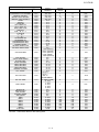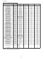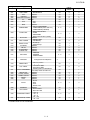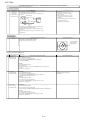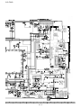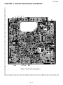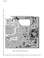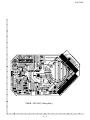
1
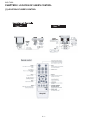
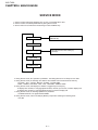
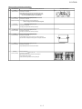
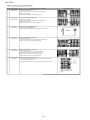
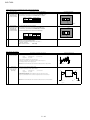
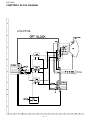
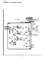
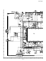
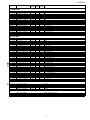
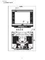
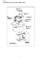
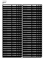
21G-FX10L SERVICE MANUAL S9914021GFX10L COLOUR TELEVISION Chassis No. GA8P Chassis No. GA6 MODEL 21G-FX10L In the interests of user safety (Required by safety regulations in some countries) the set should be restored to its original condition and only parts indentical to those specified should be used. CONTENTS Page IMPORTANT SERVICE SAFETY PRECAUTION ................................................................................................... 1-1 LOCATION OF USER’S CONTROL ...................................................................................................................... 2-1 INSTALLATION AND SERVICE INSTRUCTIONS ................................................................................................. 3-1 SERVICE MODE ..................................................................................................................................................... 4-1 ADJUSTMENT METHOD ........................................................................................................................................ 5-1 WAVEFORMS ......................................................................................................................................................... 6-1 CHASSIS LAYOUT ................................................................................................................................................. 7-1 BLOCK DIAGRAM .................................................................................................................................................. 8-1 DESCRIPTION OF SCHEMATIC DIAGRAM .......................................................................................................... 9-1 SCHEMATIC DIAGRAMS ......................................................................................................................................10-1 PRINTED WIRING BOARD ASSEMBLIES ........................................................................................................... 11-1 Parts Guide ELECTRICAL SPECIFICATIONS POWER INPUT............................AC 110-220 V, 50/60 Hz POWER RATING .....................................................89W PICTURE SIZE .............................1,239 cm2 (192sq inch) CONVERGENCE ............................................. Magnetic SWEEP DEFLECTION .................................. .. Magnetic FOCUS ......................................................... Electrostatic INTERMEDIATE FREQUENCIES Picture IF Carrier Frequency ...................... 45.75 MHz Sound IF Carrier Frequency ...................... 41.25 MHz Color Sub-Carrier Frequency ......................42.17 MHz (Nominal) AUDIO POWER OUTPUT RATING... ...................... 3.0 W(RMS) x 2pcs SHARP CORPORATION SPEAKER SIZE ........................................................ 9 x 5cm, 2pcs VOICE COIL IMPEDANCE .................16 ohm at 400 Hz ANTENNA INPUT IMPEDANCE VHF/UHF ........................................75 ohm Unbalanced TUNING RANGES VHF-Channels ................................................. 2 thru 13 UHF-Channels ................................................14 thru 69 CATV Channels ............................................. 1 thru 125 (EIA, Channel Plan U.S.A.) Specifications are subject to change without prior notice. This document has been published to be used for after sales service only. The contents are subject to change without notice. 21G-FX10L CHAPTER 1. IMPORTANT SERVICE SAFETY PRECAUTION Service Manual TV E Market 21G-FX10L IMPORTANT SERVICE SAFETY PRECAUTION Service work should be performed only by qualified service technicians who are thoroughly familiar with all safety checks and the servicing guidelines which follow: WARNING X-RADIATION AND HIGH VOLTAGE LIMITS 1. For continued safety, no modification of any circuit should be attempted. 2. Disconnect AC power before servicing. 3. Semiconductor heat sinks are potential shock hazards when the chassis is operating. 4. The chassis in this receiver has two ground systems which are separated by insulating material. The nonisolated (hot) ground system is for the B+ voltage regulator circuit and the horizontal output circuit. The isolated ground system is for the low B+ DC voltages and the secondary circuit of the high voltage transformer. To prevent electrical shock use an isolation transformer between the line cord and power receptacle, when servicing this chassis. 1. Be sure all service personnel are aware of the procedures and instructions covering X-radiation. The only potential source of X-ray in current solid state TV receivers is the picture tube. However, the picture tube does not emit measurable X-Ray radiation, if the high voltage is as specified in the "High Voltage Check" instructions. It is only when high voltage is excessive that Xradiation is capable of penetrating the shell of the picture tube including the lead in the glass material. The important precaution is to keep the high voltage below the maximum level specified. 2. It is essential that servicemen have available at all times an accurate high voltage meter. The calibration of this meter should be checked periodically. 3. High voltage should always be kept at the rated value −no higher. Operation at higher voltages may cause a failure of the picture tube or high voltage circuitry and;also, under certain conditions, may produce radiation in exceeding of desirable levels. 4. When the high voltage regulator is operating properly there is no possibility of an X-radiation problem. Every time a color chassis is serviced, the brightness should be tested while monitoring the high voltage with a meter to be certain that the high voltage does not exceed the specified value and that it is regulating correctly. 5. Do not use a picture tube other than that specified or make unrecommended circuit modifications to the high voltage circuitry. 6. W h e n t r o u b l e s h o o t i n g a n d t a k i n g t e s t measurements on a receiver with excessive high voltage, avoid being unnecessarily close to the receiver. Do not operate the receiver longer than is necessary to locate the cause of excessive voltage. SERVICING OF HIGH VOLTAGE SYSTEM AND PICTURE TUBE When servicing the high voltage system, remove the static charge by connecting a 10k ohm resistor in series with an insulated wire (such as a test probe) between the picture tube ground and the anode lead. (AC line cord should be disconnected from AC outlet.) 1. Picture tube in this receiver employs integral implosion protection. 2. Replace with tube of the same type number for continued safety. 3. Do not lift picture tube by the neck. 4. Handle the picture tube only when wearing shatterproof goggles and after discharging the high voltage anode completely. 1–1 21G-FX10L IMPORTANT SERVICE SAFETY PRECAUTION (Continued) BEFORE RETURNING THE RECEIVER (Fire & Shock Hazard) Before returning the receiver to the user, perform the following safety checks. 1. Inspect all lead dress to make certain that leads are not pinched or that hardware is not lodged between the chassis and other metal parts in the receiver. 2. Inspect all protective devices such as non-metallic control knobs, insulating materials, cabinet backs, adjustment and compartment covers or shields, isolation resistor-capacity networks, mechanical insulators, etc. 3. To be sure that no shock hazard exists, check for leakage current in the following manner. • Plug the AC cord directly into a 110~220 volt AC outlet, (Do not use an isolation transformer for this test). • Using two clip leads, connect a 1.5k ohm, 10 watt resistor paralleled by a 0.15μF capacitor in series with all exposed metal cabinet parts and a known earth ground, such as electrical conduit or electrical ground connected to earth ground. • Use an AC voltmeter having with 5000 ohm per volt, or higher, sensitivity to measure the AC voltage drop across the resistor. • Connect the resistor connection to all exposed metal parts having a return to the chassis (antenna, metal cabinet, screw heads, knobs and control shafts, escutcheon, etc.) and measure the AC voltage drop across the resistor. AII checks must be repeated with the AC line cord plug connection reversed. (If necessary, a nonpolarized adapter plug must be used only for the purpose of completing these check.) Any current measured must not exceed 0.5 milliamp. Any measurements not within the limits outlined above indicate of a potential shock hazard and corrective action must be taken before returning the instrument to the customer. DVM AC SCALE 1.5k ohm 10W TO EXPOSED METAL PARTS CONNECT TO KNOWN EARTH GROUND SAFETY NOTICE Many electrical and mechanical parts in television receivers have special safety-related characteristics. These characteristics are often not evident from visual inspection, nor can protection afforded by them be necessarily increased by using replacement components rated for higher voltage, wattage, etc. Replacement parts which have these special safety characteristics are identified in this manual; electrical components having such features are identified by " " and shaded areas in the Replacement Parts Lists and Schematic Diagrams. 1–2 For continued protection, replacement parts must be identical to those used in the original circuit. The use of substitute replacement parts which do not have the same safety characteristics as the factory recommended replacement parts shown in this service manual, may create shock, fire, X-radiation or other hazards. 21G-FX10L CHAPTER 2. LOCATION OF USER'S CONTROL Service Manual TV E Market 21G-FX10L [1] LOCATION OF USER'S CONTROL AV a AV AVa 2–1 21G-FX10L CHAPTER 3. INSTALLATION AND SERVICE INSTRUCTIONS Service Manual TV E Market 21G-FX10L INSTALLATION AND SERVICE INSTRUCTIONS Note: (1) When performing any adjustments to resistor controls and transformers use non-metallic screwdrivers or TV alignment tools. (2) Before performing adjustments, the TV set must be on at least 15 minutes. CIRCUIT PROTECTION HIGH VOLTAGE CHECK The receiver is protected by a 3.15A fuse (F701), mounted on PWB-A, wired into one side of the AC line input. High voltage is not adjustable but must be checked to verify that the receiver is operating within safe and efficient design limitations as specified checks should be as follows: X-RADIATION PROTECTOR CIRCUIT TEST After service has been performed on the horizontal deflection system, high voltage system, B+ system, test the X-Radiation protection circuit to ascertain proper operation as follows: 1. Apply 110~220V AC using a variac transformer for accurate input voltage. 2. Allow for warm up and adjust all customer controls for normal picture and sound. 3. Receive a good local channel. 4. Connect a digital voltmeter to C602 +ve and make sure that the voltmeter reads 20 ±1.1V. 5. Apply external 28.5V DC at C602 +ve by using an external DC supply, TV must be shut off. 6. To reset the protector, unplug the AC cord and make a short circuit between C602 -ve and C602 +ve. Now make sure that normal picture appears on the screen. 7. If the operation of the horizontal oscillator does not stop in step 5, the circuit must be repaired before the set is returned to the customer. 3–1 1. Connect an accurate high voltage meter between ground and anode of picture tube. 2. Operate receiver for at least 15 minutes at 110~220V AC line voltage, with a strong air signal or a properly tuned in test signal. 3. Enter the service mode and set Y-mute ON by using Service R/C. 4. The voltage should be approximately 26kV (at zero beam). If a correct reading cannot be obtained, check circuitry for malfunctioning components. After the voltage test, make Y-mute off to the normal mode. 21G-FX10L CHAPTER 4. SERVICE MODE Service Manual TV E Market 21G-FX10L SERVICE MODE 1. Service mode is switched by SERVICE key, CH UP + VOL DOWN when reset. 2. Service mode is cancelled by SERVICE key during Service mode. 3. Service mode can be switched to the following 5 modes via MENU key: First mode of service when entering by SERVICE key. Adjustment mode Setting mode First mode of service when entering by 2 local keys. Confirmation mode Option mode NVM Edit mode 4䋮During Service mode, AFT operation is prohibited. The setting data for PLL is always set to fo data. 5䋮During Service mode, the following user data are set to default value and stored as last memory. PICTURE䋯TINT䋯COLOR䋯BRIGHT䋯SHARP䋯COLOR TEMP. BASS䋯TREBLE䋯BALANCE䋯MTS䋯FAO䋯SPEAKER䋯ENERGY SAVE 6䋮During Service mode, OSD display for ON/OFF is toggled via [CH CALL] key. 䊶At display OFF condition, if changing adjustment data, channel, input source, it remains display OFF. 䊶At display OFF condition, if changing adjustment item, it returns to display ON. 7䋮During Service mode, the following operation are prohibited. CLOSED CAPTION䋯No signal BLUE SCREEN 8䋮During Service mode, sound is muted(only MTSIC) except when selecting the following items. V24, M01 4–1 21G-FX10L AUTO ADJUSTMENT H-VCO 1. When there is H-VCO auto adjustment key input at item H-VCO, auto adjustment will be implemented. 2. H-FREE (1chip) is set to 1. 3. H-OUT (1chip) is set by intelligent monitor output. 4. IM input becomes TIM input. 5. H-VCO (1chip) data is changed so that the number is 126 inside 8ms interval. 6. When adjustment is completed, OSD display and H-VCO auto adjustment data of EERPOM are updated. 7. H-FREE (1chip), intelligent monitor output, IM input mode are recovered. RF-AGC 1. If there is RF-AGC auto adjustment key input at item RF-AGC, auto adjustment will be implemented. 2. AGC-OUT (MONITOR(1chip)is set by intelligent monitor output. 3. IM input becomes AD input. 4. RF-AGC(1chip) is decreased from current RF-AGC value to 0, the maximum AFT input voltage is obtained. 5. RF-AGC(1chip) is increased until at the point of AFT input voltage is (max. 0.3V), adjustment is completed. 6. When adjustment is completed, OSD display and RFGC auto adjustment status in EEPROM are updated. 7. Intelligent monitor output, IM input mode are recovered. PIF-VCO 1. If there is PIF-VCO auto adjustment key input at item PIF- VCO, auto adjustment will be implemented. 2. VIF-DEF (1chip) is set to 1. 3. AFT output (1chip) is set by intelligent monitor output. 4. IM input becomes AD input. 5. VIF-VCO (1chip) is changed so the input voltage becomes 2.5V. 6. When adjustment is completed, OSD display and PIF-VCO auto adjustment status in EEPROM are updated. 7. VIF-DEF (1chip) intelligent monitor output, IM input mode are recovered. S-TRAP 1. If there is S-TRAP auto adjustment key input at item S-TRAP, auto adjustment will be implemented. 2. S-TRAP OUTPUT is set by intelligent monitor output. 3. IM input becomes AD input. 4. S-Trap (1chip) is set to the value of V45(S-TRAP ADJ Start). 5. S_Trap_Result is set to the value of V45(S-TRAP ADJ Start). 6. S-Trap (1chip) is increased until the minimum input voltage becomes minimum. 7. Wait 20ms before sampling the new_ AD_data. 8. When adjustment is completed, OSD display and S-TRAP auto adjustment status in EEPROM are updated. 9. S-TRAP (1chip) intelligent monitor output, IM input mode are recovered. 4–2 21G-FX10L CHAPTER 5. ADJUSTMENT METHOD Service Manual TV E Market 21G-FX10L Memory Map Data Caution: To get into the service mode, one of the ways is press direct key for service items. There is three stage of Service Mode data First stage data from V01 ~ M01 to go into second stage of service mode data, press MENU key Second stage data from F01 ~ F160 to go into third stage of service mode data, press MENU key Third stage data from O01 ~ O31 Adjustmet Mode (First Stage) V25 V26 DATA LENGTH 0~127 0~127 0~127 0~255 0~63 0~63 0~7 0~31 0~127 0~63 -7~+7 -15~+15 -31~+31 0~63 0~255 0~255 0~255 0~127 0~127 0~127 0~127 0~255 0~2 0~127 (O20=0) 0~255 (O20=1) 0~7 0~127 INITIAL DATA 127 64 64 128 41 41 4 16 127 32 0 0 0 32 127 127 127 64 64 64 64 32 0 127 255 4 64 VS-CORRECT V27 0~63 36 VS-CORRECT50 V28 -13~+13 0 0 FIX V LINEARITY V29 0~63 35 37 *FIX V LINEARITY50 PARABOLA PARABOLA50 TRAPEZIUM TRAPEZIUM50 H-SIZE H-SIZE50 UPPER CORNER UPPER CORNER50 LOWER CORNER LOWER CORNER50 ANGLE ADJ ANGLE ADJ50 BOW ADJ BOW ADJ50 S-TRAP ADJ START S-TRAP STOP MTS-ATT V30 V31 V32 V33 V34 V35 V36 V37 V38 V39 V40 V41 V42 V43 V44 V45 V46 M01 -13~+13 0~63 -13~+13 0~63 -13~+13 0~63 -13~+13 0~63 -13~+13 0~63 -13~+13 0~63 -13~+13 0~63 -13~+13 0~127 0~127 0~15 0 32 0 32 0 32 0 32 0 32 0 31 0 31 0 25 95 10 0 32 0 32 0 32 0 32 0 32 0 31 0 31 0 25 95 10 FIX ADJ FIX ADJ FIX ADJ FIX ADJ FIX ADJ FIX ADJ FIX ADJ FIX FIX FIX FIX EEPROM ITEMS OSD SUB-CON SUB-TINT SUB-COL SUB-BRI SUB-SHP-PRE SUB-SHP-OVER V-SHIFT H-SHIFT RF-AGC V-SIZE V-SHIFT50 H-SHIFT50 V-SIZE50 VIF-VCO R-CUT G-CUT B-CUT R-DRI B-DRI SUB-COLOR-YUV SUB-TINT-YUV CC-POS SCREEN CUT OFF V01 V02 V03 V04 V05 V06 V07 V08 V09 V10 V11 V12 V13 V14 V15 V16 V17 V18 V19 V20 V21 V22 V23 SUB-VOL V24 H-VCO S-TRAP Auto Adjustment Item Ԙ H-VCO , ԙ RF-AGC, Ԛ VIF-VCO, ԛ S-TRAP Remark: * Initial Data different with Setting Data 5–1 SETTING DATA FIX/ADJ/AUTO 127 64 64 128 40 24 4 16 127 32 0 0 0 32 127 127 127 64 64 64 64 32 0 115 4 64 ADJ ADJ ADJ ADJ *FIX *FIX ADJ ADJ AUTO ADJ FIX FIX FIX AUTO ADJ ADJ ADJ ADJ ADJ FIX FIX ADJ FIX 26 *FIX REMARK *FIX AUTO AUTO ADJUST IF NECESSARY TO IMPROVE ADJUST IF NECESSARY TO IMPROVE 21G-FX10L SETTING MODE (Second Stage) EEPROM ITEMS OSD ABCL-Gain SHP-AV-PRE SHP-YUV-PRE SHP-P-PRE SHP-N3-PRE SHP-AV-OVER SHP-YUV-OVER SHP-P-OVER SHP-N3-OVER SHP ANT-ON II OFFSET RGB-CLIP E-SAVE F01 F02 F03 F04 F05 F06 F07 F08 F09 F10 F11 F12 FAO-VOL F13 VIF-G YDL-TV YDL-TV-P YDL-TV-N3 YDL-AV YDL-AV-P YDL-AV-N3 YDL-YUV TINT-AV COL-AV COL-P COL-N3 R-R R-B B-R B-B GAMMA BS-D BS-C SL-TV SL-AV SL-YUV AFC2 VD-TV VD-AV VD-YUV AS-TV AS-AV AS-YUV FBP-TV FBP-AV FBP-YUV C.Clip Level CP CC LEVEL OSD POS-H OSD POS-V50 OSD POS-V60 OFFSET-ADJ-COLOR OFFSET-ADJ-TINT WAIT˴MD˴TIMER R-CUT-YUV G-CUT-YUV B-CUT-YUV R-DRI-YUV B-DRI-YUV F14 F15 F16 F17 F18 F19 F20 F21 F22 F23 F24 F25 F26 F27 F28 F29 F30 F31 F32 F33 F34 F35 F36 F37 F38 F39 F40 F41 F42 F43 F44 F45 F46 F47 F48 F49 F50 F51 F52 F53 F54 F55 F56 F57 F58 F59 DATA LENGTH 0/1 -16~+16 -16~+16 -31~+31 -31~+31 -16~+16 -16~+16 -31~+31 -31~+31 -15~0 0/1 0~63 0~127 (O20=0) 0~255 (O20=1) 0~7 0~7 0~7 0~7 0~7 0~7 0~7 0~7 -32~+32 -32~+32 -31~+31 -31~+31 -32~+32 -32~+32 -32~+32 -32~+32 0~3 0~3 0~3 0~7 0~7 0~7 0~3 0~7 0~7 0~7 0/1 0/1 0/1 0/1 0/1 0/1 0/1 0/1 0~31 0~31 1~55 1~50 -32~+32 -32~+32 0/1 -63~+63 -63~+63 -63~+63 -63~+63 -63~+63 Remark: * Initial Data different with Setting Data 5–2 INITIAL DATA 0 0 0 0 0 0 0 0 0 -10 0 30 120 246 5 5 5 5 5 5 5 0 +6 0 +24 0 +3 -2 -8 +6 1 0 0 2 2 0 0 5 7 1 1 1 0 0 0 0 0 1 0 0 38 23 +10 +2 1 0 0 0 0 0 SETTING DATA FIX/ADJ/AUTO 0 -10 0 0 0 -10 0 0 0 -10 0 30 81 7 5 5 5 5 5 4 0 -16 +10 +24 0 +7 0 -20 +9 3 0 0 1 2 0 1 1 2 0 1 1 0 0 0 0 0 1 0 14 48 32 +15 +9 1 0 0 0 0 0 FIX *FIX FIX FIX FIX *FIX FIX FIX FIX FIX FIX FIX *FIX *FIX FIX FIX FIX FIX FIX *FIX FIX *FIX *FIX FIX FIX *FIX *FIX *FIX *FIX *FIX FIX FIX *FIX FIX FIX *FIX *FIX *FIX *FIX FIX FIX FIX FIX FIX FIX FIX FIX FIX *FIX *FIX *FIX *FIX *FIX FIX FIX FIX FIX FIX FIX 21G-FX10L SETTING MODE (Second Stage) EEPROM ITEMS OSD ABCL GOFFSET i CONTRAST CONTRAST YUV OFFSET BRIGHT OFFSET BRIGHT AV2 OFFSET BRIGHT YUV OFFSET TRAP TRAP-P TRAP-N3 AFC1-Gain-TV AFC1-Gain-AV AFC1-Gain-YUV OM-DET 㧮㧿㧙㧳㨍㨕㨚 C-ANGLE 㨂㧙㧰㧸 㨁㧙㧰㧸 AS-SPEED-DN AS-SPEED-UP CR-PEDESTEL-ADJ CB-PEDESTEL-ADJ SIF-BPF-WIDE SIF-BPF-WIDE-LOW SIF-BPF-WIDE-HIGH F60 F61 F62 F63 F64 F65 F66 F67 F68 F69 F70 F71 F72 F73 F74 F75 F76 F77 F78 F79 F80 F81 F82 COL-SYSTEM F83 Pow-Storage SIF45 GAIN DOWN S-TRAP OFF BASS OFFSET MID1 OFFSET MID2 OFFSET MID3 OFFSET TREBLE OFFSET AVL LEVEL F84 F85 F86 F87 F88 F89 F90 F91 F92 AVL OPTION F93 AU-ATT AMP F94 OSD LEVEL F95 R MTX UP MATRIX ADJ SAP LEVEL STEREO SENS SAP SENS MER MEL1 MEL2 MEL3 MEL4 MEL5 MEL6 S-St-Point F96 F97 F98 F99 F100 F101 F102 F103 F104 F105 F106 F107 F108 DATA LENGTH -63~+63 -63~+63 -63~+63 -15~+15 -63~+63 0~3 0~3 0~3 0~3 0~3 0~3 0/1 0~2 0/1 0~3 0~3 0/1 0/1 0~15 0~15 0~7 0/1 0/1 0: 11XX (AUTO) 1: 0011 (PAL-M) 2: 0111 (PAL-N) 3: 0110 (N358) 4: 10XX (AUTO1) 0/1 0/1 0/1 -4~+4 -4~+4 -4~+4 -4~+4 -4~+4 0~3 0: fix to 0 1: fix to 1 2: AVL in SOUND MENU 0 (0dB)/1(3dB) 0: 10% 1: 30% 2: 50% 3: 70% 4: 90% 0/1 0~3 0/1 0/1 0/1 0~255 0~255 0~255 0~255 0~255 0~255 0~255 0~60 Remark: * Initial Data different with Setting Data 5–3 INITIAL DATA 0 0 0 +1 0 2 2 2 0 3 3 0 0 0 0 0 0 0 8 8 3 0 0 SETTING DATA FIX/ADJ/AUTO 0 0 0 +4 0 0 2 2 0 3 3 0 0 0 0 0 0 0 8 8 1 0 0 FIX FIX FIX *FIX FIX *FIX FIX FIX FIX FIX FIX FIX FIX FIX FIX FIX FIX FIX FIX FIX *FIX FIX FIX 3 3 FIX 1 0 1 0 0 0 0 0 0 1 0 0 0 0 0 0 0 1 FIX FIX *FIX FIX FIX FIX FIX FIX *FIX 2 1 *FIX 0 1 *FIX 3 3 FIX 0 0 0 0 0 70 150 156 163 165 170 180 21 0 0 0 0 0 70 150 156 163 165 170 180 21 FIX FIX FIX FIX FIX FIX FIX FIX FIX FIX FIX FIX FIX 21G-FX10L SETTING MODE (Second Stage) EEPROM ITEMS OSD ABCL G i S-Sp-Point S-Step CONT NEWS CONT MUSIC CONT MOVIE BRIGHT NEWS BRIGHT MUSIC BRIGHT MOVIE COL NEWS COL MUSIC COL MOVIE SHARP NEWS SHARP MUSIC SHARP MOVIE SURR NEWS SURR MUSIC SURR MOVIE TREBLE NEWS TREBLE MUSIC TREBLE MOVIE BASS NEWS BASS MUSIC BASS MOVIE EQ BASS NEWS EQ BASS MUSIC EQ BASS MOVIE EQ MID1 NEWS EQ MID1 MUSIC EQ MID1 MOVIE EQ MID2 NEWS EQ MID2 MUSIC EQ MID2 MOVIE EQ MID3 NEWS EQ MID3 MUSIC EQ MID3 MOVIE EQ TRE NEWS EQ TRE MUSIC EQ TRE MOVIE S-BOOST NEWS S-BOOST MUSIC S-BOOST MOVIE CORNER UP-LOW EN BOW/ANGLE-ON/OFF SHP-NR-OFFSET V-FREE60 TAKEOFF TV STRAP OFFSET RGB MUTE TIME H-BLK LEFT H-BLK RIGHT F109 F110 F111 F112 F113 F114 F115 F116 F117 F118 F119 F120 F121 F122 F123 F124 F125 F126 F127 F128 F129 F130 F131 F132 F133 F134 F135 F136 F137 F138 F139 F140 F141 F142 F143 F144 F145 F146 F147 F148 F149 F150 F151 F152 F153 F154 F155 F156 F157 F158 H-STOP DELAY F159 SYS MUTE F160 DATA LENGTH 0~60 0~60 0~60 0~60 0~60 -30~+30 -30~+30 -30~+30 -30~+30 -30~+30 -30~+30 -30~+30 -30~+30 -30~+30 0(OFF)/1(ON) 0(OFF)/1(ON) 0(OFF)/1(ON) -10~+10 -10~+10 -10~+10 -10~+10 -10~+10 -10~+10 -10~+10 -10~+10 -10~+10 -10~+10 -10~+10 -10~+10 -10~+10 -10~+10 -10~+10 -10~+10 -10~+10 -10~+10 -10~+10 -10~+10 -10~+10 0(OFF)/1(ON) 0(OFF)/1(ON) 0(OFF)/1(ON) 0/1 0(OFF)/1(ON) -15~0 0/1 0/1 -16~+16 0~8 0~7 0~7 0: 5ms 1: 10ms 2: 15ms 3: 20ms 0/1 Remark: * Initial Data different with Setting Data 5–4 INITIAL DATA 60 7 40 50 60 0 0 0 0 0 +10 -10 0 +5 0 0 0 -10 0 +5 -5 0 +10 0 0 0 0 0 0 0 0 0 0 0 0 0 0 0 0 1 1 1 1 0 1 0 0 0 0 0 SETTING DATA FIX/ADJ/AUTO 60 7 40 50 60 0 0 0 0 0 +10 -10 0 +5 0 0 0 -10 0 +5 -5 0 +10 0 0 0 0 0 0 0 0 0 0 0 0 0 0 0 0 1 1 1 1 0 1 0 0 1 0 3 FIX FIX FIX FIX FIX FIX FIX FIX FIX FIX FIX FIX FIX FIX FIX FIX FIX FIX FIX FIX FIX FIX FIX FIX FIX FIX FIX FIX FIX FIX FIX FIX FIX FIX FIX FIX FIX FIX FIX FIX FIX FIX FIX FIX FIX FIX FIX *FIX FIX *FIX 1 1 FIX 0 0 FIX 21G-FX10L Setting Mode (Third stage) Data O01 O02 O03 O04 O05 O06 O07 O08 O09 O10 O11 O12 O13 O14 O15 O16 O17 O18 O19 O20 O21 O22 O23 O24 O25 O26 O27 O28 O29 O30 O31 OPTION FUNCTION Description Range INITIAL DATA Setting Data 0/1 0 0 0/1 0/1 0/1 0/1 1 0 0 1 0 1 0 1 0/1 1 1 0/1 1 0 0…2 1 0 0…3 1 3 0/1 1 1 0/1 0 0 0/1 1 1 0/1 0/1 0/1 0/1 1 0 0 0 0 0 0 0 0…2 0 1 7 1 0/1 1 0 0/1 0 0 0/1 1 1 0/1 0/1 0/1 0/1 0/1 0 1 0 1 1 0 1 0 1 1 0…3 3 3 0/1 1 0 0/1 0 1 0…2 0 0 0/1 0 0 0 : ALPS 1 : MATSUSHITA FAO DIS/ENA * PON-CH DIS/ENA ANTENNA BOOSTER DIS/ENA AV DIS/ENA 0 : AV1 AV2 1 : AV2 MTS DIS/ENA 0 : without COMPONENT COMPONENT 1 : COMPONENT (share with AV1) 2 : COMPONENT (individual) 0 : Without Sound Menu TONE-CTRL 1 : TONE 2 : EQUALIZER 3 : Without Sound Menu (GA8P) AUTO-OFF DIS/ENA 0 : Standby Mode LAST POWER 1 : Last Memory 0 : No Set Up SETUP-FLAG 1 : AUTO Set Up AV MODE DIS/ENA MP-IN DIS/ENA S-BOOSTER DIS/ENA FORCE-COL DIS/ENA 0 : ENGLISH INIT-LANG 1 : SPANISH 2 : PORTUGUESE LNA TUNER LANG-SEL Portuguese/French/Spanish 0 : CH ٌ/ٖ, VOL+/1: / , / 0 : 7-bit volume table VOL-TABLE 1 : 8-bit volume table 0 : EZ Setup Same as GA6 Brazil AUTO-JUDGEMENT 1: EZ Setup Same as GA6 LAG WHITE-OUT DIS/ENA H-SYNC JUDGE DIS/ENA CHSET COLOR DIS/ENA DEMO DIS/ENA FLAT DIS/ENA 0 : No AV 1 : Rear F/R-AV 2 : Front 3 : Rear & Front SPEAKER DIS/ENA 0 : Old Vol-Table VOL-CURVE 1 : New Vol-Table 0 : -105 ~ 0 CONTRAST TABLE 1 : -60 ~ 0 2 : -30 ~ 0 0 : -60 ~ +60 BRIGHTNESS TABLE 1 : -30 ~ +30 ARROW-KEY * POWER ON BY CH-UP / DOWN KEY. 5–5 0…7 21G-FX10L ADJUSTMENT PRECAUTION : Make sure TV Set is in "NORMAL CONDITION" before switch to Service Mode for Adjustment. PIF ADJUSTMENT CHECKING NO 1 ADJUSTMENT POINT RF-AGC TAKE OVER POINT ADJUSTMENT (I2C BUS CONTROL) (AUTO & MANUAL ADJ) ADJUSTMENT CONDITION/PROCEDURE (1) Receive the "US 10 CH HALF Color Bar" signal. Signal Strength: 56 ± 1dBμV (75 ohm open) (2) Connect the oscilloscope to JA402 (Tuner's AGC Terminal) as shown in figure 3-1. + OSCILLOSCOPE 0.1V JA402 + BIAS BOX TV SET Bias Box : about 4.5V Fig. 3-1 (3) Call V09 in service mode. Adjust the V09 bus data to obtain the Tuner output pin drop 0.1V below maximum voltage. (4) Change the antenna input signal to 63 ~ 67dBμV, and make sure there is no noise. (5)Turn up the input signal to 90 ~ 95 dBμV to be sure that there is no cross modulation beat. WAVEFORM OR OTHERS * for Auto ADJ 1)Receive "NTSC COLOUR BAR" signal signal strength : 56 ± 1 dBμV (75 ohm open). 1) Go to service mode. 2) Go to service data V09 , press R/C to operate "Auto-AGC" key and confirm the OK display on the screen 3) If appear red display with NG sign, increase data some step and please repeat step 2. 4) Proceed step 4 & 5 in manual mode. FOCUS ADJUSTMENT NO 1 ADJUSTMENT POINT FOCUS ADJUSTMENT CONDITION / PROCEDURE (1) Receive US4 CH LION HEAD Signal (NTSC 60 Hz). (2) Press RESET to set Picture NORMAL condition. (3) Adjust the focus control to get the best focusing. WAVEFORM OR REMARKS Focusing Point (middle of center and edge of monoscope pattern) H-VCO, VIF-VCO & S-TRAP fo ADJUSTMENT NO ADJUSTMENT POINT 1 H-VCO ADJ (I2C BUS CONTROL) (AUTO & MANUAL ADJ) ADJUSTMENT CONDITION / PROCEDURE (Manual Adj) (1) In No signal (RASTER) condition. (2) Go to service mode, choose service data V25. (3) Connect oscilloscope to IC801 pin13 (H-OUT), adj V25 until freq become 15.735 ± 0.2KHz. WAVEFORM OR OTHERS (Auto Adj) (1) In No signal (RASTER) condition. (2) Go to service mode. (3) Choose service data V25, by pressing R/C "AUTO H-VCO" key, OSD will appear "OK" at screen. (4) If appear "NG" pls repeat step 3. 2 VIF-VCO ADJ (I2C BUS CONTROL) (AUTO & MANUAL ADJ) 3 S-TRAP fo ADJ (I2C BUS CONTROL) (AUTO & MANUAL ADJ) (Manual Adj) (1) In No signal (RASTER) condition. (2) Go to service mode, choose service data V14 (3) Connect oscilloscope to IC801 pin7 (AFT), adj V14 until voltage become 2.5 ± 0.5 V DC (Checking spec : 2.50 ± 1.5 V) (Auto Adj) (1) In No signal (RASTER) condition. (2) Go to service mode, choose service data V14. (3) Press the R/C "AUTO PIF-VCO" key, OSD will appear "OK" at screen. (4) If appear "NG" pls repeat step 3. (Manual ADJ) (1) In No signal (RASTER) condition. (2) Go to service mode, choose service data V26. (3) Connect oscilloscope to TP 801 or IC801 pin 30, adj V26 until voltage become Min (below 5 V). (Auto Adj) (1) In No signal (RASTER) condition. (2) Go to service mode, choose service data V26. (3) Press the R/C "AUTO S-TRAP" key, OSD will appear "OK" at screen. (4) If appear "NG" pls repeat step 3. 5–6 *NOTE: This adjustment must be done after aging at least 3 minutes. 21G-FX10L HORIZONTAL ,VERTICAL,DEFLECTION LOOP ADJUSTMENT (1) NO 1 ADJUSTMENT POINT V-SHIFT (I2C BUS CONTROL) ADJUSTMENT CONDITION / PROCEDURE (1) Receive US4 CH LION HEAD Signal (NTSC 60 Hz). (2) Choose the service data V07. (3) Adjust V07 to align the center of the screen to the geometric center of CRT. Note: B line (Monoscope middle line) must same or nearest higher position to the A mark (Tube middle mark),refer to the attach drawing. WAVEFORM OR OTHERS A B Figure OK 2 OK NG V-SIZE (I2C BUS CONTROL) (1) Receive US4 CH LION HEAD Signal (NTSC 60 Hz). (2) Choose the service data V10. (to be done after V-shift adj) (3) Adjust V10 bus data until the overscan become 10 ± 2.5 %. Caution 1: Pls aging TV more than 10 minutes before adjustment 3 V-LINEARITY (I2C BUS CONTROL) (1) Receive US4 CH LION HEAD Signal (NTSC 60 Hz). (2) Choose the service data V29. (3 )Already preset. (Adjust this unless the linearity is achieved.) 4 VS CORRECTION (I2C BUS CONTROL) (1) Receive US4 CH LION HEAD Signal (NTSC 60 Hz). (2) Choose the service data V27. (3 )Already preset. (Adjust this unless the linearity is achieved.) 5 H-SHIFT (I2C BUS CONTROL) (1) Receive US4 CH LION HEAD Signal (NTSC 60 Hz). (2) Choose the service data V08. (3) Adjust the V08 bus data to have a balance position to spec of A=B (as attach drawing). (4) If cannot make it to A=B, adjust from the best point so that A slightly smaller than B. 6 H-SIZE (I2C BUS CONTROL) (1) Receive US4 CH LION HEAD Signal (NTSC 60 Hz). (2) Choose the service data V35 (3) Adjust V35 bus data until the overscan becomes 10 ± 2.5 %. 7 PARABOLA (I2C BUS CONTROL) (1) Receive CrossHatch Pattern Signal (NTSC 60 Hz). (2) Choose the service data V31 Adjust the 2nd vertical line from the right end of the crosshatch pattern so that the middle 4 blocks are straight. (3) Make sure both left / right of 2nd vertical line at optimum point 5–7 A B 21G-FX10L HORIZONTAL ,VERTICAL,DEFLECTION LOOP ADJUSTMENT (2) NO 8 ADJUSTMENT POINT UPPER CORNER (I2C BUS CONTROL) ADJUSTMENT CONDITION / PROCEDURE (1) Receive CrossHatch Pattern Signal (NTSC 60 Hz). (2) Choose the service data V37 (3) Adjust the 2nd upper vertical line from the right end of the crosshatch pattern so that the upper line are straight. (4) Make sure both left / right of 2nd vertical line at optimum point 9 LOWER CORNER (I2C BUS CONTROL) (1) Receive CrossHatch Pattern Signal (NTSC 60 Hz). (2) Choose the service data V39 (3) Adjust the 2nd lower vertical line from the right end of the crosshatch pattern so that the bottom line are straight. (4) Make sure both left / right of 2nd vertical line at optimum point 10 BOW-ADJ (I2C BUS CONTROL) (1) Receive CrossHatch Pattern Signal (NTSC 60 Hz). (2) Choose the service data V43 BOW ADJ (3) Adjust the 2nd vertical line from the end of the crosshatch pattern until line is straight. WAVEFORM OR OTHERS H-BOW 11 ANGLE ADJ (I2C BUS CONTROL) (1) Receive CrossHatch Pattern Signal (NTSC 60 Hz). (2) Choose the service data V41 (3) Adjust the 2nd vertical line from the end of the crosshatch pattern line is straight (4) Make sure both left / right of 2nd vertical line at optimum point 12 TRAPEZIUM (I2C BUS CONTROL) (1) Receive CrossHatch Pattern Signal (NTSC 60 Hz). (2) Choose the service data V33 (3) Adjust the 2nd vertical line from the right end of the crosshatch pattern so that the D1 (center area of the second vertical line - edge of screen) and D2 (top area of the second vertical line - edge of screen) are same. (4) Make sure both left / right of 2nd vertical line at optimum point 13 FINAL INSPECTION OF (1) Receive CrossHatch Pattern Signal (NTSC 60Hz). ADJUSTMENT (2) Please make sure picture distortion (overall picture quality) must be balance at optimum point TOP / BOTTOM at LEFT / RIGHT corner. (3) If NG, please RE-ADJUST follow step 7 to 13 or adjust at NG position to get best picture quality A1 D2 D2 D1 D1 A2 D1 A1 B1 B2 D2 C1 C2 OVERALL PICTURE QUALITY MUST BE BALANCE AT OPTIMUM POINT ( LEFT & RIGHT ) 5–8 A1 ~ ~ ~ B1 ~ ~ C1 ~ D1 = A2 B2 C2 D2 21G-FX10L CLOSED CAPTION ADJUSTMENT NO ADJUSTMENT POINT 1 CLOSED CAPTION SET UP ADJUSTMENT CONDITION / PROCEDURE (1) Receive US4 CH LION HEAD Signal (NTSC 60 Hz) (2) Go to service mode, choose service data V22. (3) Adjust the V22 bus data to have a balance position to spec of A=B (4) After the left and right symmetrical then V22 data reduce 5 step WAVEFORM OR OTHERS A B SCREEN, WHITE BALANCE, SUB-BRIGHTNESS & SUB-CONTRAST ADJUSTMENT(1) NO 1 ADJUSTMENT POINT SCREEN ADJUSTMENT (I2C BUS CONTROL) ADJUSTMENT CONDITION / PROCEDURE (1) Set the service data before adjust CRT cutoff as follows: a) V01 : 127 b) V04 : 127 c) V15 : 127 d) V16 : 127 e) V17 : 127 f) V18 : 64 g) V19 : 64 WAVEFORM OR OTHERS NOTE: R/C key (Hex) A9 69 E9 19 99 59 Service data R-cutoff up R-cutoff down G-cutoff up G-cutoff down B-cutoff up B-cutoff down (2) Receive the window pattern or US4 CH LION HEAD Signal (NTSC 60 Hz) (3) Go to service mode, get in Y-mute by R/C and set V23 to "1" (4) Adjust the Screen so that cut-off line appear in low bright, then judge that whether the cut-off data appear in Red or Green or Blue color, in this condition between V15 = R-CUTOFF, V16=G-CUTOFF & V17= B-CUTOFF, fix the data of the color appear in cut-off line and adj the other two cut-off line so that cut-off line color become white. (5)Turn the screen VR of FBT so that cut-off line just disappear and use R/C to set V23 to "0". Next disable the Y-Mute so that the picture appear in normal mode 2 WHITE BALANCE ADJ (1)WHITE (HIGH BEAM) (to be done after screen First use Minolta Color Analyzer CA100, let the gun point at Dark White position adj) (as drawing attach), Adj V04 until LUMINANCE Y become 5 cd/m2, then let the gun (I2C BUS CONTROL) point at White position ( as drawing attach), Adj V01 until LUMINANCE Y (CH 23 50IRE become: 150 cd/m2. WINDOW PATTERN) Adj the V18(R DRIVE) , V19(B DRIVE) until the axis of color temperature become 10700° White Dark White X : 0.278 , Y : 0.280 (2) DARK WHITE (LOW BEAM) Let the gun point at Dark White position, if the color temperature data shift away from the data adjusted in Item 1 Screen adjustment, adjust V15,V16,V17. Please fix the first colour appears in Screen adj item step (4) is fixed, adj the other two so that to obtain the similar axis as above ** Repeat step 1 & 2 to get a regulated position 5–9 50% WHITE *Note : Use RF CH23 50IRE window pattern 21G-FX10L SCREEN, WHITE BALANCE, SUB-BRIGHTNESS & SUB-CONTRAST ADJUSTMENT(2) NO 3 ADJUSTMENT POINT SUB-BRIGHTNESS (to be done after screen, white balance adj) (I2C BUS CONTROL) ADJUSTMENT CONDITION / PROCEDURE (1) In CH 23 50IRE window pattern signal condition. (2) Using Minolta Color Analyzer CA-100, let the gun point atDark White position (as attach drawing), adjust V04 Bus data until BRIGHTNESS Y = 1.5cd/m2 Service Mode Enable Disable WAVEFORM OR OTHERS US14 Luminance Tolarance (cd/m2) (cd/m2) Upper Limit Lower Limit 1.5 +0.5 -0.5 1.5 +1.5 -0.5 Dark White 4 SUB-CONTRAST (to be done after screen, white balance adj, sub-brightness adj) (I2C BUS CONTROL) (1) In CH 23 50IRE window pattern signal condition. (2) Using Minolta Color Analyzer CA-100, let the gun point atWhite position (as attach drawing), adjust V01 Bus data until BRIGHTNESS Y = 150cd/m2 ** NOTE: Allowable Data for V01 >=90, even Y can't match the spec Service Mode Enable Disable 5 US14 Luminance Tolarance (cd/m2) (cd/m2) Upper Limit Lower Limit 150.0 +10 -10 150.0 +10 -10 White BEAM CURRENT CHECK (1) Receive US 4 CH LION HEAD Signal (NTSC 60 Hz). (2) Press R/C to set Picture NORMAL condition. (3) Connect the DC miliammeter between TP 603 ( + ) & TP 602 ( - ) (Full Scale: 3mA Range). (4) Beam current must be within : 1000 ± 100μA NTSC CHROMA ADJUSTMENT NO 1 ADJUSTMENT POINT SUB-TINT ADJUSTMENT CONDITION / PROCEDURE (1) Receive the "US 10 CH HALF Color Bar" signal. (2) Connect the oscilloscope to JA410 or TP853 BLUE-OUT WAVEFORM OR REMARKS (I2C BUS CONTROL) Range Sweep time : 500mV/Div (AC) : 10 sec/Div (Use Probe 10:1) (3) Select the service data V02 . On Y-mute using the R/C. (4) Adjust the V02 (Sub tint) data to obtain the waveform as shown in Figure 1.1 (B-Amp Base (TP853) must be in stepping level) *REMARK : PLEASE MAKE SURE USE RF SIGNAL DURING SUB TINT ADJUSTMENT Fig 1-1 2 SUB COLOR (I2C BUS CONTROL) (to be done after sub tint adj) (1) Receive the "US 10 CH HALF Color Bar" signal. (2) Make the image normal with the remote controller. (3) Connect the oscilloscope to JA401 (TP851) RED-OUT. Range Sweep time : 500mV/Div (AC) : 10 sec/Div ( Use Probe 10:1) (4) Select the service data V03. Adjust the V03 (Sub color) data to obtain the waveform adjustment shown in Fig. 1-2. (5) Fig 1.2 waveforms shows that the 75% white & red portions of color bar at the same level Cy G 100% WHITE *REMARK : PLEASE MAKE SURE USE RF SIGNAL DURING SUB COLOUR ADJUSTMENT W Y Fig 1-2 5 – 10 Mg R B 21G-FX10L PROTECTOR OPERATION CHECKING NO 1 ADJUSTMENT POINT 2 OTHER PROTECTOR H, V PROTECTOR ADJUSTMENT CONDITION / PROCEDURE (1) Receive US 4 CH LION HEAD Signal (NTSC 60 Hz). (2) Connect output of Bias Box to D602 cathode (C602 positive). (3) Set voltage of Bias Box to 18V and make sure the protector is not working. (4) Set voltage of Bias Box to 28.5V. Make sure the protector is functioned, horizontal oscilation stop and picture disappear. (5) Pull out the AC cord at least 4 second before plugging in again (to make sure ohm -COM has been reset) for the set to recover from protector mode WAVEFORM OR OTHERS (1) Once finish rectified Electrolytic Capacitor short testing in + B line, check all possible damaged components on +B line. (Use random selected set for inspection) A/V INPUT & OUTPUT CHECKING NO 1 ADJUSTMENT POINT VIDEO AND AUDIO OUTPUT CHECK ADJUSTMENT CONDITION / PROCEDURE (1) Receive the "US 10 CH HALF Color Bar" signal. (2) Terminate the Video output with a 75 ohm impedance. ( At signal is standard Color Bar Y/C=1/1, 87.5% Mod.) Make sure the output is as specified (1.0 Vp-p ± 3 dB). (3) Terminate the Audio output with a 47K ohm impedance. ( 400 Hz 100 % Mod. 47 k ohm, VOL Max. ) Set volume to max, make sure the O/P is as specified (2.5 Vp-p ± 0.5Vp-p) . . 2 VIDEO AND AUDIO INPUT CHECK 3 HEADPHONE CHECK (1) Using the INPUT key on the remote controller, make sure that the modes change in order of TV, INPUT1,INPUT2 & TV again and the video & audio output are according to the input terminal for each mode. (2) Video cross-talk INPUT to TV checking : a) When connect INPUT1 input, check TV also b) When connect INPUT2 input, check TV also (1) Receive "US 4 CH LION HEAD Signal ( NTSC 60 Hz )" signal. (2) Maximum volume , and check the headphone output with 400Hz sound and no sound output from speaker. 5 – 11 WAVEFORM OR OTHERS 21G-FX10L FUNCTION OPERATION CHECKING (VIDEO & AUDIO) (1) NO 1 E ADJUSTMENT CONDITION / PROCEDUR ADJUSTMENT POINT (1) Receive "US 4 CH LION HEAD Signal (NTSC 60 Hz)" signal. PICTURE Key (2) Press to Menu mode, then select Picture Mode and set to select CONTRAST. (3) Press Volume Up/Down key to check whether the CONTRAST effect is OK or not. 2 COLOUR Key 3 BRIGHTNESS Key 4 TINT Key 5 SHARPNESS Key 6 RESET KEY (1) Receive the "US 10 CH HALF Color Bar" signal (2) Press to Menu mode, then select Picture Mode and set to select COLOUR. (3) Press Volume Up/Down key to check whether the COLOUR effect is OK or not. (1) Receive "US 4 CH LION HEAD Signal (NTSC 60 Hz)" signal. (2) Press to Menu mode, then select Picture Mode and set to select BRIGHTNESS. (3) Press Volume Up/Down key to check whether the BRIGHTNESS effect is OK or not (1) Receive the "US 10 CH HALF Color Bar" signal (2) Press to Menu mode, then select Picture Mode and select TINT. (3) Press Volume Up/Down key to check TINT, UP for GREEN direction and DOWN for RED direction whether is OK or not. (1) Receive "US 4 CH LION HEAD Signal (NTSC 60 Hz)" signal. (2) Press to Menu mode, then select Picture Mode and set to select SHARPNESS. (3) Press Volume Up/Down key to check whether the SHARPNESS effect is OK or NOT. (1) Once in Picture Mode , and the RESET Key is pressed. all the setting will be present to normal setting. PICTURE COLOUR BRIGHTNESS TINT SHARP PICTURE NR COLOR TEMP 7 COLOR TEMP WAVEFORM OR REMARKS *NOTE : In RESET Mode,when press RESET key, will appear RESET OSD and all setting set to normal. 60 0 0 0 0 OFF Mid (1) Receive US 4 CH LION HEAD Signal ( NTSC 60 Hz ). (2) Set FUNCTION to select WHITE TEMP. (3) Press Volume Up/Down key to check WHITE TEMP Option, STANDARD. NORMAL SETTING, WARM for more REDDISH direction changing, COOL for more BLUISH direction changing. 5 – 12 21G-FX10L CHECKING FUNCTION OPERATION (VIDEO & AUDIO) (3) NO 8 ADJUSTMENT POINT NOISE MUTE CHECKING 9 OSD LANGUAGE QUANTITY CHECK (1) Check OSD LANGUAGE quantity and type for respective model. MODEL 21G-FX10L 10 CLOSED CAPTION CHECKING WAVEFORM OR REMARKS ADJUSTMENT CONDITION / PROCEDURE (1) Receive mono-tone signal. (2) Turn up the volume control to maximum, make sure the sound is heard from the speakers. Then put the unit in no signal state. (3) Check the sound mute is effective. (4) Finally turn sound level of CTV to minimum. QUANTITY ENGLISH SPANISH 2 O O (1) Receive closed caption channel. (2) Press R/C "CC" button, and the it will change from OFF to CC1 to CC2 to TEXT1 to TEXT2. (3) Check the closed caption to make sure it is working accordingly. SHOCK TEST CHECKING. NO 1 ADJUSTMENT POINT SHOCK TEST WAVEFORM OR OTHERS ADJUSTMENT CONDITION / PROCEDURE (1) Hit at the top of TV set for two time. (2) Check TV set not damage and TV operation operate correctly. ROM CORRECTION CHECKING NO ADJUSTMENT POINT SOFTWARE VERSION 1 WAVEFORM OR OTHERS * OTHERS: INFO ADJUSTMENT CONDITION / PROCEDURE (1) Go to SERVICE mode, press "MENU" key until the SERVICE mode display as in Figure 1 appeared.* (2) Check the SOFTWARE VERSION status by monitoring the screen, follow the model's setting. Model 21G-FX10L Micon Version RH-IXC843WJZZQ (Software Ver. 1.35) CHK1 NO CHK2 NO MASK: N1 SOFT : 1.35 CHK1 :NO CHK2 :NO Figure 1 5 – 13 21G-FX10L CHAPTER 6. WAVEFORMS Service Manual TV E Market 21G-FX10L (1)1.94 Vp-p (2)4.60 Vp-p (3)3.79 Vp-p (4)4.20 Vp-p Horiz. Rate Horiz. Rate Horiz. Rate Horiz. Rate (5)3.30 Vp-p (6)4.88 Vp-p (7)6.12 Vp-p (8)1.45 Vp-p Horiz. Rate Vert. Rate Horiz. Rate Vert. Rate (9)2.79 Vp-p (10)22.65 Vp-p (11)1074 Vp-p (12)68.8 Vp-p Horiz. Rate Horiz. Rate Horiz. Rate Vert. Rate (13)6.48 Vp-p (14)153.00 Vp-p (15)517.00 Vp-p (16)115.20 Vp-p Vert. Rate Horiz. Rate Horiz. Rate Horiz. Rate (17)88.8 Vp-p (18) 104.80 Vp-p Horiz. Rate Horiz. Rate 6–1 21G-FX10L CHAPTER 7. CHASSIS LAYOUT Service Manual TV E Market 21G-FX10L H G F E D C B A 1 2 3 4 6 5 7–1 7 8 9 10 21G-FX10L CHAPTER 8. BLOCK DIAGRAM Service Manual TV E Market 21G-FX10L H 21G-FX10L G F E D C B A 1 2 3 4 6 5 8–1 7 8 9 10 21G-FX10L H G F E D C B A 1 2 3 4 6 5 8–2 7 8 9 10 21G-FX10L 10 11 12 13 14 15 8–3 16 17 18 19 21G-FX10L CHAPTER 9. DESCRIPTION OF SCHEMATIC DIAGRAM Service Manual TV E Market 21G-FX10L DESCRIPTION OF SCHEMATIC DIAGRAM NOTES: 1. The unit of resistance "ohm" is omitted. (K=kΩ=1000Ω, M=MΩ) 2. All resistors are 1/16 watt, unless otherwise noted. 3. All capacitors are μF, unless otherwise noted. (P=pF=μμF) 4. (G) indicates ±2% tolerance may be used. 5. indicates line isolated ground. VOLTAGE MEASUREMENT CONDITIONS: 1. All DC voltages are measured with DVM connected between points indicated and chassis ground, line voltage set at 120V AC and all controls set for normal picture unless otherwise indicated. 2. All voltages measured with 1000μ V B & W or Color signal. WAVEFORM MEASUREMENT CONDITIONS: 1. Photographs taken on a standard gated color bar signal, the tint setting adjusted for proper color. The wave shapes at the red, green and blue cathodes of the picture tube depend on the tint, color level and picture control. indicates waveform check points (See chart, 2. waveforms are measured from point indicated to chassis ground.) AND SHADED ( ) COMPONENTS = SAFETY RELATED PARTS. MARK= X-RAY RELATED PARTS. DRGANNES MARQUES ET HACHRES ( ): PIECES RELATIVES A LA SECURITE. MARQUE : PIECS RELATIVE AUX RAYONS X. This circuit diagram is a standard one, printed circuits may be subject to change for product improvement without prior notice. 9–1 21G-FX10L CHAPTER 10. SCHEMATIC DIAGRAM Service Manual TV E Market 21G-FX10L H G F E D C B A 1 2 3 4 6 5 10 – 1 7 8 9 10 21G-FX10L H G F E D C B A 1 2 3 4 6 5 10 – 2 7 8 9 10 21G-FX10L 10 11 12 13 14 15 10 – 3 16 17 18 19 21G-FX10L CHAPTER 11. PRINTED WIRING BOARD ASSEMBLIES Service Manual TV E Market 21G-FX10L H G F E D C B PWB-A : MAIN UNIT ( Wiring Side ) A 1 2 3 4 6 5 11 – 1 7 8 9 10 21G-FX10L H G F E D C B PWB-A : MAIN UNIT ( Chip Parts Side ) A 1 2 3 4 6 5 11 – 2 7 8 9 10 21G-FX10L H G F E D C B PWB-B : CRT UNIT ( Wiring Side ) A 1 2 3 4 6 5 11 – 3 7 8 9 10 21G-FX10L H G F E D C B PWB-B : CRT UNIT ( Chip Parts Side ) A 1 2 3 4 6 5 11 – 4 7 8 9 10 21G-FX10L PartsGuide PARTS GUIDE NO.S9914021GFX10L No. XXXXXXXXXXXX XXXXXXXX 21G-FX10L MODEL 21GCONTENTS [1] PICTURE TUBE [5] MISCELLANEOUS PARTS [2] PRINTED WIRING BOARD ASSEMBLIES ( NOT REPLACEMENT ITEM ) [6] SUPPLIED ACCESSORIES [7] CABINET PARTS [3] MAIN UNIT [8] PACKING PARTS ( NOT REPLACEMENT ITEM ) [4] CRT UNIT INDEX Parts marked with " " are important for maintaining the safety of the set. Be sure to replace these parts with specified ones for maintaining the safety and performance of the set. This document has been published to be used for after sales service only. The contents are subject to change without notice. 21G-FX10L NO. PARTS CODE PRICE NEW PART RANK MARK RANK DESCRIPTION [1] PICTURE TUBE VB51QGT420X7E RCILGA172WJZZ QEARCA052WJZZ ! ! AG R R R SEMI-ITC Picture Tube Degaussing Coil Ground-Part [2] PRINTED WIRING BOARD ASSEMBLIES ( NOT REPLACEMENT ITEM ) DUNTKF187WEA6 DUNTKF188WEA6 - - MAIN Unit CRT Unit R R R R R R R R R R R R R R R R R R R R R R R R R R R R R R R R R R R R R R R R R R R R R R R R R R R R R R R R R R R R R R R R R R R R R R R R R R R Tuner LA42032E-1 LA78041+-1 I.C. I.C. I.C. IM24C08W I.C. 2SC2735//1E 2SC2235 2SC6090 2SC3198 2SC3928AR 2SD1913R/ 2SA1266-G 2SC3198-Y 2SD468 2SD468 2SD468 2SC3928AR 2SC3928AR 2SC3928AR 2SA1530AR 2SC3928AR 2SC3928AR Zener Diode , 33V Diode Diode , DX0445CE Diode , DX0247CE Zener Diode , 5.1V Diode , DXA094WJ Diode , DX0302CE Diode , 1SS244 Zener Diode , 27V Diode Diode , DXA049WJ Diode Zener Diode Diode , DX0321CE Diode , DX0255CE Diode , DXA006WJ Diode , DXA049WJ Diode , DX0476CE Diode , DX0066GE Diode , DX0066GE Diode , DX0066GE Zener Diode Diode , DX0066GE Zener Diode Zener Diode Zener Diode , 8.2V Zener Diode Zener Diode , 5.1V Diode , DXA044WJ Diode , DX0247CE Zener Diode , 5.1V Zener Diode , 8.2V Diode Diode Diode Diode Zener Diode Zener Diode Zener Diode Zener Diode Photodiode Zener Diode , 10.71V Diode Zener Diode Diode Zener Diode Diode , DX0066GE Varistor Crystal [3] MAIN UNIT ! ! ! ! TU201 IC301 IC501 IC701 IC751 IC801 IC1003 IC3004 Q201 Q601 Q602 Q603 Q604 Q605 Q671 Q672 Q752 Q753 Q754 Q762 Q764 Q801 Q802 Q1002 Q1003 D201 D203 D392 D393 D503 D505 D510 D602 D603 D605 D606 D607 D608 D609 D610 D611 D670 D701 D706 D707 D709 D715 D721 D722 D723 D732 D736 D750 D751 D752 D754 D757 D762 D763 D764 D801 D806 D807 D808 D809 D1001 D1002 D1005 D1006 D1008 D1009 D1081 VA701 X801 NR701 RTUNQA037WJN1 VHILA42032E-1 VHILA78041+-1 VHISTRW5453-1 VHIPQ05RDA1-1 RH-IXC843WJZZQ VHIM24C08W6-1Y VSIMXC/C//-1Y VS2SC2735//1EY VS2SC2235Y/1E+ VS2SC6090++1E VS2SC3198-G-1+ VS2SC3928AR-1Y VS2SD1913R/-1 VS2SA1266-G-1+ VS2SC3198-Y-1+ VS2SD468-C/-1+ VS2SD468-C/-1+ VS2SD468-C/-1+ VS2SC3928AR-1Y VS2SC3928AR-1Y VS2SC3928AR-1Y VS2SA1530AR-1Y VS2SC3928AR-1Y VS2SC3928AR-1Y VHEZJ33C+++1EY VHDHSS4148+-1Y RH-DX0445CEZZ RH-DX0247CEZZ VHEZJ5R1B++1EY RH-DXA094WJZZY RH-DX0302CEZZY VHD1SS244//-1Y RH-EXA572WJZZY VHDHSS4148+-1Y RH-DXA049WJZZY VHDHSS4148+-1Y VHEZJ6R2A++1EY RH-DX0321CEZZY RH-DX0255CEZZ RH-DXA006WJZZ RH-DXA049WJZZY RH-DX0476CEZZ RH-DX0066GEZZY RH-DX0066GEZZY RH-DX0066GEZZY VHEZJ5R6B++1EY RH-DX0066GEZZY VHEZJ27D+++1EY VHEZJ12B+++1EY VHEZJ8R2B++1EY VHEZJ36C+++1EY VHEZJ5R1A++1EY RH-DXA044WJZZ RH-DX0247CEZZ VHEZJ5R1B++1EY VHEZJ8R2B++1EY VHDHSS4148+-1Y VHDHSS4148+-1Y VHDHSS4148+-1Y VHDHSS4148+-1Y RH-EXA520WJZZY RH-EXA535WJZZY RH-EXA535WJZZY RH-EXA535WJZZY RH-PX0013PEZZ VHEZJ11A+++1EY VHDHSS4148+-1Y RH-EXA520WJZZY VHDHSS4148+-1Y RH-EXA520WJZZY RH-DX0066GEZZY RH-VXA182WJZZ RCRSAA075WJZZ RH-HXA013WJZZ AE AM AE AE AG AA AB AD AD AD AB AB AB AB AB AB AA AA AE AB AC AE AB AA AA AC AA AE AE AE AE AG AC AC AC AC AB AB AE AB AB AA AA AA AA AB AC AC AC AC AA AA AB AA AB AC AF 2 21G-FX10L NO. PARTS CODE PRICE NEW PART RANK MARK RANK DESCRIPTION [3] MAIN UNIT L203 L204 L603 L605 L701 L751 L802 L803 L804 L805 L807 L808 SF201 T602 T603 T702 C202 C203 C204 C206 C207 C208 C209 C210 C211 C212 C301 C302 C303 C304 C305 C306 C308 C309 C310 C311 C312 C314 C370 C371 C372 C390 C391 C393 C394 C395 C451 C501 C505 C508 C509 C511 C513 C515 C601 C602 C604 C608 C610 C613 C615 C617 C618 C619 C635 C650 C670 C671 C672 C701 C702 C703 C704 C705 C706 C708 C709 C710 C711 C713 C719 C743 C750 C752 C753 QJUM-0001AJFWY VP-XF1R2K0000Y RCILZ1005CEZZ RCILZA115WJZZ RCILFA187WJZZ RCILP0179CEZZ+ VP-CF100K0000Y VP-CF220K0000Y QJUM-0001AJFWY QJUM-0001AJFWY QJUM-0001AJFWY VP-CF100K0000Y RFILCA055WJQZS RTRNFA143WJZZ RTRNZA058WJZZ RTRNWA193WJZZ VCEA0A1AW108M+ VCKYCY1HF103ZY VCEA0A1HW105M+ VCEA0A1HW106M+ VCKYCY1HF103ZY VCKYCY1HF103ZY VCKYCY1HF103ZY VCKYCY1HF103ZY VCCCCY1HH390JY VCCCCY1HH390JY VCEA0A1EW476M+ VCEA0A1HW224M+ VCKYCY1HB332KY VCEA0A1HW224M+ VCKYCY1HB332KY VCEA0A1CW336M+ VCEA0A1EW477M+ VCFYFA1HA474J+ VCFYFA1HA474J+ VCEA0A1CW106M+ VCEA0A1CW106M+ VCEA0A1HW475M+ VCEA0A1CW106M+ VCEA0A1HW225M+ VCEA0A1HW225M+ VCEA0A1CW106M+ VCKYPA2HB102K+ VCEA0A1EW108M+ VCEA0A1HW225M+ VCEA0A1HW225M+ VCEA0A1CW477M+ VCFYFA1HA154J+ VCEA0A1HW107M+ VCFYAA2AA224J+ VCKYPA1HB103K+ VCEA0A1HW477M+ RC-EZA332WJZZ+ VCEACA1HC335J+ VCQYTA1HM563J+ VCEA0A1HW475M+ VCEA0A2EW336M+ VCQYTA1HM273J+ VCEA0A1EW226M+ RC-FZA178WJZZ RC-FZ0357CEN1 VCFPVC3ZA163H VCQPPC2JB473J RC-KZ0033CEZZ+ VCFPKH2ED364J VCKYPA2HB101K+ VCEA0A1HW476M+ VCKYPA1HB102K+ VCKYCY1HB103KY RC-FZA018WJZZ RC-KZ0029CEZZ+ RC-KZ0029CEZZ+ RC-KZ0029CEZZ+ RC-EZA229WJZZ VCFYSA1HB105J+ VCKYPA1HB221K+ VCQYTA1HM103J+ VCQYTA1HM103J+ VCKYPA1HB472K+ RC-KZ0102GEZZ VCEA0A1HW476M+ VCKYPH3DB561K VCKYPA2HB102K+ VCKYPH3DB561K RC-EZA235WJZZ AB AD AD AB AB AB AD AC AA AB AB AA AA AA AA AA AA AB AB AA AB AA AC AD AE AE AC AC AB AC AB AB AC AA AD AB AB AC AE AB AD AB AB AD AC AB AB AD AA AB AD AC AB AB AA AB AD AC AC AC AM AB AB AB AB AC AB AC AA AC AD R R R R R R R R R R R R R R R R R R R R R R R R R R R R R R R R R R R R R R R R R R R R R R R R R R R R R R R R R R R R R R R R R R R R R R R R R R R R R R R R R R R R R Jumper wire Peaking 1.2mH Coil Coil Coil Coil Peaking 10mH Peaking 22mH Jumper wire Jumper wire Jumper wire Peaking 10mH Coil H-Volt Transformer Transformer Transformer 1000 10V Electrolytic 0.01 50V Ceramic 1 50V Electrolytic 10 50V Electrolytic 0.01 50V Ceramic 0.01 50V Ceramic 0.01 50V Ceramic 0.01 50V Ceramic 39p 50V Ceramic 39p 50V Ceramic 47 25V Electrolytic 0.22 50V Electrolytic 3.3 50V Ceramic 0.22 50V Electrolytic 3.3 50V Ceramic 33 16V Electrolytic 470 25V Electrolytic 0.47 50V Mylar 0.47 50V Mylar 10 16V Electrolytic 10 16V Electrolytic 4.7 50V Electrolytic 10 16V Electrolytic 2.2 50V Electrolytic 2.2 50V Electrolytic 10 16V Electrolytic 1000p 500V Ceramic 1000 25V Electrolytic 2.2 50V Electrolytic 2.2 50V Electrolytic 470 16V Electrolytic 0.15 50V Mylar 100 50V Electrolytic 0.22 100V Mylar 10p 50V Ceramic 470 50V Electrolytic Capacitor 3.3 50V Electrolytic 0.56 50V Mylar 4.7 50V Electrolytic 33 250V Electrolytic 0.27 50V Mylar 22 25V Electrolytic 16 1.8KV Metalized Polypro Film 0.01 250V Ceramic 100p 500V Ceramic 47 50V Electrolytic 1 50V Ceramic 10p 50V Ceramic 220 275V Metalized Plastic Film 0.01 250V Ceramic 0.01 250V Ceramic 0.01 250V Ceramic 220 400V Electrolytic Capacitor 220p 50V Ceramic 50V Mylar 50V Mylar 4700p 50V Ceramic 2kV Ceramic 47 50V Electrolytic 560p 2KV Ceramic 1000p 500V Ceramic 560p 2KV Ceramic 160V Electrolytic 3 21G-FX10L NO. PARTS CODE PRICE NEW PART RANK MARK RANK DESCRIPTION [3] MAIN UNIT C755 C756 C757 C758 C760 C761 C767 C784 C803 C804 C805 C806 C807 C811 C814 C815 C816 C818 C819 C822 C823 C825 C826 C827 C828 C830 C831 C833 C834 C836 C838 C839 C840 C841 C842 C843 C844 C845 C1001 C1002 C1003 C1004 C1007 C1008 C1013 C1016 C1017 C1018 C1019 C1020 C1021 C1043 C1081 C1850 C1860 RJ14 RJ17 RJ32 RJ34 RJ37 RJ44 RJ45 RJ46 RJ47 RJ70 RJ78 RJ305 RJ310 RJ311 RJ312 RJ313 RJ314 RJ317 R201 R202 R205 R206 R207 R208 R209 R216 R220 R301 R302 R303 VCEA0A1CW226M+ VCEA0A1EW228M+ VCEA0A1CW226M+ VCEA0A1CW476M+ VCEA0A1CW476M+ VCEA0A1CW226M+ RC-EZB478WJZZ+ RC-KZ1018CEZZ VCKYCY1HB104KY VCEA0A1HW474M+ VCKYCY1HB153KY VCEA0A1CW476M+ VCKYCY1HB103KY VCFYFA1HA224J+ VCKYCY1HB153KY VCCCCY1HH470JY VCEA0A1HW474M+ VCEA0A1CW227M+ VCKYCY1HB103KY VCKYCY1HB104KY VCKYCY1HB104KY VCEA0A1HW474M+ VCEA0A1HW335M+ VCKYCY1HB103KY VCEA0A1HW474M+ VCKYCY1HB103KY VCEA0A1AW477M+ VCEA0A1HW105M+ VCKYCY1HB104KY VCKYCY1HB222KY VCEA0A1CW477M+ VCKYCY1HB103KY VCKYCY1CF105ZY VCKYCY1CB393KY VCKYCY1CF105ZY VCEA0A1HW475M+ VCEA0A1HW105M+ VCEA0A1HW105M+ VCEA0A1AW107M+ VCCCCY1HH101JY VCEA0A1CW107M+ VCKYCY1CF474ZY VCEA0A1CW476M+ VCKYCY1HF103ZY VCKYCY1HF103ZY VCKYCY1EF104ZY VCKYCY1HB221KY VCEA0A1HW105M+ VCKYCY1HB102KY VCKYCY1HB561KY VCKYCY1EF104ZY VCKYCY1HB103KY VCQYTA1HM104J+ VCEA0A1HW106M+ VCCCCY1HH220JY VRS-CY1JF000JY VRS-CY1JF000JY VRS-CY1JF000JY VRS-CY1JF000JY VRS-CY1JF000JY VRS-CY1JF000JY VRS-CY1JF000JY VRS-CY1JF000JY VRS-CY1JF000JY VRS-CY1JF000JY VRS-CY1JF000JY VRS-CY1JF000JY VRS-CY1JF000JY VRS-CY1JF000JY VRS-CY1JF000JY VRS-CY1JF000JY VRS-CY1JF000JY VRS-CY1JF000JY VRS-CY1JF101JY VRS-CY1JF101JY VRD-RA2BE680JY VRS-CY1JF122JY VRS-CY1JF221JY VRS-CY1JF221JY VRS-CY1JF392JY VRS-RG3LB393J+ VRS-CY1JF221JY VRD-RA2BE272JY VRN-RL3DBR68J+ VRS-CY1JF473JY AB AE AB AB AB AB AC AA AB AA AB AA AA AA AA AB AB AA AA AA AB AB AA AB AA AB AB AA AA AC AA AB AB AB AB AB AB AB AA AB AB AC AA AA AA AA AB AA AA AA AA AA AB AA AA AA AA AA AA AA AA AA AA AA AA AA AA AA AA AA AA AA AA AA AA AA AA AA AA AC AA AA AB AA R R R R R R R R R R R R R R R R R R R R R R R R R R R R R R R R R R R R R R R R R R R R R R R R R R R R R R R R R R R R R R R R R R R R R R R R R R R R R R R R R R R R R 22 16V Electrolytic 2200 25V Electrolytic 22 16V Electrolytic 47 16V Electrolytic 47 16V Electrolytic 22 16V Electrolytic 2KV Ceramic 0.10 50V Ceramic 0.47 50V Electrolytic 0.15 50V Ceramic 47 16V Electrolytic 0.01 50V Ceramic 0.22 50V Mylar 0.15 50V Ceramic 47p 50V Ceramic 0.47 50V Electrolytic 220 16V Electrolytic 0.01 50V Ceramic 0.1 50V Ceramic 0.1 50V Ceramic 0.47 50V Electrolytic 3.3 50V Electrolytic 0.01 50V Ceramic 0.47 50V Electrolytic 0.01 50V Ceramic 470 10V Electrolytic 1 50V Electrolytic 0.1 50V Ceramic 2.2 50V Ceramic 470 16V Electrolytic 0.01 50V Ceramic 1 16V Ceramic 3.9 16V Ceramic 1 16V Ceramic 4.7 50V Electrolytic 1 50V Electrolytic 1 50V Electrolytic 100 10V Electrolytic 100p 50V Ceramic 100 16V Electrolytic 0.47 16V Ceramic 47 16V Electrolytic 0.01 50V Ceramic 0.01 50V Ceramic 0.1 25V Ceramic 220 50V Ceramic 1 50V Electrolytic 1 50V Ceramic 560 50V Ceramic 0.1 25V Ceramic 0.01 50V Ceramic 0.1 50V Mylar 10 50V Electrolytic 22p 50V Ceramic 0 1/16W Metal Oxide 0 1/16W Metal Oxide 0 1/16W Metal Oxide 0 1/16W Metal Oxide 0 1/16W Metal Oxide 0 1/16W Metal Oxide 0 1/16W Metal Oxide 0 1/16W Metal Oxide 0 1/16W Metal Oxide 0 1/16W Metal Oxide 0 1/16W Metal Oxide 0 1/16W Metal Oxide 0 1/16W Metal Oxide 0 1/16W Metal Oxide 0 1/16W Metal Oxide 0 1/16W Metal Oxide 0 1/16W Metal Oxide 0 1/16W Metal Oxide 100 1/16W Metal Oxide 100 1/16W Metal Oxide 68 1/8W Carbon 1.2K 1/16W Metal Oxide 220 1/16W Metal Oxide 220 1/16W Metal Oxide 3.9K 1/16W Metal Oxide 39K 3W Metal Oxide 220 1/16W Metal Oxide 2.7K 1/8W Carbon 68 2W Metal Film 47K 1/16W Metal Oxide 4 21G-FX10L NO. PARTS CODE PRICE NEW PART RANK MARK RANK DESCRIPTION [3] MAIN UNIT R304 R305 R307 R308 R309 R310 R314 R315 R318 R319 R325 R326 R362 R366 R370 R371 R372 R374 R382 R384 R391 R432 R458 R459 R461 R462 R502 R503 R504 R506 R507 R513 R514 R515 R520 R523 R524 R526 R601 R602 R603 R605 R607 R608 R609 R611 R612 R614 R615 R616 R617 R618 R621 R622 R625 R626 R627 R637 R638 R639 R642 R643 R644 R662 R671 R672 R673 R674 R675 R676 R677 R678 R679 R702 R704 R705 R706 R710 R711 R721 R726 R733 R750 R751 R752 VRD-RA2BE223JY VRS-CY1JF274JY VRS-CY1JF682JY VRD-RA2BE273JY VRS-CY1JF561JY VRS-CY1JF561JY VRD-RA2BE273JY VRS-CY1JF682JY VRD-RA2BE680JY VRD-RA2BE680JY VRD-RM2HD1R0JY VRD-RM2HD1R0JY VRS-CY1JF102JY VRS-CY1JF102JY VRS-CY1JF471JY VRS-CY1JF471JY VRS-CY1JF472JY VRS-CY1JF472JY VRS-CY1JF102JY VRS-CY1JF102JY VRN-RL3ABR10J+ VRS-CY1JF151JY VRS-CY1JF103JY VRD-RA2EE750JY VRS-CY1JF750JY VRS-CY1JF101JY VRS-VV3AB561J VRN-RL3DBR56J+ VRS-CY1JF222JY VRS-VV3AB331J VRD-RM2HD1R0JY VRD-RM2HD333JY VRD-RM2HD682JY VRS-CY1JF473JY VRS-CY1JF682JY VRS-CY1JF103JY VRS-CY1JF103JY VRS-CY1JF000JY VRS-VV3AB181J VRD-RA2BE393JY VRD-RA2BE104JY VRD-RM2HD104JY VRS-VV3AB181J VRD-RM2HD102JY VRD-RM2HD330JY VRN-RL3AB1R5J+ VRD-RM2HD270JY VRS-CY1JF154JY VRS-CY1JF102JY VRS-CY1JF102JY VRS-CY1JF123JY VRS-CY1JF103JY VRN-RL2HC4R7J+ VRS-RG3DB682J+ VRD-RM2HD184JY VRS-CY1JF472JY VRD-RA2BE222JY VRD-RA2BE331JY VRD-RA2BE121JY VRD-RM2HD101JY VRS-VV3LB180J VRS-KT3LB103J VRS-KA3HG681J VRS-CY1JF103JY VRD-RM2HD562JY VRS-CY1JF221JY VRD-RM2HD332JY VRD-RM2HD272JY VRS-CY1JF561JY VRS-CY1JF000JY VRD-RA2BE273JY VRS-CY1JF681JY VRD-RA2BE151JY VRS-VV3DB124J VRD-RA2BE221JY VRN-RL3DB1R0J+ VRN-RL3DBR18J+ VRD-RM2HD1R0JY VRD-RA2EE472JY VRD-RA2BE153JY VRN-SV2HCR22J VRD-RA2BE273JY VRS-RG3AB180J+ RR-DZ0049CEZZY RR-DZ0049CEZZY AA AA AA AA AA AA AA AA AA AA AA AA AA AA AA AA AA AA AA AA AB AA AA AA AA AA AB AB AA AB AA AA AA AA AA AA AA AA AB AA AA AA AB AA AA AB AA AA AA AA AA AA AB AB AA AA AA AA AA AA AA AA AA AA AA AA AA AA AA AA AB AA AB AB AA AA AA AB AA AB R R R R R R R R R R R R R R R R R R R R R R R R R R R R R R R R R R R R R R R R R R R R R R R R R R R R R R R R R R R R R R R R R R R R R R R R R R R R R R R R R R R R R 22K 1/8W Carbon 270K 1/16W Metal Oxide 6.8K 1/16W Metal Oxide 27K 1/8W Carbon 560 1/16W Metal Oxide 560 1/16W Metal Oxide 27K 1/8W Carbon 6.8K 1/16W Metal Oxide 68 1/8W Carbon 68 1/8W Carbon 1 1/2W Carbon 1 1/2W Carbon 1K 1/16W Metal Oxide 1K 1/16W Metal Oxide 470 1/16W Metal Oxide 470 1/16W Metal Oxide 4.7K 1/16W Metal Oxide 4.7K 1/16W Metal Oxide 1K 1/16W Metal Oxide 1K 1/16W Metal Oxide 10 1W Metal Oxide 150 1/16W Metal Oxide 10K 1/16W Metal Oxide 75 1/8W Carbon 75 1/16W Metal Oxide 100 1/16W Metal Oxide 560 1W Metal Oxide 56 2W Metal Film 2.2K 1/16W Metal Oxide 330 1W Metal Oxide 1 1/2W Carbon 33K 1/2W Carbon 6.8K 1/2W Carbon 47K 1/16W Metal Oxide 6.8K 1/16W Metal Oxide 10K 1/16W Metal Oxide 10K 1/16W Metal Oxide 0 1/16W Metal Oxide 180 1W Metal Oxide 39K 1/8W Carbon 100K 1/8W Carbon 100K 1/2W Carbon 180 1W Metal Oxide 1K 1/2W Carbon 33 1/2W Carbon 1.5 1W Metal Film 27 1/2W Carbon 150K 1/16W Metal Oxide 1K 1/16W Metal Oxide 1K 1/16W Metal Oxide 12K 1/16W Metal Oxide 10K 1/16W Metal Oxide 4.7 1/2W Metal Oxide 6.8 2W Metal Film 180K 1/2W Carbon 4.7K 1/16W Metal Oxide 2.2K 1/8W Carbon 330 1/8W Carbon 120 1/8W Carbon 100 1/2W Carbon 10K 1/16W Metal Oxide 5.6K 1/2W Carbon 220 1/16W Metal Oxide 3.3K 1/2W Carbon 2.7K 1/2W Carbon 560 1/16W Metal Oxide 0 1/16W Metal Oxide 27K 1/8W Carbon 680 1/16W Metal Oxide 150 1/8W Carbon 120K 1W Metal Film 220 1/8W Carbon 1 2W Metal Film 0.18 2W Metal Film 1 1/2W Carbon 4.7K 1/4W Carbon 15K 1/8W Carbon 0.22 1/2W Metal Oxide 27K 1/8W Carbon 18 1W Metal Oxide 39M 1/2W Carbon Film 39M 1/2W Carbon Film 5 21G-FX10L NO. PARTS CODE PRICE NEW PART RANK MARK RANK DESCRIPTION [3] MAIN UNIT ! R753 R754 R757 R758 R762 R763 R764 R772 R774 R802 R805 R806 R807 R808 R809 R810 R811 R812 R818 R819 R820 R823 R825 R827 R828 R829 R832 R833 R834 R835 R836 R837 R838 R840 R841 R1003 R1004 R1008 R1010 R1011 R1012 R1013 R1014 R1015 R1016 R1017 R1019 R1020 R1021 R1022 R1024 R1025 R1026 R1027 R1028 R1030 R1031 R1032 R1040 R1041 R1042 R1044 R1046 R1047 R1048 R1049 R1056 R1074 R1087 R1092 R1800 R1873 R3002 R3003 R3005 R3006 S701 S1001 S1002 S1003 S1004 S1005 F701 FH701 FH702 VRD-RM2HD124JY VRS-RG3LB680J+ VRN-VV3AB150J VRN-VV3AB180J VRD-RM2HD821JY VRD-RM2HD561JY VRD-RM2HD681JY VRS-CY1JF102JY VRS-CY1JF102JY VRS-CY1JF473JY VRS-CY1JF101JY VRS-CY1JF822JY VRS-CY1JF124JY VRS-CY1JF101JY VRD-RA2BE103JY VRS-CY1JF103JY VRS-CY1JF103JY VRS-CY1JF822JY VRS-CY1JF101JY VRS-CY1JF223JY QJUM-0001AJFWY VRS-CY1JF101JY VRS-CY1JF473JY VRD-RM2HD151JY VRS-CY1JF223JY VRD-RA2BE473JY VRS-CY1JF222JY VRS-CY1JF222JY VRS-CY1JF222JY VRS-CY1JF181JY VRS-CY1JF181JY VRS-CY1JF181JY VRS-CY1JF472JY VRS-CY1JF332JY VRS-CY1JF333JY VRS-CY1JF102JY VRD-RA2BE101JY VRD-RA2BE101JY VRS-CY1JF104JY VRS-CY1JF183JY VRS-CY1JF183JY QJUM-0001AJFWY QJUM-0001AJFWY VRS-CY1JF000JY VRD-RA2BE332JY VRD-RA2BE101JY VRD-RA2BE101JY VRS-CY1JF183JY VRS-CY1JF822JY VRS-CY1JF183JY VRS-CY1JF101JY VRS-CY1JF103JY VRS-CY1JF183JY VRS-CY1JF104JY VRD-RA2BE391JY VRD-RA2BE103JY VRS-CY1JF101JY VRS-CY1JF103JY VRS-CY1JF332JY VRS-CY1JF332JY VRS-CY1JF000JY VRS-CY1JF104JY VRD-RA2BE102JY VRS-CY1JF101JY VRS-CY1JF471JY VRS-CY1JF105JY VRS-CY1JF332JY VRS-CY1JF103JY VRS-CY1JF000JY VRS-CY1JF000JY VRD-RA2EE474JY VRS-CY1JF151JY VRS-CY1JF102JY VRD-RA2BE101JY VRS-CY1JF102JY VRD-RA2BE101JY QSW-PA006WJZZ QSW-KA019WJZZ+ QSW-KA019WJZZ+ QSW-KA019WJZZ+ QSW-KA019WJZZ+ QSW-KA019WJZZ+ QFS-C3225CEZZ QFSHDA008WJZZ+ QFSHDA008WJZZ+ AA AC AB AB AA AA AA AA AA AA AA AA AA AA AA AA AA AA AA AA AA AA AA AA AA AA AA AA AA AA AA AA AA AA AA AA AA AA AA AA AA AA AA AA AA AA AA AA AA AA AA AA AA AA AA AA AA AA AA AA AA AA AA AA AA AA AA AA AA AA AA AA AA AG AC AC AC AC AC AC AC AC R R R R R R R R R R R R R R R R R R R R R R R R R R R R R R R R R R R R R R R R R R R R R R R R R R R R R R R R R R R R R R R R R R R R R R R R R R R R R R R R R R R R R 120K 1/2W Carbon 68 3W Metal Oxide 15 1W Metal Oxide 18 1W Metal Oxide 820 1/2W Carbon 560 1/2W Carbon 680 1/2W Carbon 1K 1/16W Metal Oxide 1K 1/16W Metal Oxide 47K 1/16W Metal Oxide 100 1/16W Metal Oxide 8.2K 1/16W Metal Oxide 120K 1/16W Metal Oxide 100 1/16W Metal Oxide 10K 1/8W Carbon 10K 1/16W Metal Oxide 10K 1/16W Metal Oxide 8.2K 1/16W Metal Oxide 100 1/16W Metal Oxide 22K 1/16W Metal Oxide Jumper wire 100 1/16W Metal Oxide 47K 1/16W Metal Oxide 150 1/2W Carbon 22K 1/16W Metal Oxide 47K 1/8W Carbon 2.2K 1/16W Metal Oxide 2.2K 1/16W Metal Oxide 2.2K 1/16W Metal Oxide 180 1/16W Metal Oxide 180 1/16W Metal Oxide 180 1/16W Metal Oxide 4.7K 1/16W Metal Oxide 3.3K 1/16W Metal Oxide 33K 1/16W Metal Oxide 1K 1/16W Metal Oxide 100 1/8W Carbon 100 1/8W Carbon 100K 1/16W Metal Oxide 18K 1/16W Metal Oxide 18K 1/16W Metal Oxide Jumper wire Jumper wire 0 1/16W Metal Oxide 3.3K 1/8W Carbon 100 1/8W Carbon 100 1/8W Carbon 18K 1/16W Metal Oxide 8.2K 1/16W Metal Oxide 18K 1/16W Metal Oxide 100 1/16W Metal Oxide 10K 1/16W Metal Oxide 18K 1/16W Metal Oxide 100K 1/16W Metal Oxide 390 1/8W Carbon 10K 1/8W Carbon 100 1/16W Metal Oxide 10K 1/16W Metal Oxide 3.3K 1/16W Metal Oxide 3.3K 1/16W Metal Oxide 0 1/16W Metal Oxide 100K 1/16W Metal Oxide 1K 1/8W Carbon 100 1/16W Metal Oxide 470 1/16W Metal Oxide 1M 1/16W Metal Oxide 3.3K 1/16W Metal Oxide 10K 1/16W Metal Oxide 0 1/16W Metal Oxide 0 1/16W Metal Oxide 470K 1/4W Carbon 150 1/16W Metal Oxide 1K 1/16W Metal Oxide 100 1/8W Carbon 1K 1/16W Metal Oxide 100 1/8W Carbon Switch , POWER Switch , CH UP Switch , CH DOWN Switch , VOL UP Switch , VOL DOWN Switch , MENU Fuse , 3.15A 250V Fuse Holder Fuse Holder 6 21G-FX10L NO. PARTS CODE PRICE NEW PART RANK MARK RANK DESCRIPTION [3] MAIN UNIT J351 J402 J403 J404 J405 P302 P601 P602 P701 P702 P1001 P1002 RMC1001 RDA301 RDA501 RDA602 RDA605 RDA701 RDA751 TP801 QJAKJA020WJZZ QJAKEA056WJ04 QJAKEA056WJ09 QJAKEA070WJ02 QTANJA136WJZZ QPLGNA109WJZZ QPLGNA796WJZZ LHLDW1104PEZZ QPLGNA792WJZZ QPLGN0269GEZZ LHLDW1105PEZZ QPLGNA110WJZZ RRMCUA052WJZZ PRDARA420WJFW PRDARA759WJFW PRDARA361WJFW PRDARA361WJFW PRDARA119WJFW PRDARA167WJFW QPLUGP0111GEFW AB AC AB AC AB AB AB AG AD AF R R R R R R R R R R R R R R R R R R R R Jack Jack Jack Jack Jack Plug ,4Pin(S) Plug ,6Pin(F) Plug Plug ,2Pin(M) Plug ,2Pin Plug Plug ,5Pin(BC) Remote Receiver Heat Sink for IC301 Heat Sink for IC501 Heat Sink for Q602 Heat Sink for Q605 Heat Sink for IC701 Heat Sink for IC751 Plug R R R R R R R R R R R R R R R R R R R R R R R R R R R R R R R R R R R BF422+ BF422+ BF422+ 2SA1530AR Zener Diode , 5.6V Zener Diode Peaking 82mH 820p 50V Ceramic 560p 50V Ceramic 560p 50V Ceramic 10000p 1.5KV Ceramic 33 16V Electrolytic 390 1/16W Metal Oxide 47 1/16W Metal Oxide 47 1/16W Metal Oxide 47 1/16W Metal Oxide 390 1/16W Metal Oxide 390 1/16W Metal Oxide 18K 2W Metal Film 18K 2W Metal Film 18K 2W Metal Film 10 1/8W Carbon 120 1/16W Metal Oxide 120 1/16W Metal Oxide 120 1/16W Metal Oxide 3.3K 1/2W Carbon 3.3K 1/2W Carbon 3.3K 1/2W Carbon 3.9K 1/16W Metal Oxide 390 1/16W Metal Oxide 1.5K 1/16W Metal Oxide 560 1/8W Carbon Plug 4Pin (H) Plug 5Pin (K) Socket , 12Pin R R R R R AC Cord SPEAKER SP WIRE (+--+) H-WIRE K-WIRE R R R Infrared Remote Control Unit Operation Manual Battery [4] CRT UNIT ! ! ! Q853 Q854 Q855 Q894 D896 D898 L851 C851 C852 C853 C880 C893 R849 R850 R851 R852 R854 R855 R859 R861 R863 R864 R876 R877 R878 R880 R881 R882 R891 R892 R894 R895 P860 P880 SC851 VSBF422++++2+ VSBF422++++2+ VSBF422++++2+ VS2SA1530AR-1Y VHEZJ5R6C++1EY VHD1N4148//-1Y VP-MK820K0000+ VCKYPA1HB821K+ VCKYPA1HB561K+ VCKYPA1HB561K+ RC-KZ018JCEZZ VCEA0A1CW336M+ VRS-CY1JF391JY VRS-CY1JF470JY VRS-CY1JF470JY VRS-CY1JF470JY VRS-CY1JF391JY VRS-CY1JF391JY VRS-RG3DB183J+ VRS-RG3DB183J+ VRS-RG3DB183J+ VRD-RA2BE100JY VRS-CY1JF121JY VRS-CY1JF121JY VRS-CY1JF121JY VRD-RM2HD332JY VRD-RM2HD332JY VRD-RM2HD332JY VRS-CY1JF392JY VRS-CY1JF391JY VRS-CY1JF152JY VRD-RA2BE561JY LHLDW1104PEZZ LHLDW1105PEZZ QSOCVA023WJZZ AC AC AC AB AA AB AA AB AB AC AB AA AA AA AA AA AA AB AB AB AA AA AA AA AA AA AA AA AA AA AA AB AB AE [5] MISCELLANEOUS PARTS ! ACC701 QACCZA091WJPZ VSP9050PA02WA QCNW-F201WJPZ QCNW-A230WJN1 QCNW-A788WJN1 AH AD AD [6] SUPPLIED ACCESSORIES RRMCGA799WJSA TINS-E297WJZZ UBATUA024WJZZ 7 21G-FX10L [7] CABINET PARTS 21G-FX10L 1-1 1 1-6 1-7 1-2 1-3 1-4 1-5 2 2-1 2-2 8 21G-FX10L NO. PARTS CODE PRICE NEW PART RANK MARK RANK DESCRIPTION [7] CABINET PARTS 1 1-1 1-2 1-3 1-4 1-5 1-6 1-7 2 2-1 2-2 CCABAC304WEV4 Not Available JBTN-A846WJKA MSPRC0005PEFW GCOVAD398WJSA JBTN-A831WJKA HBDGBA085WJKA HDECAA030WJSA CCABBB546WEV0 Not Available LHLDWA101WJKZ - R R R R R R R R R Front Cabinet Ass'y Front Cabinet Power Button Power Button Spring R/C & LED Cover Control Button Sharp Badge Aluminium Decoration Rear Cabinet Ass'y Rear Cabinet AC Cord Hook 9 21G-FX10L [8] PACKING PARTS ( NOT REPLACEMENT ITEM ) PACKING OF THE SHEET 6 SSAKA0001PEZZ *Polyethylene Bag Operation Manual Batteries 4 Infra Red R/C Unit SPAKP0099PEZZ * Wrapping Sack 5 SPAKXC550WJZZ *Buffer Material 3 SPAKCF102WJZZ * Packing Case USE 2 PACKING TAPES FIX THE PACKING CASE MARK *: Not replacement items 10 21G-FX10L NO. PARTS CODE PRICE NEW PART RANK MARK RANK DESCRIPTION [8] PACKING PARTS ( NOT REPLACEMENT ITEM ) 3 4 5 6 SPAKCF102WJZZ SPAKP0099PEZZ SPAKXC550WJZZ SSAKA0001PEZZ - - Packing Case Wrapping Sack Buffer Material Polyethylene Bag 11 21G-FX10L INDEX PARTS CODE [ C ] CCABAC304WEV4 CCABBB546WEV0 [ D ] DUNTKF187WEA6 DUNTKF188WEA6 [ G ] GCOVAD398WJSA [ H ] HBDGBA085WJKA HDECAA030WJSA [ J ] JBTN-A831WJKA JBTN-A846WJKA [ L ] LHLDW1104PEZZ " LHLDW1105PEZZ " LHLDWA101WJKZ [ M ] MSPRC0005PEFW [ N ] Not Available " [ P ] PRDARA119WJFW PRDARA167WJFW PRDARA361WJFW " PRDARA420WJFW PRDARA759WJFW [ Q ] QACCZA091WJPZ QCNW-A230WJN1 QCNW-A788WJN1 QCNW-F201WJPZ QEARCA052WJZZ QFS-C3225CEZZ QFSHDA008WJZZ+ " QJAKEA056WJ04 QJAKEA056WJ09 QJAKEA070WJ02 QJAKJA020WJZZ QJUM-0001AJFWY " " " " " " QPLGN0269GEZZ QPLGNA109WJZZ QPLGNA110WJZZ QPLGNA792WJZZ QPLGNA796WJZZ QPLUGP0111GEFW QSOCVA023WJZZ QSW-KA019WJZZ+ " " " " QSW-PA006WJZZ QTANJA136WJZZ [ R ] RC-EZA229WJZZ RC-EZA235WJZZ RC-EZA332WJZZ+ RC-EZB478WJZZ+ RC-FZ0357CEN1 RC-FZA018WJZZ RC-FZA178WJZZ RCILFA187WJZZ RCILGA172WJZZ RCILP0179CEZZ+ RCILZ1005CEZZ RCILZA115WJZZ No. PRICE NEW PART RANK MARK RANK 7-1 7-2 - R R 22- - - 7-1-4 - R 7-1-6 7-1-7 - R R 7-1-5 7-1-2 - R R AB AB AB AB - R R R R R 7-1-3 - R 7-1-1 7-2-1 - - AF R R R R R R 3-P602 4-P860 3-P1001 4-P880 7-2-2 3-RDA701 3-RDA751 3-RDA602 3-RDA605 3-RDA301 3-RDA501 5-ACC701 55513-F701 3-FH701 3-FH702 3-J402 3-J403 3-J404 3-J351 3-L203 3-L804 3-L805 3-L807 3-R820 3-R1013 3-R1014 3-P702 3-P302 3-P1002 3-P701 3-P601 3-TP801 4-SC851 3-S1001 3-S1002 3-S1003 3-S1004 3-S1005 3-S701 3-J405 3-C705 3-C753 3-C513 3-C767 3-C615 3-C701 3-C613 3-L701 13-L751 3-L603 3-L605 AD AD AD AG AC AC AC AB AB AB AC AC AE AC AC AC AC AC AG AM AD AD AD AD AD PARTS CODE RC-KZ0029CEZZ+ " " RC-KZ0033CEZZ+ RC-KZ0102GEZZ RC-KZ018JCEZZ RC-KZ1018CEZZ RCRSAA075WJZZ RFILCA055WJQZS RH-DX0066GEZZY " " " " RH-DX0247CEZZ " RH-DX0255CEZZ RH-DX0302CEZZY RH-DX0321CEZZY RH-DX0445CEZZ RH-DX0476CEZZ RH-DXA006WJZZ RH-DXA044WJZZ RH-DXA049WJZZY " RH-DXA094WJZZY RH-EXA520WJZZY " " RH-EXA535WJZZY " " RH-EXA572WJZZY RH-HXA013WJZZ RH-IXC843WJZZQ RH-PX0013PEZZ RH-VXA182WJZZ RR-DZ0049CEZZY " RRMCGA799WJSA RRMCUA052WJZZ RTRNFA143WJZZ RTRNWA193WJZZ RTRNZA058WJZZ RTUNQA037WJN1 [ S ] SPAKCF102WJZZ SPAKP0099PEZZ SPAKXC550WJZZ SSAKA0001PEZZ [ T ] TINS-E297WJZZ [ U ] UBATUA024WJZZ [ V ] VB51QGT420X7E VCCCCY1HH101JY VCCCCY1HH220JY VCCCCY1HH390JY " VCCCCY1HH470JY VCEA0A1AW107M+ VCEA0A1AW108M+ VCEA0A1AW477M+ VCEA0A1CW106M+ " " " VCEA0A1CW107M+ VCEA0A1CW226M+ " " VCEA0A1CW227M+ VCEA0A1CW336M+ " VCEA0A1CW476M+ " " " R R R R R R R R R R R R R R R R R R R R R R R R R R R R R R R R R R R R R R R R R R R R R 12 No. 3-C702 3-C703 3-C704 3-C619 3-C713 4-C880 3-C784 3-X801 3-SF201 3-D706 3-D707 3-D709 3-D721 3-D1081 3-D393 3-D752 3-D610 3-D510 3-D609 3-D392 3-D701 3-D611 3-D751 3-D606 3-D670 3-D505 3-D806 3-D1006 3-D1009 3-D807 3-D808 3-D809 3-D603 3-NR701 3-IC801 3-D1001 3-VA701 3-R751 3-R752 63-RMC1001 3-T602 3-T702 3-T603 3-TU201 8-3 8-4 8-5 8-6 PRICE NEW PART RANK MARK RANK AC AC AC AC AC AC AC AF AC AC AC AC AC AE AE AE AE AE AG AE AC AE AC AB AB AB AC AC AC AA AC AG AD - R R R R R R R R R R R R R R R R R R R R R R R R R R R R R R R R R R R R R R R R R R R R R - 6- R 6- R 13-C1002 3-C1860 3-C211 3-C212 3-C815 3-C1001 3-C202 3-C831 3-C311 3-C312 3-C370 3-C390 3-C1003 3-C755 3-C757 3-C761 3-C818 3-C306 4-C893 3-C758 3-C760 3-C806 3-C1007 AA AA AA AA AA AB AC AB AC AC AC AC AB AB AB AB AB AC AB AB AB AB AC R R R R R R R R R R R R R R R R R R R R R R R R 21G-FX10L PARTS CODE VCEA0A1CW477M+ " VCEA0A1EW108M+ VCEA0A1EW226M+ VCEA0A1EW228M+ VCEA0A1EW476M+ VCEA0A1EW477M+ VCEA0A1HW105M+ " " " " VCEA0A1HW106M+ " VCEA0A1HW107M+ VCEA0A1HW224M+ " VCEA0A1HW225M+ " " " VCEA0A1HW335M+ VCEA0A1HW474M+ " " " VCEA0A1HW475M+ " " VCEA0A1HW476M+ " VCEA0A1HW477M+ VCEA0A2EW336M+ VCEACA1HC335J+ VCFPKH2ED364J VCFPVC3ZA163H VCFYAA2AA224J+ VCFYFA1HA154J+ VCFYFA1HA224J+ VCFYFA1HA474J+ " VCFYSA1HB105J+ VCKYCY1CB393KY VCKYCY1CF105ZY " VCKYCY1CF474ZY VCKYCY1EF104ZY " VCKYCY1HB102KY VCKYCY1HB103KY " " " " " " VCKYCY1HB104KY " " " VCKYCY1HB153KY " VCKYCY1HB221KY VCKYCY1HB222KY VCKYCY1HB332KY " VCKYCY1HB561KY VCKYCY1HF103ZY " " " " " " VCKYPA1HB102K+ VCKYPA1HB103K+ VCKYPA1HB221K+ VCKYPA1HB472K+ VCKYPA1HB561K+ " VCKYPA1HB821K+ VCKYPA2HB101K+ No. 3-C451 3-C838 3-C393 3-C610 3-C756 3-C301 3-C308 3-C204 3-C833 3-C844 3-C845 3-C1018 3-C206 3-C1850 3-C505 3-C302 3-C304 3-C371 3-C372 3-C394 3-C395 3-C826 3-C804 3-C816 3-C825 3-C828 3-C314 3-C602 3-C843 3-C670 3-C719 3-C511 3-C604 3-C515 3-C635 3-C617 3-C508 3-C501 3-C811 3-C309 3-C310 3-C706 3-C841 3-C840 3-C842 3-C1004 3-C1016 3-C1021 3-C1019 3-C672 3-C807 3-C819 3-C827 3-C830 3-C839 3-C1043 3-C803 3-C822 3-C823 3-C834 3-C805 3-C814 3-C1017 3-C836 3-C303 3-C305 3-C1020 3-C203 3-C207 3-C208 3-C209 3-C210 3-C1008 3-C1013 3-C671 3-C509 3-C708 3-C711 4-C852 4-C853 4-C851 3-C650 PRICE NEW PART RANK MARK RANK AC AC AD AB AE AB AD AB AB AB AB AB AB AB AB AB AB AB AB AB AB AB AB AB AB AB AB AB AB AB AB AB AD AC AD AD AE AA AE AE AB AB AB AB AA AA AA AB AA AA AA AA AA AA AA AA AA AA AA AA AA AA AA AA AA AA AA AA AA AA AA AA AA AB AB AB AB AB AA AB PARTS CODE R R R R R R R R R R R R R R R R R R R R R R R R R R R R R R R R R R R R R R R R R R R R R R R R R R R R R R R R R R R R R R R R R R R R R R R R R R R R R R R R R R VCKYPA2HB102K+ " VCKYPH3DB561K " VCQPPC2JB473J VCQYTA1HM103J+ " VCQYTA1HM104J+ VCQYTA1HM273J+ VCQYTA1HM563J+ VHD1N4148//-1Y VHD1SS244//-1Y VHDHSS4148+-1Y " " " " " " " " VHEZJ11A+++1EY VHEZJ12B+++1EY VHEZJ27D+++1EY VHEZJ33C+++1EY VHEZJ36C+++1EY VHEZJ5R1A++1EY VHEZJ5R1B++1EY " VHEZJ5R6B++1EY VHEZJ5R6C++1EY VHEZJ6R2A++1EY VHEZJ8R2B++1EY " VHILA42032E-1 VHILA78041+-1 VHIM24C08W6-1Y VHIPQ05RDA1-1 VHISTRW5453-1 VP-CF100K0000Y " VP-CF220K0000Y VP-MK820K0000+ VP-XF1R2K0000Y VRD-RA2BE100JY VRD-RA2BE101JY " " " " " VRD-RA2BE102JY VRD-RA2BE103JY " VRD-RA2BE104JY VRD-RA2BE121JY VRD-RA2BE151JY VRD-RA2BE153JY VRD-RA2BE221JY VRD-RA2BE222JY VRD-RA2BE223JY VRD-RA2BE272JY VRD-RA2BE273JY " " " VRD-RA2BE331JY VRD-RA2BE332JY VRD-RA2BE391JY VRD-RA2BE393JY VRD-RA2BE473JY VRD-RA2BE561JY VRD-RA2BE680JY " " VRD-RA2EE472JY VRD-RA2EE474JY VRD-RA2EE750JY VRD-RM2HD101JY VRD-RM2HD102JY VRD-RM2HD104JY VRD-RM2HD124JY 13 No. 3-C391 3-C750 3-C743 3-C752 3-C618 3-C709 3-C710 3-C1081 3-C608 3-C601 4-D898 3-D602 3-D203 3-D605 3-D607 3-D762 3-D763 3-D764 3-D801 3-D1005 3-D1008 3-D1002 3-D723 3-D722 3-D201 3-D736 3-D750 3-D503 3-D754 3-D715 4-D896 3-D608 3-D732 3-D757 3-IC301 3-IC501 3-IC1003 3-IC751 3-IC701 3-L802 3-L808 3-L803 4-L851 3-L204 4-R864 3-R1004 3-R1008 3-R1017 3-R1019 3-R3003 3-R3006 3-R1046 3-R809 3-R1030 3-R603 3-R638 3-R679 3-R721 3-R704 3-R627 3-R304 3-R301 3-R308 3-R314 3-R677 3-R733 3-R637 3-R1016 3-R1028 3-R602 3-R829 4-R895 3-R205 3-R318 3-R319 3-R711 3-R1800 3-R459 3-R639 3-R608 3-R605 3-R753 PRICE NEW PART RANK MARK RANK AA AA AC AC AB AB AA AA AB AB AA AA AA AA AA AA AA AA AA AA AA AB AB AB AA AB AB AE AE AM AB AB AB AB AB AA AA AA AA AA AA AA AA AA AA AA AA AA AA AA AA AA AA AA AA AA AA AA AA AA AA AA AA AA AA AA AA AA AA AA AA AA AA R R R R R R R R R R R R R R R R R R R R R R R R R R R R R R R R R R R R R R R R R R R R R R R R R R R R R R R R R R R R R R R R R R R R R R R R R R R R R R R R R R 21G-FX10L PARTS CODE VRD-RM2HD151JY VRD-RM2HD184JY VRD-RM2HD1R0JY " " " VRD-RM2HD270JY VRD-RM2HD272JY VRD-RM2HD330JY VRD-RM2HD332JY " " " VRD-RM2HD333JY VRD-RM2HD561JY VRD-RM2HD562JY VRD-RM2HD681JY VRD-RM2HD682JY VRD-RM2HD821JY VRN-RL2HC4R7J+ VRN-RL3AB1R5J+ VRN-RL3ABR10J+ VRN-RL3DB1R0J+ VRN-RL3DBR18J+ VRN-RL3DBR56J+ VRN-RL3DBR68J+ VRN-SV2HCR22J VRN-VV3AB150J VRN-VV3AB180J VRS-CY1JF000JY " " " " " " " " " " " " " " " " " " " " " " " VRS-CY1JF101JY " " " " " " " " " VRS-CY1JF102JY " " " " " " " " " " VRS-CY1JF103JY " " " " " " " No. 3-R827 3-R625 3-R325 3-R326 3-R507 3-R710 3-R612 3-R674 3-R609 3-R673 4-R880 4-R881 4-R882 3-R513 3-R763 3-R671 3-R764 3-R514 3-R762 3-R621 3-R611 3-R391 3-R705 3-R706 3-R503 3-R302 3-R726 3-R757 3-R758 3-R526 3-R676 3-RJ14 3-RJ17 3-RJ32 3-RJ34 3-RJ37 3-RJ44 3-RJ45 3-RJ46 3-RJ47 3-RJ70 3-RJ78 3-R1015 3-R1042 3-R1087 3-R1092 3-RJ305 3-RJ310 3-RJ311 3-RJ312 3-RJ313 3-RJ314 3-RJ317 3-R201 3-R202 3-R462 3-R805 3-R808 3-R818 3-R823 3-R1024 3-R1031 3-R1047 3-R362 3-R366 3-R382 3-R384 3-R615 3-R616 3-R772 3-R774 3-R1003 3-R3002 3-R3005 3-R458 3-R523 3-R524 3-R618 3-R662 3-R810 3-R811 3-R1025 PRICE NEW PART RANK MARK RANK AA AA AA AA AA AA AA AA AA AA AA AA AA AA AA AA AA AA AA AB AB AB AB AB AB AB AB AB AB AA AA AA AA AA AA AA AA AA AA AA AA AA AA AA AA AA AA AA AA AA AA AA AA AA AA AA AA AA AA AA AA AA AA AA AA AA AA AA AA AA AA AA AA AA AA AA AA AA AA AA AA AA PARTS CODE R R R R R R R R R R R R R R R R R R R R R R R R R R R R R R R R R R R R R R R R R R R R R R R R R R R R R R R R R R R R R R R R R R R R R R R R R R R R R R R R R R " " VRS-CY1JF104JY " " VRS-CY1JF105JY VRS-CY1JF121JY " " VRS-CY1JF122JY VRS-CY1JF123JY VRS-CY1JF124JY VRS-CY1JF151JY " VRS-CY1JF152JY VRS-CY1JF154JY VRS-CY1JF181JY " " VRS-CY1JF183JY " " " " VRS-CY1JF221JY " " " VRS-CY1JF222JY " " " VRS-CY1JF223JY " VRS-CY1JF274JY VRS-CY1JF332JY " " " VRS-CY1JF333JY VRS-CY1JF391JY " " " VRS-CY1JF392JY " VRS-CY1JF470JY " " VRS-CY1JF471JY " " VRS-CY1JF472JY " " " VRS-CY1JF473JY " " " VRS-CY1JF561JY " " VRS-CY1JF681JY VRS-CY1JF682JY " " VRS-CY1JF750JY VRS-CY1JF822JY " " VRS-KA3HG681J VRS-KT3LB103J VRS-RG3AB180J+ VRS-RG3DB183J+ " " VRS-RG3DB682J+ VRS-RG3LB393J+ VRS-RG3LB680J+ VRS-VV3AB181J " 14 No. 3-R1032 3-R1074 3-R1010 3-R1027 3-R1044 3-R1049 4-R876 4-R877 4-R878 3-R206 3-R617 3-R807 3-R432 3-R1873 4-R894 3-R614 3-R835 3-R836 3-R837 3-R1011 3-R1012 3-R1020 3-R1022 3-R1026 3-R207 3-R208 3-R220 3-R672 3-R504 3-R832 3-R833 3-R834 3-R819 3-R828 3-R305 3-R840 3-R1040 3-R1041 3-R1056 3-R841 4-R849 4-R854 4-R855 4-R892 3-R209 4-R891 4-R850 4-R851 4-R852 3-R370 3-R371 3-R1048 3-R372 3-R374 3-R626 3-R838 3-R303 3-R515 3-R802 3-R825 3-R309 3-R310 3-R675 3-R678 3-R307 3-R315 3-R520 3-R461 3-R806 3-R812 3-R1021 3-R644 3-R643 3-R750 4-R859 4-R861 4-R863 3-R622 3-R216 3-R754 3-R601 3-R607 PRICE NEW PART RANK MARK RANK AA AA AA AA AA AA AA AA AA AA AA AA AA AA AA AA AA AA AA AA AA AA AA AA AA AA AA AA AA AA AA AA AA AA AA AA AA AA AA AA AA AA AA AA AA AA AA AA AA AA AA AA AA AA AA AA AA AA AA AA AA AA AA AA AA AA AA AA AA AA AA AB AB AB AB AB AC AC AB AB R R R R R R R R R R R R R R R R R R R R R R R R R R R R R R R R R R R R R R R R R R R R R R R R R R R R R R R R R R R R R R R R R R R R R R R R R R R R R R R R R R 21G-FX10L PARTS CODE VRS-VV3AB331J VRS-VV3AB561J VRS-VV3DB124J VRS-VV3LB180J VS2SA1266-G-1+ VS2SA1530AR-1Y " VS2SC2235Y/1E+ VS2SC2735//1EY VS2SC3198-G-1+ VS2SC3198-Y-1+ VS2SC3928AR-1Y " " " " " VS2SC6090++1E VS2SD1913R/-1 VS2SD468-C/-1+ " " VSBF422++++2+ " " VSIMXC/C//-1Y VSP9050PA02WA No. 3-R506 3-R502 3-R702 3-R642 3-Q671 3-Q802 4-Q894 3-Q601 3-Q201 3-Q603 3-Q672 3-Q604 3-Q762 3-Q764 3-Q801 3-Q1002 3-Q1003 3-Q602 3-Q605 3-Q752 3-Q753 3-Q754 4-Q853 4-Q854 4-Q855 3-IC3004 5- PRICE NEW PART RANK MARK RANK AB AB AB AB AB AE AA AB AB AB AB AB AB AG AD AD AD AC AC AC AH R R R R R R R R R R R R R R R R R R R R R R R R R R R 15 EndPage COPYRIGHT SHARP CORPORATION COPYRIGHT © 2009 XXXXBY BYSHARP CORPORATION ALL RIGHTS RESERVED. No part of this publication may be reproduced, stored in a retrieval system, or transmitted in any form or by any means, electronic, mechanical, COPYRIGHT © XXXX BYSHARP CORPORATION photocopying, recording, or otherwise, without priorALL written permission of the publisher. RIGHTS RESERVED. No part of this publication may be reproduced, stored in a retrieval system, or transmitted in any form or by any means, electronic, mechanical, photocopying, recording, or otherwise, without prior written permission of the publisher. RQ0138-S Sep 2009 Printed in Malaysia Design and Production Information Design :SEM Production :SMM CHS.SMM SHARP MANUFACTURING CORPORATION (M) SDN. BHD PQA DEPARTMENT Batu Pahat, Johor, Malaysia. –1