1
G121SN01 V4
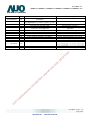
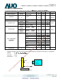
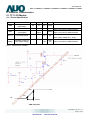
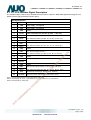
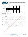
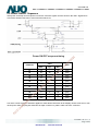
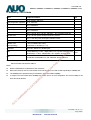
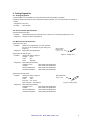
6.6 Power ON/OFF Sequence
VDD power and lamp on/off sequence is as below. Interface signals are also shown in the chart. Signals from
any system shall be Hi-Z state or low level when VDD is off.
30
40
O
10
-
10
0
U
T6
lF
or
T10
AT
AM
T9
100
D
T8
10
O
D
T7
nl
[ms]
[ms]
-
[ms]
-
[ms]
-
[ms]
-
-
[ms]
-
-
[ms]
-
0
16
1000
-
-
Units
-
-
50
10
-
[ms]
[ms]
[ms]
[ms]
tia
T11
-
10
50
rn
a
T5
T4
-
te
175
In
T3
-
se
0.5
T2
01
Max.
/2
Typ.
y
Min.
L
T1
Value
lU
Parameter
2/
10
/2
4
Power ON/OFF sequence timing
fid
en
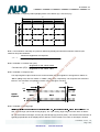
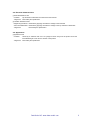
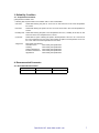
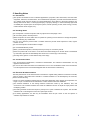
The above on/off sequence should be applied to avoid abnormal function in the display. Please make sure to turn
AU
O
C
on
off the power when you plug the cable into the input connector or pull the cable out of the connector.
G121SN01 V4 rev. 1.4
Page 18/24
Data Modul AG - www.data-modul.com