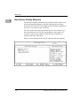
1
CompactPCI® CPV5350 Single Board
Computer and Transition Module
BIOS and Programmer’s
Reference Guide
CPV5350A/PG2
August 27, 2001 Edition
© Copyright 2001 Motorola, Inc.
All Rights Reserved.
Printed in the United States of America.
Parts of this manual are reproduced and adapted from the copyrighted Phoenix
Technologies Ltd., PhoenixBIOS 4.0 User’s Manual, used by permission.
Motorola® and the Motorola symbol are registered trademarks of Motorola, Inc.
Phoenix® is a registered trademark and PhoenixBIOS, PhoenixPHLASH and MultiBoot
are common law trademarks of Phoenix Technologies Ltd.
CompactPCI® is a registered trademark of PCI Industrial Computer Manufacturers Group.
Intel® and the Intel logo are registered trademarks of Intel Corporation.
Pentium® is a registered trademark of Intel Corporation.
Windows® and Windows NT® are registered trademarks of Microsoft in the US and other
countries.
OS/2® is a registered trademark of International Business Machines Corporation.
All other names, products, or services mentioned in this document may be trademarks or
registered trademarks of their respective holders.
Safety Summary
The following general safety precautions must be observed during all phases of operation, service, and repair of this
equipment. Failure to comply with these precautions or with specific warnings elsewhere in this manual could result
in personal injury or damage to the equipment.
The safety precautions listed below represent warnings of certain dangers of which Motorola is aware. You, as the
user of the product, should follow these warnings and all other safety precautions necessary for the safe operation of
the equipment in your operating environment.
Ground the Instrument.
To minimize shock hazard, the equipment chassis and enclosure must be connected to an electrical ground. If the
equipment is supplied with a three-conductor AC power cable, the power cable must be plugged into an approved
three-contact electrical outlet, with the grounding wire (green/yellow) reliably connected to an electrical ground
(safety ground) at the power outlet. The power jack and mating plug of the power cable meet International
Electrotechnical Commission (IEC) safety standards and local electrical regulatory codes.
Do Not Operate in an Explosive Atmosphere.
Do not operate the equipment in any explosive atmosphere such as in the presence of flammable gases or fumes.
Operation of any electrical equipment in such an environment could result in an explosion and cause injury or damage.
Keep Away From Live Circuits Inside the Equipment.
Operating personnel must not remove equipment covers. Only Factory Authorized Service Personnel or other
qualified service personnel may remove equipment covers for internal subassembly or component replacement or any
internal adjustment. Service personnel should not replace components with power cable connected. Under certain
conditions, dangerous voltages may exist even with the power cable removed. To avoid injuries, such personnel
should always disconnect power and discharge circuits before touching components.
Use Caution When Exposing or Handling a CRT.
Breakage of a Cathode-Ray Tube (CRT) causes a high-velocity scattering of glass fragments (implosion). To prevent
CRT implosion, do not handle the CRT and avoid rough handling or jarring of the equipment. Handling of a CRT
should be done only by qualified service personnel using approved safety mask and gloves.
Do Not Substitute Parts or Modify Equipment.
Do not install substitute parts or perform any unauthorized modification of the equipment. Contact your local
Motorola representative for service and repair to ensure that all safety features are maintained.
Observe Warnings in Manual.
Warnings, such as the example below, precede potentially dangerous procedures throughout this manual. Instructions
contained in the warnings must be followed. You should also employ all other safety precautions which you deem
necessary for the operation of the equipment in your operating environment.
Warning
To prevent serious injury or death from dangerous voltages, use extreme
caution when handling, testing, and adjusting this equipment and its
components.
Flammability
All Motorola PWBs (printed wiring boards) are manufactured with a flammability rating
of 94V-0 by UL-recognized manufacturers.
EMI Caution
!
Caution
This equipment generates, uses and can radiate electromagnetic energy. It
may cause or be susceptible to electromagnetic interference (EMI) if not
installed and used with adequate EMI protection.
Lithium Battery Caution
This product contains a lithium battery to power the clock and calendar circuitry.
!
Caution
!
Attention
!
Vorsicht
Danger of explosion if battery is replaced incorrectly. Replace battery only
with the same or equivalent type recommended by the equipment
manufacturer. Dispose of used batteries according to the manufacturer’s
instructions.
Il y a danger d’explosion s’il y a remplacement incorrect de la batterie.
Remplacer uniquement avec une batterie du même type ou d’un type
équivalent recommandé par le constructeur. Mettre au rebut les batteries
usagées conformément aux instructions du fabricant.
Explosionsgefahr bei unsachgemäßem Austausch der Batterie. Ersatz nur
durch denselben oder einen vom Hersteller empfohlenen Typ. Entsorgung
gebrauchter Batterien nach Angaben des Herstellers.
Notice
While reasonable efforts have been made to assure the accuracy of this document,
Motorola, Inc. assumes no liability resulting from any omissions in this document, or from
the use of the information obtained therein. Motorola reserves the right to revise this
document and to make changes from time to time in the content hereof without obligation
of Motorola to notify any person of such revision or changes.
Electronic versions of this material may be read online, downloaded for personal use, or
referenced in another document as a URL to the Motorola Computer Group website. The
text itself may not be published commercially in print or electronic form, edited, translated,
or otherwise altered without the permission of Motorola, Inc.
It is possible that this publication may contain reference to or information about Motorola
products (machines and programs), programming, or services that are not available in your
country. Such references or information must not be construed to mean that Motorola
intends to announce such Motorola products, programming, or services in your country.
Limited and Restricted Rights Legend
If the documentation contained herein is supplied, directly or indirectly, to the U.S.
Government, the following notice shall apply unless otherwise agreed to in writing by
Motorola, Inc.
Use, duplication, or disclosure by the Government is subject to restrictions as set forth in
subparagraph (b)(3) of the Rights in Technical Data clause at DFARS 252.227-7013 (Nov.
1995) and of the Rights in Noncommercial Computer Software and Documentation clause
at DFARS 252.227-7014 (Jun. 1995).
Motorola, Inc.
Computer Group
2900 South Diablo Way
Tempe, Arizona 85282
Table of Contents
CHAPTER 1
PhoenixBIOS Overview
What is a ROM BIOS? ..............................................................................................1-1
ROM BIOS Functions ........................................................................................1-2
Power-On Self Test ....................................................................................................1-3
PhoenixBIOS POST Function Keys ..........................................................................1-5
Phoenix MultiBoot.....................................................................................................1-5
CHAPTER 2
BIOS Setup
Using the Phoenix Setup Program .............................................................................2-1
Starting Setup......................................................................................................2-1
The Setup Interface......................................................................................2-2
The Menu Bar .....................................................................................................2-3
The Legend Bar ...........................................................................................2-3
The Field Help Window ..............................................................................2-4
The General Help Window..........................................................................2-5
Main Menu Selections ...............................................................................................2-6
Memory Menu ...........................................................................................................2-7
The Advanced Menu................................................................................................2-10
Resetting Extended System Configuration Data ..............................................2-12
Floppy Configuration Submenu........................................................................2-12
Floppy Configuration Submenu Options...................................................2-13
IDE Configuration Submenu ............................................................................2-14
IDE Configuration Submenu Options .......................................................2-15
Masters and Slaves ....................................................................................2-16
Primary/Secondary Master/Slave Submenus.............................................2-16
Primary/Secondary Master/Slave Submenu Options ................................2-18
I/O Device Configuration Submenu .................................................................2-19
I/O Device Configuration Submenu Options ............................................2-20
PCI Configuration Submenu.............................................................................2-24
PCI Configuration Submenu Options........................................................2-25
HA Configuration Submenu .............................................................................2-26
HA Configuration Submenu Options ........................................................2-27
PCI/PNP IRQ Configuration Submenu ............................................................2-29
PCI/PNP IRQ Configuration Submenu Options .......................................2-30
Remote Console Submenu................................................................................2-31
vii
The Remote Console Feature .................................................................... 2-31
Remote Console Submenu Options .......................................................... 2-32
Screen Lines .............................................................................................. 2-33
Active After POST .................................................................................... 2-34
Embedded Flash Submenu ............................................................................... 2-34
Embedded Flash Submenu Options .......................................................... 2-35
Security Menu.......................................................................................................... 2-38
Security Menu Options ............................................................................. 2-38
User and Supervisor Passwords ................................................................ 2-40
Status Menu ............................................................................................................. 2-41
Status Menu Options ........................................................................................ 2-42
Boot Menu ............................................................................................................... 2-42
Boot Menu Options .......................................................................................... 2-43
Boot Device Priority Submenu......................................................................... 2-44
Using the Boot Device Priority Submenu ................................................. 2-45
Network Boot ............................................................................................ 2-46
Exit Menu ................................................................................................................ 2-46
Exit Menu Options ........................................................................................... 2-47
CHAPTER 3
Phoenix BIOS Messages
PhoenixBIOS Messages ............................................................................................ 3-1
CHAPTER 4
Power-On Self Tests
Recoverable Power On Self-Test Errors.................................................................... 4-1
POST Terminal Errors ............................................................................................... 4-2
Test Points and Beep Codes....................................................................................... 4-2
CHAPTER 5
Programming Information
Peripheral Component Interconnect (PCI) Local Bus ............................................... 5-1
Watchdog Timer ........................................................................................................ 5-2
Watchdog Timer Operation ................................................................................ 5-3
Enabling the timer ....................................................................................... 5-3
I/O Address Map ....................................................................................................... 5-4
Memory Address Mapping ........................................................................................ 5-6
Video Controller ........................................................................................................ 5-6
EIDE Interface ........................................................................................................... 5-7
Floppy Interface......................................................................................................... 5-7
Parallel Port ............................................................................................................... 5-8
viii
Serial Ports .................................................................................................................5-8
USB............................................................................................................................5-8
Keyboard/Mouse Interface.........................................................................................5-9
DMA Channels ..........................................................................................................5-9
Interrupts ..................................................................................................................5-10
Field Programmable Gate Array Registers ..............................................................5-11
Register Descriptions........................................................................................5-15
STAT .........................................................................................................5-17
ECTRL.......................................................................................................5-18
WDCFG.....................................................................................................5-19
INTEN .......................................................................................................5-21
SCIEN........................................................................................................5-23
NMIEN ......................................................................................................5-24
IRQEN .......................................................................................................5-25
ALEN.........................................................................................................5-26
LEN ...........................................................................................................5-28
POS ............................................................................................................5-29
LNACTRL.................................................................................................5-30
LNBCTRL .................................................................................................5-31
NVRAM ....................................................................................................5-32
USBCTRL .................................................................................................5-33
FLBCTRL..................................................................................................5-34
APPENDIX A
Updating the BIOS
Update Files ..............................................................................................................A-1
Phoenix Phlash Utility ..............................................................................................A-2
Installing Phoenix Phlash...................................................................................A-2
Executing Phoenix Phlash .................................................................................A-2
Disabling Memory Managers ............................................................................A-3
DOS 5.0 (or later version) ..........................................................................A-3
Creating a Boot Diskette.............................................................................A-4
Embedded Flash.................................................................................................A-4
Executing Embedded Flash ........................................................................A-5
Updating from Floppy Disk........................................................................A-5
Updating with Remote Console..................................................................A-6
APPENDIX B
Remote Console Escape Keys
Defined Sequences.................................................................................................... B-1
ix
APPENDIX C
Network Boot
Enabling Network Boot ............................................................................................ C-1
Intel Boot Agent ....................................................................................................... C-2
Boot Agent Setup .............................................................................................. C-4
Boot Agent Setup Options ......................................................................... C-5
Cancelling Network Boot .................................................................................. C-6
APPENDIX D
Related Documentation
Motorola Computer Group Documents .................................................................... D-1
x
List of Figures
Figure 2-1. The basic setup screen.............................................................................2-2
Figure 5-1. Field Programmable Gate Array Watchdog Block Diagram ..................5-3
Figure 5-2. Block diagram for the Field Programmable Gate Array .......................5-12
xi
xii
List of Tables
Table 1-1. PhoenixBIOS functions ............................................................................1-2
Table 1-2. PhoenixBIOS keys....................................................................................1-5
Table 2-1. PhoenixBIOS Main Menu Bar..................................................................2-3
Table 2-2. Legend Bar................................................................................................2-3
Table 2-3. Scroll bar selections ..................................................................................2-6
Table 2-4. Main Menu Selections ..............................................................................2-7
Table 2-5. Memory Menu Selections.........................................................................2-8
Table 2-6. Advanced Menu Selections ....................................................................2-11
Table 2-7. Floppy Configuration Submenu Selections ............................................2-13
Table 2-8. IDE Configuration Submenu Selections.................................................2-15
Table 2-9. Primary/Secondary Master/Slave
Submenu Options................................................................................................2-18
Table 2-10. I/O Device Configuration Submenu Options........................................2-20
Table 2-11. PCI Configuration Submenu Options ...................................................2-25
Table 2-12. HA Configuration Submenu Options ...................................................2-28
Table 2-13. PCI/PNP IRQ Configuration Submenu Options...................................2-30
Table 2-14. Remote Console Submenu Options ......................................................2-32
Table 2-15. Embedded Flash Submenu Options ......................................................2-35
Table 2-16. Security Menu Options .........................................................................2-38
Table 2-17. Status Menu Options.............................................................................2-42
Table 2-18. Boot Menu Options...............................................................................2-43
Table 2-19. Key Functions for the Boot Device Priority Submenu .........................2-46
Table 2-20. Exit Menu Options................................................................................2-47
Table 3-1. PhoenixBIOS Messages............................................................................3-1
Table 4-1. Checkpoint Codes and Beep Codes ..........................................................4-3
Table 5-1. I/O Addresses............................................................................................5-4
Table 5-2. Memory Address.......................................................................................5-6
Table 5-3. On-board Drive Options ...........................................................................5-7
Table 5-4. DMA Channels .........................................................................................5-9
Table 5-5. Interrupt Channels...................................................................................5-10
Table 5-6. FPGA Mapping for I/O Ports..................................................................5-12
Table 5-7. FPGA Register Sets ................................................................................5-12
Table 5-8. FPGA Registers ......................................................................................5-14
Table 5-9. Index and Data Register Address and Function......................................5-15
xiii
Table 5-10. Map of the FPGA Register Set............................................................. 5-16
Table 5-11. Bit Descriptions for the STAT Register ................................................ 5-17
Table 5-12. Bit Descriptions for the ECTRL Register ............................................ 5-18
Table 5-13. Bit Descriptions for the WDCFG Register........................................... 5-19
Table 5-14. Bit Values for Selecting Watchdog Timeout Time ............................... 5-19
Table 5-15. Bit Values Defining Watchdog Timeout and Disabling ....................... 5-20
Table 5-16. Bit Descriptions for the INTUM Register ............................................ 5-21
Table 5-17. IRQ Line Bit Values ............................................................................. 5-21
Table 5-18. Bit Descriptions for the SCIEN Register ............................................. 5-23
Table 5-19. Bit Descriptions for the NMIEN Register ............................................ 5-24
Table 5-20. Bit Descriptions for the IRQEN Register............................................. 5-25
Table 5-21. Bit Descriptions for the ALEN Register .............................................. 5-26
Table 5-22. Bit Descriptions for the LEN Register ................................................. 5-28
Table 5-23. Bit Descriptions for the POS Register.................................................. 5-29
Table 5-24. Bit Descriptions for the LNACTRL Register....................................... 5-30
Table 5-25. Bit Descriptions for the LAN B Register ............................................. 5-31
Table 5-26. Bit Descriptions for the NVRAM Register .......................................... 5-32
Table 5-27. Bit Selections for the 32K NVRAM Memory Bank ............................ 5-32
Table 5-28. Bit Descriptions for the USBCTRL Register ....................................... 5-33
Table 5-29. Bit Descriptions for the FLBCTRL Register ....................................... 5-34
Table A-1. Typical BIOS Update ............................................................................ A-1
Table B-1. Remote Console Escape Sequences ...................................................... B-1
Table C-1. Boot Agent Setup Menu Fields ............................................................. C-5
Table D-1. Motorola Computer Group Documents ................................................. D-1
xiv
About This Manual
This CompactPCI CPV5350 Single Board Computer and Transition
Module BIOS and Programmer’s Reference Guide is based on the
CPV5350 BIOS v3.0RM02. It gives you instructions for configuring the
PhoenixBIOS installed on these standard models of the CPV5350 and
CPV5350B Single Board Computer:
Model
Numbers
Description
CPV5350-266
CompactPCI Single Board Computer with 266 MHz
processor and 64 or 128MB SDRAM
CPV5350-333
CompactPCI Single Board Computer with 333 MHz
processor and 64 or 128MB SDRAM
CPV5350-500
CompactPCI Single Board Computer with 500 MHz
Pentium III processor
It also gives you instructions for using PhoenixBIOS utilities. Use this
guide with the CPV5350 CompactPCI Single Board Computer and
Transition Module Installation Guide (part number CPV5350A/IHx).
Summary of Changes
This section summarizes major changes made to this manual.
Date:
August 22, 2001
Change:
Added section titled Phoenix MultiBoot on page 1-5
Revised Chapter 2, BIOS Setup and associated setup
screens
Revised Chapter 3, Phoenix BIOS Messages
Revised Chapter 4, Power-On Self Tests
Added Appendix A, Updating the BIOS
Added Appendix B, Remote Console Escape Keys
Added Appendix C, Network Boot
Revised Appendix D, Related Documentation
xv
Overview of Contents
This manual is divided into these chapters and appendices:
Chapter 1, PhoenixBIOS Overview, describes the ROM BIOS and ROM
BIOS functions, the power-on self tests (POST), BIOS services, system
hardware requirements, fixed disk drives, function keys and multiboot.
Chapter 2, BIOS Setup, describes the menus and features of the
PhoenixBIOS setup utility. This utility lets you modify BIOS settings and
control the special features of your computer.
Chapter 3, Phoenix BIOS Messages, lists the messages the BIOS can
display.
Chapter 4, Power-On Self Tests, describes a series of programs run by the
PhoenixBIOS.
Chapter 5, Programming Information, gives you information about the
Peripheral Component Interconnect (PCI) bus, watchdog timer, I/O
address map, video controller, EIDE and floppy drive interfaces and the
Field Programmable Gate Array (FPGA) registers.
Appendix A, Updating the BIOS, tells you how to update the BIOS without
installing a new ROM BIOS chip using the Phoenix Phlash Utility or
Embedded Flash.
Appendix B, Remote Console Escape Keys, defines a range of escaped
character sequences to emulate function or navigation keys, or key
combinations.
Appendix C, Network Boot, explains how to configure the BIOS for
network boot and gives you information about the Ethernet boot ROM for
the on-board Ethernet devices.
Appendix D, Related Documentation, lists other Motorola Computer
Group publications that provide additional sources of information related
to the product.
xvi
Comments and Suggestions
Motorola welcomes and appreciates your comments on our
documentation. We want to know what you think about our manuals and
how we can make them better. Mail comments to:
Motorola Computer Group
Reader Comments DW164
2900 S. Diablo Way
Tempe, Arizona 85282
You can also submit comments to the following e-mail address:
[email protected]
In all your correspondence, please list your name, position, and company.
Be sure to include the title and part number of the manual and tell how you
used it. Then tell us your feelings about its strengths and weaknesses and
any recommendations for improvements.
Conventions Used in This Manual
We use the following typographical conventions in this document:
bold
is used for user input that you type just as it appears; it is also used for
commands, options and arguments to commands, and names of
programs, directories and files.
italic
is used for names of variables to which you assign values. Italic is also
used for comments in screen displays and examples, and to introduce
new terms.
courier
is used for system output (for example, screen displays, reports),
examples, and system prompts.
<Enter>, <Return> or <CR>
xvii
<CR> represents the carriage return or Enter key.
CTRL
represents the Control key. Execute control characters by pressing the
Ctrl key and the letter simultaneously, for example, Ctrl-d.
xviii
1PhoenixBIOS Overview
1
This chapter gives you a brief introduction and overview of the
PhoenixBIOS software. It covers:
❏
a description of the ROM BIOS including ROM BIOS functions
❏
the power-on self tests (POST)
❏
BIOS services
❏
system hardware requirements
❏
fixed disk drives
❏
function keys
❏
multiboot
What is a ROM BIOS?
A ROM BIOS (Basic Input/Output System) is a set of programs
permanently stored in a ROM (Read-Only Memory) chip located on the
computer motherboard. These programs manage the hardware devices
installed on your computer. When you turn on your computer, the ROM
BIOS initializes and tests these devices. During run-time, the ROM BIOS
provides the operating system and application programs with access to
these devices. You can also use the BIOS Setup program to change your
computer’s hardware or behavior.
Software works best when it operates in layers. The ROM BIOS is the
bottom software layer in the computer. It functions as the interface
between the hardware layer in the computer. It functions as the interface
between the hardware and the other layers of software, isolating them from
the details of how the hardware works. This arrangement lets you change
hardware devices without having to install a new operating system.
1-1
1
PhoenixBIOS Overview
This diagram shows how the ROM BIOS interfaces with the hardware and
other layers of software.
Application Programs
Operating System and
Device Drivers
ROM BIOS
System Hardware
ROM BIOS Functions
The PhoenixBIOS software performs these functions. Refer to Table 1-1
Table 1-1. PhoenixBIOS functions
1-2
Function
Description
Configures Devices
Using the Setup program, you can enable,
configure, and optimize the hardware devices in
your system (clock, memory, disk drives).
Initializes Hardware at Boot
At power-on or reset, the BIOS performs PowerOn-Self Test (POST) routines to test system
resources and run the operating system.
Executes Run-Time Routines
The BIOS gives you access to basic hardware
routines called from DOS and Windows
applications.
Computer Group Literature Center Web Site
Power-On Self Test
Power-On Self Test
The ROM BIOS initializes and configures the computer hardware when
you turn on your computer (system boot). It runs a series of complex
programs called the Power-On Self Test (POST), which performs a
number of tasks, including:
❏
Test Random Access Memory (RAM)
❏
Conduct an inventory of the hardware devices installed in the
computer
❏
Configure hard and floppy disks, keyboard, monitor, and serial and
parallel ports
❏
Configure other devices installed in the computer such as CD-ROM
drives and sound cards
❏
Initialize computer hardware required for computer features such as
plug and play and power management
❏
Run Setup if requested
❏
Load and run the Operating System (OS) such as DOS, OS/2,
UNIX, or Windows NT
BIOS Services
The second task of the ROM BIOS is to give the operating system, device
drivers, and application programs access to the system hardware. It
performs this task with a set of program routines, called BIOS Services,
which are loaded into high memory at boot time.
The number of BIOS Services is always changing. The BIOS Services of
PhoenixBIOS provide precise control of hardware devices such as disk
drives, which require careful management and exhaustive checking for
errors. They also help manage new computer features such as power
management, plug and play, and MultiBoot.
http://www.motorola.com/computer/literature
1-3
1
1
PhoenixBIOS Overview
System Hardware Requirements
PhoenixBIOS requires these hardware components on the motherboard:
❏
CPU (486 or later)
❏
AT-compatible and MC146818 RTC-compatible chipset
❏
AT or PS/2-compatible Keyboard controller
❏
At least 1 MB of system RAM
❏
The power-on self test (POST) of the BIOS initializes additional
ROM BIOS extensions (Option ROMs) if they are accessible in the
proper format. These special requirements apply to such adapter
ROMs. The:
– code must reside in the address space between C0000H and
F0000H.
– code must reside on a 2K boundary.
– first two bytes of the code must be 55H and AAH.
– third byte must contain the number of 512-byte blocks.
– fourth byte must contain a jump to the start of the initialization
code.
– code must checksum to zero (byte sum).
Note
The address space from C0000h to C8000h is reserved for
external video adapters (for example; EGA, VGA). Part of the
address space from D0000h to E0000h is typically used by
expanded memory (EMS).
Fixed Disk Drives
PhoenixBIOS supports up to four fixed-disk drives. You can modify the
user-defined drive type for each fixed disk listed in Setup by using the
menus of the Setup program. This feature avoids the need for customized
software for non-standard drives.
1-4
Computer Group Literature Center Web Site
PhoenixBIOS POST Function Keys
PhoenixBIOS POST Function Keys
PhoenixBIOS uses these keys during POST (Table 1-2):
Table 1-2. PhoenixBIOS keys
Press:
To:
<F2>
Enter the Setup program during POST
<Esc>
Launch the Boot First menu
<Space>
Abort the extended memory test
Phoenix MultiBoot
Phoenix MultiBoot expands your boot options by letting you choose your
boot device. You can specify your boot device in Setup, or you can choose
a different device each time you boot by selecting a boot device from the
Boot First menu.
When you press <Esc> during POST, the BIOS displays a menu similar to
this instead of launching the operating system:
This “Boot First” menu displays the boot sequence specified in the Setup
Utility’s Boot menu and lets you:
❏
Override the existing boot sequence (for this boot only) by selecting
another boot device. If the specified device does not load the
operating system, the BIOS reverts to the previous boot sequence
❏
Enter Setup
http://www.motorola.com/computer/literature
1-5
1
1
PhoenixBIOS Overview
❏
Press <Esc> to continue with the existing boot sequence
To specify a different boot device or enter Setup:
1. use the up and down arrow keys to select an option
2. press <Enter>
3. press <Esc> to cancel and continue with the existing boot sequence
The Boot First menu is configured in the Boot menu of the Setup Utility.
For information refer to Boot Menu on page 2-42.
1-6
Computer Group Literature Center Web Site
2BIOS Setup
2
Using the Phoenix Setup Program
This chapter describes the PhoenixBIOS Setup program (BIOS Setup
Utility). With this utility, you can modify BIOS settings and control the
special features of your computer. The Setup program uses various menus
for making changes and turning features on or off.
Note
The menus shown in this chapter are those in effect when the
manual was printed. The actual menus displayed on your screen
may be different and depend in part on the features, hardware,
and version of the BIOS installed on your computer.
Starting Setup
The PhoenixBIOS setup utility starts when you turn on or reboot the
computer. It checks and configures the system through a power-on self test
(POST). During POST, the following message appears at the bottom of the
screen:
Press <F2> to enter SETUP
To start the PhoenixBIOS setup utility, press <F2>.
The BIOS Setup Utility starts and displays the Main Menu.
Note
If POST finishes before you respond and you still want to enter
Setup, restart the computer and try again.
2-1
BIOS Setup
2
The Setup Interface
The Setup program uses a menu-driven interface. Each Setup screen has a
menu bar, a legend bar, and a field-specific help window as shown in
Figure 2-1. An options window is also available for each field with
predefined values.
Figure 2-1. The basic setup screen
See Table 2-1 for a description of the fields on this menu.
2-2
Computer Group Literature Center Web Site
Using the Phoenix Setup Program
The Menu Bar
2
The Menu Bar at the top of the window lists these selections. Refer to
Table 2-1.
Table 2-1. PhoenixBIOS Main Menu Bar
Use this menu
bar selection:
To:
Main
set time and view basic system configuration
Memory
view and configure system memory and cache
Advanced
set up drives and configure I/O and chipset features
Security
set passwords and access options
Status
view temperature and power supply status
Boot
specify boot options
Exit
exit the Setup Utility with or without saving
changes
Use the left/right arrow keys to make a selection.
See the section below, “exiting setup”, for information about exiting the
main menu.
The Legend Bar
Use the keys listed in the legend bar on the bottom to make your selections
or exit the current menu. Table 2-2 describes the legend keys and their
alternates.
Table 2-2. Legend Bar
Use this key:
To:
<F1> or <Alt-H>
get general help
<Esc>
exit this menu
← or → arrow keys
select a different menu
↑ or ↓ arrow keys
move the cursor up and down
<Tab> or <Shift-Tab>
cycle the cursor up and down
http://www.motorola.com/computer/literature
2-3
BIOS Setup
Table 2-2. Legend Bar (Continued)
2
Use this key:
To:
<Home> or <End>
move the cursor to the top or bottom of the
window
<PgUp> or <PgDn>
move the cursor to the next or previous
page
<F5> or <->
select the previous value for the field
<F6> or <+> or <Space>
select the next value for the field
<F9>
load the default configuration values for
all menus
<F10>
save and exit
<Enter>
execute a command or select > a submenu
To select an item, use the arrow keys to move the cursor to the field you
want. Then use the plus and minus value keys to select a value for that
field. The Save Value commands in the Exit Menu save the values
currently displayed in all the menus.
To display a submenu, use the arrow keys to move the cursor to the
submenu you want. Then press <Enter>. A pointer marks all submenus.
The Field Help Window
The help window on the right side of each menu displays the help text for
the currently selected field. It updates as you move the cursor to each field.
2-4
Computer Group Literature Center Web Site
Using the Phoenix Setup Program
The General Help Window
2
Pressing <F1> or <Alt-H> on any menu brings up the General Help
window that describes the legend keys and their alternates:
General Help
Setup changes system behavior by modifying the BIOS
configuration parameters. Selecting incorrect values
may cause system boot failure; load Setup Default values
to recover.
<Up/Down> arrows select fields in current menu.
<PgUp/PgDn> moves to previous/next page on scrollable menus.
<Home/End> moves to top/bottom item of current menu.
Within a field, <F5> or <-> selects next lower value and
<F6>, <+>, or <Space> selects next higher value.
<Left/Right> arrows select menus on menu bar.
<Enter> displays more options for items marked with a P.
<Enter> also displays an option list on some fields.
<F9> loads factory-installed Setup Default values.
<F10> restores previous values from CMOS.
<ESC> or <Alt-X> exits Setup; in sub-menus, pressing these
keys returns to the previous menu.
<F1> or <Alt-H> displays General Help (this screen).
_
[Continue]
http://www.motorola.com/computer/literature
2-5
BIOS Setup
The scroll bar on the right of any window indicates that there is more than
one page of information in the window. Refer to Table 2-3.
2
Table 2-3. Scroll bar selections
Use:
To:
<PgUp> and <PgDn>
display all the pages
<Home> and <End>
display the first and last
page
<Enter>
display each page and
then exit the window
<Esc>
to exit the current
window
Main Menu Selections
This screen appears when you select the Main Menu.
2-6
Computer Group Literature Center Web Site
Memory Menu
You can make the following selections on the Main Menu itself. Refer to
Table 2-4. Use the submenus for other selections.
Table 2-4. Main Menu Selections
Feature
Default
Options
Description
BIOS Version
N/A
information only
Displays the BIOS version on the
CPU board
Board Serial No.
N/A
information only
Displays the serial number of the
CPU board
CPU Type
N/A
information only
Displays the type of processor
detected during bootup
CPU Speed
N/A
information only
Displays the processor speed
detected during bootup
Host Bus
Frequency
N/A
information only
Displays the front side bus
frequency, either 66MHz or
100MHz
Cache Ram
N/A
information only
Displays the amount of level 2
cache detected during bootup
Total Memory
N/A
information only
Displays the total memory
detected during bootup
System Time
00:00:00
HH:MM:SS
Sets the system time
System Date
01/01/2000
MM/DD/YY
Sets the system date
Memory Menu
The Memory Menu lets you view and customize memory and cache
settings.
http://www.motorola.com/computer/literature
2-7
2
BIOS Setup
This screen appears when you select the Memory Menu:
2
Table 2-5 describes the selections available in the Memory Menu.
Table 2-5. Memory Menu Selections
Feature
Default
Options
Description
Cache RAM
N/A
information only
Displays the amount of L2 cache
detected during bootup
Total Memory
N/A
information only
Displays the total memory
detected during bootup
Memory Bank 0
N/A
information only
Displays the amount of memory
detected in this DIMM socket
L2 Cache
Enabled
Enabled
Disabled
Enable or disable the L2 cache
L2 Cache ECC
Support (hidden if
L2 Cache is
Disabled)
Enabled
Enabled
Disabled
Enable or disable L2 cache ECC
support. Disabling support
increases CPU performance
slightly at the expense of error
correction
2-8
Computer Group Literature Center Web Site
Memory Menu
Table 2-5. Memory Menu Selections (Continued)
2
Feature
Default
Options
Description
ECC Memory
Config
Disabled
Disabled
Disables memory error checking
EC
Enables memory error checking
only
ECC
Enables memory error checking
and correction
ECC Scrub
Enables memory error checking
and correction with hardware
scrubbing
None
Disables assertion of SERR# on
memory error
Single Bit
Enables SERR# assertion on
single-bit memory errors
Multiple Bit
Enables SERR# assertion on
multi-bit memory errors
Both
Enables SERR# assertion on both
single and multi-bit memory
errors
SERR Signal
Condition (hidden
if ECC Memory
Config is
Disabled)
Multiple Bit
http://www.motorola.com/computer/literature
2-9
BIOS Setup
2
The Advanced Menu
The Advanced menu lets you set up drives and configure I/O and advanced
chipset features. Select “Advanced” from the menu bar on the Main Menu
to display this menu:
!
Caution
2-10
Setting items on the Advanced Menu and its submenus to incorrect values
may cause your system to malfunction. Make sure you alter only settings
you thoroughly understand.
Computer Group Literature Center Web Site
The Advanced Menu
Table 2-6 describes the selections available on the Advanced Menu.
2
Table 2-6. Advanced Menu Selections
Feature
Default
Options
Description
Plug and Play OS
No
No
Yes
Yes lets the plug-and-play (PnP)
operating system configure PnP
devices not required for boot. No
makes the BIOS configure them.
Reset
Configuration
Data
No
No
Yes
Yes clears the Extended System
Configuration Data (ESCD) area.
Legacy USB
Support
Enabled
Disabled
Enabled
Enabling legacy USB lets you
use a USB keyboard as a PS/2
keyboard with a non-USB aware
operating system. It also enables
USB boot support from a USB
floppy.
http://www.motorola.com/computer/literature
2-11
BIOS Setup
2
Resetting Extended System Configuration Data
The Extended System Configuration Data (ESCD) area stores information
about the devices in your system. In most cases, when you add or remove
devices, the BIOS automatically updates the ESCD based on the
configuration detected during POST. However, if you want to clear the
ESCD, you can use the Reset Configuration Data feature in the Advanced
menu.
Setting the Reset Configuration Data feature to "Yes" clears the ESCD
after you exit Setup. At the next boot, the ESCD updates and Reset
Configuration Data automatically returns to “No”.
Floppy Configuration Submenu
The Floppy Configuration submenu lets you set up any floppy drives in
your system. When you enter the Floppy Configuration submenu, this
screen appears:
2-12
Computer Group Literature Center Web Site
The Advanced Menu
Floppy Configuration Submenu Options
2
Table 2-7 describes the selections available in the Floppy Configuration
submenu.
Table 2-7. Floppy Configuration Submenu Selections
Feature
Default
Options
Description
Floppy Controller
Enabled
Disabled
Disables the on-board floppy
disk controller
Enabled
Enables the floppy disk
controller and allows the user to
specify the base address
Auto
BIOS selects the floppy disk
controller configuration
OS Controlled
Allows a plug-n-play operating
system to configure the floppy
disk controller
Base I/O Address
(displayed if
Floppy Controller
is Enabled
Primary
Primary
Secondary
Specifies the base I/O address for
the enabled floppy disk controller
Diskette A
1.44 MB, 3 1/2
inch
Disabled
360 KB, 5 1/4 inch
1.2 MB, 5 1/4 inch
720 KB, 3 1/2 inch
1.44 MB, 3 1/2 inch
2.88 MB, 3 1/2 inch
Specifies the type of floppy disk
drive installed in your system
Diskette B
Disabled
Disabled
360 KB, 5 1/4 inch
1.2 MB, 5 1/4 inch
720 KB, 3 1/2 inch
1.44 MB, 3 1/2 inch
Specifies the type of floppy disk
drive installed in your system
Floppy Check
Disabled
Enabled
Disabled
Enabled verifies the floppy drive
type on boot.
Disabled speeds boot
http://www.motorola.com/computer/literature
2-13
BIOS Setup
2
IDE Configuration Submenu
The IDE Configuration submenu lets you set up any IDE drives in your
system. When you enter the IDE Configuration submenu, this screen
appears:
2-14
Computer Group Literature Center Web Site
The Advanced Menu
IDE Configuration Submenu Options
2
Table 2-8 describes the selections available in the IDE Configuration
submenu.
Table 2-8. IDE Configuration Submenu Selections
Feature
Default
Options
Description
Local Bus IDE
Adapter
Both
Disabled
Primary
Secondary
Both
Selects which channels of the
onboard IDE controller are
enabled
Large Disk Access
Mode
DOS
DOS
Other
Select DOS for most operating
systems, including DOS,
Windows, and Novell NetWare.
For other operating systems,
select Other. If installing a new
OS and the drive fails, change
this setting and try again.
Different operating systems
require different representations
of drive geometries
SMART Device
Monitoring
Disabled
Disabled
Enabled
Enable or Disable SelfMonitoring Analysis-Reporting
Technology (SMART) which
monitors and warns of an
imminent failure on a hard-disk
drive
http://www.motorola.com/computer/literature
2-15
BIOS Setup
2
Masters and Slaves
The Master and Slave settings on the IDE Configuration submenu control
these types of drive devices:
❏
hard disk
❏
removable disk
❏
CD-ROM
PhoenixBIOS supports up to two IDE disk controllers, called primary and
secondary controllers. Each controller supports one master drive and one
optional slave drive. There is one IDE connector for each controller on
your system, usually labeled “Primary IDE” and “Secondary IDE”.
When you enter the IDE Configuration submenu, it displays the results of
Autotyping. Autotyping is information each drive provides about its own
size and other characteristics and their arrangement as masters or slaves on
your machine.
Note
Do not change these settings unless your installed drive does not
autotype properly (for example; an older hard disk drive that does
not support autotyping).
If you need to change your drive settings, use one of the Master
or Slave submenus.
Primary/Secondary Master/Slave Submenus
The Primary/Secondary Master/Slave submenus let you configure your
system for the drives installed.
2-16
Computer Group Literature Center Web Site
The Advanced Menu
When you enter one of the Primary/Secondary Master/Slave submenus, a
screen appears:
When type is set to Auto, the detected device is noted in the screen heading
and its characteristics display. Use the plus or minus keys or the space bar
to specify a different Type.
http://www.motorola.com/computer/literature
2-17
2
BIOS Setup
2
Primary/Secondary Master/Slave Submenu Options
Table 2-9 describes the selections available in the Primary/Secondary
Master/Slave submenus.
Table 2-9. Primary/Secondary Master/Slave
Submenu Options
Feature
Default
Options
Description
Type
Auto
Auto
Autotypes installed drives and
displays the drive characteristics
None
Manually specifies that no drive
is installed
CD-ROM
Specifies a CD-ROM drive
IDE Removable
Specifies an IDE removable
storage device (a Flash disk, for
example)
ATAPI Removable
Specifies an ATAPI removable
storage device (for example; a
Zip drive)
User
Lets you manually configure the
system for the installed drive
Cylinders
(selectable when
Type=User)
N/A
0 to 65535
Specifies the number of drive
cylinders
Heads (selectable
when Type=User)
N/A
1 to 16
Specifies the number of drive
heads
Sectors (selectable
when Type=User)
N/A
0 to 63
Specifies the number of sectors
per track
Maximum
Capacity
N/A
information only
Displays the calculated drive
capacity based on the maximum
number of addressable sectors
Multi- Sector
Transfers
(selectable when
Type=User)
N/A
Disabled 2, 4, 8, or
16 sectors
Specifies the number of sectors
per block for multiple-sector
transfers
2-18
Computer Group Literature Center Web Site
The Advanced Menu
Table 2-9. Primary/Secondary Master/Slave
Submenu Options (Continued)
Feature
Default
Options
Description
LBA Mode
Control (selectable
when Type=User)
N/A
Enabled
Disabled
Enabling LBA causes logical
block addressing to be used in
place of cylinders, heads, and
sectors
32 Bit I/O
Disabled
Enabled
Disabled
Enables or disables 32-bit data
transfers between the CPU and
the IDE controller
SMART
Monitoring
N/A
information only
Displays whether or not SMART
monitoring is enabled for the
drive
Transfer Mode
(selectable when
Type=User)
N/A
Standard
Fast PIO 1, 2, 3, or 4
FPIO 3 / DMA 1
FPIO 4 / DMA 2
Specifies the method for moving
data to and from the drive
(autotype for the optimum
transfer mode)
Ultra DMA Mode
(selectable when
Type=User)
N/A
Disabled
Mode 0, 1, 2, 3, or 4
Specifies the Ultra DMA mode
used for moving data to and from
the drive (Modes 3 and 4 are not
supported on the CPV5350)
2
I/O Device Configuration Submenu
Most devices in the computer require the exclusive use of system resources
for operation. These system resources can include Input and Output (I/O)
port addresses and interrupt lines.
The I/O Device Configuration submenu lets you specify addresses,
interrupts, and operating mode settings for your system’s I/O devices.
http://www.motorola.com/computer/literature
2-19
BIOS Setup
When you enter the I/O Device Configuration submenu, this screen
appears:
2
I/O Device Configuration Submenu Options
Table 2-10 describes the selections available in the I/O Device
Configuration submenu.
Table 2-10. I/O Device Configuration Submenu Options
Feature
Default
Options
Description
PS/2 Mouse
Auto Detect
Disabled
Disables the mouse port and frees
up IRQ 12
Enabled
Enables the mouse port even if
no mouse is present
Auto Detect
Enables mouse port only if
mouse is present
OS Controlled
Allows plug and play operating
system to configure the port after
POST
2-20
Computer Group Literature Center Web Site
The Advanced Menu
Table 2-10. I/O Device Configuration Submenu Options (Continued)
Feature
Serial Port A
1
2
Default
Options
Description
Enabled
Disabled
Disables the port
Enabled
Enables the port and lets you
specify the base address and
interrupt
Auto
Enables mouse port only if
mouse is present
OS Controlled
Lets a plug and play operating
system to configure the port after
POST
Base I/O Address
(Serial Port A;
displays only
when Port A is
Enabled and not in
use by Remote
Console)
3F8
3F8
2F8
3E8
2E8
Specifies the base I/O address for
the port
Interrupt
(Serial Port A;
displays only
when Port A is
Enabled and not in
use by Remote
Console)
IRQ4
IRQ3
IRQ4
Specifies the interrupt assigned
to the port 2
Serial Port B 1
Enabled
Disabled
Disables the port
Enabled
Enables the port and lets you
specify the base address and
interrupt
Auto
Enables mouse port only if
mouse is present
OS Controlled
Lets a plug-n-play operating
system configure the port after
POST
1
If the Remote Console is using Serial Ports A or B, the port settings are configured using the
Remote Console submenu.
http://www.motorola.com/computer/literature
2-21
BIOS Setup
Table 2-10. I/O Device Configuration Submenu Options (Continued)
2
Feature
Default
Options
Description
Base I/O Address
(Serial Port B;
displays only
when Port B is
Enabled and not in
use by Remote
Console)
2F8
3F8
2F8
3E8
2E8
Specifies the base I/O address for
the port
Interrupt (Serial
Port B; displays
only when Port B
is Enabled and not
in use by Remote
Console)
IRQ3
IRQ3
IRQ4
Specifies the interrupt assigned
to the port 2
Parallel Port
Enabled
Disabled
Disables the port
Enabled
Enables the port and lets you
specify base address, interrupt,
and DMA channel
Auto
BIOS selects configuration
OS Controlled
Lets a plug and play operating
system configure the port after
POST
Output only
Bi-directional
EPP
ECP
Specifies the transmission mode
for the parallel port
Mode (Parallel
Port; hidden if
Parallel Port is
Disabled
2-22
Bi-directional
Computer Group Literature Center Web Site
The Advanced Menu
Table 2-10. I/O Device Configuration Submenu Options (Continued)
2
Feature
Default
Options
Description
Base I/O Address
(Parallel Port;
displays only
when Parallel Port
is Enabled
378
378
278
3BC
Specifies the base I/O address for
the parallel port
Interrupt (Parallel
Port; displays only
when Parallel Port
is Enabled)
IRQ7
IRQ5
IRQ7
Specifies the interrupt assigned
to the port 2
DMA Channel
(Displays only
when Parallel Port
is Enabled and
Mode=ECP)
DMA3
DMA1
DMA3
Specifies the DMA channel
assigned to the parallel port
2
If you choose the same I/O address or interrupt for more than one device, the menu displays an
asterisk (*) by the conflicting settings. It also displays this message at the bottom of the menu.
You may have to page down to see this message:
* Indicates a DMA, Interrupt, I/O, or memory
resource conflict with another device.
Resolve the conflict by selecting other settings for the devices.
http://www.motorola.com/computer/literature
2-23
BIOS Setup
2
PCI Configuration Submenu
The PCI Configuration submenu lets you setup PCI devices in your
system. When you enter the PCI Configuration submenu, you see this
screen:
2-24
Computer Group Literature Center Web Site
The Advanced Menu
PCI Configuration Submenu Options
2
Table 2-11 describes the selections available in the PCI Configuration
submenu.
Table 2-11. PCI Configuration Submenu Options
Feature
Default
Options
Description
Default Primary
Video Adapter
AGP
AGP
PCI
Specifies the default display
device when multiple video
adapters are installed
On-Card Ethernet 1
Enabled
Enabled
Enables the Ethernet controller
and lets the BIOS or operating
system configure and use it
Disabled
Disables the device and makes it
inaccessible by the BIOS or
operating system 1
Front
Front connects the Ethernet
signals to the front panel of the
CPU board
Rear
Rear connects the Ethernet
signals to the connector on the
rear transition module (if used)
Ethernet 1
Connection
Front
Ethernet 1 Option
ROM
Disabled
Enabled
Disabled
Enable or disable the execution
of the expansion ROM for the
on-board Ethernet controller 2
On-Card Ethernet 2
Enabled
Enabled
Enables the Ethernet controller
and lets the BIOS or operating
system configure and use it
Disabled
Disables the device so it is not
accessible by the BIOS or
operating system 1
Front
Front connects the Ethernet
signals to the front panel of the
CPU board
Rear
Rear connects the Ethernet
signals to the connector on the
rear transition module (if used)
Ethernet 2
Connection
Front
http://www.motorola.com/computer/literature
2-25
BIOS Setup
Table 2-11. PCI Configuration Submenu Options (Continued)
2
Feature
Default
Options
Description
Ethernet 2 Option
ROM
Disabled
Enabled
Disabled
Enable or disable the execution
of the expansion ROM for the
on-board Ethernet controller 2
USB Connection
Front
Front
Front connects the USB signals
to the front panel of the CPU
board
Rear
Rear connects the USB signals to
the connector on the rear
transition module (if used)
1
You cannot use any Ethernet controller features when it is disabled
If the on-board Ethernet controller option ROM is disabled, you can still use the Ethernet
functions, but you cannot boot through the Ethernet connection or configure Ethernet boot
options. Refer to Appendix C, Network Boot.
2
HA Configuration Submenu
The HA Configuration submenu lets you configure high availability
chassis options.
2-26
Computer Group Literature Center Web Site
The Advanced Menu
When you enter the HA Configuration submenu, this screen appears:
2
HA Configuration Submenu Options
Table 2-12 describes the selections available in the HA Configuration
submenu.
Note
HA Configuration occurs only after the initial power-up. You
must cycle power to this CPU before changes take effect. If a
Domain is already controlled by the other CPU, this processor
does not override and re-configure the Domain.
http://www.motorola.com/computer/literature
2-27
BIOS Setup
2
Table 2-12. HA Configuration Submenu Options
Feature
Default
Options
Description
HA Config
Enabled
Disabled
Disables BIOS configuration of
high availability chassis
Enabled
Enables user selected Domain A
and Domain B configuration of
high availability chassis
Split
Automatically detect, enable, and
power slots for this CPU Domain
Disabled
BIOS does not configure Domain
A
Enabled
Enables Domain A and powers
slots
Disabled
BIOS does not configure Domain
B
Enabled
Enables Domain B and powers
slots
Domain A
(displays only
when HA Config is
Enabled)
Enabled
Domain B (displays
only when HA
Config is Enabled)
Enabled
2-28
Computer Group Literature Center Web Site
The Advanced Menu
PCI/PNP IRQ Configuration Submenu
2
The PCI/PNP IRQ Configuration submenu lets you configure IRQ
resources.
When you enter the PCI/PNP IRQ Configuration submenu, this screen
appears:
http://www.motorola.com/computer/literature
2-29
BIOS Setup
2
PCI/PNP IRQ Configuration Submenu Options
Table 2-13 describes the selections available in the PCI/PNP IRQ
Configuration submenu.
Table 2-13. PCI/PNP IRQ Configuration Submenu Options
Feature
Default
Options
Description
IRQ 9 and IRQ 11
Reserved
Available
Reserved
Specifies whether an IRQ is
available for PCI or PnP devices
or reserved for use by a legacy
ISA device
PCI IRQ Lines 1-4
Auto Select
Disabled
Disables the PCI Interrupt line
(A, B, C, or D)
Auto Select
BIOS selects IRQ
3, 4, 5, 7, 9, 10, 11,
12, 14, 15
Specifies an IRQ to assign to the
PCI line
Note
If you choose an interrupt already in use, the menu displays an asterisk (*) at
the conflicting settings. It also displays this message at the bottom of the
menu. You may have to page down to see this message.
* Indicates a DMA, Interrupt, I/O, or memory resource
conflict with another device.
Resolve the conflict by selecting other settings for the devices.
2-30
Computer Group Literature Center Web Site
The Advanced Menu
Remote Console Submenu
2
The Remote Console submenu lets you configure the BIOS to enable
access from a remote terminal.
When you enter the Remote Console submenu, this screen appears:
The Remote Console Feature
You can use the CPV5350 in deeply embedded or remote applications that
do not require a video display or keyboard. In these applications, the BIOS
can still give serial port access to POST messages and commands, and to
the BIOS Setup Utility using the Remote Console feature.
Remote Console is a character-based terminal application. It supports:
❏
either VT100 or PC ANSI terminals or terminal emulation
❏
only a direct serial connection to Serial Port A or B using
appropriate DTE-to-DTE cabling, such as a null modem cable. Port
settings in Setup, such as baud rate, flow control, and terminal
emulation, must match the port settings of the remote terminal.
Remote Console does not support graphics or graphical user interfaces.
http://www.motorola.com/computer/literature
2-31
BIOS Setup
2
!
Caution
Remote Console is enabled by default. If the Remote Console is disabled,
you lose remote access during POST and cannot configure the BIOS
remotely.
Because terminals and terminal emulation software vary in their ability to
transmit special function keyboard information such as function keys or
navigation keys, Remote Console defines a range of escaped character
sequences to emulate such keys or key combinations. Refer to Appendix
B, Remote Console Escape Keys, for more information.
Remote Console Submenu Options
Table 2-14 describes the selections available in the Remote Console
submenu.
Table 2-14. Remote Console Submenu Options
Feature
Default
Options
Description
COM Port
COM A
Disabled
Disables Remote Console
COM A
Lets user configure Serial Port A
for remote access
COM B
Lets user configure Serial Port B
for remote access
Disabled
Disables the port
Enabled
Enables the port and lets you
specify base address and
interrupt
Auto
BIOS selects configuration
OS Controlled
Lets a plug-n-play operating
system configure the port after
POST 1
3F8
2F8
3E8
2E8
Specifies the base I/O address for
the port
Serial Port A
(displays when
COM Port is set to
COM A
Enabled
Serial Port B
(displays when
COM Port is set to
COM B
Base I/O Address
(Serial A/B;
displays only when
Port is Enabled 2
2-32
3F8
Computer Group Literature Center Web Site
The Advanced Menu
Table 2-14. Remote Console Submenu Options (Continued)
2
Feature
Default
Options
Description
Interrupt (Serial
A/B displays only
when port enables 2
IRQ 4
IRQ 3
IRQ 4
Specifies the interrupt assigned
the port
Baud Rate
19.2K
1200, 2400, 4800,
9600, 19.2K, 38.4K,
57.6K, 115.2K
Specifies the serial transfer rate 3
Console Type
VT100
PC ANSI
VT100
Specifies the type of terminal or
terminal emulation 3
Flow Control
CTS/RTS
None
XON/XOFF
CTS/RTS
Specifies hardware, software, or
no flow control 3
Screen Lines
24
24
25
Specifies the number of lines of
text supported by your terminal
Active After POST
Off
Off
Terminates remote console after
POST
On
Lets you monitor text-based
applications (for example; DOS)
after POST
1
not recommended with Remote Console
port settings specified in the Remote Console submenu override settings specified in the I/O
Configuration submenu
3
Baud Rate, Console Type, and Flow Control settings must match your terminal or terminal
emulator
2
Screen Lines
Personal computer monitors usually support 25 lines and 80 columns of
characters in text mode. However, some terminals and terminal emulation
software support only 24 lines of characters.
You can configure the Remote Console to scan 24 or 25 lines. If your
terminal supports 24 lines, set Screen Lines to 24 to correctly display BIOS
Setup Utility menus. With Screen Lines set to 24, you may have difficulty
interacting with character-based applications (for example; DOS, which
uses a 25 line display buffer).
http://www.motorola.com/computer/literature
2-33
BIOS Setup
2
Active After POST
Use the Remote Console feature for modifying the BIOS configuration in
deeply embedded or remote applications. You can also configure the
Remote Console to remain active after POST to provide a remote interface
for character-based operating systems such as DOS. However, we do not
recommend using Remote Console with operating systems that provide
their own terminal interface because it may conflict with these operating
systems.
By default, Remote Console terminates after POST. To enable Remote
Console to remain active after POST, select Active After POST in the
Remote Console submenu and choose On. Depending on your application,
you may also need to adjust Screen Lines.
Embedded Flash Submenu
The Embedded Flash submenu lets you reprogram the flash EPROM with
a new BIOS image without booting an operating system.
When you enter the Embedded Flash submenu, this screen appears:
2-34
Computer Group Literature Center Web Site
The Advanced Menu
Embedded Flash Submenu Options
!
Caution
2
Use extreme caution with this submenu. Reprogramming the flash
EPROM with an invalid BIOS may make the system inoperable. For more
information about updating the BIOS, refer to Appendix A, Updating the
BIOS.
Table 2-15 describes the selections available in the Embedded Flash
submenu.
Table 2-15. Embedded Flash Submenu Options
Feature
Default
Options
Description
Status
N/A
information only
Displays status and error
messages about the embedded
flash task being performed
Task
Save BIOS
Save BIOS
Saves a copy of the current BIOS
image to the device and file you
specify
Program BIOS
Programs the Flash EPROM with
the BIOS image you specify
Diskette Drive
Specifies that the image is
contained on a floppy disk
inserted in the primary floppy
drive. You must also type the file
name and path in the File field. 1
Remote Console
(XMODEM)
Specifies that the image transmits
over the remote console
connection 2
Device
Diskette
Drive
http://www.motorola.com/computer/literature
2-35
BIOS Setup
Table 2-15. Embedded Flash Submenu Options (Continued)
2
Feature
Default
Options
Description
File
BIOS,
ROM
text field
Type the name of the file
containing the image to load.
Include the path if the file is not
at the root of the device file
system (for example;
/flash/bios.rom 1)
Clear CMOS
(Displays when
Task=Program
BIOS)
Yes
Yes
No
Yes instructs the BIOS to clear
the CMOS after the Flash
memory is reprogrammed
!
Caution
If the CMOS table is modified in
the new BIOS image, not
clearing CMOS may make the
system inoperable.
!
Caution
If you update the BIOS remotely,
clearing CMOS may disable
remote access after a new BIOS
image is installed.
2-36
Computer Group Literature Center Web Site
The Advanced Menu
Table 2-15. Embedded Flash Submenu Options (Continued)
Feature
Default
Options
Description
Execute
Enter
Enter
Pressing <Enter> either:
❏
2
saves the BIOS image to
the location specified
or;
❏
loads a BIOS image into
memory,
❏
reprograms the Flash with
the new image, and
❏
causes the system to reboot
when programming is
complete
If Remote Console is specified
as the device, press <Enter>,
then initiate a receive or send
from your remote terminal.
1
Embedded Flash supports only FAT file systems (FAT12, FAT16, and FAT32) and only
writes to or reads from the active (bootable) partition of a drive. Other file systems are not
supported.
2
Refer to the Remote Console Submenu for information on configuring the BIOS to give
remote access
http://www.motorola.com/computer/literature
2-37
BIOS Setup
2
Security Menu
The Security Menu lets you set User and Supervisor passwords, write
protect the boot sector, and specify access options.
When you select the Security Menu, this screen appears:
Security Menu Options
Table 2-16 describes the options available in the Security menu.
Table 2-16. Security Menu Options
Feature
Default
Options
Description
Supervisor
Password
Clear
information only
Displays Supervisor password
status, either Clear or Set
User Password
Clear
information only
Displays User password status,
either Clear or Set
Clear All
Passwords
Enter
Enter
Pressing <Enter> clears the User
and Supervisor passwords
Set User Password
N/A
Up to eight
alphanumeric
characters
Press <Enter> to change the User
password (Supervisor password
must be set)
2-38
Computer Group Literature Center Web Site
Security Menu
Table 2-16. Security Menu Options (Continued)
Feature
Default
Options
Description
Set Supervisor
Password
N/A
Up to eight
alphanumeric
characters
Press <Enter> to change the
Supervisor password
Password on Boot
Disabled
Disabled
Enabled
Enabled requires a password on
boot (Supervisor password must
be set. If Supervisor password is
set and this feature is disabled,
the BIOS assumes Supervisor is
booting)
Fixed Disk Boot
Sector
Normal
Normal
Write Protect
Write protects the boot sector on
the hard disk for virus protection
(Requires a password to format
or FDISK the hard disk.)
Diskette Access
Supervisor
User Supervisor
Supervisor requires the
Supervisor password to boot
from or access the floppy disk
http://www.motorola.com/computer/literature
2
2-39
BIOS Setup
2
User and Supervisor Passwords
The User and Supervisor passwords are related. You cannot have a User
password without first creating a Supervisor password. Passwords are not
case sensitive.
When Setup detects that a Supervisor password is set, it prompts you to
supply a password before entering Setup. The Supervisor password gives
full access to Setup menus. The User password gives restricted view-only
access. User, for example, cannot modify any Security features except the
User password.
Pressing <Enter> at either Set Supervisor Password or Set User Password
displays a dialog window like this:
Type the password and press <Enter>. Repeat. When changing a
password you are prompted to enter the old password.
To clear a user or supervisor password, leave the Enter New Password
field blank. To clear all passwords, select Clear All Passwords in the
Security menu and press <Enter>.
2-40
Computer Group Literature Center Web Site
Status Menu
Status Menu
2
The Status Menu lets you view the current temperature, fan, and power
supply status. When you select the Status Menu, this screen appears:
Note
You cannot change items on the status menu. They display as
information only.
http://www.motorola.com/computer/literature
2-41
BIOS Setup
2
Status Menu Options
Table 2-17 describes the information displayed in the Status menu.
Table 2-17. Status Menu Options
Feature
Default
Options
Description
CPU Temperature
N/A
information only
CPU die temperature
Card Temperature
N/A
information only
Board ambient temperature at the
LM78 sensor
Off-Card Fan 1
Off-Card Fan 2
N/A
information only
Displays the speeds of any offcard fans that interface to the
CPU card’s tachometer inputs
+5V supply
+3.3V supply
+12V supply
-12V supply
N/A
information only
Displays the voltages delivered
to the CPU card from the system
power supply
Boot Menu
The Boot menu lets you configure various boot options. When you select
the Boot menu, this screen appears:
2-42
Computer Group Literature Center Web Site
Boot Menu
Boot Menu Options
2
Table 2-18 describes the options available in the Boot menu.
Table 2-18. Boot Menu Options
Feature
Default
Options
Description
Quick Boot
Enabled
Disabled
Enabled
Enabled lets the system skip
certain tests (for example;
memory tests) to decrease the
time needed to boot the system
Summary Screen
Disabled
Disabled
Enabled
Enables or disables display of
system configuration on boot
SETUP Prompt
Enabled
Disabled
Enabled
Enables and disables display of
“Press <F2> for Setup” message
during boot up.
Note
Disabled does not prevent
entry into Setup
NumLock
Boot Retry
Auto
Disabled
On
Turns NumLock on at boot
Off
Turns NumLock off at boot
Auto
Turns NumLock on if a numeric
keypad is detected at boot
Disabled
Enabled
If Operating System not found:
“Disabled” waits for a keypress
before re-attempting to boot from
devices in the boot order
“Enabled” does not wait for
keypress and allows the BIOS to
continuously re-attempt to boot
from devices in the boot list until
an OS is found
http://www.motorola.com/computer/literature
2-43
BIOS Setup
2
Boot Device Priority Submenu
The Boot Device Priority submenu lets you specify the order of the devices
from which the BIOS attempts to boot the operating system. During
Power-On Self Test (POST), if the BIOS is unsuccessful at booting from
one device, it trys the next device in the list.
The items on this menu may represent the first of a class of items if you
have more than one device of this class installed on your system. For
example; if you have more than one fixed-disk drive, [Hard Drive]
represents the first of such drives.
When you enter the Boot Device Priority submenu, this screen appears:
2-44
Computer Group Literature Center Web Site
Boot Menu
Using the Boot Device Priority Submenu
2
The Boot Device Priority submenu specifies:
1. the order that the POST installs devices, and the order that the
operating system assigns device letters, (for example; C:, D:, E:)
2. the boot order used in the Boot First menu (Refer to Phoenix
MultiBoot on page 1-5.)
Note
The order of devices installed by POST may not correspond
exactly with letters assigned by the operating system. Many
devices such as Legacy Option ROMs support more than one
device, which can be assigned more than one letter.
A plus (+) or minus (-) symbol represents a collection of devices that you
can expand or collapse. A bang (!) symbol indicates that a device or
collection is currently disabled.
To specify a different order, use the up and down arrow keys to select a
device. Then use the plus and minus keys to move the item up or down in
the list.
http://www.motorola.com/computer/literature
2-45
BIOS Setup
Table 2-19 describes the functions of the special keys used to configure
devices in this menu.
2
Table 2-19. Key Functions for the Boot Device Priority Submenu
Use this key:
To:
↑↓ arrow keys
select a different device or collection of devices
<+> plus
move the selected device or collection up in the list
<-> minus
move the selected device or collection down in the list
<Enter>
expand or collapse the selected collection of devices
<Ctrl+Enter>
expand all collections of devices
<!>
enable or disable the selected device or collection
<n>
switch the selected device between Hard Drive and
Removable Devices (Applies only to devices such as
LS-120 or Flash drives that can be configured as
removable or fixed media)
Network Boot
The BIOS supports network boot through a network interface card or the
on-board Ethernet controllers using the Intel Boot Agent option ROM.
When the Ethernet boot ROM enables, it appears as a separate device in
the Boot Device Priority submenu, such as “On-Card Ethernet 1” or “OnCard Ethernet 2”. For more information refer to Appendix C, Network
Boot.
Exit Menu
The Exit menu lets you exit the Setup Utility, save or discard changes, and
load Setup defaults.
Note
2-46
<Esc> does not exit this menu. You must select one of the menu
options or press <F10> to exit the Setup Utility.
Computer Group Literature Center Web Site
Exit Menu
When you select the Exit menu, this screen appears:
2
Exit Menu Options
Table 2-20 describes the options available in the Exit menu.
Table 2-20. Exit Menu Options
Use this feature:
To:
Exit Saving Changes save changes to CMOS and exit the Setup
Utility (same as pressing <F10>)
Exit Discarding
Changes
exits the Setup Utility without saving
changes
Load Setup Defaults
load the default settings for all menus
(same as pressing <F9>)
Discard Changes
load the previous configuration from
CMOS
Save Changes
save the current changes to CMOS but
does not exit the Setup Utility
After you select an option and press <Enter>, a dialog appears prompting
you to confirm your selection:
http://www.motorola.com/computer/literature
2-47
BIOS Setup
2
2-48
❏
Select “Yes” and press <Enter> to complete the action
❏
Select “No” or press <Esc> to return to the Exit menu
Computer Group Literature Center Web Site
3Phoenix BIOS Messages
3
PhoenixBIOS Messages
Refer to Table 3-1 for a list of messages that the BIOS can display. The
table also includes explanations of the messages and remedies for reported
problems. Most of these occur during the Power-On Self Test (POST).
Some display information about a hardware device (for example; the
amount of memory installed). Others may indicate a problem with a
device, such as the way it is configured.
If your system fails after you make changes in the Setup menus:
1. reset the computer
2. enter Setup
3. install Setup defaults or correct the error
Table 3-1. PhoenixBIOS Messages
This message:
Means:
Action:
0200 Failure Fixed Disk
Fixed disk is not working or not
configured properly
Determine if fixed disk
is attached properly.
Run Setup and verify
that fixed-disk is
correctly identified.
Refer to IDE
Configuration Submenu
on page 2-14
0210 Stuck key
Stuck key on keyboard
Verify that nothing is
resting on the keyboard
0211 Keyboard error
Keyboard not working
Verify that keyboard is
properly attached
0212 Keyboard
Controller Failed
Keyboard controller failed test
May require replacing
keyboard controller
0213 Keyboard locked Unlock key switch
Keyboard lock on the system is enabled
Unlock the system to
proceed
3-1
Phoenix BIOS Messages
Table 3-1. PhoenixBIOS Messages (Continued)
3
This message:
Means:
Action:
0220 Monitor type does
not match CMOS - Run
SETUP
Monitor type not correctly identified in
Setup
Run setup and specify
the correct monitor type
0230 System RAM
Failed at offset: nnnn
System RAM failed at offset nnnn of the
64k block at which the error was detected
May require memory
replacement
0231 Shadow RAM
Failed at offset: nnnn
Shadow RAM failed at offset nnnn of the
64k block at which the error was detected.
May require memory
replacement
0232 Extended RAM
Failed at offset: nnnn
Extended memory not working or not
configured properly at offset nnnn
May require memory
replacement
0250 System battery is
dead - Replace and run
SETUP
The CMOS clock battery indicator shows
a dead battery. Replace the battery and run
Setup to reconfigure the system.
Replace the battery and
run Setup to reconfigure
the system
0251 System CMOS
checksum bad - Default
configuration used
System CMOS is corrupted or modified
incorrectly, perhaps by an application
program that changes data stored in
CMOS.
When the BIOS detects
an invalid checksum, it
installs Default Setup
Values. If you do not
want these values, enter
Setup and enter your
own values. If the error
persists, check the
system battery
0260 System timer error
The timer test failed. Requires repair of
system board.
Requires repair of
system board.
0270 Real time clock
error
Real-time clock fails BIOS test.
May require setting
legal date (1991-2099).
May require board
repair.
0271 Check date and
time settings
Time or date settings may be incorrect.
May require setting
legal date (1991-2099)
3-2
Computer Group Literature Center Web Site
PhoenixBIOS Messages
Table 3-1. PhoenixBIOS Messages (Continued)
This message:
Means:
Action:
0280 Previous boot
incomplete - Default
configuration used
Previous POST did not complete
successfully. POST loads default values
and offers to run Setup. If the failure was
caused by incorrect values and they are
not corrected, the next boot will likely fail.
On systems with control of wait states,
improper Setup settings can also terminate
POST and cause this error on the next
boot.
Run Setup and verify
that the wait-state
configuration is correct.
This error clears the
next time the system
boots.
02B0 Diskette drive A
error
Drive A or B is present but fails the BIOS
POST diskette tests.
Verify that the drive is
defined with the proper
diskette type in Setup
and that the diskette
drive is attached
correctly.
02B2 Incorrect Drive A
type - run SETUP
Type of floppy drive A not correctly
identified in Setup
Run Setup and correct
the drive settings
02B3 Incorrect Drive B
type - run SETUP
Type of floppy drive B not correctly
identified in Setup
Run setup and correct
the drive settings
02D0 System cache
error - Cache disabled
RAM cache failed and BIOS disabled the
cache.
Disabled cache slows
system performance.
Replace cache if the
error persists.
8100: Memory
Decreased in Size
Amount of memory has decreased since
the previous boot.
Status message, no
action required
Allocation Error for:
device
Device resource conflict error
Run setup and modify
device settings to
correct the conflict
CD ROM Drive
CD ROM Drive identified
Status message, no
action required
Entering SETUP
Starting Setup program
Status message, no
action required
02B1 Diskette drive B
error
http://www.motorola.com/computer/literature
3-3
3
Phoenix BIOS Messages
Table 3-1. PhoenixBIOS Messages (Continued)
3
This message:
Means:
Action:
Failing Bits: nnnn
The hex number nnnn is a map of the bits
at the RAM address which failed the
memory test. Each 1 (one) in the map
indicates a failed bit.
See errors 0230, 0231,
or 0232 above for offset
address of the failure in
System, Extended, or
Shadow memory.
Fixed Disk n
Fixed disk n (0-3) identified
Status message, no
action required
Invalid System
Configuration Data
Problem with NVRAM data
Run setup and clear the
ESCD area
I/O device IRQ conflict
I/O device IRQ conflict error
Run setup and modify
device settings to
correct the conflict
Memory Type Mixing
Detected
Incompatible DRAM devices installed in
the system
Use same type and
speed DIMMs
Multiple-bit ECC Error
Occurred
A multi-bit error occurred during a
transfer to main memory
May require DIMM
replacement
PS/2 Mouse Boot
Summary Screen:
PS/2 Mouse installed
Status message, no
action required
nnnn kB Extended
RAM Passed
Where nnnn is the amount of RAM in
kilobytes successfully tested
Status message, no
action required
nnnn Cache SRAM
Passed
Where nnnn is the amount of system
cache in kilobytes successfully tested
Status message, no
action required
nnnn kB Shadow RAM
Passed
Where nnnn is the amount of shadow
RAM in kilobytes successfully tested
Status message, no
action required
nnnn kB System RAM
Passed
Where nnnn is the amount of system
RAM in kilobytes successfully tested
Status message, no
action required
nnnn mB Extended
RAM Passed
Where nnnn is the amount of RAM in
megabytes successfully tested
Status message, no
action required
3-4
Computer Group Literature Center Web Site
PhoenixBIOS Messages
Table 3-1. PhoenixBIOS Messages (Continued)
This message:
Means:
Action:
Operating system not
found
Operating system cannot be located on
any of the enabled boot devices
Enter Setup and verify
that all fixed and
removable devices are
properly identified.
Verify that the boot
device appears in the
boot sequence and is not
disabled
Parity Check 1 nnnn
Parity error found in the system bus.
BIOS attempts to locate
the address and display
it on the screen. If it
cannot locate the
address, it displays
????. Parity is a method
for checking errors in
binary data. A parity
error indicates that some
data is corrupted.
Parity Check 2 nnnn
Parity error found in the I/O bus.
BIOS attempts to locate
the address and display
it on the screen. If it
cannot locate the
address, it displays
????.
Press <F1> to resume,
<F2> to Setup, <F3> for
previous
Displayed after any non-recoverable error
message.
Press <F1> to start the
boot process or <F2> to
enter Setup and change
the settings. Press <F3>
to display the previous
screen (usually an
initialization error of an
Option ROM). Write
down and follow the
information shown on
the screen.
http://www.motorola.com/computer/literature
3-5
3
Phoenix BIOS Messages
Table 3-1. PhoenixBIOS Messages (Continued)
3
This message:
Means:
Action:
Press <F2> to enter
Setup
Optional message displayed during POST.
If you want to enter
Setup, press <F2>,
otherwise POST
proceeds normally.
PS/2 Mouse:
PS/2 mouse identified.
Status message, no
action required
Resource Conflict
Device resource conflict error
Run Setup and modify
device settings to
correct the conflict
Single-bit ECC Error
Occurred
A single-bit error was detected during a
transfer to main memory
May require DIMM
replacement
System BIOS shadowed
System BIOS copied to shadow RAM.
Status message, no
action required
UMB upper limit
segment address: nnnn
Displays the address nnnn of the upper
limit of UMB (Upper Memory Blocks)
indicating released segments of the BIOS
which can be reclaimed by a virtual
memory manager
Status message, no
action required
Video BIOS shadowed
Video BIOS successfully copied to
shadow RAM
Status message, no
action required
3-6
Computer Group Literature Center Web Site
4Power-On Self Tests
4
This chapter helps you troubleshoot your system. It describes
error reporting methods and beep codes.
The PhoenixBIOS runs a series of programs called the PowerOn Self Tests (POST), which performs several tasks,
including:
❏
Test a Random Access Memory (RAM)
❏
Conduct an inventory of the hardware devices installed in the
computer
❏
Configure hard and floppy disks, keyboard, monitor, and serial and
parallel ports
❏
Configure other devices installed in the computer such as CD-ROM
drives and sound cards
❏
Initialize computer hardware required for computer features such as
Plug and Play (PnP) and power management
❏
Run Setup if requested
❏
Load and run the operating system such as DOS, OS/2, UNIX or
Windows NT
Recoverable Power-On Self Test Errors
When a recoverable error occurs during Power On Self-Test (POST),
PhoenixBIOS displays an error message describing the problem.
PhoenixBIOS also issues a beep code (one long tone followed by two short
tones) during POST if the video configuration fails (no card installed or
faulty) or if an external ROM module does not properly checksum to zero.
An external ROM module (for example; VGA) can also issue audible
errors, usually consisting of one long tone followed by a series of short
tones.
4-1
Power-On Self Tests
POST Terminal Errors
There are several POST routines that issue a POST Terminal Error and
shut down the system if they fail. Before shutting down the system, the
terminal-error handler:
1. issues a beep code signifying the test point error
4
2. writes the error to port 80h
3. attempts to initialize the video
4. writes the error in the upper left corner of the screen (using both
mono and color adapters).
The routine derives the beep code from the test point error:
1. The 8-bit error code is broken down to four 2-bit groups (Discard
the most significant group if it is 00).
2. Each group is made one-based (1 through 4) by adding 1.
3. Short beeps generate for the number in each group.
Example:
Testpoint 01Ah = 00 01 10 10 = 1-2-3-3 beeps
Test Points and Beep Codes
At the beginning of each POST routine, the BIOS outputs the test point
error code to I/O address 80h. Use this code during troubleshooting to
establish at what point the system failed and what routine was performed.
Some motherboards have a seven-segment LED display that displays the
current value of port 80h. For production boards which do not contain the
LED display, you can purchase a card that performs the same function.
If the BIOS detects a terminal error condition, it:
1. issues a terminal error beep code
2. halts POST and attempts to display the error code on the upper left
corner of the screen and on the port 80h LED display. It attempts
4-2
Computer Group Literature Center Web Site
Test Points and Beep Codes
repeatedly to write the error to the screen. This may cause "hash" on
some CGA displays.
If the system hangs before the BIOS can process the error, the value
displayed at the port 80h is the last test performed. In this case, the screen
does not display the error code.
Refer to Table 4-1 for a list of the checkpoint codes written at the start of
each test and the beep codes issued for terminal errors.
Table 4-1. Checkpoint Codes and Beep Codes
Code
Beep
01h
POST Routine Description
Intelligent Platform Management Interface (IPMI) initialization
(optional)
02h
Verify Real Mode
03h
Disable Non-Maskable Interrupt (NMI)
04h
Get CPU type
06h
Initialize system hardware
08h
Initialize chipset with initial POST values
09h
Set IN POST flag
0Ah
Initialize CPU registers
0Bh
Enable CPU cache
0Ch
Initialize caches to initial POST values
0Eh
Initialize I/O component
0Fh
Initialize the local bus IDE
10h
Initialize Power Management
11h
Load alternate registers with initial POST values
12h
Restore CPU control word during warm boot
13h
Initialize PCI Bus Mastering devices
14h
Initialize keyboard controller
16h
1-2-2-3
BIOS ROM checksum
17h
Initialize cache before memory Autosize
18h
8254 timer initialization
http://www.motorola.com/computer/literature
4-3
4
Power-On Self Tests
Table 4-1. Checkpoint Codes and Beep Codes (Continued)
Code
Beep
1Ah
8237 DMA controller initialization
1Ch
4
POST Routine Description
Reset Programmable Interrupt Controller
20h
1-3-1-1
Test DRAM refresh
22h
1-3-1-3
Test 8742 Keyboard Controller
24h
Set ES segment register to 4 GB
26h
Enable A20 line
28h
Autosize DRAM
29h
Initialize POST Memory Manager
2Ah
2Ch
Clear 512 kB base RAM
1-3-4-1
2Bh
RAM failure on address line xxxx 1
Initialize CMOS with data stored in non-volatile memory other than
CMOS (optional)
2Eh
1-3-4-3
2Fh
30h
Enable cache before system BIOS shadow
1-4-1-1
RAM failure on data bits xxxx of high byte of memory bus 1
32h
Test CPU bus-clock frequency
33h
Initialize Phoenix Dispatch Manager
36h
Warm start shut down
38h
Shadow system BIOS ROM
3Ah
Autosize cache
3Ch
Advanced configuration of chipset registers
3Dh
Load alternate registers with CMOS values
42h
Initialize interrupt vectors
45h
46h
47h
4-4
RAM failure on data bits xxxx of low byte of memory bus 1
POST device initialization
2-1-2-3
Check ROM copyright notice
Initialize I20 support
Computer Group Literature Center Web Site
Test Points and Beep Codes
Table 4-1. Checkpoint Codes and Beep Codes (Continued)
Code
Beep
POST Routine Description
48h
Check video configuration against CMOS
49h
Initialize PCI bus and devices
4Ah
Initialize all video adapters in s
4Bh
QuietBoot start (optional)
4Ch
Shadow video BIOS ROM
4Eh
Display BIOS copyright notice
50h
Display CPU type and speed
51h
Initialize EISA board
52h
Test keyboard
54h
Set key click if enabled
58h
2-2-3-1
4
Test for unexpected interrupts
59h
Initialize POST display service
5Ah
Display prompt "Press F2 to enter SETUP"
5Bh
Disable CPU cache
5Ch
Test RAM between 512 and 640 kB
60h
Test extended memory
62h
Test extended memory address lines
64h
Jump to UserPatch1
66h
Configure advanced cache registers
67h
Initialize Multi Processor APIC
68h
Enable external and CPU caches
69h
Setup System Management Mode (SMM) area
6Ah
Display external L2 cache size
6Bh
Load custom defaults (optional)
6Ch
Display shadow-area message
6Eh
Display possible high address for UMB recovery
70h
Display error messages
http://www.motorola.com/computer/literature
4-5
Power-On Self Tests
Table 4-1. Checkpoint Codes and Beep Codes (Continued)
Code
4
Beep
POST Routine Description
72h
Check for configuration errors
76h
Check for keyboard errors
7Ch
Set up hardware interrupt vectors
7Eh
Initialize coprocessor if present
80h
Disable onboard Super I/O ports and IRQs
81h
Late POST device initialization
82h
Detect and install external RS232 ports
83h
Configure non-MCD IDE controllers
84h
Detect and install external parallel ports
85h
Initialize PC-compatible PnP ISA devices
86h
Re-initialize onboard I/O ports.
87h
Configure Motherboard Configurable Devices (optional)
88h
Initialize BIOS Data Area
89h
Enable Non-Maskable Interrupts (NMIs)
8Ah
Initialize Extended BIOS Data Area
8Bh
Test and initialize PS/2 mouse
8Ch
Initialize floppy controller
8Fh
Determine number of ATA drives (optional)
90h
Initialize hard-disk controllers
91h
Initialize local-bus hard-disk controllers
92h
Jump to UserPatch2
93h
Build MPTABLE for multi-processor boards
95h
Install CD ROM for boot
96h
Clear huge ES segment register
97h
Fixup Multi Processor table
98h
1-2
Search for option ROMs. One long, two short beeps on checksum
failure
4-6
Computer Group Literature Center Web Site
Test Points and Beep Codes
Table 4-1. Checkpoint Codes and Beep Codes (Continued)
Code
Beep
POST Routine Description
99h
Check for SMART Drive (optional)
9Ah
Shadow option ROMs
9Ch
Set up Power Management
9Dh
Initialize security engine (optional)
9Eh
Enable hardware interrupts
9Fh
Determine number of ATA drives
A0h
Set time of day
A2h
Check key lock
A4h
Initialize typematic rate
A8h
Erase F2 prompt
AAh
Scan for F2 key stroke
ACh
Enter SETUP
AEh
Clear Boot flag
B0h
Check for errors
B2h
POST done - prepare to boot operating system
B3h
Store CMOS data in non-volatile memory other than CMOS
4
(optional)
B4h
1
One short beep before boot
B5h
Terminate QuietBoot (optional
B6h
Check password (optional
B9
Prepare Boot
BAh
Initialize DMI parameters
BBh
Initialize PnP Option ROMs
BCh
Clear parity checkers
BDh
Display MultiBoot menu
BEh
Clear screen (optional)
BFh
Check virus and backup reminders
http://www.motorola.com/computer/literature
4-7
Power-On Self Tests
Table 4-1. Checkpoint Codes and Beep Codes (Continued)
Code
4
POST Routine Description
C0h
Try to boot with INT 19
C1h
Initialize POST Error Manager (PEM)
C2h
Initialize error logging
C3h
Initialize error display function
C4h
Initialize system error handler
C5h
Dual CMOS (optional)
C6h
Initialize note dock (optional)
C7h
Initialize note dock late
C8h
Force check (optional)
C9h
Extended checksum (optional)
CAh
Initialize serial keyboard device (optional)
CBh
Install ROM/RAM disk (optional)
CCh
Initialize serial video device (optional)
CDh
Enable PCMCIA cards (optional)
D2h
4-8
Beep
Unknown interrupt
Codes 80h through 97h used for boot block in Flash ROM
80h
Initialize the chipset
81h
Initialize the bridge
82h
Initialize the CPU
83h
Initialize the system timer
84h
Initialize system I/O
85h
Check force recovery boot
86h
Checksum BIOS ROM
87h
Go to BIOS
88h
Set Huge Segment
89h
Initialize Multi Processor
8Ah
Initialize OEM special code
Computer Group Literature Center Web Site
Test Points and Beep Codes
Table 4-1. Checkpoint Codes and Beep Codes (Continued)
Code
Beep
POST Routine Description
8Bh
Initialize PIC and DMA
8Ch
Initialize Memory type
8Dh
Initialize Memory size
8Eh
Shadow Boot Block
8Fh
Initialize system management mode (optional)
90h
System memory test
91h
Initialize interrupt vectors
92h
Initialize Run Time Clock
93h
Initialize video
94h
Output one beep
95h
Initialize boot device
96h
Clear Huge Segment
4
97h
Boot to OS
If the BIOS detects error 2C, 2E or 30 (base 512K RAM error), it displays an additional
word-bitmap (xxxx) indicating the address line or bits that failed. For example; "2C
0002" means address line 1 (bit one set) failed. "2E 1020" means data bits 12 and 5 (bits
12 and 5 set) failed in the lower 16 bits. The BIOS also sends the bitmap to the port-80
LED display. This sequence repeats continuously: check point code display, high-order
byte and low-order byte.
1
http://www.motorola.com/computer/literature
4-9
Power-On Self Tests
4
4-10
Computer Group Literature Center Web Site
5Programming Information
5
This chapter gives you information about the:
❏
Peripheral Component Interconnect (PCI) bus
❏
watchdog timer
❏
I/O address map
❏
video controller
❏
EIDE and floppy drive interfaces
❏
Field Programmable Gate Array (FPGA) registers
Peripheral Component Interconnect (PCI)
Local Bus
The PCI local bus is a high-performance, 32-bit bus with multiplexed
address and data lines. Use it as an interconnect mechanism between
highly-integrated peripheral controller components, peripheral add-in
boards and processor/memory systems.
The CPV5350 supports a 32-bit PCI interface on the physical CompactPCI
connector. On-board devices connect directly to the primary bus. Offboard access is supported through the DEC 21154 PCI-PCI bridge. The
PCI interface has a read or write bandwidth of at least 120MB per second.
5-1
Programming Information
Watchdog Timer
The Field Programmable Gate Array (FPGA) includes a two-level
watchdog timer. The watchdog timer has four modes of operation:
1. disabled
2. set a flag in a register in ISA I/O memory map
3. item 2 + assert a selectable interrupt (ISA, NMI, SMI, SMALERT)
5
4. item 2 + assert NMI followed by a system Reset
The timer interfaces through the Watchdog Configuration (WDCFG)
Register and Watchdog Strobe (WDSTB) port. You can program the
watchdog timer via registers in the ISA I/O memory map. The watchdog
timer is protected from accidental enabling. The timer supports a range of
count down timeouts from 17.8 ms to 4.86 minutes.
5-2
Computer Group Literature Center Web Site
Watchdog Timer
Watchdog Timer Operation
You can enable/disable the watchdog timer and set the level 1 watchdog
timeout for a delay of 17.8 ms to 291 seconds. You can also remotely
monitor the system by generating a level 1 timeout. You cannot program
the level 2 timer. It has a fixed period of 8.2 ms. Figure 5-1 shows a block
diagram of the watchdog timer.
5
56.18Hz
Oscillator
WD[1:0]<>00
WD1
Level 1
Timer
0
WDNMI
0
1
1
TO
CLK
0
CLR
Write to
Strobe Port
Period
0
1
ALARM_EN
1
1
0
0
SEL2-0
D
Q
CLK
CLR
Level 2
Timer
0
0
1
CLK
CLR
WD[1:0]=11
WDIRQ
WDALARM
1
Reset
TO
CLR_STATUS
EN
Figure 5-1. Field Programmable Gate Array Watchdog Block Diagram
Enabling the timer
To enable the timer, you must initialize the WDCFG register with the timer
period (SEL[2:0]) and mode (WD[1:0]). After initialization the level 1
timer begins to count down. If the level 1 timer reaches the period specified
in the SEL bits in the WDCFG register, it times out and generates a system
http://www.motorola.com/computer/literature
5-3
Programming Information
event specified by the WD[1:0] bits. At timeout the system can generate an
alarm signal (controlled by the ALARM_EN bit). It also enables the level
2 watchdog timer to begin counting down if WD[1:0] is set to 11.
If the level 2 timer enables it times out 8.4 milliseconds after the level 1
timer. At timeout of the level 2 timer a power-on type system reset
generates. All FPGA registers reset to their power-on states with the
exception of the watchdog timeout latch. The timeout latch can determine
whether a watchdog timeout caused the system to reboot. You can view the
value of the watchdog timeout latch by reading bit 2 of the watchdog strobe
(WDSTB) port.
5
You can strobe the watchdog by writing to the WDSTB. When the
watchdog strobes, both timers reset to their initial count; and the watchdog
resets to its initial state of counting down the level 1 timer. Strobing affects
the watchdog timeout latch and must be cleared separately.
I/O Address Map
PCI system memory and I/O are configured or enumerated dynamically
each time the system boots or by an operating system (Plug and Play), but
there are legacy I/O locations that remain constant.
Table 5-1 shows I/O addressing. Functions listed with (opt) are not
normally occupied by on-board resources. BIOS Setup or special utilities
may be used to enable or relocate these features from their default values.
Table 5-1. I/O Addresses
Address
0000-000F
DMA Controller 1
0020-0021
Interrupt controller 1
0040-0043
0060-0064
Counter timer
Keyboard, NMI, speaker
0070-0071
5-4
Function
Real time clock/NMI mask
0050-0057
1
LM78 System monitor (opt)
0058-005F
1
WatchDog timer, ENUM (opt)
Computer Group Literature Center Web Site
I/O Address Map
Table 5-1. I/O Addresses (Continued)
Address
Function
0080-009F
DMA page register, POST checkpoint
00A0-00BF
Interrupt controller 2
00C0-00DF
DMA controller 2
00F0
Reset coprocessor
0170-0177
2
Secondary IDE channel (opt)
01F0-01F7
2
Primary IDE channel
0278-027F 3
Parallel port 2 (opt)
02E8-02EF
3
Serial port 4 (opt)
02F8-02FF
2
Serial port 2 (default)
0376-0377
2
Secondary IDE port (opt)
0378-037F
2
Parallel port 1 (default)
03BC-03C3
3
Parallel port 3 (opt)
03E8-03EF
3
Serial port 3 (opt)
03F0-03F5
Floppy channel
03F6-03F7
03F8-03FF
Primary IDE and floppy
2
Serial port 1 (default)
040A-043F
DMA scatter/gather
0480-048F
DMA high pages
04D0-04D1
Edge/level interrupts
04D6
DMA2 extended mode
0678-067A
3
Parallel port 2 (opt)
0778-077A
3
Parallel port 1 (opt)
07BC-07BE
0CF8-0Cff
5
3
Parallel port 3 (opt)
PCI configuration
1
The Watchdog timer and LM78 are normally disabled but you can
relocate and enable them via PCI configuration.
2
These ports are available if the listed function is not enabled in the
BIOS.
3 This is an alternate range that you can select in the BIOS setup.
http://www.motorola.com/computer/literature
5-5
Programming Information
Memory Address Mapping
PCI system memory and I/O configure or enumerate dynamically each
time the system boots or by an operating system (Plug and Play), but there
are legacy memory locations that remain constant.
Refer to Table 5-2 for memory address information.
Table 5-2. Memory Address
5
Address Range
Function
000000H-09FFFFH
640 KB conventional RAM
0A0000H-0BFFFFH
VGA DRAM (typically on the
PCI backplane)
0C0000H-0C7FFFH
VGA ROM (typically on the PCI
backplane)
0C8000H-0DFFFH
Expansion ROM
0E0000H-0EFFFFH
System BIOS extensions
0F0000H-0FFFFFH
Phoenix system BIOS
Video Controller
The i740 chip gives on-card video including hardware 3D rendering,
hardware 3D texturing and Advanced Graphics Port (AGP) interface. AGP
gives a synchronous interface at 66MHz. The AGP reaches a theoretical
transfer rate of 500MB/second and supplies a direct connection to the oncard video controller.
You can enable or disable this device through the BIOS setup utility. You
can access video connections on the CPV5350 front panel and the
CPV5350 Transition Module rear panel via a standard 15-pin high density
D-sub video connector.
5-6
Computer Group Literature Center Web Site
EIDE Interface
EIDE Interface
You can connect to both primary and secondary Enhanced Integrated
Device Electronics (EIDE) interfaces through the rear I/O Transition
Module. The primary EIDE channel is available for the connection of onboard devices through an on-board height density connector. The IDE
interface supports AT Attachment Packet Interface (ATAPI) modes 0 to 4.
Each IDE interface supports two IDE devices (master and slave). The IDE
interface supports disk drives up to 8.2Gbytes and CD-ROM drives.
Note
If you use the on-board IDE hard drive, it connects to the primary
IDE port. If this is the case, you can connect only one drive to the
primary rear I/O EIDE port, and you must jumper the drive
different (master or slave) than the on-board drive
Table 5-3 shows all possible on-board drive options.
Table 5-3. On-board Drive Options
Drive option 1
Drive option 2
Floppy
Not installed
IDE hard drive
Not installed
IDE flash drive
Not installed
Floppy
IDE hard drive
Floppy
IDE flash drive
IDE flash drive
IDE hard drive
Floppy Interface
The floppy interface supports up to two floppy drives:
❏
5.25 inch - 360Kb, 1.2MB
❏
3.5 inch - 720KB, 1.44MB
http://www.motorola.com/computer/literature
5-7
5
Programming Information
The floppy interface connector consists of a 34(2x17) pin shrouded header
available on the rear I/O transition module, or a flex cable connector for
on-board drive mounting.
Note
5
You cannot use both the rear I/O connected floppy and the onboard floppy connection at the same time.
Parallel Port
The parallel port has Enhanced Capabilities Port (ECP) and Enhanced
Parallel Port (EPP) modes of operation.
The parallel interface connector is a 25-pin D-connector header available
on the rear I/O transition module, or a 25-pin micro-D connector on the
front panel.
Serial Ports
The CPV5350 has two serial ports. The ports support 16550 operation. The
serial interface connector is a 9-pin D style connector available on the rear
I/O transition module and on the front panel. The serial ports are ESD
protected to 15KV.
USB
The CPV5350 has two Universal Serial Bus (USB) ports with transfer
capability from 1.2Mbits/second to 12Mbits/second.
Both ports have two USB connectors on the front panel and the rear I/O
transition module. You can route USB signals to the front or rear I/O
connectors and enable or disable USB in the BIOS setup.
5-8
❏
Jumper installed - rear connection
❏
Jumper removed - front connection
Computer Group Literature Center Web Site
Keyboard/Mouse Interface
Keyboard/Mouse Interface
The keyboard and mouse is supported by a single PS/2 connector on the
front panel and separate PS/2 style connectors on the rear I/O transition
module. The front I/O keyboard/mouse connector uses a standard splitter
cable to connect to a mouse and keyboard.
DMA Channels
5
Their are eight Direct Memory Access (DMA) channels. Refer to Table 54.
Table 5-4. DMA Channels
Channel
Function
DMA 0
ISA memory refresh
DMA 1
Reserved
DMA 2
Floppy disk controller
DMA 3
Reserved
DMA 4
Cascade for DMA 1
DMA 5
Reserved
DMA 6
Reserved
DMA 7
Reserved
http://www.motorola.com/computer/literature
5-9
Programming Information
Interrupts
Their are 18 interrupt channels. Refer to Table 5-5.
Table 5-5. Interrupt Channels
Channel
5
5-10
Function
NMI
Reports parity / System errors
SMI
System management
0
System timer
1
Keyboard
2
Cascade for IRQ 8-15
3
COM 2/serial port 2
4
COM 1/serial port 1
5
Parallel port 2
6
Floppy controller
7
Parallel port 1
8
Real time clock
9
Software redirect to IRQ2
10
Reserved
11
Reserved / special features
12
Reserved / PS/2 mouse
13
Coprocessor
14
Hard disk controller
15
Reserved
Computer Group Literature Center Web Site
Field Programmable Gate Array Registers
Field Programmable Gate Array Registers
The Field Programmable Gate Array (FPGA) has four major functional
blocks:
❏
a two level watchdog timer
❏
system monitoring
❏
a serial EEPROM interface
❏
peripheral components configuration
5
The FPGA is I/O mapped and resides on the single board computer’s ISA
bus. Figure 5-2 shows the FPGA block diagram.
EEPROM
Interface
DEG
FAL
REGISTER
FILE
ENUM
Watchdog
Timer
Reset
WDSTB
IRQ5
ISABus
System
Monitoring
Host
CPU
Interface
IRQ7
IRQ9
IRQ11
INDEX
NMI
SMI
DATA
SCI
Figure 5-2. Block diagram for the Field Programmable Gate Array
http://www.motorola.com/computer/literature
5-11
Programming Information
You can configure and control FPGA features by reading from and writing
to the internal configuration registers. You can access the registers by:
1. writing the register number to the FPGA index port
2. reading or writing data to the FPGA data port
The index port clears to zero after writes to the data port to protect from
inadvertent corruption of the register file. The FPGA also has an I/O
mapped watchdog strobe port (WDSTB). Writes to this port reset the
watchdog timer count. Table 5-6 shows the I/O addresses for each FPGA
port.
5
Table 5-6. FPGA Mapping for I/O Ports
Address
Port/Register Name
0x005B
WDSTB
0x005D
INDEX
0x005F
DATA
Internally, the FPGA is divided into a series of register sets. The register
sets logically group registers together which perform similar functions.
The default register set contains registers that control most FPGA features.
Occasionally you may need to select a different set. To switch between
register sets, you must program the DEVNUM register for the register set
that you want to access. Table 5-7 shows the device numbers and the
descriptions for the register sets within the FPGA.
Table 5-7. FPGA Register Sets
5-12
Device
Number
Register Set/Device Description
0x00
Legacy Features
0x10
On-Card Ethernet Controller A
Computer Group Literature Center Web Site
Field Programmable Gate Array Registers
Table 5-7. FPGA Register Sets (Continued)
Device
Number
Register Set/Device Description
0x11
On-Card Ethernet Controller B
0x12
Non-volatile RAM
0x13
On-Card USB Controller
0x14
Flash BIOS
http://www.motorola.com/computer/literature
5
5-13
Programming Information
Table 5-8 shows the registers defined for each register set.
Table 5-8. FPGA Registers
5
5-14
Device
Number
Register
Number
Register
Name
0x00
0x00
STAT
0x00
0x02
ECTRL
0x00
0x03
WTR
0x00
0x04
ISR
0x00
0x05
SCIEN
0x00
0x06
NMIEN
0x00
0x07
IRQEN
0x00
0x08
ALEN
0x00
0x09
LEN
0x00
0x0B
POS
0x10
0x01
LNACTRL
0x11
0x01
LNBCTRL
0x12
0x01
NVRAM
0x13
0x01
USBCTRL
0x14
0x01
FLBCTRL
Computer Group Literature Center Web Site
Field Programmable Gate Array Registers
Register Descriptions
This section describes how to access the various FPGA register sets.
“RES” means that bit is “reserved”. The bit description tables below show
bits 0 through 7 on the top line and bit functions on the second line.
You can access the FPGA registers by an index register at offset 05h from
the base address of the FPGA (0x5Dh). The data register is located at offset
07h (0x5Fh). Refer to Table 5-9. To access an FPGA register, write to the
index register first and then read/write from the data register. The BIOS
sets the default FPGA Base address to 58h.
Table 5-9. Index and Data Register Address and Function
Port
Offset
Address
Function
Index
05h
select the device register
Data
07h
read/write data to the selected register
http://www.motorola.com/computer/literature
5-15
5
Programming Information
There is also a device select register at Index 0Fh. Use this register to
address multiple devices using the same index set. Refer to Table 5-10 for
a map of the FPGA register set.
Table 5-10. Map of the FPGA Register Set
DEVICE 00h
SYSTEM
DEVICE 10h
LAN A Ctrl
DEVICE 11h
LAN B Ctrl
DEVICE 12h
NVRAM Ctrl
DEVICE 13h
USB Ctrl
DEVICE 14h
FLASH WP
01 LAN A
01 LAN B
01 NRAM
01 USB
01 FLASH
0F DEV SEL
0F DEV SEL
0F DEV SEL
0F DEV SEL
0F DEV SEL
00 Status
5
02 EEPROM
03 Watchdog
04 INT Sel
05 SCI Mask
06 NMI Mask
07 IRQ Mask
08 Alm Mask
09 FLT Latch
0B Power On
0F DEV SEL
5-16
Computer Group Literature Center Web Site
Field Programmable Gate Array Registers
STAT
The Status Register (STAT) is a read only register. Reads of the unused
bits produce indeterminate values. Writes have no effect. Refer to Table 511.
Table 5-11. Bit Descriptions for the STAT Register
7 (most
significant
bit)
6
5
RES
FAL
DEG
4
ENUM
3
LM78
ALARM A
2
LM78
ALARM B
1
SMB
ALERT
0 (least
significant
bit)
MMC2
TEMP
ALARM
MMC2 TEMP ALARM (Bit 0)
This signal connects to the MMC2’s thermal sensor alarm output (ATF).
The input is latched when active. You can clear this bit (0) with a write to
the LTCLR register. A read of this bit returns the latched status of the
input.
SMB ALERT (Bit 1)
This bit reflects the level of the SMBus Alert signal.
LM78 ALARM A (Bit 3) and LM78 ALARM B (Bit 2)
The LM78 output functions feed these signals. The input is latched when
active. You can clear these bits (3 and 2) with a write to the LTCLR
register. A read of this bit returns the latched status of the input.
ENUM (Bit 4)
ENUM comes from the CompactPCI (CPCI) bus and signals the insertion
of a new device. The input is latched when active. You can clear this bit
(4) with a write to the LTCLR register. A read of this bit returns the latched
status of the input.
http://www.motorola.com/computer/literature
5-17
5
Programming Information
DEG (Bit 5)
DEG comes from the CompactPCI bus and signals a power supply
deregulation condition. A read of this bit returns the current state of the
input.
FAL (Bit 6)
This signal comes from the CompactPCI bus and signals a power failure
condition. A read of this bit returns the current state of the input.
5
ECTRL
The Serial EEPROM Control Register (ECTRL) lets you access the
external serial configuration EEPROM. Refer to Table 5-12.
Table 5-12. Bit Descriptions for the ECTRL Register
7 (most
significant
bit)
6
5
4
3
2
1
0 (least
significant
bit)
RES
RES
RES
EEPRG
EERST
EEEN
EECLK
EEDTA
EEDTA (Bit 0)
Writes to this bit are sent to the external serial EEPROM’s data line. If you
write a 1 to this bit, reads from the bit reflect the state of the data output
from the external serial EEPROM.
EECLK (Bit 1)
This bit is used to send clock data into and out of the external serial
EEPROM.
EEEN (Bit 2)
Set to 1 to enable access to the serial EEPROM.
EERST (Bit 3)
Set to 1 to reset the external serial configuration EEPROM.
5-18
Computer Group Literature Center Web Site
Field Programmable Gate Array Registers
EEPRG (Bit 4)
Set to 1 to enable programming of the serial EEPROM.
WDCFG
Refer to Table 5-13 for bit descriptions for the WDCFG.
Table 5-13. Bit Descriptions for the WDCFG Register
7 (most
significant bit)
6
5
4
3
2
1
0 (least
significant
bit)
CLR_STATUS
ALARM_SET
RES
WD1
WD0
SEL2
SEL1
SEL0
SEL0 (Bit 0), SEL1 (Bit 1) and SEL2 (Bit 2)
Use SEL0, SEL1, and SEL2 to select the watchdog timeout time. Writing
to these bits does not clear or reset the watchdog timer. Refer to Table 514.
Table 5-14. Bit Values for Selecting Watchdog Timeout Time
Period
SEL2
SEL1
SEL0
17.8ms
0
0
0
71.1ms
0
0
1
284ms
0
1
0
1.14ms
0
1
1
4.55s
1
0
0
18.22s
1
0
1
72.8s
1
1
0
291s
1
1
1
http://www.motorola.com/computer/literature
5-19
5
Programming Information
WD0 (Bit 3) and WD1 (Bit 4)
Use these bits to define the event that occurs on a watchdog timeout and to
disable the watchdog timer. Reading these bits returns the last value
written. Refer to Table 5-15.
Table 5-15. Bit Values Defining Watchdog Timeout and Disabling
Description
5
WD1
WD0
Disabled (resets
watchdog)
0
0
FPGA IRQX
0
1
Undefined
1
0
Undefined followed by
reset (17ms delay before
single board computer
reset)
1
1
ALARM_SET (Bit 6)
Use this bit to control whether a watchdog timeout event generates an
FPGA Alarm.
❏
Write a logic 1 to cause the alarm signal to become active on a
watchdog timeout event.
❏
Write a logic 0 to latch a watchdog timer event. Strobe the watchdog
timer before enabling the latch to ensure that a watchdog timeout
has not occurred before the latch is enabled.
Reading this bit returns the last written value.
CLR_STATUS (Bit 7)
Use this bit to reset the watchdog timer output latch.
❏ Write a logic 1 to hold the watchdog timer output latch in a reset
state.
❏ Write a logic 0 to latch a watchdog timer event.
Reading this bit returns the last written value.
5-20
Computer Group Literature Center Web Site
Field Programmable Gate Array Registers
INTEN
Use the Interrupt Select Register (INTEN). Refer to Table 5-16.
Table 5-16. Bit Descriptions for the INTUM Register
7 (most
significant
bit)
6
5
4
3
2
1
0 (least
significant
bit)
RES
RES
RES
RES
IRQSEL3
IRQSEL2
IRQSEL1
IRQSEL0
5
IRQSEL0 (Bit 0), IRQSEL1 (Bit 1) and IRQSEL2 (Bit 2)
These bits determine which IRQ is driven when an IRQ event triggers.
Refer to Table 5-17.
Table 5-17. IRQ Line Bit Values
Interrupt
Line
IRQSEL3
IRQSEL2
IRQSEL1
IRQSEL0
None
0
0
0
0
None
0
0
0
1
None
0
0
1
0
None
0
0
1
1
None
0
1
0
0
IRQ5
0
1
0
1
None
0
1
1
0
None
0
1
1
1
None
1
0
0
0
IRQ9
1
0
0
1
IRQ10
1
0
1
0
IRQ11
1
0
1
1
http://www.motorola.com/computer/literature
5-21
Programming Information
Table 5-17. IRQ Line Bit Values (Continued)
Interrupt
Line
5
5-22
IRQSEL3
IRQSEL2
IRQSEL1
IRQSEL0
None
1
1
0
0
None
1
1
0
1
None
1
1
1
0
None
1
1
1
1
Computer Group Literature Center Web Site
Field Programmable Gate Array Registers
SCIEN
The SCI Enable Register (SCIEN) defines the type of events that can
generate an SCI. Refer to Table 5-18
Table 5-18. Bit Descriptions for the SCIEN Register
7 (most
significant
bit)
6
5
4
3
2
1
0 (least
significant
bit)
ENABLE
RES
RES
ENUM
ALARM_A
ALARM_B
TEMP
SMB
SMB (Bit 0)
❏
Set to a logic 1 to allow generation of an SCI when SMB ALERT is
active. SMB ALERT is active when logic 0.
❏
Write a logic 0 to this bit to disable an SCI for this event.
TEMP (Bit 1)
❏
Set to a logic 1 to allow generation of an SCI when TEMP is active.
TEMP is the ATF signal from the MMC2 and is active when logic 0.
❏
Write a logic 0 to this bit to disable an SCI for this event.
ALARM_A (Bit 3) and ALARM_B (Bit 2)
❏
Set to a logic 1 to allow the generation of an SCI when the
ALARM_A or ALARM_B go active. Alarm is active when logic 0.
❏
Write a logic 0 to these bits to disable an SCI for this event.
ENUM (Bit 4)
❏
Set to a logic 1 to allow generation of an SCI when the ENUM event
occurs.
❏
Write a logic 0 to this bit to disable an SCI for this event.
http://www.motorola.com/computer/literature
5-23
5
Programming Information
ENABLE
❏
Set to a logic 1 to allow generation of an SCI by one of the events
above.
❏
Write a logic 0 to prevent the events from generating an SCI.
NMIEN
The NMI Enable Register (NMIEN) defines the events that can generate
an NMI. Refer to Table 5-19.
5
Table 5-19. Bit Descriptions for the NMIEN Register
7 (most
significant
bit)
6
5
4
3
2
1
0 (least
significant
bit)
ENABLE
RES
RES
ENUM
ALARM_A
ALARM_B
TEMP
SMB
SMB (Bit 0)
❏
Set to a logic 1 to allow the generation of an NMI when the SMB
Alert is active. SMB Alert is active when logic 0.
❏
Write a logic 0 to this bit to disable an NMI for this event.
TEMP (Bit 1)
❏
Set to a logic 1 to allow the generation of an NMI when TEMP is
active. TEMP is active when logic 0.
❏
Write a logic 0 to this bit to disable an NMI for this event.
ALARM_A (Bit 3) and ALARM_B (Bit 2)
5-24
❏
Set to a logic 1 to allow the generation of an NMI when the
ALARM_A or ALARM_B go active. ALARM is active when logic
0.
❏
Write a logic 0 to this bit to disable an NMI for this event.
Computer Group Literature Center Web Site
Field Programmable Gate Array Registers
ENUM (Bit 4)
❏
Set to a logic 1 to allow the generation of an NMI when the ENUM
event occurs.
❏
Write a logic 0 to this bit to disable an NMI for this event.
ENABLE (Bit 7)
❏
Set to a logic 1 to allow the listed events to generate an NMI.
❏
Write a logic 0 to prevent the events from generating an NMI.
5
IRQEN
The IRQ Enable Register (IRQEN) defines the events that can generate an
IRQ. The IRQ generated is set by IRQ Select Register (IRQNUM) index
04. Refer to Table 5-20.
Table 5-20. Bit Descriptions for the IRQEN Register
7 (most
significant
bit)
6
5
4
3
2
1
0 (least
significant
bit)
ENABLE
RES
RES
ENUM
ALARM_A
ALARM_B
TEMP
SMB
SMB (Bit 0)
❏
Set to a logic 1 to allow the generation of an IRQ when the SMB
Alert is active. SMB Alert is active when logic 0.
❏
Write a logic 0 to this bit to disable an IRQ for this event.
TEMP (Bit 1)
❏
Set to a logic 1 to allow the generation of an IRQ when TEMP is
active. TEMP is active when logic 0.
❏
Write a logic 0 to this bit to disable an IRQ for this event.
http://www.motorola.com/computer/literature
5-25
Programming Information
ALARM_A (Bit 3) and ALARM_B (Bit 2)
❏
Set to a logic 1 to allow the generation of an IRQ when the
ALARM_A or ALARM_B go active. Alarm is active when logic 0.
❏
Write a logic 0 to this bit to disable an IRQ for this event.
ENUM (Bit 4)
❏
Set to a logic 1 to allow the generation of an IRQ when the ENUM
event occurs.
❏
Write a logic 0 to this bit to disable an IRQ for this event.
5
ENABLE (Bit 7)
❏
Set to a logic 1 to allow the listed events to generate an IRQ.
❏
Write a logic 0 to prevent the events from generating an IRQ.
ALEN
The Alarm Enable Register (ALEN) defines the events that generate an
Alarm output. Refer to Table 5-21.
Table 5-21. Bit Descriptions for the ALEN Register
7 (most
significant
bit)
6
5
4
3
2
1
0 (least
significant
bit)
ENABLE
RES
RES
ENUM
ALARM_A
ALARM_B
TEMP
SMB
SMB ALERT (Bit 0)
5-26
❏
Set to a logic 1 to allow the generation of an Alarm when the SMB
Alert is active. SMB Alert is active when logic 0.
❏
Write a logic 0 to this bit to disable an Alarm for this event.
Computer Group Literature Center Web Site
Field Programmable Gate Array Registers
TEMP (Bit 1)
❏
Set to a logic 1 to allow the generation of an Alarm when TEMP is
active. TEMP is the ATF signal from the MMC2.
❏
Write a logic 0 to this bit to disable an Alarm for this event.
ALARM_A (Bit 3) and ALARM_B (Bit 2)
❏
❏
Set to a logic 1 to allow the generation of an Alarm when the
ALARM_A or ALARM_B go active.
5
Write a logic 0 to this bit to disable an Alarm for this event.
ENUM (Bit 4)
❏
Set to a logic 1 to allow the generation of an Alarm when the ENUM
event occurs.
❏
Write a logic 0 to this bit to disable an Alarm for this event.
ENABLE (Bit 7)
❏
Set to a logic 1 to allow the listed events to generate an Alarm.
❏
Write a logic 0 to prevent the events from generating an Alarm.
http://www.motorola.com/computer/literature
5-27
Programming Information
LEN
The Latch Enable Register (LEN) resets latches in the Field Programmable
Gate Array (FPGA) for the SMB Alert, TEMP ALARM_A and
ALARM_B alarms. Refer to Table 5-22. This register is write only. Write
a logic 1 to clear the latch. Writing a logic has no effect on the latch.
Table 5-22. Bit Descriptions for the LEN Register
5
7 (most
significant
bit)
6
5
4
3
2
1
0
UNUSED
UNUSED
UNUSED
ENUM
ALARM_A
ALARM_B
TEMP
SMB
Alert
SMB Alert (Bit 0) - SMB Alert Signal
TEMP (Bit 1) - CPU Temperature Signal
ALARM_B (Bit 2) - LM78 Alarm B Signal
ALARM_A (Bit 3) - LM78 Alarm A Signal
ENUM (Bit 4) - Bus Enumeration Signal
5-28
Computer Group Literature Center Web Site
Field Programmable Gate Array Registers
POS
The Power-On Status Register (POS) checks for power-on condition. You
can also read back written bits. Refer to Table 5-23.
Table 5-23. Bit Descriptions for the POS Register
7 (most
significan
t bit)
6
5
4
3
2
1
0
UNUSED
UNUSED
UNUSED
UNUSED
UNUSED
UNUSED
UNUSED
PWRON
PWRON (Bit 0)
The BIOS uses this bit to determine if it is booting from a power-up. After
BIOS POST this bit reads as a 1.
http://www.motorola.com/computer/literature
5-29
5
Programming Information
LNACTRL
The LAN A Control Register (LNACTRL) controls the on-card LAN A
controller. Bits written can also read back. Refer to Table 5-24.
Table 5-24. Bit Descriptions for the LNACTRL Register
5
7 (most
significant
bit)
6
5
4
3
2
1
0 (least
significant
bit)
LAN A
ENABLE
LAN A
REAR
RES
RES
RES
RES
RES
RES
LAN A REAR (Bit 6)
The BIOS uses this bit to route LAN A signals to either the front or the rear
connectors.
❏
Write a logic 0 to this bit to route LAN A signals to the front
connector.
❏
Write a logic 1 to this bit to route LAN A signals to the rear
connector.
The BIOS sets this bit according to CMOS setup.
LAN A ENABLE (Bit 7)
The BIOS uses this bit to enable LAN A.
❏
Write a logic 1 to this bit to enable LAN A for the operating system
and application code.
❏
Write a logic 0 to this bit to disable it.
The BIOS sets this bit according to CMOS setup.
5-30
Computer Group Literature Center Web Site
Field Programmable Gate Array Registers
LNBCTRL
The LAN B Control Register (LNBCTRL) controls the on-card LAN B
controller. Bits written can also read back. Refer to Table 5-25.
Table 5-25. Bit Descriptions for the LAN B Register
7 (most
significant
bit)
6
5
4
3
2
1
0 (least
significant
bit)
LAN B
ENABLE
LAN B
REAR
RES
RES
RES
RES
RES
RES
5
LAN B REAR (Bit 6)
The BIOS uses this bit to route LAN B signals to either the front or the rear
connectors.
❏
Write a logic 0 to this bit to route LAN B signals to the front
connector.
❏
Write a logic 1 to this bit to route LAN B signals to the rear
connector.
The BIOS sets this bit according to CMOS setup.
LAN B ENABLE (Bit 7)
The BIOS uses this bit to enable LAN B.
❏
Write a logic 1 to this bit to enable LAN B for the operating system
and application code.
❏
Write a logic 0 to this bit to disable it.
The BIOS sets this bit according to CMOS setup.
http://www.motorola.com/computer/literature
5-31
Programming Information
NVRAM
The Non-Volatile Random Access Memory (NVRAM) Register controls
Ethernet LAN B. Bits written can also read back. Refer to Table 5-26.
Table 5-26. Bit Descriptions for the NVRAM Register
5
7 (most
significant
bit)
6
5
4
3
2
1
0
NVRAM
ENABLE
UNUSED
UNUSED
BATTLO
BANK
SEL 3
BANK
SEL 2
BANK
SEL 1
BANK
SEL 0
BANK SEL0 (Bit 0), BANK SEL1 (Bit 1), BANK SEL2 (Bit 2)
These bits select the 32K NVRAM memory bank. Refer to Table 5-27.
Table 5-27. Bit Selections for the 32K NVRAM Memory Bank
5-32
32K BANK
Offset
SEL 3
SEL 2
SEL 1
SEL 0
Bank 0
00000h
0
0
0
0
Bank 1
04000h
0
0
0
1
Bank 2
08000h
0
0
1
0
Bank 3
0C000h
0
0
1
1
Bank 4*
10000h
0
1
0
0
Bank 5*
14000h
0
1
0
1
Bank 6*
18000h
0
1
1
0
Bank 7*
1C000h
0
1
1
1
Bank 8*
20000h
1
0
0
0
Bank 9*
24000h
1
0
0
1
Bank 10*
28000h
1
0
1
0
Bank 11*
2C000h
1
0
1
1
Bank 12*
30000h
1
1
0
0
Bank 13*
34000h
1
1
0
1
Bank 14*
38000h
1
1
1
0
Bank 15*
3C000h
1
1
1
1
Computer Group Literature Center Web Site
Field Programmable Gate Array Registers
BATTLO (Bit 4)
This bit reflects the battery low signal from the NVRAM’s power
controller. This bit is read only.
NVRAM ENABLE (Bit 7)
This bit enables the NVRAM. A "1" enables NVRAM and a "0" disables
it. When enabled the selected 32K bank is accessible in ISA space at
address D000:0h.
USBCTRL
The USB Control Register (USBCTRL) controls the on-card USB routing.
Bits written can also read back. Refer to Table 5-28.
Table 5-28. Bit Descriptions for the USBCTRL Register
7 (most
significant
bit)
6
5
4
3
2
1
0 (least
significant
bit)
RES
USB
REAR
RES
RES
RES
RES
RES
RES
USB REAR (Bit 6)
The BIOS uses this bit to route the on-card USB signals to either the front
or the rear connectors.
❏
Write a logic 0 to this bit to route USB signals to the front connector.
❏
Write a logic 1 to this bit to route USB signals to the rear connector.
The BIOS sets this bit according to CMOS setup.
http://www.motorola.com/computer/literature
5-33
5
Programming Information
FLBCTRL
The Flash BIOS Control (FLBCTRL) Register controls the write protect
line on the BIOS flash memory part. Bits written can also read back. Refer
to Table 5-29.
Table 5-29. Bit Descriptions for the FLBCTRL Register
5
7 (most
significant
bit)
6
5
4
3
2
1
0 (least
significant
bit)
WP-
RES
RES
RES
RES
RES
RES
RES
WP- (Bit 7)
This bit enables the Flash BIOS boot block for updating.
5-34
❏
Write a logic 0 to this bit to protect the BIOS boot block.
❏
Write a logic 1 to this bit to open it for writing.
Computer Group Literature Center Web Site
AUpdating the BIOS
A
The BIOS is software upgradeable. You can update the BIOS without
installing a new ROM BIOS chip using the:
❏
Phoenix Phlash Utility, a DOS application recommended for most
BIOS updates
❏
Embedded Flash, an integrated update function used to update the
BIOS in some real-time or deeply embedded applications
Update Files
You can get BIOS updates on floppy disks or download them from the
Motorola Computer Group website. Contact your local sales
representative for information about getting updates and update notices.
A BIOS update typically includes these files. Refer to Table A-1.
Table A-1. Typical BIOS Update
Filename
README.TXT
RELNOTES.TXT
Function
Platform specific BIOS update procedures
Release notes and supported hardware
REFLASH.BAT
Batch file for running the Phlash program with the
necessary platform specific command line options
PHLASH.EXE
Phlash application that programs the Flash memory
PLATFORM.BIN
BIOS.ROM
Provides configuration information and platform
dependent functions for the Phlash utility
BIOS image to program into Flash memory
A-1
A
Updating the BIOS
Phoenix Phlash Utility
Use the Phoenix Phlash utility for these tasks:
❏
updating the current BIOS with a new version
❏
saving the current BIOS to a file
❏
restoring a BIOS from a saved image
Installing Phoenix Phlash
You can run Phoenix Phlash directly from floppy disk or, for better
performance, you can install the files on your hard disk.
To install Phoenix Phlash on your hard disk:
1. Insert the distribution diskette into drive A:.
2. Copy the contents of the diskette into a local directory such as
C:\PHLASH
3. Store the distribution diskette in a safe place
Executing Phoenix Phlash
For specific instructions about how to flash your BIOS from the command
line, refer to the README.TXT file on the distribution diskette. In most
cases, you can execute the REFLASH.BAT file.
Note
Keep a record of any changes you make to the BIOS defaults so
that you can restore them if necessary after the BIOS updates.
The Phlash utility also lets you create a copy of your current BIOS image.
To create a copy, enter phlash/RO on the command line. Phlash reads the
current contents of the BIOS Flash memory and creates a file named
BIOS.BAK.
To execute Phlash in command line mode:
1. Move to the Phoenix Phlash directory
A-2
Computer Group Literature Center Web Site
Phoenix Phlash Utility
2. Enter phlash [options] [filename] on the command line
where:
a. [options] is the command line options string specified in the
README.TXT file on the BIOS update disk, and
b. [filename] is the name of the BIOS image. If no filename is
specified, BIOS.ROM is assumed.
Phoenix Phlash automatically updates or replaces the current BIOS
with the new BIOS image.
Note
Phlash may fail and display this message if your system uses
memory managers:
Cannot flash when memory managers are present
If you see this message after you execute Phlash, you must disable the
memory manager on your system. Refer to Disabling Memory Managers.
3. To make changes to the BIOS configuration after reboot.
Press <F2> during POST to enter the Setup Utility.
Disabling Memory Managers
To avoid failure when flashing, you must disable the memory mangers that
load from CONFIG.SYS and AUTOEXEC.BAT. Use one of these
procedures for disabling the memory managers:
❏
Press the <F5> key if you are using DOS 5.0 or above, or
❏
Create a boot diskette
DOS 5.0 (or later version)
If you do not use at least DOS 5.0, or if you run Windows 95, Windows
98, Windows NT, or Windows 2000, you must create a boot diskette to
bypass any memory managers. Refer to Creating a Boot Diskette.
For DOS 5.0 and later, use this procedure to disable any memory managers
on your system:
http://www.motorola.com/computer/literature
A-3
A
A
Updating the BIOS
1. Restart your system
2. Press <F5> when this message displays:
Starting MS-DOS
When you press <F5>, DOS bypasses the CONFIG.SYS and
AUTOEXEC.BAT files, and does not load memory managers.
You can now execute Phlash.
Creating a Boot Diskette
To bypass memory managers in DOS versions earlier than 5.0 or when
running Windows 95, Windows 98, Windows NT, or Windows 2000, you
can use a boot diskette. To create a boot diskette:
1. Insert a diskette into your A: drive.
2. Enter format a: /s from the command line.
Note
This command does not create a bootable system disk when
performed under Windows NT or Windows 2000. If you run
Windows NT or Windows 2000 and you do not configure an
alternate startup operating system, you may need to create a boot
disk on another system that uses a DOS based operating system.
3. Reboot your system using the boot disk in the A: drive.
Your system should now boot without loading the memory managers, and
you can execute Phlash.
Embedded Flash
In most cases, you should use the Phoenix Phlash utility to update the
BIOS. However, some releases of the BIOS Setup Utility also include an
integrated update function, Embedded Flash, that lets you reprogram the
Flash memory without booting from an operating system. You can also use
Embedded Flash with the Remote Console feature to update the BIOS in
deeply embedded or remote applications.
A-4
Computer Group Literature Center Web Site
Phoenix Phlash Utility
You can access the Embedded Flash function from the Advanced menu of
the BIOS Setup Utility. Refer to Embedded Flash Submenu on page 2-34.
Executing Embedded Flash
Embedded Flash lets you update the BIOS from:
❏
a floppy disk installed in your system’s primary floppy-disk drive
❏
a serial connection using Remote Console
Updating from Floppy Disk
To update the BIOS from disk:
Note
Keep a record of any changes you make to the BIOS defaults so
that you can restore them if necessary after the BIOS updates.
1. Power-on or restart the computer, then access the BIOS Setup
Utility by pressing <F2> during POST.
2. Select Embedded Flash from the Advanced menu and press
<Enter> to open the Embedded Flash submenu.
Refer to Embedded Flash Submenu on page 2-34 for more
information.
3. Select Program BIOS as the Task.
4. Select Diskette Drive as the Device.
Insert a floppy disk containing the new BIOS image into drive A:.
Note
If you do not insert a disk and try to load a BIOS image, the
system may hang. You must also type the file name and path in
the file field.
Embedded Flash currently supports only FAT file systems
(FAT12, FAT16, and FAT32) and only writes to or reads from
the active (bootable) partition of a drive.
http://www.motorola.com/computer/literature
A-5
A
A
Updating the BIOS
5. Type the file name and path in the File field (for example;
\flash\BIOS.ROM.
6. Select Yes from the Clear CMOS field.
If the CMOS table is modified in the new BIOS image, the system
may become inoperable if you do not clear CMOS when you update
the BIOS.
7. Select Execute and press <Enter>.
The Flash memory is reprogrammed with the new BIOS image.
Reprogramming may take several minutes.
When reprogramming completes, the system automatically reboots.
8. Press <F2> during POST to enter the Setup Utility and make needed
changes if any to the BIOS configuration.
Updating with Remote Console
Use this procedure to update the BIOS from a serial connection using the
Remote Console. For information on configuring the BIOS to give you
remote access refer to Remote Console Submenu on page 2-31.
Note
Read these instructions completely before you proceed.
Keep a record of any changes you make to the BIOS defaults so
you can restore them if necessary after the BIOS updates.
1. Make sure your system is properly configured for remote access and
that your remote terminal connection is active. Refer to Remote
Console Submenu on page 2-31.
2. Power-on or restart the computer, and access the BIOS Setup Utility
by pressing <F2> during POST.
3. Select Embedded Flash from the Advanced menu and press
<Enter> to open the Embedded Flash submenu. Refer to Embedded
Flash Submenu on page 2-34.
4. Select Program BIOS as the Task.
5. Select Remote Console (XMODEM) as the Device.
A-6
Computer Group Literature Center Web Site
Phoenix Phlash Utility
6. Select Yes from the Clear CMOS field.
If the CMOS table is modified in the new BIOS image, the system
may become inoperable if you do not clear CMOS when you update
the BIOS.
If the BIOS default for Remote Console is Disabled, clearing
CMOS may disable remote access after a new BIOS image is
installed.
7. Select Execute and press <Enter>.
Embedded Flash waits for you to transmit a new image.
8. Send the new BIOS image from your remote terminal using the
XMODEM transfer protocol. This may take several minutes.
Once the image file is received, the Flash memory is reprogrammed
with the new BIOS image. Reprogramming may take several
minutes.
Do not power-off or reset the system.
When reprogramming is complete, the system automatically
reboots.
9. Press <F2> during POST to enter the Setup Utility and make any
changes to the BIOS configuration.
http://www.motorola.com/computer/literature
A-7
A
A
Updating the BIOS
A-8
Computer Group Literature Center Web Site
BRemote Console Escape Keys
B
Because terminals and terminal emulation software vary in their ability to
transmit special function keyboard information such as function keys or
navigation keys, Remote Console defines a range of escaped character
sequences to emulate such keys or key combinations. This appendix lists
the sequences that are defined. For more information about Remote
Console, see Remote Console Submenu on page 2-31.
Defined Sequences
Table B-1 lists the sequences defined in Remote Console. When Remote
Console detects one of these escape sequences, it translates it to the
corresponding key, then passes the information to the software. For
example; pressing Esc followed by O followed by P at the remote terminal
is equivalent to pressing the F1 key.
Note that characters are case-sensitive. Esc, O, P is not the same as Esc,
O, p. Also note that letters and numbers are not mixed. The O in Esc, O,
P is the capital letter O. The 0 in Esc, [, 2, 0, ~ is the number zero. Some
keys have more than one escape sequence.
Table B-1. Remote Console Escape Sequences
Key
Escape
Sequence
Esc
Esc Esc
Shift Tab
Esc [ Z
Up Arrow
Esc [ A
Down Arrow
Esc [ B
Left Arrow
Esc [ D
Right Arrow
Esc [ C
Home
Esc [ H
End
Esc [ K
B-1
Remote Console Escape Keys
Table B-1. Remote Console Escape Sequences (Continued)
B
Key
B-2
Escape
Sequence
Page Down
Esc [ U
Page Up
Esc [ V
Insert
Esc [ @
Print Screen
Esc [ i
Shift Print
Screen
Esc 2 i
F1
Esc O P
F2
Esc O Q
F3
Esc O R
F3
Esc O w
F4
Esc O S
F4
Esc O x
F5
Esc O t
F5
Esc [ M
F6
Esc O u
F6
Esc [ 1 7 ~
F7
Esc O q
F7
Esc [ 1 8 ~
F8
Esc O r
F8
Esc [ 1 9 ~
F9
Esc [ 2 0 ~
F10
Esc O p
F10
Esc [ 2 1 ~
F11
Esc [ 2 3 ~
F12
Esc [ 2 4 ~
control F1
Esc [ 6 4 ~
control F2
Esc [ 6 5 ~
control F3
Esc [ 6 6 ~
Computer Group Literature Center Web Site
Defined Sequences
Table B-1. Remote Console Escape Sequences (Continued)
Key
Escape
Sequence
control F4
Esc [ 6 7 ~
control F5
Esc [ 6 8 ~
control F6
Esc [ 6 9 ~
control F7
Esc [ 7 0 ~
control F8
Esc [ 7 1 ~
control F9
Esc [ 7 2 ~
control F10
Esc [ 7 3 ~
control F11
Esc [ 7 4 ~
control F12
Esc [ 7 5 ~
http://www.motorola.com/computer/literature
B
B-3
Remote Console Escape Keys
B
B-4
Computer Group Literature Center Web Site
CNetwork Boot
C
You can configure the CPV5350 to boot from a network resource using an
Ethernet port. This appendix explains how to configure the BIOS for
network boot and gives you information about the Ethernet boot ROM for
the on-board Ethernet devices.
Enabling Network Boot
You must properly configure both the BIOS and the Ethernet option ROM
before you can boot from a network resource using an Ethernet port.
To configure the system for network boot:
❏
make sure you enable in the BIOS the on-board Ethernet controller
and option ROM. See PCI Configuration Submenu on page 2-24.
❏
specify the desired network boot configuration using the Boot
Agent Setup program for that controller. See Boot Agent Setup.
❏
make the Intel Boot Agent the first boot device. See Boot Device
Priority Submenu on page 2-44.
C-1
Network Boot
Intel Boot Agent
The on-board Ethernet option ROMs are loaded with Intel Boot Agent.
The Intel Boot Agent configures and controls the network boot features of
the Ethernet controller. To enable the Boot Agent, make sure to enable (in
the BIOS) the on-board Ethernet controller and option ROM. See the PCI
Configuration Submenu on page 2-24
C
This message displays when the enabled Boot Agent initializes during
POST.
Note
C-2
If the message does not display, you can still enter the Boot Agent
Setup menu by pressing <Ctrl-S>. In the Setup menu, you can
enable display of the startup message and specify how long it
should display before boot. See Boot Agent Setup.
Computer Group Literature Center Web Site
Intel Boot Agent
If you configure the BIOS and Boot Agent for network boot, the Boot
Agent attempts to boot from a network server and displays information
similar to this, depending on the boot configuration:
C
The number (nnn) indicates the number of seconds before the Boot Agent
continues by using the default choice in the boot menu. The choices in the
boot menu depend on the network server.
http://www.motorola.com/computer/literature
C-3
Network Boot
Boot Agent Setup
The Boot Agent Setup Menu lets you configure an on-board Ethernet
controller for network boot.
C
To run the Boot Agent Setup Menu, enable the on-board Ethernet
controller and option ROM in the BIOS and press <Ctrl-S> during system
boot. See the PCI Configuration Submenu on page 2-24. A screen similar
to this appears:
Note
C-4
The Boot Agent Setup Menu does not display correctly using
Remote Console.
Computer Group Literature Center Web Site
Intel Boot Agent
Boot Agent Setup Options
Table C-1 describes the menu fields available in the Boot Agent Setup
program.
Table C-1. Boot Agent Setup Menu Fields
Feature
Default
Options
Description
Network Boot
Protocol
PXE
PXE
Preboot eXecution Environment
protocol (for use with WfMcompatible network management
programs)
RPL
Remote Program Load protocol
(for legacy-style remote booting)
Use BIOS Setup
Boot Order
Uses the boot priority specified
in the BIOS Setup Boot Device
Priority submenu (see Boot
Device Priority Submenu on page
2-44). Because the BIOS on the
CPV5350 supports the BIOS
Boot Support (BBS)
specification and allows selection
of the boot order in the Setup
program, this is the only option
available.
Boot Order
Use BIOS
Setup Boot
Order
http://www.motorola.com/computer/literature
C-5
C
Network Boot
Table C-1. Boot Agent Setup Menu Fields (Continued)
Feature
C
Default
Options
Description
Show Setup Prompt Enabled
Enabled
Enables display of the Ctrl-S
prompt during POST
Disabled
Disables display of the Ctrl-S
prompt during POST (you can
still press Ctrl-S to enter Boot
Agent Setup)
Setup Menu Wait
Time
2 seconds
2, 3, 5, 0 seconds
Specifies the number of seconds
the Boot Agent waits for you to
press Ctrl-S during the boot
process
Legacy OS Wakeup
Support
Disabled
Disabled
Enabled
Allow/disallow non-Windows
OS to use adapter remote wakeup
capability. Select Disabled for
ACPI (Advanced Configuration
and Power Interface) compliant
operating systems. Select
Enabled for non-Windows
operating systems if your system
supports remote wakeup.
Cancelling Network Boot
When you select an on-board Ethernet as a network boot device, you can
abort the network boot by pressing <Esc> or <Ctrl-C>. The PXE then
resets the Ethernet device, removes itself from RAM, and returns control
to the BIOS.
C-6
Computer Group Literature Center Web Site
DRelated Documentation
D
Motorola Computer Group Documents
The publications listed in Table D-1 give you more information about the
CPV5350 Single Board Computer and Transition Module. To purchase
manuals you can contact:
❏
your local Motorola sales office
❏
the Motorola Computer Group’s World Wide Web literature site,
http://www.motorola.com/computer/literature
Table D-1. Motorola Computer Group Documents
Document Title
Motorola Publication Number
CPV5350 CompactPCI Single Board Computer and
Transition Module Installation Guide
CPV5350A/IHx
CompactPCI CPV5350 Windows NT® 4.0 Operating
System Installation Guide
CPV5350WNTA/RNx
To get the most up-to-date product information in PDF format, visit
http://www.motorola.com/computer/literature.
URLs
These URLs (uniform resource locators) may give you helpful sources of
more information about this product, related services, and development
tools. We verify these URLs but they can change without notice.
❏
Motorola Computer Group, http://www.motorola.com/computer
❏
Motorola Computer Group OEM Services,
http://www.motorola.com/computer/support
D-1
Related Documentation
❏
PCI Industrial Computer Manufacturer’s Group (PICMG) Hot
Swap Specification, http://www.picmg.org
❏
Peripheral Component Interconnect (PCI) Local Bus Specification,
Revision 2.1 PCI Special Interest Group, http://www.pcisig.com
❏
PCI to PCI Bridge Architecture Specification, Revision 1.0 PCI
Special Interest Group, http://www.pcisig.com
❏
CompactPCI Specification, Revision 2.1 PCI Industrial Computer
Manufacturers Group, http://www.picmg.com
❏
CompactPCI Hot Swap Specification, Revision 1.0 PCI Industrial
Computer Manufacturers Group, http://www.picmg.com
❏
BIOS Boot Specification Version 1.01, Phoenix Technologies, Inc.,
http://www.phoenix.com/PlatSS/products/specs.html
❏
"El Torito" Bootable CD-ROM Specification, Version 1.0, Phoenix
Technologies, Inc.,
http://www.phoenix.com/PlatSS/products/specs.html
❏
Wired for Managment (WfM), Preboot Execution Environment
(PXE), Intel Corporation, http://developer.intel.com/ial/wfm/
❏
System Managment BIOS Reference Specification, Revision 2.3.1
Distributed Managment Task Force, Inc.,
http://www.dmtf.org/spec/bios/DSP0119.pdf
❏
PhoenixBIOS 4.0 Release 6 User’s Manual, Phoenix Technologies,
http://www.phoenix.com/pcuser/PDF-Files/userman.pdf
D
These URLs give you access to the manufacturers’ data sheets for
information about the major chips used on the CPV5350.
D-2
❏
Intel Processor, Pentium II (MMC-2), Intel Corporation,
http://developer.intel.com/design/mobile/datashts/243668.htm
❏
Intel 440BX AGPset: 82443BX Host Bridge/Controller, Intel
Corporation, http://developer.intel.com/design/chipsets/440bx/
❏
Intel 82371 EB PCI-to-ISA/IDE Xcelerator (PIIX4E) Specification
Update, Intel Corporation,
http://developer.intel.com/design/chipsets/specupdt/290635.htm
Computer Group Literature Center Web Site
Motorola Computer Group Documents
❏
Intel 82559 Fast Ethernet Multifunction PCI/Cardbus Controller,
Intel Corporation,
http://developer.intel.com/design/network/datashts/738259.htm
❏
Chips and Technologies 69000 AGP Video, Asiliant Technologies,
http://www.asiliant.com/69000.htm
❏
Intel i740 AGP Video, Intel Corporation,
http://support.intel.com/support/graphics/intel740/
❏
SMC FDC37C67x Super I/O, Standard Microsystems Corporation,
http://www.smsc.com/main/catalog/fdc37c67x.html
❏
Intel 21154 PCI-to-PCI Bridge, Intel Corporation,
http://developer.intel.com/design/bridge/quicklist/dsc-21154.htm
❏
LM78 Microprocessor System Hardware Monitor, National
Semiconductor Corporation,
http://www.national.com/pf/LM/LM78.html
❏
MAX1617 Remote/Local Temperature Sensor with SMBus Serial
Interface, Maxim Corporation, http://dbserv.maximic.com/quick_view2.cfm?pdf_num=1855
http://www.motorola.com/computer/literature
D
D-3
Related Documentation
D
D-4
Computer Group Literature Center Web Site
Index
A
advanced menu 2-10
advanced menu selections 2-11
ALEN 5-26
B
basic setup screen 2-2
beep code 4-2
beep codes 4-2
BIOS
services 1-3
setup 2-1
test points 4-2
updating from floppy disk A-5
updating the A-1
updating with remote console A-6
BIOS.ROM A-1
boot agent
setup options C-5
boot agent setup C-4
boot diskette
creating A-4
C
check points, POST 4-2
checkpoint codes 4-3
D
DEVNUM 5-15
DMA channels 5-10
E
ECTRL 5-18
EIDE interface 5-7
error 4-2
port 80h codes 4-2
escape
keys B-1
sequences B-1
F
field help window 2-4
Field Programmable Gate Array
watchdog timer 5-2
Field Programmable Gate Array Registers
5-11
fixed disk drives 1-4
FLBCTRL 5-35
floppy configuration submenu 2-12
floppy interface 5-8
FPGA 5-2
FPGA registers 5-11
G
general help window 2-5
H
hard disk features 2-10
hardware requirements 1-4
help window 2-5
I
I/O Address Map 5-4
Intel boot agent C-2
interrupts 5-10
INTUM 5-21
IN-1
Index
IRQEN 5-25
K
keyboard/mouse interface 5-9
L
legend bar 2-3
LEN 5-28
LNACTRL 5-30
LNBCTRL 5-31
local bus 5-1
M
main menu
bar 2-3
main menu bar 2-3
main menu selections 2-6
memory address mapping 5-6
Memory Managers
disabling A-3
memory menu 2-7
menu bar 2-3
messages 3-1
PhoenixBIOS 3-1
models xv
N
network boot C-1
cancelling C-6
enabling C-1
NMIEN 5-24
NVRAM 5-32
O
I
N
D
E
X
overview
PhoenixBIOS 1-1
P
parallel port 5-9
PCI 5-1
Peripheral Component Interconnect 5-1
Phlash
embedded A-4
IN-2
executing A-2
installing A-2
Phlash utility A-2
PHLASH.EXE A-1
Phoenix Phlash utility A-2
PhoenixBIOS
functions 1-2
messages 3-1
overview 1-1
POST function keys 1-5
PLATFORM.BIN A-1
port 80h codes 4-2
POS 5-29
POST 4-1
error 4-1
routine description 4-3
terminal error 4-2
test points 4-2
POST function keys 1-5
POST terminal errors 4-2
power-on self test 1-3
power-on self tests 4-1
programming information 5-1
R
RAM test 4-1
README.TXT A-1
REFLASH.BAT A-1
register descriptions 5-15
registers
FPGA 5-11
related documentation D-1
RELNOTES.TXT A-1
requirements
system hardware 1-4
ROM BIOS 1-1
S
SCIEN 5-23
scroll bar selections 2-6
serial ports 5-9
setup interface 2-2
Computer Group Literature Center Web Site
setup program 2-1
setup screen 2-2
starting setup 2-1
STAT 5-17
system hardware requirements 1-4
T
terminal error 4-2
test points 4-2
test, RAM 4-1
timer 5-3
enabling 5-3
troubleshooting 4-2
U
URLs (uniform resource locators) D-1
USB 5-9
USBCTRL 5-34
V
video controller 5-6
W
wait states 3-3
watchdog timer 5-2
watchdog timer operation 5-3
WDCFG 5-19
I
N
D
E
X
http://www.motorola.com/computer/literature
IN-3
Index
I
N
D
E
X
IN-4
Computer Group Literature Center Web Site