1
TABLE OF CONTENTS
Page
TABLEOFCONTENTS ..............................................................
LIST OF FIGURES ...................................................................
LIST OF TABLES ....................................................................
ABBREVIATIONS/MNEMONICS .......................................................
i
iii
iv
iv
SECTION I INTRODUCTION .........................................................
1. 1 General Description . . . . . . . . . . . . . . . . . . . . . . . . . . . . . . . . . . . . . . . . . . . . . . . . . . .
1.2 Specifications Summary ................................................
1.2.1 Performance Specifications ........................................
1.2.2 Functional Specifications .........................................
1.2.3 Physical Specifications ...........................................
1.2.4 Reliability Specifications ..........................................
1.3 Functional Characteristics ...............................................
1.3.1 Electronics ....................................................
1.3.2 Drive Mechanism ...............................................
1.3.3 Positioning Mechanism ...........................................
1.3.4 Read/Write Heads ..............................................
1.3.5 Recording Formats ..............................................
1.4 Functional Operations .................................................
1.4.1 Power Sequencing ..............................................
1.4.2 Drive Selection .................................................
1.4.3 Motor On .....................................................
1.4.4 Track Accessing ................................................
1.4.5 Step Out .....................................................
1.4.6 Step In .......................................................
1.4.7 Side Selection (SA860 Only) .... _. __ ..............................
1.4.8 Read Operation ............................... ' .................
1.4.9 Write Operation ........................ " .......................
1.4.10 Sequence of Events ............................................
1-1
1-1
1-1
1,.-1
1-2
1-2
1-3
1-3
1-3
1-4
1-4
1-4
1-4
1-4
1-4
1-4
1-4
1-6
1-6
1-6
1-7
1-8
1-9
1-10
SECTION II
2-1
2-1
2-1
2-1
2-3
2-3
2-3
2-4
2-4
2-4
2-4
2-4
2-4
2-4
2-5
2-5
2-5
2-5
2-5
2-6
2-6
2-6
2-6
2-6
2-6
2-6
2-6
ELECTRICAL INTERFACE .................................................
2.1 Introduction ........................................................
2.2 Signal Interface ......................................................
2.2.1 InputLines ...................................................
2.2.2 Input Line Termination ..........................................
2.2.3 Drive Select 1-4 ................................................
2.2.4 Side Select (SA860 Only) ........................................
2.2.5 Direction Select ................................................
2.2.6 Step ........................................................
2.2.7 Write Gate ....................................................
2.2.8 Write Data ....................................................
2.2.9 Motor On (Alternate Input) .......................................
2.2.10 In Use (Alternate Input) .........................................
2.2.11 External Write Current Switch (Alternate Input) ........................
2.2.12 Output Lines ...................... : ..........................
2.2.13 . Track 00 ....................................................
2.2.14 Index ......................................................
2.2.15 Sector (Hard Sector Only) .......................................
2.2.16 Ready ......................................................
2.2.17 Read Data ...................................................
2.2.18 Sep Data ....................................................
2.2.19 SepClock ...................................................
2.2.20 Write Protect . . . . . . . . . . . . . . . . . . . . . . . . . . . . . . . . . . . . . . . . . . . . . . . . .
2.2.21 True Ready ..................................................
2.2.22 Disk Change (Optional Output) .............................. ; ....
2.2.23 Two Sided (Optional Output) .....................................
2.2.24 Alternate I/O Pins .............................................
TABLE OF CONTENTS (CONT.)
2.3 Power Interface ......................................................
2.4 Frame Grounding ....................................................
SECTION III PHYSICAL INTERFACE ..................................................
3.1 Introduction ........................................................
3.2 Jl/Pl Connector ...................................................
3.3 J2/P2 Connector ..................................................
2-6
2-7
3-1
3-1
3-1
3-2
SECTION IV
DRIVE PHYSICAL SPECIFICATIONS .......................................
4.1 Introduction ........................................................
4.2 Mechanical Dimensions ........................................... ~ ...
4.3 Mounting ..........................................................
4.4 Stacking Dual Drives .................................................
4-1
4-1
4-1
4-1
4-1
SECTION V
ERROR RECOVERY .....................................................
5. 1 Write Errors ....... . . . . . . . . . . . . . . . . . . . . . . . . . . . . . . . . . . . . . . . . . . . . . . . . .
5.2 Read Errors ........................................................
5.3 Seek Errors. . . . . . . . . . . . . . . . . . . . . . . . . . . . . . . . . . . . . . . . . . . . . . . . . . . . . . . . .
5-1
5-1
5-1
5-1
SECTION VI
RECORDING FORMAT ...................................................
6.1 Recording Format (Single Density) .......................................
6. 1. 1 Bit Cell .....................................................
6.1.2 Byte .......................................................
6.2 Recording Format (Double Density) ......................................
6.3 Rules of Encoding ...................................................
6.3.1 FM Encoding .................................................
6.3.2 MFM Encoding ...............................................
6.4 Tracks and Recording Formats ..........................................
6.4.1 Tracks ......................................................
6.4.2 Track Format .................................................
6.4.3 Hard Sector Recording Format ....................................
6.4.4 Soft Sector Recording Format ....................................
6.4.5 Typical Track Index Format ......................................
6-1
6-1
6-1
6-2
6-2
6-3
6-3
6-3
6-3
6-3
6-3
6-3
6-3
6-3
SECTION VII
CUSTOMER INSTALLABLE OPTIONS ......................................
7.1 Introduction .......................................................
7.2 External Write Current Switch . . . . . . . . . . . . . . . . . . . . . . . . . . . . . . . . . . . . . . . . . .
7.3 Two-Sided Status (Optional Output SA860 only) ...........................
7.4 Disk Change (Optional Output) .........................................
7.5 Side Selection Using Direction Select (SA860 only) ..........................
7.6 Side Selection Using Drive Select (SA860 only) .............................
7.7 In Use Alternate Input . . . . . . . . . . . . . . . . . . . . . . . . . . . . . . . . . . . . . . . . . . . . . . . .
7.8 Motor On Without Selecting Drive .......................................
7.9 Motor On by Optional Motor On and Drive Select ...........................
7.10 Motor Off Delay ....................................................
7.11 Radial Ready .....................................................
7.12 Stepper Power Down ...............................................
7.13 Write Protect Optional Use ...........................................
7-1
7-1
7-5
7-5
7-5
7-6
7-6
7-7
7-7
7-8
7-8
7-9
7-10
7-10
SECTION VIII
OPERATION PROCEDURES .............................................
8.1 Introduction ......................................................
8.2 Diskette Loading and Handling ........................................
8.2.1 Write Protect: Shugart 8-Inch Diskettes ...........................
8.2.2 Write Protect: IBM Diskettes ...................................
8-1
8-1
8-1
8-2
8-2
SECTION IX
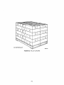
PACKAGING; .......................................................... 9-1
APPENDIX A
MACHINE LEVEL CODE INFORMATION .................................... A-I
APPENDIX B
ORDERING INFORMATION .............................................. B-1
ii
LIST OF FIGURES
Figure
Number
1-1
1-2
1-3
1-4
1-5
1-6
1-7
1-8
1-9
2-1
2-2
2-3
2-4
2-5
3-1
3-2
3-3
4-1
6-1
6-2
6-3
6-4
6-5
6-6
6-7
6-8
6-9
6-10
6-11
6-12
6-13
6-14
6-15
6-16
6-17
7 -1
7 -2
7 -3
7 -4
7 -5
7 -6
7 -7
7 -8
7 -9
7-10
7 -11
8-1
8-2
8-3
9-1
9-2
Title
Page
SA810/860 Half-Height Floppy Disk Drive ................................. 1-0
SA810/860 Functional Diagram ........... . ............................ 1-5
Track Access Timing, Standard Seek ...................................... 1-6
Track Access Timing, Buffered Seek ....................................... 1-7
Read Initiate Timing . . . . . . . . . . . . . . . . . . . . . . . . . . . . . . . . . . . . . . . . . . . . . . . . . . . 1-7
Read Signal Timing (FM Encoding) . . . . . . . . . . . . . . . . . . . . . . . . . . . . . . . . . . . . . . . . 1-8
FM and MFM Code Comparisons ......................................... 1-8
Write Initiate Timing ................................................... 1-9
SA810/860 General Control and Data Timing Requirements .................... 1-10
SA810/860 Interface Connections ........................................ 2-2
Interface Signal Driver/Receiver .......................................... 2-3
Index Timing ........................................................ 2-5
Sector Timing ....................................................... 2-5
DC Power Profile ..................................................... 2-7
Interface Connectors- Physical Locations .................................. 3-1
Jl Connector Dimensions .............................................. 3-2
J2/P2 Connector ..................................................... 3-2
Physical Dimensions ................................................... 4-2
Data Pattern. . . . . . . . . . . . . . . . . . . . . . . . . . . . . . . . . . . . . . . . . . . . . . . . . . . . . . . . . 6-1
Bit Cell ............................................................. 6-1
Byte ............................................................... 6-1
Data Bytes .......................................................... 6-2
FM and MFM Encoding ................................................ 6-4
. SA810/860 Hard Sector Recording Format (FM) ............................. 6-4
MFM Track Format Comparison .......................................... 6-5
MFM Index Pre Address Mark ........................................... 6-6
Index Address Mark FM ................................................ 6-6
MFM Index Address Mark .............................................. 6-7
10 Address Mark FM .................................................. 6-7
MFM 10 Address Mark ................................................. 6-7
MFM Pre ID/Data Address Mark ......................................... 6-8
Data Address Mark FM . . . . . . . . . . . . . . . . . . . . . . . . . . . . . . . . . . . . . . . . . . . . . . . . . 6-8
Deleted Data Address Mark FM .......................................... 6-8
MFM Data Address Mark ............................................... 6-9
MFM Deleted Data Address Mark ......................................... 6-9
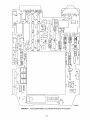
PCB Component Locations (P /N 25227 and 25247) . . . . . . . . . . . . . . . . . . . . . . . . . . 7-3
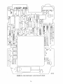
PCB Component Locations (P /N 25249) ................................... 7-4
External Write Current Option ........ . . . . . . . . . . . . . . . . . . . . . . . . . . . . . . . . . . . 7-5
Disk Change Timing ................................................... 7-5
Disk Change Circuit ................................................... 7-6
Side Selection Using Direction Select ...................................... 7-6
Side Selection Using Drive Select ......................................... 7-7
Motor On Without Selecting Drive Circuit . . . . . . . . . . . . . . . . . . . . . . . . . . . . . . . . . . . 7-8
Motor On by Opt. Motor On and Drive Select Circuit ........................... 7-9
Radial Ready Circuit. .................................................. 7-10
Write Protect Circuit ................................................... 7-10
Loading the SA810/860 ............................................... 8-1
Diskette Write Protect . . . . . . . . . . . . . . . . . . . . . . . . . . . . . . . . . . . . . . . . . . . . . . . . . . 8-2
Write Protect Notch Specifications ........................................ 8-2
SA810/860 Packaging ................................................ 9-1
Pallet Loading ....................................................... 9-2
iii
LIST OF TABLES
Table
Number
2-1
3-1
7-1
A-I
B-1
Title
Page
DC Power Requirements ...............................................
Recommended Jl Connectors ...........................................
Customer Cut/Add Trace Options ........................................
Machine Level Code Information .........................................
Ordering Information ..................................................
2-7
3-2
7-2
A-I
B-1
ABBREVIATIONS / MNEMONICS
AM
Address Mark
MFM
Modified FM
CRC
Cyclic Redundancy Check
MLC
Machine Level Code
CRT
Cathode-ray Tube
PCB
Printed Circuit Board
DS
Drive Select
PLL
Phase Locked Loop
FM
Frequency Modulation
SEP
Separated
10
Index
VFO
Variable Frequency Oscillator
LED
Light Emitting Diode
WG
Write Gate
ABOUT THIS MANUAL
This manual (P /N 39216-2) supersedes all earlier manuals. All earlier editions may be discarded.
While every effort has been made to ensure that the information provided herein is correct, please notify us in the
event of an error or inconsistency. Direct any comments on the form at the back of this manual to:
Shugart
Technical Publications
475 Oakmead Parkway
Sunnyvale, CA 94086
(408) 733-0100
iv
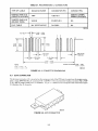
FIGURE 1.1. SA810/860 HALF·HEIGHT FLOPPY DISK DRIVE
1·0
SECTION I
INTRODUCTION
1.1
GENERAL DESCRIPTION
The compact SA810 single-sided and SA860 double-sided half-height 8-inch floppy disk drives offer a reliable, low
cost, high performance solution for OEM data storage applications which require maximum capacity in the smallest
space possible. The SA810/860 drives are half the height of the Shugart SA801 floppy disk drive, fit in comfortably with a CRT, require no ac voltage, and offer up to 1.6 megabytes of unformatted capacity.
The SA810/860 offers the follOWing standard features:
a.
b.
c.
d.
e.
f.
g.
h.
i.
j.
k.
1.
m.
n.
o.
p.
q.
r.
s.
t.
u.
v.
w.
Half-height sizing: 2.31 in. (59 mm) high by 8.55 in. (217 mm) wide by 12.00 in. (305 mm) deep
Interface and media compatibility with Shugart SA801/851 disk drives
Low heat dissipation
Fast access time {3 ms track to track}
Quiet operation
Low media wear due to low mass head
Rapid start dc drive motor--Iess than one revolution {eliminates ac requirements}
Phase-Locked Loop Crystal Referenced Motor Speed Control
Media compatible with SA801/851 plus IBM 3740
Single or double density
0.8/1.6M Bytes (unformatted capacity)
Write protect and programmable door lock for improved data security
Internal write current switching
TRUE READY alerts the system that the drive is ready to send or receive data
Buffered seek
Single or multiple drive dc Motor On control
Multiple jumper options
Shugart's proprietary Bi-Compliant read/write heads with straddle erase elements
Extended reliability
Activity light
Solid die cast chassis
Light weight
Inline dc and I/O connectors
The SA810/860 provides the best solution to the user looking for a compact, low cost, and reliable 8-inch floppy
disk drive. The SA810/860 is the most versatile disk drive on the market. This drive is backed by an engineering
department that is recognized as the largest, most experienced group in the entire floppy industry. The SA810/860
is the ultimate solution for small business systems, intelligent terminals, personal computer systems, and program
storage equipment.
1.2
1.2.1
SPECIFICATIONS SUMMARY
Performance Specifications
Capacity
Unformatted
Per Disk
Per Surface
Per Track
SA810
Single/Double Density
SA860
Single/Double Density
400/800 k bytes
400/800 k bytes
5.2/10.4 k bytes
0.8/1.6 M bytes
400/800 k bytes
5.2/10.4 k bytes
1-1
IBM Format
(128 byte sectors)
Per Disk
Per Surface
Per Track
Transfer Rate
Latency (average)
Access Time
Track to Track
Settle Time
One Track Seek & Settle
Average (including settle)
Motor Start Time
Worst Case
Typical
1.2.2
SA860
Single/Double Density
250/500 k bytes
250/500 k bytes
3.3/6.66 k bytes
250/500 k bits/sec
83 ms
500/1000 k bytes
250/500 k bytes
3.3/6.6t) k bytes
250/500 k bits/sec
83 ms
3
13
16
89
ms
ms
ms
ms
3
13
16
89
ms
ms
ms
ms
165 ms
120 ms
165 ms
120 ms
360 rpm
3268/6536 bpi
360 rpm
3408/6816 bpi
6536 fci
48 tpi
77
1
FM/MFM
6816 fci
48 tpi
154
1
FM/MFM
SA100/102
SAI01/103
SA120
SA150
SA151
SA122
Functional Specifications
Rotational Speed
Recording Density
(inside track)
Flux Density
Track Density
Tracks
Index
Encoding Method
Media Requirements
Soft Sectored
32 Sector Hard Sectored
Alignment Diskette
1.2.3
SA810
Single/Double Density
Physical Specifications
Environmental Limits
Ambient Temperature:
Relative Humidity:
Maximum Wet Bulb:
Operating
Shipping
50° to 115°F (9.9° to 46.1 °C)
20% to 80%
85 OF (29.4 °C)
-40° to 144°F (-40° to 62.2°C)
1 % to 95%
no condensation
Storage
-8° to 122<?F (-22.2° to 50°C)
1 % to 95%
no condensation
DC Voltage Requirements:
+ 24. 00 ± 2.4 V dc @ 1. 0 A typ, 1. 7 A max., 100 m V ripple.
+5.00 ± 0.25 V de @ 0.7 A typ, 1.0 A max., 50 mV ripple.
NOTE
If the stepper motor is energized by the controller during the single motor start-up time, the drive will exceed the + 24 V de current specification of 1. 7 A maximum. Under this condition, the current specification is 2.2 A maximum.
1-2
Mechanical Dimensions
Width = 8.55 in (217 mm)
Height = 2.31 in (59 mm)
Depth = 12.00 in (305 mm)
Weight = 7lbs (3 kg)
Mounting
Top loading
Diskette Horizontal Label Up/Down
Diskette Vertical Label Left/Right
Power Dissipation:
10 watts (34 BTU/hr) Standby
28 watts (96 BTU/hr) Typical
50 watts (171 BTU/hr) Maximum
1.2.4 Reliability Specifications
Mean Time Between Failure: 10,000 Power On Hours under typical usage.
Preventive Maintenance: Not required.
Mean Time to Repair: 30 Minutes
Component Life: 5 years
Error Rates:
1 per 109 bits read
Soft Read Errors:
1 per 10 12 bits read
Hard Read Errors:
1 per 106 seeks
Seek Errors:
Media Life:
Passes per Track: 3.5 x 10⁶
Insertions: 30,000 +
1.3
FUNCTIONAL CHARACTERISTICS
The 810/860 floppy disk drives consist of:
a.
b.
c.
d.
1.3.1
Read/Write and Control Electronics
Drive Mechanism
Precision Track Positioning Mechanism
Read/Write Head (s)
Electronics
The electronics are packaged on one PCB which contains:
a.
b.
c.
d.
e.
f.
g.
h.
i.
j.
k.
1.
m.
n.
Index Detector Circuits (Sector/Index for Hard Sectored Media)
Head Position Actuator Driver
Read/Write Amplifier and Transition Detector
Write Protect
Drive Select Circuits
Spindle Motor Control
Data/Clock Separation Circuits (FM Only)
Drive Ready Detector Circuit
Drive True Ready Detector Circuit
Side Select Circuit (Used on SA860 only)
In Use and Door Lock Circuits
Internal and External Write Current Switching
Power On Reset Circuit
Activity LED
1-3
1.3.2
Drive Mechanism
The Head Positioning Actuator moves the read/write head{s} to the desired track on the diskette. The head{s} is
loaded onto the diskette when the door knob is closed. If no diskette is inserted when the door knob is closed, the
heads will not touch each other.
The dc drive motor under phase locked loop speed control (using an integral tachometer) rotates the spindle at 360
rpm. A contracting collet/spindle assembly provides precision media positioning and clamping to ensure data interchange. A diskette ejector places the diskette within reach of the operator when the diskette is unclamped.
1.3.3 Positioning Mechanism
The read/write head assembly is accurately positioned through the use of a precision HeliCam V-groove lead
screw with a flat nut follower which is attached to the head carriage assembly. Precise track location is accomplished
as the lead screw is rotated in discrete increments by a stepper motor.
1.3.4 Read/Write Heads
The proprietary head {s} is a single element ceramic read/ write head with straddle erase elements to provide erased
areas between data tracks. Thus, normal interchange tolerances between media and drives will not degrade the
signal to noise ratio and diskette interchangeability is ensured.
The read/write head{s) is mounted on a carriage which is located on precision carriage ways. The diskette is held in
a plane perpendicular to the read/write head (s) by a platen located on the base casting. This precise registration
assures perfect compliance with the read/write head{s}. The read/write head{s} is in direct contact with the
diskette. The head surfaces have been designed to obtain maximum signal transfer to and from the magnetic surface of the diskette with minimum head/diskette wear due to the low mass suspension system.
1.3.5
Recording Formats
The format of the data recorded on the diskette is totally a function of the host system. This format can be designed
around the user's application to take maximum advantage of the total available bits that can be written on anyone
track.
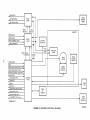
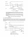
Figure 1-2 provides a functional diagram of the SA810/860. For a detailed discussion of the various recording formats, refer to Section VI.
1.4
1.4.1
FUNCTIONAL OPERATIONS
Power Sequencing
Applying dc power to the SA810 or SA860 can be done in any sequence; however, during power up, the WRITE
"GATE line must be held inactive or at a high level. After application of dc power, a 90 ms delay should be introduced before a seek operation or before the control output signals are valid. After powering on, the initial position of
the read/write heads with respect to the data tracks on the media is indeterminant. In order to assure proper positioning of the read/write heads after power on and internal write current SWitching at the proper track, a STEP
OUT operation should be performed until the TRACK 00 line becomes active (recalibrate).
1.4.2
Drive Selection
Drive selection occurs when the DRIVE SELECT line in the drive is activated. Only the drive with this line active
will respond to input lines or gate output lines. Under normal operation, the DRIVE SELECT line enables the input
and output lines, starts the spindle motor, locks the door, and lights the Activity LED on the front of the drive.
1.4.3 Motor On
In order for the host system to read or write data, the dc drive motor must be turned on. In the standard configuration, this is accomplished by activating the line DRIVE SELECT. A 165 ms delay must be introduced after activating this line (or the TRUE READY line may be monitored) to allow the motor to come up to speed before
reading or writing can be accomplished. All motors in a daisy chain configuration can be turned on with the optional MOTOR ON line or the spindle motor may be activated when both MOTOR ON and DRIVE SELECT are
present. Refer to paragraphs 7.8 and 7.9.
1-4
READ DATA
READ
LOGIC
SEP DATA (FM)
-.
f.-
SEP CLOCK (FM)
WRITE
PROTECT
ASSM
~
DRIVE
SELECT
SIDE
SELECT
...
WRITE DATA
WRITE GATE
-
WRITE
LOGIC
WRITE CURRENT (OPT)
DISKETTE
STEPPER
ACTUATOR
_ WRITE PROTECT
H.
~
I
TRACK
40
j
I'
R/WO
R/W1
SIDE
SELECT
POWER
ON
RESET
R/W HEAD
ASSM .
~
.\ .
~
cJ,
.
·SIDE SELECT
MOTOR
DOOR
CLOSED
SWITCH
STEP
INDEX/
SECTOR
DETECTOR
DIRECTION/ *SIDE SELECT (OPT.)
DRIVE/*SIDE SELECT (OPT.)
MOTOR ON (HEAD LOAD) (OPT.L
IN USE (OPT.)
TWO SIDED (OPT.)
TRACK 00
.
I
t
CONTROL
LOGIC
... INDEX
-p
SECTOR
-
READY/TRUE READY (OPT.)
TRUE READY (OPT.)
...
~
IN USE
LED
TRACK
00
SENSOR
_ DISK CHANGE (OPT.)
.
ALTERNATE I/O (2 lines)
*SA860 ONLY
FIGURE 1·2. SA810/860 FUNCTIONAL DIAGRAM
DOOR
LOCK
SOLENOID
39216·02·A
In the standard configuration, the host system turns off the motor by deactivating the DRIVE SELECT line. This
should be done if the drive has not received a new command within 2.6 seconds (16 revolutions of diskette) after
completing the execution of a command. This will ensure maximum motor and media life. Also, the 2.6 second
delay function can be done by the drive by jumpering the optional Motor Off delay. Refer to paragraph 7.10.
1.4.4 Track Accessing
Seeking the read/write heads from one track to another is accomplished by:
a.
Activating DRIVE SELECT line.
b.
Selecting desired direction utilizing DIRECTION SELECT line.
c.
WRITE GATE being inactive.
d.
Pulsing the STEP line.
Multiple track accessing is accomplished by repeated pulsing of the STEP line until the desired number of steps
have been input. Each pulse on the STEP line will cause the read/write heads to move one track either in or out
depending on the DIRECTION SELECT line. Head movement is initiated on the leading edge of the STEP pulse.
Pulses received at less than a 3 ms period, but greater than 15 p,S, will be stored in a buffer which will then issue step
commands to the drive stepper motor at a 3 ms pulse rate. Pulses received at greater than a 3 ms period will step
the drive at the same rate they are received. The first step begins upon receipt of the first step pulse.
1.4.5 Step Out
With the DIRECTION SELECT line at a plus logic level (2.5 V to 5.25 V), a pulse on the STEP line will cause the
read/write head(s) to move one track away from the center of the disk. The pulse(s) applied to the STEP line must
have the timing characteristics shown in figure 1-3 or figure 1-4.
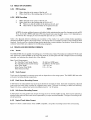
1.4.6 Step In
With the DIRECTION SELECT line at a minus logic level (0 V to 0.4 V), a pulse on the STEP line will cause the
read/write heads to move one track closer to the center of the disk. The pulse(s) applied to the STEP line must
have the timing characteristics shown in figure 1-3 or figure 1-4.
DC POWER
-I--------------~u~-------------
DRIVE SELECT
I
--------------~i~2------------------
DIRECTION SELECT _ _ _ _
I
____
STEP
~
I
i~
~
IN
-I1--11'S
~~S _I
1-16 ms MIN
---------~
11'5
MI~ ~ ~
3 ms MIN"
OUT
1-
11'5 MIN
-I r-
-1
11'5 MIN
~-1---3 ms MIN"
*3 ms is the minimum frequency for a standard seek. Pulses received at less than a 3 ms frequency
will go into a buffered seek mode. See figure 1-4.
39216·03·A
FIGURE 1·3. TRACK ACCESS TIMING, STANDARD SEEK
1-6
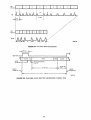
DC POWER
I~--------------~l~l---------------
DRIVE SELECT
I
r--- -
------_.......' - - -I
OUT
DIRECTION SELECT _ _ _1_ _ __
~
STEP
--1~1:1
~----------------
.s
90 ms
MIN
1 /ls
LJlJ
MIN~
rI
15"s MIN"
r-2.~ ms MAX
.~
~ 15/l8 MIN**
I
2.9 ms MAX"
* After the last step pulse has been issued the drive may be deselected. The drive ignores any
change to the DIRECTION SELECT line when no further step pulses are received. This frees the
controller to issue instructions to other drives while the first drive completes the step commands
stored in the buffer.
* * Pulses received at less than a 3 ms period will be stored in a buffer which will then issue step commands to the drive stepper motor at a 3 ms pulse rate. Pulses received at greater than a 3 ms period will step the drive at the same rate they are received. The first step begins upon receipt of the
first step pulse.
39216·31
FIGURE 1·4. TRACK ACCESS TIMING, BUFFERED SEEK
1.4.7
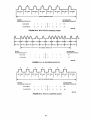
Side Selection (SA860 Only)
Head selection is controlled via the I/O signal line designated SIDE SELECT. A plus logic level on the SIDE
SELECT line selects the read/write head on the side a surface of the diskette. A minus logic level selects the side 1
read/write head. When switching from one side to the other, a 100 JLS delay is required after SIDE SELECT
changes state before a read or write operation can be initiated. Figure 1-5 shows the use of SIDE SELECT prior to a
read operation.
~~------------------------------~u~---------DC POWER
DRIVE SELECT
I
'--------------------------------------------~l~~------------
STEP
SIDE SELECT
(SA860 ONLY)
.--------------------------------~l~~---------------
1-100 "s
-----------------------------~?~~-------------
WRITE GATE
VALID READ DATA - - - - - - - - - - - - - - - - - -
*Or when TRUE READY comes active.
FIGURE 1·5. READ INITIATE TIMING
1-7
39216-04
1.4.8 Read Operation
Reading data from the SA810/860 drive is accomplished by:
a.
Activating DRIVE SELECT line.
b.
Selecting head (SA860 only).
c.
WRITE GATE being inactive.
The timing relationships required to initiate a read sequence are shown in figure 1-5. These timing specifications are
required in order to guarantee that the position of the read/write head has stabilized prior to reading. The timing of
READ DATA (FM) is shown in figure 1-6.
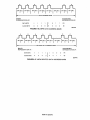
4.00 itS
NOM
READ DATA
I
A
I
SEP DATA
B
I
A
I
A
I
U I
~
SEP CLOCK
l.--200 ± 50 ns
I
LJ
~I ~200
A
B
=
=
U
I
U
A
B
U
I
U
± 50ns
LEADING EDGE OF BIT MAY BE ± 400 ns FROM ITS NOMINAL POSITION.
LEADING EDGE OF BIT MAY BE ± 200 ns FROM ITS NOMINAL POSITION ..
39216·05
FIGURE 1·6. READ SIGNAL TIMING (FM ENCODING)
The encoding scheme of the recorded data can be FM or MFM. The first of these, FM, provides single-density
recording. The superior efficiency of MFM permits the bit cell period to be half that of the FM code, thereby providing double-density recording. Differences among FM and MFM encoding are concerned with the use of clock
bits in the write data stream.
FM encoding rules specify a clock bit at the start of every bit cell. MFM encoding rules allow clock bits to be omitted
from some bit cells, when either the preceding bit cell or the current bit cell contains a data bit. See figure 1-7.
a
o
o
o
BIT
CELLS
D
D
D
D
FM
--..
2F
~
MFM
FIGURE 1·7. FM AND MFM CODE COMPARISONS
1-8
D
In both of these encoding schemes, clock bits are written at the start of their respective bit cells and data bits at the
center of their bit cells.
The timing of the read signals, READ DATA, SEPARATED DATA, and SEPARATED CLOCK are shown in
figure 1-6 (FM encoding).
In the standard SA810/860, data separation of FM data is performed by the drive electronics. Data bits are
presented to the controller on the SEP DATA line and clock bits are presented on the SEP CLOCK line. In systems
using MFM encoding, data separation is performed outside the drive. In such cases, the READ DATA line carries
both clock bits and data bits. Separation of MFM encoded read data should be controlled by a phase-locked loop
circuit.
For additional information regarding the use of MFM encoding, refer to paragraph 6.2.
1.4.9 Write Operation
Writing data to the SA810/860 is accomplished by:
a.
Activating DRIVE SELECT line.
b.
Selecting head.
c.
Activating WRITE GATE line.
d.
Pulsing WRITE DATA line with data to be written.
e.
Head current switching.
The timing relationships required to initiate a write data sequence are shown in figure 1-8. These timing specifications are required in order to guarantee that the read/write head position has stabilized prior to writing.
Write data encoding can be FM or MFM. If MFM is used, the write data should be precompensated to counter the
effects of bit shift. The amount and direction of compensation required for any given bit in the data strea'm depends
on the pattern it forms with nearby bits.
For more details regarding data encoding and formatting for SA810/860 drives, refer to Section VI.
DC POWER
DRIVE
SELECT
I--
90 ms MIN
-----I
I
I
1-
'65 ms MIN1
STEP
SIDE SELECT
(SA860 ONLY)
-I----.U
r-9~~S~--1~ I !--------11
16 ms MIN'
100
I(S MIN
r-i
I_--------------~
WRITE GATE
WRITE DATA
r
-I
i-------..U
* Or
4
'SMIN
U
u
when TRUE READY comes active
39216·07·A
FIGURE 1·8. WRITE INITIATE TIMING
1-9
1.4.10 Sequence Of Events
The timing diagram shown in figure 1-9 illustrates the necessary sequence of events with associated timing restrictions for proper operation.
DC POWER
~90ms MIN
VALID CONTROL
AND OUTPUT SIGNALS 90
ms
MIN
DRIVE SELECT
----.
I
II
I
SIDE SELECT
(SA860 ON L Y)
1_
r-
I
*r--,
,
STEP
1 s
1 M)N
m~
90
MIN
TRUE READY
II
~
r-
*,--'
I ___
~\~
,I
...L.'
~I---\:~\~-------
MAX
~S
SS
{m~t S~ _II T--..l---\S\oS--------.
HMIN~
I ILn
..
NOTE 2~
,
100 ;.--~
I
DIRECTION
SELECT
ss
~500mSMAX
1 /ls
~ ~
-.J t....MIN
1
Mf~
....
I
16
~ 1 /ls MIN
~S
tn.J~----\'t----~NOTE2~16ms
l.-
ms-.i
II ~6II~INm~1MI~r------J--·LI~- - - - " SI ' " S - - I..
I I
~
rI
I...
r-16 ms
WRITE GATE
I
I
SS
MIN
100 •• MIN
WRITE DATA
J.oI-f----~----''--- NOTE
~
L16 ~.
1-
VALID READ
DATA SIGNAL
MIN
l=tnfWJ
---:"'-~-NO-TE
1
;;
~
4 /ls M IN
lnf1ru~I-~
r-
50 /ls MIN
\~
NOTE 1:
165 ms minimum delay must be introduced after DRIVE SELECT to allow time for the dc motor to
reach 360 rpm or the optional TRUE READY line must be monitored.
NOTE 2:
If performing standard seeks, the minimum frequency is 3 ms between steps. If utilizing the drive in
the buffered seek mode of operation the frequency shall be 15 p..s to 2.9 ms between pulses.
* After
the last step pulse has been issued, the drive may be deselected. The drive ignores any change to
the DIRECTION SELECT line when no further step pulses are received. This frees the controller to
issue instructions to other drives while the first drive completes the step commands stored in the
buffer.
39216·08·A
FIGURE 1·9. SA810/860 GENERAL CONTROL AND DATA TIMING REQUIREMENTS
1-10
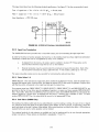
SECTION II
ELECTRICAL INTERFACE
2.1
INTRODUCTION
The interface of the SA810/860 Diskette Drive can be divided into two categories:
a.
b.
Signal
Power
The following paragraphs provide the electrical definition for each line. See figure 2-1 for all interface connections.
2.2
SIGNAL INTERFACE
The signal interface consists of two categories:
a.
b.
Control
Data Transfer
All lines in the signal interface are digital in nature and either provide signals to the drive (input), or provide signals
to the host (output), via interface connector Pl/ J1.
2.2.1
Input Lines
There are twelve signal input lines. Nine are standard and three are user installable options (refer to Section VII).
The input signals are of three types. those intended to be multiplexed in a multiple drive system, those not intended
to be multiplexed. and those which will perform the multiplexing.
The input signals which are intended to do the multiplexing are:
a.
b.
c.
d.
DRIVE
DRIVE
DRIVE
DRIVE
SELECT
SELECT
SELECT
SELECT
1
2
3
4
The input signals to be multiplexed are:
a.
b.
c.
d.
e.
SIDE SELECT
DIRECTION SELECT
STEP
WRITE GATE
WRITE DATA
The input signals which are not multiplexed are:
a.
b.
c.
MOTOR ON (May be optionally multiplexed. Refer to paragraph 7.9.)
IN USE
EXTERNAL WRITE CURRENT SWITCH
2-1
MAX FEET
10 FT FLAT RIBBON OR
20 FT TWISTED PAIR
SA81 01860
HOST
J1
EXTERNAL WRITE CURRENT SWITCHING'
2
1
TRUE READY'
8
7
TWO SIDED' +
DISK CHANGE'
SI DE SELECT' +
10
9
12
11
14
13
IN USE'
16
MOTOR ON' (HEAD LOAD)
15
18
17
INDEX
20
19
READY
22
21
SECTOR
24
DRIVE SELECT 1 (SIDE SELECT OPT) +
DRIVE SELECT 2 (SIDE SELECT OPT) +
DRIVE SELECT 3 (SIDE SELECT OPT) +
2:3
26
25
28
27
30
29
DRIVE SELECT 4 (SIDE SELECT OPT) +
32
DIRECTION SELECT (SIDE SELECT OPT) +
31
34
33
STEP
36
WRITE DATA
WRITE GATE
TRACK 00
WRITE PROTECT
READ DATA
35
38
37
40
39
42
41
44
4"
46
45
SEP DATA
SEP CLOCK
48
47
50
49
~
...... +5 V DC
3
X
+5 V RETURN
......
J2
4
"" +24 V DC
1
X+ 24 V RETURN
2
'"
~
-
5
am
DC -~.fT.
GND
FRAME GND
-=-
TWISTED PAIR
39216·09
'JUMPER ENABLED ALTERNATE I/O LINES.
+ SA860 ONLY
FIGURE 2·1. SA810/860 INTERFACE CONNECTIONS
2-2
The input circuit lines have the following electrical specifications. See figure 2-2 for the recommended circuit.
True
=
False
= Logical one = Vin
Logical zero
=
Vin ± 0.0 to + 0.4 V @ lin
± 2.5 to
+ 5.25 V
@
=
lin
40 rnA (max)
= 250 f-tA (open)
Input Impedance = 220/330 ohms
MAX 10 FEET
RIBBON OR 20
FEET TWISTED
PAIR
I
+5V
7414
39216·10
FIGURE 2·2. INTERFACE SIGNAL DRIVER/RECEIVER
2.2.2
Input Line Termination
The SA810/860 has been provided with a removable resistor pack for terminating the eight input lines.
In order for the drive to function properly, the last drive on the interface must have these eight lines terminated.
Termination of these lines can be accomplished by either of two methods:
a.
As shipped from the factory, the resistor pack is installed in location U9. These packs can be
removed from all drives except the last one on the interface.
b.
External termination may be used provided the terminator is beyond the last drive. Each of the
lines should be terminated by using a 220/330 ohm, 1/4 watt resistor, pulled up to + 5 V dc.
The same removable resistor pack is also prOVided for terminating the optional input lines.
2.2.3
Drive Select 1·4
DRIVE SELECT, when activated to a logical zero level, enables the multiplexed I/O lines, starts the spindle motor,
energizes the stepper motor, locks the door, and lights the activity LED. In this mode of operation, only the drive
with this line active will respond to the input lines and gate the output lines.
Four separate input lines, DRIVE SELECT 1, DRIVE SELECT 2, DRIVE SELECT 3, and DRIVE SELECT 4, are
prOVided so that up to four drives may be multiplexed together in a system and have separate DRIVE SELECT
lines. Traces DS1, DS2, DS3, and DS4 have been prOVided to select which DRIVE SELECT line will activate the
interface signals for a unique drive. As shipped from the factory, a shorting plug is installed on DSl. To select
another DRIVE SELECT line, this plug should be moved to the appropriate OS pin.
2.2.4
Side Select (SA860 Only)
This interface line defines which side of a two-sided diskette is used for reading or writing. An open circuit, or logical
one, selects the read/write head on the side 0 surface of the diskette. A short to ground, or logical zero, selects the
read/write head on the side 1 surface of the diskette. When switching from one head to the other, a 100 f-tS delay is
required before any read or write operation can be initiated.
Two optional methods of side selection are available and can be implemented by the user through appropriate
jumper connections. These options are described in paragraphs 7.5 and 7.6.
2-3
2.2.5
Direction Select
This interface line is a control signal which defines the direction of motion the read/write heads will take when the
STEP line is pulsed. An open circuit, or logical one, defines the direction as "out" and if a pulse is applied to the
STEP line, the read/write heads will move away from the center of the disk. Conversely, if this input is shorted to
ground, or a logical zero level, the direction of motion is defined as "in" and if a pulse is applied to the STEP line,
the read/write heads will move towards the center of the disk. If buffered stepping is used, any changes to the
DIRECTION SELECT line will be ignored by the drive during the time step pulses(s) are not input.
A jumper-selectable option is available which allows the DIRECTION SELECT line to be time shared for both the
DIRECTION SELECT and SIDE SELECT functions. That is, during head positioning operations, the DIRECTION
SELECT line controls direction of head motion. During read or write operations, the DIRECTION SELECT line
determines which head is selected. Details regarding the implementation of this option are provided in paragraph
7.5.
NOTE
A 16 ms delay must be introduced when changing direction (i.e., the last step-in pulse to the first
step-out pulse or vice versa).
2.2.6
Step
This interface line is a control signal which causes the read/write heads to move with the direction of motion defined by the DIRECTION SELECT line.
The access motion is initiated on each logical one to logical zero transition or the leading edge of the signal pulse.
For a standard seek, step pulses may be received at a rate of 3 ms minimum time between pulses having 1 P.s
minimum pulse width. Any change in the DIRECTION SELECT line must be made at least 1 P.s minimum before
the leading edge of the STEP pulse. Refer to figure 1-3 for these timings.
a
Buffered stepping may be done by issuing pulse(s) to the drive at a rate of 15 P.s minimum to 2.9 ms maximum time
between pulses having a 1 p'S minimum pulse width. Pulses are stored in a buffer which will issue step commands
to the drive stepper motor at a 3 ms pulse rate. The first step begins upon receipt of the first step pulse. Any
change to the DIRECTION SELECT line during the time step pulse(s) are not input will be discounted by the drive.
See figure 1-4 for these timings.
2.2.7
Write Gate
The active state of this signal (logical zero) enables WRITE DATA to be written on the diskette. The inactive state
(logical one) enables the read data logic (SEPARATED DATA, SEPARATED CLOCK, and READ DATA) and
stepper logic. Refer to figure 1-8 for WRITE INITIATE timing information.
2.2.8
Write Data
This interface line provides the data to be written on the diskette. Each transition from a logical one level to a logical
zero level will cause the current through the read/write head to be reversed, thereby writing a data bit. This line is
enabled by WRITE GATE being active. See figure 1-8 for timing information.
2.2.9
Motor On (Alternate Input)
This customer installable option, when enabled by jumpering trace MO or MMO and activated to a logical zero
level, will activate the dc spindle motor. Refer to paragraphs 7.8 and 7.9 for uses and method of installation.
2.2.10
In Use (Alternate Input)
This customer installable option will turn on the Activity LED and lock the door. Refer to paragraph 7.7 for uses
and method of installation.
2.2.11
External Write Current Switch (Alternate Input)
Reference paragraph 7.2.
2-4
2.2.12 Output Lines
There are nine standard output lines from the SA810/860 with two optional output lines and two alternate outputs
available. The output signals are driven with an open collector output stage capable of sinking a maximum of 40
rnA at a logical zero level or true state with a maximum voltage of 0.4 V measured at the driver. When the line
driver is in a logical one or false state, the driver is off and the collector current is a maximum of 250 p.A. See figure
2-2 for the recommended circuit.
2.2.13 Track 00
The active state of this signal, or a logical zero, indicates when the read/write heads of the drive are positioned at
track 00 (the outermost track) and the access circuitry is driving current through phase one of the stepper motor.
This signal is at a logical one level, or false state, when the read/write heads of the selected drive are not at track
00.
.
2.2.14 Index
This interface signal is prOVided by the drive once each revolution of the diskette (166.67 ms) to indicate the beginning of the track. Normally, this signal is a logical one and makes the transition to the logical zero level for a period
of 0.2 to 2.4 ms once each revolution. The timing for this signal is shown in figure 2-3.
To correctly detect INDEX at the control unit, INDEX should be false at DRIVE SELECT time; that is, the controller
should see the transition from false to true after the drive has been selected. INDEX pulses will only be provided
when the diskette is up to speed.
U
0.2 to 2.4 ms
=u=
39216·11
FIGURE 2·3. INDEX TIMING
2.2.15
Sector (Hard Sector Only)
When a hard sectored diskette is inserted and up to speed, this interface signal is provided by the drive 32 times
each revolution. Normally, this signal is a logical one and makes the transition to a logical zero for a period of 0.4
ms each time a sector hole on the diskette is detected. Figure 2-4 shows the timing of this signal and its relationship
to the INDEX pulse.
I~
SECTOR
INDEX
U
~ 15.20
U
U
I
~
U
~-
:!:
0.30 ms
SS
U
rU
~
0.4 ± 0.2 ms
SS
2.60 ± 0.15 ms
39216·12
FIGURE 2·4. SECTOR TIMING
2.2.16 Ready
This interface signal indicates that two index holes have been sensed after properly inserting and clamping a
diskette. Three holes have to be sensed for two sided diskettes. Whenever the door knob is rotated to the closed
position, the spindle motor will be activated by the drive until the READY signal is generated.
2-5
If a single sided diskette is installed, READY will be active (logical zero) when SIDE a is selected, but false (logicalone) when SIDE 1 is selected. Conversely, if a two-sided diskette is installed, READY will be active when either
side of the diskette is selected.
For additional methods of using the READY line, refer to paragraph 7.11.
NOTE
READ DATA, SEP DATA, and SEP CLOCK are only present when DRIVE SELECT and TRUE
READY are active (low) and WRITE GATE is inactive (high).
2.2.17
Read Data
This interface line provides the "raw data" (clock and data together) as detected by the drive electronics. Normally,
this signal is a logical one level and becomes a logical zero level for the active state. See figure 1- 6 for the timing and
bit shift tolerance within normal media variations.
2.2.18
Sep Data
This interface line furnishes the data bits as separated from the "raw data" by use of the internal FM data separator.
Normally, this signal is a logical one level and becomes a logical zero level for the active state. See figure 1-6 for the
timing.
2.2.19
Sep Clock
This interface line furnishes the clock bits as separated from the "raw data" by use of the internal FM data separator.
Normally, this signal is a logical one level and becomes a logical zero level for the active state. See figure 1-6 for the
timing.
2.2.20
Write Protect
This interface signal is prOVided by the drive to give the user an indication when a write protected diskette is installed. This signal is a logical zero level when it is protected. Under normal operation, the drive will inhibit writing with
a protected diskette installed in addition to notifying the interface.
For other methods of using write protect. refer to paragraph 7.13.
2.2.21
True Ready
This output (pin 8) signals that the drive is ready to handle data. The line will come true (active low) when the
diskette is up to speed, all seek functions have been completed, and the READY line is active (refer to paragraph
2.2.16). It is recommended that this signal be used in place of motor start and seek complete timers.
2.2.22
Disk Change (Optional Output)
Reference paragraph 7.4.
2.2.23
Two Sided (Optional Output)
Reference paragraph 7.3.
2.2.24 Alternate I/O Pins
These interface lines (pins 4 and 6) have been provided for use with customer installable options. Refer to Section
VII for methods of use.
2.3 POWER INTERFACE
The SA81a and SA86a require only dc power for operation. DC power to the drive is provided via P2/ J210cated
on the component side of the PCB near the stepper motor. The two dc voltages, their specifications, and their
P2/ J2 pin designators are outlined in table 2-1. The specifications outlined on current requirements are for one
drive. For multiple drive systems, the current requirements are a multiple of the maximum current times the
number of drives in the system. See figure 2-5 for the dc power requirements during various operations.
2-6
2.4 FRAME GROUNDING
The drive must be frame grounded to the host system to ensure proper operation. If the frame of the drive is not
fastened directly to the frame of the host system with good ac ground. a wire from the system ac frame ground
must be connected to the drive. For this purpose. a faston tab_is provided on the drive where a faston connector
can be attached or soldered. The tab is AMP PIN 61664-1 and its mating connector is AMP PIN 60972-1.
a
TABLE 2·1. DC POWER REQUIREMENTS
P2 PIN
DC VOLTAGE
1
+24 V DC·
2
+ 24 V RETURN··
3
+5V DC
4
+ 5 V RETURN··
5
FRAME GROUND
TOLERANCE
CURRENT
MAX RIPPLE (p to p)
±2.4 V DC
1.7 A MAX
1.0 A MAX
100 mV MAX ALLOWABLE
1.0 A MAX
0.7 A TYP
50 mV MAX ALLOWABLE
±0.25 V DC
• If the stepper motor is energized by the controller during the spindle motor start-up time, the drive
will exceed the + 24 V DC current specification of 1.7 A max. Under this condition, the current
specification is 2.2 A max.
39216-13
•• Returns are tied together at the drive PCB.
1.6
- - - 24 VOLTS
- - - 5VOLTS
TYPICAL
CURRENT
REQUIREMENTS
(AMPS)
1.0
0.1
POWER
ON
MOTOR START
&
DOOR LOCK
RUNNING
SEEKING @
STEPPER
3 ms STEP RATE
(POWER DOWN)
WRITING
STAND
BY
39216·14·A
FIGURE 2·5. DC POWER PROFILE
2-7/2-8 (blank)
SECTION III
PHYSICAL INTERFACE
3.1
INTRODUCTION
The electrical interface between the SA810 or SA860 and the host system is via two connectors. The first connector, J 1, provides the signal interface and the second connector, J2, provides the dc power.
This section describes the physical connectors used on the drive and the recommended connectors to be used with
them. Refer to figure 3-1 for connector locations.
3.2
Jl jPl CONNECTOR
Connection to J 1 is through a 50 pin PCB edge connector. The dimensions for this connector are shown in figure
3-2. The pins are numbered 1 through 50 with the even numbered pins on the component side of the PCB and the
odd numbered pins on the non-component side. Pin 2 is located on the end of the PCB connector closest to the dc
connector and is labeled 2. A key slot is provided between pins 4 and 6 for optional connector keying.
The recommended connectors for PI are shown in table 3-1.
P2 CONNECTOR
~ AMP PIN 1·480763
~
FRAME CONNECTOR
AMP PIN 60972-1
P1 CONNECTOR
SCOTCH FLEX
- - - PIN 3415·0001 or
AMP PIN 1·583718·1
39216·15
FIGURE 3-1. INTERFACE CONNECTORS - PHYSICAL LOCATIONS
3-1
TABLE 3·1. RECOMMENDED J1 CONNECTORS
TYPE OF CABLE
MANUFACTURER
CONNECTOR PIN
CONTACT PIN
TWISTED PAIR, #18
(CRIMP OR SOLDER)
AMP
1·583718·1
583616-5 (CRIMP)
583854-3 (SOLDER)
TWISTED PAIR, #18
(SOLDER TERM.)
VIKING
3VH25/1 J N·5
NA
FLAT CABLE
3M "SCOTCH FLEX"
3415·0001
NA
39216·16
KEY SLOT
~
IIj.--
0.036 ± 0.004
(0091 ± 0010)
,...
1
0.450 ± 0.010
(1.143 ± 0.025)
ii
I
~~
I
~ f-0~~O,~?M
0.050 NOM
(0.127)
~~.--_ _ _ _ _ _ _ _ _
,... . .50
._ _ __
1...-....-0.063 (0.160)
r--- NOM (2X)
0.100 NOM--+(0.254)
2.575 ± 0.010
(6.541 :+ 0.025)
---------.....-t
BOARD THICKNESS 0.062 ± 0.007
(0.157 ± 0.017)
NOTE:
x.xxx ± x.xxx = in.
(x.xxx ± x.xxx) = em
50574·19
FIGURE 3·2. J1 CONNECTOR DIMENSIONS
3.3
J2/P2 CONNECTOR
The dc power connector. J2. is mounted on the component side of the PCB and is located near the stepper motor.
J2 is a 5 pin AMP Mate-N-Lok connector PIN 1-350945-0. The recommended mating connector (P2) is AMP
PIN 1-480763 utilizing AMP pins PiN 350689-1. J2. pin 1. is labeled on the component side of the PCB. Figure
3-3 illustrates the J2 connector.
FIGURE 3·3. J2/P2 CONNECTOR
3·2
SECTION IV
DRIVE PHYSICAL SPECIFICATIONS
4.1
INTRODUCTION
This section describes the mechanical dimensions and mounting recommendations for the SA810/860.
4.2 MECHANICAL DIMENSIONS
See figure 4-1 for the dimensions of the SA810/860.
4.3 MOUNTING
The SA810/860 is capable of being mounted any position.
4.4 STACKING DUAL DRIVES
When using the bottom mounting holes of the SA810/860, a second unit may be mounted on top of the first using
a mounting kit (P /N 51592). This method of mounting is not recommended when high shock or vibration levels
are expected.
4-1
0.47± ±0.76
0.03mm) - - .
(11.94
-
LI
r
o
I
~
....--
I
0.33 ± 0.01
(8.38 :!: 0.25 mm)
~I
---L
101
0
I
....-_-:_-_-___I_-__ _\LJ
1.15 ± 0.04
(29.21 ± 1.0 mm)
I
f
Q.
2.31 ± 0.03
(58.4 ± 0.76 mm)
II FAC~:~:~.02
(2O.32:!: 1.0 mm)
8.00 ± 0.04 -+-
~(2x)
(20.32 :!: 0.5 mm)
(2x)
1.865 ± 0.03
(211.32 mm x 6.35 mm)
8.32
UNC.2~8~
0.25
0.33 \
(8.38 mm)
I.~~~~;::===-~o~;;;;;;~f:n --...
r
-.-- ;----, ~9 ± 0.03
£,
2.465 ± 0.05
(62.61
1.27 m m ) -
7.47 ± 0.4
(189.7 I
± 0.10 mm)
[Q
(45.44 ± 0.76 mm)
LED
I
,
I
! 8.55 ± 0.03
1(217.17 mm
~=::;~=~~~~~~ ~:!:
I...
0.38 ± 0.03 .... ,..(9.7 ± 0.76 mm)
1.
t
I
...
. (47: ± 0.76 mm) +
DEEP ----1-----.\(6·gl~1 mil. g~.6+~E;)
I
..--
3.50 ± 0.04
(88.9 ± 1.0 mm) ..
12.00 ± 0.02
((305 mm ± 0.5 mm)
r
DOOR KNOB
mm)
1.00 ± 0.04
(25.4 ± 1.0 mm
I
LJ
0.165 NOM
..--(4.19 mm)
1.357 ± 0.03
DISK SLOT
(34.47 ± 0.76 mm)
NOTES
a. Measurements are in inches unless otherwise specified.
b. Faceplate allows 1/8" (3.17 mm) clearance on all four sides for bezels.
FIGURE 4·1. PHYSICAL DIMENSIONS
4-2
39216·18
SECTION V
ERROR RECOVERY
5.1 WRITE ERRORS
If an error occurs during a write operation, it will be detected on the next revolution by doing a read operation,
commonly called a write check. To correct the error, another write and write check operation must be done. If the
write operation is not successful after 10 attempts, a read operation should be attempted on another track to determine if the media or the drive is failing. If the error still persists. the disk should be considered defective and
discarded.
5.2 READ ERRORS
Most errors that occur will be soft errors; that is, by performing an error recovery procedure, the data will be
recovered.
Soft errors are usually caused by:
a.
b.
c.
Airborne contaminants that pass between the read/write head and the disk. These contaminants
will generally be removed by the cartridge self-cleaning wiper.
Random electrical noise which usually lasts for a few microseconds.
Small defects in the written data and/or track not detected during the write operation which may
cause a soft error during a read.
The following procedures are recommended to recover from soft errors:
a.
b.
c.
d.
Reread the track 10 times or until such a time as the data is recovered.
If data is not recovered after using step (a). access the head to the adjacent track in the same
direction previously moved, then return to the desired track.
Repeat step (a).
.
If data is not recovered, the error is not recoverable.
5.3 SEEK ERRORS
Seek errors are detected by reading an 10 field after the seek is completed. The 10 field contains the track address.
If a seek error is detected, the host system should issue a recalibrate operation (step out until Track 00 line goes active) and seek back to the original track.
5-1/5-2 (blank)
SECTION VI
RECORDING FORMAT
6.1
RECORDING FORMAT (SINGLE DENSITY)
The format of the data recorded on the diskette is totally a function of the host controller. Data is recorded on the
diskette using frequency modulation as the recording mode. i.e., each data bit recorded on the diskette has an
associated clock bit recorded with it. This is referred to as FM encoding. Data written on and read back from the
diskettes takes the form shown in figure 6-1. The binary data pattern shown in figure 6-2 represents a "10 1."
6.1.1
Bit Cell
As shown in figure 6-2, the clock bits and data bits (if present) are interleaved. By definition. a bit cell is the period
between the leading edge of one clock bit and the leading edge of the next clock bit.
CLOCK BITS
CLOCK BITS
DATA BIT
(IF PRESENT)
f.-
BIT CELL
JLJi)-----?u;L
~I
I
DATA BITS
50574·26
FIGURE 6-2 .. BIT CELL
FIGURE 6·1. DATA PATTERN
CDC
BIT CELLI-:IT
o
D
BIT CELL
2
CDC
CDC
C
C
CE~ -.. 1
50574·27
- - -
CDC
,- - - - -
-
BIT CELL BIT CELL BIT CELL BIT CELL BIT CELL
3
5
4
7
6
LSB
MSB
--'"
BYTE
BINARY REPRESENTATION OF:
CLOCK BITS
o
o
DATA BITS
o
o
1 '
HEXADECIMAL
REPRESENTATION OF:
DATA BITS
. CLOCK BITS
50574·28
FIGURE 6·3. BYTE
6-1
6.1.2
Byte
A byte, when referring to serial data (being written onto or read from the disk drive), is defined as eight consecutive
bit cells. The most significant bit cell is defined as bit cell 0 and the least significant bit cell is defined as bit cell 7.
When reference is made to a specific data bit (Le., data bit 3), it is with respect to the corresponding bit cell (bit cell
3).
During a write operation, bit cell 0 of each byte is transferred to the disk drive first with bit cell 7 being transferred
last. Correspondingly, the most significant byte of data is transferred to the disk first and the least significant byte is
transferred last.
When data is being read back from the drive, bit cell 0 of each byte will be transferred first with bit cell 7 last. As with
writing, the most significant byte will be transferred first from the drive to the user.
Figure 6-3 illustrates the relationship of the bits within a byte. Figure 6-4 illustrates the relationship of the bytes for
read and write data.
BYTE
I I
0
2
3
4
5
6
7.
8
9
10
11
12
13
14
15
1 16 r~:E 1
t
1
BIT CELL 7 OF BYTE 17 IS
LAST DATA TO BE SENT TO
THE DRIVE WHEN WRITING
AND FROM THE DRIVE
WHEN READING
BIT CELL 0 OF BYTE 0 IS
FIRST DATA TO BE SENT
TO THE DRIVE WHEN
WRITING AND FROM THE
DRIVE WHEN READING
50574·29
FIGURE 6·4. DATA BYTES
6.2
RECORDING FORMAT (DOUBLE DENSITY)
Double capacity can be obtained by use of MFM (modified frequency modulation) rather than FM (frequency
modulation) which is the standard method of encoding data on the diskette.
The differences between FM and MFM encoding are shown in figure 6-5. Note that MFM results in a 1 to 1 relationship between the flux chan.ges per inch and the data bits per inch recorded on the diskette. This also results in a
doubling of the data transfer rate, from 250 to 500 k bytes, when compared to FM.
Data error rate performance equal to standard capacity diskettes using FM encoding can be achieved by using:
a.
b.
c.
The SA810/860 diskette drive with its proprietary ceramic/ferrite read/write head.
Phase locked loop (VFO) data separator.
Write precompensation.
Provision of the phase locked loop data separator and write precompensation circuitry is the responsibility of the
user of the SA810/860 diskette drive.
Shugart will provide design information, as required, to SA810/860 users who desire to incorporate double
capacity diskette drives in their products.
The bit cell for MFM encoded data is one half the duration of the bit cell for FM encoded data. Also, unlike FM,
MFM bit cells do not always contain a clock bit at the leading edge. This lack of a clock bit makes data separation
more complex. Also, the window size is half the FM window size, which results in less tolerance to bit shift. The only
reliable method to separate MFM encoded data is through use of a phase locked loop (VFO) type of data separator.
The VFO, once synchronized, tracks the data and generates clock and data windows. This improves the bit shift
tolerance over the conventional "hard" data separators commonly used in FM recording which use windows of fixed timing.
6-2
6.3 RULES OF ENCODING
6.3.1
FM Encoding:
a.
b.
6.3.2
Writes data bits at the center of the bit cell.
Writes clock bits at the leading edge of the bit cell.
MFM Encoding:
a.
b.
Writes data bits at the center of the bit cell.
Writes clock bits at the leading edge of the bit cell i;:
•
There is no data bit written in the previous bit cell, and
•
There will be no data bit written in the present bit cell.
NOTE
In MFM, the write oscillator frequency is doubled while maintaining the same flux changes per inch as FM.
Thus, the bit cell in MFM is half that in FM. Data transfer rate is also doubled, since a 1 to 1 relationship exists between flux changes per inch and data bits per inch (2 to 1 in FM).
Index is the physical detector indicating one revolution of the media. It is used to initiate format operations,
generate the READY signal in the storage device, and ensure that one complete revolution of the media has been
searched. It is also used for a deselect storage device signal after a certain number of revolutions. Some of the more
common format fields are explained in the following paragraphs.
6.4 TRACKS AND RECORDING FORMATS
6.4.1
Tracks
The SA810/860 drive is capable of recording up to 77/154 tracks of data. The tracks are numbered 0-76 for each
side. Each track is made available to the read/write heads by accessing the head with a stepper motor and carriage
assembly, and selecting the desired side of the diskette.
Basic Track Characteristics:
No. Data Bits/Track Single Density
No. Data Bits/Track Double Density
Index Pulse Width
Index/Sector Pulse Width
(Hard Sectored Only)
6.4.2
41.664 bits (5208 bytes)
83,328 bits (10,416 bytes)
1.8 ± 0.6 ms
0.4 ± 0.2 ms
Track Format
Tracks may be formatted in numerous ways and are dependent on the using system. The SA810/860 use index
and sector recording formats respectively.
6.4.3
Hard Sector Recording Format
In this format, the using system may record up to 32 sectors (records) per track. Each track is started by a physical
index pulse and each sector is started by a physical sector pulse. This type of recording is called hard sectoring.
Figure 6-6 shows a typical hard sector recording format for 1 of 32 sectors.
6.4.4
Soft Sector Recording Format
In this format, the using system may record one long record or several smaller records. Each track is started by a
physical index pulse and then each record is preceded by a unique recorded identifier. This type of recording is called soft sectoring.
6.4.5
Typical Track Index Format
Figure 6-7 shows a track format, which is IBM compatible, using index recording format with soft sectoring.
BIT
CELLS
0
I
I
I
I
12F
D
D
0
D
1F
D
0
0
D
FM
-1::01-
4p,sec
~
~
/
""
""
/
/
~
"
~
/
~
/
BIT.
CELLS
I I I
1
1
1
I
0
1
o
I
~
0
0
,
;fI
""
"
;fI
;fI
MFM
D
D
0
D
C
C
, "
D
;fI
;fI
1F
r~
----'1
4/3F
1"-
50574·30
FIGURE 6·5. FM AND MFM ENCODING
. ~1400 ItS
~± 200
~~OO~
1__ ..
,( s r -
_________________
~~
~I-----r~------------~--~----~
DATA
SYNC
15 BYTES 4---.....1
WRITE
TURN ON
CLOCK
DATA IDENTIFIER1 BYTE
104----- 130 BYTES
~---------5.2
± 0.30
15 BYTES
----~...... NOM
WRITE
TURN OFF
ms-·--------~
50574-31
FIGURE 6·6. SA810/860 HARD SECTOR RECORDING FORMAT (FM)
6-4
~_____I_ND_E_X_________________________________________________________________
MFM 10416 BYTES - - - - - - - - - - - - - - - -.....
REPEAT FOR EACH RECORD
G.A
III
I·~~~~ ~:~ ~M
m
~Nel ~ci'~M
G1
4E
00
4E
00
80
12
3
50
12
80
12
3
50
12
80
12
3
50
12
FC
m
I
AM
1,0
[II
IeRe I
G'
8]
I
---------+t
I
DATA
SYNC
16~~AI
AM
AM
III
m
DATA I CRC
I
WG
OFF
I
G3
G4B
4E
00
40
8]
4E
4E
4
22
12
1024
2
115
654
BYTES/8 REC.
3
4
22
12
512
2
83
400
BYTES/15 REC.
3
4
22
12
53
598
BYTES/26 REC.
FE
3
256
4E
DATA
UPDATE WRITE
OJ
ill
m
m
rn
3 BYTES C2 WITH UNIQUE CLOCK PATTERN 14
3 BYTES A1 WITH UNIQUE CLOCK PATTERN OA
TRACK NUMBER, HEAD NUMBER, SECTOR, RECORD LENGTH
GENERATED BY CRC GENERATOR WHICH SHOULD BE EQUIVALENT TO CCITT VH1
1 BYTE OF FB OR F8
50574·32
FIGURE 6·7. MFM TRACK FORMAT COMPARISON
Gap 1-
G4A is from the physical index address mark sync and allows for physical index variation, speed
variation, and interchange between storage devices.
Sync is a fixed number of bytes for separator synchronization prior to the address mark. It includes a minimum of two bytes plus worst case separator sync up requirements.
Index Pre Address Mark (MFM) is three bytes of C2 with unique clock bits not written per the
encode rules. See figure 6-8.
Index Address Mark (FM) is a unique byte to identify the index field and is not written per the
encode rules. See figure 6-9.
Index Address Mark (MFM) is one byte of FC and is written per the encode rules. See figure
6-10.
Gl is from index address mark to 10 field address mark sync.
10 Field -
Sync is a fixed number of bytes for separator synchronization prior to the address mark. It includes a minimum of two bytes plus worst case separator sync up requirements.
10 Pre Address Mark (MFM) is three bytes of A 1 with unique clock bits not written per the
encode rules. See figure 6-8.
10 Address Mark (FM) is a unique byte to identify the 10 field and is not written per the encode rules. See figure 6-11.
10 Address Mark (MFM) is one byte of FE and it is written per the encode rules. See figure
6-12.
10 is a four byte address containing track number, head number, record number, and record
length.
CRC is two bytes for cyclic redundancy check.
Gap 2-
Gap 2 is from IDCRC to data address mark sync and allows for speed variation, oscillator
variation, and erase core clearance of IDCRC bytes prior to write gate turn on for an update
write.
6-5
Data Field -
Sync is a fixed number of bytes for separator synchronization prior to the address mark. Includes a minimum of two bytes plus worst case separator sync up requirements.
Pre Data Address Mark (MFM) is three bytes of Al with unique clock bits not written per
the encode rules. See figure 6-13.
Data Address Mark (FM) is a unique byte to identify the Data Field and is not written per
the encode rules. See figures 6-14 and 6-15.
Data Address Mark (MFM) is one byte of FB or F8 and it is written per the encode rules.
See figure 6-16 and 6-17.
Data is the area for user data.
CRC is two bytes for cyclic redundancy check.
WG OFF (Write Gate Off) is one byte to allow for the WRITE GATE turn off after an update write.
Gap 3-
Gap 3 is from WG OFF to the next 10 AM sync and allows for the erase core to clear the
Data Field CRC bytes, speed and write oscillator variation, read preamplifier recovery time,
and system turn around time to read the following ID Field.
Gap 4-
G48 is the last gap prior to physical index and allows for speed and write oscillator variation
during a format write and physical index variation.
D
D
n
Jl
BIT
~ELL I BIT ~ELL I BIT CELL
2
n
I
D
C
C
BIT CELL
3
I
BIT
~ELL
n
I
BIT
n
~ELL
BIT
~ELL
I
BIT CELL
7
INDEX PRE ADDRESS MARK
HEXADECIMAL
REPRESENTATION OF:'
BINARY
REPRESENTATION OF:
o
DATA BITS
o
CLOCK BITS
o
o
o
o
o
o
o
o
C2
o
14
50574·33
FIGURE 6·8. MFM INDEX PRE ADDRESS MARK
D
C
BIT CELL
7
C
BIT CELL
a
D
BIT CELL
1
D
BIT CELL
2
C
D
D
BIT CELL
3
BIT CELL
4
CDC
BIT CELL
5
C
BIT CELL
6
BIT CELL
7
BIT CELL
a
~-----------------------------------------INDEXADDRESSMARKBYTE--------------------------------~~
BINARY
REPRESENTATION OF:
HEXADECIMAL
REPRESENTATION OF:
a
DATA BITS
CLOCK BITS
1
o
a
a
FC
D7
50574·34
FIGURE 6·9. INDEX ADDRESS MARK FM
6-6
D
BIT
D
I
~ELL
BIT
D
D
I
~ELL
BIT
~ELL
I
BIT
i
D
ELL
D
BIT CELL
4
C
I
~ELL
BIT
BIT
~ELL
I
BIT
~ELL
~-----------------------INDEXADDRESSMARK----------------~------~
BINARY
REPRESENTATION OF:
HEXIDECIMAL
REPRESENTATION OF:
o
DATA BITS
o
CLOCK BITS
o
o
o
o
o
FC
o
01
50574·35
FIGURE 6·10.MFM INDEX ADDRESS MARK
C
CDC
D
D
D
D
CDC
D
C
C
C
BIT CELL 7 BIT CELL 0 BIT CELL 1 BIT CELL 2 BIT CELL 3 BIT CELL 4 BIT CELL 5 BIT CELL 6 BIT CELL 7 BIT CELL 0
~------------------IDADDRESSMARKBYTE------------------~
BINARY
REPRESENTATION OF:
HEXADECIMAL
REPRESENTATION OF:
o
DATA BITS
o
o
CLOCK BITS
FE
o
C7
50574·36
FIGURE 6·11.10 ADDRESS MARK FM
D
BIT CELL
o
D
BIT
~ELL
D
I
BIT
~ELL
D
D
BIT CELL
BIT CELL
4
3
D
D
BIT
~ELL
I
I
BIT
~ELL
BIT CELL
7
~-----------------------MFMIDADDRESSMARK--------~------------~~
BINARY
REPRESENTATION OF:
HEXADECIMAL
, REPRESENTATION OF:
DATA BITS
CLOCK BITS
o
o
o
o
o
o
o
o
FE
o
00
50574·37
FIGURE 6·12. MFM 10 ADDRESS MARK
6-7
D
D
C
n
Jl
BIT CELL
0
BIT CELL
1
BIT
~ELL
I
BIT
~ELL
n
I
D
C
BIT
~ELL
I
BIT
~ELL
n
I
BIT
~ELL
rL
I
BIT CELL
7
PRE ADDRESS MARK
BINARY
REPRESENTATION OF:
HEXADECIMAL
REPRESENTATION OF:
DATA BITS
0
0
CLOCK BITS
0
0
0
0
0
0
A1
0
0
0
OA
50574·38
FIGURE 6·13. MFM PRE ID/DATA ADDRESS MARK
..
~
~
- ..
-..
~
--
...
BIT CELL 7 BIT CELL 0 BIT CELL 1 BIT CELL 2 BIT CELL 3 BIT CELL 4 BIT CELL 5 BIT CELL 6 BIT CELL 7 BIT CELL 0
..
•
DATA ADDRESS MARK BYTE
HEXADECIMAL
REPRESENTATION OF:
BINARY
REPRESENTATION OF:
o
DATA BITS
o
o
CLOCK BITS
FB
o
C7
50574·66
FIGURE 6·14. DATA ADDRESS MARK FM
C
..-
C
D
- ..
C
. ..
D
0
~
-
D
D
..
-
,.
..
~
C
C
C
C
-
.
-
...
~
C
..
~IT CELL 7 BIT CELL 0 BIT CELL 1 BIT CELL 2 BIT CELL 3 BIT CELL 4 BIT CELL 5 BIT CELL 6 BIT CELL 7 BIT CELL 0
•
DELETED DATA ADDRESS MARK BYTE
BINARY
REPRESENTATION OF:
HEXADECIMAL
REPRESENTATION OF:
o
DATA BITS
CLOCK BITS
o
o
o
o
o
FIGURE 6·15. DELETED DATA ADDRESS MARK FM
6-8
F8
C7
50574·39
D
BIT
D
D
~ELL
I
BIT
I
~ELL
BIT
D
I
~ELL
BIT
i
ELL
I
BIT
D
D
D
I
~ELL
BIT
~ELL
I
BIT
~ELL
I
BIT ?ELL
I"'~
__- - - - - - - - - - - DATA ADDRESS MARK - - - - - - - - - - -......
HEXADECIMAL
REPRESENTATION OF:
BINARY
REPRESENTATION OF:
o
DATA BITS
o
CLOCK BITS
o
o
o
o
FB
o
o
o
00
50574-67
FIGURE 6·16. MFM DATA ADDRESS MARK
D
C
BIT
~ELL
I
BIT
~ELL
I
BIT
~ELL
I
BIT
i
D
D
D
D
ELL
I
BIT
~ELL
I
BIT
~ELL
I
C
BIT
~ELL
I
BIT ?ELL
......- - - - - - - - - - D E L E T E D DATA ADDRESS MARK - - - - - - - - - -....
BINARY
REPRESENTATION OF: .
HEXADECIMAL
REPRESENTATION OF:
o
DATA BITS
CLOCK BITS
o
o
o
o
o
o
o
o
Fa
03
50574-40
FIGURE 6·17. MFM DELETED DATA ADDRESS MARK
6-9/6-10 (blank)
SECTION VII
CUSTOMER INSTALLABLE OPTIONS
7.1
INTRODUCTION
The SA810/860 Can be modified by the user to function differently than the standard method outlined in Sections I
and II. These modifications can be implemented by adding or deleting connections and by use of the alternate I/O
pins. Some options are capable of being connected by use of a shorting plug, Shugart PIN 15648 or AMP PIN
53013-2. This section will discuss a few examples of modifications and how to install them. The modifications
discussed in the following paragraphs are:
a.
b.
c.
d.
e.
f.
g.
h.
i.
j.
k.
I.
External Write Current Switch
Two-Sided Status Output (SA860 only)
Disk Change Option
Side Select Option Using Direction Select (SA860 only)
Side Select Option Using Drive Select (SA860 only)
In Use Alternate Input
Motor On Without Selecting Drive
Motor On by Optional Motor On and Drive Select
Motor Off Delay
Radial Ready
Stepper Power Down
Write Protect Optional Use
Table 7-1 summarizes these options and the component designators indicating their PCB location in figure 7-1 and
7-2.
7-1
TABLE 7·1. CUSTOMER CUT/ADD TRACE OPTIONS
TRACE
DESIGNATOR
U9
DESCRIPTION
SHIPPED FROM FACTORY
OPEN
TERMINATIONS FOR MULTIPLEXED INPUTS
SHORT
PLUGGED
SI
INTERNAL WRITE CURRENT SWITCH
SE
EXTERNAL WRITE CURRENT SWITCH
TR
TRUE READY OUTPUT
PLUGGED
RADIAL TRUE READYt
X
RTR
PLUGGED
X
2S
TWO-SIDED STATUS OUTPUT***
X
DC
DISK CHANGE OPTION
X
S1
SIDE SELECT OPTION USING DIRECTION SELECT***
X
S2
SIDE SELECT INPUT* * *
PLUGGED
S3
SIDE SELECT OPTION USING DRIVE SELECT* * *
1B,2B,3B,4B
SIDE SELECT OPTION USING DRIVE SELECT***
X
ALTERNATE INPUT-IN USE
X
D
X
MS
MOTOR ON FROM DRIVE SELECT*
MO
ALTERNATE INPUT-MOTOR ON*
X
ALTERNATE INPUT-MULTIPLEXED MOTOR ON*t
X
MOTOR OFF DELAY
X
MMO
MD
PLUGGED
R
READY OUTPUT
X
RR
RADIAL READY
X
PLUGGED
SR
STANDARD READYt
MT
MODIFIED TRUE READYt (OUTPUTS TRUE READY ON PIN 22)
DS1
DRIVE SELECT 1 INPUT
DS2,3,4
Y
X
PLUGGED
X
DRIVE SELECT 2,3,4 INPUT
DOOR LOCK/ACTIVITY LIGHT ACTIVATED FROM MOTOR ONt
PLUGGED
z
DOOR LOCK/ACTIVITY LIGHT ACTIVATED FROM DRIVE SELECTt
X
PD
STEPPER POWER DOWN
X
WP
INHIBIT WRITE WHEN WRITE PROTECTED
NP
ALLOW WRITE WHEN WRITE PROTECTED
X
TS
DATA SEPARATION OPTION SELECT**
X
X
*MOTOR ON is the complement of HEAD LOAD on the SA801 and SA851 disk drives. The only difference in the
operation of MOTOR ON compared with HEAD LOAD is· that MOTOR ON requires a 165 ms minimum delay (or
TRUE READY must be monitored) before RIW activity is begun. HEAD LOAD on the SA801 and SA851 requires 35
ms or 50 ms minimum delay.
* *The SA81 0/860 offers an optional data separator which properly separates data and clock bits thmugh the softsectored IBM standard format and address mark area. Trace "TS" offers the optional separator.
* * * Applies to SA860 only.
tAvailable on PCB PIN 25249 only.
39216-19-A
7-2
CZ
C3
CI
~
C54
RI7
RI5
RI8
AI
All
A4
~ ~~~ ~
LZ
LI
-c=J-c:J- C"
-c=J-
S
C4
C7
AZ4
-
Rll
RZI
RZ5
C5
Cil
CI8
RI"
CI9
..
R84
0
C8
CAI5-cft
/
C.
~rn
-c=J- .
RZ8
-c:JA,..
[}grn
[}grn
JiLJ
~D
-c:J-
CSO
1==t ::
RlO
R~Il:;; ~ ~~ .
<To
10
RSS
=t::=j:
B
(
/ ..
'0
-
CRI7
Cl3
R,I
~
RSZ
CZ4
c..
~==============~----------------
~ .o:mt---_-----4II}1111111I111~1(J~
FIGURE 7·1. PCB COMPONENT LOCATIONS (PIN 25227 AND 25247)
7-3
•
Rl8-c=J-
~
iO
fI=
lJ
=~ i==t
=t==i= ( ,
RlO
RS9
CRI7
-B-
D
/
..
@I...
.
FIGURE 7·2. PCB COMPONENT LOCATIONS (PIN 25249)
7-4
7.2
EXTERNAL WRITE CURRENT SWITCH
This option permits write current switching via the optional WRITE CURRENT SWITCHING interface line (pin 2).
When the interface signal is activated to a logical zero level. the lower value of the write current is selected. Selecting this option replaces internal write current switching at track 40.
To enable external write current sWitching. move the shorting plug at trace SI to the SE position. See figure 7-3.
+5V
..... STANDARD TRACE
1I1'}II DELETED TRACE
. - . ADDED OR JUMPERED
TRACE
2
EXTERNAL WRITE
CURRENT SWITCH - " l f r - - - -...
TO WRITE
-TRACK 4 0 - -...........
/,.....--+---1"'"----'
SI
~---I CURRENT REF
39216·21.
FIGURE 7·3. EXTERNAL WRITE CURRENT OPTION
7.3
TWO-SIDED STATUS (OPTIONAL OUTPUT SA860 ONLY)
When the drive is selected and the diskette is spinning, this line will indicate a logical zero level for two sided media,
and a logical one for single sided media.
To install this option on a standard drive. jumper trace 25.
7.4
DISK CHANGE (OPTIONAL OUTPUT)
This customer installable option is enabled by jumpering trace DC. When DRIVE SELECT is activated, it will provide a true signal (logical zero) onto the interface (pin 12) if. while deselected, the drive has gone from a READY to
a NOT READY (door open) condition. This line is reset on the true to false transition of DRIVE SELECT if the drive
has gone READY. Timing of this line is illustrated in figure 7-4. The circuitry is illustrated in figure 7-5.
ss
-DRV SEL - - - - -
-READY
_ ------Irs
ss
.
I
I
..
ss
-DISK CHG -----J~f"""-- S,S~........j
INTERNAL
ENABLE
({
,j
• READY will not return until two index transitions after DRIVE SELECT (MOTOR ON).
39216·22
FIGURE 7·4. DISK CHANGE TIMING
7-5
+
5V
o
a
C
Q D--------t
12
h..-_ _--II..-..._--*_
-DISK CHG
-READY
-DRVSEL~----------------~------------~~>--------~
39216·23
FIGURE 7·5. DISK CHANGE CIRCUIT
7 _5
SIDE SELECTION USING DIRECTION SELECT (SA860 ONLY)
The SIDE SELECT function can be controlled via the DIRECTION SELECT line, if desired. With this option, the
DIRECTION SELECT line controls the direction of head motion during stepping operations and controls side
(head) selection during read/write operations. To implement this option, simply move jumper S2 to location Sl.
Figure 7-6 illustrates the circuitry.
+ DRIVE SELECT
-SIDE 0
CT
S2
-SIDESELECT----~~~----------------1>Cr-~----------1___~
-SIDE 1
CT
S1
-01 RECTION SELECT _ _ _-+-_ _---(~>---------SIDE SELECT
39216·24
FIGURE 7-6. SIDE SELECTION USING DIRECTION SELECT
7.6
SIDE SELECTION USING DRIVE SELECT (SA860 ONLY)
In systems containing no more than two SA860 drives per controller. each read/write head can be assigned a
separate drive address. In such cases, the four DRIVE SELECT lines can be used to select the four read/write
heads. To implement this option, move jumper S2 to S3 and add a jumper to nB (n = 1, 2, 3, or 4). For example,
the first drive may have jumpers installed at DS 1 and 2B while the second drive has jumpers at DS3 and 4B. With
this jumper configuration installed, the four DRIVE SELECT lines have the following side selection functions:
a of first drive.
a.
DRIVE SELECT 1 selects side
b.
DRIVE SELECT 2 selects side 1 of first drive
c.
DRIVE SELECT 3 selects side
d.
DRIVE SELECT 4 selects side 1 of second drive.
a of second drive.
Figure 7 -7 illustrates the circuitry.
7-6
+5V
1
-DRIVE
SELECT
18
2
28
3
DRIVE
SELECTINT
38
4
48
-SIDE 0
CT
S3
-SIDE 1
CT
39216·25
FIGURE 7·7. SIDE SELECTION USING DRIVE SELECT
7.7
IN USE ALTERNATE INPUT
This alternate input (pin 16) when activated to a logical zero level enables the Activity LED and door lock latch if
the door is closed. If IN USE is low upon deselection, the door remains locked. If IN USE is high upon deselection,
the door unlocks. To install this option, jumper trace D and move the shorting plug at trace Y to the Z position.
7.8 MOTOR ON WITHOUT SELECTING DRIVE
This option is useful in disk to disk copy operations. It allows the user to keep the motor on for all drives, thereby
eliminating the motor start time. The motor is started on each drive via an Alternate I/O (pin 18). Each drive may
have its own MOTOR ON line (Radial or Simplexed) or they may share the same line (Multiplexed). When the
drive is selected, a 1 IlS delay must be introduced or TRUE READY must be monitored before a read or write
operation can be performed.
To install this option on a standard drive, move the shorting plug at trace MS to the MO position. See figure 7-8.
7-7
-DHIVE SELECT 4 --*)(------3-2----~r~--1
-DRIVE SELECT
3 --*)f------3-0-----~~1t---li
-DRIVE SELECT 2
--l)~(----:-:------I~+-I----+r---ll.
-DRIVE SELECT 1 --*-----------~-+-~:-----...----1
~~ ~~ ~~ en
Cl
Cl
Cl
Cl
. .- - - - - I
..
II
..
+5V
MS
OPTIONAL
SIDE SELECT
FROM DRIVE
SELECT
-...t--. -MOTOR ON
NOTE
2
2
--+)ff---- ---::.=
=,~
4
ALTERNATE}
~)(~---It-= = == == =~ :
6
___6___ J1
1/0 PINS
~
~)ff----_.~ ______ .,
I
a =4-= ::.
=
-MOTOR ON
18
-1!~~---18
::
II
II
If the MOTOR ON line is
multiplexed, the terminator
pack at U9 must be removed from each drive except
the last on the line. The
current requirement is the
+ 24 Volt current times
the number of drives on
the line that have MOTOR
ON active.
II
39216·26
FIGURE 7·8. MOTOR ON WITHOUT SELECTING DRIVE CIRCUIT
7.9
MOTOR ON BY OPTIONAL MOTOR ON AND DRIVE SELECT
This option would be advantageous to the user who requires one drive to be selected at all times, but does not wish
to keep the motor on for all drives. In this configuration, the dc spindle motor is controlled from DRIVE SELECT
and the optional MOTOR ON line. The advantage of this option would be that the output control signals could be
monitored without spinning the diskette thereby extending the head and media life. When the system requires the
drive to perform a read or write, the controller would activate the MOTOR ON line (pin 18) which in turn would
activate the spindle motor. After the MOTOR ON line is activated, a 165 ms delay must be introduced or the
TRUE READY line must be monitored before a read or write operation can be performed.
To install this option on a standard drive, move the shorting plug at trace MS to the MMO position. Figure 7-9 illustrates the circuitry.
7.10
MOTOR OFF DELAY
This jumper option delays the spindle motor from turning off for 16 revolutions (2.6 seconds) after the DRIVE
SELECT or optional MOTOR ON signal goes false (high). This allows the user to be able to read or write within 1 p,s
after the drive has been reselected, thereby eliminating the motor start time. This option is advantageous for the
user who wishes to perform copy routines, but does not wish to use the optional MOTOR ON input signal.
To enable the MOTOR OFF DELAY on the standard drive, jumper trace MD.
7-8
-DRIVE SELECT 4
x
-DRIVE SELECT 3
)(
-DRIVE SELECT 2
)(
32
I i
I 1
I I 1
30
28
26
-DRIVE SELECT 1
. . . . STANDARD TRACE
i
.,,111 DELETED TRACE
2·
...... ADDED OR JUMPERED
TRACE
en en en
V~ 11~
en
o
0
.
0
II
0
Ii
+5V
MS
OPTIONAL
SIDE SELECT
FROM DRIVE
SELECT
-.+-......
NOTE
2
2
---+)(~-4---i"~::'==
ALTERNATEJ
~)(E----_.~ =
== =~:
1/0 PINS
~
6
___6____"
4-= ==,\
===
~wr-~-~It~------~I
-MOTOR ON
18
---iE~----18
::
II
II
-MOTOR ON
If the MOTOR ON line is
multiplexed, the terminator
pack at U9 must be removed from each drive except
the last on the line. The
current requirement is the
+ 24 Volt current times
the number of drives on
the line that have MOTOR
ON active.
II
39216-27
FIGURE 7·9. MOTOR ON BY OPT. MOTOR ON AND DRIVE SELECT CIRCUIT
7.11
RADIAL READY
This option enables the user to monitor the READY line of each drive on the interface. This can be useful in detecting when an operator has removed or installed a diskette in any drive. Normally, the READY line from a drive is
only available to the interface when it is selected.
To install this option on a standard drive, the following traces should be deleted or added:
a.
Cut trace RR.
b.
Cut trace R.
c.
Add a wire from R to one of the Alternate I/O pins.
NOTE
One of the drives on the interface may use pin 22 as its READY line, therefore steps band c may
be eliminated on this drive. All the other drives on the interface must have their own READY line,
therefore steps band c must be incorporated.
Figure 7-10 illustrates the circuitry.
7-9
+5V
RR
+ DRIVE SELECT
2:......--••."./'}.II~--*"-...,--"-~~""""""
+ READY
~--------------~__~
R
22
D----------------1~/~/~.~--------~~~
..
~READY
II
II
II
If
2
II
2
li= =-==-=--------*")E
II
II
..
4
I,:' II
II
I~=
4 )(
-:II:11
....-----*"-
6
6
==....-"'--___
- " - -)(
*_
39216·28
FIGURE 7·10. RADIAL READY CIRCUIT
7.12
STEPPER POWER DOWN
If the user wishes to step the drive at a step rate of 6 ms or slower. enabling this option will allow the drive to maintain ~ low noise emission level.
To install this option on a standard drive, jumper trace PD.
7.13
WRITE PROTECT OPTIONAL USE
As shipped from the factory. the write protect feature will internally inhibit writing when a write protected diskette is
installed. With this option installed. a write protected diskette wiWnot inhibit writing, but it will be reported to the interface. This option may be useful in identifying special use diskettes.
To install this option on a drive with the write protect feature. the following traces should be added or deleted.
a.
Cut trace WP.
b.
Connect trace NP.
Figure 7-11 illustrates the circuitry.
-WRITEPROTECl
l~~~~~~~.~~~~~~~~~~~--~lTOINTERFACE
WNPP~:~D-_ _
-f
l~-------~---~
2 TO WRITE CU RRENT
39216·29
FIGURE 7·11. WRITE PROTECT CIRCUIT
7-10
SECTION VIII
OPERATION PROCEDURES
8.1
INTRODUCTION
The SA810/860 was designed for ease of operator use to facilitate a wide range of operator oriented applications.
The following section is a guide for the handling and error recovery procedures on the diskette and diskette drive.
8.2
DISKETTE LOADING AND HANDLING
The diskette is a flexible disk enclosed in a plastic jacket. The interior of the jacket is lined with a wiping material to
clean the disk of foreign material. Figure 8-1 shows the proper method of loading a diskette in the SA810/860
Diskette Storage Drive . To load the diskette. rotate the door knob clockwise and insert the diskette with the label
facing the door knob. Rotate the door knob counter-clockwise to lock the diskette on the drive spindle. The diskette
can be loaded or unloaded with all power on.
NOTE
The diskette cannot be removed when the activity light is lit. The activity light indicates that the
door is locked.
FIGURE 8·1. LOADING THE SA81 0/860 '
8-1
When removed from the drive, the diskette is stored in an envelope. To protect the diskette, the same care and
handling procedures specified for computer tape apply. These precautionary procedures are as follows:
8.2.1
a.
Return diskette to storage envelope whenever it is removed from drive.
b.
Keep diskettes away from magnetic fields and from ferromagnetic materials which might become
magnetized. Strong magnetic fields can destroy recorded data on disk.
c.
Replace storage envelopes when they become worn. cracked, or distorted. Envelopes are designed to protect disk.
d.
Do not write on plastic jacket with lead pencil or ball-point pen. Use felt tip pen.
e.
Heat and contamination from carelessly dropped ashes can damage disk.
f.
Do not expose diskette to heat or sunlight.
g.
Do not touch or attempt to clean disk surface. Abrasions may cause loss of stored data. '
Write Protect:
Shugart 8-Inch Diskettes
The Shugart 8-inch diskettes have the capability of being write protected. The write protect feature is selected by
the slot in the diskette. When the slot is open. it is protected; when covered, writing is allowed. The slot is closed by
placing a tab over the front of the slot, and folding the tab over to cover the rear of the slot. The diskette can then be
write protected by removing the tab. See figure 8-2.
8.2.2
Write Protect:
IBM Diskettes
IBM diskettes are not manufactured with a pre-punched write protect slot.To write protect one of these diskettes, a
slot must be punched out as speCified in figure 8-3. The operation of the write protect is that which is outlined in
paragraph 2.2.20.
FOLD OVER BACK'
OF DISKETTE
TAB
I
o@
I,
~
c:::::>
'---
D
WRITE ENABLED
WRITE PROTECTED
FIGURE 8·2. DISKETTE WRITE PROTECT
0.200 ± 0.010
(0.508 ± 0.025 em)
RADIUS
x.xxx = in.
(x.xxx) = em
~
0.150 ± 0.005
(0.381 ± 0.013 em)
0.075 ± 0.005
(0.191 ± 0.013 em)
1
.©
U
.~
c::::>-"t:.175
±
0.005
(15.685 ± 0.013 em)
~D~----,l
50574·61
FIGURE 8·3. WRITE PROTECT NOTCH SPECIFICATIONS
8-2
50574·60
SECTION IX
PACKAGING
It is suggested that packing material be kept in case the unit must be returned to Shugart for repair. Regardless, the
unit must be individually packaged in comparable packing as shipped to preclude damage in shipping and handling. Damage to the unit as a result of inadequate packaging will void the warranty on the unit.
Figure 9-1 shows how to repackage the disk drive using the original shipping containers. Figure 9-2 illustrates the
pallet pattern and the maximum pallet size to use if reshipped in large quantities.
39216·33.
FIGURE 9·1. SA81 0/860 PACKAGING
9-1
42 UNITS/PALLET
39216·34
FIGURE 9·2. PALLET LOADING
9-2
APPENDIX A
MACHINE LEVEL CODE INFORMATION
Table A-I identifies distinct features or exceptions to the general description of the SA810/860 in this manual.
TABLE A·1. MACHINE LEVEL CODE INFORMATION
MLC NUMBER
0
DESCRIPTION
THE WORST CASE MOTOR START TIME IS 220 ms.
THE MULTIPLEXED MOTOR ON LINE OPTION IS NOT AVAILABLE.
BUFFERED SEEK IS NOT INCLUDED.
TRUE READY IS INVALID FOR THE PURPOSE OF MOTOR-UP-TO-SPEED.
JUMPERS RTR, MMO, SR, MT, Y AND Z ARE NOT INCLUDED.
THE FACEPLATE AND KNOB DESCRIBED IN THE SA810/860 OEM MANUAL 39216-0 IS
INCLUDED.
1
SAME AS MLC 0 EXCEPT THATTHE FACEPLATE AND KNOB ARE AS DESCRIBED IN
THIS MANUAL.
2
SAME AS MLC 1 EXCEPT THAT STATIC CLAMPING AND PCB 25247
ARE INCLUDED.
39216·32.
A-1/A-2 (blank)
APPENDIX B
ORDERING INFORMATION
Table B-1 can be used to construct a part number for a unique drive configuration.
TABLE B·1. SA81 0/860 ORDERING INFORMATION
AB
PRODUCT
LINE
c
OPTION
68
810
o
NONE
AB
PRODUCT
LINE
c
OPTION
69
860
o
NONE
D
D
MODEL
E
OPTION
F
OPTION
810
o
NONE
o
NONE
MODEL
E
OPTION
F
OPTION
860
a
NONE
o
NONE
39224·06
8-1/8-2 (blank)
I II II I
NO POSTAGE
NECESSARY
IF MAILED
IN THE
UNITED STATES
BUSINESS REPLY CARD
First Class Permit No.1 061 S'vale, Ca 94086
Postage will be paid by addressee
Shugart
Attn: Technical Publications
475 Oakmead Parkway
Sunnyvale, Ca 94086
I II II I
BUSINESS REPLY CARD
First Class Permit NO.1 061 S'vale, Ca 94086
Postage will be paid by addressee
Shugart
Attn: Technical Publications
475 Oakmead Parkway
Sunnyvale, Ca 94086
NO POSTAGE
NECESSARY
IF MAILED
IN THE
UNITED STATES
Shugart
I
475 Oakmead Parkway
Sunnyvale, CA 94086
Technical Publications
Suggestion Form
1
We would appreciate your comments and suggestions for improving this publkation
Publicalion No:
Tille:
Dale:
What is your overall rating of this publication?
o Very Good
0
Fair
0 Very Poor
Good
0
Poor
o
Is the material presented effectively?
o Well organized 0 Fully covered 0
o Correct
0
Well illustrated
Clear
Comments:
Please Print: Name, Address and Phone No.
Shugart
I
475 Oak mead Parkway
Sunnyvale, CA 94086
Technical Publications
Suggestion Form
I
We would appreciate your comments and suggestions for improving this publication
Publicalion No:
Tille:
What is your overall rating of this publication?
o Very Good
0
Fair
0 Very Poor
o Good
0
Poor
Comments:
Please Print: Name, Address and Phone No.
Dale:
Is the material presented effectively?
o Well organized 0 Fully covered 0
o Correct
0
Well illustrated
Clear