1
I/O Expansion Bus for 7188X/7188E
User’s Manual
Warranty
All products manufactured by ICP DAS are warranted against
defective materials for a period of one year from the date of
delivery to the original purchaser.
Warning
ICP DAS assume no liability for damages consequent to the
use of this product. ICP DAS reserves the right to change this
manual at any time without notice. The information furnished
by ICP DAS is believed to be accurate and reliable. However,
no responsibility is assumed by ICP DAS for its use, not for
any infringements of patents or other rights of third parties
resulting from its use.
Copyright
Copyright 2002 by ICP DAS. All rights are reserved.
Trademark
The names used for identification only may be registered
trademarks of their respective companies.
I/O Expansion Bus for 7188X/7188E User’s Manual, Jun/2004 v1.4, 7PH-000-14---1
Table of Contents
1.
2.
INTRODUCTION............................................................................................. 5
1.1
WHAT IS THE I/O EXPANSION BUS? ............................................................. 5
1.2
1.3
1.4
USING I-7188 I/O EXPANSION BOARDS: ...................................................... 5
OVERVIEW: ................................................................................................ 5
RECONFIGURING THE 7188XC(D)/7521(D) ................................................. 9
REFERENCE GUIDE.................................................................................... 13
2.1
2.2
3.
4.
WIRE CONNECTION : ................................................................................. 14
3.1
3.2
DIGITAL INPUT WIRE CONNECTION :........................................................... 14
DIGITAL OUTPUT WIRE CONNECTION : ....................................................... 14
3.3
3.4
3.5
VOLTAGE INPUT WIRE CONNECTION: ......................................................... 15
VOLTAGE OUTPUT WIRE CONNECTION:...................................................... 15
CURRENT INPUT WIRE CONNECTION:......................................................... 15
MOUNTING OF I/O EXPANSION BUS ........................................................ 16
4.1
4.2
4.3
4.4
5.
7.
MINIMAL MOUNTING WITH 7-SEGMEMT DISPLAY ........................................... 16
MEDIUM MOUNTING WITHOUT 7-SEG DISPLAY ............................................ 17
MOUNTING WITHOUT CASE ...................................................................... 18
ODM MOUNTING WITHOUT CASE.............................................................. 19
I/O EXPANSION BUS................................................................................... 20
5.1
5.2
5.3
6.
THIS MANUAL CAN ALSO BE FOUND AT :....................................................... 13
SOFTWARE INSTALLATION & DEMO PROGRAMS: ......................................... 13
DEFINITION .............................................................................................. 21
PARALLEL BUS ......................................................................................... 25
SERIAL BUS ............................................................................................. 30
SELECTION GUIDE ..................................................................................... 32
6.1
EXPANSION BOARD FOR PROTOTYPE, TESTING .......................................... 32
6.2
6.3
6.4
6.5
I/O EXPANSION BOARD FOR D/I, D/O, TIMER/COUNTER, PWM................... 32
I/O EXPANSION BOARD FOR A/D, D/A, DI, DO .......................................... 33
I/O EXPANSION BOARD FOR RS-232, RS-422, RS-485, DI, DO ................ 33
I/O EXPANSION BOARD FOR SRAM, FLASH ............................................... 34
X0XX I/O EXPANSION BOARDS................................................................. 35
7.1
7.2
X000 :PROTOTYPE BOARD ....................................................................... 35
X001: PROTOTYPE BOARD ....................................................................... 36
I/O Expansion Bus for 7188X/7188E User’s Manual, Jun/2004 v1.4, 7PH-000-14---2
7.3
7.4
7.5
8.
X002 : PROTOTYPE BOARD ...................................................................... 37
X003: TEST BOARD 1............................................................................... 38
X004: TEST BOARD 2............................................................................... 39
X1XX I/O EXPANSION BOARDS................................................................. 42
8.1
8.2
8.3
8.4
8.5
8.6
8.7
8.8
8.9
8.10
8.11
8.12
9.
X100: DI * 8............................................................................................ 42
X101: DO * 8.......................................................................................... 44
X102: RELAY * 2...................................................................................... 46
X103: ISOLATED DI * 7............................................................................. 48
X104: D/I/O * 8, SINGLE-BIT ..................................................................... 50
X105: D/I/O * 8, 8-BIT ............................................................................. 53
X106: DO *2 OR DI *3............................................................................. 56
X107: DI * 6 AND DO * 7 ......................................................................... 58
X108: PWM * 2 ...................................................................................... 60
X109: PHOTOMOS RELAY * 7.................................................................. 63
X110: 14 CHANNELS D/I .......................................................................... 64
X111: 13 CHANNELS D/O ........................................................................ 65
X2XX I/O EXPANSION BOARDS................................................................. 66
9.1
9.2
9.3
9.4
X200: AD*1 ............................................................................................ 66
X201: AD*4 ............................................................................................ 67
X202: AD*7 ............................................................................................ 69
X203: AD*2 + DO*6 + DI*2 .................................................................... 70
10.
X3XX I/O EXPANSION BOARDS ............................................................. 71
10.1
10.2
10.3
10.4
10.5
10.6
10.7
10.8
10.9
10.10
11.
X300: DA * 2 .......................................................................................... 71
X301: DA * 1 + AD * 1............................................................................ 72
X302: DA * 1 + AD * 1............................................................................ 74
X303: AD*1 + DA*1 + DO*6 + DI*4 ........................................................ 76
X304: AD*3 + DA*1 + DO*4 + DI*4 ........................................................ 78
X305: AD*7 + DA*1 + DO*2 + DI*2 ........................................................ 80
X306: AD*2 ............................................................................................ 82
X307: AD*8 ............................................................................................ 83
X308: AD*4 + DO*6 ............................................................................... 84
X310: AD*2 + DA*2 + DO*3 + DI*3 ........................................................ 86
X4XX I/O EXPANSION BOARDS ............................................................. 88
11.1
X400:TIMER/COUNTER *3 ......................................................................... 88
I/O Expansion Bus for 7188X/7188E User’s Manual, Jun/2004 v1.4, 7PH-000-14---3
12.
X5XX I/O EXPANSION BOARDS ............................................................. 92
12.1
12.2
12.3
12.4
12.5
12.6
12.7
12.8
12.9
12.10
X500: RS232 * 1 .................................................................................... 92
X501: RS232 * 1 .................................................................................... 95
X502: RS232 * 1 .................................................................................... 96
X503: RS232 * 1 .................................................................................... 97
X504: RS232 * 2 .................................................................................... 98
X505: RS232 * 3 .................................................................................... 99
X506: RS232 * 6 .................................................................................. 100
X507: RS422 * 1 + DO*4 + DI*4 .......................................................... 100
X508: RS232 * 1 + DO*4 + DI*4 .......................................................... 103
X509: RS232 * 2 + DO*4 + DI*4........................................................... 105
12.11
12.12
12.13
12.14
X510: RS232 * 1 + DO*5 + DI*5 .......................................................... 107
X511: RS485 * 3 .................................................................................. 109
X512: RS-232 * 4 + RS485 * 1............................................................. 110
X560: RS-232 * 3 + 8 M FLASH ............................................................ 111
13.
X6XX I/O EXPANSION BOARDS ........................................................... 113
13.1
13.2
X600 AND X601 : FLASH ROM............................................................... 113
X607 AND X608: SRAM ........................................................................ 114
I/O Expansion Bus for 7188X/7188E User’s Manual, Jun/2004 v1.4, 7PH-000-14---4
1. Introduction
1.1 What is the I/O Expansion Bus?
The I-7188XA, I-7188XC, I-7188XB, I-7188XG, I-7188EX, I7188EG & 7521 all support I/O expansion buses. The I/O
expansion bus can be used to implement various I/O
functions such as D/I, D/O, A/D, D/A, Timer/Counter, UART,
flash memory, battery backup SRAM & other I/O functions.
Nearly all kinds of I/O functions can be implemented on this
bus.
1.2 Using I-7188 I/O Expansion Boards:
The I-7188X series can plug an I/O Expansion board inside
the main body. To install it, users have to loosen the screw
and remove the shell of I-7188XA / I-7188XC / I-7188XB / I7188EX / I7188XG / I7188EG. The supported I/O expansion
boards are as below. It will be more.
1.3 Overview:
Even though the 7000 family is so powerful, there are some
applications chart cannot be solved, such as:
High speed applications
Special hardware requirement applications
Special software requirement applications
Combine special hardware & software applications
So we developed an I/O expansion bus in the 7188X / 752N /
7188E family to solve all these applications above. The I/O
expansion bus can be used to implement various I/O
functions such as D/I, D/O, A/D, D/A, Timer/Counter, UART,
I/O Expansion Bus for 7188X/7188E User’s Manual, Jun/2004 v1.4, 7PH-000-14---5
flash memory, battery backup SRAM & other I/O functions.
Nearly all kinds of I/O functions can be implemented in
this bus.
The I/O expansion bus includes serial & parallel interface.
The parallel interface is very similar to an ISA bus, so the
user can move the old ISA bus design to the I/O expansion
bus with very little modification. The power consumption table
is given as follows:
CPU Module
7188XC
7188XB / XG
7188EX / EG
140mA@5V
260mA@5V
290mA@5V
Note:
Power consumption of 7-SEG
LED is 140 mA
I/O Expansion
Board
Total Max.
410mA@5V
290mA@5V
260mA@5V
For example:
7188XCD=140+140=280
550 mA@5V
550 mA@5V
550 mA@5V
So I/O=550-280=270 mA max.
Note:The 7188XA(D) supports I/O expansion bus but does not support
user defined pins, so the 7188XA only supports X002, X003, X560,
X600, X601, X607, X608.
I/O Expansion Bus for 7188X/7188E User’s Manual, Jun/2004 v1.4, 7PH-000-14---6
The I/O pins of serial bus are programmable. They can be
programmed as D/I, or D/O. Some pins can be configured to D/I
or D/O or timer input or timer output. There are many serial
interface devices today. The features of these serial devices are
given as follows:
Smaller size compared to parallel devices.
Lower cost compared to parallel devices.
Easier to design for isolation application.
The serial interface of an I/O expansion bus can link to these
serial devices very easily. The combination of serial & parallel
interface makes the I/O expansion bus very easy & powerful for
various industry applications. These are many design examples
given in this manual and all hardware circuit & software driver
sources are OPENING for all user. From these examples, the
users can buy these examples or modify them for their special
requirements. The system design steps are given as follows:
Step 1: List all functions required.
Step 2: For all functions, go to step 3. If all functions are solved
STOP.
Step 3: If this function can be solved by the 7000 module
Go to
step 2 for next function.
Step 4: If this function can be solved by 7188X+X???
Go to step
2 for next function.
Step 5: Now user must design special hardware on the I/O
expansion bus.
Step 6: User writes their special software driver based on this new
hardware.
Step 7: Refer to “7521/7522/7523/24/27 Software User’s manual”
for firmware. Modify & download this firmware into the CPU
module, this module now will work as a customized 7000
module.
Step 8: Go to step 2 for next function.
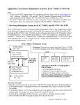
After the above steps, user can combine the standard-7000
modules & customized-7000 modules to solve all applications
in the same RS-485 network. This customized solution diagram is
given as follows:
I/O Expansion Bus for 7188X/7188E User’s Manual, Jun/2004 v1.4, 7PH-000-14---7
7520
RS232
RS485
Host PC
RS485
Standard-7000
RS485
Customized-7000 module
(7188X+X???)
Standard-7000
Customized-7000 module
(7188X+X???)
The design of a I/O Expansion Bus make the idea of
a“Customized-7000 Module” come true. The features of
a“Customized-7000 Module” are given as follows:
7188X+X???
Single module solution
“Customized7000 Module”
7000 compatible command sets & RS-485 networking
Easy hardware/software interface for users to design &
manufacture their special hardware & software
Time-to-market ODM solution for user’s special
requirements (any high speed, complex or combined
functions of D/I/O, A/D, D/A, ….., etc.)
Robust, stable, flexible, time-to-market & cost-effective
total solution.
I/O Expansion Bus for 7188X/7188E User’s Manual, Jun/2004 v1.4, 7PH-000-14---8
1.4 Reconfiguring the 7188XC(D)/7521(D)
From pin-4 to pin-8 of the 7188XC(D)/7521(D) there are three D/O &
two D/I pins. For the application of “Customized 7000 Modules”, these
5 D/I/O pins can be hardware reconfigured to other functions as
follows:
Step 1: Remove the reconfiguration-resistor as follows:
If DO3 is reconfigured, remove R19
If DO2 is reconfigured, remove R20
If DO1 is reconfigured, remove R21
If DI3 is reconfigured, remove R22
If DI2 is reconfigured, remove R23
Then, the onboard D/I/O functions can be disabled.
Step 2: Install a 5-pin male reconfiguration-jumper into the TP0 of the
7188XC(D)/7521(D)
Step 3: Design a 5-pin female reconfiguration-jumper in X??? for
Connection to TP1. Then the external signals from pin-4 to
pin-8 can be connected to X???. The user can refigure these
5 D/I/O pins to their special requirements now.
Note:
If the DO2 is reconfigured to D/I, its initial state must be High. If
its initial state is LOW, system clock will be reduced to 10M. So
all clock-related libraries will only be at half-speed.
Refer to next page for more information.
I/O Expansion Bus for 7188X/7188E User’s Manual, Jun/2004 v1.4, 7PH-000-14---9
Example:
The X100 is an 8-channel D/I board designed for the 7188X(D) /
7521(D). It removes all 5 resistors, R19 ~ R23, and reconfigures all
these pins as D/I pins. It installs another 5-pin female reconfigurationjumper into TP1 of the 7188XC(D)/7521(D). Therefore, user can select
the original 3_DO_2_DI functions or new 5_DI functions by setting the
jumper in different positions.
The I-7188XB(D), I-7188XG(D), I-7188EX(D), I-7188EG(D) has 14
user-defined pins. But the I-7188XB(D), I-7188XG(D), I-7188EX(D),I7188EG(D) & I-7188XA(D) don’t support the reconfiguration-resistor.
So the user-defined pins of the 7188X / 7521 family are given as
follows:
Module
User defined pins
Reconfiguration pins
Customized I/O pins
7188XA (D)
0
0
0+0=0
7188XB (D)
14
0
14+0=14
7188XC (D)
3
5
3+5=8
7188XG (D)
14
0
14+0=14
7188EX (D)
14
0
14+0=14
7188EG (D)
14
0
14+0=14
7521 (D)
3
5
3+5=8
7522 / 23 / 24 / 27 (D)
0
0
0+0=0
Note:The 7188XA(D) supports I/O expansion bus but does not support
user defined pins, so the 7188XA only supports X002, X003, X560,
X600, X601, X607, X608.
I/O Expansion Bus for 7188X/7188E User’s Manual, Jun/2004 v1.4, 7PH-000-14---10
1.5 How to download program under the MiniOS7 ?
1. Create a file folder named "7188X" in your hard drive.
For example, "c:\7188X".
For Dos, Windows 95 & Windows 98 Users:
2. Copy \Napdos\MiniOS7\utility\7188xw.exe.
from the CD_ROM into your "7188X" folder.
3. Run "\7188X\7188xw.exe" in your hard drive. A "7188xw" screen
will appear.
For Windows NT, Windows 2000 & Windows XP Users:
2. Copy \Napdos\MiniOS7\utility\7188xw.exe.
from the CD_ROM into your "7188X" folder.
3. Run "\7188X\7188xw.exe" in your hard drive. A "7188xw" screen
will appear.
4. Link COM1 or COM2 of your PC to COM1 of the I-7188XC controller
through a RS232 cable.
5. Power off the I-7188XC controller, connect pin "INIT" to "INIT COM"
and then power it up.
6. If the connection is Ok, messages will appear on the 7188xw screen.
*************************************************
**** 7188x Ver. 1.01.0 02/23/2000 ******
***
Press F1 for help.
****
*************************************************
ICP_DAS MiniOS7 for 7188x Ver. 1.03 build 014,May 09 2001 14:30:36
SRAM:512K, FLASH MEMORY:512K
Serial number= 5A 5A 5A 5A 5A 5A 5A 5A
7188x>
To burn an ISaGRAF embedded driver, follow the following steps.
8. Copy the program of the correct version into your "7188X" folder.
For example, version 1.25,
copy \Napdos\Appication\application 11\english\7188xc\PWM.exe to
C:\7188X\PWM.exe
I/O Expansion Bus for 7188X/7188E User’s Manual, Jun/2004 v1.4, 7PH-000-14---11
9. Power off the I-7188XC controller, connect pin "INIT" to "INIT COM"
and then power it up.
10. Type "del" and reply "y" to delete the current driver.
7188x> del
Total File number is 2, do you really want to delete(y/n)?
11. Type "load", then press ALT_E and then type "pwm.exe".
It will take about 15 seconds to finish.
7188x> load
File will save to 8000:0000
StartAddr-->7000:FFFF
Press ALT_E to download file!
Input filename:PWM.exe
Send file info. total 260 blocks
Block 260
Transfer time is: 15.122000 seconds
Back to Terminal mode
12. Type "load" again, then press ALT_E and then type "autoexec.bat" .
7188x> load
File will save to 9037:000C
StartAddr-->9000: 037B
Press ALT_E to download file!
Input filename:autoexec.bat
Send file info. total 1 blocks
Block 1
Transfer time is: 0.060000 seconds
Back to Terminal mode
13. Type "dir" to make sure "autoexec.bat" and "PWM.exe" are well burned.
7188X> dir
0) PWM.exe 09/01/2002 22:21:23 66396[1035C]8002:0000-9037:000C
1) autoexec.bat 04/13/2001 16:50:27 20[00014]9039:000C-903B:0000
Total File number is 2 Free space=392240 bytes
14. Press ALT_X to exit "7188x".
15. Remove the connection between "INIT" - "INIT COM", reset the I-7188XC
controller.
I/O Expansion Bus for 7188X/7188E User’s Manual, Jun/2004 v1.4, 7PH-000-14---12
2.
Reference Guide
2.1 This manual can also be found at :
CD\NAPDOS\7188X\manual\hardware\iobus_e.pdf
ftp://ftp.icpdas.com/pub/cd/8000cd/napdos/7188x/manual/hardware/iobus_e.pdf
2.2 Software Installation & Demo Programs:
2.2.1
Software Installation:
Refer to “7521/7522/7523/7524/7527 Software User’s Manual” for software installation.
The software driver will be updated frequently. Software driver and User’s manual
download at: CD\NAPDOS\7188X\manual and
ftp://ftp.icpdas.com/pub/cd/8000cd/napdos/7188x/manual
2.2.2
Demo program:
X series for I-7188XA
ftp://ftp.icpdas.com/pub/cd/8000cd/napdos/7188x/minios7/7188xa/demo/bc/ioexpbus/
X series for I-7188XB
ftp://ftp.icpdas.com/pub/cd/8000cd/napdos/7188x/minios7/7188xb/demo/bc/ioexpbus/
X series for I-7188XC
ftp://ftp.icpdas.com/pub/cd/8000cd/napdos/7188x/minios7/7188xc/demo/bc/ioexpbus/
X series for I-7188EX
ftp://ftp.icpdas.com/pub/cd/8000cd/napdos/7188e/minios7/demo/bc/ioexpbus/
X series for I-7188XG ( English_manu, Driver, Demo )
ftp://ftp.icpdas.com/pub/cd/8000cd/napdos/isagraf/7188xg/
X series for I-7188EG ( English_manu, Driver, Demo )
ftp://ftp.icpdas.com/pub/cd/8000cd/napdos/isagraf/7188eg/
2.2.3
Performance:
CD \Napdos\7188x\manual\hardware\x-Performance
ftp://ftp.icpdas.com/pub/cd/8000cd/napdos/7188x/manual/hardware/x-performance/
I/O Expansion Bus for 7188X/7188E User’s Manual, Jun/2004 v1.4, 7PH-000-14---13
3. Wire Connection :
3.1 Digital Input Wire Connection :
Input Type
ON State
DI value as 0
OFF State
DI value as 1
Relay
Contact
TTL/CMOS
Logic
Open
Collector
3.2 Digital Output Wire Connection :
Output Type
ON State
DO value as 0
OFF State
DO value as 1
Drive
Relay
Resistance
Load
I/O Expansion Bus for 7188X/7188E User’s Manual, Jun/2004 v1.4, 7PH-000-14---14
3.3
Voltage Input Wire Connection:
Input
Type
3.4
Voltage Output Wire Connection:
Output
Type
3.5
Current Input Wire Connection:
Input
Type
I/O Expansion Bus for 7188X/7188E User’s Manual, Jun/2004 v1.4, 7PH-000-14---15
4. Mounting of I/O Expansion Bus
4.1 Minimal mounting with 7-segmemt display
Before mounting:
X000
After mounting:
I/O Expansion Bus for 7188X/7188E User’s Manual, Jun/2004 v1.4, 7PH-000-14---16
4.2
Medium mounting without 7-SEG display
Before mounting:
X001
After mounting:
I/O Expansion Bus for 7188X/7188E User’s Manual, Jun/2004 v1.4, 7PH-000-14---17
4.3
Mounting without CASE
Before mounting:
X002
After mounting:
I/O Expansion Bus for 7188X/7188E User’s Manual, Jun/2004 v1.4, 7PH-000-14---18
4.4 ODM mounting without CASE
Before mounting:
X002
After mounting:
I/O Expansion Bus for 7188X/7188E User’s Manual, Jun/2004 v1.4, 7PH-000-14---19
5.
I/O Expansion Bus
The I/O expansion bus of 7188X/7188E series can be divided
into 3 groups as follows:
1. Power supply & reset signals: VCC, GND, RESET,
/RESET
2. Parallel Bus:
System clock: CLOCKA
Asynchronous ready control: ARDY
Address bus: A0 ~ A6, A7 (7188XC & 7521 series without
A7)
Data bus: D0 ~ D7
Interrupt control: INT0, INT1, INT4 (7188XC & 7521 series
without INT4)
Chip select & read/write strobe: /CS, /WR, /RD
3. Serial Bus: TO_0, TO_1, TI_0, TI_1, SCLK, DIO9, DIO4,
DI
I/O Expansion Bus for 7188X/7188E User’s Manual, Jun/2004 v1.4, 7PH-000-14---20
5.1 Definition
The definition of I/O expansion bus is given as follows:
5.1.1
No
J1 Pin definition:
Name
Description
1
GND
Ground of PCB
2
GND
Ground of PCB
3
CLOCKA Synchronous clock output of CPU
4
ARDY
Asynchronous ready input (level sensitive, OPEN=ready)
5
INT0
Interrupt request input of channel 0 (asynchronous, active high)
6
INT1
Interrupt request input of channel 1 (asynchronous, active high)
7
VCC
Power supply of PCB
8
RESET
Power up reset pulse (active high)
9
GND
Ground of PCB
10
/RESET
Power up reset pulse (active low)
11
TO_0
Timer output 0 of CPU (can be used as programmable D/I/O)
12
TO_1
Timer output 1 of CPU (can be used as programmable D/I/O)
13
TI_0
Timer input 0 of CPU (can be used as programmable D/I/O)
14
TI_1
Timer input 1 of CPU (can be used as programmable D/I/O)
15
SCLK
Common serial clock output of 7188 series
16
DIO9
Programmable D/I/O bit
17
DIO4
Programmable D/I/O bit
18
DIO14
Programmable D/I/O bit
19
VCC
Power supply of PCB
20
VCC
Power supply of PCB
I/O Expansion Bus for 7188X/7188E User’s Manual, Jun/2004 v1.4, 7PH-000-14---21
5.1.2
J1 Description:
CLOCKA: 20.2752M Hz for I-7188XC
CLOCKA: 40M Hz for I-7188XA, I-7188XB, I-7188XG, I-7188EX,
I-7188EG
ARDY: let this pin OPEN for no wait states applications
INT0, INT1: let these two pins OPEN for no interrupt applications
TO_0, TO_1: can be used as CPU’s timer output or
programmable D/I/O
TI_0, TI_1: can be used as CPU’s timer input or programmable
D/I/O
DIO4, DIO9, DIO14: programmable D/I/O bit
SCLK: the 7188X/7188E series use this signal as a CLOCK
source to drive all on-board serial devices, so it is always be
programmed as D/O. Change this signal to other configuration
will cause serious errors. User can use this signal to drive
external serial devices without any side effects.
I/O Expansion Bus for 7188X/7188E User’s Manual, Jun/2004 v1.4, 7PH-000-14---22
5.1.3
No
J2 Pin definition:
Name
Description
1
A0
Address bus
2
D0
Data bus
3
A1
Address bus
4
D1
Data bus
5
A2
Address bus
6
D2
Data bus
7
A3
Address bus
8
D3
Data bus
9
A4
Address bus
10
D4
Data bus
11
A5
Address bus
12
13
D5
A6
Data bus
Address bus
14
D6
Data bus
15
A7 or N/C
This pin is reserved & must be N/C for 7188XC & 7521
series
16
D7
Data bus
INT4 or N/C
Interrupt request input of channel 4(asynchronous, active
high), this pin is reserved & must be N/C for 7188XC &
17
752N series
18
/WR
Write strobe output (synchronous, active low)
19
/CS
Chip select output
20
/RD
Read strobe output (synchronous, active low)
(synchronous, active low)
I/O Expansion Bus for 7188X/7188E User’s Manual, Jun/2004 v1.4, 7PH-000-14---23
5.1.4
J2 Description:
Address bus (output): A0 ~ A6, A7
Data Bus (tri-state, bi-direction): D0 to D7
INT4: let this pin OPEN for no interrupt applications
/CS, /RD, /WR: These 3 signals will synchronous to CLOCKA (in
J1.3) & asynchronous to ARDY (J1.4)
The CS\ will be active if program input/output from I/O address 0
to 0xff.
The pin_15 & pin_17 are reserved by 7188XC & 7521 series;
user must left these two pins N/C for 7188XC & 7521
series.
I/O Expansion Bus for 7188X/7188E User’s Manual, Jun/2004 v1.4, 7PH-000-14---24
5.2
Parallel Bus
5.2.1
Timing Diagram
t1
t3
t2
t4
Data
Phase
Address
Phase
CLKOUTA
A12-A0
Address
/CS
/RD
D7-D0
(Read)
Data
/WR
D7-D0
(Write)
Data
Case 1
tw
tw
tw
t4
Case 2
t3
tw
tw
t4
Case 3
t2
t3
tw
t4
Case 4
t1
t2
t3
t4
Address
Phase
Data
Phase
CLKOUTA
ARDY (Normally
Not-Ready System)
ARDY (Normally
Ready System)
I/O Expansion Bus for 7188X/7188E User’s Manual, Jun/2004 v1.4, 7PH-000-14---25
5.2.2
Address decode & D/I CKT
U2
18
16
14
12
9
7
5
3
1Y1
1Y2
1Y3
1Y4
2Y1
2Y2
2Y3
2Y4
1A1
1A2
1A3
1A4
2A1
2A2
2A3
2A4
1G
2G
2
4
6
8
11
13
15
17
DI8
DI9
DI10
DI11
DI12
DI13
DI14
DI15
1
19
74HCT244
SOL20
J2
A0
A1
A2
A3
A4
A5
A6
CS\
1
3
5
7
9
11
13
15
17
19
U1
2
4
6
8
10
12
14
16
18
20
D0
D1
D2
D3
D4
D5
D6
D7
WR\
RD\
18
16
14
12
9
7
5
3
1Y1
1Y2
1Y3
1Y4
2Y1
2Y2
2Y3
2Y4
1A1
1A2
1A3
1A4
2A1
2A2
2A3
2A4
1G
2G
CON20A
JDIP20P
FEMALE
2
4
6
8
11
13
15
17
DI0
DI1
DI2
DI3
DI4
DI5
DI6
DI7
1
19
74HCT244
SOL20
VCC=20
GND=10
U3
1
2
3
A
B
C
VCC
6
4
5
G1
G2A
G2B
Y0
Y1
Y2
Y3
Y4
Y5
Y6
Y7
15
14
13
12
11
10
9
7
inportb(0)
inportb(1)
inportb(2)
inportb(3)
inportb(4)
inportb(5)
inportb(6)
inportb(7)
74HCT138
SOIC16
VCC=16
GND=8
The CS\ will be active if program input/output from I/O address BASE+0 to
BASE+0xff.
Read DI 0 to 7
DI_0_7=inportb (BASE+0);
Read DI 8 to 15
DI_8_15=inportb (BASE+1);
The power-up default value of BASE is 0.
It is not recommended to change the value of BASE from 0 to another value.
I/O Expansion Bus for 7188X/7188E User’s Manual, Jun/2004 v1.4, 7PH-000-14---26
5.2.3
Address decode & D/O CKT
J1
GND
CLKOUTA
INT0
VCC
GND
TO_0
TI_0
SCLK
DIO4
1
3
5
7
9
11
13
15
17
19
VCC
C3
10u
C1210
2
4
6
8
10
12
14
16
18
20
GND
ARDY
INT1
RESET
RESET\
TO_1
TI_1
DIO9
DIO14
VCC
U3
3
4
7
8
13
14
17
18
C1
CON20A
JDIP20P
.1u
C0805
C2
.1u
C0805
11
1
D1
D2
D3
D4
D5
D6
D7
D8
Q1
Q2
Q3
Q4
Q5
Q6
Q7
Q8
2
5
6
9
12
15
16
19
DO8
DO9
DO10
DO11
DO12
DO13
DO14
DO15
2
5
6
9
12
15
16
19
DO0
DO1
DO2
DO3
DO4
DO5
DO6
DO7
CLK
CLR
74LS273
SOL20
J2
A0
A1
A2
A3
A4
A5
A6
CS\
1
3
5
7
9
11
13
15
17
19
U2
2
4
6
8
10
12
14
16
18
20
3
4
7
8
13
14
17
18
D0
D1
D2
D3
D4
D5
D6
D7
WR\
RD\
11
1
CON20A
JDIP20P
D1
D2
D3
D4
D5
D6
D7
D8
Q1
Q2
Q3
Q4
Q5
Q6
Q7
Q8
CLK
CLR
74LS273
SOL20
VCC=20
GND=10
U1
1
2
3
A
B
C
VCC
6
4
5
G1
G2A
G2B
Y0
Y1
Y2
Y3
Y4
Y5
Y6
Y7
15 outportb(0)
14 outportb(1)
13
12
11
10
9
7
74HCT138
SOIC16
VCC=16
GND=8
The CS\ will be active if program input/output from I/O address BASE+0 to
BASE+0xff.
Write value_1 to DO 0 to 7
outportb (BASE+0, value_1);
Write value_2 to DO 8 to 15
outportb (BASE+1, value_2);
The power-up default value of BASE is 0.
It is not recommended to change the value of BASE from 0 to another value.
I/O Expansion Bus for 7188X/7188E User’s Manual, Jun/2004 v1.4, 7PH-000-14---27
5.2.4
8254 & interrupt
J2
GND
CLKOUTA
INT0
VCC
GND
TO_0
TI_0
SCLK
DIO4
VCC
+
C5
10u
C1210
2
4
6
8
10
12
14
16
18
20
1
3
5
7
9
11
13
15
17
19
GND
ARDY
INT1
RESET
RESET\
TO_1
TI_1
DIO9
DIO14
VCC
C1
CON20A
JDIP20P
.1u
C0805
C2
.1u
C0805
VCC=28
GND=14
J1
A0
A1
A2
A3
A4
A5
A6
U2
2
4
6
8
10
12
14
16
18
20
1
3
5
7
9
11
13
15
17
19
CS\
9
8
7
6
5
4
3
2
D0
D1
D2
D3
D4
D5
D6
D7
WR\
RD\
26
27
22
23
CON20A
JDIP20P
24
U1
1
2
3
A
B
C
VCC
6
4
5
G1
G2A
G2B
Y0
Y1
Y2
Y3
Y4
Y5
Y6
Y7
15
14
13
12
11
10
9
7
D0
D1
D2
D3
D4
D5
D6
D7
RD
WR
A0
A1
CLK0
G0
OUT0
CLK1
G1
OUT1
CLK2
G2
OUT2
10
13
12
18
17
16
21
19
20
CS
8254 PLCC
PLCC28
74HCT138
SOIC16
VCC=16
GND=8
The addressing space of 8254 is from BASE+0 to BASE+3 as follows:
Timer/Counter_0
BASE+0
Timer/Counter_1
BASE+1
Timer/Counter_2
BASE+2
Control word
BASE+3
The power-up default value of BASE is 0.
It is not recommended to change the value of BASE from 0 to another value.
I/O Expansion Bus for 7188X/7188E User’s Manual, Jun/2004 v1.4, 7PH-000-14---28
5.2.5
16550 & interrupt
U1
A0
A1
A2
28
27
26
24
VCC
RESET
RD\
9
10
11
5
35
19
20
7
WR\
16
17
38
40
39
41
U2
A0
A1
A2
BAUDOUT
D0
D1
D2
D3
D4
D5
D6
D7
ADS
CS0
CS1
CS2
RCLK
MR
RD1
RD2
DDIS
OUT1
OUT2
WR1
WR2
RTS
RXRDY
TXRDY
DTR
CTS
DCD
DSR
RI
SOUT
INTRPT
XIN
XOUT
16C550PT
TQFP48
VCC=42
GND=18
SIN
12
43
44
45
46
47
2
3
4
A3
A4
A5
D0
D1
D2
D3
D4
D5
D6
D7
1
2
3
Y0
Y1
Y2
Y3
Y4
Y5
Y6
Y7
A
B
C
VCC
6
4
5
CS\
G1
G2A
G2B
15
14
13
12
11
10
9
7
74LS138
22
34
31
32
29
23
33
8
30
14
15
J1
X
INT0
14.7MHZ
GND
CLKOUTA
INT0
VCC
GND
TO_0
TI_0
SCLK
DIO4
VCC
1
3
5
7
9
11
13
15
17
19
2
4
6
8
10
12
14
16
18
20
GND
ARDY
INT1
RESET
RESET\
TO_1
TI_1
DIO9
DIO14
VCC
X
X
C1
CON20A
JDIP20P
.1u
C0805
C8
.1u
C0805
VCC
J2
C3
.1u
C0805
U3
11
12
C5
.1u
C0805
C4
.1u
C0805
VCC
14
10
25
24
7
6
20
21
8
5
26
22
19
VCC
C1+
C1GND
SHDN
EN
T1IN
T2IN
T3IN
T4IN
R1OUT
R2OUT
R3OUT
R4OUT
R5OUT
V+
VC2+
C2-
13
17
15
C6
.1u
C0805
16
C7
.1u
C0805
A0
A1
A2
A3
A4
A5
A6
1
3
5
7
9
11
13
15
17
19
CS\
T1OUT
T2OUT
T3OUT
T4OUT
R1IN
R2IN
R3IN
R4IN
R5IN
2
3
1
28
RTS1
DTR1
TXD1
9
4
27
23
18
RI1
DSR1
DCD1
CTS1
RXD1
2
4
6
8
10
12
14
16
18
20
D0
D1
D2
D3
D4
D5
D6
D7
WR\
RD\
CON20A
JDIP20P
J3
DCD1
RXD1
TXD1
DTR1
1
2
3
4
5
6
7
8
9
10
DSR1
RTS1
CTS1
RI1
CON10B
SP213EH
SSOP28
The addressing space of 16550 is from BASE+0x10 to BASE+0x17 as follows:
Txbuf=BASE+0x10
/* tx buffer
*/
Rxbuf=BASE+0x10
/* rx buffer
*/
Dll=BASE+0x10
/* baud lsb
*/
Dlh=BASE+0x11
/* baud msb
*/
Ier=BASE+0x11
/* int enable register
*/
Fcr=BASE+0x12
/* FIFO control register
*/
Iir=BASE+0x12
/* Interrupt Identification Register
*/
Lcr=BASE+0x13
/* line control register
*/
Dfr=BASE+0x13
/* Data format register
*/
Mcr=BASE+0x14
/* modem control register
*/
Lsr=BASE+0x15
/* line status register
*/
Msr=BASE+0x16
/* modem status register
*/
Scr=BASE+0x17
/* Scratch register
*/
The power-up default value of BASE is 0.
It is not recommended to change the value of BASE from 0 to another value.
Note: it is compatible to COM3 of 7188XC/7188XB/7188E library.
I/O Expansion Bus for 7188X/7188E User’s Manual, Jun/2004 v1.4, 7PH-000-14---29
5.3 Serial Bus
Pin
Name
J1.11
J1.12
J1.13
J1.14
J1.15
J1.16
J1.17
J1.18
TO_0
TO_1
TI_0
TI_1
SCLK
DIO9
DIO4
DIO14
Default
D/I
D/I
D/I
D/I
D/O
D/I
D/I
D/I
D/I/O mode
I/O_10
I/O_1
I/O_11
I/O_0
I/O_26
I/O_9
I/O_4
I/O_14
Normal mode
Timer output channel_0
Timer output channel_1
Timer input channel_0
Timer input channel_1
UZI, don’t change to this mode
A19, don’t change to this mode
DT/R, don’t change to this mode
MCS0, don’t change to this mode
Every pin can be configured by mode control register & direction control
register as follows:
Mode control
register=0xff70
Direction control
register=0xff72
0
0
1
0
1
0
1
1
Programmable Function
Normal mode
D/I with pull-up/pull-down resistor (10K)
D/O
D/I without pull-up/pull-down register (10K)
After the I/O pins are configured, user can read /write to data register, 0xff74, to
access these I/O pins. Refer to Sec. 2.3.1 or Sec. 2.3.2 for demo program.
5.3.1
Using the D/I/O 4
SetDio4Dir(int dir)
/* select D/I or D/O first */
{
if(dir){ /* set to input */
outport(0xff70,ٛ mport(0xff70)&(~(1<<4)));
outport(0xff72,ٛ mport(0xff72)|(1<<4));
}
else { /* set to output */
outport(0xff70,ٛ mport(0xff70)|(1<<4));
outport(0xff72,ٛ mport(0xff72)&(~(1<<4)));
}
/* set MODE to 0 */
/* set DIR to 1 */
/* set MODE to 1 */
/* set DIR to 0 */
}
OutDio4(int data)
OFF */
/* set the D/O_4 ON or
{
if(data) /* set D/O_4 ON */
outport(0Xff74,ٛ mport(0Xff74)|(1<<4));
else
/* set D/O_4 OFF */
outport(0Xff74,ٛ mport(0Xff74)&~(1<<4));
}
GetDio4(void)
/* read the status of D/I_4 */
{
return ٛ mport(0Xff74)&0x0010;}
I/O Expansion Bus for 7188X/7188E User’s Manual, Jun/2004 v1.4, 7PH-000-14---30
5.3.2
Using the D/I/O 14
SetDio14Dir(int dir) /* select D/I or D/O first
*/
{
if(dir){ /* set to input */
outport(0xff70,ٛ mport(0xff70)&(~(1<<14))); /* set MODE to 0 */
/* set DIR to 1 */
outport(0xff72,ٛ mport(0xff72)|(1<<14));
}
else { /* set to output */
/* set MODE to 1 */
outport(0xff70,ٛ mport(0xff70)|(1<<14));
outport(0xff72,ٛ mport(0xff72)&(~(1<<14))); /* set DIR to 0 */
}
}
OutDio14(int data)
/* set the D/O_14 ON or OFF */
{
if(data) /* set D/O_14 ON */
outport(0Xff74,ٛ mport(0Xff74)|(1<<14));
else
/* set D/O_14 OFF */
outport(0Xff74,ٛ mport(0Xff74)&~(1<<14));
}
GetDio4(void)
/* read the status of D/I_14 */
{
return ٛ mport(0Xff74)&0x4000;
}
5.3.3
Using the SCLK
The 7188 series use this signal as a CLOCK source to drive all on-board
serial devices, so it is always be programmed as D/O. Change this signal to other
configuration will cause serious errors. User can use this signal to drive external
serial devices without any side effects. The software driver provides two
subroutine to set SCLK high or low as follows:
ClockLow();
ClockHigh();
/* SCLK=0=Low */
/* SCLK=1=High */
I/O Expansion Bus for 7188X/7188E User’s Manual, Jun/2004 v1.4, 7PH-000-14---31
6. Selection Guide
6.1 Expansion Board for Prototype, Testing
Model
Description
Used with I-7188XA/
Size
XB / XC / XG / EX / EG
X000
Photo type ( Small size )
64mm x 32mm
XA / XC
X001
Photo type ( Large size )
64mm x 70mm
XA / XC
X002
Photo type
114mm x 170mm
XA / XC / XB / XG / EX / EG
X003
Self-test
64mm x 32mm
XA / XC
X004
Self-test
64mm x 36mm
XB / XG / EX / EG
X005
Photo type ( Small size )
64mm x 36mm
XB / XG / EX / EG
X006
Photo type ( Large size )
72mm x 65mm
XB / XG / EX / EG
6.2 I/O Expansion Board for D/I/O, Timer/Counter
Model
Description
D/I
D/O
Relay
Counter/
Used with I-7188XA/
Output
Timer
XB / XC / XG / EX / EG
X100
DI
8
--
--
--
XC
X101
DO
--
8
--
--
XC
X102
Relay Output
--
--
2
--
XC
X103
DI
7
--
--
--
XC
--
--
XC
X104
DI, DO
8 (each channel can
be programmed to
DI/DO)
X105
DI, DO
8 (each channel can
be programmed to
DI/DO)
--
--
XC
X106
DI, DO
Can be used as 2
channels DO or 3
channels DI
--
--
XC
X107
DI, DO
--
--
XB / XG / EX / EG
X108
PWM
--
--
XC
X109
Photo MOS
--
--
7
--
XB / XG / EX / EG
X110
DI
14
--
--
--
XB / XG / EX / EG
X111
DO
--
13
--
--
XB / XG / EX / EG
6
7
2 Channels PWM
3 channels
X400
Timer/Counter
--
--
--
16-bit timer/
XC
counter
I/O Expansion Bus for 7188X/7188E User’s Manual, Jun/2004 v1.4, 7PH-000-14---32
6.3 I/O Expansion Board for A/D, D/A, DI, DO
Input
Range
D/A
Output
Range
Used with I-7188XA/
XB / XC / XG / EX / EG
1
0~2.5V
--
--
XC
--
4
0~20Ma
--
--
XC
--
--
7
0~20Ma
--
--
XB / XG / EX / EG
A/D, DI, DO
2
6
2
0~20mA
--
--
XB / XG / EX / EG
X300
D/A
--
--
--
--
2
0~4.095V
XC
X301
A/D, D/A
--
--
1
0~2.5V
1
0~4.095V
XC
X302
A/D, D/A
--
--
1
+/- 5V
1
+/- 5V
XC
X303
A/D, D/A, DI, DO
4
6
1
+/- 5V
1
+/- 5V
XB / XG / EX / EG
X304
A/D, D/A, DI, DO
4
4
3
+/- 5V
1
+/- 5V
XB / XG / EX / EG
X305
A/D, D/A, DI, DO
2
2
7
+/- 5V
1
+/- 5V
XB / XG / EX / EG
X306
A/D, D/A
--
--
2
+/- 10V
--
--
XC
X307
A/D, D/A
2
2
8
+/- 10V
--
--
XB / XG / EX / EG
X308
A/D, DO
--
6
4
0~10V
--
--
XB / XG / EX / EG
X310
A/D, D/A, DI, DO
3
3
2
0~20mA /
0~10V
2
0~10V
XB / XG / EX / EG
Model
Description
D/I D/O A/D
X200
A/D
--
--
X201
A/D
--
X202
A/D
X203
6.4 I/O Expansion Board for RS-232/422/485, DI, DO
Model
Description D/I D/O
Channels
Speed
Used with I-7188XA/
XB / XC / XG / EX / EG
X500
RS-232
--
--
One channel ( 9-wire )
** Without Case **
115.2K
XC
X501
RS-232
--
--
One channel ( 5-wire )
115.2K
XC
X502
RS-232
--
--
115.2K
XC
115.2K
XB / XG / EX / EG
115.2K
XB / XG / EX / EG
One channel ( 3-wire ), and
one channel ( 5-wire )
X503
RS-232
--
--
X504
RS-232
--
--
One channel ( 5-wire )
One channel ( 5-wire ), and
one channel ( 9-wire )
X505
RS-232
--
--
Three channels ( 5-wire )
115.2K
XB / XG / EX / EG
X506
RS-232
--
--
Six channels ( 3-wire )
115.2K
XB / XG / EX / EG
I/O Expansion Bus for 7188X/7188E User’s Manual, Jun/2004 v1.4, 7PH-000-14---33
Model
X507
Description D/I D/O
RS-422
4
Channels
One channel
4
Speed
Used with I-7188XA/
XB / XC / XG / EX / EG
115.2K
XB / XG / EX / EG
TxD+, TxD-, RxD+, RxDX508
RS-232
4
4
One channel ( 5-wire )
115.2K
XB / XG / EX / EG
X509
RS-232
4
4
Two channels ( 3-wire )
115.2K
XB / XG / EX / EG
X510
RS-232
5
5
115.2K
XB / XG / EX / EG
115.2K
XB / XG / EX / EG
115.2K
XB / XG / EX / EG
115.2K
XA / XC / XB / XG /
EX / EG
One channels ( 3-wire ),
and
EEPROM: 128K * 2 bytes
X511
RS-485
--
Three channels
--
( Data+, Data- )
X512
RS-232
RS-485
one channel RS-485
--
--
Three channels RS-232
(3-wire)
Three channels ( 3-wire ),
X560
RS-232
--
and
--
8M bytes NAND Flash
**
6.5
Without Case **
I/O Expansion Board for SRAM, Flash
Model
Description
X600
Flash Rom
Battery Backup
SRAM Disk
Used with I-7188XA/
XB / XC / XG / EX / EG
--
XA / XC / XB / XG / EX / EG
--
XA / XC / XB / XG / EX / EG
--
128 K bytes
XA / XC / XB / XG / EX / EG
--
512 K bytes
XA / XC / XB / XG / EX / EG
Flash Disk
4M bytes NAND
Flash
X601
Flash Rom
8M bytes NAND
Flash
X607
Battery backup
SRAM board
X608
Battery backup
SRAM board
I/O Expansion Bus for 7188X/7188E User’s Manual, Jun/2004 v1.4, 7PH-000-14---34
7. X0xx I/O Expansion Boards
7.1
X000 :Prototype Board
Size : 65mm * 35mm
1
3
5
7
9
11
13
15
17
19
C1
CA0603
Gnd
ARDY
INT1
ERSET
RESET\
TO 1
TI 1
DIO9
DIO14
VCC
2
4
6
8
10
12
14
16
18
20
PCS0
1
3
5
7
9
11
13
15
17
19
2
4
6
8
10
12
14
16
18
20
Gnd
ARDY
INT1
ERSET
RESET\
TO 1
TI 1
DIO9
DIO14
VCC
CON20A
JDIP20P
FEMALE
CON20A
JDIP20P
FEMALE
J2
MA0
MA1
MA2
MA3
MA4
MA5
MA6
T1
Gnd
1
CLKOUTA
3
INTO
5
7
Gnd
9
TO 0
11
TI 0
13
SCLK
15
DIO4
17
VCC
19
J1
Gnd
CLKOUTA
INTO
VCC
Gnd
TO 0
TI 0
SCLK
DIO4
VCC
T2
AD0
AD1
AD2
AD2
AD4
AD5
AD6
AD7
WR\
RD\
2
4
6
8
10
12
14
16
18
20
MA0
MA1
MA2
MA3
MA4
MA5
MA6
PCS0
1
3
5
7
9
11
13
15
17
19
2
4
6
8
10
12
14
16
18
20
AD0
AD1
AD2
AD2
AD4
AD5
AD6
AD7
WR\
RD\
CON20A
JDIP20P
FEMALE
CON20A
JDIP20P
FEMALE
J7
1
2
3
J5
CON3
SIP3/2.0
FEMALE
1
2
3
4
5
6
7
8
9
10
11
12
13
TP0
TP1
1
2
3
4
5
1
2
3
4
5
CON5
SIP5/2.0
FEMALE
CON5
SIP5/2.0
FEMALE
J8
J9
J10
1
2
3
4
5
1
2
3
4
5
1
2
3
4
5
CON5
SIP5/2.0
MALE
CON5
SIP5/2.0
MALE
CON5
SIP5/2.0
MALE
CON13
On Board :
JP8 , JP9
Daughter Board :
(close)
JP9 , JP10
(close)
I/O Expansion Bus for 7188X/7188E User’s Manual, Jun/2004 v1.4, 7PH-000-14---35
7.2 X001: Prototype Board
Size : 65mm * 35mm
Gnd
CLKOUTA
INTO
VCC
Gnd
TO 0
TI 0
SCLK
DIO4
VCC
J1
T1
2
4
6
8
10
12
14
16
18
20
1
3
5
7
9
11
13
15
17
19
Gnd
ARDY
INT1
ERSET
RESET\
TO 1
TI 1
DIO9
DIO14
VCC
Gnd
CLKOUTA
INTO
Gnd
TO 0
TI 0
SCLK
DIO4
VCC
C1
CA0603 CON20A
JDIP20P
FEMALE
J2
MA0
MA1
MA2
MA3
MA4
MA5
MA6
PCS0
2
4
6
8
10
12
14
16
18
20
1
3
5
7
9
11
13
15
17
19
Gnd
ARDY
INT1
ERSET
RESET\
TO 1
TI 1
DIO9
DIO14
VCC
2
4
6
8
10
12
14
16
18
20
1
3
5
7
9
11
13
15
17
19
CON20A
JDIP20P
FEMALE
AD0
AD1
AD2
AD2
AD4
AD5
AD6
AD7
WR\
RD\
T2
MA0
MA1
MA2
MA3
MA4
MA5
MA6
PCS0
CON20A
JDIP20P
FEMALE
AD0
AD1
AD2
AD2
AD4
AD5
AD6
AD7
WR\
RD\
2
4
6
8
10
12
14
16
18
20
1
3
5
7
9
11
13
15
17
19
CON20A
JDIP20P
FEMALE
J7
1
2
3
J5
1
2
3
4
5
6
7
8
9
10
11
12
13
TP0
TP1
1
2
3
4
5
1
2
3
4
5
CON5
SIP5/2.0
FEMALE
CON5
SIP5/2.0
FEMALE
J8
J9
J10
1
2
3
4
5
1
2
3
4
5
1
2
3
4
5
CON5
SIP5/2.0
MALE
CON5
SIP5/2.0
MALE
CON5
SIP5/2.0
MALE
CON2
LED1
<1ST PART FIELD>
FEMALE
1
2
3
4
5
CON3
SIP3/2.0
FEMALE
CON13
LED2
<1ST PART FIELD>
FEMALE
1
2
3
4
5
CON3
I/O Expansion Bus for 7188X/7188E User’s Manual, Jun/2004 v1.4, 7PH-000-14---36
LED_DI
LED_LOAD
LED_SCLK
7.3 X002 : Prototype Board
Size : 115mm * 170mm
JP1
J1
Gnd
CLOCKA
INT0
VCC
Gnd
TO_0
TI_ 0
SCLK
VCC DIO4
U1
2
4
6
8
10
12
14
16
18
20
1
3
5
7
9
11
13
15
17
19
A0
Gnd
A1
ARDY
A2
INT1
RESET
RESET\ VCC
TO_ 1
RD\
TI _1
CS\
DIO9
DIO14
VCC
C1
0.1u CON20A
JDIP20P
MALE
CE1
10u
1
2
3
6
4
5
A
B
C
G1
G2A
G2B
U2
DI0
DI1
DI2
DI3
DI4
DI5
DI6
DI7
2
4
6
8
11
13
15
17
1
19
VCC
VCC=16
Gnd=8
C2
VCC
2
4
6
8
10
12
14
16
18
20
D0
D1
D2
D2
D4
D5
D6
D7
WR\
RD\
A0
A1
A2
1
2
3
A
B
C
VCC
6
WR\ 4
CS\ 5
G1
G2A
G2B
BD0
BD1
BD2
BD3
BD4
BD5
BD6
BD7
18
17
16
15
14
13
12
11
B1
B2
B3
B4
B5
B6
B7
B8
A1
A2
A3
A4
A5
A6
A7
A8
G
DIR
74HCT244
VCC
U6
A1
A2
A3
A4
A5
A6
A7
A8
G
DIR
B1
B2
B3
B4
B5
B6
B7
B8
18
17
16
15
14
13
12
11
BA0
BA1
BA2
BA3
BA4
BCS\
BWR\
BRD\
2
3
4
5
6
7
8
9
19
1
74LS245
Y0
Y1
Y2
Y3
Y4
Y5
Y6
Y7
C4
0.1u
15 CSO0
14 CSO1
13 CSO2
12 CSO3
11 CSO4
10 CSO5
9 CSO6
7 CSO7
VCC=16
Gnd=8
DO0
DO1
DO2
DO3
DO4
DO5
DO6
DO7
2
5
6
9
12
15
16
19
Q1
Q2
Q3
Q4
Q5
Q6
Q7
Q8
D1
D2
D3
D4
D5
D6
D7
D8
3
4
7
8
13
14
17
18
BD0
BD1
BD2
BD3
BD4
BD5
BD6
BD7
11
1 RESET\
VCC=20
Gnd=10
VCC
C7
CS\
RD\
2
4
6
8
10
12
14
16
18
20
Gnd
Gnd
CSI1
CSI3
CSI5
CSI7
CSO1
CSO3
CSO5
CSO7
CON20A MALE
JP2
VCC
VCC
DI0
DI2
DI4
DI6
DO0
DO2
DO4
DO6
1
3
5
7
9
11
13
15
17
19
2
4
6
8
10
12
14
16
18
20
Gnd
Gnd
DI1
DI3
DI5
DI7
DO1
DO3
DO5
DO7
JP3
74LS273
VCC
VCC=20
Gnd=10
D0
D1
D2
D2
D4
D5
D6
D7
1
3
5
7
9
11
13
15
17
19
CON20A MALE
CLK
CLR
74LS245
VCC=20
Gnd=10
VCC=20
Gnd=10
U5
0.1u
19
1
BD0
BD1
BD2
BD3
BD4
BD5
BD6
BD7
74HCT138
C5
Gnd
VCC
18
16
14
12
9
7
5
3
1G
2G
VCC
2
3
4
5
6
7
8
9
1Y1
1Y2
1Y3
1Y4
2Y1
2Y2
2Y3
2Y4
C3
0.1u
U4
CON20A
JDIP20P
MALE
A0
A1
A2
A3
A4
CS\
WR\
RD\
U3
1A1
1A2
1A3
1A4
2A1
2A2
2A3
2A4
0.1u
1
3
5
7
9
11
13
15
17
19
CS\
15 CSI0
14 CSI1
13 CSI2
12 CSI3
11 CSI4
10 CSI5
9 CSI6
7 CSI7
74HCT138
J2
A0
A1
A2
A3
A4
A5
A6
Y0
Y1
Y2
Y3
Y4
Y5
Y6
Y7
VCC
VCC
CSI0
CSI2
CSI4
CSI6
CSO0
CSO2
CSO4
CSO6
VCC
VCC
BD0
BD1
BD2
BD2
BD4
BD5
BD6
BD7
1
3
5
7
9
11
13
15
17
19
2
4
6
8
10
12
14
16
18
20
Gnd
Gnd
BA0
BA1
BA2
BA3
BA4
BCS\
BWR\
BRD\
CON20A MALE
JP4
Gnd
CLOCKA
INTO
VCC
Gnd
TO_0
TI_ 0
SCLK
DIO4
VCC
1
3
5
7
9
11
13
15
17
19
2
4
6
8
10
12
14
16
18
20
CON20A MALE
C6
0.1u
0.1u
I/O Expansion Bus for 7188X/7188E User’s Manual, Jun/2004 v1.4, 7PH-000-14---37
Gnd
ARDY
INT1
RESET
RESET\
TO_ 1
TI _1
DIO9
DIO14
VCC
7.4 X003: Test Board 1
For I-7188XA (D), I-7188XC (D) & 7521
Power consumption : 0.2W
The X003 is self board. It can test DI, DO, System clock, Data Bus, Serial
Bus.
When you want to test DI and DO of I-7188XC (D) or I-7521, Please
connect DI1 to DO1, DI2 to DO2, DI3 to DO3.
When you want to test DI and DO of I-7188XA (D) or I-7521, Please connect
DI1 to DO1, DI2 to DO2.
I/O Expansion Bus for 7188X/7188E User’s Manual, Jun/2004 v1.4, 7PH-000-14---38
7.5 X004: Test Board 2
For I-7188XB (D), I-7188XG (D), I-7188EX (D), I-7188EG (D)
Power consumption : 0.2W
The X004 is self board. It can test DI, DO, System clock, Data Bus, Serial
Bus.
When you want to test DI and DO of I-7188XB (D) or I-7188XG (D), Please
connect DI1 to DO1. and connect for define pins: 1 to 8, 2 to 9, 3 to 10, 4
to 11, 5 to 12, 6 to 13, 7 to 14.
.
When you want to test DI and DO of I-7188EX (D) or I-7188EG (D), Please
define pins: 1 to 8, 2 to 9, 3 to 10, 4 to 11, 5 to 12, 6 to 13, 7 to 14.
Run dido.exe for I-7188XB(D) / I-7188XG(D).
7188XB>dido
Test DI/DO 1(Please connect DI1 to DO1)
Set Do 1 to Low
Now DI1 is low -->[ DI ----> OK ].
Set Do1 to High
Now DI1 is high -->[ DI ----> OK ].
Set Do1 to Low
Now DI1 is low -->[ DI ----> OK ].
S_CLK --> DIO9 OK!!!
DIO4 --> DIO14 OK!!!
DIO4 <-- DIO14 OK!!!
Data Bus Test OK!
Test Timer 0
10 Timer0/INT0 Test OK
Test Timer 1
10(00000) Timer1/INT1 Test OK
I/O Expansion Bus for 7188X/7188E User’s Manual, Jun/2004 v1.4, 7PH-000-14---39
Run dido.exe for I-7188EX(D) / I-7188EG(D).
i7188e>dido
S_CLK --> DIO9 OK!!!
DIO4 --> DIO14 OK!!!
DIO4 <-- DIO14 OK!!!
Data Bus Test OK!
Test Timer 0
10 Timer0/INT0 Test OK
Test Timer 1
10(00000) Timer1/INT1 Test OK
I/O Expansion Bus for 7188X/7188E User’s Manual, Jun/2004 v1.4, 7PH-000-14---40
Run dido.exe for I-7188XB(D) / I-7188XG(D).
7188XB>dido
Test DI/DO 1(Please connect DI1 to DO1)
Set Do 1 to Low
Now DI1 is low -->[ DI ----> OK ].
Set Do1 to High
Now DI1 is high -->[ DI ----> OK ].
Set Do1 to Low
Now DI1 is low -->[ DI ----> OK ].
S_CLK --> DIO9 OK!!!
DIO4 --> DIO14 OK!!!
DIO4 <-- DIO14 OK!!!
Data Bus Test OK!
Test Timer 0
10 Timer0/INT0 Test OK
Test Timer 1
10(00000) Timer1/INT1 Test OK
I/O Expansion Bus for 7188X/7188E User’s Manual, Jun/2004 v1.4, 7PH-000-14---41
8.
X1xx I/O Expansion Boards
8.1 X100: DI * 8
8.1.1
Specifications:
For I-7188XC (D)
Digital Input :
Channels : 8
Input Range / Type : Logic high level (3.5V~30V),
Logic low level (0V~1V)
Isolated : none.
8.1.2
Pin Assignment:
(X100)
COM2
Note: refer to section 3. for A/D, D/A, DI, DO wire connection.
I/O Expansion Bus for 7188X/7188E User’s Manual, Jun/2004 v1.4, 7PH-000-14---42
8.1.3
Jumper Setting:
Note: user should remove R19, R20, R21, R22 and R23 in the 7188XC first.
J1:
I/O expansion bus, connect to J1 of 7188XC
J2:
I/O expansion bus, connect to J2 of 7188XC
J7:
Three channels of 8 DI
TP0:
Original function on 7188XC
TP1:
Five channels of 8 DI
Jumper:
Select TP0 or TP1 function
TP0:
J9 and J8 closed
TP1:
J9 and J10 closed
8.1.4
Programming:
DiVal = inportb(BASE); /* for all 8-channels */
Note: 1. The default value of BASE is 0.
2. It is not recommended to change the value of BASE from 0 to another
value.
3. DiVal=0
all 8-channel are Low
DiVal=1
Chennel_0 is High, the other channels are Low
DiVal=0xff
all 8-channel are High
I/O Expansion Bus for 7188X/7188E User’s Manual, Jun/2004 v1.4, 7PH-000-14---43
8.2 X101: DO * 8
8.2.1
Specifications:
For I-7188XC (D)
Power consumption: 0.4 W
Digital Output:
Channels: 8
Output: TTL level
High Voltage : 2.4V (Min)
Low Voltage : 0.8 (Max)
Sink current: 64mA (Max)
Isolated: none.
8.2.2
Pin Assignment:
(X101)
COM2
Note: refer to section 3. for A/D, D/A, DI, DO wire connection.
I/O Expansion Bus for 7188X/7188E User’s Manual, Jun/2004 v1.4, 7PH-000-14---44
8.2.3
Jumper Setting:
Note: user should remove R19, R20, R21, R22 and R23 in the 7188XC first.
J1:
I/O expansion bus, connect to J1 of 7188XC
J2:
I/O expansion bus, connect to J2 of 7188XC
J7:
Three channel of 8 D/O
TP0:
Original function on 7188XC
TP1:
Five channel of 8 D/O
Jumper:
Select TP0 or TP1 function
TP0:
JP9 and JP8 closed
TP1:
JP9 and JP10 closed
8.2.4
Programming:
outportb(BASE, DoVal); /* for all 8-channels */
Note: 1. The default value of BASE is 0.
2. It is not recommended to change the value of BASE from 0 to another
value.
3. DoVal=0
turn all 8-channel OFF
DoVal=1
turn chennel_0 ON, the other channels OFF
DoVal=0xff turn all 8-channel ON
I/O Expansion Bus for 7188X/7188E User’s Manual, Jun/2004 v1.4, 7PH-000-14---45
8.3 X10²: Relay * 2
8.3.1
Specifications :
For I-7188XC (D)
Relay Output :
•
•
•
•
•
•
•
•
Channels : 2 (Form "C")
Max. Switching voltage : 220Vdc, 250Vac
Max. Switching current : 2A
Max. Carrying current : 2A
Surge Strength : 1,500V
Electrical endurance :
Typical 500,000 operation at 30Vdc / 1A
Typical 100,000 operation at 125Vac / 0.5A
Relay on time (typical) : 6ms
Relay off time (typical) : 6ms
8.3.2
Pin Assignment:
(X102)
COM2
NO ( Normal Open )
O.C.
NC ( Normal Close )
Relay
COM ( Common )
I/O Expansion Bus for 7188X/7188E User’s Manual, Jun/2004 v1.4, 7PH-000-14---46
8.3.3
Jumper Setting:
Note: user should remove R19, R20, R21, R22 and R23 in the 7188XC first.
J1:
I/O expansion bus, connect to J1 of 7188XC
J2:
I/O expansion bus, connect to J2 of 7188XC
J7:
One channel of relay output
TP0:
Original function on 7188XC
TP1:
One channel of relay output
Jumper:
Select TP0 or TP1 function
TP0:
JP9 and JP8 closed
TP1:
JP9 and JP10 closed
8.3.4
Programming:
SetDio4Dir( 0 );
SetDio14Dir( 0 );
// Set channel-0 to DO
// Set channel-1 to DO
SetDio4Low();
SetDio14Low();
// Turn channel_0 relay OFF
// Turn channel_1 relay OFF
SetDio4High();
SetDio14High();
// Turn channel_0 relay ON
// Turn channel_1 relay ON
I/O Expansion Bus for 7188X/7188E User’s Manual, Jun/2004 v1.4, 7PH-000-14---47
8.4 X10³: Isolated DI * 7
8.4.1
Specifications:
For I-7188XC (D)
Power consumption: 0.3 W
Digital Input :
Channels : 7
Input Range / Type : Logic high level (3.5V~30V),
Logic low level (0V~1V)
Isolated digital input.
8.4.2
Pin Assignment:
(X103)
COM2
Note: refer to section 3. for A/D, D/A, DI, DO wire connection.
I/O Expansion Bus for 7188X/7188E User’s Manual, Jun/2004 v1.4, 7PH-000-14---48
8.4.3
Jumper Setting:
Note: user should remove R19, R20, R21, R22, R23 in the 7188XC first.
J1:
I/O expansion bus, connect to J1 of 7188XC
J2:
I/O expansion bus, connect to J2 of 7188XC
J7:
Two channels of isolated DI
TP0:
Original function on 7188XC
TP1:
Five channels of isolated DI
Jumper:
Select TP0 or TP1 function
TP0:
JP9 and JP8 closed
TP1:
JP9 and JP10 closed
8.4.4
Programming:
SetTo10Dir(1);
SetTi1Dir(1);
SetDio9Dir(1);
SetDio14Dir(1);
SetDio4Dir(1);
SetTi0Dir(1);
SetTo0Dir(1);
XDI1=GetTo1();
XDI2=GetTi1();
XDI3=GetDio9();
XDI4=GetDio14();
XDI5=GetDio4();
XDI6=GetTi0();
XDI7=GetTo0();
// set to D/I & read D/I, channel_1
// set to D/I & read D/I, channel_2
// set to D/I & read D/I, channel_3
// set to D/I & read D/I, channel_4
// set to D/I & read D/I, channel_5
// set to D/I & read D/I, channel_6
// set to D/I & read D/I, channel_7
I/O Expansion Bus for 7188X/7188E User’s Manual, Jun/2004 v1.4, 7PH-000-14---49
8.5 X10⁴: D/I/O * 8, single-bit
8.5.1
Specifications:
For I-7188XC (D)
Power consumption: 0.3 W
Digital Input / Output:
Channels: 8
Input / Output: each channel can be programmed to D/I or D/O.
Input Range: 0~5V(Max)
Isolated: none.
8.5.2
Pin Assignment:
(X104)
COM2
Note: Provide functions of DI and DO from CPU.
I/O Expansion Bus for 7188X/7188E User’s Manual, Jun/2004 v1.4, 7PH-000-14---50
8.5.3
Jumper Setting:
Note: user should remove R19, R20, R21, R22 and R23 in the 7188XC first.
J1:
I/O expansion bus, connect to J1 of 7188XC
J2:
I/O expansion bus, connect to J2 of 7188XC
J7:
Three channels of 8 D/I/O
TP0:
Original function on 7188XC
TP1:
Five channels of 8 D/I/O
Jumper:
Select TP0 or TP1 function
TP0:
JP9 and JP8 closed
TP1:
JP9 and JP10 closed
8.5.4
Programming:
Software library
void SetDio4Dir(int dir);
void SetDio4High(void);
void SetDio4Low(void);
int GetDio4(void);
void SetDio9Dir(int dir);
void SetDio9High(void);
void SetDio9Low(void);
int GetDio9(void);
void SetDio14Dir(int dir);
void SetDio14High(void);
void SetDio14Low(void);
int GetDio14(void);
I/O Expansion Bus for 7188X/7188E User’s Manual, Jun/2004 v1.4, 7PH-000-14---51
void SetTi1Dir(int dir);
void SetTi1High(void);
void SetTi1Low(void);
int GetTi1(void);
void SetTo1Dir(int dir);
void SetTo1High(void);
void SetTo1Low(void);
int GetTo1(void);
void SetTi0Dir(int dir);
void SetTi0High(void);
void SetTi0Low(void);
int GetTi0(void);
void SetTo0Dir(int dir);
void SetTo0High(void);
void SetTo0Low(void);
int GetTo0(void);
void SetDo1High(void);
void SetDo1Low(void);
int GetDo1(void);
void SetDo2High(void);
void SetDo2Low(void);
int GetDo2(void);
void SetDo3High(void);
void SetDo3Low(void);
int GetDo3(void);
int GetDi2(void);
int GetDi3(void);
void ClockHighLow(void);
void ClockHigh(void);
void ClockLow(void);
I/O Expansion Bus for 7188X/7188E User’s Manual, Jun/2004 v1.4, 7PH-000-14---52
8.6 X10⁵: D/I/O * 8, 8-bit
8.6.1
Specifications:
For I-7188XC
Power consumption: 0.3 W
Digital Input:
Channels: 8
Input Range / Type: Logic high level (3.5V~30V),
Logic low level (0V~1V)
Isolated: none
Digital Output:
Channels: 8
Output: TTL level
Isolated: none
8.6.2
Pin Assignment:
(X105)
COM2
Note: refer to section 3. for A/D, D/A, DI, DO wire connection.
I/O Expansion Bus for 7188X/7188E User’s Manual, Jun/2004 v1.4, 7PH-000-14---53
8.6.3
Jumper Setting:
Note: user should remove R19, R20, R21, R22 and R23 in the 7188XC
first.
J1:
I/O expansion bus, connect to J1 of 7188XC
J2:
I/O expansion bus, connect to J2 of 7188XC
J7:
Three channels of 8 D/I/O
TP0:
Original function on 7188XC
TP1:
Five channels of 8 D/I/O
Jumper:
Select TP0 or TP1 function
TP0:
JP9 and JP8 closed
TP1:
JP9 and JP10 closed
8.6.4
Programming
DiVal = inportb(BASE); /* for all 8-channels */
Note: 1. The default value of BASE is 0.
2. It is not recommended to change the value of BASE from 0 to another
value.
3. DiVal=0x00
all 8-channel are Low
DiVal=0x01
Chennel_0 is High, the other channels are Low
DiVal=0xFF
all 8-channel are High
outportb(BASE, DoVal); /* for all 8-channels */
Note: 1. The default value of BASE is 0.
2. It is not recommended to change the value of BASE from 0 to another
value.
3. DoVal=0x00
turn all 8-channel OFF
DoVal=0x01
turn chennel_0 ON, the other channels OFF
DoVal=0xFF
turn all 8-channel ON
DIO14 is used to select D/I or D/O
If DIO14 is LOW
select D/O*8
D/I is read-back value of D/O
I/O Expansion Bus for 7188X/7188E User’s Manual, Jun/2004 v1.4, 7PH-000-14---54
If DIO14 is HIGH
select D/I*8
D/I signals are come from J5
Select D/I*8 as following:
SetDio14Dir(0);
/* select DIO14 as D/O
SetDio14High();
/* select D/I*8
DiVal=inportb(BASE);
/* read D/I*8 (from J5)
Select D/I*8 as following:
SetDio14Dir(0);
/* select DIO14 as D/O
SetDio14Low();
/* select D/O*8
outportb(BASE,DoVal);
/* set value of D/O*8 (to J5)
DiVal=inportb(BASE);
/* D/O*8 read back
*/
*/
*/
*/
*/
*/
*/
I/O Expansion Bus for 7188X/7188E User’s Manual, Jun/2004 v1.4, 7PH-000-14---55
8.7 X10⁶: DO *2 or DI *3
8.7.1
Specifications:
For I-7188XC
Digital Input:
Channels: 3
Input Range / Type: Logic high level (3.5V~30V),
Logic low level (0V~1V)
Isolated: none
Digital Output:
Channels:3
Open-collector Output: 250 mA / 30V max
Isolated: none
8.7.2
Pin Assignment:
(X106)
COM2
Note: refer to section 3. for A/D, D/A, DI, DO wire connection.
I/O Expansion Bus for 7188X/7188E User’s Manual, Jun/2004 v1.4, 7PH-000-14---56
8.7.3
Jumper Setting:
J1:
I/O expansion bus, connect to J1 of 7188XC
J2:
I/O expansion bus, connect to J2 of 7188XC
J7:
Three channels of D/I or two channels of D/O
Jumper:
Select D/I or D/O function
D/I: j4, j5,j6 select 2-3 (default setting)
D/O: j4, j5, j6 select 1-2
8.7.4
Programming
DO
SetDio4Dir( 0 );
SetDio14Dir( 0 );
SetDio4Low();
SetDio14Low();
SetDio4High();
SetDio14High();
// Set D/O channel_1
// Set D/O channel_2
// Turn D/O channel_1 OFF
// Turn D/O channel_2 OFF
// Turn D/O channel_1 ON
// Turn D/O channel_2 ON
DI
Data = SetTo1Dir( 1 );
Data = SetTo0Dir( 1 );
Data = SetDio9Dir( 1 );
Data = GetTo1Dir( );
Data = GetTo0Dir( );
Data = GetDio9Dir( );
// Set D/I channel_1
// Set D/I channel_2
// Set D/I channel_3
// Read D/I channel_1
// Read D/I channel_2
// Read D/I channel_3
I/O Expansion Bus for 7188X/7188E User’s Manual, Jun/2004 v1.4, 7PH-000-14---57
8.8 X10⁷: DI * 6 and DO * 7
8.8.1
Specifications:
For I-7188XB, I-7188XG, I-7188EX, I-7188EG
Digital Input :
Channels: 6
Input Range / Type: Logic high level (3.5V~30V),
Logic low level (0V~1V)
Isolated: none
Digital Output:
Channels: 7
Open-collector Output: 100 mA / 30V max
Isolated: none
8.8.2
Pin Assignment :
(X107)
Note: refer to section 3. for A/D, D/A, DI, DO wire connection.
I/O Expansion Bus for 7188X/7188E User’s Manual, Jun/2004 v1.4, 7PH-000-14---58
8.8.3
Programming :
DiVal = inportb(BASE);
Note:
/* for all 6 channels */
1. The default value of BASE is 1.
2. It is not recommended to change the value of BASE from 0 to another value.
3. DiVal=0x00
DiVal=0x01
DiVal=0x3F
outportb(BASE, DoVal);
Note:
all 6-channel are Low
Chennel_0 is High, the other channels are Low
all 6-channel are High
/* for all 7 channels */
1. The default value of BASE is 0.
2. It is not recommended to change the value of BASE from 0 to another value.
3. DoVal=0x00
turn all 7-channel OFF
DoVal=0x01
turn chennel_0 ON, the other channels OFF
DoVal=0x7F
turn all 7-channel ON
I/O Expansion Bus for 7188X/7188E User’s Manual, Jun/2004 v1.4, 7PH-000-14---59
8.9 X10⁸: PWM * 2
8.9.1
Specifications:
For I-7188XC
Power consumption: 0.5 W
Frequency :
Low frequency : 40Hz
High frequency : 100KHz
Open-collector output: 250mA/30V, Max (Per channel)
8.9.2
Pin Assignment:
(X108)
COM2
I/O Expansion Bus for 7188X/7188E User’s Manual, Jun/2004 v1.4, 7PH-000-14---60
8.9.3
Programming :
Note: How to download PWM.exe, Refer to Section 1.5
1. Download :
COM1 will download PWM.exe & AUTOEXEC.bat
So $aaB0115200 --> change COM1 to 115200
So $aaB09600
--> change COM1 to
9600
2. default setting:
address=01, baud rate=9600
3. Command Sets :
Press Alt + L [Enter] under MinOS7.
Example of how frequency is used.
#aaA0 (freq) (high) (low) --> !aa chan_0 (freq) (high) (low)
--> set pwm-0
#aaB00
--> !aa chan_0 OFF
--> turn pwm-0 off
#aaB01
--> !aa chan_0 On
--> turn pwm-0 on
#aaC0
--> !aa (freq) (high) (low) (OnOff)
--> read pwm-0 status
#aaA1 (freq) (high) (low) --> !aa chan_1 (freq) (high) (low)
--> set pwm-1
#aaB10
--> !aa chan_1 OFF
--> turn pwm-1 off
#aaB11
--> !aa chan_1 On
--> turn pwm-1 on
#aaC1
--> !aa (freq) (high) (low) (OnOff)
--> read pwm-1 status
4. testing procedure :
$01M
--> !01PWM
#01A0 100 1 1
--> !01 chan_0 100 1 1
#01C0
--> !01 100 1 1 1
#01A1 200 2 1
--> !01 chan_1 200 2 1
#01C1
--> !01 200 2 1 1
#01B10
--> !01 chan_1 Off
#01C1
--> !01 200 2 1 0
I/O Expansion Bus for 7188X/7188E User’s Manual, Jun/2004 v1.4, 7PH-000-14---61
#01B00
--> !01 CHAN_0 Off
#01C0
--> !01 100 1 1 0
5. Run Visual Basic:
I/O Expansion Bus for 7188X/7188E User’s Manual, Jun/2004 v1.4, 7PH-000-14---62
8.10 X10⁹: PhotoMOS Relay * 7
8.10.1
Specifications:
For I-7188XB, I-7188XG, I-7188EX, I-7188EG
Channels: 7 (Form A)
Continuous load current:120mA (peak AC)
Peak load current: 0.3A
Output Off state leakage current : 1Ua
Output On resistance : 25Ohm
Load voltage : 350V(peak AC)
Turn On time : 0.23ms (Typical)
Turn Off time : 0.04ms (Typical)
Input / Output Isolation : 1,500V AC
8.10.2
Pin Assignment :
(X109)
8.10.3
Programming :
outportb(BASE, DoVal);
Note:
/* for all 7-channels */
1. The default value of BASE is 0.
2. It is not recommended to change the value of BASE from 0 to another value.
3. DoVal=0x00
turn all 7-channel OFF
DoVal=0x01
turn chennel_0 ON, the other channels OFF
DoVal=0x7F
turn all 7-channel ON
I/O Expansion Bus for 7188X/7188E User’s Manual, Jun/2004 v1.4, 7PH-000-14---63
8.11 X110: 14 Channels D/I
8.11.1
Specifications:
For I-7188XB, I-7188XG, I-7188EX, I-7188EG
Digital Input :
Channels: 14
Input Range / Type: Logic high level (3.5V~30V),
Logic low level (0V~1V)
Isolated: none
8.11.2
Pin Assignment :
(X110)
Note: refer to section 3. for A/D, D/A, DI, DO wire connection.
8.11.3
Programming :
iValue = inpw(port);
/* for all 14-channel */
DiVal=0x0000
all 14-channel are Low
DiVal=0x0001
Chennel_0 is High, the other channels are Low
DiVal=0x3FFF
all 14-channel are High
I/O Expansion Bus for 7188X/7188E User’s Manual, Jun/2004 v1.4, 7PH-000-14---64
8.12 X111: 13 Channels D/O
8.12.1
Specifications:
For I-7188XB, I-7188XG, I-7188EX, I-7188EG
Digital Output:
Channels: 13
Open-collector Output: 100 mA / 30V max
Isolated: none
8.12.2
Pin Assignment :
(X111)
Note: refer to section 3. for A/D, D/A, DI, DO wire connection.
8.12.3
Programming :
outpw(port, DoVal);
/* for all 13-channels */
Please notice that Base address “0x0080” not used.
DoVal=0x0000
turn all 13-channel OFF
DoVal=0x0001
turn chennel_0 ON, the other channels OFF
DoVal=0x2000
turn all 13-channel ON
I/O Expansion Bus for 7188X/7188E User’s Manual, Jun/2004 v1.4, 7PH-000-14---65
9.
X2xx I/O Expansion Boards
9.1 X200: AD*1
9.1.1
Specifications :
For I-7188XC
Analog Input:
Channel : 1 ( Single-Ended )
Resolution : 12bit
Input Range/Type : 0 ~ 2.5 V
Sampling rate : 900 Hz
Isolated : none
9.1.2
Pin Assignment :
(X200)
COM2
Note: refer to section 3. for A/D, D/A, DI, DO wire connection.
9.1.3
Programming :
For Software Installation & Demo Program, Refer to Section 2.2.2
I/O Expansion Bus for 7188X/7188E User’s Manual, Jun/2004 v1.4, 7PH-000-14---66
9.2 X201: AD*1
9.2.1
Specifications :
For I-7188XC
Power consumption: 0.4W
Analog Input:
Channel : 1 ( Differential )
Resolution : 12bit
Input Range/Type : 0 ~ 20mA
Sampling rate : 900 Hz
Isolated : none
9.2.2
Pin Assignment :
(X201)
COM2
Note: refer to section 3. for A/D, D/A, DI, DO wire connection.
I/O Expansion Bus for 7188X/7188E User’s Manual, Jun/2004 v1.4, 7PH-000-14---67
9.2.3
Jumper Setting:
Note: user should remove R19, R20, R21, R22, R23 in the 7188XC first.
J7:
I1+, I1-, I2+
TP0, TP1: I2-, I3+, I3- ,I4+, I4TP0:
Original function on 7188XC
TP1:
Five channels of isolated DI
Jumper:
Select TP0 or TP1 function
TP0:
JP9 and JP8 closed
TP1:
JP9 and JP10 closed
9.2.4
Programming :
For Software Installation & Demo Program, Refer to Section 2.2.2
I/O Expansion Bus for 7188X/7188E User’s Manual, Jun/2004 v1.4, 7PH-000-14---68
9.3 X202: AD*7
9.3.1
Specifications :
For I-7188XB, I-7188XG, I-7188EX, I-7188EG
Power consumption: 0.7W
Analog Input:
Channel : 7 ( Differential )
Resolution : 12bit
Input Range/Type : 0 ~ 20mA
Sampling rate : 1800 Hz
Isolated : none
9.3.2
Pin Assignment :
(X202)
Note: refer to section 3. for A/D, D/A, DI, DO wire connection.
9.3.3
Programming :
For Software Installation & Demo Program, Refer to Section 2.2.2
I/O Expansion Bus for 7188X/7188E User’s Manual, Jun/2004 v1.4, 7PH-000-14---69
9.4 X203: AD*2 + DO*6 + DI*2
9.4.1
Specifications :
For I-7188XB, I-7188XG, I-7188EX, I-7188EG
Power consumption: 0.7W
Analog Input:
Channel : 2 ( Differential )
Resolution : 12bit
Input Range/Type : 0 ~ 20mA
Sampling rate : 1800 Hz
Digital Input :
Channels: 2
Input Range / Type: Logic high level (3.5V~30V),
Logic low level (0V~1V)
Isolated: none
Digital Output:
Channels: 6
Open-collector Output: 100 mA / 30V max
Isolated: none
9.4.2
Pin Assignment :
(X203)
Note: Refer to section 3. for A/D, D/A, DI, DO wire connection.
For Software Installation & Demo Program, Refer to Section
2.2.2
I/O Expansion Bus for 7188X/7188E User’s Manual, Jun/2004 v1.4, 7PH-000-14---70
10. X3xx I/O Expansion Boards
10.1 X300: DA * 2
10.1.1
Specifications :
For I-7188XC
Analog
Output:
Channel : 2
Resolution : 12bit
Input Range/Type : 0 ~ 4.095V
Sampling rate : 650 Hz
Isolated : none
10.1.2
Pin Assignment :
(X300)
COM2
Note: refer to section 3. for A/D, D/A, DI, DO wire connection.
10.1.3
Programming :
For Software Installation & Demo Program, Refer to Section 2.2.2
I/O Expansion Bus for 7188X/7188E User’s Manual, Jun/2004 v1.4, 7PH-000-14---71
10.2
X301: DA * 1 + AD * 1
10.2.1
Specifications :
For I-7188XC
Analog Output:
Channel : 1
Resolution : 12bit
Input Range/Type : 0 ~ 4.095V
Sampling rate : 650 Hz
Isolated : none
Analog Intput:
Channel : 1 ( Single-Ended )
Resolution : 12bit
Input Range/Type : 0 ~ 2.5V
Sampling rate : 900 Hz
Isolated : none
10.2.2
Pin Assignment :
(X301)
COM2
Note: refer to section 3. for A/D, D/A, DI, DO wire connection.
I/O Expansion Bus for 7188X/7188E User’s Manual, Jun/2004 v1.4, 7PH-000-14---72
10.2.3
Programming :
void AnalogOutput(int DataIn )
DataIn = 0 – 4095
(Note 4095
int AnalogIn( void )
Return value= 0 - 4095
Mapping formula: Vref / 4096
(Note: Vref=2.5v)
4.095V)
For Software Installation & Demo Program, Refer to Section 2.2.2
I/O Expansion Bus for 7188X/7188E User’s Manual, Jun/2004 v1.4, 7PH-000-14---73
10.3
X302: DA * 1 + AD * 1
10.3.1
Specifications :
For I-7188XC
Analog
Output:
Channel : 1
Resolution : 12bit
Input Range/Type : +/- 5V
Sampling rate : 650 Hz
Isolated : none
Analog Intput:
Channel : 1 ( Single-Ended )
Resolution : 12bit
Input Range/Type : +/- 5V
Sampling rate : 900 Hz
Isolated : none
10.3.2
Pin Assignment :
(X302)
COM2
Note: refer to section 3. for A/D, D/A, DI, DO wire connection.
I/O Expansion Bus for 7188X/7188E User’s Manual, Jun/2004 v1.4, 7PH-000-14---74
10.3.3
Programming :
void AnalogOutput(int DataIn )
DataIn = 0 – 4095
(Note 4095
int AnalogIn( void )
Return value= 0 - 4095
Mapping formula: Vref / 4096
(Note: Vref=5v)
4.095V)
For Software Installation & Demo Program, Refer to Section 2.2.2
[Software specific]
Input/Output range:
Decimal integer:
Hexadecimal:
[A/D]
sampling rate:
Accuracy==>
[D/A]
thoughput :
Accuracy==>
-5.0V
-0.0V
+0.0V
0
000
2047
7FF
2048
800
+5.0V
4095
FFF
1800 data/sec (with floating convertion)
Typical:
+/- 1 LSB (+- 2.4 mV)
Maximum:
+/- 2 LSB (+- 4.8 mV)
1300 data/sec (with floating convertion)
Typical:
+/- 1 LSB (+- 2.4 mV)
Maximum:
+/- 2 LSB (+- 4.8 mV)
I/O Expansion Bus for 7188X/7188E User’s Manual, Jun/2004 v1.4, 7PH-000-14---75
10.4
X303: AD*1 + DA*1 + DO*6 + DI*4
10.4.1
Specifications :
For I-7188XB, I-7188XG, I-7188EX, I-7188EG
Analog
Output:
Channel : 1
Resolution : 12bit
Input Range/Type : +/- 5V
Sampling rate : 1300 Hz
Isolated : none
Analog
Intput:
Channel : 1 ( Single-Ended )
Resolution : 12bit
Input Range/Type : +/- 5V
Sampling rate : 1800 Hz
Isolated : none
Digital Input :
Channels: 4
Input Range / Type: Logic high level (3.5V~30V),
Logic low level (0V~1V)
Isolated: none
Digital Output:
Channels: 6
Open-collector Output: 100 mA / 30V max
Isolated: none
I/O Expansion Bus for 7188X/7188E User’s Manual, Jun/2004 v1.4, 7PH-000-14---76
10.4.2
Pin Assignment :
(X303)
Note: Refer to section 3. for A/D, D/A, DI, DO wire connection.
10.4.3
Programming :
For Software Installation & Demo Program, Refer to Section 2.2.2
[Software specific]
Input/Output range:
Decimal integer:
Hexadecimal:
[A/D]
sampling rate:
Accuracy==>
[D/A]
thoughput :
Accuracy==>
[D/O]
throughput:
-5.0V
0
000
-0.0V
2047
7FF
+0.0V
2048
800
+5.0V
4095
FFF
1800 data/sec (with floating convertion)
Typical:
+/- 1 LSB (+- 2.4 mV)
Maximum:
+/- 2 LSB (+- 4.8 mV)
1300 data/sec (with floating convertion)
Typical:
+/- 1 LSB (+- 2.4 mV)
Maximum:
+/- 2 LSB (+- 4.8 mV)
can generates 2KHz square wave signals.
I/O Expansion Bus for 7188X/7188E User’s Manual, Jun/2004 v1.4, 7PH-000-14---77
10.5
X304: AD*3 + DA*1 + DO*4 + DI*4
10.5.1
Specifications :
For I-7188XB, I-7188XG, I-7188EX, I-7188EG
Analog
Output:
Channel : 1
Resolution : 12bit
Input Range/Type : +/- 5V
Sampling rate : 1300 Hz
Isolated : none
Analog
Intput:
Channel : 3 ( Single-Ended )
Resolution : 12bit
Input Range/Type : +/- 5V
Sampling rate : 1800 Hz
Isolated : none
Digital Input :
Channels: 4
Input Range / Type: Logic high level (3.5V~30V),
Logic low level (0V~1V)
Isolated: none
Digital Output:
Channels: 4
Open-collector Output: 100 mA / 30V max
Isolated: none
I/O Expansion Bus for 7188X/7188E User’s Manual, Jun/2004 v1.4, 7PH-000-14---78
10.5.2
Pin Assignment :
(X304)
Note: Refer to section 3. for A/D, D/A, DI, DO wire connection.
10.5.3
Programming :
For Software Installation & Demo Program, Refer to Section 2.2.2
[Software specific]
Input/Output range:
Decimal integer:
Hexadecimal:
[A/D]
sampling rate:
Accuracy==>
[D/A]
thoughput :
Accuracy==>
[D/O]
throughput:
-5.0V
0
000
-0.0V
2047
7FF
+0.0V
2048
800
+5.0V
4095
FFF
1800 data/sec (with floating convertion)
Typical:
+/- 1 LSB (+- 2.4 mV)
Maximum:
+/- 2 LSB (+- 4.8 mV)
1300 data/sec (with floating convertion)
Typical:
+/- 1 LSB (+- 2.4 mV)
Maximum:
+/- 2 LSB (+- 4.8 mV)
can generates 2KHz square wave signals.
I/O Expansion Bus for 7188X/7188E User’s Manual, Jun/2004 v1.4, 7PH-000-14---79
10.6
X305: AD*7 + DA*1 + DO*2 + DI*2
10.6.1
Specifications :
For I-7188XB, I-7188XG, I-7188EX, I-7188EG
Analog
Output:
Channel : 1
Resolution : 12bit
Input Range/Type : +/- 5V
Sampling rate : 1300 Hz
Isolated : none
Analog
Intput:
Channel : 7 ( Single-Ended )
Resolution : 12bit
Input Range/Type : +/- 5V
Sampling rate : 1800 Hz
Isolated : none
Digital Input :
Channels: 2
Input Range / Type: Logic high level (3.5V~30V),
Logic low level (0V~1V)
Isolated: none
Digital Output:
Channels: 2
Open-collector Output: 100 mA / 30V max
Isolated: none
I/O Expansion Bus for 7188X/7188E User’s Manual, Jun/2004 v1.4, 7PH-000-14---80
10.6.2
Pin Assignment :
(X305)
Note: Refer to section 3. for A/D, D/A, DI, DO wire connection.
10.6.3
Programming :
For Software Installation & Demo Program, Refer to Section 2.2.2
[Software specific]
Input/Output range:
Decimal integer:
Hexadecimal:
[A/D]
sampling rate:
Accuracy==>
[D/A]
thoughput :
Accuracy==>
[D/O]
throughput:
-5.0V
0
000
-0.0V
2047
7FF
+0.0V
2048
800
+5.0V
4095
FFF
1800 data/sec (with floating convertion)
Typical:
+/- 1 LSB (+- 2.4 mV)
Maximum:
+/- 2 LSB (+- 4.8 mV)
1300 data/sec (with floating convertion)
Typical:
+/- 1 LSB (+- 2.4 mV)
Maximum:
+/- 2 LSB (+- 4.8 mV)
can generates 2KHz square wave signals.
I/O Expansion Bus for 7188X/7188E User’s Manual, Jun/2004 v1.4, 7PH-000-14---81
10.7
X306: AD*2
10.7.1
Specifications :
For I-7188XC
Power consumption: 0.4W
Analog Input:
Channel : 2 ( Single-Ended )
Resolution : 12bit
Input Range/Type : + / - 10 V
Sampling rate : 900 Hz
Isolated : none
10.7.2
Pin Assignment :
(X306)
COM2
Note: refer to section 3. for A/D, D/A, DI, DO wire connection.
10.7.3
Programming :
For Software Installation & Demo Program, Refer to Section 2.2.2
I/O Expansion Bus for 7188X/7188E User’s Manual, Jun/2004 v1.4, 7PH-000-14---82
10.8
X307: AD*8
10.8.1
Specifications :
For I-7188XB, I-7188XG, I-7188EX, I-7188EG
Power consumption: 0.7W
Analog Input:
Channel :8 ( Single-Ended )
Resolution : 12bit
Input Range/Type : + / - 10V
Sampling rate : 1800 Hz
Isolated : none
10.8.2
Pin Assignment :
(X307)
Note: refer to section 3. for A/D, D/A, DI, DO wire connection.
10.8.3
Programming :
For Software Installation & Demo Program, Refer to Section 2.2.2
I/O Expansion Bus for 7188X/7188E User’s Manual, Jun/2004 v1.4, 7PH-000-14---83
10.9
X308: AD*4 + DO*6
10.9.1
Specifications :
For I-7188XB, I-7188XG, I-7188EX, I-7188EG
Analog
Intput:
Channel : 4 ( Single-Ended )
Resolution : 12bit
Input Range/Type : 0 ~ 10V
Sampling rate : 1800 Hz
Isolated : none
Digital Output:
Channels: 6
Open-collector Output: 100 mA / 30V max
Isolated: none
10.9.2
Pin Assignment :
(X308)
Note: Refer to section 3. for A/D, D/A, DI, DO wire connection.
I/O Expansion Bus for 7188X/7188E User’s Manual, Jun/2004 v1.4, 7PH-000-14---84
10.9.3
Programming :
For Software Installation & Demo Program, Refer to Section 2.2.2
[Software specific]
Input/Output range:
Decimal integer:
Hexadecimal:
[A/D]
sampling rate:
Accuracy==>
[D/O]
throughput:
0V
0
000
4.9V
2047
7FF
5V
2048
800
10V
4095
FFF
1800 data/sec (with floating convertion)
Typical:
+/- 1 LSB (+- 2.4 mV)
Maximum:
+/- 2 LSB (+- 4.8 mV)
can generates 2KHz square wave signals.
I/O Expansion Bus for 7188X/7188E User’s Manual, Jun/2004 v1.4, 7PH-000-14---85
10.10
10.10.1
X310: AD*2 + DA*2 + DO*3 + DI*3
Specifications :
For I-7188XB, I-7188XG, I-7188EX, I-7188EG
Analog
Output:
Channel : 2
Resolution : 12bit
Input Range/Type : 0 ~ 10V
Sampling rate : 1300 Hz
Isolated : none
Analog
Intput:
Channel : 2 ( Differential )
Resolution : 12bit
Input Range/Type :
Ch0 : 0 ~ 20 mA
Ch1 : 0 ~ 10 V
Sampling rate : 1800 Hz
Isolated : none
Digital Input :
Channels: 3
Input Range / Type: Logic high level (3.5V~30V),
Logic low level (0V~1V)
Isolated: none
Digital Output:
Channels: 3
Open-collector Output: 100 mA / 30V max
Isolated: none
I/O Expansion Bus for 7188X/7188E User’s Manual, Jun/2004 v1.4, 7PH-000-14---86
10.10.2
Pin Assignment :
(X310)
Note: Refer to section 3. for A/D, D/A, DI, DO wire connection.
10.10.3
Programming :
For Software Installation & Demo Program, Refer to Section 2.2.2
[Software specific]
Input/Output range:
Decimal integer:
Hexadecimal:
[A/D]
sampling rate:
Accuracy==>
[D/A]
thoughput :
Accuracy==>
[D/O]
throughput:
0V
0
000
4.9V
2047
7FF
5.0V
2048
800
10V
4095
FFF
1800 data/sec (with floating convertion)
Typical:
+/- 1 LSB (+- 2.4 mV)
Maximum:
+/- 2 LSB (+- 4.8 mV)
1300 data/sec (with floating convertion)
Typical:
+/- 1 LSB (+- 2.4 mV)
Maximum:
+/- 2 LSB (+- 4.8 mV)
can generates 2KHz square wave signals.
I/O Expansion Bus for 7188X/7188E User’s Manual, Jun/2004 v1.4, 7PH-000-14---87
11. X4xx I/O Expansion Boards
11.1 X400:Timer/counter *3
11.1.1
Specifications :
For I-7188XC
Analog Input:
Channel : 3
16 bit timer/counter
Isolated : none
11.1.2
Pin Assignment & Jumper Setting :
(X400)
COM2
Note: You can used 3 channels 16-bit counters or 1 channel 16-bit
and 1 channel 32-bit
J7:
TP0:
TP1:
for counter-0
Original function on 7188XC
for counter1, counter2
I/O Expansion Bus for 7188X/7188E User’s Manual, Jun/2004 v1.4, 7PH-000-14---88
Jumper setting for 8254:
1-2 ON
2-3 ON
CLK0
T1
CLK0=TO_0
T1
CLK0=pin1 of J5
G0
T2
G0=always High
T2
G0=pin2 of J5
OUT0
OUT0 to INT0 & pin3 of J5
CLK1
T4
T4
CLK0=pin4 of J5
G1
Always High
OUT1
OUT1 to T3.1 & T5.1 & T6.1
CLK2
T3
T3
CLK2=pin5 of J5
G2
Always High
OUT2
OUT2 to T5.3 & T7.1
CLK1=TO_1
CLK2=OUT1
T1 is used to select internal TO_0 or external signal for CLK0
T2 is used to select High or external signal for G0
T3 is used to control 16-bit/32-bit counter. 1-2 select 32-bits counter, 2-3
select two 16-bit counters
T4 is used to select internal TO_1 or external signal for CLK1
T5 is used to select OUT1 or OUT2 to INT1
T6 is used to select OUT1 to pin-7 of J5
T7 is used to select OUT2 to pin-8 of J5
11.1.3
Programming :
For Software Installation & Demo Program, Refer to Section 2.2.2
I/O Expansion Bus for 7188X/7188E User’s Manual, Jun/2004 v1.4, 7PH-000-14---89
This page is blank…
I/O Expansion Bus for 7188X/7188E User’s Manual, Jun/2004 v1.4, 7PH-000-14---90
This page is blank…
I/O Expansion Bus for 7188X/7188E User’s Manual, Jun/2004 v1.4, 7PH-000-14---91
12. X5xx I/O Expansion Boards
12.1 X500: RS232 * 1
12.1.1
Specifications
For I-7188XC
Parallel I/O :
RS-232 port : 1
COM3 : TXD, RXD, RTS, CTS, DSR, DTR, DCD, RI, GND
16550 compatible
Internal FIFO : 16 bytes
Transmission speed: 115.2K BPS max.
Modem control
Isolated : none
12.1.2
Pin Assignment & Jumper Setting
(X500)
COM2
Figure 1
Note: There are two type of functions in X500.
1. COM3 : TXD, RXD, RTS, CTS, DSR, DTR, DCD, RI, GND
This function without case.
2. COM3 : TXD, RXD, GND
This function with case.
I/O Expansion Bus for 7188X/7188E User’s Manual, Jun/2004 v1.4, 7PH-000-14---92
J1
TP0 TP1
J5
J7
J3
7188XC
X500
J2
J1:
J2:
J7:
J3:
I/O expansion bus, connect to J1 of 7188XC
I/O expansion bus, connect to J2 of 7188XC
Three wires of RS-232 (RXD, TXD, GND)
Pin Assignment : refer to Figure 1 on page 90.
9-pin connector of RS-232, connect to modem
Block Diagram
7188XC/7188XB
X500
J1
J1
9-pin RS-232
I/O Expansion
Modem
Bus
J2
J2
J3
3-pin RS-232
J7
J7
I/O Expansion Bus for 7188X/7188E User’s Manual, Jun/2004 v1.4, 7PH-000-14---93
12.1.3
Programming :
Compatible to COM3 of 7188X software library
int InstallCom3(unsigned long baud, int data, int parity, int stop);
int RestoreCom3(void);
int IsCom3(void);
int ToCom3(int data);
int ToCom3Str(char *str);
int ToCom3Bufn(char *buf,int no);
int printCom3(char *fmt,...);
void ClearTxBuffer3(void);
int SetCom3FifoTriggerLevel(int level);
int SetBaudrate3(unsigned long baud);
int ReadCom3(void);
int ClearCom3(void);
int DataSizeInCom3(void);
int WaitTransmitOver3(void);
int IsTxBufEmpty3(void);
int IsCom3OutBufEmpty(void);
I/O Expansion Bus for 7188X/7188E User’s Manual, Jun/2004 v1.4, 7PH-000-14---94
12.2 X501: RS232 * 1
12.2.1
Specifications
For I-7188XC
Parallel I/O :
RS-232 port : 1
COM3 : TXD, RXD, RTS, CTS, GND
16550 compatible
Internal FIFO : 16 bytes
Transmission speed: 115.2K BPS max.
Isolated : none
12.2.2
Pin Assignment :
(X501)
12.2.3
COM2
Programming :
For Software Installation & Demo Program, Refer to Section 2.2.2
I/O Expansion Bus for 7188X/7188E User’s Manual, Jun/2004 v1.4, 7PH-000-14---95
12.3 X502: RS232 * 1
12.3.1
Specifications
For I-7188XC
Parallel I/O :
RS-232 port : 2
COM3 : TXD, RXD, RTS, CTS, GND
COM4: TXD, RXD, GND
16550 compatible
Internal FIFO : 16 bytes
Transmission speed: 115.2K BPS max.
Isolated : none
12.3.2
Pin Assignment :
(X502)
12.3.3
COM2
Programming :
For Software Installation & Demo Program, Refer to Section 2.2.2
I/O Expansion Bus for 7188X/7188E User’s Manual, Jun/2004 v1.4, 7PH-000-14---96
12.4 X503: RS232 * 1
12.4.1
Specifications :
For I-7188XB, I-7188XG, I-7188EX, I-7188EG
Parallel I/O :
RS-232 port : 1
COM3 : TXD, RXD, RTS, CTS, GND
16550 compatible
Internal FIFO : 16 bytes
Transmission speed: 115.2K BPS max.
Isolated : none
12.4.2
Pin Assignment :
(X503)
12.4.3
Programming :
I-7188E4 and X503 + I-7188EX are software the same.
I-7523 and X503 + I-7188XB are software the same.
For Software Installation & Demo Program, Refer to Section 2.2.2
I/O Expansion Bus for 7188X/7188E User’s Manual, Jun/2004 v1.4, 7PH-000-14---97
12.5 X504: RS232 * 2
12.5.1
Specifications :
For I-7188XB, I-7188XG, I-7188EX, I-7188EG
Parallel I/O :
COM3 : TXD, RXD, RTS, CTS, GND
COM4 : TXD, RXD, RTS, CTS, DSR, DTR, DCD, RI, GND
16550 compatible
Internal FIFO : 16 bytes
Transmission speed: 115.2K BPS max.
Modem control
Isolated : none
12.5.2
Pin Assignment :
(X504)
12.5.3
Programming :
I-7188E4 and X504 + I-7188EX are software the same.
For Software Installation & Demo Program, Refer to Section 2.2.2
I/O Expansion Bus for 7188X/7188E User’s Manual, Jun/2004 v1.4, 7PH-000-14---98
12.6 X505: RS232 * 3
12.6.1
Specifications :
For I-7188XB, I-7188XG, I-7188EX, I-7188EG
Parallel I/O :
COM3 : TXD, RXD, RTS, CTS, GND
COM4 : TXD, RXD, RTS, CTS, GND
COM5 : TXD, RXD, RTS, CTS, GND
16550 compatible
Internal FIFO : 16 bytes
Transmission speed: 115.2K BPS max.
Isolated : none
12.6.2
Pin Assignment :
(X505)
12.6.3
Programming :
I-7188E5 and X505 + I-7188EX are software the same.
I-7524 and X505 + I-7188XB are software the same.
For Software Installation & Demo Program, Refer to Section 2.2.2
I/O Expansion Bus for 7188X/7188E User’s Manual, Jun/2004 v1.4, 7PH-000-14---99
12.7 X506: RS232 * 6
12.7.1
Specifications :
For I-7188XB, I-7188XG, I-7188EX, I-7188EG
Parallel I/O :
COM3 : TXD, RXD, GND
COM4 : TXD, RXD, GND
COM5 : TXD, RXD, GND
COM6 : TXD, RXD, GND
COM7 : TXD, RXD, GND
COM8: TXD, RXD, GND
16550 compatible
Internal FIFO : 16 bytes
Transmission speed: 115.2K BPS max.
Isolated : none
12.7.2
Pin Assignment :
(X506)
12.7.3
Programming :
I-7188E8 and X506 + I-7188EX are software the same.
I-7527 and X506 + I-7188XB are software the same.
For Software Installation & Demo Program, Refer to Section 2.2.2
I/O Expansion Bus for 7188X/7188E User’s Manual, Jun/2004 v1.4, 7PH-000-14---100
12.8 X507: RS422 * 1 + DO*4 + DI*4
12.8.1
Specifications :
For I-7188XB, I-7188XG, I-7188EX, I-7188EG
Parallel I/O :
COM3 : TxD+, TxD -RxD+, RxD 16550 compatible
Internal FIFO : 16 bytes
Transmission speed: 115.2K BPS max.
Isolated : none
Digital Input :
Channels: 4
Input Range / Type: Logic high level (3.5V~30V),
Logic low level (0V~1V)
Isolated: none
Digital Output:
Channels: 4
Open-collector Output: 100 mA / 30V max
Isolated: none
I/O Expansion Bus for 7188X/7188E User’s Manual, Jun/2004 v1.4, 7PH-000-14---101
12.8.2
Pin Assignment :
(X507)
Note: refer to section 3. for A/D, D/A, DI, DO wire connection.
12.8.3
Programming :
I-7188E3 and X507 + I-7188EX are software the same.
I-7522A and X507 + I-7188XB are software the same.
For Software Installation & Demo Program, Refer to Section 2.2.2
I/O Expansion Bus for 7188X/7188E User’s Manual, Jun/2004 v1.4, 7PH-000-14---102
12.9 X508: RS232 * 1 + DO*4 + DI*4
12.9.1
Specifications :
For I-7188XB, I-7188XG, I-7188EX, I-7188EG
Parallel I/O :
COM3 : TXD, RXD, RTS, CTS, GND
16550 compatible
Internal FIFO : 16 bytes
Transmission speed: 115.2K BPS max.
Isolated : none
Digital Input :
Channels: 4
Input Range / Type: Logic high level (3.5V~30V),
Logic low level (0V~1V)
Isolated: none
Digital Output:
Channels: 4
Open-collector Output: 100 mA / 30V max
Isolated: none
I/O Expansion Bus for 7188X/7188E User’s Manual, Jun/2004 v1.4, 7PH-000-14---103
12.9.2
Pin Assignment :
(X508)
Note: refer to section 3. for A/D, D/A, DI, DO wire connection.
12.9.3
Programming :
I-7188E3-232 and X508 + I-7188EX are software the same.
I-7522A and X508 + I-7188XB are software the same.
For Software Installation & Demo Program, Refer to Section 2.2.2
I/O Expansion Bus for 7188X/7188E User’s Manual, Jun/2004 v1.4, 7PH-000-14---104
12.10
12.10.1
X509: RS232 * 2 + DO*4 + DI*4
Specifications :
For I-7188XB, I-7188XG, I-7188EX, I-7188EG
Parallel I/O :
COM3 : TXD, RXD, GND
COM4 : TXD, RXD, GND
16550 compatible
Internal FIFO : 16 bytes
Transmission speed: 115.2K BPS max.
Isolated : none
Digital Input :
Channels: 4
Input Range / Type: Logic high level (3.5V~30V),
Logic low level (0V~1V)
Isolated: none
Digital Output:
Channels: 4
Open-collector Output: 100 mA / 30V max
Isolated: none
I/O Expansion Bus for 7188X/7188E User’s Manual, Jun/2004 v1.4, 7PH-000-14---105
12.10.2
Pin Assignment :
(X509)
Note: refer to section 3. for A/D, D/A, DI, DO wire connection.
12.10.3
Programming :
For Software Installation & Demo Program, Refer to Section 2.2.2
I/O Expansion Bus for 7188X/7188E User’s Manual, Jun/2004 v1.4, 7PH-000-14---106
12.11
12.11.1
X510: RS232 * 1 + DO*5 + DI*5
Specifications :
For I-7188XB, I-7188XG, I-7188EX, I-7188EG
EEPROM: 128K * 2 bytes For X510
EEPROM: 128K * 1 bytes For X510-128
Parallel I/O :
COM3 : TXD, RXD, GND
16550 compatible
Internal FIFO : 16 bytes
Transmission speed: 115.2K BPS max.
Isolated : none
Digital Input :
Channels: 5
Input Range / Type: Logic high level (3.5V~30V),
Logic low level (0V~1V)
Isolated: none
Digital Output:
Channels: 5
Open-collector Output: 100 mA / 30V max
Isolated: none
I/O Expansion Bus for 7188X/7188E User’s Manual, Jun/2004 v1.4, 7PH-000-14---107
12.11.2
Pin Assignment :
(X510)
Note: refer to section 3. for A/D, D/A, DI, DO wire connection.
12.11.3
Programming :
I-7188E3 and X510 + I-7188EX are software the same.
For Software Installation & Demo Program, Refer to Section 2.2.2
I/O Expansion Bus for 7188X/7188E User’s Manual, Jun/2004 v1.4, 7PH-000-14---108
12.12
X511: RS485 * 3
12.12.1
Specifications :
For I-7188XB, I-7188XG, I-7188EX, I-7188EG
Parallel I/O :
COM3 : Data+, DataCOM4 : Data+, DataCOM5 : Data+, Data16550 compatible
Internal FIFO : 16 bytes
Transmission speed: 115.2K BPS max.
Isolated : none
12.12.2
Pin Assignment :
(X511)
12.12.3
Programming :
I-7188E5 and X511 + I-7188EX are software the same.
I-7524 and X511 + I-7188XB are software the same.
For Software Installation & Demo Program, Refer to Section 2.2.2
I/O Expansion Bus for 7188X/7188E User’s Manual, Jun/2004 v1.4, 7PH-000-14---109
12.13
12.13.1
X512: RS-232 * 4 + RS485 * 1
Specifications :
For I-7188XB, I-7188XG, I-7188EX, I-7188EG
Parallel I/O :
COM3 : TXD, RXD, GND
COM4 : TXD, RXD, GND
COM5 : TXD, RXD, GND
COM6 : TXD, RXD, GND
COM7 : Data+, Data16550 compatible
Internal FIFO : 16 bytes
Transmission speed: 115.2K BPS max.
Isolated : none
12.13.2
Pin Assignment :
(X512)
12.13.3
Programming :
I-7188E8 and X512 + I-7188EX are software the same.
I-7527 and X512 + I7188XB are software the same.
For Software Installation & Demo Program, Refer to Section 2.2.2
I/O Expansion Bus for 7188X/7188E User’s Manual, Jun/2004 v1.4, 7PH-000-14---110
12.14
12.14.1
X560: RS-232 * 3 + 8 M Flash
Specifications :
** The module without case. **
For I-7188XA, I-7188XC, I-7188XB, I-7188XG, I-7188EX, I-7188EG
Parallel I/O :
COM4 : TXD, RXD, GND
COM5 : TXD, RXD, GND
COM6 : TXD, RXD, GND
16550 compatible
Internal FIFO : 16 bytes
Transmission speed: 115.2K BPS max.
Isolated : none
Storage flash, 8M bytes :
Endurance : 1,000,000 Program/Erase Cycles
Data Retention : 10 years
I/O Expansion Bus for 7188X/7188E User’s Manual, Jun/2004 v1.4, 7PH-000-14---111
12.14.2
Pin Assignment :
X560
COM1
12.14.3
COM2
Programming :
For Software Installation & Demo Program, Refer to Section 2.2.2
I/O Expansion Bus for 7188X/7188E User’s Manual, Jun/2004 v1.4, 7PH-000-14---112
13. X6xx I/O Expansion Boards
13.1 X600 and X601 : Flash ROM
13.1.1
Specifications
For I-7188XA, I-7188XC, I-7188XB, I-7188XG, I-7188EX, I-7188EG
Power consumption: 0.5W
X600: storage flash, 4M bytes
Endurance : 1,000,000 Program/Erase Cycles
Data Retention : 10 years
X601: storage flash, 8M bytes
Endurance : 1,000,000 Program/Erase Cycles
Data Retention : 10 years
13.1.2
Software Library :
int X600_Init(int wBaseAddr, int wType);
int X600_Reset_FLASH(void);
int X600_WP_FLASH(char wp);
void X600_Read_FLASH_ID(int *maker, int *device);
void X600_Read_FLASH_Status(int *status);
int X600_MarkBadPage(unsigned int wAddr);
int X600_Erase_FLASH(unsigned int wAddr);
int X600_Erase_FLASH_Unconditional(unsigned int wAddr);
int X600_Write_FLASH(unsigned int wAddr, char buf1[], char buf2[]);
int
X600_Read_FLASH(unsigned int wAddr, char buf1[], char buf2[]);
13.1.3
Programming :
For Software Installation & Demo Program, Refer to Section 2.2.2
I/O Expansion Bus for 7188X/7188E User’s Manual, Jun/2004 v1.4, 7PH-000-14---113
13.2
13.2.1
X607 and X608: SRAM
Specifications
X607 : 128K bytes battery backup
X608 : 512K bytes battery backup
For I-7188XA, I-7188XC, I-7188XB, I-7188XG, I-7188EX, I-7188EG
*** X607 and X608 are support file system. ***
Power consumption: 0.5W
Introduction:
There are two modes of power supplies to SRAM, I-7188(VCC) mode
and battery mode. The voltage of the battery is 3 V, the voltage of I- I7188 mode is 5 V. I-7188 (VCC) is the primary power supply when it is
powered on. SRAM will consume the battery power if I-7188 power off.
SRAM requires a minimum of 2.0 V at battery mode. Data loss
happens when power voltage is less than 2.0 V. An automatic
backup will take place when I-7188 is power off. The battery is
replaceable. However, there is a risk to loose data during the process
of changing batteries.
Specifications:
1. The minimum data retention supply voltage is 2.0V
2. The X607 can provide 9 years backup time
( Shutdown 24 hours everyday).
3. The X608 can provide 2 years backup time.
( Shutdown 24 hours everyday).
4. Operating temperature: +0°C to +70°C
13.2.2
Programming :
For Software Installation & Demo Program, Refer to Section 2.2.2
I/O Expansion Bus for 7188X/7188E User’s Manual, Jun/2004 v1.4, 7PH-000-14---114