1
CM52 Integrators’ Manual
2.3.3
Logic Levels
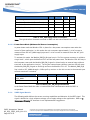
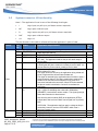
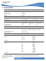
Many of the signals present in the interface are CMOS signals where the following levels apply.
The nominal voltage level for the CMOS signals is 2.9 V. Drive capability of the outputs is also
indicated.
Parameter
Test
Conditions
High level output voltage (IOH = 800 µA)
Low level output voltage (IOL = 800 µA)
High level input voltage
Low level input voltage
VOH
VOL
VIH
VIL
Limits
Min
2.45
0
1.9
0
Units
Max
3.1
0.45
3.1
0.9
Volts
Volts
Volts
Volts
Table 4: CMOS Output / Input Electrical Characteristics
Note: The maximum voltage that may be applied to any CMOS signal is 3.1V
2.3.3.1 Leakage Current for CMOS Signals
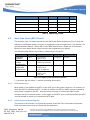
The following table defines the maximum leakage for the CMOS inputs of the CM52.
Parameter
High level drive for input signal with internal pull down
Low level drive for input signal with internal pull up
3
Max
Units
60
uA
60
uA
Table 5: Maximum Leakage Current for CMOS signals
2.3.3.2 Validity of CMOS signals
The CMOS signals of the CM52 shall only be considered valid when the level of the VREF signal is
above 2.3V.
2.4
Power Supply
The CM52 requires a dual DC power supply implementation in the application. VCC_MAIN provides
power to the entire radio while VCC_AUX provides power for the 3-Watt functionality and biasing
for the RF switches.
Note: VCC_AUX must be present if the 3W option is provided even if it is not used. If the 3W
circuitry is not populated then VCC_AUX is not required or may be bussed together with
VCC_MAIN.
3
DTR is 90 uA and HW_SD is 350 uA
CM52 Integrators’ Manual
WI_DEV_CM52_UGD_001-001
Page 21 of 53
This document is the sole and exclusive property of WAVECOM. Not to be distributed or divulged without prior written agreement.
Ce document est la propriété exclusive de WAVECOM. Il ne peut être communiqué ou divulgué à des tiers sans son autorisation préalable