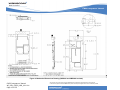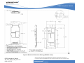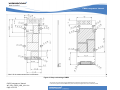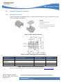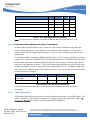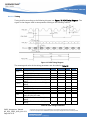
1
USER GUIDE CM52 Integrators’ Manual Reference: WI_DEV_CM52_UGD_001 Version: 001 Date: June 20, 2007 CM52 Integrators’ Manual Trademarks ®, WAVECOM®, WISMO®, Open AT®, Wireless CPU®, Wireless Microprocessor® and certain other trademarks and logos appearing on this document, are filed or registered trademarks of Wavecom S.A. in France or in other countries. All other company and/or product names mentioned may be filed or registered trademarks of their respective owners. Copyright This manual is copyrighted by WAVECOM with all rights reserved. No part of this manual may be reproduced in any form without the prior written permission of WAVECOM. No patent liability is assumed with respect to the use of the information contained herein. No Warranty This document is provided “as is” without any warranty of any kind. WAVECOM makes no warranties of any kind, either express or implied, including any implied warranties of merchantability, fitness for a particular purpose or noninfringement. CM52 Integrators’ Manual WI_DEV_CM52_UGD_001-001 Page 2 of 53 This document is the sole and exclusive property of WAVECOM. Not to be distributed or divulged without prior written agreement. Ce document est la propriété exclusive de WAVECOM. Il ne peut être communiqué ou divulgué à des tiers sans son autorisation préalable CM52 Integrators’ Manual Table of Contents 1 Introduction to the Integrator’s Manual ............................................................ 9 1.1 OVERVIEW ............................................................................................................................... 9 1.2 HOW TO READ THE MANUAL ................................................................................................... 9 1.3 SERVICE AND SUPPORT............................................................................................................ 9 1.3.1 WEB PAGES ......................................................................................................................... 9 1.4 RELATED DOCUMENTS .......................................................................................................... 10 1.5 ABBREVIATIONS..................................................................................................................... 10 2 Integrating the CM52 Wireless CPU® ............................................................... 11 2.1 OVERVIEW ............................................................................................................................. 11 2.2 MECHANICAL DESCRIPTION ................................................................................................... 11 2.2.1 2.2.2 2.2.3 2.2.3.1 2.2.3.2 2.2.4 MECHANICAL DIMENSIONS .......................................................................................... 11 HEAT-SINK REQUIREMENTS ......................................................................................... 16 MOUNTING HOLES ...................................................................................................... 16 MOUNTING CONFIGURATION A ................................................................................... 16 MOUNTING CONFIGURATION B.................................................................................... 17 RF CONNECTOR MOUNTING CONSIDERATIONS ............................................................ 17 2.3 SYSTEM CONNECTOR INTERFACE........................................................................................... 18 2.3.1 2.3.2 MECHANICAL OVERVIEW.............................................................................................. 18 SYSTEM CONNECTOR INTERFACE PINOUT .................................................................... 19 2.3.3 LOGIC LEVELS ............................................................................................................. 21 2.3.3.1 LEAKAGE CURRENT FOR CMOS SIGNALS ...................................................................... 21 2.3.3.2 VALIDITY OF CMOS SIGNALS ....................................................................................... 21 2.4 POWER SUPPLY ...................................................................................................................... 21 2.4.1 2.4.2 2.4.2.1 2.4.2.2 POWER SUPPLY INPUT CAPACITANCE ........................................................................... 22 POWER SUPPLY AND GROUND SIGNALS........................................................................ 23 POWER SUPPLY SIGNAL PINS ........................................................................................ 23 GROUND SIGNAL PINS ................................................................................................. 23 CM52 Integrators’ Manual WI_DEV_CM52_UGD_001-001 Page 3 of 53 This document is the sole and exclusive property of WAVECOM. Not to be distributed or divulged without prior written agreement. Ce document est la propriété exclusive de WAVECOM. Il ne peut être communiqué ou divulgué à des tiers sans son autorisation préalable CM52 Integrators’ Manual 2.4.3 2.4.3.1 2.4.3.2 2.4.3.3 2.4.4 POWER CONSUMPTION ................................................................................................ 23 VCC_MAIN SUPPLY POWER CONSUMPTION................................................................... 24 VCC_AUX SUPPLY POWER CONSUMPTION..................................................................... 24 POWER DOWN MODE (MINIMUM DC POWER CONSUMPTION) ........................................ 25 VREF SIGNAL DETAILS ................................................................................................. 25 2.5 REAL TIME CLOCK (RTC) CIRCUIT........................................................................................... 26 2.5.1 2.5.2 RTC INITIALIZATION.................................................................................................... 26 RTC FUNCTIONAL BLOCK DIAGRAM............................................................................. 26 2.6 AUDIO INTERFACE ................................................................................................................. 27 2.6.1 2.6.1.1 2.6.1.2 2.6.2 DIGITAL AUDIO ........................................................................................................... 28 DATA FORMAT............................................................................................................ 28 TIMING ....................................................................................................................... 29 ANALOG AUDIO .......................................................................................................... 30 2.7 SERIAL DATA INTERFACE ....................................................................................................... 33 2.8 ANTENNA INTERFACE ............................................................................................................ 33 2.8.1 ANTENNA CONNECTOR............................................................................................... 34 2.8.2 RF OUTPUT POWER...................................................................................................... 35 2.8.3 CARRIER APPROVAL .................................................................................................... 36 2.8.4 3 ANTENNA DIAGNOSTICS ............................................................................................. 36 Recommended Interface Circuitry................................................................... 38 3.1 STATUS GROUP RECOMMENDED CIRCUITRY........................................................................... 38 3.1.1 3.1.2 3.1.3 3.1.4 MODULE_PWR_EN_B .................................................................................................... 39 VREF ........................................................................................................................... 39 RI ............................................................................................................................... 40 HW_SD........................................................................................................................ 40 3.2 DATA GROUP RECOMMENDED CIRCUITRY.............................................................................. 42 3.2.1 VPPFLASH/DCD........................................................................................................... 42 3.3 PCM GROUP RECOMMENDED CIRCUITRY ................................................................................ 43 3.4 ANALOG AUDIO GROUP RECOMMENDED CIRCUITRY .............................................................. 44 3.4.1 3.4.2 3.4.3 CREATING AN ANALOG GROUND................................................................................. 44 ANALOG GROUND VS. AGND ....................................................................................... 45 MICROPHONE PATH .................................................................................................... 45 CM52 Integrators’ Manual WI_DEV_CM52_UGD_001-001 Page 4 of 53 This document is the sole and exclusive property of WAVECOM. Not to be distributed or divulged without prior written agreement. Ce document est la propriété exclusive de WAVECOM. Il ne peut être communiqué ou divulgué à des tiers sans son autorisation préalable CM52 Integrators’ Manual 3.4.4 LOUDSPEAKER PATH ................................................................................................... 46 3.5 SYSTEM CONNECTOR IO FUNCTIONALITY .............................................................................. 47 4 Functional Description ................................................................................... 49 5 Hints for Integrating the Wireless CPU® .......................................................... 50 5.1 PRECAUTIONS ....................................................................................................................... 50 5.2 WHERE TO INSTALL THE WIRELESS CPU® ................................................................................. 50 5.3 SAFETY STANDARDS.............................................................................................................. 50 5.4 ANTENNA.............................................................................................................................. 51 5.4.1 5.4.2 ANTENNA TYPE ........................................................................................................... 51 ANTENNA PLACEMENT ................................................................................................ 51 5.5 POSSIBLE COMMUNICATION DISTURBANCES .......................................................................... 51 6 Technical Data ............................................................................................... 52 CM52 Integrators’ Manual WI_DEV_CM52_UGD_001-001 Page 5 of 53 This document is the sole and exclusive property of WAVECOM. Not to be distributed or divulged without prior written agreement. Ce document est la propriété exclusive de WAVECOM. Il ne peut être communiqué ou divulgué à des tiers sans son autorisation préalable CM52 Integrators’ Manual List of Tables TABLE 1: ABBREVIATION DEFINITIONS ................................................................................................ TABLE 2: SYSTEM CONNECTOR AND MATING PART NUMBERS ..................................................................... TABLE 3: PIN-OUT OF THE SYSTEM CONNECTOR HEADER........................................................................... TABLE 4: CMOS OUTPUT / INPUT ELECTRICAL CHARACTERISTICS .............................................................. TABLE 5: MAXIMUM LEAKAGE CURRENT FOR CMOS SIGNALS ..................................................................... TABLE 6: CM52 POWER SUPPLY REQUIREMENTS .................................................................................... TABLE 7: POWER SUPPLY INPUT CAPACITANCE (0.6W VARIANTS) ............................................................. TABLE 8: POWER SUPPLY INPUT CAPACITANCE (3W VARIANTS) ................................................................ TABLE 9: CM52 POWER SUPPLY SIGNALS ............................................................................................. TABLE 10: CM52 GROUND SIGNALS .................................................................................................... TABLE 11: VCC_MAIN SUPPLY POWER CONSUMPTION ........................................................................... TABLE 12: VCC_AUX SUPPLY POWER CONSUMPTION ............................................................................. TABLE 13: MODULE_PWR_EN_B SIGNAL PARAMETERS ........................................................................... TABLE 14: VREF SUPPLY DETAILS ...................................................................................................... TABLE 15: FREQUENCY CHARACTERISTICS OF THE RTC............................................................................. TABLE 16: CM52 AUDIO SIGNALS ...................................................................................................... TABLE 17: CM52 DIGITAL AUDIO SIGNALS .......................................................................................... TABLE 18: PCM TIMING PARAMETERS ................................................................................................. TABLE 19: CM52 ANALOG AUDIO SIGNALS ........................................................................................... TABLE 20: AUDIO CHARACTERISTICS ................................................................................................... TABLE 21: SERIAL DATA CHANNELS..................................................................................................... TABLE 22: ANTENNA CONNECTOR SUPPLIERS ........................................................................................ TABLE 23: MOBILE STATION NOMINAL ANALOG POWER LEVELS ................................................................. TABLE 24: MOBILE STATION CDMA MAXIMUM OUTPUT POWER ................................................................. TABLE 25: RANGE OF ADC READINGS FOR AN EXTERNAL ANTENNA .............................................................. TABLE 26: PIN DIRECTION FOR GENERAL PURPOSE SIGNALS ..................................................................... TABLE 27: TECHNICAL DATA .............................................................................................................. CM52 Integrators’ Manual WI_DEV_CM52_UGD_001-001 Page 6 of 53 This document is the sole and exclusive property of WAVECOM. Not to be distributed or divulged without prior written agreement. Ce document est la propriété exclusive de WAVECOM. Il ne peut être communiqué ou divulgué à des tiers sans son autorisation préalable 10 18 20 21 21 22 22 22 23 23 24 25 25 26 26 27 28 29 30 30 33 35 36 36 37 48 53 CM52 Integrators’ Manual List of Figures FIGURE 1: CM52 PRIMARY SIDE ........................................................................................................ FIGURE 2: CM52 SECONDARY SIDE ..................................................................................................... FIGURE 3: MECHANICAL DIMENSIONS DRAWING (CM52003 VARIANT) ...................................................... FIGURE 4: MECHANICAL DIMENSIONS DRAWING (CM52001 AND CM52004 VARIANTS)................................ FIGURE 5: MECHANICAL DIMENSIONS DRAWING (CM52002 VARIANT) ...................................................... FIGURE 6: KEEP-OUT DRAWING OF CM52 ............................................................................................. FIGURE 7: MOUNTING CONFIGURATION A ............................................................................................. FIGURE 8: MOUNTING CONFIGURATION B ............................................................................................. FIGURE 9: APPLICATION HOUSING ...................................................................................................... FIGURE 10: 40-PIN SYSTEM CONNECTOR ............................................................................................. FIGURE 11: 40-PIN SYSTEM CONNECTOR PIN NUMBERING ....................................................................... FIGURE 12: RTC FUNCTIONAL BLOCK DIAGRAM ..................................................................................... FIGURE 13: PCM TIMING DIAGRAM .................................................................................................... FIGURE 14: BIAS DIAGRAM EXAMPLE ................................................................................................. FIGURE 15: MICROPHONE IMPLEMENTATION EXAMPLE ............................................................................. FIGURE 16: DIFFERENTIAL IMPLEMENTATION EXAMPLE ............................................................................ FIGURE 17: COLOR AND KEYING FOR VARIOUS FAKRA CONNECTORS .......................................................... FIGURE 18: SAMPLE SMA CONNECTOR AND MOUNTING HOLE .................................................................... FIGURE 19: ANTENNA DIAGNOSTIC CIRCUIT ......................................................................................... FIGURE 20: STATUS GROUP DIAGRAM .................................................................................................. FIGURE 21: PIN 15 HW_SD DIAGRAM................................................................................................ FIGURE 22: SHUT DOWN SEQUENCE TIMELINE ....................................................................................... FIGURE 23: DATA GROUP DIAGRAM .................................................................................................... FIGURE 24: PCM GROUP DIAGRAM ..................................................................................................... FIGURE 25: CREATING AN ANALOG REFERENCE VOLTAGE (BIAS)................................................................ FIGURE 26: BIAS/VANA REFERENCE ................................................................................................. FIGURE 27: MICROPHONE IMPLEMENTATION EXAMPLE ............................................................................. FIGURE 28: LOUDSPEAKER IMPLEMENTATION EXAMPLE ............................................................................ CM52 Integrators’ Manual WI_DEV_CM52_UGD_001-001 Page 7 of 53 This document is the sole and exclusive property of WAVECOM. Not to be distributed or divulged without prior written agreement. Ce document est la propriété exclusive de WAVECOM. Il ne peut être communiqué ou divulgué à des tiers sans son autorisation préalable 11 11 12 13 14 15 16 17 17 18 18 27 29 31 32 32 34 35 37 39 40 41 42 43 44 44 45 46 CM52 Integrators’ Manual Revision History Release Date Summary of Changes PA1 PA2 PA3 PA4 PA5 PA6 05/07/2004 09/01/2004 11/17/2004 11/29/2004 12/01/2004 06/16/2005 A PB1 09/15/2005 11/30/2005 PB2 PB3 02/16/2006 03/08/2006 PB4 03/16/2006 PB5 03/22/2006 B PC1 PC2 03/24/2006 06/02/2006 06/13/2006 001 06/20/2007 Initial Draft Formatting Updated Chapters 1 & 2 Updated with review feedback Updated the List of Tables and Figures Current Consumption Table, RTC Block Diagram, Mechanical Drawing Release version Updates for VREF sourcing capability, inrush current, mechanical mounting, recommended application circuitry and CMOS leakage current. Update to Power consumption section & Formatting updates Updated mechanical drawings, Re-formatted Table 2, Added RTC Frequency Characteristics. Updated Sections: 2.5 - Real Time Clock Circuit, 2.8.2 – RF Output Power. Added section 3.1.3 – RI Updated Table of Contents. Updated Sections: 3.1.3 – RI and 3.1.4 – HW_SD. Removed the Random Stationary Vibration information from Section 6 – Technical Data. Release Version Updated Vibration Specification and add Minimum Off-Time Added RTC Initialization section and reformatted Technical Data table Update product references, Wavecom format CM52 Integrators’ Manual WI_DEV_CM52_UGD_001-001 Page 8 of 53 This document is the sole and exclusive property of WAVECOM. Not to be distributed or divulged without prior written agreement. Ce document est la propriété exclusive de WAVECOM. Il ne peut être communiqué ou divulgué à des tiers sans son autorisation préalable CM52 Integrators’ Manual 1 Introduction to the Integrator’s Manual 1.1 Overview This manual is for use as a guide to the setup, installation, and use of the CM52 Wireless CPU® into your application. The Wireless CPU® may be tested using the developer’s board, which is supplied together with all the necessary tools in the Developer’s Kit. 1.2 How to Read the Manual This manual is divided into six chapters: Chapter 1 gives a general view of the integrator’s manual. A list of related documents as well as a list of abbreviations used throughout the manual is also included. Information concerning service and support is also presented. Chapter 2 focuses on helping the hardware developer to integrate the CM52 hardware into their application. An overview of the mechanical and electrical information is provided. Interface specifications, RF output power, and power supply issues are included in this chapter. Chapter 3 contains information on recommended circuitry needed to ensure proper performance from the CM52 Wireless CPU®. Chapter 4 describes several of the common cellular functions available with the CM52. Chapter 5 provides some hints for integrating the Wireless CPU®. Chapter 6 provides a summary of the technical data for the CM52 Wireless CPU®. 1.3 Service and Support 1.3.1 Web Pages Visit our Web site for more information about where you can buy our products or for recommendations for accessories and components. The address is: http://www.wavecom.com To register for product news and announcements or for product questions, work with your usual Wavecom contact. CM52 Integrators’ Manual WI_DEV_CM52_UGD_001-001 Page 9 of 53 This document is the sole and exclusive property of WAVECOM. Not to be distributed or divulged without prior written agreement. Ce document est la propriété exclusive de WAVECOM. Il ne peut être communiqué ou divulgué à des tiers sans son autorisation préalable CM52 Integrators’ Manual 1.4 Related Documents CM52 AT Command Manual – Details the AT command interface for the CM52 The CM52 is based upon the following mobile standards: IS-2000 Release 0 (1XRTT), MOB_P_REV – CDMA protocol TIA/EIA/IS-91 – Mobile Station – Base Station Compatibility Standard for 800 MHz Analog Cellular TIA/EIA-98-D – Recommended Minimum Performance Standards for Dual-Mode Spread Spectrum Mobile Stations 1.5 Abbreviations Abbreviation AGND AMPS AT CDMA CTS DCD DFMS DTMS DTR EMI ESD GND IRA LSB ME MO MS MT OEM PCB PCM PIN PSD RD RF RI RTS SMS TD Definition Analog Reference Advanced Mobile Phone System Attention Command Code Division Multiple Access Clear to Send Data Carrier Detect Data from Mobile Station Data to Mobile Station Data Terminal Ready Electromagnetic Interference Electrostatic Discharge Chassis GrouND International Reference Alphabet Least Significant Bit Mobile Equipment Mobile Originated Mobile Station Mobile Terminated Original Equipment Manufacturer Printed Circuit Board Pulse Code Modulation Personal Identification Number Power Spectral Density Receive Data, also known as DFMS Radio Frequency Ring Indicator Request to Send Short Message Service Transmit Data, also know as DTMS Table 1: Abbreviation Definitions CM52 Integrators’ Manual WI_DEV_CM52_UGD_001-001 Page 10 of 53 This document is the sole and exclusive property of WAVECOM. Not to be distributed or divulged without prior written agreement. Ce document est la propriété exclusive de WAVECOM. Il ne peut être communiqué ou divulgué à des tiers sans son autorisation préalable CM52 Integrators’ Manual 2 Integrating the CM52 Wireless CPU® 2.1 Overview The CM52 is a dual band, dual mode CDMA transceiver Wireless CPU®. It operates in the 800 MHz band for CDMA and AMPS and in the 1900 MHz band for CDMA. It is designed for consumer and OEM industrial voice and data applications. The CM52 Wireless CPU® is intended for mounting into an application developer’s chassis to provide wireless communication capability for the product. The target chassis could be in a wide variety of forms such as a residential electric meter, a point of sale terminal, an alarm panel, or an automobile console. All initial configuration, mode control, and operational commands are issued to the Wireless CPU® over an RS-232 serial port using a flexible AT command format. The Wireless CPU® circuitry has been designed to meet the environmental requirements of a large range of commercial and industrial users. 2.2 Mechanical Description The CM52 has no mechanical elements other than the main PCB assembly. All critical electronic components are shielded using six cans to prevent internal and external electromagnetic interference from degrading the Wireless CPU performance and to prevent the Wireless CPU® from interfering with other nearby devices. The Wireless CPU® is plugged into the fixed mating connector and secured with four screws. The antenna interface is provided via a board mounted RF connector at the opposite end of the board from the system connector. See Section 2.8 for more information on antenna connector options. The Wireless CPU® has no keypad, display, microphone, speaker, or battery. The following figures show 3-D models of the Wireless CPU®. Figure 1: CM52 Primary Side 2.2.1 Figure 2: CM52 Secondary Side Mechanical Dimensions The following figures provide the mechanical dimensions for several CM52 variants (CM52002, CM52003, and CM52004). There is also a drawing detailing the mechanical keep-out regions. CM52 Integrators’ Manual WI_DEV_CM52_UGD_001-001 Page 11 of 53 This document is the sole and exclusive property of WAVECOM. Not to be distributed or divulged without prior written agreement. Ce document est la propriété exclusive de WAVECOM. Il ne peut être communiqué ou divulgué à des tiers sans son autorisation préalable CM52 Integrators’ Manual Note! All the measurements are in millimeters. Figure 3: Mechanical Dimensions Drawing (CM52003 variant) CM52 Integrators’ Manual WI_DEV_CM52_UGD_001-001 Page 12 of 53 This document is the sole and exclusive property of WAVECOM. Not to be distributed or divulged without prior written agreement. Ce document est la propriété exclusive de WAVECOM. Il ne peut être communiqué ou divulgué à des tiers sans son autorisation préalable CM52 Integrators’ Manual Note! All the measurements are in millimeters. Figure 4: Mechanical Dimensions Drawing (CM52001 and CM52004 variants) CM52 Integrators’ Manual WI_DEV_CM52_UGD_001-001 Page 13 of 53 This document is the sole and exclusive property of WAVECOM. Not to be distributed or divulged without prior written agreement. Ce document est la propriété exclusive de WAVECOM. Il ne peut être communiqué ou divulgué à des tiers sans son autorisation préalable CM52 Integrators’ Manual Note! All the measurements are in millimeters. Figure 5: Mechanical Dimensions Drawing (CM52002 variant) CM52 Integrators’ Manual WI_DEV_CM52_UGD_001-001 Page 14 of 53 This document is the sole and exclusive property of WAVECOM. Not to be distributed or divulged without prior written agreement. Ce document est la propriété exclusive de WAVECOM. Il ne peut être communiqué ou divulgué à des tiers sans son autorisation préalable CM52 Integrators’ Manual Note! All the measurements are in millimeters. Figure 6: Keep-out drawing of CM52 CM52 Integrators’ Manual WI_DEV_CM52_UGD_001-001 Page 15 of 53 This document is the sole and exclusive property of WAVECOM. Not to be distributed or divulged without prior written agreement. Ce document est la propriété exclusive de WAVECOM. Il ne peut être communiqué ou divulgué à des tiers sans son autorisation préalable CM52 Integrators’ Manual 2.2.2 Heat-Sink Requirements The application is required to provide a heat-sink for the 3W AMPS capabilities of the CM52. The application should be designed to provide a heat sink with a thermal resistance of 4.0 °C/W. For applications that disable the 3W mode (Class I) and only operate in 0.6W mode (Class III) a heat-sink is not required. 2.2.3 Mounting Holes Mounting holes and tabs are provided for proper mechanical support of the CM52 Wireless CPU® in the customer’s application. The OEM’s application must provide sufficient mechanical retention using the mounting holes and/or tabs or some other means. The system connector and RF connector connections should not be used as a means of mechanical support. Also, please note that the mounting holes may not substitute for the actual grounding pins provided via the system connector. Two mounting configurations are supported (A and B). Each has its own mechanical vibration specification. Section 6 details the mechanical vibration specification for both configurations. For machine screw mounting a wet torque of 8 in-lbs is recommended. 2.2.3.1 Mounting Configuration A Mounting configuration “A” uses four exterior mounting holes that support #4 size screws. Figure 7: Mounting Configuration A CM52 Integrators’ Manual WI_DEV_CM52_UGD_001-001 Page 16 of 53 This document is the sole and exclusive property of WAVECOM. Not to be distributed or divulged without prior written agreement. Ce document est la propriété exclusive de WAVECOM. Il ne peut être communiqué ou divulgué à des tiers sans son autorisation préalable CM52 Integrators’ Manual 2.2.3.2 Mounting Configuration B Mounting configuration “B” uses four 3/4 mounting holes that support #6 size screws. Figure 8: Mounting Configuration B Note: This is the recommend mounting configuration due to the higher mechanical vibration specification supported. 2.2.4 RF Connector Mounting Considerations When designing the application the designer should ensure that the housing does not degrade the RF performance of the CM52. A minimum clearance of 4mm from the surface of the PCB to the housing on the back side of the RF connectors should be provided. 4mm Figure 9: Application Housing CM52 Integrators’ Manual WI_DEV_CM52_UGD_001-001 Page 17 of 53 This document is the sole and exclusive property of WAVECOM. Not to be distributed or divulged without prior written agreement. Ce document est la propriété exclusive de WAVECOM. Il ne peut être communiqué ou divulgué à des tiers sans son autorisation préalable CM52 Integrators’ Manual 2.3 System Connector Interface 2.3.1 Mechanical Overview External interfaces to the Wireless CPU® are made primarily through a 40 pin, standard 0.050-inch pitch, ODU header show below. Figure 10: 40-Pin System Connector Figure 11: 40-Pin System Connector Pin Numbering Description ODU Part Number Dimension A Dimension B System Connector Mating Ribbon Connector SMT Mating Header Ribbon cable, AWG 30 515.569.035.140.xxx 525.060.035.040.xxx 24.13 mm 22.86 mm 525.041.035.040.xxx 921.659.031.040.000 Table 2: System Connector and Mating Part Numbers Please consult the ODU site for more information on mating options: http://www.odu.de CM52 Integrators’ Manual WI_DEV_CM52_UGD_001-001 Page 18 of 53 This document is the sole and exclusive property of WAVECOM. Not to be distributed or divulged without prior written agreement. Ce document est la propriété exclusive de WAVECOM. Il ne peut être communiqué ou divulgué à des tiers sans son autorisation préalable CM52 Integrators’ Manual 2.3.2 1 2 System Connector Interface Pinout Pin Signal 1 2 3 4 5 6 7 8 9 10 11 12 Reserved VREF Reserved VRTC GND GND AFMS GND AGND ATMS Reserved MODULE_PWR_EN_B 13 14 15 16 17 18 19 20 21 22 23 Reserved Reserved HW_SD Reserved PCMCLK PCMSYNC PCMULD PCMDLD GND GND DCD / VPPFLASH 24 Reserved Description Dir Pin Type Alternate Function Dir Pin Type O CMOS GPS Fix 1 GPS VRTC1 O I CMOS Supply UART3_RX1 I CMOS UART3_TX1 O CMOS RINGER O CMOS TIMEMARK Logic Voltage O Supply pin for RTC 2 Chassis Ground Chassis Ground Analog Audio from Wireless CPU® Chassis Ground Analog Reference Analog Audio to Wireless CPU® ® Switches the Wireless CPU on/off (hardware-wise), active low I O I 1 Reference Power Ground Ground Audio Ground Audio Audio I Hardware shutdown I/O PCM Clock output PCM Frame sync PCM Voice input to Wireless CPU® PCM Voice output from Wireless CPU® Chassis Ground Chassis Ground Data Carrier Detect & Flash programming voltage input O O I O O/I O CMOS CMOS CMOS CMOS Ground Ground CMOS / Power Default function if GPS option on board Default function if RTC option on board CM52 Integrators’ Manual WI_DEV_CM52_UGD_001-001 Page 19 of 53 This document is the sole and exclusive property of WAVECOM. Not to be distributed or divulged without prior written agreement. Ce document est la propriété exclusive de WAVECOM. Il ne peut être communiqué ou divulgué à des tiers sans son autorisation préalable CM52 Integrators’ Manual Pin Signal Description Dir Pin Type 25 26 27 28 29 30 31 32 33 34 35 36 37 38 39 40 CTS DTR TD RTS VCC_AUX RD VCC_AUX VCC_AUX VCC_MAIN VCC_MAIN SDA_SPI_IN SCL_SPI_CLK SYS_DTM_2 SPI_OUT SYS_DFM_2 RI Clear to send Data Terminal Ready Transmit data, also known as DTMS Request to Send 13.8 VDC supply input Receive data, also known as DFMS 13.8 VDC supply input 13.8 VDC supply input 5 VDC regulated supply 5 VDC regulated supply Reserved Reserved Transmit Data for UART2 Reserved Receive Data for UART2 Ring Indicator O I I I I O I I I I CMOS CMOS CMOS CMOS Power CMOS Power Power Power Power CMOS CMOS CMOS CMOS CMOS CMOS I O O Alternate Function Dir SDA_SPI_IN SCL_SPI_CLK GPS TX Data1 SPI_OUT GPS RX Data1 IO IO I IO O Table 3: Pin-out of the System Connector Header CM52 Integrators’ Manual WI_DEV_CM52_UGD_001-001 Page 20 of 53 This document is the sole and exclusive property of WAVECOM. Not to be distributed or divulged without prior written agreement. Ce document est la propriété exclusive de WAVECOM. Il ne peut être communiqué ou divulgué à des tiers sans son autorisation préalable Pin Type CM52 Integrators’ Manual 2.3.3 Logic Levels Many of the signals present in the interface are CMOS signals where the following levels apply. The nominal voltage level for the CMOS signals is 2.9 V. Drive capability of the outputs is also indicated. Parameter Test Conditions High level output voltage (IOH = 800 µA) Low level output voltage (IOL = 800 µA) High level input voltage Low level input voltage VOH VOL VIH VIL Limits Min 2.45 0 1.9 0 Units Max 3.1 0.45 3.1 0.9 Volts Volts Volts Volts Table 4: CMOS Output / Input Electrical Characteristics Note: The maximum voltage that may be applied to any CMOS signal is 3.1V 2.3.3.1 Leakage Current for CMOS Signals The following table defines the maximum leakage for the CMOS inputs of the CM52. Parameter High level drive for input signal with internal pull down Low level drive for input signal with internal pull up 3 Max Units 60 uA 60 uA Table 5: Maximum Leakage Current for CMOS signals 2.3.3.2 Validity of CMOS signals The CMOS signals of the CM52 shall only be considered valid when the level of the VREF signal is above 2.3V. 2.4 Power Supply The CM52 requires a dual DC power supply implementation in the application. VCC_MAIN provides power to the entire radio while VCC_AUX provides power for the 3-Watt functionality and biasing for the RF switches. Note: VCC_AUX must be present if the 3W option is provided even if it is not used. If the 3W circuitry is not populated then VCC_AUX is not required or may be bussed together with VCC_MAIN. 3 DTR is 90 uA and HW_SD is 350 uA CM52 Integrators’ Manual WI_DEV_CM52_UGD_001-001 Page 21 of 53 This document is the sole and exclusive property of WAVECOM. Not to be distributed or divulged without prior written agreement. Ce document est la propriété exclusive de WAVECOM. Il ne peut être communiqué ou divulgué à des tiers sans son autorisation préalable CM52 Integrators’ Manual The following table summarizes the power supply requirements from the application. Input Supply VCC_MAIN VCC_AUX VRTC(no GPS) VRTC(with GPS) Voltage (Volts DC) 5.00 ± 10% 13.8 ± 20% 1.8 to 3.9 3.4 to 3.9 Max. Current (Amps) Max. Ripple (mVpp) Operation 0- 4KHz 1.4 1.3 1.2 uA 500 uA 100mVpp 600mVpp 4 KHz10MHz 50mVpp 240mVpp Table 6: CM52 Power Supply Requirements 2.4.1 Power Supply Input Capacitance It should be noted that when applying power to the Wireless CPU®, the current will exceed the maximum input current specified in Table 6: CM52 Power Supply Requirements, or any other CM52 electrical specification due to the transient current required to charge the de-coupling capacitors of the Wireless CPU® (specified below as CIN). The magnitude and duration of the transient current spike is solely dependent on the application power supply design. Any built-in short circuit protection in the application power supply must take this in to account as well as all other "Power Supply" specifications. The maximum total input capacitance on VCC_MAIN is 100uF. However at “Contact”, 60uF will be charged instantly by the application’s power supply. Then at “Wake” an additional 14.5uF will be instantly charged. At that point internal regulators are activated and limit the charge rate of the remaining capacitance. If VCC_MAIN and VCC_AUX are tied together (0.6W variants only) then the input capacitance on VCC_AUX is negligible. The “Wakeup” condition occurs when the MODULE_PWR_EN_B signal transitions from High to Low. The “Contact” condition occurs when voltage is first asserted to VCC_MAIN, and or VCC_AUX. Parameter Contact Wakeup Units VCC_MAIN Input Capacitance (CIN) 60 14.5 uF VCC_AUX Input Capacitance (CIN) 33 10 pF Table 7: Power Supply Input Capacitance (0.6W variants) Parameter Contact Wakeup 3W assertion VCC_MAIN Input Capacitance (CIN) 60 uF 14.5 uF n/a VCC_AUX Input Capacitance (CIN) 10 uF 10 pF 20 uF Table 8: Power Supply Input Capacitance (3W variants) CM52 Integrators’ Manual WI_DEV_CM52_UGD_001-001 Page 22 of 53 This document is the sole and exclusive property of WAVECOM. Not to be distributed or divulged without prior written agreement. Ce document est la propriété exclusive de WAVECOM. Il ne peut être communiqué ou divulgué à des tiers sans son autorisation préalable CM52 Integrators’ Manual 2.4.2 Power Supply and Ground Signals 2.4.2.1 Power Supply Signal Pins Following is a list of the power supply pins: Pin Signal Description 4 4 VRTC 1.8 V to 3.9V ( 3.4V to 3.9V if GPS mounted) 29 VCC_AUX 13.8 volt ± 20% 31 32 33 34 VCC_AUX VCC_AUX VCC_MAIN VCC_MAIN 13.8 volt ± 20% 13.8 volt ± 20% 5 volt ± 10% regulated 5 volt ± 10% regulated Table 9: CM52 Power Supply Signals For the power supply signals in the above table with multiple pins defined, the application shall bus all defined pins together. 2.4.2.2 Ground Signal Pins The ground signal in the CM52 is Digital Ground, GND, connected to the system connector interface through pin numbers 5, 6, 8, 21 and 22. Following is a list of the ground pins: Pin Signal Description 5 6 8 21 22 GND GND GND GND GND Digital Ground Digital Ground Digital Ground Digital Ground Digital Ground Table 10: CM52 Ground Signals Digital Ground (GND) is the logical reference of all digital signals in the System Interface as well as the DC return of the power supply signal, VCC_MAIN and VCC_AUX (used for AMPS Class I operation). All 5 ground pins in the Wireless CPU® need to be connected to the application ground. The PCB mounting holes may not to be used as substitute for the ground signal pins of the system connector interface. 2.4.3 Power Consumption The following tables show typical and maximum values of current that can be expected from the Wireless CPU® in different modes of operation. 4 Only applicable to units with GPS or RTC functions CM52 Integrators’ Manual WI_DEV_CM52_UGD_001-001 Page 23 of 53 This document is the sole and exclusive property of WAVECOM. Not to be distributed or divulged without prior written agreement. Ce document est la propriété exclusive de WAVECOM. Il ne peut être communiqué ou divulgué à des tiers sans son autorisation préalable CM52 Integrators’ Manual 2.4.3.1 VCC_MAIN Supply Power Consumption Parameter Min Typical Max Units Input Voltage 4.5 5 5.5 V In AMPS Call on Power Level 0 (Power Class I) In AMPS Call on Power Level 2 0.62 0.82 A 0.94 1.4 A In CDMA call-Cellular Mode 0.77 1.2 A In CDMA call-PCS Mode 0.84 1.3 A CDMA burst duration for Network update 1.2 s Standby/Idle Current Draw in Slotted Mode (CDMA) 1.28 sec slot 9.6 mA 2.56 sec slot 7.2 mA 5.12 sec slot 4.5 mA Stand-by/Idle mode (AMPS) 45 mA Powered Down Current Draw 1 5 uA Table 11: VCC_MAIN Supply Power Consumption Notes 1. The typical current measurements noted in CDMA mode are with the following settings: a. CDMA-Cellular (800MHz): Band = IS-2000, Cell-Power = -104dBm, Channel Number 358 b. CDMA-PCS (1900MHz): Band = IS-2000, Cell-Power = -104dBm, Channel Number 563 Maximum Slot Cycle Index for both 800MHz and 1900MHz modes = 1 2. Measurements are based on worst case scenario—CM52 with 3W option. Values for CM52 with no 3W option could be marginally lower. 3. A +10% tolerance is allowed for the listed maximum values. 2.4.3.2 VCC_AUX Supply Power Consumption The VCC_AUX power supply is required for CM52 variants with 3W AMPS circuitry populated. This requirement is regardless of whether the AMPS Power Class 1 is used. The VCC_AUX power supply is not required for any CM52 Wireless CPU® other than those with 3W AMPS circuitry populated, but it can be applied if desired. In this case, the VCC_AUX pins can be supplied as 5V, 13.8V or Grounded. CM52 Integrators’ Manual WI_DEV_CM52_UGD_001-001 Page 24 of 53 This document is the sole and exclusive property of WAVECOM. Not to be distributed or divulged without prior written agreement. Ce document est la propriété exclusive de WAVECOM. Il ne peut être communiqué ou divulgué à des tiers sans son autorisation préalable CM52 Integrators’ Manual Parameter Min Typical Max Units Input Voltage 11 13.8 16.6 V In a Call on Power Level 0 (Power Class I) 0.88 1.3 A In a Call on Power Level 2 3.5 4.5 mA AMPS Burst Duration for network update 0.16 Stand-by/Idle mode (Rx ON) 0.5 Powered Down Current Draw 1 S 1 uA uA Table 12: VCC_AUX Supply Power Consumption Note: The typical values observed are made in AMPS call with voice channel set to 358. 2.4.3.3 Power Down Mode (Minimum DC Power Consumption) In power down mode the Wireless CPU® is placed in a low power consumption state under the control of host application. In this mode, the unit consumes approximately 1 uA of current as measured from the VCC_MAIN supply input and 1 uA of current as measured from the VCC_AUX supply input. To activate this mode, the Module_PWR_EN_B signal on pin 12 of the system connector is pulled to a logic level 1, which puts the Wireless CPU® into the low power state. The Wireless CPU® will stay in the low power state until the Module_PWR_EN_B signal is driven low by an external open collector transistor in the application circuitry. Turning the external open collector transistor off will cause the Module_PWR_EN_B signal to float high and turn the Wireless CPU® off. The Module_PWR_EN_B line is tied to VCC_MAIN through a 100kΩ pull-up resistor so the sink current in the external open collector transistor is minimal. Parameter Minimum Nominal Internal Pull-up Resistance to VCC_MAIN Off-Time 90 100 Maximum 1 Units KΩ S Table 13: Module_Pwr_EN_B Signal Parameters In the Power Down Mode the radio is inactive and serial communication with the CM52 is suspended. 2.4.4 VREF Signal Details The following table defines the current sourcing capabilities and behavior of the VREF signal. This signal is defined as a logic reference voltage, not a supply voltage to the application. Refer to 3 Recommend Circuitry for interface circuit implementation suggestions. CM52 Integrators’ Manual WI_DEV_CM52_UGD_001-001 Page 25 of 53 This document is the sole and exclusive property of WAVECOM. Not to be distributed or divulged without prior written agreement. Ce document est la propriété exclusive de WAVECOM. Il ne peut être communiqué ou divulgué à des tiers sans son autorisation préalable CM52 Integrators’ Manual Parameter Minimum Typical Maximum Units Supply Voltage Reference 2.45 2.9 3.1 V 1000 uA Output Current Application Load 10 100 KΩ Rise Time 3300 us Fall Time 0.8 ms Table 14: VREF Supply Details 2.5 Real Time Clock (RTC) Circuit The real time clock is a feature provided by the CM52 that allows the Wireless CPU® to sleep and wakeup for a definable number of cycles, as configured by the host application. This feature is an optional hardware feature. Please refer to the CM52 Software User’s Guide and AT Command Manual for more details about usage scenarios and programming this feature. The following table defines the Frequency Characteristics of the RTC: Item Symbol Condition Rating Unit Frequency precision Frequency / voltage characteristics Frequency / temperature characteristics Aging Δf / f Ta = +25 °C, VDD = 3.0 V Ta = +25 °C, VDD = 2.0 V to 5.0 V 5 ± 23 (*1) X 10-6 ± 2 Max. X 10 -6 / V +10 / -120 X 10 -6 ± 5 Max. X 10 -6 / year f/V Top fa Ta = -20 °C to +70 °C, VDD = 3.0 V; +25 °C reference Ta = +25 °C, VDD = 3.0V, first year Table 15: Frequency characteristics of the RTC (*1) precision gap per month: 1 minutes (excluding offset value) 2.5.1 RTC Initialization When power is first applied to the RTC via the VRTC pin of the system connector it is necessary to allow the CM52 to initialize the RTC. In order to initialize the RTC the CM52 must be powered up while power is applied to the RTC. Once the Restart message is received the CM52 can be shutdown via the normal procedures. If the supply to the VRTC input is interrupted then the CM52 must be allowed to power up to initialize the RTC again. 2.5.2 RTC Functional Block Diagram The purpose of this section is to provide an overview of the Real Time Clock feature functional block and interconnects that are shared with the application. CM52 Integrators’ Manual WI_DEV_CM52_UGD_001-001 Page 26 of 53 This document is the sole and exclusive property of WAVECOM. Not to be distributed or divulged without prior written agreement. Ce document est la propriété exclusive de WAVECOM. Il ne peut être communiqué ou divulgué à des tiers sans son autorisation préalable CM52 Integrators’ Manual Figure 12: RTC Functional Block Diagram 2.6 Audio Interface The audio-related signals are: the analog audio signals ATMS (Audio to Mobile Station), AFMS (Audio from Mobile Station), PCM (Pulse Code Modulation) signals (PCMULD, PCMDLD, PCMCLK, and PCMSYNC). Pin Signal Description 7 AFMS Audio Output From Wireless CPU®. 10 ATMS Audio Input to Wireless CPU®. 9 AGND Analog Reference 17 PCMCLK PCM Clock Output from Wireless CPU®. 18 PCMSYNC PCM Frame Sync Output from Wireless CPU®. 19 PCMULD PCM Voice Input to Wireless CPU® 20 PCMDLD PCM Voice Output from Wireless CPU®. Table 16: CM52 Audio Signals CM52 Integrators’ Manual WI_DEV_CM52_UGD_001-001 Page 27 of 53 This document is the sole and exclusive property of WAVECOM. Not to be distributed or divulged without prior written agreement. Ce document est la propriété exclusive de WAVECOM. Il ne peut être communiqué ou divulgué à des tiers sans son autorisation préalable CM52 Integrators’ Manual 2.6.1 Digital Audio The CM52 provides digital audio capability over the system connector. The digital audio signals enable the connection of a digital audio source. The receiver is bypassing the analog audio processing functions performed within the Wireless CPU®. The digital audio interface includes the following PCM signals: Pin Signal Description 17 PCMCLK PCM Clock Output from Wireless CPU®. 18 PCMSYNC PCM Frame Sync from Wireless CPU® 19 PCMULD PCM Voice Input to Wireless CPU®. 20 PCMDLD PCM Voice Output from Wireless CPU®. Table 17: CM52 Digital Audio Signals Already defined CMOS output/input electrical characteristics apply (see Section 1.1.1). The PCM signals are referenced to digital ground. The PCM format (for PCMULD and PCMDLD) follows a linear PCM data format with 13-bit data embedded in a 16-bit word. The data bits in PCMULD (input) and PCMDLD (output) are aligned so that the MSB in each word occurs on the same clock edge. See timing diagram in 2.6.1.2. 2.6.1.1 Data Format The CM52 Wireless CPU® implements a 13-bit linear PCM with the 13-bit data embedded in a 16bit word as follows. Each PCM word shall contain 16-bits D15 – D00. D15 – D03 is the 2´s-complement value of the 13-bit PCM, with D15 as the sign bit. D15 is the MSB while D03 is the LSB. Note that the MSB is sent in first place. Ensure that the read data from PCMDLD is right shifted three times and sign extended before being used 15 14 13 12 11 10 9 13-bit linear 8 7 6 MSB 4 3 LSB Bit Contents D15 – D03 D02 – D00 2’s complement of the 13-bit PCM. Bits are undefined. CM52 Integrators’ Manual WI_DEV_CM52_UGD_001-001 Page 28 of 53 5 2 x 1 x 0 x This document is the sole and exclusive property of WAVECOM. Not to be distributed or divulged without prior written agreement. Ce document est la propriété exclusive de WAVECOM. Il ne peut être communiqué ou divulgué à des tiers sans son autorisation préalable CM52 Integrators’ Manual 2.6.1.2 Timing Timing shall be according to the following diagram (see Figure 13: PCM Timing Diagram). The signals in the diagram shall be interpreted according to the following relation. Figure 13: PCM Timing Diagram The meaning and value of the timing parameters are described in Table 18. Name Description tSYNC PCM_SYNC cycle time. tSYNCA tSYNCD tSU(SYNC) tH(SYNC) tCLK tCLKH tCLKL tPDLD TSU(ULD) TH(ULD) Min PCM_SYNC frequency PCM_SYNC asserted time. PCM_SYNC de-asserted time. PCM_SYNC setup time to PCM_CLK rising. PCM_SYNC hold time after PCM_CLK falling. PCM_CLK cycle time. PCM_CLK frequency PCM_CLK high time. PCM_CLK low time. Propagation delay from PCM_CLK rising to PCM_DLD valid. PCM_ULD setup time to PCM_CLK falling. PCM_ULD hold time after PCM_CLK falling. 62.4 62.4 1.95 Typical Max 125 Us 8.0 62.5 62.5 kHz Us Us us 1.95 3.8 3.8 Unit us 7.8 128 3.9 3.9 50 us kHz us us ns 70 ns 20 ns Table 18: PCM Timing Parameters CM52 Integrators’ Manual WI_DEV_CM52_UGD_001-001 Page 29 of 53 This document is the sole and exclusive property of WAVECOM. Not to be distributed or divulged without prior written agreement. Ce document est la propriété exclusive de WAVECOM. Il ne peut être communiqué ou divulgué à des tiers sans son autorisation préalable CM52 Integrators’ Manual 2.6.2 Analog Audio ATMS is the analog audio input to the Wireless CPU®. When it is active, it is connected to the radio via the audio processing stages in the Wireless CPU®. The AFMS is the analog audio output from the Wireless CPU®. When it is active it is connected to the radio via the audio processing stages in the Wireless CPU®. The AGND is the analog reference signal. ATMS and AFMS are referenced to this signal, which is connected to GND in one place inside the Wireless CPU®. Pin Signal Description 7 AFMS Audio Output From Wireless CPU® 10 ATMS Audio Input To Wireless CPU® 9 AGND Analog Reference Table 19: CM52 Analog Audio Signals Signal Parameter AFMS Wireless CPU® audio output Output Impedance Drive capacity into 10 kΩ External Device audio input impedance Volume control Sensitivity ATMS Sources are preferably AC coupled. External Device audio source Output resistance Wireless CPU® audio input impedance Levels from external audio source (maximum) Sensitivity 300 – 3400 Hz Rout 100 Ω 3.77 VP-P max. or 2.5 dBV Zin ≥ 10 kΩ -81 dB from maximum > - 81 dB (mute) 1004 Hz tone at 8kHz deviation generates 900+100 mVrms. Cout ≥ 2.2uF Rout ≤ 1.0 kΩ Zin ≥ 10 kΩ 3.77 VP-P max. or 2.5 dBV 1004 Hz tone at 900+100 mVrms generates 8kHz deviation. Table 20: Audio Characteristics CM52 Integrators’ Manual WI_DEV_CM52_UGD_001-001 Page 30 of 53 This document is the sole and exclusive property of WAVECOM. Not to be distributed or divulged without prior written agreement. Ce document est la propriété exclusive de WAVECOM. Il ne peut être communiqué ou divulgué à des tiers sans son autorisation préalable CM52 Integrators’ Manual Analog Reference (AGND) The AGND lead is the analog audio reference ground. It is the return signal for Audio To Mobile Station (ATMS), Audio From Mobile Station (AFMS). Electrical characteristics: Imax < 40 mA (peak) The AGND is connected to the chassis Ground (GND) in the CM52 Wireless CPU®, and only there. The application should be connected to GND and only use AGND as reference for the audio lines ATMS and AFMS. AGND and GND are not to be connected together in the application. Application Implementation: BIAS: An analog ground plane should be generated which connects to GND in one point so that high frequency digital current is not floating through the analog ground. Connecting the analog ground in only one point also avoids ground currents from power supplies and other high current circuitry from creating noise in the analog circuitry. The voltage supply for the analog circuitry should connect its ground pin as close as possible to the point where the analog ground connects to GND. The BIAS reference is generated from this supply voltage and analog ground and shall be used as a reference for all analog circuitry in the application. Note that Analog Ground and AGND are two different signals. Analog Ground is the ground plane used by the application. It should be connected to the application’s GND in one point preferably at the regulator that generates the analog supply voltage. AGND is the analog audio reference received from the phone. This is a signal with the intent to be used together with ATMS and AFMS as a semi differential interface between the Wireless CPU® and the application. Figure 14: BIAS Diagram Example ATMS: An application using the analog audio interface must re-reference the signal from its own internal BIAS to AGND. The figure below shows an example of a microphone implementation. CM52 Integrators’ Manual WI_DEV_CM52_UGD_001-001 Page 31 of 53 This document is the sole and exclusive property of WAVECOM. Not to be distributed or divulged without prior written agreement. Ce document est la propriété exclusive de WAVECOM. Il ne peut être communiqué ou divulgué à des tiers sans son autorisation préalable CM52 Integrators’ Manual Figure 15: Microphone Implementation Example The microphone should preferably be connected to its pre-amplifier differentially which will minimize noise pickup from possible ground current. AFMS: An application using the analog audio interface must re-reference the AFMS-signal from AGND to its own internal BIAS. The figure shows a differential implementation. C1 is chosen to create the correct HP frequency response. R1 and R2 determine the gain; C2 and R2 determine the LP frequency response. Figure 16: Differential Implementation Example CM52 Integrators’ Manual WI_DEV_CM52_UGD_001-001 Page 32 of 53 This document is the sole and exclusive property of WAVECOM. Not to be distributed or divulged without prior written agreement. Ce document est la propriété exclusive de WAVECOM. Il ne peut être communiqué ou divulgué à des tiers sans son autorisation préalable CM52 Integrators’ Manual 2.7 Serial Data Interface The serial channels are used as asynchronous communication links between the application system and the Wireless CPU®. The following table shows the serial data channels related signals: Pin Signal Description Dir 23 DCD O 25 CTS 26 DTR 27 TD 28 RTS 30 RD Data Carrier Detect This signal is set default high. It goes low indicating that a data call is established (CONNECT received from the remote modem). The signal goes high when the data connection is disconnected. Clear To Send This signal is initially set high indicating that the Wireless CPU® is not ready to receive data. It is set low after the Wireless CPU® is done performing its startup procedure indicating that it is ready to receive data. Data Terminal Ready This signal should be set low by the application during a data call. A low to high transition will terminate the data call. Transmit Serial Data To Wireless CPU® (DTMS) The application shall set this signal high at startup. Request To Send The application shall set this pin low when it is ready to receive data. Receive Serial Data From Wireless CPU® (DFMS) The Wireless CPU® will set this signal high at startup. O I I I O Table 21: Serial Data Channels The common CMOS electrical specifications defined in Section 1.1.1 are valid for all these signals. The standard character format is 1 start bit, 8 data bits, non-parity and 1 stop bit. In all there are 10 bits per character. Note! The signal levels do not match the standard RS-232 (V.28). If the application signal levels are not compatible with the CMOS levels described in Table 4: CMOS Output / Input Electrical Characteristics, then electrical protection level limiters or level conversion hardware will be necessary between the CM52 Wireless CPU® and the application. 2.8 Antenna Interface The antenna interface of the CM52 consists of a single or dual RF connector for the radio with optional antenna diagnostics and a single RF connector for the optional GPS function. CM52 Integrators’ Manual WI_DEV_CM52_UGD_001-001 Page 33 of 53 This document is the sole and exclusive property of WAVECOM. Not to be distributed or divulged without prior written agreement. Ce document est la propriété exclusive de WAVECOM. Il ne peut être communiqué ou divulgué à des tiers sans son autorisation préalable CM52 Integrators’ Manual 2.8.1 Antenna Connector A variety of antenna connectors are available for the CM52 Wireless CPU® including SMA, SMB, and MCX. A standard 5-pin, thru-hole pattern has been selected because of the wide variety of compatible connectors available and also for the maximum mechanical strength. For automotive applications, a FAKRA-type connector is available which provides a double locking mechanism as well as a keyed, color-coded interface as shown below: A B C D E F Black Natural Blue Violet Green Brown G H K Gray Violet I Beige Curry Z Waterblue Figure 17: Color and Keying for various FAKRA connectors The physical dimensions of a sample SMA connector and mounting hole are shown in the drawing below. CM52 Integrators’ Manual WI_DEV_CM52_UGD_001-001 Page 34 of 53 This document is the sole and exclusive property of WAVECOM. Not to be distributed or divulged without prior written agreement. Ce document est la propriété exclusive de WAVECOM. Il ne peut être communiqué ou divulgué à des tiers sans son autorisation préalable CM52 Integrators’ Manual Figure 18: Sample SMA Connector and Mounting Hole Electrical performance parameters are valid only when the terminating impedance at the output of the antenna connector exhibits a VSWR of less than 2:1 for all phase angles in the frequency band of operation. High VSWR loads at the antenna connector adversely affect current consumption, linearity, and power efficiency of the Wireless CPU® and may degrade operation; however, internal protection circuitry has been added to the design to prevent damage. The performance of the Wireless CPU® as defined in Section 2.8.2, RF Output Power, is referenced to the antenna connector. The antenna connectors must not negatively affect the performance of the CM52. For this reason, all options are discrete connectors and thus do not include cable assemblies. The table below lists several suppliers of antenna connectors that are available. Description Vendor / Part # Additional Information RF Connectors and cabling ITT Cannon / Various Amphenol RF / Various Hirschmann / Various http://www.ittcannon.com RF Connectors and cabling RF Connectors and cabling http://www.amphenolrf.com http://portal.hirschmann.com Table 22: Antenna Connector Suppliers 2.8.2 RF Output Power The CM52 is able to operate in several modes and different output power level. Applications may require output power levels similar to those in a handheld cellular phone or higher levels commonly required in rural areas. A CM52 that is a 0.6W variant is an AMPS Power Class III device. A 3W variant will be an AMPS Power Class I device. The following tables show the nominal power provided by the CM52. CM52 Integrators’ Manual WI_DEV_CM52_UGD_001-001 Page 35 of 53 This document is the sole and exclusive property of WAVECOM. Not to be distributed or divulged without prior written agreement. Ce document est la propriété exclusive de WAVECOM. Il ne peut être communiqué ou divulgué à des tiers sans son autorisation préalable CM52 Integrators’ Manual Mobile Station Power Level (dBm) 0 1 2 3 4 5 6 7 Class I, AMPS 34.8 31 26.3 24 20 16 12 8 Class III, AMPS 26.3 26.3 26.3 24 20 16 12 8 Table 23: Mobile Station Nominal Analog Power Levels Note: These numbers represent the Nominal Output Power 5 in AMPS mode and are referenced to the antenna connector. Analog output power levels are as defined for a Power Class I device in Industry Specification EIA/TIA IS-91. Mobile Station Power Level (dBm) Lower Limit Upper Limit Class III, CDMA Band Class 0 23 dBm (0.2 Watts) 30 dBm (1.0 Watts) Class II, CDMA Band Class 1 23 dBm (0.2 Watts) 30 dBm (1.0 Watts) Table 24: Mobile Station CDMA Maximum Output Power 2.8.3 Carrier Approval The CM52 has undergone carrier qualification and has been approved referencing the antenna connector. Any application intending to use the CM52 will likely be required to undergo similar testing with the CM52 integrated into the application. For this reason it is strongly recommended that the application is designed to accommodate exposing the antenna connector(s) of the CM52. This will help insure that the qualification of the application with the carrier will be successful. 2.8.4 Antenna Diagnostics The antenna diagnostics function consists of one antenna detection circuit per RF connector. Each detection circuit can support antenna resistance (RL) values of 1 KΩ to 20 KΩ and 49.9 KΩ. Internal resistance (R) value is either 10 KΩ or 49.9 KΩ, as required by the customer’s application. AT commands are provided to query the status, query the limits and set the limits for the status: GOOD, OPEN, or SHORTED. These commands are detailed in the CM52 Software User’s Guide and AT Command. The drawing below is a high level description of the antenna diagnostics circuit. 5 PL0 and PL1 require VCC_AUX = 13.8V CM52 Integrators’ Manual WI_DEV_CM52_UGD_001-001 Page 36 of 53 This document is the sole and exclusive property of WAVECOM. Not to be distributed or divulged without prior written agreement. Ce document est la propriété exclusive de WAVECOM. Il ne peut être communiqué ou divulgué à des tiers sans son autorisation préalable CM52 Integrators’ Manual Figure 19: Antenna Diagnostic Circuit The current antenna status is based on a comparison between the voltage measured at the antenna connector and the limits set by the application for OPEN and SHORT. Because of the tolerances associated with Wireless CPU® power supply, ADC power supply and the ADC itself, there will be a correction factor in the ADC reading as listed below in Table 25. Lower Limit Nominal Higher Limit ADC Reading Correction (%) -5 4 11 ADC Correction (Multiplying Factor) 0.95 1.04 1.1 Table 25: Range of ADC readings for an external antenna Example: The multiplying factors shown above are used to establish the ADC limits values for an antenna OPEN, SHORT and nominal conditions of a known antenna resistance value. These limits can be calculated using the formula below: ADC Reading = 255 * Multiplying Factor * RL/(R+ RL) The following example shows calculation using internal resistance (R) = 49.9K and antenna resistance (RL) = 10K. Lower Limit of ADC Reading = 255 * 0.95 * 10k/ (49.9k + 10k) = 41 Nominal Value of ADC Reading = 255 * 1.04 * 10k/ (49.9k + 10k) = 45 Upper Limit of ADC Reading = 255 * 1.1 * 10k/ (49.9k + 10k) = 47 Note: All ADC values should be rounded up to next integer value. CM52 Integrators’ Manual WI_DEV_CM52_UGD_001-001 Page 37 of 53 This document is the sole and exclusive property of WAVECOM. Not to be distributed or divulged without prior written agreement. Ce document est la propriété exclusive de WAVECOM. Il ne peut être communiqué ou divulgué à des tiers sans son autorisation préalable CM52 Integrators’ Manual 3 Recommended Interface Circuitry Abbreviations: VCC - Represents the logic supply voltage used by the application. VREF_CA- Current amplified reference voltage used for all logic interface circuitry to the CM52. Component proposals: Transistors not showing a base resistor should be interpreted as a BRT (Built in Resistor Transistor) i.e. Toshiba RN1308. 3.1 The inverting buffers should preferably be Schmitt-Triggered, i.e. Toshiba TC7S14 or similar. Status Group Recommended Circuitry The status group contains four signals, one output signal from the application and three input signals to the application. CM52 Integrators’ Manual WI_DEV_CM52_UGD_001-001 Page 38 of 53 This document is the sole and exclusive property of WAVECOM. Not to be distributed or divulged without prior written agreement. Ce document est la propriété exclusive de WAVECOM. Il ne peut être communiqué ou divulgué à des tiers sans son autorisation préalable CM52 Integrators’ Manual Application Phone Module 12, MODULE_PWR_EN_B 0 = Phone Module Power OFF 1 = Phone Module Power ON 5V 5V 0 -10 ohm 0 - 1k 0 2, VREF + 1M VREF_CA 10uF 100 Shutdown Indicate 15, HW_SD Shutdown Request VCC 1 - 100k Ring Indicator VREF_CA 40, RI Figure 20: Status Group Diagram 3.1.1 MODULE_PWR_EN_B This signal, located on pin 12 in the system connector, enables the main 5V supply in the phone Wireless CPU® so that it powers on. This is an open collector input to the phone Wireless CPU®. Its reference voltage is the VCC_MAIN supply. 3.1.2 VREF This signal, located on pin 2 in the system connector, provides the application with its logic supply voltage. The application shall current-amplify this signal to use it as a supply (VREF_CA) for its interface circuitry to the Wireless CPU®. CM52 Integrators’ Manual WI_DEV_CM52_UGD_001-001 Page 39 of 53 This document is the sole and exclusive property of WAVECOM. Not to be distributed or divulged without prior written agreement. Ce document est la propriété exclusive de WAVECOM. Il ne peut être communiqué ou divulgué à des tiers sans son autorisation préalable CM52 Integrators’ Manual 3.1.3 RI This signal, located on pin 40 in the system connector, provides the application with notification of an incoming call or SMS. Please refer to the CM52 Software User’s Guide and AT Command Manual for more details about what events can toggle this signal. It takes approximately three seconds for the Wireless CPU® to be ready to receive data after it is powered ON by pulling the MODULE_PWR_EN_B signal low. The application should not rely on the ring indicator signal at power up, until the ‘Restart’ message is received via the RD signal. 3.1.4 HW_SD This signal, located on pin 15 in the system connector, provides the ability to perform a hardware shutdown of the Wireless CPU®. It is a bi-directional signal that is pulled up inside the phone module. Application Phone Module VREF Shutdown Indicate 15, HW_SD Shutdown Request Shutdown Detect Shutdown Confirm Figure 21: Pin 15 HW_SD Diagram The following sequence and diagram illustrate a proper shutdown sequence initiated by the application via the HW_SD pin. CM52 Integrators’ Manual WI_DEV_CM52_UGD_001-001 Page 40 of 53 This document is the sole and exclusive property of WAVECOM. Not to be distributed or divulged without prior written agreement. Ce document est la propriété exclusive de WAVECOM. Il ne peut être communiqué ou divulgué à des tiers sans son autorisation préalable CM52 Integrators’ Manual Shut down sequence 1. To request a shutdown of the phone module, the application should provide an active low pulse of 100 ± 25 ms on the HW_SD pin through an open collector output. 2. This pulse is detected by the Wireless CPU®, which confirms the request by enabling its HW_SD output, setting it active low. 3. The application waits for the HW_SD pin to become inactive high. 4. The Wireless CPU® has performed its power down sequence and disables its output resulting in HW_SD becoming inactive high. 5. The application shuts down, disabling MODULE_PWR_EN_B. HW_SD Shutdown Request Shutdown Confirm MODULE_ PWR_EN_B 12 3 4 5 Figure 22: Shut Down Sequence Timeline CM52 Integrators’ Manual WI_DEV_CM52_UGD_001-001 Page 41 of 53 This document is the sole and exclusive property of WAVECOM. Not to be distributed or divulged without prior written agreement. Ce document est la propriété exclusive de WAVECOM. Il ne peut être communiqué ou divulgué à des tiers sans son autorisation préalable CM52 Integrators’ Manual 3.2 Data Group Recommended Circuitry The data group contains six signals: three output signals from application, two input signals to application, and one I/O signal. Phone Module Application VCC 1 - 100k VREF_CA RxD CTS 30, RD (DFMS) 25, CTS VREF_CA VREF_CA 27, TD (DTMS) 28, RTS 26, DTR 1 - 100k TxD RTS DTR VREF_CA VREF_CA 1 - 100k VPPFLASH_EN VCC 1 - 100k DCD VREF_CA 23, VPPFLASH/DCD 100k Figure 23: Data Group Diagram 3.2.1 VPPFLASH/DCD This signal, located on pin 23 in the system connector, can be used by the application to enable flashing of the phone module. To enter flash-mode, the application shall set VPPFLASH_EN active high, then enable the MODULE_PWR_EN_B pin. CM52 Integrators’ Manual WI_DEV_CM52_UGD_001-001 Page 42 of 53 This document is the sole and exclusive property of WAVECOM. Not to be distributed or divulged without prior written agreement. Ce document est la propriété exclusive de WAVECOM. Il ne peut être communiqué ou divulgué à des tiers sans son autorisation préalable CM52 Integrators’ Manual 3.3 PCM Group Recommended Circuitry The PCM group contains four signals, three input signals to the application, and one output signal from the application. Figure 24: PCM Group Diagram CM52 Integrators’ Manual WI_DEV_CM52_UGD_001-001 Page 43 of 53 This document is the sole and exclusive property of WAVECOM. Not to be distributed or divulged without prior written agreement. Ce document est la propriété exclusive de WAVECOM. Il ne peut être communiqué ou divulgué à des tiers sans son autorisation préalable CM52 Integrators’ Manual 3.4 Analog Audio Group Recommended Circuitry 3.4.1 Creating an analog ground An analog ground plane should be generated which connects to GND in one point so that high frequency digital current is not floating through the analog ground. Connecting the analog ground in only one point avoids ground currents from power supplies and other high current circuitry from creating noise in the analog circuitry. This common point should be located where the analog supply voltage (VANA) is generated (at filter (A), or regulator (B) depending on implementation). A B 12V 5V Regulator VANA VANA Figure 25: Creating an analog reference voltage (BIAS) The BIAS reference should be generated from the analog supply voltage (VANA) and be referenced to the analog ground. This reference shall be used to bias all analog circuitry in the application. VANA 100k - 0 BIAS + 100k Figure 26: BIAS/VANA Reference The bias can be tapped directly from the resistor voltage divider, but the amplifier will make the bias more stable and less susceptible to noise. CM52 Integrators’ Manual WI_DEV_CM52_UGD_001-001 Page 44 of 53 This document is the sole and exclusive property of WAVECOM. Not to be distributed or divulged without prior written agreement. Ce document est la propriété exclusive de WAVECOM. Il ne peut être communiqué ou divulgué à des tiers sans son autorisation préalable CM52 Integrators’ Manual 3.4.2 Analog ground vs. AGND The AGND signal output from the Wireless CPU® is not a ground. It is an analog reference, connected to the main ground and used by the Wireless CPU® in one place inside the Wireless CPU®. Under any circumstances it should not be used as a ground or connected to application’s ground. AGND must be treated as a signal. Together with ATMS and AFMS it creates a semi differential interface. The analog ground shall be used as ground plane for the analog circuitry of the application. It should not be connected to the AGND signal output from the phone module. 3.4.3 Microphone path An application using the analog audio interface must re-reference the signal from its own internal BIAS to AGND received from the Wireless CPU®. The figure below shows an example of a microphone implementation. C3 VCC C5 R1 R3 C2 R2 C2 R5 0 - R4 0 - 0 R2 + 0 R4 <=1k >=2.2uF ATMS + + R3 R5 R1 >=2.2uF AGND + C3 BIAS C5 Figure 27: Microphone Implementation Example The microphone should preferably be connected to its pre-amplifier differentially which will minimize noise picked up along the way from the microphone to its amplifier. If the impedance is the same on both microphone lines, and the lines are run in parallel, the same amount of noise is picked up on both lines. This noise is then removed in the differential amplifier stage. CM52 Integrators’ Manual WI_DEV_CM52_UGD_001-001 Page 45 of 53 This document is the sole and exclusive property of WAVECOM. Not to be distributed or divulged without prior written agreement. Ce document est la propriété exclusive de WAVECOM. Il ne peut être communiqué ou divulgué à des tiers sans son autorisation préalable CM52 Integrators’ Manual 3.4.4 Loudspeaker path An application using the analog audio interface must re-reference the AFMS-signal from AGND to its own internal BIAS. The figure shows a differential implementation. C1 is chosen to create the correct HP frequency response. R1 and R2 determine the gain, and C2 and R2 determine the LP frequency response. C2 R2 AFMS C1 R1 >=10k 0 - Internal App + 0 AGND + C1 R1 >=10k Internal App R2 C2 BIAS Figure 28: Loudspeaker Implementation Example CM52 Integrators’ Manual WI_DEV_CM52_UGD_001-001 Page 46 of 53 This document is the sole and exclusive property of WAVECOM. Not to be distributed or divulged without prior written agreement. Ce document est la propriété exclusive de WAVECOM. Il ne peut être communiqué ou divulgué à des tiers sans son autorisation préalable CM52 Integrators’ Manual 3.5 System connector IO functionality Note 1: The application IO can be one of the following listed types: I Logic input (no pull up or pull down resistors required). IOC Logic open-collector input. O Logic output (no pull up or pull down resistors required). OOC Logic open-collector output. I/O Logic I/O. The pin direction in this table is referenced from the application’s point of view. Group Data Pin No Name Application Requirements HW flow control is by default enabled in the phone module. 27 TD (DTMS) Logic output to phone module. The application shall set this output high upon start-up. 30 RD (DFMS) Logic input from phone module. 28 RTS Logic output to phone module. Pulled down by the phone module (R > 20k). The application shall set this pin low when ready to receive data. 25 CTS Logic input from phone module. This signal is initially set high, indicating that the phone module is not ready to receive data. It is set low when the phone module is ready to receive data. 26 DTR Logic output to phone module. This signal is pulled up in the phone module (R > 20k). This signal should be set low by the application during a data call. A low to high transition will terminate the data call. This signal is asserted by the application when it wishes to open a communications channel. The phone module then prepares the modem to be connected to the telephone circuit, and, once connected, maintains the connection. When DTR is de-asserted, the phone module is switched to "on-hook" to terminate the connection. 23 VPPFLASH/DC DCD: Logic input from phone module. This signal is set default D high. It goes low indicating that a data call is established, (CONNECT) received from remote modem. The signal goes high when data connection is disconnected. App I/O O I O I O I/O Sent from the phone module (DCE) to the application (DTE) to indicate that it has received a basic carrier signal from a (remote) DCE. PCM 19 20 18 PCMULD PCMDLD PCMSYNC CM52 Integrators’ Manual WI_DEV_CM52_UGD_001-001 Page 47 of 53 VPPFLASH: The application shall not apply a voltage to this pin unless they intend to use it as VPPFLASH in which case it becomes a power output. Logic output to phone module. Logic input from phone module. Logic input from phone module. This document is the sole and exclusive property of WAVECOM. Not to be distributed or divulged without prior written agreement. Ce document est la propriété exclusive de WAVECOM. Il ne peut être communiqué ou divulgué à des tiers sans son autorisation préalable O I I CM52 Integrators’ Manual Group Pin No Name Application Requirements App I/O 17 9 PCMCLK AGND I I 10 7 12 AUX1(ATMS) AUX0(AFMS) MODULE_PWR _EN_B 2 VREF 40 RI 24 RINGER 6 15 HW_SD Unused 39 37 36 35 38 4 3 1 OOC I I O IOC IOC O I/O I/O I/O Reserved 13 CFMS CTMS Reserved Reserved Reserved IO_4_VRTC IO_3_GPS_FIX IO_1_TIMEMAR K OUTPUT1 Logic input from phone module. Analog reference. This signal is an analog reference output by the phone module. This signal is connected to GND in one place in the phone module. Under no circumstances shall it be connected to any ground or be used as ground in the application. See 2.4 for more detailed information. Single ended audio output to phone module. Single ended audio input from phone module. Logic open collector output that is set low by the application to enable power to the phone module. The pull-up resistor resides in the phone module. Phone module logic voltage sense input to application. This signal provides the application with the logic system voltage level used by the phone module. This signal is used to indicate to the application of an incoming voice or data call or SMS. The event is indicated by the signals falling edge and remains low for 100 ms. Pulse Modulated logic input from phone module. The application must provide power amplification if the current draw is expected to exceed 1mA. Bi-directional signal, default set to be an open collector output from the application. No termination. Leave open. No termination. Leave open. No termination. Leave open. No termination. Leave open. No termination. Leave open. No termination. Leave open. No termination. Leave open. No termination. Leave open. No termination. Leave open. I 16 INPUT2 No termination. Leave open. O 11 INPUT1 No termination. Leave open. O 14 OUTPUT2 No termination. Leave open. I Analog Audio Status Table 26: Pin Direction for General Purpose Signals 6 Not currently Implemented in the CM52. CM52 Integrators’ Manual WI_DEV_CM52_UGD_001-001 Page 48 of 53 This document is the sole and exclusive property of WAVECOM. Not to be distributed or divulged without prior written agreement. Ce document est la propriété exclusive de WAVECOM. Il ne peut être communiqué ou divulgué à des tiers sans son autorisation préalable O I OOC I I I CM52 Integrators’ Manual 4 Functional Description The CM52 Wireless CPU® performs a set of telecom services according to TIA/EIA-IS-2000. The functions of the display and keypad, usually used to make calls, are implemented by issuing AT Commands over the serial interface. See the CM52 Software User's Guide and AT Command Manual for a complete functional description and user scenarios for the CM52. CM52 Integrators’ Manual WI_DEV_CM52_UGD_001-001 Page 49 of 53 This document is the sole and exclusive property of WAVECOM. Not to be distributed or divulged without prior written agreement. Ce document est la propriété exclusive de WAVECOM. Il ne peut être communiqué ou divulgué à des tiers sans son autorisation préalable CM52 Integrators’ Manual 5 Hints for Integrating the Wireless CPU® This section, which gives you advice and helpful hints on how to integrate the CM52 with the application, should be taken as a guide. Note! The circuits on the test board are not shielded. Therefore take proper precautions for avoiding ESD and EMI. 5.1 Precautions Following is a list of preparations that you should make before beginning the integration work that is described in this section. 5.2 Where to install the Wireless CPU® Safety standards Network and subscription Antenna Where to Install the Wireless CPU® Make sure that the Wireless CPU® is installed in proper environmental conditions such that temperature, humidity, vibration, etc., are not beyond the limits specified for it. Make sure that the signal strength is sufficient. To improve signal strength, move the antenna to another position. Signal strength may depend on how close the Wireless CPU® is to a radio base station. Degradation in signal strength could be a result of disturbance from another source, for example, an electronic device nearby. You can verify signal strength by issuing the AT command AT+CSQ. See the CM52 Software User’s Guide and AT Command Manual for a description of this and other useful AT commands. Tip! Before installing the Wireless CPU®, use an ordinary mobile telephone to check a possible location for it. Consider signal strength as well as cable length in determining the location for the Wireless CPU® and antenna. That way you will find out if it is practical to install the Wireless CPU® where you intended. 5.3 Safety Standards You are responsible for observing your country’s safety standards and the relevant wiring rules, where applicable. CM52 Integrators’ Manual WI_DEV_CM52_UGD_001-001 Page 50 of 53 This document is the sole and exclusive property of WAVECOM. Not to be distributed or divulged without prior written agreement. Ce document est la propriété exclusive de WAVECOM. Il ne peut être communiqué ou divulgué à des tiers sans son autorisation préalable CM52 Integrators’ Manual 5.4 Antenna 5.4.1 Antenna Type When choosing an antenna for your application you must consider the following requirements: The antenna must be designed for the AMPS/CDMA 800 and CDMA 1900 MHz frequency band (dual band) for the CM52. 5.4.2 The impedance of the antenna and antenna cable must be 50 Ω. The VSWR value should be less than 2:1. Antenna Placement Always follow the instructions supplied by the antenna manufacturer. You should place the antenna away from electronic devices or other antennas. The recommended minimum distance between adjacent antennas operating in a similar radio frequency band is at least 50 centimeters. If the Wireless CPU® is used in the Class I AMPS mode, a separation distance of at least 23 centimeters must be maintained between the radiating antenna and the user or nearby persons. In this mode of operation, the combined connection cable path loss and antenna gain must be no greater than 1 dBi. 5.5 Possible Communication Disturbances Noise can be caused by electronic devices and radio transmitters. Free Space Path-loss occurs as the strength of the received signal steadily decreases with the distance from the transmitter. Shadowing is a form of environmental attenuation of radio signals that is caused by hills, buildings, trees or even vehicles. Inside buildings this can cause problems, especially if the walls are thick and reinforced. Multi-path fading is a sudden decrease or increase in the signal strength. This is the result of interference caused when direct and reflected signals reach the mobile phone simultaneously. Flat surfaces such as buildings, streets, vehicles, etc, can reflect signals. CM52 Integrators’ Manual WI_DEV_CM52_UGD_001-001 Page 51 of 53 This document is the sole and exclusive property of WAVECOM. Not to be distributed or divulged without prior written agreement. Ce document est la propriété exclusive de WAVECOM. Il ne peut être communiqué ou divulgué à des tiers sans son autorisation préalable CM52 Integrators’ Manual 6 Technical Data Mechanical specifications Maximum length: 114 mm Maximum width: 49.50 mm Maximum thickness: 18.97 mm Weight: 68.2 g Power supply voltage, normal operation VCC_MAIN VCC_AUX Nominal Voltage: 5.00 Volts 13.8 Volts Voltage range: 4.50 – 5.50 Volts 11.0 – 16.5 Volts Radio specifications AMPS CDMA (BC-0) CDMA (BC-1) Frequency range: Antenna impedance: TX: 824 – 849 RX: 869 – 894 50 Ω TX: 824 – 849 RX: 869 – 894 50 Ω TX: 1850-1910 RX: 1930-1990 50 Ω VSWR (Maximum): 2:1 2:1 2:1 Environmental specifications Operating temperature range: -30°C to +70°C: EIA/TIA/IS-2000 +70°C to +85°C: –3dB Degradation beyond +70°C Spec Storage temperature range: -40 0C to +85 0C Relative humidity: 85% ± 3% at +85 0C Stationary Vibration Profile: Mounting Configuration “A” Profile: Frequency (Hz) 5 – 10 0.00998 10 – 200 0.029946 200 – 500 0.00998 Total Grms: Mounting Configuration “B” Profile: Total Grms: CM52 Integrators’ Manual WI_DEV_CM52_UGD_001-001 Page 52 of 53 PSD (G2 / Hz) 2.95 Frequency (Hz) PSD (G2 / Hz) 10 0.02936 170 0.00489 200 0.00978 350 0.00978 400 0.01958 750 0.000978 950 0.00978 2000 0.000048 2.86 This document is the sole and exclusive property of WAVECOM. Not to be distributed or divulged without prior written agreement. Ce document est la propriété exclusive de WAVECOM. Il ne peut être communiqué ou divulgué à des tiers sans son autorisation préalable CM52 Integrators’ Manual Non-stationary vibration, including shock Bump: Shock response spectrum I, peak acceleration: - 4 shocks in each axis and direction: 300 m/s2, 11 ms Acceleration 250 m/s2 Free fall transportation: 1.0 m Rolling pitching transportation: Angle: 35 degrees, period: 8s Static load: 10 kPa Low air pressure/high air pressure: 70 kPa / 106 kPa Table 27: Technical Data CM52 Integrators’ Manual WI_DEV_CM52_UGD_001-001 Page 53 of 53 This document is the sole and exclusive property of WAVECOM. Not to be distributed or divulged without prior written agreement. Ce document est la propriété exclusive de WAVECOM. Il ne peut être communiqué ou divulgué à des tiers sans son autorisation préalable APPLICATION NOTE GR/GS64 Charging Interface Page: 1/1 WAVECOM S.A. - 3 esplanade du Foncet - 92442 Issy-les-Moulineaux Cedex - France - Tel: +33(0)1 46 29 08 00 - Fax: +33(0)1 46 29 08 08 This document is the and exclusive of WAVECOM. to be distributed or divulged prior agreement. Wavecom, Inc. sole - 430 Davis Drive property - Suite 300 - ResearchNot Triangle Park, NC 27709 - USAwithout - Tel: +1 919written 237 4000 - Fax: +1 919 237 4140 nd Bio-Informatics Centreou - No. 2 Science - Hong Kong Science Park, Ce document est laAsia propriété de201-207, WAVECOM. Il ne -peut être communiqué divulgué à desPark tiersWest sansAvenue son autorisation préalable WAVECOM Pacificexclusive Ltd. - Unit 2 Floor Shatin - New Territories, Hong Kong - Tel: +852 2824 0254 - Fax: +852 2824 0255 P P