1
MAX9249
Gigabit Multimedia Serial Link
Serializer with LVDS System Interface
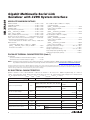
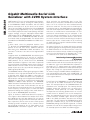
ABSOLUTE MAXIMUM RATINGS
AVDD to AGND.....................................................-0.5V to +1.9V
LVDSVDD to AGND...............................................-0.5V to +3.9V
DVDD to GND.......................................................-0.5V to +1.9V
IOVDD to GND......................................................-0.5V to +3.9V
Any Ground to Any Ground..................................-0.5V to +0.5V
RXIN_ _, RXCLKIN_ to AGND...............................-0.5V to +3.9V
OUT+, OUT- to AGND..........................................-0.5V to +1.9V
LMN_ to AGND (15mA current limit).....................-0.5V to +3.9V
All Other Pins to Any Ground............... -0.5V to (VIOVDD + 0.5V)
OUT+, OUT- Short Circuit to Ground or Supply........Continuous
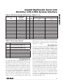
Continuous Power Dissipation (TA = +70NC)
48-Pin TQFP (derate 36.2mW/NC above +70NC).....2898.6mW
ESD Protection
Human Body Model (RD = 1.5kω, CS = 100pF)
(RXIN_ _, RXCLKIN_, OUT+, OUT-) to AGND.................±8kV
All Other Pins to GND.......................................................±3kV
IEC 61000-4-2 (RD = 330ω, CS = 150pF)
Contact Discharge
(RXIN_ _, RXCLKIN_) to AGND........................................±4kV
(OUT+, OUT-) to AGND.................................................±10kV
Air Discharge
(RXIN_ _, RXCLKIN_) to AGND........................................±8kV
(OUT+, OUT-) to AGND.................................................±12kV
ISO 10605 (RD = 2kω, CS = 330pF)
Contact Discharge
(RXIN_ _, RXCLKIN_) to AGND........................................±6kV
(OUT+, OUT-) to AGND.................................................±10kV
Air Discharge
(RXIN_ _, RXCLKIN_) to AGND......................................±20kV
(OUT+, OUT-) to AGND.................................................±30kV
Operating Temperature Range......................... -40NC to +105NC
Junction Temperature......................................................+150NC
Storage Temperature Range............................. -65NC to +150NC
Lead Temperature (soldering, 10s).................................+300NC
Soldering Temperature (reflow).......................................+260NC
PACKAGE THERMAL CHARACTERISTICS (Note 1)
48 TQFP-EP
Junction-to-Ambient Thermal Resistance (θJA)........27.6NC/W
Junction-to-Case Thermal Resistance (θJC).................2NC/W
Note 1: Package thermal resistances were obtained using the method described in JEDEC specification JESD51-7, using a fourlayer board. For detailed information on package thermal considerations, refer to www.maxim-ic.com/thermal-tutorial.
Stresses beyond those listed under “Absolute Maximum Ratings” may cause permanent damage to the device. These are stress ratings only, and functional
operation of the device at these or any other conditions beyond those indicated in the operational sections of the specifications is not implied. Exposure to absolute
maximum rating conditions for extended periods may affect device reliability.
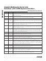
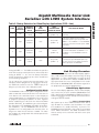
DC ELECTRICAL CHARACTERISTICS
(VDVDD = VAVDD = 1.7V to 1.9V, VLVDSVDD = 3.0V to 3.6V, VIOVDD = 1.7V to 3.6V, RL = 100I ±1% (differential), TA = -40NC to
+105NC, unless otherwise noted. Differential input voltage |VID| = 0.1V to 1.2V, input common-mode voltage VCM = |VID/2| to 2.4V
- |VID/2|. Typical values are at VDVDD = VAVDD = VIOVDD = 1.8V, VLVDSVDD = 3.3V, TA = +25NC.)
PARAMETER
SYMBOL
CONDITIONS
MIN
TYP
MAX
UNITS
SINGLE-ENDED INPUTS (PWDN, SSEN, BWS, DRS, MS, CDS, AUTOS, SD/CNTL0, SCK, WS, CNTL_)
High-Level Input Voltage
PWDN, SSEN, BWS, DRS, MS, CDS, AUTOS
0.65 x
VIOVDD
SD/CNTL0, SCK, WS, CNTL_
0.7 x
VIOVDD
VIH1
Low-Level Input Voltage
VIL1
Input Current
IIN1
Input Clamp Voltage
VCL
VIN = 0 to VIOVDD
ICL = -18mA
V
-10
0.35 x
VIOVDD
V
+10
FA
-1.5
V
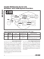
SINGLE-ENDED OUTPUT (INT)
High-Level Output Voltage
VOH1
IOH = -2mA
Low-Level Output Voltage
VOL1
IOL = 2mA
Output Short-Circuit Current
IOS
VO = 0V
VIOVDD 0.2
V
0.2
VIOVDD = 3.0V to 3.6V
16
35
64
VIOVDD = 1.7V to 1.9V
3
12
21
2 _______________________________________________________________________________________
V
mA