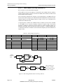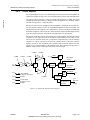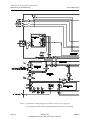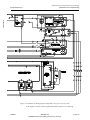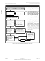
1
TECHNICAL MANUAL
APEXTM Exciter
Incorporating FLOTM Technology
888-2604-001
T.M. No. 888-2604-001
© Copyright Harris Corporation 2007
All rights reserved
Printed: January 25, 2007
Revision A, 03/08/07
APEX™ Exciter Incorporating FLO™ Technology
Returns And Exchanges
Damaged or undamaged equipment should not be returned unless written approval and a
Return Authorization is received from HARRIS CORPORATION, Broadcast Systems
Division. Special shipping instructions and coding will be provided to assure proper
handling. Complete details regarding circumstances and reasons for return are to be
included in the request for return. Custom equipment or special order equipment is not
returnable. In those instances where return or exchange of equipment is at the request of the
customer, or convenience of the customer, a restocking fee will be charged. All returns will
be sent freight prepaid and properly insured by the customer. When communicating with
HARRIS CORPORATION, Broadcast Division, specify the HARRIS Order Number or
Invoice Number.
Unpacking
Carefully unpack the equipment and preform a visual inspection to determine that no
apparent damage was incurred during shipment. Retain the shipping materials until it has
been determined that all received equipment is not damaged. Locate and retain all
PACKING CHECK LISTs. Use the PACKING CHECK LIST to help locate and identify
any components or assemblies which are removed for shipping and must be reinstalled.
Also remove any shipping supports, straps, and packing materials prior to initial turn on.
Technical Assistance
HARRIS Technical and Troubleshooting assistance is available from HARRIS Field
Service during normal business hours (8:00 AM - 5:00 PM Central Time). Emergency
service is available 24 hours a day. Telephone 217/222-8200 to contact the Field Service
Department or address correspondence to Field Service Department, HARRIS CORPORATION, Broadcast Systems Division, P.O. Box 4290, Quincy, Illinois 62305-4290,
USA. The HARRIS factory may also be contacted through a FAX facility (217/222-7041)
or a TELEX service (650/372-2976).
Replaceable Parts Service
Replacement parts are available 24 hours a day, seven days a week from the HARRIS
Service Parts Department. Telephone 217/222-8200 to contact the service parts department
or address correspondence to Service Parts Department, HARRIS CORPORATION,
Broadcast Systems Division, P.O. Box 4290, Quincy, Illinois 62305-4290, USA. The
HARRIS factory may also be contacted through a FAX facility (217/222-7041) or a
TELEX service (650/372-2976).
NOTE
The # symbol used in the parts list means used with (e.g. #C001 =
used with C001)
888-2604-001
WARNING: Disconnect primary power prior to servicing.
March 8, 2007
2604ti.fm
APEX™ Exciter Incorporating FLO™ Technology
Rev.
A
Date
3/8/07
March 8, 2007
ECN
54395
MANUAL REVISION HISTORY
APEX™ Exciter Incorporating FLO™ Technology
888-2604-001
Pages Affected
Released Manual
888-2604-001
WARNING: Disconnect primary power prior to servicing.
Page: i
APEX™ Exciter Incorporating FLO™ Technology
Page: ii
888-2604-001
WARNING: Disconnect primary power prior to servicing.
March 8, 2007
APEX™ Exciter Incorporating FLO™ Technology
2604ti.fm
Guide to Using Harris Parts List Information
The Harris Replaceable Parts List Index portrays a tree structure with the major items being leftmost in the index.
The example below shows the Transmitter as the highest item in the tree structure. If you were to look at the bill of
materials table for the Transmitter you would find the Control Cabinet, the PA Cabinet, and the Output Cabinet. In
the Replaceable Parts List Index the Control Cabinet, PA Cabinet, and Output Cabinet show up one indentation level
below the Transmitter and implies that they are used in the Transmitter. The Controller Board is indented one level
below the Control Cabinet so it will show up in the bill of material for the Control Cabinet. The tree structure of this
same index is shown to the right of the table and shows indentation level versus tree structure level.
Example of Replaceable Parts List Index and equivalent tree structure:
The part number of the item is shown to the right of the description as is the page in the manual where the bill for
that part number starts.
Inside the actual tables, four main headings are used:
Table #-#. ITEM NAME - HARRIS PART NUMBER - this line gives the information that corresponds to the
Replaceable Parts List Index entry;
HARRIS P/N column gives the ten digit Harris part number (usually in ascending order);
DESCRIPTION column gives a 25 character or less description of the part number;
REF. SYMBOLS/EXPLANATIONS column 1) gives the reference designators for the item (i.e., C001, R102,
etc.) that corresponds to the number found in the schematics (C001 in a bill of material is equivalent to C1 on the
schematic) or 2) gives added information or further explanation (i.e., “Used for 208V operation only,” or “Used
for HT 10LS only,” etc.).
Inside the individual tables some standard conventions are used:
A # symbol in front of a component such as #C001 under the REF. SYMBOLS/EXPLANATIONS column means
that this item is used on or with C001 and is not the actual part number for C001.
In the ten digit part numbers, if the last three numbers are 000, the item is a part that Harris has purchased and
has not manufactured or modified. If the last three numbers are other than 000, the item is either manufactured by
Harris or is purchased from a vendor and modified for use in the Harris product.
The first three digits of the ten digit part number tell which family the part number belongs to - for example, all
electrolytic (can) capacitors will be in the same family (524 xxxx 000). If an electrolytic (can) capacitor is found
to have a 9xx xxxx xxx part number (a number outside of the normal family of numbers), it has probably been
modified in some manner at the Harris factory and will therefore show up farther down into the individual parts
list (because each table is normally sorted in ascending order). Most Harris made or modified assemblies will
have 9xx xxxx xxx numbers associated with them.
The term “SEE HIGHER LEVEL BILL” in the description column implies that the reference designated part
number will show up in a bill that is higher in the tree structure. This is often the case for components that may
be frequency determinant or voltage determinant and are called out in a higher level bill structure that is more
customer dependent than the bill at a lower level.
March 8, 2007
888-2604-001
WARNING: Disconnect primary power prior to servicing.
Page: iii
APEX™ Exciter Incorporating FLO™ Technology
Page: iv
888-2604-001
WARNING: Disconnect primary power prior to servicing.
March 8, 2007
APEX™ Exciter Incorporating FLO™ Technology
WARNING
The currents and voltages in this equipment are dangerous. Personnel must at all times observe safety warnings, instructions and regulations.
2604ti.fm
This manual is intended as a general guide for trained and qualified personnel who are
aware of the dangers inherent in handling potentially hazardous electrical/electronic
circuits. It is not intended to contain a complete statement of all safety precautions which
should be observed by personnel in using this or other electronic equipment.
The installation, operation, maintenance and service of this equipment involves risks both
to personnel and equipment, and must be performed only by qualified personnel exercising
due care. HARRIS CORPORATION shall not be responsible for injury or damage
resulting from improper procedures or from the use of improperly trained or inexperienced
personnel performing such tasks.
During installation and operation of this equipment, local building codes and fire protection standards must be observed. The following National Fire Protection Association
(NFPA) standards are recommended as reference:
• Automatic Fire Detectors, No. 72E
• Installation, Maintenance, and Use of Portable Fire Extinguishers, No. 10
• Halogenated Fire Extinguishing Agent Systems, No. 12A
WARNING
Always disconnect power before opening covers, doors, enclosures,
gates, panels or shields. Always use grounding sticks and short out
high voltage points before servicing. Never make internal adjustments, perform maintenance or service when alone or when fatigued.
Do not remove, short-circuit or tamper with interlock switches on access covers, doors,
enclosures, gates, panels or shields. Keep away from live circuits, know your equipment
and don’t take chances.
WARNING
In case of emergency ensure that power has been disconnected.
If oil filled or electrolytic capacitors are utilized in your equipment, and if a leak or bulge
is apparent on the capacitor case when the unit is opened for service or maintenance, allow
the unit to cool down before attempting to remove the defective capacitor. Do not attempt
to service a defective capacitor while it is hot due to the possibility of a case rupture and
subsequent injury.
March 8, 2007
888-2604-001
WARNING: Disconnect primary power prior to servicing.
Page: v
APEX™ Exciter Incorporating FLO™ Technology
Page: vi
888-2604-001
WARNING: Disconnect primary power prior to servicing.
March 8, 2007
APEX™ Exciter Incorporating FLO™ Technology
FIRST-AID
2604ti.fm
Personnel engaged in the installation, operation, maintenance or servicing of this
equipment are urged to become familiar with first-aid theory and practices. The following
information is not intended to be complete first-aid procedures, it is a brief and is only to
be used as a reference. It is the duty of all personnel using the equipment to be prepared to
give adequate Emergency First Aid and thereby prevent avoidable loss of life.
Treatment of Electrical Burns
1.
Extensive burned and broken skin
A. Cover area with clean sheet or cloth. (Cleanest available cloth article.)
B. Do not break blisters, remove tissue, remove adhered particles of clothing, or
apply any salve or ointment.
C. Treat victim for shock as required.
D. Arrange transportation to a hospital as quickly as possible.
E. If arms or legs are affected keep them elevated.
NOTE
If medical help will not be available within an hour and the victim
is conscious and not vomiting, give him a weak solution of salt and
soda: 1 level teaspoonful of salt and 1/2 level teaspoonful of baking
soda to each quart of water (neither hot or cold). Allow victim to sip
slowly about 4 ounces (a half of glass) over a period of 15 minutes.
Discontinue fluid if vomiting occurs. (Do not give alcohol.)
2.
Less severe burns - (1st & 2nd degree)
A. Apply cool (not ice cold) compresses using the cleanest available cloth article.
B. Do not break blisters, remove tissue, remove adhered particles of clothing, or
apply salve or ointment.
C. Apply clean dry dressing if necessary.
D. Treat victim for shock as required.
E. Arrange transportation to a hospital as quickly as possible.
F. If arms or legs are affected keep them elevated.
REFERENCE
ILLINOIS HEART ASSOCIATION
AMERICAN RED CROSS STANDARD FIRST AID AND PERSONAL SAFETY
MANUAL (SECOND EDITION)
March 8, 2007
888-2604-001
WARNING: Disconnect primary power prior to servicing.
Page: vii
APEX™ Exciter Incorporating FLO™ Technology
Page: viii
888-2604-001
WARNING: Disconnect primary power prior to servicing.
March 8, 2007
APEX™ Exciter Incorporating FLO™ Technology
Table of Contents
Table of Contents
2604s100TOC.fm
1
2
Introduction . . . . . . . . . . . . . . . . . . . . . . . . . . . . . . . . . . . . . . . . 1-1
1.1
Organization of Technical Manual . . . . . . . . . . . . . . . . . . 1-1
1.2
General Description . . . . . . . . . . . . . . . . . . . . . . . . 1-1
1.3
Physical Description . . . . . . . . . . . . . . . . . . . . . . . . 1-2
1.4
Technical Overview . . . . . . . . . . . . . . . . . . . . . . . . 1-4
1.5
Specifications . . . . . . . . . . . . . . . . . . . . . . . . . . 1-4
Installation . . . . . . . . . . . . . . . . . . . . . . . . . . . . . . . . . . . . . . . . 2-1
2.1
Introduction . . . . . . . . . . . . . . . . . . . . . . . . . . . 2-1
2.2
Installing Exciters Removed for Shipment . . . . . . . . . . . . . . . 2-1
2.3
Signal Connections . . . . . . . . . . . . . . . . . . . . . . . . 2-1
2.3.1
AC Power . . . . . . . . . . . . . . . . . . . . . . . . . . . . . . . . .2-2
2.4
Installation of the GPS 1PPS Signal . . . . . . . . . . . . . . . . . . 2-2
2.5
Retrofitting Into Existing Transmitter System . . . . . . . . . . . . . . 2-3
2.5.1
Feedback Requirements . . . . . . . . . . . . . . . . . . . . . . . . . .2-3
2.5.1.1
2.6
2.7
3
2.5.2
Typical Transmitter Systems Block Diagrams . . . . . . . . . . . . . .2-4
2.5.3
Atlas Mobile Transmitters . . . . . . . . . . . . . . . . . . . . . . . .2-5
2.5.3.1
Atlas Mobile Transmitter - 1 PA Cabinet, 2 Exciters . . . . .2-5
2.5.3.2
Atlas Mobile Transmitter - 2 or More PA Cabinets. . . . . .2-6
Configuring the Exciter . . . . . . . . . . . . . . . . . . . . . . . 2-7
2.6.1
Configuration of Setup Screens . . . . . . . . . . . . . . . . . . . . . .2-7
2.6.2
Configuration of Status Screens. . . . . . . . . . . . . . . . . . . . . .2-9
2.6.3
Normal Settings for Diagnostic Screens . . . . . . . . . . . . . . . . 2-10
Materials Needed . . . . . . . . . . . . . . . . . . . . . . . . .2-11
Navigating the LCD Display Screens . . . . . . . . . . . . . . . . . . . . . . . . . . 3-1
3.1
Basic Operating Procedure . . . . . . . . . . . . . . . . . . . . . 3-1
3.1.1
Raising or Lowering Output Power . . . . . . . . . . . . . . . . . . . .3-1
3.1.2
Exciter Fault Display - Red . . . . . . . . . . . . . . . . . . . . . . . .3-1
3.1.2.1
3.2
3.3
03/08/07
Feedback Signal Quality Requirements. . . . . . . . . . . .2-4
Fault Warning - Yellow . . . . . . . . . . . . . . . . . . . .3-1
Starting Point: The Main LCD Touch Screen . . . . . . . . . . . . . . 3-2
3.2.1
Spectrum Response Screen . . . . . . . . . . . . . . . . . . . . . . . .3-3
3.2.2
Exciter Status Series of Screens. . . . . . . . . . . . . . . . . . . . . .3-3
3.2.3
Exciter Setup Series of Screens . . . . . . . . . . . . . . . . . . . . . .3-3
3.2.4
FLO Measure Soft Key . . . . . . . . . . . . . . . . . . . . . . . . . .3-4
LCD Display Flow Chart . . . . . . . . . . . . . . . . . . . . . . 3-4
888-2604-001
WARNING: Disconnect primary power prior to servicing.
Page: ix
APEX™ Exciter Incorporating FLO™ Technology
Table of Contents
3.4
Details of the Exciter Status Screens. . . . . . . . . . . . . . . . . . 3-8
3.4.1
System Status Screen . . . . . . . . . . . . . . . . . . . . . . . . . . .3-8
3.4.2
Transport Stream Status Screen . . . . . . . . . . . . . . . . . . . . . .3-9
3.4.3
Adaptive Processing Board Status Screen . . . . . . . . . . . . . . . .3-9
3.4.3.1
3.4.4
3.4.5
Adaptive Processing Diagnostics . . . . . . . . . . . . . . 3-11
Digital Processing Screens . . . . . . . . . . . . . . . . . . . . . . . 3-12
3.4.4.1
Modulator Board Status, Screen 1/2 . . . . . . . . . . . . 3-12
3.4.4.2
ADC and DAC Boards Status, Screen 2/2 . . . . . . . . . 3-13
3.4.4.3
FLO FPGA Status, Summary, Screen 1/5. . . . . . . . . . 3-14
3.4.4.4
FLO FPGA, GPS & Clock Status, Screen 2/5 . . . . . . . 3-15
3.4.4.5
FLO FPGA, Transport Stream Status, Screen 3/5 . . . . . 3-16
3.4.4.6
FLO FPGA, SFN FIFO Status, Screen 4/5 . . . . . . . . . 3-17
3.4.4.7
FLO FPGA, MTI Status, Screen 5/5 . . . . . . . . . . . . 3-18
IF & RF Processing Status Screens . . . . . . . . . . . . . . . . . . . 3-19
3.4.5.1
UDC Interface Board Status, Screen 1/4 . . . . . . . . . . 3-19
3.4.5.2
PLL Board Status Screen . . . . . . . . . . . . . . . . . . 3-20
3.4.5.2.1
3.4.5.3
3-22
Down Converter Diagnostics
3-24
System Control Status Screens . . . . . . . . . . . . . . . . . . . . . 3-25
3.4.6.1
Controller Board Status Screen . . . . . . . . . . . . . . . 3-26
3.4.6.1.1
3.4.6.2
3.4.6.3
Controller Board Diagnostics
3-26
External I/O Board Status Screen . . . . . . . . . . . . . . 3-27
3.4.6.2.1
External I/O Diagnostics
3-28
CAN Bus Status Screen . . . . . . . . . . . . . . . . . . . 3-30
3.4.6.3.1
CAN Diagnostics
3-30
3.4.6.4
Front Panel Board Status Screen . . . . . . . . . . . . . . 3-30
3.4.6.5
GPS Status Screen. . . . . . . . . . . . . . . . . . . . . . 3-31
3.5
Built In Tests . . . . . . . . . . . . . . . . . . . . . . . . . . .3-32
3.6
Details of the System Setup Screens . . . . . . . . . . . . . . . . . .3-32
3.6.1
Restore Defaults Operation . . . . . . . . . . . . . . . . . . . . . . . 3-33
3.6.2
Exciter Setup Screen . . . . . . . . . . . . . . . . . . . . . . . . . . 3-35
3.6.2.1
3.6.3
Page: x
Up Converter Diagnostics
Down Converter Board Status Screen . . . . . . . . . . . 3-23
3.4.5.4.1
3.4.6
3-21
Up Converter Board Status Screen . . . . . . . . . . . . . 3-21
3.4.5.3.1
3.4.5.4
PLL Diagnostics
Power Calibration . . . . . . . . . . . . . . . . . . . . . . 3-38
RTAC Setup Screen . . . . . . . . . . . . . . . . . . . . . . . . . . . 3-38
888-2604-001
WARNING: Disconnect primary power prior to servicing.
03/08/07
2604s100TOC.fm
APEX™ Exciter Incorporating FLO™ Technology
Table of Contents
Max Peak Stretch . . . . . . . . . . . . . . . . . . . . . . 3-40
3.6.3.3
RTAC Power On Mode . . . . . . . . . . . . . . . . . . . 3-40
3.6.3.4
RTAC Off Air Mode . . . . . . . . . . . . . . . . . . . . 3-41
3.6.5
External I/O Setup Screen. . . . . . . . . . . . . . . . . . . . . . . . 3-42
3.6.8
3.6.9
03/08/07
3.6.3.2
Display Setup Screen . . . . . . . . . . . . . . . . . . . . . . . . . . 3-41
3.6.7
4
Filter Type. . . . . . . . . . . . . . . . . . . . . . . . . . 3-40
3.6.4
3.6.6
3.7
3.6.3.1
3.6.5.1
VSWR Foldback Parameters . . . . . . . . . . . . . . . . 3-43
3.6.5.2
RF Present Cutoff . . . . . . . . . . . . . . . . . . . . . . 3-43
3.6.5.3
External I/O Interface to Transmitter Control Logic . . . . 3-44
Serial I/O Setup Screens . . . . . . . . . . . . . . . . . . . . . . . . 3-45
3.6.6.1
Serial Setup Screen 1 of 3, RS-232 . . . . . . . . . . . . . 3-45
3.6.6.2
Serial Setup Screen 2 of 3, Ethernet . . . . . . . . . . . . 3-46
3.6.6.3
Serial Setup Screen 3 of 3, CAN . . . . . . . . . . . . . . 3-47
FPGA Setup . . . . . . . . . . . . . . . . . . . . . . . . . . . . . . . 3-48
3.6.7.1
FPGA Configure 1/5 . . . . . . . . . . . . . . . . . . . . 3-48
3.6.7.2
FPGA Configure 2/5 . . . . . . . . . . . . . . . . . . . . 3-49
3.6.7.3
FPGA Configure 3/5 . . . . . . . . . . . . . . . . . . . . 3-50
3.6.7.4
FPGA Configure 4/5 . . . . . . . . . . . . . . . . . . . . 3-51
3.6.7.5
FPGA Configure 5/5, Restore Defaults . . . . . . . . . . . 3-52
Change Passwords > Security Setup . . . . . . . . . . . . . . . . . . 3-53
3.6.8.1
User Setup (Locked or Unlocked) . . . . . . . . . . . . . 3-54
3.6.8.2
Diagnostics Setup (Locked or Unlocked) . . . . . . . . . . 3-54
3.6.8.3
Factory Setup (Locked or Unlocked) . . . . . . . . . . . . 3-55
Restore Defaults . . . . . . . . . . . . . . . . . . . . . . . . . . . . . 3-55
RTAC Operating Procedures, Main Screen. . . . . . . . . . . . . . . .3-55
3.7.1
From RTAC Section of Main Screen . . . . . . . . . . . . . . . . . . 3-55
3.7.2
From Adaptive Precorrection Board Status Screen . . . . . . . . . . . 3-56
3.7.3
From Down Converter Board Status Screen . . . . . . . . . . . . . . 3-56
3.7.4
From Down Converter Diagnostics Screen . . . . . . . . . . . . . . . 3-56
3.7.5
From RTAC Setup Screen . . . . . . . . . . . . . . . . . . . . . . . 3-57
Theory of Operation . . . . . . . . . . . . . . . . . . . . . . . . . . . . . . . . . . . 4-1
4.1
General Description . . . . . . . . . . . . . . . . . . . . . . . . 4-1
4.2
Transmitter Systems Block Diagram. . . . . . . . . . . . . . . . . . 4-1
4.3
APEX Exciter Digital Assembly Overview . . . . . . . . . . . . . . . 4-2
4.3.1
Controller Board Theory . . . . . . . . . . . . . . . . . . . . . . . . .4-3
4.3.2
RTAC and Adaptive Precorrector Board Theory . . . . . . . . . . . . .4-5
888-2604-001
WARNING: Disconnect primary power prior to servicing.
Page: xi
APEX™ Exciter Incorporating FLO™ Technology
Table of Contents
4.3.2.1
4.3.3
4.4
Exciter Output Spectral Response, RTAC Bypassed . . . . . . . . . . .4-6
APEX Exciter Analog Assembly Overview . . . . . . . . . . . . . . . 4-7
4.4.1
Up Converter Board Block Diagram Description. . . . . . . . . . . . .4-8
4.4.1.1
Down Converter Board Block Diagram Description . . . . . . . . . . .4-9
4.4.3
PLL Board - A4 . . . . . . . . . . . . . . . . . . . . . . . . . . . . . 4-10
10 MHz Reference . . . . . . . . . . . . . . . . . . . . . 4-10
4.4.3.2
128.9 MHz IF PLL (First L. O.) . . . . . . . . . . . . . . 4-11
4.4.3.3
Main Phase Lock Loop (Second LO) . . . . . . . . . . . . 4-12
Output Amplifier . . . . . . . . . . . . . . . . . . . . . . . . . . . . 4-13
4.5.1
Main Power Supply . . . . . . . . . . . . . . . . . . . . . . . . . . . 4-14
4.5.2
Digital Deck Power . . . . . . . . . . . . . . . . . . . . . . . . . . . 4-14
4.5.2.1
Controller Board Power . . . . . . . . . . . . . . . . . . . 4-14
4.5.2.2
FPGA Modulator Board Power . . . . . . . . . . . . . . . 4-15
4.5.2.3
Adaptive Processing Board Power . . . . . . . . . . . . . 4-15
4.5.2.4
Power for DAC and ADC Boards. . . . . . . . . . . . . . 4-15
4.5.2.5
External I/O Board Power. . . . . . . . . . . . . . . . . . 4-16
4.5.2.6
Front Panel Board . . . . . . . . . . . . . . . . . . . . . . 4-16
Analog Deck Power . . . . . . . . . . . . . . . . . . . . . . . . . . . 4-16
4.5.3.1
UDC Interface Board Power . . . . . . . . . . . . . . . . 4-16
4.5.3.2
Exciter Cooling Fan Power . . . . . . . . . . . . . . . . . 4-16
4.5.3.3
Down Converter Board Power . . . . . . . . . . . . . . . 4-17
4.5.3.4
PLL Board Power . . . . . . . . . . . . . . . . . . . . . . 4-17
4.5.3.5
Up Converter Board Power . . . . . . . . . . . . . . . . . 4-18
4.5.3.6
Output Amplifier . . . . . . . . . . . . . . . . . . . . . . 4-18
Maintenance and Troubleshooting . . . . . . . . . . . . . . . . . . . . . . . . . . . . 5-1
5.1
5.2
Page: xii
4.4.3.1
DC Power Distribution . . . . . . . . . . . . . . . . . . . . . . .4-14
4.5.3
5
Up Converter Board UHF/VHF Band Pass Filter. . . . . . .4-8
4.4.2
4.4.4
4.5
44.4 MHz Phase Lock Loop . . . . . . . . . . . . . . . . .4-6
Exciter Maintenance . . . . . . . . . . . . . . . . . . . . . . . . 5-1
5.1.1
Cleaning . . . . . . . . . . . . . . . . . . . . . . . . . . . . . . . . . .5-1
5.1.2
Measuring PLL Board Frequencies . . . . . . . . . . . . . . . . . . . .5-6
5.1.2.1
Measuring Center Channel Frequency . . . . . . . . . . . .5-6
5.1.2.2
PLL Board 10 MHz Reference Oscillator Frequency. . . . .5-8
5.1.2.3
Measuring the 1st Local Oscillator Frequency . . . . . . . .5-8
5.1.2.4
Measuring the 2nd Local Oscillator Frequency . . . . . . . .5-8
Loading Software . . . . . . . . . . . . . . . . . . . . . . . . . 5-9
888-2604-001
WARNING: Disconnect primary power prior to servicing.
03/08/07
2604s100TOC.fm
APEX™ Exciter Incorporating FLO™ Technology
Table of Contents
5.3
Default Settings For DIagnostics Screens . . . . . . . . . . . . . . . .5-10
5.4
Typical Settings for the More Critical Exciter Setups . . . . . . . . . . .5-11
5.5
Exciter Troubleshooting Flow Charts . . . . . . . . . . . . . . . . .5-12
5.6
General Troubleshooting . . . . . . . . . . . . . . . . . . . . . .5-16
5.6.1
5.7
5.8
System Troubleshooting . . . . . . . . . . . . . . . . . . . . . .5-17
5.7.1
PA, HPF, or ADC Adaptive Processing Faults . . . . . . . . . . . . . 5-17
5.7.2
Transmitter Response Not Conforming to Mask Requirements . . . . 5-17
5.7.3
Checking Transmitter Spectrum . . . . . . . . . . . . . . . . . . . . 5-18
5.7.4
ASI Transport Stream Faults . . . . . . . . . . . . . . . . . . . . . . 5-18
Exciter Troubleshooting . . . . . . . . . . . . . . . . . . . . . .5-19
5.8.1
Frequency Error . . . . . . . . . . . . . . . . . . . . . . . . . . . . . 5-19
5.8.2
Dark Screen . . . . . . . . . . . . . . . . . . . . . . . . . . . . . . . 5-19
5.8.3
Power Supply Voltages . . . . . . . . . . . . . . . . . . . . . . . . . 5-20
5.8.4
Troubleshooting Down to the Board Level . . . . . . . . . . . . . . . 5-21
5.8.5
5.8.6
5.8.7
6
Troubleshooting Tips . . . . . . . . . . . . . . . . . . . . . . . . . . 5-16
5.8.4.1
Digital Tray Transmission Data Path . . . . . . . . . . . . 5-21
5.8.4.2
Analog Tray Signal Path . . . . . . . . . . . . . . . . . . 5-21
Isolating Problem to the Analog or Digital Tray . . . . . . . . . . . . 5-21
5.8.5.1
Checking Operation of the Entire Digital Tray . . . . . . . 5-21
5.8.5.2
Checking Operation of the Entire Exciter. . . . . . . . . . 5-22
Isolating a Faulty Board in the Digital Tray . . . . . . . . . . . . . . 5-23
5.8.6.1
Modulator Board . . . . . . . . . . . . . . . . . . . . . . 5-23
5.8.6.2
Adaptive Precorrector Board . . . . . . . . . . . . . . . . 5-24
5.8.6.3
ADC and DAC Boards . . . . . . . . . . . . . . . . . . . 5-24
5.8.6.4
Front Panel Board . . . . . . . . . . . . . . . . . . . . . . 5-24
5.8.6.5
Controller Board . . . . . . . . . . . . . . . . . . . . . . 5-24
Analog Tray Troubleshooting . . . . . . . . . . . . . . . . . . . . . . 5-25
Parts List . . . . . . . . . . . . . . . . . . . . . . . . . . . . . . . . . . . . . . . . . 6-1
Appendix AExciter GUI Screen Captures. . . . . . . . . . . . . . . . . . . . . . . . . . . A-1
03/08/07
888-2604-001
WARNING: Disconnect primary power prior to servicing.
Page: xiii
APEX™ Exciter Incorporating FLO™ Technology
Table of Contents
Page: xiv
888-2604-001
WARNING: Disconnect primary power prior to servicing.
03/08/07
APEX™ Exciter Incorporating FLO™ Technology
List of Figures
2604s100LOF.fm
List of Figures
Figure 1-1
Rear Panel View APEX Exciter Incorporating FLO Technology . . . . . . . . . 1-2
Figure 1-2
APEX Exciter Front Panel View . . . . . . . . . . . . . . . . . . . . . . . . . . 1-3
Figure 2-1
Exciter Inputs and Outputs . . . . . . . . . . . . . . . . . . . . . . . . . . . . . 2-2
Figure 2-2
1PPS Signal Termination Methods. . . . . . . . . . . . . . . . . . . . . . . . . 2-3
Figure 2-3
Atlas Mobile Transmitter - Single PA Cabinet - Dual Exciters . . . . . . . . . . 2-5
Figure 2-4
Atlas Mobile Transmitter - Dual PA Cabinets - Dual Exciters. . . . . . . . . . . 2-6
Figure 3-1
LCD Main Screen . . . . . . . . . . . . . . . . . . . . . . . . . . . . . . . . . 3-2
Figure 3-2
APEX Exciter LCD Display Flow Chart, Main Screen . . . . . . . . . . . . . . 3-5
Figure 3-3
APEX Exciter LCD Display Flow Chart, Status Screens . . . . . . . . . . . . . 3-6
Figure 3-4
APEX Exciter LCD Display Flow Chart, Setup Screens. . . . . . . . . . . . . . 3-7
Figure 3-5
System Status Screen . . . . . . . . . . . . . . . . . . . . . . . . . . . . . . . . 3-8
Figure 3-6
Transport Stream Status Screen . . . . . . . . . . . . . . . . . . . . . . . . . . 3-9
Figure 3-7
Adaptive Processing Board Status Screen . . . . . . . . . . . . . . . . . . . . . 3-9
Figure 3-8
Adaptive Processing Diagnostics. . . . . . . . . . . . . . . . . . . . . . . . . .3-11
Figure 3-9
Modulation Board Status Screen . . . . . . . . . . . . . . . . . . . . . . . . . .3-12
Figure 3-10 Modulation Board Status, Screen 1/2 . . . . . . . . . . . . . . . . . . . . . . .3-12
Figure 3-11 ADC and DAC Status, Screen 2/2 . . . . . . . . . . . . . . . . . . . . . . . . .3-13
Figure 3-12 FLO FPGA Status, Summary, Screen 1/5 . . . . . . . . . . . . . . . . . . . . .3-14
Figure 3-13 FLO FPGA, GPS & Clock Status, Screen 2/5 . . . . . . . . . . . . . . . . . . .3-15
Figure 3-14 FLO FPGA, Transport Stream Status Screen 3/5 . . . . . . . . . . . . . . . . .3-16
Figure 3-15 FLO FPGA, FSN FIFO Status, Screen 4/5 . . . . . . . . . . . . . . . . . . . . .3-17
Figure 3-16 FLO FPGA, MTI Status, Screen 5/5 . . . . . . . . . . . . . . . . . . . . . . . .3-18
Figure 3-17 UDC Interface Board Status, Screen 1/4 . . . . . . . . . . . . . . . . . . . . . .3-19
Figure 3-18 PLL Board Status Screen . . . . . . . . . . . . . . . . . . . . . . . . . . . . . .3-20
Figure 3-19 PLL Diagnostics . . . . . . . . . . . . . . . . . . . . . . . . . . . . . . . . . .3-21
Figure 3-20 Up Converter Board Status Screen . . . . . . . . . . . . . . . . . . . . . . . . .3-21
Figure 3-21 Up Converter Diagnostics . . . . . . . . . . . . . . . . . . . . . . . . . . . . .3-22
Figure 3-22 Down Converter Board Status Screen . . . . . . . . . . . . . . . . . . . . . . .3-23
Figure 3-23 Down Converter Diagnostics . . . . . . . . . . . . . . . . . . . . . . . . . . . .3-24
Figure 3-24 Controller Board Status Screen. . . . . . . . . . . . . . . . . . . . . . . . . . .3-26
Figure 3-25 External I/O Board Status Screen . . . . . . . . . . . . . . . . . . . . . . . . .3-27
Figure 3-26 External I/O Diagnostics . . . . . . . . . . . . . . . . . . . . . . . . . . . . . .3-28
Figure 3-27 CAN Bus Status Screen . . . . . . . . . . . . . . . . . . . . . . . . . . . . . .3-30
Figure 3-28 Front Panel Board Status Screen . . . . . . . . . . . . . . . . . . . . . . . . . .3-30
Figure 3-29 Front Panel Board Status Screen . . . . . . . . . . . . . . . . . . . . . . . . . .3-31
03/08/07
888-2604-001
WARNING: Disconnect primary power prior to servicing.
Page: xv
APEX™ Exciter Incorporating FLO™ Technology
List of Figures
Figure 3-30 Built In Tests Screen . . . . . . . . . . . . . . . . . . . . . . . . . . . . . . . .3-32
Figure 3-31 System Setup Screen . . . . . . . . . . . . . . . . . . . . . . . . . . . . . . . .3-32
Figure 3-32 Exciter Setup Screen . . . . . . . . . . . . . . . . . . . . . . . . . . . . . . . .3-35
Figure 3-33 Power Calibration Screen. . . . . . . . . . . . . . . . . . . . . . . . . . . . . .3-38
Figure 3-34 RTAC Setup Screen . . . . . . . . . . . . . . . . . . . . . . . . . . . . . . . .3-38
Figure 3-35 Display Setup Screen . . . . . . . . . . . . . . . . . . . . . . . . . . . . . . . .3-41
Figure 3-36 External I/O Setup Screen . . . . . . . . . . . . . . . . . . . . . . . . . . . . .3-42
Figure 3-37 Serial Setup Screen 1 of 3, RS-232. . . . . . . . . . . . . . . . . . . . . . . . .3-45
Figure 3-38 Serial Setup Screen 2 of 3, Ethernet . . . . . . . . . . . . . . . . . . . . . . . .3-46
Figure 3-39 Serial Setup Screen 3 of 3, CAN . . . . . . . . . . . . . . . . . . . . . . . . . .3-47
Figure 3-40 FPGA Configure 1/5 . . . . . . . . . . . . . . . . . . . . . . . . . . . . . . . .3-48
Figure 3-41 FPGA Configure 2/5 . . . . . . . . . . . . . . . . . . . . . . . . . . . . . . . .3-49
Figure 3-42 FPGA Configure 3/5 . . . . . . . . . . . . . . . . . . . . . . . . . . . . . . . .3-50
Figure 3-43 FPGA Configure 4/5 . . . . . . . . . . . . . . . . . . . . . . . . . . . . . . . .3-51
Figure 3-44 FPGA Configure 5/5, Restore Defaults . . . . . . . . . . . . . . . . . . . . . .3-52
Figure 3-45 Security Setup Screen . . . . . . . . . . . . . . . . . . . . . . . . . . . . . . .3-53
Figure 3-46 System Setup Screen . . . . . . . . . . . . . . . . . . . . . . . . . . . . . . . .3-54
Figure 4-1
APEX Exciter/ Transmitter - RF Interconnection Block Diagram . . . . . . . . . 4-2
Figure 4-2
APEX Exciter - Signal Flow Block Diagram . . . . . . . . . . . . . . . . . . . 4-4
Figure 4-3
The 44.4 MHz Phase Lock Loop . . . . . . . . . . . . . . . . . . . . . . . . . . 4-6
Figure 4-4
Exciter Output Spectral Response, RTAC Bypassed. . . . . . . . . . . . . . . . 4-7
Figure 4-5
Up Converter Simplified Block Diagram. . . . . . . . . . . . . . . . . . . . . . 4-9
Figure 4-6
Analog Assembly Detailed Block Diagram. . . . . . . . . . . . . . . . . . . . .4-10
Figure 4-7
10 MHz Reference Oscillator Block Diagram . . . . . . . . . . . . . . . . . . .4-11
Figure 4-8
Block Diagram First LO . . . . . . . . . . . . . . . . . . . . . . . . . . . . . .4-11
Figure 4-9
Block Diagram Main Phase Lock Loop (2nd LO) . . . . . . . . . . . . . . . . .4-12
Figure 4-10 Output RF Amplifier Block Diagram . . . . . . . . . . . . . . . . . . . . . . .4-13
Figure 5-1
Top View of Exciter (Analog Side) With Cover Removed . . . . . . . . . . . . 5-2
Figure 5-2
Bottom View of Exciter (Digital Side) With Cover Removed . . . . . . . . . . . 5-3
Figure 5-3
APEX Exciter Wiring Diagram, Left Side (see Figure 5-4 for right side) . . . . . 5-4
Figure 5-4
APEX Exciter Wiring Diagram, Right Side (see Figure 5-3 for left side) . . . . . 5-5
Figure 5-5
Frequency Error Troubleshooting Flow Chart . . . . . . . . . . . . . . . . . . .5-12
Figure 5-6
Low or No Output Power Troubleshooting Flow Chart . . . . . . . . . . . . . .5-13
Figure 5-7
Transmitter Fails Mask Test Troubleshooting Flow Chart. . . . . . . . . . . . .5-14
Figure 5-8
Transmitter Has Excessive MER Troubleshooting Flow Chart . . . . . . . . . .5-15
Figure 5-9
Exciter Output Spectral Response, RTAC Bypassed. . . . . . . . . . . . . . . .5-26
Page: xvi
888-2604-001
WARNING: Disconnect primary power prior to servicing.
03/08/07
APEX™ Exciter Incorporating FLO™ Technology
List of Figures
Figure A-1 Tera Term Pro Screen When Connected to Exciter . . . . . . . . . . . . . . . . A-2
Figure A-2 Stop Action Capture of Screen Down Load Scroll. . . . . . . . . . . . . . . . . A-2
2604s100LOF.fm
Figure A-3 Tera Term Log Window Selected When Download Has Completed . . . . . . . A-3
03/08/07
888-2604-001
WARNING: Disconnect primary power prior to servicing.
Page: xvii
APEX™ Exciter Incorporating FLO™ Technology
List of Figures
Page: xviii
888-2604-001
WARNING: Disconnect primary power prior to servicing.
03/08/07
APEX™ Exciter Incorporating FLO™ Technology
List of Tables
2604s100LOT.fm
List of Tables
03/08/07
Table 1-1
Harris APEX Exciter General Specifications . . . . . . . . . . . . . . . . . . . 1-4
Table 1-2
Harris APEX Exciter Service Conditions Specifications . . . . . . . . . . . . . 1-5
Table 1-3
Harris APEX Exciter Performance Specifications . . . . . . . . . . . . . . . . 1-6
Table 3-1
System Status Screen Circuit Board Names . . . . . . . . . . . . . . . . . . . . 3-8
Table 3-2
Location of System Setup Sub Screens . . . . . . . . . . . . . . . . . . . . . .3-33
Table 3-3
Settings Resulting From Restore Defaults Activation. . . . . . . . . . . . . . .3-33
Table 3-4
UHF External I/O Parallel Control Interface Connector J1 . . . . . . . . . . . .3-44
Table 4-1
Output Signal Bandwidth . . . . . . . . . . . . . . . . . . . . . . . . . . . . . 4-6
Table 4-2
2nd LO Output Frequencies . . . . . . . . . . . . . . . . . . . . . . . . . . . .4-12
Table 4-3
Exciter Power Supply Voltages . . . . . . . . . . . . . . . . . . . . . . . . . .4-14
Table 5-1
Diagnostics Screens Default Settings . . . . . . . . . . . . . . . . . . . . . . .5-10
Table 5-2
Typical Settings For Some of the More Critical Exciter Setup Functions . . . .5-11
Table 5-3
Exciter Power Supply Voltages . . . . . . . . . . . . . . . . . . . . . . . . . .5-20
Table 5-4
Analog Tray RF Input and Output levels . . . . . . . . . . . . . . . . . . . . .5-25
Table 5-5
Phase Noise Mask . . . . . . . . . . . . . . . . . . . . . . . . . . . . . . . . .5-26
Table 5-6
Output Signal Bandwidth . . . . . . . . . . . . . . . . . . . . . . . . . . . . .5-26
888-2604-001
WARNING: Disconnect primary power prior to servicing.
Page: xix
APEX™ Exciter Incorporating FLO™ Technology
List of Tables
Page: xx
888-2604-001
WARNING: Disconnect primary power prior to servicing.
03/08/07
Organization of Technical Manual
1
APEX™ Exciter Incorporating FLO™ Technology
Introduction
Introduction
2604s100.fm
This technical manual contains installation, operating and maintenance procedures for the
HARRIS APEX Exciter incorporating FLOTM technology1.
1.1
Organization of Technical Manual
The manual is divided into these sections:
• Section 1 - Introduction, describes the APEX exciter and lists the sections of this
technical manual.
• Section 2 - Installation, describes the mounting, environmental requirements and initial setup of the exciter.
• Section 3 - Navigating the LCD Display Screens, explains how to operate the exciter.
• Section 4 - APEX Exciter Theory, explains the functioning of each part of the exciter
as an aid to servicing the product.
• Section 5 - Maintenance and Troubleshooting, describes checks and test which may
be used to isolate a suspected problem in the exciter.
• Section 6 - Parts List, is an indexed listing of field-replaceable parts for the APEX exciter.
1.2
General Description
This APEX exciter s a low power transmitter signal source for the FLO technology
It receives the program material to be transmitted in the form of the ASI transport stream
and generates a low-level on-channel RF signal. It performs pre-corrections for signal
distortions which occur in the transmitter RF power amplifiers, high power filter, and
transmission line.
This APEX exciter incorporating FLO™ Technology is presently installed in the Harris
Ranger and Atlas Mobile transmitters, and can also be used as a stand alone signal source
for testing purposes.
FLO technology was designed for distribution of multimedia material. It uses orthogonal
frequency division multiplexing (OFDM). It achieves high spectral efficiency while
meeting mobility requirements (it can be received at speeds up to 200 km/hour) in a large
cell SFN (single frequency network). The FLO physical layer uses a 4K mode (yielding a
transform size of 4096 sub-carriers). The individual sub-carriers are modulated by QPSK
(quadrature phase shift keying) or 16-QAM (quadrature amplitude modulation).
OFDM modulation is also used by Digital Audio Broadcasting (DAB)2, Terrestrial Digital
Video Broadcasting (DVB-T)3, and Terrestrial Integrated Services Digital Broadcasting
(ISDB-T)4.
1. FLO is a trademark of QUALCOMM Inc.
2. Digital Audio Broadcasting (DAB) system also referred to as Eureka 147 and defined in ETSI EN 300
401: “Digital Audio Broadcasting (DAB); DAB to mobile, portable and fixed receivers.”
3. Terrestrial Digital Video Broadcasting (DVB-T) as defined in ETSI EN 300 744: “Digital Video Broadcasting (DVB); Framing structure, channel coding and modulation for digital terrestrial television.”
4. ISDB family includes System C of Recommendation ITU-R BT.1306, System F of Recommendation
ITU-R BS.1114 and IDSB-S of Recommendation ITU-R BO.1408
03/08/07
888-2604-001
WARNING: Disconnect primary power prior to servicing.
Page: 1-1
APEX™ Exciter Incorporating FLO™ Technology
Introduction
1.3
Physical Description
Physical Description
The APEX exciter consists of a single rack mounted chassis with the analog section
available from the top of the exciter and the digital section available from the bottom.
The exciter is normally mounted in the transmitter on slides, permitting it to be extended
forward out of the cabinet for service.
The exciter is 5.25" high and 19" wide to allow mounting in a 3 rack unit space in a
standard 19" EIA rack. A minimum of 25" depth in the mounting rack is needed to allow
space for the exciter and connecting cables.
The exciter contains a cooling blower mounted in the rear of the top side. Cooling air is
drawn into the assemblies from the rear and forced over the circuits.
The top and bottom covers may be removed to provide access to the digital and analog
circuit boards, however, there are no adjustments on the circuit boards. The upper side of
the chassis is the analog section, and the bottom side of the chassis is the digital section.
Figure 5-1 shows the top (analog) view and Figure 5-2 shows the and bottom (digital) view
of the exciter with the covers removed. These drawings provide the names and locations of
the various circuit boards of the exciter.
All system interconnections are via the rear panel, see Figure 1-1. An RS232 diagnostic
port is provided on both the front and the rear panels.
AC Power
Off/On Switch
Figure 1-1 Rear Panel View APEX Exciter Incorporating FLO Technology
Refer to Figure 1-2 for a picture of the exciter. A front mounted (user interface) touch panel
is provided for quick and easy configuration and operation, with minimum internal user
adjustments. Extensive self diagnostics are included to aid the user.
Page: 1-2
888-2604-001
WARNING: Disconnect primary power prior to servicing.
03/08/07
APEX™ Exciter Incorporating FLO™ Technology
Introduction
2604s100.fm
Physical Description
Figure 1-2 APEX Exciter Front Panel View
03/08/07
888-2604-001
WARNING: Disconnect primary power prior to servicing.
Page: 1-3
APEX™ Exciter Incorporating FLO™ Technology
Introduction
1.4
Technical Overview
Technical Overview
The exciter accepts an ASI transport stream. The modulation process is fully digital, with
analog circuits used after the D/A converter to up-convert the IF signal to the desired
channel.
For operation in the US, the exciter RF output can be set to any one of eight 6 MHZ wide
UHF channels which cover a frequency span from 698 MHz to 746 MHz. The eight RF
channels are referred to as FLO RF Channel 1 through 8.
For operation in other markets, the exciter supports bandwidths of 5, 6, 7 and 8 MHz and
supports center frequencies over a band of frequencies from 470 to 862 MHz.
The RF output may be adjusted up to 250 mW average power.
The analog chassis can accept a 10 MHz external frequency standard and a 1PPA (1 pulse
per second signal from a GPS receiver) input via a rear-panel connectors. A 10 MHz
external standard is used whenever the user requires either greater frequency precision. An
External 1PPS input along with the 10 MHz input provides greater frequency precision and
or accurate super frame timing (for use with wide area single frequency network
operation).
The exciter uses RTAC™ (Real Time Adaptive Correction) to monitor and manage pre
correction for the transmitter system linear and nonlinear distortions, no manual correction
circuits are employed. Low power RF samples from various stages of the transmitter are
required by the RTAC circuits.
1.5
Specifications
Specifications for the exciter are listed in Tables 1-1, 1-2, and 1-3.
Note
Specifications subject to changed without notice.
Table 1-1 Harris APEX Exciter General Specifications
Specification
RF output connector
RF sample, from the high power filter output
RF sample, from the power amplifier output
RF sample, IPA, not used.
Frequency range
Within US
In Other Markets
Transport stream Data Input 1, low priority
input
Data Input 2, high priority
10 MHz Reference input
1PPS (pulse per second) input
Page: 1-4
Explanation
SMA, 50 ohm impedance
SMA, 50 ohm impedance, exciter input level: -30 to 0 dBm
SMA, 50 ohm impedance, exciter input level: -30 to 0 dBm
SMA, 50 ohm impedance
FLO RF Channel 1 through 8, 6 MHz channels, 698 to 746 MHz
6, 7, or 8 MHz channels, from 470 to 862 MHz
ASI, BNC Female, 75 ohms, 270Mbps, Standard = EN 50083-9
BNC, 50 ohms, 10 Mhz, sinusoidal, 0 to +10 dBm, > 20 dB return
loss,
Input is high impedance or 50 ohm, +5V TTL, triggers on rising
edge
888-2604-001
WARNING: Disconnect primary power prior to servicing.
03/08/07
APEX™ Exciter Incorporating FLO™ Technology
Introduction
Specifications
Table 1-1 Harris APEX Exciter General Specifications
2604s100.fm
Specification
GPS antenna input
Explanation
Antenna connection is an active input with +5V on the center
conductor. Signal frequency is 1575.42 MHz, level can range from
-133 to -115 dBm, input impedance is 50 ohms.
Table 1-2 Harris APEX Exciter Service Conditions Specifications
Specification
Ambient temperature
Ambient humidity
Altitude
Physical dimensions
Weight
Electrical Requirements
03/08/07
Voltage
Current
Power
Frequency
Fuse size
Explanation
0° to 50° celsius (32° to 122° fahrenheit)
0 to 90% relative, non-condensing
Sea level to 10000 feet.
19 inches wide, 5.25 inches high, 24 inches deep
36 pounds
85-132/170-264VAC
2.4/0.75 AMPS
200 VA
47-63HZ
T4A/250V
888-2604-001
WARNING: Disconnect primary power prior to servicing.
Page: 1-5
APEX™ Exciter Incorporating FLO™ Technology
Introduction
Specifications
Table 1-3 Harris APEX Exciter Performance Specifications
Specification
Maximum power output
Power output range
Regulation of output power
Frequency stability
Explanation
1 watt peak, 250 mW average
Programable 1 to 250 mW average
1% or less
1 x 10⁻⁸ per 24 hours with no external reference
1 x 10⁻⁹ for SFN (single frequency network) with external reference
Response variation
< 0.2 dB, with the exciter in loopback mode
Group delay
< 2 nsec, with the exciter in loopback mode
Phase noise
10 Hz
-50 dBm
100 Hz
-80 dBm
1 kHz
-90 dBm
10 kHz
-95 dBm
100 kHz
-110 dBm
1 MHz
-120 dBm
Spurious output 1
In band
-68 dB (-45 dB as measured in 30 kHz RBW)
Adjacent channels -68 dB (-45 dB as measured in 30 kHz RBW)
Signal to noise ratio
36 dB typical, with the exciter in loopback mode
Note 1. Signals referenced to center of channel, at rated output, measured with 30 kHz RBW.
Page: 1-6
888-2604-001
WARNING: Disconnect primary power prior to servicing.
03/08/07
APEX™ Exciter Incorporating FLO™ Technology
Installation
Introduction
2
Installation
2604s200.fm
2.1
Introduction
Exciters sold as part of a transmitter will normally have been tested in the transmitter
before shipment. The exciter may be removed for shipment, to be reinstalled after the transmitter is in place. Installation is a simple process, as described in 2.2 below.
Exciters sold for retrofit into existing transmitter systems will not only require mounting
and appropriate mounting hardware, but because this exciter requires two RF samples,
additional sample cables may have to be installed.
Exciters sold for use in test facilities can either be rack mounted or operated standing on a
work surface.
2.2
Installing Exciters Removed for Shipment
If an exciter has been removed for shipment, the physical mounting hardware and
connecting harness should already be in place in the transmitter. Mount the exciter in its
mounting slides, fasten the flexible cable retractor (if used) to the rear and connect the
cables to the rear panel as marked.
The exciter should have been set up at the factory, and the settings recorded in the transmitter final test data. The information in Section 3, Navigating the LCD Display Screens
and Section 2.6, Configuring the Exciter should be carefully studied before attempting to
operate the exciter or check the exciter setup against the factory final test data.
2.3
Signal Connections
Most of the input and output connections are at the rear of the exciter, only the RS232
connections are available at the front and rear. Figure 2-1 shows the rear panel connections.
• ASI #1 and ASI #2 are the (Isolated BNC) input connections for the low and high priority ASI transport streams. For best common mode rejection, this cable shield should
be grounded only at the source end.
The input impedance for each connector is 75 ohms. Belden 8281 or similar
high-quality video cable can be used to deliver this signal to the exciter over a distance of up to 1000 feet.
• ASI OUT is a sample output of the active transport stream.
• ANT (GPS antenna input) is an active input with +5V on the center conductor. Signal
frequency is 1575.42 MHz, level can range from -133 to -115 dBm, input impedance
is 50 ohms.
• 10MHZ REF IN (BNC) is the (Optional) 10 MHz reference frequency input. It is
used when precise control of the exciter’s frequency is required. Normal signal input
range is 0 to +10 dBm. The input impedance is 50 ohms.
• 1PPS (1 pulse per second input from the GPS receiver) is used with the 10MHz input
to time the super frames.
• HPF RF SAMPLE IN (SMA) is the input signal connector for an RF sample from
output of high power mask filter. It is used by RTAC™ (Real Time Adaptive Correction) to correct for the linear distortions of the high power filter. Normal input signal
range is -30 dBm to 0 dBm. The input impedance is 50 ohms.
03/08/07
888-2604-001
WARNING: Disconnect primary power prior to servicing.
Page: 2-1
APEX™ Exciter Incorporating FLO™ Technology
Installation
Installation of the GPS 1PPS Signal
• PA SAMPLE IN (SMA) is the input signal connector for an RF sample from the output of the transmitter power amplifier, taken before the HPF and after the PA combiner for transmitters with multiple PAs. It is used by RTAC™ to correct for the
nonlinear distortion caused by the power amplifier. Normal input signal range is -30
dBm to 0 dBm. The input impedance is 50 ohms.
• IPA SAMPLE IN (SMA), not used
• RF OUT (SMA) is the on-channel RF signal output from the exciter. Output level is
adjustable up to 250 mW average.
• EXC/CTRL UHF (25 Pin D) is the exciter control interface connector used to connect
the UHF version of the exciter to the transmitter and the exciter switcher.
• CAN (controller area network) is a provision for the exciter to communicate with the
transmitter GUI (graphical user interface) system controller.
• LAN 10Base-T is a provision for connecting the exciter to a local area network.
• RS232 (on front and rear panels of exciter) is a 9 Pin D interface connector. They are
used to communicate with various computer applications. The front and rear panel
connections can be programmed and used independently of each other.
2.3.1
AC Power
AC Power is applied through a standard power cord to the connector at the right side of the
rear panel as shown in Figure 2-1. The AC inlet connector also contains the power switch.
The power supply will automatically select the AC input voltage in two ranges. The two
ranges are 85 to 132 VAC or 170 to 264 VAC
AC Power
Off/On Switch
Figure 2-1 Exciter Inputs and Outputs
2.4
Installation of the GPS 1PPS Signal
The GPS (global positioning system) 1PPS (1 pulse per second) signal has a rise time in the
order of a few nanoseconds. It is delivered by a 50 ohm transmission line to the exciter.
Improper termination can cause ringing on the pulse, which, if severe enough can cause
timing errors in the system. The 1PPS signal must be properly distributed and terminated
to avoid the ringing problem.
Figure 2-2 shows two methods of distributing the 1PPS signal.
Page: 2-2
888-2604-001
WARNING: Disconnect primary power prior to servicing.
03/08/07
APEX™ Exciter Incorporating FLO™ Technology
Installation
Retrofitting Into Existing Transmitter System
Apex
Exciter
2604s200.fm
GPS 1PPS
Source
For a single 1PPS run from source to exciter, set the exciter FPGA modulator
board 1PPS input termination jumper (JP1) to position 1 - 2 (50 ohm termination).
GPS 1PPS
Source
Apex
Exciter #1
Apex
Exciter #2
For a two exciters, the 1PPS signal can be bridged through exciter 1,
1. Keep the tee connector close to exciter 1’s 1PPS connector (within one foot)
to avoid the ringing problem.
Do not position the tee connector more than one foot from exciter 1,
because this will aggravate the ringing problem.
2. Set exciter 1’s FPGA modulator board 1PPS input termination jumper (JP!) to
position 2 - 3 (high impedance).
3. Set exciter 2’s FPGA modulator board 1PPS input termination jumper (JP!) to
position 1 - 2 (50 ohms).
Figure 2-2 1PPS Signal Termination Methods.
2.5
Retrofitting Into Existing Transmitter System
One of the most important aspects of installing the exciter into an existing transmitter
consists of providing the APEX with the appropriate feedback signals. It is impractical to
discuss every possible transmitter installation, the intent of this section is to provide
enough information to the systems engineer to allow him to determine the optimum
feedback arrangement. The discussions below will address the most common
configurations.
2.5.1
Feedback Requirements
The APEX Exciter accepts two feedback signals. They are the HPF (high power mask
filter) and the PA samples. Each sample input accommodates an input level of -30 to 0
dBm average RF power.
The HPF sample monitors the output of the high power mask filter. It uses this sample to
characterize the amplitude response and group delay response of the filter. For this application, a FLO Bandpass filter is used, although exciter selections allow for a standard “D”
Mask filter or Asymmetrical “STF” (sharp tuned filter) for other applications. After the
03/08/07
888-2604-001
WARNING: Disconnect primary power prior to servicing.
Page: 2-3
APEX™ Exciter Incorporating FLO™ Technology
Installation
Retrofitting Into Existing Transmitter System
filter has been characterized the Apex exciter applies pre-correction such that the response
and delay have been optimized at the filter output. In addition to characterizing the mask
filter, any transmission line or antenna VSWR present at the monitoring point will also be
compensated.
The PA sample monitors the output of the final amplifying device. It uses this sample to
characterize the AM to AM (linearity) and AM to PM (phase) distortions of the amplifier
and apply pre-correction to optimize the spectrum response (adjacent channel shoulder
level) and in band intermodulation products at the amplifier output.
2.5.1.1
Feedback Signal Quality Requirements
The ability of the APEX exciter to correct transmitter system distortions depends on the
quality of the feedback samples. Any frequency response errors introduced in the feedback
system will degrade the main signal path. This will occur since the APEX compares the
ideal signal in the exciter to the feedback signal presented to the rear panel. The correction
algorithms, like any feedback loop, will drive the error to zero at the measurement point,
which is at the rear panel. Use only a high quality 50-ohm coax such as RG223. Avoid the
use of multiple lengths of cable; multiple connectors can cause response errors in the
feedback path. Always terminate any unused ports on a coupler, splitter, combiner or other
RF device. Poor performance can generally be traced back to a faulty feedback path.
2.5.2
Typical Transmitter Systems Block Diagrams
The block diagrams in Figures 2-3 through 2-4 show typical RF line-up for the Atlas
Mobile transmitters. The bold lines indicate the required transmitter additions. There is
also a recommended list of required materials in Section 2.7 on page 2-11.
The required couplers are already installed in the main RF path for transmitter monitoring.
These couplers can be used to provide the feedback samples to the APEX exciter. In the
event that a given coupler is dedicated to a transmitter function, that sample can be split
into two paths using a coupler, with the output port of the added coupler connected to the
transmitter function input cable and the coupled port used for the APEX feedback signal.
If a transmitter installation uses multiple PA cabinets, the PA sample is taken after the PA
combiner. The APEX corrects for the aggregate sum of the PA cabinets.
Page: 2-4
888-2604-001
WARNING: Disconnect primary power prior to servicing.
03/08/07
APEX™ Exciter Incorporating FLO™ Technology
Installation
Retrofitting Into Existing Transmitter System
2.5.3
Atlas Mobile Transmitters
2604s200.fm
Atlas Mobile transmitters can be configured with one PA cabinet with 2 to 8 PA modules
or two or more PA cabinets and single or dual exciters.
2.5.3.1
Atlas Mobile Transmitter - 1 PA Cabinet, 2 Exciters
The single cabinet Atlas Mobile transmitter system is shown in Figure 2-3. It has dual
exciters with the RF sample feedback connections shown. Samples for each exciter are
provided by two-way, zero-phase splitters in each feedback sample line.
The feedback signals at the exciter inputs should be padded to yield 0 dBm at the highest
expected transmitter output power. The maximum input range is -30 to 0 dBm.
Apex FLO
Exciter
RFU/
Exciter
Switcher
8-Way
Power
Splitter
PA
8-Way
Power
Splitter
PA
Cabinet
Coupler
High
Power
Filter
Output
Coupler
Apex FLO
Exciter
2-Way
Splitter
2-Way
Splitter
Figure 2-3 Atlas Mobile Transmitter - Single PA Cabinet - Dual Exciters
03/08/07
888-2604-001
WARNING: Disconnect primary power prior to servicing.
Page: 2-5
APEX™ Exciter Incorporating FLO™ Technology
Installation
2.5.3.2
Retrofitting Into Existing Transmitter System
Atlas Mobile Transmitter - 2 or More PA Cabinets
When the Atlas Mobile Transmitter has two or more PA cabinets, the feedback signals are
connected as shown in Figure 2-4.
• The HPF feedback sample is taken from the high power filter output coupler.
• The PA sample is taken from the cabinet combiner output coupler.
• If the transmitter system has dual exciters, feedback samples for each exciter are obtained by splitting each sample cable, as shown in Figure 2-4
• The feedback signals at the exciter input should be padded to yield 0 dBm at the highest expected transmitter output power. The sample input power range is -30 to 0 dBm.
PA
Apex FLO
Exciter
RFU/
Exciter
Switcher
PA Cabinet
Cabinet
Combiner
Combiner
Coupler
PA Cabinet
High
Power
Filter
Output
Coupler
Apex FLO
Exciter
2-Way
Splitter
2-Way
Splitter
Figure 2-4 Atlas Mobile Transmitter - Dual PA Cabinets - Dual Exciters
Page: 2-6
888-2604-001
WARNING: Disconnect primary power prior to servicing.
03/08/07
APEX™ Exciter Incorporating FLO™ Technology
Installation
Configuring the Exciter
2.6
Configuring the Exciter
2604s200.fm
The APEX exciter is configured by the LCD touch screens. The basic functions of these
screens are discussed in chapter 3 of this manual. It is necessary to be familiar with these
screens in order to configure the exciter. This procedure is only a configuration checklist.
This procedure needs to be done in two parts.
• First it is necessary to get the exciter on channel and verify its operation on the bench.
• Next, after installation in the transmitter and connecting the feedback lines (which
must be within the range of -30 to 0 dBm), the adaptive processor can be turned on
and the transmitter performance can be checked.
Some transmitters may experience nuisance overdrive trips which are caused by the RTAC
non-linear correction peak stretch capability. This can be prevented by programming the
maximum peak stretch parameter of the RTAC setup screen, see Section 3.6.3.2, Max Peak
Stretch, on page 3-40.
2.6.1
Configuration of Setup Screens
The initial part of exciter configuration involves portions of the following setup screens.
Main Screen.
• Set exciter RF output power (the display reads average power).
• Set the two RTAC functions. These refer to the two RF feedback signals which are
connected to the rear panel of the exciter. These settings determine how the exciter
will pre correct for the transmitter system linear and nonlinear distortions.
Lin HPF: (linear high power filter), called HPF Sample on exciter rear panel.
Non-Lin: (nonlinear input), called PA Sample on exciter rear panel.
Main Screen > Setup > Exciter Setup.
• Power Limit is usually set to 250 mW.
• Reference, refers to External or Internal GPS use.
External is the normal mode. If used, it requires an external 1PPS input at the rear
panel connector.
Loss of the 1PPS will cause a Digital Status hardware switch fault (lights red) and the
Main Screen > Status > Digital Processing > FLO FPGA Registers will show fault.
After the 1PPS Mute Delay loss time out has expired, the exciter will mute and the RF
output will be zero. The 1PPS Mute Delay range is programable from 0 to 2000 minutes. This setting is found (or changed) in the Main Screen > Setup > FLO FPGA >
FPGA Configure 2/5.
Internal is an alternate mode. If used, it requires GPS antenna signal input at the
ANT rear panel connector.
Loss of the GPS antenna signal will cause no noticeable effects.
• Set the exciter to the correct channel.
The channel box will be greyed out (and unattainable) if the diagnostic setup feature
is locked. Instructions to lock or unlock the diagnostics setup is found in Section
3.6.8.2, Diagnostics Setup (Locked or Unlocked), on page 3-54.
• Enter any required frequency offset. The limit is +/- 50 kHz.
03/08/07
888-2604-001
WARNING: Disconnect primary power prior to servicing.
Page: 2-7
APEX™ Exciter Incorporating FLO™ Technology
Installation
Configuring the Exciter
The frequency offset box will be greyed out (and unattainable) if the diagnostic setup
feature is locked. Instructions to lock or unlock the diagnostics setup is found in Section 3.6.8.2, Diagnostics Setup (Locked or Unlocked), on page 3-54.
• Select the transmitter type.
• Select the type and length (in feet) of waveguide, if waveguide is used in the system
and group delay precorrection for the waveguide run is desired. The waveguide selections are listed below.
• WR1800, rectangular, for channels 14 through 35
• WR1500, rectangular, for channels 20 through 56
• WR1150, rectangular, for channels 46 through 69
• GLW1750, circular, for channels 14 through 19 and 24 through 41
• GLW1700, circular, for channels 20 through 23
• GLW1500, circular, for channels 39 through 55.
• GLW1350, circular, for channels 56 through 69.
If the exciter is being bench tested, the waveguide selection can be set to None, to prevent group delay pre distortion of the RF output signal.
• Check the exciter RF output power calibration if an accurate milliwatt meter is available, the exciter display reads average power. If necessary, perform a calibration.
Power calibration is covered in Section 3.6.2.1 on page 3-38.
Main Screen > Setup > RTAC Setup.
• Can be used to avoid nuisance overdrive trips.
• Is used to determine RTAC startup mode when the exciter (or transmitter) is off line.
Main Screen > Setup > Display Setup.
• Enter the Date and Time.
• Enter a new page title, if something other then APEX Exciter is desired.
• Chart selection allows the operator to view the Main screen response display at various points along the transmitter system.
• LCD Contrast allows operator to change contrast of the LCD display. Higher numbers produce greater contrast, lower numbers produce less contrast.
Main Screen > Setup > External I/O Setup.
This screen is used to set up the control/status jack on the rear of the exciter. This connector contains the provisions for external control and monitoring of the exciter.
When custom is selected in the transmitter selection section of the exciter setup
screen, the channel functions (status and control) can be programmed.
• VSWR foldback low and high thresholds are programmable, see Section 3.6.5.1,
VSWR Foldback Parameters, on page 3-43.
• Exciter switching threshold is determined by the power level of the on line exciter,
see Section 3.6.5.2, RF Present Cutoff, on page 3-43.
Main Screen > Setup > Serial I/O Setup.
This screen is used to set up the front and rear panel RS-232 ports and the Ethernet
port, marked LAN 10Base-T on the exciter rear panel.
Main Screen > Setup > Change Password (or Security) Setup.
Page: 2-8
888-2604-001
WARNING: Disconnect primary power prior to servicing.
03/08/07
APEX™ Exciter Incorporating FLO™ Technology
Installation
Configuring the Exciter
This screen provides a means of changing the user and diagnostics passwords. The
existing passwords can be determined by entering either the User or Diagnostic
Password choices.
2604s200.fm
The password becomes important if the User Setup or the Diagnostics Setup (or both)
are to be locked.
Main Screen > Setup > User Setup (Lock or Unlock).
It is possible to lock the User Setup without a password, but the correct password is
required to unlock it.
Main Screen > Setup > Diagnostic Setup (Lock or Unlock).
It is possible to lock the Diagnostic Setup without a password, but the correct password is required to unlock it.
2.6.2
Configuration of Status Screens
When configuring an exciter for the first time, it is useful to check certain portions of the
following status screens.
Main Screen > Status > ASI Input.
• This screen should show no faults if both ASI #1 and ASI #2transport streams are
present at the exciter input.
If either transport stream is present no transport stream fault will appear on the front
panel Transport Stream hardware switch, it will light green.
If both are missing, the front panel Transport Stream and the Digital Processing hardware switches will show faults (light red)
Main Screen > Status > Adaptive Processing.
• HPF feedback (RF sample from output of high power filter), and Amp Feedback (RF
power amplifier output sample) bargraphs:
These bargraphs, each of which contain blue (peak power) and yellow (average power) traces, should be within their active travel ranges if the feedback signals are within
the correct power range (-30 to 0 dBm).
If the signal is out of range, that input will fault.
• ADC OvrRange (analog to digital converter over range) will be Ok if all feedback
signals are within their proper ranges, and will fault if any are too large.
Main Screen > Status > ASI Input screen will show fault if both transport streams are
missing.
Main Screen > Status > Digital Processing > FLO FPGA Registers > FPGS Summary 1/5
> TS Active Indicates the active transport stream (TS1 Active or TS2) It will show fault if
both ASI transport streams are missing.
Main Screen > Status > Digital Processing > FLO FPGA Registers > Transport Stream
Status Screen 3/5 > TS1 Detect and TS2 Detect indicates the presence of the transport
streams by yes or their absence by no.
Refer to chapter 3 in this manual if the rest of the status screens are to be checked.
03/08/07
888-2604-001
WARNING: Disconnect primary power prior to servicing.
Page: 2-9
APEX™ Exciter Incorporating FLO™ Technology
Installation
2.6.3
Configuring the Exciter
Normal Settings for Diagnostic Screens
The Diagnostics screens offer tests used to diagnose exciter problems. If the diagnostic
selections are left in the wrong states, normal operation of the exciter could be impaired.
The default values for the diagnostics screens can be found in Table 5-1 on page 10.
The following is a list of the normal states of the more critical diagnostic functions and the
exciter mute.
Status > Adaptive Processing > Diagnostics
• LoopBack: None
• Test Tones: Disabled
Status > IF & RF Processing > Up Converter > Diagnostics
• Output Power AGC: Enabled
Status > IF & RF Processing > Down Converter > Diagnostics
• RF Sample Select: Automatic
• RF Sample AGC: Enabled
Status > System Control > External I/O Board > Diagnostics
• Analog Loopback: Disabled
Setup >Exciter > Exciter Setup screen> Mute soft key.
• The exciter is normally un-muted. Pressing the button will open a sub window which
will have instruction to mute or un-mute the exciter output.
Page: 2-10
888-2604-001
WARNING: Disconnect primary power prior to servicing.
03/08/07
APEX™ Exciter Incorporating FLO™ Technology
Installation
Materials Needed
2.7
Materials Needed
The following list represents the materials that may be used for the various field installs.
Not all materials are required for every installation.
2604s200.fm
• Coupler, Mini Circuit, ZFDC-10-21, 50 ohm BNC, Harris part number 620-2969-000
This coupler is used when a spare sample is not available. It is place in line at the
measurement point and the coupled port used for the feedback.
The coupled port has a 10 dB attenuation from the input.
• Splitter, two port, Mini Circuits, ZFSC-2-2, zero phase, 50 ohm SMA, Harris part
number 620-2964-000
This splitter is used to split a feedback signal to two exciters.
• The following three splitters are used as needed to split or combine an RF signal.
Splitter, two port, Mini Circuits, ZFSC-2-2, zero phase, 50 ohm BNC, Harris part
number 620-1563-000
Splitter, three port, Mini Circuits, ZFSC-3-4, zero phase, 50 ohm BNC, Harris
part number 620-3038-000
Splitter, four port, Mini Circuits, ZFSC-4-1, zero phase, 50 ohm BNC, Harris
part number 620-2833-000
Used as needed to split or combine an RF signal.
• Adapters, N female to BNC male, Harris part number 620-0128-000
Used to connect a BNC coupler directly to the N connector on the RF system.
• Adapter, BNC female to N male, Harris part number 620-0547-000
Used to connect the original RF system cable to feedback coupler.
• Adapter, BNC male to BNC male, Harris part number 620-0564-000
Used in Platinum transmitters to connect the feedback coupler directly to the RF sample coupler.
• Adapter TNC female to BNC male, Harris part number 620-2967-000
Used in Sigma to connect the feedback coupler directly to the breakaway couplers.
• Adapter, BNC female to TNC male, Harris part number 620-2821-000
Used in Sigma to connect original breakaway coupler cable to the feedback coupler.
• RF Cables, the number and type of each depends on transmitter type and installation.
Depending on installation, other lengths and connector combinations may be needed.
30 ft, RG223, 50 ohm, BNC male to SMA male
30 ft, RG223, 50 ohm, BNC male to BNC male
30 ft, RG223, 50 ohm, N male to BNC male
30 ft, RG223, 50 ohm, N male to SMA male
30 ft, RG223, 50 ohm, N male to N male
10 ft, RG223, 50 ohm, BNC male to SMA male
3 ft, RG223, 50 ohm BNC to BNC
3 ft, RG223, 50 ohm BNC to SMA male
03/08/07
888-2604-001
WARNING: Disconnect primary power prior to servicing.
Page: 2-11
APEX™ Exciter Incorporating FLO™ Technology
Installation
Page: 2-12
888-2604-001
WARNING: Disconnect primary power prior to servicing.
Materials Needed
03/08/07
APEX™ Exciter Incorporating FLO™ Technology
Navigating the LCD Display Screens
Basic Operating Procedure
3
Navigating the LCD Display Screens
Operating the APEX exciter requires knowledge of two sets of controls.
2604s300.fm
First is the power off/on switch, which is not normally used if the exciter is mounted in a
transmitter, but could be used if the exciter is used as a signal source apart from a transmitter. The power off/on switch is located on the right side of the exciter rear panel when
facing the rear of the exciter.
The second and most important part of exciter operation is knowledge of the LCD display
touch screens, which is covered in the remainder of this chapter.
3.1
Basic Operating Procedure
After the exciter has been installed and set up, the two most often used operating functions
are raising or lowering the exciter RF output power and locating exciter faults if a malfunction should occur. These two topics will be addressed before the subject of the LCD screen
navigation is covered.
3.1.1
Raising or Lowering Output Power
The average output power of the exciter in mW is displayed on the main screen. Exciter
output power adjustment soft keys are also included on the main screen, and appear as
arrows to the left and right of the output power display.
On the main screen, output power can also be set by touching the numbers in the power
display. This brings up a number pad where a new value for output power (between 0 and
250 mW average power) can be entered. When new value is entered, it is accepted by
touching Done or the old power retained by pressing Cancel.
Exciter power raise and lower can also be controlled remotely. In most transmitters, exciter
power is controlled from the transmitter, with transmitter output power controlled locally
and remotely by a separate circuit. In some transmitters the exciter output power control is
the transmitter output power control, and is available by remote control.
3.1.2
Exciter Fault Display - Red
The exciter includes several LCD status screens which display normal or fault operating
conditions. If a fault occurs within the exciter, a red FAULT button appears at the bottom
of each screen. Touching the fault button switches to the System Status screen, which will
display a FAULT status beside the offending section of the exciter. Touching the faulted
box causes the status display for that box to appear. This display gives additional information concerning the problem within that section and will point to a circuit board and/or a
signal condition.
3.1.2.1
Fault Warning - Yellow
When status screen parameters approach their limit, a yellow warning will replace the
green OK indication at the bottom of the screens.
When VSWR foldback is active the system control light on the front panel will be lighted
yellow.
03/08/07
888-2604-001
WARNING: Disconnect primary power prior to servicing.
Page: 3-1
APEX™ Exciter Incorporating FLO™ Technology
Navigating the LCD Display Screens
3.2
Starting Point: The Main LCD Touch Screen
Starting Point: The Main LCD Touch Screen
MainScreen.bmp
Figure 3-1 LCD Main Screen
Setup, operation, and trouble shooting of the APEX exciter is accomplished via the LCD
Display Touch Screens. This chapter covers the use and definitions of the screens.
When power is first applied, a power up screen appears briefly, but the display quickly
changes to the main screen, shown in Figure 3-1.
The main screen is divided into several areas, these are as follows.
• On-Air Data block shows:
Signal to noise ratio (SNR) is the RTAC memory signal to noise ratio. Signal to noise
ratio should range from 30 to 45 dB.
Error vector magnitude (EVM) does not apply to the Apex Flo exciter.
Integrated power of the lower sideband (LSB) and upper sideband (USB) over the
spectrum of the lower and upper adjacent channels with reference to the RF output of
the high power filter.
• Exciter output power control and level display.
• RTAC section of the main screen shows the operating status of its correctors, which
are:
• Lin HPF (RF feedback sample taken after the high power filter)
• Non-Lin (PA output feedback sample, taken before the high power filter).
The possible states for each corrector are:
• Bypass: Turns the selected corrector off
• Default: Selects a pre loaded correction algorithm from the RTAC Filter Setup screen. Saving an RTAC correction algorithm to an RTAC filter is covered in Section 3.6.3 on page 3-38.
• Adapt: Turns the selected corrector on
• Hold: Keeps the last correction value for the selected mode. This is a short
term option. For long term use select Default.
Page: 3-2
888-2604-001
WARNING: Disconnect primary power prior to servicing.
03/08/07
Starting Point: The Main LCD Touch Screen
APEX™ Exciter Incorporating FLO™ Technology
Navigating the LCD Display Screens
• RF spectrum display at selected locations throughout the transmitter RF system.
Several Main screen soft keys are provided to start the process of navigation through the
various LCD screens. These areas include FLO Meas (measure), Status, Setup, or Fault.
2604s300.fm
3.2.1
Spectrum Response Screen
If the RF spectrum area of the main screen is touched, a full screen display of the RF
spectrum is presented. The spectral response can be displayed at several locations through
out the transmitter RF system. These choices are found on the Main Menu > Setup >
Display screen. This screen is described in Section 3.6.4, Display Setup Screen, on page
3-41. Circuit locations for these displays include:
• Tx-Pre HPF: From rear panel RF sample input, labeled PA Sample.
• Tx-Post HPF: From rear panel RF sample input, labeled HPF Sample.
• FLO Ref: The FLO I and Q signal from the FPGA board.
• C: The FLO real signal from the FPGA board.
• D: The sample of the linear precorrector output.
• J: The sample of the non linear precorrector output.
• FLO w/RTAC: Digital signal taken at output of adaptive precorrector board.
• BIT: Sample of the Built In Test FIFO (for future use).
• Exciter: RF signal is taken from J4 sample output of exciter PA and connected to J4
sample input on down converter board.
3.2.2
Exciter Status Series of Screens
Selecting the Main screen Status button accesses the Exciter Status screen. Five smaller
boxes are displayed within the System Status screen. These boxes represent circuit
functions within the exciter. Touching any of the five boxes brings up the status sub screen
(or screens) for that circuit board. Within any of these screens, touching Home returns to
the main screen, and touching Status or Fault brings up the System Status screen. Pictures
and descriptions of these screens are found in Section 3.4 on page 3-8.
3.2.3
Exciter Setup Series of Screens
Selecting the Main screen Setup button accesses the System Setup screen. Eight smaller
boxes are displayed within the System Setup screen. These boxes represent programmable
areas within the exciter. Touching any of the eight boxes brings up the setup sub screen for
that area. Within any of these screens, touching Home returns to the main screen, touching
Back returns to the System Setup screen, and touching Fault (at the bottom of the screen, if
a fault exists) brings up the System Status screen. Pictures and descriptions of these screens
are found in Section 3.6 on page 3-32.
03/08/07
888-2604-001
WARNING: Disconnect primary power prior to servicing.
Page: 3-3
APEX™ Exciter Incorporating FLO™ Technology
Navigating the LCD Display Screens
3.2.4
LCD Display Flow Chart
FLO Measure Soft Key
The FLO Meas (measure) soft key at the top of the main screen provides information
concerning the transmitter system distortions and exciter corrections for them. This information is given in three screens. They are:
• Transmitter/Systems Linearity screen. This screen refers to the amplifier caused
non-linear distortions, which are linearity (called amplitude on the screen) and phase
distortion (called phase on the screen).
• Amplitude and Phase Correction screen. This screen refers to the exciter corrections
for the amplifier caused non-linear distortions, which are linearity (called amplitude
on the screen) and phase distortion (called phase on the screen).
• Amplitude and Group Delay Correction screen. This screen refers to the linear distortions caused by the filters, tuned circuits, and other amplitude response shaping circuits in the transmitter system. These distortions are frequency response errors (called
amplitude on the screen) and group delay.
3.3
LCD Display Flow Chart
Navigation is started from the main screen by lightly touching Status, Setup, Fault, or the
spectrum display. Refer to Figures 3-2, 3-4, and 3-3 for the main screen, setup, and status
flow charts.
• From any screen, other than the Main screen, Home returns to the Main screen.
• From any screen, Fault brings up the System Status screen.
• From any sub screen within Setup, pressing Back returns to the System Setup screen.
• From any sub screen within Status, pressing Status returns to System Status screen,
and pressing Back on some status screens returns to the next higher level of screen.
• Some System Status and Setup sub sections are composed of several (two or more)
sub screens. Within these sections, Next and Prev (previous) sequentially walks
through the sub screen selections.
• Some status sub screens include a diagnostic screen. This screen provides additional
information for the screen in question.
Page: 3-4
888-2604-001
WARNING: Disconnect primary power prior to servicing.
03/08/07
APEX™ Exciter Incorporating FLO™ Technology
Navigating the LCD Display Screens
LCD Display Flow Chart
2604s300.fm
Expanded
Display Screen
Power Up Screen
Main Screen
See page 3-2
On Air
Data
Displays
System Setup Screen
Exciter Power
Control
Setup
Status
See Figure 3-4, on page 3-7
For flow chart.
RTAC
Correction
Status/Control
Fault
System Status Screen
See Figure 3-3, on page 3-6
For flow chart.
Note: Selecting Home from any screen
returns to the Main Screen.
Selecting Fault from any screen
returns to the Exciter Status Screen.
Figure 3-2 APEX Exciter LCD Display Flow Chart, Main Screen
03/08/07
888-2604-001
WARNING: Disconnect primary power prior to servicing.
Page: 3-5
APEX™ Exciter Incorporating FLO™ Technology
Navigating the LCD Display Screens
From Figure 3-2, on page 3-5
Status
Fault
System Status Screen
See page 3-8
ASI INPUT
Ok (or FAULT)
ADAPTIVE
PROCESSING
Ok (or FAULT)
DIGITAL
PROCESSING
Ok (or FAULT)
LCD Display Flow Chart
Transport Stream Status Screen
See page 3-9
Adaptive Processing Status Screen
See page 3-9
Screen 1 of 2
FPGA Modulation Board
See page 3-12
Modulator
FLO FPG Registers
See page 3-12
Screen 1 of 5
FPGA Summary
See page 3-14
IF and RF
PROCESSING
SYSTEM
CONTROL
Screen 3 of 5
Transport Stream
See page 3-16
Screen 2 of 2
ADC & DAC Boards
See page 3-14
Screen 2 of 5
GPS and Clock
See page 3-15
Screen 4 of 5
SFN FIFO Status
See page 3-17
Ok (or FAULT)
Screen 5 of 5
MTI Status
See page 3-18
Ok (or FAULT)
Selecting any choice in the Exciter
Status Screen Opens that status screen
Selecting Status in any Status Screen
returns to the Exciter Status Screen.
Note: Selecting Home from any screen
returns to the Main Screen.
Selecting Fault from any screen
returns to the Exciter Status Screen.
Screen 3 of 5
CAN Status
See page 3-30
Screen 1 of 4
UDC Interface Board
See page 3-19
Screen 3 of 4
Up Converter Board
See page 3-21
Screen 1 of 5
Controller Board
See page 3-26
Screen 4 of 5
Front Panel Revisions
See page 3-30
Screen 2 of 4
PLL Board
See page 3-20
Screen 4 of 4
Down Converter Board
See page 3-23
Screen 2 of 5
External I/O Board
See page 3-27
Screen 5 of 5
GPS Status
See page 3-31
Figure 3-3 APEX Exciter LCD Display Flow Chart, Status Screens
Page: 3-6
888-2604-001
WARNING: Disconnect primary power prior to servicing.
03/08/07
APEX™ Exciter Incorporating FLO™ Technology
Navigating the LCD Display Screens
LCD Display Flow Chart
2604s300.fm
System Setup Screen
See page 3-32
Screen 1 of 2
Exciter Setup
See page 3-35
Power
Calibration
See page 3-38
RTAC Setup
See page 3-38
Display
Setup
See page 3-41
Screen 1 of 3
Serial Setup
RS-232
See page 3-45
Screen 2 of 3
Serial Setup
Ethernet
See page 3-46
Screen 1 of 5
FPGA
Configure
See page 3-48
Screen 2 of 5
FPGA
Configure
See page 3-49
Screen 4 of 5
FPGA
Configure
See page 3-51
Screen 5 of 5
FPGA Configure,
Restore Default
Setup
See page 3-52
Exciter
RTAC
Filters
External I/O
Setup
See page 3-42
Display
External I/O
Serial I/O
Screen 3/3
Serial Setup
CAN
See page 3-47
FLO
FPGA
Restore
Defaults
See page 3-55
Change
Passwords
User Setup
Unlocked
(or Locked)
See page 3-54
Diagnostics Setup
Unlocked
(or Locked)
See page 3-54
Factory Setup
Unlocked
(or Locked)
See page 3-55
Selecting any choice in the Exciter
Setup Screen opens that setup screen.
Screen 3 of 5
FPGA
Configure
See page 3-50
Change Password >
Security Setup
See page 3-53
Selecting Back in any Setup Screen
returns to the Exciter Setup Screen.
Note: Selecting Home from any screen
returns to the Main Screen.
Selecting Fault from any screen
returns to the Exciter Status Screen.
Figure 3-4 APEX Exciter LCD Display Flow Chart, Setup Screens
03/08/07
888-2604-001
WARNING: Disconnect primary power prior to servicing.
Page: 3-7
APEX™ Exciter Incorporating FLO™ Technology
Navigating the LCD Display Screens
3.4
Details of the Exciter Status Screens
Details of the Exciter Status Screens
SystemStatus.bmp
Figure 3-5 System Status Screen
This section provides pictures and details of the Exciter Status screen, shown in Figure 3-5,
and its sub screens. The sub screens give the status of selected control areas or PC boards,
some of the sub screens include diagnostics screens.
If the Diagnostics Setup on the Exciter System Setup screen is locked, all diagnostics
functions will be locked, and their various screen selection values will be greyed out.
3.4.1
System Status Screen
Refer to Figure 3-5. The System Status screen serves two purposes. First, it provides a
general status of five items, and secondly it provides access to many sub screens which
give additional status information about selected circuit boards within the exciter.
Five small boxes are displayed within the System Status screen. These boxes represent
circuit boards or control areas within the exciter, see names in Table 3-1. The general status
of each section (OK or FAULT) is displayed to the right of each box. Touching any of the
boxes brings up the status screen for that selection.
Five hardware switches on the exciter front panel (to the immediate right of the LCD
display) provide short cuts which leads directly to the five status areas listed in Table 3-1.
Table 3-1 System Status Screen Circuit Board Names
Box Name
ASI Input
Adaptive Processing
Digital Processing
(shown in two screens)
IF and RF Processing
(shown in four screens)
System Control
(shown in four screens)
BIT (built in tests)
Page: 3-8
Circuit Board Name
ASI input status, FPGA Modulator board, see page 3-9
Adaptive Precorrector board, see page 3-9
Digital Processing Status on page 3-12, From there two choices: First Modulator on
page 3-12, and ADC or DAC boards page 3-12. Second the FLO FPGA Registers
Screens (1 through 5) starting on page 3-14.
UDC Interface on page 3-19, PLL on page 3-20, Up Converter on page 3-21 and Down
Converter on page 3-23
Controller board on page 3-26, External I/O board on page 3-27, CAN Bus on
page 3-30, Front Panel Board Status page 3-30, and GPS Status page 3-31.
Built In Tests on page 3-32
888-2604-001
WARNING: Disconnect primary power prior to servicing.
03/08/07
APEX™ Exciter Incorporating FLO™ Technology
Navigating the LCD Display Screens
Details of the Exciter Status Screens
3.4.2
Transport Stream Status Screen
2604s300.fm
TrnsStrmStatus.bmp
Figure 3-6 Transport Stream Status Screen
The Transport Stream Status screen is shown in Figure 3-6, with screen entries listed
below.
• TS 1 Detect. This selection indicates OK if the transport stream is present at the transport stream one input on the rear of the exciter.
• TS 2 Detect. This selection indicates OK if the transport stream is present at the transport stream two input on the rear of the exciter.
3.4.3
Adaptive Processing Board Status Screen
AdapPrecStatus.bmp
Figure 3-7 Adaptive Processing Board Status Screen
03/08/07
888-2604-001
WARNING: Disconnect primary power prior to servicing.
Page: 3-9
APEX™ Exciter Incorporating FLO™ Technology
Navigating the LCD Display Screens
Details of the Exciter Status Screens
The Adaptive Processing Board status screen is shown in Figure 3-7, with screen entries
listed below.
• 3.3 Vdc: This is the output of the 3.3 V dc to dc converter.
• 5 Vdc: This is the board input voltage, which comes from the controller board.
• AP 3.3 Vdc supply is derived from the 3.3 Vdc supply through an FET switch. This
voltage is switched off if the 1.9 Vdc AP supply faults.
• AP 1.9 Vdc: This is the output from the AP DSP core supply dc to dc converter.
• NL 3.3 Vdc supply is derived from the 3.3 Vdc supply through an FET switch. This
voltage is switched off if the 1.8 Vdc NL supply faults.
• NL 1.8 Vdc NL DSP core power supply.
• PLL Lock: (Ok or FAULT) This is the lock status of a PLL on the adaptive corrector
board. It locks the 22.2, and 44.4 MHz clocks to the 11.1 MHz clock from the FPGA
Modulator board.
• EEPROM: (Ok or FAULT) The EEPROM is the local board memory. It stores board
specific information such as board revision, AP CPLD revision, DSP revision, and
other local data.
• ADC Over Range: (OK or FAULT) Fault = One or more input RF voltage samples to
the ADC (analog to digital converter) exceeded maximum allowable level.
Each of the feedbacks listed below has a bar graph. The yellow (upper) bar indicates
average power level and the blue (lower) bar indicates peak level. The presence of an RF
sample which is within the correct power range (-30 to 0 dBm) is indicated when both bars
are within the center range of the window. The bar graphs are not calibrated to the input
power level. If any input sample is outside the allowable power range window, the bars for
that input will be at an extreme end of the window and that input will be faulted.
• HPF Feedback: (OK or FAULT)
This is the RF sample taken after the high power filter.
• PA feedback: (OK or FAULT)
This is the RF sample taken after the power amplifier but before the high power filter.
Note
The maximum input level for the three feedbacks mentioned above
should not exceed 0 dBm. Excessive input levels will cause faults for
the ADC and feedback inputs and can also cause crosstalk between inputs and/or damage to the exciter. +20 dBm is the damage level
• NL CPLD: (Ok or FAULT) This is the health status of the NL CPLD in the Adaptive
Precorrector board.
• Board Rev: This is the board revision for the Adaptive Precorrector board.
• AP CPLD Rev: This is the revision level of the AP CPLD in the Adaptive Precorrector board.
• AP DSP Rev: This is the revision level of the AP DSP (digital signal processor) software in the Adaptive Precorrector board.
• NL DSP Rev: This is the revision level of the NL DSP (digital signal processor) software in the Adaptive Precorrector board.
Page: 3-10
888-2604-001
WARNING: Disconnect primary power prior to servicing.
03/08/07
Details of the Exciter Status Screens
3.4.3.1
APEX™ Exciter Incorporating FLO™ Technology
Navigating the LCD Display Screens
Adaptive Processing Diagnostics
2604s300.fm
AdaptPrecDiagnostics.bmp
Figure 3-8 Adaptive Processing Diagnostics
The Adaptive Processing Diagnostic screen is shown in Figure 3-8, with screen entries
listed below.
• loopback: Selections include None, Analog, or Digital.
None is the normal mode.
Digital loops the D/A converter input bit stream back to replace the A/D converter
output bit stream. It tests the modulator and corrector boards.
Analog loops the 11.1 MHz IF output from the D/A board to the IF input of the A/D
board via an existing RF cable jumper. It tests the A/D and D/A converters.
Results of the digital or analog loopbacks can be viewed on the Main screen response display by setting the Setup > Display Setup Chart Source selection to exciter.
• Test Tones: (Disabled or Enabled) Disabled is normal mode. Enabled turns on two
test tones, which are used as built in functions for inter modulation tests. It is used by
factory final test and field service. When enabled, this function mutes the exciter, the
signals are visible within the exciter.
03/08/07
888-2604-001
WARNING: Disconnect primary power prior to servicing.
Page: 3-11
APEX™ Exciter Incorporating FLO™ Technology
Navigating the LCD Display Screens
3.4.4
Details of the Exciter Status Screens
Digital Processing Screens
DigitalPrecStatus.bmp
Figure 3-9 Modulation Board Status Screen
The Digital processing Status selection offers two selections, which are:
• The Modulator, which consists of screen 1, the FPGA Modulator, and screen 2, which
gives the software revisions of the ADC & DAC Boards.
See Modulator Board Status, Screen 1/2, on page 3-12
• The five FLO FPGA Register Status screens.
See FPGA Status Screens (1 through 5) starting on page 3-14
3.4.4.1
Modulator Board Status, Screen 1/2
DigPrecStatus1.bmp
Figure 3-10 Modulation Board Status, Screen 1/2
The Modulation Status screen is shown in Figure 3-10, with screen entries listed below.
Page: 3-12
888-2604-001
WARNING: Disconnect primary power prior to servicing.
03/08/07
Details of the Exciter Status Screens
APEX™ Exciter Incorporating FLO™ Technology
Navigating the LCD Display Screens
• 5 Vdc: This is the board input voltage, which comes from the controller board.
• 3.3 Vdc: This is the output of the 3.3 V dc to dc converter.
• 2.5 Vdc supply is derived from the 3.3 Vdc supply through an FET switch. This voltage is switched off if the DSP 1.8 Vdc supply faults.
2604s300.fm
• 1.8 Vdc This is the output of the 1.8 volt core power supply.
• 1.2 Vdc This is the output of the 1.2 volt core power supply.
• FPGA Temp. refers to the temperature of the FPGA board.
• GPS 5 Vdc refers to the 5 volt supply for the GPS receiver.
• FPGA cfg refers to the configuration of the FPGA, which is a microprocessor.
• FPGA prog (OK or FAULT) refers to the programing of the FPGA board.
• EEPROM: (Ok or FAULT) The EEPROM is the local board memory. It stores board
specific information such as board revision, CPLD revision, FPGA revision, and other local data.
• PLL Unlock (OK or FAULT) Status of 11.1 MHz clock, OK represents clock locked
to 10 MHz reference.
• FPGA Rev: Revision level of the firmware in the field programmable gate array in the
Modulator board.
• CPLD Rev: Revision level of the CPLD in the Modulator board.
• Board Rev: Board revision level for the Modulator board.
3.4.4.2
ADC and DAC Boards Status, Screen 2/2
ADC_DACStatus.bmp
Figure 3-11 ADC and DAC Status, Screen 2/2
Refer to Figure 3-11. The ADC and DAC screen entries are listed below.
• ADC Board Rev: This is the board revision for the analog to digital converter board.
• DAC Board Rev: This is the board revision for the digital to analog converter board.
03/08/07
888-2604-001
WARNING: Disconnect primary power prior to servicing.
Page: 3-13
APEX™ Exciter Incorporating FLO™ Technology
Navigating the LCD Display Screens
3.4.4.3
Details of the Exciter Status Screens
FLO FPGA Status, Summary, Screen 1/5
FPGA Status1.bmp
Figure 3-12 FLO FPGA Status, Summary, Screen 1/5
The parameters of the FPGA Summary screen are as follows.
• FPGA Version:
• TS input: Indicates the active transport stream (TS1 Active or TS2 Active) if one or
both streams are connected to the two ASI inputs on the exciter rear panel.
The presence of one or both of the transport streams in indicated in the TS1 and TS2
Detect indications of the Transport Stream Status screen (screen 3/5 in this series of
screens).
In both transport streams are missing, the indication Inactive (in red) appears.
• SFN Error: YES (in red) indicates error, NO (in black) indicated OK
• RF Mute: YES (in red) indicates mute, NO (in black) indicated OK
• Fatal Error: YES (in red) indicates error, NO (in black) indicated OK
• FPGA Reset: This is an indication of the number of times the FPGA has been reset.
Page: 3-14
888-2604-001
WARNING: Disconnect primary power prior to servicing.
03/08/07
APEX™ Exciter Incorporating FLO™ Technology
Navigating the LCD Display Screens
Details of the Exciter Status Screens
3.4.4.4
FLO FPGA, GPS & Clock Status, Screen 2/5
2604s300.fm
FPGA Status2.bmp
Figure 3-13 FLO FPGA, GPS & Clock Status, Screen 2/5
The parameters of the FPGA GPS & Clock Status screen are as follows.
• GPS Error: The value for GPS Error is displayed in microseconds. It is calculated
from the GPS error register based on the bandwidth selected, as show in the table below:
Bandwidth
5 MHz
6 MHz
7 MHz
8 MHz
GPS Error Displayed
Value (uS)
Register value / 37.0
Register value / 44.4
Register value / 51.8
Register value / 59.2
• SSF Arrival: displayed in milliseconds
• Ave Frequency Error: In Hz
• GPS 1PPS Loss: YES (in red) indicates loss of GPS 1PPS, NO (in black) indicated
signal is present.
The indication will change to YES and cause the exciter to mute after the GPS has
been missing long enough to exceed 1PPS Mute Delay.
The 1PPS Mute Delay time out setting is found on the Main Screen > Setup > FLO
FPGA > FPGA Configure 2/5 screen.
• GPS Flywheel: YES indicates GPS Flywheel is operational, NO indicated Flywheel
not present.
• DCM Locked: YES indicates lock, NO indicated unlock.
03/08/07
888-2604-001
WARNING: Disconnect primary power prior to servicing.
Page: 3-15
APEX™ Exciter Incorporating FLO™ Technology
Navigating the LCD Display Screens
3.4.4.5
Details of the Exciter Status Screens
FLO FPGA, Transport Stream Status, Screen 3/5
FPGA Status3.bmp
Figure 3-14 FLO FPGA, Transport Stream Status Screen 3/5
The parameters of the Transport Stream Status screen are as follows.
• TS1 Detect: Yes or No
TS2 Detect: Yes or No
Yes = transport stream present, No (in red) = transport stream missing
• TS1 LOF: Yes or No
TS2 LOF: Yes or No
Yes (in red) = fault, No = TSI LOF is OK
• TS1 OOF: Yes or No
TS2 OOF: Yes or No
Yes (in red) = fault, No = TSI OOF is OK
• TS1 OOF Ct: Integer Decimal
TS2 OOF Ct: Integer Decimal
• TS1 Pkt Rt: Integer Decimal
TS2 Pkt Rt: Integer Decimal
• WPID Pkt Rt: Decimal
SSF Missing: Yes or No
Yes (in red) = SSF missing, No = SSF OK
• LPID Pkt Rt: Decimal
SSF Multiple: Yes or No
Yes (in red) = SSF multiple, No = SSF OK
Page: 3-16
888-2604-001
WARNING: Disconnect primary power prior to servicing.
03/08/07
Details of the Exciter Status Screens
3.4.4.6
APEX™ Exciter Incorporating FLO™ Technology
Navigating the LCD Display Screens
FLO FPGA, SFN FIFO Status, Screen 4/5
2604s300.fm
FPGA Status4.bmp
Figure 3-15 FLO FPGA, FSN FIFO Status, Screen 4/5
The parameters of the SFN FIFO Status screen are as follows.
• Core Stall: YES (in red) indicates error, NO (in black) indicated OK
• Overflow: YES (in red) indicates error, NO (in black) indicated OK
• Underflow: YES (in red) indicates error, NO (in black) indicated OK
• Too Full: YES (in red) indicates error, NO (in black) indicated OK
• Too Low: YES (in red) indicates error, NO (in black) indicated OK
• Seq Err: YES (in red) indicates error, NO (in black) indicated OK
• Parity Err: YES (in red) indicates error, NO (in black) indicated OK
• FIFO Level%: Decimal percentage
03/08/07
888-2604-001
WARNING: Disconnect primary power prior to servicing.
Page: 3-17
APEX™ Exciter Incorporating FLO™ Technology
Navigating the LCD Display Screens
3.4.4.7
Details of the Exciter Status Screens
FLO FPGA, MTI Status, Screen 5/5
FPGA Status5.bmp
Figure 3-16 FLO FPGA, MTI Status, Screen 5/5
The parameters of the SFN FIFO Status screen are as follows.
• Ver Err: YES (in red) indicates error, NO (in black) indicated OK
• Pkt Miss Count: Displayed as an integer decimal
• Dropped Groups: Displayed as an integer decimal
• Dropped Packets: Displayed as an integer decimal
• OVHD Err Count: Displayed as an integer decimal
• TS Error: Displayed as an integer decimal
• Start Symbol: Displayed as an integer decimal
• Stop Symbol: Displayed as an integer decimal
• Bad Slot: Displayed as a hexadecimal number
Page: 3-18
888-2604-001
WARNING: Disconnect primary power prior to servicing.
03/08/07
Details of the Exciter Status Screens
3.4.5
APEX™ Exciter Incorporating FLO™ Technology
Navigating the LCD Display Screens
IF & RF Processing Status Screens
The IF & RF Processing Status selection contains four sub screens, which are:
• UDC Interface Board, Screen 1 of 4
2604s300.fm
• PLL Board, Screen 2 of 4.
• Up Converter Board, Screen 3 of 4.
• Down Converter Board, Screen 4 of 4.
3.4.5.1
UDC Interface Board Status, Screen 1/4
UDCInterfaceStatus.bmp
Figure 3-17 UDC Interface Board Status, Screen 1/4
The UDC Interface Board screen is shown in Figure 3-17, with screen entries listed below.
• 15 Vdc: Input from power supply module
• -15 Vdc: Input from power supply module
• 5 Vdc: Output from 5 volt linear regulator chip U4.
• 3.3 Vdc: Output from 3.3 volt linear regulator chip U6.
• 8 Vdc: Output from 8 volt switching regulator
• Temp: This is the ambient air temperature inside the analog (top) side of the exciter.
• CPLD Rev: This is the revision level of the CPLD in the UDC Interface board.
• Board Rev: This is the board revision for the UDC Interface board.
03/08/07
888-2604-001
WARNING: Disconnect primary power prior to servicing.
Page: 3-19
APEX™ Exciter Incorporating FLO™ Technology
Navigating the LCD Display Screens
3.4.5.2
Details of the Exciter Status Screens
PLL Board Status Screen
PLLStatus.bmp
Figure 3-18 PLL Board Status Screen
The PLL Board screen is shown in Figure 3-18, with screen entries listed below.
• 15 Vdc: Input power from UDC interface board via connector J1.
• -15 Vdc: Input power from UDC interface board via connector J1.
• 8 Vdc: Input power from UDC interface board via connector J1.
• IF PLL Lock:
(YES or NO) This PLL should normally be locked.
• RF PLL Lock:
(YES or NO) This PLL should normally be locked.
• 10MHz PLL Lock: (N/A) The PLL board 10 MHz oscillator frequency is now referenced to the external 1PPS GPS signal via the FPGA board and the PLL board DAC.
• 10 kHz. Reference: (N/A) This input is no longer used to lock the PLL board 10 MHz
oscillator.
• Board Rev: This is the board revision for the PLL board.
Page: 3-20
888-2604-001
WARNING: Disconnect primary power prior to servicing.
03/08/07
APEX™ Exciter Incorporating FLO™ Technology
Navigating the LCD Display Screens
Details of the Exciter Status Screens
3.4.5.2.1 PLL Diagnostics
2604s300.fm
Refer to Figure 3-19. This screen is not used phase lock loop boards where the PLL Board
10 kHz Reference entry, shown in Figure 3-18, is labeled N/A. It is used for units where
the PLL Board 10 kHz Reference entry is labeled Yes.
The Xtal Aging (crystal oscillator aging) control is used to set the frequency of the internal
10 MHz crystal oscillator when no external reference is used. The initial setting should
typically be in the range of 3000 to 3500.
PLLDiagnostics.bmp
Figure 3-19 PLL Diagnostics
3.4.5.3
Up Converter Board Status Screen
UpConverterStatus.bmp
Figure 3-20 Up Converter Board Status Screen
The exciter output amplifier does not have a separate screen. It parameters (+/-15 Vdc and
RF detector output) are included in this screen. The UDC Interface Board screen is shown
in Figure 3-20, with screen entries listed below.
03/08/07
888-2604-001
WARNING: Disconnect primary power prior to servicing.
Page: 3-21
APEX™ Exciter Incorporating FLO™ Technology
Navigating the LCD Display Screens
Details of the Exciter Status Screens
• 15 Vdc: Input power from UDC interface board via connector J3.
• -15 Vdc: Input power from UDC interface board via connector J3.
• 8 Vdc: Input power from UDC interface board via connector J3.
• RF Detector: Rectified RF output voltage sample from exciter output amplifier.
• AGC Unlock. (OF or Fault) Note: AGC Unlock fault indicates an AGC problem, not
that the Output Power AGC is disabled, see Up Converter Diagnosis screen?
• Board Rev: This is the board revision for the Up Converter board.
3.4.5.3.1 Up Converter Diagnostics
UpConverterDiagnostics.bmp
Figure 3-21 Up Converter Diagnostics
The Up Converter Diagnostics screen is shown in Figure 3-21, with screen entries listed
below.
• Output Power AGC. When enabled, the exciter output power level is set from the exciter main screen or the extended control. This is the normal setting.
When disabled, for test purposes, the exciter output power is locked in the previous
(enabled) AGC setting. This is a good mode for testing the analog tray RF circuits,
because the RF level will remain constant when an RF cable is disconnected.
• TuneA: (range 0 to 4095) The number in the TuneA window represents the dc voltage
applied to the UHF tunable notch filter in the up converter. This voltage places the
notch at the local oscillator frequency to improve local oscillator rejection in the exciter RF output signal. The initial values for all channels are stored in the exciter. Adjustment is not required. In the UHF band, the local oscillator is 140 MHz below the
center of the channel and in the VHF band, the local oscillator is 140 MHz above the
center of the channel.
Using the up or down arrows, this voltage can be changed to change the notch filter
tuning. Increasing the number increases the notch frequency. This test is performed,
while observing the exciter RF output on a spectrum analyzer.
Page: 3-22
888-2604-001
WARNING: Disconnect primary power prior to servicing.
03/08/07
Details of the Exciter Status Screens
APEX™ Exciter Incorporating FLO™ Technology
Navigating the LCD Display Screens
• TuneB: (range 0 to 4095) The number in the TuneB window represents the dc voltage
applied to the UHF tunable bandpass filter in the up converter. This voltage places the
selected transmitting channel in the center of the bandpass of the filter. The initial values for all channels are stored in the exciter. Adjustment is not required.
2604s300.fm
Using the up or down arrows, this voltage can be changed to change the filter tuning.
Increasing the number increases the filter center frequency. This test is performed,
while observing the exciter RF output on a spectrum analyzer, to check filter tuning.
If the filter is tuned slightly off the center of the channel, the RF response will tilt and
the signal errors will increase.
• Reset Tuning: When pressed, this soft key will restore the default values to tune A
and tune B. When tune A and/or tune B values are changed, they are automatically
saved and will not revert to the default values after the exciter is momentarily powered down.
3.4.5.4
Down Converter Board Status Screen
DownConverterStatus.bmp
Figure 3-22 Down Converter Board Status Screen
For the PA and HPF samples, the RF level for each sample should be within a range of -30
to 0 dBm average power.
The following ia a list of entries on the External I/O Status Screen, refer to Figure 3-22.
• EEPROM: (Ok or FAULT) The EEPROM is the local board memory. It stores board
specific information such as board revision, CPLD revision, and other local data.
• RF Level: This is the RF level (taken after the AGC circuit) of the current sample. It
typically ranges between 0.6 to 1.0 Vdc when samples of proper power range are
present at the inputs.
• +15 Vdc: Input power from UDC interface board via connector J8.
• -15 Vdc: Input power from UDC interface board via connector J8.
• 8 Vdc: Input power from UDC interface board via connector J8.
• RF Sample: This displays the name of the RF sample source (Exciter, Amplifier, and
HPF).
03/08/07
888-2604-001
WARNING: Disconnect primary power prior to servicing.
Page: 3-23
APEX™ Exciter Incorporating FLO™ Technology
Navigating the LCD Display Screens
Details of the Exciter Status Screens
These samples normally cycle through in two to four second steps. The sequence is
HPF, Amplifier, and HPF.
• Board Rev: This is the board revision for the Down Converter board.
3.4.5.4.1 Down Converter Diagnostics
DownConverterDiagnostics.bmp
Figure 3-23 Down Converter Diagnostics
The down converter has four inputs, which are RF output samples of the exciter, transmitter IPA, transmitter PA, and HPF (high power filter). The IPA sample is not used. The
exciter input is an internal loopback from the output amplifier. The controller board causes
the down converter to switch through these samples. The PA sample takes up to 5 seconds
and the HPF takes 5 to 90 seconds depending on the length and type of waveguide entered
in the exciter setup page. The exciter is only sampled when the Setup > Display > Chart
Source is set to monitor the exciter. During each sample period, the first action is to adjust
the down converter gain to provide the A/D converter with an IF signal of the correct
amplitude. During the remainder of the sample, RTAC acts on the sample to produce the
appropriate precorrection.
The Down Converter Diagnostics screen is shown in Figure 3-23, with screen entries listed
below.
• RF Sample Select: (Automatic, Exciter, Amplifier, or HPF.
The RF sample select must be set to automatic for RTAC to properly correct the
transmitter system output.
When Automatic is selected, the controller board causes the down converter to switch
between the Amplifier, and HPF inputs in the following order. HPF, Amplifier, then
HPF again. The exciter is only sampled when the Setup > Display > Chart Source is
set to monitor the exciter.
When not in automatic mode, the input to the down converter is locked to Exciter,
Amplifier, or HPF. When one of the input samples is selected, that sample is internally routed to the HPF, and PA feedback inputs, shown in the adaptive processing status
screen, and is therefore used by RTAC to set the linear and non-linear correction. This
mode is useful for troubleshooting diagnostics.
Page: 3-24
888-2604-001
WARNING: Disconnect primary power prior to servicing.
03/08/07
Details of the Exciter Status Screens
APEX™ Exciter Incorporating FLO™ Technology
Navigating the LCD Display Screens
• RF Sample AGC: (Enabled or Disabled), actually an APC, automatic power control.
2604s300.fm
When enabled, the level of each RF sample (at the output of the down converter) is
adjusted to the correct level required at the input of the ADC (analog to digital converter). It should remain enabled to keep the IF sample signals to the A/D converter at
a constant level.
When disabled, for test purposes, the level of each RF sample (at the output of the
down converter) is set by the blue up and down gain arrows at the bottom of the
screen. The possible range is 0 - 4096. Sample levels can be viewed on the Adaptive
Processing Screen.
• RF Sample tells which down converter RF input sample is currently active.
• RF Level: This is the RF level (taken after the AGC circuit) for the current sample. It
typically ranges between 0.6 to 1.0 Vdc when samples of proper power range are
present at the inputs.
• Gain: This control is only active when RF Sample AGC (on this screen) is defeated. It
is used to set the down converter gain so that the sample level falls between 0.6 and
1.0 Vdc. When RF Sample AGC is enabled the gain required for the active sample is
shown in the “washed out” mode.
3.4.6
System Control Status Screens
The IF & RF Processing Status selection contains five sub screens, which are:
• Controller Board, Screen 1 of 4
• External I/O Board, Screen 2 of 4.
• CAN Status, Screen 3 of 4.
• Front Panel Board, Screen 4 of 4.
• GPS Status.
03/08/07
888-2604-001
WARNING: Disconnect primary power prior to servicing.
Page: 3-25
APEX™ Exciter Incorporating FLO™ Technology
Navigating the LCD Display Screens
3.4.6.1
Details of the Exciter Status Screens
Controller Board Status Screen
ControllerStatus.bmp
Figure 3-24 Controller Board Status Screen
The Controller Board screen is shown in Figure 3-24, with screen entries listed below.
• Temp: This is the ambient air temperature of the digital (bottom) side of the exciter.
• 3.3 Vdc: This is the output of the 3.3 V dc to dc converter.
• 5 Vdc: This is the board input voltage from the main power supply.
• RTC battery: (OK or FAULT) Fault means battery is low and needs replaced.
• MPC823 PLL: (Ok or FAULT) This is the lock status of the internal PLL of the
MPC823 micro controller on the controller board. It indicates the internal 75 MHz
clock is locked to the 32.768 KHz crystal oscillator.
• Board Rev: Board revision for the Controller board.
• CPLD Rev: Revision level of the CPLD in the controller board.
• EEPROM: (Ok or FAULT) This EEPROM is used to save the user entered menu selection from the various LCD screens.
• Boot Rev: Boot code revision level for the controller board.
• APP Rev: Micro controller application code revision level on the controller board.
3.4.6.1.1 Controller Board Diagnostics
A Bit FIFO Test Pattern function is available on the Controller Board Diagnostics screen.
This function is used by engineering and must remain disabled. If enabled, it will block the
normal signal flow.
The DSP/FPGA S/W Watchdog is also available on the Controller Board Diagnostics
screen. This function is used by engineering and is normally disabled.
Page: 3-26
888-2604-001
WARNING: Disconnect primary power prior to servicing.
03/08/07
Details of the Exciter Status Screens
3.4.6.2
APEX™ Exciter Incorporating FLO™ Technology
Navigating the LCD Display Screens
External I/O Board Status Screen
2604s300.fm
ExternalIOStatus.bmp
Figure 3-25 External I/O Board Status Screen
The External I/O Board Status screen is shown in Figure 3-25, with screen entries listed
below. These entries represent the command inputs and the status and analog outputs that
enter and leave connector J1 of the external I/O board at the rear of the exciter.
• Analog 1: 0.000V refers to analog input 1.
• Analog 2: 0.000V refers to analog input 2.
• Analog 3: 0.000V refers to analog input 3.
• Analog 4: 0.000V refers to analog input 4.
• Output 1, Input 1, Output 2, and Input 2.
These are binary representations of the 16 digital input/output status channels. They
refer to the fact that 2 - 16 bit registers are required to handle the 16 status channels.
These entries are used for factory testing.
• Foldback: This in an analog input which tells the percent of exciter output power foldback, typically due to transmitter PA VSWR exceeding a preset level.
When VSWR foldback is active the foldback readout on the External I/O status page
will be yellow.
• Raise: (OFF or ON) When on, this input commands the exciter output power to raise.
• Lower: (OFF or ON) When on, this input commands the exciter output power to lower.
• Mute: (OFF or ON) Exciter RF output amplifier mute function status.
Off mode allows RF to flow through the output connector (J2) to the transmitter.
On (enabled) switches the RF output to connector J3, which has a test load.
In either mode a sample of the output is available at connector J4.
• EQ Hold: (Off or On) When on, this input places the three adaptive equalizer inputs,
shown on the main screen, to hold. This holds the adaptive equalizer (RTAC) to the
settings that existed when the hold command was given.
• Eq Reset: (Off or On) Normally off, when momentarily turned on the adaptive equalizer will be reset.
03/08/07
888-2604-001
WARNING: Disconnect primary power prior to servicing.
Page: 3-27
APEX™ Exciter Incorporating FLO™ Technology
Navigating the LCD Display Screens
Details of the Exciter Status Screens
• Exc Active: (Off or On) When on, this exciter is on the air.
• RF Present: (Off or On) This is an indication that the RF level at the output of the exciter is above a given threshold level. The RF presence threshold is an RF output level
of approximately 5 mW.
• Board Type: (UHF or VHF) Interface configured to fit existing UHF and VHF exciter
interface connections.
• Board Rev: This is the board revision for the External I/O board.
• CPLD Rev: This is the software revision level of the CPLD in the External I/O board.
• EEPROM: (Ok or FAULT) The EEPROM is the local board memory. It stores board
specific information such as board type, board revision, CPLD revision, and other local data.
Note
Within any of these screens, touching Home returns to the main
screen, and touching Fault brings up the Exciter Status screen.
3.4.6.2.1 External I/O Diagnostics
ExternalIODiagnostics.bmp
Figure 3-26 External I/O Diagnostics
The External I/O Diagnostics screen is shown in Figure 3-26.
Analog loopback: Choices are Enabled or Disabled. Disabled is the normal setting.
• This function loops an analog output back through an analog input channel for diagnostics purposes.
The last two screen entries are Analog Output A and Analog Output B. These two entries
provide a voltage for the analog loopback test mentioned above.
• Analog Output A is looped back through analog Analog 1 and 3 inputs and Analog
Output B is looped back through Analog 2 and 4 inputs, see external I/O Board screen
Figure 3-25 for the analog inputs.
Page: 3-28
888-2604-001
WARNING: Disconnect primary power prior to servicing.
03/08/07
Details of the Exciter Status Screens
APEX™ Exciter Incorporating FLO™ Technology
Navigating the LCD Display Screens
• For both of these entries the selectable range, entered on the touch screen number pad,
is 0 to 4095. The number selection represents a dc voltage in millivolts. For example,
a setting of 3000 represents 3000 mVdc or 3 Vdc.
2604s300.fm
• These analog channels have a total of four inputs and two outputs for the UHF External I/O board and two inputs and two outputs for the VHF External I/O board.
When performing the loopback test, the results appear on the External I/O board status
screen, Figure 3-25. The analog output A and B voltages appears on the appropriate analog
1 through 4 inputs. Analog 1 input also appears by the foldback entry as a percentage.
For example, if analog loopback is enabled and analog output A is set for 2000 and B is set
for 3000, analog inputs 1 and 3 will measure within a few tenths of a volt of 2 Vdc, analog
inputs 2 and 4 will measure within a few tenths of a volt of 3 Vdc. The VSWR foldback
percentage will be based on the relative value of the loopback voltage (VLB) compared to
the External I/O setup screen low voltage (VLT) and high voltage (VHT) VSWR foldback
thresholds.
V LB – V LT
Foldback Percentage = ---------------------------- × 100
V HT – V LT
The analog loopback function produces outputs at various pins of J1, the pinout is as
follows:
• When analog output A is set to a value, such as 2500, 2.5 Vdc will appear at the analog 1 output, which is J1 pin 4 for UHF and J1 pin 7 for VHF. This output is present if
loopback is enabled or disabled and the connection to J1 has a high impedance.
• When analog output B is set to a value, such as 3000, 3.0 Vdc will appear at the analog 2 output, which is J1 pin 17 for UHF and J1 pin 8 for VHF. This output is present
if loopback is enabled or disabled and the connection to J1 has a high impedance.
• When loopback is enabled, the voltage set by analog output A or B is present at the
appropriate analog input J1 connectors.
The pinouts for UHF analog inputs 1 through 4 are J1-12, J1-13, J1-3, and J1-16 respectively.
The pinouts for VHF analog inputs 1 and 2 are J1-15 and J1-16 respectively.
03/08/07
888-2604-001
WARNING: Disconnect primary power prior to servicing.
Page: 3-29
APEX™ Exciter Incorporating FLO™ Technology
Navigating the LCD Display Screens
3.4.6.3
Details of the Exciter Status Screens
CAN Bus Status Screen
CANStatus.bmp
Figure 3-27 CAN Bus Status Screen
Information about the Can Status screen will be provided later.
3.4.6.3.1 CAN Diagnostics
A CAN Test Message is available on the CAN Diagnostics screen. This function is used by
engineering and must remain disabled.
3.4.6.4
Front Panel Board Status Screen
This screen gives the board revision and CPLD revision for the front panel board.
FrontPanelStatus.bmp7
Figure 3-28 Front Panel Board Status Screen
Page: 3-30
888-2604-001
WARNING: Disconnect primary power prior to servicing.
03/08/07
Details of the Exciter Status Screens
3.4.6.5
APEX™ Exciter Incorporating FLO™ Technology
Navigating the LCD Display Screens
GPS Status Screen
2604s300.fm
GPSStatus.bmp
Figure 3-29 Front Panel Board Status Screen
This screen gives the status of the Internal GPS (global positioning system) receiver. The
GPS is required to synchronize the super frame output transmission time of the various
transmitters in a wide area single frequency network.
This screen provides the information, such as time and position, shown on the screen, but
to do so, the receiver must track three satellites. The screen shows the number of visible
satellites and the number of tracked satellites.
If no GPS antenna signal input is present at the ANT rear panel connector, this will display
the last results obtained when the GPS antenna signal was disconnected from the exciter.
The exciter gives no indication that the GPS antenna input is disconnected.
The satellite receiving antenna must have an unobstructed view of most of the sky to be
able to see and track the required three satellites. High power RF from nearby transmitters,
or a blocked view of a significant portion of the sky may interfere with the operation of the
satellite receiver.
03/08/07
888-2604-001
WARNING: Disconnect primary power prior to servicing.
Page: 3-31
APEX™ Exciter Incorporating FLO™ Technology
Navigating the LCD Display Screens
3.5
Built In Tests
Built In Tests
BuiltInTests.bmp
Figure 3-30 Built In Tests Screen
The BIT (built in tests) soft key is found on the right side of the System Status screen,
shown in Figure 3-5. When the BIT soft key is pressed, see Figure 3-30, a sub window
appears. The message in this window is “Starting BIT requires exciter to be muted.” If the
Ok soft key is pressed, the exciter RF output is reduced to zero. If the cancel soft key is
pressed the exciter continues to function in the previous mode. When the Built In Test
screen is exited, the exciter operation resumes in its previous mode.
3.6
Details of the System Setup Screens
SystemSetup.bmp
Figure 3-31 System Setup Screen
This section provides pictures and details of the series of exciter setup screens. Section 3.3
on page 3-4 provides general information about interconnecting structure of the screens.
Page: 3-32
888-2604-001
WARNING: Disconnect primary power prior to servicing.
03/08/07
APEX™ Exciter Incorporating FLO™ Technology
Navigating the LCD Display Screens
Details of the System Setup Screens
If the User Setup is locked, all setup functions and the exciter power raise and lower
functions will be locked and their various setup screen selection values will be greyed out.
Only the Exciter Setup screen Frequency and Frequency Offset functions and the change
Diagnostics password will be available.
2604s300.fm
Refer to Figure 3-31. Touching any of the eight boxes on the System Setup screen brings
up the setup sub screen for that area, see Table 3-2 to find the page numbers for the sub
screens. Within any of these screens, touching Home returns to the main screen, touching
back returns to the System Setup screen, and touching Fault (at the bottom of the screen,
visible only if a fault exists) brings up the System Status screen. See Figure 3-2, on page
3-5 for a view of the exciter LCD display flow chart.
When a numeric entry is needed, touching that entry causes a numerical touch pad to be
displayed. This pad has numbers from 0 to 9, a decimal point, and a +/- selection.
An alpha numeric key pad is displayed when a title is needed.
Table 3-2 Location of System Setup Sub Screens
Choice
Exciter
RTAC Filters
Display
External I/O
Serial I/O
FLO FPGA
Change Passwords
User Setup:
Diagnostics Setup:
Factory Setup:
Restore Defaults
3.6.1
Location
Exciter Setup Screen, on page 3-35
RTAC Setup Screen, on page 3-38
Display Setup Screen, on page 3-41
External I/O Setup Screen, on page 3-42
Serial I/O Setup Screens, on page 3-45
FPGA Setup, on page 3-48
Change Passwords > Security Setup, on page 3-53
User Setup (Locked or Unlocked), on page 3-54
Diagnostics Setup (Locked or Unlocked), on page 3-54
Factory Setup (Locked or Unlocked), on page 3-55
Restore Defaults, on page 3-55
Restore Defaults Operation
Main Screen > Setup > System Setup screen Restore Defaults soft key function effects the
following screens and values listed below.
The Restore Defaults soft key function is locked under the factory setup, this is not a
normal field operation.
Table 3-3 Settings Resulting From Restore Defaults Activation.
Name
Restore Defaults Setting Normal Setting
System Setup, See Section 3.6, Details of the System Setup Screens, on page 3-32.
User Setup
Unlocked
Customer’s choice
Diagnostics Setup
Unlocked
Customer’s choice
Factory Setup
Locked
Customer’s choice
User password
harris
Customer’s choice
Diagnostic Password
harris
Customer’s choice
03/08/07
888-2604-001
WARNING: Disconnect primary power prior to servicing.
Page: 3-33
APEX™ Exciter Incorporating FLO™ Technology
Navigating the LCD Display Screens
Details of the System Setup Screens
Table 3-3 Settings Resulting From Restore Defaults Activation.
Exciter Setup, See Section 3.6.2, Exciter Setup Screen, on page 3-35.
Max Mod Crest Factor
13dB
See technical manual
Exciter Setup RTAC, See Section 3.6.3, RTAC Setup Screen, on page 3-38.
Max Stretch
3.0dB
See technical manual
RTAC Off-Air mode
Bypass
Bypass or Hold, customer’s choice
Display Setup, See Section 3.6.4, Display Setup Screen, on page 3-41.
Page Title
Apex Exciter
Customer’s choice
Screen Saver
30 minutes
Customer’s choice
Display invert
Disabled
Customer’s choice
Chart Source
TX-Post HPF
Normal, but customer’s choice to change.
LCD Contrast
50%
Normal, but customer’s choice to change.
External I/O Setup, See Section 3.6.5, External I/O Setup Screen, on page 3-42.
VSWR F/B Low Threshold
0.0V
0.25V is normal, but customer’s choice.
VSWR F/B High Threshold
5.0V
Normal, but customer’s choice.
VSWR F/B Level
100%
70% is common, but customer’s choice.
RF Present Cutoff
10mW
50% of normal exciter output power.
Serial Setup page 1, RS 232 Front and Rear, See Section 3.6.6.1, Serial Setup Screen 1 of 3, RS-232, on page
3-45.
Baud Rate
57600
Choice of several, see technical manual
Parity
None
See technical manual
Data Bits
8
See technical manual
Stop Bits
1
See technical manual
Flow
None
See technical manual
Protocol
Harris
See technical manual
Serial Setup page 2, Ethernet, See Section 3.6.6.2, Serial Setup Screen 2 of 3, Ethernet, on page 3-46.
MAC Address
00-00-00-00-00-00
See technical manual
IP address
000.000.000.000
See technical manual
Gateway Address
000.000.000.000
See technical manual
Subnet Mask
000.000.000.000
See technical manual
Adaptive Processing Status Diagnostics, See Section 3.4.3.1, Adaptive Processing Diagnostics, on page 3-11.
Loopback
None
Normal
Test Tone
Disabled
Normal
System Control Status Diagnostics, See Section 3.4.6.1.1, Controller Board Diagnostics, on page 3-26
CAN Test Messages
Disabled
Normal
Up converter Status Diagnostics, See Section 3.4.5.3.1, Up Converter Diagnostics, on page 3-22
Output Power AGC
Enabled
Normal, can be disabled for testing
Page: 3-34
888-2604-001
WARNING: Disconnect primary power prior to servicing.
03/08/07
APEX™ Exciter Incorporating FLO™ Technology
Navigating the LCD Display Screens
Details of the System Setup Screens
Table 3-3 Settings Resulting From Restore Defaults Activation.
2604s300.fm
Down Converter Status Diagnostics, See Section 3.4.5.4.1, Down Converter Diagnostics, on page 3-24
RF Sample Select
Automatic
Normal
RF Sample AGC
Enabled
Normal
Controller Status Diagnostics, See Section 3.4.6.1.1, Controller Board Diagnostics, on page 3-26
BIT Fifo Test Pattern
Disabled
Normal
DSP/FPGA S/W Watchdog
Disabled
Normal
External I/O Status Diagnostics, See Section 3.4.6.2.1, External I/O Diagnostics, on page 3-28
Analog Loopback
Disabled
Normal, but can be useful for analog input and
output testing, see technical manual.
Analog Output A
0
Analog Output B
0
3.6.2
Exciter Setup Screen
ExciterSetup.bmp
Figure 3-32 Exciter Setup Screen
Refer to Figure 3-32, Exciter Setup Screen. The following ia a list of entries on the Exciter
setup screen.
• Power Limit. This adjustable S/W power limit will act as a clamp and will not allow
the user to set the power above this limit either locally on the exciter main screen or
remotely via the external I/O board raise/lower input. The range of this control is 0 to
250 mW.
• GPS Reference, refers to External or Internal GPS receiver use.
External is the normal mode. If used, it requires an external 1PPS input at the rear
panel connector.
Loss of the 1PPS will cause a Digital Status hardware switch fault (lights red) and the
Main Screen > Status > Digital Processing > FLO FPGA Registers will show fault.
03/08/07
888-2604-001
WARNING: Disconnect primary power prior to servicing.
Page: 3-35
APEX™ Exciter Incorporating FLO™ Technology
Navigating the LCD Display Screens
Details of the System Setup Screens
After the 1PPS Mute Delay loss time out has expired, the exciter will mute and the RF
output will be zero. The 1PPS Mute Delay range is programable from 0 to 2000 minutes. This setting is found (or changed) in the Main Screen > Setup > FLO FPGA >
FPGA Configure 2/5.
Internal is an alternate mode. If used, a GPS antenna signal input at the ANT rear
panel connector is required.
Loss of the GPS antenna signal will cause no noticeable effects.
• Frequency: Enter the center frequency (whole megahertz) for the desired transmitting
channel. For example 702 MHz, not 701.9 MHz or 702.1 Mhz
• Freq. Offset: This entry can move the center frequency up to +/- 50 kHz away from
the center frequency entered above. Enter the desired frequency offset in hertz. The
maximum limits which can be entered as a frequency offset is +/-50000 Hz.
Note
The frequency and frequency offset boxes will be greyed out (and
unattainable) if the diagnostic setup feature is locked. Instructions
to lock or unlock the diagnostics setup is found in Section 3.6.8.2,
Diagnostics Setup (Locked or Unlocked), on page 3-54.
• Transmitter: Select the transmitter type from the display that appears. Choices are
presently limited to Atlas ATSC (Harris Atlas series UHF digital transmitters).
• Waveguide Type: For UHF frequencies, enter the type of waveguide used between
the HPF and the antenna.
Selecting a type (and length) of waveguide allows RTAC to pre correct for waveguide
group delay. Selecting None provides no waveguide group delay precorrection.
If the wrong type of waveguide is selected for the operating frequency, no group delay precorrection will be applied.
Available choices are:
None
WR1800, rectangular, for 470 through 605 MHz
WR1500, rectangular, for 506 through 728 MHz
WR1150, rectangular, for 662 through 806 MHz
GLW1750, circular, for 470 through 506 and 530 MHz through 638 MHz
GLW1700, circular, for 506 through 530 MHz
GLW1500, circular, for 620 through 722 MHz
GLW1350, circular, for 722 through 806 MHz
• Waveguide Length: Enter the length of waveguide (up to 2000 feet) used between the
HPF and the antenna. Length is needed, in addition to selecting waveguide type, to allow RTAC to pre correct for waveguide group delay.
• The modulator occasionally generates peaks as high as 18 dB above the average output level. Max. Mod. Crest Factor represents the maximum peak power output limit
from the exciter, which limits the peak to average power ratio of the exciter output
signal. The range is 6 to 13 dB. For example, if the maximum modulation crest factor
is set to 10 dB, the exciter will clip any peaks which are greater than 10 dB above the
average output power level.
If set too low, it will raise the adjacent channel inter modulation product level, and
limit the correcting ability of the non-linear RTAC function.
Page: 3-36
888-2604-001
WARNING: Disconnect primary power prior to servicing.
03/08/07
APEX™ Exciter Incorporating FLO™ Technology
Navigating the LCD Display Screens
Details of the System Setup Screens
If set too high, it could allow nuisance overdrive trips in some transmitter models,
where the high amplitude peaks could overdrive the PA modules.
This correction takes place before the RTAC circuits.
2604s300.fm
Note
Nuisance overdrive trips can also be caused by peak stretch, see
Main Menu \ Setup \ RTAC Setup \ Max Peak Stretch on
page 3-38.
Max. Mod. Crest Factor Setup
1.
Set Lin HPF and Non-Lin RTAC functions to bypass.
2.
In the Setup > Exciter screen, start with the Max. Mod. Crest Factor at 13 dB.
3.
Monitor the output of the exciter with a spectrum analyzer and note the shoulderlevel.
4.
lower the Max. Mod. Crest Factor by 0.5 dB intervals and stop when the shoulder
level rises.
5.
Raise the Max. Mod. Crest Factor 0.5 dB above this point. This is the correct setting.
Mute (soft key on right side of screen)
• Mute: When Enabled, the exciter RF output is switched to an internal load. When
Disabled, RF is present at the exciter RF output connector.
In either mode the exciter is capable of performing self tests which involve the RF
output of the exciter. This provides a test of the up converter, down converter, and
output amplifier. This loopback can be viewed by selecting Exciter from the Chart
Source selections of the Setup > Display > Display Setup screen.
The RF Mute status of the exciter is displayed on the at the bottom of all screens. It
will indicate On-Air, Off-Air, or Mute.
If the exciter stays muted when attempting to unmute from the exciter setup screen,
check the mute status on the System Control Status 2/4, External I/O Board. If it indicates On, a mute command is being sent to the external I/O board via connector J1
03/08/07
888-2604-001
WARNING: Disconnect primary power prior to servicing.
Page: 3-37
APEX™ Exciter Incorporating FLO™ Technology
Navigating the LCD Display Screens
3.6.2.1
Details of the System Setup Screens
Power Calibration
PowerCalibration.bmp
Figure 3-33 Power Calibration Screen
Power Cal (calibration) soft key on the right side of the screen in Figure 3-32 activates the
exciter RF output power calibration procedure. The power calibration is accomplished by
connecting an accurate power meter to the RF output of the exciter and pressing the blue
up or down arrows (see Figure 3-33) until the power meter reads 250 mW average power.
Then press the Accept button to implement the new calibration or press the cancel button
to return to the old calibration.
3.6.3
RTAC Setup Screen
RTACSetup.bmp
Figure 3-34 RTAC Setup Screen
Page: 3-38
888-2604-001
WARNING: Disconnect primary power prior to servicing.
03/08/07
Details of the System Setup Screens
APEX™ Exciter Incorporating FLO™ Technology
Navigating the LCD Display Screens
Up to four Existing RTAC correction setups can be saved as RTAC filter sets. An option
to name each saved filter setup exists. Filter setups can be stored for many reasons, such as
when the transmitter was first installed, after transmitter maintenance, and etc. They are
good for comparative testing.
2604s300.fm
• Filter Set: (selections include 1 through 4)
• Filter Title: Brings up an alpha/numeric touch keypad to enter the name for the selected filter set.
• Save: Pressing this soft key saves the current RTAC correction algorithm to the filter
set selected.
The filter set should be given a name (in the filter title selection).
• Restore: Pressing this soft key applies the selected, pre-saved correction algorithm filter set to the RTAC correction algorithm.
This causes the Main screen RTAC samples to be set to Default, which applies the
pre-saved filter set to the RTAC correction algorithm.
03/08/07
888-2604-001
WARNING: Disconnect primary power prior to servicing.
Page: 3-39
APEX™ Exciter Incorporating FLO™ Technology
Navigating the LCD Display Screens
3.6.3.1
Details of the System Setup Screens
Filter Type
The Setup > RTAC Setup > Filter Type applies the necessary amplitude response and
group delay precorrection, which reduces the distortions so that they are within the correction range of the RTAC circuits. Selecting the correct filter improves the correction and
speeds the initial automatic setup time. Choices are:
• Standard: This selection is used if the transmitter system includes the standard
D-Mask filter.
• Asymm STF: Use this if the transmitter system uses the sharp tuned filter (sometimes
called “Cool Fuel”) it also is used when the group delay for the transmitter is not symmetrical, such as when its output is reflected through an adjacent channel sharp tuned
filter in order to combine the two transmitters.
• FLO BANDPASS: Use this selection only if the system includes the FLO bandpass
high power filter.
• The Exciter must be restarted to make filter change active.
3.6.3.2
Max Peak Stretch
Peak stretch can cause nuisance overdrive trips in some transmitter models. When the
Apex adapts it’s non-linearity correction, the algorithm is designed to produce a peak
stretch up to a 3 dB limit. Nuisance overdrive trips can be avoided by programming the
maximum peak stretch parameter of the RTAC Setup Screen. The maximum peak stretch
is adjustable from 3 to 0 dB in 0.25 dB steps in order to limit the peak stretch that the Apex
exciter non-linear correction algorithm imparts to its RF output signal.
If they are going to happen, nuisance overdrive trips will typically occur within 30 minutes
to 1 hour after transmitter operation with RTAC is first started. If this happens, perform the
following:
1
Reduce the peak stretch from 3 dB to 2.5 dB.
2
Wait for one hour to see if further overdrive trips occur.
A
If they do, reduce the peak stretch by another 0.5 dB.
3
Repeat step 2 until overdrive trips cease.
4
Excessive peak stretch reduction may effect the linearity correction of the transmitter.
A
3.6.3.3
After peak stretch has been adjusted, observe the adjacent channel response
to ensure that they still exceed the transmitter output signal mask requirements.
RTAC Power On Mode
An RTAC Power On Mode parameter gives the customer the option of starting the exciter
in the bypass or default mode when AC power is applied.
• The default setting will load the RTAC correction settings which are held in the filter
set number displayed on this screen (the RTAC Setup screen) when the AC power is
applied to the exciter.
• In bypass mode RTAC settings are discarded and RTAC must re-adapt when the exciter is switched on line.
Page: 3-40
888-2604-001
WARNING: Disconnect primary power prior to servicing.
03/08/07
APEX™ Exciter Incorporating FLO™ Technology
Navigating the LCD Display Screens
Details of the System Setup Screens
3.6.3.4
RTAC Off Air Mode
An RTAC Off-Air Mode parameter gives the customer the option of having the exciter's
correction in the hold or bypass mode when the exciter is power up but off line.
2604s300.fm
• In bypass mode RTAC settings are discarded when exciter is off line and RTAC must
re-adapt when the exciter is switched back on line.
• In the hold mode, the current correction is stored when the exciter goes off line and is
used as a starting point for RTAC when it goes back on line.
3.6.4
Display Setup Screen
DisplaySetup.bmp
Figure 3-35 Display Setup Screen
The following ia a list of entries on the System setup screen.
• Date: Enter the current date.
• Time: Enter the correct time.
The exciter will keep track of the date and time, even during periods of power loss,
and display the date and time at the bottom of all screens except the Power Up screen.
• Screen Saver: (Range is 1 to 30 minutes) Enter the length of time (on the LCD display
numeric key pad) required for the screen to go blank if it is not used.
• Display Invert: When the Display Invert box is pressed, a sub window appears. Pressing Done in the sub window causes the display to be inverted if Enabled is showing
and to be upright if Disabled is showing.
• Chart Source: Determines source of Main screen spectrum response display. Choices
are:
Tx-Pre HPF: From rear panel RF sample input, labeled PA Sample.
Tx-Post HPF: From rear panel RF sample input, labeled HPF Sample.
FLO Ref: The FLO I and Q signal from the FPGA board.
C: The FLO real signal from the FPGA board.
D: The sample of the linear precorrector output.
03/08/07
888-2604-001
WARNING: Disconnect primary power prior to servicing.
Page: 3-41
APEX™ Exciter Incorporating FLO™ Technology
Navigating the LCD Display Screens
Details of the System Setup Screens
J: The sample of the non linear precorrector output.
FLO w/RTAC: Digital signal taken at output of adaptive precorrector board.
BIT: Sample of the Built In Test FIFO (for future use).
Exciter: RF signal is taken from J4 sample output of exciter PA and connected to
J4 sample input on down converter board.
• LCD Contrast: A 100% setting gives a bright but washed out screen that is still readable. A 0% setting gives a dark screen of relatively low contrast that is still readable.
Enter the desired percent on the LCD display numeric key pad.
3.6.5
External I/O Setup Screen
Some functions of the APEX digital exciter must be capable of being controlled (operated)
via a parallel remote control system while other functions must be controllable from the
transmitter logic. The External I/O board is the interface between the APEX exciter and the
transmitter control logic.
The External I/O screen has three programable areas, which are as follows.
• The “Channel Pin I/O Function” represents the parallel interface connections between
the exciter and the transmitter control logic. They are discussed in Section 3.6.5.3,
External I/O Interface to Transmitter Control Logic, on page 3-44
• The three VSWR foldback parameters are discussed in Section 3.6.5.1, VSWR Foldback Parameters
• RF Present Cutoff is discussed in Section 3.6.5.2, RF Present Cutoff, on page 3-43
ExternalIOSetup.bmp
Figure 3-36 External I/O Setup Screen
Page: 3-42
888-2604-001
WARNING: Disconnect primary power prior to servicing.
03/08/07
Details of the System Setup Screens
3.6.5.1
APEX™ Exciter Incorporating FLO™ Technology
Navigating the LCD Display Screens
VSWR Foldback Parameters
2604s300.fm
The exciter VSWR foldback function is not used in the Atlas series of transmitters, but the
circuit is still in place and it will reduce the exciter output power if the three programable
VSWR parameters on this screen are improperly set up. Normal VSWR parameter setup
for the Atlas series transmitters are given below.
The External I/O Setup screen is shown in Figure 3-36. This screen includes a VSWR
foldback function which has three programmable parameters which are listed below.
• VSWR F/B Low Threshold. The setting for Atlas transmitters is 0.25 Vdc. This represents the input voltage level where the reduction of exciter output power starts.
• VSWR F/B High Threshold. The Atlas transmitter setting is 5.0 Vdc. This represents
the input voltage level which causes the maximum exciter output power reduction.
The VSWR F/B input voltage causes a linear reduction of exciter output power from
the normal exciter output power level (VSWR F/B input voltage below the low
threshold) down to the preset maximum allowable exciter output power reduction
(when the VSWR F/B input voltage reaches the high threshold).
• VSWR Max F/B Level. The default value is 70%. This is the maximum allowable exciter output power reduction, listed as a percent of the normal exciter output power,
when the VSWR foldback input voltage to the exciter reaches the VSWR F/B High
Threshold.
When VSWR foldback is active the following indications will be present.
• The system control light on the front panel will be lighted yellow.
• The foldback readout on the External I/O status screen will be yellow, see Figure
3-25, on page 3-27.
3.6.5.2
RF Present Cutoff
Another programmable function listed in the External I/O Setup screen, shown in Figure
3-36, is the RF Present Cutoff. When the exciter average output power drops to this level,
the RF Present (output) signal from the exciter changes from low (exciter is ok) to high
(exciter has failed due to low output power). This signal is sent to the transmitter control
logic and causes it to switch to the other exciter. The RF present cutoff parameter is
programmable from 0 to 250 mW average exciter output power, with a typical setting of
half of the normal exciter output power.
03/08/07
888-2604-001
WARNING: Disconnect primary power prior to servicing.
Page: 3-43
APEX™ Exciter Incorporating FLO™ Technology
Navigating the LCD Display Screens
3.6.5.3
Details of the System Setup Screens
External I/O Interface to Transmitter Control Logic
One of the functions of the he External I/O board is the parallel interface connections
between the exciter and the transmitter control logic. In the Exciter Setup screen, shown in
Figure 3-32, on page 3-35, the choice of transmitters is presently limited to the Atlas
transmitter.
A parameter on the External I/O Setup screen is labeled Pin. It displays the connector pin
number for the associated exciter (status or control) channel number of the External I/O
board. The channel programming and channel to input/output connector J1 assignments are
fixed.
A list of channel entries, J1 pin assignments, corresponding channel numbers, and the
function (input or output, and its description) is listed in Table 3-4.
.
Table 3-4 UHF External I/O Parallel Control Interface Connector J1
J1 Pin
Number
1
2
3
4
5
6
7
8
9
10
11
12
13
14
15
16
17
18
19
20
21
22 - 25
Page: 3-44
Input/Output and Channel No.
Status Input
1
Status Input
3
Analog Input 3
Analog Output 1
5
Status Input
7
9
Status Output
11
13
Status Input
14
Status Input
15
Analog Input 1
Analog Input 2
Status Input
2
Status Output
4
Analog Input 4
Analog Output 2
6
8
Status Input
10
Status Output
12
Description
Power Raise
Power Lower
No Con.
No Con.
No Con.
Mute Command
No Con.
Mute Status
No Con.
Equalizer Reset
Equalizer Hold
VSWR Fold back (dc voltage sample)
No Con.
RS232 Enable Command (Exciter Active)
Exciter RF Presences Status
No Con.
No Con.
No Con.
No Con.
Spare Input
Spare Output
Ground
888-2604-001
WARNING: Disconnect primary power prior to servicing.
03/08/07
Details of the System Setup Screens
3.6.6
APEX™ Exciter Incorporating FLO™ Technology
Navigating the LCD Display Screens
Serial I/O Setup Screens
The Serial I/O entry of the System Setup screen has three sub screens associated with it.
They are as follows:
2604s300.fm
• Serial Setup 1/3, RS-232
• Serial Setup 2/3, Ethernet
• Serial Setup 3/3. CAN (bus)
3.6.6.1
Serial Setup Screen 1 of 3, RS-232
SerialSetup1.bmp
Figure 3-37 Serial Setup Screen 1 of 3, RS-232
The purpose of the Serial Setup screen is to program the serial ports on the front and rear
panel of the exciter.
Since the setup parameters for the front and rear connectors are the same, only one set will
be described. The following ia a list of entries on the Serial setup screen.
• Baud: Enter the baud rate on the touch screen numeric key pad. Baud rate choices are
300, 600, 1200, 2400, 4800, 9600, 19.2k, 28.8k, 38.4k, 57.6k, and 115.2k.
• Parity: Choices are None, Odd, or Even.
• Data Bits: Choices are 7 or 8.
• Stop Bits: Choices are 1 or 2.
• Flow: This entry is fixed at None.
• Protocol: Selections are VT100, Harris.
The Harris protocol is used for software upgrades.
The VT100 protocol is rarely used.
03/08/07
888-2604-001
WARNING: Disconnect primary power prior to servicing.
Page: 3-45
APEX™ Exciter Incorporating FLO™ Technology
Navigating the LCD Display Screens
3.6.6.2
Details of the System Setup Screens
Serial Setup Screen 2 of 3, Ethernet
SerialSetup2.bmp
Figure 3-38 Serial Setup Screen 2 of 3, Ethernet
This screen is for programming the LAN 10 Base-T Ethernet port on the rear panel of the
exciter.
At the present time the ethernet port is set to talk to the eCDi™, which is a transmitter
network interface unit. The APEX exciter software must be version 4.0 or later to activate
the ethernet port for use with eCDi. See the APEX Exciter Setup and the Setting APEX IP
Address sections of the eCDi technical manual (part number 888-2517-001) for detailed
instructions.
The IP address must be correct for the exciter to communicate with the eCDi.
The IP addresses for eCDi units with software revisions of 2.6 or later are as follows.
• For exciter A the IP address is 192.168.217.200
• For exciter B the IP address is 192.168.217.201
The IP addresses for eCDi units with software revisions earlier than 2.6 are as follows.
• For exciter A the IP address is 192.168.0.200
• For exciter B the IP address is 192.168.0.201
The gateway address is unimportant when exciter is used with the PowerCD transmitter.
The Subnet Mask can remain at 255.255.255.0.
The MAC address is unique for each exciter and has been assigned to it during final test.
This number will stay with the exciter during software changes. The MAC address, along
with all user setups are stored in the controller board. If the controller board is changed in
the field, the user setups and the MAC address must be reentered. If lost, the MAC address
may be obtained from Harris, provided the exciter serial number is known.
The MAC address is greyed out (locked) because the Setup Screen > Factory Setup window
is locked.
To obtain the MAC address for a given exciter or to reenter the MAC address into an
exciter, contact Harris technical support. The serial number of the exciter must be
known in order to obtain the MAC address from Harris.
Page: 3-46
888-2604-001
WARNING: Disconnect primary power prior to servicing.
03/08/07
APEX™ Exciter Incorporating FLO™ Technology
Navigating the LCD Display Screens
Details of the System Setup Screens
3.6.6.3
Serial Setup Screen 3 of 3, CAN
2604s300.fm
SerialSetup3.bmp
Figure 3-39 Serial Setup Screen 3 of 3, CAN
This screen is for programming the CAN connector on the rear panel of the exciter. This
window became available with APEX exciter software versions 5.2 and later.
The exciter CAN bus is used with the PowerCD transmitter and with some earlier Diamond
and SigmaCD transmitters.
• The CAN ID is selectable between Exciter A and Exciter B.
• The Baud Rate is as follows:
Default is 125 kHz
Rate for Diamond and SigmaCD transmitters is 133 kHz
Rate for PowerCD transmitter is 250kHz.
• The Tx Frame Rate is as follows:
Default is 1Hz
Rate for PowerCD, Diamond and SigmaCD transmitters is 2 Hz.
Improper Baud or Tx Frame rates will lock up the CAN bus. The solution to this problem
is to set the rates correctly, or in the case of Diamond or SigmaCD transmitters the CAN
cable may be unplugged form its connector on the rear of the exciter. The exciter CAN bus
cables have been removed on current productions of Diamond and SigmaCD transmitters.
The Baud and Tx Frame rate windows are normally greyed out (locked). To unlock these
windows and set the two rates perform the following.
1
Go to the Home > Setup > Exciter > Transmitter select window and set the selection
to Custom, then click done.
2
Return to the Serial Setup 3/3 CAN screen (Home > Setup > Serial I/O > Serial Setup
3/3 CAN) and change the two rates.
A
3
03/08/07
Click in the appropriate window, use the up or down arrows to select the correct rate, then click on Done.
Return to the Home > Setup > Exciter > Transmitter window and set the correct transmitter choice, then click done.
888-2604-001
WARNING: Disconnect primary power prior to servicing.
Page: 3-47
APEX™ Exciter Incorporating FLO™ Technology
Navigating the LCD Display Screens
3.6.7
Details of the System Setup Screens
FPGA Setup
The FPGA modulator setup is accomplished in the following nine screens.
3.6.7.1
FPGA Configure 1/5
FPGASetup1.bmp
Figure 3-40 FPGA Configure 1/5
FPGA Configure 1/5 consists of registers whose values are written immediately to the
FPGA when changed through the GUI.
No FPGA re-initialization occurs when any of these registers are changed.
The parameters of the FPGA Configure 1/5 screen are as follows.
• Transmitter ID: (Unsigned 16-bit Decimal, range 0 to 65535)
• Wide Area PID: (Unsigned 13-bit Decimal, range 0 to 8191)
• Local Area PID: (Unsigned 13-bit Decimal, range 0 to 8191)
• TS Stream Control: (TS1 Active/TS2 Active)
• TS Source Control: (Automatic/Manual)
• Infrastructure ID: (Unsigned 16-bit Decimal, range 0 to 65535)
• Local Time Offset: (Signed Real Decimal in Hours, range -16.0 to +15.5 in 0.5 increments Register value is calculated as [Local Time Offset]*2)
• Daylight Savings: (Standard/Daylight)
Page: 3-48
888-2604-001
WARNING: Disconnect primary power prior to servicing.
03/08/07
APEX™ Exciter Incorporating FLO™ Technology
Navigating the LCD Display Screens
Details of the System Setup Screens
3.6.7.2
FPGA Configure 2/5
2604s300.fm
FPGASetup2.bmp
Figure 3-41 FPGA Configure 2/5
FPGA Configure 2/5 consists of registers whose values are written immediately to the
FPGA when changed through the GUI and other software parameters.
No FPGA re-initialization occurs when these registers and parameters are changed.
The parameters of the FPGA Configure 2/5 screen are as follows.
• SFN Mode: Indication is On or Off
• SFN Limit: Software parameter, time in microseconds, range 0-999)
• 1PPS Mute Delay: Displayed in minutes, with a range 0 to 2000.
When the GPS 1PPS signal loss (shown in the Main Screen > Status > Digital Processing > FLO FPGA Registers > GPS and Clock Status screen) exceeds the 1PPS
Mute Delay time, the GPS 1PPS Loss indication in the GPS and Clock Status screen
will change to YES (in red) and cause the exciter to mute.
• PRBS On/Off: Indication is On or Off
• TDM1 Null: Indication is On or Off. This register is not part of the initialization sequence.)
• FPGA Access has following functions:
• From AC restart, the FPGA access mode is always enabled, but it can be disabled at any time.
• In the FPGA access disable mode:
The periodic access to the FPGA will be blocked, except for flywheel and internal GPS.
FPGA will not be initialized by SW
LCD interface to FPGA is not blocked, the user must decide to decide to
change the configuration from GUI.
The mute to exciter cannot be performed by SW since it now has no access
to the FPGA.
03/08/07
888-2604-001
WARNING: Disconnect primary power prior to servicing.
Page: 3-49
APEX™ Exciter Incorporating FLO™ Technology
Navigating the LCD Display Screens
3.6.7.3
Details of the System Setup Screens
FPGA Configure 3/5
FPGASetup3.bmp
Figure 3-42 FPGA Configure 3/5
FPGA Configure 3/5 consists of registers whose values are written immediately to the
FPGA when changed through the GUI.
FPGA re-initialization shall occur automatically after any of these registers are changed.
The parameters of the FPGA Configure 3/5 screen are as follows.
• Transmitter Delay: (Time in microseconds – see below for calculations)
• NTWK Geog Delay: (Time in microseconds – see below for calculations)
The value for Transmitter Delay shall be displayed in integer microseconds with a valid
range and the value for the FPGA register value calculated (rounded up to the next integer
value) as shown in the following table:
Bandwidth
5 MHz
6 MHz
7 MHz
8 MHz
Value Range
(in u seconds)
0 - 221
0 - 184
0 - 158
0 - 137
FPGA Register
Value * 37.0
Value * 44.4
Value * 51.8
Value * 59.2
The value for Network Geographic Delay shall be displayed in integer microseconds with
a valid range and the value for the FPGA register value calculated (rounded up or down to
the next integer value) as shown in the following table:
Bandwidth
5 MHz
6 MHz
7 MHz
8 MHz
Page: 3-50
Value Range
(in u seconds)
-220 - +221
-183 - +184
-157 - +158
-136 - +137
FPGA Register
Value * 37.0
Value * 44.4
Value * 51.8
Value * 59.2
888-2604-001
WARNING: Disconnect primary power prior to servicing.
03/08/07
APEX™ Exciter Incorporating FLO™ Technology
Navigating the LCD Display Screens
Details of the System Setup Screens
3.6.7.4
FPGA Configure 4/5
2604s300.fm
FPGASetup4.bmp
Figure 3-43 FPGA Configure 4/5
FPGA Configure 4/5 consists of registers whose values are written immediately to the
FPGA when changed through the GUI.
FPGA re-initialization shall occur automatically after any FPGA Configure 4/5 register is
changed.
The parameters of the FPGA Configure 4/5 screen are as follows.
• Bandwidth: 5MHz / 6MHz / 7MHz / 8MHz
• National Length: Unsigned Decimal, range dependent on bandwidth:
0-245 5MHz, 0-295 6MHz, 0-345 7MHz, 0-395 8MHz
• Pos. Pilot Length: 2 / 6 / 10 / 14 – not bandwidth dependent
• WID: Unsigned Decimal, range 0-15
• LID: Unsigned Decimal, range 0-15
• Superframe Length: Unsigned Decimal integer, displayed only, not user configurable
Superframe Length is written to the FPGA register and displayed on the screen. It is
based on the Bandwidth setting as shown in the following Table:
Bandwidth
5 MHz
6 MHz
7 MHz
8 MHz
Superframe
Length
1000
1200
1400
1600
• Frame Length: Unsigned Decimal integer, displayed only, not user configurable –
see below)
Frame Length shall be calculated, written to the FPGA register, and displayed based
on the following formula:
03/08/07
888-2604-001
WARNING: Disconnect primary power prior to servicing.
Page: 3-51
APEX™ Exciter Incorporating FLO™ Technology
Navigating the LCD Display Screens
Details of the System Setup Screens
Frame Length = (Superframe Length – Pos. Pilot Length – 18) / 4;
• Local Length: (Unsigned Decimal integer, displayed only, not user configurable –
see below)
Local Length shall be calculated, written to the FPGA register, and displayed based
on the following formula:
Local Length = Frame Length – National Length – 4;
3.6.7.5
FPGA Configure 5/5, Restore Defaults
FPGASetup5.bmp
Figure 3-44 FPGA Configure 5/5, Restore Defaults
FPGA Configure 5/5 screen consists of the following four buttons.
• Restore Factory (Defaults)
• Restore Defaults
• Initialize FPGA
• Save as Defaults
Restore Factory Defaults loads all FPGA registers with the values defined as default
initialization values in the API, if defined, followed by a re-initialization of the FPGA.
Save as Defaults saves the current GUI settings that may have been modified by the user,
in non-volatile memory as default values for subsequent initialization and startup.
Restore Defaults recalls the previous set of values saved as default, followed by a
re-initialization of the FPGA.
Initialize FPGA manually starts the initialization sequence defined in the API, using the
current values indicated in the GUI.
Note: Restore Factory Defaults and Restore Defaults causes a warning window to pop up.
It states “WARNING: Restore will re-initialize exciter.”
• Clicking OK will start the restore and re-initialize process.
• Clicking cancel will abort the restore and re-initialization sequence.
Page: 3-52
888-2604-001
WARNING: Disconnect primary power prior to servicing.
03/08/07
APEX™ Exciter Incorporating FLO™ Technology
Navigating the LCD Display Screens
Details of the System Setup Screens
3.6.8
Change Passwords > Security Setup
2604s300.fm
PasswordSetup.bmp
Figure 3-45 Security Setup Screen
Two passwords can be entered in the change passwords > security setup screen, refer to
Figure 3-45. They are:
• User Password: This password is needed to unlock the User Setup entry on the System Setup screen (shown in Figure 3-46, on page 3-54), if it is locked.
• Diagnostics Password: This password is needed to unlock the Diagnostics Setup entry
on the System Setup screen (shown in Figure 3-46, on page 3-54), if it is locked.
The frequency select and frequency offset entries on the exciter setup screen are
locked when the diagnostics setup is locked.
If either password change screen is entered, an alpha/numeric touch keypad is displayed
with the current password is shown at the top. To change a password:
1
2
03/08/07
Use the keypad to type a new password.
A
The password is case sensitive. The password must be entered with the correct case to unlock a function.
B
Spaces can be used as part of a password.
C
If spaces are used at the end of the password, or one or more spaces are used
entirely as a password, they will not show up when the System Setup >
Change Password screen is entered, but they must be correctly entered to unlock that function.
When the new password is entered, it can be accepted by pressing Done, or the old
password can be retained by pressing Cancel.
888-2604-001
WARNING: Disconnect primary power prior to servicing.
Page: 3-53
APEX™ Exciter Incorporating FLO™ Technology
Navigating the LCD Display Screens
3.6.8.1
Details of the System Setup Screens
User Setup (Locked or Unlocked)
SystemSetup.bmp
Figure 3-46 System Setup Screen
If the User Setup is locked, all setup functions and the exciter power raise and lower
functions will be locked and their various setup screen selection values will be greyed out.
Only the Exciter Setup screen Frequency and Frequency Offset functions will be available.
In the System Setup screen, see Figure 3-46, pressing the box to the right of User Setup
pulls up a Security window with the statement “User Setup will be Locked”. The choices
are Ok or Cancel.
If Cancel is selected, the User Setup functions will remain unlocked.
If Ok is selected, the user setup functions will be locked.
To gain access to the setup functions, the System Setup > User Setup: Locked screen must
be entered. This time an alpha/numeric keypad will appear.
Enter the correct password and select Done.
If the password is correct, User Setup will change to Unlocked, if incorrect it will remain
locked.
3.6.8.2
Diagnostics Setup (Locked or Unlocked)
If the Diagnostics Setup is locked, all diagnostics functions and the Exciter Setup screen
Frequency and Frequency Offset functions will be locked, and their various diagnostics
screen selection values will be greyed out.
In the System Setup screen, see Figure 3-46, on page 3-54, pressing the box to the right of
Diagnostics Setup pulls up a Security window with the statement “Diagnostics Setup will
be Locked”. The choices are Ok or Cancel.
• If Cancel is selected, the diagnostics functions will remain unlocked.
• If Ok is selected, Diagnostics Setup will be locked.
Page: 3-54
888-2604-001
WARNING: Disconnect primary power prior to servicing.
03/08/07
RTAC Operating Procedures, Main Screen.
APEX™ Exciter Incorporating FLO™ Technology
Navigating the LCD Display Screens
To gain access to the diagnostics and the frequency and frequency offset select entries on
the exciter setup screen, the System Setup > Diagnostics Setup: Locked screen must be
entered. This time an alpha/numeric keypad will appear.
• Enter the correct password and select Done.
2604s300.fm
If the password is correct, Diagnostics Setup will change to Unlocked, if incorrect it
will remain locked.
Diagnostics functions can now be used, and these functions will be remain available
until the Diagnostics Setup screen status is changed to Locked.
3.6.8.3
Factory Setup (Locked or Unlocked)
The Factory Setup in the System Setup screen, see Figure 3-46, on page 3-54, is normally locked. It is not a customer feature. If the System Setup > Factory Setup:
Locked soft key is pressed, an alpha/numeric keypad will appear. A password is required unlock this function. This feature locks several functions that are accessed in
the factory when the unit is being tested.
3.6.9
Restore Defaults
The restore defaults soft key on the System Setup screen, see Figure 3-46, is locked
under the Factory Setup password.
3.7
RTAC Operating Procedures, Main Screen.
RTAC operation involves several exciter screens. The operating information from several
screens is summarized below.
3.7.1
From RTAC Section of Main Screen
The various sections of RTAC correction which can be activated from the main screen are:
• Lin HPF (RF feedback sample taken after the high power filter)
• Non-Lin (PA output feedback sample, taken before the high power filter).
The possible states for each corrector are:
• Bypass: Turns the selected corrector off
• Default: Selects a pre loaded correction algorithm from the RTAC Filter Setup
screen. Saving an RTAC correction algorithm to an RTAC filter is covered in Section
3.6.3 on page 3-38.
• Adapt: Turns the selected corrector on
• Hold: Keeps the last correction value for the selected mode. This is a short term option. For long term use select Default.
If any of the three choices above is set to Adapt and its RF sample to the down converter
board is missing or is outside the prescribed input power range, the adaptation for that
choice will not be performed. In either of the above two failure modes, that RF sample,
shown in the adaptive precorrection board status screen, will show fault.
03/08/07
888-2604-001
WARNING: Disconnect primary power prior to servicing.
Page: 3-55
APEX™ Exciter Incorporating FLO™ Technology
Navigating the LCD Display Screens
3.7.2
RTAC Operating Procedures, Main Screen.
From Adaptive Precorrection Board Status Screen
Each of the three RF sample feedbacks below has a bar graph on the adaptive precorrection
board status screen. The yellow (upper) bar indicates average power level and the blue
(lower) bar indicates peak level. The RF input sample is within the correct power range
(-30 to 0 dBm) when both bars are within the center range of the window. The bar graphs
show the signal level at the output of the sample AGC circuit. If any input sample is outside
the allowable power range, the bars for that input will be at an extreme end of the widow
and that input will be faulted.
If one or more RF samples to the ADC exceeds maximum allowable level the ADC Over
Range indication on the adaptive precorrection board status screen will be faulted.
Note
Maximum input level for the three feedbacks mentioned above
should not exceed 0 dBm. Excessive input levels (+20 dBm or
greater) will cause faults for the ADC and feedback inputs and can
also cause crosstalk between inputs and/or damage to the exciter.
3.7.3
From Down Converter Board Status Screen
Two entries on the IF &RF Processing Status > Down Converter Status screen are of
interest to RTAC operation, They are:
• RF Sample: This indicates which down converter sample is currently active.
• RF Level: RF level (taken after the AGC circuit) for the current sample. It typically
ranges between 0.5 to 1.0 Vdc for samples of proper input power range.
If known good samples are present at the exciter inputs, and they are not all being sampled,
or their level is wrong, the down converter diagnostics screen should be checked.
3.7.4
From Down Converter Diagnostics Screen
• RF Sample Select: (Automatic, Exciter, Amplifier, or HPF).
When Automatic (normal mode) is selected, the controller board causes the down
converter to switch between the Amplifier, and HPF inputs. The exciter is only sampled when the Setup > Display > Chart Source is set to monitor the exciter.
When not in automatic mode, the down converter is locked to the Exciter, Amplifier,
or HPF sample input.
• RF Sample AGC: (Enabled or Disabled), enabled mode is normal.
When enabled is selected, the level of each RF sample (at the output of the down converter) is adjusted to the correct level for the ADC (analog to digital converter).
When disabled, for test purposes, the level of each RF sample must be manually set
by the blue up and down gain arrows at the bottom of the screen. The possible range
is 0 to 4096.
• RF Sample tells which sample input to the down converter is currently active.
• RF Level: This is the current RF sample level (taken after the AGC circuit). It typically ranges between 0.5 to 1.0 Vdc when the input sample is within proper power range.
• Gain: This control is only active when RF Sample AGC (on this screen) is defeated. It
is used to set the down converter gain so that the sample level falls between 0.6 and
1.0 Vdc.
Page: 3-56
888-2604-001
WARNING: Disconnect primary power prior to servicing.
03/08/07
RTAC Operating Procedures, Main Screen.
3.7.5
APEX™ Exciter Incorporating FLO™ Technology
Navigating the LCD Display Screens
From RTAC Setup Screen
2604s300.fm
Up to four Existing RTAC correction setups can be saved. An option to name each saved
filter setup exists. Filter setups can be stored for many reasons, such as when the transmitter was first installed, after transmitter maintenance, and etc. They are good for
comparative testing of the transmitter and RTAC correction.
• Filter Set: (selections include 1 through 4)
• Filter Title: Brings up an alpha/numeric touch keypad to enter the name for the selected filter set.
• Save: Pressing this soft key saves the current RTAC setup to the filter set selected.
The filter set should be given a name (in the filter title selection).
• Restore: Applies the selected, pre-saved filter set to the RTAC correction algorithm.
This causes the Main screen RTAC samples to be set to Default, which applies the
pre-saved filter set to the RTAC correction algorithm.
See Section 3.6.3, RTAC Setup Screen, on page 3-38 for RTAC setup instruction.
03/08/07
888-2604-001
WARNING: Disconnect primary power prior to servicing.
Page: 3-57
APEX™ Exciter Incorporating FLO™ Technology
Navigating the LCD Display Screens
Page: 3-58
RTAC Operating Procedures, Main Screen.
888-2604-001
WARNING: Disconnect primary power prior to servicing.
03/08/07
APEX™ Exciter Incorporating FLO™ Technologyr
Theory of Operation
General Description
4
Theory of Operation
2604s400.fm
4.1
General Description
The program input to the exciter is a data signal called the “Transport Stream” which is
coded in the ASI format and has an impedance of 75 ohms. This form of coding allows the
clock signal to be recovered from the data stream, instead of requiring separate clock and
data paths.
The exciter processes this input into the on-channel transmission signal needed as drive for
the transmitter power amplifiers. RTAC™ (Real Time Adaptive Correction) correction
circuits in the exciter predistort the exciter RF output to compensate for errors which occur
in the power amplifiers and the high level RF output intermod filter. The purpose of the
correction circuits is to produce a transmitter output signal with good MER (modulation
error rate), good signal to noise ratio, and very low intermodulation (adjacent channel)
products. RTAC™ processing in the digital part of the exciter continually monitors and
trims exciter linear and nonlinear correction to maintain top performance.
Control and monitoring of the exciter is provided by a front panel display and remote
control connection, and, in some transmitters exciter control is also extended to the transmitter control cabinet GUI (graphical user interface) display.
The APEX™ exciter performs the following general functions:
• ASI Input & Clock Distribution
• Data synchronization
• Channel encoding
• Pre-correction
• Nyquist filtering (spectral shaping)
• Up conversion
• RTAC™ (Real Time Adaptive Correction)
The on-channel RF signal is output through a 50-ohm SMA connector at the rear of the
exciter. This output signal is suitable for amplification in subsequent high-power stages.
4.2
Transmitter Systems Block Diagram
Figure 4-1 is a block diagram which shows a transmitter with an APEX exciter. This
diagram shows the ASI transport stream input to the exciter, the exciter RF output signal
connected to the transmitter IPA input, and the various required RF feedback signals from
the transmitter system to the exciter. These feedback signals are needed to perform the
linear and non-linear RTAC precorrection of exciter RF output signal.
The information contained in this overall system block diagram will be needed later, when
a detailed study of the APEX exciter block diagram is provided.
Additional exciter to transmitter systems interconnection information is covered in Section
2, Installation.
03/08/07
888-2604-001
WARNING: Disconnect primary power prior to servicing.
Page: 4-1
APEX™ Exciter Incorporating FLO™ Technology
Theory of Operation
APEX Exciter Digital Assembly Overview
Exciter RF
Output
RF output
to Antenna
PA
Transport
Stream
Input
PA
Cabinet
Coupler
APEX
Exciter
High
Power
Filter
Output
Coupler
PA (Non-Linear)
RF Feedback Sample
HPF Output (Linear)
RF Feedback Sample
Figure 4-1 APEX Exciter/ Transmitter - RF Interconnection Block Diagram
4.3
APEX Exciter Digital Assembly Overview
Figure 4-2 is an overall block diagram of the APEX exciter. Refer to it while studying the
exciter digital assembly, also, refer to Figure 5-2, on page 5-3 for a view of the physical
layout digital tray.
The APEX exciter digital assembly (bottom side of exciter) accepts dc supply voltages
from the power supply board (located in the top, analog side of the exciter) and an ASI
transport stream as input. This tray provides a fully modulated OFDM (orthogonal
frequency division multiplexed) first IF output centered at 11.1 MHz.
The digital assembly also performs RTAC™ (real time adaptive correction) pre-correction
on the signal following the modulation and spectral filtering processes. Two down
converted samples from various locations along the transmitter system are compared the
output of the modulator board to shape the pre-corrected RF output signal of the exciter.
This pre-corrected signal minimizes the nonlinear and linear distortions of PA and high
power filter.
The digital assembly consists of 6 circuit boards:
• A7 - UHF External I/O (input/output) Board
• A8 - Controller Board
• A9 - Adaptive Precorrector board
• A11 - ADC (analog to digital converter) board
• A12 - DAC (digital to analog converter) board
• A13 - FPGA Modulator board
Signal flow from input to output of the digital (bottom) assembly of the exciter may be
followed by referring to Figure 4-2. The ASI transport stream is input to the FPGA
Modulator board, A13.
The modulator board output passes through the controller board (A8) and on to the
adaptive precorrector board (A9).
Page: 4-2
888-2604-001
WARNING: Disconnect primary power prior to servicing.
03/08/07
APEX Exciter Digital Assembly Overview
APEX™ Exciter Incorporating FLO™ Technologyr
Theory of Operation
The adaptive precorrector board performs both linear (response and group delay) and
non-linear (phase and linearity) RTAC™ pre-correction on the signal as the symbol stream
passes through it. RTAC pre-correction is performed as follows.
2604s400.fm
The ADC (A11) receives the (11.1MHZ IF frequency) transmitter feedback samples
from down converter board (A5) of the analog assembly and converts it to the same
digital format as the signal from the modulator board. The modulator board output
and the feedback samples are then compared in the adaptive precorrector board and
adjustments are made to pre-correct the output signal of the adaptive precorrector
board. The pre-corrected signal cancels the non-linear and linear distortions generated
by the transmitter system PA and high power filter.
The adaptive precorrector board output is applied to the DAC board (A12), which converts
the 44.4 mega-sample/second digital stream to the 11.1 MHz (center frequency) first IF
output, which is sent to the up converter board (A3) of the analog assembly.
4.3.1
Controller Board Theory
The controller board controls all of the other boards except the power supply and the fan.
It indirectly controls the output amplifier through the APC (automatic power control) and
the mute function.
A built in communication engine handles all communications independent of CPU core.
Some of the controller board functions include the following.
1
Boot loads micro processor (itself) from flash.
A
Copies application from flash to SDRAM (synchronous dynamic random access memory). The application runs from SDRAM.
2
Does CRC (cyclic redundancy check)
3
Microprocessor boot loads other exciter sub systems, getting information from flash.
4
A
Accesses CPLD version via CPLD JTAG. If CPLD version matches, it goes
on to rest of system. If it does not match, it programs the CPLD.
B
It loads External I/O, Adaptive Precorrector, Modulator, Front Panel, and
UDC Interface Boards
Continually checks all external interfaces, which include:
• External I/O board, which includes the CAN bus, digital I/O (parallel exciter control
and status), analog I/O (such as VSWR fold back)
• 10 Base T (Ethernet port)
• RS232 ports, front and rear panels
• 1/4 color VGA (touch screen)
• UDC Interface board.
The adaptive precorrector and modulator boards are autonomous following boot loads,
with periodic health checks from the controller board.
The HPI (host port interface) and SPI (serial peripheral interconnect) are the means of
communication between the controller board and the adaptive precorrector and modulator
boards.
03/08/07
888-2604-001
WARNING: Disconnect primary power prior to servicing.
Page: 4-3
APEX™ Exciter Incorporating FLO™ Technology
Theory of Operation
Analog
Loopback
APEX Exciter Digital Assembly Overview
Bottom (Digital) Side
External
1PPS Input
ADC
Adaptive
Precorrector
Board
FPGA Modulator
Board
ASI Transport
Stream Input
DAC
Controller
Board
Control Signals
To and From all
Digital Boards
Control Signals
To and From
Front Panel
Display Board
Top (Analog) Side
10 kHz
UDC Interface Board
(Controls Up Converter, PLL
and Down Converter Boards)
10 MHz
Up Converter
(double converted)
Exciter RF
Output
RF Output
Amplifier
1st
L.O.
10 MHz
Reference
Oscillator
PLL Board
2nd
L.O.
Exciter Sample Input
Down Converter
(double converted)
Multiple
Input
RF
Switch
PA Sample Input
HPF Sample Input
Down Converter Board
Figure 4-2 APEX Exciter - Signal Flow Block Diagram
Page: 4-4
888-2604-001
WARNING: Disconnect primary power prior to servicing.
03/08/07
APEX Exciter Digital Assembly Overview
4.3.2
APEX™ Exciter Incorporating FLO™ Technologyr
Theory of Operation
RTAC and Adaptive Precorrector Board Theory
2604s400.fm
Adaptive precorrection is a process where an RF sample from somewhere along the transmitter system is down converted to the 1st IF frequency in the down converter board,
converted to a digital signal in the ADC board, and the digitized sample is sent to the
adaptive precorrector board where it is time aligned with and compared to the reference
digital signal from the modulator board. The results of this comparison are used to pre
correct the digital output signal from the adaptive precorrector board so that it will cancel
certain distortions generated in the transmitter system power amplifiers and high power
filter (HPF).
Adaptive precorrection is divided into two general areas.
• Non linear correction: This refers to amplifier non linearity, which is poor linearity
(also referred to as AM to AM conversion) and ICPM (incidental carrier phase modulation), also referred to as AM to PM conversion.
Non linear distortion causes intermodulation products to appear within the signal pass
band and in the adjacent channels, making it difficult or impossible for the transmitter
to pass the output signal mask response test without some type of amplifier linearization.
• Linear correction: This generally refers to filter, tuned circuit, or coupling circuit distortions, which are amplitude response problems and group delay (also called PM to
PM conversion).
Linear distortions increase MER (modulation error rate) and degrades the transmitter
signal to noise performance.
The RTAC correction circuits perform their operations in several sequential steps, which
are as follows.
• The PA feedback signal is used by RTAC to correct non linear distortions generated
by the transmitter PA. This provides a near perfect input signal for the high power filter.
• The HPF feedback signal is used by RTAC to correct linear distortions generated by
the transmitter high power filter, and the smaller amounts of linear distortions caused
by tunable PAs.
The adaptive precorrection board is also capable of pre distorting the transmitter output
signal to correct for group delay caused by wave guide when it is used to transport the
transmitter RF output signal to the antenna. The waveguide type and length are entered in
exciter setup screen.
03/08/07
888-2604-001
WARNING: Disconnect primary power prior to servicing.
Page: 4-5
APEX™ Exciter Incorporating FLO™ Technology
Theory of Operation
4.3.2.1
APEX Exciter Digital Assembly Overview
44.4 MHz Phase Lock Loop
A PLL is used to generate the 44.4 MHz clock signal for the modulator tray. It is
phase-locked to the 10 MHz reference signal. The 44.4 clock is divided by 4 to produce the
11.1 MHz clock, see Figure 4-3 for a block diagram of the 44.4 MHz phase lock loop.
10 MHz
Reference
Oscillator
(From PLL
Board)
÷R
Phase
Detector
44.4 MHz
VCO
44.4 MHz
Clock
÷N
÷4
11.1 MHz
Clock
Figure 4-3 The 44.4 MHz Phase Lock Loop
4.3.3
Exciter Output Spectral Response, RTAC Bypassed
Figure 4-4 shows the exciter output spectral response with RTAC bypassed. The modulator
bandwidth, in the Setup > Flo FPGA > FPGA Configure 4/5 screen, is set to 6 MHz. The
available bandwidth settings are 5, 6, 7, and 8 MHz. For each setting, the actual signal
bandwidth is approximately 0.5 MHz less than the indicated bandwidth, the actual
bandwidth for each setting is listed in Table 4-1.
In Figure 4-4, the skirts of the response drop rapidly, then the slope suddenly becomes
more gradual. This is the point where the intermodulation products start to appear in the
output. This point is called the shoulder. The shoulder level should be at lest -38 dB with
respect to the center of the response.
The output consists of multiple, closely spaced, modulated sub carriers. For Example, 4000
sub carriers are used in the 6 MHz bandwidth setting.
Table 4-1 Output Signal Bandwidth
Bandwidth
Setting
5 MHz
6 MHz
7 MHz
8 MHz
Page: 4-6
Actual
Bandwidth
4.52 MHz
5.42 MHz
6.33 MHz
7.23 MHz
888-2604-001
WARNING: Disconnect primary power prior to servicing.
03/08/07
APEX™ Exciter Incorporating FLO™ Technologyr
Theory of Operation
APEX Exciter Analog Assembly Overview
Ref -1 dBm
Att
25 dB
* SWT 30 ms
0
A
2604s400.fm
-10
1 RM *
AVG
-20
-30
-40
-50
Response
Shoulder
Response
Shoulder
-60
-70
-80
-90
-100
Center
719 MHz
1 MHz/
Span
10 MHz
Figure 4-4 Exciter Output Spectral Response, RTAC Bypassed
4.4
APEX Exciter Analog Assembly Overview
The analog assembly (top side of exciter) contains the following subassemblies. Refer to
Figure 5-1, on page 5-2 for a view of the analog (top side) assembly circuit board layout.
• A1 - Exciter power supply board
• B1 - Cooling fan.
• A6 - UDC (up/down converter interface) board
• A4 - PLL (phase lock loop) board
• A3 - Up Converter board
• A2 - Output Amplifier board
• A5 - Down Converter board.
Refer to Figure 4-2 for a block diagram of the APEX exciter.
The up-converter accepts a 11.1 MHz IF from the DAC (digital to analog converter board
(A12) connector J3. The up converter converts the signal in two stages to an on channel
UHF output. It may be configured (via the front panel touch screen) to place the exciter
output at any desired center frequency within selected portions of the UHF spectrum.
Local oscillators used for up and down conversions are generated via low noise phase
locked loops. All frequencies are referenced to a common 10 MHz standard, which is
locked to the GPS 1PPS (pulse per second) signal.
03/08/07
888-2604-001
WARNING: Disconnect primary power prior to servicing.
Page: 4-7
APEX™ Exciter Incorporating FLO™ Technology
Theory of Operation
APEX Exciter Analog Assembly Overview
Power output capability of the exciter is 100 mW average power.
The down converter sequentially selects the RF feedback samples from the transmitter
system and converts them down to the 11.1 MHz 1st IF frequency. This signal is sent to the
ADC (analog to digital converter) board.
The UDC interface sends commands and control signals from the digital assembly
controller board to the down converter, PLL, up converter boards, and output amplifier and
receives status signals from them.
4.4.1
Up Converter Board Block Diagram Description
Refer to Figure 4-5 for a simplified block diagram of the up converter.
The up converter receives the 11.1 MHz 1st IF signal from the DAC and heterodynes it up
to a 140 MHz 2nd IF frequency. The conversion requires a 128.9 MHz CW signal from the
1st LO (local oscillator) circuit on the PLL board.
The 2nd conversion stage of the up converter heterodynes the 140 MHz 2nd IF signal to the
on channel frequency, using a CW signal from the 2nd LO circuit in the PLL board.
The 2nd local oscillator is injected on the high side of the channel for VHF channels and
on the low side of the channel for the UHF channels.
The output of the up converter is a low level on channel signal. This signal is sent to the
output amplifier.
4.4.1.1
Up Converter Board UHF/VHF Band Pass Filter
The type of filter used depends on the operating channel.
In UHF units, an inter digital comb-line band pass filter is used to filter out the mixer image
and other unwanted signals. This filter has two tunable sections. A voltage tunable
bandpass filter to pass the on channel signal, this is referred to a “TuneB” in the Up
Converter Diagnostics screen. It also has a voltage tunable notch filter to reject the local
oscillator, this is referred to as “TuneA” in the Up Converter Diagnostics screen. When a
UHF channel is selected, the filter is automatically tuned to the correct frequency for that
channel. The TuneA and TuneB options in the Up Converter Diagnostics screen allow the
two filters to be retuned for testing purposes.
Low band VHF channels 2 - 6 have the local oscillator, 2nd IF frequency and image above
the channel, therefore, an elliptic low pass filter with a cutoff frequency of 100 MHz is
used for the low band filter. This filter that is capable of passing channels 2 through 6 with
low group delay while still rejecting the required signals.
High band VHF channels 7-13 have the local oscillator and image above the channel and
the 2nd IF frequency below the channel. For this group of channels, a bandpass filter is
required. This is a fixed bandpass filter that is capable of passing channels 7 through 13
with low group delay while still rejecting the required signals.
Page: 4-8
888-2604-001
WARNING: Disconnect primary power prior to servicing.
03/08/07
APEX™ Exciter Incorporating FLO™ Technologyr
Theory of Operation
APEX Exciter Analog Assembly Overview
54-85 MHz
Filter
On
Channel
11.1 MHz
10.76
MHz
IF Input
Input
140 MHz
SAW
2604s400.fm
30 MHz
LPF
1st LO
2nd LO
Switch
174-213 MHz
Filter
Switch
470-806 MHz
Filter
Gain
Control
Detector
Detector
Figure 4-5 Up Converter Simplified Block Diagram.
4.4.2
Down Converter Board Block Diagram Description
Refer to Figure 4-6 for a detailed block diagram of the analog chassis of the APEX exciter,
and for a block diagram of the down converter.
The down converter has four inputs, which are RF output samples of the exciter, transmitter IPA (not used), transmitter PA, and HPF (high power filter). These inputs are
sequentially sampled, but the exciter RF output is only sampled when the Setup > Display
> Chart Source is set to monitor the exciter. The feedback samples are heterodyned down
to the 11.1 MHz 1st IF frequency. The conversion process takes place in two steps using
the same to local oscillator signals (from the PLL board) as the up converter.
For the RTAC (real time adaptive correction) circuits in the adaptive correction board to
work, two RF feedback samples from various points along the transmitter system are
required. These samples come from the PA output, and the HPF (high power filter) output.
The RF level for each sample should be within a range of -30 to 0 dBm average power
where the RF sample cables enter the rear panel connectors of the exciter.
The controller board causes the down converter to switch through the PA and HPF
samples. The PA sample takes up to 5 seconds each and the HPF takes 5 to 90 seconds
depending on the length and type of waveguide entered in the exciter setup page. These
samples normally cycle through in two to four second steps. The sequence is HPF, Amp,
and HPF. The exciter is only sampled when the Setup > Display > Chart Source is set to
monitor the exciter.
When a sample is first switched into the down converter, an APC (automatic power
control) circuit adjusts the signal to the required level. The RF sample being converted and
its RF level (at the output of the down converter) can be viewed in real time on the IF &RF
processing Status 4/4 Down Converter Diagnostics screen. The level adjusted output of the
down converter is sent to the input of the ADC (analog to digital converter) board in the
digital assembly. During the remainder of the sample time, RTAC acts on the sample to
produce the appropriate precorrection.
03/08/07
888-2604-001
WARNING: Disconnect primary power prior to servicing.
Page: 4-9
APEX™ Exciter Incorporating FLO™ Technology
Theory of Operation
Set Output Power
D/A
Converter
APEX Exciter Analog Assembly Overview
Read Output Power
A/D
Converter
Gain
Control
Detector
Switch
11.1
MHz
10.76MHz
Input
IF Input
140MHz
SAW
Filter
30MHz
LPF
1st
LO
10.76MHz
Clock
1st LO
Lock
10 kHz
External
From
FPGA
10MHz
Modulator
170-230MHz
Filter
High Band
2nd
LO
1st LO
Program
2nd LO
Program
10MHz
Ref
55-75MHz
Filter
Low Band
470-860MHz
Filter
UHF
2nd LO
Lock
D/A
Converter
Band
Select
Channel Select
Detector
Switch
Variable
Gain
Amp
Amp
Coupler
RF
Out
Mute
External
Ref Present
Sample 1
Mute
From
Controller
MISO
MOSI
SCLK
UDCS
Decode
To
Band Select
A/D
Channel Select
1st LO Program
2nd LO Program
Set Output Power
Down Converter Gain
Select Sample
Read Output Power
1st LO Lock
2nd LO Lock
Ext. 10MHz Present
Mute
50MHz
LPF
140MHz
BPF
Variable
Gain
Attenuator
Switch
Sample 2
Sample 3
Gain
Control
Detector
Down Converter Gain
Sample 4
Detector
D/A
Converter
Select sample
Danielsons
Last Revision 10/6/00
Figure 4-6 Analog Assembly Detailed Block Diagram.
4.4.3
PLL Board - A4
The PLL (phase lock loop) board generates the two local oscillator signals needed for the
up and down converter boards. A 10 MHz reference oscillator is required to keep the two
local oscillators on frequency.
4.4.3.1
10 MHz Reference
Refer to Figure 4-7. The primary 10 Mhz reference is generated by an OCXO. It is buffered
and three outputs are available. One (J11) is for the first and second local oscillators, one
(J8) is for the FPGA Modulator board (a feedback reference which is used to generate the
16 bit DAC number which controls the OCXO frequency), and one (without a connector)
for an on board PLL, which is an alternate method of control for the OCXO oscillator
frequency. This OCXO runs in either of two modes,
The 10 MHz oscillator can be locked by either of two methods.
• This method is via a control voltage form the DAC.The DAC number is supplied
from the controller board, and locks the 10 MHz oscillator to the 1 PPS (pulse per
second) output of a GPS Satellite. This is the mode used in the Apex Mobile exciter.
• The alternate method is via an external 10 kHz from the FPGA modulator board.
Page: 4-10
888-2604-001
WARNING: Disconnect primary power prior to servicing.
03/08/07
APEX™ Exciter Incorporating FLO™ Technologyr
Theory of Operation
APEX Exciter Analog Assembly Overview
2604s400.fm
10 kHz
Reference
Signal from
the FPGA board
U29, PLL
UDC Board
U57,
This board gets the 16 bit DAC
number, used to set the 10 MHz
OCXO frequency, from the
FPGA Modulator board.
U40,
16 Bit DAC
10 MHz
OCXO
U32,
3-Way
Splitter
U41, Electronic
Switch
J8, 10 MHz
Out, feedback
used to set 16
bit DAC number.
J11, 10 MHz
output to 1st
and 2nd PLLs.
Figure 4-7 10 MHz Reference Oscillator Block Diagram
4.4.3.2
128.9 MHz IF PLL (First L. O.)
Refer to Figure 4-8, block diagram of the first local oscillator PLL. The first local oscillator
PLL generates a 128.9 MHz CW signal. It is used to convert the digitally generated 11.1
MHz 1st IF to the 140 MHz (2nd IF frequency).
The 128.9 MHz output from the first local oscillator is derived from a 32 bit DDS (direct
digital synthesis) based oscillator, which is clocked at 400 MHz. The 400 MHz is generated
in a single loop PLL (phase locked loop) which is locked to the 10 MHz reference
oscillator.
10 MHz
Reference
Input
U45,
Phase
Detector
From
Micro Controller
U42,
400 MHz
VCO
÷N
U39,
128.9 MHz
DDS
Band and
Low Pass
Filters
U31,
2-Way
Splitter
128.9 MHz to Up
Converter, +10 dBm
128.9 MHz to Down
Converter, +10 dBm
From
Micro Controller
Figure 4-8 Block Diagram First LO
03/08/07
888-2604-001
WARNING: Disconnect primary power prior to servicing.
Page: 4-11
APEX™ Exciter Incorporating FLO™ Technology
Theory of Operation
4.4.3.3
APEX Exciter Analog Assembly Overview
Main Phase Lock Loop (Second LO)
Refer to Figure 4-9, Second LO Block Diagram.
The second LO covers 197-663 MHz. It is referenced to the 10 MHz reference oscillator,
which is locked to GPS. It is used to convert the 140 MHz (center channel) second IF to the
desired channel center frequency.
The second local oscillator PLL generates a CW signal which is 140 MHz above the
desired center channel frequency for VHF channels and 140 MHZ below the desired center
channel frequency for UHF channels. Refer to Table 4-2 for a list of frequencies for
channels used within the USA.
A single loop PLL, locked to the 10 MHZ reference oscillator is used to set the 865 MHz
to 1180 MHz VCO to a specific frequency within its frequency range. This chosen
frequency is applied to a divide by N circuit, where N is chosen so that its output, or a
harmonic of its output, falls on the desired second LO frequency. A tunable bandpass filter
is controlled via the micro controller to select the desired frequency and assure that the LO
output is clean.
Table 4-2 2nd LO Output Frequencies
Channel
2
6
7
13
14
69
Frequency Range
2nd LO Frequency
Standard channels for USA
54 - 60 MHz
197 MHz
4 MHz gap between channels 4 and 5.
82 - 88 MHz
225 MHz
174 - 180 MHz
317 MHz
210 - 216 MHz
353 MHz
470 - 476 MHz
333 MHz
800 - 806 MHz
663 MHz
10 MHz
Reference
Input
Channel
1
2
3
4
5
6
7
8
U36
865 - 1180
MHz VCO
U45, Phase
Locked Loop
Frequency Range
2nd LO Frequency
FLO RF channel 1 through 8 for USA
698 - 704 MHz
561 MHz
704 - 710 MHz
567 MHz
710 - 716 MHz
573 MHz
716 - 722 MHz
579 MHz
722 - 728 MHz
585 MHz
728 - 734 MHz
591 MHz
734 - 740 MHz
597 MHz
740 - 746 MHz
603 MHz
U47
÷N
÷M
Tunable
Band Pass
Filters
Low Pass
Filter
2-Way
Splitter
2nd LO Output to Up
Converter, +10 dBm
2nd LO Output to Down
Converter, +10 dBm
Figure 4-9 Block Diagram Main Phase Lock Loop (2nd LO)
Page: 4-12
888-2604-001
WARNING: Disconnect primary power prior to servicing.
03/08/07
APEX™ Exciter Incorporating FLO™ Technologyr
Theory of Operation
APEX Exciter Analog Assembly Overview
4.4.4
Output Amplifier
The output amplifier accepts an on channel input from the up converter and amplifies the
signal up to 100 mW average power. It is broad band and covers the VHF and UHF bands.
2604s400.fm
The output of the up converter is a low level signal of approximately -11 dBm. The output
amplifier provides approximately 31 dB gain to raise the signal level to +20 dBm, which is
100 mW average power (1 watt peak power).
RF input is routed from J1 through broad band amplifiers U2 and U4 and to splitter U3.
The two outputs of splitter U3 drive two broadband amplifiers U6 and U1 in parallel. The
outputs from these two amplifiers are combined in U5. From U5 the RF is routed through
directional coupler DC1 then to relay K1, which routes the output to the RF output jack (J2)
when the exciter is unmuted, and to the RF load output jack (J3) when muted.
Directional coupler DC1 samples the forward power of the amplifier and routes the sample
to splitter U7. One output of U7 drives the detector, which consists of CR3, CR6, U8, U9,
and U10. The detection diode CR3 is temperature compensated by CR6 in summing
amplifier U9. The dc output of U9 is routed to controller board via the UDC interface
board. It is used for APC (automatic power control) of the exciter RF output. The other
output of U7 is routed through a 7 dB attenuator (R26, R27, and R29) and provides a 2
dBm RF sample for the exciter input of the down converter board.
+13dBm
-11dBm
+7dBm
+17dBm
+23dBm
J5-7
U6
Mute
Input
Q1
RF Output
To PA
J2
+24 dBm
J1
RF Input
U2
U4
U5
U3
DC1
Coupler
K1 Relay
RF Output
to Load
U1
J5-1
J5-2
J5-3
J5-4
+15Vdc Input
(at approx. 1665 mA)
Ground
J3
+24 dBm
7dB
Att.
+25dBm
RF Sample
+2dBm
J4
U7 Splitter
-15Vdc Input
(at approx 5 mA)
Ground
CR3, CR5, U8,
U9, and U10
Detector
J5-8
Detector
Output
Figure 4-10 Output RF Amplifier Block Diagram
03/08/07
888-2604-001
WARNING: Disconnect primary power prior to servicing.
Page: 4-13
APEX™ Exciter Incorporating FLO™ Technology
Theory of Operation
4.5
DC Power Distribution
DC Power Distribution
This material is intended to give an overview of dc power distribution in the APEX exciter.
4.5.1
Main Power Supply
The main power supply is located in the left rear side of the analog (top) section of the
exciter. The main power supply voltages and their destinations are listed in Table 4-3.
Table 4-3 Exciter Power Supply Voltages
Voltage
Use
+5 Vdc
Power for digital tray
Common for +5 V
+15
Power for analog tray
-15
Power for analog tray
Common for +/- 15 Vdc
+15 Vdc Float
Fan power
Common for +15 Vdc Float
4.5.2
PS Jack and Pin
SK3 pin 2
SK3 pin 1
SK2 pins 1 - 2
SK2 pin 6
SK2 pins 3 - 5
SK2 pin 8
SK2 pin 9
Destination Jack and Pin
Controller, J6 pins 10 - 13
Controller, J6 pins 1 - 4
UDC Interface, J4 pins 1 - 2
UDC Interface, J4 pin 6
UDC Interface, J4 pins 3 - 5
UDC Interface, J4 pin 8
UDC Interface, J4 pin 9
Digital Deck Power
All power for the digital (lower) deck of the exciter enters the controller board at J6.
Refer to Figure 5-2, on page 5-3. From the controller board the power branches out to the
other digital boards in the following fashion.
• Controller board to modulator board.
• Controller board to adaptive corrector board to ADC and DAC boards.
• Controller board to external I/O board.
• Controller board to front panel board.
4.5.2.1
Controller Board Power
All power for the digital (lower) deck of the exciter enters the controller board at J6. J6 is
mounted on the chassis side of the board and protrudes through the deck to the top side,
where it receives +5 Vdc from the power supply on pins 9 through 15. The 5Vdc return
(ground) is via pins 1 through 8. This is the 5 Vdc entry on the screen.
+5 Vdc is supplied to the following other boards:
• The modulator board.
• The adaptive precorrector board.
• The external I/O board.
• The front panel display board.
The +5 Vdc also operates the 3.3 volt dc to dc converter. +3.3 Vdc from this board is
supplied to the following boards:
• The external I/O board.
• The front panel display board.
Page: 4-14
888-2604-001
WARNING: Disconnect primary power prior to servicing.
03/08/07
APEX™ Exciter Incorporating FLO™ Technologyr
Theory of Operation
DC Power Distribution
The following are the controller board status screen entries:
• +3.3 Vdc: This is the output of the 3.3 V dc to dc converter.
• +5 Vdc: This is the board input voltage.
2604s400.fm
RTC battery: (OK or FAULT) This is the battery required for the real time clock.
4.5.2.2
FPGA Modulator Board Power
The following supply voltages are listed as modulator board status screen entries:
• 5 Vdc: This is the board input voltage, which comes from the controller board via J10.
Except for the 1.8 volt supply, it supplies power to the other dc to dc converters mentioned below.
• 3.3 Vdc: This is the output of the 3.3 V dc to dc converter.
• 2.5 Vdc: This is the output of the 2.5 V dc to dc converter.
• 1.8 Vdc This is the output of the 1.8 V dc to dc converter, which is supplied by the 3.3
volt supply.
• 1.2 Vdc This is the output of the 1.2 V dc to dc converter.
• GPS 5 Vdc refers to the 5 volt supply for the GPS receiver.
4.5.2.3
Adaptive Processing Board Power
The adaptive precorrector board receives +5 VDC from the controller board. This is the 5
Vdc entry on the screen.
The +5 Vdc also operates three dc to dc converters which supply the +3.3 Vdc, +1.9 Vdc,
and the +1.8 Vdc voltages.
+5 Vdc and +3.3 Vdc are supplied to the D/A converter and the A/D converter.
The following are the adaptive processing board screen entries:
• +3.3 Vdc: This is the output of the 3.3 V dc to dc converter.
• +5 Vdc: This is the board input voltage.
• AP 3.3 Vdc supply (referred to as the AP_IOVDD supply) is derived from the 3.3
Vdc supply through an FET switch. This voltage is switched off if the 1.9 Vdc AP
supply faults.
• AP 1.9 Vdc: This is the output from the AP DSP core supply dc to dc converter
• NL 3.3 Vdc supply (referred to as the NL_IOVDD supply) is derived from the 3.3
Vdc supply through an FET switch. This voltage is switched off if the 1.8 Vdc NL
supply faults.
• NL 1.8 Vdc NL DSP core power supply.
4.5.2.4
Power for DAC and ADC Boards
5 Vdc and +3.3 Vdc are supplied to the DAC (digital to analog converter) and ADC (analog
to digital converter) from the adaptive corrector board.
03/08/07
888-2604-001
WARNING: Disconnect primary power prior to servicing.
Page: 4-15
APEX™ Exciter Incorporating FLO™ Technology
Theory of Operation
4.5.2.5
DC Power Distribution
External I/O Board Power
5 Vdc and +3.3 Vdc are supplied to the external I/O board is received at connector P1 from
controller board connector J3.
4.5.2.6
Front Panel Board
Power for front panel board is received at connector J1 from controller board connector J4.
• +5 Vdc for the front panel board is received at connector J1 pins 1 and 2.
• +5 Vdc for the back light is received at connector J1 pins 46 through 50.
• +3.3 Vdc for the front panel board is received at connector J1 pins 24 and 25.
4.5.3
Analog Deck Power
All power for the analog (upper) deck of the exciter enters the UDC interface board at J4.
From the UDC interface board J2 the power is fed to the down converter board J8, PLL
board J1, and up converter board J3 by a ribbon cable which parallels the connectors.
4.5.3.1
UDC Interface Board Power
The power supply module supplies +/- 15 Vdc to the UDC (up/down converter) Interface
board via connector J4. See Table 4-3 on page 14 for a list of pin assignments for J4.
+15 Vdc is fed to an on-board switching dc to dc converter and produces +8 Vdc. +8 Vdc
is fed to a linear regulator which produces +5 Vdc. +5 Vdc is fed to a linear regulator which
produces +3.3 Vdc.
The +/-15 Vdc and the +8 Vdc voltages are fed from the UDC interface board J2 to the
down converter board J8, PLL board J1, and up converter board J3 by a ribbon cable which
parallels the connectors. The output amplifier receives +/-15 Vdc at J5 from the up
converter board via J2. The ribbon cable pinout is as follows:
• +15 Vdc pin 1.
• -15 Vdc pin 3.
• +8 Vdc pin 5.
• Ground (returns) are pins 2 and 4.
The following ia a list of entries on the UDC interface board status screen.
• +15 Vdc: Input from power supply module
• -15 Vdc: Input from power supply module
• 5 Vdc: Output from 5 volt linear regulator.
• 3.3 Vdc: Output from 3.3 volt linear regulator.
• 8 Vdc: Output from 8 volt switching regulator
4.5.3.2
Exciter Cooling Fan Power
Power for the exciter cooling fan is routed through the UDC interface board as follows
• +15 Volt Float is received at UDC interface board at J4 pin 8, the return is J4 pin 9.
Page: 4-16
888-2604-001
WARNING: Disconnect primary power prior to servicing.
03/08/07
APEX™ Exciter Incorporating FLO™ Technologyr
Theory of Operation
DC Power Distribution
• +15 Volt Float leaves UDC interface board at J5 pin 2, the return is J5 pin 1.
4.5.3.3
Down Converter Board Power
2604s400.fm
The down converter board receives its dc voltages (+/- 15 Vdc and +8 Vdc) from the UDC
interface board via connector J8. The down converter board supplies are listed below.
• +15 Vdc: Input power from UDC interface board via connector J8 pin 1
• -15 Vdc: Input power from UDC interface board via connector J8 pin 3
• 8 Vdc: Input power from UDC interface board via connector J8 pin 5
• An on board regulator produces -5 Vdc from the -15 Vdc supply
• An on board regulator produces +5 Vdc from the +8 Vdc supply.
The following ia a list of entries on the down converter board status screen.
• +15 Vdc: Input power
• -15 Vdc: Input power
• +8 Vdc: Input power.
4.5.3.4
PLL Board Power
The PLL (phase lock loop) board receives its dc voltages (+/- 15 Vdc and +8 Vdc) from the
UDC interface board via connector J1, as listed below.
• +15 Vdc: Input power from UDC interface board via connector J1 pin 1
• -15 Vdc: Input power from UDC interface board via connector J1 pin 3
• 8 Vdc: Input power from UDC interface board via connector J1 pin 5
Several on board regulators are used to achieve low noise and excellent isolation between
the PLL board digital input/output circuits, 10 MHz reference oscillator, 128.9 MHz 1st
local oscillator (LO), and the 2ns local oscillator. This board contains seven on board +5
Vdc regulators, one +12 Vdc regulator, six +3.3 Vdc regulators, one +2.5 Vdc regulator,
and one +1.8Vdc regulator.
The following ia a list of entries on the PLL board status screen.
• +15 Vdc: Input power from UDC interface board via connector J1 pin 1.
• -15 Vdc: Input power from UDC interface board via connector J1pin 3.
• 8 Vdc: Input power from UDC interface board via connector J1pin 5.
03/08/07
888-2604-001
WARNING: Disconnect primary power prior to servicing.
Page: 4-17
APEX™ Exciter Incorporating FLO™ Technology
Theory of Operation
4.5.3.5
DC Power Distribution
Up Converter Board Power
The Up Converter board receives its dc voltages (+/- 15 Vdc and +8 Vdc) from the UDC
interface board via connector J3. The up converter board supplies are listed below.
• +15 Vdc: Input power from UDC interface board via connector J1 pin 1
• -15 Vdc: Input power from UDC interface board via connector J1 pin 3
• 8 Vdc: Input power from UDC interface board via connector J1 pin 5
• An on board regulator produces +5 Vdc from the +15 Vdc supply.
+/-15 Vdc is supplied to the output amplifier from the Up Converter board via J2.
• +15 Vdc is supplied via J2 pin 1.
• -15 Vdc is supplied via J2 pin 3.
• Returns (ground) for the +/-15 volt supplied is via J2 pins 2 and 4.
The +15, -15, and +8 Vdc inputs appear on the up converter board status screen.
4.5.3.6
Output Amplifier
Power for the output amplifier is received at J5 from the up converter board via J2. The
power connections for J5 are listed below.
• +15 Vdc is received at J5 pin 1.
• -15 Vdc is received at J5 pin 3.
Returns (ground) for the +/-15 volt supplies are via J5 pins 2 and 4.
Page: 4-18
888-2604-001
WARNING: Disconnect primary power prior to servicing.
03/08/07
APEX™ Exciter Incorporating FLO™ Technology
Maintenance and Troubleshooting
Exciter Maintenance
5
Maintenance and Troubleshooting
2604s500.fm
This section is a maintenance and troubleshooting guide to the APEX exciter. It is divided
into the following three parts.
• Exciter Maintenance
• General Troubleshooting Notes
• System Troubleshooting
• Exciter Troubleshooting
Trouble shooting is to the board level only, if a board is defective it should be replaced.
5.1
Exciter Maintenance
All APEX circuit boards except the front panel board can be accessed while operating the
exciter. The APEX exciter is mounted in the transmitter on slides, permitting it to be pulled
forward out of the cabinet.
The top and bottom covers can be removed to provide access to the digital and analog
circuit boards. Figure 5-1 shows the top (analog) view and Figure 5-2 shows the bottom
(digital) view of the exciter with the covers removed. These drawings provide the names
and locations of the various circuit boards of the exciter.
The upper side of the chassis is the analog section, which consists of the up converter,
down converter, PLL (phase lock loop), RF output amplifier, power supply, UDC
(up/down converter) interface board, and the exciter cooling fan.
The bottom side of chassis houses the FPGA modulator, adaptive pre corrector, DAC
(digital to analog converter) converter, ADC (analog to digital converter), controller, and
the UHF external I/O (input/output) interface boards.
If the exciter is being bench tested and is inverted to access the bottom boards, the display
can also be inverted by accessing Display Invert function. The path to this function is Main
screen > Setup > Display.
The exciter wiring diagram is shown in Figure 5-3 (left side of drawing) and Figure 5-4
(right side of drawing). These two pages can be printed and fastened together to produce
one complete drawing.
5.1.1
Cleaning
Occasionally the circuit boards of the exciter will need cleaning. All precaution against
static should be observed. The technician should be grounded, either through conductive
shoes or through a static grounding strap.
The exciter should be powered down before the cleaning process is started. A vacuum
cleaner should be used to remove dust from the assemblies. A natural bristle brush with a
metal band and a wooden handle can be used to dislodge dust. A vacuum cleaner hose can
develop static due to the air rushing through the hose. The hose should have a metal nozzle,
which should be grounded.
Do not use compressed air to blow dirt from the exciter because the dirt will just settle back
down on something else. Also, the fast moving air could damage or dislodge delicate
circuit board components, and it could also accentuate static problems.
03/08/07
888-2604-001
WARNING: Disconnect primary power prior to servicing.
Page: 5-1
APEX™ Exciter Incorporating FLO™ Technology
Maintenance and Troubleshooting
Exciter Maintenance
8439153013A.PLT
Figure 5-1 Top View of Exciter (Analog Side) With Cover Removed
Page: 5-2
888-2604-001
WARNING: Disconnect primary power prior to servicing.
03/08/07
APEX™ Exciter Incorporating FLO™ Technology
Maintenance and Troubleshooting
Exciter Maintenance
2604s500.fm
8439153013B.PLT
Figure 5-2 Bottom View of Exciter (Digital Side) With Cover Removed
03/08/07
888-2604-001
WARNING: Disconnect primary power prior to servicing.
Page: 5-3
APEX™ Exciter Incorporating FLO™ Technology
Maintenance and Troubleshooting
Exciter Maintenance
Figure 5-3 APEX Exciter Wiring Diagram, Left Side (see Figure 5-4 for right side)
Note: Figures 5-3 and 5-4 can be copied and joined to form an 11 x 17 drawing.
Page: 5-4
888-2604-001
WARNING: Disconnect primary power prior to servicing.
03/08/07
APEX™ Exciter Incorporating FLO™ Technology
Maintenance and Troubleshooting
2604s500.fm
Exciter Maintenance
Figure 5-4 APEX Exciter Wiring Diagram, Right Side (see Figure 5-3 for left side)
Note: Figures 5-3 and 5-4 can be copied and joined to form an 11 x 17 drawing.
03/08/07
888-2604-001
WARNING: Disconnect primary power prior to servicing.
Page: 5-5
APEX™ Exciter Incorporating FLO™ Technology
Maintenance and Troubleshooting
5.1.2
Exciter Maintenance
Measuring PLL Board Frequencies
Channel center frequency accuracy is directly dependant on the accuracy of the 1st and 2nd
local oscillators (LOs) in the PLL board, which get their reference from the 10 MHz
reference oscillator. If a large channel center frequency error exists, first check the
frequency and frequency offset entries on the exciter setup screen, and then check the PLL
status screen (second of four IF & RF processing status screens) for faults. If one or more
faults appear on this screen, refer to Section 5.8.1 on page 5-19 for additional troubleshooting information.
Channel center frequency error can be caused by several factors, which are listed below.
• Error in exciter setup screen frequency or frequency offset. These entries set the channel center frequency and frequency offset (if required) from the normal channel center frequency.
• 1st and 2nd local oscillator frequency errors caused by internal 10 MHz reference oscillator errors.
• 1st or 2nd local oscillator frequency errors caused by a faulty PLL board.
5.1.2.1
Measuring Center Channel Frequency
A special procedure which removes all transmitted data leaves only one center channel
carrier. This allows the channel center frequency to be directly measured at the exciter
output. A suitable frequency counter will be needed. This is not a normal operating
procedure.
Caution
Do not use this procedure while exciter is providing drive to an operating transmitter. The single carrier operation will cause the transmitter output to rise sharply and may cause overloads or even
equipment damage.
Note
The exciter is locked to a GPA 1PPS reference. Its output is accurate to a fraction of a hertz. The frequency counter must also operate from a GPS reference to enable it to measure frequency with the
required accuracy.
The frequency measurement procedure is as follows.
Page: 5-6
1
Power down the transmitter before connecting or disconnecting any cables.
2
Remove the exciter drive cable from the PA. This prevents PA overdrive or damage
during single frequency operation.
3
Pad the exciter output sufficiently to prevent frequency counter overdrive or damage,
then connect it to the frequency counter.
4
Connect a male-female DB-9 straight-through cable from Com 1 on your computer to
the RS232 connector on the front or rear panel of the APEX FLO exciter.
5
Open Tera Term Pro on the computer.
6
Select “Setup > Serial port”.
888-2604-001
WARNING: Disconnect primary power prior to servicing.
03/08/07
APEX™ Exciter Incorporating FLO™ Technology
Maintenance and Troubleshooting
2604s500.fm
Exciter Maintenance
7
A
Set the serial port parameters to match the exciter RS232 parameters for the
exciter port which is connected to the computer. This information can be
found at Setup > Serial I/O > Serial Setup 1/3 RS-232 screen on the exciter
GUI screen.
B
Hit OK to accept the setup.
Press Enter twice in rapid succession to access the exciter. If connection is successful,
a blank screen will appear.
A
8
9
The blank screen is on page 7 of 7 when viewed on the computer. To verify
a successful connection, press the left or right arrow key to change to the
page. Pages 1 through 6 will contain written information. When a successful
connection is established, use the left or right arrow key to access page 7, the
blank page.
Enter the following commands to turn off modulation and produce single center channel carrier.
A
Press o (lower case letter, not zero).
B
Press the space key.
C
Press 40000c8 (this is a hex number).
D
Press the space key.
E
Press 7.
F
Press the enter key.
The exciter should now have a single center channel carrier at its output.
10 Measure and record the carrier frequency.
11 To turn the modulation on and resume normal exciter operation, perform the following.
A
Press o (lower case letter, not zero).
B
Press the space key.
C
Press 40000c8 (this is a hex number).
D
Press the space key.
E
Press 0.
F
Press the enter key.
12 The normal spectrum should be present at the exciter output.
13 Power down the transmitter, remove the padding added in step 3, and reconnect the exciter drive to the transmitter.
03/08/07
888-2604-001
WARNING: Disconnect primary power prior to servicing.
Page: 5-7
APEX™ Exciter Incorporating FLO™ Technology
Maintenance and Troubleshooting
5.1.2.2
Exciter Maintenance
PLL Board 10 MHz Reference Oscillator Frequency
The PLL board internal 10 MHz reference oscillator frequency is automatically set by
comparing it with the external 1PPS (pulse per second) GPS reference signal in the FPGA
modulator board. The external 1PPS signal is entered at J19 on the rear panel of the exciter.
This oscillator frequency is not adjustable. Any frequency error will be cause by a faulty
PLL board, FPGA modulator board, controller board, or an error in the external 1PPS
reference signal.
The most convenient way to measure the 10 MHz oscillator frequency is by using the
output of W30, which connects to J15 on the FPGA modulator board.
5.1.2.3
Measuring the 1st Local Oscillator Frequency
If it becomes necessary to measure the 1st LO frequency, follow the procedure below.
If this exciter must remain on the air during this test, put the main screen RTAC inputs on
Hold before performing this measurement. Removing the cable from J10 of the PLL board
will interfere with normal RTAC operation.
1
Connect output of 1st local oscillator to a frequency counter. This signal can be obtained from J10 on the PLL board. It should be 128.9 MHz. It is also available at J9,
but disconnecting the cable from it will take the exciter off the air.
A
2
The 1st local oscillator frequency is affected by the 10 MHz reference oscillator.
A
3
The output level should be +10 dBm.
If the reference oscillator is off frequency, the 1st LO frequency will change
by an amount equal to 12.89 times the frequency error of the reference oscillator.
When measurement is finished, normalize exciter connections and screen settings.
5.1.2.4
Measuring the 2nd Local Oscillator Frequency
If it becomes necessary to measure the 2nd LO frequency, follow the procedure below.
If this exciter must remain on the air during this test, put the main screen RTAC inputs on
Hold before performing this measurement. Removing the cable from J5 of the PLL board
will interfere with normal RTAC operation.
1
Connect output of 2nd local oscillator to frequency counter. This signal can be obtained from J5 on the PLL board. It is also available at J6, but disconnecting the cable
from it will take the exciter off the air.
A
2
The output level should be +10 dBm.
The 2nd local oscillator frequency can be found in Table 4-2, 2nd LO Output Frequencies, on page 4-12.
A
If the 10 MHz reference oscillator is off frequency, the 2nd LO frequency
will change by an amount equal to the 10 MHz reference frequency error
times the expected 2nd LO frequency divided by 10.
For example, the 2nd LO frequency should be 549 MHz for channel 50. If the
10 MHz reference frequency measured 10.000020 Mhz, the 2nd LO frequency would be 20 x 54.9 or 1098 Hz high, for a frequency of 549.001098 MHz.
3
Page: 5-8
When measurement is finished, normalize exciter connections and screen settings.
888-2604-001
WARNING: Disconnect primary power prior to servicing.
03/08/07
APEX™ Exciter Incorporating FLO™ Technology
Maintenance and Troubleshooting
Loading Software
5.2
Loading Software
2604s500.fm
The APEX exciter software must be occasionally reloaded to update the software to the
latest revision, or if the controller board has been changed and contains an incorrect
version.
The controller board contains the software, user setups, and the MAC address, all of which
will be lost if the controller board is changed. User setups and the MAC address are
programmed in the sub windows of the Home > Setup Screen.
APEX exciter software can be loaded by two methods. One is via the eCDi system, with
instructions found in the eDCi technical manual (manual part number 888-2517-001).
The other method of software loading is through the serial port on the front or rear panel of
the exciter (following the instructions provided with the software). The serial port used for
the software upgrade must be set up to use the Harris protocol. See Section 3.6.6.1, Serial
Setup Screen 1 of 3, RS-232, on page 3-45 for serial port programing instructions.
Four items are needed to load software into the Apex exciter, they are:
• The Harris ISP (In-System Programming) Revision 2.0 software (used to load software into the exciter).
• The exciter upgrade software.
• The APEX software programming instructions (for the version of software to be loaded).
• A computer with an operating system specified in the software loading instructions
(at the time of this writing it specified windows NT 4.0, 2000 Professional, or XP).
The Harris ISP 2.0 program, upgrade software and software loading instructions can be
downloaded from the Harris Premier website or obtained by contacting Harris Technical
support.
Please note that Harris ISP 2.0 must be used. Harris ISP 1.10, which comes loaded on the
Diamond and Sigma transmitter GUI, is not compatible with APEX.
Proceed with the loading operation following the APEX software programming instructions mentioned above.
03/08/07
888-2604-001
WARNING: Disconnect primary power prior to servicing.
Page: 5-9
APEX™ Exciter Incorporating FLO™ Technology
Maintenance and Troubleshooting
5.3
Default Settings For DIagnostics Screens
Default Settings For DIagnostics Screens
The diagnostics functions are useful for testing and troubleshooting the exciter, but if left
in the wrong position, the transmitter or exciter will not function properly. Table 5-1 is a
quick reference for the default diagnostics settings.
Table 5-1 Diagnostics Screens Default Settings
Status Screen With
Diagnostics
Adaptive Processing
Text Location Within
Manual
See Section 3.4.3.1, Adaptive
Processing Diagnostics, on
page 3-11
RF & IF Processing
(Screen 3 of 4)
Section 3.4.5.3.1, Up
Converter Diagnostics, on
page 3-22
RF & IF Processing
(Screen 4 of 4)
Section 3.4.5.4.1, Down
Converter Diagnostics, on
page 3-24
System Control
(Screen 1 of 5)
System Control
(Screen 2 of 5)
Section 3.4.6.1.1, Controller
Board Diagnostics, on
page 3-26
Section 3.4.6.2.1, External I/O
Diagnostics, on page 3-28
Variable
Loopback (choices None, Analog,
or Digital)
Test Tones
Output Power AGC
Tune A (UHF up converter tunable
notch filter)
Tune B (UHF up converter tunable
B. P. filter)
RF Sample Select (at down
converter input)
RF Sample AGC (sets down
converter output level)
Bit Fifo Test Pattern, used by
engineering. If enabled, will block
normal signal flow.
Analog Loopback
Analog Output A
Analog output B
A CAN Test Message is available
Default Setting
None
Disabled
Enabled
Values depend on
UHF channel,
see Note 1
Automatic
Enabled
Disabled
Disabled
0
0
Disabled
System Control
Section 3.4.6.3.1, CAN
(Screen 3 of 5)
Diagnostics, on page 3-30
Note 1. Tune A and/or Tune B may have been changed from the default value to improve the uncorrected output of
the exciter. Record the existing Tune A and B values before changing them. The default values of Tune A
and B can be restored by pressing the Reset Tuning soft key on the Up Converter Diagnostics screen.
Page: 5-10
888-2604-001
WARNING: Disconnect primary power prior to servicing.
03/08/07
Typical Settings for the More Critical Exciter Setups
5.4
APEX™ Exciter Incorporating FLO™ Technology
Maintenance and Troubleshooting
Typical Settings for the More Critical Exciter Setups
2604s500.fm
Some of the critical setups, which can have a large effect on exciter and transmitter operation, are given in Table 5-2. The remainder of the exciter setups should be fairly obvious
when viewing the various setup screens. For additional information concerning the exciter
setup screens, see Section 3.6, Details of the System Setup Screens, on page 3-32.
Table 5-2 Typical Settings For Some of the More Critical Exciter Setup Functions
Setup Screen and location in
Technical Manual
Exciter Setup (screen 1 of 2)
Section 3.6.2, Exciter Setup
Screen, on page 3-35
Function
Channel
Frequency Offset
Waveguide
Provides group delay precorrection to
compensate for waveguide group delay.
Typical Setting
Set to correct channel
Set to 0 or required offset in
Hz, the limit is +/- 50 kHz.
None, if waveguide group
delay precorrection is not
required.
Select waveguide type and
enter length if waveguide
group delay precorrection is
required.
Power Limit
Limits maximum exciter
power output (or transmitter
power output, if exciter is used
to control transmitter output
power)
Filter Type: Use FLO BANDPASS for this exciter.
RTAC Setup
Other Apex exciter application may use the following.
Standard if the standard D-Mask filter is used. Use Asymm (asymmetrical) if the
Section 3.6.3, RTAC Setup
sharp tuned filter (sometimes called “Cool Fuel”) is used or if the group delay for
Screen, on page 3-38
the transmitter is not symmetrical, such as when its output is reflected through an
adjacent channel sharp tuned filter in order to combine the two transmitters.
Exciter must be restarted to make filter change active.
Max. Peak Stretch (prevents nonlin correction
3db (may be set lower on some
peaks form over driving solid state amps).
transmitters.)
Off Air Mode (choices are Hold or Bypass)
Hold
Display
Chart Source (exciter spectrum analyzer display Tx Post HPF
input)
VSWR Foldback Threshold (low limit)
0.25 Vdc, see Note 1
External I/O
VSWR Foldback Threshold (high limit)
5.0 Vdc, see Note 1
Section 3.6.5, External I/O
VSWR Foldback (max RF power reduction)
50% of normal exciter output
Setup Screen, on page 3-42
power, see Note 1
RF Cutoff (exciter output power level at which
50% of the normal exciter
control logic switches to backup exciter)
output power.
Note 1. Some transmitters use this feature for the transmitter output system VSWR foldback and other transmitters
use a separate circuit for VSWR foldback. Consult the transmitter technical manual for instructions
concerning VSWR foldback system and setup.
03/08/07
888-2604-001
WARNING: Disconnect primary power prior to servicing.
Page: 5-11
APEX™ Exciter Incorporating FLO™ Technology
Maintenance and Troubleshooting
5.5
Exciter Troubleshooting Flow Charts
Exciter Troubleshooting Flow Charts
The four charts in this section offer some initial troubleshooting guides for the more
common setup related problems encountered with the APEX exciter. More detailed troubleshooting information is available in the succeeding sections of this chapter.
All of the exciter setup functions and normal operation instructions as well as many of the
diagnostic functions are controlled by the front panel LCD touch screen display. As a
result, many of the troubles experienced with the Apex exciter and transmitter RF system
will be due to improper exciter touch screen settings.
The following four flow charts are an attempt to guide the user through some of the more
typical touch screen involved problems. An attempt was made to structure the charts in a
top to bottom and left to right simple to complex format. The four charts include:
Figure 5-5, Frequency Error Troubleshooting Flow Chart, on page 5-12.
Figure 5-6, Low or No Output Power Troubleshooting Flow Chart, on page 5-13.
Figure 5-7, Transmitter Fails Mask Test Troubleshooting Flow Chart, on page 5-14.
Figure 5-8, Transmitter Has Excessive MER Troubleshooting Flow Chart, on page 5-15.
Frequency Error, See Notes 1 and 2
Set to correct frequency
using Setup Screen.
Frequency must be set to
a whole MHz.
Is Exciter set to
correct frequency,
N
Exciter Setup Screen?
Y
Is Exciter frequency
offset setting correct,
Exciter Setup Screen?
Y
N
Is the 1PPS GPS reference
signal present at J18 at
Y
the exciter rear panel
See Note 2.
N
If the 1PPS reference is not
present, the exciter will
flywheel until its time out is
met, then the exciter will mute.
Enter 0 (no offset) or
correct value (in Hz) using
Exciter Setup Screen.
Offset limit is +/- 50000
Hz.
Note 1: Caution, unless the frequency counter
is locked to an accurate external reference, such as the 10 MHz output of a
GPS receiver, it may have an error of
20 Hz or more. Counters will exhibit
greater error at UHF then at VHF.
Note 2: See Section 5.1.2.1, Measuring Center
Channel Frequency, on page 5-6
Is the signal level within
the 0 to 5 V TTL limits
N
Y
Check the FPGA modulator board
termination jumper (JP1) for the
correct termination, choices are Pins
1 - 2 for 50 ohms or 2-3 for high
impedance. See Section 2.4, Installation of the GPS 1PPS Signal, on
page 2-2.
Check the Status > Digital Processing > Flo FPGA
Registers > Flo FPGA Status 2/5 screen. The
average frequency error must be less than +/- 1 Hz.
If outside this range, the exciter will be muted. The
error should gradually reduce with time.
If these procedures do
not correct the problem,
contact technical support.
Figure 5-5 Frequency Error Troubleshooting Flow Chart
Page: 5-12
888-2604-001
WARNING: Disconnect primary power prior to servicing.
03/08/07
APEX™ Exciter Incorporating FLO™ Technology
Maintenance and Troubleshooting
Exciter Troubleshooting Flow Charts
2604s500.fm
Low (or No) Transmitter Power Output
Is the exciter RF
output power normal? Y
Fault in exciter switcher,
interconnecting RF
cabling, or PA system,
N
Check Table 5-1, on page 5-10 to
ensure diagnostics settings are normal.
Is the exciter RF mute
active? See bottom
center of Main screen.
Y
It will read Mute
instead of On Air.
N
Can exciter RF output
level be increased
using Main Screen
N
Power Control.
Check mute input status
to the External I/O board.
See Status > System
Control screen 2/4,
External I/O Board.
On = mute, see Note 1.
Power limit should be set
higher than the required
exciter output power? See Y
Setup > Exciter, screen 2/2.
Y
If power level at RF
output of exciter is still
low, call technical
support.
Note 1: Check the wiring to the External I/O
board, J1 pin 6. This line will be pulled
low to mute the exciter.
Note 2: Check VSWR foldback input level at
Status > System Control screen 2/4,
External I/O board. Voltage at Analog
input 1 is the VSWR foldback input
control voltage, see transmitter specifications for normal voltage range. See
Tables 3-4 for pin out of External I/O
connector.
See Setup > External I/O and make
sure the three VSWR F/B parameters
are programmed per requirements of
the transmitter system.
Check the Status > System Control
Status > Screen 2/4, External I/O
Board > Diagnostics. Analog
loopback should be disabled. and both
analog outputs A and B should be set
to zero. This will prevent a false
VSWR foldback.
Is system in VSWR
foldback? (System
control LED on front
N panel glows yellow in
foldback mode.)
Y
See Note 2
Figure 5-6 Low or No Output Power Troubleshooting Flow Chart
03/08/07
888-2604-001
WARNING: Disconnect primary power prior to servicing.
Page: 5-13
APEX™ Exciter Incorporating FLO™ Technology
Maintenance and Troubleshooting
Note 1: See RTAC in Section 3.2,
Starting Point: The Main LCD Touch
Screen, on page 3-2
Transmitter Fails Mask Test
Is exciter RTAC Non-Lin
correction in Adapt
N
mode? See exciter Main
Screen.
Y
This mode must be active for exciter
to perform non-linear correction,
which effects mask performance, See
Note 1.
Is the Status > Adaptive
Processing screen normal?
See Figure 3-7, on page 3-9 N
This screen shows the PA feedback
sample level, see Notes 2. Is this
feedback sample out of range or
Faulted?
Y
Y
Is transmitter PA RF sample connected to exciter? See
Note 3. Is this sample at the correct level, see Note 4. This
sample is necessary for exciter to perform non-linear
correction, which effects mask performance.
Are the status screen
diagnostics function all N
set to normal? SeeTable
5-1, on page 5-10
If one or more diagnostic functions are
active, normal operation of exciter may
be impaired.
If linearity still looks bad at transmitter
output but looks good on exciter screen,
see Note 5.
Y
In the Setup > RTAC Setup
screen, does the Filter Type
choice match the HPF in the N
transmitter System?
Y
Is transmitter operating at or
below its rated output
N
power, and is it correctly
calibrated? Y
Exciter Troubleshooting Flow Charts
Note 2: In Adaptive Processing status
screen, PA Feedback and ADT
Overrange functions should show OK.
The Yellow and Blue horizontal Bars
represent RF sample level. They
should fall within middle 2/3rds of box
if their levels are correct. Yellow =
average level and blue = peak level.
Refer to Section 3.4.3, Adaptive
Processing Board Status Screen, on
page 3-9 for additional information.
Note 3: Refer to the technical manuals
for your transmitter to determine exact
RF feedback connections. Chapter 2
shows typical RF feedback connections for various Harris transmitters.
Note 4: The correct sample input
power range, measured at the at the
exciter rear panel sample input cable,
is -30 to 0 dBm.
Filter Type: Use FLO BANDPASS because of the application of this exciter.
Use Standard if the standard D-Mask filter is used. Use Asymm (asymmetrical) if the sharp tuned filter (sometimes called “Cool Fuel”) is used or if the
group delay for the transmitter is not symmetrical, such as when its output is
reflected through an adjacent channel sharp tuned filter in order to combine
the two transmitters. Exciter must be restarted to make filter change active.
Check RF output power calibration of
transmitter. If RF system is overdriven,
its resultant non-linearity may be outside
of RTAC correction range
Is transmitter’s RF PA system is faulty?
If so, resultant non-linearity may be
outside of RTAC correction range.
Y
N
At this point, obvious causes of problem
have been eliminated. Call Technical
Support.
Section 5.7.3, Checking
Transmitter Spectrum, on
page 5-18 can be used to
determine stage where
shoulder response has failed.
See Note 6.
Note 5: This problem could be caused
by the exciter Chart Source (RF
spectrum display) selection not being
set to Tx-Pre HPF or Tx Post HPF.
This screen is found under Setup >
Setup Screen > Display Setup. For
more information, see Section 3.6.4,
Display Setup Screen, on page 3-41.
Note 6: Shoulders refers to the
spectral response just outside the
channel limits.
Figure 5-7 Transmitter Fails Mask Test Troubleshooting Flow Chart
Page: 5-14
888-2604-001
WARNING: Disconnect primary power prior to servicing.
03/08/07
APEX™ Exciter Incorporating FLO™ Technology
Maintenance and Troubleshooting
Exciter Troubleshooting Flow Charts
2604s500.fm
Transmitter has Excessive MER, See Note 1
Does the transmitter
pass the mask test?
If transmitter fails the mask test, the MER
will increase. See Figure 5-7, Transmitter
Fails Mask Test Troubleshooting Flow Chart
N
Is the exciter RTAC Lin
HPF and Non-Lin corrections both in Adapt mode?
See exciter Main Screen.
N
Y
Is the Status > Adaptive
Processing screen normal?
See Figure 3-7, on page 3-9 N
Y
These modes must be active
for exciter to perform linear
and non linear corrections,
both of which effect MER.
See Note 2.
This screen shows the HPF and PA
feedback sample levels, see Note 3.
Are these levels out of range or
Faulted?
Y
Are transmitter RF samples connected to exciter? See Note 4.
Are the HPF and PA RF samples at the correct level? See Note
5. These samples are necessary for exciter to perform linear and
non linear corrections, which effect MER.
In the Setup > RTAC Setup
screen, does the Filter Type
choice match the HPF in the N
transmitter System?
Y
Are the status screen
diagnostics function all
set to normal? SeeTable
5-1, on page 5-10
Y
Y
N
System related problems can
cause Excessive MER, see
Note 6.
Note 2: See RTAC in Section 3.2,
Starting Point: The Main LCD Touch
Screen, on page 3-2
Note 3: In the Adaptive Processing status
screen, the HPF and PA Feedbacks and
ADT Overrange functions should show
OK. The Yellow and Blue horizontal Bars
represent RF sample level. They should
fall within the middle 2/3rds of the box if
their levels are correct. Yellow = average
level and blue = peak level. Refer to
Section 3.4.3, Adaptive Processing Board
Status Screen, on page 3-9 for additional
information.
Filter Type: Use FLO BANDPASS because of the application of this exciter. Use
Standard if the standard D-Mask filter is used. Use Asymm (asymmetrical) if the
sharp tuned filter is used or if the group delay for the transmitter is not symmetrical, such as when its output is reflected through an adjacent channel sharp tuned
filter in order to combine the two transmitters. Exciter must be restarted to make
filter change active.
If one or more diagnostic functions
are active, normal operation of
exciter may be impaired.
N
Has a waveguide type
been selected and a
waveguide length been
entered in the Setup >
Exciter Setup screen.?
Note 1: Check Table 5-1, on page 5-10 to
ensure diagnostics settings are correct. If
one or more diagnostic functions are
active, normal operation of the exciter
and transmitter may be impaired.
Entering a waveguide type and length
will cause RTAC to predistort the transmitter output for waveguide group
delay. This will cause the MER to
appear bad if measured at the output of
the transmitter high power filter.
If MER performance is still
poor, call technical support.
Note 4: Refer to the technical manuals for
your transmitter to determine exact RF
feedback connections. Chapter 2 shows
typical RF feedback connections for
various Harris transmitters.
Note 5: The correct sample input power
range, at the at the exciter rear panel input
connector, is -30 to 0 dBm.
Note 6: Excessive VSWR in RF sample
feedback path causes the exciter to correct
for it along with the transmitter linear
distortions.
Noise or RF signal pickup due to a faulty
HPF sample feedback cable will cause
RTAC to pre correct the transmitter output
Figure 5-8 Transmitter Has Excessive MER Troubleshooting Flow Chart
03/08/07
888-2604-001
WARNING: Disconnect primary power prior to servicing.
Page: 5-15
APEX™ Exciter Incorporating FLO™ Technology
Maintenance and Troubleshooting
5.6
General Troubleshooting
General Troubleshooting
This section is a general troubleshooting guide to the APEX exciter.
The digital techniques used in the exciter result in a highly reliable product, but when there
is a need to check the exciter or the signal passing through it, much, if not all, of the trouble
shooting will be performed through the LCD screens, and perhaps some test equipment.
The following paragraphs describe the levels and indications which may be used to verify
proper operation of an APEX exciter or to isolate a possible problem in the unit to a circuit
board level. In this chapter, troubleshooting is divided into two categories.
• System Troubleshooting - Problems caused by conditions outside the exciter.
• Exciter Troubleshooting - Problems caused within the exciter.
5.6.1
Troubleshooting Tips
If an exciter problem is suspected, first try to narrow the suspect area to a part of the
exciter.
1
Is the exciter powered? Make certain power is applied and the AC power switch is
turned on.
The fan, at the rear of the exciter, should be running and the LCD display should be illuminated.
2
If the exciter display is completely dark touch the display to see if it illuminates. The
screen saver may have been active. Troubleshooting a dark screen is covered in Section 5.8.2 on page 5-19.
3
Are there any fault indications on the LCD display or front panel LEDs?
A yellow fault display is a warning that a parameter is approaching a limit. A red fault
display indicates that the parameter has exceeded its limit.
Touching the flashing fault soft key at the bottom of any screen will switch the display to the status screen for the faulted board, or the System Status screen if faults in
more than one board exist. The Various screens of the LCD display should quickly
lead to a faulty circuit board.
4
Circuit board operating voltages are listed on most of the status screens. If a voltage on
any of the screens is out of tolerance, a red fault indication appears to the right of the
voltage indication.
5
Is the RF output at the normal level? The exciter output can be set to any level from 0
to 100 mW average. Each transmitter has its own unique input drive requirement,
which should be recorded in the transmitter final test data. If the normal input to your
transmitter is not known, it should fall somewhere in this range.
6
If there is no output, check the RF Mute status on the at the bottom of any screen. It
will indicate On-Air, Off-Air, or Mute.
If the exciter stays muted when attempting to unmute from the exciter setup screen,
check the mute status on the System Control Status 2/4, External I/O Board. If it indicates On, a mute command is being sent to the external I/O board via connector J1
Page: 5-16
888-2604-001
WARNING: Disconnect primary power prior to servicing.
03/08/07
APEX™ Exciter Incorporating FLO™ Technology
Maintenance and Troubleshooting
System Troubleshooting
5.7
System Troubleshooting
2604s500.fm
Some faults that show up on the exciter screen may be systems related. Some of these are
covered in this section.
5.7.1
PA, HPF, or ADC Adaptive Processing Faults
PA, HPF, or ADC over range faults on adaptive processing board can be caused by
feedback samples that are too low or too high. The power level for each of these RF
feedback samples should fall between -30 to 0 dBm at the rear panel of the exciter. Chapter
2 of this manual gives some typical examples of RF feedback sample arrangements.
5.7.2
Transmitter Response Not Conforming to Mask Requirements
Transmitter spectrum response outside of the mask limits may be caused by failure of the
adaptive correction system in the exciter, but it may also be caused by transmitter system
problems outside of the exciter. It should be noted that poor adjacent channel spectral
response is caused by inter modulation products which are caused by poor PA linearity.
Some of these are listed below.
In this chapter, shoulders refers to the spectral response just outside the channel limits.
• Over driving, to the point of clipping, of low level stages prior to IPA (or driver).
If an amplifier is driven to clipping, non linear correction beyond that point is not possible.
• Poor linearity of stages prior to the PA (or driver).
If two successive amplifiers are both fairly non linear, and especially if they have different non linearity curves, correction at the output of the PA will be difficult if not
impossible. This leads to the idea that the amplifiers prior to the driver (or IPA) must
be very linear and have good head room, with shoulders that are -38 dB at the shoulders with respect to the response at the center of the channel before RTAC is activated.
On the adaptive processing status screen, excessive peak (blue bar) to average (yellow
bar) ratio of the PA sample indicates large values of corrections are being used.
• Excessively poor PA linearity.
• Poor PA linearity caused by improper idle current, several bad transistors (solid state
transmitters), weak amplifier tube, or faulty power supplies may push the PA linearity
requirements beyond the correcting ability of the RTAC system. Idle current is determined by the PA bias. Because idle current is set at the factory for solid state transmitters, this problem is rare for these transmitters, but may require periodic
adjustment for a tube type power amplifier.
• Non-linearities in RF feedback sample path. This causes the exciter to correct for
them along with the transmitter non-linearities. In this case, the exciter response display would appear to be within specifications but the test equipment connected to the
transmitter would indicate that the system was not within specifications.
Note
In a properly functioning transmitter, non-linear RTAC correction
will cause the outputs of the lower level amplifier stages to appear
to fail the mask test because their outputs include the PA non-linearity precorrection signal.
03/08/07
888-2604-001
WARNING: Disconnect primary power prior to servicing.
Page: 5-17
APEX™ Exciter Incorporating FLO™ Technology
Maintenance and Troubleshooting
5.7.3
System Troubleshooting
Checking Transmitter Spectrum
The spectrum analyzer display on the main screen of the exciter can be used to view the
spectral response at the outputs of the various stages within the transmitter PA system and
within the exciter. The process is as follows.
Note
Shoulders refers to the spectral response just outside the channel
limits.
1
On the main screen, in the RTAC section (lower left side), set the Lin HPF and Non
Lin functions to Bypass to disable RTAC correction.
2
In the Setup > Display screen, the Chart Source selections can be used to cause the
main screen spectrum analyzer to monitor the indicated locations in the exciter and PA
system. The Chart Source choices and their sources are listed below.
• Tx-Pre HPF: From rear panel RF sample input, labeled PA Sample.
• Tx-Post HPF: From rear panel RF sample input, labeled HPF Sample.
• FLO Ref: The FLO I and Q signal from the FPGA board.
• C: The FLO real signal from the FPGA board.
• D: The sample of the linear precorrector output.
• J: The sample of the non linear precorrector output.
• FLO w/RTAC: Digital signal taken at output of adaptive precorrector board.
• BIT: Sample of the Built In Test FIFO (for future use).
• Exciter: RF signal is taken from J4 sample output of exciter PA and connected to
J4 sample input on down converter board.
3
With the RTAC correction bypassed and the transmitter operating at 100% power, the
shoulder response should be as follows:
A
After the transmitter PA, they should be in the range of 30 to 32 dB below the
response at the center of the channel.
B
At the output of the exciter, and any point within the exciter, the shoulders
should be 38 dB below the response at the center of the channel.
If the shoulder response at and before the output of the exciter is not at least 38 dB below the response at the center of the channel, and the shoulder response is not at least
50 dB below the response at the center of the channel, the exciter is not operating
properly.
4
5.7.4
When RTAC is operating, it is precorrecting for the transmitter IPA and PA non-linearities, therefore, the shoulder response at the output of the PA should be 38 dB or
more below the response at the center of the channel. Before the PA, the shoulders will
not look as good due to precorrection of the signal.
ASI Transport Stream Faults
The input signal to the exciter is the ASI transport signal. Faults on the Status > ASI Input
> Transport Stream Status screen could be caused by a faulty input transport stream.
Page: 5-18
888-2604-001
WARNING: Disconnect primary power prior to servicing.
03/08/07
APEX™ Exciter Incorporating FLO™ Technology
Maintenance and Troubleshooting
Exciter Troubleshooting
2604s500.fm
Additional information about the transport stream can be found at the Status > Digital
Processing > Flo FPGA Registers > Flo FPGA Status 3/5 Transport Stream Status screen.
If the quality of the input signal is suspect, a bitstream analyzer should be used to analyze
it, or a known good ASI transport signal source should be connected to the ASI input of the
exciter.
5.8
Exciter Troubleshooting
5.8.1
Frequency Error
Frequency accuracy is dependant on the accuracy of the 1st and 2nd local oscillators (LOs)
in the PLL board, which get their reference from the 10 MHz reference oscillator. The PLL
board 10 MHz oscillator is locked the external GPA 1PPS signal which enters the FPGA
modulator board. If a large frequency error exists, check the PLL status screen (second of
four IF & RF processing status screens). On this screen, the supply voltages should be
within tolerance (they will show a red fault or yellow warning if not in tolerance). Also
check the status of the IF PLL Lock (1st LO) and RF PLL Lock (2nd LO). They should
both be locked. The 10 PLL Lock and the 10 kHz reference statuses will read N/A since the
10 MHz oscillator is locked to the 1PPS signal via the FPGA modulator board, the
controller board, and the PLL board DAC.
If a fault exists in one or more of the PLLs and the power supply voltages are ok, a board
replacement should be tried.
If one or more of the supply voltages show warnings or faults, the problem may be on the
PLL board, UDC interface board, or power supply. Refer to Section 5.8.3 for additional
power distribution trouble shooting information.
Frequency measurement is covered in Section 5.1.2, Measuring PLL Board Frequencies,
on page 5-6.
5.8.2
Dark Screen
This problem assumes that the AC power is present, the power switch is on, and the fan is
operating.
The exciter display is completely dark and touching the display will not cause it to illuminate (screen saver check) perform the following:
Note
The front panel display is controlled by the controller board (A8)
and the front panel display board (A10).
1
Check for the presence of supply voltages on the controller board by observing the following LEDs.
DS4 (green) indicates presence of +5 Vdc supply and DS1 (green) indicates the on
board regulator is producing +3.3 Vdc. DS2 (red) indicates a 3.3 Vdc fault when illuminated. Further power supply voltage checks can be made by referring to Section
5.8.3, Power Supply Voltages on page 5-20.
2
03/08/07
Change the controller and/or the display boards.
888-2604-001
WARNING: Disconnect primary power prior to servicing.
Page: 5-19
APEX™ Exciter Incorporating FLO™ Technology
Maintenance and Troubleshooting
Exciter Troubleshooting
A faulty controller board may be the cause of a bad front panel display. If LEDs 0
through 7 are scrolling, the fault is probably a cable going to the front panel board or
the board itself. If they are not scrolling, and the controller board power supplies are
ok, change the controller board.
5.8.3
Power Supply Voltages
Circuit board operating voltages are listed on most of the status screens. If the voltages on
these screens are out of tolerance, a red fault indication appears to the right of the voltage
indication.
If one or more of the +5, +15, or -15 volt supplies are faulted on more than one board, or if
the display is dark and cannot be illuminated by touching it, the regulated power supplies
in the top (analog) side of the exciter should be checked.
The power supply voltages are listed in Table 5-3.
Warning
Removal of the plastic shield which covers the exciter power supply and fan exposes 120 Vac to the technician. Therefore, proper
procedure for measuring voltages in the following paragraphs requires prior removal of all power before the plastic shield is removed from the analog tray. The test meter is to be located outside
the shield and the plastic shield replaced prior to applying power.
All of the power supply voltages can be accessed by removing the top cover of the supply.
• The three 15 volt supplies can be measured at J4 of the UDC Interface board or at
SK2 of the power supply, refer to Table 5-3 for the pin numbers.
• The 5 volt supply can be measured at J6 of the controller board (bottom side of the exciter) or at SK3 of the power supply, refer to Table 5-3 for the pin numbers.
A short in the wiring or in one of the circuit boards could cause a supply voltage to fold
back (to zero volts). This can be checked by unloading the supply one circuit board at a
time.
If the supply is totally dead, follow all precautions listed in the warning above and check
the fuse located in the power supply input filter assembly.
Table 5-3 Exciter Power Supply Voltages
Voltage
Use
+5 Vdc
Power for digital tray
Common for +5 V
+15
Power for analog tray
-15
Power for analog tray
Common for +/- 15 Vdc
+15 Vdc Float
Fan power
Common for +15 Vdc Float
Page: 5-20
Tolerance
PS Jack and Pin
SK3 pin 2
SK3 pin 1
SK2 pins 1 - 2
SK2 pin 6
SK2 pins 3 - 5
SK2 pin 8
SK2 pin 9
Destination Jack and Pin
Controller, J6 pins 10 - 13
Controller, J6 pins 1 - 4
UDC Interface, J4 pins 1 - 2
UDC Interface, J4 pin 6
UDC Interface, J4 pins 3 - 5
UDC Interface, J4 pin 8
UDC Interface, J4 pin 9
888-2604-001
WARNING: Disconnect primary power prior to servicing.
03/08/07
APEX™ Exciter Incorporating FLO™ Technology
Maintenance and Troubleshooting
Exciter Troubleshooting
5.8.4
Troubleshooting Down to the Board Level
2604s500.fm
Isolating a defective circuit board is relatively easy if the faults appear on one or more of
the status screens. This involves interpreting the faults so that they point to a particular
board. Details of the status screens and their faults are covered in Section 3.4 on page 3-8.
Occasionally, the exciter RF output parameters will not meet specifications and the status
screen faults will not point to a particular board. Troubleshooting these types of problems
down to the board level can be more challenging. Such problems can include, but are not
limited to, low or zero RF output power, irregular spectral response, or excessive MER.
These types of problems require on screen and off screen signal tracing, which requires a
knowledge of the signal path through the exciter. A brief signal path review is given in the
next two headings.
5.8.4.1
Digital Tray Transmission Data Path
See Figure 5-2, on page 5-3, the digital tray layout diagram and Figure 4-2, on page 4-4 for
a signal flow block diagram of the APEX exciter. The signal enters the FPGA modulator
board. From the modulator board, it travels through the controller board to the adaptive
precorrector board. From there it goes to the DAC board, the output of which is the 11.1
MHz first IF signal. The first IF signal goes to the input of the up converter board in the
analog tray.
5.8.4.2
Analog Tray Signal Path
See Figure 4-2, on page 4-4 for a signal flow block diagram of the APEX exciter and
Figure 5-1, on page 5-2 for the analog tray layout diagram. The IF signal enters the up
converter board, the output of which goes to the output amplifier. The output of the output
amplifier goes to the transmitter PA(s) and a sample of the output is connected to the input
multiplexer of the down converter board, along with the other three transmitter system
feedback samples. The output of the down converter board is connected to the input of the
ADC board.
5.8.5
Isolating Problem to the Analog or Digital Tray
Three internal loopback functions are available to help isolate problems to the digital or
analog tray. They are the analog and digital loopback features of the adaptive processing
diagnostics screen, used to determine the health of the digital tray, and the exciter loopback
feature of the down converter board diagnostics screen, used to determine the health of the
entire exciter (digital and analog trays).
After determining which tray has a problem, isolating the defective board in that tray will
be discussed.
5.8.5.1
Checking Operation of the Entire Digital Tray
Two methods are available to verify correct operation of the entire digital signal processing
tray. The first method excludes the DAC board, the ADC board, and the analog tray, and
the second method only excludes the analog tray.
03/08/07
888-2604-001
WARNING: Disconnect primary power prior to servicing.
Page: 5-21
APEX™ Exciter Incorporating FLO™ Technology
Maintenance and Troubleshooting
Exciter Troubleshooting
While performing these tests alternately monitor exciter and FLO w/RTAC on the main
screen chart display (these are selected in the chart source on the display setup screen). The
exciter display is derived from the ADC data output and the FLO w/RTAC display is
derived from the DAC input data.
1
This method uses the digital loopback feature of the adaptive processing diagnostics
screen. It loops the digital input of the DAC to the digital output of the ADC (J1 to J2
on the Adaptive corrector board), which eliminates the two converters and the entire
analog tray from the test.
A
When viewing the digital loopback main screen monitoring displays, the
spectral response should look good.
B
Observing the On-Air Data, the LSB and USB (lower and upper sidebands)
should be better than -38 dB at the shoulders.
The SNR and MER readings will show N/A until the Lin HPF of the main
screen RTAC is set to adapt, at which time the SNR should be better then 32
dB and the MER should be 33 dB or better,
2
This method uses the analog loopback feature of the adaptive processing diagnostics
screen. It loops the 11.1 MHz analog IF output of the DAC to the analog IF input of
the ADC and bypasses the analog IF input from the down converter. This eliminates
the entire analog tray from the test. The analog loopback is accomplished via cable
W26, which connects J2 of DAC to J2 on ADC.
A
When viewing the analog loopback main screen On-Air Data, the SNR
should be better then 32 dB and the LSB and USB (lower and upper sidebands) should be better than 38 dB.
The chart source Post HPF, Pre HPF, and Exciter selections all come from the
ADC digital output (as that particular source is being monitored). Since only
the exciter output is being looped back in this test, all of these selections will
display the exciter output.
Faulty DAC and/or ADC boards are indicated if the exciter passed the digital loopback test
and failed the analog loopback test.
5.8.5.2
Checking Operation of the Entire Exciter
It is possible to view the output of the exciter on the main screen to verify its overall correct
operation. This test loops an RF sample from the output of the exciter output amplifier
through the down converter to the ADC board. The output of the ADC is monitored on the
main screen spectral response and On-Air data displays. The procedure is given below.
1
In the down converter board diagnostics screen, set the RF sample select from automatic to exciter. This causes the RF sample from exciter output to be the only signal
that is looped back through the down converter.
2
Set the main screen chart source (on the display setup screen) to the Exciter position.
This monitors the output of the ADC.
Actually, the chart source Post HPF, Pre HPF, and Exciter selections all come from
the ADC digital output (as the particular source is being monitored). Since the exciter
output is the only signal which is looped back during this test, all of the four chart
source selections mentioned above will display the exciter output.
Page: 5-22
3
Set RTAC Lin HPF to adapt.
4
The SNR should be 32 dB, and the upper and lower shoulder sideband attenuation
should be 38 dB or better.
888-2604-001
WARNING: Disconnect primary power prior to servicing.
03/08/07
APEX™ Exciter Incorporating FLO™ Technology
Maintenance and Troubleshooting
Exciter Troubleshooting
2604s500.fm
If the above test is passed and the front panel indicates output power (exciter not muted)
but no power is present at exciter rear panel output connector, the problem could be with
the output amplifier mute circuit, the UDC board mute circuit or cable W3, which connects
the amplifier output connector J2 to the RF output connector on the exciter rear panel.
Since the RF sample for the above mentioned test is taken from the output of the output
amplifier, the fact that the test was successful and the front panel indicated the presence of
output power proves that the amplifier was operating up to the RF sample and detector
outputs. Refer to Figure 4-10, on page 4-13, for a block diagram of the output amplifier.
The amplifier mute circuit operates a relay which connects the amplifier output to
connector J2 (RF output) on the amplifier board when not muted and connects the amplifier
output to connector J3 (RF load) when muted. The mute signal comes in at amplifier
connector J5 pin 7, unmuted = +4 Vdc and muted = 0 Vdc.
5.8.6
Isolating a Faulty Board in the Digital Tray
Isolating a faulty board in the digital tray involves checking the status screens of the boards
for faults, knowing which board diagnostics screen functions to use, and knowing how to
monitor the signal flow through the boards. Each board in the digital tray is discussed
below.
5.8.6.1
Modulator Board
The ASI input transport streams come from J2 and J3 on the exciter rear panel. Data leaves
J10 of the Modulator board as a 32 bit complex baseband signal. It goes through the
controller board (enters at J1 and leaves at J2) and goes to P1 of the adaptive precorrector
board. The controller board samples this throughput data and saves it in the BIT memory.
If the transport stream is missing, the modulator board will still put out a signal with null
packets which are randomized and processed. To determine if the modulator board is
putting out a digitized modulated signal, do the following.
Select display setup > chart source > FLO Ref or C.
On main screen, check the FLO REF or C (chart source) memory (selected from the chart
source of the display setup screen) for a correct spectrum.
03/08/07
A
The FLO Ref (chart source) memory is the FLO I and Q signal from the
FPGA board.
B
The C (chart source) memory is the FLO real signal from the FPGA board.
888-2604-001
WARNING: Disconnect primary power prior to servicing.
Page: 5-23
APEX™ Exciter Incorporating FLO™ Technology
Maintenance and Troubleshooting
5.8.6.2
Exciter Troubleshooting
Adaptive Precorrector Board
This board uses several main screen chart memories, selected from the chart source of the
display setup screen. They are listed below.
The FLO Ref memory is located at the input of the Adaptive precorrector board.
The FLO w/RTAC memory monitors the output of the board. This is the signal that drives
the DAC to produce the 11.1 MHz 1st IF.
Three intermediate memories are collected as the signal travels through the board. They are
used for adaptive processing. In the order of travel (from input to output) they are the C, D,
and J memories. Due to pre compensation applied to the signals, the displays from these
memories and the FLO w/RTAC memory may appear distorted. If all three RTAC samples
(on the main screen) are put is Bypass mode, the signals should appear similar to the FLO
Ref memory signal.
5.8.6.3
ADC and DAC Boards
Troubleshooting defective ADC or DAC boards is covered in Section 5.8.5.1, Checking
Operation of the Entire Digital Tray, on page 5-21.
5.8.6.4
Front Panel Board
Troubleshooting a defective front panel board is covered in Section 5.8.2, Dark Screen, on
page 5-19.
5.8.6.5
Controller Board
Since the operation of most of the other bards (except for the power supply) are effected by
the controller board, it could cause faulty operation of any or all these boards. If the above
troubleshooting does not solve the problem, it could be caused by a faulty controller board.
A faulty controller board may be indicated by a bad front panel display. If the front panel
display is operating, the controller board status screen can be checked. This is the first
screen of the four system control status screens.
1
Check for front panel display and LEDs. If no activity, check the controller board.
2
Controller board has two green LEDs for the dc power. DS1 = +3.3 Vdc and DS4 =
+5Vdc.
3
If LEDs 0 through 7 are scrolling, the fault is probably a cable going to the front panel
board or the board itself.
A
Page: 5-24
If the LEDs are not scrolling, check the +5 volt power to board at test point
10 and the +3.3 volt power at test point 5. If the +5 Vdc voltage is valid, replace the board.
888-2604-001
WARNING: Disconnect primary power prior to servicing.
03/08/07
APEX™ Exciter Incorporating FLO™ Technology
Maintenance and Troubleshooting
Exciter Troubleshooting
5.8.7
Analog Tray Troubleshooting
A brief outline of troubleshooting topics is included below. The RF input and output levels
for the analog tray are listed in Table 5-4.
2604s500.fm
• Exciter loopback test.
Loopback tests are covered in Section 5.8.5, Isolating Problem to the Analog or Digital Tray, on page 5-21.
• Frequency test.
Frequency topics are covered in Section 5.1.2, Measuring PLL Board Frequencies, on
page 5-6, Section 5.1.2.1, Measuring Center Channel Frequency, on page 5-6, and in
Section 5.8.1, Frequency Error, on page 5-19.
• Check dc supply voltages to each board.
Power supply topics are covered in Section 5.8.3, Power Supply Voltages, on
page 5-20 and in Section 4.5.3, Analog Deck Power, on page 4-16.
• Output power level (check power calibration). Power calibration is covered in Section
3.6.2.1 on page 3-38.
• Measure signal levels and signal frequencies at the inputs and outputs of each board.
See Table 5-4 for a list of input and output signal levels.
Analog board frequency measurements are covered in Section 5.1.2 on page 5-6.
• Measure the PM noise of the CW signal outputs of the PLL board, see Table 5-5,
Phase Noise Mask.
• Observe the spectral response at the signal inputs and outputs of the up converter and
the output amplifier with both RTAC samples set to bypass.
Figure 5-9 shows the spectral response at the output of the exciter with both RTAC
functions bypassed. Table 5-6 lists the actual bandwidth for each bandwidth setting.
The modulator bandwidth is set in the Setup > Flo FPGA > FPGA Configure 4/5
screen.
Table 5-4 Analog Tray RF Input and Output levels
Board
PLL
Up converter
Output Amplifier
Down converter
03/08/07
Function and Connector
First local oscillator output, J9 and J10
Second local oscillator output, J5 and J6
10 kHz reference input, J3
10 MHz reference output, J8 and J11
On channel RF output level, J14
11.1 MHz first IF input, J4
Level
+10 dBm +3/-1 dB
+10 dBm +3/-1 dB
Not used
Not used
-63 to -6 dBm
+10 dBm peak +/-0.3 dB using two
tone test
On channel RF output level, J2
26 to 30 dB gain, Up to 250 mW
average power
On channel RF output sample (to down converter), J4 -30 to 0 dBm
11.1 MHz output (to ADC board), J5
-10 to -5 dBm
Exciter input J4, IPA input J3 (not used), PA input J2, Each input is -30 to 0 dBm
HPF input J1
888-2604-001
WARNING: Disconnect primary power prior to servicing.
Page: 5-25
APEX™ Exciter Incorporating FLO™ Technology
Maintenance and Troubleshooting
Exciter Troubleshooting
Table 5-5 Phase Noise Mask
Frequency Offset relative
to CW signal.
10 Hz
100 Hz
1 kHz
10 kHz
Phase Noise
PSD (dBc/Hz)
-50
-80
-90
-95
Frequency Offset relative
to CW signal.
100 kHz
1 MHz
>1 MHz
Phase Noise
PSD (dBc/Hz)
-110
-120
-120
* RBW 30 kHz
* VBW 30 kHz
Ref -1 dBm
Att
25 dB
* SWT 30 ms
0
A
-10
1 RM *
AVG
-20
-30
-40
-50
Response
Shoulder
Response
Shoulder
-60
-70
-80
-90
-100
Center
719 MHz
1 MHz/
Span
10 MHz
Figure 5-9 Exciter Output Spectral Response, RTAC Bypassed
Table 5-6 Output Signal Bandwidth
Bandwidth Actual
Setting
Bandwidth
Page: 5-26
5 MHz
4.52 MHz
6 MHz
5.42 MHz
7 MHz
6.33 MHz
8 MHz
7.23 MHz
888-2604-001
WARNING: Disconnect primary power prior to servicing.
03/08/07
APEX™ Exciter Incorporating FLO™ Technology
Parts List
6
Parts List
2604s600.fm
Table 6-1 EXCITER, APEX FLO QUALCOMM, UHF - 992 9943 101 (K)
Harris PN
026 6010 002
200000000000000290
250 0597 000
250 0612 000
250 0613 000
250 0614 000
256 0029 000
302 0780 000
358 0420 000
358 1214 000
358 3434 000
358 3579 000
398 0496 000
424 0012 000
430 0314 000
448 1082 000
484 0446 000
484 0557 000
556 0170 000
610 1253 000
628 0014 000
646 0665 000
646 1487 000
646 1699 000
700 1422 019
736 0356 000
746 0327 000
813 4999 032
843 5552 007
843 5552 026
917 2551 004
917 2551 008
922 1330 001
939 9369 004
943 5418 008
943 5418 009
943 5552 005
943 5552 011
943 5552 012
943 5552 017
943 5552 020
943 5552 021
943 5552 022
943 5552 023
943 5585 018
943 9153 013
992 9995 002
992 9995 004
03/08/07
Description
Qty UM
GROMMET STRIP, 0.090
1 FT
PARTITION, FAN
1 EA
CABLE, FFC 18C 0.5MM 3” LG
1 EA
CABLE ASSY, SMA MALE/FEMALE
1 EA
CABLE ASSY,SMA MALE/FEMALE
1 EA
CABLE ASSY, SMA MALE/SMA MALE
1 EA
*CABLE ASSY, H FL/SMA SERIES 12”
1 EA
SCREW, PHMS, 6-32 X 3/8
0 EA
SPACER, ROLLED 1/4 L
4 EA
SCREWLOCK, M/F 4-40X3/16”
2 EA
TY-RAP MTG BASE.316” TIE
2 EA
SLIDES, DRAWER
1 PR
FUSE, SLOW CART 4A 250V
2 EA
GROMMET 1/4 MTG DIA
1 EA
FAN, RADIAL, 12V 38CFM 127MM
1 EA
GASKET, EMI/RFI SHIELDING,
14 FT
*FILTER, RFI POWER LINE ENTRY
1 EA
FILTER, LOWPASS, 750MHZ
1 EA
ATTEN, FIXED, 5DB 2W SMA
3 EA
MALE CONNECTOR, 4C,
1 EA
ADAPTOR, SMA-JACK TO BNC-JACK
1 EA
INSPECTION LABEL
1 EA
NAMEPLATE PATENT, GENERIC
1 EA
OVERLAY, APEX
1 EA
LOAD, 50 OHM, 1/2W
1 EA
POWER SUPPLY, 150W, 4 OUTPUTS
1 EA
LCD DISPLAY, 1/4 VGA COLOR
1 EA
STDOFF 6-32X1-1/2 1/4 HEX
4 EA
FAMILY TREE EXCITER
0 DWG
WIRING DIAGRAM, APEX EXCITER (QUALCOMM)0 DWG
CABLE PKG, APEX
1 EA
CABLE PKG, APEX ECITER (QUALCOMM PROJECT)1 EA
COVER, DISPLAY
1 EA
LABEL, APEX OUTLINE
2 EA
DIVIDER, CENTER
1 EA
CHASSIS, LEFT SIDE, REAR
1 EA
CHASSIS, MINI
1 EA
COVER, SAFETY
1 EA
PLATE, PS MTG
1 EA
ANGLES, SAFETY COVER MTG
2 EA
CHASSIS, RIGHT SIDE/ FRONT
1 EA
COVER, CHASSIS
2 EA
DIVIDER, SAFETY COVER
1 EA
PLATE, CABLE SHIELD
1 EA
PLATE, 9 PIN D-SHELL
1 EA
LABEL, COMPONENT OUTLINE APEX EXCITER 2 EA
*PWA, D/A CONVERTER
1 EA
*PWA, FRONT PANEL
1 EA
888-2604-001
WARNING: Disconnect primary power prior to servicing.
Reference Designators
LPF001
AT001,AT002,AT003
A2J3
PS1
A12
A10
Page: 6-1
APEX™ Exciter Incorporating FLO™ Technology
Parts List
992 9995 006
992 9995 011
992 9995 013
992 9995 015
992 9995 030
992 9995 033
992 9995 035
992 9995 045
992 9995 046
992 9995 051
992 9995 054
Page: 6-2
PWA, DOWN CONVERTER
*PWA, A/D CONVERTER
*PWA, ADAPTIVE PRECORRECTOR
PWA, UDC INTERFACE
PWA, UPCONVERTER
PWA, UHF BAND PASS FILTER
*PWA, UHF EXTERNAL I/O
PWA, OUTPUT AMPLIFIER
PWA, FPGA MODULATOR BOARD
PWA, QUALCOMM PLL
*PWA, CONTROLLER
1 EA
1 EA
1 EA
1 EA
1 EA
1 EA
1 EA
1 EA
1 EA
1 EA
1 EA
888-2604-001
WARNING: Disconnect primary power prior to servicing.
A5
A11
A9
A6
A3
A2
A8
03/08/07
Sigma® CD3 Diamond Drive Transmitter
Exciter GUI Screen Captures
Appendix A Exciter GUI Screen Captures
This procedure describes how to perform a screen capture from an APEX FLO exciter.
Tera Term Pro is the program used in this procedure when capturing screens.
2604sapa.fm
The procedure is as follows.
1
Connect a male-female DB-9 straight-through cable from Com 1 on your computer to
the RS232 connector on the front or rear panel of the APEX FLO exciter.
2
Open Tera Term Pro on the computer.
3
Select “Setup > Serial port”.
4
A
Set the serial port parameters to match the exciter RS232 parameters for the
exciter port which is connected to the computer. This information can be
found at Setup > Serial I/O > Serial Setup 1/3 RS-232 screen on the exciter
GUI screen.
B
Hit OK to accept the setup.
Press Enter twice in rapid succession to access the exciter. If connection is successful,
a screen similar to that shown in Figure A-1 should appear.
A
03/08/07
The screen capture function is on page 1 of 7 when viewed on the computer.
If any other page or a blank screen appears, the screen capture function will
not operate. Use the left or right arrow key to change to the correct page.
5
On the exciter GUI, select the screen to be captured.
6
On the Tera Term program, enter d, but do not hit any other key as prompted. The location and file name for the screen capture must be entered first, continue with step 7.
The program will wait while this step is being performed.
7
On the Tera Term program, select File > Log.
A
Select the directory for the screen capture file.
B
Enter the file name.bmp for the screen to be captured.
C
In the Options sub window, select Binary and do not select Append.
D
Press Open.
8
Hit any other key as prompted, the screen download will proceed. You will see a
scrolling of information, similar to that of Figure A-2, as the download progresses.
9
When the download is complete (the scrolling stops) the log file must be closed.
A
Select the Tera Term Log tab at the bottom of the computer screen, a window similar to that shown in Figure A-3 will appear.
B
The Bytes Transferred entry should indicate 77878 bytes. Any other size
represents an error and the screen download has failed.
1.
If smaller, most likely there was an error in the data transfer. The
screen shot will probably be legible but will have a “smear” or tear
in the bitmap.
2.
If larger, most likely an error was made in downloading and setting
up the log file. Remember to set up the log file AFTER pressing
“D” for screen capture. Set up the log file while the window says
“press any key to start screen capture”.
3.
If the number is 77879 instead of 77878, echo is enabled in the terminal program and it caught the key stroke at the beginning of the
screen dump. In the Setup > Terminal window, make sure the local
echo box is not checked.
888-2482-001
WARNING: Disconnect primary power prior to servicing.
Page: A-1
Sigma® CD3 Diamond Drive Transmitter
Exciter GUI Screen Captures
C
Press the close soft key to close the log file.
10 If you want to capture another screen after closing the log file, select “Control” and
then “Reset terminal”. Press “Enter” twice and return to step 5 to capture another
screen.
Figure A-1 Tera Term Pro Screen When Connected to Exciter
Figure A-2 Stop Action Capture of Screen Down Load Scroll.
Page: A-2
888-2482-001
WARNING: Disconnect primary power prior to servicing.
03/08/07
Sigma® CD3 Diamond Drive Transmitter
2604sapa.fm
Exciter GUI Screen Captures
Figure A-3 Tera Term Log Window Selected When Download Has Completed
03/08/07
888-2482-001
WARNING: Disconnect primary power prior to servicing.
Page: A-3
Sigma® CD3 Diamond Drive Transmitter
Exciter GUI Screen Captures
Page: A-4
888-2482-001
WARNING: Disconnect primary power prior to servicing.
03/08/07