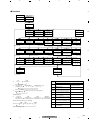
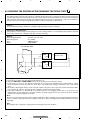
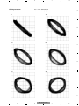
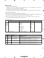
1
FORD
Service
Manual
ORDER NO.
CRT3094
DEH-2237ZF/X1R/UC
DISC PLAYER WITH AMPLIFIER
DEH-2237ZF
VEHICLE
Ranger
DESTINATION
U.S.A., CANADA
PRODUCED AFTER
August 2003
X1R/UC
FORD PART No.
ID No. PIONEER MODEL No.
FS-4L5T-18C868-AE
DEH-2237ZF/X1R/UC
- This service manual should be used together with the following manual(s):
Model No.
CX-977
Order No.
CRT2624
Mech. Module Remarks
S9
CD Mech. Module:Circuit Description, Mech.Description, Disassembly
For details, refer to "Important symbols for good services".
PIONEER CORPORATION
4-1, Meguro 1-Chome, Meguro-ku, Tokyo 153-8654, Japan
PIONEER ELECTRONICS (USA) INC. P.O.Box 1760, Long Beach, CA 90801-1760 U.S.A.
PIONEER EUROPE NV Haven 1087 Keetberglaan 1, 9120 Melsele, Belgium
PIONEER ELECTRONICS ASIACENTRE PTE.LTD. 253 Alexandra Road, #04-01, Singapore 159936
C PIONEER CORPORATION 2003
K-ZZD. JUNE 2003 Printed in Japan
1
A
2
3
4
[ Important symbols for good services ]
In this manual, the symbols shown-below indicate that adjustments, settings or cleaning should be made securely.
When you find the procedures bearing any of the symbols, be sure to fulfill them:
1. Product safety
You should conform to the regulations governing the product (safety, radio and noise, and other regulations), and
should keep the safety during servicing by following the safety instructions described in this manual.
2. Adjustments
To keep the original performances of the product, optimum adjustments or specification confirmation is indispensable.
In accordance with the procedures or instructions described in this manual, adjustments should be performed.
B
3. Cleaning
For optical pickups, tape-deck heads, lenses and mirrors used in projection monitors, and other parts requiring cleaning,
proper cleaning should be performed to restore their performances.
4. Shipping mode and shipping screws
To protect the product from damages or failures that may be caused during transit, the shipping mode should be set or
the shipping screws should be installed before shipping out in accordance with this manual, if necessary.
5. Lubricants, glues, and replacement parts
Appropriately applying grease or glue can maintain the product performances. But improper lubrication or applying
glue may lead to failures or troubles in the product. By following the instructions in this manual, be sure to apply the
prescribed grease or glue to proper portions by the appropriate amount.For replacement parts or tools, the prescribed
ones should be used.
C
- CD section precaution
D
1. Before disassembling the unit, be sure to turn off the
power. Unplugging and plugging the connectors during power-on mode may damage the ICs inside the
unit.
2. To protect the pickup unit from electrostatic discharge during servicing, take an appropriate treatment (shorting-solder) by referring to “the DISASSEMBLY” on page 46.
3. After replacing the pickup unit, be sure to check the
grating. (See p.40.)
SAFETY INFORMATION
E
This service manual is intended for qualified service technicians; it is not meant for the casual do-it-yourselfer.
Qualified technicians have the necessary test equipment and tools, and have been trained to properly and safely repair
complex products such as those covered by this manual.
Improperly performed repairs can adversely affect the safety and reliability of the product and may void the warranty.
If you are not qualified to perform the repair of this product properly and safely, you should not risk trying to do so
and refer the repair to a qualified service technician.
F
2
DEH-2237ZF/X1R/UC
1
2
3
4
5
6
7
8
CONTENTS
SAFETY INFORMATION ......................................................................................................................................................2
1. SPECIFICATIONS .................................................................................................................................................................4
2. EXPLODED VIEWS AND PARTS LIST ................................................................................................................................6
2.1 EXTERIOR ........................................................................................................................................................................6
2.2 CD MECHANISM MODULE ............................................................................................................................................8
3. BLOCK DIAGRAM AND SCHEMATIC DIAGRAM.............................................................................................................10
3.1 BLOCK DIAGRAM .........................................................................................................................................................10
3.2 OVERALL CONNECTION DIAGRAM(GUIDE PAGE) ...................................................................................................12
3.3 KEYBOARD UNIT ..........................................................................................................................................................18
3.4 CD MECHANISM MODULE ..........................................................................................................................................20
4. PCB CONNECTION DIAGRAM..........................................................................................................................................24
4.1 MOTHER UNIT ..............................................................................................................................................................24
4.2 KEYBOARD UNIT ..........................................................................................................................................................28
4.3 CD MECHANISM MODULE ..........................................................................................................................................30
5. ELECTRICAL PARTS LIST..................................................................................................................................................32
6. ADJUSTMENT ...................................................................................................................................................................38
6.1 CD ADJUSTMENT ........................................................................................................................................................38
6.2 CHECKING THE GRATING AFTER CHANGING THE PICKUP UNIT...........................................................................40
6.3 CD TEST MODE.............................................................................................................................................................42
7. GENERAL INFORMATION.................................................................................................................................................46
7.1 DIAGNOSIS ...................................................................................................................................................................46
7.1.1 DISASSEMBLY .......................................................................................................................................................46
7.1.2 CONNECTOR FUNCTION DESCRIPTION .............................................................................................................51
7.2 PARTS ............................................................................................................................................................................52
7.2.1 IC .............................................................................................................................................................................52
7.2.2 DISPLAY..................................................................................................................................................................56
7.3 OPERATIONAL FLOW CHART ......................................................................................................................................57
7.4 CLEANING .....................................................................................................................................................................58
8. OPERATIONS .....................................................................................................................................................................58
A
B
C
D
E
F
3
DEH-2237ZF/X1R/UC
5
6
7
8
1
A
2
3
4
1. SPECIFICATIONS
General
Power source ..............................................................................14.4V DC(10.5V-16.0V allowable)
Grounding system ......................................................................Negative type
Backup current ............................................................................3mA or less
Dimensions .................................................................................188(W) x100(H) x187(D)mm
Weight .........................................................................................2.0kg
B
CD player
System.........................................................................................Compact disc audio system
Usable discs ................................................................................Compact disc
Signal format ..............................................................................Sampling frequency : 44.1kHz
Number of quantization bits: 16;linear
S/N ...............................................................................................70dB or more
Distortion.....................................................................................0.1% or less
FM tuner
C
Frequency....................................................................................87.75, 87.9-107.9 MHz
S/N ...............................................................................................58dB or more
Distortion.....................................................................................1.0% or less
IF interference .............................................................................95dB or more
Image interference......................................................................45dB or more
Stereo Separation.......................................................................25dB or more(400Hz)
AM tuner
D
Frequency....................................................................................530-1710 kHz
S/N 20dB useable sensibility .....................................................33dBµ +4dB, -5dB
S/N ...............................................................................................50dB +10dB, -6dB
Distortion.....................................................................................1.5% or less
IF interference .............................................................................75dB or more
Image interference......................................................................60dB or more
E
F
4
DEH-2237ZF/X1R/UC
1
2
3
4
5
6
7
8
A
B
C
D
E
F
5
DEH-2237ZF/X1R/UC
5
6
7
8
1
2
3
4
2. EXPLODED VIEWS AND PARTS LIST
2.1 EXTERIOR
A
B
C
A
B
D
E
F
6
DEH-2237ZF/X1R/UC
1
2
3
4
6
5
8
7
NOTE:
A
- Parts marked by “*” are generally unavailable because they are not in our Master Spare Parts List.
- Screws adjacent to ∇ mark on the product are used for disassembly.
- For the applying amount of lubricants or glue, follow the instructions in this manual.
( In the case of no amount instructions, apply as you think it appropriate.)
- EXTERIOR SECTION PARTS LIST
Mark No. Description
1
2
3
4
5
*
*
Screw
Screw
Screw
CD Mechanism Module(S9V)
Part No.
Mark No. Description
Part No.
BMZ26P200FMC
BSZ26P060FMC
BSZ26P080FZK
CXK5525
41
42
43
44
45
Sheet
Connector
Connector
Housing
Knob Assy
HNM0103
HNV0049
HNV0050
HNV7069
HXA0385
•••••
6
7
8
9
10
Connector
Chassis
Case
Holder
Insulator
HDE0043
HNA0012
HNB0166
HNC0121
HNM0092
46
47
48
49
50
Grille Unit
Screw
Screw
Screw
Nut
HXA0420
IMS20P040FZK
IMS26P040FMC
ISS26P055FUC
NF50FMC
11
12
13
14
15
Seal
Insulator
Insulator
Heat Sink
Holder
HNM0115
HNM0116
HNM5230
HNR0242
HNV0048
51
52
53
54
Transistor(Q824)
Transistor(Q700)
Transistor(Q821)
Transistor(Q805)
KSA1220
KSD1273
2SB942A
KSB1366
16
17
18
19
20
Rail Guide
Mother Unit
Screw
FM/AM Tuner Unit
Holder
HNV6756
HWM0086
ASZ26P080FMC
CWE1561
CNC8855
21
22
23
24
25
Terminal(CN401,402)
IC(IC201)
Connector(CN607)
•••••
Connector(CN604)
CKF1059
TDA7384
CKS2251
26
27
28
29
30
Cushion
Plug(CN601)
Antenna Jack(CN602)
Holder
Holder
CNM6825
HKM1372
HKX1054
HNC0119
HNC0120
31
32
33
34
35
Holder
Chassis Unit
Screw
Cover
Rubber
HNC0125
HXA0379
BPZ26P080FMC
HNM7654
HNV7063
36
37
38
39
40
Keyboard Unit
LCD(LCD904)
Connector(CN901)
Lighting Conductor
Holder
HWM0087
CAW1822
CKS4576
CNV7936
HNC9816
B
C
D
CKS4575
E
F
7
DEH-2237ZF/X1R/UC
5
6
7
8
1
2
3
4
2.2 CD MECHANISM MODULE
A
B
C
GEM1040
GEM1035
GEM1035
D
E
C
F
8
DEH-2237ZF/X1R/UC
1
2
3
4
6
5
8
7
- CD MECHANISM MODULE SECTION PARTS LIST
Mark No. Description
Part No.
A
Mark No. Description
Part No.
CD Control Unit
Connector(CN701)
Connector(CN101)
Screw
Screw
CWX2701
CKS1959
CKS3486
BMZ20P025FTC
BSZ20P040FTC
46
47
48
49
50
Gear
Arm
Arm
Arm
Arm
CNV6320
CNV6322
CNV6323
CNV6324
CNV6888
6
7
8
9
10
Screw(M2x4)
Screw(M2x3)
Screw
Washer
Washer
CBA1362
CBA1527
CBA1545
CBF1037
CBF1038
51
52
53
54
55
Arm
Guide
Arm
Guide
Rack
CNV6889
CNV6327
CNV6924
CNV6921
CNV6923
11
12
13
14
15
Washer
Washer
Spring
Spring
Spring
CBF1039
CBF1060
CBH2378
CBH2379
CBH2514
56
57
58
59
60
Clamper
Arm
Guide
Cover
Arm
CNV6331
CNV6332
CNV6333
CNV6334
CNV6335
16
17
18
19
20
Spring
Spring
Spring
Spring
Spring
CBH2533
CBH2382
CBH2383
CBH2384
CBH2527
61
62
63
64
65
Guide
Roller
Damper
Damper
Guide
CNV6336
CNV6338
CNV6175
CNV6662
CNV6925
21
22
23
24
25
Spring
Spring
Spring
Spring
Spring
CBH2386
CBH2537
CBH2390
CBH2391
CBH2523
66
67
68
69
70
Chassis Unit
Arm Unit
Arm Unit
Arm Unit
Motor Unit(M2)
CXB7980
CXB7983
CXB7984
CXB7985
CXB5903
26
27
28
29
30
Spring
Spring
Spring
Spring
Shaft
CBH2426
CBH2444
CBL1561
CBL1553
CLA3845
71
72
73
74
75
Screw Unit
Gear Unit
Bracket Unit
Motor Unit(M1)
Arm Unit
CXB5904
CXB8076
CXB7982
CXB6007
CXB8504
31
32
33
34
35
Roller
Frame
Lever
Lever
Arm
CLA3910
CNC9654
CNC9664
CNC8949
CNC9661
76
77
78
79
80
Screw(M2x5)
Screw
Screw
Washer
Washer
EBA1028
JFZ20P020FTC
JGZ17P020FZK
YE15FTC
YE20FTC
36
37
38
39
40
Arm
Arm
Bracket
Frame
Belt
CNC9016
CNC9017
CNC9123
CNC8947
CNT1086
81
82
83
84
85
Pickup Unit(Service)(P9)
Screw
Guide
Roller
Spring
CXX1481
IMS26P030FTC
CNV6922
CNV6887
CBH2509
41
42
43
44
45
Gear
Gear
Gear
Gear
Gear
CNV6886
CNV6316
CNV6317
CNV6318
CNV6319
86
87
88
89
Spring
Spring
Collar
Damper
CBH2512
CBH2536
CNV6906
CNV6863
1
2
3
4
5
*
B
C
D
E
F
9
DEH-2237ZF/X1R/UC
5
6
7
8
1
2
3
4
3. BLOCK DIAGRAM AND SCHEMATIC DIAGRAM
3.1 BLOCK DIAGRAM
A
MOTHER UNIT
A
FM/AM TUNER UNIT
CN602
ANTENNA
JACK
1
FM/AM 1ST IF 10.7MHz
T51 Q51 CF51 CF52 CF53
AMRF
28
AMANT
MPXREF 41kHz
AMDET
ATT
L ch
IC 2 FM MPX
2
5
AMIN
ANT ADJ
FMANT
27
RFGND
26
Lch
6
R ch
COMP
IC1
MIXER, IF AMP, DET.
LDET
20
21
18
ATT
FMRF
CF202
PICKUP UNIT
(SERVICE)(S9)
MD
LOADING/ CARRIAGE
MOTOR
4
STIND
AMDET
NL2
FMSD
SL
SDBW
CE1
DGND
CK
CE2
NL1
3
1
9
LOCL
PDIO
2
15
8
5
LDO
RFRPIN
MDI
AC, F, E, BD
FOP
TOP
LD+
1
4
14
TU
CN607
CN701
FEO
24
38
16
43
14
46
TEO
IC 101
TA2153FN
FOP
TOP
IC 401
BA5996FM
V5
RFI
LO
FEI
XO
FD, TD, SD, MD
LOUT
85
14
14
LOUT
79
X301
TEI
SERVO
CONTROL,
DSP,
LPF, DAC
12
FOP
14
TOP
D
13
Q101
9
HOLOGRAM
UNIT
SPINDLE
MOTOR
8
XI
78
EC
XRST,XCE,XPCK,
IC 201
TC9495F2
XPI0-XPI3
XRST,XCE,XPCK,X0-X3
ACT,MOTOR
DRIVER
M
16
SOP
15
SOM
18
LCOM
17
LCOP
M
13
LOEJ
22
LOEJ
21
CLCONT
DSCSNS
HOME
CD5VON
10
10
15
15
17
17
16
16
1
1
LOEJ
84
CLCNT
78
DSCSNS
91
HOME
90
CD5V
80
VD
HOME
8EJ
VD
DSCSNS
2
2
VD
11
Q700
B.UP
V5
10
IC 701
2
IC 601(2/2)
PD5756A
rotint
CD5V
LOTIN0
SUBCLKO
SUBCLKI
VDCNT
wakeup
44
Q702
20 4
HOME
3 BLPWR
VDCONT
BA05SFP
5V REGULATOR
CLCNT
DSCSNC
LOTIN1
97
4
LOEJ
X602
Q701
1
71
XIN
SYSTEM CONTROLLER
VD REGULATOR
12EJ
FMUTE
15
CLCONT
CLAMP
XOUT
X601
76
77
73
ILMOUT
LD-
FOCUS ACT.
MONITOR TRACKING ACT.
DIODE
11 12 15 16
C CD CONTROL UNIT
CN101
LASER
DIODE
24
SWVDD
C
FMLOCL
22 10 19 14
SYS+B
VDD
Q401
VDD
CREQ
VCC
7 17
25
DI/DO
WC
AMPNS
RF ADJ
LOCL
LOCH
23
IC 3
EEPROM
AM 2ND IF X901
450kHz 10.25MHz
IMG ADJ
B
Q8
4
B.UP
Q822
E
ILMOUT
SWVDD
kdt)-kdt
LCDCE,lcdinh,
B.UP
Q827
F
BLPWR
10
DEH-2237ZF/X1R/UC
1
2
3
4
6
5
8
7
A
RESET
1
RESET
2
IC 801
VDD
S-80842CNDYI
SYS+B REGULATOR
VDD REGULATOR
Q808
12
reset
DIAGNOSTICS
Q805
VDD
B.UP
Q804
B.UP
SYS+B
Q873
Q807
PDO,PDI,PCK
epce,wc
SWVDD
VDD
Q874
Q806
Q691
SYSPW
SYSPWR
70
syspwr
Q852
SYSPW
Q840
SYSTEM CONTROLLER
bsens
IC 601(1/2)
PD5756A
B.UP
pck
Q870
pllce@
6
PWMIN
VDD
PDO
IC202 NJM2904V
Q321
Q325
Q323
1
Q327
CD L
4
LIN3-L
FL
IC 101
PML010A
RL
RLP
2
CN601
ACC
B.UP
ELECTRONIC VOLUME/
SOURCE SELECTOR
LIN1-L
FLP
IC203 NJM2904V
Q231
9
65
2
SWVDD
Q871
POWER AMP
IC301
6
5
10
FIX EQUALIZER
11
7
IC302
NJM2068V
11
5
7
15
FL-
IC 201
TDA7384
RL+
RLIN
RL-
MUTE
NJM2068V
6,20
FL+
FLIN
9
1
PDI
clipin
2
Q851
19
ilmint
PLLCE
1
TUNER L
A SENSE
Q872
ILL+
3
1
100
Q841
ILMIN
RL+
RL-
C
START
FL+
FL-
7
17
16
PDIO
95
ILMI
BACKUP
49
B
SYS+B
HARDMUTE
SD
97 SL
47 st
2
ACC
LOCL
18
46
B.UP
21
Q850
asens
48
B SENSE
27
19
8
IC 604
BR9010FV-W
STBY
22
4
SYSPW
Q329
ECLK,EDT,evce
Q201
FMUTE
FMUTE
71
Q202
HARDMUTE
D
IC 603
TC7S86F
rotint
LER
LOTIN0
LOTIN1
wakeup
2
20 4
1
76
77
73
CN604
Q906
CN901
Q901
VR901
ROTIN0
ROTIN1
Q821
18 ROTIN0
ROTIN0 2
19
19 ROTIN1
ROTIN1 1
27
27
KEYBOARD UNIT
KST5
4
CLK
Q902
KD2
Q692
WAKEUP
Q822
18
B
KD3
VDD
VOLUME/POWER
5
WAKEUP
KST5
WAKEUP
Q823
E
T
ILL+B
ILL+B
2
2
21
21 SWDVDD
ILLUMINATION
CD EJECT
Q809
Q904
KD0
VDD
SWVDD
D
KST5
Q810
kdt)-kdt$,kst)-kst%
KEY MATRIX
kdt)-kdt$,kst)-kst%
93
VDD
LCDCE,lcdinh,LCDCLK,LCDDT
LCDCE,lcdinh,LCDCLK,LCDDT
LCD DRIVER
Q824
P
IC 901
LC75813E
Q827
Q825
Q826
BL+B
1
1
LCD 904
LCD BACKLIGHT
BL+B
F
WR
11
DEH-2237ZF/X1R/UC
5
6
7
8
1
2
3
4
3.2 OVERALL CONNECTION DIAGRAM(GUIDE PAGE)
Note: When ordering service parts, be sure to refer to " EXPLODED VIEWS AND PARTS LIST" or
"ELECTRICAL PARTS LIST".
A-a
A
A-a
A-b
Large size
SCH diagram
FM/AM TUNER UNIT
A-a
A-a
A-b
A-b
FM:-25.0dBs(100%,400Hz,MONO)
AM:-25.0dBs(30% Mod.,400Hz,MONO)
Guide page
FM:-35.47dBs
AM:-35.47dBs
CD: -1.97dBs
Detailed page
ELECTRONIC VOLUME
SOURCE SELECTOR
B
C
SYSTEM CONTROLLER
D
C
CN701
CD:+1.10dBs(1kHz,0dB)
E
F
B
A
12
CN901
DEH-2237ZF/X1R/UC
1
2
3
4
5
6
8
7
A-b
A
A
MOTHER UNIT
FM: +4.63dBs
AM: +5.63dBs
CD:+23.13dBs
TRONIC VOLUME/
FM:-21.37dBs
URCE SELECTOR
AM:-20.37dBs
CD: -2.87dBs
B
C
OLLER
NC(PTA)
NC(PHONE INPUT +)
NC(PHONE INPUT -)
NC(PHONE SHIELD)
D
E
NOTE :
Symbol indicates a resistor.
No differentiation is made between chip resistors and
discrete resistors.
Symbol indicates a capacitor.
No differentiation is made between chip capacitors and
discrete capacitors.
Decimal points for resistor
and capacitor fixed values
are expressed as :
2.2 ← 2R2
0.022 ← R022
NC(PTA)
NC(PHONE INPUT +)
NC(PHONE INPUT -)
NC(PHONE SHIELD)
F
A
13
DEH-2237ZF/X1R/UC
5
6
7
8
E
FM/AM TUNER UNIT
D
FM:-25.0dBs(100%,400Hz,MONO)
AM:-25.0dBs(30% Mod.,400Hz,MONO)
A-a A-b
A-b
1
1
A
ELECTRONIC VOLUME/
FM:-21.37dBs
SOURCE SELECTOR
AM:-20.37dBs
CD: -2.87dBs
2
14
2
SYSTEM CONTROLLER
FM:-35.47dBs
AM:-35.47dBs
CD: -1.97dBs
1
2
3
3
4
3
B
C
F
A-a
DEH-2237ZF/X1R/UC
4
6
5
7
A-b
5
4
8
SYSTEM CONTROLLER
A
B
CN901
B
A-a A-b
C
D
E
C
CD:+1.10dBs(1kHz,0dB)
CN701
F
A-a
15
DEH-2237ZF/X1R/UC
5
6
7
8
A
A-b
1
1
NC(PTA)
FM: +4.63dBs
AM: +5.63dBs
CD:+23.13dBs
MOTHER UNIT
A
2
FM:-21.37dBs
AM:-20.37dBs
CD: -2.87dBs
A-a A-b
1
2
16
2
3
3
4
B
C
D
E
F
3
DEH-2237ZF/X1R/UC
4
5
Decimal points for resistor
and capacitor fixed values
are expressed as :
2.2 ← 2R2
0.022 ← R022
NC(PTA)
NC(PHONE INPUT +)
NC(PHONE INPUT -)
NC(PHONE SHIELD)
6
4
6
7
5
7
A-a A-b
NOTE :
Symbol indicates a resistor.
No differentiation is made between chip resistors and
discrete resistors.
Symbol indicates a capacitor.
No differentiation is made between chip capacitors and
discrete capacitors.
NC(PHONE SHIELD)
NC(PHONE INPUT -)
NC(PHONE INPUT +)
NC(PTA)
5
8
A
B
C
D
E
F
A-b
DEH-2237ZF/X1R/UC
8
17
1
2
3
4
3
4
3.3 KEYBOARD UNIT
A
B
(KL)
(KL)
C
D
E
105mA, 8V
F
A
B
18
CN604
DEH-2237ZF/X1R/UC
1
2
5
6
8
7
B
A
KEYBOARD UNIT
VOLUME/POWER
POWER
B
CLK
C
CD EJECT
SEEK DOWN
SEEK UP
D
TUNE DOWN
TUNE UP
MUTE
E
F
B
19
DEH-2237ZF/X1R/UC
5
6
7
8
1
2
3
4
3.4 CD MECHANISM MODULE
A
PICKUP UNIT(SERVICE)(S9)
F
F
T
F
T
B
F
T
T
F
T
91K
T
91K
%
F
T
T
T
F
F
*
F
F
T
8
0
F
RF AMP
T
C
S
C
&
MOTOR DRIVER LOGIC TABLE
D
ACT/MOTOR DRIVER
7
S
!
T
5
F
C
S
S
C
T
C
E
F
F
^
T
S
C
C
LOADING/CARRIAGE MOTOR
M2 CXB5903
5V
REGULATOR
F
C
20
DEH-2237ZF/X1R/UC
1
2
3
4
S
SPINDLE MOTOR
M1 CXB6007
(
6
5
8
7
C CD CONTROL UNIT
A
#
$ @
B
SERVO CONTROL/DSP/DAC/LPF
)
21
C
&
9
S
16.934MHz
6
A
CN607
F
T
C
S
(
SIGNAL LINE
FOCUS SERVO LINE
TRACKING SERVO LINE
CARRIAGE SERVO LINE
SPINDLE SERVO LINE
D
4
3
SWITCHES:
CONTROL UNIT
S901 : HOME SWITCH.....ON-OFF
S902 : CLAMP SWITCH....ON-OFF
S903 : DSCSNS SWITCH....ON-OFF
S904 : 12EJ SWITCH....ON-OFF
S905 : 8EJ SWITCH....ON-OFF
The underlined indicates the switch position.
2
1
E
F
C
DEH-2237ZF/X1R/UC
5
6
7
8
21
1
2
3
4
Note:1. The encircled numbers denote measuring pointes in the circuit diagram.
2. Reference voltage
VREF:2.1V
A
- Waveforms
1
2
3
4
B
1
2
3
4
CH1:DSCSNS 5V/div.
CH2:CLCONT 5V/div.
500ms/div.
CH3:LOEJ
5V/div.
CH4:VD1
10V/div.
When loading (12 cm CD)
5 CH1:FD
500mV/div.
CH1:DSCSNS 5V/div.
6 CH2:FOK
5V/div.
500ms/div.
CH2:CLCONT 5V/div.
500ms/div.
7 CH3:MD
5V/div.
CH3:LOEJ
5V/div.
CH4:VD1
10V/div.
When setting up "Source On"
When loading (8 cm CD)
Ref. :
GND
Ref. :
GND
Ref. :
VREF
Mode :
Normal
Mode :
Normal
Mode :
Normal
5 CH1:FD
6 CH2:FOK
7 CH3:MD
8 CH1:FE
500mV/div.
500ms/div.
9 CH2:FOON 5V/div.
500mV/div.
5V/div.
100ms/div.
5V/div.
When setting up "Source On"
0 CH1:TE
8 CH2:FE
500mV/div.
200ms/div.
500mV/div.
When setting up "Source On"
Magnified drawing for "time"
C
Ref. :
VREF
Ref. :
VREF
Ref. :
VREF
Mode :
Normal
Mode :
Normal
Mode :
Normal
8
5
0
!
D
CH1:FE
500mV/div.
CH2:FD
500mV/div.
CH3:TE
500mV/div.
CH4:TD
500mV/div.
During "Play"
@ CH1:BCK
1ms/div.
2V/div.
1µs/div. # CH1:LRCK 2V/div.
$ CH2:DOUT 2V/div.
During "Play"
During "Play"
Ref. :
VREF
Ref. :
VREF
Ref. :
VREF
Mode :
Normal
Mode :
Normal
Mode :
Normal
7 CH1:MD
500mV/div.
500mV/div.
500mV/div. 0.5µs/div. % CH1:RFO
0 CH2:TE
500mV/div.
During "Play"
During "Tracking Open"
10µs/div. % CH1:RFO
E
During "Play"
Ref. :
VREF
Ref. :
VREF
Ref. :
VREF
Mode :
Normal
Mode :
Normal
Mode :
Test
F
22
DEH-2237ZF/X1R/UC
1
10µs/div.
2
3
4
2ms/div.
6
5
8
7
A
5 CH1:FD
^ CH2:FOP
1V/div.
2V/div.
200ms/div.
% CH1:RFO
0 CH2:TE
! CH3:TD
With no disk inserted
During "Focus Close"
% CH1:RFO
1V/div.
500mV/div. 500µs/div. 0 CH2:TE
! CH3:TD
1V/div.
Ref. :
VREF
Ref. :
VREF
Mode :
Test
Mode :
Test
Mode :
Test
1V/div.
1V/div.
1V/div.
%
5ms/div. &
5
!
100 Track Jump
CH1:RFO
CH2:DFCT
CH3:FD
CH4:TD
2V/div.
5V/div.
1V/div.
2V/div.
% CH1:RFO
500µs/div. 0 CH2:TE
& CH3:DFCT
When reproducing black dots (800µm)
Ref. :
VREF
Ref. :
VREF
Mode :
Test
Mode :
Normal
Mode :
Normal
500mV/div. 200ms/div.
2V/div.
1 CH1:DSCSNS
2 CH2:CLCONT
3 CH3:LOEJ
B
1V/div.
500mV/div. 200ms/div.
5V/div.
During inside/outside search
Ref. :
VREF
* CH1:TEY
( CH2:SD
5ms/div.
32 Track Jump
1 Track Jump
Ref. :
VREF
% CH1:RFO
0 CH2:TE
! CH3:TD
1V/div.
1V/div.
1V/div.
1 CH1:DSCSNS
5V/div.
5V/div. 200ms/div. 2 CH2:CLCONT
3 CH3:LOEJ
5V/div.
C
5V/div.
5V/div. 200ms/div.
5V/div.
During inside/outside search
When "Eject" (8cm CD)
When "Eject" (12 cm CD)
Ref. :
VREF
Ref. :
GND
Ref. :
GND
Mode :
Normal
Mode :
Normal
Mode :
Normal
) CH1:LOUT 2V/div.
⁄ CH2:ROUT 2V/div.
D
200µs/div.
E
"Play" in 1kHz, 0dB
Ref. :
GND
Mode :
Normal
F
23
DEH-2237ZF/X1R/UC
5
6
7
8
1
2
3
4
4. PCB CONNECTION DIAGRAM
4.1 MOTHER UNIT
A
NOTE FOR PCB DIAGRAMS
1.The parts mounted on this PCB
include all necessary parts for
several destination.
For further information for
respective destinations, be sure
to check with the schematic diagram.
2.Viewpoint of PCB diagrams
Connector
A
MOTHER UNIT
Capacitor
CAR HARNESS
1
SIDE A
9
Chip Part
3
4
5
6
7
8
J1
B
P.C.Board
2
10
11
12
J3
13
14
15
16
10
11
12
13
SIDE B
C
D
E
F
FRONT
A
24
DEH-2237ZF/X1R/UC
1
2
3
4
5
6
8
7
A
SIDE A
ANTENNA
2
FM/AM TUNER UNIT
3
1
B
C
D
C
E
CN701
F
B
T
CN901
A
25
DEH-2237ZF/X1R/UC
5
6
7
8
1
2
3
4
3
4
A
A
MOTHER UNIT
1
B
C
D
E
F
A
26
DEH-2237ZF/X1R/UC
1
2
5
6
7
8
A
SIDE B
1
B
C
D
E
F
A
27
DEH-2237ZF/X1R/UC
5
6
7
8
F
1
28
2
SCAN
2
SEEK UP
D
3
AM
FM
4
TAPE
EJECT
5
TUNE
DOWN
MENU
6
TUNE UP
2
1
SEEK DOWN
MUTE
CLK
A
CD EJECT
B
VOLUME/POWER
CD
1
3
3
4
4.2 KEYBOARD UNIT
KEYBOARD UNIT
SIDE A
B
LCD904
C
E
B
DEH-2237ZF/X1R/UC
4
5
B
6
8
7
KEYBOARD UNIT
SIDE B
A
B
C
A
CN604
D
E
F
B
29
DEH-2237ZF/X1R/UC
5
6
7
8
1
2
3
4
4.3 CD MECHANISM MODULE
C
A
SIDE A
CD CONTROL UNIT
12EJ
DSCSNS
M2
LOADING
/CARRIAGE
MOTOR
B
M1
SPINDLE
MOTOR
C
A
CN607
D
HOME
PICKUP UNIT
(SERVICE)(P9)
VREF2
E
F
E
F
C
30
DEH-2237ZF/X1R/UC
1
2
3
4
6
5
C
8
7
SIDE B
CD CONTROL UNIT
A
8EJ
CLAMP
B
C
D
E
F
C
31
DEH-2237ZF/X1R/UC
5
6
7
8
1
A
2
3
4
5. ELECTRICAL PARTS LIST
NOTES:
- Parts whose parts numbers are omitted are subject to being not supplied.
- The part numbers shown below indicate chip components.
Chip Resistor
RS1/_S___J,RS1/__S___J
Chip Capacitor (except for CQS.....)
CKS....., CCS....., CSZS.....
B
=====Circuit Symbol and No.===Part Name
--- -----------------------------------------------
A
Part No.
-------------------------
Unit Number : HWM0086
Unit Name
: Mother Unit
MISCELLANEOUS
C
D
E
F
IC
IC
IC
IC
IC
101
201
202
203
301
IC
IC
IC
IC
IC
PML010A
TDA7384
NJM2904V
NJM2904V
NJM2068V
IC
IC
IC
IC
IC
302
601
603
604
801
IC
IC
IC
IC
IC
NJM2068V
PD5756A
TC7S86F
BR9010FV-W
S-80842CNDYI
Q
Q
Q
Q
Q
201
202
231
321
322
Transistor
Transistor
Transistor
Transistor
Transistor
DTC124EU
DTC124EU
DTC114EU
2SC4081
2SC4081
Q
Q
Q
Q
Q
323
324
325
326
327
Transistor
Transistor
Transistor
Transistor
Transistor
2SC4081
2SC4081
2SC4081
2SC4081
2SC4081
Q
Q
Q
Q
Q
328
329
330
410
691
Transistor
Transistor
Transistor
Transistor
Transistor
2SC4081
2SC4081
2SC4081
2SC4081
DTA114EU
Q
Q
Q
Q
Q
692
700
701
702
804
Transistor
Transistor
Transistor
Transistor
Transistor
DTC124EU
KSD1273
2SA1576
DTC114EU
2SB1236
Q
Q
Q
Q
Q
805
806
807
808
809
Transistor
Transistor
Transistor
Transistor
Transistor
KSB1366
IMX1
2SC4081
2SD2318F5
2SA1576
Q
Q
Q
Q
Q
810
821
822
823
824
Transistor
Transistor
Transistor
Transistor
Transistor
DTC114EU
2SB942A
2SC4081
2SC4081
KSA1220
Q
Q
Q
Q
Q
825
826
827
840
841
Transistor
Transistor
Transistor
Transistor
Transistor
2SC4081
2SC4081
2SA1576
2SC4081
2SC4081
Q
Q
Q
Q
Q
850
851
852
870
871
Transistor
Transistor
Transistor
Transistor
Transistor
DTA144EU
2SC4081
2SC4081
DTA124EU
2SC4081
32
=====Circuit Symbol and No.===Part Name
--- -----------------------------------------------
Part No.
-------------------------
Q
Q
Q
D
D
872
873
874
201
202
Transistor
Transistor
Transistor
Diode
Diode
2SC4081
2SA1576
DTC114EU
DAN202U
DAN202U
D
D
D
D
D
700
801
802
805
806
Diode
Diode
Diode
Diode
Diode
HZS9L(B1)
RM4Z-LFJ4
ERA15-02VH
HZS9L(A1)
ERA15-02VH
D
D
D
D
D
807
830
840
841
850
Diode
Diode
Diode
Diode
Diode
HZS6L(B2)
1SS355
HZS7L(C2)
HZS9L(A2)
UDZS5R6(B)
D
D
D
D
D
851
852
873
874
875
Diode
Diode
Diode
Diode
Diode
DAN202U
HZS9L(B2)
HZS12L(C1)
1SS133
MA732
L
L
L
L
L
101
410
411
412
413
Inductor
Ferri-Inductor
Coil
Inductor
Inductor
LAU2R2K
LAU4R7K
CTB1103
LAU2R2K
LAU2R2K
L
L
L
L
L
601
603
604
616
620
Inductor
Inductor
Inductor
Inductor
Inductor
LCTA2R2J2520
HTF0002
HTF0002
HTF0002
HTF0002
L
TH
X
X
EF
801
601
601
602
801
Choke Coil 600µH
Thermistor
Radiator 16.000MHz
Radiator 32.768kHz
EMI Filter
CTH1243
CCX1032
CSS1571
CSS1319
HCG0001
AR
410
Surge Protector
FM/AM Tuner Unit
DSP-201M-S00B
CWE1561
RESISTORS
R
R
R
R
R
117
118
121
122
123
RS1/16S682J
RS1/16S682J
RS1/16S0R0J
RS1/16S0R0J
RS1/16S302J
R
R
R
R
R
124
125
126
201
202
RS1/16S302J
RS1/16S132J
RS1/16S132J
RS1/16S103J
RS1/16S221J
R
R
R
R
R
203
204
205
206
231
RS1/16S153J
RS1/16S101J
RS1/16S103J
RS1/16S0R0J
RS1/16S103J
DEH-2237ZF/X1R/UC
1
2
3
4
5
6
7
8
=====Circuit Symbol and No.===Part Name
--- -----------------------------------------------
Part No.
-------------------------
=====Circuit Symbol and No.===Part Name
--- -----------------------------------------------
Part No.
-------------------------
R
R
R
R
R
232
233
234
235
236
RS1/16S103J
RS1/16S103J
RS1/16S103J
RS1/16S103J
RS1/16S103J
R
R
R
R
R
418
419
420
421
422
RS1/16S472J
RS1/16S473J
RS1/16S681J
RS1/16S473J
RS1/16S473J
R
R
R
R
R
237
238
239
245
281
RS1/16S103J
RS1/16S103J
RAB4C682J
RAB4C821J
RS1/16S0R0J
R
R
R
R
R
423
424
425
426
427
RS1/16S473J
RS1/16S681J
RS1/16S681J
RS1/16S103J
RS1/16S393J
R
R
R
R
R
282
311
312
315
316
RS1/16S0R0J
RS1/16S0R0J
RS1/16S0R0J
RS1/16S0R0J
RS1/16S0R0J
R
R
R
R
R
430
601
602
603
604
RS1/16S563J
RS1/16S471J
RS1/16S102J
RAB4C102J
RS1/16S473J
R
R
R
R
R
321
322
325
326
327
RS1/16S512J
RS1/16S512J
RS1/16S822J
RS1/16S822J
RS1/16S122J
R
R
R
R
R
605
606
612
614
615
RS1/16S471J
RS1/16S102J
RS1/16S473J
RS1/16S102J
RS1/16S102J
R
R
R
R
R
328
329
330
331
332
RS1/16S122J
RS1/16S683J
RS1/16S683J
RS1/16S472J
RS1/16S472J
R
R
R
R
R
616
619
620
621
622
RS1/16S471J
RS1/16S0R0J
RS1/16S471J
RAB4C102J
RS1/16S0R0J
R
R
R
R
R
333
334
337
338
339
RS1/16S562J
RS1/16S562J
RS1/16S122J
RS1/16S122J
RS1/16S683J
R
R
R
R
R
624
626
628
629
631
RS1/16S0R0J
RS1/16S102J
RAB4C0R0J
RAB4C102J
RS1/16S473J
R
R
R
R
R
340
341
342
343
344
RS1/16S683J
RS1/16S472J
RS1/16S472J
RS1/16S0R0J
RS1/16S0R0J
R
R
R
R
R
633
634
636
637
638
RS1/16S0R0J
RS1/16S471J
RS1/16S0R0J
RS1/16S102J
RS1/16S102J
R
R
R
R
R
347
348
349
350
351
RS1/16S122J
RS1/16S122J
RS1/16S683J
RS1/16S683J
RS1/16S472J
R
R
R
R
R
640
644
646
647
649
RS1/16S472J
RAB4C471J
RS1/16S102J
RS1/16S102J
RAB4C102J
R
R
R
R
R
352
355
356
357
358
RS1/16S472J
RS1/16S272J
RS1/16S272J
RS1/16S122J
RS1/16S122J
R
R
R
R
R
650
651
652
653
655
RS1/16S102J
RAB4C103J
RS1/16S473J
RS1/16S102J
RS1/16S333J
R
R
R
R
R
359
360
361
362
363
RS1/16S683J
RS1/16S683J
RS1/16S472J
RS1/16S472J
RS1/16S512J
R
R
R
R
R
656
657
658
661
662
RS1/16S471J
RS1/16S102J
RS1/16S101J
RS1/16S0R0J
RS1/16S102J
R
R
R
R
R
364
367
368
369
370
RS1/16S512J
RS1/16S512J
RS1/16S512J
RS1/16S182J
RS1/16S182J
R
R
R
R
R
663
664
665
666
668
RS1/16S0R0J
RAB4C222J
RS1/16S303J
RAB4C102J
RS1/16S473J
R
R
R
R
R
373
374
375
376
377
RS1/16S122J
RS1/16S122J
RS1/16S683J
RS1/16S683J
RS1/16S472J
R
R
R
R
R
674
675
676
677
678
RS1/16S184J
RS1/16S103J
RS1/16S103J
RS1/16S222J
RS1/16S222J
R
R
R
R
R
378
389
390
410
412
RS1/16S472J
RS1/16S512J
RS1/16S512J
RS1/16S222J
RS1/16S222J
R
R
R
R
R
679
697
698
699
700
RS1/16S104J
RAB4C102J
RS1/16S473J
RS1/16S473J
RS1/16S223J
R
R
R
R
R
413
414
415
416
417
RS1/16S473J
RS1/16S681J
RS1/16S681J
RS1/16S681J
RS1/16S473J
R
R
R
R
R
701
702
703
704
705
RS1/16S103J
RD1/4PU331J
RS1/16S103J
RS1/16S103J
RS1/16S0R0J
A
B
C
D
E
33
DEH-2237ZF/X1R/UC
5
6
F
7
8
1
A
2
3
4
=====Circuit Symbol and No.===Part Name
--- -----------------------------------------------
Part No.
-------------------------
=====Circuit Symbol and No.===Part Name
--- -----------------------------------------------
Part No.
-------------------------
R
R
R
R
R
721
722
751
801
807
RS1/16S272J
RS1/16S272J
RD1/4PU0R0J
RD1/4PU102J
RS1/16S472J
C
C
C
C
C
125
126
129
130
201
CKSRYB272K50
CKSRYB272K50
CKSRYB104K16
CKSRYB104K16
CEJQ330M10
R
R
R
R
R
809
810
811
812
813
RD1/4PU331J
RS1/16S272J
RS1/16S103J
RS1/16S332J
RS1/16S132J
C
C
C
C
C
202
203
204
205
211
CEJQ010M50
CFTLA105J50
CEJQ100M16
CKSRYF104Z25
CFTNA224J50
R
R
R
R
R
814
815
816
817
818
RD1/4PU271J
RS1/16S471J
RS1/16S222J
RD1/4PU102J
RS1/16S103J
C
C
C
C
C
212
213
214
221
222
CFTNA224J50
CFTNA224J50
CFTNA224J50
CKSRYB102K50
CKSRYB102K50
R
R
R
R
R
819
820
821
822
823
RS1/16S105J
RS1/16S221J
RS1/16S222J
RS1/16S222J
RS1/16S221J
C
C
C
C
C
223
224
225
226
227
CKSRYB102K50
CKSRYB102K50
CKSRYB102K50
CKSRYB102K50
CKSRYB102K50
R
R
R
R
R
824
825
826
827
828
RS1/16S471J
RS1/16S105J
RS1/16S222J
RS1/16S331J
RS1/16S152J
C
C
C
C
C
228
302
303
311
312
CKSRYB102K50
CKSRYB104K25
CKSRYB104K25
CEJQ100M16
CEJQ100M16
R
R
R
R
R
829
830
831
833
834
RS1/16S331J
RS1/16S102J
RS1/16S822J
RD1/4PU1R8J
RS1/16S102J
C
C
C
C
C
315
316
321
322
323
CEJQ100M16
CEJQ100M16
CKSRYB474K10
CKSRYB474K10
CKSRYB154K10
R
R
R
R
R
841
842
843
844
845
RS1/16S473J
RS1/16S473J
RS1/16S473J
RS1/16S473J
RS1/16S473J
C
C
C
C
C
324
325
326
327
328
CKSRYB154K10
CKSRYB104K16
CKSRYB104K16
CKSRYB393K25
CKSRYB393K25
R
R
R
R
R
846
850
851
852
853
RS1/16S473J
RS1/16S472J
RS1/16S472J
RD1/4PU102J
RS1/16S472J
C
C
C
C
C
329
330
331
332
333
CKSRYB103K50
CKSRYB103K50
CKSRYB153K25
CKSRYB153K25
CKSRYB103K50
R
R
R
R
R
854
855
870
871
872
RS1/16S102J
RS1/16S472J
RD1/4PU102J
RS1/16S0R0J
RS1/16S104J
C
C
C
C
C
334
335
336
337
338
CKSRYB103K50
CKSRYB392K50
CKSRYB392K50
CCSRCH121J50
CCSRCH121J50
R
R
R
R
R
873
874
875
876
877
RS1/16S472J
RS1/16S473J
RS1/16S473J
RS1/16S473J
RS1/16S473J
C
C
C
C
C
367
368
369
370
375
CKSRYB474K10
CKSRYB474K10
CKSRYB153K25
CKSRYB153K25
CCSRCH121J50
R
R
R
R
R
878
879
880
883
891
RS1/16S0R0J
RS1/16S472J
RS1/16S473J
RD1/4PU331J
RS1/16S152J
C
C
C
C
C
376
410
411
413
414
CCSRCH121J50
CKSQYB103K50
CKSRYB103K50
CKSRYB103K50
CEJQ220M10
R
R
R
R
892
893
895
896
RS1/16S152J
RS1/16S0R0J
RS1/16S103J
RS1/16S103J
C
C
C
C
C
417
418
419
420
421
CEJQ101M6R3
CKSRYB103K50
CKSRYB183K50
CKSRYB183K50
CKSRYB472K50
C
C
C
C
C
423
424
601
602
603
CKSRYB682K50
CKSRYB392K50
CCSRCH220J50
CCSRCH180J50
CEJQ100M16
C
C
C
C
C
604
607
608
630
658
CCSRCH101J50
CCSRCH220J50
CCSRCH220J50
CKSRYB102K50
CKSRYB104K25
B
C
D
E
CAPACITORS
F
C
C
C
C
C
101
102
103
104
115
CKSRYB104K25
CEJQ470M10
CEJQ100M16
CKSRYB104K25
CKSRYB474K10
C
C
C
C
C
116
117
118
119
120
CKSRYB474K10
CKSRYB474K10
CKSRYB474K10
CKSRYB474K10
CKSRYB474K10
34
DEH-2237ZF/X1R/UC
1
2
3
4
5
6
7
8
=====Circuit Symbol and No.===Part Name
--- -----------------------------------------------
Part No.
-------------------------
=====Circuit Symbol and No.===Part Name
--- -----------------------------------------------
Part No.
-------------------------
C
C
C
C
C
661
662
692
700
701
CKSRYB681K50
CKSRYB681K50
CKSRYB104K25
CKSRYB102K50
CKSRYB473K50
D
D
D
D
D
941
942
943
944
945
Chip LED
Chip LED
LED
LED
LED
SML010PT(KL)
SML010PT(KL)
SML-310PT(KL)
SML-310PT(KL)
SML-310PT(KL)
C
C
C
C
C
702
705
706
731
801
CEJQ101M10
CEJQ100M16
CEJQ100M16
CEJQ101M16
HCH0015
D
D
D
D
D
946
947
948
951
953
LED
LED
LED
Diode
Diode
SML-310PT(KL)
SML-310PT(KL)
SML-310PT(KL)
DAN202U(KL)
1SS355
C
C
C
C
C
803
804
805
807
808
CKSRYB223K50
CEJQ100M16
CKSRYB102K50
CEJQ220M10
CKSRYB473K50
D
D
D
L
IL
954
955
956
900
901
Diode
Diode
Diode
Inductor
Lamp 8V 105mA
1SS355
1SS355
1SS355
LCTB2R2K1608
CEL1747
C
C
C
C
C
809
810
820
821
822
CCH1149
CKSRYB103K50
CEJQ101M10
CKSRYB472K50
CKSRYB223K50
IL
902
VR 901
LCD 904
Lamp 8V 105mA
Encoder(VOLUME/POWER)
LCD
CEL1747
CSD1073
CAW1822
C
C
C
C
C
823
824
830
850
851
CEJQ100M16
CKSRYB102K50
CEJQ2R2M50
CKSRYB221K50
CKSRYB102K50
R
R
R
R
R
901
902
903
904
905
RS1/16S473J
RS1/16S472J
RS1/16S472J
RS1/16S472J
RS1/16S471J
C
C
C
C
C
870
871
872
873
880
CCSRCH181J50
CKSRYB102K50
CKSRYB102K50
CKSRYB473K50
CKSRYB472K50
R
R
R
R
R
906
907
908
921
922
RS1/16S471J
RS1/16S471J
RS1/16S471J
RS1/16S181J
RS1/16S181J
R
R
R
R
R
923
924
925
926
927
RS1/16S181J
RS1/16S181J
RS1/16S181J
RS1/16S181J
RS1/16S181J
R
R
R
R
R
928
929
930
931
932
RS1/16S181J
RS1/16S181J
RS1/16S181J
RS1/16S181J
RS1/16S181J
R
R
R
R
R
933
934
935
936
937
RS1/16S181J
RS1/16S181J
RS1/16S181J
RS1/16S181J
RS1/16S181J
R
R
R
R
R
938
939
940
941
942
RS1/16S181J
RS1/16S181J
RS1/16S181J
RS1/16S181J
RS1/16S181J
R
R
R
R
R
943
944
945
946
947
RS1/16S181J
RS1/16S181J
RS1/16S181J
RS1/16S181J
RS1/16S181J
R
R
R
R
R
948
949
950
951
952
RS1/16S181J
RS1/16S181J
RS1/16S181J
RS1/16S151J
RS1/16S151J
R
R
R
R
R
953
954
955
956
957
RS1/16S181J
RS1/16S181J
RS1/16S181J
RS1/16S181J
RS1/16S181J
R
958
RS1/16S181J
4700µF/16V
A
B
B
1000µF/16V
Unit Number : HWM0087
Unit Name
: Keyboard Unit
MISCELLANEOUS
IC
Q
Q
Q
Q
901
901
902
904
906
IC
Transistor
Transistor
Transistor
Transistor
LC75813E
DTC114EU
DTC114EU
DTC114EU
DTA114EU
D
D
D
D
D
911
912
913
914
915
LED
LED
LED
LED
LED
SML-310PT(KL)
SML-310PT(KL)
SML-310PT(KL)
SML-310PT(KL)
SML-310PT(KL)
D
D
D
D
D
916
917
918
919
920
LED
LED
LED
LED
LED
SML-310PT(KL)
SML-310PT(KL)
SML-310PT(KL)
SML-310PT(KL)
SML-310PT(KL)
D
D
D
D
D
921
922
923
924
925
LED
LED
LED
LED
LED
SML-310PT(KL)
SML-310PT(KL)
SML-310PT(KL)
SML-310PT(KL)
SML-310PT(KL)
D
D
D
D
D
926
927
928
929
930
LED
LED
LED
LED
LED
SML-310PT(KL)
SML-310PT(KL)
SML-310PT(KL)
SML-310PT(KL)
SML-310PT(KL)
D
D
D
D
D
931
932
933
934
935
LED
LED
LED
LED
LED
SML-310PT(KL)
SML-310PT(KL)
SML-310PT(KL)
SML-310PT(KL)
SML-310PT(KL)
D
D
D
D
D
936
937
938
939
940
LED
LED
LED
LED
LED
SML-310PT(KL)
SML-310PT(KL)
SML-310PT(KL)
SML-310PT(KL)
SML-310PT(KL)
RESISTORS
6
D
E
F
35
DEH-2237ZF/X1R/UC
5
C
7
8
1
2
=====Circuit Symbol and No.===Part Name
--- -----------------------------------------------
A
3
Part No.
-------------------------
CAPACITORS
C
C
C
C
C
C
901
902
903
904
905
CKSRYB104K16
CCSRCH681J50
CKSRYB104K16
CKSRYB104K16
CKSRYB104K25
Unit Number : CWX2701
Unit Name
: CD Control Unit
MISCELLANEOUS
B
C
IC
IC
IC
IC
Q
101
201
401
701
101
IC
IC
IC
IC
Transistor
TA2153FN
TC9495F2
BA5996FM
BA05SFP
2SD1664
Q
L
L
L
L
102
301
302
303
304
Transistor
Inductor
Inductor
Inductor
Inductor
UMD2N
CTF1546
CTF1546
CTF1546
CTF1546
L
L
L
L
L
305
306
307
308
701
Inductor
Inductor
Inductor
Inductor
Inductor
CTF1546
CTF1546
CTF1546
CTF1546
CTF1546
L
L
L
L
L
702
703
704
705
706
Inductor
Inductor
Inductor
Inductor
Inductor
CTF1546
CTF1546
CTF1546
CTF1546
CTF1546
L
X
S
S
S
707
301
901
902
903
Inductor
Ceramic Resonator 16.934MHz
Switch(HOME)
Spring Switch(CLAMP)
Switch(DSCSNS)
CTF1546
CSS1525
CSN1051
CSN1052
CSN1051
S
S
EF
904
905
701
Spring Switch(12EJ)
Switch(8EJ)
Emi Filter
CSN1052
CSN1051
CCG1051
E
=====Circuit Symbol and No.===Part Name
--- -----------------------------------------------
Part No.
-------------------------
R
R
R
R
R
321
323
401
402
403
RS1/16S331J
RS1/16S332J
RS1/16S684J
RS1/16S103J
RS1/16S103J
R
R
R
R
R
404
405
407
408
409
RS1/16S183J
RS1/16S123J
RS1/16S622J
RS1/16S622J
RS1/16S113J
R
R
R
R
R
410
701
702
703
704
RS1/16S752J
RS1/16S102J
RS1/16S102J
RS1/16S102J
RS1/16S102J
R
R
R
R
R
705
706
707
708
709
RS1/16S102J
RS1/16S102J
RS1/16S102J
RS1/16S102J
RS1/16S102J
R
R
R
R
710
901
902
903
RS1/16S102J
RS1/16S104J
RS1/16S473J
RS1/16S273J
CAPACITORS
RESISTORS
D
4
R
R
R
R
R
101
102
103
201
202
RS1/16S222J
RS1/8S120J
RS1/8S100J
RS1/16S513J
RS1/16S513J
R
R
R
R
R
203
204
206
208
209
RS1/16S9102D
RS1/16S9102D
RS1/16S8202D
RS1/16S124J
RS1/16S183J
R
R
R
R
R
210
211
212
213
215
RS1/16S153J
RS1/16S103J
RS1/16S103J
RS1/16S124J
RS1/16S0R0J
R
R
R
R
R
216
301
302
303
304
RS1/16S471J
RS1/16S333J
RS1/16S332J
RS1/16S332J
RS1/16S514J
R
R
R
R
R
306
307
312
313
315
RS1/16S102J
RS1/16S102J
RS1/16S103J
RS1/16S473J
RS1/16S334J
C
C
C
C
C
101
102
103
104
105
CEV470M6R3
CKSRYB102K50
CKSRYB104K16
CKSRYB224K16
CEV470M6R3
C
C
C
C
C
106
107
201
202
204
CKSRYB104K16
CKSRYB105K6R3
CKSRYB104K16
CCSRCH560J50
CKSRYB224K16
C
C
C
C
C
205
206
207
208
209
CKSRYB224K16
CKSRYB273K25
CKSRYB273K25
CKSRYB104K16
CKSRYB104K16
C
C
C
C
C
210
211
301
302
303
CCSRCK2R0C50
CCSRCH220J50
CKSRYB153K25
CKSRYB104K16
CKSRYB103K50
C
C
C
C
C
304
305
306
307
308
CKSRYB103K50
CKSRYB104K16
CKSRYB104K16
CKSRYB333K16
CKSRYB104K16
C
C
C
C
C
309
310
311
312
313
CKSRYB473K16
CKSRYB473K16
CKSRYB104K16
CKSRYB104K16
CKSRYB103K50
C
C
C
C
C
315
317
318
319
320
CEV220M6R3
CKSRYB104K16
CKSRYB104K16
CKSRYB104K16
CCSRCH470J50
C
C
C
C
C
325
328
329
330
331
CKSRYB471K50
CKSRYB472K50
CKSRYB104K16
CKSRYB104K16
CKSRYB104K16
F
36
DEH-2237ZF/X1R/UC
1
2
3
4
5
6
7
=====Circuit Symbol and No.===Part Name
--- -----------------------------------------------
Part No.
-------------------------
C
C
C
C
C
332
401
402
403
404
CKSRYB103K50
CKSRYB221K50
CKSRYB221K50
CKSRYB153K25
CKSRYB103K50
C
C
C
C
C
405
702
703
801
802
CEV101M10
CKSRYB104K16
CKSRYB104K16
CCH1349
CEV101M10
C
803
10µF/10V
8
A
CKSRYB224K16
Miscellaneous Parts List
M
M
1
2
Pickup Unit(Service)(P9)
Motor Unit(SPINDLE)
Motor Unit(LOADING/CARRIAGE)
CXX1481
CXB6007
CXB5903
B
C
D
E
F
37
DEH-2237ZF/X1R/UC
5
6
7
8
1
2
3
4
6. ADJUSTMENT
A
6.1 CD ADJUSTMENT
B
1) Precautions
• This unit uses a single power supply (+5V) for the regulator. The signal reference potential, therefore, is
connected to VREF(approx. 2.1V) instead of GND.
If VREF and GND are connected to each other by mistake during adjustments, not only will it be impossible to measure the potential correctly, but the servo
will malfunction and a severe shock will be applied to
the pick-up. To avoid this, take special note of the following.
Do not connect the negative probe of the measuring
equipment to VREF and GND together. It is especially
important not to connect the channel 1 negative
probe of the oscilloscope to VREF with the channel 2
negative probe connected to GND.
Since the frame of the measuring instrument is usually at the same potential as the negative probe, change
the frame of the measuring instrument to floating status.
If by accident VREF comes in contact with GND,
immediately switch the regulator or power OFF.
C
• Always make sure the regulator is OFF when connecting and disconnecting the various filters and wiring
required for measurements.
2) Test Mode
This mode is used for adjusting the CD mechanism
module of the device.
• Test mode starting procedure
Reset while pressing the 4 and 6 keys together.
• Test mode cancellation
Switch ACC, back-up OFF.
• After pressing the EJECT key, do not press any other
key until the disk is completely ejected.
• If the SEEK UP or SEEK DOWN key is pressed while
focus search is in progress, immediately turn the
power off (otherwise the actuator may be damaged
due to adhesion of the lenses).
• Jump operation of TRs other than 100TR continues
after releasing the key. CRG move and 100TR jump
operations are brought into the “Tracking close” status when the key is released.
• Powering Off/On resets the jump mode to “Single
TR(91)”, the RF AMP gain setting to 0 dB, and the
automatic adjustment value to the initial value.
• Before proceeding to further adjustments and measurements after switching regulator ON, let the player
run for about one minute to allow the circuits to stabilize.
D
• Since the protective systems in the unit's software are
rendered inoperative in test mode, be very careful to
avoid mechanical and /or electrical shocks to the system when making adjustment.
• The RFI and RFO signals are easy to oscillate because
of a wide band. When observing them, insert a resistor of about 1 kΩ to the series.
E
• This equipment will not guarantee the load ejection
operation when the mechanical unit is turned upside
down. In particular, if the ejection operation is incorrectly performed and recovery is disabled, the recovery is enabled by resetting a product or turning ACC
off to on.
F
38
DEH-2237ZF/X1R/UC
1
2
3
4
6
5
8
7
- Flow Chart
A
[4]+[6]+Reset
[KEY]
Test Mode In
Contents
Display
[CD]
Source On
TRK
MIN
[SCAN]
[3]
Power On
(T. offset is adjusted)
TRK00 MIN00 SEC00
[SCAN]
MIN
(T. offset is not adjusted)
TRK 99 MIN99 SEC 99
[3]
Focus Close /
S. curve check
Power Off
TRK
Power On
SEC
TRK
91 MIN91 SEC91
[2]
[6]
RF AMP
Gain switching*1
New Test Mode
TRKGGMINGGSECGG
[1]
[SEEK UP]
Tracking Servo
Close
CRG+
[6]
Focus Mode switching*2
TRK
0x MIN0x SEC 0x
TRK
or
[SCAN]
[1]
T.CLS and F,T AGC
and RF AGC and
Power Off
TRK
MIN
Applicable servomechanism
TRKxx MINxx SECxx
SEC
00 MIN00 SEC00
99 MIN99 SEC99
[6]
00 MIN00 SEC00
99 MIN99 SEC 99
TRK ?? MIN ?? SEC ??
[SCAN]
[1]
F,T,RF AGC /
TRK
MIN
*7
F.Bias display switching
SEC
TRK
?? MIN?? SEC??
[3]
TRK
xx MINxx SEC xx
TRK
[2]
TRK8x MIN8x SEC8x
TRK 9x MIN9x SEC 9x
or
TRK
TRK ?? MIN?? SEC ??
TRK 9x MIN 9x SEC 9x
[2]
[SEEK DOWN]
*4
Tracking Open
CRG-/TR Jump-
xxMIN xxSEC xx
TRK
xxMIN xxSEC xx
TRK
or
MIN
SEC
TRK8x MIN8x SEC8x
TYP
TRK
MIN SEC
D
Tracking Open
or
*1)
+12dB
12 MIN12SEC12
TRK
TRK 9x MIN9x SEC 9x
Operation
[Key]
Test Mode
*2)
*3)
Focus Close setting
TRK
00MIN00SEC 00
or TRK99MIN99SEC 99
F.Offset
Display
T.Offset
Display
S. curve check setting
TRK
01MIN01SEC 01
F. EQ measurement setting
TRK
Power On/Off
[SEEK UP]
CRG +/TR Jump+
TRK+/FF
(Direction of the external surface)
[2]
32TR
TRK
92 MIN92SEC 92
TRK
or 82 MIN82SEC 82
100TR
TRK
93 MIN93SEC 93
TRK
or 83 MIN83SEC 83
CRG Move
TRK
94 MIN94SEC 94
TRK
or 84 MIN84SEC 84
[3]
F.AGC
Gain
T.AGC
Gain
F.Bias
RF AGC
Gain
T.CLS and AGC and Applicable servomechanism/
AGC,AGC display switching
RF Gain switching/Offset adjustment display/
T.Balance adjustment/T.OPN
F.CLS,S.Curve/Rough Servo and RF AGC/
F,T,RF AGC
SCAN
MODE
(ITP)
-
SPDL 1X/2X switching
(Double-speed compatibility only)
-
Error rate measurement
-
F.Mode switching/T.CLS/CRG,TR
Jump switching
Auto/Manual switching
*6) Only at the time of CRG move or 100TR jump
*7) TRK/MIN/SEC
E
[SEEK
CRG -/TR JumpTRK-/REV
DOWN] (Direction of the internal surface)
Switch to the order of the original display
*4) 1TR/32TR/100TR
Single TR
TRK
91 MIN91SEC 91
TRK
or 81 MIN81SEC 81
New Test Mode
Error occurrence time/
cause display switching
[SCAN]
02MIN02SEC 02
[1]
*5
8x MIN8x SEC8x
9xMIN 9xSEC 9x
TRK
[2]
[SCAN]
Power Off
TRK
C
T.Balance coefficient display
*4
CRG+/TR Jump+
xxMIN xxSEC xx
?? MIN?? SEC??
T.Balance adjustment /
TRK8x MIN8x SEC8x
[SEEK UP]
*5
CRG/TR jump value
switching
TRK
[SEEK DOWN]
CRG-
[6]
F,T AGC,F.Bias
and RF AGC
00 MIN00 SEC00
99 MIN 99 SEC 99
TRK
CRG+
RF AGC coefficient display
TRK xx MINxx SEC xx
[2]
Automatic adjustment value
*3
display switching
*8
TRK
or
[SEEK UP]
RF AGC /
Applicable servomechanism
CRG-
TRK
or
[3]
T.Close and
[SEEK DOWN]
*8
TRK
TRK
or
Power Off
B
[6]
*8) CRG motor voltage = 2 [V]
F
39
DEH-2237ZF/X1R/UC
5
6
7
8
1
A
2
3
4
6.2 CHECKING THE GRATING AFTER CHANGING THE PICKUP UNIT
• Note :
The grating angle of the PU unit cannot be adjusted after the PU unit is changed. The PU unit in the CD mechanism module is adjusted on the production line to match the CD mechanism module and is thus the best adjusted
PU unit for the CD mechanism module. Changing the PU unit is thus best considered as a last resort. However, if
the PU unit must be changed, the grating should be checked using the procedure below.
• Purpose :
To check that the grating is within an acceptable range when the PU unit is changed.
B
• Symptoms of Mal-adjustment :
If the grating is off by a large amount symptoms such as being unable to close tracking, being unable to perform
track search operations, or taking a long time for track searching.
• Method :
• Measuring Equipment
• Measuring Points
• Disc
• Mode
• Oscilloscope, Two L.P.F.
• E, F, VREF2
• ABEX TCD-784
• TEST MODE
CD CONTROL UNIT
C
L.P.F.
E
Xch
100kΩ
F
100kΩ
390pF
VREF
VREF2
Oscilloscope
390pF
VREF
Ych
L.P.F.
E
F
D
E
• Checking Procedure
1. In test mode, load the disc and switch the 5V regulator on.
2. Using the SEEK UP and SEEK DOWN buttons, move the PU unit to the innermost track.
3. Press key 3 to close focus, the display should read "91". Press key 2 to implement the tracking balance adjustment the display should now read "81". Press key 3. The display will change, returning to "81" on the fourth
press.
4. As shown in the diagram above, monitor the LPF outputs using the oscilloscope and check that the phase difference is within 75° . Refer to the photographs supplied to determine the phase angle.
5. If the phase difference is determined to be greater than 75° try changing the PU unit to see if there is any
improvement. If, after trying this a number of times, the grating angle does not become less than 75° then the
mechanism should be judged to be at fault.
• Note
Because of eccentricity in the disc and a slight misalignment of the clamping center the grating waveform may be
seen to "wobble" ( the phase difference changes as the disc rotates). The angle specified above indicates the average angle.
• Hint
Reloading the disc changes the clamp position and may decrease the "wobble".
F
40
DEH-2237ZF/X1R/UC
1
2
3
4
5
Grating waveform
6
7
8
Ech → Xch 20mV/div, AC
Fch → Ych 20mV/div, AC
0°
A
30°
B
45°
60°
C
D
75°
90°
E
F
41
DEH-2237ZF/X1R/UC
5
6
7
8
1
A
2
3
4
6.3 TEST MODE
- Error Messages
If a CD is not operative or stopped during operation due to an error, the error mode is turned on and cause(s) of the
error is indicated with a corresponding number. This arrangement is intended at reducing nonsense calls from the
users and also for facilitating trouble analysis and repair work in servicing.
B
(1) Basic Indication Method
1) When SERRORM is selected for the CSMOD (CD mode area for the system), error codes are written to DMIN (minutes display area) and DSEC (seconds display area). The same data is written to DMIN and DSEC. DTNO remains
in blank as before.
2) Head unit display examples
Depending on display capability of LCD used, display will vary as shown below. xx contains the error number.
8-digit display
ERROR–xx
C
6-digit display
ERR–xx
4-digit display
E–xx
(2) Error Code List
Code Class
Displayed error code Description of the code and potential cause(s)
10
Electricity Carriage Home NG
CRG can't be moved to inner diameter.
SERVO LSI ComCRG can't be moved from inner diameter.
munication Error
→ Failure on home switch or CRG move mechanism.
11
Electricity
Focus Servo NG
Communication error between microcomputer and SERVO LSI.
Focusing not available.
→ Stains on rear side of disc or excessive vibrations on REWRITABLE.
12
Electricity
Spindle Lock NG
Subcode NG
Spindle not locked. Sub-code is strange (not readable).
→ Failure on spindle, stains or damages on disc, or excessive vibrations.
A disc not containing CD-R data is found.
Turned over disc are found, though rarely.
CD signal error.
AGC protection doesn't work. Focus can be easily lost.
D
17
Electricity
Setup NG
30
Electricity
Search Time Out
Failed to reach target address.
→ CRG tracking error or damages on disc.
44
Electricity
ALL Skip
50
Mechanism CD On Mech Error
Skip setting for all track.
(CD-R/RW)
Mechanical error during CD ON.
→ Defective loading motor, mechanical lock and mechanical sensor.
A0
System
→ Damages or stains on disc, or excessive vibrations on REWRITABLE.
E
Power Supply NG
Power (VD) is ground faulted.
→ Failure on SW transistor or power supply (failure on connector).
Remarks: Mechanical errors are not displayed (because a CD is turned off in these errors).
Unreadable TOC does not constitute an error. An intended operation continues in this case.
Upper digits of an error code are subdivided as shown below:
1x: Setup relevant errors, 3x: Search relevant errors, Ax: Other errors.
F
42
DEH-2237ZF/X1R/UC
1
2
3
4
6
5
7
8
- New Test Mode
A
S-CD plays the same way as before.
If an error such as off focus, spindle unlocking, unreadable sub-code, or sound skipping occurs after setup, its
cause and time occurred (in absolute time) are displayed.
During setup, operational status of the control software is displayed.
These displays and functions are prepared for enhancing aging in the servicing and efficiency of trouble analysis.
(1) Shifting to the New Test Mode
1 Turn on the current test mode by starting the reset from the key.
2 Select S-CD for the source through the specified procedure including use of the [CD] key, and inserting the disc.
B
Then, press the [Jump Mode Selector] key while maintaining the regulator turned off.
3 After the above operations, the new test mode remains on irrespective of whether the S-CD is turned on or off.
You can reset the new test mode by turning on the reset start.
(2) Key Correspondence
Key
Test mode
New test mode
Regulator Off
Regulator On
In-play
Error Production
SCAN To regulator on
To regulator off
–
Time/Err.No. switching
SEEK UP –
FWD-Kick
FF/TR+
–
SEEK –
REV-Kick
REV/TR–
DOWN
1
–
Tracking Close
Scan
–
2
–
Tracking Open
Mode
–
3
–
Focus Close
–
–
–
–
Focus Open
–
–
–
–
Jump Off
–
–
6
To new test mode
Jump mode switching
Auto/Manu –
Note: Eject and CD on/off is performed in the same procedure as that for the normal mode.
C
D
(3) Cause of Error and Error Code
Code Class
Contents
40
Electricity Off focus detected.
Description and cause
FOK goes low.
→ Damages/stains on disc, vibrations or failure on servo.
41
Electricity
Spindle unlocked.
LOCK = Low continued for 150 msec.
→ Damages/stains on disc, vibrations or failure on servo.
42
Electricity
Sub-code unreadable.
Sub-code was unreadable for 500 msec.
→ Damages/stains on disc, vibrations or failure on servo.
43
Electricity
Sound skipping detected.
Last address memory function was activated.
→ Damages/stains on disc, vibrations or failure on servo.
E
Note: Mechanical errors during aging are not displayed.
F
43
DEH-2237ZF/X1R/UC
5
6
7
8
1
A
B
C
2
3
(4) Display of Operational Status during Setup
Status No. Contents
21
Focus search start
22
Focus search 2
23
Focus search 3
24
Focus search 4
25
Focus search(Setup protection)
26
Focus search(Fast recovery)
27
RF detection
28
Spindle rough servocontrol
29
Tracking balance adjustment start
30
Tracking balance adjustment 2
31
Tracking balance adjustment 3
32
Tracking close start(Spindle stationary servocontrol setting)
33
Tracking close 2
34
Tracking close 3
35
Focus/Tracking AGC start
36
Focus/Tracking AGC 2
37
Focus/Tracking AGC 3
38
Focus/Tracking AGC 4
39
Focus/Tracking AGC 5
40
Focus/Tracking AGC 6
41
Focus/Tracking AGC 7
42
Focus/Tracking AGC 8
43
FE bias start
44
FE bias 2
45
RF AGC start
46
RF AGC 2
47
Lock check start
48
Lock is being checked
49
Subcode check start
50
Subcode is being checked
4
Protective action
Focus search timeout.
Focus search timeout.
Focus search timeout.
Focus search timeout.
Focus slips off.
Focus slips off.
Focus slips off.
Focus slips off.
Focus slips off.
Focus slips off.
Focus slips off.
Focus slips off.
Focus slips off.
Focus slips off.
Focus slips off.
Focus slips off.
Focus slips off.
Focus slips off.
Focus slips off.
Focus slips off.
Focus slips off.
Focus slips off.
Focus slips off.
Focus slips off.
Focus slips off.
Focus slips off.
Focus slips off.
Focus slips off.
Focus slips off, spindle lock is not performed.
Focus slips off, no subcode can be read.
D
E
F
44
DEH-2237ZF/X1R/UC
1
2
3
4
6
5
(5) Display Examples
1) During Setup
8-digit display, 6-digit display
TNO. Min Sec
11 11' 11"
8
7
A
4-digit display(Auto setting)
TNO.
11
4-digit display(Manual setting)
Min Sec
11' 11"
2) During Operation (TOC read, TRK search, Play, FF and REV)
The same as in the normal mode.
3) When a Protection Error Occurred
(A) Error display ((A)←→(B), (C) : SCAN key)
B
8-digit display
ERROR-xx
6-digit display
ERR-xx
4-digit display
E-xx
(B) Error occurrence timing display in track no. ((B)←→(C) : Auto/Manual key)
8-digit display, 6-digit display
TNO. Min Sec
10 40' 05"
4-digit display(Auto setting)
TNO.
10
(C) Error occurrence timing display in absolute time. ((B)←→(C) : Auto/Manual key)
8-digit display, 6-digit display
TNO. Min Sec
10 40' 05"
C
4-digit display(Manual setting)
Min Sec
40' 05"
D
E
F
45
DEH-2237ZF/X1R/UC
5
6
7
8
1
A
2
3
4
7. GENERAL INFORMATION
7.1 DIAGNOSIS
7.1.1 DISASSEMBLY
- Removing the Case (not shown)
1. Remove the Case.
- Removing the CD Mechanism Module (Fig.1)
B
CD Mechanism Module
1
Remove the four screws.
Disconnect the connector and then remove the
CD Mechanism Module.
1
1
- Removing the Grille Assy (Fig.1)
2
C
Remove the two screws and then remove
the Grille Assy.
2
2
1
1
D
Grille Assy
Fig.1
- Removing the Heat Sink (Fig.2)
Heat Sink
1
Remove the two screws.
2
Remove the two screws and then remove
the Heat Sink.
2
2
E
1
1
Fig.2
F
46
DEH-2237ZF/X1R/UC
1
2
3
4
5
6
8
7
A
- Removing the Chassis (Fig.3)
1
Remove the four screws and then remove
the Chassis.
1
1
B
C
1
1
D
Chassis
Fig.3
- Removing the Holder (Fig.4)
1
Remove the four screws and then remove
the Holder.
1
1
1
1
E
Holder
Fig.4
F
47
DEH-2237ZF/X1R/UC
5
6
7
8
1
A
2
3
4
- Removing the Mother Unit (Fig.5)
2
1
Remove the screw.
2
Remove the two screws.
3
Straighten the tabs at two locations indicated.
4
Remove the two screws and then remove
the Mother Unit.
2
4
4
B
1
3
C
3
Mother Unit
Fig.5
D
E
F
48
DEH-2237ZF/X1R/UC
1
2
3
4
5
6
8
7
- How to hold the Mechanism Unit
A
1. Hold the top and bottom frame.
2. Do not squeeze top frame's front portion too tight,
because it is fragile.
B
Do not squeeze.
- How to remove the Top and Bottom Frame
1. When the disk is in "clamp" state, unlock Spring A (6
pieces) and Spring B (2 pieces), and unscrew screws
(4 pieces).
2. Unlock each 1 of pawl at the both side of the frame,
then remove the top frame.
3. Remove the Carriage Mechanism part in such way Carriage
Mechanism
that; you remove the mechanism part from 3 pieces Part
of Damper while slowly pulling up the part.
4. Now, the top frame has been removed, and under
this state, fix the genuine Connector again, and eject
the disk.
(Caution)
Bottom Frame
When you reassemble the Carriage Mechanism part,
apply a bit of alcohol to Dampers.
Top Frame
C
D
Damper
- How to remove the Guide Arm Assy
1. Unlock the spring (1 piece) at the right side of the
assembly.
2. Unscrew screws (2 pieces), then remove the Screw
Gear Bracket.
3. Shift the Guide Arm Assy to the left and slowly rotate
it to the upper direction.
4. When the Guide Arm Assy rotates approximately 45
degree, shift the Assy to the right side direction and
remove it.
Screw Gear Bracket
E
Guide Arm
Assy
F
Spring
49
DEH-2237ZF/X1R/UC
5
6
7
8
1
A
2
3
4
- How to remove the CD Control Unit
1. Give jumper-solder treatment to the Flexible Wire of
Jumper-Solder
the Pickup unit, then remove the wire from the
Connector.
CD Control Unit
2. Remove all 4 points of solder-treatment on the Lead
Wire. Also, unscrew the screw(1 piece).
3. Then, Remove the CD Control Unit.
(Caution)
Be careful not to damage SW when you reassemble
the CD Control Unit into the device.
B
Solder
- How to remove the Loading Arm Assy
C
1. Unlock the spring (1 piece) and remove the E ring (1
piece) of the Fulcrum Shaft.
2. Shift the arm to the left side direction and unlock pins
(2 pieces).
Loading Arm Assy
D
- How to remove the Pickup Unit
E
1. Unscrew 2 pieces of screws, then remove the Pulley
Cover.
2. Remove the Feed Screw unit from the pawl of the
Feed Screw Guide (The pawl is located inside the
guide).
3. Remove the belt from the Pulley, then remove the
Pickup unit.
Pulley Cover
(Caution)
Grease Application
Pickup Unit
Grease Application
Belt
Make sure not to stain the belt with grease when you
fix the belt.
Feed Screw Guide
Grease Application
F
50
DEH-2237ZF/X1R/UC
1
2
3
4
6
5
8
7
7.1.2 CONNECTOR FUNCTION DESCRIPTION
A
B
C
J3
1
13
10
16
8
J1
9
1
FM/AM ANTENNA
1
D
ANTENNA IN
CASE RF GND
POWER SUPPLY,SPEAKER
PHONE
10 NC(PTA)
11 NC(PHONE INPUT +)
1
12 NC(PHONE INPUT -)
3
4
START
5
RR+
RR-
13 NC(PHONE SHIELD)
2
6
7
8
9
10
ILL+
ILLCLOCK
FR+
FRB.UP
RUN/ACC
11
RADIO GND
12
RL+
RL-
13
14
15
16
E
FL+
FLPOWER AMP GND
F
51
DEH-2237ZF/X1R/UC
5
6
7
8
1
2
3
4
7.2 PARTS
7.2.1 IC
A
- Pin Functions (PD5756A)
Pin No.
1
2
3
4
5
6
7
8
9
10
11
12
13
14
15
16
17
18
19
20
21
22
23
24
25
26
27
28
29
30
31
32
33
33
35
36
37
38,39
40
41
42
43
44
45
46
47
48
49
50-54
55
56
57-61
62
63
64
65
66
B
C
D
E
F
Pin Name
PDO
pck
BLPWR
ILMOUT
LCDDT
PWMIN
LCDCLK
BYTE
CNVSS
SUBCLKI
SUBCLKO
reset
XOUT
VSS
XIN
VCC
NMI
SD
ilmint
rotint
asens
LCDCE
lcdinh
LEDPWM
SPEED
romcs
bsens
bsck
BSI
BSO
ATXD
ARXD
evce@
evce
EDT
clock
ELCK
NC
BRXEN
bsrq
brst
RSPSW
SWVDD
epce
PLLCE
st
LOCL
pllce@
kdt$-kdt)
RMUTE
TESTIN
kst%-kst!
VCC
kst)
VSS
clipin
rpain
I/O
O
O
O
O
O
I
O
Format
C
C
C
C
I
O
I
O
I
I
I
I
I
I
O
O
C
C
I
O
I
O
I
O
O
I
O
O
O
I
O
C
C
N
C
C
C
C
C
I/O
I
I
O
O
O
O
I
O
O
I
O
I
O
/C
C
C
C
C
C
C
C
N
O
N
I
I
52
Function and Operation
Tuner : PLL data output
Tuner : PLL serial clock output
LCD back light power output
Illumination D/A output
LCD driver : Data output
Illumination PWM input
LCD driver : Clock output
GND
GND
Sub clock input
Sub clock output
Reset input
Crystal oscillating element connection pin
GND
Crystal oscillating element connection pin
Power supply terminal
Not used
Tuner : PLL station detector input
Illumination interrupt input
Rotary encoder interrupt input
ACC power sense input
LCD driver : Chip enable output
LCD driver : Inhibit output
Not used
SPEED pulse input
ROM correction chip select output
Back up power sense input
P-BUS : Serial clock output
P-BUS : Serial data input
P-BUS : Serial data output
ACP-BUS : ACP data output
ACP-BUS : ACP data input
Electronic volume : Chip enable output 2
Electronic volume : Chip enable output 1
Electronic volume : Interface Data output
Clock defeat input
Electronic volume : Clock output
Not used
P-BUS : Communication enable input / output
P-BUS : Request input
P-BUS : Reset input
Rear speaker switch output
LCD driver : Power supply control output
Diagnosis EEPROM : Chip enable output
Tuner : PLL chip enable output
Tuner : Stereo input
Tuner : Local low output
Tuner : PLL chip enable output 2
Key data input 4-0
Rear mute output
Test program mode input
Key strobe output 5-1
Power supply terminal
Key strobe output 0
GND
Clip detector input
Reverse perking aid input
DEH-2237ZF/X1R/UC
1
2
3
4
6
5
Pin No.
67
68
69
70
71
72
73
74
75
76
77
78
79
80
81
82
83
84
85-88
89
90
91
92
93
94
95
96
97
98
99
100
Pin Name
wc
AUXCNT0
NC
syspwr
FMUTE
ASYSON
wakeup
ptain
ACPINT
ROTIN0
ROTIN1
CLCONT
VDCONT
CD5VON
xrst
xce
XPCK
LOAJ
XPIO3-0
CONT
HOME
DSCSNS
VDSENS
TEMP
SWCIN
ILMI
AVSS
SL
VREF
AVDD
PDI
I/O
O
O
Format
C
C
O
O
O
I
I
O
I
I
O
O
I
O
O
O
O
I/O
O
I
I
I
I
I
I
C
C
C
C
C
C
C
C
C
/C
C
I
I
7
8
A
Function and Operation
Diagnosis EEPROM : Write control output
Aux input selector 1 output
Not used
System power output
Front mute output
ACP-BUS : ACP power output
Wake up key sense input
PTA interrupt input
ACP-BUS : ACP interrupter output
Rotary encoder pulse input 0
Rotary encoder pulse input 1
CD : Driver change output
CD : VD power control output
CD : CD 5V power control output
CD : CD LSI reset output
CD : CD LSI chip enable output
CD : CD LSI clock output
CD : Load / Eject direction change output
CD : LSI data input / output
CD : Servo driver change output
CD : DSCSNS switch sense input
CD : HOME switch sense input
CD : VD sense input
CD : Temperature sense input
SWC input
Illumination sense input
GND
Tuner : SD level input
A/D converter reference voltage terminal
Power supply terminal
Tuner : PLL data input
B
C
D
* PD5756A
51
80
IC's marked by * are MOS type.
Be careful in handling them because they are very liable to be
damaged by electrostatic induction.
81
50
Format
C
N
Meaning
C MOS
N channel open drain
E
100
31
30
1
F
53
DEH-2237ZF/X1R/UC
5
6
7
8
1
A
2
* S-80842CNDYI
3
* BR9010FV-W
R/b
VCC
VREF
1
2
3
OUT
VDD
VSS
CS
B
4
SK
1
8
7
2 CS : Chip select input
SK : Serial data clock input
DI : Serial data input
DO : Serial data output
6
3 WC: Write control input
R/b :READY/busy status
signal output
4
5
- Pin Functions (LC75813E)
Pin No.
1
2
3-89
90-92
93
94
95
96
97
98
99
100
C
Pin Name
CL
DI
S1-S87
COM3-COM1
VDD
VLCD
VLCD1
VLCD2
VSS
OSC
inh
CE
I/O
I
I
O
O
Function and Operation
Clock input
Data input
Segment output
Common output
Logic section power supply terminal
LCD driver section power supply terminal
2/3 VLCD terminal
1/3 VLCD terminal
GND
Oscillating element connection terminal
LCD driver inhibit input
LCD driver chip enable input
I
I
* LC75813E
100
50
81
80
31
51
E
1
30
D
F
54
DEH-2237ZF/X1R/UC
1
2
3
4
WC
GND
DO
DI
6
5
7
8
- FM/AM Tuner Unit
28
AMANT
A
FM/AM 1ST IF 10.7MHz
T51 Q51 CF51 CF52 CF53
AMRF
MPXREF 41kHz
AMDET
ATT
L ch
IC 2 FM MPX
6
R ch
AMIN
ANT ADJ
FMANT
27
RFGND
26
COMP
IC1
MIXER, IF AMP, DET.
LDET
5
20
21
18
ATT
FMRF
CF202
25
No. Symbol I/O Explain
1 STIND O stereo
indicator
2 FMSD
O FM station
detector
3 NL1
4 NL2
5 Rch
O
O
O
6 Lch
O
7 WC
8 SDBW O
9 AMDET O
10 VDD
noise level-1
noise level-2
R channel
output
L channel
output
write control
SD bandwidth
AM detector
output
power
supply
digital ground
chip enable-2
24
11 12 15 16
8
13
2
3
4
STIND
1
AMDET
NL2
NL1
FMSD
SL
SDBW
CE1
DGND
CK
CE2
FMLOCL
22 10 19 14
VDD
CREQ
7 17
DI/DO
VCC
RF ADJ
LOCL
LOCH
23
IC 3
EEPROM
WC
AMPNS
IMG ADJ
AM 2ND IF X901
450kHz 10.25MHz
B
9
"Low" when the FM stereo signals are received.
To be pulled up to the "VDD" at 47kΩ.
"High" when signals are received. To be pulled up to the "VDD" at 47kΩ
Meanwhile, 10kΩ should be used when taking diver FIX trigger from here
and "High: 0.9VDD or more" and "Low: 250mV or less".
(Should satisfy the diver IC specifications)
"High" when noise is received. Output for the RDS. GND at 47kΩ//1,800pF.
"High" when noise is received. Output for the RDS. GND at 36kΩ//330pF.
FM stereo "R-ch" signal output or AM audio output.
Add the specified de-emphasis constant.
FM stereo "L-ch" signal output or AM audio output.
Add the specified de-emphasis constant.
EEPROM write control. Writing permissible at "Low". Normally open.
SD bandwidth signal output. For detection of detuning data for the RDS.
AM detector output. r out < 100Ω
C
Power supply pin for the digital section.
DC 5V +/- 0.25V. Be careful about overlapping noise in the logic section.
11 DGND
Grounding for the digital section.
12 CE2
I
EEPROM chip enable. Active a "Low"
To be pulled up to the "VDD" at 47kΩ
13 SL
I/O signal level
Received FM/AM signal level (strength) output.
Connect the specified load resistor and capacitor (10k Ω+ 39k Ω//4,700pF)
14 DI/DO
I/O data input/
Data input/Data output
data output
To be pulled up to the "VDD" at 47kΩ
15 CK
I
clock
Clock input To be pulled up to the "VDD" at 47kΩ
16 CE1
I
chip enable-1
AF·RF chip enable. Active at "High"To be grounded at 47kΩ
17 AMPNS O AM PNS IF signal IF signal output for AM PNS circuit.
18 LDET
O lock detector
Active at "Low". To be pulled up to the "VDD" at 47kΩ
19 CREQ
I
current request
Active at "Low". To be grounded at 47kΩ
20 AMINI
AM audio input
The frequency response and the level are set by connecting an external CR
network with terminal AMIN as terminal AMDET. r in = 50kΩ
21 COMP O composite signal FM composite signal output. r out < 100Ω
22 VCC
power supply
Analog section power supply pin.DC 8.4V +/- 0.3V
23 LOCH
I
local high
FM local high pin. When seeking local high, apply 5V together with "LOCL".
24 FMLOCL I
FM local low
FM local low pin. When seeking local low, apply 5V to the base of the NPN
transistor with which the specified resistor is being connected to the emitter.
Keep it open in case of ordinary marketed models.
25 LOCL
I
local low
FM/AM local low pin. When seeking local low, apply 5V to the base of the
NPN transistor.Since this pin is exclusive for AM when the FMLOCL is in use,
do not drive it under FM.
26 RFGND
RF ground
Grounding for the antenna section.
27 FMANT I
FM antenna input FM antenna input. 75Ω. Surge absorber (DSP-201M-S00B) is necessary.
28 AMANT I
AM antenna input AM antenna input. High impedance.
Connect to the antenna through an L (LAU type) of 4.7µH.To cope with the
power transmission line hums, insert a series circuit consisting of an L
(a coil of about 100mH) + R (a resistor of 470 Ω to 2.2kΩ) between the GND.
55
DEH-2237ZF/X1R/UC
5
6
7
8
D
E
F
1
2
3
4
DEH-2237ZF/X1R/UC
COMMON
COM2A
SEG6
COM1A
SEG65
COM3A
SEG66
NC
SEG67
SEGMENT
COM2A
COM1A
COM3A
56
F
NC
SEG68
NC
SEG69
NC
SEG70
NC
SEG71
NC
SEG72
NC
SEG1
NC
SEG2
NC
SEG3
NC
SEG4
NC
SEG5
NC
SEG7
NC
SEG8
NC
SEG9
E
NC
SEG10
SEG38
SEG11-1
SEG23
SEG12
SEG24
SEG13
SEG26
SEG14
SEG27
SEG15
SEG11-2
SEG16
SEG21-2
SEG17
SEG28
SEG18
SEG29
SEG19
SEG31
SEG20
SEG21-1
SEG32
SEG33
SEG25
SEG34
SEG30
D
SEG36
SEG35
SEG37
SEG41
SEG39
SEG46
SEG40
SEG51
SEG42
SEG57
SEG43
SEG87-2
SEG62
SEG74
SEG44
SEG45
SEG47
SEG48
SEG75
SEG49
SEG50
C
SEG52
SEG53
SEG76
SEG54
SEG77
SEG55
SEG56
SEG58
SEG59
SEG78
SEG60
SEG61
SEG63
SEG64
B
SEG79
SEG73
SEG22
SEG80
SEG81
SEG82
SEG83
SEG84
SEG85
SEG88
SEG87-1
NC
COM1B
COM1B
COM2B
COM2B
A
COM3B
COM3B
- LCD(CAW1822)
7.2.2 DISPLAY
2
1
3
4
5
6
8
7
7.3 OPERATIONAL FLOW CHART
A
Power ON
VCC=5V
Pin 16,62
YES
B
bsens
Pin 27
bsens=L
asens
Pin 21
asens=L
C
Load Micro ROM data
←
syspwr
Pin 70
←
SWVDD
Pin 44
H
L
D
Source Keys
Operative
Source ON
E
YES
Completes power-on operation.
(After that, proceed to each source operation)
F
57
DEH-2237ZF/X1R/UC
5
6
7
8
1
A
2
3
4
7.4 CLEANING
Before shipping out the product, be sure to clean the following portions by using the prescribed cleaning tools:
Portions to be cleaned
CD pickup lenses
Cleaning tools
Cleaning liquid : GEM1004
Cleaning paper : GED-008
B
C
8. OPERATIONS
D
E
F
58
DEH-2237ZF/X1R/UC
1
2
3
4
6
5
8
7
- RADIO
A
VOLUME
POWER ON/OFF
SEEK TUNING UP/DOWN
AUTOMATIC PRESET MEMORY
AM
FM
B
2
1
2
MANUAL TUNING
UP/DOWN
C
PRESET CHANNEL RECALL
PRESET CHANNEL MEMORY
- CD
VOLUME
POWER ON/OFF
TRACK SEARCH UP/DOWN
D
CD EJECT
CD
E
SCAN REVERSE
FAST
FORWARD
REPEAT
RANDOM
PLAY
F
59
DEH-2237ZF/X1R/UC
5
6
7
8
1
A
2
3
4
- AUDIO
VOLUME
POWER ON/OFF
AUDIO MODE SELECT
BALANCE
TREBLE
FADER
BASS
CLOCK
ADJUSTMENT
B
MUTE
C
CLOCK ADJUSTMENT,
AUDIO MODE UP/DOWN
D
E
F
60
DEH-2237ZF/X1R/UC
1
2
3
4