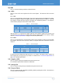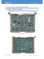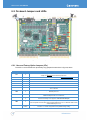
1
US SER MAN NUAL CP PU-71--15 (D DPD5) Core i7 7 VMEbus SBC S Module e First edition – June J 2013 – DP PD5MAN101 DIGITAL TEC CHNOLOGIES S FOR A BETT TER WORLD www.eurotech.co om Preface Thank you for choosing the CPU-71-15. Please read this manual before using the CPU-71-15 so that you may obtain the greatest benefit from using the device. This manual presents the specifications, functions, and method of use of the CPU-71-15. Eurotech has made every effort to carefully inspect each product and has taken great care to package and to ship the product. In the unlikely event of the product’s failure to operate normally due to problems in shipping or otherwise, the company will repair or replace the product at its own responsibility. If you have any questions, contact your local Eurotech Sales Office. Presence, page 57 for full contact details. See Eurotech Worldwide Trademarks All trademarks both marked and not marked appearing in this document are the property of their respective owners. This document does not give permission to the implementation of patents or other rights held by Eurotech or third parties. Document Revision History VERSION First edition © 2013 Dynatem Inc. DATE June 2013 Issued Publication Number DPD5MAN101 Table of Contents Table of Contents Document Revision History ......................................................................................................................... 2 Table of Contents ......................................................................................................................................... 3 1. Important User Information ...................................................................................................................... 5 1.1 Safety Notices and Warnings ................................................................................................................ 5 1.2 Life Support Policy ................................................................................................................................ 7 1.3 Warranty ................................................................................................................................................ 7 1.4 RoHS..................................................................................................................................................... 7 1.5 Technical Assistance ............................................................................................................................. 7 1.6 Conventions .......................................................................................................................................... 7 2. Summary ................................................................................................................................................... 9 2.1. Features ............................................................................................................................................... 9 2.2. Block Diagram .................................................................................................................................... 10 3. Hardware Specifications ........................................................................................................................ 11 3.1. Processor ........................................................................................................................................... 11 3.1.1. Processor Options...................................................................................................................... 11 3.1.2. Cache Memory ........................................................................................................................... 11 3.1.3. I/O Address Map ........................................................................................................................ 11 3.1.4. Memory Address Map ................................................................................................................ 12 3.1.5. CPLD Internal Register .............................................................................................................. 12 3.2. Memory .............................................................................................................................................. 13 3.2.1. Main Memory ............................................................................................................................. 13 3.2.2. Boot ROM .................................................................................................................................. 13 3.2.3. External Memory Interface ......................................................................................................... 14 3.3. Communication Specifications............................................................................................................ 14 3.3.1. Graphics .................................................................................................................................... 14 3.3.2. PCI Express ............................................................................................................................... 15 3.3.3. USB ........................................................................................................................................... 15 3.3.4. Serial ATA .................................................................................................................................. 15 3.3.5. Ethernet ..................................................................................................................................... 15 3.3.6. SMBus(System Management Bus) ........................................................................................... 15 3.3.7. PCI ............................................................................................................................................. 16 3.3.8. LPC ............................................................................................................................................ 16 3.4. I/O ...................................................................................................................................................... 17 3.4.1. GPIO .......................................................................................................................................... 17 3.4.2. Graphics LVDS .......................................................................................................................... 17 3.4.3. Analog VGA ............................................................................................................................... 17 3.4.4. Suspend Status .......................................................................................................................... 17 4. Mechanical Specifications ..................................................................................................................... 19 4.1. External Dimension ............................................................................................................................ 19 4.2. Front Panel ......................................................................................................................................... 20 4.3. Heat Sink............................................................................................................................................ 21 ............................................................................................................................ Error! Bookmark not defined. 5. PMC Support and Power Cycling .......................................................................................................... 23 5.1. Optional PMC Module Support ........................................................................................................... 23 5.1.1. General ...................................................................................................................................... 23 5.1.2. VI/O............................................................................................................................................ 23 5.1.3. JN4 I/O Expansion ..................................................................................................................... 23 DPD5MAN101 3 CPU-71-15 - User Manual 5.1.4. Mechanical Drawing ................................................................................................................... 23 5.2. Power Sequence ................................................................................................................................ 24 6. Connectors, Jumpers, and LEDs ........................................................................................................... 25 6.1. CPU-71-15 Placement Plans .............................................................................................................. 25 6.2. On-board Jumpers and LEDs ............................................................................................................. 26 6.2.1. User and Factory Option Jumpers (JPx) .................................................................................... 26 6.3. Connector Functionality and Pinouts .................................................................................................. 27 6.3.1. CN1 (SPI-ROM writing connector) ............................................................................................. 27 6.3.2. CN3 (CPLD data writing connector) ........................................................................................... 27 6.3.3. J29 LPC Off-Board Connector ................................................................................................... 27 6.3.4. J1 Front Panel Gigabit Ethernet Port.......................................................................................... 27 6.3.5. J2 Dual Front Panel SATA Port Connector ................................................................................ 28 6.3.6. J26 Front Panel VGA Connector ................................................................................................ 28 6.3.7. J27 Front Panel LVDS Connector .............................................................................................. 29 6.3.8. J28 Front Panel PS/2 Mouse & Keyboard Connector ................................................................ 29 6.3.9. USB1 – USB5 Front Panel USB Ports ....................................................................................... 29 6.3.10. P1 & P2 & P0 (VMEbus backplane connectors) ....................................................................... 30 7. System Specifications ............................................................................................................................ 33 7.1. Power Supply ..................................................................................................................................... 33 7.2. Electrical Specifications ...................................................................................................................... 33 7.2.1. GPIO .......................................................................................................................................... 33 7.3. Environmental Specifications ............................................................................................................. 33 8. BIOS Setup .............................................................................................................................................. 35 8.1. Main Menu ......................................................................................................................................... 35 8.1.1. System Date .............................................................................................................................. 35 8.1.2. System Time .............................................................................................................................. 35 8.1.3. System Information .................................................................................................................... 35 8.1.4. Boot Features ............................................................................................................................ 36 8.1.5. Error Manager ............................................................................................................................ 36 8.2. Advanced Menu ................................................................................................................................. 37 8.2.1. Select Language ........................................................................................................................ 37 8.2.2. ACPI Configuration .................................................................................................................... 37 8.2.3. Processor Configuration ............................................................................................................. 38 8.2.4. Peripheral Configuration ............................................................................................................ 41 8.2.5. HDD Configuration ..................................................................................................................... 41 8.2.6. Memory Configuration ................................................................................................................ 42 8.2.7. System Agent (SA) Configuration .............................................................................................. 43 8.2.8. South Bridge Configuration ........................................................................................................ 47 8.2.9. Network Configuration................................................................................................................ 50 8.2.10. LPC Configuration .................................................................................................................... 50 8.2.11. SMBIOS Event Log .................................................................................................................. 51 8.2.12. ME Configuration ..................................................................................................................... 51 8.2.13. Thermal Configuration .............................................................................................................. 52 8.2.14. ICC Configuration..................................................................................................................... 53 8.2.15. Intel Rapid Start Technology .................................................................................................... 54 8.3. Security Menu .................................................................................................................................... 54 8.4. Boot Menu .......................................................................................................................................... 54 8.5. Exit Menu ........................................................................................................................................... 55 Eurotech Worldwide Presence .................................................................................................................. 57 4 DPD5MAN101 Important User Information 1. Important User Information In order to lower the risk of personal injury, electric shock, fire, or equipment damage, users must observe the following precautions as well as good technical judgment, whenever this product is installed or used. All reasonable efforts have been made to ensure the accuracy of this document; however, Eurotech assumes no liability resulting from any error/omission in this document or from the use of the information contained herein. Eurotech reserves the right to revise this document and to change its contents at any time without obligation to notify any person of such revision or changes. Reproduction of all or part of this document without Eurotech’s permission is prohibited. 1.1 Safety Notices and Warnings The following general safety precautions must be observed during all phases of operation, service, and repair of this equipment. Failure to comply with these precautions or with specific warnings elsewhere in this manual violates safety standards of design, manufacture, and intended use of the equipment. Eurotech assumes no liability for the customer’s failure to comply with these requirements. The safety precautions listed below represent warnings of certain dangers of which Eurotech is aware. You, as the user of the product, should follow these warnings and all other safety precautions necessary for the safe operation of the equipment in your operating environment. Alerts that can be found throughout this manual The following alerts are used within this manual and indicate potentially dangerous situations. Danger, electrical shock hazard: Information regarding potential electrical shock hazards: Personal injury or death could occur. Also damage to the system, connected peripheral devices, or software could occur if the warnings are not carefully followed. Appropriate safety precautions should always be used, these should meet the requirements set out for the environment that the equipment will be deployed in. Warning: Information regarding potential hazards: Personal injury or death could occur. Also damage to the system, connected peripheral devices, or software could occur if the warnings are not carefully followed. Appropriate safety precautions should always be used, these should meet the requirements set out for the environment that the equipment will be deployed in. Information and/or Notes: These will highlight important features or instructions that should be observed. Protect the device from vibration and impact Do not place the product in a location where it can fall or can be subject to vibration or impact because this may cause device failure. Do not modify the device For safety reasons, under no circumstances should you modify the device. Eurotech will not repair products that have been modified. DPD5MAN101 5 CPU-71-15 - User Manual Protect the product from water and chemicals Contact between the product and water or chemicals can result in product failure, electrocution, or fire. Protect the product from foreign material Make sure that foreign material does not get into the product during use, storage, or transport because this can result in product failure. Use precautions in handling to ensure that you are not injured The sharp projections on this product may cause injury. Take care in handling this product in order to avoid injury. Do not disassemble the product In order to maintain guaranteed product performance, do not disassemble this product under any circumstances. Keep the product away from radios and TVs Do not use the product near radios, television sets, or other devices generating strong magnetic or electrical fields. This could result in failure or malfunction. Keep the product away from flame, humidity, and direct sunlight Do not use or store the product in any of the following locations, as this could result in product failure: Places where there is fire Locations high in humidity or exposed to rain Locations exposed to direct sunlight Dusty or dirty locations Locations containing excessive water or chemical vapors Install the product in well-ventilated locations Install the product in well-ventilated locations to efficiently disperse heat generated by the product. Remove the power plug from the receptacle when not using the product Turn off the main switch and remove the power plug from the receptacle when not using the product or when there is the risk of lightning strike. Use the device within rated parameters Be sure to use the product within the ratings specified in this manual. Failure to do so may result in malfunction. Use care when cleaning the product If the product becomes dirty, wipe it with a dry soft cloth. A thinned neutral cleaner may be used if the product is particularly dirty. Do not use benzene, thinners, or other solvents under any circumstances. Ground the product in order to prevent electrocution Be sure to ground the product by connecting it to a 3-pole AC receptacle or by using an AC receptacle having a grounding terminal. Dispose of the product properly Use appropriate methods for handling industrial wastes when disposing of this product. Wire the product correctly Failure to wire the product correctly can result in malfunction or fire. Read this manual and wire the product correctly. 6 DPD5MAN101 Important User Information Use antistatic precautions This product comprises electronic parts that are highly susceptible to static electricity. Static electricity can cause the product to malfunction. Take care not to touch any of the terminals, connectors, ICs, or other parts with the hands. Do not use a malfunctioning product Stop using the product if you believe it is malfunctioning. Continuing to use a malfunctioning product can cause the malfunction to spread to other products and can cause short circuits or fire. 1.2 Life Support Policy Eurotech products are not authorized for use as critical components in life support devices or systems without the express written approval of Eurotech. 1.3 Warranty For warranty terms and conditions users should contact their local Eurotech Sales Office. See Eurotech Worldwide Presence, page 57 for full contact details. 1.4 RoHS This device, including all its components, subassemblies and the consumable materials that are an integral part of the product, has been manufactured in compliance with the European directive 2002/95/EC known as the RoHS directive (Restrictions on the use of certain Hazardous Substances). This directive targets the reduction of certain hazardous substances previously used in electrical and electronic equipment (EEE). 1.5 Technical Assistance If you have any technical questions, cannot isolate a problem with your device, or have any enquiry about repair and returns policies, contact your local Eurotech Technical Support Team. For the CPU71-15, your first point of contact for technical help should be Dynatem at (949)855-3235 or [email protected] See Eurotech Worldwide Presence, page 57 for full contact details. Transportation When transporting any module or system, for any reason, it should be packed using anti-static material and placed in a sturdy box with enough packing material to adequately cushion it. Warning: Any product returned to Eurotech that is damaged due to inappropriate packaging will not be covered by the warranty. 1.6 Conventions The following table describes the conventions for signal names used in this document. Convention GND # + NC RSVD DPD5MAN101 Explanation Digital ground plane Active low signal Positive signal in differential pair Negative signal in differential pair No connection Use is reserved to Eurotech 7 CPU-71-15 - User Manual 8 DPD5MAN101 Summary 2. Summary CPU-71-15 is a VMEbus Single Board Computer (SBC) Module based on Intel® CoreTM i7 mobile processor. It is compatible with VME64 (ANSI/VITA 1-1994) and VME64x (VITA 1.1-1997) standards which are backwards compatible the original VMEbus Specification (ANSI/IEEE STD1014-1987). Based on Hyper-Threading technology, the Intel® CoreTM i7 2610UE mobile processor enables simultaneous performance of 4 threads on dual-core, and is suited for applications requiring high performance. Performance in single thread is improved by the Turbo Boost function. It also supports dual displays with its built-in High-performance graphics function. It speeds up encryption and decryption with its built-in AES code engine. Having direct-mounted DDR3-1333 supporting ECC as the main memory, the CPU-71-15 is suitable for embedded systems requiring high reliability and high performance. Maximum memory capacity is upgradable to 8GB but ships standard OTS with 4GB. The memory automatically corrects 1 bit corruption within 72 bits, and can also detect 2 bit corruption. The CPU-71-15 was introduced by Dynatem using part number DPD5. 2.1. Features CPU-71-15 has the following features: Intel® CoreTM i7 mobile processor ECC supported DDR3-1333 memory direct-mounted on board (maximum capacity of memory: 8GB) 1 port of 10/100/1000Base-T Ethernet at front panel 2 ports of 10/100BaseTX Ethernet on P2 or 2 ports of 10/100/1000BaseTX Ethernet on P0 1 port of LVDS graphics interface at front panel 1 port of Analog SVGA graphics at front panel 5 ports of USB2.0 interface at front panel 1 PS/2 Connector for Mouse/Keyboard Interface at front panel 2 ports of SATA at 6.0 Gb/s interface at front panel 3 RS-232 COM ports routed to P2 backplane connector, 2 from the Super I/O chip and one from a Silicon Labs CP2102 USB-UART adapter 1 port of SATA at 3.0 Gb/s interface at optional CFast connector 1 port of SATA at 3.0 Gb/s interface at optional P0 VMEbus backplane connector 1 optional PMC site with 32 bit @ 33 MHz PCI (with XMC connector for a x8 PCI Express interface) 2nd optional PMC site with 32 bit @ 33 MHz PCI 2 ports of PCI Express X1 link Universe IID for a VMEbus interface Various OS including Windows 7, VxWorks, and Linux are supported RoHS compliant DPD5MAN101 9 CPU-71-15 - User Manual 2.2. Block Diagram CPU-71-15 Block Diagram is shown in Fig.1. Fig.1 Block Diagram 10 DPD5MAN101 Hardware Specifications 3. Hardware Specifications 3.1. Processor 3.1.1. Processor Options Intel’s ®CoreTM i7-2610UE Mobile Dual Core CPU at 1.5GHz (TDP:17W) is the off-the-shelf processor, preferable for embedded applications with broader temperature requirements. Intel® Core i7-2655LE Mobile Dual Core CPU at 2.2GHz (TDP:25W) is optional. 3.1.2. Cache Memory CPU-71-15 has the following cache memory: L1 cache 32kB for data, 32kB for instruction (per core) L2 cache 256kB for data and instruction (per core) L3 cache (shared by all cores) o CoreTM i7-2610UE:4MB 3.1.3. I/O Address Map I/O space Address Map is shown in Table 1. Table 1. Device DMA Controller Interrupt Controller LPC SIO Interrupt Controller Timer/Counter LPC SIO Timer/Counter Microcontroller NMI Controller Microcontroller RTC Controller DMA Controller Reset Generator DMA Controller Interrupt Controller Power Management Interrupt Controller DMA Controller PCI and Master Abort Serial ATA Serial ATA Serial ATA Serial ATA Interrupt Controller Reset Generator DPD5MAN101 I/O space Address Map Address 0000h - 001Fh 0020h - 002Dh 002Eh - 002Fh 0030h - 003Dh 0040h - 0043h 004Eh - 004Fh 0050h - 0053h 0060h 0061h 0062h - 0066h 0070h - 0077h 0080h - 0091h 0092h 0093h - 009Fh 00A0h - 00B1h 00B2h - 00B3h 00B4h - 00BDh 00C0h - 00DFh 00F0h 0170h - 0177h 01F0h - 01F7h 0376h 03F6h 04D0h - 04D1h 0CF9h 11 CPU-71-15 - User Manual 3.1.4. Memory Address Map Memory space Address Map is shown in Table 2. Table 2. Memory space Address Map Address 0000_0000h 8000_0000h Device Lowest 2 GB of Main Memory PLX PEX8112 PCI Express - PCI Bridge to the Universe IID VMEbus adapter & the PMC Sites PCI Express Device Chipset, BIOS, etc Higher 2 GB of DRAM on Cards w/ 4 GB DRAM or Higher 6 GB of DRAM on Cards w/ 8 GB DRAM A000_0000h E000_0000h 1_0000_0000h 1_0000_0000h --- 7FFF_FFFFh --- 9FFF_FFFFh ------or --- BFFF_FFFFh FFFF_FFFFh 1_7FFF_FFFFh 2_7FFF_FFFFh . 3.1.5. CPLD Internal Register CPLD Internal Register is shown in Table 3. Table 3. CPLD Internal Register map Address 0000h 0001h 0002h 0003h Register Name LED Control Register Status Register Thermal Monitor Select Register Thermal Monitor Register Item 3.1.5.1. 3.1.5.2. 3.1.5.3. 3.1.5.4. A CPLD is mounted as internal control logic and for power sequencing. The CPLD’s internal register is accessible by the LPC bus of 3.3.8 LPC on page 16. Its base address is 0280h. The register is configured for 8 bits. Both Read (shown below as: R) and Write (shown below as: W) operations are performed as 8-bit transfers. R/W : Read and Write RO : Read only WO : Write only 3.1.5.1. LED Control Register (offset:0000h) This register controls LED on CPU-71-15. Table 4. bit 7..3 2 Name RSVD LED_EN 1 RED_LED 0 GRN_LED LED Control Register Meaning Initial Value 00000 0 Access RO R/W 1:LED (RED) On 0:LED (RED) Off 0 R/W 1:LED (GRN) On 0:LED (GRN) Off 0 R/W RSVD 1:RED/GRN_LED control enabled 0:RED/GRN_LED control disabled ※ LED_EN=’0’ : RED_LED turns on during assertion of the Platform reset that is output by PCH,while GRN_LED turns on during de-assertion. Please refer to 3.5. LED on page 18 for further details. 12 DPD5MAN101 Hardware Specifications 3.1.5.2. Status Register (offset:0001h) This register shows the logic of SPD Write Protect signal and input signal from carrier board. Table 5. bit 7..4 3 2 1 0 Status Register Name Meaning RSVD RSVD BIOS_DISABLE# Request signal from carrier board THRM# 1:Temperature sensor on carrier board shows a normal value 0:Temperature sensor on carrier board is shows an abnormal value BATLOW# 1:battery voltage on carrier board is a normal value SPD_WP Initial Value 000000 - Access RO RO RO - RO 1 R/W 0:battery voltage on carrier board is an abnormal value WP of EEPROM for SPD Write 0 when rewriting software 3.1.5.3. Thermal Monitor Select Register (offset:0002h) This register selects a thermal monitor connected to the CPLD that is being read out. Table 6. bit 7..2 1..0 Name RSVD THRM_MONI_SEL Thermal status register Meaning RSVD Thermal monitor temperature selected from the following options can be read out by thermal monitor register (offset:0003h). 11:RSVD 10:GBE_THRM (ambient temperature of GbE(82579)) 01:DDR3B_THRM (ambient temperature of DDR3(solder side)) 00:DDR3A_THRM (ambient temperature of DDR3 (component side)) Initial Value 000000 00 Access RO R/W 3.1.5.4. Thermal Monitor Register (offset:0003h) This register displays temperature value read out by the thermal monitor. Table 7. bit 7..0 Name THRM Thermal Monitor Register Meaning Displays the temperature value read out from the thermal monitor selected by THRM_MONI_SEL (0 to 255℃, 1℃/LSB) Initial Value 00000000 Access RO 3.2. Memory CPU-71-15 memory is shown below. 3.2.1. Main Memory The main memory of CPU-71-15 is DDR3-1333 SDRAM. 4 GB capacity comes standard off-the-shelf but optional versions with 1GB, 2GB, or 8GB can be specially ordered. It supports ECC, automatically corrects 1-bit error, and also detects 2-bit errors. 3.2.2. Boot ROM This is a SPI-FLASH memory directly-mounted on CPU-71-15 with 8MB of capacity. It stores UEFI (functionally, the “BIOS”) code and configuration data. DPD5MAN101 13 CPU-71-15 - User Manual 3.2.3. External Memory Interface CPU-71-15 has the following 2 external memory interfaces for mass storage devices and boot options: Serial ATA. CPU-71-15 has two 6 Gb/s SATA ports (SATA0 and SATA1) accessible at the front panel, which can boot from mass storage devices through cable connections. SATA2 is a 3 Gb/s port and it is routed to the optional P0 connector to the backplane. SATA3 is also a 3 Gb/s port and it is routed to a CFast connector on-board that facilitates self-contained OS booting. USB. CPU-71-15 has 5 USB ports accessible at the front panel, which can boot from USB floppy or USB-CD (DVD)-ROM or a USB flash drive. 3.3. Communication Specifications CPU-71-15 has the following communication specifications with external devices. 3.3.1. Graphics The CPU-71-15 has two graphics ports from the QM67 PCH that are accessible from the front panel. An SVGA Port with a 340.4 MHz RAMDAC that supports resolutions up to 2048 x 1536 pixels @ 75 Hz. Three 8-bit DACs provide R, G, and B. An LVDS port with three differential data bits routed to front panel connector J27 for flat panel interfacing is compatible with the ANSI/TIA/EIA-644 specification. The i7 processor provides 16 PCI Express lanes that may be used for graphics expansion. Eight of these PCI Express lanes remain unrouted but the other 8 have been brought to optional XMC connector, J15. XMC cards cannot be populated on off-the-shelf CPU-71-15 cards as they will mechanically conflict with the front panel connectors. Table 8. 14 VMEbus Pin Name PCI Express Lane PCIE15 15 PCIE14 14 PCIE13 13 PCIE12 12 PCIE11 11 PCIE10 10 PCIE9 9 PCIE8 8 PCIE7 7 PCIE6 6 PCIE5 5 PCIE4 4 PCIE3 3 PCIE2 2 PCIE1 1 PCIE0 0 PCI Express Graphics Link Configuration Link Configuration 1 Link Configuration 2 Link Configuration 3 X4 X8 (unrouted) X4 X 16 X8 X8 (routed to the optional XMC connector J15) DPD5MAN101 Hardware Specifications 3.3.2. PCI Express CPU-71-15 is compliant with PCI Express Rev2.0 standard. The CPU has 16 lanes of PCI Express that were discussed in the previous section. The QM67 PCH offers 8 lanes of PCI Express. Table 9 shows how the 8 PCI Express lanes from the PCH are used and what devices they interface to. Table 9. PCH PCI Express Configuration PCH PCI Express lane Application PCIE1 PLX PEX8112 PCI Express to PCI Bridge PCIE2 82579-LM 1 Gbps Front Panel 1 Ethernet Port PCIE3 Not Used PCIE4 Not Used PCIE5 PCIE6 PCIE7 82571EB Dual Ethernet Controller where the ports are routed to the backplane PCIE8 3.3.3. USB CPU-71-15 has 5 USB ports accessible from the front panel that are fully compliant with the USB2.0 standard. 3.3.4. Serial ATA CPU-71-15 has 4 ports of Serial ATA in total; 2 ports (SATA0/1) of Serial ATA 3 (maximum transfer speed: 6Gb/s) routed to a dual stacked connector on the front panel and 2 ports (SATA2/3) of Serial ATA 2 (maximum transfer speed: 3Gb/s) routed to an optional P0 backplane connector and a CFast connector, respectively. 3.3.5. Ethernet CPU-71-15 has an Ethernet port compliant with the 10/100/1000Base-T standard. An 82571EB provides: two 10/100Base-T ports (routed to the P2 backplane connector) or two 10/100/1000Base-T ports (routed to the optional P0 backplane connector (set at the factory at customer’s request)). 3.3.6. SMBus(System Management Bus) CPU-71-15 has an I2C multiplexer at the SMBus interface to carrier board. It also has a SMBus port compliant with the SMBus 2.0 standard. The SMBus address map is shown in Table 10. Table 10. SMBus Address Map Address 1010 000b 1010 001b 1110 000b Device Main Memory SPD (channel A) Main memory SPD (channel B) 2 I C multiplexer (PCA9544APW) I2C multiplexer channel map is shown in Table 11. Table 11. Device Unused Unused Super I/O Unused 2 I C multiplexer channel map Address 0 1 2 3 Channel is not selected after BIOS start up. Do not switch to channel 0 or channel 3 as they are 2 unused. Please refer to the PCA9544APW (NXP) datasheet for I C multiplexer setting method. DPD5MAN101 15 CPU-71-15 - User Manual 3.3.7. PCI CPU-71-15 has a 32bit/33MHz PCI bus compliant with the PCI Local Bus Specification Revision 2.3 standard. The PCI bus interface is provided by a PLX PEX8112 bridge that adapts from one (x1) PCI Express lane off the QM67 and then is used to interface to the Idt Universe IID PCI bus to VMEbus controller. Additionally it interfaces to the two optional PMC sites. The signal voltage on the PCI bus is 3.3VDC only. PCI devices are shown in Table 12. Table 12. Bus number Device model number Device number Function number Device 0 0 DRAM Controller Intel Core ® TM i7/i5 0 PCI Express Controller 1 ® Intel Core TM i7/i5 1 PCI Express Controller 2 Intel Core ® TM i7/i5 2 PCI Express Controller 3 Intel Core ® TM i7/i5 2 0 Integrated Graphics Device Intel Core ® TM i7/i5 6 0 PCI Express Controller 4 Intel Core ® TM i7/i5 0 Intel Management Engine Interface #1 1 1 ® ® Intel QM67 Intel Management Engine Interface #2 ® Intel QM67 2 IDE-R Intel QM67 3 KT Intel QM67 25 0 Gigabit Ethernet Controller Intel QM67 26 0 to 7 USB EHCI Controller #2 Intel QM67 0 to 7 Intel High Definition Audio Controller Intel QM67 0 PCI Express Port 1 Intel QM67 1 PCI Express Port 2 Intel QM67 2 PCI Express Port 3 Intel QM67 3 PCI Express Port 4 Intel QM67 4 PCI Express Port 5 Intel QM67 5 PCI Express Port 6 Intel QM67 6 PCI Express Port 7 Intel QM67 7 PCI Express Port 8 Intel QM67 29 0 to 7 USB EHCI Controller #1 Intel QM67 30 0 PCI-to-PCI Bridge Intel QM67 0 LPC Controller Intel QM67 2 SATA Controller #1 Intel QM67 3 SMBus Controller Intel QM67 5 SATA Controller #2 Intel QM67 6 Thermal Subsystem Intel QM67 - PCI Express - 22 27 0 28 31 M(*4) List of PCI devices - ® ® ® ® ® ® ® ® ® ® ® ® ® ® ® ® ® ® ® ® ® ® *4:M depends on the largest bus number shown on PCI Express. 3.3.8. LPC CPU-71-15 has a port compliant with the LPC1.1 standard. The LPC bus is used for communication with the LPC47M107S-MS Super I/O chip. This device is used by the BIOS and provides two COM ports and an LPT1 port that are accessible from the P2 backplane connector, and a PS/2 port for mouse and keyboard interfacing that is available from a front panel connector, J28. 16 DPD5MAN101 Hardware Specifications 3.4. I/O CPU-71-15 has the following interfaces to external devices. 3.4.1. GPIO CPU-71-15 has a GPI control register and a GPO control register. The features of GPIO are shown below. 3.4.1.1. GPI CPU-71-15 is equipped with 4 general inputs. They can be read out from the Intel QM67 PCH register. GPI is set as input pin in BIOS. The register where GPI is allocated is shown in Table 13. If the GPI line’s jumper is closed, that GPI line will be connected to its corresponding GPO line. For example, if JP5 is shunted (closed), the GPO2 will be routed to GPI2. Table 13. GPI control register Signal Intel QM67connecting pin Supporting register Bit Jumper GPI0 GPIO68 GP_LVL3 bit 4 JP3 GPI1 GPIO69 GP_LVL3 bit 5 JP4 GPI2 GPIO70 GP_LVL3 bit 6 JP5 GPI3 GPIO71 GP_LVL3 bit 7 JP6 High logic level (“1”) is read from the register while High level voltage is applied to the input pin, and Low logic level (“0”) is read from the register while Low level voltage is applied to the input pin. Please refer to 7.2. Electrical Specifications on page 28 for electrical specifications. 3.4.1.2. GPO CPU-71-15 is equipped with 4 general outputs. Status can be changed by writing in the Intel QM67 PCH register. GPO is set as the output pin in BIOS. The register where GPO is allocated is shown in Table 14. Table 14. Signal Intel QM67connecting pin GPO control register Supporting register Bit Initial setting (logic level) GPO0 GPIO8 GP_LVL bit 8 High GPO1 GPIO15 GP_LVL bit 15 Low GPO2 GPIO24 GP_LVL bit 24 Low GPO3 GPIO28 GP_LVL bit 28 Low It outputs High level voltage when High logic level (“1”) is written in the register, while it outputs Low level voltage when Low logic level (“0”) is written in it. Please refer to 7.2. Electrical Specifications on page 28 for electrical specifications. 3.4.2. Graphics LVDS CPU-71-15 has an LVDS port, available at front panel connector J27. It is confirmed to operate at the resolution of 1920×1200. 3.4.3. Analog VGA CPU-71-15 has an Analog VGA port, available at front panel connector J26. 3.4.4. Suspend Status CPU-71-15 routes the SUS_STAT#/SUS_S3#/SUS_S4#/SUS_S5# signals to LEDs. See Section 6.2 for LED locations and descriptions. DPD5MAN101 17 CPU-71-15 - User Manual 18 DPD5MAN101 Mechanical Specifications 4. Mechanical Specifications CPU-71-15 is compliant with the VMEbus & VME64 Specification. Mechanical specifications are shown in Table 16. Table 15. Characteristic Mechanical Specifications Contents PC Board Form Factor 233.35mm high x 153.67mm wide x 2.31mm thick Backplane Connectors 96 pin DIN 603-2-IEC-CO96Mx-xxx connectors in compliance with the VME64 Draft Specification Weight 680g (Including heat sink and front panel) 4.1. External Dimension External dimensions of CPU-71-15 are shown in Fig.2. Unit : mm (inches) *5: Height of the mounted components (on the solder side) does not exceed 70 mils.. Fig.2 External dimensions of CPU-71-15 DPD5MAN101 19 CPU-71-15 - User Manual 4.2. Fro ont Pan nel The D DPD5’s front panel usess a non-stan ndard length h and a spe ecial captive screw (deta ail G, part # 11408 84RS.375CS SS12). The iridite i finish is Mil-C-5541 1. Fig.3. Front panel mechanical m and slkscreen draw wings 20 DP PD5MAN101 Mechanical Specifications 4.3. Heat Sink The CPU-71-15 comes with a heat sink. The heat sink mainly comes in contact with the CPU, the PCH chipset, and the 82571EB dual Ethernet Controller that routes to the backplane. These are the onboard chips with exposed dies. The fins aid in airflow cooled VMEbus chasses as fans must force air from top to bottom or vice versa. The fins will channel the air and add to the surface area that is exposed to forced air. The measurements in the drawing are in mm. Table 16. Processor Type ® TM Intel Core i7-2610UE DPD5MAN101 Required heat resistance for cooling system Heat resistance of cooling system Below 2.35℃/W 21 CPU-71-15 - User Manual 22 DPD5MAN101 Cautiions for Des signing a Ca arrier Board d 5. PM MC Sup pport and a Po ower Cyclin C ng 5.1. Op ptional PMC P Mo odule Support 5.1.1. Gen neral Versions of th V he CPU-71-15 that suppo ort one or two o PMC sites must be spe ecial ordered d because they confflict mechaniically with the e front panell connectors.. The first sitte, which alsso supports a x8 XMC C interface, will w conflict with w the dual stacked SAT TA connector, 4 of the 5 front f panel USB portts, and the frront panel Etthernet port. The second d PMC site co onflicts with one of the USB portts, the PS/2 mouse and keyboard k port, and the LV VDS port. T PLX PEX The X8112 chip bridges one PCI P Express Rev 2 lane (@ ( 2.5 Gbps) to the 32 bit @ 33 MHz. Th he PCI bus iss shared betw ween the Un niverse and th he two option nal PMC site es. The Universe e limits the PC CI bus’s freq quency to 33 MHz. 5.1.2. VI/O O T PEX8112 The 2 supports a signalling bu us of 5.0 VDC C. 5.1.3. JN4 4 I/O Expa ansion T The first PMC C site’s I/O may m be routed d through the J14 (JN4 PMC P functionality) to the e optional P0 0 backplane co onnector. Th he second site’s s I/O ma ay be routed d through J2 24 to the P2 2 backplane e onnector. co 5.1.4. Mec chanical Drawing D The drawing below T b showss how a PMC C card will sitt on the CPU U-71-15. Spa ace between the PMC ca ard and the CPU-71-15’s C s printed circ cuit board (PC CB) is 0.370””. DPD5MAN1 101 23 CPU-71-15 - User Manual 5.2. Power Sequence 12V and 5VDC on the VMEbus have no power sequence but 12 VDC is required to switch on the onboard 5 VDC which is the source for all other voltages. For internal use: Turn the board power off when connecting the SF100 programming tool to the CN1 connector for BIOS reprogramming. Do not send the following signals when the CB_RESET# signal is being asserted. Signals LPC_SERIRQ VGA_I C_DAT 2 KBD_A20GATE 2 SDVO_I C_DAT GPI 0 to 3 LPC_DRQ 0 to 1# 2 KBD_RST# LPC_AD 0 to 3 LVDS_I C_DAT Please make sure that the following signals will have no problem in your design even if voltage is applied from the CPU-71-15 while the carrier board power is OFF. Signals LPC_SERIRQ 2 SUS_S4# 2 PCI_FRAME# LVDS_I C_CK 2 LVDS_I C_DAT SUS_S5# PCI_STOP# LVDS_I C_DAT VGA_I C_DAT 2 I C_CK PCI_IRDY# VGA_HSYNC GPI 0 to 3 I C_DAT 2 PCI_TRDY# VGA_VSYNC KBD_RST# ATA_ACT# PCI_SERR# VGA_I C_CK 2 2 2 VGA_I C_DAT KBD_A20GATE GPO 0 to 3 PCI_PERR# LPC_DRQ 0 to 1# THRMTRIP# PCI_DEVSEL# PCI_CLK CB_RESET# PCI_GNT0 to 3# PCI_LOCK# LPC_CLK PCI_RESET# PCI_AD0 to 31 LVDS_BKLT_EN LPC_FRAME# SUS_STAT# PCI_C/BE0 to 3# LVDS_VDD_EN LPC_AD0 to 3 SUS_S3# PCI_PAR LVDS_BKLT_CTRL - If your design does not conform to the above description, please check before using to avoid any problems. 24 DPD5MAN101 Connectors and Jumpers 6. Connectors, Jumpers, and LEDs 6.1. CPU-71-15 Placement Plans A photograph of the CPU-71-15, component side, is shown in Fig.4 with connectors and major components labelled. The solder side is shown in Fig. 5. Fig. 6 labels user option jumpers and LEDs. PB1 J26 J27 LVDS VGA J28 J1 USB5,4 J2 USB3,2,1 USB PS/2 CPU SATA Battery DRAM SI/O J29 CFast CPU PCH Universe P0 P2 P1 Fig.4 Component side DRAM J6 and J7 CN3 PEX8112 CPLD CN1 Fig.5 Solder side DPD5MAN101 25 CPU-71-15 - User Manual 6.2. On-board Jumpers and LEDs JP22 JP1 JP21 JP3 D25 D33 D32 LED1 D36 D34 D24 JP18 JP17 JP19 LED2 JP2 D35 JP6 JP4 JP5 Fig.6 Locations of User Option Jumpers & LEDs 6.2.1. User and Factory Option Jumpers (JPx) The CPU-71-15 has several user (and factory only) jumpers that are shown in figure 6, above. Jumper 26 # of Pins Description JP1 2 Clears CMOS and BIOS settings go to default when shunted for 4 seconds while power is off. Jumper JP1 must not be shunted when power is on. JP2 2 JP2 will route BATLOW# to Ground when shunted. JP2 must be left open. JP3 2 JP3 routes GPI0 to GPO0 when shunted. JP4 2 JP4 routes GPI1 to GPO1 when shunted. JP5 2 JP5 routes GPI2 to GPO2 when shunted. JP6 2 JP6 routes GPI3 to GPO3 when shunted. JP17 2 The CPU-71-15 will be hardware initialized to operate as a VMEbus slot 1 bust controller when JP17 is shunted. JP18 2 The CPU-71-15 will be reset by VMEbus resets when JP18 is shunted and JP22 is shunted between pins 2 & 3. JP19 2 The VMEbus SYSRESET generated by the Universe IID on the CPU-71-15 will be routed to the VMEbus backplane when JP19 is shunted. JP21 2 The CPU-71-15 will attempt to boot from an LPC BIOS via connector J29 when JP21 is shunted and this functionality is not supported. JP21 must be left open. JP22 3 The VMEbus SYSRESET as generated or received by the Universe IID will reset the CPU-71-15’s CPU and system resources when JP22 is shunted between pins 2 & 3. Otherwise JP22 must be shunted between pins 1 & 2. J6 & J7 18 each Unpopulated jumper networks for SATA redriver configuring for dual SATA port front panel connector J2. Default configurations were qualified through testing. DPD5MAN101 Connectors and Jumpers 6.2.2. On-board LEDs The CPU-71-15 has LEDs that provide info on system status and are shown in figure 6, above. LED Color LED1 Green When LED1 is lit, the on-board power supplies are on and the board should be running. Description LED2 Red When LED2 is lit, the on-board power supplies are in standby mode and the board will not run. D24 Red? D24 is turned on by pin PC8 (LED1) from the CFast drive at connector J25. D25 Red? D25 is turned on by pin PC9 (LED2) from the CFast drive at connector J25. D32 Green SATA Activity LED from the CPU-71-15 PCH. D33 Red Lit when THERMTRIP has been set off, indicating an overheat status. D34 Red Lit when the CPU & PCH are in Sleep State S4. D35 Red Lit when the CPU & PCH are in Sleep State S5. D36 Red Lit when SUS_STAT# has been asserted and the CPU & PCH are entering a sleep state. 6.3. Connector Functionality and Pinouts 6.3.1. CN1 (SPI-ROM writing connector) CN1 is a connector for writing BIOS data to the on-board SPI-ROM. CN3 will be removed before shipment.. 6.3.2. CN3 (CPLD data writing connector) CN3 is a connector for writing data to the on-board CPLD. CN3 will be removed before shipment. 6.3.3. J29 LPC Off-Board Connector Connector J29 provides off-board LPC routing for alternative BIOS, Super I/O, and also POST code support. This connector is intended for factory use. Here is the pinout for J29: Odd Row 1 Signal NC Even Row Signal 2 3.3 VDC 33 MHz Clock. 3 NC 4 5 AD0 6 AD3 7 AD1 8 FRAME# GND 9 AD2 10 11 RESET 12 N/C 13 N/C 14 5 VDC 15 Pullup to 3.3 VDC 16 GND 6.3.4. J1 Front Panel Gigabit Ethernet Port Connector J1 provides a 1 Gigabit/second Ethernet port accessible at the front panel. There are four differential pairs and they are bidirectional (“BI…”). Here is the pinout for J1: Pin 1 DPD5MAN101 Signal BI_DA+ 2 BI_DA- 3 BI_DB+ 4 BI_DC+ 5 BI_DC- 6 BI_DB- 7 BI_DD+ 8 BI_DD- 27 CPU-71-15 - User Manual 6.3.5. J2 Dual Front Panel SATA Port Connector Connector J2 provides two SATA ports accessible at the front panel. Both of the two SATA ports in the stacked J2 connector have this same pinout (the TxD pair is driven to J2; the RxD pair is driven from J2): Pin Signal 1 GND 2 TxD+ 3 TxD- 4 GND 5 RxD- 6 RxD+ 7 GND 6.3.6. J26 Front Panel VGA Connector J26 is a high-density DB15 VGA connector accessible from the front panel. Here is the pinout for J26: Pin 28 Signal 1 Red Output 2 Green Output 3 Blue Output 4 NC 5 HSYNC/VSYNC Return (GND) 6 Red Return (GND) 7 Green Return (GND) 8 Blue Return (GND) 9 +5 VDC 10 HSYNC/VSYNC Return (GND) 11 NC 12 DDCDAT 13 Horizontal Sync (HSYNC) Output 14 Vertical Sync (VSYNC) Output 15 DDCCLK DPD5MAN101 Connectors and Jumpers 6.3.7. J27 Front Panel LVDS Connector J27 is a Single-in-line Molex connector accessible from the front panel that provides a 3 bit differential LVDS flat panel interface. Here is the pinout for J27: Pin Signal 1 GND 2 LVDS_A_CLK+ 3 LVDS_A_CLK- 4 GND 5 LVDS_A2+ 6 LVDS_A2- 7 GND 8 LVDS_A1+ 9 LVDS_A1- 10 GND 11 LVDS_A0+ 12 LVDS_A0- 6.3.8. J28 Front Panel PS/2 Mouse & Keyboard Connector J28 is a PS/2 connector accessible from the front panel that provides interfaces for both a mouse and a keyboard. Here is the pinout for J28: Signal Pin 1 Keyboard Data 2 Mouse Data 3 GND 4 +5 VDC (via 1 amp self-resetting fuse F1) 5 Keyboard Clock 6 Mouse Clock 6.3.9. USB1 – USB5 Front Panel USB Ports Connectors USB1 – USB5 provide five USB 2.0 ports that are accessible at the front panel. Here is the pinout for any one of the five connectors.: Pin DPD5MAN101 Signal 1 +5 VDC (via 1.1 amp self-resetting fuse F2) 2 Negative Data 3 Positive Data 4 Signal GND 5 Chassis GND 6 Chassis GND 7 Chassis GND 8 Chassis GND 29 CPU-71-15 - User Manual 6.3.10. P1 & P2 & P0 (VMEbus backplane connectors) P1, P2 are the VMEbus connectors populated on standard off-the-shelf CPU-71-15 cards. They are Harting 160-pin 5-row DIN connectors. Table 17 has the pinout for the P1 connector. P1 is VMEbus spec compliant in its pinout while P2 has custom I/O routing of COM ports, SATA, LAN and LPT1. P1 uses a 5-row connector but the two outside rows (D & Z) are all no connects. The P2 pinout is in Table 18. Outside rows D&Z route the JN4 I/O from optional PMC Site 1 to the backplane as shown. The optional P0 connector (not populated on the off-the-shelf CPU-71-15) is shown in Table 19. Each pin on row F is connected to Ground. Table 17. Pin number A1 A2 A3 A4 A5 A6 A7 A8 A9 A10 A11 A12 A13 A14 A15 A16 A17 A18 A19 A20 A21 A22 A23 A24 A25 A26 A27 A28 A29 A30 A31 A32 30 RowA Signal D00 D01 D02 D03 D04 D05 D06 D07 GND SYSCLK GND DS1# DS0# WRITE# GND DTACK# GND AS# GND IACK# IACKIN# IACKOUT# AM4 A07 A06 A05 A04 A03 A02 A01 -12 VDC +5 VDC Pin number B1 B2 B3 B4 B5 B6 B7 B8 B9 B10 B11 B12 B13 B14 B15 B16 B17 B18 B19 B20 B21 B22 B23 B24 B25 B26 B27 B28 B29 B30 B31 B32 P1 VMEbus connector RowB Signal BBSY# BCLR# ACFAIL# BG0IN# BG0OUT# BG1IN# BG1OUT# BG2IN# BG2OUT# BG3IN# BG3OUT# BR0# BR1# BR2# BR3# AM0 AM1 AM2 AM3 GND NC NC GND IRQ7# IRQ6# IRQ5# IRQ4# IRQ3# IRQ2# IRQ1# +5 VDC Standby +5 VDC Pin number C1 C2 C3 C4 C5 C6 C7 C8 C9 C10 C11 C12 C13 C14 C15 C16 C17 C18 C19 C20 C21 C22 C23 C24 C25 C26 C27 C28 C29 C30 C31 C32 RowC Signal D08 D09 D10 D11 D12 D13 D14 D15 GND SYSFAIL# BERR# SYSRESET# LWORD# AM5 A23 A22 A21 A20 A19 A18 A17 A16 A15 A14 A13 A12 A11 A10 A09 A08 +12 VDC +5 VDC DPD5MAN101 Connectors and Jumpers Table 18. Pin A1 A2 A3 A4 A5 A6 A7 A8 A9 A10 A11 A12 A13 A14 A15 A16 A17 A18 A19 A20 A21 A22 A23 A24 A25 A26 A27 A28 A29 A30 A31 A32 Row A Signal COM2 TxD# COM2 RxD# COM2 RTS COM2 CTS COM3 TxD# COM3 RxD# COM3 RTS COM3 CTS ALT_BAT NC LAN3TDP LAN3RDP LAN3TDN LAN3RDN GND LAN2TDP LAN2TDN NC NC GND NC NC NC NC NC NC NC NC NC NC NC NC Pin B1 B2 B3 B4 B5 B6 B7 B8 B9 B10 B11 B12 B13 B14 B15 B16 B17 B18 B19 B20 B21 B22 B23 B24 B25 B26 B27 B28 B29 B30 B31 B32 Row B Signal +5 VDC GND N/C A24 A25 A26 A27 A28 A29 A30 A31 GND +5 VDC D16 D17 D18 D19 D20 D21 D22 D23 GND D24 D25 D26 D27 D28 D29 D30 D31 GND +5 VDC Pin C1 C2 C3 C4 C5 C6 C7 C8 C9 C10 C11 C12 C13 C14 C15 C16 C17 C18 C19 C20 C21 C22 C23 C24 C25 C26 C27 C28 C29 C30 C31 C32 Table 19. Pin A01 A02 A03 A04 A05 A06 A07 A08 A09 A10 A11 A12 A13 A14 A15 A16 A17 A18 A19 Row A Signal NC Opt LPa_DA+ Opt LPa_DB+ Opt LPb_DA+ Opt LPb_DB+ NC PIO5 PIO10 PIO15 PIO20 PIO25 PIO30 PIO35 PIO40 PIO45 PIO50 PIO55 PIO60 N/C DPD5MAN101 Pin B01 B02 B03 B04 B05 B06 B07 B08 B09 B10 B11 B12 B13 B14 B15 B16 B17 B18 B19 Row B Signal NC Opt LPa_DAOpt LPa_DBOpt LPb_DAOpt LPb_DBNC PIO4 PIO9 PIO14 PIO19 PIO24 PIO29 PIO34 PIO39 PIO44 PIO49 PIO54 PIO59 PIO64 Pin C01 C02 C03 C04 C05 C06 C07 C08 C09 C10 C11 C12 C13 C14 C15 C16 C17 C18 C19 P2 VMEbus connector Row C Signal COM1 TxD# COM1 RxD# COM1 RTS COM1 CTS COM1 DTR COM1 DSR COM1 DCD COM1 RI JN4-28 Speaker Output +5 VDC LAN2RDP LAN2RDN NC JN4-30 LPT1 STROBE# LPT1 AUTOFD# LPT1 PD0 LPT1 ERR# LPT1 PD1 LPT1 INIT# LPT1 PD2 LPT1 SLCTIN# LPT1 PD3 LPT1 PD4 LPT1 PD5 LPT1 PD6 LPT1 PD7 LPT1 ACK# LPT1 BUSY LPT1 PE LPT1 SLCT Pin D01 D02 D03 D04 D05 D06 D07 D08 D09 D10 D11 D12 D13 D14 D15 D16 D17 D18 D19 D20 D21 D22 D23 D24 D25 D26 D27 D28 D29 D30 D31 D32 Row D Signal P24-1 P24-3 P24-4 P24-6 P24-7 P24-9 P24-10 P24-12 P24-13 P24-15 P24-16 P24-18 P24-19 P24-21 P24-22 P24-24 P24-25 P24-27 P24-28 P24-30 P24-31 P24-33 P24-34 P24-36 P24-37 P24-39 P24-40 P24-42 P24-43 P24-45 GND +5 VDC Pin Z01 Z02 Z03 Z04 Z05 Z06 Z07 Z08 Z09 Z10 Z11 Z12 Z13 Z14 Z15 Z16 Z17 Z18 Z19 Z20 Z21 Z22 Z23 Z24 Z25 Z26 Z27 Z28 Z29 Z30 Z31 Z32 Row Z Signal P24-2 GND P24-5 GND P24-8 GND P24-11 GND P24-14 GND P24-17 GND P24-20 GND P24-23 GND P24-26 GND P24-29 GND P24-32 GND P24-35 GND P24-38 GND P24-41 GND P24-44 GND P24-46 GND P0 VMEbus connector Row C Signal NC GND GND GND GND NC PIO3 PIO8 PIO13 PIO18 PIO23 PIO28 PIO33 PIO38 PIO43 PIO48 PIO53 PIO58 PIO63 Pin D01 D02 D03 D04 D05 D06 D07 D08 D09 D10 D11 D12 D13 D14 D15 D16 D17 D18 D19 Row D Signal SATA2_TxLPa_DC+ LPa_DD+ LPb_DC+ LPb_DD+ SATA2_RxPIO2 PIO7 PIO12 PIO17 PIO22 PIO27 PIO32 PIO37 PIO42 PIO47 PIO52 PIO57 PIO62 Pin E01 E02 E03 E04 E05 E06 E07 E08 E09 E10 E11 E12 E13 E14 E15 E16 E17 E18 E19 Row E Signal SATA2_TX+ LPa_DCLPa_DDLPb_DCLPb_DDSATA2_Rx+ PIO1 PIO6 PIO11 PIO16 PIO21 PIO26 PIO31 PIO36 PIO41 PIO46 PIO51 PIO56 PIO61 31 CPU-71-15 - User Manual 32 DPD5MAN101 System Specifications 7. System Specifications 7.1. Power Supply Power to the CPU-71-15 is supplied through P1 & P2 (VMEbus backplane connectors), pinout on pages 30 & 31. Power supply specifications are shown in Table 20. Table 20. Item Power supply Current consumption Power supply specifications Unit Symbol Min Typ. Max VCC_12V 11.4 12 12.6 V VCC_5V 4.75 5 5.25 V VCC_RTC 2.0 3 3.3 V IVCC_12VDC - - - A IVCC_5VDC - 4.1 6.2 A IVCC_RTC - 1.4 - μA Max Unit 3.38 V 0.45 V *8: TDP:under benchmark test with a 45W processor 7.2. Electrical Specifications 7.2.1. GPIO Electrical specifications of GPIO are shown in Table 21. Table 21. GPIO electrical specifications Parameter Symbol Min Typ. GPO VOH High level output voltage IOH=-4mA VOL Low level output voltage IOL=4mA VIH High level input voltage 2.0 3.8 V VIL Low level input voltage -0.5 0.99 V Max Unit ℃ 2.4 GPI 7.3. Environmental Specifications Environmental specifications of the CPU-71-15 are shown in Table 22. Table 22. Item Environmental specifications Min Typ. Operating temperature range(*9) -40 85 Operating humidity range(*10) 35 80 % Storage temperature range -40 85 ℃ 90 % Storage humidity range(*10) *9: Cooling system (heat sink, etc.) is necessary for operation (refer to 4.3. Heat Spreader on page 19) *10: No condensation DPD5MAN101 33 CPU-71-15 - User Manual 34 DPD5MAN101 BIOS Setup 8. BIOS Setup The CPU-71-15 is equipped with the Phoenix Technologies Ltd. SecureCore Tiano BIOS, customized for this particular board. This chapter describes the BIOS setup procedure. To enter the BIOS setup menus, press the F2 key while immediately after powering up. Caution: If the BIOS starting screen or the BIOS setup screen is not displayed properly due to a change in the BIOS settings, clear the CMOS to return to the BIOS default settings by shunting jumper JP1 while power is off (see Section 6.2). The SecureCore Tiano is a Unified Extensible Firmware Interface (UEFI) and not actually a BIOS but it will be referred to as a “BIOS” in this chapter out of tradition and because their purposes are the same: to initialize the CPU-71-16 and boot the OS. The SecureCore Tiano takes the advantages of a UEFI (faster booting, less limited memory space, greater boot drive size, and support for local I/O devices before booting) and adds a parallel structure that can, as an example, boot the OS while still initializing other devices. 8.1. Main Menu 8.1.1. System Date Table 1. Setting System Date System Date Menu Setting Contents Date setting Sets [month: day: year] 8.1.2. System Time Table 2. Setting System Time System Time Menu Setting Contents Time setting Sets [hour: minute: second] 8.1.3. System Information Current system information is displayed. DPD5MAN101 35 CPU-71-15 - User Manual 8.1.4. Boot Features Table 3. Setting Boot Features Menu Setting Contents NumLock Set NumLock status at start-up ・On (Default) – ON ・Off - OFF QuickBoot Set QuickBoot ・Disabled - disable ・Enabled(Default) - enable BIOS Level USB Select USB support to reduce boot time. ・Disabled - disable ・Enabled(Default) - enable USB Legacy Select USB SMM support to use mouse, keyboard, mass storage by legacy OS like DOS. ・Disabled - disable ・Enabled(Default) - enable Console Redirection Set to use universal console redirection. ・Disabled(Default) - disable ・Enabled - enable UEFI Boot Enable UEFI Boot. ・Disabled - disable ・Enabled(Default) - enable Legacy Boot Enable Legacy Boot. ・Disabled - disable ・Enabled(Default) - enable Boot in Legacy Video Mode Set to boot Legacy Video mode. ・Disabled(Default) - disable ・Enabled - enable Load OPROM Select all OPROM load or On Demand load according to Boot device. ・All - All OPROM load ・On Demand(Default) - On Demand load 8.1.5. Error Manager Setting View Error Manager Log Clear Error Manager Log 36 Contents Show Error Log by Enter. Clear Error Log. DPD5MAN101 BIOS Setup 8.2. Advanced Menu 8.2.1. Select Language Table 4. Setting Select Language Select Language Setting Contents Language can be selected ・English ・Japanese ・French ・Korean ・Chinese 8.2.2. ACPI Configuration Table 5. Setting ACPI Configuration Setting Contents FACP-RTC S4 Flag Value Set RTC S4 flag value of FACP table. (Only valid at ACPI) ・Disabled - disable ・Enabled(Default) - enable APIC-IO APIC Mode Enable APIC mode. Valid for WindowsXP only ・Disabled - disable ・Enable(Default) - enable ALS Support Set ALS support. (Only valid at ACPI) ・Legacy(Default)- ALS support by IGD INT10 ・ACPI - ALS support by ACPI ALS driver EMA Support Set to use EMA device in ACPI environment. (Only valid at ACPI) ・Disabled(Default)- disable ・Enabled - enable MEF Support Set to support Mobile East Fork in ACPI environment. (Only valid at ACPI) ・Disabled(Default)- disable ・Enabled - enable Enabled PTID Enable PTID. ・Disabled(Default)- disable ・Enabled - enable FACP-PM Timer Flag Value Set PM timer flag value of FACP table. (Only valid at ACPI) ・Disabled(Default)- disable ・Enabled - enable DPD5MAN101 37 CPU-71-15 - User Manual 8.2.3. Processor Configuration 8.2.3.1. Processor Power Management Table 6. 設定 38 Processor Configuration Setting Contents Active Processor Cores Set number of cores to be active. ・All (Default)- active all cores ・[Number]-different for each processor core number. Intel(R) HT Technology Enable Hyper-Threading technology. When this is disabled, one thread will be active per active core. ・Disabled - disable ・Enabled(Default) - enable CPU Flex Ratio Override Set CPU Flex Ratio Override. ・Disabled(Default)- disable ・Enabled - enable Dynamic FSB Switching Set processor dynamic FSB switching (BUS GV). ・Disabled - disable ・Enabled(Default) – enable Enabled XD Enable Execute Disable which also known as Data Execute Prevention (DEP). ・Disabled - disable ・Enabled(Default) - enable Enable for BIST Set execute BIST (Built-In Self Test) at reset time. ・Disabled(Default) - disable ・Enabled - enable Intel(R) Virtualization Technology VMM can use virtualization functions. ・Disabled - disable ・Enabled(Default) - enable Intel(R) Streamer Prefetcher Enable Stream Prefetcher ・Disabled - disable ・Enabled(Default) - enable Intel(R) Spatial Prefetcher Enable Spatial Prefetcher ・Disabled - disable ・Enabled(Default) - enable DPD5MAN101 BIOS Setup 8.2.3.2. Processor Power Management Table 7. Processor Power Management Setting Contents Setting Intel Speed Step (R) Set processor performance state (P state). ・Disabled - disable ・Enabled(Default) - enable Boot Performance mode Set performance mode for boot before handover to OS. ・Max Performance(Default) ・Max Battery ・Auto Turbo Mode Enable processor Turbo mode and EMTTM. ・Disabled - disable ・Enabled(Default) - enable Turbo Mode Power Limit Lock Long Power Limit *11 Long Power Limit Time Short Power Limit IA Current Limit Set Turbo setting lock. TURBO_POWER_LIMIT MSR is locked by enabling, while unlocked by resetting. ・Disabled - disable ・Enabled(Default) - enable Set Long Time Limit (Power Limit 1) of Turbo mode by watt. Value setting range is from 0 to fuse value. Setting 0 means fuse value. Cannot set value exceed fuse TDP value. ・Default:0 *11 *11 Set time window (Power Limit 1 Time) of Long Time by second. Value setting range is from 0 to 56. Time window keeping TDP value is displayed. Setting 0 means fuse value. ・Default:28 Set Short Time Limit (Power Limit 2) of Turbo mode by watt. Value setting range is from 0 to fuse. Setting 0 means fuse value. Cannot set value exceed fuse TDP value. ・Default:0 *11 IGFX Current Limit *11 Set IA current limit. Value is represented at maximum instantaneous current value, and 1/8 ampere unit. ・Default:896 *11 Energy Efficient Enable Set IGFX current limit. Value is represented at maximum instantaneous current value, and 1/8 ampere unit. ・Default:368 *11 Configure TDP Boot Mode Set CPU Energy Efficient P-States. ・Disabled - disable。 ・Enabled(Default) - enable。 Select Configure TDP Boot Mode. Skip all cTDP settings by selecting Disable, while dynamic cTDP operates. ・Normal ・Down(Default) ・Up ・Disable *11: possible to set by changing Turbo Mode to “Enable” DPD5MAN101 39 CPU-71-15 - User Manual Contents Setting Lock TDP setting Lock of TDP MSR_CONFIG_TDP_CONTROL. ・Disabled(Default) - disable ・Enabled - enable TDP Custom Setting Set custom TDP. ・Disabled(Default) - disable ・Enabled - enable C-States Enabling standby state (power saving states(C-States)) of processor. ・Disabled - disable ・Enabled(Default) - enable Extend C-States Enable P-States change combined with C-States status. ・Disabled - disable ・Enabled(Default) - enable C3-State *12 Enable Power Saving C3-State of processor. ・Disabled - disable ・Enabled(Default) - enable C6-State *12 Enable Power Saving C6-State of processor. ・Disabled - disable ・Enabled(Default) - enable C7-State *12 Enable Power Saving C7-State of processor. ・Disabled - disable ・Enabled(Default) - enable C7s-State *12 Enable Power Saving C7s-State of processor. BIOS reports C7s instead of C7 by enabling this. ・Disabled(Default) - disable ・Enabled - enable C7r-State *12 Idling power consumption is reduced by enabling C7r-State. ・Disabled - disable ・Enabled(Default) - enable C-State Auto Demotion *12 Cpu C1C3 UnDemotion Enable Set about C-State auto demotion. ・Disabled ・C1 ・C3 ・C1 and C3 Enable processor C1C3 undemotion. ・Disabled - disable ・Enabled(Default) - enable *12: possible to set by changing Extend C-States to “Enable” 40 DPD5MAN101 BIOS Setup 8.2.4. Peripheral Configuration Table 8. Peripheral Configuration Setting Contents Setting Spread Spectrum Clock Enable Spread Spectrum Clock. ・Disabled(Default) - disable ・Enabled - enable 8.2.5. HDD Configuration Table 9. Contents Setting SATA Device Set SATA device. ・Disabled - disable ・Enabled(Default) - enable Interface Combination Serial ATA port X Hot Plug HDD Configuration Setting *13 *13 External Port *13 Set operating mode of SATA controller. ・IDE ・AHCI(Default) ・RAID Show Device ID connected to Port X. When device is not connected, a message “Not Install” is displayed. Enable hot plug. Note: Hardware support required ・Disabled(Default) - disable ・Enabled – enable *13 Port Topology Set port as internal or external. ・Disabled(Default) - disable ・Enabled - enable *13 SATA Device Type Set connection mode of SATA 6Gb/s port. Only port 0and port 1 support SATA 6Gb/s. ・DirectConnect ・CableUp(Default) *13 Solid State Drive should be selected only when SSD is connected to SATA port. ・Hard Disk Drive (Default) ・Solid State Drive *13: possible to set by changing SATA Device to “Enable” DPD5MAN101 41 CPU-71-15 - User Manual 8.2.6. Memory Configuration Table 10. Setting 42 Memory Configuration Setting Contents Memory Frequency Limiter Select maximum memory frequency (MHz). ・Auto (Default) ・1067 ・1333 ・1600 ・1867 ・2133 Max TOLUD Maximum value of TOLUD. If "Dynamic" is selected, TOLUD is set automatically based on maximum MMIO of installed graphic controller. ・Dynamic (Default) ・1 GB ・1.25 GB ・1.5 GB ・1.75 GB ・2 GB ・2.25 GB ・2.5 GB ・2.75 GB ・3 GB ・3.25 GB ・3.5 GB NMode Support Set NMode support system. ・Auto (Default) ・1 N mode ・2 N mode DPD5MAN101 BIOS Setup 8.2.7. System Agent (SA) Configuration 8.2.7.1. DMI Settings Table 11. DMI Setting Contents Setting DMI Link ASPM Control Enable SA ASPM (Active State Power Management) of DMI link. ・Disabled (Default) ・L0S ・L1 ・L0S and L1 ・Auto DMI Gen2 Support Control Enable SA ASPM (Active State Power Management) of DMI link. ・Disabled (Default) ・Enabled ・Auto 8.2.7.2. Intel (R) VT for Directed I/O (VT-d) Table 12. Intel (R) VT for Directed I/O(VT-d)Setting Contents Setting Intel (R) VT for Directed I/O(VT-d) Enable Intel(R) Virtualization Technology (VT-d). ・Disabled (Default) ・Enabled 8.2.7.3. Graphics Configuration Table 13. Setting Graphics Configuration Setting Contents Internal Graphics Set internal graphics device. Invalid when external graphics is connected. ・Disabled ・Enabled ・Auto (Default) Primary Display Selection Select primary display device. ・IGD ・PEG ・PCI ・Auto (Default) ・Switchable Graphics GTT Size Set IGD GTT memory size. ・1MB ・2MB (Default) Aperture Size Set graphics aperture size. ・128MB ・256MB (Default) ・512MB DVMT Pre-Allocated Select pre-allocated graphic memory size being used internal graphic device. Invalid when external graphics is connected. ・32MB (Default) ・64MB ・128MB DPD5MAN101 43 CPU-71-15 - User Manual Setting 44 Contents DVMT Total Gfx Mem Set DVMT5.0 DVMT graphic memory size. Invalid when external graphics is connected. ・128MB (Default) ・256MB ・Max Render Standby Select IGD Render Standby property. ・Disabled ・Enabled (Default) IGD Thermal Control Set IGD thermal control. ・Disabled (Default) ・Enabled GT Turbo Mode Control Set GT Turbo Mode control. ・Disabled (Default) ・Enabled IGD – Boot Type Select video device activated during POST. Invalid when external graphics is connected. ・VBIOS Default (Default) ・CRT ・EFP ・LFP ・EFP3 ・EFP2 ・LFP2 IGD – LCD Panel Type Select video device activated during POST. Invalid when external graphics is connected. ・VBIOS Default (Default) ・640x480 LVDS Color Panel ・800x600 LVDS Color Panel ・1024x768 LVDS Color Panel ・1280x1024 LVDS Color Panel ・1400x1050 LVDS Color Panel Reduced Blanking ・1400x1050 LVDS Color Panel ・1600x1200 LVDS Color Panel ・1200x768 LVDS Color Panel ・1600x1050 LVDS Color Panel ・1920x1200 LVDS Color Panel ・Reserved #11 ・Reserved #12 ・Reserved #13 ・Reserved #14 -1280x800 LVDS Color Panel ・Reserved #15 -1280x600 LVDS Color Panel ・Reserved #16 IGD – Panel Scaling Set IGD – Panel Scaling. ・Auto (Default) ・Force Scaling ・off IGD – Portable Mode Set IGD – Portable Mode ・Auto (Default) ・Disabled ・Enabled Inverter Connection Selection of inverter connection. ・Internal: inverter from GMCH PWM or GMB (Default) ・External: inverter from PCH DPD5MAN101 BIOS Setup Setting Contents GMCH BLC Control Select GMCH BLC control. ・PWM - Inverted (Default) ・GMBUS - Inverted ・PWM - Normal ・GMBUS - Normal BIA Select BIA. When [Auto] is selected, GMCH use VBT default. [Level n] set aggressive level. ・Disabled ・Level 1 ・Level 2 ・Level 3 ・Level 4 ・Level 5 ・Auto (Default) Spread Spectrum clock chip Set SSC. ・Off (Default) ・Hardware: SSC is set by chip ・Software: SSC is set by BIOS IGD – TV Control Set IGD - TV. Invalid when external graphics is connected. ・VBIOS Default (Default) ・NTSC_M / ・NTSC_J / ・NTSC_433 / ・PAL_B / ・PAL_G / ・PAL_D / ・PAL_H / ・PAL_I / ・PAL_M / ・PAL_N / ・PAL_K / ・PAL_Nc / ・SECAM_L / ・SECAM_B / ・SECAM_D / ・SECAM_G / ・SECAM_H / ・SECAM_K / ・HDTV_STD_SMPTE_240M_1080i59 ・HDTV_STD_SMPTE_240M_1080i60 ・HDTV_STD_SMPTE_295M_1080i50 ・HDTV_STD_SMPTE_295M_1080p50 ・HDTV_STD_SMPTE_296M_720p50 IGD – TV2 Control Set IGD - TV2. Invalid when external graphics is connected. ・VBIOS Default (Default) ・NTSC_M/ ・NTSC_J / ・NTSC_433 / ・PAL_B / ・PAL_G / ・PAL_D / ・PAL_H / ・PAL_I / ・PAL_M / ・PAL_N / ・PAL_K / ・PAL_Nc / ・SECAM_L / ・SECAM_B / ・SECAM_D / ・SECAM_G / ・SECAM_H / ・SECAM_K / ・HDTV_STD_SMPTE_240M_1080i59 ・HDTV_STD_SMPTE_240M_1080i60 ・HDTV_STD_SMPTE_295M_1080i50 ・HDTV_STD_SMPTE_295M_1080p50 ・HDTV_STD_SMPTE_296M_720p50 IGD – Active LFP .Set IGD - Active LFP. ・No LVDS (Default) ・Int-LVDS ・SVDO LVDS ・eDP Port A ・eDP Port D Panel Color Depth Set Panel Color Depth. ・18 bit (Default) ・24 bit DPD5MAN101 45 CPU-71-15 - User Manual 8.2.7.4. PEG Port Configuration Table 14. Setting 46 PEG Port Configuration Setting Contents PEG 0 – Gen X Set PEG0 B0:D1:F0 link speed. ・Auto (Default) ・Gen1 ・Gen2 ・Gen3 PEG 1 – Gen X Set PEG1 B0:D1:F1 link speed. PEG 2 – Gen X Set PEG2 B0:D1:F2 link speed. PEG 3 – Gen X Set PEG3 B0:D6:F0 link speed. Always Enable PEG Enable always PEG. ・Disabled (Default) ・Enabled PEG ASPM Set PEG ASPM. ・Disabled (Default) ・L0s ・L1 ・L0s and L1 ・Auto De-emphasis Control Set PEG De-emphasis value. ・-6 dB (Default) ・-3.5 dB Gen3 Equalization Implementation of PEG Gen3 equalization procedure. ・Disabled ・Enabled (Default) Gen3 Root Port Preset Set Gen3 Equalization preset value for root port. ・1~11 (Default:8) Gen3 End Port Preset Set Gen3 equalization preset value for end port. ・0~10 (Default:7) PEG Sample Calibrate Set PEG sample calibrate. ・Disabled ・Enabled ・Auto (Default) PEG Gen3 Equalization Phase2 Set PEG Gen3 equalization phase2. ・Disabled (Default) ・Enabled DPD5MAN101 BIOS Setup 8.2.8. South Bridge Configuration Table 15. South Bridge Configuration Setting Contents Setting HPET Support Set HPET (High Precision Event Timer).When enabled, corresponding enable bit will be set by RSDT point HPET table. ・Disabled ・Enabled (Default) HPET Memory Map BAR Select HPET memory map BAR address. ・FED00000 (Default) ・FED01000 ・FED02000 ・FED03000 State After G3 Set the state which will be moved when power is back after G3 state. ・State S5 (Default) ・State S0 Native PCI Express Set Native PCI Express. ・Disabled (Default) ・Enabled 8.2.8.1. SB PCI Express Configuration Table 16. Setting SB PCI Express Configuration Setting Contents PCI Express Root Port Clock Gating Set PCI Express Root Port Clock Gating. ・Disabled ・Enabled (Default) DMI Link ASPM Control Set DMI link ASPM (Active State Power Management). ・Disabled (Default) ・L0S ・L1 ・L0S or L1 ・Auto DMI Link Extended Sync Control Control of DMI link extension synchronous. ・Disabled (Default) ・Enabled DMI Link Extended Sync Control Control of DMI link extension synchronous. ・Disabled (Default) ・Enabled PCIe-USB Glitch W/A Work Around to abnormal signal of PCIe-USB by fault device connected to the behind of PCIE/PEG port. ・Disabled (Default) ・Enabled PEG ASPM Set PEG ASPM. ・Disabled (Default) ・L0s ・L1 ・L0s and L1 ・Auto De-emphasis Control Set PEG De-emphasis value. ・-6 dB (Default) ・-3.5 dB DPD5MAN101 47 CPU-71-15 - User Manual Contents Setting Gen3 Equalization Implementation of PEG Gen3 equalization procedure. ・Disabled ・Enabled (Default) Gen3 Root Port Preset Set Gen3 Equalization preset value for root port. ・1~11 (Default:8) Gen3 End Port Preset Set Gen3 equalization preset value for end port. ・0~10 (Default:7) PEG Sample Calibrate Set PEG sample calibrate. ・Disabled ・Enabled ・Auto (Default) PEG Gen3 Equalization Phase2 Implementation of PEG Gen3 equalization Phase2. ・Disabled (Default) ・Enabled 8.2.8.2. PCI Express Port 1 Configuration (PCIe/PCI-Bridge) Table 17. Contents Setting PCI Express Port 1 PCIe Speed ASPM Set PCI Express Root Port. When disable Port1, PCI will be also disabled since PCI is connected from Port1. ・Disabled ・Enabled (Default) *14 Set PCI Express link speed. ・Auto ・Gen1 (Default) ・Gen2 *14 Hot Plug Set PCI Express ASPM (Active State Power Management). ・Disabled (Default) ・L0s ・L1 ・L0s and L1 ・Auto *14 Set hot plug of PCI Express. ・Disabled (Default) ・Enabled Completion Timeout PME Interrupt PME SCI PCI Express Port 1 Configuration (PCIe/PCI-Bridge) Setting *14 *14 *14 Set PCI Express Completion Time out. ・default (Default) ・16_55ms ・65_210ms ・260_900ms ・1_3P5s Set PME interrupt of PCI Express. ・Disabled (Default) ・Enabled Set PME SCI of PCI Express. ・Disabled ・Enabled (Default) *14: possible to set by changing PCI Express Port 1 to “Enable” 48 DPD5MAN101 BIOS Setup 8.2.8.3. PCI Express Port 3~5 Configuration Table 18. PCI Express Port 3~5 Configuration Setting Contents Setting PCI Express Port 3~5 Set PCI Express Root Port. ・Disabled ・Enabled (Default) 8.2.8.4. SB USB Configuration Table 19. SB USB Configuration Setting Contents Setting EHCI1 Set USB ECHI (USB2.0). ・Disabled ・Enabled (Default) EHCI2 Set USB ECHI (USB2.0) function. ・Disabled ・Enabled (Default) USB Per-Port Disable Control Set USB per-Port (#0-5, #8, #9) Disable. ・Disabled (Default) ・Enabled xHCI Pre-Boot Driver Set xHCI Pre-Boot router support. ・Disabled ・Enabled (Default) xHCI Mode Set xHCI controller run mode. ・Disabled ・Enabled ・Auto ・Smart Auto (Default) HS Port #1~4 Switchable Enable switch HS (High Speed) port with xHCI and EHCI. Port is allocated to EHCI by select Disabled. Corresponding SS port is enabled by allocating HS port to xHCI. ・Disabled ・Enabled (Default) 8.2.8.5. SB Serial IRQ Config Table 20. Setting SB Serial IRQ Configuration Setting Contents Serial IRQ Mode Set serial IRQ mode. Serial IRQ is active in quiet mode only when needed, while always active in continuous mode. ・Quiet ・Continuous (Default) Start Frame Set initial start frame of serial IRQ. ・4 Frames ・6 Frames ・8 Frames DPD5MAN101 49 CPU-71-15 - User Manual 8.2.9. Network Configuration Table 21. Network Configuration Setting Contents Setting PCH Internal LAN Set PCH internal LAN. ・Disabled ・Enabled (Default) LAN OPROM Selection Wake on PCH LAN ASF Support *15 *15 Set PCH internal LAN used for minimum configuration of Quiet Boot. ・Disabled ・Enabled (Default) Set wake on PCH LAN. ・Disabled ・Enabled (Default) *15 Set alert specification form. ・Disabled ・Enabled (Default) *15: possible to set by changing PCH Internal LAN to “Enable” 8.2.10. LPC Configuration Table 22. Contents Setting Onboard UART1 UART1 Base Address UART1 IRQ Onboard UART1 address control. ・Disabled ・Enabled (Default) *16 *16 UART2 Base Address *17 UART1 base address control. ・3F8(Default) ・2F8 ・3E8 ・2E8 UART1 interrupt control. ・IRQ 3 ・IRQ 4(Default) Onboard CIR(UART2) UART2 IRQ L LPC Configuration Setting Onboard CIR address control. ・Disabled ・Enabled (Default) *17 UART2 base address control. ・3F8 ・2F8(Default) ・3E8 ・2E8 UART2 interrupt control. ・IRQ 3(Default) ・IRQ 4 *16: possible to set by changing Onboard UART1 to “Enable” *17: possible to set by changing Onboard CIR (UART2) to “Enable” 50 DPD5MAN101 BIOS Setup 8.2.11. SMBIOS Event Log Table 44. SMBIOS Event Log Setting Setting Contents Event Log Enable/disable of event log. ・Disabled ・Enabled (Default) View SMBIOS event log Display of SMBIOS event log. ・Displays log with “Enter” Mark SMBIOS events as read Marking SMBIOS event as read. Marked SMBIOS event is not displayed. Clears SMBIOS events Clearing SMBIOS event. 8.2.12. ME Configuration Table 45. Setting ME Configuration Setting Contents Intel(R) ME Enable Intel(R) Management Engine. Enabling/disabling of event log. ・Disabled ・Enabled (Default) ME FW Downgrade Enable ME FW downgrade. ・Disabled (Default) ・Enabled ME Debug Event Service Enable ME debag event service. ・Disabled (Default) ・Enabled MDES for BIOS Enable ME debag event service for BIOS. ・Disabled (Default) ・Enabled ME IFR Features Set Intel(R) ME Independent firm recovery. ・Disabled ・Enabled (Default) DPD5MAN101 51 CPU-71-15 - User Manual 8.2.13. Thermal Configuration Table 46. Setting Platform Thermal Configuration Automatic Thermal Reporting Critical Trip Point Thermal Configuration Setting Contents *18 ・Automatic Thermal Reporting ・Active Trip Point Hi Fan ・Active Trip Point Lo Fan ・Passive TC1 Value ・Passive TC2 Value ・Passive TSP Value ・PCH Thermal Device ・Thermal Sensor Device Enable ・PCH Temp Read Enable ・CPU Energy Read Enable ・CPU Temp Read Enable ・CPU2 Temp Read Enable ・TS On Dimm Enable ・Alert Enable Lock ・ME SMBus Thermal Reporting Automatically sets _CRT 、_PSV 、_AC0 based on recommended value of BMG “Thermal Reporting for Thermal Management settings” ・Disabled ・Enabled (Default) Set temperature of ACPI critical trip point (point that OS shuts off system. Note: Target value (POR) with all Intel(R) mobile processors is 100 degrees C. ・POR (Default) / 15℃ / 23℃ / 31℃ / 39℃ / 47℃ / 55℃ / 63℃ / 71℃ / 79℃ / 87℃ / 95℃ / 103℃ / 111℃ / 119℃ Active Trip Point Hi Fan Set temperature of active trip point hi fan (point that OS increases the processor rotation frequency). ・Disabled / 15℃ / 23℃ / 31℃ / 39℃ / 47℃ / 55℃ / 63℃ / 71℃(Default) / 79℃ / 87℃ / 95℃ / 103℃ / 111℃ / 119℃ Active Trip Point Lo Fan Set temperature of active trip point lo fan (point that OS decreases the processor rotation frequency). ・Disabled / 15℃ / 23℃ / 31℃ / 39℃ / 47℃ / 55℃(Default) / 63℃ / 71℃/ 79℃ / 87℃ / 95℃ / 103℃ / 111℃ / 119℃ Passive TC1 Value Set TC1 value to ACPI passive cooling equation. Value is changed by using “+” and ”-“ key. ・Preset value:1~16 ・Default:1 Passive TC2 Value Set TC2 value to ACPI passive cooling equation. Value is changed by using “+” and ”-“ key. ・Preset value:1~16 ・Default:5 Passive TSP Value Set TSP value to ACPI passive cooling equation. When passive cooling is enabled, be able to set monitoring frequency to read from OS by 1/10 second. Value is changed by using “+” and ”-“ key. ・Preset value:2~32(Only even number) ・Default:10 Thermal Sensor Device Enable Set thermal sensor device. Set TSP value to ACPI passive cooling equation. ・Disabled ・Enabled (Default) *18: possible to set by changing Automatic Thermal Reporting to “Disable” 52 DPD5MAN101 BIOS Setup Contents Setting PCH Temp Read Enable *19 Set PCH temperature read. ・Disabled ・Enabled (Default) PCH Temp Read Enable *19 Set PCH temperature read. ・Disabled ・Enabled (Default) CPU Energy Read Enable CPU Temp Read Enable *19 CPU2 Temp Read Enable TS On DIMM Enable Alert Enable Lock *19 *19 *19 *19 ME SMBus Thermal Reporting Set CPU energy read. ・Disabled ・Enabled (Default) Set CPU temperature read. ・Disabled ・Enabled (Default) Set CPU 2 temperature read. ・Disabled ・Enabled (Default) Set DIMM temperature read. ・Disabled (Default) ・Enabled Set lock all alert activation. ・Disabled (Default) ・Enabled Set SMBus thermal reporting. ・Disabled (Default) ・Enabled *19: possible to set by changing Thermal Sensor Device Enable to “Enable” 8.2.14. ICC Configuration 8.2.14.1. DIV-2S A setup of the clock for BCLK, DMI, PEG, PCIe, PCI33, SATA, and USB3. Table 47. Setting DIV-2S Setting Contents New frequency[10KHz] Set frequency in unit of 10KHz.The frequency value will be rounded automatically to closest valid value. Accepted range is limited by maximum/minimum frequency. The change is not applicable until “Apply setting” is executed. ・Preset value:3850(3.85KHz)~40000(40KHz) ・Default:10000(10KHz) New SSC mode Spread spectrum clock mode. Set how to spread spectrum from base clock. The change is not applicable until “Apply setting” is executed. ・Up ・Center ・Down (Default) New SSC spread percent[0.01%] Set clock spread spectrum at 0.01%.Set spectrum deviation from base clock. Possible range is limited at max supported SSC%. The change is not applicable until “Apply setting” is executed. ・Preset value:0~50(0.5%) ・Default:0 DPD5MAN101 53 CPU-71-15 - User Manual 8.2.15. Intel Rapid Start Technology Table 48. Setting iRST Support Entry on S3 RTC wake Entry after Intel Rapid Start Technology Setting Contents Set iRST. ・Disabled (Default) ・Enabled *20 Entry on S3 RTC wake. ・Disabled ・Enabled (Default) *20 Enabling RTC boot timer when enter to S3. ・Immediately / 1minute / 2minutes / 5minutes / 10minutes(Default) / 15minutes / 30minutes / 1hour / 2hours Enter S3 on Critical Battery *20 threshold Threshold iRST PARTITION STATUS *20 Enable iRTS when critical battery event occur during S3. ・Disabled ・Enabled (Default) Set critical battery threshold value of iRST. ・Preset value:1~100 ・Default:15 *20: possible to set by changing Onboard CIR (UART2) to “Enable” 8.3. Security Menu Table 49. Setting Security Menu Setting Contents Set Supervisor Password Set or clearing supervisor account password. Supervisor Hint String Feeding supervisor hint string with enter key. Min. password length Set password with 1-20 characters. 8.4. Boot Menu Refer Table 50 about Boot priority order. Table 50. Setting Boot Priority Order 54 Boot Menu Setting Contents Selection Boot priority setting procedure. The default is as follows: 1.USB HDD 2.USB CD 3.USB FDD 4.ATAPI CD 5.ATA HDD0 6.ATA HDD1 7.ATA HDD2 8.ATA HDD3 9.Other HDD 10.PCI LAN: IBA GE Slot 00CB v1360 11.Internal Shell DPD5MAN101 BIOS Setup 8.5. Exit Menu Table 51. Setting Exit Menu Setting Contents Exit Saving Changes Exits the setup menu with saving all the changes same as F10, then resets the system automatically. Exit Discarding Changes Exits the setup menu without saving the change same as Esc, then resets the system automatically. Load Setup Defaults Loads the setup default value same as F9. Load Optimized Defaults Loads optimized defaults by boot time and system performance. DPD5MAN101 55 Eurotech Worldwide Presence AMERICAS EUROPE ASIA USA Italy Japan DYNATEM Tel. +1 949.855.3235 Fax +1 949.770.3481 E-mail: [email protected] E-mail: [email protected] Web: www.dynatem.com EUROTECH Tel. +39 0433.485.411 Fax +39 0433.485.499 E-mail: [email protected] E-mail: [email protected] Web: www.eurotech.com ADVANET Tel. +81 86.245.2861 Fax +81 86.245.2860 E-mail: [email protected] E-mail: [email protected] Web: www.advanet.co.jp United Kingdom India EUROTECH Tel. +44 (0) 1223.403410 Fax +44 (0) 1223.410457 E-mail: [email protected] E-mail: [email protected] Web: www.eurotech.com EUROTECH Tel. +91 80.43.35.71.17 E-mail: [email protected] E-mail: [email protected] Web: www.eurotech.com EUROTECH Toll free +1 888.941.2224 Tel. +1 301.490.4007 Fax +1 301.490.4582 E-mail: [email protected] E-mail: [email protected] Web: www.eurotech-inc.com France PARVUS Tel. +1 800.483.3152 Fax +1 801.483.1523 E-mail: [email protected] E-mail: [email protected] Web: www.parvus.com EUROTECH Tel. +33 04.72.89.00.90 Fax +33 04.78.70.08.24 E-mail: [email protected] E-mail: [email protected] Web: www.eurotech.com Finland EUROTECH Tel. +358 9.477.888.0 Fax +358 9.477.888.99 E-mail: [email protected] E-mail: [email protected] Web: www.eurotech.com To find your nearest contact refer to: www.eurotech.com/contacts www.eurotech.com EUROTECH HEADQUARTERS Via Fratelli Solari 3/a 33020 Amaro (Udine) – ITALY Phone: +39 0433.485.411 Fax: +39 0433.485.499 For full contact details go to: www.eurotech.com/contacts