1
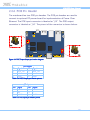
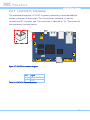
USER MANUAL VAB-820 Pico-ITX Freescale Cortex-A9 board 1.01-10252013-143200 Copyright Copyright © 2013 VIA Technologies Incorporated. All rights reserved. No part of this document may be reproduced, transmitted, transcribed, stored in a retrieval system, or translated into any language, in any form or by any means, electronic, mechanical, magnetic, optical, chemical, manual or otherwise without the prior written permission of VIA Technologies, Incorporated. Trademarks All trademarks are the property of their respective holders. Disclaimer No license is granted, implied or otherwise, under any patent or patent rights of VIA Technologies. VIA Technologies makes no warranties, implied or otherwise, in regard to this document and to the products described in this document. The information provided in this document is believed to be accurate and reliable as of the publication date of this document. However, VIA Technologies assumes no responsibility for the use or misuse of the information (including use or connection of extra device/equipment/add-on card) in this document and for any patent infringements that may arise from the use of this document. The information and product specifications within this document are subject to change at any time, without notice and without obligation to notify any person of such change. VIA Technologies, Inc. reserves the right the make changes to the products described in this manual at any time without prior notice. Regulatory Compliance FCCFCC-A Radio Frequency Interference Statement This equipment has been tested and found to comply with the limits for a class A digital device, pursuant to part 15 of the FCC rules. These limits are designed to provide reasonable protection against harmful interference when the equipment is operated in a commercial environment. This equipment generates, uses, and can radiate radio frequency energy and, if not installed and used in accordance with the instruction manual, may cause harmful interference to radio communications. Operation of this equipment in a residential area is likely to cause harmful interference, in which case the user will be required to correct the interference at his personal expense. Notice 1 The changes or modifications not expressly approved by the party responsible for compliance could void the user's authority to operate the equipment. Notice 2 Shielded interface cables and A.C. power cord, if any, must be used in order to comply with the emission limits. Notice 3 The product described in this document is designed for general use, VIA Technologies assumes no responsibility for the conflicts or damages arising from incompatibility of the product. Check compatibility issue with your local sales representatives before placing an order. Tested To Comply With FCC Standards FOR HOME OR OFFICE USE Battery Recycling and Disposal Only use the appropriate battery specified for this product. Do not re-use, recharge, or reheat an old battery. Do not attempt to force open the battery. Do not discard used batteries with regular trash. Discard used batteries according to local regulations. Safety Precautions Always read the safety instructions carefully. Keep this User's Manual for future reference. All cautions and warnings on the equipment should be noted. Keep this equipment away from humidity. Lay this equipment on a reliable flat surface before setting it up. Make sure the voltage of the power source and adjust properly 110/220V before connecting the equipment to the power inlet. Place the power cord in such a way that people cannot step on it. Always unplug the power cord before inserting any add-on card or module. If any of the following situations arises, get the equipment checked by authorized service personnel: The power cord or plug is damaged. Liquid has penetrated into the equipment. The equipment has been exposed to moisture. The equipment has not worked well or you cannot get it work according to User's Manual. The equipment has dropped and damaged. The equipment has obvious sign of breakage. Do not leave this equipment in an environment unconditioned or in a storage temperature above 60°C (140°F). The equipment may be damaged. Do not leave this equipment in direct sunlight. Never pour any liquid into the opening. Liquid can cause damage or electrical shock. Do not place anything over the power cord. Do not cover the ventilation holes. The openings on the enclosure protect the equipment from overheating VABVAB-820 User Manual Box Contents and Ordering Information VABVAB-820 1 x VAB-820 embedded board (with Freescale i.MX ARM Cortex-A9) 1 x DC-in power cable 1 x Audio cable 1 x USB cable 1 x COM cable (3-wired for the debug of console) iv VABVAB-820 User Manual Table of Contents 1. Product Overview ................................................................ ................................................................................................ ................................................................ 9 1.1. Key Features................................................................................................. 10 1.2. Product Specifications............................................................................... 11 1.3. Layout Diagram ........................................................................................... 14 1.4. Product Dimensions................................................................................... 16 1.5. Height Distribution..................................................................................... 17 2. I/O Interface................................ Interface................................................................ ................................................................................................ ........................................................................ ........................................ 18 2.1. External I/O Ports ....................................................................................... 18 2.1.1. RJ-45 LAN port: Gigabit Ethernet...................................................... 19 2.1.2. USB 2.0 Port ........................................................................................... 20 2.1.3. HDMI® Port............................................................................................. 21 2.1.4. RCA Jack.................................................................................................. 22 2.1.5. Micro SD Card slot ............................................................................... 23 2.2. Onboard Connectors ................................................................................ 24 2.2.1. USB, USBOTG Pin Header .................................................................. 24 2.2.2. Front Audio Pin Header....................................................................... 25 2.2.3. DIO, I²C, System reset, P_LED, and WLAN_LED Pin Header .... 26 2.2.4. CMOS Battery Connector.................................................................... 28 2.2.5. SPI connector ......................................................................................... 29 2.2.6. POE Pin Header..................................................................................... 30 2.2.7. +12V DC-In Connector........................................................................ 31 2.2.8. S-Video Input Pin Header ................................................................... 32 2.2.9. Mini-PCIe Slot ........................................................................................ 33 2.2.10. LVDS1 Connector ................................................................................. 35 2.2.11. LVDS Inverter Connector .................................................................... 37 2.2.12. MIPI CSI-2 Connector........................................................................... 38 2.2.13. COM1/COM2/CAN Connector.......................................................... 39 3. Jumpers ................................................................ ................................................................................................ ............................................................................... ............................................... 40 v VABVAB-820 User Manual 3.1. 3.2. 4. LVDS Power Select Jumper ..................................................................... 40 Boot Select Jumper.................................................................................... 42 Hardware Installation ................................................................ ........................................................................................ ........................................................ 43 4.1. Installing into a Chassis............................................................................. 43 4.1.1. Suggested minimum chassis dimensions ......................................... 43 4.1.2. Suggested minimum chassis height................................................... 45 4.1.3. Suggested keepout areas .................................................................... 46 4.2. Installation of Mini-PCIe module............................................................ 47 Appendix A. Mating Connector Vendor Lists ......................................................... ......................................................... 49 vi VABVAB-820 User Manual Lists of Figures Figure 1: Layout diagram of the VAB-820 mainboard (top and bottom view) . 14 Figure 2: Mounting holes and dimensions of the VAB-820................................... 16 Figure 3: Height distribution of the VAB-820 mainboard ...................................... 17 Figure 4: Rear I/O ports.................................................................................................. 18 Figure 5: Front I/O port .................................................................................................. 18 Figure 6: Gigabit Ethernet port pinout diagram ....................................................... 19 Figure 7: USB 2.0 port diagram .................................................................................... 20 Figure 8: HDMI® port diagram...................................................................................... 21 Figure 9: RCA jack diagram ........................................................................................... 22 Figure 10: Micro SD card slot diagram....................................................................... 23 Figure 11: USB, USBOTG pin header diagram .......................................................... 24 Figure 12: Front Audio pin header diagram .............................................................. 25 Figure 13: DIO, I²C, System reset, P_LED, and WLAN_LED combination pin header diagram ................................................................................................................ 26 Figure 14: CMOS battery connector diagram ........................................................... 28 Figure 15: SPI connector diagram ................................................................................ 29 Figure 16: POE Output/Input pin header diagram................................................... 30 Figure 17: 12V DC-In connector diagram .................................................................. 31 Figure 18: S-Video input pin header diagram ........................................................... 32 Figure 19: Mini-PCIe slot diagram................................................................................ 33 Figure 20: LVDS1 connector diagram ......................................................................... 35 Figure 21: LVDS Inverter Connector diagram ........................................................... 37 Figure 22: MIPI CSI-2 connector diagram................................................................... 38 Figure 23: COM1/COM2/CAN connector diagram ................................................. 39 Figure 24: LVDS power select jumper diagram........................................................ 40 Figure 25: Boot Select jumper diagram...................................................................... 42 Figure 26: Suggested minimum chassis dimensions ................................................ 43 Figure 27: Suggested minimum internal chassis ceiling height............................. 45 Figure 28: Suggested keepout areas ........................................................................... 46 vii VABVAB-820 User Manual Lists of Tables Table 1: Layout diagram description table of the VAB-820 mainboard ............ 15 Table 2: Layout diagram description table of rear I/O ports ................................ 18 Table 3: Gigabit Ethernet port pinout ........................................................................ 19 Table 4: Gigabit Ethernet LED color definition ........................................................ 19 Table 5: USB 2.0 port pinout........................................................................................ 20 Table 6: HDMI® port pinout ......................................................................................... 21 Table 7: RCA Jack pinout .............................................................................................. 22 Table 8: Micro SD card slot pinout............................................................................. 23 Table 9: USB, USBOTG pin header pinout................................................................ 24 Table 10: Front Audio pin header pinout.................................................................. 25 Table 11: DIO, I²C, System reset, P_LED, and WLAN_LED pin header pinout 27 Table 12: CMOS battery connector pinout .............................................................. 28 Table 13: SPI connector pinout ................................................................................... 29 Table 14: POE Output pin header pinout ................................................................. 30 Table 15: POE Input pin header pinout ..................................................................... 30 Table 16: 12V DC-In connector pinout...................................................................... 31 Table 17: S-Video input pin header pinout .............................................................. 32 Table 18: Mini-PCIe slot pinout ................................................................................... 34 Table 19: LVDS1 connector pinout............................................................................. 36 Table 20: LVDS Inverter Connector pinout............................................................... 37 Table 21: MIPI CSI-2 connector pinout ...................................................................... 38 Table 22: COM1/COM2/CAN connector pinout..................................................... 39 Table 23: LVDS power select jumper setting........................................................... 41 Table 24: Boot Select jumper settings ....................................................................... 42 Table 25: VAB-820 mating connector vendor lists ................................................. 49 viii VABVAB-820 User Manual 1. Product Overview Overview Based on the ultra compact Pico-ITX form factor, measuring 10 cm x 7.2 cm, the VIA VAB-820 is a VIA Pico-ITX board to feature an ARM SoC. With a 1.0GHz Freescale Cortex-A9 ARM SoC, the VIA VAB-820 combines three independent, integrated GPUs for 3D/2D graphics acceleration and supports multiple displays. The ultra compact VIA VAB-820 Pico-ITX is optimized for both performance and power to meet the high end demands of advanced industrial and invehicle applications, boasting a ruggedized design with an extended operating temperature range from -20 to 70°C, while offering extremely low power consumption. The VIA VAB-820 provides an impressive selection of rear I/O in a compact form factor including HDMI® port, two USB 2.0 ports, one composite input RCA jack and one RJ-45 GLAN port. Customers can take advantage of VIA’s industry leading hardware and software support to create customized designs with a quick time to market. The VIA VAB-820 is also available with board support packages (BSP) for the Android 4.2.2 and Embedded Linux 3.0.35 operating systems. On board pin headers provide support for an additional of two COM connectors with power supply, one dual-channel LVDS connector, one RTC battery connector, one micro SD card slot, one Mini-PCIe connector, one MIPI CSI-2 connector and eight GPIO pin headers, etc. 9 VABVAB-820 User Manual 1.1. Key Features Supports independent, integrated graphics processing (GPU) for 3D/2D and graphics acceleration and multiple displays Supports HDMI® port, RJ-45 LAN port and composite input RCA jack Supports four USB 2.0 ports (two as pin header) Supports one dual-channel 18/24-bit LVDS connector Supports two COM connectors with power supply Supports two Controller Area Network (FlexCAN) Small form factor and low power design Fanless and ultra low power consumption 4GB onboard eMMC Flash memory Support Mini-PCIe x1 connector and Micro SD card slot for expandable storage Compatible with Android 4.2.2 and Embedded Linux 3.0.35 10 VABVAB-820 User Manual 1.2. Product Specifications Processor Freescale i.MX 6Dual/6Quad ARM Cortex-A9 @ 1.0 GHz Flash Storage 4MB SPI Serial Flash 4GB eMMC Flash Graphics ® Support three independent, integrated graphics processing units: an OpenGL ES 2.0 3D graphics accelerator with four shaders (up to 200 MT/s and OpenCL support), 2D graphics accelerator, and dedicated OpenVG™ 1.1 accelerator System Memory Onboard 1GB DDR3-1066 SDRAM using 128M x16 memory devices (up to 2GB with 256M x 16 devices) Ethernet Micrel KSZ9031RNXIA Gigabit Ethernet Transceiver with RGMII Support Audio Freescale SGTL5000 Low Power Stereo Codec Video Decoder ADI ADV7180 8-Bit, 4× Oversampling SDTV Video Decoder HDMI Integrated HDMI 1.4 Transmitter USB SMSC USB2514 USB 2.0 High Speed 4-Port Hub Controllers Onboard I/O 2 X COM connectors with power supply (one supports 8-wire, while the other supports 2-wire, CAN1 and CAN2) 1 X Dual-channel, 18/24-bit LVDS connector 1 X RTC battery connector 1 X MIPI CSI-2 connector (supports 2 data lanes) 1 x LVDS panel connector 11 VABVAB-820 User Manual 1 x LVDS Inverter connector 1 x LVDS panel power select jumper 1 X SPI connector 1 X S-Video input pin header 2 X POE pin headers (support optional PD power board) 1 X Front audio pin header for line-in, line-out and MIC-in 1 X Boot select jumper (for SPI or micro SD) 1 X USB and USB OTG pin header 1 X 1 x DIO, I²C, System reset, Power LED, and WLAN LED pin header 1 X 12V DC-in power connector 1 X Mini-PCIe slot (supports multiple connections and buses including JTAG) Front Panel I/O 1 X Micro SD card slot Back Panel I/O 1 X HDMI port 2 X USB 2.0 ports 1 X RJ-45 LAN port (supports optional IEEE802.3at Type 2) 1 X Composite input RCA jack WatchDog Timer The Watchdog Timer supports two comparison points during each counting period. Each of the comparison points is configurable to evoke an interrupt to the ARM core, and a second point evokes an external event on the WDOG line Power 12VDC Operating System Embedded Linux 3.0.35 Android 4.2.2 Operating Conditions Operating Temperature -20°C ~ 70°C Operating Humidity 0% ~ 95% (relative humidity; non-condensing) Stor Storage age Temperature -40°C ~ 70°C 12 VABVAB-820 User Manual Form Factor 8-layers PCB 10 cm x 7.2 cm Note: 1. For the software evaluation, please visit VIA Embedded website to download the image: http://www.viaembedded.com/en/downloads/EvaluationKit.jsp aembedded.com/en/downloads/EvaluationKit.jsp http://www.vi 2. After the VAB-820 is shut down, it remains in stand by mode so that some components may retain power. If user has concern about power consumption during shut down, it is recommended to directly unplug the AC adapter from the board. 13 VABVAB-820 User Manual 1.3. Layout Diagram Figure 1: Layout diagram of the VABVAB-820 mainboard (top and bottom view) 14 VABVAB-820 User Manual Item Description 1 +12V DC-In connector (J9) 2 S-VIDEO input pin header (S-VIDEO1) 3 LVDS power select jumper (J3) 4 Freescale i.MX 6Dual/6Quad ARM Cortex-A9 processor 5 CMOS Battery connector (J1) 6 eMMC Flash 7 POE Input pin header (J13) 8 DIO, I²C, System reset, Power LED, and WLAN LED combination pin 9 Micro SD card slot 10 Boot flash Select jumper (J11) 11 USB and USBOTG combination pin header (J8) 12 Front Audio pin header (AUDIO1) 13 SPI connector (J10) 14 DDR3 1066 SDRAM memory 15 POE Output pin header (J14) 16 LVDS panel connector (LVDS1) 17 LVDS Inverter connector (INVERTER) 18 COM2/CAN connector (J5) 19 DDR3 1066 SDRAM memory 20 Mini-PCIe slot (MINIPCIE) 21 COM1 connector (J4) 22 MIPI CSI-2 connector (J18) header (J7) Table 1: Layout diagram description table of the VABVAB-820 mainboard 15 VABVAB-820 User Manual 1.4. Product Dimensions Figure 2: Mounting holes and dimensions of the VABVAB-820 16 VABVAB-820 User Manual 1.5. Height Distribution Figure 3: Height distribution of the VABVAB-820 mainboard 17 VABVAB-820 User Manual 2. I/O Interface The VAB-820 has a wide selection of interfaces. It includes a selection of frequently used ports as part of the external I/O coastline. 2.1. External I/O Ports Figure 4: Rear I/O ports Figure 5: Front I/O port Item Description 1 J16: RJ-45 LAN port 2 USB1: USB 2.0 port 2 3 USB0: USB 2.0 port 1 4 HDMI1: HDMI® port 5 6 J15: Composite input RCA jack Micro SD card slot Table 2: Layout diagram description table of rear I/O ports 18 VABVAB-820 User Manual 2.1.1. RJ-45 LAN port: Gigabit Ethernet The integrated 8-pin Gigabit Ethernet port is using an 8 Position 8 Contact (8P8C) receptacle connector (commonly referred to as RJ45). The pinout of the Gigabit Ethernet port is as shown below. Pin Signal 1 Signal pair 1+ 2 Signal pair 1- 3 Signal pair 2+ 4 Signal pair 3+ 5 Signal pair 3- 6 Signal pair 2- 7 Signal pair 4+ 8 Signal pair 4- Table 3: Gigabit Ethernet port pinout Figure 6: Gigabit Ethernet port pinout diagram The Gigabit Ethernet port (RJ45 port) has two individual LED indicators located on the front side to show its Active/Link status and Speed status. Link LED (Left LED on RJRJ-45 connector) Link Off Active LED (Right LED on RJRJ-45 connector) Off Off Speed_10Mbit The LED is always On in Orange color Flash in Yellow color Speed_100Mbit The LED is always On in Orange color Flash in Yellow color Speed_1000Mbit The LED is always On in Orange color Flash in Yellow color Table 4: Gigabit Ethernet LED color definition definition 19 VABVAB-820 User Manual 2.1.2. USB 2.0 Port The VAB-820 mainboard provides two USB 2.0 ports, Each USB port gives complete Plug and Play and hot swap capability for external devices. The USB interface complies with USB UHCI, Rev. 2.0. The pinout of the typical USB 2.0 port is shown below. 4 3 1 2 Figure 7: USB 2.0 port diagram USB1 USB2 Pin Signal Pin 1 VCC 1 Signal VCC 2 USB data - 2 USB data - 3 USB data + 3 USB data + 4 GND 4 GND Table 5: USB 2.0 port pinout 20 VABVAB-820 User Manual ® 2.1.3. HDMI Port The integrated 19-pin HDMI® port uses an HDMI® Type A receptacle connector defined in HDMI specification. The HDMI® port is used to connect high definition video and digital audio using a single cable. It allows connecting the digital video devices which utilize a high definition video signal. The pinout of the HDMI® port is shown below. Figure 8: HDMI® port diagram Pin Signal Pin Signal 1 TMDS Data0+ 2 GND 3 TMDS Data0– 4 TMDS Data1+ 5 GND 6 TMDS Data1– 7 TMDS Data2+ 8 GND 9 TMDS Data2– 10 TMDS Data3+ 11 GND 12 TMDS Data3– 13 CEC 14 NC 15 HDMI Clock 16 HDMI Data 17 GND 18 HDMI Power 19 Hot Plug Detect Table 6: HDMI® port pinout 21 VABVAB-820 User Manual 2.1.4. RCA Jack The RCA jack connects to external composite video input device. Figure 9: RCA jack diagram Description Video RCA Jack Composite Video Input Table 7: RCA Jack pinout 22 VABVAB-820 User Manual 2.1.5. Micro SD Card slot The VAB-820 comes with a Micro SD card slot located at the front side of the board. Micro SD card slot offers expandable storage. Figure 10: 10: Micro SD card slot diagram Pin Signal 1 SD0DATA2 2 SD0DATA3 3 SD0CMD 4 VDD (3.3V) 5 SD0CLK 6 GND 7 SD0DATA0 8 SD0DATA1 9 SD0_CD Table 8: Micro SD card slot pinout 23 VABVAB-820 User Manual 2.2. Onboard Connectors 2.2.1. USB, USBOTG Pin Header The mainboard includes one USB and USBOTG combination pin header block labeled as “J8”. The combination pin header is for connecting USB and USBOTG devices. The pinout of the pin header is shown below. Figure 11: 11: USB, USBOTG pin header diagram Pin Signal Pin Signal 1 GND 2 - 3 USB_OTG_ID 4 GND 5 OTG_DP 6 USBD_T3+ 7 OTG_DN 8 USBD_T3- 9 OTG_VBUS 10 USB_VBUS Table 9: USB, USBOTG pin header pinout 24 VABVAB-820 User Manual 2.2.2. Front Audio Pin Header The mainboard has a pin header for Line-out, Line-in and MIC-in. The pin header is labeled as “AUDIO1”. The pinout of the pin header is shown below. Figure 12: 12: Front Audio pin header diagram Pin Signal Pin Signal 1 HEAD_RIGHT 2 HEAD_LEFT 3 LINE_IN_R 4 LINE_IN_L 5 MIC_IN 6 MIC_IN 7 - 8 NC 9 GND_ANALOG 10 GND_ANALOG Table 10: 10: Front Audio pin header pinout 25 VABVAB-820 User Manual 2.2.3. DIO, I²C, System reset, P_LED, and WLAN_LED Pin Header The mainboard includes one DIO, I²C, System reset, P_LED, and WLAN_LED combination pin header block labeled as “J7”. The combination pin header is for connecting Digital I/O (GPIO), I²C devices and providing access to system reset switch, power LED and WLAN LED. The pinout of the pin header is shown below. Figure 13: 13: DIO, DIO, I²C, System reset, P_LED, and WLAN_LED combination pin header diagram 26 VABVAB-820 User Manual Pin Signal Pin Signal 1 RESET_N 2 P_LED+ 3 GND 4 P_LED- 5 12C3_SCL 6 W_LED+ 7 12C3_SDA 8 W_LED- 9 5VIN 10 GND 11 GPIO_1 12 GPIO_7 13 GPIO_2 14 GPIO_8 15 GPIO_4 16 GPIO_9 17 GPIO_5 18 GPIO_16 19 GND 20 - Table 11: 11: DIO, DIO, I²C, System reset, P_LED, and WLAN_LED WLAN_LED pin header pinout 27 VABVAB-820 User Manual 2.2.4. CMOS Battery Connector The mainboard is equipped with onboard CMOS battery connector used for connecting the external cable battery that provides power to the CMOS RAM. If disconnected all configurations in the CMOS RAM will be reset to factory defaults. The CMOS battery connector is labeled as “J1”. The connector pinout is shown below. Figure 14: 14: CMOS battery connector diagram Pin Signal 1 +VBAT 2 GND Table 12: 12: CMOS battery connector connector pinout 28 VABVAB-820 User Manual 2.2.5. SPI connector The mainboard has one 7-pin SPI flash connector. The SPI (Serial Peripheral Interface) connector is used to communicate with external slave devices. The connector is labeled as “J10”. The pinout of the connector is shown below. Figure 15: 15: SPI connect connector diagram Pin Signal 1 CSPI3_CLK 2 CSPI3_MOSI 3 CSPI3_MISO 4 3P3V 5 CSPI3_CS0 6 GND 7 CSPI3_CS1 Table 13: 13: SPI SPI connector connector pinout 29 VABVAB-820 User Manual 2.2.6. POE Pin Header The mainboard has two POE pin headers. The POE pin headers are used to connect to optional PD power board for implementation of Power Over Ethernet. The POE input connector is labeled as “J13”. The POE output connector is labeled as “J14”. The pinout of the connector is shown below. Figure 16: 16: POE Output/Input pin header diagram J14: Output Pin Signal Pin Signal 1 POE_12V 2 POE_12V 3 NC 4 - 5 GND 6 GND Table 14: 14: POE Output pin header pinout J13 J13: Input Input Pin Signal Pin Signal 1 WIRE1 2 WIRE2 3 NC 4 - 5 WIRE3 6 WIRE4 Table 15: 15: POE Input pin header pinout 30 VABVAB-820 User Manual 2.2.7. +12V DC-In Connector The mainboard supports +12V DC-In power connector to provide addition power to the rest of the system. The 2-pin power connector is used to connect the DC-In power jack. The connector is labeled as “J9”. The pinout of the connector is shown below. Figure 17: 17: 12V DCDC-In connector diagram Pin Signal 1 +12V 2 GND Table 16: 16: 12V DCDC-In connector pinout 31 VABVAB-820 User Manual 2.2.8. S-Video Input Pin Header The mainboard provides an S-Video Input pin header. The S-Video Input pin header is an analog video connector for connecting TV monitor or S-Video input devices. The pinout of the S-Video input pin header is shown below Figure 18: 18: S-Video input pin header diagram Pin Signal Pin Signal 1 C 2 GND 3 Y 4 - 5 NC 6 GND Table 17: 17: S-Video input pin header pinout 32 VABVAB-820 User Manual 2.2.9. Mini-PCIe Slot The Mini-PCIe slot is compatible with all PCIe 2.0 Mini Cards: full-length and half-length. The location of the Mini-PCIe slot is shown below. Figure 19: 19: MiniMini-PCIe slot diagram 33 VABVAB-820 User Manual Pin Signal Pin Signal 1 PCIE_WAKE_B 2 MPCIE_3V3 3 GND 4 GND 5 JTAG_TCK 6 VCC15 7 JTAG_TMS 8 - 9 GND 10 NC 11 PCIe_CREFCLKM 12 NC 13 PCIe_CREFCLKP 14 NC 15 GND 16 - 17 JTAG_TD1 18 GND 19 JTAG_TD0 20 PCIE_DIS_B 21 GND 22 PCIE_RST_B 23 PCIe_CRXM 24 MPCIE_3V3 25 PCIe_CRXP 26 GND 27 GND 28 VCC15 29 GND 30 PCIe_SMB_CLK 31 PCIe_CTXM 32 PCIe_SMB_DATA 33 PCIe_CTXP 34 GND 35 GND 36 PCIE_USB_DM 37 GND 38 PCIE_USB_DP 39 MPCIE_3V3 40 GND 41 MPCIE_3V3 42 LED_WWAN_B 43 GND 44 LED_WLAN_B 45 JTAG_nTRST 46 LED_WPAN_B 47 JTAG_nSRST 48 VCC15 49 GND 50 GND 51 NC 52 MPCIE_3V3 Table 18: 18: MiniMini-PCIe slot pinout 34 VABVAB-820 User Manual 2.2.10. LVDS1 Connector The mainboard has one 40-pin LVDS panel connector on the bottom side. The onboard LVDS panel connector allows to connect the panel’s LVDS cable to support the dual-channel 18-bit/24-bit display. Backlight controls are integrated into the LVDS panel connector pinout. The LVDS panel connector is labeled as “LVDS1”. The pinout of the connector is shown below. Figure 20: 20: LVDS1 connector diagram 35 VABVAB-820 User Manual Pin Signal Pin Signal 1 LVDS1_TX0_NC 2 PVDD 3 LVDS1_TX0_PC 4 PVDD 5 GND 6 GND 7 LVDS1_TX1_NC 8 GND 9 LVDS1_TX1_PC 10 LVDS0_TX0_NC 11 GND 12 LVDS0_TX0_PC 13 LVDS1_TX2_NC 14 GND 15 LVDS1_TX2_PC 16 LVDS0_TX1_NC 17 GND 18 LVDS0_TX1_PC 19 LVDS1_CLK_NC 20 GND 21 LVDS1_CLK_PC 22 LVDS0_TX2_NC 23 GND 24 LVDS0_TX2_PC 25 LVDS1_TX3_NC 26 GND 27 LVDS1_TX3_PC 28 LVDS0_CLK_NC 29 GND 30 LVDS0_CLK_PC 31 5VIN 32 GND 33 3P3V 34 LVDS0_TX3_NC 35 NC 36 LVDS0_TX3_PC 37 NC 38 LVDS0_EDID_SCL 39 NC 40 LVDS0_EDID_SDA Table 19: 19: LVDS1 LVDS1 connector pinout 36 VABVAB-820 User Manual 2.2.11. LVDS Inverter Connector The mainboard provides LVDS Inverter connector located on the bottom side of the board for supplying power to the backlight of the LCD panel. The connector is labeled as “INVERTER”. The pinout of the connector is shown below. Figure 21: 21: LVDS Inverter Inverter Connector diagram Pin Signal 1 IVDD 2 IVDD 3 LVDS_EN 4 DISP0_CONTRAST 5 LVDS_EN 6 DISP0_CONTRAST 7 GND 8 GND Table 20: 20: LVDS Inverter Inverter Connector pinout 37 VABVAB-820 User Manual 2.2.12. MIPI CSI-2 Connector The mainboard includes one MIPI CSI-2 connector on the bottom side of VAB820. The MIPI CSI-2 connector is used to connect to camera serial interface in order to support a wide range of imaging solutions. The connector is labeled as “J18”. The pinout of the connector is shown below. Figure 22: 22: MIPI CSICSI-2 connector diagram Pin Signal 1 5VIN 2 12C2_SCL 3 12C2_SDA 4 GND 5 CSI_CLK0P 6 CSI_CLK0M 7 GND 8 CSI_D0P 9 CSI_D0M 10 GND 11 CSI_D1M 12 CSI_D1P Table 21: 21: MIPI CSICSI-2 connector pinout 38 VABVAB-820 User Manual 2.2.13. COM1/COM2/CAN Connector The mainboard includes two onboard COM connectors on the bottom side of VAB-820. The onboard COM1 connector labeled as “J4” is used to attach additional COM port that support RS-232 standard with DTE (Data Terminal Equipment) type. The onboard COM2/CAN connector labeled as “J5” is primarily used to attach additional COM port for debug purpose. The CAN bus can also be supported through this connector. The pinout of COM/CAN connector is shown below. Figure 23: 23: COM1/COM2 COM1/COM2/CAN /COM2/CAN connector diagram COM1 COM2/CAN COM2/CAN Pin Signal Pin Signal 1 5VIN 1 5VIN 2 COM_RXD1 2 COM2_RX 3 COM_TXD1 3 COM2_TX 4 COM_DCD1 4 NC 5 COM_RI1 5 NC 6 GND 6 GND 7 COM_DTR1 7 CAN_RX2 8 COM_CTS1 8 CAN_TX2 9 COM_RTS1 9 CAN_TX1 10 COM_DSR1 10 CAN_RX1 Table 22: 22: COM1/COM2 COM1/COM2/CAN /COM2/CAN connector pinout Note: For CAN bus communication, the physical bus requires an external transceiver to make the transfer. 39 VABVAB-820 User Manual 3. Jumpers 3.1. LVDS Power Select Jumper The mainboard has power select connector that determines the input voltage for the LVDS connector (LVDS1) and LVDS inverter (INVERTER1). The pins 1, 3, and 5 correspond to INVERTER1. The Pins 2, 4, and 6 correspond to LVDS1. The jumper is labeled as “J3” .The jumper settings are shown below. Figure 24: 24: LVDS power select jumper diagram 40 VABVAB-820 User Manual Inverter power Pin 1 Pin 3 Pin 5 +12V (default) On On Off +5V Off On On LVDS power Pin 2 Pin 4 Pin 6 +3.3V (default) On On Off +5V Off On On Table 23: 23: LVDS power select jumper setting 41 VABVAB-820 User Manual 3.2. Boot Select Jumper The Boots Select jumper labeled as “J11” is to specify the boot device. Figure 25: 25: Boot Select jumper diagram J11: 11: Boot Select 1-2 3-4 ★Micro-SD (default) short open SPI open short Table 24: 24: Boot Select jumper settings 42 VABVAB-820 User Manual 4. Hardware Installation 4.1. Installing into a Chassis The VAB-820 can be fitted into any chassis that has the mounting holes compatible with the standard Pico-ITX mounting hole locations. Additionally, the chassis must meet the minimum height requirements for specified areas of the mainboard. 4.1.1. Suggested minimum chassis dimensions The figure below shows the suggested minimum space requirements that a chassis should have in order to work well with the VAB-820. Figure 26: 26: Suggested minimum chassis dimensions Each side of the mainboard should have a buffer zone from the internal wall of the chassis. The side of the mainboard that accommodates the I/O coastline should have a buffer of 1.00 mm. The side on the opposite end of the I/O 43 VABVAB-820 User Manual coastline should have a buffer of at least 4.00 mm. The two sides adjacent to the I/O coastline should have at least a 10.00 mm buffer. 44 VABVAB-820 User Manual 4.1.2. Suggested minimum chassis height The figure below shows the suggested minimum height requirements for the internal space of the chassis. It is not necessary for the internal ceiling to be evenly flat. What is required is that the internal ceiling height must be strictly observed for each section that is highlighted. Figure 27: 27: Suggested minimum internal chassis ceiling height 45 VABVAB-820 User Manual 4.1.3. Suggested keepout areas The figure below shows the areas of the mainboard that is highly suggested to leave unobstructed. Figure 28: 28: Suggested keepout areas 46 VABVAB-820 User Manual 4.2. Installation of Mini-PCIe module Step 1 Align the notch on the Mini-PCIe module with the notch on the Mini-PCIe slot then insert the module at 30° angle. 47 VABVAB-820 User Manual Step 2 Once the module has been fully inserted, push down the module until the screw holes align with the mounting holes on the hex spacer screws. Secure the module with two screws to the standoffs. 48 VABVAB-820 User Manual Appendix A. Mating Connector Vendor Lists The following table listed the mating connector vendors of VAB-820 mainboard. Connectors Vendor & P/N J1 99G30-170512 INVERTER LVDS1 J10 99G30-170542 99G30-170152 99G30-170852 Mating Vendor & P/N ACES MOLEX 85206-0200 51021-**00 ACES MOLEX 85206-0800 51021-**00 ACES HRS 44002-4000 DF13-**DS-1.258C ACES 87214-0700 J4 & J5 99G30-021457 ACES 87214-1000 J18 99G30-170642 ACES 87214-1000 S-VIDEO1 99G30-05474I AUDIO1 99G30-05454I J8 99G30-05380I J7 99G30-05301I J9 99G30-021525 J13, J14 99H30-05770K Neltron 2208S-XXG 2208R-XXG 2208SM-XXG SAMTEC SSW Series Neltron JST 2318HJ-02 XH Series Neltron SAMTEC SSW Series 2214S-XXG-85 2214R-XXG-85 Table 25: 25: VABVAB-820 mating connector vendor lists 49 Taiwan Headquarters USA Europe 1F, 531 Zhong-Zheng Road Xindian District, New Taipei City 231, Taiwan 940 Mission Court Fremont, CA 94539 USA In den Dauen 6 53117 Bonn Germany TEL: 886.2.2218.5452 FAX: 886.2.2218.5453 Email: [email protected] TEL: 1.510.683.3300 FAX: 1.510.687.4654 Email: [email protected] TEL: 49.228.688565.0 FAX: 49.228.688565.19 Email: [email protected] China Japan Korea Tsinghua Science Park Bldg. 7 No. 1 Zongguancun East Road Haiden District, Beijing, 100084 China 3-15-7 Ebisu MT Bldg. 6F Higashi, Shibuya-ku Tokyo 150-0011 Japan 2F, Sangjin Bldg., 417 Dogok Dong, Gangnam-Gu Seoul 135-854 South Korea TEL: 86.10.59852288 FAX: 86.10.59852299 Email: [email protected] TEL: 81.3.5466.1637 FAX: 81.3.5466.1638 Email: [email protected] TEL: 82.2.571.2986 FAX: 82.2.571.2987 Email: [email protected]