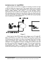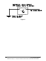
1
Not Recommended for New Installations.
Please contact Technical Support for more information.
Parallel Port Input/Output Converter
Model PPIO
Document No. PPIO2899
B&B Electronics Mfg. Co. Inc.
707 Dayton Road -- P.O. Box 1040 -- Ottawa, IL 61350 USA
Phone (815) 433-5100 -- General Fax (815) 433-5105
Home Page: www.bb-elec.com
Sales e-mail: [email protected] -- Fax (815) 433-5109
Technical Support e-mail: [email protected] -- Fax (815) 433-5104
Copyright ? 1991-1999 B&B Electronics -- Revised June 1999
.PPIO2899 Manual
Cover Page
B&B Electronics Mfg Co Inc – 707 Dayton Rd - PO Box 1040 - Ottawa IL 61350 - Ph 815-433-5100 - Fax 815-433-5104
TABLE OF CONTENTS
INTRODUCTION .............................................................................1
PACKING LIST.................................................................................2
PC PARALLEL PORT DESCRIPTION ...........................................3
PPIO DESCRIPTION & CONNECTION..........................................7
CONTROLLING THE PPIO USING GWBASIC..............................9
CONTROLLING THE PPIO USING PASCAL...............................12
CONTROLLING THE PPIO USING C...........................................18
INTERFACING TO THE PPIO.......................................................27
EXAMPLE USE OF THE PPIO .....................................................29
APPENDIX.....................................................................................33
HEXADECIMAL NUMBERS ..............................................................33
BINARY NUMBERS ........................................................................34
PPIO2899 Manual
Table of Contents
B&B Electronics Mfg Co Inc – 707 Dayton Rd - PO Box 1040 - Ottawa IL 61350 - Ph 815-433-5100 - Fax 815-433-5104
i
INTRODUCTION
The PPIO allows you to connect your IBM PC (or clone)
computer to the outside world using the computer’s parallel port.
The eight I/O points can be used as either inputs or outputs. As an
output they can control voltages as high as 50 Volts DC and can
handle currents as high as 500 mA DC. As an input they can handle
voltages from 0 to 50 volts with a threshold of 2.5 Volts DC.
CAUTION: Each output of the PPIO can dissipate 1 Watt when
used alone, however, all eight outputs together cannot
dissipate more than 2.25 Watts.
NOTE: The PPIO connects to the parallel port of your computer and
uses most of the available pins on that port. You MUST use a cable
that connects pins 1 through 17 of the DB-25 connector to the PPIO
for it to work properly. To be safe you should use a cable that
connects all 25 pins from connector to connector.
NOTE: The PPIO can only be used with parallel ports that are in
“compatible” or “normal” mode. It will not function properly with
parallel ports in ECP or EPP modes. The mode of the parallel port
can be changed in the BIOS setup by pressing either the F2 key or
DEL key just after the computer begins the boot procedure.
The PPIO comes with sample DOS programs written in
GWBASIC, QuickBASIC, Pascal, and C. These sample programs
can be used "as is" to test the PPIO and to control and display the
status of its I/O pins. Parts of these programs can be used in other
programs to make it easier to interface to the PPIO. Also, by
studying these programs a programmer can learn how to write code
in any language to do a similar job.
PPIO2899 Manual
B&B Electronics Mfg Co Inc – 707 Dayton Rd - PO Box 1040 - Ottawa IL 61350 - Ph 815-433-5100 - Fax 815-433-5104
1
Packing List
Examine the shipping carton and contents for physical damage.
If there is damage, contact B&B Electronics immediately. The
following items should be in the shipping carton:
1)
2)
3)
PPIO unit
This Instruction Manual
PPIO Sample/Test Disk
If any of the above items is missing contact B&B Electronics
immediately.
2
PPIO2899 Manual
B&B Electronics Mfg Co Inc – 707 Dayton Rd - PO Box 1040 - Ottawa IL 61350 - Ph 815-433-5100 - Fax 815-433-5104
PC PARALLEL PORT DESCRIPTION
To understand how the PPIO can be controlled you must
first understand how the parallel port works inside the computer. The
parallel port is designed to connect the computer with the outside
world. It can have up to 12 TTL compatible outputs and up to 9 TTL
compatible inputs. It cannot have both at the same time since some
inputs and outputs share pins. Eight of the outputs and five of the
inputs are dedicated. Four of the lines can be either inputs or
outputs.
The main use for the parallel port is to send data to a
printer. The port uses the eight dedicated outputs for data and the
other lines for handshakes. Under normal printer operation, the
computer will put an eight-bit byte on the eight lines (pins 2-9) and
then use the Strobe output (pin 1) to tell the printer to read the data.
Upon receipt of an Acknowledge (pin 10) from the printer the
computer knows that the eight bit word was received. It can then
send the next word. Other lines are used for busy, off line, etc.
All the control of the parallel port is done through software. If
you look at the hardware you find that the parallel port is connected
directly to the computer bus. This means that we can address these
inputs and outputs in any way we want if we do not use the port to
drive a printer.
Each PC has port addresses where the parallel ports, serial
ports, hard disk, etc. can be addressed. These are located in the
address range from 0000H to 03FFH (the H indicates the use of the
hexadecimal numbering system). Each parallel port has one main
port address for outputting data. The next two addresses above that
address are used for handshaking control. For instance, on a typical
computer a parallel port could be located at address 0378H. The
handshaking lines will then be located at 0379H and 037AH. Table 1
shows the correspondence between the bits of the port and the pins
of the DB-25 female connector.
Referring to Table 1, if you output a 01H (which is 00000001
in binary) to your computer’s port 0378H, then pin 2 of the parallel
port’s DB-25 connector will be HIGH and pins 3 through 9 will be
LOW. To do this using GWBASIC you would use the command:
OUT &H378,&H01. Using this method you can output any pattern
you wish on pins 2 through 9 of the parallel port. To turn ON pins 2,
4, 6, and 8 use: OUT &H378,&H55. 55H is the same as 01010101
binary. This port (0378H) can be read as an input, but mostly it is
PPIO2899 Manual
B&B Electronics Mfg Co Inc – 707 Dayton Rd - PO Box 1040 - Ottawa IL 61350 - Ph 815-433-5100 - Fax 815-433-5104
3
used to read the status of the port. The PPIO does not need to use
this port as an input port.
Again, referring to Table 1, if you input the data on port
0379H, then whatever TTL level pins 15, 13, 12, 10, and 11 are will
show up as bits 3 through 7. The state of bits 0, 1, and 2 will be
unknown since they are not hooked to anything, but they probably
will be HIGH (ONE). Note that the data on pin 11 will be inverted, if
pin 11 is LOW you will get a HIGH on bit 7. The pins with the “bars”
over them are all inverted. This is done by the hardware in the
parallel port over which we have no control. A way to read these pins
using GWBASIC is: A1=INP(&H379). A1 will then have the results of
the input from port address 0379H. Bit 3 of A1 will have the status of
pin 15, bit 4 the status of pin 13, etc.
Note that on the third address (037AH) the pins can be
either inputs or outputs. If you use the GWBASIC command OUT
&H37A,&H01 (00000001 BINARY) then pin 1 will be LOW (because
it is inverted), pins 14 and 17 will be HIGH (they also are inverted),
and pin 16 will be LOW (it is not inverted).
4
PPIO2899 Manual
B&B Electronics Mfg Co Inc – 707 Dayton Rd - PO Box 1040 - Ottawa IL 61350 - Ph 815-433-5100 - Fax 815-433-5104
378H
BIT
Output
379H
Input
Output
37AH
Input
Output
Input
_
1
_
14
_
1
_
14
16
_
17
See
Note 2
0
2
2
X
X
1
3
3
X
X
2
4
4
X
X
3
5
5
X
15
4
6
6
X
13
16
_
17
See
Note 2
5
7
7
X
12
X
X
6
8
8
X
X
X
7
9
9
X
10
_
11
X
X
Table 1
Note 1: X means no connection to any DB-25 pin.
Note 2: Bit 4 of 37AH as an output is used to control the interrupt IRQ7.
When this bit is HIGH, IRQ7 is enabled and when this bit is LOW, IRQ7 is
disabled. As an input, this reads the status of the IRQ7 interrupt to see if it
is enabled or not.
Note 3: The “bars” over the top of some pin numbers indicate that those
signals are inverted (in hardware) from PC's bus to DB-25 pin.
You can also read pins 1, 14, 16, and 17 using the INP(&H37A)
command. For this to work properly, you must first force all the
outputs HIGH. The way the parallel port is wired, if you do not force
the outputs HIGH they will interfere with the inputs. To do this, use
the command OUT &H37A,&H04 (04H is the same as 00000100
binary). Pins 1, 14, and 17 are inverting so a ZERO written to them
forces them HIGH. Pin 16 is non-inverting so the ONE written to it
forces it HIGH. After issuing the OUT command you can then do a
A2=INP(&H37A) that will read the TTL levels on those pins. In this
case the four upper bits (bits 4-7) will be unknown, but will probably
be HIGH.
PPIO2899 Manual
B&B Electronics Mfg Co Inc – 707 Dayton Rd - PO Box 1040 - Ottawa IL 61350 - Ph 815-433-5100 - Fax 815-433-5104
5
There are three port addresses that are normally used on a PC
for parallel ports: 3BCH, 378H, and 278H. When your PC is reset or
turned on these three addresses are scanned by the BIOS in the
order shown above. The first one that the BIOS finds with a parallel
port installed is assigned the logical name LPT1. The second, LPT2,
etc. You can connect the PPIO to a port located at any of these
three addresses. During power up the computer will assign that port
a logical name but we will ignore it and communicate to the port
directly.
If you are using a base address of 0278H the I/O port addresses
in Table 1 would change to 0278H, 0279H, and 027AH. With a base
address of 03BCH the addresses are 03BCH, 03BDH, and 03BEH.
Check your computer manual to find out which address your parallel
port has. It is also possible to purchase a special parallel port from
B&B Electronics that can be set at any address in the I/O port
address space from 0000H to 03FFH.
The above parallel port information is true for the vast majority of
the PC compatible ports. However, a few computer manufacturers
have chosen to make their parallel ports non-standard. On some
battery powered computers pins are disabled to save power. Some
ports may also have extra “direction control” bits. If you have
problems where one or more bits are always on or off you should
check your owner's manual. You may have to enable the port or set
the “direction bit” correctly to get the port to work with the PPIO. If a
pin is missing you may have to install a different parallel port card to
get the PPIO to work properly.
6
PPIO2899 Manual
B&B Electronics Mfg Co Inc – 707 Dayton Rd - PO Box 1040 - Ottawa IL 61350 - Ph 815-433-5100 - Fax 815-433-5104
PPIO DESCRIPTION & CONNECTION
The PPIO makes use of the eight output pins (pins 2 through 9)
at address 378H to drive its eight outputs. It uses the upper four bits
of address 379H (pins 13, 12, 10, and 11) for the upper four input
bits of the PPIO. It uses the lower four input bits of address 37AH
(pins 1, 14, 16, and 17) for the lower four input bits of the PPIO. This
assumes you are using the same port addresses as in Table 1. In
this way the PPIO can have eight inputs or eight outputs. Refer to
Figure 1 for the PPIO schematic.
Each pin of the PPIO is bi-directional. It can be used as either an
input or an output. Referring to Figure 1 you will see that PPIO bit 0
can be driven by pin 2 of the parallel port or it can be read by pin 1 of
the parallel port. The drivers are open collector Darlington
transistors that can sink up to 500 mA and are protected by “kick
back” diodes that are connected to the positive power supply. These
outputs can handle voltages as high as 50 Volts DC. If bit 0 of port
0378H is HIGH, pin 2 of the parallel port is HIGH and the PPIO
output pin will be LOW and can sink 500 ma. If bit 0 goes LOW, pin
2 will go LOW and the PPIO transistor will go OFF.
To use PPIO I/O bit 0 as an input you first set bit 0 of port 378H
LOW to turn OFF the driver transistor. From then on, if you force the
PPIO bit 0 to ground, a LOW will show up on pin 1 of the DB-25
connector. If you look at Table 1 you will note that pin 1 is inverting
in the computer parallel port. This means that a LOW on pin 1 will
show up as a HIGH in the computer. This is called negative true
logic. The PPIO receivers are set up as inverters or non-inverters to
compensate for the inverting and non-inverting inputs of the parallel
port.
All you have to remember is that if you force one of the PPIO I/O
bits to ground, it will be a ONE when you read it in the computer. If
you leave the PPIO I/O pin open or force it HIGH (above 2.5 volts), it
will be a ZERO when you read it in the computer.
PPIO I/O bits 0 through 3 are connected to bits 0 through 3 of
port 037AH and PPIO I/O bits 4 through 7 are connected to bits 4
through 7 of port 0379H. (This assumes that you are using a parallel
port at 0378H in your computer.) A LOW on any PPIO I/O pin will
show up as a HIGH on the corresponding bit in the computer.
PPIO2899 Manual
B&B Electronics Mfg Co Inc – 707 Dayton Rd - PO Box 1040 - Ottawa IL 61350 - Ph 815-433-5100 - Fax 815-433-5104
7
Figure 1
8
PPIO2899 Manual
B&B Electronics Mfg Co Inc – 707 Dayton Rd - PO Box 1040 - Ottawa IL 61350 - Ph 815-433-5100 - Fax 815-433-5104
CONTROLLING THE PPIO USING GWBASIC
Refer to the fragment of GWBASIC code in Figure 2 to see how
to input the bits and make one 8-bit word.
100 OUT &H37A,&H04:
120
140
160
180
200
.
.
REM This disables the 37AH Outputs
REM inside of the computer
REM so that we can use
REM 37AH as an input port.
REM It also disables
REM the IRQ7 interrupt.
300 A1=INP(&H37A) AND &H0F:
320
340
360
380
REM Input the
REM lower 4 bits
REM and mask OFF
REM (force to 0)
REM the upper 4 bits.
400 A2=INP(&H379) AND &HF0: REM Input the high 4 bits
420
REM and mask OFF
440
REM the lower 4 bits.
460 IB=A1 OR A2 :
480
.
.
REM This combines them
REM into one Input Byte.
Figure 2
The above assumes that you are using a parallel port located at
0378H. If you are using a different port you will have to replace the
hex addresses shown with the proper ones for your port. Refer also
to the PPIO.BAS program on the supplied disk for an example of
how to use GWBASIC to interface with the PPIO.
To output bits from the computer to the PPIO interface (still
using GWBASIC and the above 0378H example) use the following
line:
500 OUT &H378,OB
Where OB is the byte you want to output. If, for instance, you want
to turn ON (force LOW) PPIO bit 0, you must turn ON (force HIGH)
bit 1 of the variable OB. This can be done by ORing OB with &H01.
If you want to turn OFF (force HIGH or open) the same PPIO pin you
must turn OFF (force LOW) bit 1 of OB. Do this by ANDing OB with
NOT &H01. Use the data Table 2 to handle all eight PPIO bits.
PPIO2899 Manual
B&B Electronics Mfg Co Inc – 707 Dayton Rd - PO Box 1040 - Ottawa IL 61350 - Ph 815-433-5100 - Fax 815-433-5104
9
I/O Bit
0
1
2
3
4
5
6
7
Force I/O ON
(Low)
OR &H01
OR &H02
OR &H04
OR &H08
OR &H10
OR &H20
OR &H40
OR &H80
Table 2
Force I/O OFF
(High)
AND NOT &H01
AND NOT &H02
AND NOT &H04
AND NOT &H08
AND NOT &H10
AND NOT &H20
AND NOT &H40
AND NOT &H80
The big advantage of using the ANDing and ORing as shown in
Table 2 is that it makes each PPIO pin independent. If you have, for
instance, PPIO bit 2 ON and all of the rest of the bits OFF then your
variable OB will be equal to 04H (00000100 binary). PPIO bit 2 will
be LOW or ON. If you then want to turn ON bit 3 do the following:
500 OB=OB OR &H08
520 OUT &H378,OB
Bit 3 will go LOW and bit 2 will stay LOW. At that time OB will be
equal to &H0C (00001100 binary). To turn OFF bit 3 do the
following:
700 OB=OB AND NOT &H08
720 OUT &H378,OB
Bit 3 will go HIGH or open and bit 2 will stay LOW. By using the OR
and AND NOT commands in Table 2, bit 3 has been turned ON and
OFF without disturbing any of the other PPIO Bits.
You may also use the PPIO with some pins as inputs and some
pins as outputs. There can be any number of each and in any order.
Remember that before you can use a PPIO pin as an input you must
first force the output driver on that pin OFF by putting a ZERO on
that bit. For example suppose we want to use bits 0, 1, and 2 as
outputs and bits 3, 4, 5, 6, and 7 as inputs. We also want bit 1 to be
ON (or LOW) when we start the program. We need to turn OFF bits
3, 4, 5, 6, and 7 so we can use them as inputs and turn ON the
output bit 1. You should modify Figure 2 to add the following line:
180 OUT &H378,&H02
From then on you can use the first three lines of Table 2 to
control the three outputs and lines 220-320 of Figure 2 to input data.
10
PPIO2899 Manual
B&B Electronics Mfg Co Inc – 707 Dayton Rd - PO Box 1040 - Ottawa IL 61350 - Ph 815-433-5100 - Fax 815-433-5104
When you input the 8-bit word using lines 300-460 of Figure 2,
note that you also get the status of the outputs. If some I/O bits are
used by the PPIO as outputs the status of the bits you read will tell
you the status of the PPIO outputs. If PPIO output bit 0 is LOW then
bit 0 of IB (the variable InputByte) will be HIGH (1). This can be used
to check that the PPIO hardware is connected and is working
properly. If, through a fault, a PPIO bit is shorted to ground then,
when you read that bit it will be HIGH no matter what you output to
the PPIO bit. If there are no shorts or inputs that are LOW on the
PPIO pins then any byte you output should come back the same
when you input.
A good way to test for shorts is by outputting a &HAA (10101010
binary) and checking to see that the input is the same. Then output
a &H55 (01010101 binary) and check the input. This tests for both
pin-to-pin shorts and shorts to ground. At the same time this tests
that the PPIO is plugged in properly and you have the correct port
selected. This will not work if any of the PPIO pins are connected to
a device that is grounding or holding a pin LOW. If you have this
problem you will have to ignore these bits when you read the port.
NOTE: If the PPIO is connected properly and the upper four outputs
(4 - 7) are functional, but the lower four outputs (0 - 3) are not
functional, the parallel port may be in ECP or EPP mode. It must be
in “compatible” or “normal” mode for the PPIO to work properly. The
mode of the parallel port can be changed in the BIOS setup by
pressing either the F2 key or DEL key just after the computer begins
the boot procedure.
PPIO2899 Manual
B&B Electronics Mfg Co Inc – 707 Dayton Rd - PO Box 1040 - Ottawa IL 61350 - Ph 815-433-5100 - Fax 815-433-5104
11
CONTROLLING THE PPIO USING PASCAL
The PPIO disk includes two source code files as an example of
using the PPIO with the Pascal programming language. PPIO.PAS
is the main routine of the example program. PPIOUNIT.PAS
contains the routines for communicating with the PPIO. In the rest of
this section, we assume that you know the Pascal programming
language. Consult your reference manuals if you need help with the
language.
The Pascal Unit, PPIOUNIT.PAS handles communication with
the parallel port. It defines five variables. They are defined as:
Input_Byte
Output_Byte
Base_Address
Status_Address
Control_Address
: BYTE;
: BYTE;
: WORD;
: WORD;
: WORD;
{ Byte that’s read from PPIO }
{ Byte that’s written to PPIO }
{ Base address of Parallel Port }
{ Status Register Address }
{ Control Register Address }
No function outside the Unit can directly access these variables.
Functions outside the Unit call functions within the Unit to modify
and return the value of these variables.
The procedure Set_Start, sets the variable Base_Address,
Status_Address, Control_Address and Output_Byte. It also sets up
the initial state of the parallel port. The function is defined as:
PROCEDURE Set_Start(Address:WORD; Init:BYTE);
BEGIN
Base_Address
:= Address;
Status_Address
:= Base_address+1;
Control_Address
:= Base_Address+2;
PORT[Base_Address]:= Init;
Output_Byte
:= Init;
{Parallel Port Base Address}
{Parallel Port Status Address}
{Parallel Port Control Address}
{Write Init Value to Output Address}
{Put Init value In the Output_Byte Var}
END; {Set_Start}
This function must be the first one used, because all other functions
assume that the variables have been set.
The Procedure, Set_IRQ_OFF, tells the parallel port not to
generate any interrupts. This should be called immediately after
Set_Start. It is defined as:
12
PPIO2899 Manual
B&B Electronics Mfg Co Inc – 707 Dayton Rd - PO Box 1040 - Ottawa IL 61350 - Ph 815-433-5100 - Fax 815-433-5104
PROCEDURE Set_IRQ_Off;
BEGIN
PORT[Control_Address] := $04;{Write 4 to disable IRQ}
END; {Set_IRQ_Off}
The function, In_Byte, returns the value of the variable,
Input_Byte. It is defined as:
FUNCTION In_Byte : Byte;
BEGIN
In_Byte := Input_Byte;
End; { In_Byte }
Notice that this does not read the value of the parallel port. The
function Read_Input_Bit reads the port.
The function, Out_Byte, returns the value of the variable
Output_Byte. It is defined as:
FUNCTION Out_Byte : Byte;
BEGIN
Out_Byte := Output_Byte;
End; { Out_Byte }
Notice that this does not read the parallel port. It only returns the
value of Output_Byte.
The function, Read_Input_Bit, returns the status of the specified
input line. The function is defined as:
FUNCTION Read_Input_Bit (Bit_Number:BYTE) : BYTE;
BEGIN
Input_Byte := (PORT[Status_Address] AND $F0)
OR (PORT[Control_Address] AND $0F) ;
IF ( (Input_Byte AND (1 SHL Bit_Number) ) = 0 ) THEN
Read_Input_Bit := 0
ELSE
Read_Input_Bit := 1;
END; {Read_Input_Bit}
PPIO2899 Manual
B&B Electronics Mfg Co Inc – 707 Dayton Rd - PO Box 1040 - Ottawa IL 61350 - Ph 815-433-5100 - Fax 815-433-5104
13
The parallel port’s status register stores the upper nibble (four
bits) of the input line status. Since the smallest value that can be
read from the port is a byte, some work must be done to get only the
upper nibble’s value. We read a byte from the status register and
bitwise AND it with F0h (240 decimal, 11110000 binary). This sets
the lower nibble of the byte to zero.
The parallel port’s control register stores the low nibble of the
input line status. A method, similar to the one used to get the high
nibble, extracts the low nibble. We read a byte from the control
register and bitwise AND it with 0Fh (15 decimal, 00001111 binary).
This sets the upper nibble of the byte to zero.
Now, combine both bytes into one value by bitwise ORing them
together. This value is stored in the variable Input_Byte. At this point,
the upper nibble of Input_Byte is the same as the upper nibble of the
status register and the lower nibble of Input_Byte is the same as the
lower nibble of the control register.
To return the status of a specific line, a test is done to determine
the state of the line’s corresponding bit stored in Input_Byte. To
determine the bit’s state, all other bits of Input_Byte are set to zero.
This is done by bitwise ANDing Input_Byte with the mask value of
the desired line shown in the following table.
Mask Value
Line
0
1
2
3
4
5
6
7
14
Hex
01h
02h
04h
08h
10h
20h
40h
80h
Decimal
1
2
4
8
16
32
64
128
Binary
00000001
00000010
00000100
00001000
00010000
00100000
01000000
10000000
PPIO2899 Manual
B&B Electronics Mfg Co Inc – 707 Dayton Rd - PO Box 1040 - Ottawa IL 61350 - Ph 815-433-5100 - Fax 815-433-5104
Notice that in the binary representation of the mask value, line
zero’s mask has bit number zero set, and line one’s mask has bit
number one set, etc. So, instead of retrieving the mask value from a
table, the value is calculated by shifting 00000001b (1 decimal, 01
hexadecimal) right the same number of times as the desired line
number. Once the mask value is calculated, it is bitwise ANDed with
Input_Byte. If the resulting value is non-zero, the line is ON and a
boolean TRUE is returned, otherwise a boolean FALSE is returned.
For example:
Line_Number = 3
Status Register Value = 01010101b
Control Register Value = 10101010b
AND
AND
01010101b (Status Register)
11110000b (F0h mask)
01010000b
10101010b (Control Register)
00001111b (0Fh mask)
00001010b——> OR
00001010b
01011010b
00000001b (1 decimal)
shift-right 3(Line_Number)= AND
00001000b(bit mask)
00001000b
The function, Output_Bit, returns the status of the selected
output line. The function is defined as:
FUNCTION Output_Bit (Bit_Number:BYTE) : BYTE;
BEGIN
If ( ( Output_Byte AND (1 SHL Bit_Number ) ) = 0 THEN
Output_Bit : = 0
ELSE
Output_Bit : = 1;
END; {Output_Bit}
PPIO2899 Manual
B&B Electronics Mfg Co Inc – 707 Dayton Rd - PO Box 1040 - Ottawa IL 61350 - Ph 815-433-5100 - Fax 815-433-5104
15
As with the function, In_Byte, the mask value is calculated by
shifting 00000001b right the same number of times as the desired
line number. Once the mask value is calculated, it is bitwise ANDed
with Output_Byte. If the resulting value is non-zero, the line is ON
and a boolean TRUE is returned, otherwise a boolean FALSE is
returned. Notice that this function gets its value from Output_Byte
that is set when we use the function, Set_Output_Bit. The value is
not read from the port.
For example:
Line_Number = 3
Output_Byte = 10101010b
00000001b
shift-right 3 (Line_Number) =
AND
00001000b
10101010b (Output_Byte)
00001000b
The function, Set_Output_Bit, sets the selected output line ON of
OFF. The function is defined as:
PROCEDURE Set_Output_Bit ( Bit_Number,Output:BYTE ) ;
BEGIN
Output_Byte := ( (Output_Byte AND ( ( 1 SHL Bit_Number)
XOR $FF) ) OR (Output SHL Bit_Number) ) ;
Port [Base_Address] : = Output_Byte;
END; {Set_Output_Bit}
The variable, Output_Byte, stores the status of the output lines.
When a bit in Output_Byte is set to a one, its corresponding output
line is ON, when it is set to a zero, the line is OFF. To set a bit to the
specified status, the bit must first be cleared. To do this, 00000001b
is shifted right for the desired line number and bitwise exclusive
ORed with FFh (255 decimal, 11111111 binary) to produce a mask
value. This mask value has all bits set to one except for the desired
line. It is bitwise ANDed with Output_Byte to clear the desired bit.
Now, having cleared the bit, it can be set to the specified state.
Since the state is either a zero or one, we can shift it right for the
desired line number to get another mask value. This value is then
bitwise ORed with the cleared value to obtain the new value of
Output_Byte. The final step is to write Output_Byte to the parallel
port.
16
PPIO2899 Manual
B&B Electronics Mfg Co Inc – 707 Dayton Rd - PO Box 1040 - Ottawa IL 61350 - Ph 815-433-5100 - Fax 815-433-5104
For example:
Output_Byte
Line_Number
Status
= 01010101b
=3
=1
00000001b (1 decimal)
shift-right 3 (Line_Number) =
XOR
AND
00000001b (Status)
shift-right 3 (Line_Number) = OR
00001000b
11111111b
11110111b (mask 1)
01010101b (Output_Byte)
01010101b
00001000b (mask 2)
01011101b (New Output_Byte)
For an example of an application that uses these functions, look
at the source code in PPIO.PAS.
PPIO2899 Manual
B&B Electronics Mfg Co Inc – 707 Dayton Rd - PO Box 1040 - Ottawa IL 61350 - Ph 815-433-5100 - Fax 815-433-5104
17
CONTROLLING THE PPIO USING C
The PPIO disk includes three source code files as an example
of using the PPIO with the C programming language. PPIO.C is the
main routine of the example program. PPIOFUNC.C contains the
routines for communicating with the PPIO. PPIOFUNC.H contains
the function prototypes and definitions for use by PPIOFUNC.H and
PPIO.C. In the rest of this section, we assume that you know the C
programming language. Consult your reference manuals if you need
help with the language.
PPIOFUNC.H makes some definitions used in the rest of this
section.
#define Status_Address Base_Address+1
#define Control_Address Base_Address+2
typedef enum { false=0, true=1 } boolean;
The module, PPIOFUNC.C, handles communication with the
parallel port. It defines three variables that all functions inside the
module can access. They are defined as:
unsigned char Input_Byte;
unsigned char Output_Byte;
unsigned int Base_Address;
No function outside the module can directly access these
variables. Functions outside the module call functions within the
module to modify and return the value of these variables.
The function, Set_Start(), sets the variables Base_Address and
Output_Byte. It also sets up the initial state of the parallel port. The
function is defined as:
void Set_Start(unsigned int Address, unsigned char Init)
{
Base_Address = Address;
Output_Byte = Init;
outport(Base_Address, Output_Byte);
}
This function must be the first one used, because all other functions
assume that variable, Base_Address, has been set.
18
PPIO2899 Manual
B&B Electronics Mfg Co Inc – 707 Dayton Rd - PO Box 1040 - Ottawa IL 61350 - Ph 815-433-5100 - Fax 815-433-5104
The function, Set_IRQ_OFF(), tells the parallel port not to
generate any interrupts. This should be called immediately after
Set_Start(). It is defined as:
void Set_IRQ_Off(void)
{
outport (Control_Address, 0x04);
}
The function, In_Byte(), returns the value of the variable,
Input_Byte. It is defined as:
unsigned int In_Byte(void)
{
return (Input_Byte);
}
Notice that this does not read the value of the parallel port. The
function Read_Input_Bit() reads the port.
The function, Out_Byte(), returns the value of the variable
Output_Byte. It is defined as:
unsigned int Out_Byte(void)
{
return (Output_Byte);
}
Notice that this does not read the parallel port, it only returns the
value of Output_Byte.
The function, Read_Input_Bit(), returns the status of the
specified input line. The function is defined as:
boolean Read_Input_Bit(unsigned char Line_Number)
{
Input_Byte = (inport(Status_Address) & 0xF0) |
(inport(Control_Address) & 0x0F);
return ( ((Input_Byte & (1 << Line_Number)) != 0) );
}
PPIO2899 Manual
B&B Electronics Mfg Co Inc – 707 Dayton Rd - PO Box 1040 - Ottawa IL 61350 - Ph 815-433-5100 - Fax 815-433-5104
19
The parallel port’s status register stores the upper nibble (four
bits) of the input line status. Since the smallest value that can be
read from the port is a byte, some work must be done to get only the
upper nibble’s value. We read a byte from the status register and
bitwise AND it with F0h (240 decimal, 11110000 binary). This sets
the lower nibble of the byte to zero.
The parallel port’s control register stores the low nibble of the
input line status. A method, similar to the one used to get the high
nibble, extracts the low nibble. We read a byte from the control
register and bitwise AND it with 0Fh (15 decimal, 00001111 binary).
This sets the upper nibble of the byte to zero.
Now, combine both bytes into one value by bitwise ORing them
together. This value is stored in the variable Input_Byte. At this point,
the upper nibble of Input_Byte is the same as the upper nibble of the
status register and the lower nibble of Input_Byte is the same as the
lower nibble of the control register.
To return the status of a specific line, a test is done to determine
the state of the line’s corresponding bit stored in Input_Byte. To
determine the bit’s state, all other bits of Input_Byte are set to zero.
This is done by bitwise ANDing Input_Byte with the mask value of
the desired line shown in the following table.
Mask Value
Line
0
1
2
3
4
5
6
7
20
Hex
01h
02h
04h
08h
10h
20h
40h
80h
Decimal
1
2
4
8
16
32
64
128
Binary
00000001
00000010
00000100
00001000
00010000
00100000
01000000
10000000
PPIO2899 Manual
B&B Electronics Mfg Co Inc – 707 Dayton Rd - PO Box 1040 - Ottawa IL 61350 - Ph 815-433-5100 - Fax 815-433-5104
Notice that in the binary representation of the mask value, line
zero’s mask has bit number zero set, and line one’s mask has bit
number one set, etc. So, instead of retrieving the mask value from a
table, the value is calculated by shifting 00000001b (1 decimal, 01
hexadecimal) right the same number of times as the desired line
number. Once the mask value is calculated, it is bitwise ANDed with
Input_Byte. If the resulting value is non-zero, the line is ON and a
boolean TRUE is returned, otherwise a boolean FALSE is returned.
For example:
Line_Number = 3
Status Register Value =
Control Register Value =
01010101b
10101010b
AND
AND
01010101b (Status Register)
11110000b (F0h mask)
01010000b
10101010b (Control Register)
00001111b (0Fh mask)
00001010b ——> OR
00001010b
01011010b
00000001b (1 decimal)
shift-right 3 (Line_Number) = AND
00001000b (bit mask)
00001000b
The function, Output_Bit(), returns the status of the selected
output line. The function is defined as:
boolean Output_Bit(unsigned char Line_Number)
{
return (((Output_Byte & (1 << Line_Number)) != 0));
}
As with the function, In_Byte(), the mask value is calculated by
shifting 00000001b right the same number of times as the desired
line number. Once the mask value is calculated, it is bitwise ANDed
with Output_Byte. If the resulting value is non-zero, the line is ON
and a boolean TRUE is returned, otherwise a boolean FALSE is
returned. Notice that this function gets its value from Output_Byte
that is set when we use the function, Set_Output_Bit(). The value is
not read from the port.
For example:
PPIO2899 Manual
B&B Electronics Mfg Co Inc – 707 Dayton Rd - PO Box 1040 - Ottawa IL 61350 - Ph 815-433-5100 - Fax 815-433-5104
21
Line_Number = 3
Output_Byte = 10101010b
00000001b
shift-right 3 (Line_Number) =
AND
00001000b
10101010b (Output_Byte)
00001000b
The function, Set_Output_Bit(), sets the selected output line ON
of OFF. The function is defined as:
void Set_Output_Bit(unsigned char Line_Number, boolean Status)
{
Output_Byte = (Output_Byte & ((1 << Line_Number) ^ 0xFF))
| (Status << Line_Number);
outport(Base_Address, Output_Byte);
}
The variable, Output_Byte, stores the status of the output lines.
When a bit in Output_Byte is set to a one, its corresponding output
line is ON, when it is set to a zero, the line is OFF. To set a bit to the
specified status, the bit must first be cleared. To do this, 00000001b
is shifted right for the desired line number and bitwise exclusive
ORed with FFh (255 decimal, 11111111 binary) to produce a mask
value. This mask value has all bits set to one except for the desired
line. It is bitwise ANDed with Output_Byte to clear the desired bit.
Now, having cleared the bit, it can be set to the specified state.
Since the state is either a zero or one, we can shift it right for the
desired line number to get another mask value. This value is then
bitwise ORed with the cleared value to obtain the new value of
Output_Byte. The final step is to write Output_Byte to the parallel
port.
22
PPIO2899 Manual
B&B Electronics Mfg Co Inc – 707 Dayton Rd - PO Box 1040 - Ottawa IL 61350 - Ph 815-433-5100 - Fax 815-433-5104
For example:
Output_Byte = 01010101b
Line_Number = 3
Status = 1
00000001b (1 decimal)
shift-right 3 (Line_Number) =
XOR
AND
00000001b (Status)
shift-right 3(Line_Number) = OR
00001000b
11111111b
11110111b (mask 1)
01010101b (Output_Byte)
01010101b
00001000b (mask 2)
01011101b (New
Output_Byte)
The function, Toggle(), is used to toggle the status of an output
line. If the specified line is ON, it will be turned OFF. If it is OFF, it
will be turned ON. The function is defined as:
void Toggle (unsigned char Line_Number)
{
Output_Byte = Output_Byte ^ (1 << Line_Number);
outport (Base_Address, Output_Byte);
}
To produce a mask value, 00000001b is shifted right by the desired
line number. The mask value is exclusive ORed with Output_Byte to
produce the new value of Output_Byte. Then it is written to the
parallel port.
For example:
Output_Byte = 01010101b
Line_Number = 3
00000001b (1 decimal)
shift-right 3 (Line_Number) =
XOR
00001000b (mask)
01010101b (Output_Byte)
01011101b (New
Output_Byte)
PPIO2899 Manual
B&B Electronics Mfg Co Inc – 707 Dayton Rd - PO Box 1040 - Ottawa IL 61350 - Ph 815-433-5100 - Fax 815-433-5104
23
The function, Is_PPIO(), tests whether or not the PPIO is
connected to the parallel port and functioning properly. This function
should only be used if it is safe to toggle the state of the digital
outputs.
int Is_PPIO (void)
{
unsigned int old_value;
int status = 0x00;
/* Store the state of the digital outputs */
old_value = inp( Base_Address );
/* Check upper four digital outputs */
Output_Byte = 0xA0;
outp( Base_Address, Output_Byte );
Input_Byte = inp( Status_Address ) & 0xF0;
if( (Input_Byte & Output_Byte) == Output_Byte )
{
Output_Byte = 0x50;
outp( Base_Address, Output_Byte );
Input_Byte = inp( Status_Address ) & 0xF0;
if( (Input_Byte & Output_Byte) == Output_Byte )
{
status |= 0x02;
}
}
/* Check lower four digital outputs */
Output_Byte = 0x0A;
outp( Base_Address, Output_Byte );
Input_Byte = inp( Control_Address ) & 0x0F;
if( (Input_Byte & Output_Byte) == Output_Byte )
{
Output_Byte = 0x05;
outp( Base_Address, Output_Byte );
24
PPIO2899 Manual
B&B Electronics Mfg Co Inc – 707 Dayton Rd - PO Box 1040 - Ottawa IL 61350 - Ph 815-433-5100 - Fax 815-433-5104
Input_Byte = inp( Control_Address ) & 0x0F;
if( (Input_Byte & Output_Byte) == Output_Byte )
{
status |= 0x01;
}
}
/* Restore the state of the digital outputs */
Output_Byte = old_value;
outp( Base_Address, Output_Byte );
return (status);
}
This function writes A0h to the upper four digital outputs, then
verifies that the digital output lines are in that state. Then it writes
50h to the upper four digital outputs and verifies that the digital
outputs are in set properly. The lower four digital outputs are
checked in a similar manner with the values 0Ah and 05h.
NOTE: If the PPIO is connected properly and the upper four outputs
(4 - 7) are functional, but the lower four outputs (0 - 3) are not
functional, the parallel port may be in ECP or EPP mode. It must be
in “compatible” or “normal” mode for the PPIO to work properly. The
mode of the parallel port can be changed in the BIOS setup by
pressing either the F2 key or DEL key just after the computer begins
the boot procedure.
For an example of an application that uses these functions, look
at the source code in PPIO.C.
PPIO2899 Manual
B&B Electronics Mfg Co Inc – 707 Dayton Rd - PO Box 1040 - Ottawa IL 61350 - Ph 815-433-5100 - Fax 815-433-5104
25
INTERFACING TO THE PPIO
Each output of the PPIO is capable of handling currents as high
a 500 mA when the output is low. This means that you can connect
a relay or a light or other load between the output and a positive
power supply voltage. See Figure 3 for an example output.
Whenever the PPIO output in the example is LOW the relay will turn
ON and close the contact. To turn ON the relay you should use the
force I/O ON portion of Table 2. Of course, if you use a 24 volt relay,
you will need a 24 volt power supply. The PPIO will control devices
up to a maximum of 50 volts DC.
Figure 3
Each input of the PPIO works with voltages up to 50 volts DC
with a threshold of 2.5 volts. This means that to force a LOW the
PPIO input must be below 2.5 volts. To force a HIGH the PPIO input
must be above 2.5 volts. If you leave the PPIO input open it is the
same as a HIGH input (above 2.5 volts). See Figure 4. In the
example if the temperature is below 72 degrees the thermostat will
be open and the PPIO input will be HIGH. The bit that is read into
the computer will be a ZERO (negative true logic). When the
temperature goes above 72 degrees the thermostat closes and
forces the PPIO input to ground giving you a ONE in the computer.
PPIO2899 Manual
B&B Electronics Mfg Co Inc – 707 Dayton Rd - PO Box 1040 - Ottawa IL 61350 - Ph 815-433-5100 - Fax 815-433-5104
27
Figure 4
28
PPIO2899 Manual
B&B Electronics Mfg Co Inc – 707 Dayton Rd - PO Box 1040 - Ottawa IL 61350 - Ph 815-433-5100 - Fax 815-433-5104
EXAMPLE USE OF THE PPIO
Figure 5 shows a simple use of the PPIO to create an automatic
Heating and Air Conditioning system. The top relay controls the Air
Conditioning system. The other relay controls the heating system.
The top thermostat controls the Air and the bottom one controls the
Heat. On the PPIO I/O two and three are outputs to control the
relays. PPIO I/O zero and one are inputs that are controlled by the
thermostats. The way the automatic system should work is that if the
temperature is above 78 degrees the Air should be on. When the
temperature is below 72 degrees the Heat should be on. When the
temperature is between 72 and 78 both the Heat and the Air should
be off.
Each PPIO output can handle up to 500 mA. This means that
the relays have to take less current than that at 12 volts. You also
should not exceed 2.25 watts of dissipation in the PPIO. To measure
this turn on a relay with the PPIO and measure the voltage from the
PPIO I/O pin to your power supply ground. You should get a voltage
around 1.5 volts. If you multiply the voltage you read above by the
current the relay draws you will have the dissipation of that PPIO I/O
pin. For example, if you measure 1.65 volts and your relay draws
100 mA then 1.65*0.1 equals 0.165 watts. If you add up all of the
PPIO loads THAT CAN ALL BE ON AT THE SAME TIME you
should not have more that 2.25 watts. In our example you should not
have both relays on at the same time (you would have the Heat and
Air both on at the same time!) so you only need to worry about the
dissipation of one relay.
Figure 6 shows some GWBASIC code for a simple way to
control the Heat/Air system. Line 100 was explained before. Line
120 forces all the PPIO outputs HIGH (or OFF) so that when you
start the program both relays will be OFF. It is also needed so that
PPIO I/O zero and one can be used as inputs. Lines 160-180 input
the data on all eight PPIO I/O points and puts it in variable IB. Line
190 forces all bits except the first two to ZERO. This leaves only the
status of the two thermostats.
At this point IB can only be equal to zero, one, two, or three. If it
is ZERO then both PPIO I/O inputs are HIGH and both thermostats
are open. This means that the temperature must be below 72
degrees and we want the heat ON - see line 210. The only way IB
can equal one is if PPIO I/O bit zero is ON (LOW) and bit one is
OFF (HIGH). If bit zero is closed the temperature should be above
78 degrees and the other thermostat should be on also. If we get
this condition something must be broken so we turn off both the
PPIO2899 Manual
B&B Electronics Mfg Co Inc – 707 Dayton Rd - PO Box 1040 - Ottawa IL 61350 - Ph 815-433-5100 - Fax 815-433-5104
29
Heat and the Air. See line 230. If IB is equal to two then the 72
degree thermostat is on and the 78 degree one is off. At this time we
want both the Heat and the Air off. See line 260. If IB is equal to 3
then both thermostats are on and the temperature must be above 78
degrees. Line 280 turns on the Air Conditioner.
Figure 5
30
PPIO2899 Manual
B&B Electronics Mfg Co Inc – 707 Dayton Rd - PO Box 1040 - Ottawa IL 61350 - Ph 815-433-5100 - Fax 815-433-5104
90 REM IB IS THE INPUT BYTE AND OB IS THE OUTPUT BYTE
100 OUT &H37A,&H4:
REM SET UP 37A FOR INPUTTING
110 OUT &H378,&H0:
REM FORCE I/O BITS 0&1 HIGH
120
REM TO USE THEM AS INPUTS
130
REM AND FORCE THE REST OF
140
REM THE BITS HIGH (OFF)
150
REM TO TURN EVERYTHING ELSE
OFF.
160 A1=INP(&H37A) AND &HF
170 A2=INP(&H379) AND &HF0
180 IB=A1 OR A2
190 IB=IB AND &H3 :
REM ONLY LEAVE THE TWO
200
REM THERMOSTAT CONTACTS
210 IF IB=0 THEN OB=OB OR &H8:OUT &H378,OB:GOTO 160
220
REM TURN ON THE HEAT
230 IF IB=1 THEN OB=OB AND NOT &HC:OUT &H378,OB:GOTO 160
240
REM THIS SHOULD NOT BE POSSIBLE
250
REM TURN THEM OFF.
260 IF IB=2 THEN OB=OB AND NOT &HC:OUT &H378,OB:GOTO 160
270
REM TURN BOTH AIR AND HEAT OFF
280 IF IB=3 THEN OB=OB OR &H4:OUT &H378,OB:GOTO 160
290
REM TURN ON AIR
Figure 6
PPIO2899 Manual
B&B Electronics Mfg Co Inc – 707 Dayton Rd - PO Box 1040 - Ottawa IL 61350 - Ph 815-433-5100 - Fax 815-433-5104
31
APPENDIX
Hexadecimal Numbers
Hexadecimal numbers are base-16 numbers. Instead of only
using the digits "0" through "9" to represent a number, the letters "A"
through "F" are also used. Table 3 shows the value of the individual
digits in the hexadecimal numbering system. When we write a
hexadecimal number we add an upper or lower case "H" to the end
of it to indicate that it is a hexadecimal number. Table 4 can be used
to convert a number between 0 and 255 into its hexadecimal
representation. Let us use 90 as an example. Find 90 in the middle
of the table. The "5" on the left side of the row containing 90 will be
the first digit of our number. The "A" on the top of the column
containing 90 will be the second digit. All we have to do now is add
an "H" the end of the number. So the hexadecimal representation of
90 is "5Ah".
Value
Hexadecimal
Binary
0
1
2
3
4
5
6
7
8
9
10
11
12
13
14
15
0
1
2
3
4
5
6
7
8
9
A
B
C
D
E
F
0000
0001
0010
0011
0100
0101
0110
0111
1000
1001
1010
1011
1100
1101
1110
1111
Table 3
PPIO2899 Manual
B&B Electronics Mfg Co Inc – 707 Dayton Rd - PO Box 1040 - Ottawa IL 61350 - Ph 815-433-5100 - Fax 815-433-5104
33
Decimal to Hexadecimal Conversion
Second Digit:
First
Digit:
0
1
2
3
4
5
6
7
8
9
10
11
12
13
14
0
0
1
2
3
4
5
6
7
8
9
10
11
12
13
14
15
15
1
16
17
18
19
20
21
22
23
24
25
26
27
28
29
30
31
2
32
33
34
35
36
37
38
39
40
41
42
43
44
45
46
47
3
48
49
50
51
52
53
54
55
56
57
58
59
60
61
62
63
4
64
65
66
67
68
69
70
71
72
73
74
75
76
77
78
79
5
80
81
82
83
84
85
86
87
88
89
90
91
92
93
94
95
6
96
97
98
99
100
101
102
103
104
105
106
107
108
109
110
111
7
112
113
114
115
116
117
118
119
120
121
122
123
124
125
126
127
8
128
129
130
131
132
133
134
135
136
137
138
139
140
141
142
143
9
144
145
146
147
148
149
150
151
152
153
154
155
156
157
158
159
A
160
161
162
163
164
165
166
167
168
169
170
171
172
173
174
175
B
176
177
178
179
180
181
182
183
184
185
186
187
188
189
190
191
C
192
193
194
195
196
197
198
199
200
201
202
203
204
205
206
207
D
208
209
210
211
212
213
214
215
216
217
218
219
220
221
222
223
E
224
225
226
227
228
229
230
231
232
233
234
235
236
237
238
239
F
240
241
242
243
244
245
246
247
248
249
250
251
252
253
254
255
Table 4
Binary Numbers
Binary numbers are base-2 numbers. They are written as a
sequence of one's and zero's and end with a lower or upper case
"B". Table 3 shows how to convert any value between 0 and 15 into
its binary representation. To easily convert a number into its binary
number, first convert it to hexadecimal using Table 4. Then convert
the hexadecimal digit into its binary representation. Let's use the
value 90. Its hexadecimal representation is "5Ah". The binary
representation of "5" is "0101b", and the representation of "A" is
"1010b". All we need to do is lay the two numbers end to end. The
binary number representation of "5Ah" as "01011010b".
34
PPIO2899 Manual
B&B Electronics Mfg Co Inc – 707 Dayton Rd - PO Box 1040 - Ottawa IL 61350 - Ph 815-433-5100 - Fax 815-433-5104