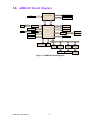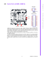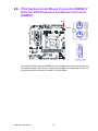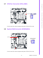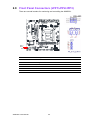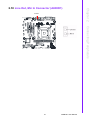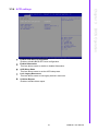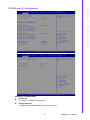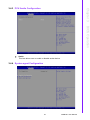
1
User Manual AIMB-501 Intel® Core™ i7/i5/i3/Celeron and Pentium® LGA1155 Micro ATX with VGA/DVI/LVDS, 10 COM, Dual Lan, 4 SATA II, 10 USB 2.0, PCIe x 16, PCIe x 1, 2 PCI Copyright The documentation and the software included with this product are copyrighted 2012 by Advantech Co., Ltd. All rights are reserved. Advantech Co., Ltd. reserves the right to make improvements in the products described in this manual at any time without notice. No part of this manual may be reproduced, copied, translated or transmitted in any form or by any means without the prior written permission of Advantech Co., Ltd. Information provided in this manual is intended to be accurate and reliable. However, Advantech Co., Ltd. assumes no responsibility for its use, nor for any infringements of the rights of third parties, which may result from its use. Acknowledgements AMI is a trademark of Phoenix Technologies Ltd. IBM and PC are trademarks of International Business Machines Corporation. Intel® Core™ i7/i5/i3, Pentium®, Celeron® is trademark of Intel Corporation WinBond is a trademark of Winbond Corporation. All other product names or trademarks are properties of their respective owners. AIMB-501 User Manual Part No. 2006050100 Edition 1 Printed in China August 2012 ii A Message to the Customer Advantech Customer Services Each and every Advantech product is built to the most exacting specifications to ensure reliable performance in the harsh and demanding conditions typical of industrial environments. Whether your new Advantech equipment is destined for the laboratory or the factory floor, you can be assured that your product will provide the reliability and ease of operation for which the name Advantech has come to be known. Your satisfaction is our primary concern. Here is a guide to Advantech’s customer services. To ensure you get the full benefit of our services, please follow the instructions below carefully. Technical Support We want you to get the maximum performance from your products. So if you run into technical difficulties, we are here to help. For the most frequently asked questions, you can easily find answers in your product documentation. These answers are normally a lot more detailed than the ones we can give over the phone. So please consult this manual first. If you still cannot find the answer, gather all the information or questions that apply to your problem, and with the product close at hand, call your dealer. Our dealers are well trained and ready to give you the support you need to get the most from your Advantech products. In fact, most problems reported are minor and are able to be easily solved over the phone. In addition, free technical support is available from Advantech engineers every business day. We are always ready to give advice on application requirements or specific information on the installation and operation of any of our products. iii AIMB-501 User Manual Declaration of Conformity FCC Class B This device complies with the requirements in part 15 of the FCC rules: Operation is subject to the following two conditions: This device may not cause harmful interference This device must accept any interference received, including interference that may cause undesired operation. This equipment has been tested and found to comply with the limits for a Class B digital device, pursuant to Part 15 of the FCC Rules. These limits are designed to provide reasonable protection against harmful interference when the equipment is operated in a commercial environment. This equipment generates, uses, and can radiate radio frequency energy and, if not installed and used in accordance with the instruction manual, may cause harmful interference to radio communications. Operation of this device in a residential area is likely to cause harmful interference in which case the user will be required to correct the interference at his/her own expense. The user is advised that any equipment changes or modifications not expressly approved by the party responsible for compliance would void the compliance to FCC regulations and therefore, the user's authority to operate the equipment. Caution! There is a danger of a new battery exploding if it is incorrectly installed. Do not attempt to recharge, force open, or heat the battery. Replace the battery only with the same or equivalent type recommended by the manufacturer. Discard used batteries according to the manufacturer's instructions. CPU Compatibility Test Item Description CPU Family sSpec. Core Power Vcore FSB Stepping L2 L3 Package Result Remark Mfg. HT cache cache Type Tech Intel® Core™ i32120 Processor SR05Y Q0 3.3 GHz 65W 5 GT/s 32nm NA NA 3MB LGA1155 PASS Intel® Core™ i52400 Processor SR00Q D2 3.1GHz 95W 5 GT/s 32nm NA NA 6MB LGA1155 PASS Intel® Core™ i72600 Processor SR00B D2 3.4 GHz 95W 5 GT/s 32nm NA NA 8MB LGA1155 PASS Intel® Celeron® Processor G540 2.50 GHz SR05J 65W 5 GT/s 32nm NA NA 2MB LGA1155 PASS Intel® Pentium® Processor G850 2.90 GHz SR05Q 65W 5 GT/s 32nm NA NA 3MB LGA1155 PASS Intel® Core™ i53550S Processor QC14 3.0GHz QS 65W 32nm NA NA 6MB LGA1155 PASS Intel® Core™ i73770 Processor 3.4 GHz QS 77W NA NA 6MB LGA1155 PASS AIMB-501 User Manual iv Memory Compatibility Test Item Description Brand Size Speed Type Vendor PN Memory 1GB DDR3 DDR3 1066 TS128MLK64V1U SEC K4B1G0846G-BCH9 PASS 2GB DDR3 DDR3 1066 TS256MLK64V1U SEC K4B1G0846G-BCH9 PASS 1GB DDR3 DDR3 1066 78.01GC3.420 ELPIDA J1108BDBG-DJ-F (128x8) PASS 2GB DDR3 DDR3 1066 78.A1GC3.421 ELPIDA J1108BDBG-DJ-F (128x8) PASS 4GB DDR3 DDR3 1066 78.B1GDJ.AF1 HYNIX H5TQ2G83BFR-H9C PASS 1GB DDR3 DDR3 1333 TS128MLK64V3U ELPIDA EDJ1108BFBG-DJ-F PASS 2GB DDR3 DDR3 1333 TS256MLK64V3U SEC K4B1G0846G-BCH9 PASS 8GB DDR3 DDR3 1333 TS1GLK64V3H MICRON IWD27 D9PBC PASS 1GB DDR3 DDR3 1333 78.01GC6.AF0 H5TQ1G83DFR-H9C PASS 1GB DDR3 DDR3 1333 78.01GC6.AF0 H5TQ1G83TFR-H9C PASS 2GB DDR3 DDR3 1333 78.A1GDE.4200C ELPIDA J2108BCSE-DJ-F PASS 2GB DDR3 DDR3 1333 78.A1GDE.AF00C Hynix H5TQ2G838FR(256x8) PASS 4GB DDR3 DDR3 1333 78.B1GDE.AF1 HYNIX H5TQ2G83BFR-H9C PASS 2GB DDR3 DDR3 1333 KVR1333D3S8N9/2G ELPIDA J2108BCSE-DJ-F(128x8) 4GB DDR3 DDR3 1333 KVR1333D3N9/4G KINGSTON D2568JENCPGD9U(512x64) PASS 2GB DDR3 DDR3 1600 D3US56081XH12AA SEC 113 HCK0 K4B2G0846C 256x8 PASS 2GB DDR3 DDR3 1600 D3US56082XH12AA SEC 113 HCK0 K4B2G0846C 256x8 PASS 4GB DDR3 DDR3 1600 TS512MLK64V6N MICRON IUM22 D9PFJ PASS Transcend Apacer Transcend Apacer Kingston DSL Transcend Result Remark PASS Ordering Information Part Number CRT DVI LVDS USB2.0 COM TPM LAN PCIe x 1 PCI slot slot AMP WES Loyalty SUSI Storage Acronis McAfee 2009 Label Access AIMB501G2KSA1E 2 (1) 1 10 10 (1) 2 1 2 Yes (3W x 2) v v v v AIMB-501LKSA1E 1 0 0 10 2 (1) 1 1 0 No v v v v AIMB501G2FKSA1E 2 (1) 1 10 10 (1) 2 1 2 Yes (3W x 2) v v v v v v AIMB501LFKSA1E 1 0 0 10 2 (1) 1 1 0 No v v v v v v *() not populated on MP version. v AIMB-501 User Manual Product Warranty (2 years) Advantech warrants to you, the original purchaser, that each of its products will be free from defects in materials and workmanship for two years from the date of purchase. This warranty does not apply to any products which have been repaired or altered by persons other than repair personnel authorized by Advantech, or which have been subject to misuse, abuse, accident or improper installation. Advantech assumes no liability under the terms of this warranty as a consequence of such events. Because of Advantech’s high quality-control standards and rigorous testing, most of our customers never need to use our repair service. If an Advantech product is defective, it will be repaired or replaced at no charge during the warranty period. For outof-warranty repairs, you will be billed according to the cost of replacement materials, service time and freight. Please consult your dealer for more details. If you think you have a defective product, follow these steps: 1. Collect all the information about the problem encountered. (For example, CPU speed, Advantech products used, other hardware and software used, etc.) Note anything abnormal and list any onscreen messages you get when the problem occurs. 2. Call your dealer and describe the problem. Please have your manual, product, and any helpful information readily available. 3. If your product is diagnosed as defective, obtain an RMA (return merchandise authorization) number from your dealer. This allows us to process your return more quickly. 4. Carefully pack the defective product, a fully-completed Repair and Replacement Order Card and a photocopy proof of purchase date (such as your sales receipt) in a shippable container. A product returned without proof of the purchase date is not eligible for warranty service. 5. Write the RMA number visibly on the outside of the package and ship it prepaid to your dealer. Initial Inspection Before you begin installing your motherboard, please make sure that the following materials have been shipped: AIMB-501 Intel LGA1155 Core i7/i5/i3 Micro ATX Motherboard SATA HDD cable x 2 I/O port bracket x 1 Startup manual x 1 Driver CD x 1 Warranty card x 1 COM port cable kit x 3 If any of these items are missing or damaged, contact your distributor or sales representative immediately. We have carefully inspected the AIMB-501 mechanically and electrically before shipment. It should be free of marks and scratches and in perfect working order upon receipt. As you unpack the AIMB-501, check it for signs of shipping damage. (For example, damaged box, scratches, dents, etc.) If it is damaged or it fails to meet the specifications, notify our service department or your local sales representative immediately. Also notify the carrier. Retain the shipping carton and packing material for inspection by the carrier. After inspection, we will make arrangements to repair or replace the unit. AIMB-501 User Manual vi Contents Chapter 1 General Information ............................1 1.1 1.2 1.3 1.9 1.10 1.11 1.12 Introduction ............................................................................................... 2 Features .................................................................................................... 2 Specifications ............................................................................................ 2 1.3.1 System .......................................................................................... 2 1.3.2 Memory ......................................................................................... 2 1.3.3 Input/Output .................................................................................. 3 1.3.4 Graphics........................................................................................ 3 1.3.5 Ethernet LAN ................................................................................ 3 1.3.6 Industrial features ......................................................................... 3 1.3.7 Mechanical and environmental specifications............................... 3 Jumpers and Connectors .......................................................................... 4 Table 1.1: Jumpers...................................................................... 4 Table 1.2: Connectors ................................................................. 4 Board layout: Jumper and Connector Locations ....................................... 5 Figure 1.1 Jumper and Connector Location ................................ 5 Figure 1.2 I/O Connectors ........................................................... 5 AIMB-501 Board Diagram ......................................................................... 6 Figure 1.3 AIMB-501 Block Diagram ........................................... 6 Safety Precautions .................................................................................... 7 Jumper Settings ........................................................................................ 7 1.8.1 How to Set Jumpers...................................................................... 7 1.8.2 CMOS Clear (CMOS1) ................................................................. 8 Table 1.3: CMOS1....................................................................... 8 1.8.3 JLVDS1: LCD Power 3.3 V/5 V/ 12 V Selector ............................. 8 Table 1.4: JLVDS1: LCD Power 3.3 V/5 V/ 12 V Selector........... 8 1.8.4 JLVDS_VBR1: Backlight control selector for LVDS1.................... 9 Table 1.5: JLVDS_VBR1: Backlight control selector for LVDS1 . 9 1.8.5 PSON1: ATX, AT Mode Selector .................................................. 9 Table 1.6: PSON1: ATX, AT Mode Selector................................ 9 1.8.6 JWDT1+JOBS1: Watchdog Timer Output and OBS Alarm Option. 9 Table 1.7: JWDT1+JOBS1: Watchdog Timer Output and OBS Alarm Option............................................................... 9 1.8.7 COM3/COM7 RS232/422/485 mode selector (JSETCOM3 & JSETCOM7)................................................................................ 10 Table 1.8: COM3 & COM7 RS 232/422/485 mode selector (JSETCOM3 & JSETCOM7) .................................... 10 1.8.8 CN1/CN2: Power setting for COM1 & COM2 ............................. 10 Table 1.9: CN1/CN2: Power setting for COM1 & COM2 ........... 10 1.8.9 JCASE1: Case Open Sensor...................................................... 11 System Memory ...................................................................................... 11 Memory Installation Procedures.............................................................. 11 Cache Memory........................................................................................ 11 Processor Installation.............................................................................. 11 2 Connecting Peripherals ....................13 2.1 2.2 Introduction ............................................................................................. 14 USB Ports (LAN1_USB12/LAN2_USB34/USB01/USB23/USB45) ......... 14 Table 2.1: LAN LED Indicator.................................................... 14 USB Power Switch .................................................................................. 15 Figure 2.1 HID-compliant Mouse Properties.............................. 15 VGA1/ DVI-D Connector (VGA1 + VGA2 + DVI1) .................................. 16 1.4 1.5 1.6 1.7 1.8 Chapter 2.3 2.4 vii AIMB-501 User Manual 2.5 2.6 Chapter 2.7 2.8 2.9 2.10 2.11 2.12 2.13 2.14 2.15 2.16 2.17 2.18 2.19 2.20 2.21 Serial Ports (COM1~COM10) ................................................................. 17 PS/2 Keyboard and Mouse Connector (KBMS1)/External PS/2 Keyboard and Mouse Connector (KBMS2) ............................................................. 18 CPU Fan Connector (CPU_FAN1) ......................................................... 19 System FAN Connector (SYSFAN1/2) ................................................... 19 Front Panel Connectors (JFP1/JFP2/JFP3) ........................................... 20 Line Out, Mic In Connector (AUDIO1) .................................................... 21 SMBUS header (SMBUS1)..................................................................... 22 Serial ATA Interface (SATA1 ~ SATA4).................................................. 22 Adjust audio volumn connector (VOL_ADJ1) ......................................... 23 PCI express x16 slot ............................................................................... 24 Front Headphone Connector (FPAUD1)................................................. 25 ATX Power Connector (EATXPWR1, ATX12V1).................................... 26 SPI Flash connector(SPI_CN1) .............................................................. 27 LCD Inverter Connector (INV1)............................................................... 28 LVDS Connector (LVDS1) ...................................................................... 29 General Purpose I/O Connector (GPIO1) ............................................... 29 LPC Connector for Debug (LPC1) .......................................................... 30 3 BIOS Operation ................................. 31 3.1 3.2 3.3 3.5 3.6 3.7 Introduction ............................................................................................. 32 BIOS Setup ............................................................................................. 32 Main BIOS Setup .................................................................................... 33 3.3.1 Advanced BIOS Features ........................................................... 34 3.3.2 PCI Configuration ....................................................................... 35 3.3.3 PCI Express Settings.................................................................. 36 3.3.4 ACPI settings .............................................................................. 37 3.3.5 Trusted Computing ..................................................................... 38 3.3.6 S5 RTC wake Settings................................................................ 38 3.3.7 SATA Configuration .................................................................... 39 3.3.8 Intel Trusted Execution Technology Configuration ..................... 39 3.3.9 USB Configuration ...................................................................... 40 3.3.10 Super IO Configuration ............................................................... 41 3.3.11 Parallel Port Configuration.......................................................... 43 3.3.12 Super IO Configuration ............................................................... 43 3.3.13 Smart Fan Configuration............................................................. 49 3.3.14 CPU PPM Configuration ............................................................. 51 Chipset Configuration Setting ................................................................. 51 3.4.1 PCH-IO Configuration................................................................ 52 3.4.2 USB Configuration ...................................................................... 56 3.4.3 PCH Azalia Configuration ........................................................... 57 3.4.4 System agent Configuration ....................................................... 57 3.4.5 NB PCIe Configuration ............................................................... 60 3.4.6 Memory Information.................................................................... 61 Boot Configuration .................................................................................. 61 Security Setting....................................................................................... 62 Save & Exit Configuration ....................................................................... 63 4 Chipset Software Installation Utility 65 4.1 4.2 4.3 Before You Begin.................................................................................... 66 Introduction ............................................................................................. 66 Windows XP/Windows 7 Driver Setup .................................................... 67 5 VGA Setup ......................................... 69 5.1 Introduction ............................................................................................. 70 3.4 Chapter Chapter AIMB-501 User Manual viii 5.2 Windows 7/XP......................................................................................... 70 6 LAN Configuration.............................71 6.1 6.2 6.3 Introduction ............................................................................................. 72 Installation ............................................................................................... 72 Windows® 7/XP Driver Setup (Realtek RTL8111E-VL).......................... 72 Appendix A Programming the Watchdog Timer..73 A.1 Programming the Watchdog Timer ......................................................... 74 A.1.1 Watchdog Timer Overview.......................................................... 74 A.1.2 Programming the Watchdog Timer ............................................. 74 Table A.1: Watchdog Timer Registers ....................................... 76 A.1.3 Example Program ....................................................................... 77 Appendix B I/O Pin Assignments..........................81 B.1 LAN&USB Connector (LAN1_USB12, LAN2_USB34)............................ 82 Table B.1: LAN&USB Connector (LAN1_USB12, LAN2_USB34) . 82 USB Connector (USB01/23/45) .............................................................. 83 Table B.2: USB Connector (USB01/23/45)................................ 83 USB/PS2 KBMS Power Setting (DUALPWR3/DUALPWR2) .................. 83 Table B.3: USB/PS2 KBMS Power Setting (DUALPWR3/ DUALPWR2) ............................................................ 83 VGA connector (VGA1/VGA2) ................................................................ 84 Table B.4: USB Connector (USB01/23/45)................................ 84 DVI Connector (DVI1) ............................................................................. 85 Table B.5: DVI Connector (DVI1)............................................... 85 COM Port Connector (COM1/COM2) ..................................................... 86 Table B.6: COM Port Connector (COM1/COM2)....................... 86 COM Port Connector (COM3456/COM78910) ....................................... 86 Table B.7: COM Port Connector (COM3456/COM78910)......... 87 KB/MS Connector (KBMS1).................................................................... 88 Table B.8: KB/MS Connector (KBMS1) ..................................... 88 KB/MS Header (KBMS2)......................................................................... 88 Table B.9: KB/MS Header (KBMS2) .......................................... 88 CPU FAN Connector (CPU FAN1).......................................................... 89 Table B.10:CPU FAN Connector (CPU FAN1) ........................... 89 System Fan Connector (SYS FAN1/SYS FAN2) .................................... 89 Table B.11:System Fan Connector (SYS FAN1/SYS FAN2)...... 89 Front Panel Connector (JFP1+JFP2)...................................................... 89 Table B.12:Front Panel Connector (JFP1+JFP2) ....................... 90 Front Panel Connector (JFP3) ................................................................ 90 Table B.13:Front Panel Connector (JFP3).................................. 90 Audio jack (AUDIO1)............................................................................... 91 Table B.14:Audio Jack (AUDIO1) ............................................... 91 SM BUS Connector (SMBUS1)............................................................... 91 Table B.15:SM BUS Connector (SMBUS1) ................................ 92 SATA Connector (SATA1/2/3/4) ............................................................. 92 Table B.16:SATA Connector (SATA1/2/3/4)............................... 92 VOLT Connector (VOLT1) ...................................................................... 92 Table B.17:VOLT Connector (VOLT1)........................................ 93 Front Audio Header (FPAUD1) ............................................................... 93 Table B.18:Front Audio Header (FPAUD1)................................. 93 ATX 24-pin Power Connector (EATXPWR1 ) ......................................... 94 Table B.19:ATX 24-pin Power Connector (EATXPWR1 )........... 94 Chapter B.2 B.3 B.4 B.5 B.6 B.7 B.8 B.9 B.10 B.11 B.12 B.13 B.14 B.15 B.16 B.17 B.18 B.19 ix AIMB-501 User Manual B.20 B.21 B.22 B.23 B.24 B.25 B.26 B.27 B.28 AIMB-501 User Manual ATX 4-pin Power Connector (ATX12V1) ................................................ 95 Table B.20:ATX 4-pin Power Connector (ATX12V1).................. 95 SPI Connector (SPI_CN1) ...................................................................... 95 Table B.21:SPI Connector (SPI_CN1)........................................ 95 Inverter Power Output (INV1) ................................................................. 96 Table B.22:Inverter Power Output (INV1)................................... 96 LVDS Connectror (LVDS1) ..................................................................... 96 Table B.23:LVDS Connectror (LVDS1) ...................................... 96 GPIO Connector (GPIO1) ....................................................................... 97 Table B.24:GPIO Connector (GPIO1) ........................................ 98 Debug Port (LPC1) ................................................................................ 98 Table B.25:Debug Port (LPC1).................................................. 98 DMA Channel Assignments .................................................................... 99 Table B.26:DMA Channel Assignments ..................................... 99 Interrupt Assignments ............................................................................. 99 Table B.27:Interrupt Assignments .............................................. 99 1st MB Memory Map............................................................................... 99 Table B.28:1st MB Memory Map ................................................ 99 x Chapter 1 1 General Information 1.1 Introduction AIMB-501 is designed with the Intel H61 for industrial applications that require both performance computing and enhanced power management capabilities. The motherboard supports Intel Core i7-3770 3.4 GHz/Core i5-3550S 3.0 GHz/Core i7-2600 3.4 GHz/Core i5-2400 3.1 GHz/Core i3-2120 3.3 GHz/ Pentium G850 2.9 GHz/Celeron G540 2.5 GHz processor up to 8 MB L3 cache and DDR3 1333/1600 up to 16 GB. It has rich I/O connectivity of 10 serial ports, 10 USB 2.0, dual GbE LAN and 4 SATA II ports. 1.2 Features Rich I/O connectivity: Dual GbE LAN via PCIe x 1 bus, 2 x PCI 32- bit/33 MHz PCI slots, 10 USB 2.0 ports, 10 serial ports, 1 PCIe x 16, and 1 PCIe x 1. Standard Micro ATX form factor with industrial feature: The AIMB-501 is a full featured Micro ATX motherboard with balanced expandability and performance. Wide selection of storage devices: SATA HDD, customers benefit from the flexibility of using the most suitable storage device for larger capacity. Optimized integrated graphic solution: With Intel® Flexible Display Interface, it supports versatile display options and 32-bit 3D graphics engine. 1.3 Specifications 1.3.1 System CPU: Intel Core i7-3770 3.4 GHz/Core i5-3550S 3.0GHz/Core i7-2600 3.4GHz/ Core i5-2400 3.1GHz /Core i3-2120 3.3GHz/ Pentium G850 2.9GHz/Celeron G540 2.5GHz processor BIOS: AMI EFI 64 Mbit SPI BIOS System chipset: Intel® H61 SATA hard disk drive interface: Four on-board SATA connectors with data transmission rate up to 300 MB 1.3.2 Memory RAM: Up to 16 GB in 2 slots 240-pin DIMM sockets. Supports dual-channel DDR3 1333/1600 MHz SDRAM. – Supports non-ECC unbuffered DIMMs and do not support any memory configuration that mixes non-ECC with ECC unbuffered DIMMs. Note! A 32-bit OS may not fully detected 16 GB of RAM when 16 GB is installed. AIMB-501 User Manual 2 1.3.4 Graphics Controller: Intel® HD Graphics Display memory: 1 GB maximum shared memory with 2GB and above system memory installed DVI: Supports DVI up to resolution 1920 x 1200 @ 60Hz refresh rate CRT1: Supports VGA up to resolution 2048 x 1536 @ 75Hz refresh rate CRT2: Up to 1920 x 1200 resolution LVDS: Supports LVDS up to resolution 1600 x 1200 1.3.5 Ethernet LAN Supports dual 10/100/1000 Mbps Ethernet port (s) via PCI Express x1 bus which provides 500 MB/s data transmission rate Controller: LAN 1: Realtek 8111E-VL; LAN 2: Realtek 8111E-VL 1.3.6 Industrial features Watchdog timer: Can generate a system reset. The watchdog timer is programmable, with each unit equal to one second or one minute (255 levels) 1.3.7 Mechanical and environmental specifications Operating temperature: 0 ~ 60° C (32 ~ 140° F, depending on CPU) Storage temperature: -40 ~ 85° C (-40 ~ 185° F) Humidity: 5 ~ 95% non-condensing Power supply voltage: +3.3 V, +5 V, +12 V, -12 V, 5 Vsb Power consumption: -Intel LGA1155 Core i7-3770 3.4 GHz, 8MB L3 cache, 2pcs 8GB DDR3 1333 MHz, +5V @ 1.92A, +3.3V @ 1.03A, +12V @ 5.53A, 5Vsb @ 0.28A, -12V@ 0.11A Measure the maximum current value which system under maximum load (CPU: Top speed, RAM: Full loading) Board size: 244 mm x 244 mm (9.6" x 9.6") Board weight: 0.5 kg 3 AIMB-501 User Manual General Information PCIe slot: 1 PCIe x16 expansion slot and 1 PCIe x1 expansion slot. PCIe Bus: 2 PCI slots, 32-bit/33 MHz PCI 2.2 compliant Parallel port: Configured to LPT1 or disabled. LPT1 supports EPP/SPP/ECP. Serial port: Ten serial ports, two RS-232/422/485 with hardware auto-flow control and eight RS-232. Keyboard and PS/2 mouse connector: Two 6-pin mini-DIN connectors are located on the mounting bracket for easy connection to PS/2 keyboard and mouse. USB port: Supports up to 10 USB 2.0 ports with transmission rates up to 480 Mbps. GPIO: AIMB-501 supports 8-bit GPIO from super I/O for general purpose control application. Chapter 1 1.3.3 Input/Output 1.4 Jumpers and Connectors Connectors on the AIMB-501 motherboard link it to devices such as hard disk drives and a keyboard. In addition, the board has a number of jumpers used to configure your system for your application. The tables below list the function of each of the board jumpers and connectors. Later sections in this chapter give instructions on setting jumpers. Chapter 2 gives instructions for connecting external devices to your motherboard. Table 1.1: Jumpers Label Function CMOS1 Clear CMOS (Default 1-2) JLVDS1 LVDS panel power setting JLVDS_VBR1 Panel brightness control (Linear or PWM) PSON1 AT mode (1-2); ATX mode (2-3) JWDT1+JOBS1 Watchdog reset + OBS alarm JSETCOM3/ JSETCOM7 COM3 & COM7 RS-232/422/485 jumper setting CN1/CN2 5V (3-4); 12V (5-6) JCASE1 Case open sensor Table 1.2: Connectors Label Function VGA1/VGA2 VGA1/VGA2 connector DVI1 DVI connector INV1 Inverter power output LVDS1 LVDS connector LANLED1 LAN LED LAN1_USB12; LAN2_USB34 LAN & USB & external connector FPAUD1 Front audio header VOL_ADJ1 Adjust audio volume AUDIO1 Line out /Mic in connector SATA1/2/3/4 SATA1/2/3/4 on board connector USB01/23/45 USB on board connector SPI_CN1 SPI connector LPC1 LPC connector for debug LPT1 Print port COM1/COM2 Serial port 1/2 on board connector COM3456/COM78910 Serial port 3/4/5/6/7/8/9/10 on board connector KBMS2 KB, MS header CPU FAN1 CPU fan connector SYS FAN1/SYS FAN2 FAN2System fan connector GPIO1 GPIO connector VOLT1 VOLT connector JFP3 Front panel connector JWDT1+JOBS1 Watchdog reset + OBS alarm SMBUS1 SMBUS header AIMB-501 User Manual 4 JFP1+JFP2 Power and reset button connector + HDD LED/SNMP SMbus/ speaker connector 1.5 Board layout: Jumper and Connector Locations LPT1 KBMS1 VGA1 KBMS2 DUALPWR3 INV1 LVDS1 JLVDS2 JLVDS1 ATX12V1 JLVDS_VBR1 PCIEX1_1 LANLED1 SYSFAN1 USB45 DVI1 CPU_FAN1 PSON1 USB23 SMBUS1 COM2 CN2 CN1 COM1 USB01 DUALPWR2 DIMM_A1 DIMM_B1 VOLT1 SPI_CN1 SATA4 JFP1+JFP2 JFP3 SATA3 SATA1 COM78910 COM3456 SATA2 JWDT1+JOBS1 JSETCOM3 JSETCOM7 GPIO1 SYSFAN2 EATXPWR1 Figure 1.1 Jumper and Connector Location Figure 1.2 I/O Connectors 5 AIMB-501 User Manual General Information LAN2_USB34 VGA2 VOL_ADJ1 PCI1 FPAUD1 PCI2 PCIEx16_1AUDIO1 LAN1_USB12 Chapter 1 Table 1.2: Connectors 1.6 AIMB-501 Board Diagram Dual Channel LVDS Chrontel 7308B DDR3 1333/1600 MHz Channel B DDR3 1333/1600 MHz Interface Flex Display Direct Media LVDS Channel A Intel Core i7/i5/i3 PCIEx16 Interface PCIex16 SDVO PCIex1 RTL 8111E-VL : LAN PCIex1 RTL 8111E-VL:LAN2 1 PCIex1 PCIex1 connector 24 bit/Channel CRT 1 CRT2 CRT Chrontel 7317 H61 SDVO PCI1 connector IT8892F PCIex1 USB 2.0 4 SATA2 Ports 300MB/s Audio Codec Realtek ALC892 SPI 10 USB Ports LPC BUS BIOS TPM (Optional) Fintek 81216AD Fintek 81216AD Super I/O Nuvuton 6776F 4 RS-232 (1 w/RS-422/485) 4 RS-232 (1 w/RS-422/485) 2 x RS-232, PS/2, Parallel, GPIO,WDT Figure 1.3 AIMB-501 Block Diagram AIMB-501 User Manual 32 bit/33 MHz PCI Bus PCI2 connector Audio DVI Intel HD DVI 6 Warning! Always completely disconnect the power cord from chassis whenever you work with the hardware. Do not make connections while the power is on. Sensitive electronic components can be damaged by sudden power surges. Only experienced electronics personnel should open the PC chassis. Caution! The computer is provided with a battery-powered real-time clock circuit. There is a danger of explosion if battery is incorrectly replaced. Replace only with same or equivalent type recommended by the manufacturer. Discard used batteries according to manufacturer's instructions. Caution! There is a danger of a new battery exploding if it is incorrectly installed. Do not attempt to recharge, force open, or heat the battery. Replace the battery only with the same or equivalent type recommended by the manufacturer. Discard used batteries according to the manufacturer’s instructions. 1.8 Jumper Settings This section provides instructions on how to configure your motherboard by setting the jumpers. It also includes the motherboards's default settings and your options for each jumper. 1.8.1 How to Set Jumpers You can configure your motherboard to match the needs of your application by setting the jumpers. A jumper is a metal bridge that closes an electrical circuit. It consists of two metal pins and a small metal clip (often protected by a plastic cover) that slides over the pins to connect them. To “close” (or turn ON) a jumper, you connect the pins with the clip. To “open” (or turn OFF) a jumper, you remove the clip. Sometimes a jumper consists of a set of three pins, labeled 1, 2, and 3. In this case you connect either pins 1 and 2, or 2 and 3. A pair of needle-nose pliers may be useful when setting jumpers. 7 AIMB-501 User Manual General Information Caution! Always ground yourself to remove any static charge before touching the motherboard. Modern electronic devices are very sensitive to electrostatic discharges. As a safety precaution, use a grounding wrist strap at all times. Place all electronic components on a static-dissipative surface or in a static-shielded bag when they are not in the chassis. Chapter 1 1.7 Safety Precautions 1.8.2 CMOS Clear (CMOS1) The AIMB-501 motherboard contains a jumper that can erase CMOS data and reset the system BIOS information. Normally this jumper should be set with pins 1-2 closed. If you want to reset the CMOS data, set CMOS1 to 2-3 closed for just a few seconds, and then move the jumper back to 1-2 closed. This procedure will reset the CMOS to its default setting. Table 1.3: CMOS1 Function Jumper Setting *Keep CMOS data 1-2 closed Clear CMOS data 2-3 closed * Default 1.8.3 JLVDS1: LCD Power 3.3 V/5 V/ 12 V Selector Table 1.4: JLVDS1: LCD Power 3.3 V/5 V/ 12 V Selector Closed Pins Result JLVDS1 2-3 Jumper for 5V LVDS panel 1-2 Jumper for 3.3V LVDS panel* 2-2 Jumper for 12V LVDS panel *Default AIMB-501 User Manual 8 Table 1.5: JLVDS_VBR1: Backlight control selector for LVDS1 Closed Pins Result 1-2* Linear brightness control 2-3 PWM brightness control *Default General Information 1.8.5 PSON1: ATX, AT Mode Selector Table 1.6: PSON1: ATX, AT Mode Selector Closed Pins Result 1-2 AT Mode 2-3* ATX Mode *Default 1.8.6 JWDT1+JOBS1: Watchdog Timer Output and OBS Alarm Option Table 1.7: JWDT1+JOBS1: Watchdog Timer Output and OBS Alarm Option Closed Pins Result 1-2 NC *2-3 Reset *4-5 Enable OBS function (4-5 open: disable OBS function) *: Default 9 Chapter 1 1.8.4 JLVDS_VBR1: Backlight control selector for LVDS1 AIMB-501 User Manual 1.8.7 COM3/COM7 RS232/422/485 mode selector (JSETCOM3 & JSETCOM7) Users can use JSETCOM3 & JSETCOM7 to select among RS232/422/485 mode for COM3 & COM7. The default setting is RS232. Table 1.8: COM3 & COM7 RS 232/422/485 mode selector (JSETCOM3 & JSETCOM7) Function Jumper Setting *RS232 (5-6) + (7-9) + (8-10) + (13-15) + (14-16) closed RS422 (3-4) + (9-11) + (10-12) + (15-17) + (16-18) closed RS-485 (1-2) + (9-11) + (10-12) + (15-17) + (16-18) closed *: Default 1.8.8 CN1/CN2: Power setting for COM1 & COM2 Table 1.9: CN1/CN2: Power setting for COM1 & COM2 Setting Function 1-2 No power 3-4 with 5V 5-6 with 12V AIMB-501 User Manual 10 The AIMB-501 motherboard contains a jumper that provides a chassis open sensor. The buzzer on the motherboard beeps when the case is opened. 1.9 System Memory AIMB-501 has two 240-pin memory sockets for 1333/1600 MHz memory modules with maximum capacity of 16GB (Maximum 8GB for each DIMM). AIMB-501 supports only non-ECC DDR3 memory modules. To install DIMMs, first make sure the two handles of the DIMM socket are in the “open” position, i.e., the handles lean outward. Slowly slide the DIMM module along the plastic guides on both ends of the socket. Then firmly but gently (avoid pushing down too hard) press the DIMM module well down into the socket, until you hear a click when the two handles have automatically locked the memory module into the correct position of the DIMM socket. To remove the memory module, just push both handles outward, and the memory module will be ejected by the mechanism. 1.11 Cache Memory The AIMB-501 supports a CPU with one of the following built-in full speed L3 caches: 8 MB for Intel Core i7-3770 6 MB for Intel Core i5-3550S 3 MB for Intel Core i3-3220 8 MB for Intel Core i7-2600 6 MB for Intel Core i5-2400 3 MB for Intel Core i3-2120 3 MB for Intel Pentium G850 2 MB for Intel Celeron G540 The built-in second-level cache in the processor yields much higher performance than conventional external cache memories. 1.12 Processor Installation The AIMB-501 is designed for LGA1155, Intel Core i7/Core i5/Core i3/Pentium/Celeron processor. 11 AIMB-501 User Manual General Information 1.10 Memory Installation Procedures Chapter 1 1.8.9 JCASE1: Case Open Sensor AIMB-501 User Manual 12 Chapter 2 Connecting Peripherals 2 2.1 Introduction You can access most of the connectors from the top of the board as it is being installed in the chassis. If you have a number of cards installed or have a packed chassis, you may need to partially remove the card to make all the connections. 2.2 USB Ports (LAN1_USB12/LAN2_USB34/USB01/ USB23/USB45) The AIMB-501 provides up to 10 USB ports. The USB interface complies with USB Specification Rev 2.0 supporting transmission rates up to 480 Mbps. The USB interface can be disabled in the system BIOS setup. The AIMB-501 is equipped with two high-performance 1000 Mbps Ethernet LAN adapters, both of which are supported by all major network operating systems. The RJ-45 jacks on the rear panel provides convenient LAN connection. LAN2_USB34 LAN1_USB12 USB45 USB23 USB01 Table 2.1: LAN LED Indicator LAN Mode LAN1 indicator LAN2 indicator AIMB-501 User Manual LAN Indicator LED1 (Right) off for mal-link; Link (On) / Active (Flash) LED2 (Left) 100 Mbps (On) / 10 Mbps (Off) LED2 (Left) 1000 Mbps (On) LED1 (Right) off for mal-link; Link (On) / Active (Flash) LED2 (Left) 100 Mbps (On) / 10 Mbps (Off) LED2 (Left) 1000 Mbps (On) 14 AIMB-501 allows users to set USB power between +5VSB and +5V. When the jumper is set as 2-3, do not tick "Allow this device to bring the computer out of standby" under device manager (as below figure 2.1) if users do not request to have the board wake up from S3 via USB device keyboard or mouse. Chapter 2 2.3 USB Power Switch DUALPWR3 Connecting Peripherals DUALPWR2 Figure 2.1 HID-compliant Mouse Properties DUALPWR3/DUALPWR2 USB/PS2 KBMS Power setting Setting Function 1-2 USB/PS2 KBMS power from MOS 2-3 USB/PS2 KBMS power from +5V 15 AIMB-501 User Manual DUALPWR2- Jumper for on board USB DUALPWR3- Jumper for rear side USB & PS/2 KBMS Note! When USB power is switched to +5V, it can't be connected with power KVM. 2.4 VGA1/ DVI-D Connector (VGA1 + VGA2 + DVI1) VGA2 VGA1 VGA1 DVI1 VGA2 AIMB-501 includes VGA and DVI interfaces that can drive conventional VGA and DVI displays. VGA is a standard 15-pin D-SUB connector commonly used for VGA. Pin assignments for VGA and DVI connectors are detailed in Appendix B. AIMB-501 User Manual 16 Chapter 2 2.5 Serial Ports (COM1~COM10) COM1 COM3/4/5/6 COM7/8/9/10 AIMB-501 supports ten serial ports. COM1. COM2. COM4-6. COM8-10 supports RS232. COM3 & COM7 supports RS-232/422/485 (supports RS-485 auto flow control). JSETCOM3 & JSETCOM7 is used to select the RS-232/422/485 mode for COM3 & COM7. COM1 & COM2 is with selectable 5V/12V power.. These ports can connect to serial devices, such as a mouse or a printer, or to a communications network. The IRQ and address ranges for both ports are fixed. However, if you want to disable the port or change these parameters later, you can do this in the system BIOS setup. Different devices implement the RS-232 standards in different ways. If you have problems with a serial device, be sure to check the pin assignments for the connector. 17 AIMB-501 User Manual Connecting Peripherals COM2 2.6 PS/2 Keyboard and Mouse Connector (KBMS1)/ External PS/2 Keyboard and Mouse Connector (KBMS2) KBMS1 KBMS2 Two 6-pin mini-DIN connectors (KBMS1) on the motherboard provide connection to a PS/2 keyboard and a PS/2 mouse, respectively. KBMS2 is for supporting the 2nd PS/ 2 keyboard and PS/2 mouse by a cable P/N 1700018699. AIMB-501 User Manual 18 Chapter 2 2.7 CPU Fan Connector (CPU_FAN1) If a fan is used, this connector supports cooling fans of 500 mA (6 W) or less. 2.8 System FAN Connector (SYSFAN1/2) SYSFAN1 SYSFAN2 If a fan is used, this connector supports cooling fans of 500 mA (6 W) or less. 19 AIMB-501 User Manual Connecting Peripherals CPU_FAN1 2.9 Front Panel Connectors (JFP1/JFP2/JFP3) There are several headers for monitoring and controlling the AIMB-501. JFP1+ JFP2 JFP3 JFP3 Front panel connector Pin Pin Name 1 SIO_SUSLED 2 NC 3 GND 4 #KEYLOCK 5 GND AIMB-501 User Manual 20 AUDIO1 Chapter 2 2.10 Line Out, Mic In Connector (AUDIO1) Connecting Peripherals 21 AIMB-501 User Manual 2.11 SMBUS header (SMBUS1) AIMB-501 provides SMBUS connector for customer connection to SMBUS protocol embedded device. It can be configured to I2C by customer's request. SMBUS1 2.12 Serial ATA Interface (SATA1 ~ SATA4) SATA4 SATA3 SATA1 SATA2 AIMB-501 features a high performance Serial ATA interface (up to 300 MB/s) which eases hard drive cabling with thin, space-saving cables. AIMB-501 User Manual 22 VOL_ADJ1 Adjust audio volume Pin Pin Name 1 AMP_L_OUT_C 2 AMP_L_OUT 3 GND 4 AMP_R_OUT 5 AMP_R_OUT_C VOL_ADJ1 connects to the alarm board on the chassis. These alarm boards give warnings if a power supply or fan fails, or if the chassis overheats. 23 AIMB-501 User Manual Connecting Peripherals VOL_ADJ1 Chapter 2 2.13 Adjust audio volumn connector (VOL_ADJ1) 2.14 PCI express x16 slot PCIEx16_1 AIMB-501 provides a PCIe x16 slot for users to install add-on cards when their applications require higher graphic performance than the CPU embedded graphics controller can provide. AIMB-501 User Manual 24 This connector is for a chassis-mounted front panel audio I/O module that supports either HD Audio or legacy AC’97 (optional) audio standard. Connect this connector with the front panel audio I/O module cable. FPAUD1 Chapter 2 2.15 Front Headphone Connector (FPAUD1) Connecting Peripherals FPAUD1 Front audio header Pin Pin Name 1 MIC2_L 2 GND 3 MIC2_R 4 F_AUDIO_DET# 5 LIN2_R 6 MIC2_JD 7 SENSE_B 8 NC 9 LIN2_L 10 LIN2_JD Note! For motherboards with the optional HD Audio feature, we recommend that you connect a high-definition front panel audio module to this connector to take advantage of the motherboard’s high definition audio capability. 25 AIMB-501 User Manual 2.16 ATX Power Connector (EATXPWR1, ATX12V1) This connector is for an ATX Micro-Fit power supply. The plugs from the power supply are designed to fit these connectors in only one direction. Determine the proper orientation and push down firmly until the connectors mate completely. ATX12V1 EATXPWR1 Note! 1. 2. AIMB-501 User Manual Please connect the ATX12V1 connector with the PSU ATX 12V 4pin connector. For a fully configured system, we recommend that you use a power supply unit (PSU) that complies with ATX 12 V Specification 2.0 (or later version) and provides a minimum power of 180 W. 26 The SPI flash card pin header may be used to flash the BIOS if the AIMB-501 cannot power on. Connecting Peripherals SPI_CN1 SPI_CN1 Chapter 2 2.17 SPI Flash connector(SPI_CN1) SPI connector Pin Pin Name 1 SPI_POWER 2 GND 3 SPI_CS# 4 SPI_CLK 5 SPI_MISO 6 SPI_MOSI 7 NC 8 SPI_HOLD# 27 AIMB-501 User Manual 2.18 LCD Inverter Connector (INV1) INV1 INVI Inverter Power Output Pin Pin Name 1 +12V 2 GND 3 ENABKL 4 VBR 5 +5V AIMB-501 User Manual 28 Chapter 2 2.19 LVDS Connector (LVDS1) LVDS1 GPIO1 GPIO1 GPIO connector Pin Pin Name 1 SIO_SPIO0 2 SIO_SPIO1 29 AIMB-501 User Manual Connecting Peripherals 2.20 General Purpose I/O Connector (GPIO1) 3 SIO_SPIO2 4 SIO_SPIO3 5 SIO_SPIO4 6 SIO_SPIO5 7 SIO_SPIO6 8 SIO_SPIO7 9 VCC_GPIO 10 GND 2.21 LPC Connector for Debug (LPC1) LPC1 AIMB-501 User Manual 30 Chapter 3 BIOS Operation 3 3.1 Introduction AMI BIOS has been integrated into many motherboards, and has been very popular for over a decade. People sometimes refer to the AMI BIOS setup menu as BIOS, BIOS setup or CMOS setup. With the AMI BIOS Setup program, you can modify BIOS settings to control the special features of your computer. The Setup program uses a number of menus for making changes. This chapter describes the basic navigation of the AIMB-501 setup screens. 3.2 BIOS Setup The AIMB-501 Series system has AMI BIOS built in, with a CMOS SETUP utility that allows users to configure required settings or to activate certain system features. The CMOS SETUP saves the configuration in the CMOS RAM of the motherboard. When the power is turned off, the battery on the board supplies the necessary power to preserve the CMOS RAM. When the power is turned on, press the <Del> button during the BIOS POST (PowerOn Self Test) to access the CMOS SETUP screen. Control Keys < ↑ >< ↓ >< ← >< → > Move to select item <Enter> Select Item <Esc> Main Menu - Quit and not save changes into CMOS Sub Menu - Exit current page and return to Main Menu <Page Up/+> Increase the numeric value or make changes <Page Down/-> Decrease the numeric value or make changes <F1> General help, for Setup Sub Menu <F2> Item Help <F5> Load Previous Values <F7> Load Setup Defaults <F10> Save all CMOS changes AIMB-501 User Manual 32 Press <Del> to enter AMI BIOS CMOS Setup Utility, the Main Menu will appear on the screen. Use arrow keys to select among the items and press <Enter> to accept or enter the sub-menu. Chapter 3 3.3 Main BIOS Setup BIOS Operation The Main BIOS setup screen has two main frames. The left frame displays all the options that can be configured. Grayed-out options cannot be configured; options in blue can. The right frame displays the key legend. Above the key legend is an area reserved for a text message. When an option is selected in the left frame, it is highlighted in white. Often a text message will accompany it. System time / System date Use this option to change the system time and date. Highlight System Time or System Date using the <Arrow> keys. Enter new values through the keyboard. Press the <Tab> key or the <Arrow> keys to move between fields. The date must be entered in MM/DD/YY format. The time must be entered in HH:MM:SS format. 33 AIMB-501 User Manual 3.3.1 Advanced BIOS Features Select the Advanced tab from the AIMB-501 setup screen to enter the Advanced BIOS Setup screen. You can select any of the items in the left frame of the screen, such as CPU Configuration, to go to the sub menu for that item. You can display an Advanced BIOS Setup option by highlighting it using the <Arrow> keys. All Advanced BIOS Setup options are described in this section. The Advanced BIOS Setup screen is shown below. The sub menus are described on the following pages. AIMB-501 User Manual 34 Chapter 3 3.3.2 PCI Configuration BIOS Operation Above 4G Decoding To disabled or enabled “Above 4G Decoding”. When select enabled, it could enhance the compatibility for 64bit PCI device. PCI Latency Timer Use this to adjust the PCI Latency Timer. This option sets the latency of all PCI devices on the PCI bus. The Optimal and Fail-Safe default setting is 32. VGA Palette Snoop Set this value to allow the system to modify the VGA Palette Snoop settings. The Optimal and Fail-Safe default setting is "Disabled". 35 AIMB-501 User Manual 3.3.3 PCI Express Settings Link Training Retry To adjust the retry times when PCIE Link failure Link Training Timeout To set up timeout for link training AIMB-501 User Manual 36 Chapter 3 3.3.4 ACPI settings BIOS Operation Enable ACPI Auto Configuration Enable or disable BIOS ACPI auto configuration. Enable Hibernation This item allows users to enable or disable Hibernation. ACPI Sleep State This item allows users to set the ACPI sleep state Lock Legacy Resources This item allows users to lock legacy devices’ resources. S3 Video Repost Enable or disable video repost. 37 AIMB-501 User Manual 3.3.5 Trusted Computing Security Device Support Enable or disable BIOS support for security device. 3.3.6 S5 RTC wake Settings Wake system with fixed time Enable or disable system wake on alarm event. AIMB-501 User Manual 38 Chapter 3 3.3.7 SATA Configuration BIOS Operation SATA Controllers To enable or disable SATA controller. SATA Mode Selection This can be configured as IDE or AHCI mode. 3.3.8 Intel Trusted Execution Technology Configuration 39 AIMB-501 User Manual Secure Mode Extension (SMX) This item allows users to enable or disable SMX. Intel TXT Configuration This item allow users to enable or disable Intel Trusted Execution Technology. 3.3.9 USB Configuration Legacy USB Support Enables support for legacy USB. Auto option disables legacy support if no USB devices are connected. EHCI Hand-off This is just a workaround item under OS without EHCI hand-off support. USB hardware delays and time-outs To set up parameter for detect USB device. Mass Storage Devices Shows USB mass storage device information. AIMB-501 User Manual 40 Chapter 3 3.3.10 Super IO Configuration BIOS Operation Serial Port 1 Configuration Serial Port To “enable” or “disable” Serial Port 1. Change Settings To select the IO address/IRQ setting for serial port 1. 41 AIMB-501 User Manual Serial Port 2 Configuration Serial Port To “enable” or “disable” Serial Port 2. Change Settings To select the IO address/IRQ setting for serial port 2. AIMB-501 User Manual 42 Chapter 3 3.3.11 Parallel Port Configuration BIOS Operation Parallel Port To enable or disable Parallel Port. 3.3.12 Super IO Configuration Serial Port 3 Configuration Serial Port 43 AIMB-501 User Manual To “enable” or “disable” Serial Port 3. Change Settings To select the IO address/IRQ setting for serial port 3. Auto flow control When the COM is to set as RS-485, it supports auto flow control function. Serial Port 4 Configuration Serial Port To “enable” or “disable” Serial Port 4. Change Settings To select the IO address/IRQ setting for serial port 4. AIMB-501 User Manual 44 Chapter 3 BIOS Operation Serial Port 5 Configuration Serial Port To ‚”enable” or “disable” Serial Port 5. Change Settings To select the IO address/IRQ setting for serial port 5. 45 AIMB-501 User Manual Serial Port 6 Configuration Serial Port To “enable” or “disable” Serial Port 6. Change Settings To select the IO address/IRQ setting for serial port 6. Serial Port 7 Configuration Serial Port To “enable” or “disable” Serial Port 7. Change Settings To select the IO address/IRQ setting for serial port 7. Auto flow control When the COM is to set as RS-485, it supports auto flow control function. AIMB-501 User Manual 46 Chapter 3 BIOS Operation Serial Port 8 Configuration Serial Port To “enable” or “disable” Serial Port 8. Change Settings To select the IO address/IRQ setting for serial port 8. Serial Port 9 Configuration Serial Port 47 AIMB-501 User Manual To “enable” or “disable” Serial Port 9. Change Settings To select the IO address/IRQ setting for serial port 9. Serial Port 10 Configuration Serial Port To “enable” or “disable” Serial Port 10. Change Settings To select the IO address/IRQ setting for serial port 10. AIMB-501 User Manual 48 Chapter 3 3.3.13 Smart Fan Configuration BIOS Operation CPU Smart Fan To enable or disable CPU smart fan. System Smart Fan To enable or disable System Smart Fan. 49 AIMB-501 User Manual CPU Warning Temperature Use this to set the CPU warning temperature threshold. When the system CPU reaches the warning temperature, the buzzer will beep. ACPI Shutdown Temperature This screen allows users to set the CPU temperature at which the system will automatically shut down to prevent the CPU from overheating damage. AIMB-501 User Manual 50 Chapter 3 3.3.14 CPU PPM Configuration BIOS Operation EIST CPU runs at its default speed if disabled; CPU speed is controlled by the operating system if enabled. CPU C3/C6/C7 Report This item allows users to enable or disable CPU C-state support. ACPI T state This item allows users to enable or disable ACPI T state function. 3.4 Chipset Configuration Setting Select the chipset tab from the BIOS setup screen to enter the Chipset Setup screen. Users can select any item in the left frame of the screen, such as PCI express Configuration, to go to the sub menu for that item. Users can display a Chipset Setup option by highlighting it using the <Arrow> keys. All Chipset Setup options are described in this section. The Chipset Setup screens are shown below. The sub menus are described on the following pages. 51 AIMB-501 User Manual 3.4.1 PCH-IO Configuration PCI Express Configuration Detail of PCI Express items. USB Configuration Details of USB items. PCH Azalia Configuration Details of PCH azalia items. AIMB-501 User Manual 52 3.4.1.1 PCI Express Configuration PCI Express Clock Gating Enable or disable PCI express clock gating. Subtractive Decode Enable or disable Subtractive decode. 53 AIMB-501 User Manual BIOS Operation LAN controller Enables or disables the LAN1/2 controller. LAN option-ROM Enables or disables the LAN1/2 option-ROM. PCIE Wake Enables or disables PCIE device wake up from sleep state. High Precision Timer Enables or disables the high precision timer. SLP_S4 Assertion Width This item allows users to set a delay of sorts. Restore AC Power Loss This item allows users to select off, on and last state. Chapter 3 3.4.1.2 PCI Express Root Port 1/2/3 AIMB-501 User Manual 54 Chapter 3 BIOS Operation This pages allow users to adjust parameter for PCI express root port 1&2&3. ASPM Support Allow user to set the ASPM Level. Force L0s - Force all links to L0s State. AUTO - BIOS auto configure. DISABLE - Disables ASPM. URR Enable or disable PCI Express Unsupported Request Reporting. FER Enable or disable PCI Express Device Fatal Error Reporting. NFER Enable or disable PCI Express Device Non-Fatal Error Reporting. CER Enable or disable PCI Express Device Correctable Error Reporting. CTO Enable or disable PCI Express Completion Timer TO. SEFE Enable or disable Root PCI Express System Error on Fatal Error. SENFE Enable or disable Root PCI Express System Error on Non-Fatal Error. SECE Enable or disable Root PCI Express System Error on Correctable Error. PME SCI Enable or disable PCI Express PME SCI. Hot Plug Enable or disable PCI Express Hot Plug. PCIe Speed Select PCI Express port speed. Extra Bus Reserved 55 AIMB-501 User Manual Extra Bus Reserved for bridges behind this Root Bridge. Reserved Memory Reserved Memory Range for this Root Bridge. Prefetchable Memory Prefetchable Memory Range for this Root Bridge. Reserved I/O Reserved I/O (4K/8K/12K/16K/20K) Range for this Root Bridge 3.4.2 USB Configuration EHCI 1/2 Enables or disables the EHCI controller. USB Ports pre-port Disable Control This item allows users to enable or disable each USB port individually. AIMB-501 User Manual 56 Chapter 3 3.4.3 PCH Azalia Configuration BIOS Operation Azalia This item allows user to enable or disable azalea device. 3.4.4 System agent Configuration 57 AIMB-501 User Manual Primary Display This item allows users to select which graphics controller to use as the primary boot device. Internal Graphics This item allows users to enable or disable IGD. GTT Size This item allows users to select GTT size. Aperture Size This item allows users to select aperture size. DVMT Pre-Allocated This item allows users to select DVMT pre-allocated memory size. DVMT Total Gfx Mem This item allows users to select DVMT total memory size. LCD Control This item allows users to setup Display Control configuration. AIMB-501 User Manual 58 Chapter 3 3.4.4.1 LCD Control configuration BIOS Operation Primary IGFX Boot Display This items allow users to select the video device which will be activated during post. The available options are VBIOS Default, VGA1, LVDS/VGA2, DVI. SDVO-LFP Panel Type: 1024 x 768 18-bit 1024 x 768 24-bit 1280 x 1024 48-bit 1366 x 768 24-bit 59 AIMB-501 User Manual 3.4.5 NB PCIe Configuration PEG0 - Gen x Select PEG0 speed. – PEG0 ASPM=> Enable/Disable PEG0 ASPM function. (ASPM: Active State Power Management) Enable PEG This item allows users to enable or disable PEG always. Detect Non-Compliance Device This item allows users to enable or disable Detect Non-Compliance Device function. AIMB-501 User Manual 60 Chapter 3 3.4.6 Memory Information BIOS Operation Memory Frequency Limiter Select memory frequency limiter for auto, 1067, 1333, 1600. 3.5 Boot Configuration 61 AIMB-501 User Manual Setup Prompt Timeout This item allows you to change number of seconds to wait for setup activation key. Bootup NumLock State Select the Power-on state for Numlock. Quiet Boot If this option is set to Disabled, the BIOS display normal POST messages. If Enabled, an OEM Logo is shown instead of POST messages. GateA20 Active This item allows you to select upon request or always. Option ROM Messages Sets display mode for option ROM. INT19 Trap Response This item allows option ROMs to trap interrupt 19. Boot Option PrioritiesNT19 Trap Response Set the system boot order. 3.6 Security Setting Select Security Setup from the AIMB-501 Setup main BIOS setup menu. All Security Setup options, such as password protection and virus protection are described in this section. To access the sub menu for the following items, select the item and press<Enter>: Change Administrator / User Password. Administrator Password Select this option and press <ENTER> to access the sub menu, and then type in the password. Set the Administrator password. User Password AIMB-501 User Manual 62 3.7 Save & Exit Configuration Chapter 3 Select this option and press <ENTER> to access the sub menu, and then type in the password. Set the User Password. BIOS Operation 1. 2. 1. 2. Save Changes and Exit When users have completed system configuration, select this option to save changes, exit BIOS setup menu and reboot the computer to take effect all system configuration parameters. Select Exit Saving Changes from the Exit menu and press <Enter>. The following message appears: Save Configuration Changes and Exit Now? [Ok] [Cancel] Select Ok or cancel. Discard Changes and Exit Select this option to quit Setup without making any permanent changes to the system configuration. Select Exit Discarding Changes from the Exit menu and press <Enter>. The following message appears: Discard Changes and Exit Setup Now? [Ok] [Cancel] Select Ok to discard changes and exit. Discard Changes Select Discard Changes from the Exit menu and press <Enter>. Restore Default The BIOS automatically configures all setup items to optimal settings when users select this option. Defaults are designed for maximum system performance, but may not work best for all computer applications. In particular, do not use the Defaults if the user's computer is experiencing system configuration problems. Select Restore Defaults from the Exit menu and press <Enter>. Save as User Default Save the all current settings as a user default. Restore User Default 63 AIMB-501 User Manual Restore all settings to user default values. Boot Override Shows the boot device types on the system. AIMB-501 User Manual 64 Chapter 4 Chipset Software Installation Utility 4 4.1 Before You Begin To facilitate the installation of the enhanced display drivers and utility software, read the instructions in this chapter carefully. The drivers for AIMB-501 are located on the software installation CD. The driver in the folder of the driver CD will guide and link you to the utilities and drivers under a Windows system. Updates are provided via Service Packs from Microsoft*. Note! The files on the software installation CD are compressed. Do not attempt to install the drivers by copying the files manually. You must use the supplied SETUP program to install the drivers. Before you begin, it is important to note that most display drivers need to have the relevant software application already installed in the system prior to installing the enhanced display drivers. In addition, many of the installation procedures assume that you are familiar with both the relevant software applications and operating system commands. Review the relevant operating system commands and the pertinent sections of your application software’s user manual before performing the installation. 4.2 Introduction The Intel Chipset Software Installation (CSI) utility installs the Windows INF files that outline to the operating system how the chipset components will be configured. This is needed for the proper functioning of the following features: Core PCI PnP services IDE Ultra ATA 100/66/33 and Serial ATA interface support USB 1.1/2.0 support (USB 2.0 driver needs to be installed separately for Win98) Identification of Intel chipset components in the Device Manager Note! This utility is used for the following versions of Windows, and it has to be installed before installing all the other drivers: Windows 7 (32-bit) Windows 7 (64-bit) Windows XP professional edition (32-bit) Windows XP professional edition (64-bit) AIMB-501 User Manual 66 1. Insert the driver CD into your system's CD-ROM drive. You can see the driver folder items. Navigate to the "Intel chip" folder and click "Setup.exe" to complete the installation of the driver. Chapter 4 4.3 Windows XP/Windows 7 Driver Setup Chipset Software Installation Utility 67 AIMB-501 User Manual AIMB-501 User Manual 68 Chapter 5 VGA Setup 5 5.1 Introduction The Intel Core i7-3770, Core i5-3550S, Core i3-3220, Core i7-2600, Core i5-2400, Core i3-2120, Pentium G850, Celeron G540 CPUs with dual cores are embedded with an integrated graphics controller. You need to install the VGA driver to enable this function. Optimized integrated graphic solution: With Intel Graphics Flexible, versatile display options and 32-bit 3D graphics engine are supported. Dual independent displays and enhanced display modes for widescreen flat panels include extended, twin, and clone dual display modes, plus optimized 3D support delivers an intensive and realistic visual experience. 5.2 Windows 7/XP Note! Before installing this driver, make sure the CSI utility has been installed in your system. See Chapter 5 for information on installing the CSI utility. Insert the driver CD into your system's CD-ROM drive. Navigate to the "Intel Graphics" folder and click "setup.exe" to complete the installation of the drivers for Windows 7 and Windows XP. AIMB-501 User Manual 70 Chapter 6 6 LAN Configuration 6.1 Introduction The AIMB-501 has dual Gigabit Ethernet LANs via dedicated PCI Express x1 lanes (Realtek RTL8111E-VL (LAN1) and Realtek RTL8111E-VL (LAN2)) that offer bandwidth of up to 500 MB/sec, eliminating the bottleneck of network data flow and incorporating Gigabit Ethernet at 1000 Mbps. 6.2 Installation Note! Before installing the LAN drivers, make sure the CSI utility has been installed on your system. See Chapter 5 for information on installing the CSI utility. The AIMB-501’s Realtek RTL8111E-VL (LAN1) and Realtek RTL8111E-VL (LAN2) Gigabit integrated controllers support all major network operating systems. However, the installation procedure varies from system to system. Please find and use the section that provides the driver setup procedure for the operating system you are using. 6.3 Windows® 7/XP Driver Setup (Realtek RTL8111E-VL) Insert the driver CD into your system's CD-ROM drive. Select the LAN folder then navigate to the directory for your OS. AIMB-501 User Manual 72 Appendix A A Programming the Watchdog Timer A.1 Programming the Watchdog Timer AIMB-501's watchdog timer can be used to monitor system software operation and take corrective action if the software fails to function within the programmed period. This section describes the operation of the watchdog timer and how to program it. A.1.1 Watchdog Timer Overview The watchdog timer is built into the super I/O controller Nuvoton NCT6776F. It provides the following user-programmable functions: Can be enabled and disabled by user program Timer can be set from 1 to 255 seconds or 1 to 255 minutes Generates an interrupt or resets signal if the software fails to reset the timer before time-out A.1.2 Programming the Watchdog Timer The I/O port address of the watchdog timer is 2E (hex) and 2F (hex). 2E (hex) is the address port. 2F (hex) is the data port. You must first assign the address of register by writing an address value into address port 2E (hex), then write/read data to/from the assigned register through data port 2F (hex). AIMB-501 User Manual 74 Appendix A Programming the Watchdog Timer Unlock NCT6776F Select register of watchdog timer Enable the function of the watchdog timer Use the function of the watchdog timer Lock NCT6776F 75 AIMB-501 User Manual Table A.1: Watchdog Timer Registers Address of Register (2E) Attribute Read/Write Value (2F) & description 87 (hex) ----- Write this address to I/O address port 2E (hex) twice to unlock the NCT6776F. 07 (hex) write Write 08 (hex) to select register of watchdog timer. 30 (hex) write Write 01 (hex) to enable the function of the watchdog timer. Disabled is set as default. write Set seconds or minutes as units for the timer. Write 0 to bit 3: set second as counting unit. [default] Write 1 to bit 3: set minutes as counting unit. write 0: stop timer [default] 01~FF (hex): The amount of the count, in seconds or minutes, depends on the value set in register F5 (hex). This number decides how long the watchdog timer waits for strobe before generating an interrupt or reset signal. Writing a new value to this register can reset the timer to count with the new value. F7 (hex) read/write Bit 7:Write 1 to enable mouse to reset the timer, 0 to disable[default]. Bit 6: Write 1 to enable keyboard to reset the timer, 0 to disable.[default] Bit 5: Write 1 to generate a timeout signal immediately and automatically return to 0. [default=0] Bit 4: Read status of watchdog timer, 1 means timer is “timeout”. AA (hex) ----- Write this address to I/O port 2E (hex) to lock the watchdog timer 2. F5 (hex) F6 (hex) AIMB-501 User Manual 76 1. Enable watchdog timer and set 10 sec. as timeout interval ;----------------------------------------------------------Mov dx,2eh ; Unlock NCT6776F Mov al,87h Out dx,al Out dx,al ;----------------------------------------------------------Mov al,07h ; Select registers of watchdog timer Out dx,al Inc dx Mov al,08h Out dx,al ;----------------------------------------------------------Dec dx ; Enable the function of watchdog timer Mov al,30h Out dx,al Inc dx Mov al,01h Out dx,al ;----------------------------------------------------------Dec dx ; Set second as counting unit Mov al,0f5h Out dx,al Inc dx In al,dx And al,not 08h Out dx,al ;----------------------------------------------------------Dec dx ; Set timeout interval as 10 seconds and start counting Mov al,0f6h Out dx,al Inc dx Mov al,10 Out dx,al ;----------------------------------------------------------Dec dx ; Lock NCT6776F Mov al,0aah Out dx,al 2. Enable watchdog timer and set 5 minutes as timeout interval ;----------------------------------------------------------Mov dx,2eh ; Unlock NCT6776F Mov al,87h Out dx,al Out dx,al 77 AIMB-501 User Manual Appendix A Programming the Watchdog Timer A.1.3 Example Program ;----------------------------------------------------------Mov al,07h ; Select registers of watchdog timer Out dx,al Inc dx Mov al,08h Out dx,al ;----------------------------------------------------------Dec dx ; Enable the function of watchdog timer Mov al,30h Out dx,al Inc dx Mov al,01h Out dx,al ;----------------------------------------------------------Dec dx ; Set minute as counting unit Mov al,0f5h Out dx,al Inc dx In al,dx Or al,08h Out dx,al ;----------------------------------------------------------Dec dx ; Set timeout interval as 5 minutes and start counting Mov al,0f6h Out dx,al Inc dx Mov al,5 Out dx,al ;----------------------------------------------------------Dec dx ; Lock NCT6776F Mov al,0aah Out dx,al 3. Enable watchdog timer to be reset by mouse ;----------------------------------------------------------Mov dx,2eh ; Unlock NCT6776F Mov al,87h Out dx,al Out dx,al ;----------------------------------------------------------Mov al,07h ; Select registers of watchdog timer Out dx,al Inc dx Mov al,08h Out dx,al ;----------------------------------------------------------- AIMB-501 User Manual 78 79 AIMB-501 User Manual Appendix A Programming the Watchdog Timer Dec dx ; Enable the function of watchdog timer Mov al,30h Out dx,al Inc dx Mov al,01h Out dx,al ;----------------------------------------------------------Dec dx ; Enable watchdog timer to be reset by mouse Mov al,0f7h Out dx,al Inc dx In al,dx Or al,80h Out dx,al ;----------------------------------------------------------Dec dx ; Lock NCT6776F Mov al,0aah Out dx,al 4. Enable watchdog timer to be reset by keyboard ;----------------------------------------------------------Mov dx,2eh ; Unlock NCT6776F Mov al,87h Out dx,al Out dx,al ;----------------------------------------------------------Mov al,07h ; Select registers of watchdog timer Out dx,al Inc dx Mov al,08h Out dx,al ;----------------------------------------------------------Dec dx ; Enable the function of watchdog timer Mov al,30h Out dx,al Inc dx Mov al,01h Out dx,al ;----------------------------------------------------------Dec dx ; Enable watchdog timer to be strobed reset by keyboard Mov al,0f7h Out dx,al Inc dx In al,dx Or al,40h Out dx,al ;----------------------------------------------------------Dec dx ; Lock NCT6776F Mov al,0aah Out dx,al 5. Generate a time-out signal without timer counting ;----------------------------------------------------------Mov dx,2eh ; Unlock NCT6776F Mov al,87h Out dx,al Out dx,al ;----------------------------------------------------------Mov al,07h ; Select registers of watchdog timer Out dx,al Inc dx Mov al,08h Out dx,al ;----------------------------------------------------------Dec dx ; Enable the function of watchdog timer Mov al,30h Out dx,al Inc dx Mov al,01h Out dx,al ;----------------------------------------------------------Dec dx ; Generate a time-out signal Mov al,0f7h Out dx,al ;Write 1 to bit 5 of F7 register Inc dx In al,dx Or al,20h Out dx,al ;----------------------------------------------------------Dec dx ; Lock NCT6776F Mov al,0aah Out dx,al AIMB-501 User Manual 80 Appendix B B I/O Pin Assignments B.1 LAN&USB Connector (LAN1_USB12, LAN2_USB34) Table B.1: LAN&USB Connector (LAN1_USB12, LAN2_USB34) LAN1_USB12, LAN2_USB34 LAN&USB Connector Part Number 12GA1652003674 Pin Pin Name 1 GND 2 LAN_MDI0_P 3 LAN_MDI0_N 4 LAN_MDI1_P 5 LAN_MDI1_N 6 LAN_MDI2_P 7 LAN_MDI2_N 8 LAN_MDI3_P 9 LAN_MDI3_N 10 GND 11 LAN_ACT# 12 LAN_ACTP 13 LINKLED#_N 14 LINKLED#_Q 15 +USBV89 16 LP9- 17 LP9+ 18 GND 19 +USBV89 20 LP8- 21 LP8+ 22 GND AIMB-501 User Manual 82 Appendix B I/O Pin Assignments B.2 USB Connector (USB01/23/45) Table B.2: USB Connector (USB01/23/45) USB01/23/45 USB connector Part Number 12GP06-016R000 Pin Pin Name 1 +USBV01 2 +USBV01 3 LP0- 4 LP1- 5 LP0+ 6 LP1+ 7 GND 8 GND 9 NC 10 GND B.3 USB/PS2 KBMS Power Setting (DUALPWR3/ DUALPWR2) Table B.3: USB/PS2 KBMS Power Setting (DUALPWR3/DUALPWR2) DUALPWR3/DUALPWR2 USB/PS2 KBMS Power Setting Setting Function Pin Pin Name 1-2 USB/PS2 KBMS power from MOS 2-3 USB/PS2 KBMS power from +5V DUALPWR2- Jumper for on board USB DUALPWR3- Jumper for rear side USB & PS/2 KBMS 83 AIMB-501 User Manual B.4 VGA connector (VGA1/VGA2) Table B.4: USB Connector (USB01/23/45) VGA1/VGA2 VGA Connector Part Number 12G101152158 Pin Pin Name 1 RED 2 GREEN 3 BLUE 4 NC 5 GND 6 GND 7 GND 8 GND 9 VCC 10 GND 11 NC 12 DATA 13 HSYNC 14 VSYNC 15 DCLK 16 GND 17 GND AIMB-501 User Manual 84 Appendix B I/O Pin Assignments B.5 DVI Connector (DVI1) Table B.5: DVI Connector (DVI1) DVI1 DVI Connector Part Number 12GS1600030H03 Pin Pin Name 1 DVI_TMDS_DATA0_N 2 +5V_DVI 3 DVI_TMDS_DATA0_P 4 DVI_TMDS_CLK_P 5 GND 6 DVI_TMDS_CLK_N 7 DVI_TMDS_DATA1_N 8 GND 9 DVI_TMDS_DATA1_P 10 TMDS1_DDC_SC 11 GND 12 TMDS1_DDC_SD 13 DVI_TMDS_DATA2_N 14 TMDS1_HPD 15 DVI_TMDS_DATA2_P 16 NC 17 +5V_DVI 18 NC 19 NC 20 NC 85 AIMB-501 User Manual B.6 COM Port Connector (COM1/COM2) Table B.6: COM Port Connector (COM1/COM2) COM1/COM2 COM Port Connector Part Number 12G07120010T Pin Pin Name 1 DDCD1# 2 DDSR1# 3 RRXD1 4 RRTS1# 5 TTXD1 6 CCTS1# 7 DDTR1# 8 COM1_RRI1 9 GND B.7 COM Port Connector (COM3456/COM78910) AIMB-501 User Manual 86 COM1/COM2 COM Port Connector Part Number 12G07120010T Pin Pin Name 1 COM3_1 2 DDSR3# 3 COM3_2 4 RRTS3# 5 COM3_3 6 CCTS3# 7 COM3_4 8 RRI3# 9 GND 10 GND 11 DDCD4# 12 DDSR4# 13 RRXD4 14 RRTS4# 15 TTXD4 16 CCTS4# 17 DDTR4# 18 RRI4# 19 GND 20 GND 21 DDCD5# 22 DDSR5# 23 RRXD5 24 RRTS5# 25 TTXD5 26 CCTS5# 27 DDTR5# 28 RRI5# 29 GND 30 GND 31 DDCD6# 32 DDSR6# 33 RRXD6 34 RRTS6# 35 TTXD6 36 CCTS6# 37 DDTR6# 38 RRI6# 39 GND 40 GND 87 AIMB-501 User Manual Appendix B I/O Pin Assignments Table B.7: COM Port Connector (COM3456/COM78910) B.8 KB/MS Connector (KBMS1) Table B.8: KB/MS Connector (KBMS1) KBMS1 KB/MS Connector Part Number 12G14101306P Pin Pin Name 1 CKBDATA 2 NC 3 GND 4 +5V_KBMS 5 CKBCLK 6 NC 7 CMSDATA 8 NC 9 GND 10 +5V_KBMS 11 CMSCLK 12 NC B.9 KB/MS Header (KBMS2) Table B.9: KB/MS Header (KBMS2) KBMS2 KB/MS Header Part Number 12GA1655006020 Pin Pin Name 1 CKBCLK 2 CKBDATA 3 CMSDATA 4 GND 5 +5V_KBMS 6 CMSCLK AIMB-501 User Manual 88 You can use an LED to indicate when the single board computer is on. Pin 1 of JFP3 supplies the LED's power, and Pin 3 is the ground. Table B.10: CPU FAN Connector (CPU FAN1) CPU FAN1 CPU FAN Connector Part Number 12G08000504A Pin Pin Name 1 GND 2 CPU_SFAN_PWR 3 CPU_SFAN_D 4 NC B.11 System Fan Connector (SYS FAN1/SYS FAN2) You can use an LED to indicate when the single board computer is on. Pin 1 of JFP3 supplies the LED's power, and Pin 3 is the ground. Table B.11: System Fan Connector (SYS FAN1/SYS FAN2) SYS FAN1/SYS FAN2 System Fan Connector Part Number 12G08002003C Pin Pin Name 1 GND 2 SYS1_SFAN_PWR 3 SYS1_SFAN_D B.12 Front Panel Connector (JFP1+JFP2) The single board computer has its own buzzer. You can also connect it to the external speaker on your computer chassis. 89 AIMB-501 User Manual Appendix B I/O Pin Assignments B.10 CPU FAN Connector (CPU FAN1) Table B.12: Front Panel Connector (JFP1+JFP2) JFP1+JFP2 Front Panel Connector Part Number 12GA1653004300 Pin Pin Name 1 +5V 2 +3P3V 3 O_PWRBTN#IN 4 SPK_CN17P2 5 ICH_SATALED# 6 GND 7 SPK_CN17P4 8 SNMP_SDA 9 FP_SYS_RST# 10 SPK_CN17P3 11 SNMP_SCL 12 GND B.13 Front Panel Connector (JFP3) Table B.13: Front Panel Connector (JFP3) JFP3 Front Panel Connector Part Number 12G06000005C Pin Pin Name 1 SIO_SUSLED 2 NC 3 GND 4 #KEYLOCK 5 GND Note: Pin1,3 provide LED function ; Pin4,5 provide the ability to lock PS/2 (KBMS) . AIMB-501 User Manual 90 Appendix B I/O Pin Assignments B.14 Audio jack (AUDIO1) Table B.14: Audio Jack (AUDIO1) AUDIO1 Audio Jack Part Number 12GS2400005F04 Pin Pin Name A1 LIN1_L A2 LIN1_JD A3 GND A4 LIN1_R B1 FRONT_L B2 FRONT_JD B3 GND B4 FRONT_R C1 MIC1_L C2 MIC1_JD C3 GND C4 MIC1_R C0 GND B.15 SM BUS Connector (SMBUS1) 91 AIMB-501 User Manual Table B.15: SM BUS Connector (SMBUS1) SMBUS1 SM BUS Connector Part Number 12GA1655001154 Pin Pin Name 1 +5V 2 SMB_CLK_MAIN 3 SMB_DATA_MAIN 4 GND B.16 SATA Connector (SATA1/2/3/4) Table B.16: SATA Connector (SATA1/2/3/4) SATA1/2/3/4 SATA Connector Part Number 12GP24-006R000 Pin Pin Name 1 GND 2 SATA_TXP0_C 3 SATA_TXN0_C 4 GND 5 SATA_RXN0_C 6 SATA_RXP0_C 7 GND B.17 VOLT Connector (VOLT1) AIMB-501 User Manual 92 Appendix B I/O Pin Assignments Table B.17: VOLT Connector (VOLT1) VOLT1 VOLT Connector Part Number 12GA1655008020 Pin Pin Name 1 +5VA 2 GND 3 GND 4 -5V 5 +5V 6 +3P3V 7 -12V 8 +12V B.18 Front Audio Header (FPAUD1) Table B.18: Front Audio Header (FPAUD1) FPAUD1 Front Audio Header Part Number 12G06105010V Pin Pin Name 1 MIC2_L 2 GND 3 MIC2_R 4 F_AUDIO_DET# 5 LIN2_R 6 MIC2_JD 7 SENSE_B 8 NC 9 LIN2_L 10 LIN2_JD 93 AIMB-501 User Manual B.19 ATX 24-pin Power Connector (EATXPWR1 ) Table B.19: ATX 24-pin Power Connector (EATXPWR1 ) EATXPWR1 ATX 24-pin Power Connector Part Number 12G15020024J Pin Pin Name 1 +3V 2 +3V 3 GND 4 +5V 5 GND 6 +5V 7 GND 8 PWROK 9 5VSB 10 +12V 11 +12V 12 +3V 13 +3V 14 -12V 15 GND 16 PSON# 17 GND 18 GND 19 GND 20 -5V 21 GND 22 GND 23 GND 24 GND AIMB-501 User Manual 94 Table B.20: ATX 4-pin Power Connector (ATX12V1) ATX12V1 ATX 4-pin Power Connector Part Number 12G150200047 Pin Pin Name 1 GND 2 GND 3 +12V_CPU 4 +12V_CPU B.21 SPI Connector (SPI_CN1) Table B.21: SPI Connector (SPI_CN1) SPI_CN1 SPI Connector Part Number 12G06100008T Pin Pin Name 1 SPI_POWER 2 GND 3 SPI_CS# 4 SPI_CLK 5 SPI_MISO 6 SPI_MOSI 7 NC 8 SPI_HOLD# 95 AIMB-501 User Manual Appendix B I/O Pin Assignments B.20 ATX 4-pin Power Connector (ATX12V1) B.22 Inverter Power Output (INV1) Table B.22: Inverter Power Output (INV1) INV1 Inverter Power Output Part Number 12GA1655000453 Pin Pin Name 1 +12V 2 GND 3 ENABKL 4 VBR 5 +5V B.23 LVDS Connectror (LVDS1) Table B.23: LVDS Connectror (LVDS1) LVDS1 LVDS connectror Part Number 12GS1600024H03 Pin Pin Name 1 VDD_LVDS1 2 VDD_LVDS1 3 GND 4 GND 5 VDD_LVDS1 AIMB-501 User Manual 96 VDD_LVDS1 7 LVDS1_A0N 8 LVDS1_A4N 9 LVDS1_A0P 10 LVDS1_A4P 11 GND 12 GND 13 LVDS1_A1N 14 LVDS1_A5N 15 LVDS1_A1P 16 LVDS1_A5P 17 GND 18 GND 19 LVDS1_A2N 20 LVDS1_A6N 21 LVDS1_A2P 22 LVDS1_A6P 23 GND 24 GND 25 LVDS1_CLK1 26 LVDS1_CLK2N 27 LVDS1_CLK1P 28 LVDS1_CLK2P 29 GND 30 GND 31 LVDS1_SCD 32 LVDS1_SDD 33 GND 34 GND 35 LVDS1_A3N 36 LVDS1_A7N 37 LVDS1_A3P 38 LVDS1_A7P 39 LVDS1_ENBKL1 40 LVDS1_VCON Appendix B I/O Pin Assignments 6 B.24 GPIO Connector (GPIO1) 97 AIMB-501 User Manual Table B.24: GPIO Connector (GPIO1) GPIO1 GPIO Connector Part Number 12G061100107 Pin Pin Name 1 SIO_GPIO0 2 SIO_GPIO1 3 SIO_GPIO2 4 SIO_GPIO3 5 SIO_GPIO4 6 SIO_GPIO5 7 SIO_GPIO6 8 SIO_GPIO7 9 VCC_GPIO 10 GND B.25 Debug Port (LPC1) Table B.25: Debug Port (LPC1) LPC1 Debug Port Part Number 12GA1653007220 Pin Pin Name 1 CLK_PCI_P80 2 LAD1 3 PLTRST# 4 LAD0 5 LFRAME# 6 +3P3V 7 LAD3 8 GND 9 LAD2 10 SMB_CLK_MAIN 11 SERIRQ 12 SMB_DATA_MAIN 13 +5V_DUAL 14 +5V AIMB-501 User Manual 98 Table B.26: DMA Channel Assignments Channel Function 0 Available 1 Available 2 Available 3 ECP Printer Port (LPT1) 4 Cascade for DMA controller 1 5 Available 6 Available 7 Available B.27 Interrupt Assignments Table B.27: Interrupt Assignments Priority Interrupt# Interrupt source 1 NMI Parity error detected 2 IRQ0 Interval timer 3 IRQ1 Keyboard - IRQ2 Interrupt from controller 2 (cascade) 4 IRQ8 Real-time clock 5 IRQ9 Cascaded to INT 0A (IRQ 2) 6 IRQ10 Serial communication port 3/4/5/6 7 IRQ11 Serial communication port 7/8/9/10 8 IRQ12 PS/2 mouse 9 IRQ13 INT from co-processor 10 IRQ14 Primary IDE Channel 11 IRQ15 Secondary IDE Channel 12 IRQ3 Serial communication port 2 13 IRQ4 Serial communication port 1 14 IRQ5 Available 15 IRQ6 Available 16 IRQ7 Parallel port 1 (print port) B.28 1st MB Memory Map Table B.28: 1st MB Memory Map Addr. range (Hex) Device E0000h - FFFFFh BIOS CC000h - DFFFFh Unused C0000h - CBFFFh VGA BIOS A0000h - BFFFFh Video Memory 00000h - 9FFFFh Base memory 99 AIMB-501 User Manual Appendix B I/O Pin Assignments B.26 DMA Channel Assignments www.advantech.com Please verify specifications before quoting. This guide is intended for reference purposes only. All product specifications are subject to change without notice. No part of this publication may be reproduced in any form or by any means, electronic, photocopying, recording or otherwise, without prior written permission of the publisher. All brand and product names are trademarks or registered trademarks of their respective companies. © Advantech Co., Ltd. 2012