1
APPLICATION NOTE
SH7670 Group
Example of Cache Memory Setting
R01AN0300EJ0101
Rev. 1.01
Oct. 15, 2010
Summary
This application note describes an example of cache-function settings for the SH7670/SH7671/SH7672/SH7673.
Target Device
SH7670 MCU
Contents
1.
Introduction........................................................................................................................................ 2
2.
Description of the Sample Application .............................................................................................. 3
3.
Sample Program Listing.................................................................................................................... 8
4.
References ...................................................................................................................................... 11
R01AN0300EJ0101 Rev. 1.01
Oct. 15, 2010
Page 1 of 12
SH7670 Group
1.
1.1
Example of Cache Memory Setting
Introduction
Specifications
• The instruction cache and the operand cache are enabled and placed in the write-back mode.
1.2
Module Used
• Bus state controller (BSC)
• Cache
1.3
Applicable Conditions
MCU
Operating Frequency
Integrated Development
Environment
C Compiler
Compiler Options
1.4
SH7670
Internal clock: 200 MHz
Bus clock: 66.6 MHz
Peripheral clock: 33.3 MHz
Renesas Electronics
High-performance Embedded Workshop Ver.4.03.00
Renesas Electronics SuperH RISC engine Family
C/C++ compiler package Ver.9.01 Release 01
Default setting in the High-performance Embedded Workshop
(-cpu=sh2afpu -fpu=single -debug -gbr=auto -global_volatile=0 -opt_range=all
-infinite_loop=0 -del_vacant_loop=0 -struct_alloc=1)
Related Application Notes
For more information, refer to the following application notes:
• SH7670 Group Example of Initialization
R01AN0300EJ0101 Rev. 1.01
Oct. 15, 2010
Page 2 of 12
SH7670 Group
2.
Example of Cache Memory Setting
Description of the Sample Application
This sample application employs the instruction cache and operand cache.
2.1
Summary of MCU Functions Used
If the instruction cache and operand cache are enabled (respectively, when the ICE and OCE bits in register CCR1 are
set to 1), whenever an instruction or data in a cacheable area is accessed, the cache is searched to see if it contains the
desired instruction or data. The cache is searched according to the following procedure.
1. A single entry is selected by using bits 10 to 4 of the address used to access memory from CPU and the tag
addresses at the corresponding entry number in all four ways are read out. At this time, the highest-order three bits
of the tag addresses are always cleared to 0.
2. Bits 31 to 11 of the address used to access memory are compared with the tag addresses that have been read out.
Address comparison is with the tag addresses read out from the entries in all four ways.
3. When the result of comparison is a match with a tag address and the selected entry is valid (V = 1), a cache hit is
said to have occurred. When the comparison does not show a match or the selected entry is not valid (V = 0), a
cache miss is said to have occurred.
4. In the case of a cache hit, the long-word (LW) of data at the position in the data array defined by bits 3 and 2 of the
accessed address is read or written.
Table 1
Overview of Caches
Item
Capacity
Structure
Cache lock function
Line size
Number of entries
Write system
Replacement method
Description
Instruction cache:
8 KB
Operand cache:
8 KB
Instructions and data are separated; each cache is 4-way set associative
Ways 2 and 3 can be locked (only in the operand cache)
16 bytes
128
Write-back and write-through methods are selectable
Least-recently-used (LRU) algorithm
R01AN0300EJ0101 Rev. 1.01
Oct. 15, 2010
Page 3 of 12
SH7670 Group
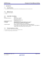
Access address
31
Example of Cache Memory Setting
11 10
432 1 0
Long-word (LW) selection
Tag-address comparison
Entry selection
Address array (ways 0 to 3)
Comparison circuit
Entry 0
Entry 1
·
·
·
·
·
·
·
·
·
·
Entry 127
LW0
LW1
LW2
LW3
16 bytes
×
128 entries
×
4 ways
=
Entry 0 V U Tag address
Entry 1
·
·
·
·
·
·
·
·
·
·
Entry 127
Data array (ways 0 to 3)
8 KB
CMP0 CMP1 CMP2 CMP3
Hit signal (Way 1)
Figure 1 Overview of the Cache-Search Scheme
R01AN0300EJ0101 Rev. 1.01
Oct. 15, 2010
Page 4 of 12
SH7670 Group
2.2
Example of Cache Memory Setting
Procedure for Setting the Module Used
The procedure for setting up the caches is described below.
Cache control register 1 (CCR1) is used to set up the cache. Program code that manipulates the cache control registers
must be executed from an area for which caching is disabled. Also, access to areas for which caching has been enabled
must only proceed after the CCR1 register has been read.
This sample application also changes the interrupt mask to prevent the acceptance of interrupt processing that might
include access to the cache-enabled spaces while the cache mode is being updated.
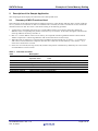
Figure 2 is a flow chart showing an example of the procedure used to enable both the instruction cache and operand
cache.
START
Set the interrupt mask
Set the cache control register 1 (CCR1)
Read the cache control register 1 (CCR1)
Restore the interrupt mask
Store the interrupt mask and set it to level 15 (interrupt disabled)
Set the cache mode (CCR1)
ICF: Set the ICF (instruction cache flush) bit to 1
[Function] Flushes the instruction cache
(its contents are not written back to external memory).
ICE: Set the ICE (instruction cache enable) bit to 1
[Function] Enables the instruction cache.
OCF: Set the OCF (operand cache flush) bit to 1
[Function] Flushes the operand cache
(its contents are not written back to external memory).
WT: Clear the WT (write through) bit to 0
[Function] Set the write-back mode.
OCE: Set the OCE (operand cache enable) bit to 1
[Function] Enables the operand cache.
Restore the interrupt mask
END
Figure 2 Example Flow for Settings Up the Cache
R01AN0300EJ0101 Rev. 1.01
Oct. 15, 2010
Page 5 of 12
SH7670 Group
2.3
Example of Cache Memory Setting
Description of the Sample Program
In the sample program, the instruction cache and operand cache are enabled, and then data equivalent to a single cache
line (16 bytes) are written to external memory (SDRAM) in write-back mode. In this case, the data are actually written
to the cache and not reflected in external memory (SDRAM) until the cache entry (line) is replaced. Contents of
external memory (SDRAM) are read out from a cache-disabled space after the fill operation, and compared with the
contents of the cache.
The section name for the cache manipulation function is adjusted so that the function is placed in a cache-disabled space.
2.4
Procedure for Processing by the Sample Program
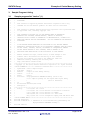
Table 2 describes how the cache is set up by the sample program. Figure 3 shows a flow of processing by the sample
program.
Table 2
Cache Settings
Register Name
Cache control register1
(CCR1)
Address
H'FFFC 1000
Setting
H'0000 0109
Description
ICE = "1":
OCF = "1":
WT = "0":
OCE = "1":
Enables the instruction cache
Flushes the operand cache
Write-back mode
Enables the operand cache
Main function
main
Disable the operand cache:
io_set_cache();
Fill the SDRAM area with 0
Enable the operand cache:
io_set_cache();
Fill the SDRAM area (cached area) with 0 × 55
Compare the values accessed in
a cache-enabled space with the values
accessed in a cache-disabled space
END
Figure 3 Flow of Processing of the Main Function
R01AN0300EJ0101 Rev. 1.01
Oct. 15, 2010
Page 6 of 12
SH7670 Group
2.5
Example of Cache Memory Setting
Allocation of Sections in the Sample Program
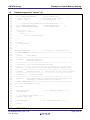
The cache manipulation function must be placed in a cache-disabled space.
In this sample program, an extended compiler function (the #pragma section directive) is used to place the function that
manipulates the cache control registers (io_set_cache) in a specific section (the PCACHE section) separately from the
rest of the program. Linkage editor options are then specified so that only this PCACHE section is allocated to a cachedisabled space. That is, the rest of the program is allocated to a cache-enabled space (the P section).
Figure 4 is a memory map for the sample program.
Internal address
H'0000 0000
H'0000 0000
CS0 (flash memory)
H'0400 0000
H'0000 1000
PResetPRG
PIntPRG
C$BSEC
C$DSEC
P
C
D
PURAM
H'0C00 0000
RP
RC
Reserved
H'0C00 0000
CS3 (SDRAM)
Cacheenabled space
H'1000 0000
CS4
CS5
CS6
Section allocation
DVECTTBL
DINTTBL
Reserved
H'2000 0000
CS0 (flash memory)
H'2400 0000
H'2000 0800
PCACHE
Reserved
H'2C00 0000
CS3 (SDRAM)
H'3000 0000
CS4
CS5
CS6
Cachedisabled space
Reserved
H'FFF8 0000
On-chip SRAM
H'FFF8 0000
RINTTBL
B
R
RPURAM
H'FFF8 7C00
S
H'FFF8 8000
Reserved
H'FFFC 0000
On-chip peripheral modules
Reserved
H'FFFF FFFF
Figure 4 Memory Map of the Sample Program
R01AN0300EJ0101 Rev. 1.01
Oct. 15, 2010
Page 7 of 12
SH7670 Group
3.
3.1
Example of Cache Memory Setting
Sample Program Listing
Sample program list "main.c" (1)
1
/******************************************************************************
2
*
3
*
4
*
This software is supplied by Renesas Electronics Corporation and is only
5
*
intended for use with Renesas products. No other uses are authorized.
6
*
7
*
This software is owned by Renesas Electronics Corporation and is protected under
8
*
all applicable laws, including copyright laws.
9
*
10
*
THIS SOFTWARE IS PROVIDED "AS IS" AND RENESAS MAKES NO WARRANTIES
11
*
REGARDING THIS SOFTWARE, WHETHER EXPRESS, IMPLIED OR STATUTORY,
12
*
INCLUDING BUT NOT LIMITED TO WARRANTIES OF MERCHANTABILITY, FITNESS FOR A
13
*
PARTICULAR PURPOSE AND NON-INFRINGEMENT.
14
*
DISCLAIMED.
15
*
16
*
TO THE MAXIMUM EXTENT PERMITTED NOT PROHIBITED BY LAW, NEITHER RENESAS
17
*
ELECTRONICS CORPORATION NOR ANY OF ITS AFFILIATED COMPANIES SHALL BE LIABLE
18
*
FOR ANY DIRECT, INDIRECT, SPECIAL, INCIDENTAL OR CONSEQUENTIAL DAMAGES
19
*
FOR ANY REASON RELATED TO THIS SOFTWARE, EVEN IF RENESAS OR ITS
20
*
AFFILIATES HAVE BEEN ADVISED OF THE POSSIBILITY OF SUCH DAMAGES.
21
*
22
*
Renesas reserves the right, without notice, to make changes to this
23
*
software and to discontinue the availability of this software.
24
*
By using this software, you agree to the additional terms and
25
*
conditions found by accessing the following link:
26
*
http://www.renesas.com/disclaimer
27
********************************************************************************
28
* Copyright (C) 2007(2010) Renesas Electronics Corporation. All rights reserved.
29
*""FILE COMMENT""*********** Technical reference data **************************
30
*
System Name : SH7671 Sample Program
31
*
File Name
: main.c
32
*
Abstract
: sample of cache memory setting
33
*
Version
: 1.01.03
34
*
Device
: SH7671
35
*
Tool-Chain
: High-performance Embedded Workshop (Ver.4.03.00).
36
*
37
*
38
*
OS
39
*
H/W Platform: M3A-HS71(CPU board)
40
*
Description :
41
********************************************************************************
42
*
43
*
: Jul.09,2007 ver.1.01.00 Revision of the section allocation
44
*
: Jan.17,2008 ver.1.01.01 Revision of comment
45
*
: Feb.28,2008 ver.1.01.02 Revision of a macro name
46
*
: May 10,2010 ver.1.01.03 Changed the company name and device name
47
*""FILE COMMENT END""**********************************************************/
48
#include <machine.h>
49
#include "iodefine.h" /* iodefine.h is a file automatically generated by the
DISCLAIMER
: C/C++ compiler package for the SuperH RISC engine family
:
History
(Ver.9.01 Release01).
: None
: Jul.05,2007 ver.1.00.00
50
51
ALL SUCH WARRANTIES ARE EXPRESSLY
High-performance Embedded Workshop */
#include "defs.h"
R01AN0300EJ0101 Rev. 1.01
Oct. 15, 2010
Page 8 of 12
SH7670 Group
3.2
Example of Cache Memory Setting
Sample program list "main.c" (2)
52
53
/* ==== Prototype declaration
54
void main(void);
==== */
55
56
/* ==== Macro definition ==== */
57
#define SDRAM_ADDR_CACHABLE
(volatile unsigned char *)(0x0C100000)
58
#define SDRAM_ADDR_NON_CACHABLE
(volatile unsigned char *)(0x2C100000)
59
60
/*""FUNC COMMENT""*************************************************************
61
* ID
:
62
* Outline
: Sample Program main
63
*-----------------------------------------------------------------------------
64
* Include
65
*-----------------------------------------------------------------------------
66
* Declaration : void main(void)
67
*-----------------------------------------------------------------------------
68
* Function
: Example of enabling / disabling cache memory.
69
*
: After the SDRAM area has been initialized with the operand cache OFF,
70
*
: a fill operation is performed with the operand cache ON,
71
*
: and the cached area is compared with its shadow in the cache-disabled
: #include "iodefine.h"
space.
72
*
73
*-----------------------------------------------------------------------------
74
* Argument
75
*-----------------------------------------------------------------------------
76
* ReturnValue : void
77
*-----------------------------------------------------------------------------
78
* Notice
: In this sample program, the cache is flushed. Therefore,
79
*
: a program for initialization that enables the cache will invalidate
80
*
: the contents of the cache.
81
*""FUNC COMMENT END""*********************************************************/
: The operand cache is to be controlled.
82
void main(void)
83
{
: void
84
int i;
85
unsigned char *ptr1, *ptr2;
86
87
/* ==== Disabling operand cache ==== */
88
io_set_cache( 0x00000108 );
/* Instruction cache enable
89
* Operand cache flush *
90
* Write-back mode
*
91
* Operand cache disable
*/
92
/* ---- Initializing SDRAM ---- */
93
ptr1 = SDRAM_ADDR_CACHABLE;
94
for(i=0; i<16; i++){
95
*ptr1++ = 0;
96
}
97
/* ==== Enabling operand cache
98
io_set_cache( 0x00000109 );
/* Cache-enabled space
*/
/*
Written to actual memory */
/*
as caching is disabled
*/
==== */
/* Instruction cache enable
99
* Operand cache flush *
100
* Write-back mode
101
* Operand cache enable
R01AN0300EJ0101 Rev. 1.01
Oct. 15, 2010
*
*
*
*/
Page 9 of 12
SH7670 Group
3.3
Example of Cache Memory Setting
Sample program list "main.c" (3)
102
/* ---- Filling SDRAM area
103
ptr1 = SDRAM_ADDR_CACHABLE;
104
for(i=0; i<16; i++){
105
---- */
*ptr1++ = 0x55;
/* Cache-enabled space
*/
/*
Only written to the cache */
/*
in write-back mode
*/
106
}
107
/* ==== Comparing cache-enabled and cache-disabled spaces ==== */
108
ptr1 = SDRAM_ADDR_CACHABLE;
/* Cache-enabled space
*/
109
ptr2 = SDRAM_ADDR_NON_CACHABLE;
/* Cache-disabled space
*/
110
111
for(i=0; i<16; i++){
112
if(*ptr1++ == *ptr2++ ){
113
while(1){
114
/* Error in cache setting
115
116
}
117
}
118
while(1){
119
/* Program end */
120
121
*/
}
}
}
122
123
#pragma section CACHE
124
/*""FUNC COMMENT""*************************************************************
/* Allocated to a non-cacheable area */
125
* ID
:
126
* Outline
: Cache setting
127
*-----------------------------------------------------------------------------
128
* Include
: #include <machine.h>
129
*
: #include "iodefine.h"
130
*-----------------------------------------------------------------------------
131
* Declaration : int io_set_cache(unsigned int mode)
132
*-----------------------------------------------------------------------------
133
* Function
134
*-----------------------------------------------------------------------------
135
* Argument
136
*-----------------------------------------------------------------------------
137
* ReturnValue : 0 : Normally finished
138
*-----------------------------------------------------------------------------
139
* Notice
: This function must be allocated in the CSO non-cacheable area.
140
*
: Interrupts are disabled during cache operation.
141
*""FUNC COMMENT END""*********************************************************/
: Cache is placed in the mode specified by the argument "mode".
: unsigned int mode
142
int io_set_cache(unsigned int mode)
143
{
144
: I : Set the value of cache control register 1
int mask;
145
146
mask = get_imask();
147
set_imask(15);
/* ↓↓↓ interrupts disabled
↓↓↓ */
148
149
/* ==== Setting cache register ==== */
150
CCNT.CCR1.LONG = mode;
151
set_imask(mask);
152
/* ↑↑↑ interrupts disabled
↑↑↑ */
153
154
return 0;
155
}
156
/* End of file */
R01AN0300EJ0101 Rev. 1.01
Oct. 15, 2010
Page 10 of 12
SH7670 Group
4.
Example of Cache Memory Setting
References
• Software Manual
SH-2A/SH2A-FPU Software Manual Rev. 3.00
The latest version of the software manual can be downloaded from the Renesas Electronics website.
• Hardware Manual
SH7670 Group Hardware Manual Rev. 2.00
The latest version of the hardware user's manual can be downloaded from the Renesas Electronics website.
R01AN0300EJ0101 Rev. 1.01
Oct. 15, 2010
Page 11 of 12
SH7670 Group
Example of Cache Memory Setting
Website and Support
Renesas Electronics Website
http://www.renesas.com/
Inquiries
http://www.renesas.com/inquiry
All trademarks and registered trademarks are the property of their respective owners.
R01AN0300EJ0101 Rev. 1.01
Oct. 15, 2010
Page 12 of 12
Revision Record
Rev.
1.00
1.01
Date
Oct.31.08
Oct.15.10
Description
Page
Summary
—
First edition issued
—
Changed the sample program ( AC Switching Characteristics
are removed )
A-1
General Precautions in the Handling of MPU/MCU Products
The following usage notes are applicable to all MPU/MCU products from Renesas. For detailed usage notes on the
products covered by this manual, refer to the relevant sections of the manual. If the descriptions under General
Precautions in the Handling of MPU/MCU Products and in the body of the manual differ from each other, the
description in the body of the manual takes precedence.
1. Handling of Unused Pins
Handle unused pins in accord with the directions given under Handling of Unused Pins in the manual.
⎯ The input pins of CMOS products are generally in the high-impedance state. In operation with an
unused pin in the open-circuit state, extra electromagnetic noise is induced in the vicinity of LSI, an
associated shoot-through current flows internally, and malfunctions occur due to the false
recognition of the pin state as an input signal become possible. Unused pins should be handled as
described under Handling of Unused Pins in the manual.
2. Processing at Power-on
The state of the product is undefined at the moment when power is supplied.
⎯ The states of internal circuits in the LSI are indeterminate and the states of register settings and
pins are undefined at the moment when power is supplied.
In a finished product where the reset signal is applied to the external reset pin, the states of pins
are not guaranteed from the moment when power is supplied until the reset process is completed.
In a similar way, the states of pins in a product that is reset by an on-chip power-on reset function
are not guaranteed from the moment when power is supplied until the power reaches the level at
which resetting has been specified.
3. Prohibition of Access to Reserved Addresses
Access to reserved addresses is prohibited.
⎯ The reserved addresses are provided for the possible future expansion of functions. Do not access
these addresses; the correct operation of LSI is not guaranteed if they are accessed.
4. Clock Signals
After applying a reset, only release the reset line after the operating clock signal has become stable.
When switching the clock signal during program execution, wait until the target clock signal has
stabilized.
⎯ When the clock signal is generated with an external resonator (or from an external oscillator)
during a reset, ensure that the reset line is only released after full stabilization of the clock signal.
Moreover, when switching to a clock signal produced with an external resonator (or by an external
oscillator) while program execution is in progress, wait until the target clock signal is stable.
5. Differences between Products
Before changing from one product to another, i.e. to one with a different type number, confirm that the
change will not lead to problems.
⎯ The characteristics of MPU/MCU in the same group but having different type numbers may differ
because of the differences in internal memory capacity and layout pattern. When changing to
products of different type numbers, implement a system-evaluation test for each of the products.
Notice
1.
All information included in this document is current as of the date this document is issued. Such information, however, is subject to change without any prior notice. Before purchasing or using any Renesas
Electronics products listed herein, please confirm the latest product information with a Renesas Electronics sales office. Also, please pay regular and careful attention to additional and different information to
be disclosed by Renesas Electronics such as that disclosed through our website.
2.
Renesas Electronics does not assume any liability for infringement of patents, copyrights, or other intellectual property rights of third parties by or arising from the use of Renesas Electronics products or
technical information described in this document. No license, express, implied or otherwise, is granted hereby under any patents, copyrights or other intellectual property rights of Renesas Electronics or
others.
3.
You should not alter, modify, copy, or otherwise misappropriate any Renesas Electronics product, whether in whole or in part.
4.
Descriptions of circuits, software and other related information in this document are provided only to illustrate the operation of semiconductor products and application examples. You are fully responsible for
the incorporation of these circuits, software, and information in the design of your equipment. Renesas Electronics assumes no responsibility for any losses incurred by you or third parties arising from the
use of these circuits, software, or information.
5.
When exporting the products or technology described in this document, you should comply with the applicable export control laws and regulations and follow the procedures required by such laws and
regulations. You should not use Renesas Electronics products or the technology described in this document for any purpose relating to military applications or use by the military, including but not limited to
the development of weapons of mass destruction. Renesas Electronics products and technology may not be used for or incorporated into any products or systems whose manufacture, use, or sale is
prohibited under any applicable domestic or foreign laws or regulations.
6.
Renesas Electronics has used reasonable care in preparing the information included in this document, but Renesas Electronics does not warrant that such information is error free. Renesas Electronics
7.
Renesas Electronics products are classified according to the following three quality grades: "Standard", "High Quality", and "Specific". The recommended applications for each Renesas Electronics product
assumes no liability whatsoever for any damages incurred by you resulting from errors in or omissions from the information included herein.
depends on the product's quality grade, as indicated below. You must check the quality grade of each Renesas Electronics product before using it in a particular application. You may not use any Renesas
Electronics product for any application categorized as "Specific" without the prior written consent of Renesas Electronics. Further, you may not use any Renesas Electronics product for any application for
which it is not intended without the prior written consent of Renesas Electronics. Renesas Electronics shall not be in any way liable for any damages or losses incurred by you or third parties arising from the
use of any Renesas Electronics product for an application categorized as "Specific" or for which the product is not intended where you have failed to obtain the prior written consent of Renesas Electronics.
The quality grade of each Renesas Electronics product is "Standard" unless otherwise expressly specified in a Renesas Electronics data sheets or data books, etc.
"Standard":
Computers; office equipment; communications equipment; test and measurement equipment; audio and visual equipment; home electronic appliances; machine tools;
personal electronic equipment; and industrial robots.
"High Quality": Transportation equipment (automobiles, trains, ships, etc.); traffic control systems; anti-disaster systems; anti-crime systems; safety equipment; and medical equipment not specifically
designed for life support.
"Specific":
Aircraft; aerospace equipment; submersible repeaters; nuclear reactor control systems; medical equipment or systems for life support (e.g. artificial life support devices or systems), surgical
implantations, or healthcare intervention (e.g. excision, etc.), and any other applications or purposes that pose a direct threat to human life.
8.
You should use the Renesas Electronics products described in this document within the range specified by Renesas Electronics, especially with respect to the maximum rating, operating supply voltage
range, movement power voltage range, heat radiation characteristics, installation and other product characteristics. Renesas Electronics shall have no liability for malfunctions or damages arising out of the
use of Renesas Electronics products beyond such specified ranges.
9.
Although Renesas Electronics endeavors to improve the quality and reliability of its products, semiconductor products have specific characteristics such as the occurrence of failure at a certain rate and
malfunctions under certain use conditions. Further, Renesas Electronics products are not subject to radiation resistance design. Please be sure to implement safety measures to guard them against the
possibility of physical injury, and injury or damage caused by fire in the event of the failure of a Renesas Electronics product, such as safety design for hardware and software including but not limited to
redundancy, fire control and malfunction prevention, appropriate treatment for aging degradation or any other appropriate measures. Because the evaluation of microcomputer software alone is very difficult,
please evaluate the safety of the final products or system manufactured by you.
10. Please contact a Renesas Electronics sales office for details as to environmental matters such as the environmental compatibility of each Renesas Electronics product. Please use Renesas Electronics
products in compliance with all applicable laws and regulations that regulate the inclusion or use of controlled substances, including without limitation, the EU RoHS Directive. Renesas Electronics assumes
no liability for damages or losses occurring as a result of your noncompliance with applicable laws and regulations.
11. This document may not be reproduced or duplicated, in any form, in whole or in part, without prior written consent of Renesas Electronics.
12. Please contact a Renesas Electronics sales office if you have any questions regarding the information contained in this document or Renesas Electronics products, or if you have any other inquiries.
(Note 1)
(Note 2)
"Renesas Electronics" as used in this document means Renesas Electronics Corporation and also includes its majority-owned subsidiaries.
"Renesas Electronics product(s)" means any product developed or manufactured by or for Renesas Electronics.
http://www.renesas.com
SALES OFFICES
Refer to "http://www.renesas.com/" for the latest and detailed information.
Renesas Electronics America Inc.
2880 Scott Boulevard Santa Clara, CA 95050-2554, U.S.A.
Tel: +1-408-588-6000, Fax: +1-408-588-6130
Renesas Electronics Canada Limited
1101 Nicholson Road, Newmarket, Ontario L3Y 9C3, Canada
Tel: +1-905-898-5441, Fax: +1-905-898-3220
Renesas Electronics Europe Limited
Dukes Meadow, Millboard Road, Bourne End, Buckinghamshire, SL8 5FH, U.K
Tel: +44-1628-585-100, Fax: +44-1628-585-900
Renesas Electronics Europe GmbH
Arcadiastrasse 10, 40472 Düsseldorf, Germany
Tel: +49-211-6503-0, Fax: +49-211-6503-1327
Renesas Electronics (China) Co., Ltd.
7th Floor, Quantum Plaza, No.27 ZhiChunLu Haidian District, Beijing 100083, P.R.China
Tel: +86-10-8235-1155, Fax: +86-10-8235-7679
Renesas Electronics (Shanghai) Co., Ltd.
Unit 204, 205, AZIA Center, No.1233 Lujiazui Ring Rd., Pudong District, Shanghai 200120, China
Tel: +86-21-5877-1818, Fax: +86-21-6887-7858 / -7898
Renesas Electronics Hong Kong Limited
Unit 1601-1613, 16/F., Tower 2, Grand Century Place, 193 Prince Edward Road West, Mongkok, Kowloon, Hong Kong
Tel: +852-2886-9318, Fax: +852 2886-9022/9044
Renesas Electronics Taiwan Co., Ltd.
7F, No. 363 Fu Shing North Road Taipei, Taiwan, R.O.C.
Tel: +886-2-8175-9600, Fax: +886 2-8175-9670
Renesas Electronics Singapore Pte. Ltd.
1 harbourFront Avenue, #06-10, keppel Bay Tower, Singapore 098632
Tel: +65-6213-0200, Fax: +65-6278-8001
Renesas Electronics Malaysia Sdn.Bhd.
Unit 906, Block B, Menara Amcorp, Amcorp Trade Centre, No. 18, Jln Persiaran Barat, 46050 Petaling Jaya, Selangor Darul Ehsan, Malaysia
Tel: +60-3-7955-9390, Fax: +60-3-7955-9510
Renesas Electronics Korea Co., Ltd.
11F., Samik Lavied' or Bldg., 720-2 Yeoksam-Dong, Kangnam-Ku, Seoul 135-080, Korea
Tel: +82-2-558-3737, Fax: +82-2-558-5141
© 2010 Renesas Electronics Corporation. All rights reserved.
Colophon 1.0