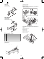
1
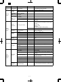
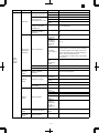
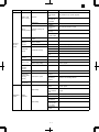
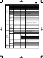
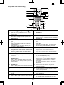
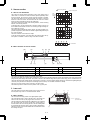
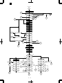
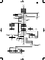
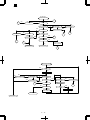
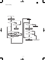
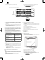
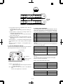
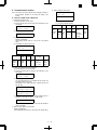
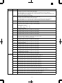
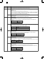
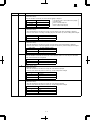
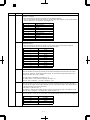
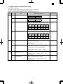
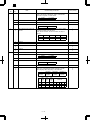
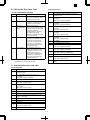
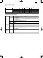
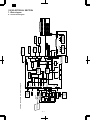
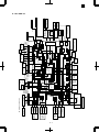
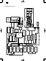
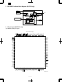
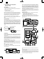
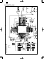
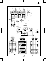
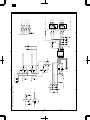
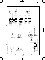
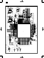
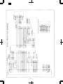
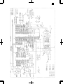
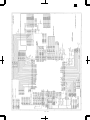
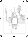
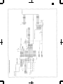
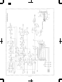
AR-F152
Output Signals
A16 ∼ A23 ∗ High-Order Address Bits.
These are the most significant 8 bits of the memory address bus.
HBE
∗ High Byte Enable.
Status signal used to enable data transfers on the most
significant byte of the data bus.
ST0 ∼ 3
Status.
Not used.
U/S
User/Supervisor.
Not used.
ILO
Interlocked Operation.
Not used.
HLDA
Hold Acknowledge.
Activated by the CPU in response to the HOLD input to indicate CPU has released the bus.
PFS
Program Flow Status.
A pulse on this signal indicates the beginning of execution
of instruction.
BPU
BPU Cycle.
Not used.
RSTO
Reset Output.
This signal becomes active when RSTI is low, initiating a
system reset.
RD
Read Strobe.
Activated during CPU or DMA read cycles to enable reading of data from memory or peripherals.
WR
Write Strobe.
Activated during CPU or DMA write cycles to enable writing of data to memory or peripherals.
TSO
Timing State Output.
Not used.
DBE
Data Buffers Enable.
Used to control external data buffers. It is active when the
data buffers are to be enabled.
OSCOUT Crystal Output.
Not used.
IAS
SPecial Cycle Address Strobe.
Not used.
CTTL1 – 2 System Clock.
Output clock for bus timing. CTTL1 and CTTL2 must be
externally connected together.
FCLK
Fast Clock.
Not used.
ALE
Address Latch Enable.
Active high signal that can be used to control external address latches.
IOUT
Interrupt Output
Not used.
(3) LC8213K (IC505) Pin Layout
I:
O:
B:
P:
NC:
Input pin
Output pin
Bidirectional pin
Power pin
Not connected
No.
Pin name
Type
No.
Pin name
Type
1
CS
I
41
AEN
O
2
RD
I
42
AST
O
3
WR
I
43
MDEN
O
4
A2
I
44
MRD
O
5
A1
I
45
MWR
O
O
6
A0
I
46
IORD
7
VDD
P
47
IOWR
O
NC
48
LDE
O
O
8
9
D7
B
49
UDE
10
D6
B
50
READY
I
11
D5
B
51
DTC
O
12
D4
B
52
VSS
13
VSS
P
53
14
D3
B
54
MA23
O
15
D2
B
55
MA22
O
16
D1
B
56
MA21
O
17
D0
P
NC
B
57
MA20
O
18
NC
58
MA19
O
19
NC
59
MA18
O
20
IREQ
O
60
MA17
O
21
DREQ
O
61
MA16
O
22
DACK
I
62
MA/MD15
O
23
NC
63
VSS
P
24
NC
64
MA/MD14
B
25
NC
65
MA/MD13
B
26
NC
66
MA/MD12
B
I
67
MA/MD11
B
27
RESET
28
CLK
I
68
MA/MD10
B
29
VSS
P
69
MA/MD9
B
30
TEST4
I
70
MA/MD8
B
Input-Output Signals
31
VDD
P
71
MA/MD7
B
AD0 ∼ 15
32
TEST3
I
72
VSS
P
33
TEST2
I
73
VDD
P
34
TEST1
I
74
MA/MD6
B
35
TEST0
I
75
MA/MD5
B
NC
76
MA/MD4
B
O
77
MA/MD3
B
SPC
DDIN
ADS
* Address/Data Bus.
Multiplexed Address/Data Information. Bit 0 is the least
significant bit of each.
Slave Processor Control.
Not used.
* Data Direction.
Status signal indicating the direction of the data transfer
during a bus cycle. During HOLD acknowledge this signal
becomes an input and determines the activation of RD or
WR.
* Address Strobe
Controls address latches; signals the beginning of a bus
cycle. During HOLD acknowledge this signal becomes an
input and the CPU monitors it to detect the beginning of
a DMA cycle and generate the relevant strobe signals.
When a DMA is used, ADS should be pulled up to VCC
through a 10 kΩ resistor.
12 – 16
36
37
BREQ
38
BACK
I
78
MA/MD2
B
39
IDREQ
I
79
MA/MD1
B
40
IDACK
O
80
MA/MD0
B