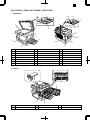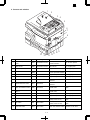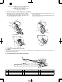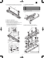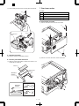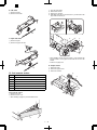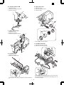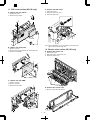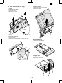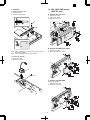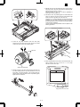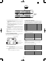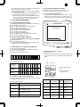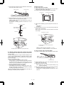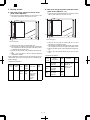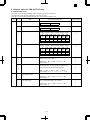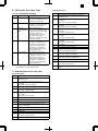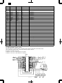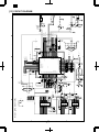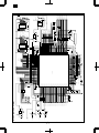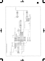
1
AR-F152 CODE: 00ZARF152/A1E DIGITAL COPIER (AR-F152) MODEL AR-151 AR-156 AR-F152 CONTENTS [ 1 ] GENERAL . . . . . . . . . . . . . . . . . . . . . . . . . . . 1 - 1 [ 2 ] SPECIFICATIONS . . . . . . . . . . . . . . . . . . . . . . 2 - 1 [ 3 ] CONSUMABLE PARTS . . . . . . . . . . . . . . . . . . . 3 - 1 [ 4 ] EXTERNAL VIEWS AND INTERNAL STRUCTURES . . . 4 - 1 [ 5 ] UNPACKING AND INSTALLATION . . . . . . . . . . . . . 5 - 1 [ 6 ] OPERATIONAL DESCRIPTIONS . . . . . . . . . . . . . . 6 - 1 [ 7 ] DISASSEMBLY AND ASSEMBLY . . . . . . . . . . . . . . 7 - 1 [ 8 ] ADJUSTMENTS . . . . . . . . . . . . . . . . . . . . . . . 8 - 1 [ 9 ] SIMULATION, FAX SOFTWARE SWITCH, TROUBLE CODES . . . . . . . . . . . . . . . . . . . . . . 9 - 1 [10] USER PROGRAM . . . . . . . . . . . . . . . . . . . . . . 10 - 1 [11] MAINTENANCE . . . . . . . . . . . . . . . . . . . . . . . . 11 - 1 [12] ELECTRICAL SECTION . . . . . . . . . . . . . . . . . . . 12 - 1 [13] CIRCUIT DIAGRAM . . . . . . . . . . . . . . . . . . . . . 13 - 1 Parts marked with “ ” are important for maintaining the safety of the set. Be sure to replace these parts with specified ones for maintaining the safety and performance of the set. SHARP CORPORATION This document has been published to be used for after sales service only. The contents are subject to change without notice. AR-F152 CAUTION This product is a class 1 laser product that complies with 21CFR 1040.10 and 1040.11 of the CDRH standard and IEC825. This means that this machine does not produce hazardous laser radiation. The use of controls, adjustments or performance of procedures other than those specified herein may result in hazardous radiation exposure. This laser radiation is not a danger to the skin, but when an exact focusing of the laser beam is achieved on the eye’s retina, there is the danger of spot damage to the retina. The following cautions must be observed to avoid exposure of the laser beam to your eyes at the time of servicing. 1) When a problem in the laser optical unit has occurred, the whole optical unit must be exchanged as a unit, not as individual parts. 2) Do not look into the machine with the main switch turned on after removing the developer unit, toner cartridge, and drum cartridge. 3) Do not look into the laser beam exposure slit of the laser optical unit with the connector connected when removing and installing the optical system. 4) The middle frame contains the safety interlock switch. Do not defeat the safety interlock by inserting wedges or other items into the switch slot. CAUTION INVISIBLE LASER RADIATION, WHEN OPEN AND INTERLOCKS DEFEATED. AVOID EXPOSURE TO BEAM. VORSICHT UNSICHTBARE LASERSTRAHLUNG, WENN ABDECKUNG GEÖFFNET UND SICHERHEITSVERRIEGELUNG ÜBERBRÜCKT. NICHT DEM STRAHL AUSSETZEN. VARO ! AVATTAESSA JA SUOJALUKITUS OHITETTAESSA OLET ALTTIINA NÄKYMÄTTÖMÄLLE LASERSÄTEILYLLE ÄLÄ KATSO SÄTEESEEN. ADVARSEL USYNLIG LASERSTRÅLNING VED ÅBNING, NÅR SIKKERHEDSBRYDERE ER UDE AF FUNKTION. UNDGÅ UDSAETTELSE FOR STRÅLNING. VARNING ! LASER WAVE – LENGTH : 780 ∼ 795 Pulse times : 0.481 ms/6 mm Out put power : 0.20 ± 0.03 mW OSYNLIG LASERSTRÅLNING NÄR DENNA DEL ÄR ÖPPNAD OCH SPÄRREN ÄR URKOPPLAD. BETRAKTA EJ STRÅLEN. – STRÅLEN ÄR FARLIG. AR-F152 At the production line, the output power of the scanner unit is adjusted to 0.57 MILLI-WATT PLUS 20 PCTS and is maintained constant by the operation of the Automatic Power Control (APC). Even if the APC circuit fails in operation for some reason, the maximum output power will only be 15 MILLI-WATT 0.1 MICRO-SEC. Giving an accessible emission level of 42 MICRO-WATT which is still-less than the limit of CLASS-1 laser product. Caution This product contains a low power laser device. To ensure continued safety do not remove any cover or attempt to gain access to the inside of the product. Refer all servicing to qualified personnel. VAROITUS! LAITTEEN KÄYTTÄMINEN MUULLA KUIN TÄSSÄ KÄYTTÖOHJEESSA MAINITULLA TAVALLA SAATTAA ALTISTAA KÄYTTÄJÄN TURVALLISUUSLUOKAN 1 YLITTÄVÄLLE NÄKYMÄTTÖMÄLLE LASERSÄTEILYLLE. VARNING - OM APPARATEN ANVÄNDS PÅ ANNAT SÄTT ÄN I DENNA BRUKSANVISNING SPECIFICERATS, KAN ANVÄNDAREN UTSÄTTAS FÖR OSYNLIG LASERSTRÅLNING, SOM ÖVERSKRIDER GRÄNSEN FÖR LASERKLASS 1. The foregoing is applicable only to the 220V model, 230V model and 240V model. LUOKAN 1 LASERLAITE KLASS 1 LASER APPARAT AR-F152 [1] GENERAL 1. AR-151/156/F152 major functions Item CPM SB/MB 2 tray SPF AR-151 15CPM MB Opt ∗1 Opt AR-156 15CPM MB AR-F152 15CPM MB R-SPF FAX GDI with USB ∗1 Opt Opt Model Opt GDI without USB SOPM Duplex Opt ∗2 Opt Descriptions of items CPM: Copy speed (Copies Per Minute) SB/MB: SB = Manual feed single bypass, MB = Manual feed multi bypass 2 tray: Second cassette unit. The 1 tray unit (AR-DE9) is optionally available. SPF: Original feed unit R-SPF: Duplex original feed unit FAX: FAX function. The AR-FX3 (FAX-SPF and FAX board) is optionally available.) GDI with USB: GDI printer function with USB. The AR-PG1 (GDI + USB kit) is optionally available. GDI without USB: GDI printer function without USB. The said model has no option of it. SOPM: Scan One Print Many function (Many copies are made by one scan.) Duplex: Auto duplex copy function Descriptions of table : Standard provision : No function or no option available ∗1: Incompatible between SPF and FAX function ∗2: 1 tray option for Europe 2. System Configuration (AR-F152) (AR-151) (AR-156) (Options) AR-DE9 AR-SP3 AR-PG1 AR-FX3 1 – 1 AR-F152 [2] SPECIFICATIONS 1. Basic specifications of copier A. Basic specifications Item Spec. Type Desktop Copy system Dry, electrostatic Segment (class) Digital personal copier AR-151: 518mm × 482.6mm × 292.6mm AR-156: 518mm × 482.6mm × 379mm AR-F152: 518mm × 482.6mm × 465.3mm External dimensions (W × D × H) (mm) AR-151: Approx. 19Kg, (drum cartridges included) AR-156: Approx. 22Kg, (drum cartridges included) AR-F152: Approx. 25Kg, (drum cartridges included) Weight B. Operation specification Section Item Details Spec. AR-151/AR-156: 1 tray (250 sheets) + multi bypass (50 sheets) AR-F152: 2 tray (250 sheets) + multi bypass (50 sheets) (1 tray for Europe) Paper feed system Paper size Tray paper feed section A4, B5, A5 (Landscape) 56 – 80g/m2 Paper weight Paper feed capacity Kinds Standard paper, specified paper, recycled paper Remark AB system User adjustment of paper guide available Paper size A4, B5, A5, B6, A6 (Landscape) 52 – 128g/m2 Paper weight Multi bypass paper feed section Paper feed section Paper feed capacity Kinds ∗1 Remark User adjustment of paper guide available 8-1/2″ × 14″, 8-1/2 × 11″, 8-1/2″ × 5-1/2″ (Landscape) Paper weight 15 – 21 lbs. Paper feed capacity Kinds User adjustment of paper guide available 8-1/2″ × 14″, 8-1/2 × 11″, 8-1/2″ × 5-1/2″, 3-1/2″ × 5-1/2″ (Landscape) Paper size Multi bypass paper feed section Paper weight 14 – 34.5 lbs. Paper feed capacity 50 sheets Kinds ∗1 Standard paper, specified paper, recycled paper, OHP, Label, Postal card Remark User adjustment of paper guide available Paper size A4, B5, A5 (Landscape) 56 – 80 g/m2 Paper weight AB system Paper for Duplex (AR-156 only) 250 sheets Standard paper, specified paper, recycled paper Remark Inch system 50 sheets Standard paper, specified paper, recycled paper, OHP, Label, Postal card Paper size Tray paper feed section 250 sheets Standard paper, Specified paper, Recycled paper Kinds 8-1/2″ × 14″, 8-1/2″ × 11″, 8-1/2″ × 5-1/2″ (Landscape) Paper size Paper weight 15-21 lbs Inch system Standard paper, Specified paper, Recycled paper Kinds ∗1: OHP, Label, Postal card: each 1 pc. 2 – 1 AR-F152 Section Paper exit section Item Details Spec. Exit way Face down Capacity of output tray 100 sheets Original set Center Registration (left edge) B4 (10″ × 14″) Max. original size Originals Original kinds sheet Original size detection None Scanning system CCD sensor Optical section Scanning section CCD sensor scanning by lighting lamp scanner Resolution 400 dpi Type Lighting lamp Xenon lamp Voltage 1.5kV 11 ± 3W Power consumption Gradation Writing section 256 gradations/8bit Writing system Writing to OPC drum by the semiconductor laser Laser unit Resolution Photoconductor 600 dpi Type OPC (30φ) Life Image forming 18k Charging system Saw -tooth charging with a grid, / (–) scorotron discharge Transfer system (+) DC corotron system Separation system (–) DC corotron system Developing Developing system Dry, 2-component magnetic brush development system Cleaning Cleaning system Charger Counter blade system (Counter to rotation) Fusing system Fusing section Heat roller system Upper heat roller Type Teflon roller Lower heat roller Type Silicon rubber roller Type Halogen lamp Heater lamp Voltage 100V Power consumption 800W Voltage Power source Local AC voltage Frequency Common use for 50 and 60Hz Max. Electrical section AR-151/AR-156: 1000W, AR-F152: 1000W Average (during copying) *1) Power consumption Average (stand-by) *1) Pre-heat mode * AR-151/AR-156: 310Wh/H, AR-F152: 310Wh/H AR-151/AR-156: 70Wh/H, AR-F152: 90Wh/H 1) AR-151/AR-156: 40Wh/H, AR-F152: 51Wh/H 1) Auto power shut-off mode * AR-151/AR-156: 18Wh/H, AR-F152: 23Wh/H *1) May fluctuate due to environmental conditions and the input voltage. C. Copy performance Section Copy magnification Item Details Spec. 3R + 2E (AB system: 50, 70, 81, 100, 141, 200%) (Inch system: 50, 64, 78, 100, 129, 200%) Fixed magnification ratios 50 ∼ 200% (151 steps in 1% increments) Zooming magnification ratios Manual steps (manual, photo) 5 steps 2 – 2 AR-F152 Section Item Details Spec. 9.6 sec. or below (A4), 9.4 sec. or below (8-1/2" × 14") (Pre-heat mode: 16 sec. or below / Auto powershut-off mode: 23 sec. or below) Tray paper feed Copy speed First copy time 10.0 sec (Pre-heat mode: 16 sec. or below / Auto power-shut-off mode: 23 sec. or below) Manual paper feed AB system: A4 (Landscape) B5 (Landscape) Inch system 8-1/2″ × 14″ (Landscape) 8-1/2″ × 11″ (Landscape) Copy speed (CPM) Copy speed (CPM) Copy speed (CPM) Copy speed (CPM) Same size 15 Enlargement 15 Reduction 15 Same size 15 Enlargement 15 Reduction 15 Same size 12 Enlargement 12 Reduction 12 Same size 15 Enlargement 15 Reduction 15 Max. continuous copy quantity 99 Leading edge 1 ∼ 4mm Trailing edge 4mm or less, 6mm or less (Duplex copying/both images) Void area Side edge void area 4.0mm or less (per side), 4.5mm or less (Duplex copying/both images: per side) machine with side edge void 0.5mm ∼ 4mm (Total of both edge voids) OC mode Leading edge Same size: 3.0mm or less / Enlarge (200%): 2.0mm or less / Reduction (50%): 6.0mm or less SPF/R-SPF/ Duplex Leading edge Same size: 4.0mm or less / Enlarge (200%): 3.0mm or less / Reduction (50%): 8.0mm or less Void Image loss Warm-up time 0 sec. Power save mode reset time 0 sec. Paper jam recovery time 0 sec. 2. Basic specifications of facsimile (AR-F152 only) Large Item Middle Item CommuniTransmission cation system method Scanning system Document size Small Item Sub Item Spec. Transmission time Approx. 6 sec. (G3 ECM/14,400bps) Transmission Method V17, V29, V27TER, V33 (Only Receiving) Compression method MH, MR, MMR Modem speed 14,400bps → 2,400bps automatic fall back Mutual transmission G3 Line used Public Switched Telephone Network (PSTN), Private Branch exchange (PBX), Number of lines used 1 line (cannot be added) ECM YES Max. document width OC: B4 Unscannable region Leading edge 1 to 4 mm, trailing edge: 4mm max., left end + right end: either 4mm max. Transmitted document size SPF: Max. 10.1" × 19.7" SPF: Min. 8.5" × 5.5"(Inch System) SPF: 210 × 148mm (AB system) Document size designation B4, 8-1/2, A4, B5, A5, 5/2 Two-sided document designation NO 2 – 3 SPF: B4 (Multi)/ 257 × 500 (Single) AR-F152 Large Item Scanning system Scanning system Middle Item Sub Item Long document 500 mm (Single Feed with hand hold) Automatic document detection SPF YES (Over or Under B4 size) OC NO Transmission mode SPF/OC transmission changeover NO Document loading capacity, scanning cycle (SPF performance) Continuous, automatic feed compatibility NO Document loading capacity SPF: 30 sheets Document scanning cycle 13 sheets/min. (Standard mode, A4R memory transmission) Equivalent to 256 scales Following functions are not possible in half-Tone mode in B4 size. ● Timer sending ● Memory sending ● Broadcast ● To store the original for memory polling. Half tone (photo mode) Resolution 8 dot /mm × 7.7 line / mm (Fixed) Contrast adjustment Contrast selection Standard 8 dot / mm × 3.85 line / mm Resolution selection Fine 8 dot / mm × 7.7 line / mm Super fine 8 dot / mm × 15.4 line / mm Finest NO Manual in 3 stages (AE) Printer section resolution Printing size Print system Print paper Transmission function system Spec. Document size Half tone reproduction Image processing system Small Item Easy dialing function Time designation function 600dpi Max. printing width 215.9 mm Print paper size detection YES (Only width): A4/Letter or small size Printing size A4/Letter/Legal Cassette capacity 250 × 2 (1 tray option for Europe) Print paper absence detection By failing paper pick up Exit Paper Tray Full sensor NO Feed Paper cassette Rapid key dialing 20 other parties Speed dialing 100 other parties Group dialing 20 groups (including the other parties registered to rapid key dialing) Phonebook transmission By using the SEARCH key: Any other parties registered to speed dialing and rapid key dialing can be searched for using the first letter. Chain dialing YES Redialing The last number dialed is saved Program NO Mode recall NO Time specified transmission/polling Time of day specified for transmission or polling. Max.3 2 – 4 AR-F152 Large Item Middle Item Small Item Automatic recall mode when other party is busy Recall mode when communication error occurs Recall mode Memory Transmission/direct transmission Sub Item Spec. Intervals 1 to 15 minutes Count 1 to 14 times/0: no re-transmission Intervals 1 to 15 minutes Count 1 to 14 times/0: no re-transmission Transmitted Pages Beginning with the page where error occurred Number of transmissions counted in recall mode simultaneously Max. 20 transmissions Subsequent transmission reservation override in recall mode YES Memory Transmission YES Number of transmission Reservations that can be made Max. 20 Transmission is cancelled when using Timer, Group or Broadcast function. Only scanned’ data is transmitted. Memory transmission Processing when memory is full ∗ The number of pages to be actually sent does not always correspond to the one passing through the SPF in case of communication error. ∗ The transmission is cancelled when communication error occurs. Transmission function system Setting change After Transmission Setting Line sound monitoring function Broadcast function Direct transmission YES Default setting By Memory All Clear Dialing confirmation monitoring YES (Service Man diagnostic.) Broadcast transmission Number of destinations 50 destinations (Including the Group Dial) Transmission method Broadcast key, group key Usable numbers Rapid or Speed keys Transmitted to group registered to rapid keys or speed dial. Group dialing Boadcast function NO Relay transmission Confidential function Confidential transmission Batch transmission function Batch transmission Instructing Station NO Relay station NO Multiple relay NO Number of relay groups NO Number of Receiving stations that may be Specified per Group NO Other party’s Station NO NO 2 – 5 AR-F152 Large Item Middle Item Priority function Transmission function system Small Item Sub Item Spec. Transmission reservation interrupt NO Broadcast interrupt NO Recall mode interrupt NO Multiple message transmission function Multiple message transmission NO Rotational Transmission Rotational transmission Book document transmission Book document transmission OK stamp Remote transmission (Memory Polling) Remote transmission (polling transmission function) Protective function Paper size NO Transmission method YES (From OC mode) Consecutive page transmission (page splitting) NO OK stamp NO Remote Transmission YES (From Memory) Check by other Party’s number NO Check by Matching of System number (user’s own machine) and ID number (other party’s Machine) (between Sharp machines only) NO Automatic receiving (can be switched to A.M mode or manual receiving in key operator program) Default setting Number of calls Receiving mode 0 to 9 times (factory-set to twice: can be changed in key operator program) - The external telephone rings once if set the number of calls for automatic receiving to 0 times. Automatic receiving Automatic phone/fax switching NO Manual receiving Manual receiving setting YES Manual receiving Number of Switching calls to automatic Receiving in manual receiving mode OFF/1 to 9 times Answering Machine mode YES Receiving function system Receiving mode Telephone message receiver connection Automatically switch to ON / OFF automatic receive Quiet detect time Receiving mode timer switching OFF/ 1 to 9 sec. NO 2 – 6 AR-F152 Large Item Middle Item Variable scale factor receiving Small Item Reduction Sub Item YES (ON/OFF in key operator program) By received data print size Designation YES Enlargement Memory Substitute receiving into receiving function memory Transfer Receiving function system Number specified receiving NO Substitute Receiving into Memory Only when data cannot be output Forced memory receiving NO Received data override Output NO Transfer at occurrence of trouble YES Receiving of only specified number enabled NO Anti junk fax mode YES (ON/OFF) 10 group, 20 letters Sender Confidential function Confidential receiving NO Mailbox name NO Confidential ID code NO NO Split size YES Split receiving setting YES (according to paper selection condition in key operator program) Split receiving Two-sided document receiving NO 2-in-1 receiving NO Transmission request Transmission Request YES Resolution at transmission Request Depends on the Sending Machine. Turnaround transmission NO Speed dialing Registration system NO Mailbox Rotational receiving Transmission request (polling receiving function) Spec. Reduction made within Regular size Number registration Speed dialing Number of other parties 100 other parties Number of other party’s Number digits 20 digits Registered name 20 letters (may be omitted) Searched letters Up to 1 letter User tag Classification NO International communication mode setting NO Transmission method Speed dialing key + (00 to 99) + start key 2 – 7 AR-F152 Large Item Middle Item Small Item Rapid key dialing Number registration Group dialing Registration system Sub Item Spec. Number of other parties 20 other parties Number of other party’s Number digits 20 digits Registered name 20 letters (may be omitted) Searched letters Up to 1 letter User tag Classification NO International communication mode setting NO Transmission method Rapid key dialing Registration keys Rapid keys Max. number of registered other parties per group 50 other parties Registrable Number Numbers registered to speed dialing and rapid key dialing. Registered name 20 letters (may be omitted) Searched letters NO User tag Classification NO Transmission method Group dialing Number of programs NO Registerable item NO Program Registered name NO Calling method NO Setting change After calling NO Registration key NO Number of other parties NO Registration method NO Sender’s name 24 letters, registered in key operator program Sender’s number 20 digits, registered in key operator program Transmission request enable number Transmission Request source Number Registration NO System number System number Registration NO ID number ID number Registration NO Batch Sender Registration Transmission request/remote transmission enable number registration Letter input Sender registration Input method Key input YES Letters that may be input Characters Alphanumeric characters, symbols Registered data read-out, read-in NO Date & time adjustment Registered in key operator program Support terms is from 1990 to 2089. Date indication change NO Backup Registered data backup at power failure SRAM used, built-in battery-backed 2 – 8 AR-F152 Large Item Middle Item Small Item Sub Item Handset Telephone Function System On-hook YES Hold NO Pause YES (2 second fixed) Phone transmission at power failure NO Ringer volume Adjusted in key operator program Speaker volume Adjusted by pressing arrow keys on the fax control panel Tone pulse switching Switched between 10 pps and TONE in key operator program (North America) External telephone connection YES Automatic telephone/fax switching Memory capacity Remote receiving switching YES (switching number in 1 digit +**) 0 to 9 NO Audio response NO Response voice recording NO Standard 2MB (Approx. 120 pages/A4) Option NO Yes Job memory back up: Approx. 1 hour (after min. 6 minutes charge) Configuration Memory back up to 5 years. Memory Back up Fax Memory Memory Contents (transmission reservation) confirmation LCD indication NO Print out YES Memory remain indication YES (Memory available percent display 3 digits in % on LCD Page counter NO Date printing YES (Year: month: day/ year in 4 digits) LCD: 2 digits / Print: 4 digits Date indication change Additional information printing function for transmission Cover function Transmission message Sender printing function Additional printing function for receiving Spec. NO Cover item NO Other party’s name YES Other party’s number YES Sender’s name YES Sender’s number YES Transmission message YES Regular message NO MESSAGE/URGENT/ IMPORTANT/CONFIDENTIAL/PLS.DISTRIBUTE/PLS. CALL BACK User message NO Sender’s number 20 digits Sender’s name 24 letters Index printing YES 2 – 9 AR-F152 Large Item Middle Item Communication record function Record table system Communication result report function Other report/list Other party confirmation function CSI function Others Department management Operation panel display Small Item Sub Item Spec. Communication record table size A4, LETTER, Legal (not output if size setting is not A4, LETTER, legal or larger) Communication record memory capacity 50 communications for transmission/receiving respectively Communication record table Number of communications 50 communications for transmission/receiving respectively Time-specified output YES 5 kinds, Every day, Each 2 day, Each 4 day, Once a week, OFF The print time is fixed at 00:00. When recording Memory is full NO Printing sequence LAST IN LAST OUT Department-bydepartment output NO Time-specified communication table Common to transmission record table Confidential receiving confirmation table NO Communication result table (transmission) YES (ALWAYS PRINT, ERROR/ TIMER, SEND ONLY, NEVER PRINT, ERROR ONLY) Broadcast transmission report NO Communication result table (receiving) YES Document image printing when memory transmission is not yet made NO Rapid key dialing list YES (output as telephone number list) Speed dialing list YES (output as telephone number list) Group dialing list YES Transmission activity list YES ID/sender list NO Batch transmission confirmation list NO Confidential ID list NO Option setting list YES Telephone list YES Timer list YES Anti junk fax number list YES Receptions activity List YES Memory image erasure list NO Other party confirmation display NO CSI YES Department-by-department user restriction NO Number of set departments NO Department-by-department charge management function NO LCD 20 letters by 2 lines 2 – 10 AR-F152 Large Item Others Middle Item Small Item Sub Item Spec. Auto startup mode NO Distinctive Ring (Only North America and Australia) YES Power consumption Energy star compatibility YES Automatic Summer Set (Only Europe) YES PBX setting (Only Europe) YES 2 – 11 AR-F152 [3] CONSUMABLE PARTS 1. Supply system table A. SEC governments No. 1 Name Toner CA(Black) with IC Content Toner (Toner :Net Weight 210g) Polyethylene bag Life × 10 65K Product name AR-152MT-J Package 1 × 10 Remark ∗ Life setup is based on A4 6%. MT=NT∗10 B. SEC/SECL/LAG No. Name Content Life Product name Package Remark 1 Toner CA(Black) with IC Toner (Toner :Net Weight 210g) Polyethylene bag × 10 65K AR-152MT 1 ∗ Life setup is based on A4 6%. MT=NT∗10 2 Developer Developer (Developer: Net Weight 170g) × 10 250K AR-152MD 1 MD=ND∗10 3 Drum kit Drum Drum fixing plate AR-152DR 10 × 10 × 1 × 1 25K Note: Printing of the master/individual cartons is made in 2 languages, English/French. Packed together with the machine: DR 25K/Developer UN/Process UN C. Europe subsidiaries/East Europe/SCA/SCNZ No. 1 Name Toner CA(Black) with IC Content Life Product name Package Remark Toner (Toner :Net Weight 210g) Polyethylene bag × 10 65K AR-152LT 1 LT=T∗10 × 10 250K AR-152LD 1 LD=DV∗10 AR-152DM 10 2 Developer Developer (Developer :Net Weight 170g) 3 Drum kit Drum Drum fixing plate × 10 × 1 × 1 25K Note: Printing of the master/individual cartons is made in 4 languages, English/French/German/Spanish. Packed together with the machine: DR 25K/Developer UN/Process UN D. SMEF (Middle East, Africa) Israel/Russia/CIS/Taiwan/Philippines No. Name Content Life Product name Package Remark 1 Toner CA(Black) with IC Toner (Toner :Net Weight 210g) Polyethylene bag × 10 65K AR-152ET 1 ∗ Life setup is based on A4 6%. ET=FT∗10 2 Developer Developer (Developer :Net Weight 170g) × 10 250K AR-152CD 1 CD=SD∗10 3 Drum kit Drum Drum fixing plate AR-152DR 10 × 10 × 1 × 1 25K Note: Printing of the master/individual cartons is made in 4 languages, English/French/German/Spanish. Packed together with the machine: DR 25K/Developer UN/Process UN E. Asia (Subsidiary) No. Name Content Life Product name Package Remark 1 Toner CA(Black) with IC Toner (Toner :Net Weight 210g) Polyethylene bag × 10 65K AR-152CT 1 ∗ Life setup is based on A4 6%. CT=ST∗10 2 Developer Developer (Developer :Net Weight 170g) × 10 250K AR-152CD 1 CD=SD∗10 3 Drum kit Drum Drum fixing plate AR-152DR 10 × 10 × 1 × 1 25K Note: Printing of the master/individual cartons is made in 4 languages, English/French/German/Spanish. Packed together with the machine: DR 25K/Developer UN/Process UN 3 – 1 AR-F152 F. SRH/SOCC Chinese language version No. Name Content Life Product name Package Remark 1 Toner CA(Black) with IC Toner (Toner :Net Weight 210g) Polyethylene bag × 10 65K AR-152CT-C 1 ∗ Life setup is based on A4 6%. CTC=STC∗10 2 Developer Developer (Developer :Net Weight 170g) × 10 250K AR-152CD-C 1 CDC=SDC∗10 3 Drum kit Drum Drum fixing plate AR-152DR-C 10 × 10 × 1 × 1 25K Note: Printing of the master/individual cartons is made in 2 languages, English/Chinese. Packed together with the machine: DR 25K/Developer UN/Process UN 2. Environmental 3. Production control number(lot No.) identification The environmental conditions for assuring the copy quality and the machine operations are as follows: 〈Developing cartridge〉 (1) Normal operating condition Temperature:20˚C~25 Humidity:65 ± 5%RH Production month (2) Acceptable operating condition Production day Destination code Humidity (RH) 85% (Dealer, distributor, OEM, etc.) Production place (SOCC: Fixed to B.) End digit of year 60% Version No. ∗:Destination Division 20% EX Destination 10˚C 30˚C 35˚C Option Destination (3) Optical condition Humidity (RH) 90% No. A same pack G B same pack H A P B Q 〈Drum cartridge〉 The label on the drum cartridge shows the date of production. (SOCC production) 60% Production month Production day Destination code (Dealer, distributor, OEM, etc.) 15% Production place (SOCC: Fixed to B.) End digit of year –25˚C 30˚C 40˚C Version No. (4) Supply storage condition 〈JAPAN production〉 Humidity (RH) 90% Ver.A 9 1 1 0001 X Production month (1 - 9 = Jan. - Sep. 0 = Oct. X = Nov. Y = Dec.) Serial number of month Fixed to 1. Pack division (See table below) 20% End digit of year Version No. –5˚C 45˚C 3 – 2 AR-F152 Division 4. TD cartridge replacement No. Ex production 1 Option 2 Same pack 3 1) Open the front and side cabinets of the copier. 2) Keep holding Toner lover, and 3) Carefully pull out Toner unit from the copier. 2 3 Production control label attachment position 1 4) Put Toner unit in a collection bag immediately after removing it from the copier Production control label attachment position(*1) ∗1 The production control label is not attached to the cartridge of a China product. Note: Never carry exposed Toner unit. Be sure to put it in the collection bag. 3 – 3 AR-F152 [4] EXTERNAL VIEWS AND INTERNAL STRUCTURES 1. Appearance 3 4 14 15 16 5 17 AR-F152 only 2 19 20 7 1 AR-156 only 6 18 21 8 9 22 10 13 24 19 23 11 12 1 Operation panel 2 Original table 3 SPF exit area ∗1 4 Original guides ∗1 5 Document feeder tray ∗1 6 FAX operation panel ∗1 7 Original cover 8 Side cover 9 Bypass tray 10 Bypass tray guides 11 Side cover open button 12 Front cover 13 Paper tray 14 R-SPF exit area ∗2 15 Middle tray ∗2 16 Original guides ∗2 17 Document feeder tray ∗2 18 Feeding roller cover ∗2 19 Handle 20 Cover for optional printer interface ∗ 21 Paper output tray 22 Paper output tray extension 23 Power switch 24 Power cord socket ∗ A GDI expansion kit is optional. ∗1 AR-F152 only ∗2 AR-156 only 2. Internal 1 2 3 4 6 5 1 Toner cartridge lock release lever 2 Toner cartridge 3 Photoconductive drum 4 Transfer charger 5 Charger cleaner 6 Fusing unit release lever 4 – 1 AR-F152 3. Operation panel 1 20 2 3 4 14 5 6 7 15 8 16 9 10 17 11 12 18 13 19 1 Exposure mode selector key and indicators Use to sequentially select the exposure modes: AUTO, MANUAL or PHOTO. Selected mode is shown by a lit indicator. 2 Light and dark keys and exposure indicators Use to adjust the MANUAL or PHOTO exposure level. Selected exposure level is shown by a lit indicator. Use to start and terminate user program setting. 3 Alarm indicators :Developer replacement required indicator :Misfeed indicator :TD cartridge replacement required indicator :Maintenance indicator 4 SPF indicator (AR-156, AR-F152 only) 5 SPF misfeed indicator (AR-156, AR-F152 only) 6 Copy ratio selector key and copy ratio indicators Use to sequentially select preset reduction/enlargement copy ratios. Selected copy ratio is shown by a lit indicator. 7 Zoom indicator 8 Copy ratio display (%) key 9 Display Displays the specified copy quantity, zoom copy ratio, user program code, and error code. 10 ON LINE indicator / ON LINE KEY Lights up when the machine is used as a printer. To use as a printer, an optional printer expansion kit is needed. (AR-151, AR-156 only) 11 ON LINE KEY Changes between the on-line and off-line modes when the PCL expansion kit has been installed and a PCL printer is used. Changes modes from the off-line to on-line when the GDI expansion kit has been installed and a GDI printer is used. (AR-151, AR-156 only) 12 DATA indicator Indicates that the printer is receiving or processing print data. To use the copier as a printer, an optional PCL expansion kit is needed. (AR-151, AR-156 only) 13 Power save indicator Lights up when the copier is in a power save mode. 14 Tray select key Use to select a paper feed station (paper tray or bypass tray). 15 Paper feed location indicators Light up to show the selected paper feed station. 16 Zoom keys Use to select any reduction or enlargement copy ratio from 50% to 200% in 1% increments. 17 Copy quantity keys • Use to select the desired copy quantity (1 to 99). • Use to make user program entries. 18 Clear key • Press to clear the display, or press during a copy run to terminate copying. • Press and hold down during standby to display the total number of copies made to date. 19 Print key and ready indicator • Copying is possible when the indicator is on. • Use to set a user program. 20 Duplex Mode select key and indicator (AR-156 only) 4 – 2 AR-F152 4. Operation Panel (AR-F152 only) 1 2 22 21 3 20 ENTER 4 BOOK SEND 5 6 19 AUTO MANUAL A.M. FUNCTION RESOLUTION CONTRAST BROADCAST RECEPTION MODE 01 02 03 04 05 06 07 08 09 10 11 12 13 14 15 16 17 18 17 16 7 18 19 20/POLL ABC DEF DOCUMENT GHI JKL MNO SPEED/ SEARCH PQRS TUV WXYZ REDIAL/ PAUSE 8 15 14 SPEAKER STOP FAX START 13 9 12 10 1 3 5 7 9 11 11 Left arrow key ( ) and right arrow key ( ) Press these keys to scroll through a menu. During input mode, these keys are also sometimes used to move the cursor. Liquid crystal display Shows various messages during fax operation and programming. RESOLUTION key Press this key to adjust the resolution before sending faxes. Rapid keys Press one of these keys to dial a fax or telephone number automatically. Press Rapid key 20 to start polling. (Note that you must attach the Rapid key labels.) ∗/ # Press these keys to enter symbols during the name storing procedure. Press the “∗” key to change from pulse dialing to tone dialing mode. FAX START key Press this key to begin sending a fax or manually receiving a fax. 2 FUNCTION key Press this key to enter function mode. 4 BOOK SEND key Press this key to fax a document from the original table. 6 CONTRAST key Press this key to adjust the contrast before sending faxes. 8 Number keys Press these keys to dial numbers, and enter numbers and letters during number/name storing procedures. 10 12 13 REDIAL/PAUSE key Press this key to automatically redial the last number you dialed. Also, press this key to insert a pause when entering numbers. 14 15 DOCUMENT key Press this key to perform a direct send fax transmission. 16 17 RECEPTION MODE key Press this key to select the mode of reception. 18 19 21 MANUAL light This light indicates that the machine must be answered manually. ENTER key Press this key to decide an item in a menu, or to enter numbers and letters you have typed in. 20 22 4 – 3 STOP key Press this key to stop an operation before it is completed, or to delete the number that was last input. This key is also used to close the line when manually dialing. SPEAKER key Press this key to begin manual dialing. (To close the line, press the SPEAKER key again.) SPEED/SEARCH key Press this key to dial a two digit Speed Dial number. During character inputting, use this key to delete an incorrect entry. Also, press this key twice to search for an automatic dialing number. BROADCAST key Press this key to send documents to a group of receiving fax machines. A.M. light This light indicates the answering machine will answer the line if properly connected. AUTO light This light indicates that the machine will answer the machine automatically. LCD contrast dial Turn this dial to adjust the contrast level of the LCD. AR-F152 5. Motors and solenoids 11 1 2 3 4 5 6 7 8 10 No. Part name 9 Control signal Function operation 1 Toner motor TM Supplies toner. 2 Mirror motor MRMT Drives the optical mirror base (scanner unit). 3 SPF motor SPMT Drives the single pass feeder 4 Original feed solenoid SPUS Original feed solenoid 5 Cooling fan motor VFM Cools the optical section. 6 Main motor MM Drives the copier. 7 Resist roller solenoid RRS Resist roller rotation control solenoid 8 Multi paper feed solenoid MPFS Multi manual pages feed solenoid 9 Paper feed solenoid CPFS1 Cassette paper feed solenoid 1 10 Paper feed solenoid CPFS2 Cassette paper feed solenoid 2 11 Duplex Motor DMT Drivers the duplex paper transport section 4 – 4 AR-F152 6. Sensors and switches 1 2 3 4 5 6 7 8 15 No. Name Signal 14 Type 13 12 11 10 9 Function Output 1 Mirror home position sensor MHPS Transmission sensor Mirror (scanner unit) home position detection “H” at home position 2 SDOD sensor SDOD Transmission sensor SPF open/close detection Book sensor “L” at paper pass 3 POD sensor POD Transmission sensor Paper exit detection “H” at paper pass 4 SPF sensor SPID/ SDSW Transmission sensor Paper entry detection Cover open/close detection “L” at paper pass 5 SPPD sensor SPPD Transmission sensor Paper transport detection “L” at paper pass 6 PPD2 sensor PPD2 Transmission sensor Paper transport detection 2 “L” at paper pass 7 Cassette detection switch CED1 Microswitch Cassette installation detection “H” at cassette insertion 8 Cassette detection switch CED2 Microswitch Cassette installation detection 9 Paper size detection switch PSW1 Microswitch Detects A4/Letter or smaller sizes 10 Paper size detection swtich 2 PSW2 Microswitch Detects A4/Letter or smaller sizes 11 PPD1 sensor PPD1 Transmission sensor Paper transport detection 1 “L” at paper pass 12 PPD3 sensor PPD3 Transmission sensor Paper transport detection 3 “L” at paper pass 13 Door switch DSW Micro switch Door open/close detection (safety switch for 5V) 1 or 0V of 5V at door open 14 Door switch DSW Micro switch Door open/close detection (safety switch for 24V) 1 or 0V of 24V at door open 15 Drum reset switch DRST Micro switch New drum detection switch Instantaneously “H” at insertion of new drum 4 – 5 1 or 0V of 5V at door open AR-F152 7. PWB unit 2 3 1 4 5 6 7 8 12 11 9 10 No. Name Function 1 Exposure lamp invertor PWB Exposure lamp (Xenon lamp) control 2 GDI/USB PWB For GDI/USB interface 3 Main PWB (MCU) Copier control 4 FAX control PWB For FAX control 5 Memory PWB 6MB For memorizing data 6 FAX operation PWB Operation input/LCD display 7 LSU PWB For laser control 8 LSU motor PWB For polygon motor drive 9 TCS PWB For toner sensor control 10 Operation PWB Operation input/display 11 CCD sensor PWB For image scanning 12 Power PWB AC power input, DC voltage control, High voltage control 4 – 6 AR-F152 8. Cross sectional view 1 6 5 3 4 7 2 8 9 10 11 12 13 14 15 16 19 No. 18 Part name 17 (AR-F152) Function and operation 1 Paper exit roller Roller for paper exit 2 Lens unit Scans the original image with the lens and the CCD. 3 LSU (Laser unit) Converts the original image signal into laser beams and writes onto the drum. 4 Main charger Provides negative charges evenly to the drum surface. 5 Paper exit roller Discharges documents. 6 Pickup roller Picks up documents. 7 Separation roller Separates documents to feed properly. 8 PS roller Feeds documents to the scanning section. 9 Scanner unit Illuminates the original with the copy lamp and passes the reflected light to the lens unit (CCD). 10 Exposure lamp Exposure lamp (Xenon lamp) Illuminates original 11 Heat roller Fuses toner on the paper. (Teflon roller) 12 Pressure roller Fuses toner on the paper. (Silicon rubber roller) 13 Drum Forms images. 14 Transfer unit Transfers images onto the drum. 15 Pickup roller Picks up the manual feed paper. (In multi feed only) 16 Manual paper feed tray Tray for manual feed paper 17 Manual paper feed roller Transport the paper from the manual paper feed port. 18 PS roller unit Takes synchronization between the lead edge and the rear edge of the paper. 19 Paper feed roller Picks up a sheet of paper from the cassette. 4 – 7 AR-F152 8"(20cm) [5] UNPACKING AND INSTALLATION 8"(20cm) 1. COPIER INSTALLATION Improper installation may damage the copier. Please note the following during initial installation and whenever the copier is moved. 4" (10cm) Caution: If the copier is moved from a cool place to a warm place, condensation may form inside the copier. Operation in this condition will cause poor copy quality and malfunctions. Leave the copier at room temperature for at least 2 hours before use. 4" (10cm) 2. CAUTIONS ON HANDLING Be careful in handling the copier as follows to maintain the performance of this copier. Do not drop the copier, subject it to shock or strike it against any object. Do not install your copier in areas that are: ● damp, humid, or very dusty ● exposed to direct sunlight Do not expose the drum cartridge to direct sunlight. Doing so will damage the surface (green portion) of the drum cartridge, causing poor print quality. ● poorly ventilated Store spare supplies such as drum cartridges and TD cartridges in a dark place without removing from the package before use. If they are exposed to direct sunlight, poor print quality may result. Do not touch the surface (green portion) of the drum cartridge. ● subject to extreme temperature or humidity changes, e.g., near an air conditioner or heater. Doing so will damage the surface of the cartridge, causing poor print quality. The copier should be installed near an accessible power outlet for easy connection. Be sure to connect the power cord only to a power outlet that meets the specified voltage and current requirements. Also make certain the outlet is properly grounded. Be sure to allow the required space around the machine for servicing and proper ventilation. 5 – 1 AR-F152 3. CHECKING PACKED COMPONENTS AND ACCESSORIES 6. Developer unit INSTALLATION 1) 2) 3) Open the side and front cabinets of the copier. 4) Remove the locking tape of the developer unit. 5) Remove the screw which is fixing the copier and Developer unit. 6) Remove Developer unit slowly from the copier. Open the carton and check if the following components and accessories are included. Power cord Line cord FAX model only 5 1 2 3 Copier Drum cartridge (installed in copier) 4 4. UNPACKING 7) Remove the screw (1 pc). 8) Remove Upper developer unit. Be sure to hold the handles on both sides of the copier to unpack the copier and carry it to the installation location. 5. REMOVING PROTECTIVE PACKING MATERIALS 9) Shake the aluminum bag to stir developer 10) Supply developer from the aluminum bag to the top of the MX roller evenly. 1) Remove pieces of tape and protective cover. Then open the original cover and remove protective materials (a) and (b). 2) Use a coin (or suitable object) to remove the screw. Store the screw in the paper tray because it will be used if the copier has to be moved. Note: Be careful not to splash developer outside Developer unit. 11) Attach Upper developer unit and fix it with a screw. 5 – 2 AR-F152 12) Rotate the MG roller gear to distribute developer evenly. 4) Insert Toner unit carefully into the copier. 5) Insert until the hook is engaged with the copier as shown in the figure below. Note: Never rotate the gear in the reverse direction. Note: When carrying Developer unit, do not tilt it extremely as shown with the arrow in the figure below. (Prevention of splash of developer) 6) Pull out the shutter in the arrow direction. 13) Insert Developer unit carefully into the copier. Note: Quick insertion may result in splash of developer. Be sure to insert carefully. 14) Confirm that Developer unit is completely inserted to the bottom of the machine, fix Developer unit and the machine with a screw. 15) Completion of Developer unit installation Note: Do not hold and carry the shutter. Otherwise the shutter may drop and Toner unit may drop. 7) Completion of Toner unit installation Close the front and side cabinets. 7. TONER CARTRIDGE INSTALLATION Note: This copier is equipped with two paper trays. Load copy paper into the two paper trays. 8. LOADING COPY PAPER 1) To prevent against uneven distribution of toner, hold Toner unit with both hands and shake it several times horizontally. 1) Raise the handle of the paper tray and pull the paper tray out until it stops. 2) Hold the section of Toner unit shown in the figure below, remove the packing tape, and remove the cushion. 3) Pull out the cushion in the arrow direction. 2) Remove the pressure plate lock. Rotate the pressure plate lock in the direction of the arrow to remove it while pressing down the pressure plate of the paper tray. 5 – 3 AR-F152 3) Store the pressure plate lock which has been removed in step 2 and the screw which has been removed when unpacking (see page 4-2, step 2 of REMOVING PROTECTIVE PACKING MATERIALS) in the front of the paper tray. To store the pressure plate lock, rotate the lock to fix it on the relevant location. 4) Adjust the paper guides on the paper tray to the copy paper width and length. Squeeze the lever of paper guide (A) and slide the guide to match with the width of the paper. Move paper guide (B) to the appropriate slot as marked on the tray. Paper guide (B) L TE E LIN 10. Connecting Other Devices Paper guide (A) If desired, an answering machine or external telephone can be connected to the unit through the telephone jack, labeled “TEL”, on the rear of the unit. 5) Fan the copy paper and insert it into the tray. Make sure the edges go under the corner hooks. Note: Do not load paper above the maximum height line ( ). Exceeding the line will cause a paper misfeed. ● Connecting an answering machine to the unit allows you to receive both voice and fax messages when you are out. To use this feature, first change the outgoing message of your answering machine, and then set the reception mode of the unit to “A.M”. (Answering Machine mode) when you go out. Note: If you are using distinctive ringing with an answering machine, you do not need to follow the procedure described below. (Please note that when distinctive ringing is used, the answering machine must be connected to a separate wall jack, not to your fax.) 6) Gently push the paper tray back into the copier. Note: After loading copy paper, to cancel the blinking “P” without restarting copying, press the clear ( ) key. The “P” in the display will go out and the ready ( ) indicator will light up. The outgoing message of your answering machine should be changed to inform callers who want to send a fax to press their FAX START key. Comments: 1) It is advisable to keep the length of the message under 10 seconds. If it is too long, you may have difficulty receiving faxes sent by automatic dialing. 2) Your callers can even leave a voice message and send a fax message on the same call. Modify your outgoing message to explain that this can be done by pressing their FAX START key after leaving their voice message. ● You can connect an extension phone to the unit to make and receive calls like any other extension phone on your line. Even if you pick up the extension phone and hear a fax tone, the unit will automatically cut in and take over the line. Note, however, that if you also have a PC modem on the same line, you must turn on the Remote Reception function, and deactivate the Fax Signal Receive function. See “Setting Up the Unit for Use with a PC Modem” and “Using the Remote Reception Function” in Chapter 2). 9. Connecting the Telephone Line Cord Plug one end of the telephone line cord into the jack on the unit marked “LINE” .Plug the other side into a standard (RJ11C) single-line telephone wall jack. Be sure not to plug this line cord into the “TEL” jack. The “TEL” jack is used to attach an extension telephone or answering machine to the unit. (See “Connecting Other Devices” in this chapter for details.) Note: The Remote Reception function is initially set to “ON”. 11. POWER TO COPIER 1) Ensure that the power switch of the copier is in the OFF position. Insert the attached power cord into the power cord socket at the rear of the copier. 2) Plug the other end of the power cord into the nearest outlet. Note: If your area experiences a high incidence of lightning or power surges, we recommend that you install surge protectors for the power and telephone lines. Surge protectors can be purchased from your dealer or at most telephone specialty stores. 5 – 4 AR-F152 [6] OPERATIONAL DESCRIPTIONS 1. Outline of operation The outline of operation is described referring to the basic configuration. (Basic configuration) Scanner section CCD Operation section MCU (Main control/image process section) LSU (Laser unit) Laser diode, Polygon mirror lens Laser beam Paper exit Fusing section Process section Printer section Paper transport section Cassette paper feed section Manual paper feed section (Outline of copy operation) Setting conditions 1) Set copy conditions such as the copy quantity and the copy density with the operation section, and press the COPY button. The information on copy conditions is sent to the MCU. Image scanning 2) When the COPY button is pressed, the scanner section starts scanning of images. The light from the copy lamp is reflected by the document and passed through the lens to the CCD. Photo signal/Electric signal conversion 3) The image is converted into electrical signals by the CCD circuit and passed to the MCU. Image process 4) The document image signal sent from the CCD circuit is processed under the revised conditions and sent to the LSU (laser unit) as print data. Electric signal/Photo signal (laser beam) conversion 5) The LSU emits laser beams according to the print data. (Electrical signals are converted into photo signals.) 6) The laser beams are radiated through the polygon mirror and various lenses to the OPC drum. Printing 7) Electrostatic latent images are formed on the OPC drum according to the laser beams, and the latent images are developed to be visible images (toner images). 8) Meanwhile the paper is fed to the image transfer section in synchronization with the image lead edge. 9) After the transfer of toner images onto the paper, the toner images are fused to the paper by the fusing section. The copied paper is discharged onto the exit tray. 6 – 1 AR-F152 2. Scanner section Sub scanning direction Sensor scanning area A. How to scan documents Main scanning direction The scanner has sensors that are arranged in a line. These sensors scan a certain area of a document at a time and deliver outputs sequentially. When the line is finished, the next line is scanned, and this procedure is repeated. The figure below shows the case where the latter two sections of an image which are scanned are shown with solid lines and the former two sections which are being transmitted are shown with dotted lines. The direction of this line is called “main scanning direction,” and the scanning direction “sub scanning direction.” In the figure above, one line is divided into 4 sections. Actually, however, one line is divided into thousands of sections. For scanning, the light receiving element called CCD is used. The basic resolution indicates the scanner capacity. The basic resolution is expressed in dpi (dot/inch) which shows the number of light emitting elements per inch on the document. The basic resolution of this machine is 400dpi. In the sub scanning direction, at the same time, the motor that drives the optical system is controlled to scan the image at the basic resolution. Original 1 2 3 4 5 Image data sent to the ICU PWB 5 4 3 2 1 To MCU PWB B. Basic structure of scanner section (11) (1) (4) (5) (2) (8) (3) (7) 2 (6) (9) (10) 1 Copy lamp (Xenon lamp) Reflector (light conversion plate) 3 No. 1 mirror 4 No. 2 mirror 5 No. 3 mirror 6 Lens 7 No. 2/3 mirror unit 8 Copy lamp unit 9 CCD 10 Mirror motor 11 MHPS (Mirror home position sensor) The scanner unit performs scanning in the digital optical system. The light from the light source (Xenon lamp) is reflected by a document and passed through three mirrors and reduction lenses to the CCD element (image sensor) where images are formed. This system is known as the reduction image sensor system. Photo energy on the CCD element is converted into electrical signals (analog signals). (Photo-electric conversion). The output signals (analog signals) are converted into digital signals (A/D conversion) and passed to the MCU (main control/image process section). The resolution at that time is 400dpi. The mirror unit in the scanner section is driven by the mirror motor. The MHPS is provided to detect the home position of the copy lamp unit. 3. Laser unit The image data sent from the MCU (image process circuit) is sent to the LSU (laser unit), where it is converted into laser beams. (3) A. Basic structure (2) (1) (4) The LSU unit is the writing section of the digital optical system. The semiconductor laser is used as the light source, and images are formed on the OPC drum by the polygon mirror and fθ lens, etc. The laser beams are passed through the collimator lens, the cylindrical lens, the polygon mirror, the fθ lens, and the mirror to form images on the OPC drum in the main scanning direction. The laser emitting PWB is provided with the APC (auto power control) in order to eliminate fluctuations in the laser power. The BF PWB works for measurement of the laser writing start point. : Laser beam path for BF PWB (5) 6 – 2 AR-F152 No. Component 4. Fuser section Function (1) Semiconductor laser Generates laser beams. (2) Collimator lens Converges laser beams in parallel. (3) Polygon mirror, polygon motor Reflects laser beams at a constant rpm. (4) BD (Mirror, lens, PWB) Detects start timing of laser scanning. Converges laser beams at a spot on the drum. (5) Makes the laser scanning speeds at both ends of the drum same as each other. (Refer to the figure below.) fθ lens Makes the laser scanning speeds at both ends of the drum same as each other. a≠b≠c a b d=e=f c d e A. General description f General block diagram (cross section) Thermal fuse Separator pawl PPD2 f θ LENS B. Laser beam path Thermistor Pressure roller Heat roller Paper guide Top view Heat roller C. Composition Thermistor Thermal fuse Heater lamp Separator pawl Effective scanning width: 216mm (max.) Resolution: 600dpi Beam diameter: 75um in the main scanning direction, 80um in the sub scanning direction Image surface power: 0.20 ±0.03mW (Laser wavelength 780 – 795nm) Polygon motor section: Brushless motor 20.787rpm No. of mirror surfaces: 6 surfaces (1) Heat roller A Teflon roller is used for the heat roller and a silicone rubber roller is used for the lower heat roller for better toner fusing performance and paper separation. (2) Separator pawl Three separator pawls are used on the upper heat roller. The separator pawls are teflon coated to reduce friction with the roller and prevent a smear on the paper caused by the separator pawl. 6 – 3 AR-F152 2. The surface temperature of the upper heat roller is set to 165˚C ∼ 190˚C. The surface temperature during the power save mode is set to 100˚C. (3) Thermal control 1. The heater lamp, thermistor, main PWB, DC power supply PWB, and triac within the power supply unit are used to control the temperature in the fuser unit. To prevent against abnormally high temperature in the fuser unit, a thermal breaker and thermal fuse are used for safety purposes. 3. The self-check function comes active when one of the following malfunctions occurs, and an "H" is displayed on the multicopy window. a. When the heat roller surface temperature rises above 240˚C. b. When the heat roller surface temperature drops below 100˚C during the copy cycle. c. Open thermistor d. Open thermal fuse e. When the heat roller temperature does not reach 190˚C within 27 second after supplying the power. Heated by the heater lamp.(950W) Saftey device (Thermal breaker, thermal fuse) Triac (in the power supply unit) The surface temperature of the upper heat roller is sensed by the thermistor. (4) Fusing resistor Fusing resistor This model is provided with a fusing resistor in the fusing section to improve transfer efficiency. General descriptions are made in the following. Level of the thermistor is controlled by the main PWB. General descriptions Since the upper heat roller is conductive when copy paper is highly moist and the distance between the transfer unit and the fusing unit is short, the transfer current leaks through the copy paper, the upper heat roller and the discharging brush. With th e signal from the main PWB, the triac is controlled on and o ff. (power supply PWB ) 5. Paper feed section and paper transport section A. Paper transport path and general operations (2) (1) (5) (3) (4) (6) (7) (8) (9) (10) (11) (15) (14) (13) (12) (1) Scanner unit (6) Main charger (11) Pickup roller (2) Copy lamp (7) Heat roller (12) Manual paper feed tray (3) Lens unit (8) Pressure roller (13) Manual paper feed roller (4) LSU (Laser unit) (9) Drum (14) PS roller unit (5) Paper exit roller (10) Transfer unit (15) Paper feed roller Paper feed is made in two ways; the tray paper feed and the manual paper feed. The tray is of universal-type, and has the capacity of 250 sheets. The front loading system allow you to install or remove the tray from the front cabinet. The general descriptions on the tray paper feed and the manual paper feed are given below. 6 – 4 AR-F152 (1) Cassette paper feed operation 1) The figure below shows the positions of the pick-up roller, the paper feed clutch sleeve, and the paper feed latch in the initial state without pressing the COPY button after lighting the ready lamp. The paper feed latch is in contact with the projection of the clutch sleeve. 5) At this time, the paper is fed past the paper entry detection switch (PPD1), and detected by it. After about 0.15 sec from detection of paper by PPD1, the tray paper feed solenoid (PFS) turns on so that the clutch sleeve projection comes into contact with the paper feed latch to stop the pick-up roller. Then the pick-up roller rotates for about 0.15 sec so that the lead edge of the paper is evenly pressed on the resist roller, preventing against skew feeding. 2) When the COPY button is pressed, the main drive motor starts rotating to drive each drive gear. The pick-up drive gear also is driven at that time. Since, however, the paper feed latch is in contact with the projection of the clutch sleeve, rotation of the drive gear is not transmitted to the pick-up roller, which does not rotate. PFS ON PFS OFF OFF OFF RRS OFF 6) To release the resist roller, the tray paper feed solenoid and the resist solenoid are turned on by the paper start signal to disengage the resist start latch from the clutch sleeve projection, transmitting rotation of the resist drive gear to the resist roller shaft. Thus the paper is transported by the resist roller. 3) After about 0.1 sec from when the main motor start rotating, the tray paper feed solenoid (PFS) turns on momentarily. This disengages the paper feed latch from the projection of the clutch sleeve, transmitting rotation of the pick-up drive gear to the paper feed roller shaft, rotating the pick-up roller to feed the paper. PFS RRS 7) After the resist roller starts rotating, the paper is passed through the pre-transfer guide to the transfer section. Images are transferred on the paper, which is separated from the OPC drum by the drum curve and the separation section. RRS PFS OFF OFF 4) After more than half rotation of the pick-up roller, the paper feed latch is brought in contact with the projection of the clutch sleeve, stopping rotation of the pick-up roller. RRS ON 8) The paper separated from the drum is passed through the fusing paper guide, the heat roller (fusing section), POD (paper out detector) to the copy tray. 6 – 5 AR-F152 (2) Manual multi paper feed operation 1) Before paper feed operation, the manual paper feed solenoid (MPFS) is turned OFF as shown in the figure below. A C A C ON MPFS OFF MPFS 4) The lead edge of the transported paper is pressed on the resist roller by the transport roller. Then the paper is stopped temporarily to make synchronization with the lead edge of the image on the OPC drum. The operations hereinafter are the same as the paper feed operations from the tray. (Refer to A-5 ∼ 8.) 2) When the PRINT button is pressed, the manual paper feed solenoid (MPFS) turns on to disengage the manual paper feed latch A from the manual paper feed clutch sleeve A, rotating the manual paper feed roller and the manual take-up roller. At the same time, the manual paper feed stopper opens and the manual take-up roller is pressed to the surface of the paper to start paper feeding. 5) The solenoid turns off to close the gate and return to the initial state. C A A C ON OFF MPFS MPFS 3) When pawl C of the manual paper feed clutch sleeve is hung on the manual feed latch, the manual feed stopper falls and the manual take-up roller rises. At that time, the manual paper feed roller is rotating. (3) Conditions of occurrence of paper misfeed a. When the power is turned on: PPD or POD is ON when the power is turned on. b. Copy operation 1) PPD1 does not turn off within 4 sec a. PPD1 jam b. PPD2 jam 6 – 6 after turning on the resist roller. 1) PPD2 is off immediately after turning on the resist roller. 2) PPD2 does not turn off within 1.2 sec after turning off the resist roller. AR-F152 1) POD does not turn on within 2.9 sec after turning on the resist roller. 2) POD does not turn off within 1.5 sec ∼ 2.7 sec after turning off PPD2. c. POD jam 6. Process unit new drum detection mechanism 1) When the power is turned on, the detection gear 38T is rotated in the arrow direction by the detection gear 20T to push the microswitch (process detection switch) installed to the machine sensor cover, making a judgement as a new drum. 2) When the any more The latch projection detection gear 38T turns one rotation, there is no gear and it stops. section of the 38T gear is latched and fixed with the of the process cover. Gear notch Gear 20T Gear 38T Gear pawl Projection Gear notch Process detection switch Projection Gear pawl 7. FAX-SPF section (AR-F152 only) A. Outline The SPF (Single Path Feeder) is installed to the AR-F152 as a standard provision, and it automatically copies up to 30 sheets of documents of a same size. (Only one set of copies) B. Document transport path and basic composition (1) Pickup roller (2) Sheet of document for paper feed (3) Set detection ACT (4) Paper stopper (5) Document feed roller (6) Separation sheet (7) Paper entry sensor (8) PS roller D (9) Transport follower roller Paper exit roller (11) Paper exit follower roller (12) Document tray (10) 6 – 7 AR-F152 C. Operational descriptions Time chart (Tray feed) Document set SPID ON Document set sensor Document feed unit lamp ON PSW ON MIRM rotation (Copier side) MM rotation CPFS ON Main motor rotation Copy start The scanner is shifted to the exposure position. (SPF side) SPFM rotation SPF motor rotation Paper feed SPUS ON Document feed SPPD ON Document transport sensor PPD ON RRC ON Synchronization Paper transport Document transport (Transfer) (Exposure) (Fusing) (Document exit) POD ON (Paper exit) In the zooming mode, the magnification ratio in the sub scanning direction (paper transport direction) is adjusted by changing the document transport speed. D. Cases where a document jam is caused a. b. c. d. When When When When SPPD is ON (document remaining) when the power is turned on. SPPD is not turned ON within about 1.5 sec (at 100% copy) after starting the document feed operation. SPPD is not turned on within about 4.7 sec (at 100% copy) after turning on SPPD. the SPF document jam release door or the OC cover is opened during document transport (SPF motor rotating). 6 – 8 AR-F152 8. D-D (Duplex to Duplex) mode paper/document transport (AR-156 only) Paper transport: A. Initial state Set duplex documents on the document tray. Set paper on the cassette. (In the duplex mode, the manual feed tray cannot be selected.) B. Front copy Document transport: The document feed roller feeds the document from the paper feed roller to the PS roller. → The document is exposed in the exposure section, and sent to the document exit section by the transport/paper exit roller. → R-SPF gate solenoid ON → The document is sent to the intermediate tray (but not discharged completely.) → The document is stopped once, then switchback operation is performed. (To the back copy) Paper transport: → R-SPF gate solenoid OFF → The document is discharged to the document exit tray. Switchback operation is performed. → The paper is sent through the upper side of the gate section and the duplex transport section, and the PS roller, and the images on the back are transferred. → It is sent through the fusing section and discharged to the paper exit tray. Gate ON Upper Side of Gate The document is passed through the paper feed roller and the PS roller by the paper feed roller and the images on the front surface are transferred. → The paper is passed through the fusing section and the lower side of the gate section to the paper exit tray side, (but not discharged completely.) → It is stopped once and switchback operation is performed. (To the back copy) Gate ON Gate OFF Lower Side of Gate Gate OFF Gate ON Switchback operation is made after back copying in order to discharge documents according to the setting. Set document Documents after discharge, 1 4 3 with empty feed without empty feed 2 3 4 3 2 1 4 1 2 There are following job modes as well as D-D mode. C. Back copy Document transport: By switchback operation, the document is sent through the PS roller to the exposure section, where the back of the document is exposed. → It is sent to the document exit section by the transport roller and the paper exit roller. → R-SPF gate solenoid ON. The document is sent to the intermediate tray, (but not discharged completely.) → It is stopped once and switchback operation is performed. → It is sent through the PS roller and the exposure section (without exposure operation) to the document exit section. S - S (Simplex to Simplex) S - D (Simplex to Duplex), Rotation copy mode (The back images are rotated 180˚.) S - D (Simplex to Duplex), Copy mode without rotation D - S (Duplex to Simplex) Rotation copy mode: The front and the back are upside down to each other. Copy mode without rotation: The front and the back are not upside down. 6 – 9 AR-F152 9. FAX-OPERATION FLOWCHART (AR-F152 only) FLOW-VE1 Start WT Cl signal received? Button pressed? Yes RX CML ON No Auto dial Yes AU No START key pressed? Yes No Documents exist? Yes OFF HOOK? Yes No No OFF HOOK? Yes CML ON CML ON TX RX Send DCN DL TD Line out routine Send DCN ER DR CML signal OFF CML signal OFF Beep alam END beep WT TD1 Communicatinon error flag ON TD 6 – 10 No AR-F152 FLOW-VE-2 TX Tum on TEL LED TX3 NO Command received? YES TX1 YES YES Polling mode? TX2 YES NO DIS or DTC NO T1 elapsed? ER ER RX1 NO Set mode Insert document Send DCS Make 75msec delay Send traning Send TCF TD YES NO 3 retrys? Response received? YES DIS? YES NO YES TX1 NO YES 3 retrys? DTC? NO YES FTT? NO YES Fall back possible? NO CFR? YES TX6 Document on? NO TD NO TD YES Send traning? TD1 Send image information Send RTC 75msec delay NO YES Last document YES Send EOM NO 3 times? Response received? YES YES PIN or PIP TD1 YES YES YES YES TD1 YES TX6 NO NO PIN or PIP MCF MCF YES YES RTP RTP RTN NO TX7 YES RTN NO Tx3 DL TD 6 – 11 YES TD1 NO YES NO TX2 NO 3 times? YES PIN or PIP NO NO YES NO RTN Response received? Response received? YES RTP YES NO NO NO MCF Send EOP Send MPS NO NO 3 times? NO Mode change? TD AR-F152 FLOW-VE-3 RX 2sec delay Send CED 75ms delay RX1 YES Answer procedure Polling mode Send (NSC) DTC? Send (NSF) (CSI)-DIS 2times Send (NSF) DIS NO NO Response received? T1 elapsed? YES YES TX2 DTC ER NO YES DIS TX1 NO NO DCS YES NO Enough Memory? YES Send DCN Set mode on this side CML OFF Receive training TCF 3 sec msx. TCF good? NO YES Beep Send FTT Send CFR RX2 STOP Set T2 YES Command received? NO Message carrier received? RX1 YES NO YES EOM Receive message T2 elapsed? NO NO RTC received? Set communication error flag YES PR1-Q YES Message in received? NO ER MPS TL2 YES NO RX3 EOP NO EOM YES YES NO ER Memory Full? NO NO Image quality good? YES Line good? Send RTN Send RTP Send MCF RX2 6 – 12 YES TD AR-F152 FLOW-VE-4 Response received? 1 1 NO NO NO T4 elapsed? Flag? YES NO Flag received? YES YES NO 3sec elapsed? NO YES YES Signal end? YES 200ms elapsed? YES 200ms elapsed? YES TD CRP? NO 1 YES RCN NO YES Option response? NO YES ER 3sec elapsed? YES NO FCS error? NO NO NO Signal end? DR 1 Process against option response NO Retum "YES" Retum "NO" 2 Command received? NO Flag? YES Reset T2 YES NO 3sec elapsed? NO NO Signal end? YES 200ms elapsed? DR Frame received? YES FCS error? NO NO YES DCN NO NO Option response? YES Process against option response Retum "YES" Retum "NO" 6 – 13 YES Signal end? YES 200ms elapsed? YES CRP? NO NO 3sec elapsed? YES YES NO Response CRP ER AR-F152 Auto dial sending Enter Relay ON Dial Tone? Pause 2sec NO YES YES OVER 3sec? NO Busy or Reorder Tone? YES NO YES Recall Recall Send CNG Preambles YES Pulse or tone Tone Signal send by MODEM NO Registration TEL end Pulse CED? Pulse send by relay YES NO 45sec Recall 6 – 14 Phase B AR-F152 2) Remove the drum fixing plate and the photoconductor drum. (Note) Dispose the drum fixing plate which was removed. [7] DISASSEMBLY AND ASSEMBLY Before disassembly, be sure to disconnect the power cord for safety. The disassembly and assembly procedures are described for the following sections: 1. High voltage section 2. Operation panel section 3. Optical section 4. Fusing section 5. Tray paper feed/transport section 6. Manual paper feed section 7. Rear frame section 8. Power section 9. SPF section 10. 2nd cassette section 11. DUP motor section 12. Reverse roller section 13. RSPF section 14. FAX MCU PWB section 15. FAX-SPF section LO C K (2) 1. High voltage section A. List No. (3) Part name Ref. 1 Drum 2 Transfer charger unit 3 Charger wire 3) Check the cleaning blade and the red felt for no damage. • If there is any damage, execute all procedures from item 5) and later. • If there is no damage, execute the procedure of item 12). 4) Remove the main charger. (Cleaning the screen grid and the sawteeth.) B. Drum replacement 1) Remove the drum cover. (4 Lock Tabs) 7 – 1 AR-F152 5) Remove the cleaning blade. Note: Dispose the cleaning blade which was removed. Attach the mocket with slightly pressing section A of the cleaning blade. Do not touch the tip of the cleaning blade. Do not put the mocket under the cleaning blade. Do not put the mocket on the sub blade. Do not press the sub blade with the mocket. 10) Attach the main charger. Securely set the MC holder on the projection of the process frame. Securely insert two projections of the MC holder into the groove in the process frame. When attaching the MC holder ass’y, be careful not to make contact with the cleaning blade. 6) Clean the cleaning section and the waste toner pipe to remove waste toner completely with a vacuum cleaner. 7) Remove the felt and duplex tape completely. Note: Be careful not to scratch or bend the sub blade. 8) Attach the cleaning blade. Securely insert the plate section of the cleaning blade into the unit and fix it with a screw. Do not touch the cleaning blade rubber with your hand. When attaching the cleaning blade, press the cleaning blade in the arrow direction and attach. 11) Attach the drum fixing plate and the photoconductor drum. Apply grease to the inside of the photoconductor drum. (Dia. 2) 9) Attach the felt. Attach the drum from (b). (Prevention against the sub blade edge breakage) Attach the drum so that its position with the sub blade is as shown. 7 – 2 AR-F152 12) Attach the detection gear. Note: • The detection gear is not installed to the drum cartridge packed with the main body. Add a new one. (2) Push up the lock pawls (2 positions) of the side cover, and remove the transfer charger. Lock pawl rear 1) 13) Attach the drum cover. Note: After attaching the drum cover, do not make a copy. When attaching the drum cover, engage the detection gear 20T rib with the 30T gear rib, and attach the drum cover to the process frame. C. Disassembly procedure 2) (1) Press the side cover open/close button and open the side cover. Transfer charger 1) Lock pawl front D. Assembly procedure For assembly, reverse the disassembly procedure. 1) E. Charger wire cleaning 2) (1) Remove the charger cleaner from the manual paper feed unit. 1) 7 – 3 AR-F152 (2) Set the charger cleaner to the transfer unit, and move it reciprocally a few times in the arrow direction shown in the figure below. 2. Operation panel section A. List No. 4) 3) Part name Ref. 1 Operation panel unit 2 Operation PWB B. Disassembly procedure 2) (1) Remove the screws (4 pcs.), the harness, and the operation panel unit. 1) 1) 1) 2) 3) 1) F. Charger wire replacement (1) Remove the TC cover and remove the screw. (2) Remove the spring and remove the charger wire. (3) Install a new charger wire by reversing the procedures (1) and (2). At that time, be careful of the following items. ● The rest of the charger wire must be within 1.5mm. ● The spring hook section (charger wire winding section) must be in the range of the projection section. ● Be careful not to twist the charger wire. (2) Remove the screws (3 pcs.) and the PWB holder. (3) Remove the screws (3 pcs.) and the operation PWB. 1) 3) 1) Charger wire 1) 3) 2) 3) 2) 3) 1mm 4) Protrusion 1.5mm Note that there are 13 pawls 7 – 4 AR-F152 (2) Remove the screws (2pcs.), and remove the copy lamp unit from the mirror base drive wire. C. Assembly procedure For assembly, reverse the disassembly procedure 3. Optical section A. List NO. Part name Ref. 1 Copy lamp unit 2 Copy lamp 3 Lens unit 2) B. Disassembly procedure (1) Remove the parts as shown below. 3) 1) 1) 2) 3) 1) 2) 4) 9) 7) 4) Hook (3) Pull the copy lamp unit toward you to remove the harness. 10) 6) 3) 4) 2) 5) 8) 3) 1) 1) 2) 3) (4) Remove the screw (4 pc) and remove the cover. 7 – 5 AR-F152 (5) Remove the screws (2 pcs.), the harness, and the optical unit. 4. Fusing section 1) A. List No. 4) Part name Ref. 1 Thermistor 2 PPD2 sensor 3 Heater lamp 4 Pressure roller 5 Heat roller 3) 2) 5) B. Disassembly procedure (1) Remove the connectors (3 pcs.) of the rear cabinet. (2) Open the side cover, remove two screws, and remove the fusing unit. When installing the lens unit, refer to “8-6. Lens unit installation reference.” C. Assembly procedure 1) Basically reverse the disassembly procedure. The mirror base drive wire and the lens drive wire stretching methods are described below. a. Mirror base drive wire stretching 1. Hook the metal fixture of the mirror base drive wire on the projection of the optical base plate. 2. Pass the wire through the external groove of the double pulley. (At that time, check that No. 2/3 mirror unit is in contact with the mirror base positioning plate.) 3. Hold so that the winding pulley groove is up, and wind the mirror base drive wire 9 turns. 4. Put the 8th turn of the mirror base drive wire in the winding pulley groove and fix with a screw. 5. Pass the wire under No. 2/3 mirror unit plate and wind it around pulley A. 6. Pass the wire through the internal groove of the double pulley, and pass through pulley B. 7. Hook the spring hook on the optical base plate. 3) 2) 2) Wind closely 6 2 5 7 (3) Cut the binding band, remove the screw, and remove the thermistor. 7 2 6 1) 3 6 6 6 5 1 2 1 6 3 2) Wind closely 4 2 After installing the mirror base drive wire, be sure to perform main scanning direction image distortion adjustment. Thermistor 7 – 6 3) AR-F152 (4) Remove the screw and remove the U-turn guide. (7) Remove the plate spring on the right and remove the heater lamp. 1) 2) 1) 2) Pressure roller section disassembly (5) Hearter lamp Remove the three screws, remove the fusing cover lower on the right side, and open the heat roller section. 2) 3) 4) (8) Remove the spring and remove the separation pawls (3 pcs.). 6) 3) 5) 1) 2) 5) 6) (6) Remove the screw and remove the PPD2 sensor. 1) 1) (9) Remove the E-ring and remove the reverse gate. 2) PPD2 sensor 3) 1) 2) 7 – 7 AR-F152 (10) Remove the pressure release levers on the right and the left sides. (6) Remove the C-ring and the fusing bearing, and remove the heat roller. 1) 2) 1) 3) Heat roller 1) (7) Remove the parts from the heat roller. Note: Apply grease to the sections specified with ✽. (11) Remove the pressure roller, the pressure bearing, and the spring. Note: Apply grease to the sections specified with ✽. ✽ ✽ Pressure roller ✽ 1) 3) 3) 2) ✽ 2) 1) 1) 2) (8) Remove two screws and remove the thermostat. 3) 1) Heat roller disassembly (Continued from procedure (4).) (5) Remove screws, remove the fusing cover, and open the heat roller section. 3) 2) 2) 1) 3) 2) 3) C. Assembly procedure For assembly, reverse the disassembly procedure. 7 – 8 AR-F152 (3) Remove two screws and remove the toner motor. 5. Tray paper feed/transport section A. List No. Part name Ref. 1 PPD1 sensor PWB 2 LSU unit 3 Intermediate frame unit 4 Paper feed roller 2) B. Disassembly procedure (1) Remove six connectors and screws of the main PWB, and lift the optical unit and the main PWB to remove. 2) 2) 1) 2) (4) Remove two springs and open the intermediate frame unit. 2) 1) 3) 1) 1) 2) (2) Remove the PWB insulation mylar and remove the paper transport detection sensor (PPD2). 2) 1) 3) 7 – 9 AR-F152 (5) Remove the pulleys on the both sides and remove the paper exit roller. (7) Release the belt pulley lock and remove the belt pulley bearing. 3) 2) 3) 1) 4) 2) 1) (8) Remove the paper exit roller. (6) Pull out the paper exit roller knob and remove the belt. 2) 1) 7 – 10 AR-F152 (9) Remove the harness guide. (11) Remove the parts as shown below, and remove the pressure release solenoid and the paper feed solenoid. 3) 4) 2) 1) 1) (10) Remove five screws and remove the main drive plate and the belt. 4) 2) 2) 1) 3) (12) Remove six screws and remove the LSU unit. 2) 3) 1) 1) 1) CAUTION:Attach the gears securely 7 – 11 AR-F152 (13) Remove two screws and remove the fusing connector. (14) Remove five screws and the connector, and lift the intermediate frame unit to remove. (17) Remove three screws and remove the TC front paper guide. 1) 3) 4) 2) 2) (18) Remove the screw and the connector, and remove the PPD1 sensor PWB. 2) 1) 1) (15) Remove the screw and the E-ring, and remove the PS semi-circular earth plate and the PS roller unit. (16) Remove the E-ring and remove the spring clutch from the PS roller unit. 2) 5) 4) PS roller unit 4) PS semi-circuler earth plate 1) 2) 3) 7 – 12 AR-F152 (19) Remove two E-rings and remove the paper feed roller. (20) Remove three E-rings and remove the clutch unit. 6. Manual paper feed section A. List No. Back 5) Clutch unit Part name Ref. 1 Manual transport roller 2 Cassette detection switch 3 PPD1 sensor PWB 4 Side door detection unit 4) B. Disassembly procedure Paper feed roller Single unit (1) Remove the screw and remove the single upper cover. 1) 4) 3) Front 1) 2) 2) C. Assembly procedure For assembly, reverse the disassembly procedure. 7 – 13 AR-F152 (2) Remove the screw and remove the side door detection unit. (4) Remove the PPD1 sensor PWB. 2) 1) 3) 2) 1) Wire treatment Back (3) Remove three screws and remove the single manual feed upper frame. 1) Wire treatment 1) (5) Remove the E-ring and remove the manual paper feed transport roller. 2) 4) 3) 3) 1) 2) 7 – 14 AR-F152 (6) Remove the cassette detection switch. Multi unit (1) Remove the screw and remove the multi upper cover. 1) 1) 3) 3) 2) 2) Wire treatment (2) Remove the screw and remove the side door detection unit. (7) Remove the multi cover. Orange Multi cover Red 1) 2) 1) Back 7 – 15 Wire treatment AR-F152 (3) Remove three screws and remove the multi paper feed upper frame. (5) Remove three E-rings and remove the manual paper feed roller. 1) 1) 1) 1) 1) 3) 2) 2) L O CK T O K (4) Remove two screws and remove the multi feed bracket unit from the multi paper feed upper frame. (6) Remove the pick-up roller. 2) 1) 1) 2) 1) 2) 7 – 16 AR-F152 (7) Cut the binding band and remove the multi paper feed solenoid. 7. Rear frame section A. List 1) No. Part name Ref. 1 Mirror motor 2 Main motor 3 Exhaust fan motor B. Disassembly procedure (1) Remove three screws and remove the rear cabinet. 1) Multi paper feed solnoid 3) 2) 2) 1) 1) C. Assembly procedure For assembly, reverse the disassembly procedure. (2) Remove two screws, the harness, and the mirror motor. D. Pressure plate holder attachment (1) Attach the pressure plate holder so that the resin section is not covered with the seal M1-N. Seal M1-N Pressure plate holder Attachment reference 3) 1) 2) Attachment reference 2) 7 – 17 AR-F152 (3) Remove two screws and one harness, and remove the main motor. 8. Power section A. List No. 1 Part name Ref. Power PWB B. Disassembly procedure (1) Remove two screws and one connector, and remove the power PWB. 3) 2) 1) 1) 2) 3) 2) C. Assembly procedure (4) Remove two screws and one connector, and remove the exhaust fan motor. For assembly, reverse the disassembly procedure. 9. SPF section No. 1) Part name Ref. A Sensor PWB B Pickup solenoid C Clutch D Manual paper feed roller, pickup roller E Belt F SPF motor G Paper entry sensor H PS roller I Paper exit roller Pickup unit removal 1) Remove three fixing pawls from the bottom of the machine. 2) Remove the front cover and the rear cover. 3) 2 2 C. Assembly procedure For assembly, reverse the disassembly procedure. 1 7 – 18 AR-F152 1) Remove the belt, the paper feed frame SP, and two harnesses. 2) Remove the pickup unit. B. Pickup solenoid 1) Remove two screws. 2) Remove the pickup solenoid 1 2 1 1 2 3 4 3 A 1 1 ∗ When installing, hang iron core A on the solenoid arm. C. Clutch 1) 2) 3) 4) ∗ When installing the parts, be careful of the hole position of the paper frame SP. Remove the E-ring. Remove the pulley and bushing. Slide the bushing in the arrow direction. Lift the clutch, and 5) remove the clutch. A. Sensor PWB 1) Remove two screws from the bottom of the pickup unit. 2) Remove the upper cover. 2 2 1 5 3 4 1 1 1) Remove the E-ring. 2) Remove the parts. 1) Remove two screws. 2) Remove the sensor PWB. 3) Remove the harness. 1 1 1 3 2 2 7 – 19 AR-F152 D. Manual paper feed roller, pickup roller E. Belt 1) 2) 3) 4) 1) Remove the belt. Lift the paper stopper. Slide the takeup roller unit. Slide the bushing in the arrow direction. Remove the takeup roller unit. A 1 1 F. SPF motor 2 1) 2) 3) 4) 5) 6) 4 Remove Remove Remove Remove Remove Remove the harness. four screws. the drive unit. the belt. two screws. the SPF motor. 6 3 2 1 5 ∗ When installing the takeup roller, hang the projection of the takeup roller unit on the solenoid arm. 1) Remove the parts. 2) Remove the manual paper feed roller. 3) Remove the pickup roller. 4) Remove the parts. 5 2 3 4 4 3 1 1 G. Paper entry sensor 2 1) 2) 3) 4) 1 Transport unit removal 1) Remove two screws. 2) Remove the document tray unit. 3) Remove five screws. 4) Remove the transport unit. Loosen the screw. Open the paper exit PG. Remove the paper entry sensor. Remove the harness. 2 3 1 3 4 3 3 3 1 1 4 2 7 – 20 AR-F152 1) 2) 3) 4) H. PS roller 1) Remove the parts. 2) Remove the PS roller. Open the right cabinet. Remove three screws. Remove one connector. While tilting down the 2nd connection arm A, pull and remove the paper feed unit toward you. C D 1 D 2 1 I. Paper exit roller 3 4 1) Remove the parts. 2) Remove the paper exit roller. B 1 A 1 2 ∗ When installing, securely insert two bosses C on the machine side and two bosses D on the paper feed unit side. Be sure to fix the earth B. ∗ Insert the 2nd page feed. 1 A. Paper sensor 2 1) Remove the pawl. 2) Remove the paper sensor. 3) Remove the harness. 10. 2nd cassette section No. 2 Part name Ref. A Paper sensor B Cassette detection SW C Paper feed solenoid D Transport roller E Paper feed clutch F 2nd paper feed roller 3 Paper feed unit removal 1) Remove the screw. 2) Remove the rear cover. ∗ When installing, engage the pawl and install the unit. 2 1 1 A 7 – 21 AR-F152 B. Cassette detection SW E. Paper feed clutch 1) Remove the pawl. 2) Remove the cassette detection SW. 3) Remove the harness. 1) Remove the E-ring. 2) Remove the paper feed clutch. 3) Remove the parts. 1 A 2 3 1 2 3 C. Paper feed solenoid 1) Remove the screw. 2) Remove the connector. 3) Remove the paper feed solenoid. 2 3 ∗ When installing, fit the cut surface A. F. 2nd paper feed roller 1) Remove the E-ring and the parts. 2) Remove the 2nd paper feed roller. A 1 1 D. Transport roller 1) Remove two E-rings. 2) Remove the transport roller. B 4 2 1 C 1 D B A 3 2 ∗ When installing, hang the 2nd connection arm on the 2nd connection arm SP B. Be sure to install so that the earth spring C is in contact under the bearing D. ∗ Install so that the earth spring A is brought into contact over bearing B. 7 – 22 AR-F152 D. Remove the DUP motor. 11. DUP motor section (AR-156 only) 1) Remove two screws. 2) Remove the DUP motor cover. 3) Remove the DUP motor. A. Remove the rear cabinet. 1) Remove four screws. 2) Remove the rear cabinet. 1 1 1 3 2 1 1 Note: When reassembling, be sure to engage the DUP motor gear with the belt on the main body side. B. Remove the shield plate. 12. Reverse roller section (AR-156 only) 1) Remove six screws. 2) Remove the open/close detection unit, and the earth wire. 3) Remove the shield plate. A. Remove the reverse unit. 1) Remove four screws 2) Remove the spring, and the earth wire 3) Remove the reverse unit. 3 2 2 2 1 C. Remove the main PWB. 3 1) Remove six screws. 2) Remove connectors. 3) Remove the main PWB. 1 B. Remove the reverse roller. 1) Bend the reverse roller and remove it. 2 3 2 2 2 2 2 2 1 2 1 7 – 23 AR-F152 (3) Remove the RSPF. 1) Remove the connector and the cable. 2) Remove the RSPF. 13. RSPF section (AR-156 only) A. RSPF (1) Remove the rear cabinet. 1) Remove four screws. 2) Remove the rear cabinet. 1 1 2 2 1 1 (2) 1) 2) 3) Remove the shield plate. Remove six screws. Remove the open/close detection unit, and the earth wire. Remove the shield plate. B. Intermediate tray 1) Remove the intermediate tray. 1 3 2 C. Upper cover 1) Remove four screws from the bottom of the main body. 2) Remove the upper cover. 2 2 1 1 1 7 – 24 1 AR-F152 D. Pickup unit F. Sensor PWB 1) Remove the belt, the paper feed frame spring, and two harnesses. 2) Remove the pickup unit. 1) Remove two screws. 2) Remove the sensor PWB. 3) Remove the harness. 1 1 1 3 2 1 2 1 G. Pickup solenoid 1 1) Remove two screws. 2) Remove the pickup solenoid. NOTE: When reassembling, be careful of the hole position for the paper feed frame spring. 2 1 E. Upper cover of the pickup unit. 1) Remove two screws from the bottom of the pickup unit. 2) Remove the upper cover. 2 A NOTE: When reassembling, hang the iron core on the solenoid arm. 1 1 7 – 25 AR-F152 H. Clutch I. Manual paper feed roller, pickup roller (1) 1) 2) 3) 4) 5) (1) 1) 2) 3) 4) Remove the clutch unit. Remove the E-ring. Remove the pulley and the bushing. Slide the bushing in the arrow direction. Lift the clutch pawl. Remove the clutch unit. Remove the pickup unit. Lift the paper stopper. Slide the takeup roller unit. Slide the bushing in the arrow direction. Remove the takeup roller. A 2 1 1 5 2 3 4 4 3 NOTE: When reassembling, hang the convex portion of the roller unit on the solenoid arm. (2) Remove the clutch 1) Remove the E-ring. 2) Remove the parts. (2) 1) 2) 3) 4) 1 Remove the Manual paper feed roller, pickup roller. Remove the parts. Remove the manual paper feed roller. Remove the pickup roller. Remove the parts. 4 3 1 1 2 1 2 7 – 26 AR-F152 J. Transport unit removal L. Belt 2 1) 2) 3) 4) 5) 1) Remove three screws. 2) Remove the drive unit. 3) Remove the belt. Remove Remove Remove Remove Remove the harness. two screws. the document tray unit. five screws. the transport unit. 1 2 1 1 3 3 4 2 4 4 4 2 NOTE: When reassembling, hang the belt on the boss. M. SPF motor 5 1) Remove the harness. 2) Remove two screws. 3) Remove the SPF motor. 3 1 K. Belt 1 1) Remove the belt. 2 N. Solenoid 1) Remove the harness. 2) Remove two screws. 3) Remove the solenoid. 3 1 1 2 7 – 27 AR-F152 (2) 1) 2) 3) 4) O. Clutch 1) Cut the band with nippers. 2) Remove the harness. 3) Remove the clutch. 3 Remove the PS roller. Loosen the screw. Open the paper exit PG. Remove the parts. Remove the PS roller. 1 2 3 4 2 3 Q. Paper entry sensor 1) 2) 3) 4) 1 Loosen the screw. Open the paper exit PG. Remove the paper entry sensor. Remove the harness. 1 P. PS roller (1) Remove the parts. 1) Remove the two screws. 2) Remove the parts. 1 1 2 4 3 1 2 7 – 28 AR-F152 R. Transport roller1. S. Paper exit roller 1 (1) Remove the parts. 1) Remove the parts. (1) Remove the parts. 1) Remove two screws. 2) Remove the parts. 1 2 1 1 (2) 1) 2) 3) Remove the parts. Loosen the screw. Open the paper exit PG. Remove the parts. 1 3 (2) Remove the paper feed PG upper. 1) Remove two screws. 2) Remove the paper feed PG upper. 2 2 1 (3) Remove the transport roller. 1) Remove the paper exit PG. 2) Remove the transport roller. 1 (3) Remove the paper exit roller. 1) Remove the parts. 2) Remove the paper exit roller. 1 2 1 1 2 7 – 29 AR-F152 T. Solenoid 14. FAX, MCU PWB section (AR-F152 only) (1) Remove the reverse gate 1) Remove the ring 2) Remove the reverse gate A. Remove the rear cover. 1) Remove four screws. 2) Hold the SPF sensor. 3) Remove the rear cover. 1 1 2 2 1 3 1 1 B. Remove the PWB cover FAX2. 1) Remove five screws. 2) Remove the PWB cover FAX2. NOTE: When reassembling, be careful of the groove and the hole positions of the spring. NOTE: When reassembling, hang 2) on the solenoid. (2) Remove the solenoid. 1) Remove the screw. 2) Remove the solenoid. 1 1 2 1 1 2 1 1 C. Remove the FAX PWB. Remove the connector. 1) Remove seven screws. 2) Remove the FAX PWB. 1 1 1 2 7 – 30 1 AR-F152 D. Remove the PWB cover FAX. B. Remove the metal fixtures. 1) Remove six screws. 2) Remove the PWB cover FAX. 1) Disconnect the connector. 2) Remove four screws. 3) Remove the metal fixtures F and R. 1 2 3 2 3 1 1 1 2 1 C. Remove the FAX operation panel. E. Remove the MCU PWB. 1) 2) 3) 4) Disconnect the connectors. 1) Remove seven screws. 2) Remove the MCU PWB. Remove Remove Remove Remove the belt, the screw, and two connectors. the FAX operation panel. two screws. U-turn PG. 1 2 3 4 1 3 1 2 1 15. FAX-SPF section (AR-F152 only) Wiring A. Remove the front and the rear covers. 1) Disengage three pawls. 2) Remove the front and the rear covers. 2 2 1 7 – 31 1 1 AR-F152 D. Remove the FAX operation panel unit. G. Remove the PU solenoid 1) Remove five screws. 2) Remove the FAX operation panel unit. 1) Remove two screws. 2) Remove the PU solenoid. 2 2 1 A 1 1 E. Remove the Fax panel PWB. H. Remove the clutch unit. 1) Remove eleven screws. 2) Remove the FAX panel PWB. 3) Remove the connector. 1) 2) 3) 4) 5) Remove the E-ring. the pulley, and the bushing. Slide the bushing in the arrow direction. Lift the clutch pawl. Remove the clutch unit. 1 2 3 5 2 3 4 1 F. Remove the FAX sensor PWB. 1) Remove two screws. 2) Remove the FAX sensor PWB. 3) Remove the connector. I. Remove the clutch 1) Remove the E-ring. 2) Remove the parts. 1 1 3 1 2 2 7 – 32 AR-F152 J. Remove the pickup unit. M. Remove the belt. 1) 2) 3) 4) 1) Remove the belt. Lift the paper stopper. Slide the pickup roller unit in the arrow direction. Slide the bushing. Remove the pickup roller unit. 3 1 2 4 A 1 N. Remove the SPF motor. 1) 2) 3) 4) 5) 6) (Note) When installing, hang the projection of the roller unit on the solenoid arm. K. Remove the manual feed roller and the pickup roller. 1) Remove the parts. 2) Remove the manual feed roller. 3) Remove the pickup roller and the parts. Remove Remove Remove Remove Remove Remove the connector. four screws. the drive frame. the belt. two screws. the SPF motor. 6 2 1 4 5 1 3 1 5 2 3 4 1 2 L. Remove the transport unit. 1) 2) 3) 4) 5) Remove Remove Remove Remove Remove the connector. two screws. the document tray unit. four screws. the transport unit. 2 3 1 3 3 (Note) When installing, attach the belt as shown in the figure. 3 1 4 7 – 33 AR-F152 O. Remove the paper entry sensor. Q. Remove the paper exit roller. 1) 2) 3) 4) 1) Remove the parts. 2) Remove the paper exit roller. Loosen the screw. Open the paper exit PG. Remove the paper entry sensor. Remove the connector. 1 1 4 2 3 16. Procedures after replacement of FAX ROM (AR-F152 only) After replacement of FAX ROM, perform the following procedures. ● Perform the FAX software switch clear and the FAX image memory clear. 1) FAX software clear procedure On the Fax operation panel: FUNCTION → 9 → ∗ → 8 → # → ENTER → 0 → 2 → 1 2) FAX image memory clear procedure On the FAX operation panel: FUNCTION → 9 → ∗ → 8 → # → ENTER → 1 → 0 → 1 1 2 (Note) When the ROM version is upgraded, the area used by each job for D-RAM memory area may vary. Therefore, this procedure must be performed after repalcement of ROM to stabilize the operation. Perform this procedure immediately after turning OFF/ON the power after replacement of ROM. P. Remove the PS roller. 1) Remove the parts. 2) Remove the PS roller. 1 2 1 7 – 34 AR-F152 d. Adjustment procedure [8] ADJUSTMENT 1. Optical section 1) Remove the right cabinet (manual paper feed unit), the document reference plate. A. Image distortion adjustment 2) Remove the document glass. There are following two types of image distortion. ● Horizontal image distortion ● Vertical image distortion In this machine, the image distortion is adjusted by changing the parallelism of mirrors (copy lamp unit, No. 2/3 mirror unit). (1) Horizontal image distortion adjustment a. Summary Parallelism of mirrors can be made by installing the copy lamp unit and No. 2/3 mirror unit to the reference position. However, it must be checked by making a copy, and must be adjusted if necessary. 1) 2) 3) b. Cases when the adjustment is required 1) When the copy lamp unit and No.2/3 mirror unit are disassembled or their part is replaced. 2) When the copy lamp unit and No.2/3 mirror unit drive section is disassembled or its part is replaced. 3) When the copy image is distorted as shown below: 3) Loosen the fixing screw of the copy lamp unit wire. Document Copy B Copy A c. Necessary tools ● Screwdriver (+) ● Hex wrench ● Scale ● Test chart for distortion adjustment (Make a chart shown below by yourself.) Draw a rectangle on a paper (B4 or 8 1/2″ × 14″) as shown below. Be sure to make four right angles. L L L L = 10mm L Fixing Screws 4) Manually turn the copy lamp unit/No.2/3 mirror unit drive gear to bring No.2/3 mirror unit into contact with No.2/3 mirror unit positioning plate. When No.2/3 mirror unit makes contact with No.2/3 mirror unit positioning plate in the Freat and rear frame side simultaneously, the mechanical parallelism of No.2/3 mirror unit is proper. If one side of No.2/3 mirror unit makes contact with No.2/3 mirror unit positioning plate and the other side does not, the parallelism is improper. If the parallelism is improper, perform the procedure of step 5). 8 – 1 AR-F152 7) Manually turn the copy lamp unit/No.2/3 mirror unit drive gear to bring No.2/3 mirror unit into contact with the positioning plate, and perform the procedure of step 4). Repeat procedures of steps 4) to 7) until the parallelism of No.2/3 mirror unit is properly set. 8) With No.2/3 mirror unit positioning plate in contact with No.2/3 mirror unit, bring the copy lamp unit into contact with the right frame and fix the copy lamp unit to the drive wire. Procedures 1) to 8) are for adjustment of mechanical horizontal parallelism. The copy lamp unit and No.2/3 mirror are fixed to the specified positions and the mechanical horizontal parallelism of No.2/3 mirror is adjusted. Then the optical horizontal parallelism must be adjusted in the following procedures. Copy lamp unit projection 5) Loosen the copy lamp unit/No.2/3 mirror unit drive pulley setscrew in the side where No.2/3 mirror unit does not make contact with No.2/3 mirror unit positioning plate. Set screw 9) Set the image distortion check chart on the document table, and make a reduction copy (75%) on an A4 or 11″ × 8 1/2″ paper with the document cover open. Scanner unit drive pulley 6) Without moving the copy lamp unit/No.2/3 mirror unit drive pulley shaft, manually turn the copy lamp unit/No.2/3 mirror unit drive pulley in the same direction of the loosened setscrew. When it makes contact with No.2/3 mirror unit positioning plate, tighten and fix the setscrew. 50mm Image distortion check chart 8 – 2 AR-F152 10) Check the horizontal image distortion. If LL = LR, there is no horizontal distortion LL (2) Vertical image distortion adjustment a. Summary In this adjustment, the left and right balance is adjusted by changing the left and right balance of the No. 2 scanner unit frame on the front frame side. LL and LR: Distance between the copy image horizontal line and the edge of the black LR background. b. Note ● Horizontal image distortion adjustment Black background c. Cases when the adjustment is required 1) When the copy lamp unit/No.2/3 mirror unit drive section is disassembled or its part is replaced. 2) When the copy image is distorted as follows: 11) If LL is not equal to LR, perform the following procedure. Loosen the setscrew of the copy lamp unit/No.2/3 mirror unit drive pulley in the front or the rear frame. Document Copy D Copy C Set screw d. Necessary tools ● Screwdriver (+) ● Screwdriver (–) ● Scale ● Test chart for distortion adjustment (Make by yourself.) Draw a rectangle on A4 or 8 1/2″ × 11″ paper as shown below: Be sure to make four right angles. L L Scanner unit drive pulley 12) Without moving the copy lamp unit/No.2/3 mirror unit drive pulley shaft, manually turn the copy lamp unit/No.2/3 mirror unit drive pulley whose setscrew was loosened, and adjust the parallelism of copy lamp unit/No.2/3 mirror unit. L L = 10mm L e. Adjustment procedure 1) Set the test chart for image distortion adjustment on the document glass, and make a normal copy on a paper of A4 or 8 1/2″ × 11″. 2) Check image distortion in the right and the left sides. If the both vertical lines are in parallel with each other, the rightleft distortion balance is proper. (However, there may be some distortion.) 2) If all the four angles are right angles, there in no distortion and the following procedures are not required. Greater distortion 13) Tighten the set screw of the copy lamp unit/No.2/3 mirror unit drive pulley. 14) Check the image distortion in the same manner as step 10). Repeat procedures 11) to 14) until horizontal image distortion is eliminated. 8 – 3 Smaller distortion AR-F152 3) If the right-left distortion balance is improper, loosen the fixing screw of No.2/3 mirror unit rail to change and adjust the right-left balance of No.2/3 mirror unit rail. (1) Outline The main scanning (front/rear) direction magnification ratio adjustment is made automatically or manually. Automatic adjustment: The width of the reference line marked on the shading correction plate is scanned to perform the main scanning (front/rear) direction magnification ratio adjustment automatically. Manual adjustment: The adjustment is made by manual key operations. (In either of the automatic and manual adjustments, the zoom data register set value is changed for adjustment.) The magnification ratio in the sub scanning direction is adjusted by changing the mirror base (scanner) scanning speed. (2) Main scanning direction magnification ratio adjustment a. Note Before performing this adjustment, the following adjustments must have been completed. If not, this adjustment cannot be performed properly. ● Image distortion adjustment ● The lens unit must be installed in the reference position. b. Cases when the adjustment is required 1) When the lens and the mirror unit are disassembled or the part is replaced. (Note) If the distortion in the lead edge side (when viewed in the paper transport direction) is greater, change the height of the left rail of No.2/3 mirror unit. If the distortion in the rear edge side (when viewed in the paper transport direction) is greater, change the height of the right rail of No.2/3 mirror unit. 2) When the copy lamp unit/No.2/3 mirror unit drive section is disassembled or the part is replaced. 3) When the main PWB is replaced. 4) When the EEPROM in the main PWB is replaced. 5) When “U2” trouble occurs. 6) When the copy image distortion adjustment is performed. c. Necessary tools ● Screwdriver (+) ● Scale Change the height of the right side of the rail. d. Adjustment procedure 1) Set the scale vertically on the document table. (Use a long scale for precise adjustment.) Change the height of the left side of the rail. 4) Make a copy to check the vertical image distortion. If the four angles are right angles, the adjustment is completed. B. Copy magnification ratio adjustment The copy magnification ratio must be adjusted in the main scanning direction and in the sub scanning direction. To adjust, use SIM 48-1. 2) Set the copy magnification ratio to 100%. 3) Make a copy on A4 or 81⁄2″ × 11″ paper. 8 – 4 AR-F152 4) Measure the length of the copied scale image. 5) Calculate the main scanning direction magnification ratio. Main scanning direction magnification ratio = Copy image dimensions × 100 (%) Original dimension (When a 100mm scale is used as the original.) Original (Scale) HARDDENCD STAINLESS mm 1/2mm JAPAN 10 20 100 110 120 130 140 150 Shizuoka HARDDENCD STAINLESS Paper feed direction mm 1/2mm JAPAN 10 20 100 110 120 130 140 150 Shizuoka Reference Comparison point Copy 110 6) Check that the copy magnification ratio is within the specified range. If it is not within the specified range, perform the following procedures. b. Cases when the adjustment is required 1) When the lens and the mirror unit are disassembled or the part is replaced. 7) Execute SIM 48-1 to select the main scanning direction copy magnification ratio adjustment mode. To select the adjustment mode, use the copy mode select key. 2) When the scanner unit drive section is disassembled or the part is replaced. 3) When the main PWB is replaced. 4) When the EEPROM in the main PWB is replaced. In the case of the automatic adjustment, when the PRINT switch is pressed, the mirror base unit moves to the white plate for shading to scan the width of the reference line, calculating the correction value and displaying and storing this value. After execution of the automatic adjustment, go out from the simulation mode and make a copy to check the magnification ratio. If the magnification ratio is not in the specified range (100 ±1.0%), manually adjust as follows. 5) When “U2” trouble occurs. 6) When the copy image distortion adjustment is performed. c. Necessary tools ● Screwdriver (+) ● Scale d. Adjustment procedure Adjustment mode Lighting lamp Main scanning direction auto copy magnification ratio adjustment Auto exposure lamp ON Main scanning direction manual copy magnification ratio adjustment Manual exposure lamp ON Sub scanning direction copy magnification ratio adjustment Photo exposure lamp ON 1) Set the scale on the document table as shown below. (Use a long scale for precise adjustment.) 8) Set the adjustment mode to Manual with the copy mode select key. 9) Enter the new set value of main scanning direction copy magnification ratio with the copy quantity set key, and press the COPY button. 10) Change the set value and repeat the adjustment until the ratio is within the speoified range. When the set value is changed by 1, the magnification ratio is changed by 0.1%. 2) Set the copy magnification ratio to 100%. (3) Sub scanning direction copy magnification ratio 3) Make a copy on A4 or 81⁄2″ × 11″ paper. a. Note Before performing this adjustment, the following adjustments must have been completed. If not, this adjustment cannot be performed properly. ● Image distortion adjustment ● Must be installed to the lens unit reference position. 4) Measure the length of the copied scale image. 5) Calculate the sub scanning direction copy magnification ratio. Sub scanning direction copy magnification ratio = Copy image dimension × 100 (%) Original dimension 8 – 5 AR-F152 110 Original (Scale) HARDDENCD STAINLESS mm 1/2mm JAPAN 10 20 100 110 120 130 140 150 Shizuoka HARDDENCD STAINLESS mm 1/2mm JAPAN 10 20 100 110 120 130 140 Paper feed direction 150 Shizuoka Reference Comparison point 6) Check that the actual copy magnification ratio is within the specified range. (100 ± 1.0%). If it is not within the specified range, perform the following procedures. Copy D. Image position adjustment There are following five kinds of image position adjustments, which are made by laser control except for the image scan start position adjustment. For the adjustments, SIM 50 – 01 and SIM 50 – 10 are used. 7) Execute SIM 48-1 to select the sub scanning direction copy magnification ratio adjustment mode. To select the adjustment mode, use the copy mode select key. (Photo exposure lamp ON) No. 8) Enter the new set value of sub scanning direction copy magnification ratio with the copy quantity set key, and press the COPY button. Repeat procedures 1) — 8) until the sub scanning direction actual copy magnification ratio in 100% copying is within the specified range. Adjustment item Simulation 1 Print start position 50 – 01 2 Image lead edge void amount 50 – 01 3 Image scan start position 50 – 01 4 Image rear edge void amount 50 – 01 5 Center offset 50 – 10 To select the adjustment mode with SIM 50 – 01, use the copy density select key. The relationship between the adjustment modes and the lighting lamps are as shown in the table below. When the set value is changed by 1, the magnification ratio is changed by 0.1%. C. Lens unit attachment reference Attach the lens unit so that the lens unit number on the lens adjustment plate is aligned with the scribe line on the base plate. Adjustment mode Print start position Image lead edge void amount Lens unit number Image scan start position Image rear edge void amount Lighting lamp Auto (AE) lamp Manual (TEXT) lamp Photo lamp Auto, Manual, Photo lamps To select the adjustment mode with SIM 50 – 10, use the copy mode select key. (–) direction The relationship between the adjustment modes and the lighting lamps are as shown in the table below. Reference line (0) (+) direction Machine with the multi manual paper feed unit Adjustment mode Print center offset (cassette) Example: Lens unit number –2.8 Attach the lens unit at 2 scales in the paper exit direction from the reference line. Note: Never touch the other screws than the unit attachment screw. The lens unit is supplied only in a whole unit. Lighting lamp Auto, Cassette Print center offset (manual feed) Auto, Manual Document center offset Auto, Manual Machine with the single manual paper feed unit Print center offset (cassette) Print center offset (manual feed) Document center offset 8 – 6 Auto, Cassette Auto Auto, Manual AR-F152 (1) Lead edge adjustment 1) Set a scale to the center of the paper lead edge guide as shown below, and cover it with B4 or 8 1/2″ × 14″ paper. 3) Make a copy and measure the void amount of image rear edge. Void amount (Standard value: 2 – 3mm) Scale image Paper rear edge 2) Execute SIM 50 – 01 3) Set the print start position (AE lamp ON) (A), the lead edge void amount (TEXT lamp ON) (B), and the scan start position (PHOTO lamp ON) (C) to 0, and make a copy of a scale at 100%. 4) Measure the image loss amount (R mm) of the scale image. Set C = 10 × R (mm). (Example: Set the value of C to 30.) When the value of C is increased by 10, the image loss is decreased by 1mm. (Default: 50) 5) Measure the distance (H mm) between the paper lead edge and the image print start position. Set A = 10 × H (mm). (Example: Set the value of A to 50.) When the value of A is increased by 10, the image lead edge is shifted to the paper lead edge by 1mm. (Default: 50) 6) Set the lead edge void amount to B = 50 (2.5mm). When the value of B is increased by 10, the void amount is increased by about 1mm. For 25 or less, however, the void amount becomes zero. (Default: 50) 4) If the measurement value is out of the specified range, change the set value and repeat the adjustment procedure. The default value is 50. Note: The rear edge void cannot be checked with the first sheet after entering the simulation mode, the first sheet after turning off/on the power, or the first sheet after inserting the cassette. Use the second or later sheet to check the rear edge void. (3) Center offset adjustment 1) Set the self-made test chart for the center position adjustment so that its center line is aligned with the center mark of the document guide. ● Test chart for the center position adjustment Draw a line at the center of A4 or 8 1/2″ × 11″ paper in the paper transport direction. (Example) Document guide Distance between paper lead edge and image: H = 5mm Image loss: R = 3mm Center Copy paper (A4 or 8 1/2″ × 11″) 5mm 2) Execute SIM 50 – 10 to select the print center offset (cassette paper feed) adjustment mode. The set adjustment value is displayed on the copy quantity display. 3) Make a copy and check that the copied center line is properly positioned. The standard value is 0 ± 2mm from the paper center. 10mm (2) Image rear edge void amount adjustment 1) Set a scale to the rear edge section of A4 or 11″ × 8 1/2″ paper size as shown in the figure below, and cover it with B4 or 8 1/2″ × 14″ paper. (Copy A) 2.0mm or less Copy image B4 or 8 1/2″ × 14″ paper Shift Copy paper folding line A4 size rear edge (Copy B) 2.0mm or less Copy image Shift (Paper feed direction) 2) Execute SIM 50 – 01 to select the image rear edge void amount adjustment mode. The set adjustment value is displayed on the copy quantity display. 8 – 7 Copy paper folding line AR-F152 4) If the measured value is out of the specified range, change the set value and repeat the adjustment procedure. When the set value is increased by 1, the copy image is shifted by 0.1mm toward the rear frame. ● For the manual paper feed, change the manual paper feed adjustment mode and perform the similar procedures. ● Since the document center offset is automatically adjusted by the CCD which scan the reference lines (F/R) on the back of document guide, there is no need to adjust manually. E. Copy density adjustment procedure Use SIM 46-01 to set the copy density for each copy mode. For selection of modes, use the copy mode select key. (1) Test chart (UKOG-0162FCZZ) setting 1) Place the test chart so that its edge is aligned with the A4 (Letter) reference line on the document table. Then place a B4 (14″ × 8 1/2″) white paper on the test chart and close the document cover. 2. Copy density adjustment A. Copy density adjustment timing The copy density adjustment must be performed in the following cases: ● When maintenance is performed. ● When the developing bias/grid bias voltage is adjusted. ● When the optical section is cleaned. ● When a part in the optical section is replaced. ● When the optical section is disassembled. ● When the OPC drum is replaced. ● When the main control PWB is replaced. ● When the EEPROM on the main control PWB is replaced. ● When the memory trouble (U2) occurs. White paper B. Note for copy density adjustment 1) Arrangement before execution of the copy density adjustment ● Clean the optical section. ● Clean or replace the charger wire. ● Check that the voltage at the high voltage section and the developing bias voltage are in the specified range. Test chart C. Necessary tool for copy density adjustment ● One of the following test charts: UKOG-0162FCZZ, UKOG-0089CSZZ, KODAK GRAY SCALE ● B4 (14″ × 8 1/2″) white paper ● The user program AE setting should be “3.” 1 2 3 4 5 6 7 (2) Perform the adjustment in each mode. 1) Execute SIM 46-1. 8 9 10 2) Select the mode to be adjusted with the exposure mode select key. Set the exposure level to 3 for all adjustment. (Except for the auto mode.) W (1) (2) Test chart comparison table UKOG0162FCZZ DENSITY No. 1 UKOG0089CSZZ DENSITY No. 0.1 KODAK GRAY SCALE 2 3 4 0.2 1 5 6 7 8 0.3 2 3 4 9 10 W 0.5 1.9 0 (1) Mode select key/display lamp 19 A (2) Exposure level select key/display lamp D. Features of copy density adjustment For the copy density adjustment, the image data shift function provided in the image process LSI is used. List of the adjustment modes Adjustment mode Exposure mode display lamp Exposure level Auto mode Auto lamp ON — “3” is slightly copied. Sharp gray chart adjustment level Auto Mode Brightness 1 step only Manual Mode Brightness 5 steps. Adjustment of only the center brightness is made. Manual mode Manual lamp ON 3 Photo Mode Brightness 5 steps. Adjustment of only the center brightness is made. “3” is slightly copied. Photo mode Photo lamp ON 3 “3” is slightly copied. Manual T/S mode Brightness 5 steps. Adjustment of only the center brightness is made. Manual T/S mode Manual lamp/Photo lamp ON 3 “4” is slightly copied. T/S Auto mode Brightness 1 step only Auto T/S mode Auto lamp/Photo lamp ON 3 “4” is slightly copied. 8 – 8 AR-F152 3) Make a copy. Check the adjustment level (shown in the above table) of the exposure test chart (Sharp Gray Scale). B. DV bias adjustment Note: ● A digital multi meter with internal resistance of 1GΩ must be used for correct adjustment. Sharp Gray Scale adjustment level 1 2 3 Non toner save mode 4 5 6 7 8 9 10 W Procedures 1. Set the digital multi meter range to DC500V. 2. Set the positive side of the test rod to the connector CN-10-1 (DV BIAS) and set the negative side to the connector CN10-2 (FG). 3. Execute SIM 8-1. (The developing bias is outputted for 30 sec.) 4. Adjust the control volume (VR-121) so that the output voltage is – 400 ±5V. Slightly copied. Not copied. 1 2 Toner save mode 3 4 5 6 7 8 9 10 W Slightly copied. Not copied. (When too bright): Decrease the value displayed on the copy quantity display. (When too dark): Increase the value displayed on the copy quantity display. * The value can be set in the range of 1 — 99. 3. High voltage adjustment A. Main charger (Grid bias) Note: ● Use a digital multi meter with internal resistance of 10MΩ or more measurement. ● After adjusting the grid LOW output, adjust the HIGH output. Do not reverse the sequence. Procedures 1. Set the digital multi meter range to DC700V. 2. Set the positive side of the test rod to the connector CN11-3 (GRID) of high voltage section of the power PWB and set the negative side to the frame ground (radiating plate). 3. Execute SIM 8-3. (The main charger output is supplied for 30 sec in the grid voltage LOW output mode.) 4. Adjust the control volume (VR-141) so that the output voltage is – 400 ±20V. 5. Execute SIM 8-2. (The main charger output is supplied for 30 sec in the grid voltage HIGH output mode.) 6. Adjust the control volume (VR-142) so that the output voltage is 580 ±10V. 4. Duplex adjustment A. Adjusting the paper reverse position in memory for duplex copying This step adjusts the front surface printing (odd-number pages of a document set) in the S-D mode copying and the leading edge position of an image on even-number pages in the D-S mode. That is, it covers the adjustment of the second surface printing mode (image loss at the front edge of an image) in which image data is once stored in memory. The image data is read, starting from its front end in the document delivery direction (Reference direction of document setting in the OC mode)and stored in memory. This stored image data is printed starting at the printing start position, in the order of last-stored data to the first-stored data. In other words, the front edge image loss of the image can be adjusted by changing the document read end position. (Adjustment procedure) 1) Preparing test chart (Draw a scale at the rear end of one side of a sheet of A4 white paper or letter paper) 5 10 8 – 9 AR-F152 2) Set the test chart so that the scale is positioned as shown below, in the S-D mode and the D-S mode. Scale (S-D mode) (Adjustment procedure) (1) Paper trailing edge void quantity 1) Preparing test chart (Draw a scale at the rear end of one side of a sheet of A/4 white paper or letter paper) 2) Set the test chart on the document glass as shown below. Scale (D-S mode) Document guide The trailing edge has a scale 3) Execute simulation 50-18 to make a copy and check the front edge image loss at the area where the scale is printed. Adjust the setting so that the front edge image loss is less than 4.0 mm in the R-SPF mode. An increase of 1 in setting represents an increase of 0.1 mm in image loss. Table glass 3) Using the user simulation [18], set the paper size of the first cassette. Letter paper: 4 A4 paper: 3 4) Execute simulation 50-19 to turn on the TEXT lamp and make the printing mode in OC-D mode. Make a copy of the test chart to check the void area of the scale on the image. Front edge of paper The front edge of the scale on test chart less than 4 mm Void area 5 10 Void position to be check Paper The trailing edge void on the first printing surface is shown above. Adjust the setting so that the void area is 4 - 5 mm. An increase in 1 of setting represents 0.1 mm in void area. 2nd printing surface where scale is printed (lower side) (2) Image cut trailing edge void quantity (R-SPF) 1) Set the test chart so that the scale is positioned as shown below. B. Adjusting trailing edge void in duplex copy mode This is the adjustment of the first surface printing mode (rear end void) in duplex copying. In a duplex copying operation, the paper is delivered starting from the rear end of the first printing surface. It is therefore necessary to make a void area at the rear end on the first printing surface to prevent paper jam at the fusing part. There are two adjustment modes: 1) Image cut rear end void quantity (R-SPF) 50-19(AE) The size (length) of a document read from the R-SPF is detected, the image at the trailing edge of the first printing surface is cut to make a void area. (The adjustment of void quantity at the time when the cassette paper size is not recognized.) 2) Paper trailing edge void quantity 50-19 (TEXT) This adjustment is made when the cassette paper size is recognized. The trailing edge void quantity can be adjusted by changing the trailing edge image laser OFF timing. The paper void quantity should be first adjusted before the image cut trailing edge void quantity (R-SPF) is adjusted. Scale (D-D mode) 2) Execute simulation 50-19 to turn on the AE lamp and make the printing mode in the D-D mode. 3) Remove and reinsert the cassette. NOTE: Make sure to carry out this step before making a copy during this adjustment. 4) Make a copy and check the void area of the scale on the image. Adjust the setting so that the void area is 2 - 4 mm. An increase of 1 in setting represents an increase of 0.1 mm in void area. 8 – 10 AR-F152 B. FAX mode density adjustment (Individual mode) (<FAX mode> SIM 46-14 – 16) 5. Density section A. FAX mode density adjustment (Overall mode) (<FAX mode> SIM 46-12) 1) Set the test chart (TRAP23109SCZZ CCITT #3 chart) on the OC table as shown below, and close the OC cover. 1) Set the test chart (TRAP23109SCZZ <CCITT #3 chart>) on the OC table as shown below, and close the OC cover. A4 A4 A4 A4 Glass holding plate Glass holding plate 2) Switch to the FAX mode and execute SIM 46-14 to 46-16 depending on the adjustment mode. 3) After warming up, shading is performed and the current density level is displayed on the lower two digits of the display section. 4) Enter the set value with the 10-key to adjust the FAX image density. 5) Make a copy, and adjust the density with the copy as a reference. 2) Switch to the FAX mode and execute SIM 46-12. 3) After warming up, shading is performed and the current density level is displayed on the lower two digits of the display section in standard and auto density mode. 4) Enter the set value with the 10-key to adjust the FAX image density. 5) Make a copy, and adjust so that the following adjustment specification is satisfied. When an adjustment is made in this mode, the exposure level for each communication mode and each density mode are automatically adjusted accordingly. <Adjustment specifications> Resolution mode <Adjustment specifications> Density mode Resolution mode Auto Standard SIM FAX mode 46-12 CCITT #3 chart output result “3” is slightly copied. Set value The greater the set value is, the greater the density is, and vice versa. Set range Density changeover SIM Fine Switched with the density select key. FAX mode 46-14 Super fine Switched with the density select key. FAX mode 46-15 Ultra fine Switched with the density select key. FAX mode 46-16 1 – 99 8 – 11 Set value The greater the set value is, the greater the density is, and vice versa. Set range 1 – 99 AR-F152 6) Start transmission from the line. 6. Communication section Note: These items are factory adjusted when shipping according to FCC standards. Therefore, do not change the setting in the market. H:xx L:yy 1:YES 2:NO SENDING DTMF A. Dial test (<FAX mode> SIM 66-13) (1) Dial pulse transmission test 1) Execute SIM 66-13 in FAX mode. 2) Execute the dial pulse mode according to the instructions on the LCD display. xx: High group soft SW set value yy: Low group soft SW set value SIM SELECT SIGNAL 1:PULSE 2:DTMF DTMF transmission level 3) Set the make time. INPUT MAKE TIME (0–15) 4) Select the dial to be transmitted. Default: 0123456789# (After deleting with the clear key, it can be set to any desired value.) 5) Transmission is started from the line. SEND yyPPS xxm s 1:YES 2:NO SENDING yyPPS xxm s SIM Dial pulse make time 10 PPS FAX mode 66-13 Soft SW Initial value SW671 – 4 40ms (14) Set value SW set value: 0 – 15 Make time: 25 – 41ms 1ms step (Binary input) (2) DTMF signal transmission level adjustment 1) Execute SIM 66-13 in the FAX mode. 2) Execute the DTMF mode according to the instructions on the LCD display. SELECT SIGNAL 1:PULSE 2:DTMF 3) Select the signal transmission level. The signal transmission level is classified into two groups: the high group, and the low group. Transmission can be made with either of default and the soft SW set value. SELECT HIGH LEVEL 1:DEFAULT 2:SOFT SW. SELECT LOW LEVEL 1:DEFAULT 2:SOFT SW. 4) The transmission level can be set when the following menu is displayed on the LCD. (et value 1 = 0.5dB change) INPUT VALUE (0–15) (This value is returned to the original value when the simulation mode is canceled.) 5) Select the dial signal to be transmitted. Default: 0123456789# (After deleting with the clear key, it can be set to any desired value.) 8 – 12 High (FAX group mode) 66-13 Low group (Test only) Soft SW Initial value SW531 – 4 3.5dB (7) SW535 – 8 3.5dB (7) Set value SW set value: 0 – 15 Transmission level: 0 – 7.5db 0.5ms step (Binary input) AR-F152 [9] SIMULATION, FAX SOFTWARE SWITCH, TROUBLE CODES 1. List of simulations The simulations for the AR-F152 (with Fax functions) are shown in bold fonts. Sim No. 01 02 Kind of main code Optical system SPF Individual load operation 05 Lamp ON check 06 Machine individual load operation Aging 07 08 High voltage output check 10 14 Other Trouble reset U2 trouble reset Maintenance counter clear Counter setup (When maintenance) 16 20 21 22 Counter display Sub code 01 02 03 04 05 06 07 01 02 03 01 02 25 Main motor ON SPF sensor status display Motor ON Paper feed solenoid ON Pressure release solenoid ON (RSPF) Resist clutch ON (RSPF) Gate solenoid ON (RSPF) Operation panel display check Fusing lamp ON + Cooling fan HIGH/LOW speed Copy lamp ON Paper feed solenoid ON Resist solenoid ON 06 01 02 03 06 None None Warm up display and aging with jam Intermittent aging Developing bias Main charger (Grid high) Grid voltage (Low) Transfer charger Toner motor aging Cancel troubles other than U2 None Cancel of U2 trouble 01 Maintenance/mini-maintenance counter clear 01 02 Maintenance cycle setup Mini-maintenance cycle setup Sub code 01 02 03 04 06 07 20 30 37 39 40 42 43 44 30 43 Sensor operation check (Standard provision) Fusing temperature setup 55 01 01 04 05 09 46 Exposure adjustment 01 12 13 14 15 01 04 05 06 08 12 14 17 18 20 21 22 23 24 Special counter clear Mirror scan operation Kind of main code Various setup 47 01 02 24 Sim No. 26 Operation 01 04 06 07 08 09 10 11 13 14 01 10 Maintenance/mini-maintenance counter display Maintenance/mini-maintenance preset display Jam total counter display Total counter display Developer counter display SPF counter display Drum counter display P-ROM version display Copy counter display Printer counter display FAX print counter display Scanner counter display SPF jam total counter display FAX reception counter display FAX transmission counter display Jam total counter clear SPF counter clear Developer counter clear Drum counter clear Copy counter clear Printer counter clear FAX transmission/reception counter clear FAX print counter clear Scanner counter clear SPF jam total counter clear Main motor system ON + Cooling fan low speed (For the duplex model, the duplex motor is simultaneously turned on.) Polygon motor ON 48 50 Magnification ratio correction Lead edge adjustment 19 01 01 10 18 19 51 61 63 64 9 – 1 Timing adjustment Laser system operation Shading Self print 02 06 03 01 01 66 FAX PWB check None 67 Program Download 14 Operation Manual feed setup SPF setup Second cassette setup Machine duplex setup Destination setup Machine conditions check Rear edge void setup CE mark conformity control ON/OFF setup Cancel of stop at developer over Memory capacity setup Polygon motor OFF time setup Transfer ON timing control setup Side void setup SPF document rear edge read setup FAX document rear edge scan setup CRUM destination display Paper sensor status display Normal copy Fusing temperature setup 2 Duplex mode fusing temperature setup Postcard size paper fusing control setup Copy density adjustment FAX density overall adjustment FAX density adjustment (Standard mode) FAX density adjustment (Fine character mode) FAX density adjustment (Super Fine mode) γ Table adjustment (Copy mode) Front/rear scan direction Lead edge image position adjustment Paper lead edge/rear edge void adjustment Paper center offset + OC/Document center offset + SPF document center offset Memory reverse position adjustment Duplex copy rear edge void adjustment Resist quantity adjustment SPF exposure correction Polygon motor check (HSYNC output check) Shading check Self print only with the engine (1 by 2 mode) Simulation on the FAX panel (For details, refer to the FAX simulation.) PCL PWB program download AR-F152 2. Contents of simulations (new or revised simulations only) Input method: Clear key → Exposure Select key → Clear key → Exposure Select key Main code Sub code 01 01 Content Mirror scan operation (Operation/Procedure) 1. When this simulation is executed, the mirror home position is detected. Sensor name Mirror home position sensor Display lamp OPC drum cartridge replacement lamp 2. When the _START key is pressed, scanning is executed at the speed corresponding to the currently set copy magnification ratio. The copy magnification ratio can be arbitrarily set with the magnification ratio select key/zoom key. 02 02 SPF sensor status display ON/OFF of the sensors in the SPF can be checked with the following lamps. Display Toner cartridge replacement lamp Jam lamp Developer replacement lamp SPF jam lamp Sensor Document set detection (SPID) SPF document transport detection (SPPD) SPF cover open detection (SCOD) SPF open/close detection (SDSW) FAX document size detection Paper size detection FAX/SPF B4 size detection (SB4D) SPF lamp 05 06 03 Motor ON (Operation/Procedure) When the start key is pressed, the SPF motor rotates for 10 sec at the speed corresponding to the currently set magnification ratio. 04 Paper feed solenoid ON (Operation/Procedure) When the start key is pressed, the SPF paper feed solenoid repeats ON (500 ms) and OFF (500 ms) 20 times. 05 Pressure release solenoid ON (RSPF) (Operation/Procedure) When the start key is pressed, the RSPF document transport solenoid (SPFS) repeats ON (500 ms) and OFF (500 ms) 20 times. 06 Resist clutch ON (RSPF) (Operation/Procedure) When the start key is pressed, the RSPF resist clutch (SRRC) repeats ON (500 ms) and OFF (500 ms) 20 times. 07 Gate solenoid ON (RSPF) (Operation/Procedure) When the start key is pressed, the RSPF gate solenoid (SGS) repeats ON (500 ms) and OFF (500 ms) 20 times. 01 Operation panel display check When the PRINT switch is pressed, the LED on the operation panel is lighted for 5 sec. The LED on the FAX panel and the LCD black background are displayed simultaneously. 02 Fusing lamp ON + cooling fan HIGH/LOW speed (Operation/Procedure) When the START key is pressed, the fusing lamp repeats ON (500ms) and OFF (500msec) 5 times. During this period, the cooling fan rotates in the high speed mode. After completion of the operation, the cooling fan rotates in the low speed mode. 03 Copy lamp ON (Operation/Procedure) When the START key is pressed, the copy lamp is lighted for 5 sec. 01 Paper feed solenoid ON (Operation/Procedure) When the START key is pressed, the paper feed solenoid selected by the tray select key repeats ON (500ms) and OFF (500ms) 20 times. 02 Resist solenoid ON (Operation/Procedure) When the START key is pressed, the resist solenoid (RRS) repeats ON (500ms) and OFF (500ms) 20 times. 9 – 2 AR-F152 Main code Sub code 07 01 Warm-up display and aging with jam (Operation/Procedure) 1. When the simulation is executed, warming up is started. 2. Warm-up time is counted and displayed every second on the copy quantity display. 3. After completion of warm-up, the time count is stopped and the ready lamp is lighted. 4. Press the clear key to clear the warm-up time display, set the copy quantity, and press the START key, and the machine will copy the set quantity repeatedly. 06 Intermittent aging (Operation/Procedure) 1. When the simulation is executed, warming up is started. 2. After completion of warm-up, the ready lamp is lighted. 3. Set the copy quantity and press the START key, and the machine will copy the set quantity repeatedly. 4. After 3 sec of the interval time from completion of copying the set quantity, the machine will resume copying. 5. The above operation 4 is repeated. 01 Developing bias (Operation/Procedure) When the START key is pressed, the developing bias is outputted for 30 sec. 02 Main charger (Grid high) (Operation/Procedure) When the START key is pressed, the main charger output is supplied for 30 sec in the grid voltage HIGH mode. 03 Grid voltage (Low) (Operation/Procedure) When the START key is pressed, the main charger output is supplied for 30 sec in the grid voltage LOW mode. 06 Transfer charger (Operation/Procedure) When the START key is pressed, the transfer charger output is supplied for 30 sec. 08 Content 10 None Toner motor aging (Operation/Procedure) When the START key is pressed, the toner motor output is supplied for 30 sec. 14 None Cancel of troubles other than U2 (Operation/Procedure) After canceling the trouble, the simulation is also automatically canceled. 16 None Cancel of U2 trouble (Operation/Procedure) 1. When the START key is pressed, the EEPROM total counter check sum is rewritten and the trouble is canceled. 2. After canceling the trouble, the simulation is also automatically canceled. 20 01 Maintenance/mini-maintenance counter clear When the Print switch is pressed, the maintenance counter is cleared, and 000000 is displayed. When the destination has been set to Japan AB series, the mini-maintenance counter is cleared. 21 01 Maintenance cycle setup The currently set maintenance cycle code is displayed (initial display), and the set data is stored. Code 0 1 2 3 4 5 02 Setup 3,000 sheets 6,000 sheets 9,000 sheets 13,000 sheets 25,000 sheets Free (999,999 sheets) ∗ Default Mini-maintenance cycle setup (Valid only when the destination is set to Japan AB series.) The current set code of maintenance cycle is displayed (Initial display), and the set data is stored. Code 0 1 2 Setup 5,000 sheets ∗ Default 10,000 sheets Free (999,999 sheets) 9 – 3 AR-F152 Main code Sub code 22 01 Maintenance/mini-maintenance counter display The display is the same as the total counter value display. When the destination is set to other than Japan AB series, the maintenance counter is displayed. When the destination is set to Japan AB series, the mini-maintenance counter is displayed. The display is the same as the total counter value display. 02 Maintenance/mini-maintenance preset display The preset value corresponding to the code set in 21-01 and 21-02. The display is the same as the total counter value display. When the destination is set to other than Japan AB series, the maintenance preset value is displayed. When the destination is set to Japan AB series, the mini-maintenance preset value is displayed. 04 Jam total counter display The display method is the same as the total count value display. 05 Total counter display The total count value is dispalyed in 3 digits × 2 times repeatedly. <Display example: 12345> 012 → Blank → 345 → Blank → 012 0.7s 0.3s 0.7s 1.0s 0.7s 06 Developer counter display The display method is the same as the total count value display. 08 SPF counter display The display method is the same as the total count value display. 12 Drum counter display The display method is the same as the total count value display. 14 P-ROM versiondisplay The P-ROM version is displayed in 3 digits on the value display section. (AR, DM, PCL models: 100% Zoom lamp display) 17 Copy counter display The display method is the same as the total count value display. 18 Printer counter display The display method is the same as the total count value display. 20 Fax print counter display The display method is the same as the total count value display. 21 Scanner counter display The display method is the same as the total count value display. 22 SPF jam total counter display The display method is the same as the total count value display. 23 FAX reception counter display The display method is the same as the total count value display. 24 FAX transmission counter display The display method is the same as the total count value display. 01 Jam total counter clear When the PRINT switch is pressed, the jam total count value is reset to 0. 04 SPF counter clear When the PRINT switch is pressed, the SPF count value is reset to 0. 06 Developer counter clear When the PRINT switch is pressed, the drum count value is reset to 0. 07 Drum counter clear When the PRINT switch is pressed, the drum count value is reset to 0. 08 Copy counter clear When the PRINT switch is pressed, the copy count value is reset to 0. 09 Printer counter clear When the PRINT switch is pressed, the printer count value is reset to 0. 10 FAX transmission/reception counter clear When the PRINT switch is pressed, the FAX transmission/reception count value is reset to 0. 11 FAX print counter clear When the PRINT switch is pressed, the Fax print-out count value is reset to 0. 13 Scanner counter clear When the PRINT switch is pressed, the scanner count value is reset to 0. 24 Content 9 – 4 AR-F152 Main code Sub code 24 14 SPF jam total counter clear When the PRINT switch is pressed, the SPF jam total count value is reset to 0. 25 01 Main motor system ON + Cooling fan low speed (For the duplex model, the duplex motor is simultaneously turned on.) (Operation/Procedure) When the START key is pressed, the main motor is rotated for 30 sec. To save toner consumption, the different operations are executed depending on installation of the developing unit. ⋅ When the developing unit is installed, the developing bias, the main charger, and the grid are also outputted. ⋅ When the developing unit is not installed, only the motor is rotated. ∗ Do not turn on the door open/close switch forcibly to execute this simulation. 10 Polygon motor ON (Operation/Procedure) When the START key is pressed, the polygon motor is operated for 30sec. 01 Manual feed setup (Operation/Procedure) 1. When this simulation is executed, the currently set bypass code number is displayed. 2. Enter the code number corresponding to the bypass and press the START key, and the setting will be changed. 26 Content Code number 0 1 02 SPF setup When this simulation is executed, the currently set SPF code number is displayed. Enter the code number of the SPF to be set and press the PRINT switch. The setup is changed. Code No. 0 1 2 03 Second cassette Without second cassette With second cassette Machine duplex setup (Operation/procedure) 1. When this simulation is executed, the currently set duplex code number is displayed. 2. Enter the code number corresponding to the duplex and press the ENTER key, and the setup will be changed. Code number 0 1 06 SPF Without SPF With SPF (Setup is required when installing FAX.) With RSPF Second cassette setup (Operation/Procedure) 1. When this simulation is executed, the currently set code number of the second cassette is displayed. 2. Enter the code number and press the start key. The setting is changed. Code number 0 1 04 Bypass Single bypass Multi bypass Duplex Without Duplex With Duplex Destination setup (Operation/Procedure) 1. When this simulation is executed, the currently set destination code number is displayed. 2. Enter the code number corresponding to the destination and press the START key, and the setting will be changed. Code number 0 1 2 Destination Inch series EX AB series Japan AB series 9 – 5 AR-F152 Main code Sub code 26 07 Content Machine conditions check (Operation/Procedure) When this simulation is executed, the current machine setting is displayed. CPM 10 cpm 12 cpm 15 cpm 20 CE mark application setting CE mark application control OFF CE mark application control ON Setting Stop at developer life over Stop cancel at developer life over Memory capacity setup (Operation/Procedure) 1. When this simulation is executed, the currently set code number is displayed. 2. Enter the code number and press the START key, and the setting will be changed. Code number 0 1 2 40 Rear edge void setting Rear edge void allowed Rear edge void not allowed Cancel of stop at developer life over When this simulation is executed, the current set code is displayed. Enter a new code and press the PRINT switch, and the entered code is registered. Code number 0 1 39 The machine type is shown with the lamp display. No setup: None BTA-A: AE mode lamp ON BTA-B: TEXT mode lamp ON BTA-C: Photo mode lamp ON CE mark conformity control ON/OFF setup (Operation/Procedure) 1. When this simulation is executed, the currently set code number of CE mark application is displayed. 2. Enter the code number of CE mark application and press the START key, and the setting will be changed. Code number 0 1 37 Rear edge void setup (Operation/Procedure) 1. When this simulation is executed, the currently set code number of rear edge void setting is displayed. 2. Enter the code number of rear edge void setting and press the START key, and the setting will be changed. Code number 0 1 30 Copy quantity display 10 12 15 Setting No memory 4 Mbyte 6 Mbyte Polygon motor OFF time setup (Operation/Procedure) 1. When this simulation is executed, the currently set code number is displayed. 2. Enter the code number and press the START key, and the setting will be changed. Code number 0 1 2 3 Setting 0 sec 30 sec 60 sec 90 sec 9 – 6 AR-F152 Main code Sub code 26 42 Content Transfer ON timing control setup (Operation / Procedure) 1. When this simulation is executed, the currently set code number is displayed. 2. Enter the code number and press the START key, and the setting will be changed. (For any number different from the following ones, the default time is automatically set.) Code number 0 1 2 3 4 5 6 7 8 9 43 Side void setup (Operation/Procedure) 1. When this simulation is executed, the currently set code number of the side void amount is displayed. 2. Enter the code number and press the start key. The setting is changed. Code number 0 1 2 3 4 5 6 7 8 9 10 44 Setting Default (330 msec) –40 msec –30 msec –20 msec –10 msec Default (330 msec) +10 msec +20 msec +30 msec +40 msec Setting 0 mm 0.5 mm 1.0 mm 1.5 mm 2.0 mm *Default 2.5 mm 3.0 mm 3.5 mm 4.0 mm 4.5 mm 5.0 mm SPF document rear edge read setup + Fax document rear edge scan setup. When this simulation is executed, the currently set code number is displayed. Enter the desired code number and press the START key, and the display will be changed. The document rear edge scanning area in SPF reduction (less than 100%) copy is changed. The code number is changeable in the range of 0 – 8. The default value is 4, and 2 mm of the document rear edge is cut. When the value is changed by 1, the area is changed by 1 mm. 47 FAX document rear edge scan setup When this simulation is executed, the currently set code number is displayed. Enter the desired code number and press the print switch, and the setup is switched. The scan area at the rear edge of FAX original with SPF is changed according to the entered code number. Code number is in the range of 0 – 8. The default is 4. When set to the default, the area of about 2 mm from the rear edge of the original is cut out. When the value is changed by 1, the dimension is changed by about 1 mm. 55 CRUM destination display When this simulation is executed, the current setup of the CRUM destination stored in the machine is displayed. Code number 00 01 02 03 Setting No setup BTA-A BTA-B BTA-C 9 – 7 AR-F152 Main code Sub code 30 01 Content Paper sensor status display The paper sensor status is displayed with the lamps on the operation panel. Display Toner cartridge replacement lamp JAM lamp Developer cartridge replacement lamp 2nd cassette lamp AE lamp Exposure level 1 (Light) lamp Exposure level 5 (Dark) lamp 43 01 Fusing temperature setup (Normal copy) (Operation/Procedure) 1. When this simulation is executed, the currently set code number is displayed. 2. Enter the code number and press the START key, and the setting will be changed. Code number 0 1 2 3 4 5 04 Set temperature (˚C) 175 180 185 190 195 (∗ Default) 200 Fusing temperature setup 2 (Operation/Procedure) 1. When this simulation is executed, the currently set code number is displayed. 2. Enter the code number and press the START key, and the setting will be changed. Code number 0 1 2 3 4 5 05 Sensor Paper detection before resist (PPD1) Fusing section paper detection (PPD2) Paper exit paper detection (POD) 2nd CS paper detection (PPD3) Single manual feed paper detection (MFD) Main cassette A4 width detection (PSW1) 2nd cassette A4 width detection (PSW2) Set temperature (˚C) 155 160 165 170 (∗ Default) 175 180 Duplex mode fusing temperature setup (Operation/Procedure) 1. When this simulation is executed, the currently set code number is displayed. 2. Enter the code number corresponding to the duplex and press the START key. The setting is changed accordingly. Code number 0 1 2 3 4 5 6 7 8 9 Shift temperature (˚C) ±0˚C –8˚C –6˚C –4˚C –2˚C ±0˚C +2˚C +4˚C +6˚C +8˚C ∗ The above shift temperature set by this simulation is added to the fusing temperature of single copy. 09 Postcard size paper fusing control setup Code number 0 1 Setup Cancel (Default) Setup 9 – 8 AR-F152 Main code Sub code 46 01 Content Copy density adjustment (Outline) Used to adjust the copy density in each copy mode.(The copy density can be set by changing the set value of ASIC GAMMA ADJUST register.) Setting in each copy mode is performed at exposure level 3. When the copy density (exposure) is adjusted arbitrarily, the max, and min. exposure levels are automatically calculated and set. (The change amounts (gradient, change amount) at level 1 – 5 are predetermined.) (Operation/Procedure) 1. When this simulation is executed, warming up and shading are performed and the current set value is displayed in two digits. 2. Press the copy mode select key to select each setting mode and setting display. ∗ The copy mode setting is indicated with the following lamps as shown below. 3. Change the setting with the value up-down key and press the START key, and a copy will be made with the entered set value. 4. Press the clear key to store the set value and exit the simulation. Copy mode AE mode TEXT mode PHOTO mode TS mode (TEXT) TS mode (AE) Display lamp AE mode lamp TEXT mode lamp PHOTO mode lamp TEXT mode lamp & PHOTO mode lamp AE mode lamp & PHOTO mode lamp Relationship between the displayed values and the GAMMA ADJUST register AE TEXT PHOTO T/S Exp1 –24 –24 –24 –24 Exp2 –12 –12 –12 –12 Exp3 0 0 0 0 Exp4 +12 +12 +12 +12 Exp5 +24 +24 +24 +24 The value displayed after execution of this simulation can be set in the range of 0 – 99 with 50 as the center value. When the text mode set value is Gat3, for example, the GAMMA ADJUST register value set at Exp1 is: Text Exp1 = Gat3 – 50 – 24 When 40 is set to Gat3, Text Exp1 = 40 – 50 – 24 = –34 Then set the GAMMA ADJUST register set value to –34. Perform the same procedure for each mode and each Exp. ∗ The above table may subject to change. ∗ For the gradient, there is a similar table, though not specified here. The value set with SIM 46, however, is not reflected. ∗ The AE mode Exp selection is not specified, but corresponds to the grades for AE exposure selection in the former models. 12 FAX density overall adjustment Used to set the normal mode density setup value added with each FAX resolution mode correction value to each FAX resolution mode collectively. (Operating procedure) When this simulation is executed, warming up and shading are performed and the currently set value is displayed in 2 digits. (Center value: 50) Change the set value with the value up-down key and press the PRINT switch. The entered value is stored and the simulation is terminated. During this mode, the resolution mode cannot be selected. The range of values dispalyed after execution of this simulation is 0 - 99 with 50 as the center. ∗ when reading FAX, the AE density can be selected in three levels (Dark, Normal, Light). However, in this mode, copying is made in Normal. (There is no manual setup in reading FAX.) 13 FAX density adjustment (Standard mode) Used to set the density set value in the normal mode individually. (Operating procedure) Same as the FAX density overall adjustment. 9 – 9 AR-F152 Main code Sub code Content 46 14 FAX density adjustment (Fine mode) Used to set the denisty set value in the small character mode individually. (Operating procedure) Same as the FAX density overall adjustment. Since, however, the small character mode has the Text document mode and the Photo document mode, changeover can be made with the copy mode select key and the set value of the selected mode is displayed on the copy quantity display. The copy mode setup is made as shown below. Mode Text document mode Photo document mode 15 FAX density adjustment (Super Fine mode) Used to set the density set value in the fine mode individually. (Operating procedure) Same as the FAX density overall adjustment. 19 γ table setup When this simulation is executed, the currently set gamma table code number is displayed. Enter the code number corresponding to your desired gamma table and press the PRINT switch, and the setup will be changed. Code number 1 2 48 Display lamp AE mode lamp Photo mode lamp 01 γ table Japan EX Japan Front/rear scan direction (Outline) (1) Front/rear scanning direction magnification ratio auto correction: (Performed by changing the set value of ZOOM DATA register for asic.) The width of the reference line marked on the shading correction plate is scanned to perform the front/rear direction magnification ratio adjustment automatically. (Performed by changing the set value of ZOOM DATA register for ASIC.) (2) Front/rear scanning direction magnification ratio manual correction: Used to set the front/rear (main scanning) direction magnification ratio by key operations. (Performed by changing the set value of ZOOM DATA register for ASIC.) (3) Scanning direction magnification ratio correction: The scanning direction magnification ratio in the OC mode is set by key operations. (Performed by changing the scanning speed.) (4) SPF mode scanning direction magnification ratio correction: The scanning direction magnification ratio in the OC mode is set by key operations. (Performed by changing the scanning speed.) (Operation/Procedure) 1. When this simulation is executed, the current set value is displayed in two digits. (Center value: 50) 2. When the copy mode select key is pressed, the setting mode and the setting display are changed sequentially. ∗ The selected adjustment mode is indicated by the lamps as follows: 3. In the front/rear scanning direction adjustment, when the START key is pressed, the mirror base unit moves to the white plate for shading and the width of the reference line is read and the correction value is calculated and displayed and the value is stored. In the case of the manual adjustment, enter the adjustment value with the 10-key and press the START key. Then the entered value is stored and a copy is made. (An increase of 1 in the set value corresponds to an increase of 0.1mm.) 4. Press the clear key to store the set value and exit the simulation. Adjustment mode Front/rear direction magnification ratio auto correction Front/rear direction magnification ratio manual correction Scanning direction magnification ratio correction SPF mode scanning direction magnification ratio correction Lamps ON AE lamp TEXT lamp PHOTO lamp AE, TEXT, PHOTO lamps In the front-rear direction magnification ratio correction: (1) The result of calculation of the scan correction value is ±5% or less, “- -” is displayed. (Cause) The white plate reference position error or the lens unit installing error (2) In case of a scanning error of the reference line, the JAM lamp is turned on. (Cause) CCD error or no white plate ∗) If the automatic correction of magnification ratio does not work properly, adjust and correct manually. 9 – 10 AR-F152 Main code Sub code 50 01 Content Lead edge image position adjustment + Paper lead edge/rear edge void adjustment (Outline) This adjustment is used to adjust the copy image position and lead edge/rear edge void amount on the copy paper by adjusting the image scan start position and the print start position (resist roller ON timing) at 100%. (Operation/Procedure) 1. When this simulation is executed, the currently set value is displayed in two digits. (Center value: 50) 2. When the copy mode select key is pressed, each setting mode and the display are changed. ∗ The selected adjustment mode is indicated by the lamps as shown in the table below. 3. Enter the adjustment value with the 10-key and press the start key. The set value is stored and a copy is made. (When the set value is increased by 1, the void amount is shifted by 0.1 mm.) 4. When the clear key is pressed, the set value is stored and the simulation mode is terminated. Adjustment mode Print start position (Main cassette) Print start position (2nd cassette) Print start position (Manual paper feed) Image lead edge void quantity Image scan start position Image rear edge void quantity SPF image scan start position Lighting lamps AE, Main cassette lamps AE, 2nd lamps AE, Manual feed lamps TEXT lamp PHOTO lamp AE, TEXT, PHOTO lamps AE, TEXT lamps (Adjustment method) 1. Set the print start position (A: AE ON), the lead edge void amount (B: TEXT ON), the scanning start position (C: PHOTO ON) to zero and make a copy of a scale at 100%. 2. Measure the image loss R (mm) of the scale. Set as C = 10 × R (mm). (Example: Set to 30.) (Example) ∗ When C is increased by 10, the image loss is decreased by 1 mm. (Default: 5) Distance from the paper lead edge to the image H = 5mm 3. Measure the distance H (mm) from the paper lead edge to the image print start position. Set as A = 10 × R (mm). (Example: Set to 50.) Image loss R = 3mm ∗ When the value of A is increased by 10, the image lead edge is shifted toward the paper lead edge by 1 mm. (Default: 50) 4. Set the lead edge void amount as B = 50 (2.5 mm). (Default: 50) ∗ When the value of B is increased by 10, the void is increased by about 1 mm. (For 25 or less, however, the void amount becomes zero.) ✩ The SPF adjustment is made by adjusting the SPF image scan start position immediately after turning on the power. 10 Paper center offset + OC/Document center offset + SPF document center offset (Outline) The center offset position of copy image on the copy paper and that of document scan are adjusted by adjusting the scan left margin of ASIC and the print left margin register set value. (Operation/Procedure) 1. When this simulation is executed, the currently set value is displayed. 2. For a machine with a multi manual paper feed unit installed, when the copy mode select key is pressed, each set mode and display are changed. For a machine with a single manual paper feed unit installed, when the copy mode select key is pressed, each set mode and display are changed. ✩ Machine with a multi manual paper feed unit Adjustment mode Print center offset (Main cassette paper feed) Print center offset (2nd cassette paper feed) Print center offset (Manual paper feed) OC/Document center offset SPF/Document center offset 9 – 11 AE, AE, AE, AE, AE, Display lamp main cassette lamp 2nd cassette lamp Manual paper feed lamp TEXT lamp TEXT, PHOTO lamp AR-F152 Main code Sub code 50 10 Content ✩ Machine with a single manual paper feed unit Adjustment mode Print center offset (Main cassette paper feed) Print center offset (Manual paper feed) OC/Document center offset SPF/Document center offset 18 Display lamp AE, Main cassette lamp AE lamp (Blinking) AE, TEXT lamp AE, TEXT, PHOTO lamp Memory reverse position adjustment in duplex copy When this simulation is executed, the currently set correction value is displayed. Enter the desired correction value with the 10-key and press the print key. The entered value is stored. (The correction value ranges from 1 to 99. 0 or 50 for zero correction.) Front print in the S-D mode and even page print in the D-S mode are performed with reverse memory operation from the rear of the original. When, therefore, the print position adjustment of the output image is required, perform the adjustment as follows: The image direction in reverse memory copy is shown in Fig. 1. When the original scanning is made in the arrow direction, output images are printed from the rear edge of scanning. If, therefore, the print lead edge is shifted, set the reference chart so that the reference position is in the rear and use this simulation to change the simulation set value so that the lead edge of print images comes in the proper position. Printing is started at the print start position and executed from the final memory image data to the head data. By changing the position of the end data stored in memory with the simulation set value, the image lead edge position is adjusted and the read edge position of scanning is changed. Therefore, the end position of scanning is changed by the simulation set value to change the position of the end data stored in memory. The image lead edge is adjusted in this manner. Paper transport direction Original transport direction Lead edge of scanning Print lead edge Lead edge void (1) Print start position End position of scanning (Default: Scan cut by void(1)) Rear edge void Print rear edge Rear edge of scanning Scanning direction 19 Duplex copy rear edge void adjustment Used to adjust the rear edge void in duplex copy. (Operating procedure) When this simulation is executed, the currently set value is displayed in 2 digits. When the copy mode select key is pressed, the set mode and the display are switched sequentially. Enter the adjustment value with the 10-key and press the print key, and the entered value is stored and a copy is made. When the clear key is pressed, the entered value is stored and the simulation mode is terminated. (When the set value is increased by 1, the void is increased by about 0.1mm.) Adjustment mode Image cut rear edge void (RSPF) Paper rear edge void Lamp ON AE lamp TEXT lamp 9 – 12 AR-F152 Main code Sub code 51 02 Content Resist quantity adjustment Used to adjust the contact pressure of paper onto the copier resist roller and the RSPF resist roller. (Operation/Procedure) 1. When this simulation is executed, the currently set value is displayed. 2. In a machine with the multi paper feed unit installed, press the copy mode select key, and each setting mode and display are changed sequentially. In a machine with the single paper feed unit installed, press the copy mode select key, and each setting mode and display are changed sequentially. ∗ The selected adjustment mode is indicated by the lamps as follows: 3. Enter the adjustment value with the 10-key and press the SORT key. Then the set value is stored and a copy is made. 4. Press the clear key to store the set value and exit the simulation. ∗ Machine with the multi manual paper feed Adjustment mode Main cassette paper feed 2nd cassette paper feed Manual paper feed RSPF document feed (front) RSPF document feed (back) Duplex back ∗ Display lamp AE, Main cassette lamp AE, 2nd cassette lamp AE, Manual paper feed lamp AE, TEXT, PHOTO lamp AE, TEXT lamp TEXT, PHOTO lamp Machine with the single manual paper feed Adjustment mode Main cassette paper feed Manual paper feed RSPF document feed (front) RSPF document feed (back) Duplex back 06 Display lamp AE, Main cassette lamp AE blinking (Main cassette lamp ON) AE, TEXT, PHOTO lamp AE, TEXT lamp TEXT, PHOTO lamp SPF exposure correction (Outline) The SPF exposure correction amount is adjusted by adjusting the change in Vref voltage for the OC mode. (Operation/Procedure) 1. When this simulation is executed, the currently set value is displayed. 2. Enter the adjustment value with the 10-key and press the start key. The entered value is stored and a copy is made. ∗ When the adjustment value is changed by 1, the D/A output is changed by +1 digit (dark) for OC exposure. When it is changed by –1, the output is changed by –1 digit (light). 3. When the clear key is pressed, the entered value is stored and the simulation mode is terminated. 61 03 Polygon motor check (HSYNC output check) (Operation/Procedure) When the START key is pressed, HSYNC is performed and the polygon motor is rotated for 30 sec. At that time, the Zoom lamp is lighted for 100msec every time when HSYNC is detected. 63 01 Shading check (Outline) Used to display the detection level of the white plate for shading. (Vref of AD conversion IC is fixed.) (Operation/Procedure) When the START key is pressed, the mirror base unit moves to the white plate for shading and Vref+ voltage of AD conversion IC is set to 4.5V and Vref- voltage to 0.5V, and the copy lamp is lighted. This state is kept for 10 sec, and the level of one pixel at the center is detected every second to display on the value display section. 64 1 Self print only with the engine (1 by 2 mode) (Outline) Used to print in the 1 by 2 mode by ignoring the state of the optical system. (Operation/Procedure) 1. When this simulation is executed, warming up is made and the ready lamp is lighted. 2. Select with the cassette select key and press the start key. Paper is fed from the selected cassette and printing is performed. In the 1 by 2 mode, one line is printed and two lines are not printed. 9 – 13 AR-F152 Main code Sub code 66 None 67 14 Content Simulation on the FAX panel (For details, refer to the FAX simulation.) PCL PWB program download Used to download the control program for PCL PWB. (Operating procedure) 1. Download procedure 1) Enter the simulation code, and the Ready LED will light up and the On-line LED will go off. 2) Press the PRINT switch, and the Ready LED will go off and the Flash ROM data will be deleted. 3) After completion of deletion, the On-line LED lights up. 4) Get your PC into the DOS mode and execute "COPY /Bxxx.BIN LPT1", and downloading will be started and the On-line LED will blink. 5) After completion of downloading, execute SUM check. If there is no problem, the On-line LED will go off and the Ready LED will light up. If there is any problem, "F9-10:PCL PWB trouble" is displayed. 6) Turn OFF/ON the power. 2. In case of a fail in downloading, turn OFF/ON the power and perform procedure 1. 3. 1) 2) 3) Items required for Flash downloading PC Parallel cable Program data file 3. FAX simulations (AR-F152 only) A. Entering the FAX simulation mode There are following two ways of entering the Fax simulation mode. They differ only in the key sequence and the operations of the simulation are the same in either mode. For key operations in the FAX simulation mode, use the LCD display and the FAX panel. During Fax operations, the Fax simulation cannot be entered. (1) From the FAX panel Procedure Procedure Position Operation 1 Press FUNCTION, 9, ∗, 8, #, 7. Fax Panel ROM version is displayed on the LCD. 2 Press ENTER. Fax Panel FAX enters the simulation mode. The machine is in the normal display. 3 Press ← / → proper times. Fax Panel Each mode name is displayed on the LCD sequentially. 4 Press ENTER. Fax Panel The mode is determined. 5 Procedure in each mode Fax Panel Operations in each mode Instead of above procedures 3 and 4, press the code (2 digits) of the target mode to enter the mode directly. (2) From the COPIER panel Procedure Procedure Position Operation 1 Press Clear, Exposure, Clear, Exposure. Copier Panel Waiting for simulation code. FAX is in the normal display. 2 Enter the main code of 66 with 10Up/1Up keys. Copier Panel “66” is displayed on 7SEG LED. 3 Press START key. Copier Panel The machine exits the simulation mode, and the FAX enters the simulation mode. 4 Press ← / → proper times. Fax Panel Each mode name is displayed on the LCD sequentially. 5 Press ENTER. Fax Panel The mode is determined. 6 Procedure in each mode Fax Panel Operations in each mode Instead of above procedures 4 and 5, press the code number (2 digits) of the target mode to enter the mode directly. B. List of functions Mode # Mode Details of functions LCD display (Mode name) 01 Soft switch setting mode This mode is used to change the soft switch setup. The available soft switches are SW1 to SW30. The contents of soft switches are backed up. For details of soft switches, refer to “Software Switch for FAX.” 01:SOFT SWITCH 02 Soft switch clear mode (Only the setup is cleared.) This mode is used to reset the soft switch setup (including the user option setup) to the default. Since, however, some of soft switches have the adjustment values, the area for the adjustment values is excluded from the targets. 02:SOFT SW CLEAR 9 – 14 AR-F152 03 ROM & RAM check mode This mode is used to perform ROM check sum and RAM read/write test. The result is shown with the buzzer and the LCD. No error: NO ERROR/ No buzzer ROM error : ROM ERROR / Buzzer once RAM error : RAM ERROR / Buzzer twice 03:ROM/RAM CHECK 04 Signal send mode This mode is used to send various signals to the line. The FAX signal is sent in the level set with the soft switch. There are the following kinds of signals: 04:SIGNAL SEND 1 2 3 4 5 6 7 8 9 10 11 12 13 No signal ( OFF HOOK state) DTMF 14400 bps (V.17) 12000 bps (V.17) 9600 bps (V.17) 7200 bps (V.17) 9600 bps (V.29) 7200 bps (V.29) 4800 bps (V27ter) 2400 bps (V27ter) 300 bps (FLAG) 2100 Hz (CED) 1100 Hz (CNG) (0,1,2,3,4,5,6,7,8,9,*,#) (00000000b, 11111111b, (00000000b, 11111111b, (00000000b, 11111111b, (00000000b, 11111111b, (00000000b, 11111111b, (00000000b, 11111111b, (00000000b, 11111111b, (00000000b, 11111111b, (00000000b, 11111111b, 01010101b) 01010101b) 01010101b) 01010101b) 01010101b) 01010101b) 01010101b) 01010101b) 01010101b) 10 Image memory clear mode (Only the image data is cleared.) This mode is used to clear the image data memory (DRAM). 10:IMAGE MEM CLEAR 14 Dial test / adjustment mode (Pulse 10 pps) This mode is used to dial in dial pulse (10PPS) and to set the pulse make ratio adjustment value. The range of make ratio variable range: -8% ∼ +7% The setup is reflected on the adjustment value area of the soft switch. The dialed number is fixed to “1590.” 14:DIAL TEST 10 PPS 16 Dial test mode (Tone) This mode is used to dial with DTMF. The number to be dialed is fixed to “123456789∗0#”. 16:DIAL TEST TONE 21 Print out soft switch mode This mode is used to print the report on the current soft switch setup. 21:PRINT SOFT SW 42 FAX Panel check mode This mode is used to check the keys and the LED on the FAX panel. When any key on the FAX panel other than the STOP key is pressed, the name of the pressed key is displayed on the LCD. The LED’s on the FAX panel are lighted one by one sequentially. When any change is made on a sensor in the SPF section, the sensor name as well as its ON/OFF status is displayed on the LCD. 42:FAX PANEL TEST 43 Signal detect mode This mode is used to detect signals in the line, and the detected signal name is displayed on the LCD. The signals to be detected are CNG, DTMF, and silent. The detection conditions conform to the soft switch setup. 43:SIG. DETECT 44 Long distance comm. Select mode This mode is used to specify the other party FAX numbers registered in the onetouch/speed dial, with which communication errors occur frequently due to poor line conditions To the specified parties, the max. transmission speed is compulsorily reduced to stabilize the communication line. The speed is available in 9600BPS and 4800BPS. 44:LONG DIST COMM C. Operating procedures in each mode (1) Soft SW change method Procedure LCD 1 Press FUNCTION, 9, ∗, 8, #, 7. DIAGNOSTIC MODE ROM VERSION = <version> 2 Press ENTER. DIAGNOSTIC MODE SELECT MENU(← →) 3 Press 0, 1. SW # = 4 Enter the SW No. (2 digits) to be changed. SW # = 10 5 Press ← / → to shift the cursor to the bit to be changed. (The left edge is Bit No. 1.) SW10 = 00010101 bit # = 12345678 9 – 15 Operation AR-F152 6 Press FUNCTION to highlight the bit in the cursor position. SW10 = 10010101 bit # = 12345678 7 Press ENTER to register. SW # = Return to Step 3. Press STOP to exit from the mode. (2) Soft switch clear mode Procedure LCD 1 Press FUNCTION, 9, ∗, 8, #, 7. DIAGNOSTIC MODE ROM VERSION = <version> 2 Press ENTER. DIAGNOSTIC MODE SELECT MENU(← →) 3 Press 0, 2. 02:SOFT SW CLEAR 1:OK 2:CANCEL 4 Press 1. DIAGNOSTIC MODE SELECT MENU(← →) Operation The soft switches setup is reset to the default, and this mode is terminated. (3) ROM & RAM check mode Procedure LCD 1 Press FUNCTION, 9, ∗, 8, #, 7. DIAGNOSTIC MODE ROM VERSION = <version> 2 Press ENTER. DIAGNOSTIC MODE SELECT MENU(← →) 3 Press 0, 3. 03:ROM/RAM CHECK 4 (Normal case) ROM/RAM OK Operation (RAM error) RAM ERROR Two short beeps (ROM error) ROM ERROR One short beep (4) Signal send mode Procedure LCD 1 Press FUNCTION, 9, ∗, 8, #, 7. DIAGNOSTIC MODE ROM VERSION = <version> 2 Press ENTER. DIAGNOSTIC MODE SELECT MENU(← →) 3 Press 0, 4. 04:SIGNAL SEND SELECT SIGNAL 4 Press ← or → repeatedly to select the target signal. <signal type> PRESS ENTER KEY 5 When the target signal is displayed, press ENTER. 10 11 Press STOP. 12 (To terminate this mode) Press STOP. 20 Operation For <signal type>, refer to TABLE-3. mode mode mode mode # # # # = = = = 1 2 3 7 → 10 → 20 ∼ 6 → 30 → 40 1:NO SIGNAL The relay is turned ON. 04:SIGNAL SEND SELECT SIGNAL The relay is turned OFF. “NO SIGNAL” mode is terminated. This mode is terminated. 2:DTMF DTMF # = 21 Press any NUM key(0 ∼ 9) or ∗ or #. 2:DTMF DTMF # = <pressed key> 22 Press STOP. 2:DTMF DTMF # = 23 (To continue) Go to 21. (To change the signal kind) Press STOP. The DTMF signal corresponding to the pressed key is sent. 04:SIGNAL SEND SELECT SIGNAL (To terminate this mode) Press STOP twice. This mode is terminated. 9 – 16 AR-F152 Procedure LCD 30 Operation <signal type> SELECT SPEED 31 Press ← or → to select the target speed. <signal speed> PRESS ENTER KEY 32 When the target speed is displayed, press ENTER. <signal speed> SELECT DATA 33 Press ← or → to select the target data to be sent. <data> PRESS ENTER KEY For <data>, refer to TABLE-5. 34 When the target data is displayed, press ENTER. <signal speed> <data> The selected signal is sent. 35 Press STOP. <signal speed> SELECT DATA Signal send stop 36 (To change data only) Go to 33. (To change speed) Press STOP. <signal type> SELECT SPEED (To change the signal kind) Press STOP twice. 04:SIGNAL SEND SELECT SIGNAL (To terminate this mode) Press STOP 3 times. For <signal speed>, refer to TABLE-4. This mode is terminated. 40 7:TONE SELECT FREQUENCY 41 Press ← or → to select the target frequency. <signal freq.> PRESS ENTER KEY For <signal freq.>, refer to TABLE-4. 42 When the target frequency is displayed, press ENTER. <signal freq.> The selected signal is sent. 43 Press STOP. 7:TONE SELECT FREQUENCY Signal send stop 44 (To change the frequency only) Go to 41. (To change the signal kind) Press STOP. 04:SIGNAL SEND SELECT SIGNAL (To terminate this mode) Press STOP twice. This mode is terminated. TABLE-3: Signals in the Signal send mode MODE # MENU DISPLAY 1 No signal 1:NO SIGNAL 2 DTMF 2:DTMF 3 V.17 3:V.17 4 V.29 4:V.29 5 V27ter 5:V27ter 6 FLAG 6:FLAG 7 Tone (CED/CNG) 7:TONE TABLE-4: Speed/Frequency in the Signal send mode MODE # MENU ITEM 1 MENU ITEM 2 3 1:V.17 14400BPS 4 1:V.29 9600BPS 2:V.29 7200BPS 5 1:V27ter 4800BPS 2:V27ter 2400BPS 6 1:FLAG 300BPS 7 1:TONE 2100Hz MENU ITEM 3 2:V.17 12000BPS 3:V.17 9600BPS 2:TONE 1100Hz 9 – 17 MENU ITEM 4 4:V.17 7200BPS AR-F152 TABLE-5: Data which is sent in the Signal send mode MODE # MENU (DATA) DISPLAY 1 00000000b 1:00000000b 2 11111111b 2:11111111b 3 01010101b 3:01010101b (5) Image memory clear mode Procedure LCD 1 Press FUNCTION, 9, ∗, 8, #, 7. DIAGNOSTIC MODE ROM VERSION = <version> 2 Press ENTER. DIAGNOSTIC MODE SELECT MENU(← →) 3 Press 1, 0. 10:IMAGE MEM CLEAR 1:OK 2:CANCEL 4 Press 1. DIAGNOSTIC MODE SELECT MENU(← →) Operation The image data are cleared and this mode is terminated. (6) Dial test / adjustment mode (Pulse 10PPS) Procedure LCD Operation 1 Press FUNCTION, 9, ∗, 8, #, 7. DIAGNOSTIC MODE ROM VERSION = <version> 2 Press ENTER. DIAGNOSTIC MODE SELECT MENU(← →) 3 Press 1, 4. 14:DIAL TEST 10 PPS MAKE RATIO = ##% The current make ratio setup is displayed on ##. 4 Press ← or →. (If there is no need to adjust, no need to press.) 14:DIAL TEST 10 PPS MAKE RATIO = ##% Press ← to decrease by 1%. Press → to increase by 1%. 5 Press ENTER. “1590” is dialed. 6 (Adjustment/test end) Press STOP. This mode is terminated. (To continue adjustment/test) Return to 4. (7) Dial test mode (Tone) Procedure LCD 1 Press FUNCTION, 9, ∗, 8, #, 7. DIAGNOSTIC MODE ROM VERSION = <version> 2 Press ENTER. DIAGNOSTIC MODE SELECT MENU(← →) 3 Press 1, 6. 16:DIAL TEST TONE Operation “123456789∗0#” is dialed. This mode is terminated. (8) Print out soft switch mode Procedure LCD 1 Press FUNCTION, 9, ∗, 8, #, 7. DIAGNOSTIC MODE ROM VERSION = <version> 2 Press ENTER. DIAGNOSTIC MODE SELECT MENU(← →) 3 Press 2, 1. 21:PRINT SOFT SW 9 – 18 Operation The soft switch list is printed. This mode is terminated. AR-F152 (9) Panel check mode Procedure LCD 1 Press FUNCTION, 9, ∗, 8, #, 7. DIAGNOSTIC MODE ROM VERSION = <version> 2 Press ENTER. DIAGNOSTIC MODE SELECT MENU(← →) 3 Press 4, 2. 42:FAX PANEL TEST 4 Press any key. 42:FAX PANEL TEST <key name> 5 Press STOP. Operation The name of the pressed key is displayed in the lower stage of the LCD. This mode is terminated. (10) Signal detect mode Procedure LCD 1 Press FUNCTION, 9, ∗, 8, #, 7. DIAGNOSTIC MODE ROM VERSION = <version> 2 Press ENTER. DIAGNOSTIC MODE SELECT MENU(← →) 3 Press 4, 3. 43:SIG. DETECT 4 (When DTMF signal is detected) 43:SIG. DETECT DTMF:<number> (When CNG signal is detected) 43:SIG. DETECT CNG (When QUIET signal is detected) 43:SIG. DETECT QUIET (To terminate this mode) Press STOP. Operation This mode is terminated. (11) Long distance comm select mode Procedure LCD 1 Press FUNCTION, 9, ∗, 8, #, 7. DIAGNOSTIC MODE ROM VERSION = <version> 2 Press ENTER. DIAGNOSTIC MODE SELECT MENU(← →) 3 Press 4, 4. 44:LONG DIST COMM 1:SET 2:CLEAR 4 Select the mode. 10 Press 1. SET ENTER # OR RAPID 11 Press the desired one touch key or the speed dial (2 digits) to be registered. SELECT SPEED 1:9600BPS 2:4800BPS 12 Select the speed. (Press 1 or 2.) <Name or Number> STORED 13 Return to 3. 20 Press 2. CLEAR ENTER # OR RAPID 21 Press the desired one-touch key or speed dial (2 digits) to be canceled. <Name or Number> CLEARED 22 Return to 3. Operation To terminate this mode, press STOP. To register → 10 To cancel registration → 20 Note: ● One-touch keys and speed dials which are not registered cannot be designated. ● When one-touch keys and speed dials which are registered are canceled, this setup is also canceled. ● The group key and the polling key cannot be designated. 9 – 19 AR-F152 4. Software switch for FAX (AR-F152 only) A. Software Switch List This machine is provided with the following software switches for the use by a serviceman. The setup items of SW21 and later correspond to user setup one-to-one. Since SW17 ∼ 20 are assigned to adjustment values, they are not cleared by Memory Clear. SW No. Bit No. 1 1 ITEM 300dpi reception enable Soft SW setting and function Used to set enable/disable of 300 × 300dpi reception. 1 : Enable 2 200 × 400dpi reception enable Max. modem speed in reception 2 Max. modem speed in sending 1 2 3 4 Silent detection threshold value 5 6 7 8 Silent detection start time 1 0 : Disable Used to limit the max. reception speed of Modem to 14400bps, 12000bps, 9600bps, 7200bps, 4800bps, 2400bps. Bit No. 3 4 5 6 7 8 0 0 : Disable Used to set enable/disable of 200 × 400dpi reception. 1 : Enable 3 4 5 Factory Setting 14400 BPS 1 1 ∗ 12000 BPS 1 0 ∗ 9600 BPS 0 1 1 7200 BPS 0 1 0 4800 BPS 0 0 1 2400 BPS 0 0 0 Used to limit the max. sending speed of Modem to 14400bps, 12000bps, 9600bps, 7200bps, 4800bps, 2400bps. Bit No. 6 7 8 14400 BPS 1 1 ∗ 12000 BPS 1 0 ∗ 9600 BPS 0 1 1 7200 BPS 0 1 0 4800 BPS 0 0 1 1 1 0 2400 BPS 0 0 0 Used to set the threshold value of silent detection in the answering and recording mode. Threshold = 8 × Bit1 + 4 × Bit2 + 2 × Bit3 + 1 × Bit4 Factory setting = 8 Used to set the silent detection start time in the answering and recording mode. The time set with this switch is that from connection of the line to silent detection start. 1 1 0 1 0 0 0 0 1 0 1 TIME = 8 × Bit5 + 4 × Bit6 + 2 × Bit7 + 1 × Bit8 sec Factory setting = 8 × 0 + 4 × 1 + 2 × 0 + 1 × 1 = 5 sec 3 1 2 3 4 CNG detection threshold value (AUTO, MANUAL mode) 5 6 7 8 CNG detection threshold value (A. M. mode Type 2) Used to set the threshold value of CNG signal detection. Threshold = 8 × Bit1 + 4 × Bit2 + 2 × Bit3 + 1 × Bit4 Factory setting = 7 Used to set the threshold value of CNG signal detection in the A.M. mode when SW4-8 is set to Type 2. Threshold = 8 × Bit1 + 4 × Bit2 + 2 × Bit3 + 1 × Bit4 Factory setting = 3 9 – 20 0 1 1 1 0 0 1 1 AR-F152 SW No. Bit No. 4 1 2 ITEM Silent detection end time Soft SW setting and function Used to set the silent detection end time in the answering and recording mode. The time set with this switch is that from the last call sound to the silent detection end. Bit No. 1 2 No limit 1 1 45sec 0 1 30sec 0 0 Number of times of CNG detection Used to set the required number of times of CNG detection for recognition of CNG signal one time. Number of times = 2 × Bit5 + 1 × Bit6 + 1 Factory setting = 2 × 1 + 1 × 0 + 1 = 3 times 5 Reserved 0 6 Reserved 0 7 Reserved 8 A.M. mode signal detection filter 1 Max. reception length Reserved 3 Reserved 4 5 Line monitor Used to set or not to set the max. reception length of FAX documents. When this function is enabled, a reception length of 1.5m or above is treated as a communication error. Protocol monitor (LCD) Protocol monitor (Report) 0 Always ON 1 ∗ Signal send level Until response 0 1 0 0 OFF 0 0 When this function is enabled, the signal name under FAX session is displayed on the LCD in real time. 0 0 : OFF When this function is enabled, the detailed report on communication is provided after completion of FAX sending or reception. Bit No. 7 8 1 2 3 4 0 : 1.5 m When this function is enabled, the sound of the line under FAX session can be heard. 1 : ON 7 8 0 0 Bit No. 4 5 6 0 Similar to SW3-5, -6, -7, and -8. Same as the others. Similar to SW3-1, -2, 3, and -4. 1 : No limit 2 1 0 0 Used to select the CNG signal detection filter in the answering and recording mode. 0: Type 1 6 60sec 1 0 0 1 3 4 1: Type 2 5 Factory Setting Always ON 1 ∗ Error Only 0 1 0 0 OFF 0 0 This mode is used to set the FAX signal send level. The effective set range is –1 dBm to –16 dBm. The values are mere estimation figures because they are affected by DAA. 1 0 0 0 LEVEL = –8 × Bit1 –4 × Bit2 –2 × Bit3 –0 × Bit4 –1 dBm Factory setting = –9 dBm (Set for each destination) (When modem speed ≥ 7200 bps : If setting is –1 or –2 dBm , the level is forced to –3 dBm.) 5 Reserved 6 Reserved 7 Dial tone detection 0 0 Used to set ON/OFF of dial tone detection before dialing for FAX sending. When this function is set to ON, dialing is started after detection of the dial tone. When this function is set to OFF, dialing is started after the set time of “Interval between OFF-HOOK and dial send” regardless of dial tone detection. 1 : ON 9 – 21 0 : OFF 1 AR-F152 SW No. Bit No. 6 8 ITEM Busy tone detection Soft SW setting and function Used to set ON/OFF of busy tone detection. When this function is set to ON, if busy tone is detected, transmission is interrupted and the machine enters the recall mode. 1 : ON 7 1 2 3 4 Reception sensitivity offset Factory Setting 1 0 : OFF Used to set the FAX signal reception level offset. The set range is –8dBm to +7dBm. The values are mere estimation figures because they are affected by DAA. When “Auto reception sensitivity adjustment” is set to Enable, this setup is disabled. 0 0 0 0 Sensitivity offset = –8 × Bit1 + 4 × Bit2 + 2 × Bit3 + Bit4 dBm Factory setting = 0 dBm 5 Auto reception sensitivity adjustment When this function is set to Enable, the Modem automatically adjusts the received signal gain. 1 : Enable 6 7 Transmission Line Equalizer 1 0 : Disable Used to select the frequency characteristics in the signal send level. This function is provided to absorb the difference in frequency characteristics between lines. When communication errors occur frequently, another equalizer must be selected. 0 1 Gain (dB) for 2000Hz Frequency None 500 1000 1500 2500 3000 0 0 0 0 0 Bit No. 6 7 8 8 Reserved 1 Non-modulation carrier send in V.29 None 0 0 CED tone signal interval Communication error process when receiving RTN NSF receive acknowledge Equalizer 2 1 0 Equalizer 3 1 1 Used to set the time interval between the CED signal and the NSF signal. This function is effective to avoid communication troubles due to echoes in oversea communication. 1 0 : Transmission error Used to select between DIS signal recognition at 2-time reception of DIS signal and DIS signal recognition at DIS signal reception after NSF signal. This function is effective to avoid communication troubles due to echoes in oversea communication. 9 – 22 0 0 : 75 msec Used to set the communication error process for received RTN when there is an error in transmitted image data and RTN is returned. 1 : Twice 0 0 : OFF 1 : Not transmission error 4 Equalizer 3 –1.5 –4.1 –3.6 +2.4 +4.9 0 1 : 500 msec 3 Equalizer 1 0 1 Equalizer 2 –1.0 –1.1 –0.6 +0.9 +2.5 Non-modulation carriers are not required for V.29 Modem transmission in ITU-TS standards. However, non-modulation carriers can be sent in advance to image signals. This function is effective to avoid communication troubles due to echoes in oversea communication. 1 : ON 2 Equalizer 1 +1.2 –0.4 –0.4 +0.7 +2.5 0 : Once for NSF reception, Twice for DIS reception 0 AR-F152 SW No. Bit No. 8 5 ITEM EOL detection timer Soft SW setting and function Factory Setting Used to set the EOL (End of Life) detection time to 25sec or 13sec. This function is effective to avoid a communication error due to long EOL of certain models. 0 1 : 25 sec 6 Reserved 7 Reserved 8 ECM 0 : 13 sec 0 0 Used to set ON/OFF of ECM. 1 : ON 9 1 2 Interval between OFF-HOOK and dial send 0 : OFF Used to set the delay from OFF-HOOK when starting dialing to actual send start of the dial signal. If the dial tone detection function is enabled, this setup is ignored. Bit No. 1 2 10 1 0.5sec 0 0 1sec 0 1 2sec 1 0 1 1 3sec 1 1 3 Reserved 0 4 Reserved 0 5 6 Reserved 0 0 7 8 Reserved 0 0 1 Reserved 0 2 FAST Used to set Enable/Disable of RMS (FAST) function. 1 : Enable 3 Reserved 4 Basic resolution 1 Used to select the basic resolution for scanning and printing. 1 : Inch series 5 Reserved 6 7 8 Language 0 0 : Disable 0 0 : Metric series 0 Used to select the language displayed on the LCD and the report. The correspondence between language N and the actual language differs depending on the destination. For North America Bit No. 6 7 8 Language 1 0 0 0 9 – 23 Language 1 American English Language 2 0 0 1 Language 2 Language 3 French Spanish Language 3 0 1 0 Reserved 0 1 1 1 0 0 1 0 1 1 1 0 1 1 1 0 0 0 AR-F152 SW No. Bit No. 11 1 ITEM Header Soft SW setting and function Used to set the header attachment to the transmitting document. 1 : Not attached 2 Header in data transfer Training (EQM) threshold value 0 : Attached 13 Used to select the threshold value to judge Success/Failure of training in reception of training. 0 0 : Normal 4 Reserved 0 5 6 7 Non ECM error judgement threshold value 8 Reserved 1 2 3 4 5 Activity Report Auto Listing time 6 Reserved 0 7 Reserved 0 8 Reserved 0 1 Auto recall in direct send 2 Reserved 0 3 Reserved 0 4 Reserved 0 5 Reserved 0 6 Reserved 0 7 8 Effective compression system in reception Bit 5, 6, 7 000 001 010 011 100 101 RTP 32 16 12 8 6 4 0 1 0 RTN 64 32 24 16 12 8 0 Used to set the start time of Activity Report. Setup is made in the unit of one hour, and setup of minutes cannot be made. Print start time = Bit1 × 16 + Bit2 × 8 + Bit3 × 4 + Bit4 × 2 + Bit5 hour 00 min Set range = 0 ∼ 23 Factory Setting = 00:00 1 : Enable Bit No. 7 8 14 0 0 : Attached 1 : Easy to fall back 12 0 Used to set the header attachment to the transferring document. 1 : Not attached 3 Factory Setting MH, MR, MMR 0 0 0 0 0 0 0 0 0 : Disable MH, MR MH, MMR MH 0 1 1 0 1 1 0 0 1 Reserved 0 2 Reserved 0 3 Reserved 0 4 Reserved 0 5 Reserved 0 6 Reserved 0 7 Reserved 0 8 Reserved 0 9 – 24 AR-F152 SW No. 15 16 Bit No. ITEM Soft SW setting and function 1 Reserved 0 2 Reserved 0 3 Reserved 0 4 Reserved 0 5 Reserved 0 6 Reserved 0 7 Reserved 0 8 Reserved 0 1 RING signal frequency check Used to select the allowable frequency range of RING signal. Used to perform a communication test by using a simple switchboard in production process. 1 : To be checked 17 18 19 20 Factory Setting 1 0 : Not to be checked 2 Reserved 0 3 Reserved 0 4 Reserved 0 5 Reserved 0 6 Reserved 0 7 Reserved 0 8 Reserved 0 1 2 3 4 Pulse dial signal make ratio adjustment (10PPS) 5 6 7 8 Reserved 0 0 0 0 Used to adjust the make ratio of 10PPS pulse dial signal. The set range is –8% to +7%. Offset = –8 × Bit1 + 4 × Bit2 + 2 × Bit3 + 1 × Bit4 % Factory setting = 0 % 0 0 0 0 1 Reserved 0 2 Reserved 0 3 Reserved 0 4 Reserved 0 5 Reserved 0 6 Reserved 0 7 Reserved 0 8 Reserved 0 1 Reserved 0 2 Reserved 0 3 Reserved 0 4 Reserved 0 5 Reserved 0 6 Reserved 0 7 Reserved 0 8 Reserved 0 1 Reserved 0 2 Reserved 0 3 Reserved 0 4 Reserved 0 5 Reserved 0 6 Reserved 0 7 Reserved 0 8 Reserved 0 9 – 25 AR-F152 SW No. Bit No. 21 1 2 ITEM Record paper size Soft SW setting and function Used to set the reception document size and the report output paper size. When set to Auto, the paper size is automatically selected according to the data size and the reduction ratio in reception. Bit No. 1 2 3 Picture quality priority selection Letter 0 0 22 Reserved 5 6 7 8 Number of reception start calls 1 2 3 4 Number of auto reception select Legal 0 1 A4 1 0 1 1 AUTO 1 1 Used to set the default resolution in sending. 1 : Fine 4 Factory Setting 0 0 : Standard 0 Used to set the number of calls before reception in the auto reception mode. The set range is 0 to 9 times. Number = 8 × Bit5 + 4 × Bit6 + 2 × Bit7 + 1 × Bit8 rings Set range : 0 –9 Used to set the number of calls before reception in the manual reception mode. This setup is used as a backup function when the external telephone does not respond. The set range is OFF and 1 to 9 times. 0 0 1 0 0 0 0 0 Number = 8 × Bit1 + 4 × Bit2 + 2 × Bit3 + 1 × Bit4 rings Set range : 0(= OFF), 1 –9 23 5 Reserved 6 7 8 Result list print 1 2 3 4 Number of recall times 0 Used to set the printing conditions of the result list after completion of communication. Bit No. 6 7 8 Always 0 0 0 Err/Tim 0 0 1 Send 0 1 0 Never 0 1 1 Error 1 0 0 Used to set the number of times of recalls when sending is not normally completed due to busy status of the other party or a communication error. The set range is OFF and 1 to 14 times. For some causes of the communication error, however, the number of times of recalls must be set to a smaller level. 0 0 1 0 0 1 0 Recall Times = 8 × Bit1 + 4 × Bit2 + 2 × Bit3 + 1 × Bit4 times Set range : 0(= OFF), 1 –14 5 6 7 8 Recall interval Used to set the recall interval when a transmission is not normally completed due to busy status of the other party or a communication error. The set range is 1 to 15 minutes. 0 1 0 1 Recall Interval = 8 × Bit5 + 4 × Bit6 + 2 × Bit7 + 1 × Bit8 min Set range : 1 –15 24 1 2 3 4 Remote select number Used to select the first digit of the select request signal when selecting from the external telephone to FAX reception. The set range is 0 to 9. 0 1 0 1 Number = 8 × Bit1 + 4 × Bit2 + 2 × Bit3 + 1 × Bit4 Set range : 0 – 9 5 Remote reception Used to set whether “Remote select number” + “∗∗” from an external telephone is detected and switched to FAX reception or not. 1 : ON 6 FAX signal reception 0 : OFF Used to set whether CNG signal is detected during OFFHOOK and switched to FAX reception or not. 1 : ON 9 – 26 1 0 : OFF 1 AR-F152 SW No. Bit No. 24 7 ITEM Auto cover paper Soft SW setting and function Used to set whether a cover is attached to the last page in every transmission or not. 1 : ON 25 8 Reserved 1 2 3 Record list auto print 4 Reserved 5 Reduction ratio in reception 0 OFF 0 0 0 1 day 0 0 1 7 8 Communication end buzzer time 1 2 3 4 Buzzer sound volume 27 Incoming Ring Volume Used to set the time of buzzer sound to notify the end of communication. 3 Seconds 0 0 Reserved 1 2 3 Distinctive Ring Reserved 5 Footer 0 0 No Beep 1 0 MAX HIGH MED LOW MIN OFF 0 0 0 0 0 1 0 1 0 0 1 1 1 0 0 1 0 1 Used to set whether the click sound is made or not when pressing a key on the FAX panel. 0 1 0 1 0 : OFF Used to set the sound volume of call ring. MAX HIGH MED LOW MIN OFF 0 0 0 0 0 1 0 1 0 0 1 1 1 0 0 1 0 1 0 1 0 0 Used to set the RING signal pattern to start FAX reception with Distinctive Ring. Bit No. 1 2 3 4 1 Second 0 1 Used to set the sound volumes of all buzzers except for call ring. Bit No. 5 6 7 8 0 0 : AUTO 1 : ON 5 6 7 1 week 1 0 0 0 Bit No. 1 2 3 Key click sound 4 days 0 1 1 0 0 0 0 Bit No. 7 8 26 2 days 0 1 0 Used to set the magnification ratio of printing received documents. When AUTO is selected, the ratio is automatically determined according to the received document size and the output paper. 1 : 100% Reserved 0 0 : OFF Used to set the interval of automatic printing of the record list. Bit No. 1 2 3 6 Factory Setting 1 2 3 4 5 Standard OFF 0 0 0 0 0 1 0 1 0 0 1 1 1 0 0 1 0 1 1 1 0 1 1 0 0 Used to set ON/OFF of the footer attached under each page data when printing received documents. 1 : ON 9 – 27 0 : OFF 0 AR-F152 SW No. Bit No. 27 6 Reserved 7 Telephone line kind ITEM Soft SW setting and function 0 Used to select the kind of telephone line (tone or pulse). 1 : TONE 28 8 Reserved 1 2 3 4 A.M. mode Silent detection time Factory Setting Tone 0 : PULSE Used to set the silent detection time in the answering and recording mode. The set range is OFF and 1 to 10sec. 0 1 0 1 Time = 8 × Bit1 + 4 × Bit2 + 2 × Bit3 + 1 × Bit4 sec Effective : 0(= OFF), 1 –10 5 A.M. mode auto reception select Used to set whether FAX reception is started or not after 6 call rings if the answering function does not work for some reasons in the answering and recording mode. 1 : ON 6 Annoying FAX prevention function 0 : OFF Used to set ON/OFF of the annoying FAX prevention function. 1 : ON 7 Polling function 8 Reserved 1 2 Record paper size (Main Tray) 3 Reserved 4 5 Record paper size (2nd Tray) Used to set whether one-touch key “20” is used as the polling key or not. 0 0 : OFF 0 Used to set the record paper size in the main tray. Bit No. 1 2 Letter 0 0 Legal 0 1 A4 1 0 Other 1 1 0 0 0 Used to set the record paper size in the 2nd tray. Bit No. 4 5 Letter 0 0 Legal 0 1 A4 1 0 0 0 Other 1 1 6 Reserved 0 7 Reserved 0 8 Index print Used to set whether marking is made to the lead edge of paper or not to identify the job when printing the received data. 1 : ON 30 0 0 : OFF 1 : ON 29 0 1 0 : OFF 1 Reserved 0 2 Reserved 0 3 Reserved 0 4 Reserved 0 5 Reserved 0 6 Reserved 0 7 Reserved 0 8 Reserved 0 9 – 28 AR-F152 5. TROUBLE CODES A. Trouble codes list Main code Sub code E7 01 E7 03 E7 04 E7 E7 Detail of trouble Duplex model memory setup error, memory not-detected error The memory is not set properly or the memory capacity is not set to the duplex setup (6M). Cancel method: Set SIM 26-39 code number to 2. HSYNC not detected. LSU (laser diode, reception element, APC circuit) trouble LSU drive circuit (ASIC) trouble CCD white level trouble CCD drive circuit (CCD PWB, ASIC harness) trouble Copy lamp lighting trouble (Copy lamp, invertor PWB) 05 CCD black level trouble CCD drive circuit (CCD PWB, ASIC, harness) trouble 12 Shading trouble (White correction) Dirt on white plate for scanning white level ASIC connection trouble Improper connection between CPU and ASIC (pattern cut, improper connection of lead pin) Copy lamp disconnection trouble Copy lamp or copy lamp drive circuit (invertor PWB) trouble Copy lamp disconnection Abnormal output of laser LSU (laser diode, reception element, APC circuit) trouble LSU drive circuit (ASIC) trouble Feeding is not completed within the specified time after starting feeding. When the mirror base is returned for the specified time (6 sec) in mirror initializing after turning on the power, the mirror home position sensor (MHPS) does not turn OFF. Or when the mirror base is fed for the specified time (about 6 sec) after start of copy return, the mirror home position sensor (MHPS) does not turn OFF. Return is not completed within the specified time. When the mirror base is returned for the specified time (6 sec) in mirror initializing after turning on the power, the mirror home position sensor (MHPS) does not turn ON.Or when the mirror base is returned for the specified time (about 6 sec) after start of copy return, the mirror home position sensor (MHPS) does not turn ON. E7 14 E7 15 E7 16 L1 Trouble content 00 L3 00 L4 01 Main motor lock When the main motor encoder pulse is not detected for 100msec. Polygon motor lock The lock signal (specified rpm signal) does not return within a certain time (about 20sec) from starting the polygon motor rotation L6 10 H2 00 Thermistor open detection The fusing thermistor is open. H3 00 Heat roller abnormally high temperature The fusing temperature rises above 240˚C. H4 00 Heat roller abnormally low temperature The fusing temperature does not reach 185˚C within 27 sec of turning on the power, or the fusing temperature keeps at 140˚C. U2 01 Counter sum check error When the counter check sum value stored in the EEPROM is abnormal. U2 04 EEPROM serial communication error When a communication trouble occurs with the EEPROM. U2 40 CRUM IC Serial communication error when a communication trouble occurs with the CRUM IC. F2 04 Toner cartridge type error When a toner cartridge of different type is used. F6 80 Communication trouble with FAX PWB (Protocol) Error in data reception from the FAX board to the MCU. Occurs when the message header of the message format is other than F. Cancel method: Turn OFF/ON the power. Communication trouble with FAX PWB (Parity) Error in data reception from the FAX board to the MCU. Occurs when the odd number parity set with SMR (serial mode register) differs from the reception data. Cancel method: Turn OFF/ON the power. Communication trouble with FAX PWB (Overrun) Error in data reception from the FAX board to the MCU Occurs when the next data reception is completed with RDRF (Receive Data Register Full) flag of SS (Reserial status register) set to 1. Cancel method: Turn OFF/ON the power. F6 81 F6 82 F6 84 Communication trouble with FAX PWB (Framing) Error in data reception from the FAX board to the MCU. Occurs when the stop bit is 0. (The stop bit must be 1.) Cancel method: Turn OFF/ON the power. F6 88 Communication trouble with FAX PWB (Time-out) Occurs when time is out without response in data communication between the FAX board and the MCU. Cancel method: Turn OFF/ON the power. FAX PWB trouble F6 10 Communication trouble between the MCU and the FAX board or between the FAX board and the FAX panel Cancel method: Turn OFF/ON the power. Check connections. 9 – 29 AR-F152 (2) Reception error B. FAX Service Error Code Table (1) LCD: FAX SERVICE ERROR(#) Code # Content ROM error 1 RAM error 2 CTS error (Communication error) 3 Panel error 4 Scan data error 5 Code Remedy Turn OFF/ON the power. If the error is not canceled, check the ROM of the FAX PWB. Turn OFF/ON the power. If the error is not canceled, check the DRAM of the FAX PWB. Turn OFF/ON the power. If the error is not canceled, check connection between the FAX PWB and the MCU PWB. If no abnormality is found, check the FAX PWB and MCU PWB themselves., especially TXD, RXD, CTS, and RTS signals. Turn OFF/ON the power. If the error is not canceled, check the connector and the harness between the FAX PWB and the MCU PWB. If no abnormality is found, check the FAX PWB and MCU PWB themselves. Turn OFF/ON the power and execute FAX scanning to check the operation. If the error is not canceled. Check connection between the FAX PWB and the MCU PWB. If no abnormality is found, check the FAX PWB and MCU PWB themselves. Note: If some reception data is left in memory,, transfer the data with FUNCTION-0 and turn OFF the power. C. Communication error code table (1) Sending error Code Content 0 The handshake signal is detected, but the signal includes an error. 1 The handshake signal from the receiver is not recognized. (Error after reception of NSF/DIS) 2 The line is disconnected during data transmission. 3 The line is disconnected after fallback of training. (Error after reception of CFR) 4 The line is disconnected during transmission of two or more pages. (Error after reception of MCF) 5 Not defined. 6 Error after reception of RTN/RTP 7 An unexpected DCN is received. 8 Resend is repeated by the specified times, but the error is not canceled. 9 Not defined. 10 Not defined. 11 Not defined. 12 Error after fallback during transmission (Error after reception of CTR) 13 ERR is received, & errors other than the above. 9 – 30 Content 0 The handshake signal is detected, but the signal includes an error. 1 The handshake signal from the receiver is not recognized. (Error after reception of NSF/DIS) 2 The handshake signal from the receiver is not recognized. (Error after reception of NSC/DTC) 3 The handshake signal from the receiver is not recognized. (Error after reception of EOP) 4 The handshake signal from the receiver is not recognized. (Error after reception of EOM) 5 The handshake signal from the receiver is not recognized. (Error after reception of MPS) 6 Not defined. 7 An unexpected DCN is received. 8 Error after reception of all pages (Error after reception of PPS-EOP) 9 Error after changing the communication mode (Error after reception of PPS-EOM) 10 Error after reception of a page (Error after reception of PPS-MPS/NULL) 11 Not defined. 12 Communication error after fallback during transmission (Error after reception of CTC) 13 Error after reception of EOR & errors other than the above AR-F152 [10] USER PROGRAM The conditions of factory setting can be changed according to the use conditions. Functions which can be set with the user program Function Contents Factory setting ● When a certain time is passed after completion of copying, this function returns to the initial state Auto clear time automatically. The time to reach the initial state can be set in the range of 30 sec to 120 sec by the unit of 30 sec. This function can be disabled. 60 sec ● When the copier is left unused with the power ON, the power consumption is automatically reduced to about 40Wh/H (∗ Note). The time to start this function can be set in the range of 30 sec to 90 sec by the unit of 30 sec. This function cannot be disabled. Preheat 90 sec ● When this function is operated, the pre-heat lamp on the operation panel lights up. To return to the initial state, press any key on the operation panel. (When the COPY button is pressed, a copy is made after returning to the initial state.) ● When the copier is left unused with the power ON, the power consumption is automatically reduced to about 18Wh/H (∗ Note). The time to start this function can be set in the range of 2 min to 120 min. Auto shut off timer 5 min ● When this function is operated, all the lamps except for the pre-heat lamp on the operation panel turn off. To return to the initial state, press the COPY button. Stream feeding Only models with SPF. Cancel Auto shut off ● Used to set or cancel this function. Set ∗Note: The power consumption values in preheat and auto shut off may be varied depending on the use conditions. Setting the power save modes, auto clear time, and stream feeding mode 1) Press and hold down the light ( ) and dark ( ) keys simultaneously for more than 5 seconds until all the alarm indicators ( , , and ) blink and "- -" appears in the display. 2) Use the left copy quantity ( ) key to select a user program number (1: auto clear time, 2: preheat mode, 3: auto power shut-off timer, 4: stream feeding mode, 5: auto power shut-off mode). The selected number will blink in the left side of the display. Function name Function code Auto clear time 1 Preheat 2 Auto shut off timer 3 Stream feeding 4✽ Auto shut off 5 [Cancel] If a wrong code is entered, press the clear key and enter the correct function code. ∗ SPF only ∗ The remaining toner quantity is displayed by pressing the % key for 5 sec before entering a program code in the user simulation mode. 3) Press the print ( ) key. The entered program number will be steadily lit and the currently selected parameter number for the program will blink on the right side of the display. 4) Select the desired parameter using the right copy quantity ( ) key. The entered parameter number will blink on the right of the display. Function name Set code Function name 0 (Cancel) ∗2 (60 sec) 3 (90 sec) Function name 0 (30 sec) 1 (30 sec) Auto clear time Set code ∗2 (90 sec) Function name ∗1 (5 min) Auto shut off timer 2 (15 min) 3 (30 min) 4 (120 sec) 4 (60 min) 5 (10 sec) 5 (120 min) Set code Function name ∗0 (Cancel) 0 (2 min) 1 (60 sec) Preheat Set code 0 (Cancel) ∗1 (Setting) 1 (Setting) Stream feeding Auto shut off ∗ : Factory setting 5) Press the print ( ) key. The right-hand number in the display will be steadily lit and the entered value will be stored. Note: To change the setting or to set another mode, press the clear ( ) key. The copier will return to step 2). 6) Press the light ( ) or dark ( ) key to return to the normal copy mode. 10 – 1 Set code AR-F152 [11] MAINTENANCE 1. Maintenance table ✕: Check (Clean, adjust, or replace when required.) Section Parts Developer Developing Process peripheral : Clean 25K 50K 75K 100K 125 ▲ ▲ ▲ ▲ ▲ DV blade ▲ ▲ DV side seal (F/R) ▲ ▲ Drum ▲: Replace ▲ ▲ ▲ ▲ : Adjust ✩: Lubricate Remark ▲ 2. Maintenance display system Life 6.5K a. Remaining b. quantity check ∗1 Toner c. Remaining quantity Press and hold the density adjustment LIGHT key for more than 5 sec, and the machine will enter the user program mode. Press and hold the "%" key for more than 5 sec, and the remaining quantity will be displayed on the copy quantity display in one of the following levels: (Remaining quantity display levels: 100%, 75%, 50%, 25%, 10%, LO) Press the density adjustment LIGHT key to cancel. NEAR EMPTY About 10% EMPTY LED ON Flash Machine Operation allowed Stop Life LED ON at 25K of the developer count. Machine Selection is available between Not Stop and Stop by Service Simulation (SIM 26-37) Setup. (If Stop is selected, the LED will flash and stop at 25K.) ∗ Default: Not Stop ∗ Clear: SIM 24-06 LED Selection is available among 18K, 13K, 9K, 6K, 3K, and free (no lighting) with SIM 21-1. ∗ Default: free ∗ Clear: SIM 20-1 Machine Not stop. Developer Maintenance 25K ∗1: Installation of a new toner cartridge allows to display the remaining quantity. 11 – 1 Printed Visual Data LSU 12 – 1 COPY LAMP MPFS RRS MAIN MOTOR CN 902 CRU Reset Switch OPE PANEL Duplex Motor (AR-156 Only) CPFS1 VFM MIRROR MOTOR Other Loads LASER CCD SPF(AR-F152), R-SPF(AR-156) UNIT CN20 AND SRAM CN3 AND AND UART CN5 AND CN15 CN9 AC INPUT MCU PWB 5V RESET IC JITTER SYNC IC CN16 EEPROM CPU ASIC SRAM EPROM Reference AND CN23 CN30 CN26 F-PUMA MCU PWB Overall block diagram 24V GND 3.3V FM Power UNIT 5V 12V INTERLOCK SWITCH GRIDL BIAS PR HL SDOD MHPS DVSEL PPD1 POD RTH CED2 CED1 PPD2 TCS Other Inputs MMLD MHPS HLOUT CN3 High Voltage Control Unit MC TC SPEAKER FAX OPE PWB AC PWB CRSM UNIT (AR-F152 Only) FAX PWB GDI/USB UNIT Option Toner Motor GDI MEMORY Option PSW2 PSW1 AR-F152 [12] ELECTRICAL SECTION 1. Block diagram A. Overall block diagram 12 – 2 PAPER EXIT DETECTOR RESIST ROLLER SOLENOID SOLENOID IC3 KEY MOTOR LOCK DETECTOR MAIN MOTOR CN20 CN18 OP-CLK MMLD /MM OP-LATCH OP-DATA MAIN IC8 MIRROR HOME POSITION SENSOR MHPS CN27 IC113 IC9 CPU (H8S/2350) IC106 IC105 IC8 IC106 IC108 IC103 OPE PWB PSW KIN1 KIN2 CN22 IC105 IC3 NEW PROCESS UNIT SENSOR DRST /RRS POD CN11 IC102 IC105 PSW2 IC3 IC103 /CPFS2 PAPER MANUAL DETECTOR MFD CN12 PAPER PAPER FEED FEED /MPFS PAPER WIDTH DETECTION PAPER PAPER FEED CASSETTE2 SOLENOID CN6 CN10 PAPER WIDTH DETECTION POLYGON MOTOR HSYNC LASER UNIT (LSU) MIRROR MOTOR CN28 IC12 IC104 TONER CONTROL SENSOR TCS CN17 IC3 TONER MOTOR IC2 FTH IC8 IC3 VFMOUT /VFMCNT COPY LAMP /CL CN14 IC16 IC105 CN13 CN4 CN3 CN17 /BIAS DVSEL POWER RELAY FW /PR PPD2 RTH-IN 24V(DSWS) MAIN CHARGER TRANSFER CHARGER GRID CONTROL DEVELOPING BIAS DV SENSOR THERMISTOR HEATER LAMP PAPER DETECTOR2 (In FUSER UNIT) INTERLOCK INTERLOCK HLOUT ELECTRIC SOURCE HIGH VOLTAGE CONTROL UNIT CRSM UNIT 5V(DSWS) PAPER DETECTOR1 (Near RESIST ROLLER) PPD1 IC103 IC109 IC101 CCDHI CCDLO etc.. IC109 CN17 IC110 CN30 etc.. CCD PWB IC103 IC103 IC105 CN31 SDOD IC12 IC113 IC2 IC105 CN25 IC113 IC13 VENCH RATION FAN MOTOR CN21 TMa-O TMb-O CN9 IC1 IC10 ASIC (HG73CO25FD) IC105 IC111 IC106 CN15 SPID/SPUS SB4D /SRRC /SGS/SPFS CN26 CN16 SPF UNIT GDI MEMORY SPPD USB-IN GDI/USB UNIT IC8 /FAXPRQ /VIDEO USB-EN /FAXACK /FAXCSPMRDY PMCLK-A S/H /PMD /LDEN USB-ON /FAXREQ etc.. CN23 GDI-IN /1284-EN IC105 /CPFS1 IC3 PSW1 IC104 /CED1 /CED2 CN7 PAPER PAPER FEED CASSETTE1 SOLENOID TRAY EMPTY DETECTOR CN1 /SCANST /PRSTART /POFF CN5 /FRTS etc.. FAX PWB TRAY EMPTY DETECTOR FAX OPE PWB AR-F152 MCU PWB UNIT AR-F152 B. MCU PWB unit RESET IC504 Main MEMORY 16Mbit DRAM IC507 CPU NS FX164 12 – 3 BT501 Lithium Battery IC602 Clock IC NJM6355 IC501 Configuration RAM 64kbit SRAM IC502 EPROM 8Mbit C515 SUPER Capacitor RESET PWOFF IC503 System controller NS FX200 CN501 IC505 LC8213 BUZON Speaker circuit IC605/IC609/IC608 Delta-sigma circuit IC606/IC516/IC607 BZ1 C N 5 0 1 C N 5 0 3 IC508 PLL CGS410 IC514 C N 6 0 1 12V 5V 3.3V SPEAKER DC load 3.3V 5V Relay On-hook detection MCU PWB -5V Relay Bypass circuit Ring detection Capacitor FTXD FRTS POFF READYPRSTART etc.. LIU circuit primary side of the line Photo coupler Line transformer -12V IC513 Scan Date SCDACK READY FAXPRO FAXCS Print Date FAXACK FCTS 12V etc.. VSYNC IC506 I/F ASIC IC510 SCAN MEMORY 16Mbit DRAM IC515 Print Memory 16Mbit DRAM IC509 FAX ASIC Image BUS Sigma-delta circuit IC606/IC605 Modem circuit secondary side of the line LCAS,UCAS CPU BUS IC512 Image MEMORY 256kbit SRAM SOD LCD PWB SID SCK PANEL RESET LD BUS FAX PWB UNIT Protection element External telephone communication Telephone line Line jack CN502 (for US) AR-F152 C. FAX PWB unit (AR-F152 only) IC601 AR-F152 2. Circuit descriptions A. Man PWB (MCU) (1) CPU signal table PIN No. Signal code Input/output 1 /CS1 Output Chip Select for SRAM 2 /CS0 Output Chip Select for EPROM 3 D-GND 4 D-GND 5 5V 6 A0 Output Address Bus (NC-pull up) 7 A1 Output Address Bus 8 A2 Output Address Bus 9 A3 Output Address Bus 10 A4 Output Address Bus 12 A5 Output Address Bus 13 A6 Output Address Bus 14 A7 Output Address Bus 15 A8 Output Address Bus 16 A9 Output Address Bus 17 A10 Output Address Bus 18 A11 Output Address Bus 19 A12 Output Address Bus 21 A13 Output Address Bus 22 A14 Output Address Bus 23 A15 Output Address Bus 24 A16 Output Address Bus 25 A17 Output Address Bus 26 A18 Output Address Bus 27 A19 Output Address Bus (NC-pull up) 28 Output 30 Data input/output Data Bus 41 D1 Data input/output Data Bus 42 D2 Data input/output Data Bus 43 D3 Data input/output Data Bus D-GND 45 D4 Data input/output Data Bus 46 D5 Data input/output Data Bus 47 D6 Data input/output Data Bus 48 D7 Data input/output Data Bus 49 D8 Data input/output Data Bus 50 D9 Data input/output Data Bus 51 D10 Data input/output Data Bus 52 D11 Data input/output Data Bus 53 NC-pull up 31 (SPPD) Interruption level input 32 USB-IN Input 33 (MHPS) Interruption level input Mirror Home Position Sensor 34 /CPU SYNC Interruption level input Horizontal Synchronous (from G/A) SPF Paper Pass Detector USB Connector-In Detect 35 D-GND 36 D-GND 38 D0 44 Address Bus (NC-pull up) ZC Interruption level input D-GND 54 D12 Data input/output Data Bus 55 D13 Data input/output Data Bus 56 D14 Data input/output Data Bus 57 D15 Data input/output Data Bus /ASICINT Interruption level input 58 5V 59 (OPDATA) Output Data Signal for Operation Panel 60 FTXD Output TXD for Additional Board 61 FRTS Output RTS for Additional Board 62 FRXD Input RXD for Additional Board 63 (OP-CLK) Output Clock for Operation Panel 64 TMON Output Power Supply Signal for Toner Motor Driver IC 65 Zero-cross signal 66 Intterupt from G/A 12 – 4 Operating 40 D-GND A20 Input/output 5V D-GND 20 37 Signal code 39 D-GND 11 29 PIN No. Operating D-GND FCTS Input CTS for Additional Board 67 D-GND 68 D-GND AR-F152 PIN No. Signal code Input/output 69 PSW Input Print switch input 70 KIN1 Input Key input 1 71 KIN2 Input Key input 2 72 TMCLK Timer output 73 /TMEN Output On-Off Control for Toner Motor Power Off Signal for Additional Board 74 /POFF Output 75 PMCLK Timer output 76 /PRSTART PIN No. Operating 110 Clock for Toner Motor Clock for Polygon Motor Output Printing Start Signal Signal code Input/output Operating SIN4 Input 111 DAH Analog output Sensor input 4 Reference Voltage (High) for CCD 112 DAL Analog output Reference Voltage (Low) for CCD 113 AN-GND 114 D-GND 115 DMT-3 Motor output Duplex Motor Excitement 116 DMT-2 Motor output Duplex Motor Excitement 117 DMT-1 Motor output Duplex Motor Excitement 77 /SCANSP Output Scaning Stop Signal 118 DMT-0 Motor output Duplex Motor Excitement 78 /SCANST Output Scaning Start Signal 119 MRMT3 Motor output Mirror Motor Excitement On-Off Control for Heatrer Lamp MRMT2 Motor output Mirror Motor Excitement HL Output (Timer output) 120 79 121 MRMT1 Motor output Mirror Motor Excitement 122 MRMT0 Motor output Mirror Motor Excitement Output Watchdog Timer 80 81 WDTOVF- Input Reset 82 RES- Input pull up 83 Input pull up 84 5V 123 Input CPU MODE SET <MODE 4> GND 124 Input CPU MODE SET <MODE 4> GND 125 Input CPU MODE SET <MODE 4> Vcc 85 XTAL Clock 126 86 EXTAL Clock 127 DRST Input Drum reset detection D-GND 128 /CS2 Output Chip Select for ASIC 87 88 CPUCLK Output 90 /AS Output pull up 91 /RD Output Read Signal 92 /HWR Output Write Signal (High Address) 93 /LWR Output Write Signal (Low Address) 94 SELIN3 Output Input select 3 95 SELIN2 Output Input select 2 96 SELIN1 Output Input select 1 97 PR Output Power relay control PR 98 RRS Output Resist roller solenoid RPC 89 5V D-GND 100 D-GND 101 SCLK Output Clock Line for EEPROM 102 SDA Output Data Line for EEPROM 103 A5V 104 Analog Reference Voltage-A5V 105 ∗ The signals which are hatched are added or revised to or from the AL-1000. System Clock for G/A 99 RTH Analog input 107 SIN1 Input Sensor input 1 108 SIN2 Input Sensor input 2 109 SIN3 Input Sensor input 3 NC-pull up Fusing Thermister 106 12 – 5 AR-F152 (2) ASIC (Signal table) PIN No. Signal name IN/OUT Connected to Description 1 /SCANSP IN CPU (I/O) Scanner process interrupt signal 2 /PRSTART IN CPU Print start trigger signal 3 /TMEN IN CPU Toner motor ON/OFF 4 TMCLK IN CPU Toner motor reference clock 5 3.3V Power 6 CPUAD7 IN CPU CPU address bus 7 CPUAD6 IN CPU CPU address bus 8 GND Power 9 CPUAD5 IN CPU CPU address bus 10 CPUAD4 IN CPU CPU address bus 11 CPUAD3 IN CPU CPU address bus 12 CPUAD2 IN CPU CPU address bus 13 CPUAD1 IN CPU CPU address bus 14 /CPUSYNC OUT CPU Horizontal synchronization signal 15 /ASICINT OUT CPU Interruption request signal 16 /CS2 IN CPU CPU chip select signal 17 /RESET IN RESET IC Reset signal 18 5V Power 19 GND Power 20 3.3V Power 21 GND Power 22 MDATA15 IN/OUT DRAM Data bus of DRAM (page memory) 23 MDATA14 IN/OUT DRAM Data bus of DRAM (page memory) 24 MDATA13 IN/OUT DRAM Data bus of DRAM (page memory) 25 MDATA12 IN/OUT DRAM Data bus of DRAM (page memory) 26 MDATA11 IN/OUT DRAM Data bus of DRAM (page memory) 27 MDATA10 IN/OUT DRAM Data bus of DRAM (page memory) 28 MDATA9 IN/OUT DRAM Data bus of DRAM (page memory) 29 MDATA8 IN/OUT DRAM Data bus of DRAM (page memory) 30 MDATA7 IN/OUT DRAM Data bus of DRAM (page memory) 31 3.3V Power 32 MDATA6 IN/OUT DRAM Data bus of DRAM (page memory) 33 MDATA5 IN/OUT DRAM Data bus of DRAM (page memory) 34 GND Power 35 MDATA4 IN/OUT DRAM Data bus of DRAM (page memory) 36 MDATA3 IN/OUT DRAM Data bus of DRAM (page memory) 37 MDATA2 IN/OUT DRAM Data bus of DRAM (page memory) 38 MDATA1 IN/OUT DRAM Data bus of DRAM (page memory) 39 MDATA0 IN/OUT DRAM Data bus of DRAM (page memory) 40 /RAS0 OUT DRAM RAS signal 0 of DRAM (page memory) 41 /RAS1 OUT DRAM RAS signal 1 of DRAM (page memory) 42 /RAS2 OUT DRAM RAS signal 2 of DRAM (page memory) 43 /RAS64 OUT DRAM control (for panther) (Reserved) 44 3.3V Power 45 /RAS16 OUT DRAM control (for panther) (Reserved) 46 MAD0 OUT DRAM Address bus of DRAM (page memory) 12 – 6 AR-F152 PIN No. Signal name IN/OUT Connected to Description 47 GND Power 48 MAD1 OUT DRAM Address bus of DRAM (page memory) 49 MAD2 OUT DRAM Address bus of DRAM (page memory) 50 MAD3 OUT DRAM Address bus of DRAM (page memory) 51 MAD4 OUT DRAM Address bus of DRAM (page memory) 52 MAD5 OUT DRAM Address bus of DRAM (page memory) 53 MAD6 OUT DRAM Address bus of DRAM (page memory) 54 MAD7 OUT DRAM Address bus of DRAM (page memory) 55 MAD8 OUT DRAM Address bus of DRAM (page memory) 56 MAD9 OUT DRAM Address bus of DRAM (page memory) 57 3.3V Power 58 MAD10 OUT DRAM Address bus of DRAM (page memory) 59 MAD11 OUT DRAM Address bus of DRAM (page memory) 60 GND Power 61 /CAS0 OUT DRAM CAS signal of DRAM (page memory) 62 /CAS1 OUT DRAM CAS signal of DRAM (page memory) 63 /OE OUT DRAM Read enable signal of DRAM (page memory) 64 /WE OUT DRAM Write enable signal of DRAM (page memory) 65 OUTD0 OUT FAX board data bus Transmission data 0 to expanded board 66 OUTD1 OUT FAX board data bus Transmission data 1 to expanded board 67 OUTD2 OUT FAX board data bus Transmission data 2 to expanded board 68 OUTD3 OUT FAX board data bus Transmission data 3 to expanded board 69 3.3V Power 70 OUTD4 OUT FAX board data bus Transmission data 4 to expanded board 71 OUTD5 OUT FAX board data bus Transmission data 5 to expanded board 72 GND Power 73 OUTD6 OUT FAX board data bus Transmission data 6 to expanded board 74 OUTD7 OUT FAX board data bus Transmission data 7 to expanded board 75 OUTD8 OUT FAX board data bus Transmission data 8 to expanded board 76 OUTD9 OUT FAX board data bus Transmission data 9 to expanded board 77 OUTD10 OUT FAX board data bus Transmission data 10 to expanded board 78 OUTD11 OUT FAX board data bus Transmission data 11 to expanded board 79 OUTD12 OUT FAX board data bus Transmission data 12 to expanded board 80 OUTD13 OUT FAX board data bus Transmission data 13 to expanded board 81 OUTD14 OUT FAX board data bus Transmission data 14 to expanded board 82 OUTD15 OUT FAX board data bus Transmission data 15 to expanded board 83 /HSYNC OUT PCL, FAX board Horizontal sync signal with print area output only 84 /PCLPRD IN PCL board Print video data (serial) from PCL board 85 /PCLREQ OUT PCL board DREQ signal to PCL board 86 /PCLACK IN PCL board ACK signal from PCL board 87 /PCLCS IN PCL board 88 3.3V Power 89 GND Power 90 5V Power 91 GND Power 92 /FAXPRD IN FAX board Print video data (serial) from FAX board 93 /FAXREQ OUT FAX board DREQ signal to FAX board 94 /FAXACK IN FAX board ACK signal from FAX board 95 3.3V Power 12 – 7 AR-F152 PIN No. 96 Signal name /FAXCS IN/OUT IN 97 /ESPRD IN 98 GND Power 99 /ESREQ OUT 100 /ESACK IN 101 /ESCS IN 102 PARAD0 103 Connected to Description FAX board Electric sort board OUTD bus enable signal H bus impedance HIGH state ∗ (Reserved) (Reserved) Electric sort board ∗ (Reserved) (Reserved) Electric sort board ∗ (Reserved) (Reserved) Electric sort board ∗ (Reserved) (Reserved) IN/OUT 1284 board connector DATA bus (IEEE1284 communication port) PARAD1 IN/OUT 1284 board connector DATA bus (IEEE1284 communication port) 104 PARAD2 IN/OUT 1284 board connector DATA bus (IEEE1284 communication port) 105 PARAD3 IN/OUT 1284 board connector DATA bus (IEEE1284 communication port) 106 PARAD4 IN/OUT 1284 board connector DATA bus (IEEE1284 communication port) 107 PARAD5 IN/OUT 1284 board connector DATA bus (IEEE1284 communication port) 108 5V Power 109 PARAD6 IN/OUT 1284 board connector DATA bus (IEEE1284 communication port) 110 PARAD7 IN/OUT 1284 board connector DATA bus (IEEE1284 communication port) 111 GND Power 112 /REV OUT 1284 board connector ECP mode I/O select (LOW:P → H) 113 INIT IN 1284 board connector INIT signal (IEEE1284 communication port) 114 /SLCTIN IN 1284 board connector /SLCTIN signal (IEEE1284 communication port) 115 /AUTOFD IN 1284 board connector /AUTOFD signal (IEEE1284 communication port) 116 /STB IN 1284 board connector /STB signal (IEEE1284 communication port) 117 /ACK OUT 1284 board connector /ACK signal (IEEE1284 communication port) 118 BUSY OUT 1284 board connector BUSY signal (IEEE1284 communication port) 119 PE OUT 1284 board connector PE signal (IEEE1284 communication port) 120 /FAULT OUT 1284 board connector /FAULT signal (IEEE1284 communication port) 121 5V Power 122 SLCT OUT 1284 board connector /SLCTIN signal (IEEE1284 communication port) 123 /TESTPIN0 IN TEST PIN High: Normal Low: Test 124 GND Power 125 PFCLK IN Transmitter Write clock 126 /TESTPIN1 IN TEST PIN High: Normal Low: Test 127 /SYNCEN OUT JITTER ADJUSTMENT IC Jitter adjustment IC trigger signal 128 SD10 IN/OUT SRAM (separation) Data line to SRAM before are separation 129 SD11 IN/OUT SRAM (separation) Data line to SRAM before are separation 130 SD12 IN/OUT SRAM (separation) Data line to SRAM before are separation 131 SD13 IN/OUT SRAM (separation) Data line to SRAM before are separation 132 SD14 IN/OUT SRAM (separation) Data line to SRAM before are separation 133 5V Power 134 SD15 IN/OUT SRAM (separation) Data line to SRAM before are separation 135 SD16 IN/OUT SRAM (separation) Data line to SRAM before are separation 136 GND Power 137 SD17 IN/OUT SRAM (separation) Data line to SRAM before are separation 138 SOE1 OUT SRAM (separation) Read enable line to SRAM before area separation 139 SWE1 OUT SRAM (separation) Write enable line to SRAM before area separation 140 SCS1 OUT SRAM (separation) Chip select line to SRAM before area separation 12 – 8 AR-F152 PIN No. Signal name IN/OUT Connected to Description 141 SOE0 OUT SRAM (separation) Read enable line to SRAM before area separation 142 SWE0 OUT SRAM (separation) Write enable line to SRAM before area separation 143 SCS0 OUT SRAM (separation) Chip select line to SRAM before area separation 144 SD00 IN/OUT SRAM (separation) Data line to SRAM before are separation 145 SD01 IN/OUT SRAM (separation) Data line to SRAM before are separation 146 5V Power 147 SD02 IN/OUT SRAM (separation) Data line to SRAM before are separation 148 SD03 IN/OUT SRAM (separation) Data line to SRAM before are separation 149 GND Power 150 SD04 IN/OUT SRAM (separation) Data line to SRAM before are separation 151 SD05 IN/OUT SRAM (separation) Data line to SRAM before are separation 152 SD06 IN/OUT SRAM (separation) Data line to SRAM before are separation 153 SD07 IN/OUT SRAM (separation) Data line to SRAM before are separation 154 SAD0 OUT SRAM (separation) Address line to SRAM before area separation 155 SAD1 OUT SRAM (separation) Address line to SRAM before area separation 156 SAD2 OUT SRAM (separation) Address line to SRAM before area separation 157 SAD3 OUT SRAM (separation) Address line to SRAM before area separation 158 SAD4 OUT SRAM (separation) Address line to SRAM before area separation 159 SAD5 OUT SRAM (separation) Address line to SRAM before area separation 160 SAD6 OUT SRAM (separation) Address line to SRAM before area separation 161 SAD7 OUT SRAM (separation) Address line to SRAM before area separation 162 GND Power 163 SAD8 OUT SRAM (separation) Address line to SRAM before area separation 164 SAD9 OUT SRAM (separation) Address line to SRAM before area separation 165 SAD10 OUT SRAM (separation) Address line to SRAM before area separation 166 SAD11 OUT SRAM (separation) Address line to SRAM before area separation 167 SAD12 OUT SRAM (separation) Address line to SRAM before area separation 168 SAD13 OUT SRAM (separation) Address line to SRAM before area separation 169 /f1 OUT CCD PWB CCD drive signal transfer clock (First phase) 170 /f2 OUT CCD PWB CCD drive signal transfer clock (Second phase) 171 /SH OUT CCD PWB CCD drive signal shift pulse 172 5V Power 173 RS OUT CCD PWB CCD drive signal reset pulse 174 SP OUT CCD PWB CCD drive signal sampling hold pulse 175 GND Power 176 CP OUT CCD PWB A/D conversion IC latch clock 177 BCLK OUT CCD PWB CCD shield output latch signal 178 IDIN0 IN CCD PWB (AD conversion) Image scan data (after 8bit A/D conversion) 179 IDIN1 IN CCD PWB (AD conversion) Image scan data (after 8bit A/D conversion) 180 IDIN2 IN CCD PWB (AD conversion) Image scan data (after 8bit A/D conversion) 181 IDIN3 IN CCD PWB (AD conversion) Image scan data (after 8bit A/D conversion) 182 IDIN4 IN CCD PWB (AD conversion) Image scan data (after 8bit A/D conversion) 183 IDIN5 IN CCD PWB (AD conversion) Image scan data (after 8bit A/D conversion) 184 IDIN6 IN CCD PWB (AD conversion) Image scan data (after 8bit A/D conversion) 12 – 9 AR-F152 PIN No. Signal name IN/OUT Connected to Description 185 5V Power 186 IDIN7 IN CCD PWB (AD conversion) Image scan data (after 8bit A/D conversion) 187 /SDCLK OUT CHECK Effective image area signal 188 GND Power 189 SFCLK IN Transmitter CCD drive clock (48MHz), Also used as an internal clock. 190 TEST port 0 IN AUTO SCAN TEST High: Normal Low: Test 191 /SYNC IN LSU Horizontal synchronization signal (HSYNC) from LSU 192 /LD OUT LSU Laser drive signal 193 /LEND OUT LSU Laser APC signal 194 USB-EN OUT GDI/USB PWB USB port enable signal 195 1284-EN OUT GDI/USB PWB 1284 port enable signal 196 PORTOUT26 OUT 197 3.3V Power 198 PORTOUT25 OUT (Not used) 199 PORTOUT24 OUT (Not used) 200 GND Power 201 SGS OUT Tr array IC SPF gate solenoid 202 SRRC OUT Tr array IC SPF resist roller solenoid 203 SPUS OUT Tr array IC SPF PU solenoid 204 /READY OUT FAX PWB READY signal (Expansion PWB) 205 OP-LATCH OUT Tr array IC Latch signal for operation circuit. Data latch at LOW. 206 MRPS2 OUT Tr array IC Mirror speed control signal. Mirror speed 2 at LOW. 207 MRPS1 OUT Tr array IC Mirror speed control signal. Mirror speed 1 at LOW. 208 SPFS OUT Tr array IC SPF paper feed solenoid 209 SMSEL OUT Tr array IC SPF motor/Mirror motor select signal 210 3.3V Power 211 TC OUT Tr array IC Transfer charger control signal. ON at HIGH. 212 GRIDL OUT Tr array IC Main charger grid control signal. ON at HIGH. 213 GND Power 214 MC OUT Tr array IC Main charger control signal. ON at HIGH. 215 BIASL OUT Tr array IC DV bias voltage control signal. ON at HIGH. 216 BIASH OUT Tr array IC DV bias voltage control signal. ON at HIGH. 217 BIAS OUT Tr array IC DV bias output control signal. ON at HIGH. 218 CL OUT Tr array IC Copy lamp control signal. ON at HIGH. 219 VFMCNT OUT Tr array IC Ventilation fan rotating speed control signal. Low speed at HIGH, high speed at LOW. 220 VFM OUT Tr array IC Ventilation fan control signal. Fan ON at HIGH. 221 LDEN OUT Tr array IC Laser circuit control signal. Laser circuit ON at HIGH. 222 PMD OUT Tr array IC Polygon motor control signal. Polygon motor ON at HIGH. 223 5V Power 224 MM OUT (Not used) Tr array IC Main motor control signal. Main motor ON at HIGH. Tr array IC Manual paper feed solenoid control signal. Multi paper feed ON at HIGH. 225 MPFS OUT 226 GND Power 227 CPFS2 OUT Tr array IC Second cassette paper feed solenoid control signal. Second cassette paper feed at HIGH. 228 CPFS1 OUT Tr array IC Cassette paper feed solenoid control signal. One-stage cassette paper feed at HIGH. 229 TM OUT Tr array IC Toner motor drive output (+) 12 – 10 AR-F152 PIN No. Signal name IN/OUT Connected to Description 230 TM_ OUT Tr array IC Toner motor drive output (–) 231 CPUD15 IN/OUT CPU CPU data bus 232 CPUD14 IN/OUT CPU CPU data bus 233 CPUD13 IN/OUT CPU CPU data bus 234 CPUD12 IN/OUT CPU CPU data bus 235 CPUD11 IN/OUT CPU CPU data bus 236 5V Power 237 CPUD10 IN/OUT CPU CPU data bus 238 CPUD9 IN/OUT CPU CPU data bus 239 GND Power 240 CPUD8 IN/OUT CPU CPU data bus 241 CPUD7 IN/OUT CPU CPU data bus 242 CPUD6 IN/OUT CPU CPU data bus 243 CPUD5 IN/OUT CPU CPU data bus 244 CPUD4 IN/OUT CPU CPU data bus 245 CPUD3 IN/OUT CPU CPU data bus 246 CPUD2 IN/OUT CPU CPU data bus 247 CPUD1 IN/OUT CPU CPU data bus 248 CPUD0 IN/OUT CPU CPU data bus 249 3.3V Power 250 /CPUWR IN CPU CPU write signal 251 /CPURD IN CPU CPU read signal 252 GND Power 253 CPUCLK IN CPU CPU system clock 254 GND Power 255 TEST PORT1 IN AUTO SCAN TEST High: Normal Low: Test 256 /SCANST IN CPU (I/O) Scanner process start signal ∗ The signals which are hatched are added or revised to or from AL-1000. (3) Expanded PWB interface section The MCU PWB and the expanded PWB are connected by CN5 connector to make serial communication (UART). The FAX PWB uses signals in Table A, and the PCL PWB uses signals in Table B. Recognition of FAX PWB or PCL PWB: If /FREADY is LOW, the FAX PWB expansion is recognized. If /PREADY is LOW, the PCL PWB expansion is recognized. PCL/FAX CN CN5 R128 10J /SCLINE C141 (1-D4) /SCANST 18p (7-E1) /PREADY (7-E1) FTXD /PREADY FTXD /FRTS (7-E2)/FRTS (1-E1) /F-RESET (5-E2) /HSYNC (5-E1) OUTD1 (5-E1) (5-E2) (5-E2) OUTD3 OUTD5 OUTD7 (5-E2) OUTD9 (5-E2) OUTD11 (5-E2) OUTD13 (5-E2) OUTD15 (5-E2) /PCLREQ (5-E2) /PCLCS (5-E2) /FAXREQ (5-E2) /FAXCS F-RESET /HSYNC OUTD1 OUTD3 OUTD5 OUTD7 OUTD9 OUTD11 OUTD13 OUTD15 /PCLREQ /PCLCS /FAXREQ /FAXCS 1 31 2 32 3 33 4 34 5 35 6 36 7 37 8 38 9 39 10 40 11 41 12 42 13 43 14 44 15 45 16 46 17 47 18 48 19 49 20 50 21 51 22 52 23 53 24 54 25 55 26 56 27 57 28 58 29 59 30 60 /PRLINE /FPAGE /FREADY /READY FRXD /FCTS OUTD2 OUTD4 OUTD6 OUTD8 OUTD10 OUTD12 OUTD14 /PCLPRD /PCLACK /FAXPRD /FAXACK 10J R131 10J (1-D2) (7-E2) /FREADY (7-E2) FRXD (7-E1) /FCTS (7-D1) C140 C142 18p 18p OUTD0 (5-E1) OUTD2 (5-E1) OUTD4 (5-E2) OUTD6 (5-E2) OUTD8 (5-E2) /READY (5-A3) /POFF (1-C1) 10J R132 /POFF OUTD0 R130 /PRSTART /PAGE C143 18p C134 OUTD10 (5-E2) C135 0.1u OUTD14 (5-E2) /PCLPRD (5-E2) 0.1u 0.1u 12V /PCLACK (5-E2) 5V /FAXPRD (5-E2) /FAXACK (5-E2) L2 3.3V SBO-02SAN L3 SBO-02SAN L1 SBO-02SAN TX25-60P-23ST-H1 C118 0.1u 12 – 11 C137 OUTD12 (5-E2) C3 C119 47u 25V 0.1u C5 47u 16V C117 0.1u C2 47u 16V AR-F152 Table A (Signals used in the FAX PWB) PIN No. (CN5) Signal name IN/OUT Table B (Signals used in PCL PWB) Descriptions PIN No. (CN5) Signal name IN/OUT Descriptions 3 /SCLINE OUT Effective input image area 5 /PREADY IN PCL PWB recognition signal 6 FTXD OUT Serial communication data 6 FTXD OUT Serial communication data 7 /FRTS OUT Serial reception ready (Machine side) 7 /FRTS OUT Serial reception READY (Machine side) 12 /F-RESET OUT Reset signal 12 /F-RESET OUT Reset signal OUT Horizontal sync signal 13 /HSYNC OUT Horizontal sync signal 34 /FPAGE IN Page data READY 36 /READY OUT READY signal on the machine side 37 FRXD IN Serial communication data 38 /FCTS IN Serial reception READY (PCL side) 52 /PCLPRD IN Video data from PCL PWB 13 /HSYNC 14 ∼ 21, 44 ∼ 51 OUTD1 ∼ OUTD15 OUT Data to the expanded PWB 24 /FAXREQ OUT Data transfer REQ signal 25 /FAXCS IN OUTD bus enable signal 33 /PRLINE OUT Effective print area 34 /FPAGE IN Page data READY 35 /FREADY IN FAX PWB recognition signal 36 /READY OUT READY signal on the machine side 37 FRXD IN Serial communication data 38 /FCTS IN Serial reception READY (FAX side) 43 /POFF OUT Power OFF signal 54 /FAXPRD IN Video data from FAX PWB 55 /FAXACK IN Data transfer ACK signal (4) 1284/USB circuit select control section The GDI/USB PWB is connected to CN15 connector to control switching between IEEE1284 port and USB port. If USB cable isn’t connected to the GDI/USB PWB, the /1284-EN signal becomes LOW to allow the user of IEEE1284 port. If USB cable is connected, the /USB-EN signal becomes LOW to allow the use of USB port. Since USB has priority, when USB cable is connected, it is selected. That is, when USB cable is connected, IEEE1284 port (parallel port) is disabled. GDI/USB CN 5V CN15 1 2 3 (5-D2) PARAAD0 4 (5-D2) PARAAD1 5 (5-D2) PARAAD2 6 (5-D2) PARAAD3 7 (5-D2) PARAAD4 8 (5-D2) PARAAD5 9 (5-D2) PARAAD6 10 (5-D2) PARAAD7 11 (5-D3) (5-D3) (5-D3) (5-D3) /REV INIT /SLCTIN /AUTOFD 12 13 14 15 (5-D3) /STB 16 (5-D3) /ACK 17 (5-D3) BUSY (5-D3) PE 18 19 (5-D3) /FAULT 20 (5-D3) SLCT 21 (2-D3) /GDI-IN 22 23 24 25 26 (5-A3) (1-B1) 3.3V (5-A3) (5-A3) USB-IN 27 /USB-EN 28 USB-ON 29 /1284-EN 30 31 31FT-BT-VK-N 12 – 12 AR-F152 3. FAX PWB Functional block diagram (AR-F152 only) Speaker NCU LCD PWB Prog.ROM FX164 PSTN FX200 Main Memory CPU Bus LC8213 PCL/FAX MCU PWB LZ9FH19 Image. Bus Buf. Mem. ASIC Image. Memory SCAN DATA Memory PRINT DATA 4. LSI pin layout (AR-F152 only) (1) NSFX200 (IC503) pin layout VCCD6 MA15 MA14 MA13 MA12 MA11 GNDD6 MA10 MA9 MA8 MA7 MA6 VCCD7 MA5 MA4 MA3 MA2 MA1 GNDD7 CWAIT CAS RAS1 RAS0 SEL3 SEL0 VCCD8 SEL1 OE WE1 WE0 HLCA HOLD GNDD8 132-Pin FQFP Package 115 113 111 109 107 105 103 101 99 98 97 96 95 94 93 92 91 90 89 88 87 86 85 84 116 114 112 110 108 106 104 102 100 HBE 117 83 VCCA2 ADS 118 82 GNDA2 DDIN 119 81 PTMP AD0 120 80 SBG AD1 121 79 SCVO AD2 122 78 SVI AD3 123 77 GNDA1 AD4 124 76 VCCA1 VCCD9 125 75 GNDD5 AD5 126 74 PMPH0 AD6 127 73 PMPH1 AD7 128 72 PMPH2 AD8 129 71 PMPH3 AD9 130 70 SMPH0 GNDD9 131 69 SMPH1 AD10 132 68 SMPH2 AD11 1 67 SMPH3 AD12 2 66 VCCD5 AD13 3 65 PEXT AD14 4 64 PFAIL VCCD1 5 63 SOSCO AD15 6 62 SOSCI A16 7 61 RST A17 8 60 WDT A18 9 59 BUZCLK A19 10 58 DMRQ3 GNDD1 11 57 MWSI A20 12 56 URXD A21 13 55 UTEN A22 14 54 PIO0 A23 15 53 PIO1 PDO 16 52 SNH VCCD2 17 51 GNDD4 VCCD4 PCLK SBYPS MWSO UTXD UREN INTR INT3 INT2 INT1 INT0 CCLK GNDD3 FOSCO FOSCI STB0 STB1 CTTL VCCD3 STB2 STB3 SCLK2 DMAK1 SDIS DMAK3 GNDD2 MWSK SPDW SCLK1 SLS SDOUT SDIN SDFDBK 18 19 20 21 22 23 24 25 26 27 28 29 30 31 32 33 34 35 36 37 38 39 40 41 42 43 44 45 46 47 48 49 50 TL/EE/11331-54 12 – 13 AR-F152 NSFX200 (IC503) supplies Signal GNDA1 ∼ 2 GNDD1 ∼ 9 Output Signals Pin Numbers 77 82 11 25 38 51 75 90 102 116 131 Descrlption Signal Analog ground. BUZCLK Pin Numbers 59 Digital ground. CAS VCCA1 ∼ 2 76 83 Analog Power — 5V supply for analog circuits. VCCD1 ∼ 9 5 17 32 50 66 84 96 109 125 Digital Power — 5V supply for digital circuits. 104 DRAM Column Address Strobe — Column address strobe for DRAM banks refresh. CCLK 39 CPU Double Clock — Feeds CPU’S OSCIN. Asynchronous. CWAIT 103 Continuous Walt — Low extends the memory cycle of the CPU. DMAK1 28 General purpose output pin. DMAK3 26 DMA Acknowledge — Output for DMA channel 3 acknowledge or general purpose output pin. FOSCO 37 High-Speed Oscillator Out — Asynchronous.This line is used as the return path for the crystal (if used). Input Signals Signal CTTL Pin Numbers 33 Description CPU Clock — CPU clock that is used for clocking the NS32FX200. DMRQ3 58 DMA Request — Input for DMA channel 3 request. FOSCI 36 High-Speed Oscillator — (49.1520 MHz) Asynchronous. When an external oscillator is used, FOSCO should be left unconnected or loaded with no more than 5 pF of stray capacitance. HBE HLDA INT0 ∼ 3 117 114 High Byte Enable — Status signal used to enable data transfers on the most significant byte of the data bus. Hold Acknowledge — Issued by the CPU to indicate it has released the bus in response to a HOLD request. 40 41 42 43 Interrupt In — Asynchronous. External maskable prioritized interrupt requests. Description Buzzer Clock — Programmable frequency clock for the buzzer. HOLD 115 Hold Request — When low, HOLD requests the bus from the CPU to perform DMA operations or to insert idle bus cycles. INTR 44 Interrupt Request — Low indicates that an interrupt request is being output to the CPU. MA1 ∼ 15 101 98 94 91 87 100 97 93 89 86 99 95 92 88 85 Memory Address Bus — Multiplexed DRAM address. MWSI 57 General purpose input pin. PFAIL 64 Power Fall Indication — An asynchronous signal which forces the NS32FX 200 into freeze mode. PTMP 81 Not used. PDO 16 Not used. RST 61 Reset In — Asynhronous reset input from the CPU. PEXT 65 Not used. PMPH0 ∼ 3 74 73 72 71 Output port. SBG 80 Not used. SDIN 19 Sigma-Delta Data In — Asynchronous input from the SDC analog receiver. SOSCI 62 Low-Speed Oscillator — (3.2768 kHz or 455 kHz) Asynchronous. When an external oscillator is used, SOSCO should be left unconnected or loaded with no more than 5 pF of stray capacitance. SVI 78 Scanner Video In — Analog current from the scanner sample and hold circuit. URXD 56 UART Recelve — Asynchronous input or general purpose input pin. UTEN 55 General purpose input pin. MWSK OE 12 – 14 24 General purpose output pin. 111 Output Enable — Used by the addressed device to gate the data onto the data bus. RAS0 106 DRAM Row Address Strobes — Row address strobe for DRAM banks 0 and 1. RAS1 105 RAS1 is not used. SCLK1 22 General purpose output pin. SCLK2/DAMK0 29 Scanner Clock 2 — Output, DMA Acknowledge-output for DMA channel 0 acknowledge. SCVO 79 Scanner Compensated Video Out — Analog current for use by ABC or optional video enhanement circuit. SDFDBK 18 Sigma-Delta Feedback — Feedback input to the SDC analog receiver. Asynchronous output signal. AR-F152 Zone Select — Used to adderss the device according to the selected zone. A19 GND A21 A20 68-Pin PCC Package A23 A22 Sigma-Delta Data Out — Input to the SDC analog transmitter. IOUT VCC General purpose output pin. 20 BPU IAS 27 SDOUT INT U/S SDIS/DMAK2 (2) NS32FX164 (IC507) ILO NMI Description ST1 ST0 Pin Numbers GND Signal SEL0 108 SEL1 110 ST2 9 27 A18 SEL3 107 ST3 8 28 A17 SLS 21 General purpose output pin. SMPH0 ∼ 3 70 69 68 67 Output port. PFS DDIN ADS 7 6 5 29 30 31 A16 VCC AD15 SPC VCC 4 3 32 33 AD14 AD13 SOSCO 63 Low-Speed Oscillator Out — Asynchronous. This line is used as the return path for the crystal (if used). HBE HOLDA 2 1 34 35 AD12 AD11 36 37 AD10 AD9 10 11 12 13 14 15 16 17 18 19 20 21 22 23 24 25 26 HOLD RSTO 68 67 NS32FX164 NS32FV16 NS32FX161 SPDW 23 General purpose output pin. RES RES 66 65 38 39 AD8 GND STB0-3 35 34 31 30 General purpose output pin. CWAIT GND 64 63 40 41 AD7 AD6 WDT 60 WATCHDOG Trap — Traps CPU execution when WATCHDOG detects error. OSCIN RSTI 62 61 42 43 AD5 AD4 GND Input/Output Signals Signal A16 ∼ 23 Pin Numbers Description 7 8 9 10 12 13 14 15 High Order Address Bus — The most significant eight bits of the CPU address bus. AD0 ∼ 15 120 123 127 130 2 6 ADS 118 Address Strobe — Controls memory access, and signals the beginning of a bus cycle. DDIN 119 Data Direction In — Indicates the direction of data transfer during a bus cycle. 121 122 124 126 128 129 132 1 3 4 Supplles VCC Address/Data bus — Multiplexed address/data information. MWSO 47 General purpose I/O pin. PCLK/DMRQ1 49 General purpose I/O pin. PIO0-1 54 53 General Purpose I/O Pins. SBYPS/DMRQ2 48 General purpose I/O pin. SNH/DMRQ0 52 Sample and Hold — Output to scanner sample and hold circuit or DMA Request-input for DMA channel 0 reques. UREN 45 General purpose I/O pin. UTXD 46 UART Transmit — Output. AD2 AD3 AD0 AD1 FCLK ALE VCC CTTL2 DBE GND CTTL1 VCC 112 RD GND WE1 Write Enable — Used by the addressed device to get the data from the data bus.WE0 for even and WE1 for odd bytes. TSO WR 113 OSCOUT WEO 60 59 58 57 56 55 54 53 52 51 50 49 48 47 46 45 44 Power +5 V positive supply. Ground. Ground reference for both on-chip logic and output drivers. Input Signals RSTI Reset Input. Schmitt triggered, asynchronous signal used to generate a CPU reset. Note: The reset signal is a true asynchronous input. Therefore, no external synchronizing circuit is needed. HOLD Hold Request. When active, causes the CPU to release the bus for DMA or multiprocessing purposes. Note: If the HOLD signal is generated asynchronously, its set up and hold times may be violated. In this case, it is recommended to synchronize it with CTTL to minimize the possibility of metastable states.The CPU provides only one synchronization stage to minimize the HLDA latency. This is to avoid speed degradations in cases of heavy HOLD activity (i.e., DMA controller cycles interleaved with CPU cycles). INT Interrupt. A low level on this pin requests a maskable interrupt. INT must be kept asserted until the interrupt is acknowledged. NMI Non-Maskable Interrupt. A High-to-Low transition on this signal requests a nonmaskable interrupt. Note: INT and NMI are true asynchronous inputs. Therefore, no external synchronizing circuit is needed. CWAIT Continuous Walt. Causes the CPU to insert continuous wait states if sampled low at the end of T2 and each following T-State. OSCIN Crystal/External Clock Input. Input from a crystal or an external clock source. 12 – 15 AR-F152 Output Signals A16 ∼ A23 ∗ High-Order Address Bits. These are the most significant 8 bits of the memory address bus. HBE ∗ High Byte Enable. Status signal used to enable data transfers on the most significant byte of the data bus. ST0 ∼ 3 Status. Not used. U/S User/Supervisor. Not used. ILO Interlocked Operation. Not used. HLDA Hold Acknowledge. Activated by the CPU in response to the HOLD input to indicate CPU has released the bus. PFS Program Flow Status. A pulse on this signal indicates the beginning of execution of instruction. BPU BPU Cycle. Not used. RSTO Reset Output. This signal becomes active when RSTI is low, initiating a system reset. RD Read Strobe. Activated during CPU or DMA read cycles to enable reading of data from memory or peripherals. WR Write Strobe. Activated during CPU or DMA write cycles to enable writing of data to memory or peripherals. TSO Timing State Output. Not used. DBE Data Buffers Enable. Used to control external data buffers. It is active when the data buffers are to be enabled. OSCOUT Crystal Output. Not used. IAS SPecial Cycle Address Strobe. Not used. CTTL1 – 2 System Clock. Output clock for bus timing. CTTL1 and CTTL2 must be externally connected together. FCLK Fast Clock. Not used. ALE Address Latch Enable. Active high signal that can be used to control external address latches. IOUT Interrupt Output Not used. (3) LC8213K (IC505) Pin Layout I: O: B: P: NC: Input pin Output pin Bidirectional pin Power pin Not connected No. Pin name Type No. Pin name Type 1 CS I 41 AEN O 2 RD I 42 AST O 3 WR I 43 MDEN O 4 A2 I 44 MRD O 5 A1 I 45 MWR O O 6 A0 I 46 IORD 7 VDD P 47 IOWR O NC 48 LDE O O 8 9 D7 B 49 UDE 10 D6 B 50 READY I 11 D5 B 51 DTC O 12 D4 B 52 VSS 13 VSS P 53 14 D3 B 54 MA23 O 15 D2 B 55 MA22 O 16 D1 B 56 MA21 O 17 D0 P NC B 57 MA20 O 18 NC 58 MA19 O 19 NC 59 MA18 O 20 IREQ O 60 MA17 O 21 DREQ O 61 MA16 O 22 DACK I 62 MA/MD15 O 23 NC 63 VSS P 24 NC 64 MA/MD14 B 25 NC 65 MA/MD13 B 26 NC 66 MA/MD12 B I 67 MA/MD11 B 27 RESET 28 CLK I 68 MA/MD10 B 29 VSS P 69 MA/MD9 B 30 TEST4 I 70 MA/MD8 B Input-Output Signals 31 VDD P 71 MA/MD7 B AD0 ∼ 15 32 TEST3 I 72 VSS P 33 TEST2 I 73 VDD P 34 TEST1 I 74 MA/MD6 B 35 TEST0 I 75 MA/MD5 B NC 76 MA/MD4 B O 77 MA/MD3 B SPC DDIN ADS * Address/Data Bus. Multiplexed Address/Data Information. Bit 0 is the least significant bit of each. Slave Processor Control. Not used. * Data Direction. Status signal indicating the direction of the data transfer during a bus cycle. During HOLD acknowledge this signal becomes an input and determines the activation of RD or WR. * Address Strobe Controls address latches; signals the beginning of a bus cycle. During HOLD acknowledge this signal becomes an input and the CPU monitors it to detect the beginning of a DMA cycle and generate the relevant strobe signals. When a DMA is used, ADS should be pulled up to VCC through a 10 kΩ resistor. 12 – 16 36 37 BREQ 38 BACK I 78 MA/MD2 B 39 IDREQ I 79 MA/MD1 B 40 IDACK O 80 MA/MD0 B AR-F152 (4) CPU interface Terminal name CS Pin No. 1 RD 2 I WR 3 I A2 A1 A0 D7 D6 D5 D4 D3 D2 D1 D0 IREQ 4 5 6 9 10 11 12 14 15 16 17 20 I DREQ DACK 21 22 I/O I I/O 3 state O O I Function Chip select for the CPU to access the LC8213 (low sctive). Read.Set to “L” when the CPU is the read out the LC8213 register. Write.Set to “L” when the CPU is to the LC8213 register. Address input for when the CPU accesses LC8213. Pin No. 54 55 56 57 56 59 60 61 62 64 65 66 67 68 69 70 Interrupt request signal for the CPU. By reading out the INTR (interrupt request register) the CPU can find the cause of the interruption.IREQ is set to “L” when the CPU reads INTR. DMA request signal for the external DMA controller. This will be set to “H” in the following cases. • Data exists in the EFIFO during the coding processes. • An empty space exists in the DFIFO during decoding processes. • The DBUF can read/write during data transfer between the image memory bus and CPU bus. DMA acknowledge signal from the external DMA comtroller.If DACK is set to “L” during coding or decoding, EFIFO and DFIFO will be accessed. DBUF will be accessed if DACK is set to “L” during data transfer between the image memory bus and CPU bus. I/O O 3 state Pin No. 71 74 75 76 77 78 79 80 41 AST 42 O MDEN 43 O USE 49 LDE 48 I/O 3 state I/O 3 state MRD 44 O 3 state MWR 45 O 3 state IORD 46 O 3 state IOWR 47 BREQ 37 O 3 state O BACK 38 I IDREQ IDACK READY 39 40 50 I O I DTC 51 O I/O Function O This is set to “L” when the LC8213 is the bus master to the image memory. If AEN = “H”, MA/MD, MRD, MWR, IORD, IOWR, UDE and LDE will be a HiZ output. This signal indicates that an address is being output to MA/MD15 ∼ MA/MD0. Bidirectional 8-bit data bus (5) Image memory interface Terminal name MA23 MA22 MA21 MA20 MA19 MA18 MA17 MA16 MA/MD15 MA/MD14 MA/MD13 MA/MD12 MA/MD11 MA/MD10 MA/MD9 MA/MD8 Terminal name MA/MD7 MA/MD6 MA/MD5 MA/MD4 MA/MD3 MA/MD2 MA/MD1 MA/MD0 AEN Function Not used. This signal indicates that the LC8213 is using MA/MD15 ∼ MD0 as data buses. Not used. This signal indicates that the loworder bits of the data bus are being used. This is set to “L” when data is being read out of the image memory. This is set to “L” when data is being written into the image memory. Not used. Not used. This signal is used for the LC8213 to request usage rights from the image memory bus. Input signal allowing the LC8213 to use the image memory bus. Not used. Not used. This signal is used to delay the read/write signal when using low speed image memory or an I/O device. Not used. (6) Others I/O 3 state Terminal name CKL RESET TEST0 TEST1 TEST2 TEST3 TEST4 VDD Not used. Low-order 16-bit address and 16bit data bus for the image memory. VSS 12 – 17 Pin No. 28 27 35 34 33 32 30 7, 31, 73 13, 29, 52, 63, 72 I/O I I I Function External clock (Max.20NHz) Reset For testing.This is normally fixed to “L”. power supply (+ 5V) GND AR-F152 (7) MBCG46533-175 (IC 509) Pin Loyout Pin# Signal 1:18 IA14:IA0 19 AI_LINEINT Pin# Image bus address Scanner line interuppt to FX200 INT1 pin 20 CEP_*LED Chip select to image memory 21 AI_TRIG Tigger signal to LC82103 22 AI_*IPDACK 23 IM_*WR DMA ack. sugnal to LC82103 Write strobe to image memory 24 AI_CEP*DREQ DMA request to FX200 25 AI_BACK Bus ack.signal to LC8213 Signal 94 AI_*CSCONF Description Description Chip select signal for 64KSRAM 95 AI_*WRLED Not used 98 F2_*SEL1 Zone select signal from FX200, 99 F2_*SEL3 Zone select signal from FX200 100 F2_*DMAK0 101 F1_*DBE DMA ask.signal from FX200 Data buffer enable signal from FX164 102 F1_*DDIN Status signal indicating the direction of the data bus from FX164 28 IP_CLK1 CLK1 of the LC82103 32 AI_*CEPDMAK 33 IM_IPDREQ DMA ack.signal from FX200 DMA request from LC82103 103 F1_*RD Read strobe signal from FX164 Image bus data 104 F1_*WR Write strobe signal from FX164 34: 42 IDATA7: IDATA0 44 IM_IPSH SH signal from LC82103 45 IM_BREQ Bus request from LC8213 108 F1_CTTL1 System clock from FX164 46 CEP_DREQ DMA request from LC8213 110 F1_*HLDA Hold Ask. signal from FX164 47 CEP_*AEN Address enable signal from LC8213 111 F1_ALE Address latch signal from FX164 48 CEP_AST Address strobe signal from LC8213 112:129 AD15:AD0 FX164 AD bus 132 *XINT 1284 INT signal Reset signal from LBP engine 133 XSELECT 1284 SELECT signal 134 XPERR 1284 PERR signal 51 VCKL Not used 135 XBUSY 1284 Busy signal 53 *DREADY DREADY signal from LBP 54 ERROR ERROR signal from LBP 136 XACK 137 XFAULT 1284 ACK signal 1284 FAUL signal 55 *DCRDY 56 *HSYNC DCRDY signal from LBP Horizontal syc.signal from LBP 57 *SCLK SCLK signal from LBP 150 *XAUTOFD 1284 AUTOFD signal 58 VSYNC Vertical signal from LBP 151 AI_1284IN 59 PLL-CLK 62 *DDATA Basic clock from PLL Video data to LBP 1284 buffer direction control signal 152 AI_ECPINT 63 *DSRDY DSRDY signal from LBP 1284 interrupt signal to FX200 49 *RESET 138:146 BPCDATA1:BPCDATA8 1284 buffered data 148 *XSTROBE 1284 STROBE signal 149 *XSLECTION 1284 SELECT IN signal 64 *SDATA SDATA for LBP 65 RES-*ERR RESERR to LBP 153 AI_*DREQ 155 XTST TEST pin 66 *DPAGE DPAGE to LBP 156 SW4M FIFO RAM size select signal 67 *DPRIM DPRIM to LBP 69 AI-*MWE 70 AI-*ICAS Write strobe to 16MDRAM L-CAS signal to 16MDRAM 71 AI-*UCAS U-CAS signal to 16MDRAM 73 *ICAS CAS signal from FX200 74 *IWEI 75 *IWE0 Write enable byte on data Write enable byte on data 157:174 AI_FIFOD0: AI_FIFOD15 signal for even bus signal for odd bus WIPS FIFO Data 175 AI_FIFO*WR 177 AI_FIFO*CAS WPS FIFO write strobe WPS FIFO CAS signal 178 AI_FIFO*RAS WPS FIFO RAS signal 179:188 AI_FIFOA0:AI_FIFOA8 WPS FIFO address signal 190:193 AI_SMPH0:AI_SMPH3 Scanner motor phase signal 194:195 AI_CUR0:AI_CUR1 Scanner motor current control signal 76 FX1_*RSTO Reset signal from FX164 197 AI_*CLK2 CLK2 signal for CCD 77 AI_*IRD read strobe to I/O device 198 AI_*CLK1 CLK1 signal for CCD 78 AI_*IWR 80 AI_*SANWRL write strobe to I/O device Strobe signal for LD0:8 bus 199 AI_*CLAMP CLAMP signal for CCD 202 AI_*LAMPON Scanner lamp control signal Buffered AD bus for slow devices access 203 AI_*TGCCD TG signal for CCD 204 AI_*RSCCD 205 PNL_*SCOVER RS signal for CCD Scanner cover open signal 206 *B4SEN B4 sensor signal (Not used in not-Japan model) 81:89 LD0:LD7 90 AI_*CSIP Chip select signal for LC82103 91 AI_*CSCEP Chip select signal for LC8213 92 AI_*RDKRB Read strobe signal for 74LS244 207 *PISEN Paper in Sensor on Scanner signal 93 AI_*FIFOA9 WPSFIFO address signal 208 *ORSEN Original sensor on scanner signal 12 – 18 AR-F152 5. FAX PWB circuit description (AR-F152 only) (1) Summary The FAX PWB performs the following operations: • Interface with the MCU PWB (Scan data input, print image data output) • FAX operation panel control • FAX image conversion • Interface with the public telephone line This IC converts bit map data into coded data in MH, MR, or MMR format or converts coded data of MH, MR, or MMR format into bit map data. In FAX sending, bit map data is outputted from LZ9FH19 to the image bus are coded in MMR format and outputted to the CPU bus. The coded data are stored in the main memory. In FAX reception, the coded data are read from the main memory and converted into bit map data by this IC and outputted to the image bus. The outputted data are sent through the ASIC to the MCU PWB and printed. The 256K SRAM connected to the image bus are used as the buffer memory. (6) ASIC section NS FX164 is used as the CPU, and FX200 is used as the system controller. An 8M OTPROM is used as the program ROM, and16M DRAM as the main memory. To store the registered telephone numbers, etc., 64K SRAM (backed up by battery) and the clock IC are used. LC8213 is used to perform data compression and expansion. ASIC performs laser printer control and interface with and the MCU PWB. The NCU circuit connects with the telephone line. This ASIC of about 30,000 gates is composed of the three blocks. • SCL block: Scanner control and bus control • 1284 block: Interface section with PC • LBP: Laser printer engine control and FIFO memory control RESET_GEN forms reset signals in ASIC, and CLOCK GEN forms clock signals in ASIC. HFKDIV divides the basic video frequency inputted to the ASIC. ASIC (2) CPU section CPU NS32FX164 System controller NS32FX200 32bit CPU CORE 16bit DSP module DRAM controller Interrupt controller Timer DMA controller Sigma Delta Coded Clock gen Reset_gen The NS32FX164 (having 32bit core and 16bit DSP core) is used as the CPU in combination with the system controller NS32FX200. The 32bit CPU core is used to control the system. By combination with the 16bit DSP core and the Sigma Delta Coded circuit in the NS32FX200, the MODEM function is realized. The NS32FX200 is provided with the DRAM controller function, the interrupt controller function, the timer function, and the DMA controller function, which are used to control the system. ECP SCL LBP FX AD BUS Control Address FX data in Address Bus control Public Telephone line Motor control Expansion LC8213 256K SRAM Captur on DACK DREQ LBP DACK/wrne Data tp LBP LC8213 DATA Image wrne Image data on Image address Image memory control Time slot CAPTURE Image memory control Image memory address LC8213 contros LC8213 BACK LC8213 BREQ ECP Dreq in LC8213 Dreq in CTTL from FX LC82103 CCD timing CTTL div2 main clock ECP Dreq out By combination of LC8213 and 256K SRAM, compression and expansion are performed. Image Bus LBP READY Image bus control Timing control LC82103 DMA handshake LC8213 Dreq out (5) Compression, expansion Image Bus Interface TC CCd timing conrol ASIC (LZ9FH19) receives scanner image data processed in the MCU PWB and stores in the scan data memory. ASIC outputs image data to the image data bus and performs compression and expansion with LC8213 according to the CPU’s instruction. CPU Interface Control DMA control Sensors (4) Scanner image storing process Compression FX data in Lamp modulation A DRAM of 16M (1M × 16 bit composition) is used as the main memory. An 8M OPTROM (512K × 16 bit composition) is used as the program memory. The NJU6355 is used as the clock IC, and 64K SRAM of 8K × 8bit is used as the configuration memory which stores various settings. These two IC’s are backed up by a 3V lithium battery even when the AC power is turned off. The configuration memory is also used as the buffer memory in PC-FAX. FX data out (3) Memory FX data out Controls Image memory data bus NCU circuit FX data out CPU Bus Control SCL block Scanner control Analog circuit Hfckdiv The SCL block performs scanner control, timing control, and bus control. The scanner control block does not use the MCU because the MCU takes an image data. The sensor block receives input of the sensor and switch state on the ADF. The bus control block performs the CPU bus control, image bus control, and DMA transmission between them. The timing control block forms CCD clock signals and DMA signals. 12 – 19 AR-F152 RST ELDATA[7:0] RDYLED ELWR_ ELRD_ RLE LBP module CS_LBP PA RERR LEDATA[7:0] IRD_ D_LBP2SCL[15:0] RESERR LERDY STALL STSCH IWR_ Module ECP module PAPPY CA[5:0] DATA2FPGA[15:0] SCL DPRIM LBP_WE_ IMG2LBP[7:0] VSYNC DREADY RESET ERROR DDATA DPAGE DSRDY DCRDY SCLK SDATA LBP_RDY PLL RAS_ CAS_ WR_ OE ADDR[9:0] DATA[15:0] J[3:0] VCLK HS_ (8) Sigma Delta circuit LBP ENCINE The Sigma Delta circuit converts analog signals passed through the matching transformer into digital signals. The digital signals (FX200_SDOUT) outputted from FX200 are inputted to the analog switch to generate digital switch for switching with +5V/5V. The signals are converted into analog signals in the LPF circuit. DRAM 256K x16 HSYNC_ PLL_CLK HFKDIV The CPU judges whether calling is made from the public line or not referring to the frequency of the NCU_RDT signal. By turning on RY501, the public line loop is closed. Then response of MFP is transmitted to the public line. (OFF-hook state). When the dial pulse is selected, RY501 is turned on/off according to the telephone number to transmit the remote telephone number to the public telephone line. In the tone pulse, the tone signal from the Sigma Delta circuit is passed through the matching transformer to the public telephone line. The NCU_LPCDT signal is generated fromPC814 (ISO503) according to the potential generated in R513. When the external telephone is in OFF-hook state, a potential is generated in R513 to drive the MCU_LPCDT signal LOW. The CPU monitors the signal and judges whether the external telephone is busy or not. SEL ELDATA[5:0] CLK HC4053(IC605) HC4053(IC605) +5V LF347 Matching -5V transformer FX200_SDOUT LPF LIS Integrator,Comparator FX200_SDIN LM311 AMP. LF347 LF347 Reference voltage HC4053(IC516) FX200_GAIN FX200_CAL +5V The LBP block controls the laser printer engine and the FIFO memory. Since sending/receiving of command/status with the LBP engine is made in the serial line, serial/parallel conversion is made in this block to make interface between the CPU and the LBP engine. The reference video signal generated in the PLL circuit is made to the video frequency necessary for the dividing circuit. Video data are sent to the laser engine in synchronization with this signal. A 16M DRAM (1M × 16 bit) is used as the printer FIFO memory, which is used as the buffer memory in PC-scan. (7) NCU circuit -5V FX200_SDFBK On the other hand, the analog signals inputted through the matching transformer are amplified in the AMP circuit. By combination with FX_200SDBFK signal and the integrator/comparator, the FX_200SDIN signal is made and inputted to FX200. (9) Data flow The data flow in each reception mode is shown below. The NCU circuit has the following functions: • Matching between the public line and Sigma Delta circuit (MODEM circuit) • To make OFF-hook state • Ring detection • External telephone connection • Detection of OFF-hook state of the external telephone (FAX reception) Reception operation NCU Prog.ROM LCD PWB FX164 FX200 LC8213 Matching transformer Rublic line Image Bus Sigma Delta circuit FAX/PCL MCU PWB T501 R513 External telephone Main Memory Compressed Image CPU Bus RY501 PSTN Ring detection ISO502 NCU_RDT Loop current detection NCU_LPCDT LZ9FH19 SCAN DATA Memory To CPU Image. Memory ASIC FAX/PCL MCU PWB Buf. Mem. The FAX data from the public line are stored in the 16M DRAM. In this case, the data are stored in the received format, that is in MH, MR or MMR format. When reception of one page data is completed, printing is performed. To CPU ISO503 Relay RY501 connects the public line and the matching transformer. Relay RY501 connects the DC load line and the public line. When RY501 is open, the external telephone is connected to the public telephone line. For calling sound from the public line, the signal is rectified and inputted to the photo coupler PC817 ISO502 to generate NCU_RDT signal. 12 – 20 AR-F152 (FAX reception) B. CPU pin table Print operation Pin No. FX164 LCD PWB Prog.ROM Signal name Input/Output PSTN NCU Main Memory FX200 Compressed Image CPU Bus LC8213 1 LED1 Output 2 LED2 Output 3 LCDRS Input/Output 4 LCDRW Input/Output FAX/PCL MCU PWB 5 LCDB4 Input/Output Buf. Mem. 6 LCDB5 Input/Output 7 LCDB6 Input/Output 8 LCDB7 Input/Output 9 OSC1 Input 10 OSC2 Output 11 GND – 12 KEYCOM1 Output 13 KEYCOM2 Output 14 KEYCOM3 Output PSTN 15 KEYCOM4 Output Main Memory 16 VCC 17 TEST Input 18 /PANEL RESET Input 19 /SCK Input 20 SID Input 21 SOD Output 22 LCDE Output 23 KEYCOM9 Output 24 KEYCOM8 Output LZ9FH19 receives image data from FAX/PCL MCU and stores in the scan data memory. The mage data are transmitted to LC52113 and converted into MMR format. The converted data are stored in the main memory then read by FX200 and transmitted to the public line. 25 LED3 Output 26 KEYCOM7 Output 27 KEYCOM6 Output 6. LCD circuit (AR-F152 only) 28 KEYCOM5 Output Image Bus LZ9FH19 FAX/PCL MCU PWB SCAN DATA Memory ASIC Image. Memory The FAX data stored in the main memory are transmitted to LC8213, where they are converted into bit map data, which are sent to ASIC and transmitted to the FAX/PCL MCU PWB for printing. (FAX transmission) NCU FX164 LCD PWB Prog.ROM FX200 Compressed Image CPU Bus LC8213 Image Bus FAX/PCL MCU PWB LZ9FH19 SCAN DATA Memory FAX/PCL MCU PWB ASIC Buf. Mem. Image. Memory A. Outline The LCD PWB is composed of the 4-bit, single-chip microprocessor, HD404344, the LCD panel, the key SW block, the LED circuit, and the shunt regulator circuit. The block diagram is shown below. The LCD PWB is composed of the key scan process block, the serial I/O process block, the LED lighting process block, the LCD display process block, the reset process block, the oscillation circuit, and the LCD power circuit. These circuits are driven by 5V, and only the LCD circuit is driven by 12V to generate 5.2V as the LCD display drive voltage. LCD PWB Key scan section LED circuit section LCD power circuit SOD CPU HD404344 FAX board PWB SCK SIO RESET – LCD panel Oscillation circuit 12 – 21 AR-F152 C. LCD panel pin arrangement Pin No. Signal name Input/Output Remark 1 LCDRS Input H: Data input; L: Instruction input 2 LCDRW Input H: Data read; L: Data write 3 LCDE Input Enable signal 4 DB0 Input Not used. 5 DB1 Input Not used 6 DB2 Input Not used 7 DB3 Input Not used 8 LCDB4 Input Data bus line 9 LCDB5 Input Data bus line 10 LCDB6 Input Data bus line 11 LCDB7 Input Data bus line 12 VSS – 0V 13 VDD – +5.2V 14 Vin – +5.2V 15 V5 – LCD drive power 16 GND – Frame GND D. Key scan input process diagram Key scan process time (A) LCD display data process time (B) Key scan process time (A) input Key SW effective period 12 – 22 13 – 1 A 1000p 0.1u 24V R129 D10 R139 1KJ C372 B 1000p 0.1u 74HC14 11 10 20KJ 1SS133 C139 BR43 9.1KJ 13 74HC14 C 12 20KJ D7 D6 D5 D4 D3 D2 D1 D0 R125 33KJ BR42 47p FW 20KJ D11 D10 D9 D8 D6 (6-A4) BR41 47p C371 1KJ R282 8 7 6 5 8 7 6 5 IC113F 20KJ D15 D14 D13 D12 C198 IC113E BR40 1SS133 8 7 6 5 1SS133 D5 5V R201 47p C199 KIN2 (6-C4) (4-A3) (4-A3) KIN1 (6-C4) (7-D1) (7-D2) (7-E1) (OP-CLK) (OP-DATA) TMON (4-C1) (FRXD) (/FRTS) (FTXD) 0.1u C231 0.1u C234 100p 100p DAP202U D27 DAN202U D 1000p D C269 1000p 10KJ C265 R228 10KJ 1KJ R229 1KJ R224 330J 5V BR49 20KJ BR48 20KJ R223 NFM839 NFM839 47J 47J R232 C254 47p NF2 NF1 R217 R218 C255 47p C256 D26 R213 20KJ R200 20KJ DA204K D106 1 20KJ R214 47J R207 47J R215 102 101 100 99 98 97 96 95 94 93 92 91 90 89 88 87 86 85 84 83 82 81 80 79 78 77 76 75 74 73 72 71 70 69 68 67 66 65 C232 R206 68J 2 2 A11 47J R202 0.1u C393 IC9 H8S/2350 A5V RTH (2-D2) 3 1 D15 D14 D13 D12 D11 (4-D4) (4-D4) (3-B3) (3-B4) (2-E3) (2-E3) (2-E3) (2-E4) P53/ADTRGP52 Vss Vss P51 P50 PF0/BREQPF1/BACKPF2/LCAS-/WAIT-/BREQOPF3/LWRPF4/HWRPF5/RDPF6/ASVcc PF7/ Vss EXTAL XTAL Vcc STBYNMI RESWDTOVFP20/PO0/TIOCA3 P21/PO1/TIOCB3 P22/PO2/TIOCC3 P23/PO3/TIOCD3 P24/PO4/TIOCA4 P25/PO5/TIOCB4 P26/PO6/TIOCA5 P27/PO7/TIOCB5 P63/TEND1P62/DREQ1P61/TEND0-/CS5Vss Vss P60/DREQ0-/CS4Vss R208 47p 8 7 6 5 A14 A9 A10 A12 C200 C242 0.1u DMT2 DMT3 DAL DAH SIN4 SIN3 SIN2 SIN1 3 W24257AJ-12 28 27 26 25 24 23 22 21 20 19 18 17 16 15 H8S/2350 47J VDD /WE A13 A8 A9 A11 /OE A10 /CE I/O8 I/O7 I/O6 I/O5 I/O4 0.1u C394 PG3/CS1PG4/CS0Vss Vss Vcc PC0/A0 PC1/A1 PC2/A2 PC3/A3 Vss PC4/A4 PC5/A5 PC6/A6 PC7/A7 PB0/A8 PB1/A9 PB2/A10 PB3/A11 Vss PB4/A12 PB5/A13 PB6/A14 PB7/A15 PA0/A16 PA1/A17 PA2/A18 PA3/A19 Vss PA4/A20/IRQ4PA5/A21/IRQ5PA6/A22/IRQ6PA7/A23/IRQ7P67/CS7-/IRQ3P66/CS6-/IRQ2Vss Vss P65/IRQ1P64/IRQ0- BR39 100p C399 SBO-02SAN L4 R203 3.3KJ 47J A14 A12 A7 A6 A5 A4 A3 A2 A1 A0 I/O1 I/O2 I/O3 GND (1-D3) 0.1u C224 C225 0.1u BR38 1 2 3 4 IC7 /HWR R303 20KJ 1KJ R137 22u 16V 5V 100p C11 USB-IN 100p C207 5V 47J 47p (8-B2) 100p 47p C206 47p C211 C210 1 2 3 4 C171 /CS1 (1-B3) 47p C172 47p C209 BR28 20KJ 47J R187 BR25 47J 1 2 3 4 1 2 3 4 5 6 7 8 9 10 11 12 13 14 15 16 17 18 19 20 21 22 23 24 25 26 27 28 29 30 31 32 33 34 35 36 37 38 C227 100p 47J 1 2 3 4 5 6 7 8 9 10 11 12 13 14 5V C208 8 7 6 5 BR27 20KJ 1 2 3 4 1 2 3 4 47J R186 8 BR26 7 6 5 47J 8 BR24 7 6 5 BR23 47J 0.1u C233 DMT1 DMT0 MRMT3 MRMT2 MRMT1 MRMT0 /CS2 BR37 1 2 3 4 1 2 3 4 A15 A13 A8 A7 A6 A5 A4 A3 A2 A1 D8 D9 D10 5V D7 D6 D5 D4 D3 A11 A14 A9 A10 A12 /ASICINT (SPPD) A13 A14 A15 A16 A17 A18 A5 A6 A7 A8 A9 A10 A11 A12 8 7 6 5 BR22 20KJ (4-D4) (4-D4) (3-C1) (3-C1) (3-C1) (3-C1) (5-C1) 47J 1000P 28 27 26 25 24 23 22 21 20 19 18 17 16 15 (5-C1) (2-B1) (5-B1) (5-B1) (5-B1) (5-B1) (5-B1) (5-B1) (5-B1) 100p C205 1KJ BR36 1 2 3 4 0.1u VDD /WE A13 A8 A9 A11 /OE A10 /CE I/O8 I/O7 I/O6 I/O5 I/O4 W24257AJ-12 A14 A12 A7 A6 A5 A4 A3 A2 A1 A0 I/O1 I/O2 I/O3 GND IC5 (1-D3) (MHPS) (2-B4) (5-C1) /CPUSYNC /RD /LWR (1-D3) A1 A2 A3 A4 A5 A6 A7 /CS1 /CS0 1000p C283 64 63 62 61 60 59 58 57 56 55 54 53 52 51 50 49 48 47 46 45 44 43 42 41 40 39 C201 1 2 3 4 5 6 7 8 9 10 11 12 13 14 0.1u C183 A1 A2 A3 A4 A5 A6 A7 A1 A2 A3 A4 (1-B2) (1-A2) 1000p C296 1KJ R247 7.5KJ R249 R240 P35/SCK1 P34/SCK0 P33/RxD1 P32/RxD0 P31/TxD1 P30/TxD0 Vcc PD7/D15 PD6/D14 PD5/D13 PD4/D12 Vss PD3/D11 PD2/D10 PD1/D9 PD0/D8 PE7/D7 PE6/D6 PE5/D5 PE4/D4 Vss PE3/D3 PE2/D2 PE1/D1 PE0/D0 Vcc C409 A15 A13 A8 A7 A6 A5 A4 A3 A2 A1 D0 D1 D2 C173 C410 47p D0 D1 D2 D3 D4 D5 D6 D7 D8 D9 D10 D11 D12 D13 D14 D15 5V 5V C 2 1 2 C181 0.1u 19 18 17 16 15 14 13 12 10 9 8 7 6 5 4 3 3 C9 10u 16V D0 D1 D2 D3 D4 D5 D6 D7 D8 D9 D10 D11 D12 D13 D14 D15 D28 1 DAP202U 2 2 C178 IC6 PSW 1 MX27C4096 A0 A1 A2 A3 A4 A5 A6 A7 A8 A9 A10 A11 A12 A13 A14 A15 A16 A17 CE OE VPP DRST (6-C4) (6-C4) 5V 3 20KJ AVcc Vref P40/AN0 P41/AN1 P42/AN2 P43/AN3 P44/AN4 P45/AN5 P46/AN6/DA0 P47/AN7/DA1 AVss Vss P17/PO15/TIOCB2/TCLKD P16/PO14/TIOCA2 P15/PO13/TIOCB1/TCLKC P14/PO12/TIOCA1 P13/PO11/TIOCD0/TCLKB P12/PO10/TIOCC0/TCLKA P11/PO9/TIOCB0/DACK1P10/PO8/TIOCA0/DACK0MD0 MD1 MD2 PG0/CASPG1/CS3PG2/CS2- /CS0 (1-B3) 21 22 23 24 25 26 27 28 29 31 32 33 34 35 36 37 38 39 2 20 1 D0 D1 D2 D3 D4 D5 D6 D7 D8 D9 D10 D11 D12 D13 D14 D15 DAN202U D29 4.7KJ R239 BR21 103 104 105 106 107 108 109 110 111 112 113 114 115 116 117 118 119 120 121 122 123 124 125 126 127 128 SBO-02SAN L20 5V A1 A2 A3 A4 A5 A6 A7 A8 A9 A10 A11 A12 A13 A14 A15 A16 A17 A18 D0 D1 D2 D3 D4 D5 D6 D7 D8 D9 D10 D11 D12 D13 D14 D15 18p 47p (5-A2) (5-A2) (5-A2) (5-A2) (5-A2) (5-A2) (5-A2) (5-A2) (5-A2) (5-A2) (5-A2) (5-A2) (5-A2) (5-A2) (5-A2) (5-A2) C103 C102 B 1 3 4 MCU 1 (CPU SECTION) A 100p C279 BR52 20KJ BR47 20KJ AN-GND (/FCTS) /TMEN TMCLK HL /SCANST /SCANSP /PRSTART PMCLK /POFF CPUCLK RRS PR SELIN1 SELIN2 SELIN3 /LWR /HWR /RD (7-E1) (5-B1) (5-B1) (4-D2) (5-A1,7-C4) (5-B1) (5-B1,7-E4) (3-A4) (7-D4) (5-A1) (4-D3) (4-D3) (2-C4) (2-C4) (2-C4) (1-A2,5-A2) (1-B1) (1-B2,5-A2) (8-C3) (8-C3) SDA SCL 100p C314 5V R257 10KJ 10KJ 22000p C177 0.1u C329 E 13 12 5V C357 0.1u 74VHC08 R258 2 1 5V IC111A 10KJ 10KJ 5V R271 R272 E C10 0.82u 11 /RST (6-E3) 74VHC08 47J R300 22000p C170 47J R260 47p C389 18p C268 18p C267 M24C02WBN6 SDA SCL /WC VCC IC16 5V AT-51 19.6608MHz X1 IC111D 3 C356 22000p 5 6 7 8 1 2 3 4 5 (5-C1) 47p C315 M51953 VCC NC GND CD OUT IC4 5V /RESET /F-RESET (7-D4) VSS4 A2 3 A1 2 A0 1 1 2 3 4 AR-F152 [13] CIRCUIT DIAGRAM 20KJ 20KJ 13 – 2 SPPD SB4D (7-A1) 1 (7-B1) 2 2 PMRDY 3 1 (6-D4) 3 POD 1 SPID 2 (6-C1) 3 3 3 3 2 2 1 1 2 2 1 1 2 2 1 DAP202U 3 D37 3 DAP202U 3 D30 A 1 DAP202U C384 1000p R263 1000p C327 20KJ R270 1000p C340 10KJ C388 20KJ R298 1000p C154 1000p 1000p C156 1000p C385 10KJ R285 1000p C153 B 3 2 6 7 1 4 BR71 5 1KJ 8 1 8 1 8 2 2 7 7 3 6 3 4 BR17 5 1KJ 6 1 8 4 2 7 BR51 5 1KJ 3 6 (SB4D) (SPPD) (PMRDY) (POD) (SPID) (SDSW) (PSW2) (PSW1) (PSH2) (PPD3) (CED2) (CED1) (PPD2) (PPD1) (2-E3) (1-B2) (2-E4) (2-E4) (2-E3) (2-E3) (2-E3) (2-E3) (2-E3) (2-C1) (2-E3) (2-E4) (2-E3) (2-E4) (7-C1) PSH1 AN-GND RTH-IN (6-C1) 5V DA204K D105 MA700 D16 R152 10KF 1KF R151 A5V 1 1000p R297 20KJ 1000p C155 4 BR18 5 1KJ (SDOD) (2-E3) (1-B2) (MMLD) (2-E3) (MHPS) DA204K D104 10KF R177 620F R178 A5V 22000p C196 5V C 7.5KJ 1MF 6 5 2 3 1000p C150 20KJ R141 4.7KJ R153 R154 R155 12V - + 1KJ R140 - + 12V - + 12V 2 3 THERMISTER SENSE CIRCUIT 4 D36 C383 R296 20KJ D38 DAN202U 1000p C121 7.5KJ 7.5KJ 1KJ R277 1KJ 8 (7-A1) 2 D31 1 1000p C120 R145 R146 R283 (2-E4) 7 NJM2903 IC101B 1 LM358 IC109A 1 (PSH1) 300J R252 5 3 1 A5V 2 (6-D1) 100p C276 6 100p C278 4 100p C288 (2-E3) AN-GND 100J R216 FTH (4-D2) 74LS07 IC108C 74LS07 IC108B 74LS07 IC108A THOPEN DA204K D107 1SS133 D18 1.2KJ R170 5V 5V C303 0.1u 5V (2-E3) 0.1u C317 0.1u C180 100p C275 22000p C188 10KJ R179 SELIN3 5V NJM2903 IC101A (1-D3) SELIN2 (1-D3) 100p C287 C277 100p SELIN1 (1-D3) 5V 2 SDSW 3 1000p C176 20KJ R148 IC113A 2 (TCS) (2-E4) 4 DAN202U 1 D35 2 1000p C182 20KJ R147 1000p 74HC14 1 8 (MFD) (2-E4) 4 DAN202U 3 DAP202U 2 DAP202U 1 5V 3 D7 1 D8 2 2 DAP202U 3 1 DAP202U 3 D2 7.5KJ 1000p C362 1KJ 2 7 1 3 6 DVS1 1 D15 7.5KJ R124 1000p C382 R278 4 BR20 5 1KJ 1 AN-GND 0.1u C253 (6-E1) /MEMORY-IN 47J R233 47J R234 47J R242 5V 1.5KJ*3 (6-A1) 0J JUMPER J.P12 10KJ R301 1000p 1KJ R142 10KJ R143 0.1u 5V C151 D 1000p C212 1KJ R188 10KJ R189 (6-B4) (6-B4) (6-B4) C152 RTH (1-D3) /GDI-IN 5V SELIN3O SELIN2O SELIN1O 5V 1SS133 D4 0J JUMPER J.P13 10KJ R302 24V1(DSWS) 5V (SDSW) (SPID) (SB4D) (SDOD) (PSH1) (PSW1) (PPD2) (PPD3) THOPEN (CED2) DSWS (MMLD) (PPD1) (POD) (MFD) (CED1) (TCS) (PMRDY) DVS1 P-GND R2 0.22J2W D9 1SS133 (7-E2) (/FREADY) (7-E1) (/PREADY) (7-C2) (POFD) (7-E3) (/PAGE) (PSH2) (2-B3) (PSW2) (2-B2) (2-B2) (2-B1) (2-B1) (2-B4) (2-C3) (2-B2) (2-B3) (2-B3) (2-D2) (2-B3) (2-E2) (2-B4) (2-B3) (2-B1) (2-B4) (2-B3) (2-B4) (2-B1) (2-B4) INPUT PORT SELECT CIRCUIT } 2 0 1 2 3 4 5 6 7 G IC105 D102 1KJ2W R1 P-GND DA204K 5V 74HC151 0 7 MUX IC102 74HC151 0 7 MUX IC104 74HC151 0 7 MUX IC103 74HC151 0 7 MUX G } EN 0 2 0 1 2 3 4 5 6 7 G } EN 0 2 0 1 2 3 4 5 6 7 G } EN 0 2 0 1 2 3 4 5 6 7 EN 0 R136 4.3KJ1/4W 7 11 10 9 4 3 2 1 15 14 13 12 7 11 10 9 4 3 2 1 15 14 13 12 7 11 10 9 4 3 2 1 15 14 13 12 7 11 10 9 4 3 2 1 15 14 13 12 2 (7-B1) PSW2 (6-D2) 20KJ 20KJ DAN202U R123 1000p C202 20KJ R279 8 1 1 2 PSW1 PPD3 (6-D2) (7-C1) CED2 (6-C2) DAN202U R171 1000p R172 1000p D13 DAP202U D32 C186 20KJ R284 D R195 PSH2 CED1 DAN202U D14 DAP202U C187 10KJ R183 C R194 (6-D2) PPD2 1 (6-C1) 3 (6-D3) 2 PPD1 3 (6-C1) 2 D1 1 D20 2 2 DAN202U D17 3 1 5V 3 DAP202U 1 D19 C185 10KJ 20KJ 10KJ DAN202U 2 2 DETECTER CN R182 R180 R181 D33 3 1 SPF DOOR OPEN MHPS MMLD TCS MFD DVSEL DAN202U D22 3 8 3 (6-D2) (6-A2) (6-B2) (8-C3) (8-C3) 150J1/4W R295 DAN202U D21 1 B3B-PH-K-M 1 2 3 CN31 5V B R193 4 A MCU 2 (INPUT SECTION) E 1000p 1KJ 24V1 C165 0.1u C222 5V 0.1u C249 5V 0.1u C223 5V 0.1u C252 5V R149 5 6 5 6 5 6 5 6 E 24V1 DSWS 10J R184 10J R199 10J R185 10J R205 (6-A2,6-A4) (2-E3) 33p C197 33p C241 33p C203 33p C248 SIN4 SIN3 SIN2 SIN1 (1-D4) (1-C4) (1-C4) (1-C4) 1 2 3 4 AR-F152 2 2 A 74VHC08 13 – 3 C14 470p 470p /MRPS1 P-GND C298 R255 47KJ C297 5V 300J R236 100J R248 750J R256 B /MRPS2 (4-D2) AN-GND 2MJ R265 620J R235 (1-C4) (1-C4) (1-C4) (1-C4) - + 12V - + MRMT2 MRMT0 MRMT3 MRMT1 1J 2W R5 2.4KJ R268 2.4KJ R267 1J 2W R4 6 5 6 5 - + 4 (4-D2) 47u 25V R254 47KJ /VIDEO (6-D4) DAL 2 3 8 1 8 (1-C4) AN-GND 2MJ R266 4 2 9 10 (6-D4) DAH 12V 8 /LD IC111C 100p PMCLK-A C235 6 100p 5V 74LS07 IC106C C236 0.1u C263 5 (1-C4) C345 0.1u 4 (5-B4) (1-D2) PMCLK 5V 22000p C344 B 8 3 4 MCU 3 (OUTPUT SECTION 1) A 2200p C342 2200p C341 7 LM358 IC109B 7 NJM3414A IC110B 1 NJM3414A IC110A AN-GND 10KF R273 10KF R274 AN-GND C C 2200p C343 2 13 9 3 14 10 5 6 16 17 SLA7027MU TDA TDB RSA REFA REFB RSB IN/A IN A IN/B IN B IC12 VSA VSB GA GB 4 15 1 8 11 18 7 12 (6-E3) (6-E3) OUT/A OUT A OUT/B OUT B CCDLO CCDHI 0.1u 10u 16V C355 C331 C16 24V D 1000pF*8 C322 C316 47u 35V ICP-N38 (ROHM) CP2 C379 C15 A5V D C304 C289 C305 C290 0.1u C358 HF50ACC201209 L7 HF50ACC201209 L8 HF50ACC201209 L14 HF50ACC201209 L13 24V 16 1 13 4 RY2 1 16 13 4 RY1 150J1/4W 150J1/4W R294 R275 150J1/4W 220J1/4W 150J1/4W 150J1/4W R150 R156 R169 R269 HF50ACC201209 L15 5V 9 11 8 6 9 11 8 6 RSB-24 RSB-24 (6-C2) (7-B1) (6-B2) (6-D1) (6-D2) (6-C1) (4-D3) (7-A1) (6-A1) (7-B1) (6-A1) (7-B1) (6-A1) (7-A1) (6-A1) (6-A1,7-B1) /SMSEL SPMT-1 MRMT-1 SPMT-3 MRMT-3 SPMT-0 MRMT-0 SPMT-2 MRMT-2 24V-mir E LEDMHPS LEDSPPD LEDMFD LEDPPD2 LEDPPD1 LEDPOD E 1 2 3 4 AR-F152 13 – 4 47KJ C128 10 5V OUT2 5 VSS TA7291S OUT1 VCC2 1 IN2 VCC1 9 IN1 (6-C4) 2 VDD IC1 OP-DATA (6-C4) 3 7 8 6 TMb-O (6-A3) B 0.47u 50V C4 TMa-O (6-A3) + 2200p C115 5V 9 3 8 R104 4.7KJ E1 2SA1036K 1SS133 IC113D 74HC14 Q102 C1 DTC114EKA 4 IC113B 74HC14 74VHC08 IC111B D3 Q101 4.7KJ1/4W R122 5V 5 4 3 A R133 R126 47KJ 22000p 74LS07 IC108E OP-CLK (7-B1) B1 TM- TM 8 IC108D 74LS07 /SPFS 47KJ R103 6 2 + 1SS133 D12 10u 35V C7 24V C C TMON DMT3 (1-C4) SRRC SGS SPUS SMSEL DMT2 (1-C4) (1-C1) (5-A3) (5-A3) (5-A3) (5-A3) DMT1 (1-C4) (5-A2) (5-A3) (5-A3) (5-A2) (5-A2) (1-D2) (2-D3) (5-A2) (5-A2) (5-A2) (5-A2) (5-A3) (5-A2) (5-A2) (5-A2) (5-A2) (5-A2) (1-D3) (5-A2) (5-A2) (1-D3) DMT0 (1-C4) 2.2KJ 2.2KJ 2.2KJ 2.2KJ 2.2KJ 2.2KJ 2.2KJ 2.2KJ MM MRPS1 MRPS2 PMD LDEN HL FTH MC BIAS BIASL BIASH TC GRIDL CL R251 R250 R262 R261 CPFS1 CPFS2 MPFS RRS VFM VFMCNT PR R225 R226 R230 R227 1 2 3 4 5 6 7 8 1 2 3 4 5 6 7 8 3 4 5 6 10 11 12 13 14 15 1 2 3 4 5 6 7 8 3 4 5 6 10 11 12 13 14 15 D TD62503F I1 I2 I3 I4 I5 I6 I7 G IC8 TD62003 I1 I2 I3 I4 I5 I6 I7 GND IC2 O4 O3 O2 O1 O1 O2 O3 O4 O5 O6 O7 CM O1 O2 O3 O4 O5 O6 O7 NC O1 O2 O3 O4 O5 O6 O7 CM COM COM TD62064AF GND GND I1 NC NC I2 NC I3 NC NC I4 NC IC13 TD62003 I1 I2 I3 I4 I5 I6 I7 GND IC3 16 9 7 2 16 15 14 13 12 11 10 9 16 15 14 13 12 11 10 9 1 8 16 9 7 2 16 15 14 13 12 11 10 9 1 COM 8 COM O4 O3 O2 O1 TD62064F/AF GND GND I1 NC NC I2 NC I3 NC NC I4 NC IC11 D /MM /MRPS1 /MRPS2 /PMD /LDEN /MC /BIAS /BIASL /BIASH /TC /GRIDL /CL /SRRC /SGS /SPUS (6-A2) (3-B1) (3-B1) (6-D4) (6-D4) /HL /FTH (6-A4) (6-A4) (6-B4) (6-B4) (6-B4) (6-A4) (6-B3) 24V (7-B1) (7-B1) (7-B1) (3-E1) (6-B3) (6-B4) /VFMCNT /PR 24V /SMSEL (6-B2) (6-C3) (6-B2) (6-B3) (7-A2) (7-A2) (7-A2) (7-A2) /CPFS1 /CPFS2 /MPFS /RRS /DMT3 /DMT2 /DMT1 /DMT0 /VFM 2 DTA143XKA 4.7KJ1/4W R135 B1 47KJ R134 MTZJ22B D23 E 5V E 120J1/4W R192 Q104 HLOUT 2SA1036K Q103 24V 24Vdup 1 (5-A2) (5-A2) 11 9 P-GND 2SD1853 Q1 1SS133 D34 B C1 1 2 (OP-DATA) 5V 3 1 (1-D1) 1.5KJ R281 (OP-CLK) SPFS (1-D1) (5-A3) 2 E1 3 4 24V MCU 4 (OUTPUT SECTION 2) A (6-A4) VFMOUT (6-B3) 1 2 3 4 AR-F152 3 1 74LS07 4 3 13 – 5 D8 D7 D6 D5 D4 D3 D2 D1 D0 (1-A3) (1-A3) (1-A3) (1-A4) (1-A4) (1-A4) (1-A4) (1-A4) (1-A4) /SCANST D10 D9 (1-A3) (1-A3) (1-D2) CPFS2 CPFS1 TM TMD15 D14 D13 D12 D11 (4-D3) (4-D3) (4-A1) (4-A1) (1-A3) (1-A3) (1-A3) (1-A3) (1-A3) /LWR /RD MM MPFS (4-D2) (4-D3) CPUCLK MC BIASL BIASH BIAS CL VFMCNT VFM LDEN PMD (4-D2) (4-D2) (4-D2) (4-D2) (4-D2) (4-D3) (4-D3) (4-D2) (4-D2) (1-D3) TC GRIDL (4-D2) (4-D2) (1-D3) (1-D3) MRPS2 MRPS1 SPFS SMSEL (4-D2) (4-D2) (4-A4) (4-D3) SGS SRRC SPUS /READY C238 47p C239 47p 33p 20KJ 20KJ C237 R238 R237 C12 10u 16V C13 B 0.1u C228 0.1u R197 R196 10u 16V 0.1u C258 C398 0.1u 47J 47J BR66 47J 47J BR59 47J BR67 47J BR60 BR54 47J BR61 47J VHIHG73C025FD /CS2 (1-C4) (1-B2) /ASICINT /CPUSYNC (1-B2) (1-A3) (1-A3) (1-A3) (1-A3) (1-A3) A6 A7 (1-A2) (1-A2) TMCLK /TMEN /PRSTART /SCANSP (1-D2) (1-D2) (1-D2) (1-D2) 20KJ A1 A2 A3 A4 A5 100p 20KJ 20KJ BR5 BR9 20KJ BR4 20KJ 100p C217 100p C179 BR12 20KJ BR11 20KJ BR10 20KJ 20KJ BR13 47J BR30 /WE /OE /CAS1 /CAS0 (6-D1) (6-D1) (6-E1) (6-E1) (6-E1) MAD11 MAD10 MAD9 MAD8 MAD7 MAD6 MAD5 MAD4 MAD3 MAD2 MAD1 MAD0 (6-E1) /RAS2 /RAS1 /RAS0 MDATA0 MDATA1 MDATA2 MDATA3 MDATA4 (6-E1) MDATA5 MDATA6 (6-D1) (6-D1) MDATA7 MDATA8 MDATA9 MDATA10 MDATA11 MDATA12 MDATA13 MDATA14 MDATA15 (6-D1) (6-D1) (6-D1) (6-D1) (6-D1) (6-D1) (6-D1) (6-D1) (6-D1) (6-E1) (6-E1) (6-D2) (6-D2) (6-D2) (6-D2) (6-D2) C R191 C240 BR6 20KJ 47J BR29 20KJ R198 1KJ 1KJ BR7 0.1u C397 0.1u 0.1u C259 128 127 126 125 124 123 122 121 120 119 118 117 116 115 114 113 112 111 110 109 108 107 106 105 104 103 102 101 100 99 98 97 96 95 94 93 92 91 90 89 88 87 86 85 84 83 82 81 80 79 78 77 76 75 74 73 72 71 70 69 68 67 66 65 C285 128 127 126 125 124 123 122 121 120 119 118 117 116 115 114 113 112 111 110 109 108 107 106 105 104 103 102 101 100 99 98 97 96 95 94 93 92 91 90 89 88 87 86 85 84 83 82 81 80 79 78 77 76 75 74 73 72 71 70 69 68 67 66 65 0.1u C286 20KJ 20KJ 64 63 62 61 60 59 58 57 56 55 54 53 52 51 50 49 48 47 46 45 44 43 42 41 40 39 38 37 36 35 34 33 32 31 30 29 28 27 26 25 24 23 22 21 20 19 18 17 16 15 14 13 12 11 10 9 8 7 6 5 4 3 2 1 SBO-02SAN L5 L9 SBO-02SAN 3.3V 5V BR58 BR65 20KJ BR63 BR62 64 63 62 61 60 59 58 57 56 55 54 53 52 51 50 49 48 47 46 45 44 43 42 41 40 39 38 37 36 35 34 33 32 31 30 29 28 27 26 25 24 23 22 21 20 19 18 17 16 15 14 13 12 11 10 9 8 7 6 5 4 3 2 1 0.1u C257 C396 193 194 195 196 197 198 199 200 201 202 203 204 205 206 207 208 209 210 211 212 213 214 215 216 217 218 219 220 221 222 223 224 225 226 227 228 229 230 231 232 233 234 235 236 237 238 239 240 241 242 243 244 245 246 247 248 249 250 251 252 253 254 255 256 BR57 47J 20KJ 20KJ BR68 129 130 131 132 133 134 135 136 137 138 139 140 141 142 143 144 145 146 147 148 149 150 151 152 153 154 155 156 157 158 159 160 161 162 163 164 165 166 167 168 169 170 171 172 173 174 175 176 177 178 179 180 181 182 183 184 185 186 187 188 189 190 191 192 A 10KJ R219 (4-D3) (4-D3) (4-D3) (7-E4) 193 194 195 196 197 198 199 200 201 202 203 204 205 206 207 208 209 210 211 212 213 214 215 216 217 218 219 220 221 222 223 224 225 226 227 228 229 230 231 232 233 234 235 236 237 238 239 240 241 242 243 244 245 246 247 248 249 250 251 252 253 254 255 256 30J BR69 20KJ BR73 BR72 0.1u 1 2 3 4 5 6 7 8 9 10 11 12 13 14 0.1u C336 0.1u C271 0.1u C408 0.1u C395 0.1u C264 SAD12 SAD7 SAD6 SAD5 SAD4 SAD3 SAD2 SAD1 SAD0 SD00 SD01 SD02 C229 0.1u C250 0.1u C406 VDD /WE A13 A8 A9 A11 /OE A10 /CE I/O8 I/O7 I/O6 I/O5 I/O4 D 10J 10J 10J 10J 10J 10J 10J 10J 10J 10J 10J 10J 10J 10J 10J 10J 10J R204 R176 R175 R174 R173 R168 R167 R166 R165 R164 R163 R162 R161 R160 R159 R158 R157 BR3 20KJ BR8 20KJ BR19 20KJ BR2 20KJ BR1 20KJ Other Section is 5V PULL UP 20KJ BR14 10J BR35 20KJ R190 BR16 10J BR45 20KJ R210 BR32 10J BR46 20KJ BR33 20KJ 22000p BR34 10J 20KJ SWE[0] (5-C4) SCS[0] 18p (5-C4) SOE[0] (5-C4) C332 18p C334 18p C221 10J 10J 18p C220 18p C219 18p C218 18p C192 (7-C3) /FAXREQ 18p 18p C189 (7-D3) /FAXPRD C190 (7-C3) (7-D3) /FAXCS /FAXACK C191 18p 0.1u 0.1u BR15 10J 100p 100p E CNTCK CKO PULSE SD17 SD16 SD15 SD14 SD13 SAD10 SAD13 SAD8 SAD9 SAD11 100p C246 VCK 100p C247 Vcc Vcc -CKO/2 CKO/2 -CKO 28 27 26 25 24 23 22 21 20 19 18 17 16 15 M66236FP GND GND GND TR CLK IN TEST1 TEST2 TEST3 IC107 0.1u C337 C245 5 8 14 13 1 2 3 15 E VDD /WE A13 A8 A9 A11 /OE A10 /CE I/O8 I/O7 I/O6 I/O5 I/O4 W24257AJ-12 A14 A12 A7 A6 A5 A4 A3 A2 A1 A0 I/O1 I/O2 I/O3 GND IC14 C244 1 2 3 4 5 6 7 8 9 10 11 12 13 14 C339 C407 SAD12 SAD7 SAD6 SAD5 SAD4 SAD3 SAD2 SAD1 SAD0 SD10 SD11 SD12 10J (8-B2) (8-B2) (8-B2) (8-B2) (8-B2) (8-B2) (8-B2) (8-B2) (8-B2) (8-B2) (8-B2) (8-B2) (8-B2) (8-B2) (8-B2) (8-B2) (8-B2) (8-B2) 33p PARAAD7 PARAAD6 PARAAD5 PARAAD4 PARAAD3 PARAAD2 PARAAD1 PARAAD0 BR31 10J R231 C274 /FAULT PE BUSY /ACK /STB /AUTOFD /SLCTIN INIT /REV SLCT X2 <1329> 13.9867MHz 8 Vcc OUT 5 C302 R221 5V This Section is 3.3V PULL UP 10J 0.1u 10J 0.1u C301 SBO-02SAN L11 18p C333 BR50 20KJ 20KJ SD07 SD06 SD05 SD04 SD03 SAD10 SAD13 SAD8 SAD9 SAD11 BR44 20KJ 28 27 26 25 24 23 22 21 20 19 18 17 16 15 R212 C260 R211 R209 R220 0.1u C335 W24257AJ-12 A14 A12 A7 A6 A5 A4 A3 A2 A1 A0 I/O1 I/O2 I/O3 GND IC15 D 4 1 2 OP-LATCH 100p C291 0.1u /SYNC 5V BR53 20KJ 10J 100p /SDCLK 100p 1 IC106B 1 6 5 4 3 2 1 4 3 2 (6-C3) IC106A C243 8 7 129 130 131 132 133 134 135 136 137 138 139 140 141 142 143 144 145 146 147 148 149 150 151 152 153 154 155 156 157 158 159 160 161 162 163 164 165 166 167 168 169 170 171 172 173 174 175 176 177 178 179 180 181 182 183 184 185 186 187 188 189 190 191 192 74LS07 2 C281 0.1u 30J BR56 47J 47J 5 6 7 20KJ C292 R244 S/H 4 BR53 20KJ (6-D4) 5V 10J 1 2 /1284-EN C282 0.1u C270 0.1u BR64 8 10J 3 4 5 6 7 8 5 6 7 BR55 /f1 /f2 /SH R246 R245 4 3 2 GND 3 (8-B2) C284 47p C280 SAD0 SAD1 SAD2 SAD3 SAD4 SAD5 SAD6 SAD7 100p 33p SAD8 SAD9 SAD10 SAD11 SAD12 SAD13 C295 33p C347 BR70 SD14 SD15 SD16 SD17 74HC14 5 33p R243 2KJ SD10 SD11 SD12 SD13 (8-B2) 6 33p C349 5V R241 33p 33p C368 BR74 10J CP BCLK 33p C346 4 3 2 1 4 3 2 1 RS SP (8-A2) (8-A2) 33p C370 C348 BR75 10J (8-B2) (8-B2) C367 5 6 7 8 5 6 7 8 (8-C3) (8-C3) (8-C2) C369 /LD (3-A3) SD04 SD05 SD06 SD07 USB-ON 47J SD00 SD01 SD02 SD03 5V 12p C299 R253 C SOE[1] SWE[1] SCS[1] SOE[0] SWE[0] SCS[0] IC113C GND /USB-EN 5 CCDD7 (8-B2) OUT (6-E4) 22000p Vcc (6-D4) <1330> 22.000MHz X3 CCDD0 CCDD1 CCDD2 CCDD3 CCDD4 CCDD5 CCDD6 0.1u C320 8 (6-E4) (6-E4) (6-E4) (6-E4) (6-E4) (6-E4) (6-E4) 4 5V B (5-E4) (5-E4) (5-E4) (5-D4) (5-D4) (5-D4) C319 SBO-02SAN L12 MCU 5 (ASIC SECTION) A 12 16 6 7 10 9 11 4 5V OUTD3 OUTD2 OUTD1 OUTD0 OUTD5 OUTD4 /PCLPRD /HSYNC OUTD15 OUTD14 OUTD13 OUTD12 OUTD11 OUTD10 OUTD9 OUTD8 OUTD7 OUTD6 /PCLCS /PCLACK /PCLREQ 0.1u C273 47p (7-C4) (7-D4) (7-C4) (7-D4) (7-C4) (7-D4) (7-D3) (7-D4) (7-D3) (7-D3) (7-D3) (7-D3) (7-D3) (7-D3) (7-D3) (7-D3) (7-C4) (7-D3) (7-D3) (7-C3) 12p C261 R222 C272 18p 47J SCS[1] (5-C4) SOE[1] (5-C4) C325 SBO-02SAN L6 18p C324 18p 1 2 3 4 C326 SWE[1] (5-C4) AR-F152 (6-E1) (6-E1) (6-E1) (6-E1) (6-E1) (6-E2) (6-E2) (6-E2) (6-E2) (6-E2) /RESET (1-E1) 13 – 6 1 2 (3-E2) (3-E1) (3-E2) (3-E1) (3-E2) /MM MMLD P-GND (4-D2) (2-A4) B2P-VH 1 2 CN9 24V1 D-GND 1000p C193 24V-mir MRMT-3 MRMT-2 MRMT-1 MRMT-0 A (6-D4) (2-D1) 0.1u C127 5V 08FE-BT-VK-N 1 2 3 4 5 6 7 8 CN18 52147-0510 1 2 3 4 5 CN28 MIRROR MOTOR CN (2-E2) TM CN MAIN MOTOR CN (4-B1) TMa-O TMb-O (4-B1) 0.1u C107 0.1u C101 (4-E3) /RRS 240J1/4W R102 24V L10 1000p C162 RRS CN 240J1/4W R101 ELKT B4P-VH 1 2 3 4 CN4 B4B-PH-K-S 1 2 3 4 B B5B-PH-K-S 1 2 3 4 5 CN21 L19 CN11 HF50ACC201209 B3B-PH-K-S 1 2 3 CN7 P-GND L17 VFM UNIT CN ELKT DSW UNIT CN D-GND (4-D3) 24V 1000p C145 CPFS1 CN /VFMCNT VFMOUT POWER PWB CN 24V1(DSWS) 5V1(DSWS) (4-D4) /CPFS1 2 4 6 8 10 12 14 16 18 20 22 24 26 28 B28B-PHDSS-B 1 3 5 7 9 11 13 15 17 19 21 23 25 27 CN3 (4-D3) 24V L18 SBO-02SAN (2-E2) C6 22u 16V POD UNIT CN D-GND 1 2 3 4 5 CN12 (4-D2) /CL 24V B3B-PH-K-S 1 2 3 CN22 (1-B4) C DRST C 04FE-BT-VK-N 1 2 3 4 CN25 1 2 3 4 5 6 7 8 9 10 11 12 13 14 15 16 17 18 CN20 AN-GND (2-C2) 0.1u D-GND PPD2 CN D-GND C164 RTH-IN LEDPPD2 PPD2 (2-A3) (3-E4) PPD1 CN 1000p C374 LEDPPD1 PPD1 (2-A3) (3-E4) D-GND LEDMHPS (3-E3) MHPS (2-A4) MHPS UNIT CN P-GND 22000p C166 B5B-PH-K-M 1 2 3 4 5 CN13 2 4 6 8 10 12 14 D 1000p B3B-PH-K-S 1 2 3 CN27 D B14B-PHDSS-B C148 1 3 5 7 9 11 13 CN6 CSS2 CN P-GND PMRDY D-GND 100J R276 D-GND (2-A1) /VIDEO (3-A3) B3B-PH-K-R 1 2 3 CN14 1000p C363 1000p 1000p PPD3 PSH2 PSW2 CED2 /CPFS2 C147 (2-A3) (2-A3) (2-A3) (2-A3) (4-D3) B3B-PH-K-K 1 2 3 CN1 CED1 CN C138 D-GND CED1 18FE-BT-VK-N (2-A3) (1-B4) PSW (1-D1) KIN2 (1-D1) KIN1 (4-A3) OP-CLK (6-A3) OP-LATCH OP-DATA (4-A3) D-GND CL UNIT CN 5V B5B-PH-K-R P-GND C149 C8 0.1u 100u 16V LEDPOD (3-E4) POD (2-A1) D-GND D11 1N4005 D25 1SS133 SELIN3O 3.3V (2-D4) SELIN2O MANUAL FEED CN /MPFS (4-D3) LEDMFD (3-E3) MFD (2-A4) 24V 0.1u DAN202U D24 1000p C308 OPE PANEL CN SELIN1O (2-D4) (4-D2) (4-D2) (4-D2) (4-D3) C133 /BIASL /BIASH /TC /PR (2-D4) 5V 2 D-GND 12V 22u 35V C1 L16 24V1 1 (4-D2) /BIAS P-GND (4-D2) /MC (4-D2) /GRIDL (1-B1) FW (4-E2) HLOUT 0.1u 50V C116 ELKT 24V 3 3 4 B MCU 6 (CONNECTOR SECTION/POWER SECTION) A 2 4 6 8 10 12 14 16 18 0.1u C130 B18B-PHDSS-B 1 3 5 7 9 11 13 15 17 CN23 LSU UNIT CN 1000p C129 24V (1-E1) (1-E3) (1-E3) 24V 5V D-GND (3-A4) (4-D2) /RST SDA SCL PMCLK-A /PMD S/H (6-A3) /LDEN (4-D2) /SYNC (5-B4) 5V1(DSWS) (6-A1) E CHECKER CN B6B-PH-K-R 1 2 3 4 5 6 CN29 E 1 2 3 4 AR-F152 13 – 7 1 2 3 4 24V 24V1 (3-E1) (3-E2) D-GND (2-A1) (2-A1) (4-D4) (4-D4) (4-D4) (4-D4) SPMT-1 SPMT-2 SPID SB4D A /DMT0 /DMT1 /DMT2 /DMT3 CP1 ICP-N38 (ROHM) 2 4 6 8 10 12 14 16 18 20 22 24 B24B-PHDSS-B 1 3 5 7 9 11 13 15 17 19 21 23 CN26 SPF UNIT CN B05B-XASK-1 1 2 3 4 5 CN19 24Vdup /SPUS /SPFS /SRRC /SGS SPMT-3 SPMT-0 SPPD LEDSPPD SDSW (4-D3) (4-A4) (4-D3) (4-D3) (3-E1) (3-E2) (2-A1) (3-E3) (2-A2) 24V-mir 5V MCU 7 (CONNECTOR SECTION 2) A (3-E2) B B (2-E2) (7-E2) (1-D4) (POFD) /FRTS /SCANST R259 1KJ R128 5V 20KJ R264 10J C C (2-A2) 18p C141 PSW1 (1-E1) (5-E2) (5-E1) (5-E1) (5-E2) (5-E2) (5-E2) (5-E2) (5-E2) (5-E2) (5-E2) (5-E2) (5-E2) (5-E2) (7-E1) (7-E1) /F-RESET /HSYNC OUTD1 OUTD3 OUTD5 OUTD7 OUTD9 OUTD11 OUTD13 OUTD15 /PCLREQ /PCLCS /FAXREQ /FAXCS /PREADY FTXD B3B-PH-K-M 1 2 3 CN10 F-RESET /HSYNC OUTD1 OUTD3 OUTD5 OUTD7 OUTD9 OUTD11 OUTD13 OUTD15 /PCLREQ /PCLCS /FAXREQ /FAXCS /PREADY FTXD /FRTS /SCLINE 31 32 33 34 35 36 37 38 39 40 41 42 43 44 45 46 47 48 49 50 51 52 53 54 55 56 57 58 59 60 D TX25-60P-23ST-H1 1 2 3 4 5 6 7 8 9 10 11 12 13 14 15 16 17 18 19 20 21 22 23 24 25 26 27 28 29 30 CN5 PCL/FAX CN D (7-D4) (1-D1) (1-D1) /FCTS (FRXD) (/FRTS) /POFF OUTD0 OUTD2 OUTD4 OUTD6 OUTD8 OUTD10 OUTD12 OUTD14 /PCLPRD /PCLACK /FAXPRD /FAXACK /PRLINE /FPAGE /FREADY /READY FRXD /FCTS R111 10J R110 10J R112 10J 5V 5V OUTD0 OUTD2 OUTD4 OUTD6 OUTD8 OUTD10 OUTD12 OUTD14 /PCLPRD /PCLACK /FAXPRD /FAXACK FRXD /FCTS /PAGE /FREADY 0.1u /FREADY E 5V 5V 5V 5V 18p C108 20KJ R113 5V 18p C110 20KJ R115 18p C113 (1-D2) (1-D1) 18p C111 20KJ R109 10J R108 10J 18p C109 20KJ (FTXD) (7-C4) /PREADY (7-E4) R116 (/FCTS) (7-E4) FRXD (7-C4) R118 18p C112 20KJ R117 18p L1 3.3V 0.1u C137 C2 SBO-02SAN 5V (7-C4) FTXD (2-E2) (/PREADY) (2-E3) (/FREADY) (2-E2) (/PAGE) 0.1u 47u 16V C117 20KJ C114 12V 0.1u C135 (1-C1) SBO-02SAN R114 R107 10J R106 10J 47u 16V C5 L3 (1-D2) (5-A3) 0.1u C134 /POFF /READY /PRSTART SBO-02SAN 10J 10J 10J 20KJ /FRTS L2 C119 /PAGE 47u 25V C3 (7-C4,7-D4) 0.1u C118 18p R132 18p 18p C143 C142 C140 R131 R130 R119 (5-E1) (5-E1) (5-E2) (5-E2) (5-E2) (5-E2) (5-E2) (5-E2) (5-E2) (5-E2) (5-E2) (5-E2) (7-E1) (7-D1) (7-E2) (7-E2) E 1 2 3 4 AR-F152 A 0.1u C366 10u 25V 10u 25V 0.1u C386 47u 16V C17 5.1KJ R286 /SH 0.1u C364 /f1 /f2 3.3V 13 – 8 (5-A3) (1-B1) (5-A3) (5-A3) (5-D2) (5-D2) (5-D2) (5-D2) (5-D2) (5-D2) (5-D2) (5-D2) (5-D3) (5-D3) (5-D3) (5-D3) (5-D3) (5-D3) (5-D3) (5-D3) (5-D3) (5-D3) (2-D3) 0.1u USB-IN /USB-EN USB-ON /1284-EN PARAAD0 PARAAD1 PARAAD2 PARAAD3 PARAAD4 PARAAD5 PARAAD6 PARAAD7 /REV INIT /SLCTIN /AUTOFD /STB /ACK BUSY PE /FAULT SLCT /GDI-IN 5V GDI/USB CN C378 0.1u CCDLO CCDHI C377 (3-C3) (3-C4) 1 2 3 4 5 6 7 8 9 10 11 12 13 14 15 16 17 18 19 20 21 22 23 24 25 26 27 28 29 30 31 32 31FT-BT-VK-N 1 2 3 4 5 6 7 8 9 10 11 12 13 14 15 16 17 18 19 20 21 22 23 24 25 26 27 28 29 30 31 CN15 FF4-32-S15D3 1 2 3 4 5 6 7 8 9 10 11 12 13 14 15 16 17 18 19 20 21 22 23 24 25 26 27 28 29 30 31 32 CN30 B D-GND TCS (2-A4) (2-A4) DVSEL 24V 24V (2-A4) TCS (2-A4) DVSEL B4B-PH-K-R 1 2 3 4 CN17 2 4 6 8 10 D-GND (5-C1) (5-C1) (5-C1) (5-C1) (5-C1) (5-C1) (5-C1) (5-C1) (5-C1) (5-C1) (5-C1) (5-C1) (5-C1) (5-C1) (5-C1) (5-C1) (5-D1) (5-D1) B10-PHDSS-B 1 3 5 7 9 CN17 DV UNIT CN 5V 52340-0401 1 2 3 4 5 6 7 8 9 10 11 12 13 14 15 16 17 18 19 20 CN16 GDI MEMORY CN MDATA0 MDATA1 MDATA2 MDATA3 MDATA4 MDATA5 MDATA6 MDATA7 MDATA8 MDATA9 MDATA10 MDATA11 MDATA12 MDATA13 MDATA14 MDATA15 /OE /WE 5V D109 DA204K C R305 R304 3.3V 300J 300J SDA SCL (1-E3) (1-E3) (5-C1) MAD0 (5-C1) MAD1 (5-C1) MAD2 (5-C1) MAD3 (5-C1) MAD4 (5-C1) MAD5 (5-C1) MAD6 (5-C1) MAD7 (5-C1) MAD8 (5-C1) MAD9 (5-C1) MAD10 (5-C1) MAD11 (5-C1) /CAS0 (5-C1) /CAS1 (5-C1) /RAS0 (5-C1) /RAS1 (5-C1) /RAS2 (2-D3) /MEMORY-IN C D110 DA204K 21 22 23 24 25 26 27 28 29 30 31 32 33 34 35 36 37 38 39 40 2 1 0.1u 0.1u C19 C18 (5-C4) (5-C4) CCDD7 CCDD6 CCDD5 CCDD4 CCDD3 CCDD2 CCDD1 CCDD0 2 2 C365 C376 12V RS SP CP BCLK (5-B4) (5-B4) (5-B4) (5-B4) (5-B4) (5-C4) (5-C4) (5-C4) 1 AN-GND A5V 5V (5-C4) (5-C4) (5-C4) (5-C4) (5-C4) CCD PWB CN B 1 3 4 MCU 8 (CONNECTOR SECTION 3) A D D E E 1 2 3 4 AR-F152 2 AR-F152 13 – 9 AR-F152 13 – 10 AR-F152 13 – 11 AR-F152 13 – 12 AR-F152 13 – 13 AR-F152 13 – 14 AR-F152 13 – 15 AR-F152 13 – 16 AR-F152 13 – 17 AR-F152 13 – 18 13 – 19 IC703 NJM431U 1 21 R755 N,M A C713 N,M C719 N,M 0.1u C714 0.1u C701 0.1u C716 C702 22U/16V C715 0.1u + C703 + C704 0.1u 22U/16V 5V D706 DAP202U D704 DAN202U KEYSEN1 KEYSEN2 KEYSEN3 KEYSEN4 KEYSEN5 KEYSEN6 KEYCOM1 KEYCOM2 KEYCOM3 KEYCOM4 KEYCOM5 KEYCOM6 KEYCOM7 KEYCOM8 KEYCOM9 KEYSEN1 KEYSEN2 KEYSEN3 KEYSEN4 KEYSEN5 KEYSEN6 20KJ 20KJ 20KJ 20KJ R740 R741 R742 20KJ R736 1KJ 1KJ 1KJ 1KJ 1KJ 10KJ B 20KJ N,M R751 1KJ 1KJ 1KJ N,M 5V 20KJ R703 20KJ R711 20KJ R712 20KJ 20KJ R714 20KJ 20KJ R713 R706 R705 C718 0.1u 20KJ R704 R737 20KJ C708 N,M DTA143EKA Q701 20KJ R710 20KJ 20kJ R709 R702 5V R701 R754 R708 R707 1KJ 1KJ 1KJ 1KJ 1KJ 1KJ 1KJ 1KJ 1KJ C706 C707 470pF 470pF R735 R734 D707 C705 DAP202U 470pF D705 DAN202U R725 R726 R727 R728 R729 R730 R716 R717 R718 R719 R720 R721 R722 R723 R724 B 20KJ R715 LED1 LED2 LCDRS LCDRW LCDB4 LCDB5 LCDB6 LCDB7 1MJ C C709 30P N,M 4.00MHz Y701 R739 KEYCOM1 KEYCOM2 KEYCOM3 C C710 N,M 1 2 3 4 5 6 7 8 9 10 11 12 13 14 IC701 0.1u C711 HD404344 R10 R11 R12 R13 R20 R21 R22 R23 OSC1 OSC2 GND R30 R31 R32 D5 D4 D3 D2 D1 D0 R03 SO SI /SCK /RESET TEST VCC R33 28 27 26 25 24 23 22 21 20 19 18 17 16 15 S702 S712 S708 S701 S711 S710 S706 S707 S709 S740 S705 S739 5V KEYCOM4 KEYCOM5 KEYCOM6 KEYCOM7 LED3 KEYCOM8 KEYCOM9 LCDE S0D SID SCK /PANEL RESET S703 S716 S715 S714 S713 S741 D D S704 S718 S717 S742 C712 0.1u 5.2V S722 S721 S720 S719 S743 C717 0.1u LED2 LED1 2 VR701 10KJ R752 2KJ R749 20KJ 390J 5V R746 390J R748 20KJ D703 R750 100J LED3 390J R747 S730 S726 D702 S729 S725 D701 S734 S728 S724 5V S733 S727 S723 E LCDB4 LCDB5 LCDB6 LCDB7 LCDRS LCDRW LCDE S732 S731 S745 S746 E S744 R745 1 F-GND J746 Jumper VCC SOD SID SCK /PANEL RESET D-GND D-GND R733 2.4kF 2.7kF R732 A12V 5.2V 2 CN701-9 CN701-2 CN701-3 CN701-4 CN701-5 CN701-6 CN701-7 CN701-8 CN701-1 R731 510J 0.5W 3 1 2 3 4 FAX LCD PWB (AR-F152 Only) A 1 2 3 4 5 6 7 8 9 10 11 12 13 14 15 16 C-LCD RS R/W E DB0 DB1 DB2 DB3 DB4 DB5 DB6 DB7 VSS VDD VIN VS GND IC702 S738 S737 S736 S735 S747 1 2 3 4 AR-F152 3 13 – 20 R19 223J R18 104J R17 104J A R21 333J C17 2 R24 102K HA17431 TL431 L5431 IC1 PC817 101J(1/4W Fuse) PC2 R108 203J R102 273J Q105 C1213A C2785 R101 472J B HSS81 1SS244 R10 153J 472K C14 R12 153J R11 223J ZD2 RD20 RD39ESAB1 7 6 5 D102 C 8,9,10 R129 124J R103 330J(Fuse) D104 ERA92-02 223K C110 C104 470uF/35V(ZL) HSS81 1SS244 122J R130 PC817 PC1-1 220uF/25V C103 333J R115 TL431 L5431 Q103 472J R116 C105 1000uF/35V R132 223J 1001F R136 R133 5101F C115 104K 100J(Fuse) R119 561J R118 561J R117 R104 100J(Fuse) L101 6.8uH Z0400 C1213A C2785 R131 331J IC101 IC103 HA17431 PQ12RF1 PQ12RF11 1SS270A (Option) D105 D107 R134 393J R121 123J 1SS270A R137 472J 472J R120 R122 472J C112 104K A673 A1175 Q102 VR101 5K-ohm C111 104K R105 221J B1136 A1451 Q101 D TL494 IR9494 IR3M02 IC104 C113 471K R124 104J R123 472J 471K C114 R125 YG802C04 FMB-24L D106 Z0484 160uH L102 15 D4 C12 103K ZD3 11 C102 470uF/35V(ZL) 12 -I2 R20 103J 104K C1213A C2785 Q2 PC817 PC1-2 331J(2W) R9 C19 2.2uF/50V 4 12,13,14 D103 YG902C2R D92M-02 DTCon PC3 S21ME5Y C13 R8 563J R16 104J R4 104J-474J 2 BEADS BJ101 823J R109 392J R106 101J 11 D101 1SS270A 680uF/200V ZD1 RD16 HZS15-3 4R7J(Fuse) R15 D3 ERA22-06 R3 104J-474J T1 Z0651 1 Vcc C16 104K RY1-1 C9 103K/250V C18 1SS270A (Option) D5 8 C2 R23 121J(1/4W Fuse) C10 R2 R13 102J R6 330-271J(Fuse) 100uF/35V (Option) R5 101-271J 5 CT SDT-SS-124DM R7 220J(2W) C11 471K/1kV Q1 K2257 K2755 K2879 R25 3R3-150J (5W) 104J(1/2W) TM541 BCR5PM-10 CR6PM-10 TF541 3 FBack R01J 103J R126 R107 1 R22 C7 472K/AC250V(Y) D5SBA60 DB1 SCR1 6 RT C1 121J(1/2W Fuse) TRC1 TM1641P L5 Z0202 222K/AC250V(Y) C6 C8 104K/AC250V(X) 14 RefOut 16 +I1 C15 104K/AC250V(X) D2 C5 222K/AC250V(Y) D 2 -I1 +I2 1 4 3 2 1 1N4005 Z0202 L4 D1 1N4005 C 7 GND 9 E1 10 E2 13 OC 2 SDT-SS-124DM B04P-XL ENC471-10D ZR1 1 SDDJE-3 R1 684J F3 5A/125V 4 SW1-2 C4 224K/AC250V(X) 3 CN3 RY1-2 SW1-1 SDDJE-3 1 FG F1 15A/125V 2 4 N L AC-P07 3 3 4 B CIRCUIT DIAGRAM (LOW VOLTAGE BLOCK) A 470J R127 R112 R33J(5W) PQ3RD23 IC102 1N4005 (Option) D108 R111 2200uF/10V 100uF/16V C106 C109 C108 33uF/25V TF321 CR3PM-8 SCR101 2401D E R114 181J R113 2101D R110 C107 1uF/50V 330J ZD101 RD30 E 9 11 12 16 15 4 3 1 8 7 6 5 2 14 13 FW HL /PR GND +3.3V +5V +12V +24V B16B-PHDSS-B CN1 1 2 3 4 AR-F152 4 1 13 – 21 PPD1 CED1 D-GND CPFS1 RRS TM LSU 24V 24V /MM MMLD GND GND 1 2 5 6 7 8 1 2 Motor Mirror CL SINGLE BYPASS VERSION ONLY MFD MPFS MULTI BYPASS VERSION ONLY CED1 MM VFM RTH PPD2 POD H DSW BR GY PM C N Y S 6 1 3 2 5 4 8 7 1 2 3 4 5 5V1(DSWS) D-GND /VIDEO S/H D-GND /LDEN /H SYNC D-GND PMCLK-A PMRDY /PMD P-GND 24V BL PK PL GY RD OR GY PL PK GY LB PK GY PK BL GY 1 2 1 2 DSW RTH AN-GND 1 2 3 1 LEDPPD2 2 PPD2 3 D-GND PL GY PK BL GY ACTUAL WIRING DIAGRAM 1/5 CN13 LEDPPD2 PPD2 D-GND RTH-IN AN-GND CN22 LEDPOD POD D-GND CN23 5V1(DSWS) D-GND /VIDEO S/H D-GND /LDEN LASERCNT /H SYNC D-GND D-GND P-GND PMCLK-A PMRDY /PMD P-GND 24V CN18 24V1 24V1 /MM MMLD P-GND P-GND RD RD OR OR CN12 24V /MPFS LEDMFD MFD D-GND CN25 P-GND P-GND /CL 24V CN28 24V MRMT-3 MRMT-2 MRMT-1 MRMT-0 1 2 3 4 1 2 3 4 5 CN4 1 24V 2 24V1(DSWS) 3 5V1(DSWS) 4 5V 1 2 3 4 5 CN14 1 LEDPPD1 2 PPD1 3 D-GND PK PL GY PK BL GY CN1 1 CED1 2 D-GND CN7 1 24V 2 /CPFS1 CN11 1 24V 2 /RRS CN9 1 TMa-O 2 TMb-O 2 3 5 6 7 8 9 10 11 12 13 14 15 16 17 18 1 2 5 6 7 8 CN21 1 VFM 3 /VFMCNT 4 P-GND 1 2 3 4 5 1 2 3 BR GY BL PK PL GY RD PK GY OR GY PL PK GY LB PK BL GY PL GY PK LB GY MCU PWB A A CN3 24V1 BIAS /MC /TC GRIDL P-GND P-GND 24V 24V /PSOFF FW /PR HLOUT 3.3V 12V 3.3V 5V 5V D-GND D-GND D-GND 5V SDA SCL D-GND 24V TCS DVS D-GND 1 9 11 14 13 5 6 7 8 12 15 16 17 18 19 20 21 22 23 24 25 2 4 6 8 1 3 5 7 32 31 30 29 28 27 26 25 24 23 22 21 20 19 18 17 16 15 14 13 12 11 10 9 8 7 6 5 4 3 2 1 CN30 D-GND AN-GND CCDHI CCDLO A5V 5V 12V D-GND F1 D-GND F2 D-GND /SH D-GND RS D-GND SP D-GND CP D-GND BCLK D-GND CCD-D0 CCD-D1 CCD-D2 CCD-D3 CCD-D4 CCD-D5 CCD-D6 CCD-D7 D-GND D-GND CN17 1 2 3 1 2 3 4 5 6 7 8 9 10 11 16 18 CN27 LEDMHPS MHPS D-GND CN20 D-GND DRST 5V1 PSW KIN2 KIN1 OP-CLK OP-LATCH OP-DATA SELIN10 SELIN20 SELIN30 D-GND RD LB PL BR PK GY GY RD RD BL PL LB PL YE PK YE OR OR GY GY GY RD PL BR GY RD PK BR GY GY GY RD RD BL PL LB PL YE PK YE OR OR GY GY GY RD LB PL BR PK RD GY 1 2 3 4 5 6 7 8 9 10 11 12 13 14 15 16 17 18 19 20 21 22 23 24 25 26 27 28 29 30 31 32 15 16 13 14 10 9 12 11 7 2 8 5 6 1 3 4 5 4 1 2 3 PWB CCD 24V TCS DVS D-GND BIAS CN1 P-GND P-GND 24V 24V /PSOFF FW /PR HLOUT 3.3V 12V 3.3V 5V 5V D-GND D-GND D-GND CN6 24V1 BIAS /MC /TC GRIDL CN10 BIAS F-GND 1 2 6 5 8 CN301 D-GND AN-GND CCDHI CCDLO A5V 5V 12V D-GND F1 D-GND F2 D-GND /SH D-GND RS D-GND SP D-GND CP D-GND BCLK D-GND CCD-D0 CCD-D1 CCD-D2 CCD-D3 CCD-D4 CCD-D5 CCD-D6 CCD-D7 D-GND D-GND PWB SUPPLY POWER 1 2 6 5 8 1 2 3 4 CN11 TCS CN3 HLL HLN PWB SUPPLY POWER CN901 D-GND DRST 5V PSW KIN2 KIN1 OP-CLK OP-LATCH OP-DATA SELIN10 SELIN20 SELIN30 D-GND N GND L CN3 HLL HLN BC TC GRID MCFB MC 1 2 3 4 5 6 7 8 9 10 11 16 18 1 4 BK WH INLET BK WH RD WH WH RD RD DV un 2 3 PWB OP 1 3 100V EX ONLY 1 2 200V EX ONLY HLL HLN 1 HLL 2 HLN 1 2 CN902 DRST D-GND BK BK 1 2 1 2 MHPS DRST D-GND HL THERMOSTAT HL THERMOSTAT WH WH BR GY DRST 1 AR-F152 1 13 – 22 PWB MEMORY GDI GDI VERSION ONLY Option 3.3V MDATA0 MDATA1 MDATA2 MDATA3 MDATA4 MDATA5 MDATA6 MDATA7 MDATA8 MDATA9 MDATA10 MDATA11 MDATA12 MDATA13 MDATA14 MDATA15 /OE /WE D-GND 3.3V MAD0 MAD1 MAD2 MAD3 MAD4 MAD5 MAD6 MAD7 MAD8 MAD9 MAD10 MAD11 /CAS0 /CAS1 /RAS0 /RAS1 /RAS2 /MEMORY D-GND CN701 1 2 3 4 5 6 7 8 9 10 11 12 13 14 15 16 17 18 19 20 21 22 23 24 25 26 27 28 29 30 31 32 33 34 35 36 37 38 39 40 1 3.3V 2 MDATA0 3 MDATA1 4 MDATA2 5 MDATA3 6 MDATA4 7 MDATA5 8 MDATA6 9 MDATA7 10 MDATA8 11 MDATA9 12 MDATA10 13 MDATA11 14 MDATA12 15 MDATA13 16 MDATA14 17 MDATA15 18 /OE 19 /WE 20 D-GND 21 3.3V 22 MAD0 23 MAD1 24 MAD2 25 MAD3 26 MAD4 27 MAD5 28 MAD6 29 MAD7 30 MAD8 31 MAD9 32 MAD10 33 MAD11 34 /CAS0 35 /CAS1 36 /RAS0 37 /RAS1 38 /RAS2 39 /MEMORY 40 D-GND CN16 PWB MCU ACTUAL WIRING DIAGRAM 2/5 CN15 CN10 PSW1 D-GND 5V 5V 5V PARAAD0 PARAAD1 PARAAD2 PARAAD3 PARAAD4 PARAAD5 PARAAD6 PARAAD7 /REV /INIT /SLCTIN /AUTOFD /STB /ACK BUSY PE /FAULT SLCT /GDI-IN D-GND D-GND D-GND D-GND USB-IN /USB-EN USB-ON /1284-EN 3.3V 2 3 1 2 3 4 5 6 7 8 9 10 11 12 13 14 15 16 17 18 19 20 21 22 23 24 25 26 27 28 29 30 31 PL GY A PL GY A 5V 5V 5V PARAAD0 PARAAD1 PARAAD2 PARAAD3 PARAAD4 PARAAD5 PARAAD6 PARAAD7 /REV /INIT /SLCTIN /AUTOFD /STB /ACK BUSY PE /FAULT SLCT /GDI-IN D-GND D-GND D-GND D-GND USB-IN /USB-EN USB-ON /1284-EN 3.3V CN502 1 PSW1 2 D-GND 1 2 3 4 5 6 7 8 9 10 11 12 13 14 15 16 17 18 19 20 21 22 23 24 25 26 27 28 29 30 31 PSW1 CN501 /ERROR /INIT /SLCT IN D-GND D-GND D-GND D-GND D-GND D-GND D-GND D-GND /AUTO FD XT /ACK BUSY PE SLCT Data Bit 7 Data Bit 6 Data Bit 5 Data Bit 4 Data Bit 3 Data Bit 2 Data Bit 1 Data Bit 0 /STROBE GDI/USB VERSION ONLY GDI/USB PWB Option 1 2 3 4 5 6 7 8 9 10 11 12 13 14 32 31 36 33 19 21 23 25 27 29 30 Computer Personal 1 AR-F152 13 – 23 1 2 A 2CS UN CED2 PSW2 PPD3 3 2 1 OR BR GY B 2 1 BL RD BL RD OR BR GY BR GY BR GY GY 14 13 11 8 7 6 4 2 1 9 /CPFS2 24V 5V PPD3 D-GND PSW2 D-GND CED2 D-GND FG BL 1 RD 2 OR 4 BR 7 GY 8 BR 9 GY 11 BR 13 GY 14 GY 6 FG C BL RD OR BR GY BR GY BR GY 1 2 4 7 8 11 12 13 14 CN6 /CPFS2 24V 5V PPD3 D-GND PSW2 D-GND CED2 D-GND MCU PWB D E E CED2 D-GND PSW2 D-GND 5V PPD3 D-GND 1 2 1 2 BR GY BR GY FG 1 2 3 /CPFS2 24V D 3 2 1 C 4 CPFS2 B 4 ACTUAL WIRING DIAGRAM 3/5 A AR-F152 13 – 24 1 2 3 4 2 3 1 A LEDSDOD SDOD D-GND CN31 MCU PWB 3 D-GND SDSW 6 SPID 5 SB4D 7 5V 8 24V 11 /SPUS 12 1 D-GND SPPD 2 4 LEDSPPD 19 SPMT-1 20 SPMT-3 21 SPMT-2 22 SPMT-0 23 24Vmir 24 24Vmir CN26 BL GY PK GY PL BL LB OR RD BR GY BR PK PL PK BL BR RD RD FG ACTUAL WIRING DIAGRAM 4/5 A SDOD B FAX SPF UN B FG C C RD BR GY PL BL LB OR 2 1 1 2 3 4 5 24V /SPUS D-GND SDSW SPID SB4D 5V 1 2 5 4 3 2 1 BL BL GY PL BL LB OR D D PL PK BL BR RD RD GY BR PK 3 1 6 4 2 5 2 3 1 5 4 3 2 1 SPMT-1(B) SPMT-3(/B) SPMT-2(/A) SPMT-0(A) 24Vmir 24Vmir SPPD SPUS D-GND SDSW SPID SB4D 5V SPMT PAPER FEED UNIT Senser PWB E E 1 2 3 4 AR-F152 13 – 25 1 2 3 4 A MCU PWB ACTUAL WIRING DIAGRAM 5/5 A CN5 D-GND D-GND D-GND D-GND /PRLINE /FPAGE /FREADY /READY FRXD /FCTS D-GND D-GND D-GND D-GND /POFF OUTD0 OUTD2 OUTD4 OUTD6 OUTD8 OUTD10 OUTD12 OUTD14 /PCLPRD /PCLACK /FAXPRD /FAXACK 12V 5V 3.3V D-GND D-GND D-GND D-GND D-GND D-GND F-RESET /HSYNK OUTD1 OUTD3 OUTD5 OUTD7 OUTD9 OUTD11 OUTD13 OUTD15 /PCLREQ /PCLCS /FAXREQ /FAXCS D-GND 5V 3.3V D-GND D-GND /SCLINE D-GND /PREADY FTXD /FRTS 6 7 8 9 10 11 12 13 14 15 16 17 18 19 20 21 22 23 24 25 26 27 28 29 30 31 32 33 34 35 36 37 38 39 40 41 42 43 44 45 46 47 48 49 50 51 52 53 54 55 56 57 58 59 60 1 2 3 4 5 CN601 B D-GND D-GND /SCLINE D-GND NC 6 FTXD 7 /FRTS 8 D-GND 9 D-GND 10 D-GND 11 D-GND 12 /RESET 13 /HSYNK 14 OUTD1 15 OUTD3 16 OUTD5 17 OUTD7 18 OUTD9 19 OUTD11 20 OUTD13 21 OUTD15 22 NC 23 NC 24 /SCDSET 25 /SCDBCS 26 D-GND 27 5V 28 3.3V 29 D-GND 30 D-GND 31 D-GND 32 D-GND 33 /PRLINE 34 /FPAGE 35 D-GND 36 /READY 37 FRXD 38 /FCTS 39 D-GND 40 D-GND 41 D-GND 42 D-GND 43 /PWOFF 44 OUTD0 45 OUTD2 46 OUTD4 47 OUTD6 48 OUTD8 49 OUTD10 50 OUTD12 51 OUTD14 52 NC 53 NC 54 /FAXPRD 55 /SCDACK 12V 56 5V 57 3.3V 58 59 D-GND 60 D-GND 1 2 3 4 5 B FAX PWB A12V A12V VCC VCC -A12V -A12V -5V H VOL0 H VOL1 H VOL2 HS OFFHK HS EN ASIG ASIGN D-GND D-GND C CN503 A12V VCC SOD SID SCK RESET D-GND D-GND BZ1 BZ2 CN501 C 1 2 3 4 5 6 7 8 9 10 11 12 13 14 15 16 1 2 3 4 5 6 9 10 7 8 PK OR BL PL LB BR GY GY BL BL BL BL PK OR BL PL LB BR GY GY 1 2 1 2 3 4 5 6 7 8 BZ1 BZ2 A12V VCC SOD SID SCK RESET D-GND D-GND 1 2 1 2 3 4 5 6 7 8 BL BL PK OR BL PL LB BR GY GY PK OR BL PL LB BR GY GY 9 1 2 3 4 5 6 7 8 D FAX-OP PWB SPEAKER F-GND A12V 5V SOD SID SCK RESET D-GND D-GND CN701 FG FAX-SPF UN D E E 1 2 3 4 AR-F152 AR-F152 CAUTION FOR BATTERY REPLACEMENT (Danish) ADVARSEL ! Lithiumbatteri – Eksplosionsfare ved fejlagtig håndtering. Udskiftning må kun ske med batteri af samme fabrikat og type. Levér det brugte batteri tilbage til leverandoren. (English) Caution ! Danger of explosion if battery is incorrectly replaced. Replace only with the same or equivalent type recommended by the manufacturer. Dispose of used batteries according to manufacturer’s instructions. (Finnish) VAROITUS Paristo voi räjähtää, jos se on virheellisesti asennettu. Vaihda paristo ainoastaan laitevalmistajan suosittelemaan tyyppiin. Hävitä käytetty paristo valmistajan ohjeiden mukaisesti. (French) ATTENTION Il y a danger d’explosion s’ il y a remplacement incorrect de la batterie. Remplacer uniquement avec une batterie du même type ou d’un type équivalent recommandé par le constructeur. Mettre au rebut les batteries usagées conformément aux instructions du fabricant. (Swedish) VARNING Explosionsfara vid felaktigt batteribyte. Använd samma batterityp eller en ekvivalent typ som rekommenderas av apparattillverkaren. Kassera använt batteri enligt fabrikantens instruktion. (German) Achtung Explosionsgefahr bei Verwendung inkorrekter Batterien. Als Ersatzbatterien dürfen nur Batterien vom gleichen Typ oder vom Hersteller empfohlene Batterien verwendet werden. Entsorgung der gebrauchten Batterien nur nach den vom Hersteller angegebenen Anweisungen. AR-F152 COPYRIGHT © 2000 BY SHARP CORPORATION All rights reserved. Printed in Japan. No part of this publication may be reproduced, stored in a retrieval system, or transmitted, in any form or by any means, electronic, mechanical, photocopying, recording, or otherwise, without prior written permission of the publisher. SHARP CORPORATION Digital Document Systems Group Quality & Reliability Control Center Yamatokoriyama, Nara 639-1186, Japan 2000 December Printed in Japan N