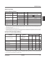
1
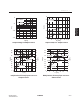
MF302-10
L
A
NU
L
C
TE
H
A
NIC
MA
NOTICE
No part of this material may be reproduced or duplicated in any from or by any means without the
written permission of Seiko Epson. Seiko Epson reserves the right to make changes to this material
without notics. Seiko Epson does not assume any liability of any kind arising out of any inaccuracies
contained in this material or due to its application or use in any product or circuit and, further, there
is no repersesnation that this material is applicable to products requiring high level reliability, such as,
medical products. Moreover, no license to any intellectual property rights is granted by implication or
otherwise, and there is no representation or warranty that anything made in accordance with this
material will be free from any patent or copyright infringement of a third party. This material or
portions thereof may contain technology or the subject relating to strategic products under the control
of the Foreign Exchange and Foreign Trade Low of Japan and may require an export licenes from the
Ministry of International Trade and Industry or other approval from another government agency.
HD44103 is a registered trademark of Hitachi, Ltd.
All other product names mentioned herein are trademarks and/or registered trademarks of their
respective companies.
©Seiko Epson Corporation 1999 All rights reserved.
al
u
an
lM
c
Te
h
a
nic
Contents
Introduction .......................................................................................................................................................................... 1
Selection Guide .................................................................................................................................................................... 2
1. DC/DC Converter
SCI7660 Series
DESCRIPTION .......................................................................................................................................................... 1–1
FEATURES ............................................................................................................................................................... 1–1
APPLICATIONS ........................................................................................................................................................ 1–1
BLOCK DIAGRAM .................................................................................................................................................... 1–1
PIN CONFIGURATION ............................................................................................................................................. 1–1
PIN DESCRIPTION ................................................................................................................................................... 1–1
SPECIFICATIONS .................................................................................................................................................... 1–2
FUNCTIONAL DESCRIPTION .................................................................................................................................. 1–7
TYPICAL APPLICATIONS ........................................................................................................................................ 1–8
2. DC/DC Converter & Voltage Regulator
SCI7661 Series
DESCRIPTION .......................................................................................................................................................... 2–1
FEATURES ............................................................................................................................................................... 2–1
APPLICATIONS ........................................................................................................................................................ 2–1
BLOCK DIAGRAM .................................................................................................................................................... 2–1
PIN CONFIGURATION ............................................................................................................................................. 2–2
PIN DESCRIPTION ................................................................................................................................................... 2–2
SPECIFICATIONS .................................................................................................................................................... 2–3
FUNCTIONAL DESCRIPTION ................................................................................................................................ 2–11
TYPICAL APPLICATIONS ...................................................................................................................................... 2–12
SCI7654 Series
DESCRIPTION ........................................................................................................................................................ 2–15
FEATURES ............................................................................................................................................................. 2–15
APPLICATIONS ...................................................................................................................................................... 2–15
BLOCK DIAGRAM .................................................................................................................................................. 2–16
PIN DESCRIPTION ................................................................................................................................................. 2–16
ELECTRICAL CHARACTERISTICS ....................................................................................................................... 2–19
EXPLANATION OF FUNCTIONS ........................................................................................................................... 2–22
CHARACTERISTICS GRAPHICS .......................................................................................................................... 2–29
APPLICATION CIRCUIT EXAMPLES .................................................................................................................... 2–30
SCI7000 Series
Technical Manual
EPSON
i
Contents
3. Voltage Regulator
SCI7810Y Series
DESCRIPTION .......................................................................................................................................................... 3–1
FEATURES ............................................................................................................................................................... 3–1
BLOCK DIAGRAM .................................................................................................................................................... 3–1
MODEL CLASSIFICATION ....................................................................................................................................... 3–2
PIN DESCRIPTION ................................................................................................................................................... 3–2
DESCRIPTION OF FUNCTION ................................................................................................................................ 3–3
ABSOLUTE MAXIMUM RATING .............................................................................................................................. 3–4
ELECTRIC CHARACTERISTICS ............................................................................................................................. 3–5
EXAMPLES OF APPLIED CIRCUITS ..................................................................................................................... 3–12
SCI7910Y Series
DESCRIPTION ........................................................................................................................................................ 3–14
FEATURES ............................................................................................................................................................. 3–14
APPLICATIONS ...................................................................................................................................................... 3–14
LINE-UP .................................................................................................................................................................. 3–14
BLOCK DIAGRAM .................................................................................................................................................. 3–14
PIN CONFIGURATION ........................................................................................................................................... 3–14
PIN DESCRIPTION ................................................................................................................................................. 3–15
SPECIFICATIONS .................................................................................................................................................. 3–15
PACKAGE MARKINGS ........................................................................................................................................... 3–28
FUNCTIONAL DESCRIPTION ................................................................................................................................ 3–28
TYPICAL APPLICATIONS ...................................................................................................................................... 3–29
4. DC/DC Switching Regulators
SCI7630 Series
SCI7631, SCI7638 Series
DESCRIPTION ................................................................................................................................................ 4–1
FEATURES ..................................................................................................................................................... 4–1
APPLICATIONS .............................................................................................................................................. 4–1
LINE-UP .......................................................................................................................................................... 4–1
BLOCK DIAGRAMS ........................................................................................................................................ 4–2
PIN CONFIGURATIONS ................................................................................................................................. 4–3
PIN DESCRIPTIONS ....................................................................................................................................... 4–3
SPECIFICATIONS ........................................................................................................................................... 4–4
PACKAGE MARKINGS ................................................................................................................................. 4–13
FUNCTIONAL DESCRIPTION ...................................................................................................................... 4–13
ii
EPSON
SCI7000 Series
Technical Manual
Contents
TYPICAL APPLICATIONS ............................................................................................................................ 4–15
SCI7633 Series
DESCRIPTION .............................................................................................................................................. 4–21
FEATURES ................................................................................................................................................... 4–21
APPLICATIONS ............................................................................................................................................ 4–21
LINE-UP ........................................................................................................................................................ 4–22
BLOCK DIAGRAMS ...................................................................................................................................... 4–22
PIN CONFIGURATIONS ............................................................................................................................... 4–22
PIN DESCRIPTIONS ..................................................................................................................................... 4–22
SPECIFICATIONS ......................................................................................................................................... 4–23
PACKAGE MARKINGS ................................................................................................................................. 4–25
FUNCTIONAL DESCRIPTION ...................................................................................................................... 4–26
TYPICAL APPLICATIONS ............................................................................................................................ 4–27
5. Voltage Detector
SCI7720Y Series
DESCRIPTION .......................................................................................................................................................... 5–1
FEATURES ............................................................................................................................................................... 5–1
MODEL GROUPS ..................................................................................................................................................... 5–2
BLOCK DIAGRAM .................................................................................................................................................... 5–3
PIN DESCRIPTION ................................................................................................................................................... 5–4
DESCRIPTION OF FUNCTION ................................................................................................................................ 5–4
ABSOLUTE MAXIMUM RATINGS ............................................................................................................................ 5–5
ELECTRIC CHARACTERISTICS ............................................................................................................................. 5–6
EXAMPLES OF EXTERNAL CONNECTION .......................................................................................................... 5–19
SAMPLE CIRCUITS (SCI7721Y SERIES) .............................................................................................................. 5–20
SAMPLE CIRCUITS (SCI7720Y SERIES) .............................................................................................................. 5–21
PRECAUTIONS ...................................................................................................................................................... 5–22
6. Appendix
ORDERING INFORMATION ..................................................................................................................................... 6–1
CMOS LSI LINEUP ................................................................................................................................................... 6–2
ABSOLUTE MAXIMUM RATINGS ............................................................................................................................ 6–3
RECOMMENDER OPERATING CONDITIONS ....................................................................................................... 6–3
ELECTRICAL CHARACTERISTICS ......................................................................................................................... 6–3
POWER DISSIPATION CONDITIONS ..................................................................................................................... 6–3
PARAMETER SUMMARY ........................................................................................................................................ 6–4
SCI7000 Series
Technical Manual
EPSON
iii
Contents
DIMENSIONS ........................................................................................................................................................... 6–6
EMBOSS CARRIER TAPING STANDARD (3-PIN SOT89)
TAPING INFORMATION ........................................................................................................................................... 6–8
REEL SPECIFICATIONS .......................................................................................................................................... 6–9
DEVICE POSITIONING ............................................................................................................................................ 6–9
EMBOSS CARRIER TAPING STANDARD (8-PIN SOP3)
TAPING INFORMATION ......................................................................................................................................... 6–10
REEL SPECIFICATIONS ........................................................................................................................................ 6–11
DEVICE POSITIONING .......................................................................................................................................... 6–11
EMBOSS CARRIER TAPING STANDARD (14-PIN SOP5)
TAPING INFORMATION ......................................................................................................................................... 6–13
REEL SPECIFICATIONS ........................................................................................................................................ 6–14
DEVICE POSITIONING .......................................................................................................................................... 6–14
EMBOSS CARRIER TAPING STANDARD (24-PIN SOP2)
TAPING INFORMATION ......................................................................................................................................... 6–16
REEL SPECIFICATIONS ........................................................................................................................................ 6–18
DEVICE POSITIONING .......................................................................................................................................... 6–18
iv
EPSON
SCI7000 Series
Technical Manual
Introduction
This book describes SEIKO EPSON's full line of power
supply ICs and includes a complete set of product
specifications. Also included are sections on quality
assurance and packaging.
We suggest that you use the selector guide beginning
on the following page to choose the IC or IC series that
most closely matches your application. You can then
SCI7000 Series
Technical Manual
use the detailed product descriptions in subsequent
sections to confirm device specifications and characteristics.
Please contact your local SEIKO EPSON sales
representative for further information or assistance on
these or other products.
EPSON
1
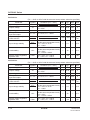
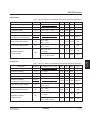
Selection Guide
DC/DC Converter
Part number
SCI7660C0B
SCI7660M0B
Features
• Supply voltage conversion IC.
• It effectively converts input voltage into two levels in positive potential or
negative potential (millipedes by 1 the in reverse polarity and doubles in the
same polarity).
• Power conversion efficiency: 95%, as standard.
Package
DIP-8pin
SOP4-8pin
DC/DC Converter and Voltage Regulator
Part number
SCI7661C0B
SCI7661M0B/MBB
SCI7654C0A
SCI7654M0A
Features
• Supply voltage conversion IC.
• If effectively converts input voltage in for levels in positive potential or
negative potential (millipedes by 1 or doubles in the reverse polarity and
doubles or triples in the same polarity).
• Power conversion efficiency: 95%, as standard.
• It is capable of selecting temperature gradient for LCD power supply.
•
•
•
•
Supply voltage conversion IC.
It effectively converts input voltage in for levels in negative potential.
Power conversion efficiency: 95%, as standard.
It is capable of selecting temperature gradient for LCD power supply.
Package
DIP-14pin
SOP5-14pin
SSOP2-16pin
DIP-16pin
SSOP2-16pin
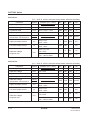
Voltage regulator
Part number
2
Features
Package
SCI7810YAA
• 6.00V positive output voltage regulator.
• Low operating current (typ 1.5 uA).
• Input voltage stability (typ 0.1%/V).
SOT89-3pin
SCI7810YBA
• 5.00V positive output voltage regulator.
• Low operating current (typ 1.5 uA).
• Input voltage stability (typ 0.1%/V).
SOT89-3pin
SCI7810YMA
• 4.50V positive output voltage regulator.
• Low operating current (typ 1.5 uA).
• Input voltage stability (typ 0.1%/V).
SOT89-3pin
SCI7810YPA
• 4.00V positive output voltage regulator.
• Low operating current (typ 1.5 uA).
• Input voltage stability (typ 0.1%/V).
SOT89-3pin
SCI7810YKA
• 3.90V positive output voltage regulator.
• Low operating current (typ 1.5 uA).
• Input voltage stability (typ 0.1%/V).
SOT89-3pin
SCI7810YNA
• 3.50V positive output voltage regulator.
• Low operating current (typ 1.5 uA).
• Input voltage stability (typ 0.1%/V).
SOT89-3pin
SCI7810YTA
• 3.30V positive output voltage regulator.
• Low operating current (typ 1.5 uA).
• Input voltage stability (typ 0.1%/V).
SOT89-3pin
SCI7810YCA
• 3.20V positive output voltage regulator.
• Low operating current (typ 1.5 uA).
• Input voltage stability (typ 0.1%/V).
SOT89-3pin
SCI7810YDA
• 3.00V positive output voltage regulator.
• Low operating current (typ 1.5 uA).
• Input voltage stability (typ 0.1%/V).
SOT89-3pin
SCI7810YRA
• 2.80V positive output voltage regulator.
• Low operating current (typ 1.5 uA).
• Input voltage stability (typ 0.1%/V).
SOT89-3pin
SCI7810YLA
• 2.60V positive output voltage regulator.
• Low operating current (typ 1.5 uA).
• Input voltage stability (typ 0.1%/V).
SOT89-3pin
EPSON
SCI7000 Series
Technical Manual
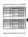
Selection Guide
Part number
Features
Package
SCI7810YFA
• 2.20V positive output voltage regulator.
• Low operating current (typ 1.5 uA).
• Input voltage stability (typ 0.1%/V).
SOT89-3pin
SCI7810YGA
• 1.80V positive output voltage regulator.
• Low operating current (typ 1.5 uA).
• Input voltage stability (typ 0.1%/V).
SOT89-3pin
SCI7810YHA
• 1.50V positive output voltage regulator.
• Low operating current (typ 1.5 uA).
• Input voltage stability (typ 0.1%/V).
SOT89-3pin
SCI7910YBA
• –5.00V negative output voltage regulator.
• Low operating current (typ 1.5 uA).
• Input voltage stability (typ 0.1%/V).
SOT89-3pin
SCI7910YPA
• –4.00V negative output voltage regulator.
• Low operating current (typ 1.5 uA).
• Input voltage stability (typ 0.1%/V).
SOT89-3pin
SCI7910YDA
• –3.00V negative output voltage regulator.
• Low operating current (typ 1.5 uA).
• Input voltage stability (typ 0.1%/V).
SOT89-3pin
SCI7910YGA
• –1.80V negative output voltage regulator.
• Low operating current (typ 1.5 uA).
• Input voltage stability (typ 0.1%/V).
SOT89-3pin
DC/DC Switching regulator
Part number
Features
Package
SCI7631MHA
•
•
•
•
•
•
Step-up switching regulator (from 1.5V to 2.2V).
Low operating voltage (0.9V at minimum).
Low operating current
High precision voltage detection function and battery backup function.
Built-in CR oscillator circuit.
Power-on clear function.
SOP3-8pin
SCI7631MLA
•
•
•
•
•
•
Step-up switching regulator (from 1.5V to 2.4V).
Low operating voltage (0.9V at minimum).
Low operating current
High precision voltage detection function and battery backup function.
Built-in CR oscillator circuit.
Power-on clear function.
SOP3-8pin
SCI7631MBA
•
•
•
•
•
•
Step-up switching regulator (from 1.5V to 3.0V).
Low operating voltage (0.9V at minimum).
Low operating current
High precision voltage detection function and battery backup function.
Built-in CR oscillator circuit.
Power-on clear function.
SOP3-8pin
SCI7631MKA
•
•
•
•
•
•
Step-up switching regulator (from 1.5V to 3.5V).
Low operating voltage (0.9V at minimum).
Low operating current
High precision voltage detection function and battery backup function.
Built-in CR oscillator circuit.
Power-on clear function.
SOP3-8pin
SCI7631MAA
•
•
•
•
•
•
Step-up switching regulator (from 1.5V to 5.0V).
Low operating voltage (0.9V at minimum).
Low operating current
High precision voltage detection function and battery backup function.
Built-in CR oscillator circuit.
Power-on clear function.
SOP3-8pin
SCI7000 Series
Technical Manual
EPSON
3
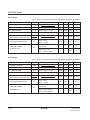
Selection Guide
Part number
Features
Package
SCI7638MHA
•
•
•
•
•
•
•
Step-up switching regulator (from 1.5V to 2.2V).
Low operating voltage (0.9V at minimum).
Low operating current.
Built-in CR oscillator circuit.
High precision voltage detection.
Output voltage response compensation.
Temperature characteristics of output voltage for LCD panel (-4.5mV/C).
SOP3-8pin
SCI7638MLA
•
•
•
•
•
•
•
Step-up switching regulator (from 1.5V to 2.4V).
Low operating voltage (0.9V at minimum).
Low operating current.
Built-in CR oscillator circuit.
High precision voltage detection.
Output voltage response compensation.
Temperature characteristics of output voltage for LCD panel (-4.0mV/C).
SOP3-8pin
SCI7633MBA
•
•
•
•
•
Step-up switching regulator (from 1.5V to 3.0V).
Low operating voltage (0.9V at minimum).
Low operating current.
Built-in crystal oscillator circuit.
Equipped with crystal oscillator output pin.
SOP3-8pin
Voltage detector
Part number
4
Features
Package
SCI7720YTA
• Voltage detection (Typ 4.00V).
• Output format: N-ch open drain.
• Low operating power (Typ 2.0 uA, VDD = 5.0V).
SOP89-3pin
SCI7720YFA
• Voltage detection (Typ 2.65V).
• Output format: N-ch open drain.
• Low operating power (Typ 2.0 uA, VDD = 3.0V).
SOP89-3pin
SCI7720YCA
• Voltage detection (Typ 2.15V).
• Output format: N-ch open drain.
• Low operating power (Typ 2.0 uA, VDD = 3.0V).
SOP89-3pin
SCI7720YNA
• Voltage detection (Typ 1.90V).
• Output format: N-ch open drain.
• Low operating power (Typ 2.0 uA, VDD = 3.0V).
SOP89-3pin
SCI7720YBA
• Voltage detection (Typ 1.15V).
• Output format: N-ch open drain.
• Low operating power (Typ 1.5 uA, VDD = 1.5V).
SOP89-3pin
SCI7720YYA
• Voltage detection (Typ 1.10V).
• Output format: N-ch open drain.
• Low operating power (Typ 1.5 uA, VDD = 1.5V).
SOP89-3pin
SCI7720YAA
• Voltage detection (Typ 1.05V).
• Output format: N-ch open drain.
• Low operating power (Typ 1.5 uA, VDD = 1.5V).
SOP89-3pin
SCI7720YVA
• Voltage detection (Typ 0.95V).
• Output format: N-ch open drain.
• Low operating power (Typ 1.5 uA, VDD = 1.5V).
SOP89-3pin
SCI7721YLA
• Voltage detection (Typ 5.00V).
• Output format: COMS.
• Low operating power (Typ 2.0 uA. VDD = 6.0V).
SOP89-3pin
SCI7721YKA
• Voltage detection (Typ 4.80V).
• Output format: COMS.
• Low operating power (Typ 2.0 uA. VDD = 5.0V).
SOP89-3pin
EPSON
SCI7000 Series
Technical Manual
Selection Guide
Part number
Features
Package
SCI7721Y2A
• Voltage detection (Typ 4.60V).
• Output format: COMS.
• Low operating power (Typ 2.0 uA. VDD = 5.0V).
SOP89-3pin
SCI7721YJA
• Voltage detection (Typ 4.40V).
• Output format: COMS.
• Low operating power (Typ 2.0 uA. VDD = 5.0V).
SOP89-3pin
SCI7721YMA
• Voltage detection (Typ 4.20V).
• Output format: COMS.
• Low operating power (Typ 2.0 uA. VDD = 5.0V).
SOP89-3pin
SCI7721YTA
• Voltage detection (Typ 4.00V).
• Output format: COMS.
• Low operating power (Typ 2.0 uA. VDD = 5.0V).
SOP89-3pin
SCI7721Y3A
• Voltage detection (Typ 3.50V).
• Output format: COMS.
• Low operating power (Typ 2.0 uA. VDD = 4.0V).
SOP89-3pin
SCI7721YHA
• Voltage detection (Typ 3.20V).
• Output format: COMS.
• Low operating power (Typ 2.0 uA. VDD = 4.0V).
SOP89-3pin
SCI7721YGA
• Voltage detection (Typ 3.00V).
• Output format: COMS.
• Low operating power (Typ 2.0 uA. VDD = 4.0V).
SOP89-3pin
SCI7721YRA
• Voltage detection (Typ 2.80V).
• Output format: COMS.
• Low operating power (Typ 2.0 uA. VDD = 3.0V).
SOP89-3pin
SCI7721YFA
• Voltage detection (Typ 2.65V).
• Output format: COMS.
• Low operating power (Typ 2.0 uA. VDD = 3.0V).
SOP89-3pin
SCI7721YEA
• Voltage detection (Typ 2.55V).
• Output format: COMS.
• Low operating power (Typ 2.0 uA. VDD = 3.0V).
SOP89-3pin
SCI7721YSA
• Voltage detection (Typ 2.35V).
• Output format: COMS.
• Low operating power (Typ 2.0 uA. VDD = 3.0V).
SOP89-3pin
SCI7721YPA
• Voltage detection (Typ 2.25V).
• Output format: COMS.
• Low operating power (Typ 2.0 uA. VDD = 3.0V).
SOP89-3pin
SCI7721YCA
• Voltage detection (Typ 2.15V).
• Output format: COMS.
• Low operating power (Typ 2.0 uA. VDD = 3.0V).
SOP89-3pin
SCI7721YFB
• Voltage detection (Typ 2.65V).
• Output format: COMS.
• Low operating power (Typ 2.0 uA. VDD = 3.0V).
SOP89-3pin
SCI7721YCB
• Voltage detection (Typ 2.15V).
• Output format: COMS.
• Low operating power (Typ 2.0 uA. VDD = 3.0V).
SOP89-3pin
SCI7722YDB
• Voltage detection (Typ. 1.25V).
• Output format: P-ch open drain.
• Low operating power (Typ 1.5 uA. VDD = 1.5V).
SOP89-3pin
SCI7000 Series
Technical Manual
EPSON
5
er
n
rt
ve
C
D
C/
D
1.
Co
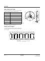
SCI7660 Series
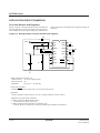
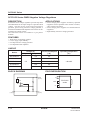
DESCRIPTION
DC/DC
Converter
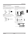
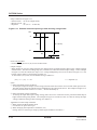
BLOCK DIAGRAM
The SCI7660 Series is a highly efficient CMOS DC/DC
converter for doubling an input voltage. This powersaving IC allows portable computers and similar handheld equipment to operate from a single power supply,
even when they incorporate LSIs that operate at voltages different from those of logic circuits, for example,
LCD drivers and analog LSIs.
The SCI7660C0B is available in 8-pin plastic DIPs, and
the SCI7660M0B, in 8-pin plastic SOPs.
VDD
OSC1
RC oscillator
OSC2
VI
FEATURES
CAP1+
CAP1–
Voltage converter
•
•
•
•
95% (typ.) conversion efficiency
Two output voltages, VO, relative to VDD and VI
30mA maximum output current at 5V
Two-in-series configuration doubles negative output
voltage.
• Low operating voltage
• On-chip RC oscillator
• 8-pin plastic DIP and 8-pin plastic SOP
VO
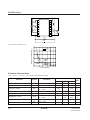
PIN CONFIGURATION
8 VI
NC 1
APPLICATIONS
• Fixed-voltage power supplies for battery-operated
equipment
• Power supplies for pagers, memory cards, calculators
and similar hand-held equipment
• Fixed-voltage power supplies for medical equipment
• Fixed-voltage power supplies for communications
equipment
• Uninterruptable power supplies
7 VO
OSC2 2
SCI7660C0B
OSC1 3
6 CAP1–
VDD 4
5 CAP1+
PIN DESCRIPTION
Number
Name
1
NC
2
OSC2
Resistor connection. Open when using external clock
3
OSC1
Resistor connection. Clock input when using external clock
4
VDD
5
CAP1+
Positive charge-pump connection
6
CAP1–
Negative charge-pump connection
7
VO
×2 multiplier output
8
VI
Negative supply (system ground)
SCI7000 Series
Technical Manual
Description
No connection
Positive supply (system VCC)
EPSON
1–1
SCI7660 Series
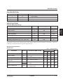
SPECIFICATIONS
Absolute Maximum Ratings
Parameter
Symbol
Rating
Unit
Input voltage range
VI
–10.0 to 0.5
V
Output voltage range
VO
Min. –20.0
V
Power dissipation
PD
300 (DIP)
mW
150 (SOP)
Operating temperature range
Topr
–40 to 85
˚C
Storage temperature range
Tstg
–65 to 150
˚C
Soldering temperature(for 10s). See note.
Tsol
260
˚C
Note:
Temperatures during reflow soldering must remain within the limits set out in LSI Device Precautions.
Never use solder dip to mount SCI7000 series power supply devices.
Recommended Operating Conditions
VDD = 0V, Ta = –40 to 85˚C unless otherwise noted
Parameter
Oscillator startup voltage
Oscillator shutdown voltage
Symbol
VSTA
VSTP
Condition
ROSC = 1MΩ,
C1/C2≤1/20, C2≥10µF,
Ta = –40 to 85˚C
See note 1.
Rating
Min.
Typ.
Max.
—
—
–1.5
Unit
V
ROSC = 1MΩ
—
—
–2.2
ROSC = 1MΩ
–1.5
—
—
V
Load resistance
RL
RL min
See note 2.
—
—
Ω
Output current
IO
—
—
30.0
mA
Clock frequency
fOSC
10.0
—
30.0
kHz
RC oscillator network
resistance
ROSC
680
—
2,000
kΩ
Capacitance
C1, C2
3.3
—
—
µF
Notes:
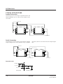
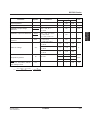
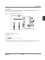
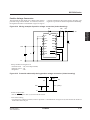
1. The recommended circuit configuration for low-voltage operation (when V I is between –1.2V and
–2.2V) is shown in the following figure. Note that diode D1 should have a maximum forward voltage of
0.6V with 1.0mA forward current.
2. RL min can be varied depending on the input voltage.
1–2
EPSON
SCI7000 Series
Technical Manual
SCI7660 Series
CL
1
8
2
7
3
6
4
5
+
C2
22µF
RL
DC/DC
Converter
Battery
D1
1MΩ
+
C1
10µF
3. RL min is a function of VI.
Minimum load resistance (kΩ)
5
4
VSTA1
3
2
1
0
1.0
VSTA2
1.5
3.0
2.0
Input voltage (V)
4.0
5.0 6.0
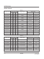
Electrical Characteristics
VDD = 0V, Ta = –40 to 85˚C unless otherwise noted
Parameter
Symbol
Condition
Rating
Min.
Typ.
Max.
Unit
Input voltage
VI
–8.0
—
–1.5
V
Output voltage
VO
–16.0
—
—
V
Multiplier current
Iopr
RL = ∞, ROSC = 1MΩ
VI = –5V
—
20
30
µA
Quiescent current
IQ
RL =∞, VI = –8V
—
—
2.0
µA
fOSC
ROSC = 1MΩ, VI = –5V
16
20
24
kHz
Output impedance
RO
IO = 10mA, VI = –5V
—
75
100
Ω
Multiplication efficiency
Peff
IO = 5mA, VI = –5V
90
95
—
%
OSC1 Input leakage current
ILKI
VI = –8V
—
—
2.0
µA
Clock frequency
SCI7000 Series
Technical Manual
EPSON
1–3
SCI7660 Series
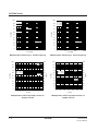
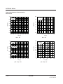
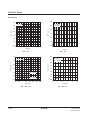
Typical Performance Characteristics
1000
Ta = 25°C
VI = –5V
VI = –3V
VI = –2V
fOSC [KHz]
fOSC [KHz]
100
10
1
10
100
1000
26
25
24
23
22
21
20
19
18
17
16
15
14
13
12
11
10
9
8
VI = –5.0V
VI = –3.0V
VI = –2.0V
–40
10000
–20
0
ROSC [kΩ]
Clock frequency vs. External resistance
20
40
Ta [°C]
60
80
100
Clock frequency vs. Ambient temperature
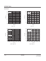
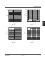
50
0
fOSC = 40kHz
45
Ta = 25
VI = –5.0V
40
Ta = 25°C
fOSC =
20kHz
30
25
20
–5
VO [V]
@lopr[µA]
35
fOSC =
10kHz
–10
15
10
5
–15
0
–7
–6
–5
–4
–3
VI [V]
–2
–1
0
Multiplier current vs. Input voltage
1–4
0
10
20
30
IO [mA]
40
50
Output voltage vs. Output current
EPSON
SCI7000 Series
Technical Manual
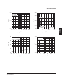
SCI7660 Series
0
0
Ta = 25°C
VI = –2.0V
–1
DC/DC
Converter
Ta = 25°C
VI = –3.0V
VO [V]
VO [V]
–2
–5
–3
–4
–5
–6
–10
0
10
20
0
30
1
2
3
IO [mA]
Output voltage vs. Output current
4
5 6
IO [mA]
7
8
9
10
Output voltage vs. Output current
300
300
Ta = 25°C
IO = 7mA
Ta = 25°C
Io = 10mA
RO [Ω]
200
RO [Ω]
200
100
100
0
0
–7
–6
–5
–4
–3
–2
–1
0
VI [V]
–6
–5
–4
–3
–2
–1
0
VI [V]
Output impedance vs. Input voltage
SCI7000 Series
Technical Manual
–7
Output impedance vs. Input voltage
EPSON
1–5
SCI7660 Series
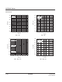
100
90
80
IO = 30mA
70
70
IO = 20mA
Peff [%]
60
IO = 0.5mA
IO = 1.0mA
IO = 2.0mA
IO = 4.0mA
90
IO = 10mA
80
Peff [%]
100
IO = 2mA
IO = 5mA
50
40
60
50
40
30
30
VI = –5.0V
20
20
10
10
0
VI = –3.0V
0
1
10
100
1000
1
10
fOSC [kHz]
100
1000
fOSC [kHz]
Multiplication efficiency vs. Clock frequency
100
Multiplication efficiency vs. Clock frequency
100
100
100
90
90
90
90
80
80
80
II
50
70
60
60
50
60
50
50
40
40
40
40
30
30
30
30
20
20
20
20
10
10
10
10
0
10
20
30
40
Peff
0
0
0
0
0
50
IO [mA]
5
10
15
20
25
30
IO [mA]
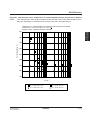
Multiplication efficiency/input current vs.
Output current
1–6
70
Ta = 25°C
VI = –3.0V
II [mA]
Peff [%]
Peff
70
Peff [%]
Ta = 25°C
VI = –5.0V
60
II [mA]
70
80
II
Multiplication efficiency/input current vs.
Output current
EPSON
SCI7000 Series
Technical Manual
SCI7660 Series
100
40
90
36
Peff
32
70
28
Ta = 25°C
VI = –2.0V
24
50
20
II
40
16
30
12
20
8
10
4
0
II [mA]
60
Peff [%]
DC/DC
Converter
80
0
0
1
2
3
4
5
6
7
8
9
10
IO [mA]
Multiplication efficiency/input current vs.
Output current
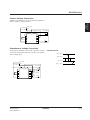
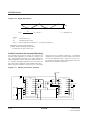
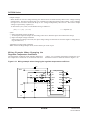
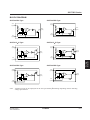
FUNCTIONAL DESCRIPTION
RC Oscillator
Voltage Multiplier
The on-chip RC oscillator network frequency is determined by the external resistor, ROSC, connected between OSC1 and OSC2. This oscillator can be disabled
in favor of an external clock by leaving OSC2 open and
applying an external clock signal to OSC1.
The voltage multiplier uses the clock signal from the
oscillator to double the input voltage. This requires two
external capacitors—a charge-pump capacitor, C1, between CAP1+ and CAP1–, and a smoothing capacitor,
C2, between VI and VO.
Oscillator
External clock
VDD = 0 V
5V
External clock
signal
ROSC
OSC2
VI = –5 V
OSC1
OSC1
OSC2
1
8
2
7
3
6
4
5
+
C2
10µF
VO1 = –10V (2VI)
1MΩ
+
C1
10µF
Doubled potential levels
SCI7000 Series
Technical Manual
EPSON
VCC
(+5V)
VDD = 0 V
GND
VI = –5 V
(–5V)
VO = (2VI) = –10 V
1–7
SCI7660 Series
TYPICAL APPLICATIONS
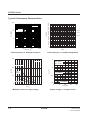
Parallel Connection
Connecting two or more chips in parallel reduces the
output impedance by 1/n, where n is the number of devices used.
VDD = 0 V
5V
VI = –5 V
1
8
2
7
3
6
+
C2
10µF
1
8
2
7
3
6
4
5
1MΩ
1MΩ
5
4
C1
10µF
+
C1
10µF
+
VO = –10 V
Serial Connection
Connecting two or more chips in series obtains a higher
output voltage than can be obtained using a parallel
connection, however, this also raises the output impedance.
VDD = 0 V
VI = –5 V
5V
VDD' = VI = –5
1
8
2
7
3
6
4
5
+
C2
10µF
1
8
2
7
3
6
4
5
+
C2
10µF
1MΩ
1MΩ
+
C1
10µF
VO = –10 V = VI'
+
C1
10µF
VO' = –15 V
Potential levels
VDD (0 V)
VI (–5 V)
VO (–10 V)
VDD
VI
VO (–15 V)
Primary stage
1–8
Secondary stage
EPSON
SCI7000 Series
Technical Manual
SCI7660 Series
Positive Voltage Conversion
DC/DC
Converter
Diodes can be added to a circuit connected in parallel to
make a negative voltage positive.
VDD = 0 V
VI = –5 V
5V
VO' = 3.8 V
C2
1
8
2
7
3
6
4
5
+
10µF
1MΩ
C1
+
10µF
Simultaneous Voltage Conversion
Combining a multiplier circuit with a positive voltage
conversion circuit generates both –10 and 3.8 V outputs
from a single input.
Potential levels
VO2 = 3.8 V
VDD = 0 V
VI= –5 V
VDD = 0 V
VI = –5 V
VO1 = –10 V
5V
VO2 = 3.8 V
C4
1
8
2
7
3
6
4
5
1MΩ
SCI7000 Series
Technical Manual
+ C2
10µF
+
10µF
VO1 = –10 V
C1
+ 10µF
C3
+
10µF
EPSON
1–9
2.
er
t
r
tor
ve
a
l
n
Co egu
DC ge R
/
DC olta
V
&
DESCRIPTION
APPLICATIONS
The SCI7661 Series is a highly effecient CMOS DC/
DC converter for doubling or tripling an input voltage.
It incorporates an on-chip voltage regulator to ensure
stable output at the specified voltage. The SCI7661 Series offers a choice of three, optional temperature gradients for applications such as LCD panel power supplies.
The SCI7661C0B is available in 14-pin plastic DIPs, the
SCI7661M 0B , in 14-pin plastic SOPs, and the
SCI7661MBB in 16-pin plastic SSOPs.
• Power supplies for LCD panels
• Fixed-voltage power supplies for battery-operated
equipment
• Power supplies for pagers, memory cards, calculators
and similar hand-held equipment
• Fixed-voltage power supplies for medical equipment
• Fixed-voltage power supplies for communications
equipment
• Power supplies for microcomputers
• Uninterruptable power supplies
FEATURES
• 95% (Typ.) conversion efficiency
• Up to four output voltages, VO, relative to the input
voltage, VI
• On-chip voltage regulator
• 20mA maximum output current at VI = –5V
• Three temperature gradients––0.1, 0.4 and 0.6%/°C
• External shut-down control
• 2µA maximum output current when shut-down
• Two-in-series configuration doubles negative output
voltage.
• On-chip RC oscillator
• SCI7661C0B ................ pladtic DIP-14 pin
SCI7661M0B ............... pladtic SOP5-14 Pin
SCI7661MBB .............. pladtic SSOP2-16 pin
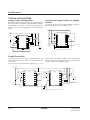
BLOCK DIAGRAM
VDD
OSC1
Oscilator
OSC2
Reference
voltge
generator
VI
CAP1–
CAP1+
Temperature
gradient
selector
Voltage
multiplier
(1)
TC2
POFF
CAP2–
CAP2+
TC1
Voltage
multiplier
(2)
Voltage regulator
RV
VREG
VO
Multiplication
stage
SCI7000 Series
Technical Manual
Stabilization
stage
EPSON
2–1
DC/DC Converter
& Voltage Regulator
SCI7661 Series
SCI7661 Series
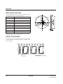
PIN CONFIGURATION
CAP+
1
14
CAP–
2
13
VDD
OSC1
CAP2+
3
12
OSC2
CAP2–
4
11
POFF
TC1
5
10
RV
TC2
6
9
VREG
VI 7
8
VO
CAP+
CAP–
NC
CAP2+
CAP2–
TC1
TC2
VI
SCI7661C0B/M0B
1
16
2
15
3
14
4
13
5
12
6
11
7
10
8
9
VDD
OSC1
NC
OSC2
POFF
RV
VREG
VO
SCI7661MBB
PIN DESCRIPTION
2–2
Number
Name
1
CAP1+
Positive charge-pump connection for ×2 multiplier
2
CAP1–
Negative charge-pump connection for ×2 multiplier
3
CAP2+
Positive charge-pump connection for ×3 multiplier
4
CAP2–
Negative charge-pump connection for ×3 multiplier or ×2 multiplier output
5
TC1
6
TC2
Description
Temperature gradient selects
7
VI
Negative supply (system ground)
8
VO
×3 multiplier output
9
VREG
10
RV
Voltage regulator output
Voltage regulator output adjust
11
POFF
Voltage regulator output ON/OFF control
12
OSC2
Resistor connection. Open when using external clock
13
OSC1
Resistor connection. Clock input when using external clock
14
VDD
Positive supply (system VCC)
EPSON
SCI7000 Series
Technical Manual
SCI7661 Series
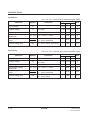
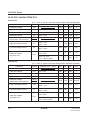
SPECIFICATIONS
Absolute Maximum Ratings
Input supply voltage
Input terminal voltage
Output voltage
Ratings
Codes
VI – VDD
VI – VDD
VO – VDD
Remarks
Units
N = 2: Boosting to a double voltage
–20/N to VDD + 0.3
V
VI – 0.3 to VDD + 0.3
V
VO – 0.3 to VDD + 0.3
V
TC1, TC2, RV
–20 to VDD + 0.3
V
VO
Note 3)
VO to VDD + 0.3
V
VREG
Note 3)
Allowable dissipation
Pd
Max. 300
mW
Working temperature
Topr
–40 to 85
°C
Storage temperature
Tstg
–55 to 150
°C
Soldering temperature
and time
Tsol
260°C
10 s (at leads)
N = 3: Boosting to a triple voltage
OSC1, OSC2, POFF
DC/DC Converter
& Voltage Regulator
Items
Plastic package
–
Notes
1. Using the IC under conditions exceeding the aforementioned absolute maximum ratings may lead to permanent destruction of
the IC. Also, if an IC is operated at the absolute maximum ratings for a longer period of time, its functional reliability may be
substantially deteriorated.
2. All the voltage ratings are based on VDD = 0V.
3. The output terminals (VO,VREG) are meant to output boosted voltage or stabilized boosted voltage. They, therefore, are not the
terminals to apply an external voltage. In case the using specifications unavoidably call for application of an external voltage,
keep such voltage below the voltage ratings given above.
Reconmmended Operating Conditions
VDD = 0V, Ta = –40 to 85˚C unless otherwise noted
Parameter
Symbol
Oscillator startup voltage
VSTA
Oscillator shutdown voltage
VSTP
Conditions
Rating
Unit
Min.
Typ.
Max.
–
–
–1.8
ROSC = 1MΩ
–
–
–2.2
ROSC = 1MΩ
–1.8
–
–
V
–
–
Ω
20.0
mA
ROSC =1MΩ
C3 = 10 µF, CL/C3 ≤ 1/20,
Ta = –40 to 85˚C.
See note 1.
V
Load resistance
RL
RL min.
See note 2.
Output current
IO
–
–
Clock frequency
fOSC
10.0
–
30.0
kHz
RC oscillator network resistance
ROSC
680
–
2,000
kΩ
C1, C2, C3
3.3
–
–
µF
RRV
100
–
1,000
kΩ
Capacitance
Stabilization voltage sensing resistance
Notes
1. The recommended circuit configuration for low-valtage operation (when VI is between –1.2V and –2.2V) is shown in
the following figure. Note that diode D1 should have a maximum forward voltage of 0.6V with 1.0mA forward current.
2. RL min can be varied depending on the input voltage.
SCI7000 Series
Technical Manual
EPSON
2–3
SCI7661 Series
C1
10µF
+
1
14
2
13
ROSC
1MΩ
C2 +
10µF
3
12
4
11
5
10
6
9
7
8
CL
RL
+C3
22µF
D1
3. RL min is a function of V1
Minimum load resistance (kΩ)
5
VSTA2
VSTA1
4
3
2
Voltage
tripler
1
Voltage
doubler
0
1
1.5
2
3
4
Input voltage (V)
5
6
Electrical Characteristics
VDD = 0V, V1 = –5V, Ta = –40 to 85°C unless otherwise noted
Parameter
Symbol
Conditions
Rating
Min.
Typ.
Max.
Unit
Input voltage
VI
–6.0
–
–1.8
V
Output voltage
VO
–18.0
–
–
V
–18.0
–
–2.6
V
–18.0
–
–3.2
V
–
40
80
µA
–
5.0
12.0
µA
Regulator voltage
Stabilization circuit operating voltage
VREG
VO
Multiplier current
Iopr1
Stabilization current
Iopr2
Quiescent current
Clock frequency
2–4
RL = ∞, RRV = 1MΩ,
VO = –18V
IQ
fOSC
RL = ∞, ROSC = 1MΩ
RL = ∞, RRV = 1MΩ,
VO = –15V
TC2 = TC1 = VO, RL = ∞
ROSC = 1MΩ
EPSON
–
–
2.0
µA
16.0
20.0
24.0
kHz
SCI7000 Series
Technical Manual
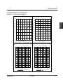
SCI7661 Series
Rating
Symbol
Conditions
Typ.
Max.
–
150
200
Ω
90.0
95.0
–
%
–
0.2
–
%/V
–
5.0
–
Ω
–
8.0
–
Ω
–2.3
–1.5
–1.0
TC2 = TC1 = VO,
Ta = 25˚C
–1.7
–1.3
–1.1
TC2 = VDD, TC1 = VO,
Ta = 25˚C
–1.1
–0.9
–0.8
–0.25
–0.1
–0.01
–0.5
–0.4
–0.3
–0.7
–0.6
–0.5
–
–
2.0
Output impedance
RO
IO = 10mA
Multiplication efficiency
Peff
IO = 5mA
Stabilization output voltage
differential
Stabilization output load differential
Stabilization output saturation
resistance
Reference voltage
Temperature gradient
POFF, TC1, TC2, OSC1, and RV
input leakage current
∆VREG
∆VO·VREG
∆VREG
∆IO
RSAT
VRV
CT
Unit
Min.
VO = –18 to –8V,
VREG = –8V, RL = ∞,
Ta = 25˚C
VO = –15V,
VREG = –8V, Ta = 25˚C,
IO = 0 to 10µA,
TC1 = VDD, TC2 = VO
RSAT = ∆(VREG – VO)/∆IO,
IO = 0 to 10µA,
RV = VDD, Ta = 25˚C
RC2 = VO, TC1 = VDD,
Ta = 25˚C
See note.
ILKI
V
%/˚C
µA
Note
CT =
|VREG (50°C)| – |VREG (0°C)|
100
×
50°C – 0°C
|VREG (25°C)|
SCI7000 Series
Technical Manual
EPSON
2–5
DC/DC Converter
& Voltage Regulator
Parameter
SCI7661 Series
Typical Performance Characteristics
1000
26
25
24
23
22
21
20
19
18
17
16
15
14
13
12
11
10
9
8
–40
Ta = 25°C
VI = –5V
VI = –3V
VI = –2V
fOSC [KHz]
fOSC [kHz]
100
10
1
10
100
1000
10000
VI = –5.0V
VI = –3.0V
VI = –2.0V
–20
ROSC [kΩ]
Clock frequency vs. External resistance
0
20
40
Ta [°C]
60
80
100
Clock frequency vs. Ambient temperature
150
0
Ta = 25°C
Ta = 25°C
VI = –5.0V
fOSC = 40kHz
100
VO [V]
Iopr [µA]
–5
fOSC =
20kHz
×2 multiplier
–10
50
×3 multiplier
fOSC = 10kHz
–15
0
–7
–6
–5
–4
–3
VI [V]
–2
–1
0
0
Multiplier current vs. Input voltage
2–6
10
20
IO [mA]
30
40
Output voltage vs. Output current
EPSON
SCI7000 Series
Technical Manual
SCI7661 Series
0
0
Ta = 25°C
VI = –3.0V
×2 multiplier
–2
×3 multiplier
–10
–3
×2 multiplier
–4
×3 multiplier
–5
–15
10
20
–6
30
0
IO [mA]
Output voltage vs. Output current
1
2
3
4
5 6
IO [mA]
7
8
9 10
Output voltage vs. Output current
100
100
100
60
90
90
90
54
80
80
80
×3 multiplier
II
50
40
70
70
×2 multiplier 60
Peff
50
×3 multiplier
Peff
40
60
Peff [%]
60
II [mA]
Ta = 25°C
VI = –5.0V
70
50
30
20
20
10
10
10
0
0
0
×2 multiplier
II
20
0
10
20
30
IO [mA]
40
24
12
×2 multiplier
II
6
0
5
10
15
20
25
30
IO [mA]
Multiplication efficiency/input current vs.
Output current
SCI7000 Series
Technical Manual
30
×3 multiplier
Peff
18
0
50
×2 multiplier 42
Peff
36
×3 multiplier
II
40
30
30
48
Ta = 25°C
VI = –3.0V
II [mA]
0
Peff [%]
DC/DC Converter
& Voltage Regulator
VO [V]
Vo [V]
–5
Ta = 25°C
VI = –2.0V
–1
Multiplication efficiency/input current vs.
Output current
EPSON
2–7
SCI7661 Series
500
40
100
×2 multiplier
Peff
90
400
32
80
×3 multiplier
Peff
24
20
50
×3 multiplier
II
40
Rout [Ω]
60
28
II [mA]
Ta = 25°C
VI = –2.0V
70
Peff [%]
Ta = 25°C
IO = 6mA
36
300
200
16
×3 multiplier
12
30
×2 multiplier
II
20
×2 multiplier
100
8
4
10
0
0
0
0
1
2
3
4
5 6
IO [mA]
7
8
9
–7
10
–6
–5
–4
–3
–2
–1
0
VI [V]
Multiplication efficiency/input current vs.
Output current
Output impedance vs. Input voltage
500
100
Ta = 25°C
IO = 10mA
400
IO = 2mA
90
Peff [%]
Rout [Ω]
IO = 5mA
300
200
80
IO = 10mA
70
×3 multiplier
IO = 20mA
×2 multiplier
100
60
IO = 30mA
0
50
–7
–6
–5
–4
–3
–2
–1
0
1
Output impedance vs. Input voltage
10
100
1000
fOSC [kHz]
VI [V]
2–8
Ta = 25°C
VI = –5.0V
Multiplication efficiency vs. Clock frequency
EPSON
SCI7000 Series
Technical Manual
SCI7661 Series
100
–7.850
IO = 0.5mA
IO = 1.0mA
90
VO = –15V
IO = 2.0mA
Ta = 25°C
–7.900
80
DC/DC Converter
& Voltage Regulator
VREG [V]
Peff [%]
IO = 4.0mA
70
–7.950
Ta = 25°C
60
VI = – 3.0V
–8.000
0.0001
50
1
10
100
1000
0.0010
0.0100
0.1000
IO [V]
fOSC [kHz]
Multiplication efficiency vs. Clock frequency
Output voltage vs. Output current
–2.850
–5.850
VO = –6V
VO = –9V
Ta = 25°C
Ta = 25°C
–5.900
VREG [V]
VREG [V]
–2.900
–2.950
–5.950
–6.000
0.0001
–3.000
0.0010
0.0100
0.1000
IO [V]
0.0010
0.0100
0.1000
IO [V]
Output voltage vs. Output current
SCI7000 Series
Technical Manual
0.0001
Output voltage vs. Output current
EPSON
2–9
SCI7661 Series
0.30
0.25
VO = –5V
|VREG-VO| [V]
0.20
VO = –10V
VO = –15V
0.15
0.10
0.05
100×|VREG(°C)|-|VREG(25°C)|/|VREG(25°C)| [%]
50
Ta = 25°C
0
CT0
CT1
CT2
–50
0.00
0
5
10
IO [mA]
15
–40
20
Regulator voltage vs. Output current
–20
0
20
40
Ta [°C]
60
80
100
Regulator output stability ratio vs.
Ambient temperature
Temperature Gradient Control
The SCI7661C0B offers a choice of three temperature
gradients which can be used to adjust the voltage regulator output in applications such as power supplies for
driving LCDs.
POFF
TC2
TC1
See note 1.
Temperature
gradient
(%/˚C)
See note 2.
Voltage
regulator
output
RC osciliator
1 (VDD)
LOW (VO)
LOW (VO)
–0.4
ON
ON
1
LOW
HIGH (VDD)
–0.1
ON
ON
1
HIGH (VDD)
LOW
–0.6
ON
ON
1
HIGH
HIGH
–0.6
ON
OFF
0 (V1)
LOW
LOW
–
OFF
(high impedance)
OFF
0
LOW
HIGH
–
OFF
(high impedance)
OFF
0
HIGH
LOW
–
OFF
(high impedance)
OFF
0
HIGH
HIGH
–
OFF
(high impedance)
OFF
Remarks
Serial connection
Multiplier
operational
Notes
1. The definition of LOW for POFF differs from that for TC1 and TC2.
2. The temperature gradient affects the voltage between VDD and VREG.
2–10
EPSON
SCI7000 Series
Technical Manual
SCI7661 Series
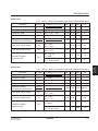
FUNCTIONAL DESCRIPTION
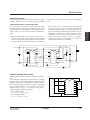
Oscillator
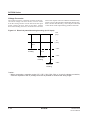
Voltage Multiplier
The voltage multiplier uses the clock signal from the
oscillator to double or triple the input voltage. This requires three external capacitors–two charge-pump capacitors between CAP1+ and CAP1– and CAP2+ and
CAP2–, respectively, and a smoothing capacitor between VI and VO.
External clock
VDD = 0 V
OSC1
OSC1
C1
10 µF
External clock
signal
ROSC
5V
OSC2
OSC2
Reference Volatge Generator and Voltage
Regulator
The reference voltage generator supplies a reference
voltage to the voltage regulator to control the output.
This voltage can be switched ON and OFF.
C2
10 µF
+
+
VI = –5 V
1
14
2
13
3
12
4
11
5
10
6
9
7
8
+
ROSC
1 MΩ
R1
R2
RRV
100 kΩ
to
1 MΩ
+ C4
10 µF
VREG = –8 V
VO = –15 V
C3
10 µF
Double voltage potential levels
VDD
POFF
RV
VCC
(+5V)
Control signal
RRV = 100 kΩ to 1 MΩ
GND
VREG
(–5V)
VDD = 0 V
VI = –5 V
VCAP2 – = 2VI = –10 V
Tripled voltage potential levels
VDD = 0 V
VI = –5 V
VO = 3VI = –15 V
SCI7000 Series
Technical Manual
EPSON
2–11
DC/DC Converter
& Voltage Regulator
Oscillator
The on-chip RC oscillator network frequency is determined by the external resistor, ROSC, connected between OSC1 and OSC2. This oscillator can be disabled
in favor of an external clock by leaving OSC2 open and
applying an external clock signal to OSC1.
SCI7661 Series
TYPICAL APPLICATIONS
Voltage Tripler with Regulator
The following figure shows the circuit required to triple
the input voltage, regulate the result and add a temperature gradient of –0.4%/°C. Note that the high input impedance of RV requires appropriate noise countermeasures.
Converting a Voltage Tripler to a Voltage
Doubler
To convert this curcuit to a voltage doubler, remove capacitor C2 and short circuit CAP2– to VO.
VDD = 0 V
VDD = 0 V
5V
C1
10 µF
+
C2
10 µF
+
1
+
C2
10µF
+
1
14
2
13
3
12
4
11
5
10
6
9
14
2
13
3
12
4
11
5
10
6
9
7
VI = –5 V
C1
10µF
8
+
ROSC
1 MΩ
R1
R2
5V
RRV
100 kΩ
to
1 MΩ
+ C4
10 µF
VI = –5 V
VREG = –8 V
VO = –15 V
=
7
VO = –15 V
8
+
RRV
VRV
R1
ROSC
1 MΩ
C3
10 µF
C3
10 µF
Parallel Connection
Connecting two or more chips in parallel reduces the
output impedance by 1/n, where n is the number of devices used.
Only the single output smoothing capacitor, C3, is re-
quired when any number of devices are connected in
parallel. Also, the voltage regulator in one chip is sufficient to regulate the combined output.
VDD = 0 V
5V
VI = –5 V
C1 +
10 µF
1
14
2
13
C2 +
10 µF
3
12
4
11
5
10
9
6
9
8
7
8
C1 +
10 µF
1
14
2
13
C2 +
10 µF
3
12
4
11
5
10
6
7
ROSC
1 MΩ
ROSC
1 MΩ
RRV
100 kΩ
to
1 MΩ
+
C4
10 µF
VREG = –10 V
VO = –15 V
+C3
10 µF
2–12
EPSON
SCI7000 Series
Technical Manual
SCI7661 Series
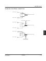
Serial Connection
connection, however, this also raises the output impedance.
<Precautions when connecting loads>
In case of series connections, when connecting loads
between the first stage VDD (or other potential of the
second stage VDD or up) and the second stage VREG as
shown in Fig. 2-13, be cautions about the following
point.
the first stage VDD (or other potential of the second
stage VDD or up) to cause a voltage exceeding the
absolute maximum rating for the second stage VDD at
the VREG terminal, normal operation of the IC may be
hampered. Consequently, When making a series
connection, insert a diode D1 between the second
stage VI and VREG as shown in Fig. 2-13 so that a
voltage exceeding the second stage VDD or up may
not be applied to the VREG terminal.
* When normal output is not occurring at the VREG terminal such as at times of starting up or when turning
the VREG off by Poff signals, if current flows into the
second stage VREG terminal through the load from
V'DD = VI = –5V
VDD = 0V
10µF
5V
1
10µF
2
13
3
12
4
11
5
10
6
10µF
+
7
+
1
14
–
2
13
+
3
12
–
4
11
5
10
6
9
7
8
1MΩ
10µF
9 VO = –10V= VI
8
+
VI = –5V
14
–
100kΩ
to
1MΩ
Load
+
+
–
–
10µF
V'REG = –15V
VO = –20V
–
10µF
D1
Positive Voltage Conversion
Adding diodes converts a negative voltage to a positive
one.
To convert the voltage tripler shown earlier to a voltage
doubler, remove C2 and D2, and short circuit D3. Small
Schottky diodes are recommended for all three diodes.
The resulting voltage is lowered by VF, the voltage drop
in the forward direction for each diode used. For example, if VDD = 0V, VI = –5V, and VF = 0.6V, the resulting voltages would be as follows.
• For a voltage tripler,
VO = 10 – (3 × 0.6) = 8.2V
• For a voltage doubler,
VO = 5 – (2 × 0.6) = 3.8V
SCI7000 Series
Technical Manual
VDD = 0 V
C1
10 µF
D1
+
D2
C2
10 µF
5V
+
D3
+
VO = 8.2 V
1
14
2
13
3
12
4
11
5
10
6
9
7
8
ROSC
1 MΩ
C3
10 µF
VI = –5 V
EPSON
2–13
DC/DC Converter
& Voltage Regulator
Connecting two or more chips in series obtains a higher
output voltage than can be obtained using a parallel
SCI7661 Series
Simultaneous Voltage Conversion
Using an External Gradient
Combining a standard voltage tripler circuit with one
for positive voltage conversion generates both –15 and
8.2V outputs from a single input, however, it also raises
the output impedance.
A voltage doubler generates –10 and 3.8V outputs.
The SCI7661C0B/M0B offers three built-in temperature
gradients— –0.1, –0.4 and –0.6%/°C.
To set the gradient externally, place a thermistor, RT, in
series with the variable resistor, RRV, used to adjust the
output voltage.
VDD = 0 V
10 µF
+
D2
10 µF
10 µF
+
D3
+ 10 µF
+
10 µF
5V
+
D1
1
14
2
13
3
12
4
11
5
10
6
9
7
8
ROSC
1 MΩ
VO1 = –15 V
1
14
2
13
3
12
4
11
5
10
6
9
7
8
VDD
R1
+
10 µF
RRV
RT
RP
VREG
VO2 = 8.2 V
+ 10 µF
VI = –5 V
Potential levels
VO2 = 8.2V
VDD = 0 V
VI = –5 V
VO1 = –15 V
2–14
EPSON
SCI7000 Series
Technical Manual
SCI7654 Series
• Input voltages
The SCI7654 C0A/M0A is a CMOS process, chargepumping DC/DC converter and voltage regulator featuring the very high efficiency but low power consumption. An addition of four, three, or two external capacitors can generate four-, three- or two-time output voltage in negative direction than the input voltage. Also,
the built-in voltage regulator can set any output voltage
of DC/DC converter and can output the regulated voltage using two external resistances. As the regulator
output can have a negative temperature gradient that is
required for LCD panels, it is optimum for the LCD
panel power supply.
FEATURES
SCI7000 Series
Technical Manual
• DC/DC converter output
voltage
•
•
•
• Charge-pumping, DC-to-DC converter (four-, threeor two-time negative boosting)
• Built-in voltage regulator (regulated voltage output
circuit)
• High power conversion
efficiency
: 95%
• Low current consumption : 130 µA (VI = –5.0 V
during four-time
boosting, Typ.)
• High output capacity
: 20 mA (Max.)
: –2.4 to –5.5 V (during
four-time boosting)
: 2.4 to –7.3 V (during
three-time boosting)
: 2.4 to –11 V (during
two-time boosting)
•
•
•
: |Input voltage| × 4
(Max.)
Built-in reference voltage for
high-precision regulator : 1.5 + –0.05 V (at CT0)
Temperature gradient
function of regulator
output voltages
: –0.04, –0.15, –0.35,
–0.55 (%/°C)
Low standby current
(during power-off)
: 5.0 µA
Power-off by the external signal
Full built-in oscillator circuit
Lineup
: SCI7654M 0A , 16-pin
SSOP
: SCI7654C 0A , 16-pin
DIP
APPLICATIONS
• Power supply of medium- and small-capacity LCD
panels
• Regulated power supply of battery driven devices
EPSON
2–15
DC/DC Converter
& Voltage Regulator
DESCRIPTION
SCI7654 Series
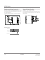
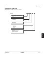
BLOCK DIAGRAM
Figure 2.1 Block diagram
VDD
POFF1
POFF2
FC
Reference
voltage
circuit
Power-off
control circuit
Clock
generator
circuit
TC1
TC2
RV
Booster control
circuit
Voltage
regulation
circuit
VREG
VRI
Voltage converter
circuit
VI
C1P
C1N
C3N
VO
C2P
C2N
PIN DESCRIPTION
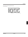
Figure 2.2 SCI7654M0A/C0A pin assignment
2–16
VO
1
16
C2P
VRI
2
15
C2N
VREG
3
14
C3N
RV
4
13
C1N
VDD
5
12
C1P
FC
6
11
VI
TC1
7
10
POFF1
TC2
8
9
POFF2
EPSON
SCI7000 Series
Technical Manual
SCI7654 Series
Table 2.1 Functions of the terminal
Function
VO
1
18
Four-time booster output
VRI
2
19
Regulator input
VREG
3
20
Regulator output
RV
4
21
Regulator output voltage adjustment input
VDD
5
22, 23
FC
6
24
Internal clock frequency input, and clock input in serial/parallel
connection
TC1
7
3
Regulator output temperature gradient setup input (1)
TC2
8
4
Regulator output temperature gradient setup input (2)
POFF2
9
5
Power-off control input (2)
POFF1
10
6
Power-off control input (1)
VI
11
11, 12
Power voltage (negative)
C1P
12
13
Two- or four-time booster capacitor positive pin
C1N
13
14
Two-time booster capacitor negative pin
C3N
14
15
Four-time booster capacitor negative pin
C2N
15
16
Three-time booster capacitor negative pin
C2P
16
17
Three-time booster capacitor positive pin
SCI7000 Series
Technical Manual
DC/DC Converter
& Voltage Regulator
Pin name Pin No. PAD No.
Power pin (positive)
EPSON
2–17
SCI7654 Series
Table 2.2 Absolute maximum ratings
VDD reference
Parameter
Symbol
Rating
Min.
Max.
Unit
Remarks
Input power voltage
VI
–26.0/N
VDD + 0.3
V
N = Boost time
VI pin
Input pin voltage
V1
VI – 0.3
VDD + 0.3
V
POFF1, POFF2, TC1,
TC2 and FC pins
Output pin voltage 1
VOC1
VI – 0.3
VDD + 0.3
V
C1P and C2P pins
Output pin voltage 2
VOC2
2 × VI – 0.3
VI + 0.3
V
C1N pin
Output pin voltage 3
VOC3
3 × VI – 0.3
2 × VI + 0.3
V
C2N pin
Output pin voltage 4
VOC4
4 × VI – 0.3
3 × VI + 0.3
V
C3N pin
Regulator input power
voltage
VRI
N × VI – 0.3
VDD + 0.3
V
N = Boost time, VRI pin
Regulator input pin voltage
VRV
N × VI – 0.3
VDD + 0.3
V
N = Boost time, RV pin
Output voltage
VO
N × VI – 0.3
VDD + 0.3
V
N = Boost time
VO and VREG pins
Input current
II
80
mA
VI pin
Output current
IO
N ≤ 4: 20
N > 4: 80/N
mA
N = Boost time
VO and VREG pins
Allowable loss
Pd
210
mW
Ta ≤ 25°C
Operating temperature
Topr
–30
85
°C
Storage temperature
Tstg
–55
150
°C
Soldering temperature
and time
Tsol
260 • 10
°C • S
At leads
Notes: 1. An operation exceeding the above absolute maximum ratings may cause a malfunction or
permanent damage of devices. The device reliability may drop excessively even if the devices
temporarily operate normally.
2. Electrical potential to peripheral systems:
The SCI7654 common power supply has the highest potential (VDD). The electrical potential
given by this specification is based on VDD = 0 V. Take care to avoid a potential problem
during connection to a peripheral system.
2–18
EPSON
SCI7000 Series
Technical Manual
SCI7654 Series
Figure 2.3 Potential relationship
VCC
System
SCI7654
VDD
(0 V)
(+5 V)
5V
VI
(–5 V)
DC/DC Converter
& Voltage Regulator
GND
(0 V)
10 V
–10 V
Two-time
boosting
15 V
–15 V
Three-time
boosting
20 V
Four-time
boosting
ELECTRICAL CHARACTERISTICS
Table 2.3 DC characteristics (1)
Parameter
Input power voltage
Boost start input power
voltage
Symbol
VI
VSTA
Ta = –30°C to +85°C, VDD = 0 V, VI = –5.0 V
unless otherwise noted
Characteristics
Min.
–22/N
–2.4
V
N = Boost time if CT1 is selected
–22/N
–2.4
V
N = Boost time if CT2 is selected
–22/N
–2.4
V
N = Boost time if CT3 is selected
–22/N
–2.4
V
N = Boost time, FC = VDD during
no loading
–22/N
–2.4
V
VO
–22
Regulator input voltage
VRI
–22
SCI7000 Series
Technical Manual
VREG
Max. Unit
N = Boost time if CT0 is selected
Boost output voltage
Regulator output voltage
Typ.
IREG = 0, VRI = –22 V
RRV = 1MΩ
EPSON
V
–2.4
V
–2.4
V
2–19
SCI7654 Series
Table 2.3 DC characteristics (2)
Ta = –30°C to +85°C, VDD = 0 V, VI = –5.0 V
unless otherwise noted
Parameter
Boost output impedance
Boost power conversion
efficiency
Booster operation current
consumption 1
Booster operation current
consumption 2
Regulator operation
current consumption
Symbol
RO
Peff
Iopr1
Iopr2
IOPVR
Characteristics
Min.
Typ.
Max. Unit
IO = 10 mA, VI = –5.0 V during
4-time boosting
C1, C2, C3, CO = 10 µF (tantalum)
200
300
Ω
IO = 10 mA, VI = –3.0 V,
Ta = 25°C during 4-time boosting
C1, C2, C3, CO = 10 µF (tantalum)
250
300
Ω
IO = 2 mA, VI = –5.0 V during
4-time boosting
C1, C2, C3, CO = 10 µF (tantalum)
95
%
IO = 2 mA, VI = –3.0 V, Ta = 25°C
during 4-time boosting
C1, C2, C3, CO = 10 µF (tantalum)
94
%
FC = VDD, POFF1 = VI, POFF2 = VDD,
VI = –5.0 V during no loading
C1, C2, C3, CO = 10 µF (tantalum)
130
220
µA
FC = VDD, POFF1 = VI, POFF2 = VDD,
VI = –3.0 V, Ta = 25°C during no loading
C1, C2, C3, CO = 10 µF (tantalum)
90
150
µA
FC = VI, POFF1 = VI, POFF2 = VDD,
VI = –5.0 V during no loading
C1, C2, C3, CO = 10 µF (tantalum)
520
880
µA
FC = VI, POFF1 = VI, POFF2 = VDD,
VI = –3.0 V, Ta = 25°C during no loading
C1, C2, C3, CO = 10 µF (tantalum)
360
600
µA
VRI = –20 V, RRV = 1 MΩ during
no loading
10
15
µA
Static current
IQ
POFF1 = VI, POFF2 = VI
FC = VDD
5.0
µA
Input leakage current
ILI
Pins used: POFF1, POFF2, FC,
TC1, TC2
0.5
µA
20
Ω
0.2
%/V
Regulated output
saturation resistance
0 < IREG < 20 mA
RSAT (*1) RV = VDD
Ta = 25°C
Regulated output
voltage stability
–20 V < VRI < –10 V, IREG = 1 mA
∆VR (*2) VREG = –9 V
Ta = 25°C
2–20
EPSON
10
SCI7000 Series
Technical Manual
SCI7654 Series
Table 2.3 DC characteristics (3)
Ta = –30°C to +85°C, VDD = 0 V, VI = –5.0 V
unless otherwise noted
Regulated output load
variation
Symbol
Characteristics
Min.
VRI = –20 V, VREG = –15 V,
∆VO (*3) Ta = 25°C setup
0 < IREG < 20 mA
Reference voltage
(Ta = 25°C)
Reference voltage
temperature coefficient
(*4, *5)
30
Max. Unit
50
mV
VREF0
TC1 = VDD, TC2 = VDD
–1.55 –1.50 –1.45
V
VREF1
TC1 = VDD, TC2 = VI
–1.70 –1.50 –1.30
V
VREF2
TC1 = VI, TC2 = VDD
–1.90 –1.50 –1.10
V
VREF3
TC1 = VI, TC2 = VI
–2.15 –1.50 –0.85
V
CT0
TC1 = VDD, TC2 = VDD, SSOP product
–0.07 –0.04
CT1
TC1 = VDD, TC2 = VI, SSOP product
–0.25 –0.15 –0.07 %/°C
CT2
TC1 = VI, TC2 = VDD, SSOP product
–0.45 –0.35 –0.20 %/°C
CT3
TC1 = VI, TC2 = VI, SSOP product
–0.75 –0.55 –0.30 %/°C
VI
VI = –2.4 to –5.5 V
Pins used: POFF1, POFF2, FC,
TC1, TC2
0.2 VI
VIL
VI = –2.4 to –5.5 V
Pins used: POFF1, POFF2, FC,
TC1, TC2
0.8 VI
V
CMAX
Capacitors used: C1, C2 and C3
47
µF
Input voltage level
Booster capacitance
Typ.
0
%/°C
V
∆ (VREG – VRI)
∆IREG
*1
RSAT =
*2
∆VR =
VREG (VRI = –20 V) – VREG (VRI = –10 V)
∆VRI • VREG (VRI = –10 V)
*3
∆VO =
VREG (IREG = 20 mA) – VREG (IREG = 0 mA)
∆IREG
*4
CT =
*5
The reference voltage and temperature coefficient of the chip products may vary depending on the moldings used on each chip. Use these chips only after the temperature test.
SCI7000 Series
Technical Manual
| VREF (50°C) | – | VREF (0°C) |
50°C – 0°C
×
100
| VREF (25°C) |
EPSON
2–21
DC/DC Converter
& Voltage Regulator
Parameter
SCI7654 Series
Table 2.4 AC characteristics
VDD = 0 V and VI = –5.0 V
unless otherwise noted
Parameter
Internal clock frequency 1
Symbol
fCL1
Characteristics
FC = VDD,
POFF1 = VI
POFF2 = VDD
Pin used: C1P
Internal clock frequency 2
fCL2
FC = VI,
POFF1 = VI
POFF2 = VDD
Pin used: C1P
Min.
Typ.
Max. Unit
Ta = 25°C
3.0
4.0
6.0
kHz
Ta = –30°C
to +85°C
2.0
4.0
7.0
kHz
Ta = 25°C
12.0
16.0
24.0
kHz
Ta = –30°C
to +85°C
8.0
16.0
28.0
kHz
EXPLANATION OF FUNCTIONS
Clock Generator Circuit
As the SCI7654 has a built-in clock generator circuit, no
more parts are required for voltage boost control. The
clock frequency changes according to the FC pin voltage level as defined on Table 2.5. Low Output mode or
High Output mode is selectable. This allows frequency
selection according to the used capacitance and load
current as the boost output impedance changes depending on the clock frequency and external booster capacitance. However, the High Output mode has the current
consumption approximately four times larger than the
Low Output mode.
Table 2.5 FC pin setup
Characteristics
FC pin
Mode
Clock frequency
H (VDD)
Low Output
4.0 kHz (Typ.)
L (VI)
High Output
16.0 kHz (Typ.) IOP × Approx. 4 VRI × Approx. 1/4 See Figure A1. See Figure A1.
Current
Output
Output ripple
Capacitance
consumption
impedance
IOP (*1)
VRR (*2)
See Figure A1. See Figure A1.
*1 See the DC characteristics table for current consumption.
*2 See Section Page 2-32 for the output ripple definition and calculation.
2–22
EPSON
SCI7000 Series
Technical Manual
SCI7654 Series
Figure A1 Characteristic chart: Capacitance vs. output impedance when 4X pressure is applied
NOTE:
This characteristic chart simply indicates an approximate trend in the characteristics, which
may vary depending on evaluation environment, parts used, and other factors.
Capacitance vs. output impedance characteristic when 4X pressure is applied
Load current = 10 mA, Ta = 25°C, C1 = C2 = C0
Capacitor used: Tantalum electrolytic capacitor
DC/DC Converter
& Voltage Regulator
550
500
Output impedance [Ω]
450
400
350
300
250
200
150
1
10
100
C [µF]
SCI7000 Series
Technical Manual
VI = –3.0V FC = "H"
VI = –3.0V FC = "L"
VI = –5.0V FC = "H"
VI = –5.0V FC = "L"
EPSON
2–23
SCI7654 Series
Voltage Converter
The voltage converter, consisting of a boost control circuit and a voltage converter circuit, receives clocks
from the clock generator circuit and boosts the input
power voltage (VI) four, three or two times. During
four-time boosting, however, the three-time and two-
time boost outputs cannot be obtained simultaneously.
Figure 2.4 gives the potential relationship during four-,
three- and two-time boosting. The C2P pin is also used
as the master clock output during parallel connection.
Figure 2.4 Electrical potentials during boosting (at -5V input)
VDD
(0 V)
VI
(–5 V)
10 V
–10 V
Two-time
boosting
15 V
–15 V
Three-time
boosting
20 V
–20 V
Four-time
boosting
Caution:
• When connecting a capacitor to the C1P, C2P, C1N, C2N, C3N, or VO pin for voltage conversion,
close the capacitor to the IC package as much as possible to minimize the wiring length.
2–24
EPSON
SCI7000 Series
Technical Manual
SCI7654 Series
Reference Voltage Circuit
The SCI7654 has a built-in reference voltage circuit for
voltage regulation. The regulated voltage (explained in
the next “voltage regulator circuit” section) is set depending on the division ratio between this reference
voltage and the external resistance. The reference voltage can be used to change the temperature coefficient at
pins TC1 and TC2. One of four states can be selected as
listed on Table 2.6.
Reference voltage,
VREF (V)
Temperature coefficient,
CT (%/°C)
TC1
(H = VDD)
(L = VI)
TC2
(H = VDD)
(L = VI)
Min.
Typ.
Max.
Min.
Typ.
Max.
CT0
H
H
–1.55
–1.5
–1.45
–0.07
–0.04
0
CT1
H
L
–1.70
–1.5
–1.30
–0.25
–0.15
–0.07
CT2
L
H
–1.90
–1.5
–1.10
–0.45
–0.35
–0.20
CT3
L
L
–2.15
–1.5
–0.85
–0.75
–0.55
–0.30
Mode
Notes: 1. The reference voltage is given at Ta = 25°C.
2. The reference voltage and temperature coefficient of the chip products may vary depending
on the moldings used on each chip. Use these chips only after the temperature test.
The temperature coefficient (CT) is defined by the following equation. The negative sign of the temperature coefficient (CT) means that the |VREF| value decreases when the temperature rises.
CT =
| VREF (50°C) | – | VREF (0°C) |
50°C – 0°C
×
100
| VREF (25°C) |
Notes on TC1 and TC2 pin replacement:
• When replacing the TC1 and TC2 pins after power-on, always select the power-off mode (POFF1 = POFF2 =
VI) and replace them by each other.
Voltage Regulator Circuit
The voltage regulator circuit regulates a voltage entered
in the VRI pin and can output any voltage. It uses the
series voltage regulation. As shown in Figure 2.5, the
VRI and VO pins must be short-circuited by a jumper as
short as possible except for larger time boosting by using external diodes.
As shown by equation (1), any output voltage can be set
by the ratio of external division resistors R1 and R2.
The sum of division resistance is recommended to be
SCI7000 Series
Technical Manual
small as possible to avoid an external noise interference. As the current consumed by division resistors
(equation (2)) flows, the 100 ohms to 1M ohms are recommended to use.
The temperature coefficient of the regulated voltage is
equal to the temperature coefficient of the reference
voltage that is explained in the “reference voltage circuit” section.
EPSON
2–25
DC/DC Converter
& Voltage Regulator
Table 2.6 Setup of reference voltage and temperature coefficient
SCI7654 Series
Figure 2.5 VREG setup and mounting notes
R1
R2
1 VO
C2P 16
2 VRI
C2N 15
3 VREG
C3N 14
4 RV
C1N 13
5 VDD
C1P 12
6 FC
VI 11
7 TC1
POFF1 10
8 TC2
POFF2 9
Setup:
• Relationship between VREG and reference voltage
R1 + R2
VREG =
× (Reference voltage)
R1
• Current consumption of division resistors
| VREG |
IREG =
R1 + R2
• • • • Equation (1)
• • • • Equation (2)
Setup example:
• To output VREG = –18 V by four-time boosting if VI = –5 V and VO = –20 V
First, determine the total resistance of division resistors R1 and R2. If the current consumption is assumed to be 20
µA, the total resistance can be obtained from equation (2) as follows:
R1 + R2 = 12V ÷ 20 µA = 900 kΩ
If the reference voltage is -1.5 V, the division resistance ratio can be obtained from equation (1) as follows:
(R1 + R2) / R2 = (–18 V) ÷ (–1.5 V) = 12
Therefore, R1 and R2 are:
R1 = 75 kΩ
R2 = 825 kΩ
2–26
EPSON
SCI7000 Series
Technical Manual
SCI7654 Series
Changing the temperature coefficient:
• The temperature coefficient of the regulated voltage depends on the temperature coefficient of the reference
voltage (if the division ratio of setup resistors does not depend on the temperature). It is necessary to change the
temperature coefficient using thermistors, resistors or others to set any other temperature coefficient of the
regulated voltage. The following explains how to calculate the VREG voltage in temperature T.
T0
CTR1
CTR2
CTREF
R1 (T0)
R2 (T0)
VREF (T0)
{ 1 + CC
TR2
TR1
:
:
:
:
:
:
:
× R2 (T0)
× CTREF × (T – T0) × VREF (T0)
× R1 (T0)
}
• • • • Equation (3)
DC/DC Converter
& Voltage Regulator
VREG (T) =
25°C
Temperature coefficient of resistor R1 (Ratio to the value at 25°C)
Temperature coefficient of resistor R2 (Ratio to the value at 25°C)
Temperature coefficient of internal reference voltage (%/°C)
R1 value (Ω) at 25°C
R2 value (Ω) at 25°C
Internal reference voltage (V) at 25°C
If the temperature coefficient of R1 and R2 is identical in equation (3), the VREG voltage depends on the temperature coefficient of internal reference voltage only.
Application notes on voltage regulator circuit:
• To satisfy the absolute maximum ratings of the SCI7654, the setup resistor(s) must be inserted between VDD
and VREG pins of the SCI7654 that uses the voltage regulator. The SCI7654 IC itself may be degraded or
destroyed if the R1 resistor is connected to pin VDD of SCI7654 that does not use the regulator during serial
connection.
• The regulation voltage adjustment input (pin RV) has the very high input impedance, and its noise insertion can
drop the regulator stability. As shown in Figure 2.5, shield the cable between the division resistor and RV pin or
use a cable as short as possible between them.
SCI7000 Series
Technical Manual
EPSON
2–27
SCI7654 Series
Power-off Control Function
The SCI7654 has the power-off function and turns on or
off each circuit function when control signals are entered in the POFF1 and POFF2 pins from an external
system (such as microprocessor) as defined on Table
2.7. This power-off function can also cut the reactive
current in parallel connection and other application circuits.
To use the dual-state, power-off control (all ON and all
OFF states) only, connect pin POFF2 to pin VI and use
only pin POFF1 for power-off control.
Table 2.7 Available combination of power-off control
Mode
Functions
POFF1
POFF2
(H = VDD) (H = VDD)
Booster Regulator
(L = VI) (L = VI) Oscillator circuit
circuit
Applications
PS1
H
L
On
On
On
All circuits are turned on.
PS2
L
L
Off
Off (*1)
Off (*2)
All circuits are turned off.
PS3
H
H
Off
On
On
Slave unit side of parallel connection
(Booster and regulator)
PS4
L
H
On
On
Off
Master unit side of parallel
connection (Booster only)
*1 When the booster circuit is off, approximately VI + 0.6 V voltage appears at VO pin.
*2 When the regulator is off, the VREG pin becomes high-impedance state.
Application notes on power-off function:
• When using external system signals for power-on control, start to control the power only when VI voltage
becomes stable after power-on. Unstable VI voltage may destroy the IC permanently during on/off control.
Figure 2.6 Start timing of power-off control
2–28
VI
VI
POFF1
POFF1
POFF2
POFF2
EPSON
SCI7000 Series
Technical Manual
SCI7654 Series
CHARACTERISTICS GRAPHICS
Figure 2.7 Characteristics graphics
200
300
DC/DC Converter
& Voltage Regulator
280
180
Booster output impedance [Ω]
Booster current consumption [µA]
260
160
140
120
100
240
220
200
180
160
80
140
60
40
120
100
0
1
2
3
4
5
7
6
1
Input voltage [V]
2
3
4
5
6
7
Input voltage [V]
Input voltage (VI) -Booster circuit current consumption (Iopr) Input voltage (VI) - Booster output impedance (ROUT)
Peff
(%)
VO
(V)
VO
(V)
VI = –3 V, Four-times Booster
–12.00
Peff
(%)
VI = –5 V, Four-times Booster
100.0
–20.00
100.0
VO
VO
Peff
Peff
50.00
20.00
0
0
0
0
IO (mA)
Power conversion
efficiency (Peff)
Output voltage (VO)
Input current (IO)
IO (mA)
Power conversion
efficiency (Peff)
Output voltage (VO)
Input current (IO)
SCI7000 Series
Technical Manual
50.00
20.00
EPSON
2–29
SCI7654 Series
APPLICATION CIRCUIT EXAMPLES
Four-time Booster and Regulator
Figure 2.8 gives a wiring example of four-time booster
and regulator that is the typical SCI7654 application.
This example boosts the input voltage (VI) four times in
negative direction, and outputs the regulated voltage at
VREG pin.
Figure 2.8 Wiring example of 4-time booster and regulator
CO
+
VREG
CREG
+
R1
R2
VDD
1 VO
C2P 16
2 VRI
C2N 15
3 VREG
C3N 14
4 RV
C1N 13
5 VDD
C1P 12
6 FC
+
CI
+
C2
C3
C1
+
+
VI 11
7 TC1
POFF1 10
8 TC2
POFF2 9
VI
◊ Setup conditions of Figure 2.8
• Internal clock : On (Low Output mode)
• Booster circuit : On
• Regulator
: On (if CT = –0.04%/°C)
◊ Power-off procedure
• Set the POFF1 pin to logical low (VI) to turn off all circuits.
◊ Regulator
• For the regulator setup and notes, see the “voltage regulator circuit” section.
◊ Application in other setup conditions
1 When used in the High Output mode
• Connect the FC pin to the VI pin.
2 When changing the temperature coefficient (CT)
• Change the TC1 and TC2 pin setup by following the definition of Table 2.7.
2–30
EPSON
SCI7000 Series
Technical Manual
SCI7654 Series
4-time Booster
Only the booster circuit operates, and it boosts the input
voltage (VI) four times in negative direction and outputs
it at the VO pin. As the regulator is not used, the voltage
appearing at the VO pin may contain ripple components.
Figure 2.9 gives a wiring example.
Figure 2.9 Wiring example of 4-time booster
CO
VO
VDD
1 VO
C2P 16
2 VRI
C2N 15
3 VREG
C3N 14
4 RV
C1N 13
5 VDD
C1P 12
6 FC
+
CI
DC/DC Converter
& Voltage Regulator
+
+
C2
C3
C1
+
+
VI 11
7 TC1
POFF1 10
8 TC2
POFF2 9
VI
◊ Setup conditions of Figure 2.9
• Internal clock : On (Low Output mode)
• Booster circuit : On
• Regulator
: Off
◊ Power-off procedure
• Set the POFF2 pin to low (VI) to turn off all circuits.
◊ Ripple voltage
• As the output at VO pin is unstable, it can contain ripple components as shown in Figure 2.10. The ripple voltage
(VRP) increases according to the load current, and it can roughly be calculated by equation (4).
SCI7000 Series
Technical Manual
EPSON
2–31
SCI7654 Series
Figure 2.10 Ripple waveforms
VRP
VRP =
IO
2 • fCL • CO
+ IO • RCOUT
• • • • Equation (4)
where,
: Load current (A)
IO
fCL
: Clock frequency (Hz)
RCOUT : Serial equivalent resistance (Ω) of output capacitor CO
◊ Application in other setup conditions
1 When used in the High Output mode
• Connect the FC pin to the VI pin.
Parallel Connection (for Increased Boosting)
The parallel connection is useful for reduction of
booster output impedance or reduction of ripple voltage. In the parallel connection of “n” lines, the booster
output impedance can be reduced to approximately “1/
n". Only the smoothing capacitor (CO) for booster output can be used commonly in the parallel connection.
When using the regulator, use only one of “n” SCI7654
chips which are in parallel connection. (If multiple
regulators are operated in parallel mode, the reactive
current consumption occurs.) Figure 2.11 gives a wiring example of 4-time booster and regulator where two
SCI7654's are parallelly connected.
Figure 2.11 Parallel connection example
VREG
+
CO
VDD
1 VO
C2P 16
+
2 VRI
C2N 15
C2
3 VREG
C3N 14
4 RV
C1N 13
5 VDD
C1P 12
6 FC
+
CI
CREG
+
R1
C3
+
C1
+
VI 11
R2
1 VO
C2P 16
+
2 VRI
C2N 15
C2
3 VREG
C3N 14
4 RV
C1N 13
5 VDD
C1P 12
6 FC
C3
+
C1
+
VI 11
7 TC1
POFF1 10
7 TC1
POFF1 10
8 TC2
POFF2 9
8 TC2
POFF2 9
VI
2–32
EPSON
SCI7000 Series
Technical Manual
SCI7654 Series
◊ Setup conditions of Figure 2.11
First stage
• Internal clock : On (Low Output mode)
• Booster circuit : On
• Regulator
: Off
Second stage
• Internal clock : Off
• Booster circuit : On
• Regulator
: On (if CT = –0.04%/°C)
• In Figure 2.11, when the POFF2 pin of the first-stage SCI7654 is set to low (VI), voltage boosting is stopped at
the first and second stages. However, the regulator at the second stage does not stop. Therefore, the voltage that
is approximately VI appears at VREG pin during |VREG| > |VI| setup.
• To set the VREG pin to high-impedance state, set both POFF1 and POFF2 pins to low at the first and second
stages.
◊ Application in other setup conditions
1 When used in the High Output mode
• Connect the FC pin of the first-stage SCI7654 to the VI pin.
2 When changing the temperature coefficient (CT)
• Change the TC1 and TC2 pin setup by following the definition of Table 2.7.
Larger Time Boosting Using Diodes
The SCI7654 can be configured to have the five-time or
larger voltage boosting and regulation by adding external diodes. As the booster output impedance increases
due to the diode forward voltage drop (VF), the diodes
having a smaller VF are recommended to use.
Figure 2.12 gives a wiring example of 6-time booster
and regulator that use two diodes. The wiring between
VO and VRI must be minimal. Figure 2.13 provides the
potential relationship.
Figure 2.12 Wiring example for 6-time boosting using diodes
VO'
VREG
CREG
+
R1
1 VO
C2P 16
2 VRI
C2N 15
3 VREG
C3N 14
4 RV
C1N 13
5 VDD
C1P 12
R2
VDD
6 FC
+
CI
C4
+
D1
D2
+
C2
C1
C3
C5
CO
+
+
+
+
VI 11
7 TC1
POFF1 10
8 TC2
POFF2 9
VI
SCI7000 Series
Technical Manual
EPSON
2–33
DC/DC Converter
& Voltage Regulator
◊ Power-off procedure
SCI7654 Series
◊ Setup conditions of Figure 2.12
• Internal clock : On (Low Output mode)
• Booster circuit : On
• Regulator
: On (if CT = –0.04%/°C)
Figure 2.13 Potential relationship during 6-time boosting using diodes
VDD
VI
VI
4VI
6VI – (2∗VF)
VO
6VI
VO'
2∗VF
◊ Power-off procedure
• Set the POFF1 pin to low (VI) to turn off all circuits.
◊ Output voltages
• When diodes are used for voltage boosting, the characteristics of diodes directly affect on the voltage boosting
characteristics. The forward voltage drop (VF) of diodes can reduce the booster output voltage. As the example
of Figure 2.12 uses two diodes, the drop of “VF” voltage multiplied by two occurs as shown in Figure 2.13. The
booster output voltage is expressed by equation (5).
To increase the |VO'| value, use the diodes having a smaller VF.
| VO' | = 6 × | VI | – 2 × VF
• • • • Equation (5)
◊ Notes
1 Input and output current conditions
To satisfy the input and output current ratings, limit the total current does not exceed the rated input current.
The total current means the total boost time multiplied by the output load current. The example of Figure 2.12
has the maximum load current of 13.3 mA ( = 80 mA divided by 6).
2 Input and output voltage conditions
To satisfy the input and output voltage ratings, take care not to violate the electric potential relationship of
higher time boosting using diodes. The example of Figure 2.12 must have the “VI” that can satisfy the input
voltage conditions during 6-time boosting (see Table 2.3).
◊ Application in other setup conditions
1 When used in the High Output mode
Connect the FC pin to the VI pin.
2 When changing the temperature coefficient (CT)
Change the TC1 and TC2 pin setup by following the definition of Table 2.7.
2–34
EPSON
SCI7000 Series
Technical Manual
SCI7654 Series
Positive Voltage Conversion
The SCI7654 can also boost up a voltage to the positive
potential using external diodes. In such case, however,
the regulator function is unavailable. Figure 2.14 gives
a wiring example for three-time positive boosting, and
Figure 2.15 provides its electrical potential relationship.
Figure 2.14 Wiring example of positive voltage conversion (3-time boosting)
D1
D2
D3
C1
VDD
1 VO
C2P 16
2 VRI
C2N 15
3 VREG
C3N 14
4 RV
C1N 13
5 VDD
C1P 12
6 FC
+
CI
DC/DC Converter
& Voltage Regulator
VO'
+
C2
+
+
CO
VI 11
7 TC1
POFF1 10
8 TC2
POFF2 9
VI
◊ Setup conditions of Figure 2.14
• Internal clock : On (Low Output mode)
• Booster circuit : On
• Regulator
: Off
Figure 2.15 Potential relationship during positive voltage conversion (3-time boosting)
3∗VF
3VI
VDD
VO'
3VI – (3∗VF)
VI
VI
◊ Power-off procedure
• Set the POFF2 pin to low (VI) to turn off all circuits.
◊ Two-time boosting
• To boost up a voltage two times, remove capacitor C1 and diode D1 of Figure 2.14, and connect the anode of
diode D2 to the VDD pin.
SCI7000 Series
Technical Manual
EPSON
2–35
SCI7654 Series
◊ Output voltages
• When diodes are used for voltage boosting, the characteristics of diodes directly affect on the voltage boosting
characteristics. The forward voltage drop (VF) of diodes can reduce the booster output voltage. As the example
of Figure 2.14 uses three diodes, the drop of “VF” voltage multiplied by three occurs. The booster output
voltage is expressed by equation (5).
To increase the |VO'| value, use the diodes having a smaller VF.
| VO' | = 3 × | VI | – (3 × VF)
• • • • Equation (6)
◊ Notes
1 Input and output current conditions
To satisfy the input and output current ratings, take care to limit the input current below the ratings.
2 Input and output voltage conditions
During forward voltage conversion, the input voltage ratings are the same as two-time negative voltage boosting (see Table 2.3).
◊ Application in other setup conditions
When used in the High Output mode, connect the FC pin to the VI pin.
Wiring Example When Changing the
Regulator Temperature Coefficient
voltage. To set another temperature coefficient, use a
thermistor resistor or others as shown in Figure 2.16.
The temperature coefficient of the regulator depends on
the temperature coefficient of the internal reference
Figure 2.16 Wiring example when changing the regulator temperature coefficient
CO
+
VREG
CREG
+
R1
RP
R2
RT
VDD
1 VO
C2P 16
+
2 VRI
C2N 15
C2
3 VREG
C3N 14
4 RV
C1N 13
5 VDD
C1P 12
6 FC
+
CI
C3
C1
+
+
VI 11
7 TC1
POFF1 10
8 TC2
POFF2 9
VI
2–36
EPSON
SCI7000 Series
Technical Manual
SCI7654 Series
◊ Setup conditions of Figure 2.16
• Internal clock
• Booster circuit
• Regulator
• Thermistor resistor
:
:
:
:
On (Low Output mode)
On
On
RT
◊ Power-off procedure
◊ Regulator temperature coefficient
• For the regulator setup and notes, see the “voltage regulator circuit” section of the function.
• The thermistor resistor (RT) has the non-linear temperature characteristics. To correct them to the linear characteristics, insert the RP as shown Figure 2.16.
◊ Application in other setup conditions
• When used in the High Output mode, connect the FC pin to the VI pin.
SCI7000 Series
Technical Manual
EPSON
2–37
DC/DC Converter
& Voltage Regulator
• Set the POFF1 pin to low (VI) to turn off all circuits.
r
g
to
a
l
u
ag
e
eR
lt
Vo
3.
SCI7810Y Series
DESCRIPTION
FEATURES
The SCI7810Y series products are the fixed type positive voltage regulators being developed utilizing the
CMOS silicon gate process. It is mainly consisted of
the reference voltage circuit driven with low operating
current, differential amplifier, transistor for output control and voltage setting resistor.
Output voltage is fixed on ICs. A wide variety of standard voltage products are prepared.
The package used is the SOT89-3 pins plastic package.
• A wide variety of lineups: 12 types are offered in the
range of 2V to 6V.
• Low operating current: Typ. 1.5 µA (VDD = 5.0V).
• Smaller difference between the input and output voltage: Typ. 0.02V (IO = 10 mA, VO = 5.0V).
• Built-in, highly stable reference voltage source: Typ.
1.0V.
• Smaller temperature factor on output voltage: Typ. –
100 ppm/°C.
• Wider operating voltage range: Maximum 15V.
VDD
(2pin)
Voltage
Regulator
BLOCK DIAGRAM
VO
(3pin)
+
–
Vref
VSS
(1pin)
SCI7000 Series
Technical Manual
EPSON
3–1
SCI7810Y Series
MODEL CLASSIFICATION
Product name
Output voltage
Min.
Typ.
Max.
SCI7810YAA
5.75
6.00
6.25
SCI7810YBA
4.90
5.00
5.10
SCI7810YMA
4.40
4.50
4.60
SCI7810YPA
3.90
4.00
4.10
SCI7810YKA
3.80
3.90
4.00
SCI7810YNA
3.43
3.50
3.57
SCI7810YTA
3.23
3.30
3.37
SCI7810YCA
3.13
3.20
3.27
SCI7810YDA
2.93
3.00
3.07
SCI7810YRA
2.73
2.80
2.87
SCI7810YLA
2.53
2.60
2.67
SCI7810YFA
2.15
2.20
2.25
SCI7810YGA
1.75
1.80
1.85
SCI7810YHA
1.45
1.50
1.55
PIN DESCRIPTION
Pin Function
Pin No. Pin name
3–2
Pin function
1
VSS
Input voltage pin (negative side)
2
VDD
Input voltage pin (positive side)
3
VO
Output voltage pin
EPSON
SCI7000 Series
Technical Manual
SCI7810Y Series
DESCRIPTION OF FUNCTION
SOT89-3pin
1
2
3
The SCI7810Y series products are the fixed type positive output voltage regulators. They employ the series
regulation approach using CMOS transistors between
the input and output for control of the output.
The voltage divided by the built-in resistors R1 and R2
(VREG ) is fed back to the operational amplifier and
compared against the reference voltage (Vref). This
process enables to control the gate voltage of the output
control transistor so that stable output voltage (VO) independent of input voltage is ensured. Output voltage is
internally fixed and determined by the following formula.
VO =
R1 + R2
• Vref
R1
Voltage
Regulator
Pin Layout
(Output control transistor)
VO
(3pin)
VDD
(2pin)
R2
(VREG)
+
–
(Operational amplifier)
Vref
R1
VSS
(1pin)
SCI7000 Series
Technical Manual
EPSON
3–3
SCI7810Y Series
ABSOLUTE MAXIMUM RATING
Parameter
Symbol
Rating
VDD – VSS
18
Output voltage
VO
VDD + 0.3 to VSS – 0.3
Output current
IO
100
mA
Allowable dissipation
PD
200
mW
Operating temperature
Topr
–30 to +85
°C
Storage temperature
Tstg
–65 to +150
Soldering time
Soldering temperature
Tsol
260°C
10 seconds (at lead)
Input voltage
3–4
EPSON
Unit
V
—
SCI7000 Series
Technical Manual
SCI7810Y Series
ELECTRIC CHARACTERISTICS
SCI7810YAA
(Ta = –30°C to +85°C shall be assumed except where otherwise specified.)
Symbol
VI
Conditions (VSS = 0.0v)
Min.
—
Typ.
—
Max.
15
Unit
V
5.75
6.00
6.25
V
Output voltage
VO
VDD = 8.0V, IO = –10mA
Ta = 25°C
Operating current
IOP
VDD = 6.0V to 15.0V No load
—
1.5
5.0
µA
VO = 6.0V, IO = –10mA
—
0.16
0.32
V
Voltage difference between
input and output
VI – VO
Output voltage temperature
characteristics
∆VO
VO
–300 –100 +100
ppm
/°C
dVO
dVI • VO
Ta = –30°C to +85°C
(At the same temperature level)
VDD = 7.0V to 15.0V
IO = –10mA
—
0.1
—
%/V
Load stability
∆VO
Ta = –30°C to +85°C
(At the same temperature level)
VDD = 8.0V
IO = –1mA to –50mA
—
50
—
mV
Supply voltage regulation
rejection ratio
PSRR
VDD = 8.0V, fin = 50kHz
CL = 10µF, IO = –10mA
—
–40
—
dB
Input voltage stability
SCI7810YBA
(Ta = –30°C to +85°C shall be assumed except where otherwise specified.)
Parameter
Symbol
Conditions (VSS = 0.0v)
Min.
Typ.
Max.
Unit
—
—
15
V
4.90
5.00
5.10
V
VDD = 5.0V to 15.0V No load
—
1.5
5.0
µA
VO = 5.0V, IO = –10mA
—
0.17
0.34
V
Input voltage
VI
Output voltage
VO
VDD = 7.0V, IO = –10mA
Ta = 25°C
Operating current
IOP
Voltage difference between
input and output
VI – VO
Output voltage temperature
characteristics
∆VO
VO
–300 –100 +100
ppm
/°C
dVO
dVI • VO
Ta = –30°C to +85°C
(At the same temperature level)
VDD = 6.0V to 15.0V
IO = –10mA
—
0.1
—
%/V
Load stability
∆VO
Ta = –30°C to +85°C
(At the same temperature level)
VDD = 7.0V
IO = –1mA to –50mA
—
50
—
mV
Supply voltage regulation
rejection ratio
PSRR
VDD = 7.0V, fin = 50kHz
CL = 10µF, IO = –10mA
—
–40
—
dB
Input voltage stability
SCI7000 Series
Technical Manual
EPSON
3–5
Voltage
Regulator
Parameter
Input voltage
SCI7810Y Series
SCI7810YMA
(Ta = –30°C to +85°C shall be assumed except where otherwise specified.)
Parameter
Symbol
Input voltage
Conditions (VSS = 0.0v)
VI
Min.
Typ.
Max.
Unit
—
—
15
V
4.40
4.50
4.60
V
Output voltage
VO
VDD = 6.0V, IO = –10mA
Ta = 25°C
Operating current
IOP
VDD = 4.5V to 15.0V No load
—
1.5
5.0
µA
VO = 4.5V, IO = –10mA
—
0.18
0.36
V
Voltage difference between
input and output
VI – VO
Output voltage temperature
characteristics
∆VO
VO
–300 –100 +100
ppm
/°C
dVO
dVI • VO
Ta = –30°C to +85°C
(At the same temperature level)
VDD = 6.0V to 15.0V
IO = –10mA
—
0.1
—
%/V
Load stability
∆VO
Ta = –30°C to +85°C
(At the same temperature level)
VDD = 6.0V
IO = –1mA to –40mA
—
40
—
mV
Supply voltage regulation
rejection ratio
PSRR
VDD = 6.0V, fin = 50kHz
CL = 10µF, IO = –10mA
—
–40
—
dB
Input voltage stability
SCI7810YPA
(Ta = –30°C to +85°C shall be assumed except where otherwise specified.)
Parameter
Symbol
Conditions (VSS = 0.0v)
Min.
Typ.
Max.
Unit
—
—
15
V
3.90
4.00
4.10
V
VDD = 4.0V to 15.0V No load
—
1.5
5.0
µA
VO = 4.0V, IO = –10mA
—
0.19
0.38
V
Input voltage
VI
Output voltage
VO
VDD = 6.0V, IO = –10mA
Ta = 25°C
Operating current
IOP
Voltage difference between
input and output
VI – VO
Output voltage temperature
characteristics
∆VO
VO
–300 –100 +100
ppm
/°C
dVO
dVI • VO
Ta = –30°C to +85°C
(At the same temperature level)
VDD = 5.0V to 15.0V
IO = –10mA
—
0.1
—
%/V
Load stability
∆VO
Ta = –30°C to +85°C
(At the same temperature level)
VDD = 6.0V
IO = –1mA to –40mA
—
40
—
mV
Supply voltage regulation
rejection ratio
PSRR
VDD = 6.0V, fin = 50kHz
CL = 10µF, IO = –10mA
—
–40
—
dB
Input voltage stability
3–6
EPSON
SCI7000 Series
Technical Manual
SCI7810Y Series
SCI7810YKA
(Ta = –30°C to +85°C shall be assumed except where otherwise specified.)
Symbol
Input voltage
Conditions (VSS = 0.0v)
VI
Min.
Typ.
Max.
Unit
—
—
15
V
3.80
3.90
4.00
V
Output voltage
VO
VDD = 6.0V, IO = –10mA
Ta = 25°C
Operating current
IOP
VDD = 3.9V to 15.0V No load
—
1.5
5.0
µA
VO = 3.9V, IO = –10mA
—
0.19
0.38
V
Voltage difference between
input and output
VI – VO
Output voltage temperature
characteristics
∆VO
VO
–300 –100 +100
ppm
/°C
dVO
dVI • VO
Ta = –30°C to +85°C
(At the same temperature level)
VDD = 5.0V to 15.0V
IO = –10mA
—
0.1
—
%/V
Load stability
∆VO
Ta = –30°C to +85°C
(At the same temperature level)
VDD = 6.0V
IO = –1mA to –40mA
—
40
—
mV
Supply voltage regulation
rejection ratio
PSRR
VDD = 6.0V, fin = 50kHz
CL = 10µF, IO = –10mA
—
–40
—
dB
Input voltage stability
SCI7810YNA
(Ta = –30°C to +85°C shall be assumed except where otherwise specified.)
Parameter
Symbol
Conditions (VSS = 0.0v)
Min.
Typ.
Max.
Unit
—
—
15
V
3.43
3.50
3.57
V
VDD = 3.5V to 15.0V No load
—
1.5
5.0
µA
VO = 3.5V, IO = –10mA
—
0.21
0.42
V
Input voltage
VI
Output voltage
VO
VDD = 5.0V, IO = –10mA
Ta = 25°C
Operating current
IOP
Voltage difference between
input and output
VI – VO
Output voltage temperature
characteristics
∆VO
VO
–300 –100 +100
ppm
/°C
dVO
dVI • VO
Ta = –30°C to +85°C
(At the same temperature level)
VDD = 5.0V to 15.0V
IO = –10mA
—
0.1
—
%/V
Load stability
∆VO
Ta = –30°C to +85°C
(At the same temperature level)
VDD = 5.0V
IO = –1mA to –30mA
—
30
—
mV
Supply voltage regulation
rejection ratio
PSRR
VDD = 5.0V, fin = 50kHz
CL = 10µF, IO = –10mA
—
–40
—
dB
Input voltage stability
SCI7000 Series
Technical Manual
EPSON
3–7
Voltage
Regulator
Parameter
SCI7810Y Series
SCI7810YTA
(Ta = –30°C to +85°C shall be assumed except where otherwise specified.)
Parameter
Symbol
Input voltage
Conditions (VSS = 0.0v)
VI
Min.
Typ.
Max.
Unit
—
—
15
V
3.23
3.30
3.37
V
Output voltage
VO
VDD = 5.0V, IO = –10mA
Ta = 25°C
Operating current
IOP
VDD = 3.3V to 15.0V No load
—
1.5
5.0
µA
VO = 3.3V, IO = –10mA
—
0.22
0.44
V
Voltage difference between
input and output
VI – VO
Output voltage temperature
characteristics
∆VO
VO
–300 –100 +100
ppm
/°C
dVO
dVI • VO
Ta = –30°C to +85°C
(At the same temperature level)
VDD = 4.0V to 15.0V
IO = –10mA
—
0.1
—
%/V
Load stability
∆VO
Ta = –30°C to +85°C
(At the same temperature level)
VDD = 5.0V
IO = –1mA to –40mA
—
30
—
mV
Supply voltage regulation
rejection ratio
PSRR
VDD = 5.0V, fin = 50kHz
CL = 10µF, IO = –10mA
—
–40
—
dB
Input voltage stability
SCI7810YCA
(Ta = –30°C to +85°C shall be assumed except where otherwise specified.)
Parameter
Symbol
Conditions (VSS = 0.0v)
Min.
Typ.
Max.
Unit
—
—
15
V
3.13
3.20
3.27
V
VDD = 3.2V to 15.0V No load
—
1.5
5.0
µA
VO = 3.2V, IO = –10mA
—
0.22
0.44
V
Input voltage
VI
Output voltage
VO
VDD = 5.0V, IO = –10mA
Ta = 25°C
Operating current
IOP
Voltage difference between
input and output
VI – VO
Output voltage temperature
characteristics
∆VO
VO
–300 –100 +100
ppm
/°C
dVO
dVI • VO
Ta = –30°C to +85°C
(At the same temperature level)
VDD = 4.0V to 15.0V
IO = –10mA
—
0.1
—
%/V
Load stability
∆VO
Ta = –30°C to +85°C
(At the same temperature level)
VDD = 5.0V
IO = –1mA to –30mA
—
30
—
mV
Supply voltage regulation
rejection ratio
PSRR
VDD = 5.0V, fin = 50kHz
CL = 10µF, IO = –10mA
—
–40
—
dB
Input voltage stability
3–8
EPSON
SCI7000 Series
Technical Manual
SCI7810Y Series
SCI7810YDA
(Ta = –30°C to +85°C shall be assumed except where otherwise specified.)
Symbol
Input voltage
Conditions (VSS = 0.0v)
VI
Min.
Typ.
Max.
Unit
—
—
15
V
2.93
3.00
3.07
V
Output voltage
VO
VDD = 5.0V, IO = –10mA
Ta = 25°C
Operating current
IOP
VDD = 3.0V to 15.0V No load
—
1.5
5.0
µA
VO = 3.0V, IO = –10mA
—
0.23
0.46
V
Voltage difference between
input and output
VI – VO
Output voltage temperature
characteristics
∆VO
VO
–300 –100 +100
ppm
/°C
dVO
dVI • VO
Ta = –30°C to +85°C
(At the same temperature level)
VDD = 4.0V to 15.0V
IO = –10mA
—
0.1
—
%/V
Load stability
∆VO
Ta = –30°C to +85°C
(At the same temperature level)
VDD = 5.0V
IO = –1mA to –30mA
—
30
—
mV
Supply voltage regulation
rejection ratio
PSRR
VDD = 5.0V, fin = 50kHz
CL = 10µF, IO = –10mA
—
–40
—
dB
Input voltage stability
SCI7810YRA
(Ta = –30°C to +85°C shall be assumed except where otherwise specified.)
Parameter
Symbol
Conditions (VSS = 0.0v)
Min.
Typ.
Max.
Unit
—
—
15
V
2.73
2.80
2.87
V
VDD = 2.8V to 15.0V No load
—
1.5
5.0
µA
VO = 2.8V, IO = –10mA
—
0.24
0.48
V
Input voltage
VI
Output voltage
VO
VDD = 5.0V, IO = –10mA
Ta = 25°C
Operating current
IOP
Voltage difference between
input and output
VI – VO
Output voltage temperature
characteristics
∆VO
VO
–300 –100 +100
ppm
/°C
dVO
dVI • VO
Ta = –30°C to +85°C
(At the same temperature level)
VDD = 4.0V to 15.0V
IO = –10mA
—
0.1
—
%/V
Load stability
∆VO
Ta = –30°C to +85°C
(At the same temperature level)
VDD = 5.0V
IO = –1mA to –30mA
—
30
—
mV
Supply voltage regulation
rejection ratio
PSRR
VDD = 5.0V, fin = 50kHz
CL = 10µF, IO = –10mA
—
–40
—
dB
Input voltage stability
SCI7000 Series
Technical Manual
EPSON
3–9
Voltage
Regulator
Parameter
SCI7810Y Series
SCI7810YLA
(Ta = –30°C to +85°C shall be assumed except where otherwise specified.)
Parameter
Symbol
Input voltage
Conditions (VSS = 0.0v)
VI
Min.
Typ.
Max.
Unit
—
—
15
V
2.53
2.60
2.67
V
Output voltage
VO
VDD = 5.0V, IO = –10mA
Ta = 25°C
Operating current
IOP
VDD = 2.6V to 15.0V No load
—
1.5
5.0
µA
VO = 2.6V, IO = –10mA
—
0.25
0.50
V
Voltage difference between
input and output
VI – VO
Output voltage temperature
characteristics
∆VO
VO
–300 –100 +100
ppm
/°C
dVO
dVI • VO
Ta = –30°C to +85°C
(At the same temperature level)
VDD = 4.0V to 15.0V
IO = –10mA
—
0.1
—
%/V
Load stability
∆VO
Ta = –30°C to +85°C
(At the same temperature level)
VDD = 5.0V
IO = –1mA to –30mA
—
30
—
mV
Supply voltage regulation
rejection ratio
PSRR
VDD = 5.0V, fin = 50kHz
CL = 10µF, IO = –10mA
—
–40
—
dB
Input voltage stability
SCI7810YFA
(Ta = –30°C to +85°C shall be assumed except where otherwise specified.)
Parameter
Symbol
Conditions (VSS = 0.0v)
Min.
Typ.
Max.
Unit
—
—
15
V
2.15
2.20
2.25
V
VDD = 2.2V to 15.0V No load
—
1.5
5.0
µA
VO = 2.2V, IO = –10mA
—
0.28
0.56
V
Input voltage
VI
Output voltage
VO
VDD = 3.0V, IO = –10mA
Ta = 25°C
Operating current
IOP
Voltage difference between
input and output
VI – VO
Output voltage temperature
characteristics
∆VO
VO
–300 –100 +100
ppm
/°C
dVO
dVI • VO
Ta = –30°C to +85°C
(At the same temperature level)
VDD = 3.0V to 15.0V
IO = –10mA
—
0.1
—
%/V
Load stability
∆VO
Ta = –30°C to +85°C
(At the same temperature level)
VDD = 3.0V
IO = –1mA to –30mA
—
20
—
mV
Supply voltage regulation
rejection ratio
PSRR
VDD = 3.0V, fin = 50kHz
CL = 10µF, IO = –10mA
—
–40
—
dB
Input voltage stability
3–10
EPSON
SCI7000 Series
Technical Manual
SCI7810Y Series
SCI7810YGA
(Ta = –30°C to +85°C shall be assumed except where otherwise specified.)
Symbol
Input voltage
Conditions (VSS = 0.0v)
VI
Min.
Typ.
Max.
Unit
—
—
15
V
1.75
1.80
1.85
V
Output voltage
VO
VDD = 3.0V, IO = –10mA
Ta = 25°C
Operating current
IOP
VDD = 2.2V to 15.0V No load
—
1.5
5.0
µA
VO = 1.8V, IO = –1mA
—
35
90
V
Voltage difference between
input and output
VI – VO
Output voltage temperature
characteristics
∆VO
VO
–300 –100 +100
ppm
/°C
dVO
dVI • VO
Ta = –30°C to +85°C
(At the same temperature level)
VDD = 3.0V to 15.0V
IO = –10mA
—
0.1
—
%/V
Load stability
∆VO
Ta = –30°C to +85°C
(At the same temperature level)
VDD = 3.0V
IO = –1mA to –30mA
—
20
—
mV
Supply voltage regulation
rejection ratio
PSRR
VDD = 3.0V, fin = 50kHz
CL = 10µF, IO = –10mA
—
–40
—
dB
Input voltage stability
SCI7810YHA
(Ta = –30°C to +85°C shall be assumed except where otherwise specified.)
Parameter
Symbol
Conditions (VSS = 0.0v)
Min.
Typ.
Max.
Unit
—
—
15
V
1.45
1.50
1.55
V
VDD = 2.2V to 15.0V No load
—
1.5
5.0
µA
VO = 1.5V, IO = –1mA
—
40
110
V
Input voltage
VI
Output voltage
VO
VDD = 3.0V, IO = –10mA
Ta = 25°C
Operating current
IOP
Voltage difference between
input and output
VI – VO
Output voltage temperature
characteristics
∆VO
VO
–300 –100 +100
ppm
/°C
dVO
dVI • VO
Ta = –30°C to +85°C
(At the same temperature level)
VDD = 3.0V to 15.0V
IO = –10mA
—
0.1
—
%/V
Load stability
∆VO
Ta = –30°C to +85°C
(At the same temperature level)
VDD = 3.0V
IO = –1mA to –10mA
—
20
—
mV
Supply voltage regulation
rejection ratio
PSRR
VDD = 3.0V, fin = 50kHz
CL = 10µF, IO = –10mA
—
–40
—
dB
Input voltage stability
SCI7000 Series
Technical Manual
EPSON
3–11
Voltage
Regulator
Parameter
SCI7810Y Series
EXAMPLES OF APPLIED CIRCUITS
Variable Voltage Circuit 1
The SCI7810Y series consists of 3-pin regulators with
fixed output voltage. Their output voltage, however,
can be changed providing resistors externally as shown
in Figure 3-5. In this case, the output voltage VO is determined by the following formula.
Current Boost Circuit
Configuring the current boost circuit as shown in Figure
3-4 enables to create a voltage regulator that is capable
of providing higher output current at lower operating
current.
VI
PNP transistor
V1
VO =
VO
SCI7810Y
But, this arrangement requires to provide bias current
(IB) enough to offset increased resistance on R1 that results from operating current (Iopr) of the SCI7810Y series.
V0
GND
GND
R1 + R2
Vr
R2
GND
VI SCI
7810Y
VI
Figure 3-4 Current boost circuit
VO
Vr
GND
VO
R2
IB
Iopr
R1
Figure 3-5 Providing resistors
Variable Voltage Circuit 2
It is also possible to increase output voltage using the
SCI7810 series and diode, and configuring the circuit
shown in Figure 3-6.
The circuit shown in Figure 3-6 takes into consideration
of dispersion of the forward voltage VF resulting from
the circuit element, temperature and IC’s operating current ISS. This circuit is an example of using forward
VI
characteristic of the diode, but reverse voltage (Zener
diode) can also be utilized depending on a given input
voltage.
When you want to reduce ISS-dependent dispersion of
VF or when ISS is not sufficient as the diode bias current, think of externally adding the resistor R1.
VO
SCI7810Y
CI
CO
R1
Iss
Diode
Figure 3-6
3–12
EPSON
SCI7000 Series
Technical Manual
SCI7810Y Series
When Higher Input Voltage is Needed
When you want to apply an input voltage higher than
the rating, add the regulator circuit in to the preceding
stage so that the input voltage to the IC becomes less
than the rating. See Figure 3-7.
NPN transistor
SCI7810Y
VI
VO
Voltage
Regulator
Zener diode
Figure 3-7
When Turning On or Off Output
The SCI7810Y series products are constantly in the operation mode, so applying an input voltage generates
the specified output voltage. If, however, a SCI7810Y
series product is connected to the external circuit configured with transistors and resistors (see Figure 3-8),
its output voltage can be turned on or off.
PNP transistor
VI
V1
SCI7810Y
V0
VO
GND
On/off control signal
NPN transistor
Figure 3-8
SCI7000 Series
Technical Manual
EPSON
3–13
SCI7910Y Series
SCI7910Y Series CMOS Negative Voltage Regulators
DESCRIPTION
APPLICATIONS
SCI7910Y series voltage regulators provide step-down
and stabilization for an input voltage to a specified fixed
voltage. The four devices in the series incorporate a
precision, power-saving reference voltage generator, a
transistorized differential amplifier and resistors for determining the output voltage.
The SCI7910Y series is available in 3-pin plastic
SOT89s.
• Fixed-voltage power supplies for battery-operated
equipment such as portable video cassette recorders,
video cameras and radios
• Fixed-voltage power supplies for communications
equipment
• High-stability reference voltage generators
FEATURES
•
•
•
•
Wide range of operating voltages
0.1%/V (Typ.) input stability
On-chip reference voltage generator
On-chip differential amplifier
LINE-UP
Voltage (V)
Output
Current consumption
(µA)
–1.5
4.0
–1.8
4.0
–3.0
4.0
SCI7910YPA
–4.0
4.0
SCI7910YBA
–5.0
4.0
Device
Input
SCI7910YHA
SCI7910YGA
SCI7910YDA
–15
Operating temperature
(°C)
–40 to 85
PIN CONFIGURATION
BLOCK DIAGRAM
GND
(2 pin)
VI
1
GND
2
VO
3
VREF
|
{
VI
(1 pin)
3–14
SCI7910Y
series
VO
(3 pin)
EPSON
SCI7000 Series
Technical Manual
SCI7910Y Series
PIN DESCRIPTION
Number
Name
1
VI
2
GND
3
VO
Description
Input voltage
Ground
Output voltage
SPECIFICATIONS
Absolute Maximum Ratings
Symbol
Rating
Unit
Input voltage
VI
–18
V
Output current
IO
100
mA
Output voltage
VO
GND + 0.3 to VI – 0.3
V
Power dissipation
PD
200
mW
Operating temperature range
Topr
–40 to 85
°C
Storage temperature range
Tstg
–65 to 150
°C
Soldering temperature (for 10 s). See note.
Tsol
260
°C
Voltage
Regulator
Parameter
Note
Temperatures during reflow soldering must remain within the limits set out in LSI Device Precautions. Never use
solder dip to mount SCI7000 series power supply devices.
Electrical Characteristics
SCI7910YHA
(Ta = –40°C to 85°C)
Parameter
Input voltage
Symbol
Conditions (GND = 0.0V)
VI
—
Rating
Min. Typ.
–15.0 —
Max.
—
Unit
V
Output voltage
VO
VI = –3.0V, IO = 10mA
Ta = 25°C
Operating current
IOP
VI = –1.5V to –15V
—
4.0
18.0
µA
–1.57 –1.50 –1.43
V
Input/output voltage
differential
|VI – VO|
VI = –1.5V, IO = 5mA
—
0.25
0.60
V
Input voltage stabilization
ratio
dVO
dVI • VO
VI = –3.0V to –15.0V,
IO = 5mA
—
0.10
—
%/V
VI = –3.0V,
IO = 1mA to 5mA
—
20.0
—
mV
Output voltage drift
SCI7000 Series
Technical Manual
∆VO
EPSON
3–15
SCI7910Y Series
SCI7910YGA
(VDD = 0V, Ta = –40°C to 85°C unless otherwise noted)
Parameter
Input voltage
Output voltage
Operating current
Symbol
VI
VO
—
VI = –3.0V, IO = 10mA
Ta = 25°C
Rating
Min. Typ.
–15.0 —
Max.
—
–1.87 –1.80 –1.73
Unit
V
V
VI = –1.8V to –15.0V
—
4.0
18.0
µA
VI = –1.8V, IO = 10mA
—
0.35
0.70
V
|∆VO|
VI = –3.0V to –15.0V,
|∆VI • VO| IO = 10mA, Isothermal
—
0.10
—
%/V
—
20.0
—
mV
IDDO
Input/output voltage
differential
|VI – VO|
Input voltage stabilization
ratio
Output voltage drift
Conditions
∆VO
VI = –3.0V,
IO = 1mA to 10mA, Isothermal
SCI7910YDA
(VDD = 0V, Ta = –40°C to 85°C unless otherwise noted)
Parameter
Input voltage
Output voltage
Operating current
Symbol
Conditions
VI
VO
IDDO
—
VI = –5.0V, IO = 10mA
Ta = 25°C
Rating
Min. Typ.
–15.0 —
Max.
—
–3.07 –3.00 –2.93
Unit
V
V
VI = –3.0V to –15.0V
—
4.0
18.0
µA
Input/output voltage
differential
|VI – VO|
VI = –3.0V, IO = 10mA
—
0.23
0.46
V
Input voltage stabilization
ratio
|∆VO|
VI = –4.0V to –15.0V,
|∆VI • VO| IO = 10mA, Isothermal
—
0.10
—
%/V
—
30.0
—
mV
Output voltage drift
3–16
∆VO
VI = –5.0V,
IO = 1mA to 30mA
EPSON
SCI7000 Series
Technical Manual
SCI7910Y Series
SCI7910YPA
(VDD = 0V, Ta = –40°C to 85°C unless otherwise noted)
Input voltage
Output voltage
Operating current
Symbol
Conditions
VI
VO
IDDO
—
VI = –6.0V, IO = 10mA
Ta = 25°C
Rating
Min. Typ.
–15.0 —
Max.
—
–4.10 –4.00 –3.90
Unit
V
V
VI = –4.0V to –15.0V
—
4.0
18.0
µA
Input/output voltage
differential
|VI – VO|
VI = –4.0V, IO = 10mA
—
0.19
0.38
V
Input voltage stabilization
ratio
|∆VO|
VI = –5.0V to –15V,
|∆VI • VO| IO = 10mA, Isothermal
—
0.10
—
%/V
—
40.0
—
mV
Output voltage drift
∆VO
VI = –7V,
IO = 1mA to 30mA
SCI7910YBA
(VDD = 0V, Ta = –40°C to 85°C unless otherwise noted)
Parameter
Input voltage
Output voltage
Operating current
Symbol
Conditions
VI
VO
IDDO
—
VI = –7.0V, IO = 10mA
Ta = 25°C
Rating
Min. Typ.
–15.0 —
Max.
—
–5.10 –5.00 –4.90
Unit
V
V
VI = –5.0V to –15.0V
—
4.0
18.0
µA
Input/output voltage
differential
|VI – VO|
VI = –5.0V, IO = 10mA
—
0.17
0.34
V
Input voltage stabilization
ratio
|∆VO|
VI = –6.0V to –15.0V,
|∆VI • VO| IO = 10mA, Isothermal
—
0.10
—
%/V
—
50.0
—
mV
Output voltage drift
SCI7000 Series
Technical Manual
∆VO
VI = –7.0V,
IO = 1mA to 50mA
EPSON
3–17
Voltage
Regulator
Parameter
SCI7910Y Series
Typical Performance Characteristics
SCI7910YBA
6.0
7.0
6.0
5.0
5.0
4.0
IOP [µA]
IOP [µA]
Ta = 25˚C
IO = 0mA
VI = 7V
4.0
3.0
3.0
2.0
2.0
1.0
1.0
0.0
–40 –20
0.0
0
20
40
60
80
100
0
–5
–10
Ta [˚C]
–15
VI [V]
IOP – Ta
IOP – VI
1.2
0.8
VI = 4.9V
Ta = 25˚C
VI = –4.9V
0.7
1.0
0.6
IO = 50mA
|VI–VO| [V]
|VO–VI| [V]
0.8
0.6
0.4
0.5
0.4
0.3
0.2
0.2
IO = 10mA
0.0
–40 –20
0.1
0.0
0
20
40
60
80
100
Ta [˚C]
10
20
30
40
50
IO [mA]
|VO – VI| – Ta
3–18
0
|VI – VO| – IO
EPSON
SCI7000 Series
Technical Manual
SCI7910Y Series
–6.0
–5.5
VI = –7V
IO = 10mA
IO = 10mA
–5.0
VO [V]
VO [V]
–4.0
–5.0
–3.0
–2.0
IO = 50mA
–1.0
0.0
0
20
40
60
80
100
0
–5
Ta [˚C]
–10
–15
VI [V]
VO – Ta
VO – VI
–5.5
40
Ta = 25˚C
VI = –7V
VI = –7V
1mA ≤ IO ≤ 50mA
VO [V]
∆VO [mV]
30
20
–5.0
10
0
–40 –20
–4.5
0
20
40
60
80
100
0
Ta [˚C]
20
30
40
50
IO [mA]
∆VO – Ta
SCI7000 Series
Technical Manual
10
VO – IO
EPSON
3–19
Voltage
Regulator
Ta = 25˚C
–4.5
–40 –20
SCI7910Y Series
SCI7910YPA
6.0
7.0
6.0
5.0
5.0
4.0
IOP [µA]
IOP [µA]
Ta = 25˚C
IO = 0mA
VI = –7V
4.0
3.0
3.0
2.0
2.0
1.0
1.0
0.0
–40 –20
0.0
0
20
40
60
80
100
0
–5
Ta [˚C]
–10
–15
VI [V]
IOP – Ta
IOP – VI
1.2
0.8
VI = –3.9V
Ta = 25˚C
VI = –3.9V
0.7
1.0
0.6
|VI–VO| [V]
|VO–VI| [V]
0.8
0.6
IO = 30mA
0.4
0.5
0.4
0.3
0.2
0.2 IO = 10mA
0.0
–40 –20
0.1
0.0
0
20
40
60
80
100
8
16
24
32
40
IO [mA]
Ta [˚C]
|VO – VI| – Ta
3–20
0
|VI – VO| – IO
EPSON
SCI7000 Series
Technical Manual
SCI7910Y Series
–6.0
–4.5
VI = –7V
IO = 10mA
–5.0
IO = 10mA
VO [V]
VO [V]
–4.0
–4.0
–3.0
–2.0
–1.0
0
20
40
60
80
100
Ta = 25˚C
IO = 30mA
0.0
0
–5
Ta [˚C]
–10
–15
VI [V]
VO – Ta
VO – VI
–4.5
40
VI = –7V
1mA ≤ IO ≤ 30mA
Ta = 25˚C
VI = –7V
VO [V]
∆VO [mV]
30
20
–4.0
10
0
–40 –20
–3.5
0
20
40
60
80
100
Ta [˚C]
8
16
24
32
40
IO [mA]
∆VO – Ta
SCI7000 Series
Technical Manual
0
VO – IO
EPSON
3–21
Voltage
Regulator
–3.5
–40 –20
IO = 50mA
SCI7910Y Series
SCI7910YDA
6.0
7.0
6.0
5.0
5.0
4.0
IOP [µA]
IOP [µA]
Ta = 25˚C
IO = 0mA
VI = –5V
4.0
3.0
3.0
2.0
2.0
1.0
1.0
0.0
–40 –20
0.0
0
20
40
60
80
100
0
–5
–10
Ta [˚C]
–15
VI [V]
IOP – Ta
IOP – VI
1.2
0.8
VI = –2.93V
Ta = 25˚C
VI = –2.93V
0.7
1.0
0.6
|VI–VO| [V]
|VO–VI| [V]
0.8
IO = 30mA
0.6
0.4
0.5
0.4
0.3
0.2
0.2 IO = 10mA
0.1
0.0
–40 –20
0.0
0
20
40
60
80
100
0
Ta [˚C]
12
18
24
30
IO [mA]
|VO – VI| – Ta
3–22
6
|VI – VO| – IO
EPSON
SCI7000 Series
Technical Manual
SCI7910Y Series
–3.5
–6.0
VI = –5V
IO = 10mA
–5.0
VO [V]
VO [V]
–4.0
–3.0
IO = 10mA
–3.0
–2.0
–1.0
IO = 30mA
Ta = 25˚C
0.0
0
20
40
60
80
0
100
–5
–10
–15
VI [V]
Ta [˚C]
VO – Ta
VO – VI
–3.5
40
VI = –5V
1mA ≤ IO ≤ 30mA
Ta = 25˚C
VI = –5V
VO [V]
∆VO [mV]
30
20
–3.0
10
0
–40 –20
–2.5
0
20
40
60
80
100
∆VO – Ta
SCI7000 Series
Technical Manual
0
6
12
18
24
30
IO [mA]
Ta [˚C]
VO – IO
EPSON
3–23
Voltage
Regulator
–2.5
–40 –20
SCI7910Y Series
SCI7910YGA
6.0
7.0
6.0
5.0
5.0
4.0
IOP [µA]
IOP [µA]
Ta = 25˚C
IO = 0mA
VI = –3V
4.0
3.0
3.0
2.0
2.0
1.0
1.0
0.0
–40 –20
0.0
0
20
40
60
80
0
100
–5
–10
Ta [˚C]
–15
VI [V]
IOP – Ta
IOP – VI
1.2
0.8
VI = –1.75V
Ta = 25˚C
VI = –1.75V
0.7
1.0
0.6
|VI–VO| [V]
|VO–VI| [V]
0.8
0.6
0.4
0.0
0
20
40
60
80
100
0
2
4
6
8
10
IO [mA]
Ta [˚C]
|VO – VI| – Ta
3–24
0.3
0.1
IO = 1mA
0.0
–40 –20
0.4
0.2
IO = 5mA
0.2
0.5
|VI – VO| – IO
EPSON
SCI7000 Series
Technical Manual
SCI7910Y Series
–2.5
–6.0
VI = –3V
IO = 1mA
–5.0
VO [V]
–2.0
–3.0
IO = 10mA
–2.0
–1.0
IO = 50mA
Ta = 25˚C
IO = 30mA
–1.5
–40 –20
0.0
0
20
40
60
80
100
0
–5
–10
Ta [˚C]
–15
VI [V]
VO – Ta
VO – VI
–2.5
40
VI = –3V
1mA ≤ IO ≤ 10mA
Ta = 25˚C
VI = –3V
VO [V]
∆VO [mV]
30
20
–2.0
10
0
–40 –20
0
20
40
60
80
100
Ta [˚C]
0
2
4
6
8
10
IO [mA]
∆VO – Ta
SCI7000 Series
Technical Manual
–1.5
VO – IO
EPSON
3–25
Voltage
Regulator
VO [V]
–4.0
SCI7910Y Series
SCI7910YHA
6.0
7.0
Ta = 25˚C
IO = 0mA
VI = –3V
6.0
5.0
4.0
IOP [µA]
IOP [µA]
5.0
4.0
3.0
3.0
2.0
2.0
1.0
1.0
0.0
–40 –20
0.0
0
20
40
60
80
100
0
–5
–10
Ta [˚C]
–15
VI [V]
IOP – Ta
IOP – VI
1.2
0.8
VI = –1.45V
Ta = 25˚C
VI = –1.45V
0.7
1.0
0.6
|VI–VO| [V]
|VO–VI| [V]
0.8
0.6
0.4
IO = 5mA
0.3
0.1
IO = 1mA
0.0
0
20
40
60
80
100
0
2
4
6
8
10
IO [mA]
Ta [˚C]
|VO – VI| – Ta
3–26
0.4
0.2
0.2
0.0
–40 –20
0.5
|VI – VO| – IO
EPSON
SCI7000 Series
Technical Manual
SCI7910Y Series
–6.0
–2.0
VI = –3V
IO = 1mA
–5.0
VO [V]
–1.5
–3.0
–2.0
IO = 1mA
–1.0
–1.0
–40 –20
IO = 30mA
Ta = 25˚C
IO = 10mA
0.0
0
20
40
60
80
0
100
–5
–10
–15
VI [V]
Ta [˚C]
VO – Ta
VO – VI
–2.0
40
VI = –3V
1mA ≤ IO ≤ 10mA
Ta = 25˚C
VI = –3V
VO [V]
∆VO [mV]
30
20
–1.5
10
0
–40 –20
–1.0
0
20
40
60
80
100
Ta [˚C]
2
4
6
8
10
IO [mA]
∆VO – Ta
SCI7000 Series
Technical Manual
0
VO – IO
EPSON
3–27
Voltage
Regulator
VO [V]
–4.0
SCI7910Y Series
PACKAGE MARKINGS
The markings on SCI7910Y series device packages use
the following abbreviations.
Parameter
Output voltage code
Voltage regulator code
Code
Description
B
5V
D
3V
P
Positive
N
Negative
Marking locations
Note
The reflow furnace temperature profile requirements
must be satisfied during package reflow. Avoid soldering on surface mount package (including SOT89) as it
causes a quick temperature change of package and a
device damage.
Output volta
code
Voltage regulator
code
FUNCTIONAL DESCRIPTION
Basic Operation
The SCI7910Y series uses a 3-pin series regulator feedback loop. An operational amplifier compares VREG
from the voltage divider formed by R1 and R2, with
VREF. The amplifier output adjusts the output transistor
gate bias to equalize the voltages and compensate for
fluctuations in VI.
Internal Circuits
Reference voltage generator
The offset structure used in all three transistors results
in a high breakdown voltage that ensures a stable reference voltage output over a wide range of input voltages.
VSS
Enhancement
mode
VREF
GND
Depletion
mode
VREF
R1
|
{
Depletion
mode
VREG
R2
VI
VO
V1
The following equation shows the relationship between
VO and VREF.
R1 + R2
VO = ————— VREF
R1
3–28
EPSON
SCI7000 Series
Technical Manual
SCI7910Y Series
Differential amplifier
The built-in differential amplifier generates a potential
at point X that adjusts the gate bias of the output transistor if there is any difference betweeen VREF and VREG.
Output transistor
The output side of the p-channel MOS transistors in the
output transistor circuit is connected to the voltage divider resistors in the feedback loop.
VSS
VSS
R1
VREF
VREF
P1
VREG
VREG
P2
R2
To output
transistor
X
VO
{
|
N2
Voltage
Regulator
N1
V1
VI
TYPICAL APPLICATIONS
Current Booster
At the cost of a small increase in current consumption,
the voltage is regulated while maintaining high current
output.
The following equation shows the relationship between
the old and new voltages.
R1 + R2
VO = ————— VR
R2
VSS
Note that the application must supply a bias current, IB,
high enough to offset the increase in voltage across R1
due to Iopr.
An alternative circuit for raising the output voltage is
shown in the following figure.
GND
VI
VO
SCI7910Y
VSS
VI
VO
External Voltage Converter
The following circuit raises the output voltage of a
SCI7910Y series IC.
ISS
CI
CO
R1
GND
VI
VI
SCI7910Y
VO
VO
VSS
R1
Iopr
IB
GND
VI
VI
SCI7000 Series
Technical Manual
SCI7910Y
Vr
VO
R2
VO
This configuration, however, introduces two design
problems.
1. It reduces the output voltage by VF, the forward voltage drop across the diode.
2. It is sensitive to fluctuations in VF due to differences
in diodes, operating temperatures and ISS.
EPSON
3–29
SCI7910Y Series
R1 helps reduce the affect of ISS on VF. It is also required when ISS is lower than the diode bias current.
For certain input voltages, a Zener diode with the reverse polarity can be used.
Switching output
SCI7910Y series devices are designed for continuous
operation. An external switching circuit allows the
regulated output to be switched ON and OFF.
High Input Voltages
A preliminary regulator circuit is required to bring the
input voltage within the SCI7910Y series rated range.
VSS
ON/OFF
control signal
VSS
GND
VI
VI
SCI7910Y
VO
VO
GND
VI
3–30
VI
SCI7910Y
VO
VO
Note) Temperatures during reflow soldering must remain within the limits set out under LSI Device
Precautions in this catalog. Do not immerse
QFP and SOT89 packages during soldering, as
the rapid temperature gradient during dipping
can cause damage.
EPSON
SCI7000 Series
Technical Manual
s
gu
or
lat
in
e
gR
h
itc
/
DC
DC
4.
Sw
SCI7630 Series
The SCI7630 series of CMOS switching regulators
comprises nine series—the SCI7631, SCI7638 series
featuring built-in RC oscillators, the SCI7633 series requiring external crystal oscillators.
SCI7631, SCI7638 Series CMOS Switching Regulators
The SCI7631, SCI7638 series of CMOS switching
regulators provide input voltage step-up and regulation
to a specified fixed voltage using an external coil. The
devices in these series incorporate precision, low-power
reference voltage generators and transistors for driving
an internal comparator. They feature low power consumption, low operating voltages, voltage detection and
standby operation.
The devices offer a range of fixed output voltages, from
2.0 to 5.0V. The SCI7631 series features battery
backup and power-on clear, the SCI7638 series features
power-on clear and response compensation, the
SCI7638 series offer an output voltage temperature
characteristic for driving an LCD. They are available in
8-pin SOP3s.
APPLICATIONS
• Fixed-voltage power supplies for battery-operated
equipment such as portable video cassette recorders,
video cameras and radios
• Power supplies for pagers, memory cards, calculators
and similar hand-held equipment
• Fixed-voltage power supplies for medical equipment
• Fixed-voltage power supplies for communications
equipment
• Power supplies for microcomputers
• Uninterruptable power supplies
• LCD panel supplies
Switching
Regulator
DESCRIPTION
FEATURES
•
•
•
•
•
•
•
•
0.9V (Min.) operating voltage
10µA (Typ.) maximum current consumption
Standby operation
3µA (Typ.) standby current consumption
1.05 ±0.05V high-accuracy voltage detection
Battery backup (available on SCI7631 series)
On-chip RC oscillator
Power-on clear (available on SCI7631 and SCI7638
series)
• Output voltage temperature characteristic for driving
an LCD (available on SCI7638 series)
• 8-pin SOP3
LINE-UP
Voltage
(V)
Device
Multiplication
frequency
source
Input
Output
1.5
3.0
On-chip RC
SCI7631MKA (0.9 min.)
3.5
oscillator
SCI7631MAA
5.0
SCI7631MLA
SCI7631MBA
SCI7638MHA
Power-on clear Battery backup
Response
compensation
Output voltage
temperature
characteristic
2.4
1.5
SCI7638MLA (0.9 min.)
SCI7000 Series
Technical Manual
Voltage
detection
Package
SOP3-8pin
2.2
On-chip RC
2.4
oscillator
Yes
Yes
No
No
Yes
SOP3-8pin
SOP3-8pin
No
EPSON
SOP3-8pin
Yes
–4.5 mV/˚C
SOP3-8pin
–4.0 mV/˚C
SOP3-8pin
4–1
SCI7630 Series
BLOCK DIAGRAMS
SCI7631 Series
RST
PWCR
VI2
VI1
VSW
Reference
voltage
generator
RC
oscillator
VO
Control
switch
GND
PS
SCI7638 Series
RST
PWCR
VI
VSW
–
+
VO
–
+
Reference
voltage
generator
Control
switch
VCONT
GND
RC
oscillator
PS
4–2
EPSON
SCI7000 Series
Technical Manual
SCI7630 Series
PIN CONFIGURATIONS
SCI7638 Series
SCI7631 Series
PWCR
RST
2
GND
3
VSW
4
PS
PWCR
1
8
PS
7
VI1
RST
2
7
VI
6
VI2
GND
3
6
VCONT
5
VO
VSW
4
5
VO
8
1
SCI7631
series
SCI7638
series
PIN DESCRIPTIONS
SCI7631 Series
Number
Name
Description
1
PWCR
2
RST
Reset signal output. See note 1.
3
GND
Ground
4
VSW
External inductor drive
5
VO
Output votlage
6
VI2
Backup input voltage
7
VI1
Step-up input voltage
8
PS
Power save. See note 2.
Switching
Regulator
Power-on clear. See note 1.
Notes
1. See voltage detection and power-on clear in the functional description.
2. See standby mode and battery backup in the functional description.
SCI7638 Series
Number
Name
Description
1
PWCR
2
RST
Reset signal output. See note 1.
3
GND
Ground
4
VSW
External inductor drive
5
VO
6
VCONT
Power-on clear. See note 1.
Output votlage
Comparator input
7
VI1
Step-up input voltage
8
PS
Power save. See note 2.
Notes
1. See voltage detection and power-on clear in the functional description.
2. See standby mode and battery backup in the functional description.
SCI7000 Series
Technical Manual
EPSON
4–3
SCI7630 Series
SPECIFICATIONS
Absolute Maximum Ratings
SCI7631 series
Symbol
Rating
Input voltage
Parameter
VI1
7
V
Output current
IO
100
mA
Output voltage
VO
7
V
Power dissipation
PD
200 (SOP3)
300 (DIP)
Unit
mW
Operating temperature range
Topr
–30 to 85
˚C
Storage temperature range
Tstg
–65 to 150
˚C
Soldering temperature (for 10 s). See note.
Tsol
260
˚C
Notes
Temperatures during reflow soldering must remain within the limits set out in LSI Device Precautions. Never use solder dip to
mount SCI7000 series power supply devices.
SCI7638 series
Symbol
Rating
Input voltage
Parameter
VI1
7
V
Output current
IO
100
mA
Output voltage
VO
7
V
Power dissipation
PD
200 (SOP3)
300 (DIP)
Unit
mW
Operating temperature range
Topr
–30 to 85
˚C
Storage temperature range
Tstg
–65 to 150
˚C
Soldering temperature (for 10 s). See note.
Tsol
260
˚C
Symbol
Rating
Unit
Input voltage
Parameter
VI
7
V
Output voltage
VO
7
V
Power dissipation
PD
250
mW
Operating temperature range
Topr
–30 to 85
˚C
Storage temperature range
Tstg
–65 to 150
˚C
Notes
Temperatures during reflow soldering must remain within the limits set out in LSI Device Precautions. Never use solder dip to
mount SCI7000 series power supply devices.
4–4
EPSON
SCI7000 Series
Technical Manual
SCI7630 Series
Electrical Characteristics
SCI7631MLA
VSS = 0V, Ta = 25 ˚C unless otherwise noted
Symbol
Output voltage
Detection voltage
Detection voltage hysteresis ratio
Operating current
Standby current
VI1
VI2
VO
VDET
∆VDET
IDDO
IDDS
Switching transistor ON resistance
RSWON
Switching transistor leakage current
ISWQ
Input voltage
Backup switch ON resistance
Backup switching leakage current
RST LOW-level output current
PS pull-up current
Multiplication clock frequency
RBSON
IBSQ
IOL
IIH
fCLK
Condition
VO > VI2
Vl1 = 1.5V
VI1 = 1.5V, IO = 1.0mA
VI1 = 1.5V
VI1 = 1.5V, VO = 2.4V,
VSW = 0.2V
VI1 = 1.5V, VO = 1.5V,
VSW = 7.0V
VI1 = 1.0V, VI2 = 1.5V,
IO = 1.0mA
VI1 = 1.0V, VO = 2.4V,
VI2 = 2.0V
VI1 = 0.9V, VDS = 0.2V
VI1 = 1.5V
VI1 = 1.5V
Min.
0.9
0.9
2.32
1.00
—
—
—
Rating
Typ.
—
—
2.40
1.05
5
7
3
Max.
1.8
1.8
2.48
1.10
—
35
10
—
7
14
Ω
—
—
0.5
µA
—
100
250
Ω
—
—
0.1
µA
0.05
—
25
0.15
—
35
—
0.5
45
mA
µA
kHz
Min.
0.9
0.9
2.90
1.00
—
—
—
Rating
Typ.
—
—
3.00
1.05
5
8
3
Max.
2.0
2.0
3.10
1.10
—
40
10
—
6
12
Ω
—
—
0.5
µA
—
70
160
Ω
—
—
0.1
µA
0.05
—
30
0.15
—
40
—
0.5
50
mA
µA
kHz
Unit
V
V
V
V
%
µA
µA
SCI7631MBA
VSS = 0V, Ta = 25 ˚C unless otherwise noted
Parameter
Symbol
Output voltage
Detection voltage
Detection voltage hysteresis ratio
Operating current
Standby current
VI1
VI2
VO
VDET
∆VDET
IDDO
IDDS
Switching transistor ON resistance
RSWON
Switching transistor leakage current
ISWQ
Input voltage
Backup switch ON resistance
Backup switching leakage current
RST LOW-level output current
PS pull-up current
Multiplication clock frequency
SCI7000 Series
Technical Manual
RBSON
IBSQ
IOL
IIH
fCLK
Condition
VO > VI2
Vl1 = 1.5V
VI1 = 1.5V, IO = 1.0mA
VI1 = 1.5V
VI1 = 1.5V, VO = 3.0V,
VSW = 0.2V
VI1 = 1.5V, VO = 1.5V,
VSW = 7.0V
VI1 = 1.0V, VI2 = 2.0V,
IO = 1.0mA
VI1 = 1.0V, VO = 3.0V,
VI2 = 2.0V
VI1 = 0.9V, VDS = 0.2V
VI1 = 1.5V
VI1 = 1.5V
EPSON
Unit
V
V
V
V
%
µA
µA
4–5
Switching
Regulator
Parameter
SCI7630 Series
SCI7631MKA
VSS = 0V, Ta = 25 ˚C unless otherwise noted
Parameter
Symbol
Output voltage
Detection voltage
Detection voltage hysteresis ratio
Operating current
Standby current
VI1
VI2
VO
VDET
∆VDET
IDDO
IDDS
Switching transistor ON resistance
RSWON
Switching transistor leakage current
ISWQ
Input voltage
Backup switch ON resistance
Backup switching leakage current
RST LOW-level output current
PS pull-up current
Multiplication clock frequency
RBSON
IBSQ
IOL
IIH
fCLK
Condition
VO > VI2
Vl1 = 1.5V
VI1 = 1.5V, IO = 1.0mA
VI1 = 1.5V
VI1 = 1.5V, VO = 3.5V,
VSW = 0.2V
VI1 = 1.5V, VO = 1.5V,
VSW = 7.0V
VI1 = 1.0V, VI2 = 2.0V,
IO = 1.0mA
VI1 = 1.0V, VO = 3.5V,
VI2 = 2.0V
VI1 = 0.9V, VDS = 0.2V
VI1 = 1.5V
VI1 = 1.5V
Min.
0.9
0.9
3.40
1.00
—
—
—
Rating
Typ.
—
—
3.50
1.05
5
8
3
Max.
2.0
2.0
3.60
1.10
—
40
10
—
6
12
Ω
—
—
0.5
µA
—
70
160
Ω
—
—
0.1
µA
0.05
—
30
0.15
—
40
—
0.5
50
mA
µA
kHz
Min.
0.9
0.9
4.80
1.00
—
—
—
Rating
Typ.
—
—
5.00
1.05
5
10
3
Max.
2.0
2.0
5.20
1.10
—
50
10
—
5
10
Ω
—
—
0.5
µA
—
50
100
Ω
—
—
0.1
µA
0.05
—
35
0.15
—
45
—
0.5
55
mA
µA
kHz
Unit
V
V
V
V
%
µA
µA
SCI7631MAA
VSS = 0V, Ta = 25 ˚C unless otherwise noted
Parameter
Symbol
Output voltage
Detection voltage
Detection voltage hysteresis ratio
Operating current
Standby current
VI1
VI2
VO
VDET
∆VDET
IDDO
IDDS
Switching transistor ON resistance
RSWON
Switching transistor leakage current
ISWQ
Input voltage
Backup switch ON resistance
Backup switching leakage current
RST LOW-level output current
PS pull-up current
Multiplication clock frequency
4–6
RBSON
IBSQ
IOL
IIH
fCLK
Condition
VO > VI2
Vl1 = 1.5V
VI1 = 1.5V, IO = 1.0mA
VI1 = 1.5V
VI1 = 1.5V, VO = 5.0V,
VSW = 0.2V
VI1 = 1.5V, VO = 1.5V,
VSW = 7.0V
VI1 = 1.0V, VI2 = 3.0V,
IO = 1.0mA
VI1 = 1.0V, VO = 5.0V,
VI2 = 3.0V
VI1 = 0.9V, VDS = 0.2V
VI1 = 1.5V
VI1 = 1.5V
EPSON
Unit
V
V
V
V
%
µA
µA
SCI7000 Series
Technical Manual
SCI7630 Series
SCI7638MHA
VSS = 0V, Ta = 25 ˚C unless otherwise noted
Parameter
Symbol
Input voltage
Output voltage
Output voltage temperature gradient
Detection voltage
Detection voltage hysteresis ratio
Operating current
Standby current
VI1
VO
Kt
VDET
∆VDET
IDDO
IDDS
Switching transistor ON resistance
RSWON
Switching transistor leakage current
ISWQ
IOL
IIH
fCLK
Vl1 = 1.5V
VI1 = 1.5V, IO = 1.0mA
VI1 = 1.5V
VI1 = 1.5V, VO = 2.2V,
VSW = 0.2V
VI1 = 1.5V, VO = 1.5V,
VSW = 7.0V
VI1 = 0.9V, VOL = 0.2V
VI1 = 1.5V
VI1 = 1.5V
Min.
0.9
2.10
–5.5
1.00
—
—
—
Rating
Typ.
—
2.20
–4.5
1.05
5
7
3
Max.
2.0
2.30
–3.5
1.10
—
35
10
V
V
mV/˚C
V
%
µA
µA
—
7
14
Ω
—
—
0.5
µA
0.05
—
25
0.15
—
35
—
0.5
45
mA
µA
kHz
Mmin.
0.9
2.30
–5.5
1.00
—
—
—
Rating
Typ.
—
2.40
–4.0
1.05
5
7
3
Max.
2.0
2.50
–3.5
1.10
—
35
10
V
V
mV/˚C
V
%
µA
µA
—
7
14
Ω
—
—
0.5
µA
0.05
—
25
0.15
—
35
—
0.5
45
mA
µA
kHz
Unit
Switching
Regulator
RST LOW-level output current
PS pull-up current
Multiplication clock frequency
Condition
SCI7638MLA
VSS = 0V, Ta = 25 ˚C unless otherwise noted
Parameter
Symbol
Input voltage
Output voltage
Output voltage temperature gradient
Detection voltage
Detection voltage hysteresis ratio
Operating current
Standby current
VI1
VO
Kt
VDET
∆VDET
IDDO
IDDS
Switching transistor ON resistance
RSWON
Switching transistor leakage current
ISWQ
RST LOW-level output current
PS pull-up current
Multiplication clock frequency
SCI7000 Series
Technical Manual
IOL
IIH
fCLK
Condition
Vl1 = 1.5V
VI1 = 1.5V, IO = 1.0mA
VI1 = 1.5V
VI1 = 1.5V, VO = 2.4V,
VSW = 0.2V
VI1 = 1.5V, VO = 1.5V,
VSW = 7.0V
VI1 = 0.9V, VOL = 0.2V
VI1 = 1.5V
VI1 = 1.5V
EPSON
Unit
4–7
SCI7630 Series
Typical Performance Characteristics
Standby current vs. ambient temperature
2.0
5
Ta = 25 ˚C
VI1 = 1.5 V
4
1.5
Standby current (µA)
Fixed output voltage temperature characteristic (mV/ ˚C)
Fixed-output voltage temperature
characteristic
1.0
3
2
0.5
1
0.0
0
1
2
3
4
Fixed output voltage (V)
5
0
–30
6
0
25
50
75
85
Ambient temperature (˚C)
Detection voltage vs. ambient temperature
1.15
Detection voltage (V)
VREL
1.10
VDET
1.05
1.00
0.95
–30
0
50
25
Ambient temperature (˚C)
75
85
SCI7638MHA and SCI7638MLA
Clock frequency VS. Input voltage
Clock frequency vs. ambient temperature
60
60
VI1 = 1.5 V
Ta = 25 ˚C
50
Clock frequency (kHz)
Clock frequency (kHz)
50
40
30
4–8
30
20
20
10
0.5
40
1.0
1.5
Input voltage (V)
2.0
10
–30
2.5
EPSON
0
25
50
Ambient temperature (˚C)
85
SCI7000 Series
Technical Manual
SCI7630 Series
Output voltage vs. ambient temperature
(SCI7638MLA)
Output voltage vs. ambient temperature
(SCI7638MHA)
Output Voltage (V)
Output Voltage (V)
2.5
2.0
2.5
2.0
1.5
–30
0
25
50
Ambient temperature (˚C)
75
–30
85
0
25
50
Ambient temperature (˚C)
75
85
SCI7631MBA, SCI7631MKA
Clock frequency vs. input voltage
Clock frequency vs. ambient temperature
60
VI1 = 1.5 V
50
50
Clock frequency (kHz)
Clock frequency (kHz)
Switching
Regulator
60
Ta = 25 deg.C
40
30
20
40
30
20
10
0.5
1.0
1.5
Input voltage (V)
2.0
10
–30
2.5
0
25
50
Ambient temperature (˚C)
85
SCI7631MAA
Clock frequency vs. ambient temperature
Clock frequency vs. input voltage
60
60
VI1 = 1.5 V
Ta = 25 ˚C
50
Clock frequency (kHz)
Clock frequency (kHz)
50
40
30
20
10
0.5
SCI7000 Series
Technical Manual
40
30
20
1.0
1.5
Input voltage (V)
2.0
10
–30
2.5
EPSON
0
25
50
Ambient temperature (˚C)
85
4–9
SCI7630 Series
Load Characteristics
SCI7631MAA
10
5.5
Ta = 25 ˚C
fCLK = 32 kHz
4.5
VI1 = 1.5 V
VI1 = 1.0 V VI1 = 1.25 V
3.5
Peff
50
5
Load efficiency (%)
Maximum load current (mA)
Output voltage (V)
5.0
4.0
100
Ta = 25 ˚C
fCLK = 32 kHz
ILmax
3.0
2.5
0
5
Load current (mA)
0
100
10
0
200
300
500
1000
Inductence (µH)
Notes
Inductor: TDK NLF453232-221k (220µH)
Diode: Shindengen DINS4 Schottky barrier diode
Capacitor: NEC MSUB20J106M (10µF)
Notes
1. VI1 = 1.5V
2. Inductor: TDK NLF453232 series
Diode: Shindengen DINS4 Schottky barrier diode
Capacitor: NEC MSUB20J106M (10µF)
SCI7631MBA
4.0
12
100
Ta = 25 ˚C
fCLK = 32 kHz
fCLK = 32.8 kHz
3.0
2.5
VI1 = 1.5 V
VI1 = 1.25 V
VI1 = 1.0 V
2.0
1.5
Peff
8
6
50
ILmax
4
2
1.0
0
5
10
15
Load current (mA)
20
0
25
Notes
Inductor: TDK NLF453232-221k (220µH)
Diode: Shindengen DINS4 Schottky barrier diode
Capacitor: NEC MSUB20J106M (10µF)
4–10
10
Load efficiency (%)
Maximum load current (mA)
Output voltage (V)
3.5
100
200
300
500
Inductance (µH)
1000
0
Notes
1. VI1 = 1.5V
2. Inductor: TDK NLF453232 series
Diode: Shindengen DINS4 Schottky barrier diode
Capacitor: NEC MSUB20J106M (10µF)
EPSON
SCI7000 Series
Technical Manual
SCI7630 Series
SCI7638MLA
4.0
15
Ta = 25 ˚C
fCLK = 40 kHz
fCLK = 35 kHz
3.0
2.5
2.0
VI = 1.0 V
V = 1.25 V
V = 1.5 V
1.5
1.0
100
ILmax
10
Peff
50
Load efficiency (%)
Maximum load current (mA)
Output voltage (V)
3.5
5
5
0
10
15
20
0
25
100
200
Load current (mA)
Notes
Inductor: TDK NLF453232-221k (220µH)
Diode: Shindengen DINS4 Schottky barrier diode
Capacitor: NEC MSUB20J106M (10µF)
300
500
Inductance (µH)
1000
0
Notes
1. VI1 = 1.5V
2. Inductor: TDK NLF453232 series
Diode: Shindengen DINS4 Schottky barrier diode
Capacitor: NEC MSUB20J106M (10µF)
15
ILmax
Ta = 25 ˚C
fCLK = 35kHz
fCLK = 35 kHz
Maximum load current (mA)
Output voltage (V)
3.5
3.0
2.5
2.0
VI1 = 1.0 V VI1 = 1.25 V
VI1 = 1.5 V
1.5
100
10
Peff
50
Load efficiency (%)
4.0
1.0
Switching
Regulator
SCI7638MHA
5
0
5
10
15
20
100
25
Load current (mA)
Notes
Inductor: TDK NLF453232-221k (220µH)
Diode: Shindengen DINS4 Schottky barrier diode
Capacitor: NEC MSUB20J106M (10µF)
SCI7000 Series
Technical Manual
200
500
300
Inductance (µH)
1000
0
Notes
1. VI1 = 1.5V
2. Inductor: TDK NLF453232 series
Diode: Shindengen DINS4 Schottky barrier diode
Capacitor: NEC MSUB20J106M (10µF)
EPSON
4–11
SCI7630 Series
Reset delays
SCI7631MAA
SCI7631MKA
200
150
150
tpd (msec)
tpd (msec)
R = 200 kΩ
200
R = 100 kΩ
100
100
50
0
0.1
R = 200 kΩ
R = 100 kΩ
50
0.2
0.3
0.4
0.5 0.6 0.7 0.8
0
0.1
1.0
0.2
C (µF)
SCI7631MBA
0.4
1.0
200
R = 200 kΩ
R = 200 kΩ
150
tpd (msec)
150
100
100
R = 100 kΩ
R = 100 kΩ
50
50
0
0.1
0.5 0.6 0.7 0.8
SCI7631MLA and SCI7638MLA
200
tpd (msec)
0.3
C (µF)
0.2
0.3
0.4
C (µF)
0.5 0.6 0.7 0.8
0
0.1
1.0
0.2
0.3
0.4
C (µF)
0.5 0.6 0.7 0.8
1.0
SCI7638MHA
200
R = 200 kΩ
tpd (msec)
150
100
R = 100 kΩ
50
0
0.1
4–12
0.2
0.3
0.4
C (µF)
0.5 0.6 0.7 0.8
1.0
EPSON
SCI7000 Series
Technical Manual
SCI7630 Series
Timing diagram
Measurement circuit
VO
VO
VI1
R
100 kΩ
PWCR
RST
C
PWCR
RST
tpd
PACKAGE MARKINGS
7631
Switching
Regulator
SCI7631, SCI7638 series device packages use the following markings.
Series number
First subcode character
Second subcode character
Code number
FUNCTIONAL DESCRIPTION
Basic Voltage Booster Operation
TR1 switches ON and OFF at half the frequency of the
clock pulses from the built-in RC oscillator. When the
transistor is ON, the circuit stores energy in L. When it
is off, this energy flows through D to change C.
VI1
L
D
Tr1
VO
C
Internal Circuits
RC oscillator
The SCI7631, SCI7638 series use a built-in RC oscillator to drive the voltage booster circuit. The circuit is
supplied by VI1. All circuit components are on-chip
and thus the drive frequency is set internally. To ensure
50% duty, this frequency is twice that used by the voltage booster circuit.
When PS is LOW, the oscillator is disabled and the chip
is in standby mode.
PS
GND
GND
C
R
SCI7000 Series
Technical Manual
EPSON
4–13
SCI7630 Series
Reference voltage generator and output
voltage regulator
SCI7631M
The reference voltage generator regulates VI1 to generate a votlage for the voltage regulator and voltage detection circuits.
The voltage regulator regulates the boosted output
votlage. This is determined by the level at point A between the two resistors connecting VO and GND. These
series use an on-chip resistor to set the output at a specified voltage.
Reference
voltage
generator
VO
Voltage
detector
R2
RST
Tr2
VO
VO
VI1
R1
PWCR
–
+
Tr1
C1
Output
voltage regulator
VI1
VSW
RC
oscillator
VO
A
+
–
GND
Note
In step-up voltage operation, the ripple voltage created
by the switching operation is large relative to the output
voltage described above. This ripple voltage is affected
by external components and load conditions. The user
is advised to check this voltage carefully.
VO returns to its normal value when the voltage of
PWCR increases and TR2 turns OFF, so that RST returns to VO after a delay specified by the time coefficient of R1 and C1. Thus, after normal output has been
obtained, a reset pulse of adjustable width can be obtained which can reset a system connected to RST.
The output from RST is an N-channel, open-drain.
When VI1 exceeds VDET, the drain is opened and, when
VI1 drops below VDET again, the output transistor conducts and the output is grounded. The characteristic response is shown in the following figure.
VREL
VI1
VDET
VO
PWCR
VGND
VO
Voltage detection
RST
The SCI7631, SCI7632, SCI7638, and SCI7639 series
are equipped with a built-in voltage detection function.
The detection voltage, VDET, is fixed internally at 1.05
± 0.05V.
Power-on clear function
The SCI7631 series and SCI7638 series are equipped
with a built-in power-on clear function. As shown in
the following figure, R1 and C1 are connected to
PWCR, and R2 is connected to RST to operate the function. If VI1 drops below VDET, TR1 and TR2 conduct
and PWCR and RST are grounded. If VI1 recovers and
rises higher than VREL, TR1 turns OFF. The detection
voltage hysteresis is 5% (Typ.) and VREL is VDET ×
1.05 (Typ.).
4–14
VGND
Disabling power-on clear
Always connect PWCR to either VO or GND. If voltage detection only is required, remove the resistor between PWCR and VO and monitor the level at RST. If
neither function is required, connect PWCR to GND.
Leaving PWCR unconnected results in an undefined inverter gate voltage in the VO circuit, causing transient
currents to flow between VO and GND.
EPSON
SCI7000 Series
Technical Manual
SCI7630 Series
In standby mode, the booster, including the crystal oscillator, is disabled (the switching transistor used to
drive the inductor is turned OFF) and the built-in
backup switch is turned ON, so that the input voltage at
VI2 is output at VO. This enables the battery backup
function. PS is pulled-up internally, so when standby
mode is not required, the pin should be left open.
VO circuit
PWCR
VI1 circuit
VI1
RST
Powering up
The SCI7638 series are provided with a response compensation input. A response compensation capacitor is
connected between VCONT and VO, allowing the ripple
voltage generated by the boosted output voltage to be
suppressed to a minimum.
VI2
Battery
PS
C
Standby mode and battery backup
Switching
Regulator
–
+
Output voltage response compensation
Ensure that V0 is at least the minimum operating voltage (0.9V) before switching on the booster circuit.
One way to do this is to attach a battery so that V0 never
drops below the minimum required for backup mode. If
no such external power supply is available, connect VI2
to VI1 and hold PS LOW when applying power for the
first time.
SCI7631M
The SCI7631 series are equipped with a standby mode,
initiated by connecting PS to GND.
TYPICAL APPLICATIONS
Example Circuits
The output current, I O, and power conversion efficiency, Peff of a particular device in a series depends on
factors such as the switching frequency, type of coil,
and the size and type of other external components.
SCI7631 series
SCI7638 series
L
L
D
VSW
VSW
VO
VI1
VI2
VO
VI1
SCI7638M/C
SCI7631M/C
GND
GND
PWCR
R1
PS
SCI7000 Series
Technical Manual
D
VCONT
C1
C1
PWCR PS RST
RST
EPSON
4–15
SCI7630 Series
Notes
■ 100µH ≤ L ≤ 1mH, C ≤ 10µF, D = Schottky diode
■ SCI7631MAA
• Peff = 70% when L = 220µH (leadless inductor),
VI1 = 1.5V, fCLK = 32kHz, IO = 4mA
• Peff = 75% when L = 220µH (drum coil),
VI1 = 1.5V, fCLK = 32kHz, IO = 6mA
• Peff = 80% when L = 300µH (toroidal coil),
VI1 = 1.5V, fCLK = 32kHz, IO = 7mA
■ SCI7631MBA
• Peff = 70% when L = 220µH (leadless inductor),
VI1 = 1.5V, fCLK = 32kHz, IO = 8mA
• Peff = 75% when L = 220µH (drum coil),
VI1 =1.5V, fCLK = 32kHz, IO = 9mA
• Peff = 80% when L = 300µH (toroidal coil),
VI1 = 1.5V, fCLK = 32kHz, IO = 10mA
Inductor
Use an inductor with low direct-current resistance and
low losses.
External components
The performance characteristics of switching regulators
depend greatly on the choice of external components.
Observing the following guidelines will ensure high
performance and maximum efficiency.
Diode
Use a Schottky barrier diode with a high switching
speed and low forward voltage drop, VF.
4–16
Leadless
Pre-wound, leadless inductors using surface-mount
technology are the most suitable for portable equipment
and other space-critical applications.
Drum coil
Avoid using drum coils because their magnetic field
can induce noise.
Toroidal coil
Use a toroidal coil to virtually eliminate magnetic field
leakage, reduce losses and improve performance.
Capacitor
To minimize ripple voltages, use a capacitor with a
small equivalent direct-current resistance for smoothing.
EPSON
SCI7000 Series
Technical Manual
SCI7630 Series
Sample External Components
Leadless Inductors
TDK NKF453232 series magnetically shielded leadless inductors
Inductance
(µH)
NLF453232-390K
39.0 ±10%
NLF453232-470K
47.0 ±10%
NLF453232-560K
56.0 ±10%
NLF453232-680K
68.0 ±10%
NLF453232-820K
82.0 ±10%
NLF453232-101K 100.0 ±10%
NLF453232-121K 120.0 ±10%
NLF453232-151K 150.0 ±10%
NLF453232-181K 180.0 ±10%
NLF453232-221K 220.0 ±10%
NLF453232-271K 270.0 ±10%
NLF453232-331K 330.0 ±10%
NLF453232-391K 390.0 ±10%
NLF453232-471K 470.0 ±10%
NLF453232-561K 560.0 ±10%
NLF453232-681K 680.0 ±10%
NLF453232-821K 820.0 ±10%
NLF453232-102K 1000.0 ±10%
Qmin
LQ frequency
(MHz)
50
50
50
50
50
50
50
50
40
40
40
40
40
40
40
40
40
40
2.52
2.52
2.52
2.52
2.52
0.796
0.796
0.796
0.796
0.796
0.796
0.796
0.796
0.796
0.796
0.796
0.796
0.252
Characteristic response
Device
frequency
(MHz-Min.)
13
12
11
10
10
9
8
7
6
5.5
5
4.5
4
3.8
3.6
3.4
3
2.5
DC resistance Rated current
(Ω-Max.)
(mA-Max.)
1.89
2.10
2.34
2.60
2.86
3.25
3.64
4.16
5.72
6.30
6.90
7.54
8.20
9.20
10.50
12.00
13.50
16.00
44
41
39
36
34
32
30
28
26
24
23
23
21
19
18
17
16
15
Switching
Regulator
Device
Measurement circuit
1000
500
820 µH
20,000 µF
A
390 µH
Inductance (µH)
100
150 µH
DC
supply
50
5H
Lx
YHP4255A
universal bridge
33 µH
10
10 µH
5
4.7 µH
1
1.0 µH
10
50
100
500
1000
DC current (mA)
SCI7000 Series
Technical Manual
EPSON
4–17
SCI7630 Series
Drum coil inductors
Taiyo Yuuden FL series micro-inductors
Device
FL3H
FL4H
FL5H
FL7H
FL9H
FL11H
Inductance
0.22µH to 10µH
0.47µH to 12µH
10µH to 1mH
680µH to 8.2mH
330µH to 33mH
10mH to 150mH
Direct current (mA)
280 to 670
300 to 680
50 to 320
50 to 170
50 to 500
35 to 110
Toroidal coil inductors
Tohoku Metal Industries HP series toroidal coil inductors
Device
Rated current IDC
(A)
HP011
HP021
HP031
HP012
HP022
HP032
HP052
HP013
HP023
HP033
HP055
HP034S
HP054S
HP104S
HP024
HP034
HP054
HP104
HP035
HP055
HP105
HP205
1
2
3
1
2
3
5
1
2
3
5
3
5
10
2
3
3
10
3
5
10
20
4–18
Inductance (µH) at 20kHz, 5V
IDC = rating
IDC = 0
200
160
65
55
30
23
600
450
180
135
120
80
45
30
1000
800
500
330
130
100
90
55
400
250
350
160
50
30
1500
950
300
230
210
140
45
30
700
500
600
330
180
95
20
14
EPSON
Diameter × height
(mm-Max.)
φ 20 × 12
φ 22 × 13
φ 26 × 14
φ 36 × 18
φ 36 × 21
φ 43 × 23
Wire gauge
(mm)
0.5
0.7
0.8
0.5
0.7
0.8
1.0
0.5
0.7
0.8
1.0
0.8
1.0
1.6
0.7
0.8
1.0
1.6
0.5
1.0
1.6
1.8 × 2 P
SCI7000 Series
Technical Manual
SCI7630 Series
Diodes
Shindengen DINS4 Schottky barrier diodes
Parameter
Symbol
Forward voltage
VF
Reverse current
IR
Junction-to-lead thermal resistance
Junction-to-ambient thermal resistance
θjl
θja
Condition
IF = 1.1A,
pulse measurement
VR = VRM,
pulse measurement
Rating
Min. Typ. Max.
Unit
—
—
0.55
V
—
—
1
mA
—
—
—
—
23
157
˚C/W
˚C/W
Characteristics
5
Tp = 25 ˚C (typ)
Tp = 125 ˚C (typ)
Tp = 25 ˚C (max)
1
Tp =125 ˚C (max)
Switching
Regulator
Forward current (A)
2
0.5
0.2
0.1
0.05
0
0.2
0.4
0.6
0.8
1.0
1.2
1.4
Forward voltage (V)
Smoothing capacitors
NEC MSV series capacitors
Tan δ
Package
Rated
Static capacitance
Leakage
+25, +85 +125
–55
type
voltage (V)
(µF)
current (µA)
˚C
˚C
˚C
MSVAOJ475M
A
6.3
4.7
0.08
0.1
0.12
0.5
MSVB2OJ106M
B2
6.3
10
0.08
0.1
0.12
0.6
MSVB2OJ156M
B2
6.3
15
0.08
0.1
0.12
0.9
MSVBOJ156M
B
6.3
15
0.08
0.1
0.12
0.9
MSVCOJ336M
C
6.3
33
0.08
0.1
0.12
2.0
MSVD2OJ686M
D2
6.3
68
0.08
0.1
0.12
4.2
MSVDOJ686M
D
6.3
68
0.08
0.1
0.12
4.2
Note
The figures on the previous pages show data from the documents of various manufactures. For further details,
please contact the relevant manufacture.
Device
SCI7000 Series
Technical Manual
EPSON
4–19
SCI7630 Series
Other Applications
Voltage booster
Combining an SCI7631 switching regulator with an
SCI7661C/M DC/DC converter and voltage regulator
L
D
+
C1
10 µF
VSW
1
14
2
13
3
12
4
SCI7661C/M 11
5
10
6
9
7
8
VO
VI1
VI2
creates the voltage booster circuit shown in the following figure.
+
C2
10 µF
SCI7631M
GND
ROSC
1 MΩ
POFF
C1
VO = – 15V
PS
PWCR
VI = –5 V
C3
10µF
SCI7631M AA. The input voltage still reaches the
SCI7661C/M through L and D.
Potential levels are shown in the following figure.
SCI7631M/CAA
VI = 1.5 V
SCI7661C/M
PS
VO (5 V)
VDD (5 V)
GND = 0 V
VI (1.5 V)
GND (0 V)
Boost
ON
Boost
OFF
Boost
ON
Boost
OFF
VI = 5 V
VDD (0 V)
POFF
GND = 0 V
VO (–10 V)
Although the circuit appears to have two ON/OFF control points, PS on the SCI7631CAA/MAA and POFF on
the SCI7661C/M, PS only shuts down the
4–20
EPSON
SCI7000 Series
Technical Manual
SCI7630 Series
Output voltage adjustment
To ensure stable output, any circuit that adjusts the output voltage must contain C1, RA and RB. To stop
switching current from affecting VO, the circuit must
also satisfy the condition IO < IR.
Step-up
voltage
output
RA
VSW
The following figure summarizes the relevant circuits
inside an SCI7630 series chip.
VO is connected to the level shift and buffer circuit,
which provide the gate bias for the switching transistor
driving the inductor. The current drain, IO1, varies with
the load and is typically 10µA. The current, I O2 ,
through the internal resistors R1 and R2, is typically
1µA.
VI
VI
VO
IO
IO1
IR
VO
IO2
CL
SCI7631M
Comparatpr
GND
C
IO
VSW
RB
Buffer
(IO < IR)
Level
shifter
R1
Controller
VREF
R2
Switching
Regulator
Voltage adjustment
circuit
SCI7633 Series CMOS Switching Regulators
APPLICATIONS
DESCRIPTION
The SCI7633 series of CMOS switching regulators provide input voltage step-up and regulation to a specified
voltage using an external coil. The devices in these series incorporate precision, low-power reference voltage
generators and transistors for driving an internal comparator. They feature low power consumption, low operating voltages and standby operation.
The devices offer a range of fixed output voltages, from
2.35 to 5.00V.
They are available in 8-pin SOP3s.
• Fixed-voltage power supplies for battery-operated
equipment such as portable video cassette recorders,
video cameras and radios
• Power supplies for pages, memory cards, calculators
and similar hand-held equipment
• Fixed-voltage power supplies for medical equipment
• Fixed-voltage power for communications equipment
• Power supplies for microcomputers
• Uninterruptable power supplies
FEATURES
•
•
•
•
•
0.9V (Min.) operating voltage
8µA (Typ.) maximum current consumption
Standby operation
3µA (Typ.) standby current consumption
Built-in oscillator circuit for use with external crystal
oscillator
• 8-pin SOP3
SCI7000 Series
Technical Manual
EPSON
4–21
SCI7630 Series
LINE-UP
Voltage (V)
Device
SCI7633MBA
Output
Multiplication
Voltage Power-on Battery
Response
voltage
frequency
Output
detection clear
backup compensation temperature
source
characteristic
Input
1.5
(0.9 min.)
3.00
Crystal
oscillator
No
No
No
No
SOP3-8pin
PIN CONFIGURATIONS
BLOCK DIAGRAMS
SCI7633 series
SCI7633 series
PS
CI
CO
CLO
CO
1
8
PS
CI
2
7
VI1
VSW
GND
3
6
CLO
VO
VSW
4
5
VO
VI1
Oscillator
Reference
voltage
generator
No
Package
+
–
SCI7633
series
Control
switch
GND
PIN DESCRIPTIONS
SCI7633 series
Number
1
2
3
4
5
6
7
8
Name
CO
CI
GND
VSW
VO
CLO
VI
PS
Description
Crystal drain
Crystal gate
Ground
External inductor drive
Output voltage
Oscillator output
Step-up input voltage
Power save. See note.
Note
See standby mode in the functional description.
4–22
EPSON
SCI7000 Series
Technical Manual
SCI7630 Series
SPECIFICATIONS
Absolute Maximum Ratings
SCI7633 series
Parameter
Symbol
VI1
IO
VO
Input voltage
Output current
Output voltage
Power dissipation
PD
Operating temperature range
Storage temperature range
Solding temperature (for 10 s. See note.)
Topr
Tstg
Tsol
Rating
7
100
7
200 (SOP)
300 (DIP)
–30 to 85
–65 to 150
260
Unit
V
mA
V
mW
˚C
˚C
˚C
Note
Temperatures during reflow soldering must remain within the limits set out in LSI Device Precautions. Never use
solder dip to mount SCI7000 series power supply devices.
Switching
Regulator
Electrical Characteristics
SCI7633MBA
VSS = 0V, Ta = 25 ˚C unless otherwise noted
Parameter
Input voltage
Output voltage
Symbol
Conditions
VI1
VO
VO > VI2
VI1 = 1.5V
VI1 = 1.5V,
fCLK = 32kHz,
IO = 1.0mA
VI1 = 1.5V
VI1 = 1.5V, VO = 3.0V,
VSW = 0.2V
VI1 = 1.5V, VO = 1.5V,
VSW = 7.0V
VI1 = 1.5V, VO = 3.0V,
VOL = 0.2V
VI1 = 1.5V, VO = 3.0V,
VOH = 0.2V
VIH = 1.5V
CG = 10pF, CD = 10pF,
RD = 300kΩ,
fOSC = 32kHz
Operating current
IDDO
Standby current
IDDS
Switching transistor ON resistance
RSWON
Switching transistor leakage current
ISWQ
CLO LOW-level output current
IOL
CLO HIGH-level output current
IOH
PS pull-up current
Oscillator start-up voltage
Oscillator shut-down voltage
SCI7000 Series
Technical Manual
IIH
VSTA
VSTP
EPSON
Rating
Min. Typ. Max.
0.9 — 2.0
2.90 3.00 3.10
Unit
V
V
—
5
30
µA
—
3
10
µA
—
6
12
Ω
—
—
0.5
µA
0.5
1.0
—
µA
0.55 1.1
—
µA
—
0.9
—
0.5
—
0.9
µA
V
V
—
—
—
4–23
SCI7630 Series
Typical Performance Characteristics
Normalized frequency deviation vs.
gate capacitance 1
2.0
50
Normalized frequency deviation = f–fO
fO
Ta = 25 ˚C
Normalized frequency deviation (ppm)
Fixed output voltage temperature characteristic (mV/˚C)
Fixed output voltage temperature characteristic
1.5
1.0
0.5
0.0
0
1
2
3
4
5
0
CD = 10 pF
–50
6
CD = 20 pF
RD = 200 kΩ
VI = 1.5 V
fO = 32 kHz
0
10
Fixed output voltage (V)
Standby current vs. ambient temperature
1.0
Normalized frequency deviation (ppm)
VI1 = 1.5 V
Standby current (µA)
4
3
2
1
0
–30
0
25
50
75
RD = 0 Ω
VI = 1.5 V
fO = 96 kHz
0
Normalized frequency deviation = ∆f/f
–1.0
85
Normalized frequency deviation vs.
input voltage 1
0.5
50
Normalized frequency deviation (ppm)
RD = 200 kΩ
VI = 1.5 V
fO = 32 kHz
5
CG = CD = 10 pF
CG = CD = 20 pF
0
–5
Normalized frequency deviation = ∆f/f
–10
RD = 0 Ω
VI = 1.5 V
fO = 96 kHz
1.5
2.0
1.5
Input voltage (V)
2.0
2.5
2.5
Input voltage (V)
EPSON
Normalized frequency deviation = f–fO
fO
0
CD = 10 pF
CD = 20 pF
–50
1.0
1.0
Normalized frequency deviation vs. gate
capacitance 2
10
0.5
CG = CD = 20 pF
CG = CD = 10 pF
Ambient temperature (˚C)
Normalized frequency deviation (ppm)
30
Normalized frequency deviation vs.
input voltage 2
5
4–24
20
Gate capacitance (pF)
0
10
20
Gate capacitance (pF)
30
SCI7000 Series
Technical Manual
SCI7630 Series
Load characteristics
SCI7633MBA
4.0
10
100
Ta = 25 ˚C
fCLK = 32 kHz
fCLK = 32.8 kHz
3.5
3.0
2.5
VI1 = 1.5 V
VI1 = 1.25 V
2.0
VI1 = 1.0 V
5
50
Load efficiency (%)
Maximum load current (mA)
Output voltage (V)
Peff
ILmax
1.5
0
5
10
15
20
0
25
100
Load current (mA)
200
300
500
0
1000
Inductance (µH)
Notes
Inductor: TDK NLF453232-221k (220µH)
Diode: Shindengen DINS4 Schottky barrier diode
Capacitor: NEC MSUB20J106M (10µF)
Notes
1. VI1 = 1.5V
2. Inductor: TDK NLF453232 series
Diode: Shindengen DINS4 Schottky barrier diode
Capacitor: NEC MSUB20J106M (10µF)
PACKAGE MARKINGS
SCI7633 device packages use the following marking.
7631
Series number
First subcode character
Second subcode character
Code number
SCI7000 Series
Technical Manual
EPSON
4–25
Switching
Regulator
1.0
SCI7630 Series
FUNCTIONAL DESCRIPTION
Basic Voltage Booster Operation
TR1 switches ON and OFF at the frequency of the clock
pulses from the crystal oscillator. When the transistor is
ON, the circuit stores energy in L. When it is OFF, this
energy flows through D to charge C.
L
VI1
D
The output voltage regulator regulates the boosted output voltage. This voltage is determined by the level at
point A between the two resistors connecting VO and
GND. These series use an on-chip resistor to set the
output at a specified voltage.
VO
Crystal
Tr1
Reference
voltage
generator
C
GND
CD
CG
Output
voltage regulator
VI1
GND
VSW
Internal Circuits
Crystal
oscillator
VO
Crystal oscillator
The SCI7633 series incorporate a crystal oscillator circuit. An external crystal and drain resistor are used to
generate the booster circuit clock. The crystal oscillator
is connected to CI and CO as shown in the following
figure.
A
+
–
GND
CI
SCI7633
Crystal
Note
In step-up voltage operation, the ripple voltage created
by the switching operation is large relative to the output
voltage described above. This ripple voltage is affected
by external components and load conditions. The user
is advised to check this voltage carefully.
CO
RD
CG
CD
In the SCI7633 series, the crystal oscillator output is
sent to CLO as the VO system signal. The crystal oscillator circuit is activated by VI but, because the output
level is shifted and the output is connected to CLO, the
oscillator output cannot be obtained without a voltage at
VO. Since the crystal oscillator is activated when an
input voltage is applied, oscillation continues even in
standby mode.
Reference voltage generator and output
voltage regulator
The reference voltage generator regulates VI1 to generate a voltage for the voltage regulator circuit.
4–26
Standby mode
Connecting PS to GND places the chip in standby
mode. In this mode, the crystal oscillator is disabled,
switching off the inductor drive transistor and the voltage booster circuit. Typically, PS is connected to RST.
If standby mode is not required, leave PS open as it has
a pull-up resistor.
Output voltage response compensation
The SCI7634 series incorporates a response compensation input. A response compensation capacitor is connected between VCONT and VO, allowing the ripple
voltage generated by the boosted output voltage to be
suppressed to a minimum.
EPSON
SCI7000 Series
Technical Manual
SCI7630 Series
Powering up
Ensure that VO is at least the minimum operating voltage (0.9V) before switching on the booster circuit. One
way to do this is to connect a capacitor between PS and
GND so that the chip connects VO to VI when the power
is applied for the first time.
VI2
Battery
PS
C
SCI7633M
TYPICAL APPLICATIONS
Example Circuits
The output current, IO, and power conversion efficiency
Peff, of a particular device in the series depends on fac-
tors such as the switching frequency, type of coil, and
the size and type of other external components.
SCI7633 series
L
D
VSW
Switching
Regulator
VO
VI
SCI7633M
GND
C1
Crystal
PS CLO
CG
CD
Notes
■ 100µH ≤ L ≤ 1mH, C ≤ 10µF, D: Schottky diode
■ SCI7633MBA
• Peff = 70% when L = 220µH (leadless inductor),
VI1 = 1.5V, fCLK = 32kHz, IO = 8mA
• Peff = 75% when L = 220µH (drum coil),
VI1 = 1.5V, fCLK = 32kHz, IO = 9mA
• Peff = 80% when L = 300µH (toroidal coil),
VI1 = 1.5V, fCLK = 32kHz, IO = 10mA
External Components
The performance characteristics of switching regulators
depend greatly on the choice of external components.
Observing the following guidelines will ensure high
performance and maximum efficiency.
SCI7000 Series
Technical Manual
Inductor
Use an inductor with low direct-current resistance and
low losses.
Leadless
Pre-wound, leadless inductors using surface-mount
technology are the most suitable for portable equipment
and other space-critical applications.
Drum coll
Avoid drum coils because their magnetic field can induce noise.
Toroidal coil
Use a toroidal coil to virtually eliminate magnetic field
leakage, reduce losses and improve performance.
EPSON
4–27
SCI7630 Series
Diode
Use a Schottky barrier diode with a high switching
speed and low forward voltage drop, VF.
Capacitor
To minimize ripple voltages, use capacitors with a
small equivalent direct-current resistance for smoothing.
Sample External Components
Leadless inductors
TDK NLF453232 series magnetically-shielded leadless inductors
Device
Inductance
(µH)
NLF453232-390K
39.0 ±10%
NLF453232-470K
47.0 ±10%
NLF453232-560K
56.0 ±10%
NLF453232-680K
68.0 ±10%
NLF453232-820K
82.0 ±10%
NLF453232-101K 100.0 ±10%
NLF453232-121K 120.0 ±10%
NLF453232-151K 150.0 ±10%
NLF453232-181K 180.0 ±10%
NLF453232-221K 220.0 ±10%
NLF453232-271K 270.0 ±10%
NLF453232-331K 330.0 ±10%
NLF453232-391K 390.0 ±10%
NLF453232-471K 470.0 ±10%
NLF453232-561K 560.0 ±10%
NLF453232-681K 680.0 ±10%
NLF453232-821K 820.0 ±10%
NLF453232-102K 1000.0 ±10%
Qmin
LQ frequency
(MHz)
50
50
50
50
50
50
50
50
40
40
40
40
40
40
40
40
40
40
2.52
2.52
2.52
2.52
2.52
0.796
0.796
0.796
0.796
0.796
0.796
0.796
0.796
0.796
0.796
0.796
0.796
0.252
Characteristic response
Device
freuquency
(MHz-Min.)
13
12
11
10
10
9
8
7
6
5.5
5
4.5
4
3.8
3.6
3.4
3
2.5
A
820 µH
390 µH
Inductance (µH)
100
1.89
2.10
2.34
2.60
2.86
3.25
3.64
4.16
5.72
6.30
6.90
7.54
8.20
9.20
10.50
12.00
13.50
16.00
Measurement circuit
1000
500
DC resistance Rated current
(Ω-Max.)
(mA-Max.)
DC
supply
150 µH
44
41
39
36
34
32
30
28
26
24
23
23
21
19
18
17
16
15
20,000 µF
5H
Lx
YHP4255A
universal bridge
50
33 µH
10
5
1
10 µH
4.7 µH
1.0 µH
10
50
100
500
1000
DC current (mA)
4–28
EPSON
SCI7000 Series
Technical Manual
SCI7630 Series
Drum coil inductors
Taiyo Yuuden FL series micro inductors
Device
FL3H
FL4H
FL5H
FL7H
FL9H
FL11H
Inductance
0.22µH to 10µH
0.47µH to 12µH
10µH to 1mH
680µH to 8.2mH
330µH to 33mH
10µH to 150mH
Direct current (mA)
280 to 670
300 to 680
50 to 320
50 to 170
50 to 500
35 to 110
Toroidal coil inductors
Tohoku Metal Industries HP series toroidal coil inductors
Rated current IDC
(A)
HP011
HP021
HP031
HP012
HP022
HP032
HP052
HP013
HP023
HP033
HP055
HP034S
HP054S
HP104S
HP024
HP034
HP054
HP104
HP035
HP055
HP105
HP205
1
2
3
1
2
3
5
1
2
3
5
3
5
10
2
3
5
10
3
5
10
20
SCI7000 Series
Technical Manual
Inductance (µH) at 20kHz, 5V
IDC = 0
IDC = rating
200
160
65
55
30
23
600
450
180
135
120
80
45
30
1000
800
500
330
130
100
90
55
400
250
350
160
50
30
1500
950
300
230
210
140
45
30
700
500
600
330
180
95
20
14
EPSON
Diameter × height
(mm-Max.)
20 × 12
22 × 13
26 × 14
36 × 14
36 × 21
43 × 23
Wire gauge
(mm)
0.5
0.7
0.8
0.5
0.7
0.8
1.0
0.5
0.7
0.8
1.0
0.8
1.0
1.6
0.7
0.8
1.0
1.6
0.8
1.0
1.6
1.8 × 2 P
4–29
Switching
Regulator
Device
SCI7630 Series
Diodes
Shindengen DINS4 Schottky barrier diodes
Parameter
Symbol
Forward voltage
VF
Reverse current
IR
Junction-to-lead thermal resistance
Junction-to-ambient thermal resistance
θjl
θja
Conditions
IF = 1.1A,
pulse measurement
VR = VRM,
pulse measurement
Rating
Min. Typ. Max.
Unit
—
—
0.55
V
—
—
1
mA
—
—
—
—
23
157
˚C/W
˚C/W
Characteristics
5
Tp = 25 ˚C (typ)
Tp = 125 ˚C (typ)
Forward current (A)
2
Tp = 25 ˚C (max)
1
Tp = 125 ˚C (max)
0.5
0.2
0.1
0.05
0
0.2
0.4
0.6
0.8
1.0
1.2
1.4
Forward voltage (V)
Smoothing capacitors
NEC MSV series capacitors
Tan δ
Package
Static capacitance
Voltage (V)
+25, +85 +125
type
(µF)
˚C
˚C
MSVA0J475M
A
6.3
4.7
0.08
0.1
MSVB20J106M
B2
6.3
10
0.08
0.1
MSVB20J156M
B2
6.3
15
0.08
0.1
MSVB0J156M
B
6.3
15
0.08
0.1
MSVC0J336M
C
6.3
33
0.08
0.1
MSVD20J686M
D2
6.3
68
0.08
0.1
MSVD0J686M
D
6.3
68
0.08
0.1
Device
–55
˚C
0.12
0.12
0.12
0.12
0.12
0.12
0.12
Leakage
current (µA)
0.5
0.6
0.9
0.9
2.0
4.2
4.2
Note
The figures on the previous pages show data from the documents of various manufacturers. For further details,
please contact the relevant manufacturer.
4–30
EPSON
SCI7000 Series
Technical Manual
SCI7630 Series
Other Applications
Voltage booster
Combining an SCI7633MBA switching regulator with
an SCI7661C/M DC/DC converter and voltage regulaL
tor creates the voltage booster circuit shown in the following figure.
D
+
C1
10 µF
VSW
1
14
2
13
3
12
4
SCI7661C/M 11
5
10
6
9
7
8
VO
VI1
+
C2
10 µF
SCI7633M
GND
ROSC
1 MΩ
POFF
C
VO = –15 V
CG
RD
VI = –5 V
Potential levels are shown in the following figure.
SCI7633MBA
VO (5 V)
C3
10 µF
CD
SCI7661C/M
VDD (5 V)
Although the circuit appears to have two ON/OFF control points, PS on the SCI7633MBA and POFF on the
SCI7661C/M, PS only shuts down the SCI7633MBA.
The input voltage still reaches the SCI7661C/M
through L and D.
VI (1.5 V)
GND (0 V)
VI = 1.5 V
PS
VDD (0 V)
GND = 0 V
Boost
ON
Boost
OFF
Boost
ON
Boost
OFF
VI = 5V
POFF
VO (–10 V)
SCI7000 Series
Technical Manual
GND = 0 V
EPSON
4–31
Switching
Regulator
PS
SCI7630 Series
Output voltage adjustment
To ensure stable output, any circuit that adjusts the output voltage must contain C1, RA and RB. To stop
switching current from affecting VO, the circuit must
also satisfy the condition IO < IR.
RA
VSW
VI
Step-up
voltage
output
VO
The following figure summarizes the relevant circuits
inside an SCI7000 series chip.
VO is connected to the level shift and buffer circuit,
which provide the gate bias for the switching transistor
driving the inductor. The current drain IO1, varies with
the load and is typically 10µA. The current, I O2 ,
through the internal resistors R1 and R2 is typically
1µA.
IO
VI
IR
IO1
SCI7631M/C
VO
IO2
R1
Comparator
GND
C
IO
VSW
CL
RB
(IO < IR)
Buffer
Level
shifter
Controller
VREF
R2
Voltage adjustment
circuit
4–32
EPSON
SCI7000 Series
Technical Manual
r
to
tec
ag
e
D
e
lt
Vo
5.
SCI7720Y Series
FEATURES
The SCI7720Y series products are non-adjusting voltage detectors being developed utilizing he base of the
CMOS silicon gate process.
This voltage detector consists of the reference voltage
circuit, voltage comparator, hysteresis circuit and output circuit, all operating on smaller current.
A voltage range to be detected is internally set on respective detectors. A wide variety of our standard products are grouped as shown below according to the output format employed for the voltage detector output pin.
The SCI7720Y series employs N-channel open drain
output approach. And the SCI7721Y series and SCI
7722Y series employ the CMOS output and P-channel
output, respectively.
The package used is the SOT89-3 pin plastic package.
Our voltage detectors are used for determining battery
life, and also for monitoring supply voltage fed to microcomputers and LSI systems.
• Full lineups: 19 types are prepared for the detection
range between 2.0V to 5.0V.
For the detection range from 0.8V to 2.5V, 7 types
are available (products designed for lower voltage
detection).
• Low operating current: Typ. 2.0 uA (VDD = 5.0V).
• Low operating voltage: 0.8V at minimum (designed
for lower voltage operation).
• Absolute maximum rated voltage: 15V maximum.
• Highly stable built-in reference voltage source: Typ.
1.0V/0.8V (designed for lower voltage operation).
• Better temperature characteristics of output voltage:
Typ. -100ppm/°C.
Voltage
Detector
DESCRIPTION
SCI7000 Series
Technical Manual
EPSON
5–1
SCI7720Y Series
MODEL GROUPS
Table 5-1
Product name
Voltage detectable
Min.
Typ.
Max.
SCI7721YCA
2.10
2.15
2.20
SCI7721YPA
2.20
2.25
SCI7721YSA
2.30
SCI7721YEA
Output format
Output phase
Less than VDET
VDET or above
CMOS
Low level
High level
2.30
CMOS
Low level
High level
2.35
2.40
CMOS
Low level
High level
2.50
2.55
2.60
CMOS
Low level
High level
SCI7721YFA
2.60
2.65
2.70
CMOS
Low level
High level
SCI7721YRA
2.73
2.80
2.87
CMOS
Low level
High level
SCI7721YGA
2.93
3.00
3.07
CMOS
Low level
High level
SCI7721YHA
3.13
3.20
3.27
CMOS
Low level
High level
SCI7721Y3A
3.43
3.50
3.57
CMOS
Low level
High level
SCI7721YTA
3.90
4.00
4.10
CMOS
Low level
High level
SCI7721YMA
4.10
4.20
4.30
CMOS
Low level
High level
SCI7721YJA
4.30
4.40
4.50
CMOS
Low level
High level
SCI7721Y2A
4.50
4.60
4.70
CMOS
Low level
High level
SCI7721YKA
4.70
4.80
4.90
CMOS
Low level
High level
SCI7721YLA
4.90
5.00
5.10
CMOS
Low level
High level
SCI7721YCB
2.10
2.15
2.20
CMOS
High level
Low level
SCI7721YFB
2.60
2.65
2.70
CMOS
High level
Low level
Table 5-2
Product name
Voltage detectable
Min.
Typ.
Max.
SCI7720YTA
3.90
4.00
4.10
SCI7720YFA
2.60
2.65
SCI7720YCA
2.10
SCI7720YNA
Output format
Output phase
Less than VDET
VDET or above
N ch Open Drain
Low level
Hi–Z
2.70
N ch Open Drain
Low level
Hi–Z
2.15
2.20
N ch Open Drain
Low level
Hi–Z
1.85
1.90
1.95
N ch Open Drain
Low level
Hi–Z
SCI7720YBA
1.10
1.15
1.20
N ch Open Drain
Low level
Hi–Z
SCI7720YYA
1.05
1.10
1.15
N ch Open Drain
Low level
Hi–Z
SCI7720YAA
1.00
1.05
1.10
N ch Open Drain
Low level
Hi–Z
SCI7720YVA
0.90
0.95
1.00
N ch Open Drain
Low level
Hi–Z
SCI7722YDB
1.20
1.25
1.30
P ch Open Drain
High level
Hi–Z
5–2
EPSON
SCI7000 Series
Technical Manual
SCI7720Y Series
BLOCK DIAGRAM
SCI7720Y A Type
SCI7720Y B Type
*
*
VDD
(2pin)
VDD
(2pin)
+
T
–
T
T
+
–
T
OUT
(1pin)
OUT
(1pin)
Vref
Vref
VSS
(3pin)
VSS
(3pin)
SCI7721Y A Type
SCI7721Y B Type
*
*
VDD
(2pin)
VDD
(2pin)
+
T
–
T
OUT
(1pin)
T
T
+
–
OUT
(1pin)
+
OUT
(1pin)
Vref
Vref
SCI7722Y A Type
Voltage
Detector
VSS
(3pin)
VSS
(3pin)
SCI7722Y B Type
*
*
VDD
(2pin)
VDD
(2pin)
+
T
–
T
T
OUT
(1pin)
–
T
VSS
(3pin)
VSS
(3pin)
Note: A different code can be employed for the ones preceded by
voltage specification.
SCI7000 Series
Technical Manual
Vref
Vref
EPSON
* marking depending on their detecting
5–3
SCI7720Y Series
PIN DESCRIPTION
Pin function
Pin No. Pin name
Pin function
1
OUT
Voltage detection output pin
2
VDD
Input voltage pin (positive side)
3
VSS
Input voltage pin (negative side)
Pin assignment
SOT89-3pin
1
2
3
DESCRIPTION OF FUNCTION
The SCI7720Y series has the circuit configuration as
shown in the figure below. For the detection, divided
potential (VREG) across the resistors inserted across the
power supply and the reference voltage (Vref) generated on the IC are entered to the voltage comparator.
Since the voltage comparator is designed to detect a target voltage even when potential difference between
VREG and Vref minute, hysteresis is added so that the
comparator may not fail due to noise on the power supply and such. In the example shown in the figure below,
detection voltage (VDET) for the input voltage drop and
relief voltage (VREL) for the increased input voltage are
set based the following formula.
Detection voltage: VDET =
R1+R2+R3
• Vref
R2+R3
Relief voltage:
R1+R2+R3
• Vref
R3
VREL =
VDD
(2pin)
R1
(VREG)
+
T
R2
–
T
OUT
(1pin)
Vref
R3
VSS
(3pin)
5–4
EPSON
SCI7000 Series
Technical Manual
SCI7720Y Series
The following figures show the input and output characteristics of the SCI7720Y series.
OUT
OUT
VHYS
VDET: Detection voltage
VREL: Relief voltage
VDET: Detection voltage
VREL: Relief voltage
0
VHYS
VDET VREL
Operating voltage
lower limit
VDD(V1)
0
VDD(V1)
0
0
VDET VREL
Operating voltage
lower limit
Operating voltage
upper limit
[SCI772 Y A Type]
Operating voltage
upper limit
SCI772 Y B Type
**
**
Note: The above input/output characteristics assumes that the pull up resistor is connected to the output pin for
the SCI7720Y series. For the SCI7722Y series, it assumes that the pull down resistor is connected
between the OUT and VDD pins.
Parameter
Supply voltage range
Symbol
Rating
Unit
VDD – VSS
15
V
Voltage
Detector
ABSOLUTE MAXIMUM RATINGS
VDD + 0.3 to VSS – 0.3
(SCI7721)
Output voltage
15 to VSS – 0.3
(SCI7720)
VO
V
VDD + 0.3 to VDD – 15
(SCI7722)
Output current
IO
50
mA
Allowable dissipation
PD
200
mW
Operating temperature
Topr
–30 to +85
°C
Storage temperature
Tstg
–65 to +150
Soldering time
Soldering temperature
Tsol
260°C
10 seconds (at lead)
SCI7000 Series
Technical Manual
EPSON
—
5–5
SCI7720Y Series
ELECTRIC CHARACTERISTICS
SCI7721YCA
(Ta = –30°C to +85°C is assumed except where otherwise specified.)
Parameter
Symbol
Operating voltage
VDD
Detection voltage
VDET
Hysteresis width
VHYS
Operating current
IDD
Detection voltage
temperature characteristics
Condition (VSS = 0.0V)
Min.
Typ.
Max.
Unit
1.50
—
12.0
V
Ta = 25°C
2.10
2.15
2.20
V
VHYS = VREL – VDET
0.05
0.10
0.15
V
—
2.00
5.00
µA
VDD = 3.0V
∆VDET
VDET
–300 –100 +100
High level output current
IOH
VDD = 3.0V
OUT = 2.7V
—
Low level output current
IOL
VDD = 2.0V
OUT = 0.2V
Detection voltage
response time
TPHL
ppm/°C
–1.00 –0.25
mA
0.20
1.00
—
mA
VDD = 3V→2V
Ta = 25°C
—
8
40
µS
VDD = 3V→2V
Ta = –30°C to 85°C
—
—
200
µS
SCI7721YPA
(Ta = –30°C to +85°C is assumed except where otherwise specified.)
Parameter
Symbol
Condition (VSS = 0.0V)
Min.
Typ.
Max.
Unit
1.50
—
12.0
V
Operating voltage
VDD
Detection voltage
VDET
Ta = 25°C
2.20
2.25
2.30
V
Hysteresis width
VHYS
VHYS = VREL – VDET
0.05
0.10
0.15
V
Operating current
IDD
—
2.00
5.00
µA
Detection voltage
temperature characteristics
VDD = 3.0V
∆VDET
VDET
–300 –100 +100
High level output current
IOH
VDD = 3.0V
OUT = 2.7V
—
Low level output current
IOL
VDD = 2.0V
OUT = 0.2V
Detection voltage
response time
5–6
TPHL
ppm/°C
–1.00 –0.25
mA
0.20
1.00
—
mA
VDD = 3V→2V
Ta = 25°C
—
8
40
µS
VDD = 3V→2V
Ta = –30°C to 85°C
—
—
200
µS
EPSON
SCI7000 Series
Technical Manual
SCI7720Y Series
SCI7721YSA
(Ta = –30°C to +85°C is assumed except where otherwise specified.)
Symbol
Condition (VSS = 0.0V)
Min.
Typ.
Max.
Unit
1.50
—
12.0
V
Operating voltage
VDD
Detection voltage
VDET
Ta = 25°C
2.30
2.35
2.40
V
Hysteresis width
VHYS
VHYS = VREL – VDET
0.05
0.10
0.15
V
Operating current
IDD
—
2.00
5.00
µA
Detection voltage
temperature characteristics
VDD = 3.0V
∆VDET
VDET
–300 –100 +100
High level output current
IOH
VDD = 3.0V
OUT = 2.7V
—
Low level output current
IOL
VDD = 2.0V
OUT = 0.2V
Detection voltage
response time
TPHL
ppm/°C
–1.00 –0.25
mA
0.20
1.00
—
mA
VDD = 3V→2V
Ta = 25°C
—
8
40
µS
VDD = 3V→2V
Ta = –30°C to 85°C
—
—
200
µS
SCI7721YEA
(Ta = –30°C to +85°C is assumed except where otherwise specified.)
Parameter
Symbol
Condition (VSS = 0.0V)
Min.
Typ.
Max.
Unit
1.50
—
12.0
V
Operating voltage
VDD
Detection voltage
VDET
Ta = 25°C
2.50
2.55
2.60
V
Hysteresis width
VHYS
VHYS = VREL – VDET
0.05
0.10
0.15
V
Operating current
IDD
—
2.00
5.00
µA
Detection voltage
temperature characteristics
VDD = 3.0V
∆VDET
VDET
–300 –100 +100
High level output current
IOH
VDD = 3.0V
OUT = 2.7V
—
Low level output current
IOL
VDD = 2.0V
OUT = 0.2V
Detection voltage
response time
SCI7000 Series
Technical Manual
TPHL
ppm/°C
–1.00 –0.25
mA
0.20
1.00
—
mA
VDD = 3V→2V
Ta = 25°C
—
8
40
µS
VDD = 3V→2V
Ta = –30°C to 85°C
—
—
200
µS
EPSON
5–7
Voltage
Detector
Parameter
SCI7720Y Series
SCI7721YFA
(Ta = –30°C to +85°C is assumed except where otherwise specified.)
Parameter
Symbol
Condition (VSS = 0.0V)
Min.
Typ.
Max.
Unit
1.50
—
12.0
V
Operating voltage
VDD
Detection voltage
VDET
Ta = 25°C
2.60
2.65
2.70
V
Hysteresis width
VHYS
VHYS = VREL – VDET
0.05
0.10
0.15
V
Operating current
IDD
—
2.00
5.00
µA
Detection voltage
temperature characteristics
VDD = 3.0V
∆VDET
VDET
–300 –100 +100
High level output current
IOH
VDD = 3.0V
OUT = 2.7V
—
Low level output current
IOL
VDD = 2.0V
OUT = 0.2V
Detection voltage
response time
TPHL
ppm/°C
–1.00 –0.25
mA
0.20
1.00
—
mA
VDD = 3V→2V
Ta = 25°C
—
8
40
µS
VDD = 3V→2V
Ta = –30°C to 85°C
—
—
200
µS
SCI7721YRA
(Ta = –30°C to +85°C is assumed except where otherwise specified.)
Parameter
Symbol
Condition (VSS = 0.0V)
Min.
Typ.
Max.
Unit
1.50
—
12.0
V
Operating voltage
VDD
Detection voltage
VDET
Ta = 25°C
2.73
2.80
2.87
V
Hysteresis width
VHYS
VHYS = VREL – VDET
0.05
0.10
0.15
V
Operating current
IDD
—
2.00
5.00
µA
Detection voltage
temperature characteristics
VDD = 3.0V
∆VDET
VDET
–300 –100 +100
High level output current
IOH
VDD = 3.0V
OUT = 2.7V
—
Low level output current
IOL
VDD = 2.0V
OUT = 0.2V
Detection voltage
response time
5–8
TPHL
ppm/°C
–1.00 –0.25
mA
0.20
1.00
—
mA
VDD = 3V→2V
Ta = 25°C
—
8
40
µS
VDD = 3V→2V
Ta = –30°C to 85°C
—
—
200
µS
EPSON
SCI7000 Series
Technical Manual
SCI7720Y Series
SCI7721YGA
(Ta = –30°C to +85°C is assumed except where otherwise specified.)
Symbol
Condition (VSS = 0.0V)
Min.
Typ.
Max.
Unit
1.50
—
12.0
V
Operating voltage
VDD
Detection voltage
VDET
Ta = 25°C
2.93
3.00
3.07
V
Hysteresis width
VHYS
VHYS = VREL – VDET
0.09
0.15
0.21
V
Operating current
IDD
—
2.00
5.00
µA
Detection voltage
temperature characteristics
VDD = 4.0V
∆VDET
VDET
–300 –100 +100
High level output current
IOH
VDD = 4.0V
OUT = 3.6V
—
Low level output current
IOL
VDD = 2.0V
OUT = 0.2V
Detection voltage
response time
TPHL
ppm/°C
–1.60 –0.40
mA
0.20
1.00
—
mA
VDD = 4V→3V
Ta = 25°C
—
8
40
µS
VDD = 4V→3V
Ta = –30°C to 85°C
—
—
200
µS
SCI7721YHA
(Ta = –30°C to +85°C is assumed except where otherwise specified.)
Parameter
Symbol
Condition (VSS = 0.0V)
Min.
Typ.
Max.
Unit
1.50
—
12.0
V
Operating voltage
VDD
Detection voltage
VDET
Ta = 25°C
3.13
3.20
3.27
V
Hysteresis width
VHYS
VHYS = VREL – VDET
0.09
0.15
0.21
V
Operating current
IDD
—
2.00
5.00
µA
Detection voltage
temperature characteristics
VDD = 4.0V
∆VDET
VDET
–300 –100 +100
High level output current
IOH
VDD = 4.0V
OUT = 3.6V
—
Low level output current
IOL
VDD = 2.0V
OUT = 0.2V
Detection voltage
response time
SCI7000 Series
Technical Manual
TPHL
ppm/°C
–1.60 –0.40
mA
0.20
1.00
—
mA
VDD = 4V→3V
Ta = 25°C
—
8
40
µS
VDD = 4V→3V
Ta = –30°C to 85°C
—
—
200
µS
EPSON
5–9
Voltage
Detector
Parameter
SCI7720Y Series
SCI7721Y3A
(Ta = –30°C to +85°C is assumed except where otherwise specified.)
Parameter
Symbol
Condition (VSS = 0.0V)
Min.
Typ.
Max.
Unit
1.50
—
12.0
V
Operating voltage
VDD
Detection voltage
VDET
Ta = 25°C
3.43
3.50
3.57
V
Hysteresis width
VHYS
VHYS = VREL – VDET
0.09
0.15
0.21
V
Operating current
IDD
—
2.00
5.00
µA
Detection voltage
temperature characteristics
VDD = 4.0V
∆VDET
VDET
–300 –100 +100
High level output current
IOH
VDD = 4.0V
OUT = 3.6V
—
Low level output current
IOL
VDD = 2.0V
OUT = 0.2V
Detection voltage
response time
TPHL
ppm/°C
–1.60 –0.40
mA
0.20
1.00
—
mA
VDD = 4V→3V
Ta = 25°C
—
8
40
µS
VDD = 4V→3V
Ta = –30°C to 85°C
—
—
200
µS
SCI7721YTA
(Ta = –30°C to +85°C is assumed except where otherwise specified.)
Parameter
Symbol
Condition (VSS = 0.0V)
Min.
Typ.
Max.
Unit
1.50
—
12.0
V
Operating voltage
VDD
Detection voltage
VDET
Ta = 25°C
3.90
4.00
4.10
V
Hysteresis width
VHYS
VHYS = VREL – VDET
0.13
0.20
0.27
V
Operating current
IDD
—
2.00
5.00
µA
Detection voltage
temperature characteristics
VDD = 5.0V
∆VDET
VDET
–300 –100 +100
High level output current
IOH
VDD = 5.0V
OUT = 4.5V
—
Low level output current
IOL
VDD = 2.0V
OUT = 0.2V
Detection voltage
response time
5–10
TPHL
ppm/°C
–2.00 –0.50
mA
0.20
1.00
—
mA
VDD = 5V→4V
Ta = 25°C
—
8
40
µS
VDD = 5V→4V
Ta = –30°C to 85°C
—
—
200
µS
EPSON
SCI7000 Series
Technical Manual
SCI7720Y Series
SCI7721YMA
(Ta = –30°C to +85°C is assumed except where otherwise specified.)
Symbol
Condition (VSS = 0.0V)
Min.
Typ.
Max.
Unit
1.50
—
12.0
V
Operating voltage
VDD
Detection voltage
VDET
Ta = 25°C
4.10
4.20
4.30
V
Hysteresis width
VHYS
VHYS = VREL – VDET
0.13
0.20
0.27
V
Operating current
IDD
—
2.00
5.00
µA
Detection voltage
temperature characteristics
VDD = 5.0V
∆VDET
VDET
–300 –100 +100
High level output current
IOH
VDD = 5.0V
OUT = 4.5V
—
Low level output current
IOL
VDD = 2.0V
OUT = 0.2V
Detection voltage
response time
TPHL
ppm/°C
–2.00 –0.50
mA
0.20
1.00
—
mA
VDD = 5V→4V
Ta = 25°C
—
8
40
µS
VDD = 5V→4V
Ta = –30°C to 85°C
—
—
200
µS
SCI7721YJA
(Ta = –30°C to +85°C is assumed except where otherwise specified.)
Parameter
Symbol
Condition (VSS = 0.0V)
Min.
Typ.
Max.
Unit
1.50
—
12.0
V
Operating voltage
VDD
Detection voltage
VDET
Ta = 25°C
4.30
4.40
4.50
V
Hysteresis width
VHYS
VHYS = VREL – VDET
0.13
0.20
0.27
V
Operating current
IDD
—
2.00
5.00
µA
Detection voltage
temperature characteristics
VDD = 5.0V
∆VDET
VDET
–300 –100 +100
High level output current
IOH
VDD = 5.0V
OUT = 4.5V
—
Low level output current
IOL
VDD = 2.0V
OUT = 0.2V
Detection voltage
response time
SCI7000 Series
Technical Manual
TPHL
ppm/°C
–2.00 –0.50
mA
0.20
1.00
—
mA
VDD = 5V→4V
Ta = 25°C
—
8
40
µS
VDD = 5V→4V
Ta = –30°C to 85°C
—
—
200
µS
EPSON
5–11
Voltage
Detector
Parameter
SCI7720Y Series
SCI7721Y2A
(Ta = –30°C to +85°C is assumed except where otherwise specified.)
Parameter
Symbol
Condition (VSS = 0.0V)
Min.
Typ.
Max.
Unit
1.50
—
12.0
V
Operating voltage
VDD
Detection voltage
VDET
Ta = 25°C
4.50
4.60
4.70
V
Hysteresis width
VHYS
VHYS = VREL – VDET
0.08
0.15
0.22
V
Operating current
IDD
—
2.00
5.00
µA
Detection voltage
temperature characteristics
VDD = 5.0V
∆VDET
VDET
–300 –100 +100
High level output current
IOH
VDD = 5.0V
OUT = 4.5V
—
Low level output current
IOL
VDD = 2.0V
OUT = 0.2V
Detection voltage
response time
TPHL
ppm/°C
–2.00 –0.50
mA
0.20
1.00
—
mA
VDD = 5V→4V
Ta = 25°C
—
8
40
µS
VDD = 5V→4V
Ta = –30°C to 85°C
—
—
200
µS
SCI7721YKA
(Ta = –30°C to +85°C is assumed except where otherwise specified.)
Parameter
Symbol
Condition (VSS = 0.0V)
Min.
Typ.
Max.
Unit
1.50
—
12.0
V
Operating voltage
VDD
Detection voltage
VDET
Ta = 25°C
4.70
4.80
4.90
V
Hysteresis width
VHYS
VHYS = VREL – VDET
0.13
0.20
0.27
V
Operating current
IDD
—
2.00
5.00
µA
Detection voltage
temperature characteristics
VDD = 5.0V
∆VDET
VDET
–300 –100 +100
High level output current
IOH
VDD = 5.0V
OUT = 4.5V
—
Low level output current
IOL
VDD = 2.0V
OUT = 0.2V
Detection voltage
response time
5–12
TPHL
ppm/°C
–2.00 –0.50
mA
0.20
1.00
—
mA
VDD = 5V→4V
Ta = 25°C
—
8
40
µS
VDD = 5V→4V
Ta = –30°C to 85°C
—
—
200
µS
EPSON
SCI7000 Series
Technical Manual
SCI7720Y Series
SCI7721YLA
(Ta = –30°C to +85°C is assumed except where otherwise specified.)
Symbol
Condition (VSS = 0.0V)
Min.
Typ.
Max.
Unit
1.50
—
12.0
V
Operating voltage
VDD
Detection voltage
VDET
Ta = 25°C
4.90
5.00
5.10
V
Hysteresis width
VHYS
VHYS = VREL – VDET
0.13
0.20
0.27
V
Operating current
IDD
—
2.00
5.00
µA
Detection voltage
temperature characteristics
VDD = 6.0V
∆VDET
VDET
–300 –100 +100
High level output current
IOH
VDD = 6.0V
OUT = 5.4V
—
Low level output current
IOL
VDD = 2.0V
OUT = 0.2V
Detection voltage
response time
TPHL
ppm/°C
–2.40 –0.60
mA
0.20
1.00
—
mA
VDD = 6V→4V
Ta = 25°C
—
8
40
µS
VDD = 6V→4V
Ta = –30°C to 85°C
—
—
200
µS
SCI7721YCB
(Ta = –30°C to +85°C is assumed except where otherwise specified.)
Parameter
Symbol
Condition (VSS = 0.0V)
Min.
Typ.
Max.
Unit
1.50
—
12.0
V
Operating voltage
VDD
Detection voltage
VDET
Ta = 25°C
2.10
2.15
2.20
V
Hysteresis width
VHYS
VHYS = VREL – VDET
0.05
0.10
0.15
V
Operating current
IDD
—
2.00
5.00
µA
Detection voltage
temperature characteristics
VDD = 3.0V
∆VDET
VDET
–300 –100 +100
High level output current
IOH
VDD = 2.0V
OUT = 1.8V
—
Low level output current
IOL
VDD = 3.0V
OUT = 0.3V
Detection voltage
response time
SCI7000 Series
Technical Manual
TPHL
ppm/°C
–0.40 –0.10
mA
0.50
2.00
—
mA
VDD = 3V→2V
Ta = 25°C
—
8
40
µS
VDD = 3V→2V
Ta = –30°C to 85°C
—
—
200
µS
EPSON
5–13
Voltage
Detector
Parameter
SCI7720Y Series
SCI7721YFB
(Ta = –30°C to +85°C is assumed except where otherwise specified.)
Parameter
Symbol
Condition (VSS = 0.0V)
Min.
Typ.
Max.
Unit
1.50
—
12.0
V
Operating voltage
VDD
Detection voltage
VDET
Ta = 25°C
2.60
2.65
2.70
V
Hysteresis width
VHYS
VHYS = VREL – VDET
0.05
0.10
0.15
V
Operating current
IDD
—
2.00
5.00
µA
Detection voltage
temperature characteristics
VDD = 3.0V
∆VDET
VDET
–300 –100 +100
High level output current
IOH
VDD = 2.0V
OUT = 1.8V
—
Low level output current
IOL
VDD = 3.0V
OUT = 0.3V
Detection voltage
response time
TPHL
ppm/°C
–0.40 –0.10
mA
0.50
2.00
—
mA
VDD = 3V→2V
Ta = 25°C
—
8
40
µS
VDD = 3V→2V
Ta = –30°C to 85°C
—
—
200
µS
SCI7720YTA
(Ta = –30°C to +85°C is assumed except where otherwise specified.)
Parameter
Symbol
Condition (VSS = 0.0V)
Min.
Typ.
Max.
Unit
1.50
—
12.0
V
Operating voltage
VDD
Detection voltage
VDET
Ta = 25°C
3.90
4.00
4.10
V
Hysteresis width
VHYS
VHYS = VREL – VDET
0.13
0.20
0.27
V
Operating current
IDD
—
2.00
5.00
µA
Detection voltage
temperature characteristics
Low level output current
Detection voltage
response time
5–14
VDD = 5.0V
∆VDET
VDET
IOL
TPHL
–300 –100 +100
VDD = 2.0V
OUT = 0.2V
ppm/°C
0.20
1.00
—
mA
VDD = 5V→4V
Ta = 25°C
—
8
40
µS
VDD = 5V→4V
Ta = –30°C to 85°C
—
—
200
µS
EPSON
SCI7000 Series
Technical Manual
SCI7720Y Series
SCI7720YFA
(Ta = –30°C to +85°C is assumed except where otherwise specified.)
Parameter
Symbol
Condition (VSS = 0.0V)
Min.
Typ.
Max.
Unit
1.50
—
12.0
V
Operating voltage
VDD
Detection voltage
VDET
Ta = 25°C
2.60
2.65
2.70
V
Hysteresis width
VHYS
VHYS = VREL – VDET
0.05
0.10
0.15
V
Operating current
IDD
—
2.00
5.00
µA
Detection voltage
temperature characteristics
Low level output current
Detection voltage
response time
VDD = 3.0V
∆VDET
VDET
IOL
TPHL
–300 –100 +100
VDD = 2.0V
OUT = 0.2V
ppm/°C
0.20
1.00
—
mA
VDD = 3V→2V
Ta = 25°C
—
8
40
µS
VDD = 3V→2V
Ta = –30°C to 85°C
—
—
200
µS
SCI7720YCA
Parameter
Symbol
Condition (VSS = 0.0V)
Min.
Typ.
Max.
Unit
0.80
—
10.0
V
Operating voltage
VDD
Detection voltage
VDET
Ta = 25°C
2.10
2.15
2.20
V
Hysteresis width
VHYS
VHYS = VREL – VDET
0.05
0.10
0.15
V
Operating current
IDD
—
2.00
5.00
µA
Detection voltage
temperature characteristics
Low level output current
Detection voltage
response time
SCI7000 Series
Technical Manual
VDD = 3.0V
∆VDET
VDET
IOL
TPHL
–300 –100 +100
ppm/°C
VDD = 1.5V
OUT = 0.15V
0.15
0.75
—
mA
VDD = 3V→2V
Ta = 25°C
—
8
40
µS
VDD = 3V→2V
Ta = –30°C to 85°C
—
—
200
µS
EPSON
5–15
Voltage
Detector
(Ta = –30°C to +85°C is assumed except where otherwise specified.)
SCI7720Y Series
SCI7720YNA
(Ta = –30°C to +85°C is assumed except where otherwise specified.)
Parameter
Symbol
Condition (VSS = 0.0V)
Min.
Typ.
Max.
Unit
0.80
—
10.0
V
Operating voltage
VDD
Detection voltage
VDET
Ta = 25°C
1.85
1.90
1.95
V
Hysteresis width
VHYS
VHYS = VREL – VDET
0.03
0.05
0.08
V
Operating current
IDD
—
2.00
5.00
µA
Detection voltage
temperature characteristics
Low level output current
Detection voltage
response time
VDD = 3.0V
∆VDET
VDET
IOL
TPHL
–300 –100 +100
ppm/°C
VDD = 1.5V
OUT = 0.15V
0.15
0.75
—
mA
VDD = 2V→1V
Ta = 25°C
—
8
40
µS
VDD = 2V→1V
Ta = –30°C to 85°C
—
—
200
µS
SCI7720YBA
(Ta = –30°C to +85°C is assumed except where otherwise specified.)
Parameter
Symbol
Condition (VSS = 0.0V)
Min.
Typ.
Max.
Unit
0.80
—
10.0
V
Operating voltage
VDD
Detection voltage
VDET
Ta = 25°C
1.10
1.15
1.20
V
Hysteresis width
VHYS
VHYS = VREL – VDET
0.03
0.05
0.08
V
Operating current
IDD
—
1.50
4.00
µA
Detection voltage
temperature characteristics
Low level output current
Detection voltage
response time
5–16
VDD = 1.5V
∆VDET
VDET
IOL
TPHL
–300 –100 +100
VDD = 0.8V
OUT = 0.16V
ppm/°C
0.05
0.40
—
mA
VDD = 1.5V→0.8V
Ta = 25°C
—
8
40
µS
VDD = 1.5V→0.8V
Ta = –30°C to 85°C
—
—
200
µS
EPSON
SCI7000 Series
Technical Manual
SCI7720Y Series
SCI7720YYA
(Ta = –30°C to +85°C is assumed except where otherwise specified.)
Parameter
Symbol
Condition (VSS = 0.0V)
Min.
Typ.
Max.
Unit
0.80
—
10.0
V
Operating voltage
VDD
Detection voltage
VDET
Ta = 25°C
1.05
1.10
1.15
V
Hysteresis width
VHYS
VHYS = VREL – VDET
0.03
0.05
0.08
V
Operating current
IDD
—
1.50
4.00
µA
Detection voltage
temperature characteristics
Low level output current
Detection voltage
response time
VDD = 1.5V
∆VDET
VDET
IOL
TPHL
–300 –100 +100
VDD = 0.8V
OUT = 0.16V
ppm/°C
0.05
0.40
—
mA
VDD = 1.5V→0.8V
Ta = 25°C
—
8
40
µS
VDD = 1.5V→0.8V
Ta = –30°C to 85°C
—
—
200
µS
SCI7720YAA
Parameter
Symbol
Condition (VSS = 0.0V)
Min.
Typ.
Max.
Unit
0.80
—
10.0
V
Operating voltage
VDD
Detection voltage
VDET
Ta = 25°C
1.00
1.05
1.10
V
Hysteresis width
VHYS
VHYS = VREL – VDET
0.03
0.05
0.08
V
Operating current
IDD
—
1.50
4.00
µA
Detection voltage
temperature characteristics
Low level output current
Detection voltage
response time
SCI7000 Series
Technical Manual
VDD = 1.5V
∆VDET
VDET
IOL
TPHL
–300 –100 +100
VDD = 0.8V
OUT = 0.16V
ppm/°C
0.05
0.40
—
mA
VDD = 1.5V→0.8V
Ta = 25°C
—
8
40
µS
VDD = 1.5V→0.8V
Ta = –30°C to 85°C
—
—
200
µS
EPSON
5–17
Voltage
Detector
(Ta = –30°C to +85°C is assumed except where otherwise specified.)
SCI7720Y Series
SCI7720YVA
(Ta = –30°C to +85°C is assumed except where otherwise specified.)
Parameter
Symbol
Condition (VSS = 0.0V)
Min.
Typ.
Max.
Unit
0.80
—
10.0
V
Operating voltage
VDD
Detection voltage
VDET
Ta = 25°C
0.90
0.95
1.00
V
Hysteresis width
VHYS
VHYS = VREL – VDET
0.03
0.05
0.08
V
Operating current
IDD
—
1.50
4.00
µA
Detection voltage
temperature characteristics
Low level output current
Detection voltage
response time
VDD = 1.5V
∆VDET
VDET
IOL
TPHL
–300 –100 +100
VDD = 0.8V
OUT = 0.16V
ppm/°C
0.05
0.40
—
mA
VDD = 1.5V→0.8V
Ta = 25°C
—
8
40
µS
VDD = 1.5V→0.8V
Ta = –30°C to 85°C
—
—
200
µS
SCI7722YDB
(Ta = –30°C to +85°C is assumed except where otherwise specified.)
Parameter
Symbol
Condition (VSS = 0.0V)
Min.
Typ.
Max.
Unit
0.80
—
10.0
V
Operating voltage
VDD
Detection voltage
VDET
Ta = 25°C
1.20
1.25
1.30
V
Hysteresis width
VHYS
VHYS = VREL – VDET
0.03
0.05
0.08
V
Operating current
IDD
—
1.50
4.00
µA
Detection voltage
temperature characteristics
Low level output current
Detection voltage
response time
5–18
VDD = 1.5V
∆VDET
VDET
IOL
TPHL
–300 –100 +100
ppm/°C
VDD = 0.8V
OUT = 0.64V
—
VDD = 1.5V→0.8V
Ta = 25°C
—
8
40
µS
VDD = 1.5V→0.8V
Ta = –30°C to 85°C
—
—
200
µS
EPSON
–0.08 –0.01
mA
SCI7000 Series
Technical Manual
SCI7720Y Series
EXAMPLES OF EXTERNAL CONNECTION
Input voltage (+)
(2pin)
YDD
(1pin)
SC17721Y
OUT
SERIES
Voltage detection output
YSS
(3pin)
Input voltage (–)
Power supply for pull up resistor
Input voltage (+)
(2pin)
YDD
SC17721Y
OUT
SERIES
(1pin)
Voltage detection output
YSS
(3pin)
Input voltage (–)
Voltage
Detector
Input voltage (+)
(2pin)
YDD
(1pin)
SC17721Y
OUT
SERIES
Voltage detection output
YSS
(3pin)
Input voltage (–)
Power supply for
pull down resistor
SCI7000 Series
Technical Manual
EPSON
5–19
SCI7720Y Series
SAMPLE CIRCUITS (SCI7721Y SERIES)
CR timer circuit
When the SCI7721Y circuit configured as shown in Figure 5-14, it can be used as a CR timer circuit.
VDD
R
VDD
SCI7721Y
VO
OUT
C
VSS
Figure 5-14 CR timer circuit
Battery backup circuit
The following is an example of the supply voltage switching circuit for the battery backup supply configured featuring the SCI7721Y series.
PNP transistor
VDD
VCC
VBAT
VDD
SCI7721Y
VO
NPN transistor
VSS
Enable signal
Figure 5-15 Battery backup circuit
5–20
EPSON
SCI7000 Series
Technical Manual
SCI7720Y Series
SAMPLE CIRCUITS (SCI7720Y SERIES)
CR timer circuit
When the SCI77210 circuit is configured as shown in Figure 5-16, it can be used as a CR timer circuit.
VDD
VDD
R
VDD
SCI7720Y
OUT
VO
C
VSS
Figure 5-16 CR timer circuit
Battery backup circuit
The following is an example of the supply voltage switching circuit for the battery backup configured featuring the
SCI7720Y series.
PNP transistor
VCC
Voltage
Detector
VDD
VBAT
VDD
SCI7720Y
VO
NPN transistor
VSS
Enable signal
Figure 5-17 Battery backup circuit
SCI7000 Series
Technical Manual
EPSON
5–21
SCI7720Y Series
PRECAUTIONS
Short cut current on the SCI 7721 (CMOS output voltage detector)
Since the SCI772Y series employs CMOS output, as an input voltage nears the detection voltage range, short cut
current is flown between VDD and VSS. The short cut current is voltage sensitive, and approximately 2 mA flows at
5V level or so (our products are not check for short cut current after volume production has been started).
Although duration of the short cut current depends on operating conditions (such as type the circuit used and supply
impedance), normally it is assumed to continue several usec to several dozens of usec.
If a load with high impedance is inserted across the power supply, oscillation can be introduced by the short cut
current. In order to reject this trouble, the following measures should be considered:
(1) Reduce the resistance value.
(2) Insert a capacitor.
(3) Replace with the SCI7720Y series (it employs N-channel open drain approach).
SCI
7721Y
5–22
EPSON
SCI7000 Series
Technical Manual
ix
p
d
en
Ap
6.
Appendix
ORDERING INFORMATION
SEIKO EPSON IC products are ordered by part number.
Example
S
CI
2064
C
15
SEIKO EPSON CORPORATION
identifer
Device type
CI Power supply
Part number
Package code
C
F
M
Y
Plastic DIP
Plastic QFP
Plastic SOP
SOT89
Subcode
Appendix
• Semicustom customer code
• Version or revision number
• Specification modification
SCI7000 Series
Technical Manual
EPSON
6–1
Appendix
CMOS LSI LINEUP
Product Type
Device
Series
Product Type
Device
Series
ASICs
(application-specific
ICs)
Gate arrays
SLA
Telecom ICs
STC/SVM
Standard cells
SSC
Melody ICs
SVM
ASMICs
(application-specific
microcomputer ICs)
4-bit microcomputers
E0C
Peripherals
E0C
Graphic ICs
SPC
Timepiece ICs
SRM
LCD controllers
SED
Static RAMs
SRM
LCD drivers
SED
Mask ROMS
SMM
EEPROMs
SPM
ASSPs
(application-specific
standard products)
Disk storage management ICs
Font processor ICs
6–2
ASSPs
(application-specific
standard products)
Memories
SED/SPC/E0C
Power supply ICs
SCI
Analog switch ICs
SED
SPC
EPSON
SCI7000 Series
Technical Manual
Appendix
ABSOLUTE MAXIMUM RATINGS
POWER DISSIPATION CONDITIONS
Absolute maximum ratings are the maximum physical
and electrical ratings of a device beyond which performance degradation or damage will occur. Always
check circuit conditions before using a device to avoid
exceeding these ratings. Typically, absolute maximum
ratings include the following parameters.
To prevent damage always consider the following
points when designing with power regulation ICs.
1. A precise thermal design is necessary to ensure
adequate heat dissipation.
Steady state applied voltages, noise, reverse voltage
transients and power-on-transients can degrade or
damage the integrated circuit if they exceed the
maximum power supply voltage rating.
2. Input signal voltage
Input signals exceeding this rate can damage input
protection circuits
3. Output current
Generally, specifications are not set for CMOS
devices with small output currents. Devices that
provide large drive currents will have output current specifications.
3
25 x 80 x 0.7 mm3 ceramic substrate
12.5 x 40 x 0.7 mm3
ceramic substrate
Power dissipation (W)
1. Power supply voltage
The following figure shows the power dissipation
capacity in relation to ambient temperature.
2
12.5 x 20 x 0.7 mm3
ceramic substrate or
1.7 mm thick glass-epoxy
substrate with 1 cm2
collector surface area
1
0.5 mm thick substrate
0
50
100
Ambient temperature (˚C)
4. Power dissipation
The maximum power dissipation of a device is
limited by its construction and package type.
Maximum output current limits are set to prevent
thermal damage.
150
The following figure shows the cost and reliability
of a product and is significant when designing a
system.
5. Operating temperature range
The temperature range for normal device operation
with no change in performance characteristics.
Reliability
Appendix
Cost
The temperature range for device storage with no
degradation or damage. This specification is particularly important when ICs are being transported
by air.
Reliability
Cost
6. Storage temperature range
7. Soldering temperature and the duration
The maximum soldering temperature and the time
for which the leads can be at this temperature.
RECOMMENDED OPERATING
CONDITIONS
Junction temperature
Recommended operating conditions are the conditions
under which a device functions correctly. These
include power supply voltage, input conditions and
output current. These conditions are sometimes listed
as part of the electrical characteristics.
ELECTRICAL CHARACTERISTICS
Electrical characteristics specify the DC and AC
characteristics of a device under the worst measurement conditions.
SCI7000 Series
Technical Manual
EPSON
6–3
Appendix
The following figure shows a thermal design
model which can be used to determine heatsink
capacity.
Junction
temperature
Tj
θjc
Case
temperature
Tc
Heat
source
2. Ensure that the regulator common pin is a single-point ground to prevent earth loops. Make
ground lines as thick and short as possible. Use the
specified bypass capacitors for inputs and outputs.
If there is a switching load, use a tantalum or
ceramic capacitor, as these devices have a high
frequency response between the power supply and
ground.
θcs
Heatsink
temperature
Ts
θsa
Ambient
temperature
Ta
PARAMETER SUMMARY
Symbol
6–4
Parameter
CD
Drain capacitance
CF8
Field slew capacitance
CG
CI
Symbol
Iopr2
Parameter
Stabilization circuit power dissipation
IQ
Quiescent current
Gate capacitance
IR
Reverse current
Input capacitance
ISWQ
Switching transistor leakage current
Cn
Capacitance
KI
Output voltage temperature gradient
CT
Crosstalk
PD
Power dissipation
Peff
Voltage multiplication efficiency
CTn
Temperature gradient
fCLK
Clock frequency
fmax
Maximum clock frequency
RL
Load resistance
fOSC
Oscillator frequency
RO
Output impedance
RBSON
Backup switch ON resistance
FT
Field through (channel OFF)
RON
ON resistance
IBSQ
Backup switching leakage current
ROSC
Oscillator network resistor
IDDO
Operating current
RRV
Stabilization voltage sensing resistor
IDDS
Standby current
RRVn
Reference voltage
IDD
Power supply current
RSAT
Stabilization output saturation resistance
IIH
HIGH-level input current
RSWON
IIL
LOW-level input current
Ta
Ambient temperature
Switching transistor ON resistance
ILK1
input leakage current
tAE
Minimum pulsewidth
IMAX
Maximum current
tHA
Address hold time
IO
Output current
IOH
HIGH-level output current
THD
IOL
LOW-level output current
θjn
Iopr1
Multiplier circuit power dissipation
tHD
tMRR
EPSON
Data hold time
Total harmonic distortion
Thermal resistance
Memory reset recovery time
SCI7000 Series
Technical Manual
Appendix
Symbol
Parameter
Symbol
Parameter
tMR
Memory reset
VI
Input voltage
Topr
Operating temperature
VIH
HIGH-level input voltage
tPAE
Propagation delay
VIL
LOW-level input voltage
tPHL
LOW-level transition time
VI
Input voltage
tPLH
HIGH-level transition time
VO
Output voltage
tPLS
Propagation delay
Voff
Input offset voltage
tPOP
Propagation delay
Vop+
Input voltage range
tPS
Propagation delay
VOPMAX
Maximum output voltage
VOPMIN
Minimum output voltage
tSA
Address setup time
tSD
Data setup time
VREF
Reference voltage
VREG
Output voltage (regulated)
Soldering temperature and time
Storage temperature
VSS
Power supply voltage
VDD
Power supply voltage
VSSn
Power supply voltage
VDET
Detection voltage
VSTA
Oscillator start-up voltage
VF
Forward voltage
VSTP
Oscillator shut-down voltage
Appendix
Tsol
Tstg
SCI7000 Series
Technical Manual
EPSON
6–5
Appendix
DIMENSIONS
Plastic DIP–8pin
Plastic DIP–14pin
9.7Max
19.7Max
9.1±0.1
19.0±0.1
5
14
6.3±0.1
INDEX
1
8
6.4±0.1
8
4
1
7.62
7
0.8±0.1
3.0Min 4.4±0.1
0.8±0.1
4.4±0.1
3.0Min
+0.03
0.25 –0.01
2.54
+0.03
0.25–0.01
2.54
0.46±0.1
±0.25
7.62
1.5
1.3
0.46±0.1
±0.25
7.62 to 9.02
7.62 to 9.02
Unit: mm
Plastic QFP5–48pin
Unit: mm
Plastic QFP12-48pin
19.6±0.4
9.0±0.4
7.0±0.1
14±0.1
36
24
7.0±0.1
37
20±0.1
INDEX
25
0.8
INDEX
9.0±0.4
48
0.35±0.1
1
13
48
24
25
1
12
0.18±0.1
1.7max
2.7±0.1
0.5
0.15±0.05
0.125±0.05
0.5±0.2
1.5 ±0.3
2.8
Unit: mm
Plastic SOP3–8pin
1.0
Plastic SOP4–8pin
5.0±0.2
INDEX
4
1.27
Unit: mm
6–6
EPSON
0.35±0.1
1.75
1.6
0.8
0.15
0.15
0.4±0.1
4
1.65
1.5±0.15
1
0.2±0.1
1.27
5
6.8±0.4
6.0±0.4
3.9±0.2
5
INDEX
1
8
5.0±0.2
5.0±0.2
8
Unit: mm
0.15±0.1
0.55
Unit: mm
SCI7000 Series
Technical Manual
Appendix
Plastic SOP5–14pin
SOT 89–3pin
4.5±0.1
1.8Max
10.5Max
0.44Max
1
1
7
2
3
1.5
1.5
Min
0.8
8.0±0.3
INDEX
2.5±0.1
4.25Max
8
5.5±0.2
14
0.4
10.2±0.2
0.44Max
0.4±0.1
1.5±0.1
2.3
0.15±0.1
0.4
0.48Max
0.48Max
0.53Max
Unit: mm
Plastic SOP2-24pin
Plastic SOP2–28pin
15.5Max
18.1Max
15.2±0.1
14
8.4±0.1
1.0
0.4±0.1
1.27
Plastic SSOP2–16pin
Plastic SSOP1–20pin
6.5±0.1
20
1
1.2Max
1.7Max
0°
10°
0.05
1.5
10
0.15
0.5±0.2
0.65
0.22±0.1
0.15
0°
10°
0.5±0.2
1
0.9
Unit: mm
SCI7000 Series
Technical Manual
6.4±0.3
INDEX
8
0.36±0.1
11
0.1 1.05
INDEX
6.2±0.3
4.4±0.2
9
4.4±0.1
6.6±0.2
0.8
1.0
Unit: mm
6.8±0.2
1
0.15±0.05
Appendix
0.15±0.05
Unit: mm
16
11.8±0.3
1
2.5±0.15
0.2 2.5±0.15
0.4±0.1
15
2.7
12
8.4±0.1
1
17.8±0.1
28
11.8±0.3
13
2.7
24
1.27
Unit: mm
0.2
1.27±0.1
0.1±0.08 2.2Max
6.8
EPSON
Unit: mm
6–7
Appendix
EMBOSS CARRIER TAPING STANDARD (3-PIN SOT89)
TAPING INFORMATION
The emboss carrier taping standard is shown in the
following table and figure. This standard conforms to
the EIAJ RCI00B electronic parts taping specification.
Each tape holds 1,000 devices.
Dimension code
Dimensions/angles (mm/°)
Dimension code
Dimensions/angles (mm/°)
A
5.0
P2
2.0 ±0.05
B
4.6
T
0.3
D
1.5 +0.1, –0.05
T2
2.3
E
1.50 ±0.1
W
12.0 ±0.2
F
5.65 ±0.05
W1
9.5
P1
8.0 ±0.1
θ
30°max
P0
4.0 ±0.1
Note
The tape thickness is 0.1 mm max.
T
D
Feeder hole
Cross section with device position
E
A
F
W
B
Device cavity
θ
θ
Travel direction
T2
P1
There are no joints in either the cover or carrier tapes.
Less than 0.2% of the total device count is comprised
of non-sequential blanks. There are no sequential
6–8
P2
P0
blanks. This does not apply to the tape leader and
trailer.
EPSON
SCI7000 Series
Technical Manual
Appendix
REEL SPECIFICATIONS
The reel specifications are shown in the following table
and figure. The reel is made of paperboard.
Dimension code
Dimensions (mm)
A
178 ±2.0
B
80 ±1.0
C
13.0 ±0.5
D
21.0 ±1.0
E
2.0 ±0.5
W
14.0 (See note.)
W1
1.5 ±0.1
W2
17 (See note.)
r
1.0
W2
120˚
120˚
C
E
B A
D
r
W
W1
Note
W and W2 are measured at the reel core.
DEVICE POSITIONING
Appendix
Small molded power IC devices are positioned as
shown in the following figure.
T1
SCI7000 Series
Technical Manual
T2
EPSON
6–9
Appendix
EMBOSS CARRIER TAPING STANDARD (8-PIN SOP3)
TAPING INFORMATION
The emboss carrier taping standard is shown in the
following table and figure. This standard conforms to
the EIAJ RCI009B electronic parts taping specification.
Each tape holds 2,000 devices.
Dimension code
Dimensions/angles (mm/°)
Dimension code
A
6.7
P2
2.0 ±0.05
B
5.4
T
0.3 ±0.05
D
1.55 +0.05, –0
T2
2.5
D1
1.55 ±0.05
W
12.0 ±0.3
E
1.75 ±0.1
W1
9.5
θ
15°max
F
5.5 ±0.1
P1
8.0 ±0.1
P0
4.0 ±0.1
Dimensions/angles (mm/°)
Note
The tape thickness is 0.1 mm max.
P0
T
D
P1
E
A
F
W
W1
B
θ
θ
T2
P1
Index mark
D1
TE2
Travel direction
There are no joints in either the cover or carrier tapes.
Less than 0.2% of the total device count is comprised
of non-sequential blanks. There are no sequential
6–10
blanks. This does not apply to the tape leader and
trailer.
EPSON
SCI7000 Series
Technical Manual
Appendix
REEL SPECIFICATIONS
W2
The reel specifications are shown in the following table
and figure. The reel is made of paperboard.
Dimension code
Dimensions (mm)
A
330 ±2.0
B
80 ±1.0
C
13.0 ±0.5
D
21.0 ±0.5
E
2.0 ±0.5
W
15.4 ±1.0 (See note.)
W1
2.0 ±0.5
W2
23.4 (See note.)
r
1.0
120˚
120˚
C
E
B A
D
r
W
W1
Note
W and W2 are measured at the reel core.
DEVICE POSITIONING
Appendix
Type B products are positioned so that the index mark
is on the sprocket hole side of the tape, as shown in the
following figure.
Travel direction
Index mark
SCI7000 Series
Technical Manual
EPSON
6–11
Appendix
Type F product are positioned so that the index mark
is on the opposite side to the sprocket holes, as shown
in the following figure.
Travel direction
Index mark
6–12
EPSON
SCI7000 Series
Technical Manual
Appendix
EMBOSS CARRIER TAPING STANDARD (14-PIN SOP5)
TAPING INFORMATION
The emboss carrier taping standard is shown in the
following table and figure. This standard conforms to
Dimension code
the EIAJ RCI009B electronic parts taping specification.
Each tape holds 2,000 devices.
Dimensions (mm/°)
Dimension code
A
8.4
P2
2.0 ±0.1
B
10.6
T
0.3 ±0.05
D0
1.55 ±0.05
T2
3.0
D1
1.55 ±0.05
W
16.0 ±0.3
E
1.75 ±0.1
W1
13.5
F
7.5 ±0.1
P1
12 ±0.1
P0
4.0 ±0.1
Dimensions (mm/°)
Note
The tape thickness is 0.1 mm max.
P0
DIA D0
P2
T
E
F
A
W
B
W1
DIA D1
Appendix
P1
T2
There are no joints in either the cover or carrier tapes.
Less than 0.1% of the total device count is comprised
of non-sequential blanks. There are no sequential
SCI7000 Series
Technical Manual
blanks. This does not apply to the tape leader and
trailer.
EPSON
6–13
Appendix
REEL SPECIFICATIONS
The reel specifications are shown in the following table
and figure. The reel is made of paperboard.
Dimension code
Dimensions (mm)
A
330 ±2.0
B
80 ±1.0
C
13.0 ±0.5
D
21.0 ±1.0
E
2.0 ±0.5
W
14.0 ±1.5 (See note.)
W1
2.0 ±0.5
W2
20.5 max (See note.)
r
1.0
W2
120˚
120˚
C
E
B A
r
D
W
W1
Note
W and W2 are measured at the reel core.
DEVICE POSITIONING
Type B products are positioned so that the index mark
is on the sprocket hole side of the tape, as shown in the
following figure.
Index mark
6–14
Travel direction
EPSON
SCI7000 Series
Technical Manual
Appendix
Type F products are positioned so that the index mark
is on the opposite side to the sprocket holes, as shown
in the following figure.
Travel direction
Appendix
Index mark
SCI7000 Series
Technical Manual
EPSON
6–15
Appendix
EMBOSS CARRIER TAPING STANDARD (24-PIN SOP2)
TAPING INFORMATION
The emboss carrier taping standard is shown in the
following table and figure. This standard conforms to
the EIAJ RCI009B electronic parts taping specification.
Each tape holds 1,000 devices.
Dimension code
Dimensions (mm)
A
12.4
P0
4.0 ±0.1
B
15.6
P2
2.0 ±0.1
D0
1.55 +0.1, –0
T
0.3 ±0.05
D1
2.0 +0.1, –0
T2
3.0 ±0.1
E
1.75 ±0.1
W
24 ±0.2
F
11.5 ±0.1
W1
21.5 typ
P1
16 ±0.1
Dimension code
Dimensions (mm)
Note
The tape thickness is 0.1 mm max.
DIA D0
P0
P2
T
E
F
A
W
W1
B
DIA D1
P1
T2
There are no joints in either the cover or carrier tapes.
Less than 0.2% of the total device count is comprised
of non-sequential blanks. There are no sequential
blanks. This does not apply to the tape leader and
6–16
trailer. The tape tension should be approximately 10 N
(1 kgf). A label indicates the part name, quantity and
lot number.
EPSON
SCI7000 Series
Technical Manual
Appendix
Tape configuration
The tape configuration is shown in the following
figure. Blank sections are provided as a leader and
trailer, with 1,000 SOP2 packages fitted into the component mounting section between them. At the begin-
ning of the leader section there is an extra section of
tape which contains the cover tape only.
Finish
Trailer (open) > 40mm
Base
Lead (open) > 40mm
Start
Cover tape
only
Travel direction
SCI7000 Series
Technical Manual
EPSON
Appendix
Embossed
carrier
6–17
Appendix
REEL SPECIFICATIONS
The reel specifications are shown in the following table
and figure. The reel is made of conductive PVC.
Dimension code
Dimensions (mm)
A
330 ±2.0
B
80 ±1.0
C
13.0 ±0.5
D
21.0 ±1.0
E
2.0 ±0.5
W2
120˚
120˚
C
E
B A
r
D
W
24.4 +2, –0 (See note.)
W1
2.0 ±0.5
W2
31.4 max (See note.)
r
1.0
W
W1
Note
W and W2 are measured at the reel core.
DEVICE POSITIONING
Type B products are positioned so that the index mark
is on the sprocket hole side of the tape, as shown in the
following figure.
Index mark
6–18
EPSON
Travel direction
SCI7000 Series
Technical Manual
Appendix
Type F products are positioned so that the index mark
is on the opposite side to the sprocket holes, as shown
in the following figure.
Travel direction
Appendix
Index mark
SCI7000 Series
Technical Manual
EPSON
6–19
International Sales Operations
AMERICA
ASIA
EPSON ELECTRONICS AMERICA, INC.
HEADQUARTERS
- CHINA EPSON (CHINA) CO., LTD.
1960 E. Grand Avenue
El Segundo, CA 90245, U.S.A.
Phone : +1-310-955-5300
Fax : +1-310-955-5400
28F, Beijing Silver Tower 2# North RD DongSanHuan
ChaoYang District, Beijing, CHINA
Phone : 64106655
Fax : 64107320
SALES OFFICES
West
SHANGHAI BRANCH
150 River Oaks Parkway
San Jose, CA 95134, U.S.A.
Phone : +1-408-922-0200
Fax : +1-408-922-0238
4F, Bldg., 27, No. 69, Gui Jing Road
Caohejing, Shanghai, CHINA
Phone : 21-6485-5552
Fax : 21-6485-0775
- HONG KONG, CHINAEPSON HONG KONG LTD.
Central
101 Virginia Street, Suite 290
Crystal Lake, IL 60014, U.S.A.
Phone : +1-815-455-7630
Fax : +1-815-455-7633
20/F., Harbour Centre, 25 Harbour Road
Wanchai, HONG KONG
Phone : +852-2585-4600
Fax : +852-2827-4346
Telex : 65542 EPSCO HX
Northeast
301 Edgewater Place, Suite 120
Wakefield, MA 01880, U.S.A.
Phone : +1-781-246-3600
Fax : +1-781-246-5443
Southeast
3010 Royal Blvd. South, Suite 170
Alpharetta, GA 30005, U.S.A.
Phone : +1-877-EEA-0020 Fax : +1-770-777-2637
EUROPE
EPSON EUROPE ELECTRONICS GmbH
HEADQUARTERS
Riesstrasse 15
80992 Munic, GERMANY
Phone : +49- (0) 89-14005-0
Fax : +49- (0) 89-14005-110
- GERMANY SALES OFFICE
Altstadtstrasse 176
51379 Leverkusen, GERMANY
Phone : +49- (0) 2171-5045-0 Fax : +49- (0) 2171-5045-10
- UNITED KINGDOM UK BRANCH OFFICE
Unit 2.4 Doncastle House, Doncastle Road
Bracknell, Berkshire RG12 8PE, ENGLAND
Phone : +44- (0) 1344-381700 Fax : +44- (0) 1344-381701
- FRANCE FRENCH BRANCH OFFICE
1 Avenue de l’ Atlantique, LP 915 Les Conquerants
Z.A. de Courtaboeuf 2, F-91976 Les Ulis Cedex, FRANCE
Phone : +33- (0) 1-64862350 Fax : +33- (0) 1-64862355
- TAIWAN EPSON TAIWAN TECHNOLOGY & TRADING LTD.
10F, No. 287,Nanking East Road, Sec. 3
Taipei, TAIWAN
Phone : 02-2717-7360
Fax : 02-2712-9164
Telex : 24444 EPSONTB
HSINCHU OFFICE
13F-3, No.295, Kuang-Fu Road, Sec. 2
HsinChu 300, TAIWAN
Phone : 03-573-9900
Fax : 03-573-9169
- SINGAPORE EPSON SINGAPORE PTE., LTD.
No. 1 Temasek Avenue, #36-00
Millenia Tower, SINGAPORE 039192
Phone : +65-337-7911
Fax : +65-334-2716
- KOREA SEIKO EPSON CORPORATION
KOREA OFFICE
50F, KLI 63 Bldg., 60 Yoido-Dong
Youngdeungpo-Ku, Seoul, 150-010, KOREA
Phone : 02-784-6027
Fax : 02-767-3677
- JAPAN SEIKO EPSON CORPORATION
ELECTRONIC DEVICES MARKETING DIVISION
Electronic Device Marketing Department
IC Marketing & Engineering Group
421-8, Hino, Hino-shi, Tokyo 191-8501, JAPAN
Phone: +81-(0)42-587-5816
Fax: +81-(0)42-587-5624
ED International Marketing Department I
(Europe & U.S.A.)
421-8, Hino, Hino-shi, Tokyo 191-8501, JAPAN
Phone: +81-(0)42-587-5812
Fax: +81-(0)42-587-5564
ED International Marketing Department II (Asia)
421-8, Hino, Hino-shi, Tokyo 191-8501, JAPAN
Phone: +81-(0)42-587-5814
Fax: +81-(0)42-587-5110
In pursuit of “Saving” Technology, Epson electronic devices.
Our lineup of semiconductors, liquid crystal displays and quartz devices
assists in creating the products of our customers’ dreams.
Epson IS energy savings.
SCI 7000 Series
ELECTRONIC DEVICES MARKETING DIVISION
■ Electronic Devices Information on the EPSON WWW Server
http://www.epson.co.jp/device/
First issue November 1989
Printed January, 2000 in Japan H B