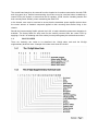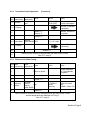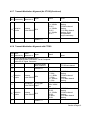
1
PHILIPS
PRM80 SERIES VHF/UHF MOBILE
RADIO TELEPHONE
WARNING
The transistors used in the transmitter power amplifier contain beryllium
oxide, the dust of which Is toxic.
No danger can arise from normal handling, but no attempt should be
made to tamper with the encapsulation of these devices. They must not
be discarded with Industrial or domestic waste.
Publication Ref. 9585 666 80000
Issue B. - November, 1989.
This handbook Is for the maintenance of telecommunication equipment. The performance
figures quoted are typical and are subject to normal manufacturing and service tolerances.
The right Is reserved to alter the equipment or specifications In the light of technical
development.
This publication Is copyright and no part may be reproduced or copied without the prior
permission of Philips Radio Communication Systems (Australia) .
Philips Radio Communication Systems
Box 105, Clayton, Victoria, Australia, 3168. Telephone: (03) 542 4500
Telex: AA20165 (PHILIND) AUSCLTW+ FAX: (03) 543 7935
Printed in
SECTION 1 INTRODUCTION
1.1
PRODUCT DESCRIPTION
Section 1 Page
1
1
TABLE OF CONTENTS
1.1.1
1.1.2
Product Variants
Product Family
1
2
1.2
1.3
1.4
MECHANICAL CONSTRUCTION
SERVICE/ACCESSIBILITY
SALES CODES
3
4
5
1.4.1
1.4.2
The 12-digit Sales Code
The 20-digit Supplementary Technical Code
5
5
1.5
OPERATING INSTRUCTIONS
7
1.5.1
1.5.2
1.5.3
1.5.4
1.5.5
1.5.6
1.5.7
1.5.8
Safety First
Advice to User
Introduction
Common Functions And Facilities
Other Functions
Scanning Functions
Selective Call Facilities
Alert Tones
8
8
9
9
10
12
13
15
1.5.9
Equipment Data Sheet
16
SECTION 2 TECHNICAL SPECIFICATIONS
Section 2 Page
1
2.1
2.2
2.3
2.4
GENERAL
RECEIVER
TRANSMITTER
SIGNALLING
1
3
4
5
2.4.1
PRM80 Selcall Specification
5
2.4.2
PRM80 CTCSS Specification
7
SECTION 3 TECHNICAL DESCRIPTION
Section 3 Page
1
3.1
GENERAL OVERVIEW
1
3.1.1
3.1.2
3.1.3
3.1.4
3.1.5
3.1.6
3.1.7
Receiver
Transmitter
Synthesizer
Microprocessor Control
Signalling
Power Supply and Reset
Controls and Display
2
2
3
3
3
4
4
3.2
DETAILED TECHNICAL DESCRIPTION
5
3.2.1
3.2.2
3.2.3
3.2.4
Receiver
Transmitter
Synthesizer
Central Control
5
8
12
17
3.2.5
Front Panel
26
(i)
SECTION 4 ALIGNMENT PROCEDURE
4.1
TEST EQUIPMENT
4.2
GENERAL INSTRUCTIONS
4.3
PRELIMINARY ADJUSTMENTS
4.4
TEST FREQUENCY TABLE
Section 4 Page
1
1
1
1
2
4.4.1
Selcall Encode Test
3
4.5
THE PROCEDURE
4
4.5.1
4.5.2
4.5.3
4.5.4
4.5.5
4.5.6
4.5.7
4.5.8
VCO Alignment
Transmitter Power Adjustment
Reference Oscillator Tuning
UHF Receiver Front End Alignment
VHF Receiver Front End Alignment
Mute Maximum Alignment
Transmit Modulation Alignment (No CTCSS)
Transmit Modulation Alignment with CTCSS
4
4
5
6
7
8
9
10
4.5.9
Transmit Modulation Alignment with Selcall
11
SECTION 5 INSTALLATION INSTRUCTIONS
5.1
Section 5 Page
GENERAL INFORMATION
1
1
5.1.1
5.1.2
5.1.3
5.1.4
5.1.5
5.1.6
5.1.7
Operator Access
Location Dangers
Vehicles Fitted With Electronic Devices
Specialised Vehicles
Dash Mounted Equipment
Petrol Powered Vehicles
Gas Powered Vehicles
1
1
1
2
2
2
2
5.2
MAIN UNIT FITMENT
3
5.2.1
5.2.2
5.2.3
5.2.4
5.2.5
5.2.6
Cradle Installation
Transceiver Fitment
Transceiver Removal
Microphone Installation
Microphone Removal
Torque Settings for Retaining Screws
3
3
3
3
4
4
5.3
5.4
ANTENNA INSTALLATION
4
DC SUPPLY CONNECTION
SECTION 6 COMPONENT SCHEDULE
4
Section 6 Page
1
6.1
W1 BND, 3Ch, 25kHz STD.
1
6.1.1
6.1.2
6.1.3
6.1.4
Front Panel Assy Compl
Control Brd (std) Compl
Radio Brd W1 25kHz Comp
Common Parts
1
1
4
10
6.2
OPTIONS
10
6.2.1
CTCSS And RTB
10
SECTION 7 DIAGRAMS
7.1
(ii)
List of Illustrations
Section 7 Page
1
1
SECTION 1
1.1
INTRODUCTION
PRODUCT DESCRIPTION
The PRM80 series of mobile radio transceivers are primarily, under dash
mounted local controlled simplex radios, for vehicular application.
The design concept utilises an advanced microcomputer controlled frequency synthesizer.
The microcomputer also performs analogue signalling. The selective calling systems
provided meet the requirements of both standard despatch communications and special
systems applications in world-wide private mobile radio markets.
In addition to the tone sequential signalling, continuous tone controlled squelch system
(CTCSS) signalling is provided and includes the reverse tone burst encode feature.
The customization of the microcomputer control is via an electrically erasable programmable
read only memory (EEPROM). The mobile radio may be configured to meet specific
customer requirements by programming the EEPROM via the data port available at the
microphone socket.
An innovative receiver design provides full band coverage without the need for mechanical
tuning. Similarly, a range of broadband transmitter power amplifiers, offering a selection of
power output levels, provide full band coverage without the need to mechanically re-tune.
The local control front panel is available in two versions. One version provides up to 9
channels and control of a limited set of software programmable options. The other version
provides up to 64 channels, and additional buttons and display indicators give the operator
access to a more comprehensive range of features. Both front panels utilise liquid crystal
displays with permanent backlighting.
The PRM80 is constructed with extensive use of miniature surface mounted components.
The compact electro-mechanical design interconnects the various circuit functions without
the use of point to point wiring, making the PRM80 a true "wireless" radio.
1.1.1
Product Variants
The main unit of the PRM80 transceiver is available in a number of uniquely configured
hardware variants. These variant related items are listed below.
i)
Channel Capacity
9-channel or 64-channel
(Different front panel and memory capacity).
Section 1 Page 1
ii)
Transmitter Power
1 to 6 watt, 1 to 25 watt, 10 to 40 watt.
(Different printed circuit board assemblies required for
each option).
iii)
Frequency Band
EO band, A9 band/BO band, Tm band,
UO band, W 1 band, W4 band.
(Different printed circuit board assemblies required for
each band).
iv)
Channel Spacing
12.5kHz, 20kHz, 25/30kHz.
(Different printed circuit board assemblies required for
each option).
v)
Frequency Stability:
+/-5 ppm -10 to +60 Deg C (Better quality crystal).
+/-10 ppm -10 to +60 Deg C (Standard crystal).
+/-5 ppm -30 to +60 Deg C (Extended temp option).
+/-2.5 ppm -10 to +60 Deg C (TXCO).
+/-2.5 ppm -30 to +60 Deg C (TCXO)
+/-10 ppm -30 to +60 Deg C (Extended temp option)
vi)
Receiver Mute
Adjustable/Preset.
(Additional components required on printed circuit board).
vii)
Signalling
- Without CTCSS encoder/decoder
- With CTCSS encoder/decoder
(Additional components on printed circuit board).
- Standard Selcall
- High performance Selcall
(Additional components on printed circuit board).
viii)
Systems:
- Standard no systems interface
- Systems interface.
(Additional components on printed circuit board).
1.1.2
Product Family
The PRM80 is provided with a family of product related ancillaries for standard vehicular
installation and base or office environment application.
The
ancillaries are:
i)
Desk top housing with mains power supply.
ii)
Stand microphone.
iii)
Boom microphone.
iv)
Hands-free microphone.
v)
Small loudspeaker.
Section 1 Page 2
vi)
Large loudspeaker
vii)
Depot Data programmer.
viii)
24 volt to 12 volt do to do converter.
ix)
Interference filter (12 volt do power).
1.2
MECHANICAL CONSTRUCTION
The main transceiver unit contains three printed circuit boards. Each are double sided epoxy
fibreglass with plated through holes. Extensive use is made of surface mounted components but
conventional leaded components are also used.
The three printed circuit boards are defined as:
i)
FRONT PANEL
ii)
CONTROL
iii)
RADIO
An aluminium diecast chassis provides for heat sinking of the power amplifiers and regulator
devices. The radio and control PCBs are attached to this and are shielded from each other by a
central partition which is part of the main casting. The radio PCB has a separate zinc die cast
shield which is fitted on the component assembly side. This shield effectively compartmentalizes
circuit function areas on the radio PCB. Interconnection between the radio and control PCBs is
via a flexible printed circuit with a zero insertion force socket fitted to the radio PCB.
Interconnection from the control PCB to the front panel PCB is via a flexible printed circuit with a
zero insertion force socket fitted to the front panel PCB. No wiring looms are used in the
mechanical assembly.
A moulded plastic sleeve provides a styling cover over the PCB and chassis assembly. The front
panel PCB is housed in a separate plastic moulding.
In the 9-channel front panel, four moulded plastic buttons are clipped in as part of the front panel
moulding. A clear plastic lens welded to the front panel moulding provides protection for the
liquid crystal display. Behind the LCD is a light diffuser lens to aid in back lighting and location of
the LCD electrical connector (zebra strip). Placed between the front panel moulding and the front
panel PCB is a moulded rubber mat containing the switch contact pads and this mat also aids in
location of the complete LCD/Diffuser/Zebra Strip assembly.
The 64-channel front panel is similar in construction to the 9-channel version, however, 8 buttons
are provided which are clipped into the moulded assembly. The LCD is retained on the front
panel printed circuit board assembly by a pressed metal frame. This frame also retains the
switch rubber mat and LCD diffuser assembly.
The front panel PCBs are attached to the front panel moulding by fixing screws.
Section 1 Page 6
The front panel assembly is attached to the outer sleeve and a dust and water seal gasket is
provided at this interface.
The antenna connection is provided by a chassis mounted BNC type socket at the rear of the
main chassis. Connection to the loud speaker and do power is provided by a 4-way connector
socket mounted on the control PCB, and is accessed at the rear of the main chassis. For special
systems applications, a 15-way 'D' type connector is mounted on the rear of the chassis and
connected internally via a ribbon cable and plug to the control PCB.
The microphone socket is mounted on the control PCB and is accessed via an opening in the
front panel moulding. A clip-on moulded plastic facade covers the microphone socket
connection.
The installation mounting cradle is fixed to the central partition section of the main chassis. Two
fixing screws remain attached to the chassis and secure the outer sleeve in position. The cradle
is secured in position by two more screws. Tilt adjustment of the cradle mounting is set before
the screws are finally tightened.
1.3 SERVICE/ACCESSIBILITY
To gain access to the PCB assemblies the front panel must be detached first (microphone, knob,
one fixing screw, one lock nut and disconnect the flexible printed circuit from the front panel).
The outer sleeve is then removed (four fixing screws). The front panel may be re-attached to the
control PCB with the flexible PCB/socket interconnection. At this level of assembly the equipment
may be operated and aligned. Access to the component side of the control PCB is possible. The
majority of the components on this board are surface mounted and may be serviced with the
PCB in-situ.
To gain access to the radio PCB the radio screen must be detached (nine fixing screws). The
equipment may be operated at this level of assembly but with degraded performance in terms of
case radiation and spurious response and emissions. For service, access to the component side
is possible . The majority of the components on the radio PCB are surface mounted and may be
serviced with the PCB in-situ.
For access to the underside of the radio PCB three fixing screws must be removed, fixing screws
on the transmitter power amplifier devices must also be removed (6 for UHF 25W & 40W, 4 for
the UHF 6W version, 3 for the VHF 6W & 25W, and 5 for the 40W VHF version). The antenna
socket connection must be de-soldered and the 13 volt power connection at the chassis feed
through must be de-soldered. The radio board may then be detached from the chassis but will
remain connected to the control PCB by the flexible interconnecting circuit. This flexible PCB
may be disconnected at the socket on the radio board.
For access to the underside of the control PCB the front panel must be detached. The
microphone must also be removed. The control PCB is retained by six fixing screws, the audio
amplifier IC and two regulator ICs are attached to the chassis by four fixing screws which must
be removed. The 13 volt power connection at the chassis feed through must be de-soldered.
Section 7 Page 4
The control board may then be removed from the chassis but it remains connected to the radio PCB
and front panel by a flexible interconnecting circuit-Care must be exercised when re-attaching a
control PCB to the chassis, to ensure that the 5V regulator, IC208, has the insulating washer and
bush correctly fitted. Similarly, when re-attaching the radio PCB
to the chassis, care must be exercised to ensure that the transmitter power amplifier devices have
the correct amount of heatsink compound applied to their mounting faces before fixing to the
chassis.
Should the interconnecting flexible printed circuit fail, a hand solderable replacement alternative is
available. The factory fitted flex strip must first be carefully removed from the control PCB, by
applying a "hot air" de-soldering tool to the solder joint and peeling away the soldered connections.
1.4
SALES CODES
There are, basically, two codes to be described; the 12-digit sales code and the 20-digit
supplementary technical code. A sample of this latter code sheet is included.
3
1.2
Provisi Chann
el
onal
Spacin
7
2
3
4
6
B
7
6
9
4,5
7
10
11
15
6
12
14
8
9
13
Freq Freq. RF
CTCS Seque Installa
Speak Noise
Control Version
Mic.
Band Stab Power
S
nt.
tion
er Blanke
(MHz)
(Watts)
Signall
Signalli
Not
Not Notr
Not
Not
No kit.
require require fittedfitted. fitted.
d. Stand
d.
5pp 1 to
SPRM8
Selcall Swivel Stand
LocalENC.
Fitted.
m
25
12.5
010.
ENC bracke ardard-T0 (Std2.5p
1 to
E0 PRM6 ENC/ Selcall t
Comp
R - 20
Stick.
25
68-88 p020. DEC. ENC(
act.
80.
1opp T T0
ENC/
V - 25
DTMF.
132m
6
DEC
I56 -T0
to 10T04
(Low
plus
A9
2.5pp
ENC/
X - 30
1445m 0
DEC
T74
30
plus
TM5ppto (High
400m
Lo lopp
440m
470
470- -30 to
500
W4
500 520
16
Equip
ment
Label
Philips
.
None
fitted.
17
Power
Switch
Stand
ard
conne
Bypas
sed
for
18
Syste
ms
Not
fitted.
Fitted.
19
20
Mute Provisional
Variab
le.
I
Fixed-
1.5.1
1.
Safety First
The use of the mobile radio while driving may be in breach of traffic regulations in
some countries. Check with your local Traffic Authority for further details.
Please do not use a hand-held microphone while you are driving.
2.
DO NOT operate the mobile radio in an explosive atmosphere.
Obey the "Turn Off TWo Way Radios" signs where these are posted.
3.
To avoid radio frequency injury, DO NOT TOUCH THE ANTENNA whilst
the mobile radio is in use.
4.
A possibility exists, based on isolated incidents in the past, that the use of a mobile
radio in your vehicle may result in the altered operation of electronic systems
(eg. fuel injection and braking systems).
If this occurs:- TURN OFF Your Mobile Radio IMMEDIATELY, and contact your Sales
Representative for advice.
5.
1.5.2
Fans, power accessories, window demisters or radios may alter the operation of your
mobile radio. Consult the accessory manufacturer for details regarding the elimination
of radio interference from such accessories.
Advice to User
1.
Only transmit when the channel is free.
2.
Do not speak while you can hear a tone sequence coming from the loudspeaker.
3.
Hold the microphone 2 to 3 centimetres from your mouth and speak across it.
4.
Do not occupy the channel any longer than is necessary.
5.
Replace the microphone after use.
6.
Identify yourself using your allocated radio identity.
7.
Restrict the length of messages.
8.
Avoid making calls from known poor signal areas such as the radio system's fringe
areas or from screened areas, eg. an underground car park or underpass.
Section1 Page 11
1.5.3
Introduction
The Type PRM8010 transceiver is a versatile, microprocessor-controlled, dash-mounted, mobile
radio designed to access facilities provided by the Private Mobile Radio Service.
The transceiver is software programmable to produce the options required to suit specific
requirements. Though many options are available, each unit is dispatched from the factory
programmed with a specific software application package, so that only a few parameters need to
be varied in the field (eg. frequencies, selective call identities).
This guide describes all the facilities that are currently available, though some may not be
available on your equipment.
The facilities that are available to you are most easily identified by examining the key label
overlay on the front panel display.
Common functions and facilities are described in section 1.5.4.
Other functions are described in section 1.5.5.
Scanning functions are described in section 1.5.6.
Selcall functions are described in section 1.5.7.
Some specially adapted application packages may include facilities described separately in
supplementary information sheets.
1.5.4
Common Functions And Facilities
1.5.4.1
SWITCH ON/OFF
To switch on, press the On/Off switch.
The LCD (Liquid Crystal Display) backlighting will be on when power is connected to the set.
To switch off, press the On/Off switch.
If the radio is wired for external on/off switching the On/Off switch will control only the display.
The radio will be automatically switched on and off via external switching circuit.
1.5.4.2
SPEECH RECEPTION
Select the required channel by using 'Channel UP' button.
Pressing this button enables the selection of higher numbered channels, returning to
the lowest channel number once the highest number has overflowed.
Set the 'squelch' control fully anti-clockwise.
In the absence of a signal the squelch control eliminates receiver noise and also
suppresses weak interfering signals.
Section 1 Page 9
Adjust the 'volume' control until receiver noise is heard.
The volume control adjusts the speech level at the loudspeaker. Clockwise
rotation increases the volume, anti-clockwise rotation decreases the volume.
Turn 'squelch' control clockwise just until the receiver noise disappears.
Note that this is the most sensitive setting of the squelch control. Turning the squelch
control further clockwise will suppress weak interfering signals.
If the receiver is fitted with a 'fixed squelch' then the volume control is used as
normal to obtain a suitable audio level when speech is being received.
If the radio is fitted with a 'squelch defeat' switch, this button may be used when
operating in very weak signal areas.
1.5.4.3
SPEECH TRANSMISSION
To avoid interfering with other users of the operating channel, listen first to ensure that no
transmissions are being made.
Make sure that the 'Busy' indicator is OFF.
Holding the microphone 2 to 3 centimetres from the lips, press the 'press-to-talk' switch (on the
microphone) and note that the transmit indicator is turned ON. Speak clearly across the face of
the microphone in a normal conversational manner.
Use the correct operating procedure, and keep transmissions short. Release 'press-to-talk'
switch as soon as the message is finished and note that the transmit indicator is turned OFF.
When the 'transmit limit timer' option is fitted the transmitter will be turned off at
the end of preset time, and a warning signal (if programmed) will be heard until
the 'press-to-talk' switch is released. Re-pressing the 'press-to-talk' switch will
turn on the transmitter.
If the 'transmit inhibit' option is fitted transmission will not be possible while a
signal is being received, as indicated by the Busy Indicator.
1.5.5
Other Functions
This section deals with mobile facilities that are not apparent from the front panel of the
transceiver, but which may significantly affect the operation of the transceiver.
These facilities are usually specially configured and require special operating practices which will
be explained by your system controller or in supplementary information sheets. If you are unsure of
how your equipment is configured with respect to these facilities you should contact your supplier.
1.5.5.1
TRANSMIT INHIBIT
If your equipment has the transmit inhibit facility programmed, you will be prohibited from
transmitting either with the 'press-to-talk' switch or with any 'Send' button whenever the radio
channel is busy and the 'Busy' indicator is on.
Section 1 Page 13
If the equipment is fitted with CTCSS and/or selective calling, the busy indicator and the transmit
inhibit facility are both defeated whenever a valid call is received, so that you can respond to the
call.
1.5.5.2
TRANSMIT LIMIT TIMER
The transmit limit timer limits the duration of the transmission. The transmission time may be set,
in steps of one second, from 1 to 255 seconds. On expiry of the timer the transmission will cease
and a continuous audible alarm will sound while the PTT switch is held pressed. To re-initiate
the transmission the PTT switch must be released and then pressed.
1.5.5.3
TRANSMIT RE-PTT TIMER
The transmit re-PTT timer limits the minimum time between the release of the PTT switch, and
the pressing of the PTT switch for the next transmission. The minimum time may be set, in
steps of one second, from 1 to 255 seconds. If the switch is pressed during this time a
continuous audible alarm will sound while the PTT switch is held pressed.
1.5.5.4
TRANSMITTER/RECEIVER LOCKOUT
These facilities are usually programmed together and only on carefully controlled 'closed'
radio systems. On such systems users are prevented from listening to the channel.
1.5.5.5
CTCSS (CONTINUOUS TONE CONTROLLED SQUELCH SYSTEM)
When CTCSS encode only is fitted a sub-audio tone accompanies every mobile transmission.
If the CTCSS decode is supplied, no communication will be heard unless the incoming
transmission contains the correct CTCSS tone.
CTCSS decode can be bypassed by any of the following (if programmed):Removing the microphone from its cradle.
By enabling the monitor button.
1.5.5.6
MICROPHONE CRADLE OPERATION
Depending of the options programmed, the cradle can affect the operation of the transceiver in
any of the following ways:
Mobile may transmit Automatic Number identification whenever the microphone is
removed from its cradle.
Mobile may enter Monitor mode whenever the microphone is removed
from its cradle. Calls may be reset whenever the microphone is returned
to its cradle.
Scanning will only be active if the microphone is in its cradle.
If the microphone is removed from its cradle while the scan has stopped on a
channel, that channel will remain selected until the microphone is returned to its
cradle.
Section 1 Page 14
If the microphone is removed from its cradle while the transceiver is still
scanning, the priority channel will be selected. The channel display will
1.5.6
Scanning Functions
When fitted this option allows a mobile to scan a number of radio channels for a valid signal.
There can be up to 9 channels in a scan group and one of these can be designated as a Priority
channel. This channel will differ from the basic channels in the following:
If there is a priority channel programmed, the radio will check the priority
channel for the presence of a signal in between normal channels.
If the microphone is removed from its cradle while the transceiver is still
scanning, the priority channel will be selected and the Channel Display will
While on a scan channel, mobile will still check the pr iority channel for the
presence of a valid signal until the microphone is removed from its cradle.
Scanning will only be active if the microphone is in its cradle (ie. on hook).
1.5.6.1 OPERATION
To enter Scan mode press the SCAN
button.
The Scan chevron will turn ON. The Channel display will be
blanked and the SCAN indicator will start flashing.
If the error tones sound when the SCAN button is pressed, it will
mean that:
the scan group is empty, or
the current channel is not allowed as a priority priority channel, or
the 'press-to-talk' switch is currently pressed.
The radio will scan the selected channels in sequence. The scan will continue until a valid
signal is found.
When a valid signal is found the mobile will halt scanning, the 'Scan'
indicator will cease flashing to become steady, and the channel display
will show the channel number selected. .
Remove the microphone from its cradle.
This channel will remain selected until the microphone is returned to its cradle and
scanning resumes.
Terminate the scan mode by pressing the 'Scan' button.
Section 1 Page 15
The mobile will return to the channel that was selected before the scan function was initiated.
1.5.6.2
SELECTION OF PRIORITY CHANNEL (if enabled)
Select the required channel by using 'Channel UP' button.
Use the 'SCAN' button to initiate scanning.
The channel selected will automatically become the priority channel.
Note: The 'ERROR TONE' will sound if the channel that is selected
is not permitted as a scan channel.
1.5.7
Selective Call Facilities
Selective call is an optional fitting which can allow the mobile radio to respond to, and/or initiate a
signal carrying an identifying number.
A number of different operations are available depending on the system configuration and the
features programmed.
The facilities currently available are indicated below. Please note that some of these may not be
available on your equipment.
1.5.7.1
SEND 1
The Send button causes a programmed identity to be transmitted. This identity is used to identify
the mobile to the base control.
1.5.7.2
SEND 2
Used as Send 1 but provides for a second identity.
1.5.7.3
ALARM
Alarm is a special version of Send. It is used to indicate the presence of an alarm condition or it
can be used as a priority call request. The exact use of this function will depend upon how your
particular radio system has been designed. You should have specific instructions about when this
button is to be used.
Please note that the mobile radio is controlled by the base controller during the
emergency mode.
Alarm may also be activated by a special switch (if fitted),external to the
equipment.
Alarm condition can be reset from base control, or by disconnecting the radio
from the battery.
Section 1 Page 13
1.5.7.4
EXTERNAL ALERT
This button is used to control an external device, such as the vehicle horn. It is normally switched
on when you expect to be outside your vehicle and it will be activated, whenever your equipment
receives a valid call.
1.5.7.5
MONITOR / RESET
This button can be programmed to enable you to listen to all calls on the channel. It can be toggled
between the quiet and listen modes.
This button also cancels the called indicator.
1.5.7.6
RESET
In closed systems, the mobile is allowed to listen to a voice channel only when it receives a valid
selcall from the base control. The Reset button allows the mobile to revert to quiet mode. When
used it cancels the called indicator.
1.5.7.7
TRANSPOND
Transpond provides a facility for the mobile to automatically transmit a predefined identity to
acknowledge that a call has been received. This switch is used to enable/disable this facility.
1.5.7.8
SELCALL RECEPTION
Whenever a valid call is received the equipment will display the 'Call' indicator. It will also sound the
appropriate call alert.
You may answer the call by operating the 'press-to-talk' switch. The indicator and alert tone will be
cancelled. Additionally, if programmed, removing the microphone from its cradle will cancel the
indicator and alert tone. Alternatively the call may be cancelled by pressing the monitor button once.
If you do not answer the call, the call alert will stop after a few seconds but the indicator will remain
on. Depending on how your radio system is configured, the call can be terminated in one of the
following ways:
Removing the microphone from its cradle.
Pressing the 'Monitor' button once.
By receipt of 'Remote Reset' signal from the base
control. By expiry of the 'timed reset timer'.
By returning the microphone to its cradle.
Section 1 Page 14
1.5.8
Alert Tones
The frequency of all 'alert tones' is 500Hz.
TYPE OF ALERT
ERROR
Generated when operator
TONE presses an invalid button.
_2
CONTINUO Generated on Invalid
TONE
of PTT, or If microphone left
ERROR of cradle
3
KEY
BEEP
TONE
Generated when any button Is
pressed.
4
DECODE 1 Generated for selcall decode
ALERT
response.
TONE
5
URGENT
ALERT
TONE
Generated for selcall urgent
response.
6
GROUP
ALERT
TONE
Generated for selcall group
response.
NORMAL
DECODE
ALERT
TONE
Generated for selcall normal
response.
Section 1 Page 15
1.5.9
Equipment Data Sheet
An individual data sheet listing all transmitter and receiver frequencies, including
signalling information, is supplied with each transceiver. It is important that this data
sheet is retained for future use such as the equipment requiring repair or change to
parameters (eg. channels or identities). A sample data sheet is shown below.
Serial Number
200001
Hardware 12NC
9525 001 10072
Application Code
Frequency Band
470 - 500MHz
Encode Signalling
Options
Encode Type
Identity
Individual Identity (1)
53454
Individual Identity (2)
45554
Individual Identity (3)
45453
Emergency Identity
45345
Emergency Identity
45435
Individual Call
45345
Encode Tone Set
CML CCIR
Lead in Delay
mSec
Lead out Delay
msec
Decode Signalling
Options
Indiv Decode Identity
45345
Group Decode
435345
Reset Decode Identity
43534534
Decode Tone Period
Decode Tone Set
Tone Period
l00ms
l00ms
l00ms
l00ms
looms
looms
600
100
l00ms
CIVIL CCIR
Scan Group Selection
Is Selectable Priority
PriorityRequired
Channel
Channels in Scan
Channel Table
Rx
Ch
Freq
Lock
1
471.0000
No
3
475.0000
No
4 476.0000
Yes
5
477.0000
No
7
480.0000
No
9
495.0000
No
No
3
14679
CTCSS
Freq
471.0000
TX
Lock
No
478.0000
481.0000
Yes
No
CTC/ Selc Co
Yes
No
No
No
No
No
Yes
No
No
No
No
Scan
Yes
Yes
Yes
No
Yes
Yes Yes
Power
High
High
High
High
High
High
Section 1 Page 16
SECTION 2
TECHNICAL SPECIFICATIONS
Unless otherwise stated, specifications apply for an ambient temperature of 25 Deg C and
13.8V supply.
2.1
GENERAL
Operation
Single- or two-frequency simplex.
Modulation
Frequency.
Supply Voltage
10.8V to 16.2V dc, negative earthed to chassis.
Frequency Bands
VHF
UHF
E0 68 - 88 MHz
B0 132 - 156 MHz
A9 146 - 174 MHz
Tm 400 - 440 MHz
U0 440 - 470 MHz
W 1 470 - 500 MHz
W4 500 - 520 MHz
Channel Spacing
VHF
UHF
12.5 kHz
20 kHz
25/30 kHz
12.5 kHz
20 kHz
25 kHz
Frequency Stability
UHF & VHF (option)
crystal).
VHF
crystal).
VHF & UHF (USA)
option).
UHF
UHF
VHF
option)
+/-5ppm
-10 Deg C
to
+60 Deg C (better quality
+/-10ppm
-10 Deg C
to
+60 Deg C (standard
+/-5ppm
-30 Deg C
to
+60 Deg C (extended temp
+/-2.5ppm
+/-2.5ppm
+/-10ppm
-10 Deg C
-30 Deg C
-30 Deg C
to
to
to
+60 Deg C (TCXO).
+60 Deg C (TCXO).
+60 Deg C (extended temp
Section 2 Page 1
Switching Bandwidth
Frequency band coverage without retuning
UHF
VHF
VHF
TM 40MHz, U0 30MHz, W 1 30MHz, W4 20MHz
A9/B0 band 30MHz
E0 band 20MHz
Channel Capacity
i) 9-channel
ii) 64-channel Current Consumption
VHF
Off state
Rx standby
(no AF output)
Tx (25W)
UHF
less than 10mA
less than 10mA
less than 350mA
less than 350mA
less than 5.5A
less than 6.5A
Type Approval Compliance
The PMR80 is designed to comply with the following regulatory specification standards.
i)
Australian DOC
RB206, RB207, RB234B
ii)
New Zealand
RTA25
III)
Canada
RS119
iv)
European
CEPT TR24-01 Annex 1,2,5,7
MPT 1306, MPT 1316, MPT 1326.
RS 15213, RS204C. (Does not comply with squelch
v)
EIA
sensitivity
vi)
FTZ
17.0, or Temp range 22.0).
A446 82023, AA446 82024.
Dimensions
Length;
Width;
Height;
Weight;
203mm (210mm including Volume knob). 160mm.
160mm.
45mm.
less than 1.4kg (including cradle).
Section 2 Page 2
2.2
RECEIVER
Sensitivity
12dB sinad for less than 0.31uV pd. at the antenna socket, for 1 kHz at 60% maximum
deviation and 50% rated AF output power.
Adjacent Channel Selectivity
i).
DOC method
VHF Greater than 4.1mV pd (73dB wrt 0.31uV).
UHF Greater than 5 mV pd (74dB wrt 0.31uV).
Intermodulation Rejection Ratio
Three generator method, greater than 75dB at 100200kHz above and below carrier to avoid
selectivity limitations.
Spurious Response Rejection Ratio
i)
VHF
Greater than 85dB with a single signal.
ii)
UHF
Greater than 80dB with a single signal.
Blocking
Greater than 93dB ratio at 150kHz offset, 2-generator method.
Modulation Acceptance Bandwidth
i)
ii)
iii)
12.5 kHz channel spacing, greater than +/-4kHz.
20
kHz channel spacing, greater than +/-7.0kHz.
25/30kHz channel spacing, greater than +/-8.5kHz.
Spurious Radiation
9kHz to 1GHz less than 2 nW.
1GHz to 4GHz less than 20 nW.
AF Regulation
Less than 1dB variation in AF level for RF input level change from 0.3uV to 100mV PD.
Residual Hum and Noise
channel spacing
12.5kHz
25/30kHz
VHF
41dB
47dB
UHF
40dB
46dB
Reference 1 kHz at 60% deviation. 1 mV RF level. CCITT weighted. CTCSS not fitted.
Section 2 Page 3
Audio Frequency Response
Measured at the loud speaker for a constant deviation at 20% of maximum.
Within +l dB to -3dB of -6dB per octave de-emphasis relative to 1 kHz over 300Hz to 3000Hz,
CTCSS not fitted.
With CTCSS fitted within +1.5 to -3dB.
Audio Output
i)
4 watts into 4 ohms, less than 10% THD with 1kHz at 60% maximum deviation.
ii)
16 watts into 4 ohms, optional.
Audio Distortion
Less than 5% THD for 300mW into 4 ohms, 1kHz at 60% deviation.
Mute Response Time
Mute set to open at 20dB SINAD.
Response for 1 uV RF level; less than 40mSec.
Mute Range
Channel Spacing
12.5kHz
25kHz
maximum
Minimum
18 to 20dB
l0dB
20 to 25dB SINAD.
l0dB SINAD.
2.3
TRANSMITTER
Power Output
Adjustable; 1 to 6 watt, 1 to 25 watt, 10 to 40 watt.
Spurious Emission
Less than 0.25uW 100kHz to 1GHz, less than 1uW 1GHz to 4GHz.
Residual Hum and Noise
Greater than 40dB (Reference 1 kHz at 60% deviation. DC to 25kHz bandwidth CCITT
weighted and 6dB/octave de-emphasis).
Microphone Sensitivity
Less than 20mV rms at 1 kHz to achieve 60% maximum deviation. Standard sensitivity
setting, 40mV +/-10%; Optional setting, 5mV
Audio Distortion
Less than 3%. Reference 1kHz at 60% deviation.
Section 2 Page 4
Audio Frequency Response
i)
25kHz Channel Spacing.
Within +1 to -3dB of a +6dB per octave pre-emphasis, over 300 to 3000Hz (without
CTCSS).
With CTCSS, within +1.5 to -3dB.
ii)
12.5kHz Channel Spacing.
Within +1 to -3dB over 300 to 2550Hz (without CTCSS).
Within +1.5 to -3dB over 300 to 2550Hz (with CTCSS).
Transmitter Rise Time
Less than 40mSec from operation of the PTT to achieve 70% of output power.
2.4 SIGNALLING
2.4.1
2.4.1.1
(i)
over
PRM80 Selcall Specification
ENCODER
Tone Deviation.
Factory preset to 80% or system deviation adjustment range typically 33% to
100% of system deviation.
(ii)
Tone Distortion.
Not greater than 10% at TX VCO input.
(iii)
Tone Frequency Range.
63 possible tones in the range 459Hz to 2937Hz. See Table 2.2 for details.
(iv)
Tone Amplitude Variation.
Not greater than 6dB over 459Hz to 2937Hz.
(v)
Tone Frequency Error.
Not greater than 1.0% -30C to +60C.
(vi)
Tone Period.
14 possible durations from 20 to 255mSec. Accuracy greater than 3.0%. The
required
tone period may be selected from the following:
a)
20 mSec.
b)
33 mSec.
c)
40 mSec.
d)
60 mSec.
e)
70 mSec.
f)
80 mSec.
g)
100 mSec.
h)
120 mSec.
i)
140 mSec.
j)
150 mSec.
k)
200 mSec.
1)
210 mSec.
m)
250 mSec.
n)
255 mSec.
Section 2 Page 5
(vii) Lead-in-Delay.
0 to 65Sec. Accuracy greater than 1%.
(viii) Lead-out-Delay.
0 to 255mSec. Accuracy greater than +0, -1 mSec.
(ix)Send Repeat Rate.
Approx 100mSec following end of transmission. Additional send keystrokes are
ignored during
encode.
(x)Code Formats.
Up to 10 tones per sequence.
2.4.1.2
(i)
Decoder
Sinad Sensitivity.
For 90% decode success rate sinad is measured at speaker output.
1.
2
(ii)
Standard Selcall.
20mSec
40mSec
l00msec
255mSec
14dB Sinad
15dB Sinad
13dB Sinad
l4dB Sinad
Enhanced Selcall.
20mSec TBA
40mSec TBA
100mSec TBA
255mSec TBA
Deviation Sensitivity.
Minimum deviation for 90% success rate and full receiver quieting.
1
Standard selcall.
Less than 0.3kHz deviation.
2.
Enhanced selcall.
TBA.
(iii) Decode Bandwidth.
80% deviation and full quieting.
CCIR 1.5% to 3 %
ZVEI 2.0% to 4.5%
EEA 1.5 % to 3.5 %
EIA
1.5 % to 3.5 %
DZVEI 2.0% to 4.5%
NATEL1.3% to 1.7%
Section 2 Page 6
(iv)
Valid Tone Period for Successful Decode.
80% deviation and full quieting.
-40% to +70%
(v)
Code Format.
A successful decode will occur if the correct code address is preceded with
and/or
followed by
erroneous tones or noise.
(vi)
Decode Recognition.
Upon receipt of correct decode address, no action occurs (ie mute open, auto
acknowledge, etc) until approximately one tone period has elapsed.
2.4.2
PRM80 CTCSS Specification
2.4.2.1
Encoder
(i)
Tone Deviation.
25kHz channel spacing
500 to 700Hz.
20kHz channel spacing
400 to 560Hz.
12.5kHz channel spacing
250 to 350Hz.
7% to 36% of systems deviation adjustment range.
(ii)
Tone Distortion.
Less than 5.0%.
(iii)
Frequency Accuracy.
+/- 0.30% over -30 degC to +60 degC.
(iv)
Number of Tones.
There are, including disabled, 38 available tones. See Table 2.1.
2.4.2.2
Reverse Tone Burst.
In order to prevent the mute "tail" associated with the de-response time of CTCSS decoders,
the mobile may be equipped with reverse tone burst (RTB). This RTB, occurs at the end of
CTCSS transmission and consists of a period of CTCSS tone of either 180 or -120 degrees
phase difference to that previously sent. The period of this tone is dependent on the tone
frequency, see Table 2.1.
The RTB installation may be either hardware or software.
(i)
Hardware RTB.
RTB phase Shift:
120 degrees +/- 10 degrees, lagging.
RTB duration:
Between 80mSec to 150mSec.
CTCSS tone frequency dependent. See Table 2.1.
RTB Amplitude Variation
+/- 2dB.
(across CTCSS tone set).
Section 2 Page 7
(ii)
Software RTB.
RTB phase shift:
RTB duration:
RTB amplitude variation
(across CTCSS tone set).
2.4.2.3
180 degrees +/- 10 degrees, lagging.
between 80mSec to 150mSec.
CTCSS tone frequency dependent. See Table 2.1
0.5dB.
Decoder
(i)
Tone-Set.
as per Encoder.
(ii)
Bandwidth.
+/- 3.0% max.
(iii)
Deviation Sensitivity.
Better than 6% of system deviation (for decode with full RF quieting).
(iv)
Noise Immunity.
Less than 500mSec dropout per minute for l0dB sinad
(CTCSS tone deviation 10% of system and sinad signal of 60% deviation at
1kHz).
(v)
False Decode Rate.
Less than 5 false decodes per minute (no carrier input).
(vi)
Talkoff.
I
nterfering tone deviation for loss of decode (CTCSS tone deviation 10% of
system).
Full quieting RF signal:
dropouts).
310Hz to 3kHz 90% of system deviation (for no
20dB sinad RF signal:
dropouts in one
12dB sinad RF signal:
320Hz to 3kHz ; 90% of system deviation (for no
minute).
350Hz to 3kHz; 90% of system deviation (for no dropouts
in one minute).
(vii)
deviation;
Less than 250mSec.
(With a full quieting signal of 67Hz at 10% of system
67Hz gives the slowest times).
(viii)
Less than 250mSec.
Response Time;
De-response time;
2.4.2.4
Speech Rejection Filter
(i) Response.
300 Hz 0 dB.
250 Hz <-36 dB.
Section 2 Page 8
Table 2.1 CTCSS Tonesets Available In the PRM80
FREQ. (Hz)
Tone Number
R.T.B. Duration
(mSec)
(disabled)
67.0Hz
71.9 Hz
74.4 Hz
77.0 Hz
79.7 Hz
82.5 Hz
85.4 Hz
88.5 Hz
91.5 Hz
94.8 Hz
97.4 Hz
100.0 Hz
103.5 Hz
107.2 Hz
110.9 Hz
114.8 Hz
118.8 Hz
123.0 Hz
127.3 Hz
131.8 Hz
136.5 Hz
141.3 Hz
146.2 Hz
151.4 Hz
156.7 Hz
162.2 Hz
167.9 Hz
173.8 Hz
179.9 Hz
186.2 Hz
192.8 Hz
203.5 Hz
210.7 Hz
218.1 Hz
225.7 Hz
233.6 Hz
241.8 Hz
250.3 Hz
00
17
18
19
20
21
09
22
01
23
10
38
02
11
03
12
04
13
05
14
06
15
07
16
08
24
25
26
27
28
29
30
31
32
33
34
35
36
37
---150
140
140
140
130
130
130
130
120
120
120
120
120
110
110
110
110
110
110
110
110
110
110
110
110
90
90
90
90
90
90
90
80
80
80
80
80
80
Section 2 Page 9
TABLE 2.2 Selcall Tonesets Available In the PRM80
TONE
#
0
1
2
3
4
5
6
7
8
9
A
B
C
D
E
F
TONE
#
Manucturer s
Type N
International
System No.-
.
Manufacturer's
Type No.Intematonal
System No.
0
1
2
3
4
5
6
7
8
9
A
B
C
D
E
F
TONE
#
0
1
2
3
4
5
8
7
8
9
A
B
C
D
E
F
Manufacture's
Type No. -+
Intemadonal I
System No.
CML
ST-500 SIG TEC SIG TEC SEPAC
CML
ST-500 0 SIG TEC
CCIR
CCIR
CCIR
CCIRH
CCIR
EEA
EEA
EEA
1981
1124
1197
1275
1358
1448
1540
1640
1747
1860
2400
930
2247
991
2110
------
1981
1124
1197
1275
1358
1446
1540
1640
1747
1860
------1055
2400
------2110
-------
1981
1124
1197
1275
1358
1446
1540
1640
1747
1860
2110
2400
1055
2247
930
991
1981
1124
1197
1275
1358
1448
1560
1640
1747
1860
2400
930
2247
991
2110
1055
1981
1124
1197
1275
1358
1448
1540
1640
1747
1860
2400
1055
2247
991
2110
-----
1981
1124
1197
1275
1358
1448
1540
1640
1747
1860
1055
930
2247
991
2110
-----
1981
1124
1197
1275
1358
1446
1540
1640
1747
1860
1055
------2400
------2110
-------
1981
1124
1197
1275
1358
1446
1540
1640
1747
1860
2110
1055
2400
2247
930
991
SEPAC CML
ST-500 'SIGTEC
SEPAC
SIGTEC
SEPAC
SIGTEC
EEA
ZVEI
ZVEI
ZVEI-1
ZVEI-1
ZVEI-2
ZVEI-2
ZVEI-3
1981
1124
1197
1275
1358
1446
1540
1640
1747
1880
1055
970
2247
2400
2110
-------
2400
1060
1160
1270
1400
1530
1670
1830
2000
2200
2800
810
970
886
2600
------|
2400
1060
1160
1270
1400
1530
1670
1830
2000
2200
970
------2800
------2600
-------
2400
!1060
1160
1270
1400
1530
1870
11830
2000
2200
2900
2800
741
970
810
886
2400
1060
1160
1270
1400
1530
1670
1830
2000
2200
2800
970
885
------2600
-------
2400
1080
1160
1270
1400
1530
1670
1830
2000
2200
970
885
741
2600
2800
600
2400
1060
1160
1270
1400
1530
1670
1830
2000
2200
885
741
2600
------970
-------
2200
970
1060
1160
1270
1400
1530
1670
1830
2000
2400
885
741
2600
2800
600
SEPAC ST-500 ST-500 ST-500
\CML
\CML
SIGTEC
SIGTEC
SEPAC
ST-500
ZVEI-3
ZVEI-3
DZVEI
DZVEI
NATEL
EIA
EIA
EIA
2200
970
1060
1160
1270
1400
1530
1670
1830
2000
885
741
2600
------2400
--------
2400
1060
1160
1270
1400
1530
1870
1830
2000
2200
885
------810
------970
--------
j2200
970
1080
1180
1270
1400
1530
1670
1830
2000
2600
------886
810
2400
-------
2200
970
1060
1160
1270
1400
1530
1670
1830
2000
825
------2600
------2400
-------
1633
631
697
770
852
941
1040
1209
1336
1477
1805
1995
1300
1700
2175
2937
600
741
882
1023
1164
1305
1446
1587
1728
1869
459
2151
2600
2010
2433
2292
600
741
882
1023
1164
1305
1446
1587
1728
1869
2151
1091
2400
------459
-------
600
741
882
1023
1164
1305
1446
1587
1728
1869
2151
------2010
------459
--------
SECTION 3
3.1
TECHNICAL DESCRIPTION
GENERAL OVERVIEW
Shown in figure 3.1 is the overall simplified block diagram of the PRM80.
Figure 3.1
PRM80 - Overall Block Diagram
The transceiver consists of three printed circuit board assemblies.
i)
Front Panel Board
Containing the liquid crystal display, its driving circuit, push button switches and
display backlighting.
ii)
Control Board
Containing the microprocessor with its associated clock and latches, EEPROM
memory, power supply and reset circuit, transmitter audio processing, receiver
audio processing, selective call audio processing and CTCSS signalling option.
Section 3 Page 1
iii)
Radio Board
Containing the transmitter power amplifier with antenna switch, receiver front end filters and
mixer, receiver IF and demodulator, synthesizer and reference oscillator, transmit and receive
voltage controlled oscillators, and transmitter audio low pass filter. All the frequency band and
channel spacing related components are on this board assembly.
3.1.1
Receiver
The receiver concept utilizes a double conversion superhetrodyne principle with first and
second intermediate frequencies of 21.4 MHz and 455kHz respectively.
The front end of the receiver uses electronically tuned bandpass filters and a radio frequency
amplifier ahead of a double balanced mixer. The frequency conversion to the first IF of
21.4MHz occurs in this mixer with the local oscillator injection from the receive voltage
controlled oscillator. Monolithic crystal filters at 21.4MHz provide the first stage of adjacent
channel rejection. Amplification at 21 4MHz is provided ahead of the frequency conversion to
the second IF of 455kHz. The final stage of adjacent channel rejection is provided by a
ceramic filter.
The second conversion, IF limiter amplification and FM demodulation are all processed in a
single integrated circuit. The demodulated audio out of this IC is first low pass filtered to
remove residual 455kHz products and then further audio frequency processing, such as
300Hz to 3000Hz band pass filter and de-emphasis, is provided. The mute gate is placed
before the volume control adjustment, which is ahead of the audio power amplifier.
The demodulated output is also high pass filtered, amplified and detected. The quieting of the
detected noise provides for mute control.
3.1.2
Transmitter
The transmitter power amplifier line up, amplifies the signal output of the transmit voltage
controlled oscillator, which is at the final carrier frequency. The amplification is sufficient to
achieve 25 watts final output from the nominal 20 milliwatt level of the VCO.
The amplifier design is broadband without mechanical tuning. Power output is stabilized by the
action of a feedback loop. This power control loop circuit also protects the amplifier from
excessive load mismatch conditions and temperature rise. The output from the amplifier is
coupled to the antenna socket via the antenna change over switch and the harmonic rejection
low pass filter.
Power output may be set between 1 watt and 25 watts, with the option of switching between
two preset power levels. An RF output detector is monitored so that in the presence of RF
power the transmit indicator is illuminated.
Transmit audio processing begins with an active microphone containing a transistor preamplifier. In the transceiver unit the microphone signal is filtered and amplified, ahead of
Section 3 Page 2
an amplitude limiter stage. Following the limiter the signal is low pass filtered prior to
modulating the transmit VCO. Provision is made to combine microphone and signalling audio.
3.1.3
Synthesizer
The frequency synthesizer provides the functions of excitation for the transmitter power
amplifier, and the receiver first local oscillator. A single phase locked loop principle is used
with synthesis at the required final frequency. The phase locked loop comprises the transmit
and receive VCOs, a prescaler/divider, programmable divider and phase comparator,
reference oscillator,and loop low pass filter. The action of the loop is to phase lock the VCO
frequency to the stable reference frequency which is derived from a crystal oscillator.
The synthesizer is reprogrammed to a new frequency by a serial sequence of data commands
to the programmable divider IC, this data is latched in the IC. For frequency modulation in
transmit mode, both the transmit VCO and the synthesizer reference oscillator have
modulation applied.
3.1.4
Microprocessor Control
A single chip 8-bit CMOS microprocessor forms the basis of the computer control circuitry.
Within this device is a masked program read only memory. This program performs the
generation and detection of selective call tone sequential signalling, as well as the operational
characteristics of the selcall system response. In addition to this, other major functions include
programming of the synthesizer, controlling the display of LCD information, controlling the
receiver audio mute and transmit microphone mute, monitoring the front panel
buttons,controlling CTCSS and reverse tone burst signalling, and performing the task of
programming and reading the electrically erasable memory.
The electrically erasable memory contains the user customizable information, which includes
features such as channel frequency, signalling system requirement (toneset, code, system
response etc.), transmit limit timer value. This memory is programmed or read via the
microprocessor, from the microphone socket interface.
The microprocessor operates from an external 1'6MHz clock using a crystal oscillator. This
clock frequency is divided by an additional IC to provide a clock signal of 1 MHz for the
CTCSS option.
A latch is provided between the microprocessor and several controlled functions of the radio
transceiver. This latch provides a port expansion of the microprocessor and isolates some of
the more sensitive radio control interfaces from the microprocessor clock noise.
3.1.5
Signalling
Selective call tone frequency generation is performed in the microprocessor. A digital to
analog convertor provides a low distortion encode signal. Receiver demodulated selcall is
bandpass filtered before a zero-crossing detector. This circuit produces impulses at twice the
frequency of the demodulated selcall tones and provides a waveform suitable for processing
directly by the microprocessor.
Section 3 Page 3
The CTCSS encode and decode function is performed in a single integrated circuit. The IC is
controlled by the microprocessor. The encoder/decoder IC also provides a high pass filter
when in receive mode to remove the demodulated tone ahead of the audio power amplifier,
and in transmit mode to reject low frequency microphone audio prior to modulating the
transmit VCO.
A reverse tone burst feature is provided in two formats. A 180 degree phase shift is available
in encode directly out of the encoder/decoder IC and a -120 degree phase
shift is provided by an additional circuit.
3.1.6 Power Supply and Reset
Three regulated supply voltages are required for operation of the transceiver circuitry. These
are +9volt, +5volt and +23volt. The +9volt and +5volt regulated supplies are derived from
integrated circuits and the +23volt supply is generated by a multivibrator circuit and a voltage
multiplier. This high voltage supply is used to provide a wider control voltage range for the
varicap diodes used in the VCOs and receiver front end filters.
A permanent +5volt trickle supply is provided for the microprocessor. This maintains stored
information during short duration power failures and also retains the last programmed state
when the transceiver is switched off.
To ensure reliable operation of the microprocessor, an interrupt and reset circuit is provided.
This circuit detects power failure and induces the microprocessor to prepare for a reset. The
timing between interrupt and reset is carefully controlled to ensure that the microprocessor is
enabled and disabled in a predictable manner during supply failure and restoration. The reset
operation is also rate limited and will prevent the enabling of the microprocessor before the
supply voltage has sufficiently stabilised. The interrupt and reset operation is designed to
detect total loss of primary power, or supply voltage reduction below the regulator limit of the
+9 volt regulator.
3.1.7 Controls and Display
In both the 9-channel and 64-channel versions of the front panel,the visual display indicators
are provided by a liquid crystal display. A single integrated circuit is used to drive the display.
Information to be displayed is programmed and latched into the driver IC by the
microprocessor.
The momentary-acting push-button switches are connected directly to a set of dedicated
inputs on the microprocessor.
Section 3 Page 4
3.2
DETAILED TECHNICAL DESCRIPTION
3.2.1
Receiver
3.2.1.1
GENERAL
The double conversion receiver design is intended for narrow band frequency modulation
systems only. Figure 3.2 shows the simplified block diagram of the receiver excluding the final
stages of audio processing.
3.2.1.2
FRONT END
3.2.1.2.1
UHF Section
The UHF front end filter utilizes five ceramic coaxial resonators which are effectively quarterwave transmission lines with one end short circuited to ground. A bandpass filter is formed by
capacitively coupling two resonators together, and varicap diodes are used to electronically
tune the resonant frequency of the filter. Referring to the circuit diagram, X400 and X401 are
the resonators in the first input filter pair, and D400 to D407 are the varicap tuning diodes.
Capacitors C403, C404 and C405 form the main signal coupling path for the filter when tuned
to the high frequency end of the required band. Conversely, capacitors C402, C406 and C408
sustain coupling at the low frequency end. This technique helps maintain a constant filter
insertion loss and bandwidth over the tuning range. The tuning of the varicap diodes is
effected by a control voltage coupled from the synthesizer via resistors R401 and R403.
The remainder of the front end consists of a low noise transistor preamplifier in TR400,
followed by a tuned bandpass filter using three coupled resonators, X402, X403 and X404.
This three-section filter operates in a similar manner to the first pair already described.
Conversion to the first IF frequency of 21.4MHz is achieved with the double balanced ring
diode mixer U400.
3.2.1.2.2
VHF Section
The VHF front end filter is realized by two pairs of coupled helical resonators. The first input
bandpass filter FL400 comprises two helical resonators which are arranged in an inter-digital
configuration. This is achieved by grounding the opposite ends of each coil and reversing the
winding direction of one coil.
The coils are mounted horizontally on the printed circuit board and are positioned in such a
manner as to achieve mutual coupling. A tin-plated brass shield is placed over the top of the
coil pair. Each coil is mechanically fine tuned with a copper tuning core.
Varicap diodes D400 to D407 are placed across the coils for electronic tuning. Resistors R400
to R403, and R413 couple the do bias voltage from the synthesizer to control the tuning.
The remainder of the VHF front end consists of a low noise transistor preamplifier in TR400,
followed by a second pair of helical interdigital bandpass filters FL401. The four coils
Section 3 Page 5
required for the total front end filtering are mechanically pre-aligned by the tuning cores, but
once set require no further readjustment.
Conversion to the first IF frequency of 21.4MHz is achieved with the double balanced ring
diode mixer U400.
3.2.1.3 IF SECTION
Following the double balanced mixer module U400, an IF pre-amplifier, TR401, provides
additional IF gain and also presents a suitable impedance match to the crystal filter FL403.
Further IF amplification is provided at 21.4MHz by TR402, and this stage is also designed to
load the crystal filter with an optimum load impedance. Approximately 30dB of overall gain is
provided at 21.4MHz ahead of the second IF conversion.
IC400 contains the receiver second mixer and second local oscillator, limiter amplifiers
operating at the second IF frequency of 455kHz, and the FM de-modulator.
The 21.4MHz signal is connected to the input of the second mixer at PIN 16 of IC400. The
second local oscillator has its active components internal to IC400 with the crystal reference,
XL400, connected externally at PIN 1.
The output of this second mixer appears at PIN 3, and here the second IF difference
frequency of 455kHz is filtered by a ceramic filter, FL404. This filter provides the final stage of
adjacent channel rejection, and it's performance in conjunction with FL403 provides the overall
selectivity of better than 75dB. FL403 also has sufficient selectivity to reject the second image
at 910kHz offset.
The IF signal at the output of the second mixer (PIN 3) is processed externally to IC400, by
the noise blanker option when this module is fitted to SK401.
Following FL404 are a cascade of limiter amplifiers, within IC400 which is ahead of the FM demodulator, in the form of a quadrature detector using the tuned circuit of L404. This tuned
circuit is adjusted to 455kHz, and a frequency modulated input to this circuit produces the
demodulated audio output which appears at PIN9 of IC400.
3.2.1.4 RECEIVE AUDIO PROCESSING
Refer to figure 3.3.
The demodulated audio available at PIN 9 of IC400 is first processed by one stage of the quad
OP-AMP IC401. This stage provides three functions:
i)
Low pass filter with a cutoff of l00kHz to remove residual 455kHz components of the
demodulated audio.
ii)
Amplification of the audio signal to an optimum level, approximately 700mV rms for a
60% deviation.
iii)
Temperature compensation of audio gain. The temperature compensation is required
to ensure a predictable mute circuit operation over a wide temperature range. The
output of this OP AMP stage is split into three paths.
Section 3 Page 6
3.2.1.4.1
Path 1.
In this path the signal is first attenuated by approximately lOdB with resistors R221 and 8222
on the control board. This is to reduce the AF level into IC204 (the CTCSS decoder and high
pass filter), which requires a lower AF level for correct operation. If IC204 is not fitted the
option is bypassed by the link 8249, and the signal is then filtered by one stage of the dual OP
AMP IC201. This filter is a high pass design with a cut-off frequency of 300Hz. Following the
high pass filter is the mute gate circuit using transistors TR202 and TR203. When the
microprocessor activates these two transistors the receiver audio signal path is attenuated by
more than 70dB. The other stage of OP AMP IC201 acts as an amplifier, with R220 and C215
in the feedback loop, producing a -6dB per octave de-emphasis response.
Some high frequency attenuation above 3kHz is also obtained by the low pass filter action of
capacitor C213 and C223 in the audio path.
3.2.1.4.2
Path 2.
The second path of the demodulated received audio, is coupled from the output of IC401 pin
1, to the mute noise processing circuit. A bandpass filter/amplifier using the second stage of
IC401 is formed by the combination of L403 and capacitors C461, C462 and C463. With the
25kHz channel spacing version this frequency is 8kHz. For the 12.5kHz channel spacing
version additional amplification is required and this is provided by TR427 which has further
gain/temperature compensation with R454. The bandpass filter for 12.5kHz version is formed
by L403 and C636 at a frequency of 32kHz.
The resulting signal in this frequency band is, effectively, out-of-band demodulated noise.The
amplified noise is half-wave rectified at the output of IC401 PIN 14 by diode D426 which is
forward biased. The integrator capacitor loading the rectifier is C466. The rectifier
configuration actually provides a voltage doubling in the charging of C466.
The third stage of OP AMP IC401 is configured in a Schmitt trigger circuit which compares the
voltage across C466 to a reference voltage set by the mute pot R226B on the control board. In
the absence of the noise (ie, the receiver is quietened by an incoming signal) the inverting
input to the schmitt trigger is biassed at approximately 3 volts. The adjustment range of the
mute potentiometer provides the non-inverting input to the schmitt with a voltage between 5
and 7.5 volts. This is always greater than 3 volts, therefore the schmitt output will be high. This
schmitt output is voltage divided by D428, R463 and R464 to provide the microprocessor with
a +5v logic level to indicate "mute open". When the receiver has no input carrier, the rectified
noise increases the voltage at the schmitt inverting input to approximately 6.5volts. This level
is limited by D445 and the resistor divider network of R466, R467 and R459. The mute adjust
potentiometer may be set to cause a negative difference voltage between the two inputs of the
schmitt, in which case the schmitt output will switch low to indicate "mute close" condition.
D428 is used to ensure the microprocessor receives 0 volt for the logic low state. D427 in the
positive feedback path of the schmitt stage, begins to conduct for the low voltage settings of
the mute potentiometer, corresponding to the maximum mute position. This produces a larger
hysteresis range for the high mute opening threshold.
Section 3 Page 7
3.2.1.4.3
Path 3.
The final path for the demodulated receive audio, is to the pre-processing circuit for the tone
sequential signalling decoder.
The signal path of the demodulated audio may also be broken to include the noise blanker
circuit option fitted to SK401. When this is done R440 is deleted.
The fourth stage of OP AMP IC401 is used to provide a regulated bias voltage for the other
three OP AMPs within this IC.
3.2.1.5
AUDIO OUTPUT
The filtered receive audio is then passed via the volume control to the power amplifier IC202.
IC202 may have the output configuration re-arranged to provide a high power (16watV4ohm)
output. This results in a bridged output configuration with both speaker connections at roughly
half the supply voltage above ground. The speaker is then directly coupled to IC202. The
audible alert signal is coupled into the audio power amplifier via resistors R231, R232 and
R233. The ratios of these resistors may be set to provide some measure of alert tone
generation proportional to the volume control setting.
For systems applications a control input is provided on IC202 at PIN 8 to disable the
loudspeaker. Also for special applications, resistor R227 may be selected to provide a
minimum volume level feature.
3.2.2
Transmitter
The UHF transmitter power amplifier is shown in block diagram form in figure 3.4. The
amplification is achieved in four discrete stages. The first stage has an input of 20mW from the
transmit VCO. This becomes amplified by TR417 operating in class AB mode to a level of
approximately 200mW. Diode D443 provides temperature stability of the bias for this amplifier
stage. The next stage of amplification occurs in TR419 which produces up to 3 watts output.
This stage operates in class C mode and the output power is controlled by adjustment of the
collector supply voltage. The following stages of TR421 and TR422 provide 10 watts and 30
watts output power respectively, both devices operating in class C. Extensive use is made of
micro-strip impedance matching networks between stages. No mechanical tuning of the
impedance matching is required.
A power detector circuit at the output of the final power amplifier stage, is realized by detecting
the RF voltages appearing at each end of a lumped element equivalent of a quarter-wave
transmission line. The quarter wave line comprises L438, C609 and C610. The RF detection is
achieved by D438 and C607.
The rectified and filtered voltage is fed back to the inverting input of a comparator circuit using
OP AMP IC405. Here, the feedback voltage is compared to an adjustable reference voltage as
set by potentiometer R581. The output of IC405 controls the bias voltage to TR420 which in
turn adjusts the collector voltage to TR419, and hence the gain of this stage.
Section 3 Page 8
The action of this power control loop is to stabilize the output power for a normally matched
load.
For a load mismatch condition at the transmitter output, a standing wave will result which
causes a higher potential to appear at one end of the quarter-wave transmission section. This
will cause a higher detected feedback voltage for the same transmitter power setting. The
comparator will correct for this error and the result is a reduction in the output power.
Therefore, for most load mis-match conditions the transmitter is protected.The PTC resistor,
R579, senses the operating temperature of the transmitter. In the event of a temperature rise
above 100 deg C the PTC resistance will increase. This will cause a reduction of the control
loop reference voltage and will thereby reduce the transmitter output power, providing a
further measure of protection.
A second potentiometer, R578, is used to reduce the reference voltage when low power
operation is selected.
The output from the power amplifier is coupled to the antenna socket via a solid state antenna
changeover circuit and harmonic filter.
In the receive mode D439, D440 and D441 are all reverse biased through R600. The antenna
signal is coupled through to the receiver input. The reverse bias on D440 and D441 in the
receive mode ensures a minimum loading on the receiver input by the diodes.
In the transmit mode, +9V is applied to R596 which biases D439 on and couples the output
power to the antenna socket. The bias current for D439 flows into D440 and D441 via a PIsection equivalent quarter-wave transmission line. Transistor TR428 is also biassed on, and
provides the ground return for diodes D440 and D441. Diodes D440 and D441 are biassed on
and form a short circuit across the receiver input to achieve isolation from the transmitter. This
short circuit is transformed to an effective open circuit by the action of the quarter-wave
transmission line PI section, and therefore does not load the transmitter output. A harmonic
rejection low pass filter is placed between the antenna changeover circuit and the antenna
socket.
At the output of the antenna changeover circuit, diode D442 which is loosely capacitively
coupled to the signal path, rectifies a small amount of the output power. This do voltage is
used to bias transistor TR424 on and provides the microprocessor with a signal to indicate
transmitter output.
3.2.2.1 VHF POWER AMPLIFIER
The VHF transmitter power amplifier is shown in block diagram form in figure 3.5.
The VHF power amplifier is based on a three-stage line-up utilizing discrete transistors in each
stage. The first stage, TR417, operates in class AB mode and amplifies the transmit VCO's
25mW output to approximately 250mW. This stage may have its gain varied by adjustment of
the bias voltage at the transistor base input. The second stage of amplification occurs in
TR419, operating in class C mode, to deliver up to 3 watts to the final amplifier TR422 which
also operates in class C. The output power from this stage is 30 watts to ensure
Section 3 Page 9
that 25 watts are available at the antenna socket. Broadband impedance matching circuits are
used between all stages with extensive use of printed microstrip.
The output power is stabilized by a power control feedback loop. The power detector consists
of a PI-section equivalent quarter-wave transmission line using L432, C594 and C597. The
detector is realized by D438 and C593. The do voltage is fed back to the inverting input of a
comparator circuit using OP AMP IC405. This voltage is compared to the reference voltage at
the non-inverting input which is set by the potentiometer R581. The comparator output voltage
provides a control bias current to transistor TR417. The action of this control loop is to adjust
the gain of TR417 to maintain a constant transmitter output power.
In the event of a mismatch load at the antenna socket, a standing wave will occur which
causes a higher potential to appear at one end of the quarter-wave transmission section. This
will cause a higher detected feedback voltage for the same transmitter power setting. The
comparator will correct for this error and the result is a reduction in the output power. For most
load mismatch conditions therefore, the transmitter is protected.
The PTC resistor R579 senses the operating temperature of the transmitter. In the event of a
temperature rise above 100 deg C the PTC resistance will increase. This will cause a
reduction of the control loop reference voltage and will thereby reduce the transmitter output
power, providing a further measure of protection.
A second potentiometer R578, is used to reduce the reference voltage when low power
operation is selected.
The output from the power amplifier is coupled to the antenna socket via a solid state antenna
changeover circuit and harmonic filter.
In the receive mode D439, D440 and D441 are all reverse biased. The antenna signal is
coupled through to the receiver input. The reverse bias on D440 and D441 in the receive
mode ensures a minimum loading on the receiver input by the diodes.
In the transmit mode, +9V is applied to R596 which biasses D439 on, and couples the output
power to the antenna socket. The bias current for D439 flows into D440 and D441 via a PIsection equivalent quarter-wave transmission line. Transistor TR428 is also biassed on in
transmit mode and provides the ground return for diodes D440 and D441. Diodes D440 and
D441 are biassed on and form a short circuit across the receiver input to achieve isolation
from the transmitter. This short circuit is transformed to an effective open circuit by the action
of the quarter-wave transmission line PI-section, and therefore does not load the transmitter
output.
A harmonic rejection low pass filter is placed between the antenna changeover circuit and the
antenna socket.
At the output of the antenna changeover circuit, diode D442 which is loosely capacitively
coupled to the signal path, rectifies a small amount of the output power. This do voltage is
used to bias transistor TR424 on and provides the microprocessor with a signal to indicate
transmitter operation.
Section 3 Page 10
3.2.2.2
TRANSMIT AUDIO PROCESSING
The majority of the transmit audio circuitry is located on the control PCB. The primary input is
at PIN 8 of the microphone input socket SK201. The active microphone derives its power
source from the transceiver via the emitter follower transistor TR229. This transistor provides
a well decoupled, low noise do supply by effectively amplifying the base capacitance of C301.
The supply to the microphone preamplifier is coupled via R311 which also presents the
optimum load impedance.
The microphone signal is then processed by one quarter of quad op amp IC210. This stage is
configured as a third order high pass filter with a cut-off frequency of 300Hz. Capacitors C307,
C308 and C309 set the cut-off frequency. This filter has unity gain and the signal output
appears at PIN 1 of IC210.
The input to the next stage passes via the microphone mute gate provided by transistor
TR228. When this transistor is activated by the microprocessor, the muting action is achieved
by causing the bias point of the OP AMP to be saturated at the output PIN 7 (close to +ve
supply).
Following the mute gate is the microphone amplifier stage using another OP AMP of IC210.
The input of the microphone amplifier is at PIN 6 and the output appears at PIN 7. This stage
may provide more than 30dB voltage gain and adjustment is provided by R322, the
microphone gain potentiometer. The output of the microphone amplifier stage may pass
directly to the following stage which is a clipper circuit. Alternatively the signal may pass via
the CTCSS high pass filter which has the input at PIN 22 of IC204 and output at PIN 20. When
CTCSS is fitted IC204 provides additional rejection of low frequency microphone audio below
300Hz, to ensure a minimum disturbance of the CTCSS encode tone. The CTCSS high pass
filter provides no additional gain; care must be taken to prevent signal level overload at the
high pass filter input.
The resistor divider of R391 and R392 ensure input levels are kept low. The value of the gain
setting resistor R377 is chosen to recover the signal loss caused by the attenuator.
At the input to the clipper stage, pre-emphasis is provided by C311 and R324, or when
CTCSS is fitted, C247 and R377 provide the pre-emphasis.
The clipper stage provides sufficient gain to cause the output waveform, at PIN 8 of the OP
AMP, to reach the limiting levels of the supply voltage and ground. For the OP AMP used this
is approximately 8 volts peak-to-peak.
The processed microphone audio is fed to a summing amplifier stage using the remaining OP
AMP in the quad package IC210. At the summing point of PIN 13, the microphone audio is
combined with the encode signalling options of selective call or CTCSS.
The gain of this summing amplifier is adjusted by R316 which is the deviation setting
potentiometer.
The output of the summing amplifier appears at PIN 14 of IC210, this signal passes to the
radio PCB via the flexible printed circuit.
Section 3 Page 11
On the radio PCB is the final stage of transmit audio processing. The UHF issue C version of
this board uses a discrete transistor active low pass filter realized by transistors TR415, and
TR416.
This filter is a fourth order low pass with a 3kHz cutoff frequency set by C545, C547, C548
and C549. The output of TR423 emitter connects directly to the transmit VCO for modulation.
Trim potentiometer R567 provides an adjustable level to modulate the reference oscillator.
This adjustment sets the balance for the two point modulation.
For the VHF and UHF issue E radio PCB assemblies the low pass active filter is realized by a
dual OP AMP IC406.
The first stage is configured in a unity gain low pass filter with a cut-off frequency of 3kHz. The
output of the filter is at the junction of R564 and C549 and connects directly to the transmit
VCO modulation input. The second stage is used as a buffer amplifier to drive the modulation
input of the reference oscillator. R567 sets the modulation balance.
3.2.3
Synthesizer
3.2.3.1
GENERAL
The function of the synthesizer is to provide two stable signal sources of high spectral purity.
These signals are for the functions of receiver local oscillator and the primary excitation of the
transmitter power amplifier.
It is very important to obtain a low single-side-band phase noise for both of these signal
sources to achieve the required levels of receiver and transmitter performance.These
objectives have been achieved by utilizing a single phase locked loop with a high gain phase
comparator and independent receive and transmit low noise VCOs.
3.2.3.2
THE BASIC PHASE LOCKED LOOP SYNTHESIZER
Refer to figure 3.6.
In operation, a voltage controlled oscillator (VCO) produces an output signal at frequency Fo;
this frequency is divided down to Fo/N by a programmable divider. A reference oscillator
output is also divided down by a programmable divider to produce the synthesizer reference
frequency Fr. This frequency is the lowest common denominator which is divisible into all of
the required final frequencies (Fo) there are to be programmed. It also becomes the minimum
frequency increment of the final frequency.
The signals of Fo/N and Fr are combined in a phase comparator which produces an output
voltage proportional to the phase error between these two inputs. The error signal is
connected via the loop filter circuit block, back to the voltage control input of the VCO. The
error signal causes the VCO frequency to be modified so that no phase difference exists
between the two phase comparator inputs. When this occurs the loop is said to be phase
locked and Fo/N = Fr.
Section 3 Page 12
If the programmable divider value of N is increased by 1 to N+1, then for phase lock to occur
Fo'/N+1 = Fr, where Fo' is the new VCO frequency. By simple transposition of this equation it
can be shown that Fo' = Fo+Fr. Therefore, by setting Fr to equal the channel spacing, it is
possible to select a particular channel by choosing the appropriate value for N, providing of
course that the required frequency is within the electronic tuning range of the VCO.
When the synthesizer is used as the transmitter exciter, modulation must also be applied. This
is achieved using the two-point modulation technique. The VCO is directly modulated but
because this signal will be seen as a phase error which the loop will attempt to correct, it is
necessary to apply modulation to the reference oscillator.
The modulation polarity for the VCO and reference oscillator must be the same, ie, a
frequency increase of the reference must occur with a frequency increase of the VCO. Test
point TP401 is provided to align the modulation balance. When R567 is adjusted correctly the
error waveform at the analog phase comparator output will be reduced to a minimum
amplitude.
3.2.3.3
THE PRM80 SYNTHESIZER
Refer to figure 3.7.
The phase locked loop synthesizer of the PRM80 consists of discrete transistor voltagecontrolled oscillators for both the transmitter and the receiver. Both VCOs have two buffer
amplifier stages. The output of each VCO is combined in a passive resistor combining network
and a buffer amplifier is provided ahead of the synthesizer frequency divider chain. The
frequency dividers consist, of a dual modulus (divide by 64 or 65) prescaler device (Plessey
SP8718), followed by the programmable divider IC (Plessey NJ8822). In this integrated circuit
are two programmable dividers, one for the division of the VCO frequency, and the other for
division of the reference oscillator. The NJ8822 also contains the phase comparator which is
provided in two forms, one as a frequency detector and the other as a sample and hold phase
detector. The NJ8822 provides the control logic to operate the dual modulus prescaler, and a
logic output to indicate the locked state.
The output of the phase comparators are coupled to the loop filter which is realized by half of
a low noise dual operational amplifier IC. The other half of the dual OP AMP is used as a
tracking circuit to provide an appropriate control voltage for the receiver front end.
The reference oscillator consists of a discrete transistor crystal oscillator, with a voltage
control input for modulation. For higher temperature stability, a Temperature Compensated
Crystal Oscillator option may be fitted.
3.2.3.4
PRESCALERS AND PROGRAMMABLE DIVIDERS
IC402 is the prescaler.
The purpose of the prescaler is to divide down the operating frequency of the VCO, into a
frequency range which is low enough for the programmable divider device which uses low
current CMOS technology.
Section 3 Page 13
The prescaler is a dual modulus type with programmable division ratios of either 64 or 65. If
the prescaler were of the fixed division ratio type (eg: divide by 64), then the frequency steps
that may be programmed by incrementing the programmable divider by 1 would be in steps of
64; the total divider chain changing its division ratio by a factor of 64. To program a channel
spacing of 25kHz, it would then be necessary to use a reference frequency Fr, of 25kHz/64 =
390Hz.Such a low reference frequency is undesirable because it results in a slow responding
loop to frequency changes, less than optimum noise performance, and large division ratios
(eg: l0MHz reference oscillator would require a division ratio of 25,600 which is not possible
with the NJ8822).
In operation, the dual modulus prescaler division ratio is toggled dynamically by the
programmable divider IC403 at PIN 1 of IC402 using +5V CMOS logic. The prescaler's input is
at PIN 6 and the divided output appears at PIN 3.
IC403 is the programmable divider and phase comparator IC. The division ratio for both the
reference divider and the main frequency dividers are set by a sequence of serial data
commands from the microprocessor. The programming inputs at Pins 12, 13 and 14 are serial
data, serial clock and chip enable respectively. The programmed data is latched into IC403
and is only updated if a new frequency division is required, or if an out-of-lock state exists.
This state appears as a logic high +5V at PIN 4 of IC403. The data is clocked in with a cycle
time of approximately 5uSec. The entire data stream occurs in a burst of approximately
150uSec duration. When the loop is out of lock the re-programming occurs every 40mSec.
During the burst of data the chip enable input at PIN 14 is held high.
The high gain sample and hold phase comparator has adjustable gain which is set by an
external resistor R518 at PIN 17 and capacitor C522 at PIN 15. These components are
optimized for each frequency band of the phase locked loop operation. The output of this
phase comparator appears at PIN 1 of IC403.
A digital phase/frequency comparator provides for a coarse adjustment of the loop until the
VCO frequency is brought within the narrow capture range of the high gain phase comparator.
When this happens the output goes into a tri-state condition and appears as a high
impedance.
3.2.3.5
LOOP FILTER
The output of the analog and digital phase comparators at PINS 1 and 2 of IC403 are
combined at the summing input of the loop filter IC404 is a dual low noise operational amplifier
half of which is configured as a low pass filter.The design of this filter determines many of the
performance aspects of the phase locked loop. The major aspects being loop cut-off
frequency, damping factor, reference frequency suppression, and noise performance. The
loop filter is relatively simple and is used primarily to establish the loop dynamics and not to
suppress the reference frequency products out of the phase comparator. This is due to the
high quality of suppression already achieved by the analog phase comparator in IC403.
Although the digital phase comparator at PIN 2 becomes high impedance when in lock, diode
D436 is required to isolate the loop filter from any noise residuals of IC403.
Section 3 Page 14
The loop filter OP AMP do supply is produced by a voltage tripler circuit on the control board.
This 23 volt supply enables the loop filter output to control the varicap diodes of the VCO and
receiver front end over a wide capacitance range. Using the higher control voltage on the
varicaps is preferred to using tighter varicap coupling, which would result in noise degradation.
To improve the signal-to-noise ratio of the OP AMP output control voltage, it is necessary to
maintain the voltage above 7 volts. This is achieved by a switched voltage divider using R532
and R533. For channel frequencies in the lower 1/3 of the operating frequency band, transistor
TR414 is activated by the microprocessor to switch in the voltage divider. This causes the loop
to increase the OP AMP output voltage so as to maintain the correct control voltage on the
VCO. The divider circuit is switched out for channel frequencies above the 1/3 of band point.
Resistors R532 and R533 are metal film to minimize control voltage noise.
The second half of the dual OP AMP IC404 is used to provide a tracking voltage for control of
the receiver front end. The tracking voltage range is adjusted by the tracking gain
potentiometer, R557, and the offset is adjusted by the tracking offset potentiometer R554.
These adjustments are set to ensure that the centre frequency of the receiver front end tracks
the tuning of the local oscillator VCO.
3.2.3.6
REFERENCE OSCILLATOR
Transistor TR413 is configured in a modified Pierce oscillator circuit using a quartz crystal
XL401 in the feedback path. Feedback occurs between the base and collector of TR413 which
provides 180 degree phase shift. The crystal operates in a parallel resonance mode to provide
a further 180 degree phase shift. The oscillator is tuned to the correct frequency of 10MHz by
a tunable coil, L411, placed in series with the crystal. Varicap diode D435 which is also in
series with the crystal is reverse biassed to approximately 4.5 volts. The transmit audio is accoupled to this diode by C542, as part of the two-point modulation technique.
The oscillator output of approximately 1.5 volt peak-to-peak is connected to the programmable
reference divider at PIN 9 of IC403. The reference oscillator signal also appears at PIN 10 of
IC403 at a level of 5 volt peak-to-peak.
For extended temperature operation down to -30 Deg C, a crystal heater is employed.
Transistor TR425 is activated when the transceiver is switched on and passes current through
the positive temperature coefficient resistor R620.
The PTC has intimate thermal contact with XL401. For temperatures below approximately 0
Deg C the resistance reduces and more current is drawn. This results in self heating of the
PTC. The effect is to maintain a crystal temperature of not less than -10 Deg C for ambient
temperatures below 0 Deg C.
For higher temperature stability than is achieved with a standard crystal, a temperature
compensated crystal oscillator (TXCO) option may be fitted. When XL402 is fitted the discrete
reference oscillator, using TR413 and XL401, is not used. Adjustment of the frequency of the
TCXO is provided on the module.
Section 3 Page 15
3.2.3.7 VOLTAGE CONTROLLED OSCILLATORS
The UHF voltage controlled oscillators for the transmitter excitation, and the receiver local
oscillator function, make use of ceramic coaxial resonators. These resonators are, effectively,
a quarter-wave transmission line with one end short circuited. The other end of the resonator
appears electrically as a parallel L-C tuned circuit with a very high Q. The resonator is used in
a Colpitts oscillator configuration with TR406 as the receive oscillator and TR410 as the
transmit oscillator.
In the receive VCO, varicap diode D431 provides the voltage control with the bias voltage
supplied through L405. The main voltage control for the transmit VCO is provided by varicap
diode D434. Varicap diode D433 is very lightly coupled to the resonator of the transmit VCO,
to provide the modulation input.
An active power supply filter circuit is used for each oscillator, to suppress noise voltages on
the regulated supply. In the receive VCO C470 provides the main bypass capacitor for this
active filter, and diode D430 ensures rapid charging when the oscillator power supply is
switched on.
No mechanical adjustments are required for alignment of the VCOs.
A two-stage buffer amplifier is incorporated on each VCO to ensure adequate isolation and
thereby minimize any frequency pulling effect with load variations. These buffer stages also
provide sufficient output power to drive the synthesizer and the other following circuits (mixer
for the receiver, and the transmitter power amplifier).
The oscillator and buffer amplifier stages, are housed in separate screened compartments
which are provided by the die-cast radio screen. This ensures a very high immunity to
microphony, and aids in isolating the VCO from the frequency pulling effects due to load
variations.
The VHF voltage-controlled oscillators for the transmit and receive function use parallel L-C
tuned circuits as the resonant element. The tuned circuit is configured in a grounded gate
modified Colpitts oscillator, using a JFET transistor.
The receiver oscillator using transistor TR406 is nominally tuned at the highest required
frequency by adjustment of L407. The varicap diode, D431, electronically tunes the VCO to
cover the entire frequency band. An active filter using transistor TR405 and C470 as the main
bypass capacitor, provides the oscillator with a low noise, stable regulated supply voltage.
In the transmit VCO an additional varicap diode, D433, is lightly coupled to the tuned circuit to
provide the modulation input.
Both the transmit and receive VCOs have a two-stage buffer amplifier.
In the receive VCO the first buffer stage uses a dual gate mosfet TR407. The oscillator signal
appearing at the source of TR406 is voltage divided by capacitors C487 and C488, and
amplified by the first buffer stage. A second buffer amplifier stage, using a common emitter
bipolar circuit with TR408, provides additional gain and isolation for the VCO. The power
Section 3 Page 16
output produced by each buffered VCO is sufficient to drive the synthesizer frequency divider
and the other following circuits, (mixer for the receiver and the transmitter power amplifier).
The VCO and buffer stages for both transmit and receive oscillators, are housed in separate
screened compartments which are provided by the diecast radio screen. In this way a very
high immunity to microphony is assured.
3.2.4 Central Control
Refer to figure 3.9.
3.2.4.1 GENERAL
Refer to the simplified block diagram figure 3.1 and also to circuit diagram for detailed
description. The PRM80 central control consists of a dedicated single chip microprocessor
IC206. This device supervises all functions of the transceiver as well as providing the
analogue selective call encode and decode. The microprocessor is located on the control
printed circuit board, in conjunction with the associated power supply and peripheral circuits.
Interface between the microprocessor and the controlled functions is via a bi-directional serial
data bus. The nature of this data control is such that the bus is inactive unless a specific
action is required, eg. re-program synthesizer, change display information, etc. To effect
control via the serial bus, the integrated circuit under control is enabled during the period of
the data burst.
All the operational characteristics of the software are fixed in the masked program memory
within the microprocessor. The external EEPROM is required to provide the microprocessor
with information on which software options are to be enabled from the many configurations
available.
3.2.4.2
POWER SUPPLY
The radio transceiver uses five supply voltages in all, four of which are provided as regulated
voltages. The supply voltages are:
+13.8V unregulated
+5.2V regulated (switched)
+5V regulated (un-switched)
+9V regulated (switched)
+23V regulated (switched)
The unregulated +13.8V supply connects permanently to the transmitter power transistors
TR421 and TR422, and also to the receiver audio power amplifier IC202. This primary supply
voltage is filtered by L205 and C285, C286. A high power Zener diode, D217, provides for
suppression of voltage spikes and reverse polarity protection.
The +5.2V regulated supply operates all the logic controlled integrated circuits. The +9V
regulated supply operates the majority of the radio and audio analogue circuitry. The +23V
supply is used to power the synthesizer loop filter OP AMP and the front end tracking circuit.
Section 3 Page 17
A low current +5V regulator operates permanently to supply the microprocessor internal RAM.
The microprocessor derives its power from the +5.2V regulated source via D216, the
remaining logic controlled devices are supplied power via D221. The nominal +5V regulator
has its output boosted to 6 volt by means of the voltage divider R336 and R337 and the diode
D215. Diode D215 is incorporated to provide temperature compensation. The slightly higher
than usual +5.OV supply is required for correct operation of the prescaler integrated circuit
IC402 which also operates off this supply.
When the transceiver is switched off, standby power is only supplied to the microprocessor
and reset circuit, via D219 from the Zener diode regulator formed by D218 and R290. Diode
D216 effectively isolates this standby supply.
At the output of the +9 volt regulator, IC209, are three series pass transistors TR216, TR218
and TR219. TR218 and TR219 are controlled by TR220 which in turned is controlled by the
microprocessor via the latch IC207. When the transceiver is in the receive mode TR220 is
switched off and so is TR219. TR218 derives forward bias via D220 and R297 to ground. With
TR218 switched on the 9 volt regulated supply is connected to the receiver related circuitry.
When the transceiver PTT is activated, the microprocessor switches TR220 on via the Tx
enable on PIN 14 of the latch IC207. This biases TR219 on and in doing so deprives TR218 of
base current, via D220, to turn TR218 off. The transmitter circuitry is powered via TR219 and
the receiver supply is disabled.
To activate the transmitter power amplifier the microprocessor provides a separate control
output, PA enable, via the latch IC207 at PIN 7 to enable transistor TR217. When TR217 is
enabled TR216 is biased on and supplies the transmitter buffer stage TR417 with power. A
timing delay of 40mSec is provided between +9V Tx and +9V PA output, to ensure the
synthesizer frequency has settled before the transmitter power amplifier is activated. When
the transmitter is disabled the +9V PA is switched off lOmSec before the +9V Tx supply is
switched off. This also ensures the synthesizer remains on the transmit frequency until the
transmitter power output has ceased.
Transistor TR221 is provided as a transmit inhibit switch and is controlled by the synthesizer
lock detector. If the synthesizer is out-of-lock the base of TR221 is forward biased which
disables the PA enable control to TR217. This ensures that the transmitter is never activated
during an out-of-lock condition.The +23V supply is generated by voltage tripling the +9V
supply using a multivibrator circuit. Two NAND gates from IC200 are configured as a
multivibrator circuit with the frequency of 300kHz set by R200 and C200. The output at PIN 10
of IC200 is a 9 volt peak-to-peak square-wave which is used to alternately switch TR200 and
TR201. These two transistors have different voltage dividers at the base to ensure that only
one transistor will be conducting at any time. The transistors effectively boost the current
output drive of the multivibrator.
The resulting square-wave appearing at the junction of TR200 and TR201 collectors is
coupled to a voltage multiplying rectifier comprising C202, C203, C205, C206, D200, and
D201.
Section 3 Page 18
The circuit requires several changes of state of the switching transistors before the output
voltage reaches +23V However, assuming a loss-less circuit with the oscillation starting with
TR201 conducting and TR200 off, then all capacitors C202, 0203, C205, C206 are charged to
approximately +9V
On the second cycle when TR200 is on with TR201 off, both C205 and C206 have their
charge pumped to +18 volt due to the charge transfer from C202 and C203 respectively. C202
and C203 maintain their +9V charge in this cycle.
On the third cycle with TR201 on and TR200 off, C203 has its charge pumped to +18V by the
charge transfer from C205. C202 maintains its charge to +9V by current flowing from +9V
supply down through D200.
On the fourth cycle with TR200 on and TR201 off, C206 has its charge pumped to +27V by
charge transfer from C203. During this cycle C205 maintains its charge at +18V by charge
transfer from C202.
In practice, circuit losses and diode voltage drops result in +23 volt output rather than +27V
and the circuit takes more than 4 cycles to reach full voltage. However, because of the high
oscillation frequency the +23V output is available in less than 1mSec from application of the
+9V supply.
A high current 9-volt supply for the LCD backlighting is provided by TR215 which obtains its
bias voltage from TR214. In special systems applications it is necessary to provide the
microprocessor with an indication of the power off status although the equipment is
permanently powered on. This is provided by the output of the voltage divider R365, R366
connected to PIN 20 of the microprocessor. In the permanent power configuration link LK201
is fitted and LK202 is removed.
3.2.4.3
RESET
The PRM80 reset circuit monitors the radio supply voltage and performs the following
functions.
i)
Disable the radio for supply voltages less than 9.8 volts. Resume operation for
supply voltages of greater than 10.2 volts.
ii)
Generate an interrupt signal for the microprocessor during a low voltage
condition.
iii)
Generate a reset signal for the microprocessor after recovery from a low
voltage condition.
When the supply voltage is 13.8 volts, 5.1 volts is dropped across D225 leaving 8.7 volts
across R300. TR224 base emitter is reverse biased and D226 is conducting, hereby, limiting
this reverse bias. TR224, TR225, TR226, TR227 and TR232 are all biased off.
Therefore, the RESET output of the collector of TR227 is low (0 volt) and the interrupt at the
collector of TR225 is high (+5.2 volt). In this state the microprocessor is active.
Section 3 Page 19
When the primary supply voltage drops below 9.8V, the voltage drop across D225 allows
R300 to forward bias TR224. TR224 and TR232 form a Schmitt trigger with R395 providing
hysteresis and C302 providing speed up. As TR224 collector voltage rises, TR232 also
conducts, reinforcing TR224 forward bias. TR225 is biased on, generating a logic low (0 volt)
on the microprocessor interrupt input PIN 8. During this interrupt state, the majority of the
microprocessor ports are set low and the microprocessor is configured in a low current
consumption standby mode. All operational aspects of the radio are also disabled.
The instant at which the interrupt active low output occurs, TR232 collector switches low. This
causes TR226 to forward bias and its collector raises the base voltage of TR227, to ensure
that the RESET output at the collector of TR227 remains low. This mechanism ensures that
the RESET is never active during the time the interrupt is active for the power failure condition.
The low collector voltage of TR232 also causes C299 to discharge via D227 and R302.
Immediately following the initial supply voltage application TR224 switches off. TR225 and
TR232 also switch off, and the interrupt control to the microprocessor becomes inactive
(+5.2V). The RESET output at the collector of TR227 switches to active high (+5.2V). This is
held for 120mSec until C299 charges. During the RESET period with interrupt high and reset
high, the microprocessor output ports are configured to logic high.
Upon initial power application conditions may occur where the interupt becomes active low
until the supply voltage has increased sufficiently to switch off TR224. In this case the RESET
output must be held high. TR233 is active during the initial power-up and ensures that TR226
is biassed off and, thereby, TR227 conducts for the period of the time constant set by C299.
If a supply voltage interruption occurs during the 120mSec RESET period, TR224, TR232 and
TR226 are instantly switched on, causing the RESET output at the collector TR227 to switch
low. C299 is also discharged and will re-initialize the 120mSec timer for the RESET output
pulse. The interrupt output is delayed following the reset by R394 and C298 to allow the
microprocessor to prepare for the interrupt.
3.2.4.4
CLOCK
The 16MHz clock signal for the control microprocessor is derived from the crystal oscillator
composed of TR211, XL201 and associated components. The frequency of this oscillator can
be shifted approximately 500ppm by switching the crystal capacitance via TR212 and C281.
Control of this switching is by the central control processor on a per channel basis via the
serial latch IC207 pin 12. Oscillator switching is provided to reduce possible receiver
desensitisation due to harmonics from the 16MHz clock and its associated subharmonics.
The buffered output of the clock from the control processor is fed to IC211 and is then divided
by 16 to produce the 1 MHz clock required by IC204, the CTCSS encoder/decoder.
Later models will have a 12MHz clock oscillator, which requires different hardware and
software.
Section 3 Page 20
3.2.4.5
RADIO INTERFACE TO MICROPROCESSOR
The interface between the radio system and the microprocessor occurs in three ways, by the
microprocessor directly, by the microprocessor serial control bus, or by the serial latch IC207.
The microprocessor port connections are configured as either; inputs only, outputs only, or, in
the case of the serial bus, as a bi-directional port.
The following is a description of the ports and their allocated function:
P0.0
P0. 1
P0.2
P0.3
P0.4
P0.5
P0.6
P0.7
Keyboard row 1
Keyboard row 2
Keyboard row 3
Microphone cradle input
Microphone PTT input
Hardware mute input
Synthesizer out-of-lock input
CTCSS detect input
All the above port lines are configured as inputs.
Lines P0.0, P0. 1 and P0.2 are used to read to which row the pressed key belongs. This is
used in conjunction with ports P3.5, P3.6 and P3.7.
Line P0.3 comes from the microphone socket pin 3 via a suppression network consisting of
C269, R281 and R277. This input is active low ie: a 0V level indicates microphone-in-cradle.
Line P0.4 comes from the microphone socket pin 4 via a suppression network consisting of
C270, R282 and R278. This input is active low, ie: a 0V level indicates transmit, and a high
level 5V indicates receive.
Line P0.5 comes from the hardware mute detector circuit. It is used to indicate to the control
program the presence or not of an RF carrier on the channel, ie: a 0V level indicates no RF
carrier.
Line P0.6 is the phase locked loop synthesizer out-of-lock indicator line. This signal comes
from IC403 on the radio PCB and indicates to the control program whether or not the
synthesizer is in-lock, ie: a 0V level indicates in-lock.
Line P0.7 is derived from the CTCSS encoder/ decoder IC204. This signal indicates that the
CTCSS decoder is decoding the correct sub-audible tone, ie: a 0V level indicates CTCSS
decode.
P1.0
P1.1
P 1.2
P1.3
P 1.4
P 1.5
P1.6
P1.7
Serial control bus data line
Serial control bus clock line
LCD display driver enable
PLL synthesizer program enable
EEPROM enable
CTCSS encoder/decoder enable
Radio latch enable
Radio latch output enable
Section 3 Page 21
Port 1 of the control processor is primarily the serial control port which controls the various
serial control devices within the mobile.
P1.0 is the serial data line. This line may be used as either an input or an output depending on
which serial device the control processor is communicating with. It is configured as an output
when communicating with the display driver, CTCSS IC, serial latch, RF synthesizer and
writing to the EEPROM. It is configured as an input when reading from the EEPROM.
P 1.1 is the serial clock line. It is always configured as an output and is active whenever the
control processor is communicating with any of the serial devices.
P1.2, P1.3, P1.4, P1.5, P1.6 are the select lines for each of the serially controlled devices.
They are always configured as outputs. These ports are high whenever the associated serial
device is being addressed.
P1.7 is used to disable the outputs of the serial latch IC207during power up and power fail
conditions. It ensures that the devices controlled by IC207 are disabled for the duration of the
above conditions.
P2.0
P2.1
P2.2
P2.3
P2.4
P2.5
P2.6
P2.7
External alarm input
RF power detect
Alarm power sense
3rd party option toggle
CTCSS encode RTB control
Analogue signalling control
Analogue signalling control
Analogue signalling control
The external alarm input from SK203 pin 4 goes via R248, and bypass circuitry composed of
C235 and D204, to P2.0 of the micro controller. This pin is normally pulled up by R247 to a
logic high level. It must be grounded to activate the alarm.
P2.1 is the RF power detect input. This signal is derived from the radio board when logic low
indicates that RF power is present at the radio RF power amplifier.
P2.2 is the alarm power sense line. When the alarm is activated this line is used to determine
the state of the on/off switch in order that the correct display may be maintained.
P2.3 is a port which has been set aside for the controlling of items external to the control PCB.
When this function has been programmed this line will toggle on and off in response to the
activation of the relevant front panel button.
P3.0
P3.1
P3.2
P3.3
P3.4
P3.5
P3.6
P3.7
Serial programming received data
Serial programming transmit data
Low volts interrupt
Analogue signalling interrupt
Alert tone generator control
Keyboard column 1
Keyboard column 2
Keyboard column 3
Section 3 Page 22
P3.0 is the serial programmer receive data line. P3.1 is the serial programmer transmit data
line.
P3.2 is the low volts interrupt input. When the supply voltage to the mobile drops below 9.8
volts this pin will go to a logic low level.
P3.3 is the analogue signalling interrupt input pin. This pin will have a series of pulses approx
20uSec wide appearing on it.
P3.4 controls the alert tone generator. A logic low from this output will turn on the alert tone
generator.
Lines P3.5, P3.6 and P3.7 are used to set each column low in turn so that the pressed key
may be read by ports P0.0, P0. 1 and P0.2.
3.2.4.6
SERIAL LATCH
The serial latch IC207, controls the following radio functions.
Q0
Q1
Q2
Q3
Q4
Q5
Q6
Q7
Transmit power control
Receiver mute control
External alarm output
Transmit PA enable
Transmitter enable
Microphone mute control
Crystal oscillator shift control
Synthesizer switch control
Q0 is the transmit power control line. A logic 0 level on this line indicates high transmitter
power. A logic 1 level sets the transmitter for low power.
Q1 is the receiver mute control. A logic 1 on this line mutes the received audio.
Q2 is the external alarm output. This output controls an open collector transistor.
Q3 is the transmitter power amplifier enable. A high level on this pin will enable the
transmitter.
Q4 is the transmitter enable line. When this line is at a logic high level the 9-volt power to the
receiver is disabled and the 9-volt power to the transmitter is enabled.
Q5 is the microphone mute line. A logic 1 level on this line mutes the transmit audio.
Q6 is the crystal oscillator shift line. When this line is high the frequency of the crystal
oscillator is moved in frequency by -500ppm.
Q7 is the synthesizer switch line. This line is used to lower the noise output of the synthesizer
control loop.
Section 3 Page 23
3.2.4.7
SERIAL CONTROL BUS
The serial control bus is used for control of the following devices; EEPROM, display driver,
CTCSS encoder/decoder, serial latch and the RF synthesizer. Each of the serial devices is
accessed by asserting an enable line and then serially clocking the data into the chip.The
control of each device is as follows:
3.2.4.7.1
EEPROM
IC203 is an electrically erasable programmable read only memory which contains the
configuration information of the mobile independent of any power supply. Apart from the
microprocessor, the EEPROM is the only device on the serial data bus which is able to both
send and receive data. The 9- and 64-channel variants have a 256 byte and 512 byte device
respectively. The devices are configured as 128 by 16 and 256 by 16 respectively but as they
are communicating with an 8-bit micro controller, the control program treats the devices as 8bit arrays.
When programming the EEPROM, as occurs in initial configuration of the equipment, the
following steps occur. First the EEPROM is sent a write enable command. This consists of the
enable line to the device going high and then the write enable command is clocked into the
device using the serial clock and data lines. 9 bits of data are clocked in. The enable line is
then returned low.
Next, the data to be written to the EEPROM along with the program command is clocked into
the device. This consists of 28 bits of data and command information. While the device is
internally programming, the data out line (serial data) indicates the state of programming. This
data out line is low while programming and high when programming is completed. This
programming typically takes 5 to 10 mSec. When all this is finished, a write disable command
of the same form as the write enable command is issued to the device. Reading of the data in
the EEPROM is accomplished by setting the enable line high and then clocking in the read
command and address.
Next the data of that location is clocked out, and the enable line is then returned to 0. There
are 4 different read modes used in the PRM80. When reading a byte then only 8 bits of data
are clocked out before de-selecting the device. When reading 16 bits then the whole 16 bits
are clocked out.
When reading channel data the read command, address and then 48 bits of data are clocked
out. When changing channel and an invalid channel is selected then only the read command,
address and two bits of data are clocked out. If the channel data is valid then the 48 bits of
data will be clocked out.
3.2.4.7.2
Display Driver
The display driver, IC100, is the same for both the 9- and 64-channel variants. The display IC
is programmed by first setting the enable line high and then clocking in 21 bits of serial data
using the clock and data lines. The enable line is then returned to the low level. Two groups of
data are required for the display driver, one group for each back plane of the LCD. The 9channel device only utilises one back plane so there will only be one group of data sent to
Section 3 Page 24
the display, whilst the 64-channel variant utilises both back planes and thus requires two
groups of data. Note the period of the serial clock when addressing the display driver is
approx 10 times greater than that required for the other serial devices.
3.2.4.7.3
CTCSS encoder/decoder
The CTCSS encoder/decoder is programmed in the period following the synthesizer
programming while waiting for the synthesizer loop to lock. It is programmed by first clocking
out 8 bits of serial data using the clock and data lines. Next a load pulse is applied to the
device and the new data is latched in.
3.2.4.7.4
Serial Latch
The serial latch is programmed by first clocking out 8 bits of serial data using the clock and
data lines. Next a load pulse is applied to the device, the serial data is latched in and the
outputs change.
3.2.4.7.5
Synthesizer
The synthesizer on the radio pcb is serially programmed by the main control processor. The
clock, data and enable signals are provided from ports PLO, P1.1 and P1.3 of IC206. These
logic control signals are directed via D207, D208 and D206 which prevent noise from the
micro processor being coupled to the RF synthesizer. When the synthesizer is being
programmed by the control processor the enable line is set to a logic high level. Then a series
of 29 clock pulses along with 29 bits of data are serially clocked into the synthesizer IC. Finally
the enable line is returned to the logic low level. The clock pulses will typically be of luSec
duration. Some pulses may appear to be stretched but this is due to the operation of the
control processor, and is normal. The rate at which the synthesizer is reprogrammed is
dependent on the mode of operation of the mobile. If the synthesizer is out-of-lock then the
control processor will attempt to reprogram the synthesizer approximately every 40mSec.
Whereas if the mobile is scanning with CTCSS selected it may be as long as 400mSec
between successive reprogramming of the synthesizer.
3.2.4.8 SELECTIVE CALL SIGNALLING
The selective call signalling in the PRM80 is achieved by means of a software control program
operating in the main control micro processor for both encode and decode functions. During
decode operation the pre-emphasised receive audio from the receiver is filtered by the
bandpass filter consisting of IC205a. This filtered audio is then passed to the zero-crossing
detector consisting of IC205b, IC205c, TR207, TR208, C249, C250, R261 and R262. During
positive signal input the output of IC205 goes logic high. This logic high is then coupled via
C250 to the base of transistor TR208 turning it on for a period of approx 20uSec. Resistor
R262 ensures that TR208 turns off and also effects the length of the pulse. The collector of
TR208 then pulls down resistor R260 to logic 0 level for this short period. For negative signal
input the same process occurs with IC205c, C249, TR207 and R261. Thus there is a logic 0
pulse for every zero crossing of the input signal. The series of pulses produced is applied to
the interrupt pin of the main control processor, IC206 for processing.
Section 3 Page 25
During encode operation the output ports P2.5, P2.6 and P2.7 are controlled by the
microprocessor. The outputs from these ports are combined by the summing network
consisting of R267, R268 and 8269. This signal is then integrated and filtered by IC205d and
its associated components. The output of IC205d is then coupled via C263, R323 and R390 to
the final transmit audio summing amplifier IC210.
3.2.4.9
CTCSS AND REVERSE TONE BURST
IC204 located on the control PCB, is the CTCSS encoder/decoder device. When this option is
fitted R249 is removed and the receiver audio signal path is passed via IC204 at PINS 23 and
19. The audio output at PIN 19 is high pass filtered by IC204, to remove frequencies below
300Hz. This ensures that received signals containing the sub-audible tones have the tones
removed to prevent unnecessary residual hum at the loudspeaker.This audio path through
IC204 is muted until a tone is successfully detected or the microprocessor provides an unmute
command to IC204.
The audio input at PIN 23 of IC204 is also processed to decode the CTCSS tone. When a
tone is successfully decoded the output at PIN 13 is switched to a logic low, and the received
audio is passed.
A microprocessor command changes IC204 from decode to encode when the PTT is activated
on a CTCSS channel. The encode tone output appears at PIN 16 at a level of approximately
775mV rms. The encode tone output has two alternate paths before being combined with the
transmitter audio at PIN 13 of IC210. One path passes via C243 and the CMOS switch IC212
to the encode level setting potentiometer R354. The alternate path is via transistors TR230
and TR231. This circuit provides the -120 deg RTB feature. The passive network of C241,
C242, R344 and R345 produces approximately 60 deg phase lag. TR231 provides a further
180 deg and this combination results in a total of 120 deg lag. During a transmission the
encoder tone output passes via C243 to PIN 1 of IC212. The output appears at PIN 2 and 3.
Microprocessor control sets IC212 PINS 13 and 6 to logic high. At the release of PTT, IC212
PINS 13 and 6 are switched low by the microprocessor and the encode tone is passed via the
phase shift network to PIN 4 of IC212 and this signal now appears at PINS 2 and 3 of IC212.
An alternative 180 deg RTB is available directly from IC204 output. When 180 deg RTB option
is required the microprocessor provides IC204 with a serial command to produce a 180 deg
phase shift in the encode tone. In this option the encode output is passed via C243 and IC212
but the -120 deg phase shift network is never activated.
3.2.5
Front Panel
3.2.5.1
9-CHANNEL FRONT PANEL
The visual information is displayed on the Liquid Crystal Display LCD 1. A seven-segment
symbol may display up to channel digit number 9. Other visual indicators are as follows:
Receiver Busy
Transmit
Selcall (call or called)
Section 3 Page 26
Scan
Button Chevron
LCD 1 is electrically connected to the driver integrated circuit IC 100 by a zebra strip. This IC
contains an internal clock with the frequency set by resistor R104 and capacitor C100. This
clock provides the strobe for the backplane of the LCD.Display information is programmed into
the driver IC from the control microprocessor. The information is programmed serially with the
enable input at PIN 28 of IC held high during the data burst. The information is latched within
IC100.
Backlighting of the LCD is provided by a single incandescent bulb LP101, which is illuminated
when the transceiver is switched on.
The 9-channel front panel has four push buttons which are arranged in a matrix configuration
and connected to the microprocessor via four inputs.
3.2.5.2
64-CHANNEL FRONT PANEL
The visual information is displayed on the Liquid Crystal Display LCD 1. The two sevensegment symbols provided display up to channel number 64. An additional two sevensegment symbols are provided to display up to status number 99 for selective call signalling.
Other visual indicators provided are as follows:
Receiver Busy
Transmit
Selcall (call or called)
Scan
Auxiliary 1
Auxiliary 2
Button Chevron
LCD 1 is electrically connected to the driver integrated circuit IC 100 by a zebra strip. This IC
contains an internal clock with frequency set by resistor R 104 and capacitor C 100. This clock
provides the strobe for driving the backplane of the LCD.
Display information is programmed into the driver IC from the control microprocessor. The
information is programmed serially, with the enable input at PIN 28 of IC 100 held high during
the data burst. The information is latched within IC100.
Backlighting of the LCD is provided by two incandescent bulbs LP101 and LP102, which are
illuminated continuously when the transceiver is switched on.
The 64-channel front panel has eight push-buttons which are arranged in a matrix
configuration and connected to the microprocessor via six inputs.
3.2.5.3 KEYBOARD
The keyboard of the 9-and 64-channel variants use a similar matrix. In the 9-channel variant
only 4 positions are scanned whereas in the 64-channel variant the 9 positions are scanned.
Section 3 Page 27
One position is unused in the 64-channel variant. In operation each column line is, in turn, set
to a logic low level. As each column is scanned the row lines are read by the port 0 lines to
determine if any keys on that particular column have been pressed. This occurs for each of
the three rows and the control program is then able to determine which key has been pressed
and what action to take. When a pressed key is detected it is debounced by reading the matrix
a number of times to ensure that only one key press is registered. Some keys have been
designated as auto-repeating keys, in which case once the auto-repeat sequence has been
entered the matrix will be read at the auto repetition rate.
Section 3 Page 28
SECTION 4
ALIGNMENT PROCEDURE
4.1
TEST EQUIPMENT
i)
Rhode and Schwartz model SMFP or CMT. Alternative:
Marconi transceiver test set model 2995.
ii)
Power supply 13.8 volt at 10 amp
Kenwood PD35-20 or PS775.
iii)
CRO Philips PM3055 (greater than 20MHz BW).
iv)
DVM Fluke 77 or similar
4.2
GENERAL INSTRUCTIONS
i)
The alignment of the PRM80 is performed using the EEPROM customization memory
programmed with the standard test and alignment information.
ii)
A non-metallic tuning tool should be used for all tuning coil adjustments, and an insulated
tool for all other adjustments where short circuits could occur.
iii)
The negative lead of all test equipment should be connected to the PRM80 chassis
unless stated otherwise.
iv)
This alignment procedure assumes that the equipment is operating normally and is
without faults.
4.3
PRELIMINARY ADJUSTMENTS
i)
Ensure test frequencies and options are programmed into the EEPROM. This program is
for functional test and alignment purpose only.
ii)
Remove the radio screen if fitted.
iii)
Adjust the rotary volume and mute controls fully counter-clockwise.
iv)
Preset VHF front end tuning cores. Fiush with end of former. (see figure 4.2).
v)
Set the supply voltage to 13.8Vdc. (measured at do supply socket connection).
Section 4 Page 1
4.4
TEST FREQUENCY TABLE
NOTE; The appropriate table of information should be programmed into the transceiver.
Frequency
Band
(MHz)
EO
68 to 88
BO
132 to 156
A9
146 to 174
Tm
400 to 440
U0
440 to 470
Channel
Number
Test Frequency
(MHz)
TX
Rx
OPTION DETAILS
Transmit
CTCSS
Selcall
1
2
3
4
5
6
68.025
78.025
87.025
68.025
78.025
87.025
68.525
78.525
87.525
68.525
78.525
87.525
25
25
25
1
1
1
107.2Hz
107.2Hz
107.2Hz
ENC test
1
2
3
4
5
6
132.025
140.025
155.025
132,025
140.025
155.025
132.525
140.525
155.525
132.525
140.525
155.525
25
25
25
1
1
1
107.2Hz
107.2Hz
107.2Hz
ENC test
1
2
3
4
5
6
146.025
160.025
173.025
146.025
160.025
173.025
146.525
160.525
173.525
146.525
160.525
173.525
25
25
25
1
1
1
107.2Hz
107.2Hz
107.2Hz
ENC test
1
2
3
4
5
6
400.025
420.025
439.025
400.025
420.025
439.025
400.525
425.525
439.525
400.525
420.525
439.525
25
25
25
1
1
1
107.2Hz
107.2Hz
107.2Hz
1
2
3
4
5
6
440.025
455.025
469.025
440.025
455.025
469.025
440.525
455.525
469.525
440.525
455.525
469.525
25
25
25
1
1
1
107.2Hz
107.2Hz
107.2Hz
ENC test
tone
ENC test
Section 4 Page 2
Frequency
Band
(MHz)
W1
470 to 500
W4
500 to 520
Channel
Number
Test Frequency
(MHz)
OPTION DETAILS
Tx
Rx
Transmit
Power
CTCSS
ENC/DEC
Selcall
1
2
3
4
5
6
470.025
485.025
499.025
470.025
485.025
499.025
470.525
485.525
499.525
470.525
485.525
499.525
25
25
25
1
1
1
107.2Hz
107.2Hz
107.2Hz
ENC test tone
1
2
3
4
5
6
500.025
510.025
519.025
500.025
510.025
519.025
500.525
510.525
519.525
500.525
510.525
519.525
25
25
25
1
1
1
107.2Hz
107.2Hz
107.2Hz
ENC test tone
4.4.1 Selcall Encode Test
Program detail:
CML CCIR
Lead-in-Delay
9999mSec
Lead-in-Tone
Required
Lead-in-Tone 4
(1358Hz)
Individual Encode Identity (1)
1, 2, 3, 4, 5
40mSec
Individual Decode Identity
1, 2, 3, 4, 5
40mSec
Group Decode Response
Normal Alert
Note; CTCSS encode only on channel 5 VHF, and channel 6 UHF.
Section 4 Page 3
4.5
THE PROCEDURE
4.5.1
VCO Alignment
4.5.1.1 VHF RECEIVE VCO
Step Result
Result
Adjust
Result
No Measured by Measured at
Switch on power
1
Select ch. 3..
DVM, dc
2
TP402
L407
15.0 +10.2V
volt, range
DVM, dc
3
TP402
Select channel 1 3.OV to 5.OV
volt. range
4
Disconnect DVM.
Notes
Highest freq.
channel.
Lowest freq.
channel.
4.5.1.2 VHF TRANSMIT VCO
Step Result
Result
Adjust
Result
No Measured by Measured at
Switch on power.
1
Select ch. 3.
2
Activate PTT.
3 DVM, dc
TP402
volt. range.
4
DVM, do
5
TP402
volt. range
L445
6
4.5.2
Notes
Highest freq.
channel
15.0 -/+ 0.2V
Disable PTT
Select ch. 1
3.0 to 5.0V
and activate PTT
Disable PTT
Disconnect DVM
Lowest freq. ch.
Transmitter Power Adjustment
Step Result
Result
Adjust
Result
No Measured by Measured at
Switch on power.
1
Select ch. 2.
2
Activate PTT
3 Power Meter Antenna
socket
R581
Notes
Mid freq channel for
high power
25.0 -/+ 1 watt
Section 4 Page 4
4.5.2
Transmitter Power Adjustment
(Continued)
Step Result
Result
Adjust
No Measured by Measured at
do supply
4 Ammeter
input
Result
Notes
<6.5A (UHF)
<5.5A (VHF)
Checks
current consumption
Ensures Tx indicator
is operating
5 LC Display
6
Disable PTT
select ch. 5
7
Activate PTT
8 Power Meter
Mid freq. channel for
low power.
Antenna
R578
socket SK402
1.0 -/+ 0.1 watt.
Ensures Tx indicator
is operating.
9 LC Display
10
11
4.5.3
Disable PTT
Transmit Power must be re-adjusted when the radio screen is fitted.
See 4.5.7, step 10
Reference Oscillator Tuning
Step Result
Result
Adjust
No Measured by Measured at
Result
Notes
1
Switch on power
Perform alignment
4.5.2 if not already
completed.
2
Select ch. 2
Mid freq. channel.
3
Activate PTT
Frequency
4
counter
5
Via power
meter at
L411
antenna
socket SK402
+/- 500Hz of
correct
frequency
Check for correct
freq
in table 1. (Sect.4.4)
Disable PTT
Note: Reference Oscillator must be re-adjusted when the radio screen is fitted
and the temperature has stabilized at 27 Deg C.
See 4.5.7, step 10
Section 4 Page 5
4.5.4
Step Result
No Measured by
UHF Receiver Front End Alignment
Result
Adjust
Measured at
Result
Switch on power
and select channel
1.
1
Antenna
RF sig. gen.
socket SK402 output..
2
Notes
Lowest freq. channel.
50uV pd level
and freq. for
channel 1.
CRO,
5mV ac per div. PIN 2 of
3
10uSec per div. U401
10x probe.
R554
4
Select ch. 3
5
RF sig. gen. output. Freq. of channel
3
CRO
5mV ac per div PIN 2 of
6
10uSec per div. U401
10x probe.
R557
Modulate generator
with 1 kHz at 60% of
max. dev.
Maximum level
Sets tracking offset
on CRO.
adjustment.
Typ. 180mV p-p.
Highest freq. channel.
Maximum level
Sets tracking gain
on CRC.
adjustment.
Typ. 200mV p-p.
7 REPEAT STEPS 1 TO 6 TO ELIMINATE SLIGHT INTERACTION BETWEEN R554 AND R557.
8
Select ch. 3
Highest freq. channel
g
RF sig. gen.
output.
1 mV pd level,
and freq. of
channel 3.
10
AF level
meter.
Speaker
output at
S K202.
Volume
control.
300mW in
4ohm.
11
AF level
meter.
Speaker
output at
SK202.
L404
Max. AF
level.
Re-adjust volume
for 300mW output
when L404 is peaked
12
Distortion
meter.
Speaker
output at
SK202.
L404
Less than 3%
Slight re-adjustment
of L4'04 may be
necessary
RF sig. gen.
output.
0.31 uV pd
level.
13
14 SINAD meter
Speaker
output at
SK202.
Greater
than 12dB
SINAD.
Verifies alignment
Section 4 Page 6
4.5.5
VHF Receiver Front End Alignment
Step Result
No Measured by
Result
Adjust
Measured at
Result
Switch on power
and select
channel 3.
1
2
DVM,
3 dc voltage
range.
CRO,
5mV ac per div.
4
10uSec per div.
1 0x probe.
Highest freq.
channel.
Antenna
RF sig. gen.
socket SK403 output.
50uV pd., and
freq. of ch. 3.
Modulate generator
with 1 kHz at 60% of
max. dev.
TP403
R557
16.0 +/- 0.5V
Sets tracking gain
adjustment.
PIN 2 of
Tuning cores
U401
FL401.
Max level
of FL400 and
Sets tuning of filters.
an CRO.
5
Select ch. 1
6
RF sig. gen.
output.
Freq. of
channel l
R554
Max level
on CRO.
CRO,
5mV per div.
7
l0uSec per div.
10x probe.
Notes
PIN 2 of
U401.
Lowest freq. channel.
Highest freq.
channel.
8
Select ch. 3
g
Antenna
RF sig. gen.
socket SK402 output.
Freq. of
channel 3
CRO,
5mV per div.
10
10uSec per div.
1 0x probe
PIN 2 of
U401
R557
Max level
on CRO.
RF sig. gen.
output.
1 mV pd.
11
Sets tracking offset
adjustment.
Slight re-adjustment
may be necessary
12
AF level
meter.
Speaker
output at
S K202
Volume
control.
300mW in
4ohm.
13
AF level
meter.
Speaker
output at
SK202.
L404
Max AF
level.
Re-adjust volume
for 300mW output
when L404 is peaked
14
Distortion
Meter
Speaker
output at
SK202.
L404
Less than 3%.
Slight re-adjustment
of L404 may be
necessary
Section 4 Page 7
4.5.5 VHF Receiver Front End Alignment
Step
Result
Result
No Measured by Measured at
15
16
SINAD
meter
(Continued)
Adjust
Result
RF sig. gen.
output.
0.31 uV pd
level.
Greater
than 12dB
SINAD.
Speaker
output at
SK202.
Notes
Verifies alignment
4.5.6 Mute Maximum Alignment
Step Result
Result
Adjust
No Measured by Measured at
Switch on power
select channel 2.
1
2
3
AF level
meter.
4 Sinad meter
300mW in 4ohm.
Speaker
RF sig. gen.
output SK202 output level
a) for 20/25/30 kHz
a) 23dB SINAD channel spacing
b) 19 +/- 1dB
b) for 12.5kHz
SINAD
channel spacing
Record sig. gen. level.
Speaker
Mute control
output SK202 fully clock-wise.
Switch on RF
sig. gen.
Same output
level as in step 4.
AF should mute
If AF does not mute,
adjust R455
Ensure AF is
muted.
If AF does not mute,
adjust R455 slightly
clockwise to achieve
result.
Speaker
R455 slowly
AF output Adjust R455 carefully
output SK202 counter-clockwise. appears.
AF level
9
meter.
Speaker
RF sig. gen.
output SK202 output off.
AF level
meter.
Speaker
RF sig. gen.
output SK202 output on.
10
Modulate generator
with 1 kHz at 60% of
max dev.
Speaker
Volume
output SK202 control.
6
AF level
meter.
Mid freq. channel.
Freq. of ch. 2,
1 mV pd level
Switch off RF
sig. gen. output.
7
Notes
Antenna
RF sig. gen.
socket SK402 output.
5
8
Result
AF should mute If AF does not mute
R455 has incorrect
adjustment.
Repeat steps 4 to 8.
AF should If AF does not
unmute. carefully re-adjust
R455
Section 4 Page 8
4.5.7 Transmit Modulation Alignment (No CTCSS)
Step Result
No Measured by
Result
Adjust
Measured at
Switch on power
select ch.
1
Microphone
AF sig. gen.
socket SK201
output
PIN 8
2
CRO
PIN 1 of
Vac per div.
3
0.5mSec per div. SK400
1 x probe.
CRO,
5mV ac per div.
4
TP401
0.5mSec per d'
1 x probe.
5
Deviation
monitor.
Deviation
6
monitor.
9
10
11
12
Deviation
monitor.
Notes
Select ch.2 on VHF
Select ch.3 on UHF
1 kHz at
400+/- 40mV
rms
Activate PTT
Adjust 8316.
Adjust R322.
Peak,
approx 5V p.p.
Waveform should be
square.
R567
Null in
amplitude
typ. 1 mV p.p.
A stepped sine wave
will be seen.
Antenna
R316
socket SK402
a)+/- 4.8kHz
+0/-0.2
b)+/- 3.8kHz
+0/-0.2
c)+/- 2.4kHz
+0/-0.1
AF sig. gen.
output freq.
Antenna
300Hz to 3kHz.
socket SK402
Output level
400 +/- 40mV rms
Less than
a)+/- 5.0kHz
b)+/- 4.0kHz
c) +/- 2.5kHz.
AF sig. gen.
output.
7
8
Result
Antenna
R322
socket SK402
1 kHz freq
40 +/- 4mV rms.
a)+/- 3.0kHz
+/- 0.2kHz
b) +/- 2.0kHz
+/- 0.2kHz
c) +/- 1.5kHz
+/- 0.1 kHz.
a) 25/30 kHz channel
spacing
b) 20kHz channel
spacing
c) 12.5kHz channel
spacing
a) 25/30kHz channel
spacing
b) 20kHz channel
spacing
c) 12.5kHz channel
spacing.
a) 25/30kHz channel
spacing
b) 20kHz channel
spacing
c) 12.5kHz channel
spacing.
Disable PTT
FIT RADIO SCREEN TO PRM80 UNDER TEST
Activate PTT
Microphone
AF sig. gen.
socket SK201
output.
PIN 8.
1 kHz at
400 +/- 40mV
rms.
Section 4 Page 9
4.5.7 Transmit Modulation Alignment (No CTCSS)(Continued)
Step Result
Result
Adjust
No Measured by Measured at
13
Deviation
monitor
14
Antenna
R316
socket SK402
Result
Notes
a)+/- 4.8kHz
+0/-0.2
b)+/- 3.8kHz
+0/-0.2
c)+/- 2.4kHz
+0/-0.1
a) 25/30kHz channel
spacing
b) 20kHz channel
spacing
c) 12.5kHz channel
spacing. Slight
re-adjustment
may be necessary
Disable PTT
4.5.8 Transmit Modulation Alignment with CTCSS
Step Result
Result
Adjust
No Measured by Measured at
Result
Perform Alignment Procedure 4.5.7
1 Leave Radio Screen Fitted When Test Is Completed.
Switch Off AF Signal. Generator..
Switch on power
2
select channel 6.
3
4
7
CTCSS test channel
Activate PTT
Deviation
monitor
Antenna
R354
socket SK402
Microphone AF sig. gem.
socket SK201 output.
5
B
Notes
Deviation
monitor
Antenna
R316
socket SK402
a)+/- 580Hz
+/- 30Hz
b) +/- 460Hz
+/- 25Hz
c)+/- 290kHz
+/- 15Hz.
1 kHz freq
400+/- 40mV
rms
a)+/- 4.9kHz
+0/-0.2
b)+/- 3.9kHz
+0/-0.2
c)2.4kHz
+0/-0.1
a) 25/30kHz channel
spacing
b) 20kHz channel
spacing
c) 12.5kHz channel
spacing.
a) 25/30kHz channel
spacing
b) 20kHz channel
spacing
c) 12.5kHz channel
spacing
Disable PTT
Section 4 Page 10
4.5.9 TransmIt Modulation Alignment with Selcall
Step Result
Result
Adjust
No Measured by Measured at
Result
Notes
PERFORM ALIGNMENT PROCEDURE 4.5.7
1 (AND 4.5.8 IF CTCSS IS FITTED).
SWITCH OFF A.F. SIG. GEN.
2
Switch on power,
select channel 5.
ch. 6 UHF
ch. 5 VHF
3 LC Display
Press SEND
button.
Checks display.
4
Deviation
monitor
Frequency
5 counter at
monitor
6
Antenna
R323
socket SK402
a)+/- 4kHz
+/- 200Hz
b)+/- 3kHz
+/- 200Hz
c)+/- 2kHz
+/- 100Hz
Antenna
socket SK402
1358 +/- 4Hz..
a) 25/30kHz channel
spacing
b) 20kHz channel
spacing
c) 12.5kHz channel
spacing
The selcall test will
cease after 10 Secs.
To i nterru pt the
transmission the
radio
must be switched off.
Section 4 Page 11
SECTION 5
INSTALLATION INSTRUCTIONS
NOTE: Refer also to"'VEHICLE CARE" page at front of handbook
5.1
GENERAL INFORMATION
5.1.1
Operator Access
The mobile radio unit(s) must be fitted in such a position that the operator has easy access to
the controls and the microphone when wearing a seat belt. The controls must also be situated
so that they are within the driver's normal field of vision.
5.1.2
Location Dangers
Caution must be exercised before drilling holes through bulkheads to ascertain that it is safe to
do so. Items to consider include fuel tank, fuel line, brake line, battery, cable loom etc.
Fitting the transceiver on the top of the dash is not recommended. Vehicles exposed to sunlight
may have the temperature of the dash top rise to over 100 Deg C. Prolonged exposure to these
temperatures may distort the plastic parts of the transceiver.
5.1.3 Vehicles Fitted With Electronic Devices
An additional precaution is necessary in relation to vehicles fitted with Electronic Ignition, Fuel
Injection, Anti-skid Brakes or any other electronic device where temporary lass of service could
be hazardous.
In theory, any of the above systems could be affected by the presence of an RF field of
sufficient intensity, which when detected may cause the device to malfunction. The source of RF
may be a mobile radio installed in the vehicle itself or a transmitter operating in another vehicle
alongside. If interaction did occur, loss of control could result for the duration of the mobile
transmission.
In the interests of safety, the user must be asked to test the vehicle when the installation is
complete.
If a problem is found the owner should take the vehicle to an automobile specialist to resolve the
problem. Unqualified persons should not attempt to modify these units in any way, the work
should be done by a qualified automobile electrician.
Section-5 Page 1
5.1.4
Specialized Vehicles
The installation on certain specialized vehicles, such as Petrol Tankers and Fire Appliances,
may be subject to safety regulations which must be closely observed.
Prior to commencing an installation on such a vehicle, be sure that any relevant safety
regulations are fully understood.
5.1.5
Dash Mounted Equipment
Conditions in Section S.1.1 must be complied with when positioning equipment.
Fitting positions above the driver's or passenger's head must be avoided. Care should be taken
to ensure that the microphone/handset lead is not installed such that the lead can interfere with
the vehicle controls, or, with the driver's feet.
The microphone/handset clip should be fitted such that the microphone/handset is easily
accessible. In the case of a loudspeaker it is necessary for the loudspeaker grill to face the
operator when mounted.
The PRM80 series has been designed with safety in mind, e.g. non-reflective surface, no
protrusions or sharp corners. Care must be taken when installing these, to ensure that any
additional metalwork necessary to fix the units into the vehicle conforms to the same
requirement.
Refer to Section 5.2 for mounting cradle and transceiver fitment detail.
5.1.6
Petrol Powered Vehicles
Ensure that there are no petrol leaks before commencing an installation involving the use of
electric tools as these can produce sparks.
Ensure no damage to petrol tank or fuel lines occurs when drilling holes.
5.1.7
Gas Powered Vehicles
Before installation starts:
Establish that there are no gas leaks. DO NOT USE A FLAME. Butane and Propane are heavier
than air, so if there is a leak the gas may lay on the floor of the boot. The gas is detectable by its
characteristic smell. The point of escaping gas may show signs of frosting.
The vehicle owner should arrange for the leak to be repaired before the installation is
commenced.
Ensure no damage to gas tank or gas lines occurs when drilling holes.
LT cables should be run, if possible, on the opposite side of the vehicle to the gas fuel pipe.
Section-5 Page 2
5.2
MAIN UNIT FITMENT
5.2.1
Cradle Installation
Refer to Figure 5.1.
Fit the transceiver cradle into the required position in the vehicle using a minimum of four
screws. The screws should be placed as far apart from each other as possible. The base of the
cradle is provided with slotted holes for situations where lateral adjustment is required during
the installation.
Open ended holes are provided on the cradle at the transceiver mounting point. Ensure that
these open ended holes are facing towards the rear of the transceiver, (away from the front
panel location). The transceiver may be located in several planes of orientation, see figure 5.1;
however it is not recommended to mount the transceiver onto a vertical surface so that the
longitudinal axis of the transceiver is horizontal.
5.2.2
Transceiver Fitment
Refer to figure 5.2.
The transceiver is fitted into the cradle by guiding the fixed screws, located on the sides of the
transceiver, into the open ended holes of the cradle. Two flat washers, two spring washers and
two screws are then fitted through the cradle into the sides of the transceiver. Before finally
securing these screws, the transceiver may be tilted for optimum display viewability and access
to the front panel controls.
5.2.3
Transceiver Removal
The removal procedure of the transceiver from the cradle is simply the reverse of the procedure
specified in section 5.2.2.
5.2.4
Microphone Installation
Refer to figure 5.3.
When the transceiver is installed in the cradle, the microphone may be fitted. Remove the
microphone socket cover (if fitted).
NOTE: This item is supplied as a loose item when delivered as a standard packed unit from the
factory.
The microphone may be plugged into the socket. A "click" should be heard which indicates that
the locking mechanism has engaged. The microphone socket cover is fitted over the
microphone socket by positioning the top edge of the cover approximately 10mm from top of the
front panel. The cover will then fit into the front panel and appear flush with the front panel
surface. The final requirement is to push the cover towards the top of the front panel until
completely engaged and locked.
Section-5 Page 3
5.2.5 Microphone Removal
Refer to Figure 5.3.
To remove the microphone, first remove the microphone socket cover.
WARNING: This procedure requires that great care and precision be exercised when removing
the cover so as to avoid causing damage to the plastic items.
A wide (10mm) flat blade screwdriver with a soft cloth fabric covering the blade is placed into
the gap between the top of the cover and the front panel. Using a gentle lever action the cover
is prised away from, and simultaneously pushed towards the bottom of, the front panel.
With the cover removed, the locldng tab on the top of the microphone plug is disengaged by
using a 3mm flat blade screwdriver to press the tab towards the bottom of the front panel, and
the microphone plug is withdrawn while this tab is being pressed.
5.2.6
Torque Settings for Retaining Screws
Use these settings to safeguard against damage to screws or threads.
Cover retaining screw (3502 310 44180) when cradle is used.
Knurled version
1 to 2 Nm
(8.85 to 17.7 lb ft ins)
Hexagon head version
2 to 2.5Nm
(17.7 to 22.1 lb ft ins)
Cover retaining screw (3502 310 44180) when cradle is not used.
1 to 2 Nm
(8.85 to 17.7 lb ft ins)
All other retaining screws
1 to 2 Nm
(8.85 to 17.7 lb ft ins)
5.3
ANTENNA INSTALLATION
For best all round performance of the radiotelephone the antenna should be mounted on the
centre of the vehicle roof. Alternative positions, such as guard mounted will give degraded
performance.
The coaxial feeder should be secured along its length to eliminate any possibility of damage by
sharp edges or moving parts. Check the feeder for insulation and continuity.
5.4
DC SUPPLY CONNECTION
The radio supply should be connected to the vehicle battery as a continuous unbroken run, with
the earth lead connected to the chassis end of the battery earth braid. This is to protect the
radio equipment in the event of the battery becoming disconnected.
The leads contain in-ine fuse holders, and fuses of the correct rating must be fitted.
In the case of 24 volt do supply vehicles, an approved 24VI12V converter must be used. The
supply should not be taken from a 12 volt tap on the battery supply.
Section-5 Page 4