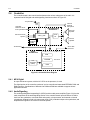
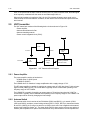
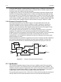
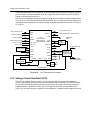
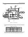
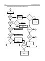
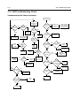
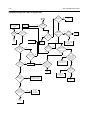
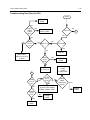
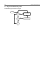
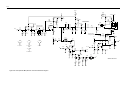
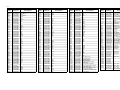
1
PRO3150 ™ PRO3150 ™ Portable Radio contact contact PRO3150 control control C A , Motorola, Professional Radio, PRO Series, PRO3150, are trademaks of Motorola. LTR is a registered tademark of E.F. Johnson, Inc. SmarTrunk is a registered trademark of SmarTrunk Systems, Inc. Transcrypt is a registered tademark of Transcrypt International. © 1999 Motorola, Inc. All rights reserved. Printed in USA. *6881093C23-O* 68P81093C23-O Detailed Service Manual Professional Radio Portable Radio Computer Software Copyrights The Motorola products described in this manual may include copyrighted Motorola computer programs stored in semiconductor memories or other media. Laws in the United States and other countries preserve for Motorola certain exclusive rights for copyrighted computer programs, including the exclusive right to copy or reproduce in any form, the copyrighted computer program. Accordingly, any copyrighted Motorola computer programs contained in the Motorola products described in this manual may not be copied or reproduced in any manner without the express written permission of Motorola. Furthermore, the purchase of Motorola products shall not be deemed to grant, either directly or by implication, estoppel or otherwise, any license under the copyrights, patents or patent applications of Motorola, except for the normal non-exclusive royalty-free license to use that arises by operation of law in the sale of a product. 1999 by Motorola, Inc. 8000 W. Sunrise Blvd., Ft. Lauderdale, Fl 33322, U.S.A. All rights reserved. Printed in U.S.A. iii Safety Information Important information on safe and efficient operation is included in this manual. Read this information before using your radio. SAFE AND EFFICIENT OPERATION OF MOTOROLA TWO-WAY RADIOS This document provides information and instructions for the safe and efficient operation of Motorola Portable and Mobile Two-Way Radios. The information provided in this document supersedes the general safety information contained in user guides published prior to January 1, 1998. For information regarding radio use in hazardous areas, please refer to the Factory Mutual (FM) approval manual supplement or Instruction Card which is included with radio models that offer this capability EXPOSURE TO RADIO FREQUENCY ENERGY Your Motorola Two-Way Radio, which generates and radiates radio frequency (RF) electromagnetic energy (EME), is designed to comply with the following National and International Standards and Guidelines regarding exposure of human beings to radio frequency electromagnetic energy: ● Federal Communications Commission Report and Order No. FCC 96-326 (August 1996) ● American National Standards Institute (C95.1 - 1992) ● National Council on Radiation Protection and Measurements (NCRP-1986) ● International Commission on Non-Ionizing Radiation Protection (ICNRP- 1986) ● European Committee for Electrotechnical Standardization (CENELEC): - ENV 50166-1 1995 E Human exposure to electromagnetic fields Low frequency (0 Hz to 10 kHz) - ENV 50166-2 1995 E Human exposure to electromagnetic fields High frequency (10 kHz to 300 GHz) - Proceedings of SC211/B 1996 “Safety Considerations for Human Exposure to EMFs from Mobile Telecommunication Equipment (MTE) in the Frequency Range 30MHz - 6 GHz.” (EMF - Electromagnetic Fields) To assure optimal radio performance and to ensure that your exposure to radio frequency electromagnetic energy is within the guidelines in the above standards, always adhere to the following procedures: PORTABLE RADIO OPERATION AND EME EXPOSURE ● When transmitting with a portable radio, hold radio in a vertical position with the microphone 2.5 to 5.0 centimeters (one to two inches) away from the mouth. Keep antenna at least 2.5 centimeters (one inch) from your head or body when transmitting. ● If you wear a portable Two-Way radio on your body, ensure that the antenna is at least 2.5 centimeters (one inch) from the body when transmitting. 2.5 to 5.0 cm (1 to 2 in.) iv ELECTROMAGNETIC INTERFERENCE/COMPATIBILITY NOTE Nearly every electronic device is susceptible to electromagnetic interference (EMI) if inadequately shielded, designed, or alternately configured for electromagnetic compatibility. ● To avoid electromagnetic interference and/or compatibility conflicts, turn off your radio in any facility where posted notices instruct you to do so. Hospital or health facilities may be using equipment that is sensitive to external RF energy. ● When instructed to do so, turn off your radio when on board an aircraft. Any use of a radio must be in accordance with airline regulations or crew instructions. OPERATIONAL WARNINGS Vehicles with an Air Bag ! WARNING: Do not place a portable radio in the area over an air bag or in the air bag deployment area. Air bags inflate with great force. If a portable radio is placed in the air bag deployment area and the air bag inflates, the radio may be propelled with great force and cause serious injury to occupants of vehicle. Potentially Explosive Atmospheres ! WARNING: Turn off your Two-Way radio when you are in any area with a potentially explosive atmosphere, unless it is a radio type especially qualified for use in such areas (e.g. FM or Cenelec approved). Sparks in a potentially explosive atmosphere can cause an explosion or fire resulting in bodily injury or even death. Batteries ! WARNING: Do not replace or recharge batteries in a potentially explosive atmosphere. Contact sparking may occur while installing or removing batteries and cause an explosion. Blasting Caps and Areas ! NOTE WARNING: To avoid possible interference with blasting operations, turn off your radio when you are near electrical blasting caps. In a “blasting area” or in areas posted “turn off two-way radio”, obey all signs and instructions. The areas with potentially explosive atmospheres referred to above include fuelling areas such as: below decks on boats; fuel or chemical transfer or storage facilities; areas where the air contains chemicals or particles, such as grain, dust or metal powders; and any other area where you would normally be advised to turn off your vehicle engine. Areas with potentially explosive atmospheres are often but not always posted. OPERATIONAL CAUTIONS Damaged Antennas ! CAUTION: Do not use any portable two-way radio that has a damaged antenna. If a damaged antenna comes into contact with your skin, a minor burn can result. Batteries ! CAUTION: All batteries can cause property damage and/or bodily injury such as burns if a conductive material such as jewelry, keys or beaded chains touch exposed terminals. The conductive material may complete an electrical circuit (short circuit) and become quite hot. Exercise care in handling any charged battery, particularly when placing it inside a pocket, purse or other container with metal objects. -1 Chapter 1 Introduction 1.1 Scope of Manual This manual is intended for use by service technicians familiar with similar types of equipment. It contains service information required for the equipment described and is current as of the printing date. Changes which occur after the printing date are incorporated by a complete Manual revision or alternatively, as additions. NOTE Before operating or testing these units, please read the Safety Information section in the front of this manual. 1.2 Warranty and Service Support Motorola offers long term support for its products. This support includes full exchange and/or repair of the product during the warranty period, and service/ repair or spare parts support out of warranty. Any “return for exchange” or “return for repair” by an authorized Motorola Dealer must be accompanied by a Warranty claim form. Warranty claim forms are obtained by contacting customer service. 1.2.1 Warranty Period The terms and conditions of warranty are defined fully in the Motorola Dealer or Distributor or Reseller contract. These conditions may change from time to time and the following notes are for guidance purposes only. 1.2.2 Return Instructions In instances where the product is covered under a “return for replacement” or “return for repair” warranty, a check of the product should be performed prior to shipping the unit back to Motorola. This is to ensure that the product has been correctly programmed or has not been subjected to damage outside the terms of the warranty. 1.2.3 After Warranty Period After the Warranty period, Motorola continues to support its products in two ways. Firstly, Motorola's Accessories and Aftermarket Division (AAD) offers a repair service to both end users and dealers at competitive prices. Secondly, Motorola’s service department supplies individual parts and modules that can be purchased by dealers who are technically capable of performing fault analysis and repair. 1.3 Related Documents The following documents are directly related to the use and maintainability of this product. Title Part Number Service Manual, Basic, Spanish Service Manual, Basic, Portuguese Service Manual, Basic, English Service Manual, Detailed, Spanish Service Manual, Detailed, Portuguese 68P81093C27 68P81093C28 68P81093C22 68P81093C29 68P81093C30 -2 1.4 Technical Support Technical Support Technical support is available to assist the dealer/distributor and self-maintained customers in resolving any malfunction which may be encountered. Initial contact should be by telephone to customer resources wherever possible. When contacting Motorola technical support, be prepared to provide the product model number and the unit’s serial number. The contact locations and telephone numbers are located in the Basic Service Manual listed under the Related Documents paragraph of this section. 1.4.1 Piece Parts Some replacement parts, spare parts, and/or product information can be ordered directly. If a complete Motorola part number is assigned to the part, it is available from Motorola’s Accessories and Aftermarket Division (AAD). If no part number is assigned, the part is not normally available from Motorola. If the part number is appended with an asterisk, the part is serviceable by Motorola Depot only. If a parts list is not included, this generally means that no user-serviceable parts are available for that kit or assembly. All orders for parts/information should include the complete Motorola identification number. All part orders should be directed to your local AAD office. Please refer to your latest price pages. Parts Order Entry 7:00 A. M. to 7:00 P. M. (Central Standard Time) Monday through Friday (Chicago, U. S. A.) To Order Parts in Latin America and the Caribbean: (847) 538-8023 Motorola Parts Accessories and Aftermarket Division Latin America and Caribbean Attention: Order Processing 1313 E. Algonquin Road Schaumburg, IL 60196 1.5 Order Processing 1313 E. Algonquin Road Schaumburg, IL 60196 Parts Identification (847) 538-0021 (Voice) 847) 538-8194 (FAX) Radio Model Chart and Specifications The radio model charts and specifications are located in the Basic Service Manual listed under the Related Documents paragraph of this chapter. 1.6 Radio Model Information The model number and serial number are located on a label attached to the back of your radio. You can determine the RF output power, frequency band, protocols, and physical packages from these numbers. The example below shows one portable radio model number and its specific characteristics. Radio Model Information -3 Table 1-1 Radio Model Number (Example: LAH34KDC9AA1AN) Model Series Freq. Band Power Level H 34 K VHF (136-174 MHz) D 4-5W Physical Channel Packages Spacing Protocol Feature Model Model Level Revision Package C 9 AA No Prog- Conventional Display rammable 1 4F H 1-Line Display 6 16F H = Portable LA = Motorola Internal Use LA Type of Unit R UHF R1 (403-470 MHz) S UHF R2 (450527) A N -4 Radio Model Information Notes __________________________________________________________________________ __________________________________________________________________________ __________________________________________________________________________ __________________________________________________________________________ __________________________________________________________________________ __________________________________________________________________________ __________________________________________________________________________ __________________________________________________________________________ __________________________________________________________________________ __________________________________________________________________________ __________________________________________________________________________ __________________________________________________________________________ __________________________________________________________________________ __________________________________________________________________________ __________________________________________________________________________ __________________________________________________________________________ __________________________________________________________________________ __________________________________________________________________________ __________________________________________________________________________ __________________________________________________________________________ __________________________________________________________________________ __________________________________________________________________________ __________________________________________________________________________ __________________________________________________________________________ __________________________________________________________________________ __________________________________________________________________________ __________________________________________________________________________ __________________________________________________________________________ __________________________________________________________________________ __________________________________________________________________________ __________________________________________________________________________ __________________________________________________________________________ __________________________________________________________________________ __________________________________________________________________________ __________________________________________________________________________ i TABLE OF CONTENTS Safe And Efficient Operation Of Motorola Two-way Radios .............................iii Exposure To Radio Frequency Energy.............................................................iii Portable Radio Operation And EME Exposure .................................................iii Electromagnetic Interference/Compatibility ......................................................iv Operational Warnings .......................................................................................iv Operational Cautions ........................................................................................iv Introduction 1.1 Scope of Manual.................................................................................................. 1-1 1.2 Warranty and Service Support............................................................................. 1-1 1.2.1 Warranty Period ............................................................................................. 1-1 1.2.2 Return Instructions......................................................................................... 1-1 1.2.3 After Warranty Period .................................................................................... 1-1 1.3 Related Documents ............................................................................................. 1-1 1.4 Technical Support................................................................................................ 1-2 1.4.1 Piece Parts..................................................................................................... 1-2 1.5 Radio Model Chart and Specifications................................................................. 1-2 1.6 Radio Model Information...................................................................................... 1-2 Theory of Operation 2.1 Introduction .......................................................................................................... 2-1 2.2 Radio Power Distribution ..................................................................................... 2-1 2.3 Keypad................................................................................................................. 2-3 2.4 Controller ............................................................................................................. 2-4 2.4.1 MCU Digital.................................................................................................... 2-4 2.4.2 Audio/Signaling .............................................................................................. 2-4 2.5 UHF Transmitter .................................................................................................. 2-5 2.5.1 Power Amplifier (PA)...................................................................................... 2-5 2.5.2 Antenna Switch .............................................................................................. 2-5 2.5.3 Harmonic Filter............................................................................................... 2-6 2.5.4 Antenna Matching Network............................................................................ 2-6 2.5.5 Power Control Integrated Circuit (PCIC)........................................................ 2-6 2.5.6 Temperature Cut Back Circuit........................................................................ 2-6 2.6 UHF Receiver ...................................................................................................... 2-7 2.6.1 Receiver Front-End........................................................................................ 2-7 2.6.2 Receiver Back-End ........................................................................................ 2-8 2.6.3 Automatic Gain Control (AGC)....................................................................... 2-8 2.6.4 Frequency Generation Circuit ........................................................................ 2-9 2.7 Synthesizer .......................................................................................................... 2-9 2.8 Voltage Control Oscillator (VCO)....................................................................... 2-10 2.9 VHF Transmitter ................................................................................................ 2-12 ii 2.9.1 Power Amplifier ............................................................................................2-12 2.9.2 Antenna Switch ............................................................................................2-12 2.9.3 Harmonic Filter .............................................................................................2-13 2.9.4 Antenna Matching Network ..........................................................................2-13 2.9.5 Power Control Integrated Circuit (PCIC) ......................................................2-13 2.10 VHF Receiver.....................................................................................................2-14 2.10.1 Receiver Front-End ......................................................................................2-14 2.10.2 Receiver Back-End.......................................................................................2-15 2.10.3 Automatic Gain Control (AGC) .....................................................................2-15 2.10.4 Frequency Generation Circuitry....................................................................2-16 2.11 Synthesizer ........................................................................................................2-16 2.12 Voltage Control Oscillator (VCO) .......................................................................2-17 Maintenance 3.1 Introduction ..........................................................................................................3-1 3.2 Preventive Maintenance.......................................................................................3-1 3.2.1 Inspection .......................................................................................................3-1 3.2.2 Cleaning .........................................................................................................3-1 3.3 Safe Handling of CMOS and LDMOS ..................................................................3-2 3.4 General Repair Procedures and Techniques.......................................................3-2 3.5 Recommended Test Tools ...................................................................................3-4 3.6 Replacing the Circuit Board Fuse ........................................................................3-5 3.7 Removing and Reinstalling the Circuit Board.......................................................3-6 3.8 Power Up Self-Test Error Codes..........................................................................3-7 3.9 UHF Troubleshooting Charts ...............................................................................3-8 3.10 VHF Troubleshooting Charts..............................................................................3-14 3.11 Keypad Troubleshooting Chart ..........................................................................3-20 Schematic Diagrams, Overlays, and Parts Lists 4.1 Introduction ..........................................................................................................4-1 4.1.1 Notes For All Schematics and Circuit Boards.................................................4-1 4.1.2 Six Layer Circuit Board...................................................................................4-2 4.2 Flex Layout...........................................................................................................4-2 4.3 Keypad-Controller Interconnect Flex Schematic..................................................4-3 4.3.1 Keypad Top and Bottom Overlays .................................................................4-4 4.4 Speaker Microphone Schematic ..........................................................................4-5 4.4.1 Speaker Microphone Assembly......................................................................4-5 Introduction 2-1 Chapter 2 Theory of Operation 2.1 Introduction This chapter provides a detailed theory of operation for the radio components. Schematic diagrams for the circuits described in the following paragraphs are located in Chapter 4 of this manual. 2.2 Radio Power Distribution A block diagram of the DC power distribution throughout the radio board is shown in Figure 2-1. A 7.5V battery supplies the basic radio power (UNSWB) directly to the electronic on/off control, audio power amplifier, power amplifier automatic level control (ALC), and low battery detect circuit. When the radio on/off/volume control is turned on, the switched SWB+ is applied to the various radio power regulators, antenna switch, accessories jack, and keypad/option board, and transmit LED. The Vdda output from the 3.3V Vdda regulator supplies the microprocessor with operating power. Data is then sent to the controller ASFIC to turn on a DAC which takes over the momentary-on path within 12ms. The SWB+ signal supplies power until the radio is turned off. Jumpers for configuring the Vdda and Vddd regulators are shown in Figure 2-1 and described in Table 2-1. The radio turns off when either of the following two conditions occur: • Radio on/off/volume control is turned off. • Low battery condition is detected. If a low battery level is detected by the microprocessor through either of the above conditions, the radio personality data is stored to EEPROM prior to turning off. 2-2 Radio Power Distribution Accessory Jacks Keypad/Option Board Audio PA UNSWB+ R4 7.5V Fuse Battery SWB+ Vdda Vdda Reg. R2 R3 R1 Vddd Reg. Vdda Tx Led MCU Micro P, ROM & EEPROM Control MECH. SWB+ On/Off Switch FRACTN LCD Driver ASFIC_CMPVCOBIC LVZIF 5V Reg. Low Battery Detect 5V Ant. SW PA, Driver PCIC(ALC) RF. AMP, IF AMP Ext. Rx Buffer (NU) Figure 2-1. DC Power Distribution Block Diagram Table 2-1 Radio Jumpers Jumpers Dual Vdd Regulator Scheme Single Vdd Regulator Scheme R1 R2 R3 R4 Y N N Y Y N Y N Keypad Keypad The keypad block diagram is shown in Figure 2-2. The comparator compares the voltage when any one of the keypad row or keypad column keys is pressed. Pressing a key sends a message to the microprocessor through the output (KEY_INT) line signifying that a key has been pressed. The microprocessor then samples the Analog to Digital voltages at the keypad row and keypad column, and makes a comparison with a map table to identify the key pressed. Keypad Column Data 9 pin connector 2.3 2-3 40 pin connector Keypad Row Key_Int Comparator Figure 2-2. Keypad Block Diagram Keypad Button 2-4 2.4 Controller Controller The controller board is the central interface between the various subsystems of the radio. It is separated into MCU digital and audio/signalling functions as shown in Figure 2-3. To Synthesizer Mod Out Internal/ External Microphone 16.8 MHz Reference Clock from Synthesizer Audio/Signalling Architecture Recovered Audio Squelch Audio PA ASFIC_CMP Internal Speaker 3.3V Regulator (Vdda) µP Clock SPI To RF Board External Speaker SCI to Side Connector Digital Architecture RAM 3.3V Regulator (Vddd) EEPROM HC11FL0 ROM Figure 2-3. Controller Block Diagram 2.4.1 MCU Digital An open architecture system, with the HC11FL0 as the processor, is used. The digital portion of the controller consists of a micro controller and associated EEPROM, RAM, and ROM memories. Combinations of different size RAM and ROM are available to support various application software. 2.4.2 Audio/Signaling The audio/signalling/filter/companding IC (ASFIC) and the audio power amplifier (Figure 2-3) form the main components of the audio/signalling section of the controller board. Inputs include a 16.8 MHz clock from the synthesizer, recovered audio and squelch, microprocessor, and external or internal microphones. Outputs include a microprocessor clock (CLK), modulator output to the synthesizer, and amplified audio signals to an internal or external speaker. UHF Transmitter 2.5 2-5 UHF Transmitter The UHF transmitter consists of the following basic circuits as shown in Figure 2-4. • • • • Power amplifier (PA) Antenna switch/harmonic filter Antenna matching network Power control integrated circuit (PCIC) PCIC From VCO Antenna Jack Vcontrol Vcontrol PA Driver PA-Final Stage Antenna Switch/ Matching Network/ Harmonic Filter Figure 2-4. UHF Transmitter Block Diagram 2.5.1 Power Amplifier (PA) The PA consists of two LDMOS devices: 1. PA driver, U101 2. PA final stage, Q110 The LDMOS driver (U101) provides 2-stage amplification using a supply voltage of 7.3V. The amplifier is capable of supplying an output power of 0.3W (U101-6 and -7) with an input signal of 2mW at 3dBm at U101-16. The current drain is typically 160mA while operating in the frequency range of 403470MHz (Band 1) or 450-527 MHz (Band 2). The LDMOS PA is capable of supplying an output power of 7W with an input signal of 0.3W. The current drain is typically 1300mA while operating in the frequency range of 403-470MHz. The power output can be varied by changing the bias voltage. 2.5.2 Antenna Switch The antenna switch circuit consists of two PIN diodes (CR101 and CR102), a pi network (C107, L104 and C106) and two current limiting resistors (R101 and R170). In the transmit mode, B+ at PCIC (U102) pin 23 goes low turning on Q111 which applies a B+ bias to the antenna switch circuit to bias the diodes “on”. The shunt diode (CR102) shorts out the receiver port and the pi network. This operates as a quarter wave transmission line to transform the low impedance of the shunt diode to a high impedance at the input of the harmonic filter. In the receive mode, the diodes are both off, creating a low attenuation path between the antenna and receiver ports. 2-6 UHF Transmitter 2.5.3 Harmonic Filter The harmonic filter consists of C104, L102, C143, C103, L101, C142 and C102. The harmonic filter for UHF is a modified Zolotarev design optimized for efficiency of the power module. This type of filter has the advantage that it can give a greater attenuation in the stop-band for a given ripple level. The harmonic filter insertion loss is typically less than 1.2dB. 2.5.4 Antenna Matching Network The matching network (L116 and C141) matches the antenna's impedance with the harmonic filter to optimize the performance of the transmitter and receiver. 2.5.5 Power Control Integrated Circuit (PCIC) The transmitter uses the PCIC (U102) to regulate the power output of the radio. The current to the final stage of the power module is supplied through R102, which provides a voltage proportional to the current drain. This voltage is then fed back to the Automatic Level Control (ALC) within the PCIC to regulate the output power of the transmitter. The PCIC contains internal digital to analog converters (DACs) that provide a programmable control loop reference voltage. The reference voltage level is programmable through the SPI line of the PCIC. The PCIC internal resistors, integrators, and external capacitors (C133, C134 and C135) control the transmitter rise and fall times to reduce the power splatter into adjacent channels. 2.5.6 Temperature Cut Back Circuit Diode CR105 and associated components are part of a temperature cut back circuit. This circuit senses the printed circuit board temperature around the transmitter circuits and outputs a DC voltage to the PCIC. If the DC voltage produced exceeds the set threshold in the PCIC, the transmitter output power decreases to reduce the transmitter temperature. UHF Receiver 2.6 2-7 UHF Receiver The UHF receiver consists of front end, back end, and automatic gain control circuits. A block diagram of the receiver is shown in Figure 2-5. Detailed descriptions of these stages are contained in the paragraphs that follow. Antenna RF Jack Pin Diode Antenna Switch Varactor Tuned Filter RF Amp Varactor Tuned Filter Mixer Crystal Filter IF Amp AGC Control Voltage from ASFIC First LO from FGU Recovered Audio Squelch Demodulator U301 RSSI IF IC Synthesizer 16.8 MHz Reference Clock SPI Bus Second LO VCO Figure 2-5. UHF Receiver Block Diagram 2.6.1 Receiver Front-End The RF signal received by the antenna is applied to a low-pass filter. For UHF, the filter consists of components L101, L102, C102, C103, and C104. The filtered RF signal is passed through the antenna switch circuit consisting of two PIN diodes (CR101 and CR102) and a pi network (C106, L104, and C107). The signal is then applied to a varactor tuned filter bandpass. The UHF bandpass filter consists of components L301, L302, C302, C303, C304, CR301, and CR302. The filter is electronically tuned by DACRx from IC 404 which supplies a control voltage to the varactor diodes (CR301 and CR302) in the filter, as determined by the microprocessor, depending on the carrier frequency. Wideband operation of the filter is achieved by shifting the bandpass filter across the band. The output of the bandpass filter is coupled to the RF amplifier transistor Q301 via C307. After being amplified by the RF amplifier, the RF signal is further filtered by a second varactor tuned bandpass filter, consisting of L306, L307, C313, C317, CR304 and CR305. Both the pre and post-RF amplifier varactor tuned filters have similar responses. The 3 dB bandwidth of the filter is approximately 50 MHz. This enables the filters to be electronically controlled by using a single control voltage from DACRx. 2-8 UHF Receiver The output of the post-RF amplifier filter is connected to the passive double balanced mixer consisting of components T301, T302, and CR306. Matching of the filter to the mixer is provided by C381. After mixing with the first local oscillator (LO) signal from the voltage controlled oscillator (VCO) using low side injection, the RF signal is down-converted to a 45.1 MHz IF signal. The IF signal coming out of the mixer is transferred to the crystal filter (FL301) through a resistor pad and a diplexer (C322 and L310). Matching to the input of the crystal filter is provided by C324 and L311. The crystal filter provides the necessary selectivity and intermodulation protection. 2.6.2 Receiver Back-End The output of crystal filter FL301 is matched to the input of IF amplifier transistor Q302 by components R352 and C325. Voltage supply to the IF amplifier is taken from the receive 5 volts (R5). The IF amplifer provides a gain of about 7dB. The amplified IF signal is then coupled into U301, pin 3 via C330, C338 and L330 which provides the matching for the IF amplifier and U301. The IF signal applied to pin 3 of U301 is amplified, down-converted, filtered, and demodulated, to produce the recovered audio at U301, pin 27. This IF IC (U301) is electronically programmable, and the amount of filtering (which is dependent on the radio channel spacing) is controlled by the microprocessor. Additional filtering, once externally provided by the conventional ceramic filters, is replaced by internal filters in the IF IC. The IF IC uses a type of direct conversion process, whereby the externally generated second LO frequency is divided by two in U301 so that it is very close to the first IF frequency. The IF IC synthesizes the second LO and phase-locks the VCO to track the first IF frequency. The second LO is designed to oscillate at twice the first IF frequency because of the divide-by-two function in the IF IC. In the absence of an IF signal, the VCO searches for a frequency, or its frequency will vary close to twice the IF frequency. When an IF signal is received, the VCO locks onto the IF signal. The second LO/VCO is a Colpitts oscillator built around transistor Q320. The VCO has a varactor diode, CR310, to adjust the VCO frequency. The control signal for the varactor is derived from a loop filter consisting of C362, C363, C364, R320 and R321. The IF IC also performs several other functions. It provides a received signal-strength indicator (RSSI) and a squelch output. The RSSI is a dc voltage monitored by the microprocessor, and used as a peak indicator during the bench tuning of the receiver front-end varactor filter. The RSSI voltage is also used to control the automatic gain control (AGC) circuit at the front-end. The demodulated signal on pin 27 of U301 is also used for squelch control. The signal is routed to U404 (ASFIC) where squelch signal shaping and detection takes place. The demodulated audio signal is also routed to U404 for processing before going to the audio amplifier for amplification. 2.6.3 Automatic Gain Control (AGC) The front end automatic gain control circuit provides automatic reduction of gain for the front end RF amplifier via feedback. This prevents overloading of backend circuits by drawing some of the output power from the RF amplifier output. At high radio frequencies, capacitor C331 provides a low impedance path to ground for this purpose. CR308 is a PIN diode used for switching the path on or off. A certain amount of forward biasing current is needed to turn the PIN diode on. Transistor Q315 provides this current where, upon saturation, current will flow via R347, PIN diode, collector and emitter of Q315 and R319 before going to ground. Q315 is an NPN transistor used for switching. Maximum current flowing through the pin is limited mainly by the resistor R319. The radio signal strength indicator (RSSI) voltage signal is used to drive Q315 to saturation, i.e., turned on. RSSI is produced by U301 and is proportional to the gain of the RF amplifier and the input power to the radio. The resistor network at the input to the base of Q315 is scaled to turn on Q315, activating the AGC, at certain RSSI levels. To turn on Q315, the voltage across the transistor’s base to ground must be greater or equal to the voltage across R319, plus the base-emitter voltage (Vbe) present at Q315. The resistor network with thermistor RT300 is capable of providing temperature compensation to the AGC Synthesizer 2-9 circuit, as RSSI generated by U301 is lower at cold temperatures compared to normal operation at room temperature. Resistor R300 and capacitor C397 form an R-C network used to dampen any transient instability while the AGC is turning on. 2.6.4 Frequency Generation Circuit The frequency generation circuit, shown in Figure2-6, is composed of Fractional-N synthesizer U201 and VCO/Buffer IC U241. Designed in conjunction to maximize compatibility, the two ICs provide many of the functions that normally require additional circuitry. The synthesizer block diagram illustrates the interconnect and support circuitry used in the region. Refer to the schematic to locate reference designators. The synthesizer is powered by regulated 5V and 3.3V, which are provided by ICs U247 and U248 respectively. The 5V signal goes to U201-13 and -30 while the 3.3V signal goes to U201-5, -20, -34 and -36. The synthesizer in turn generates a superfiltered 4.5V signal to power U241. In addition to the VCO, the synthesizer also interfaces with the logic and ASFIC circuits. Programming for the synthesizer is accomplished through the data, clock and chip select lines from the microprocessor. A 3.3V dc signal from the synthesizer lock detect line indicates to the microprocessor that the synthesizer is locked. Transmit modulation from the ASFIC is supplied to U201, pin 10. Internally, the audio is digitized by the Fractional-N and applied to the loop divider to provide the low-port modulation. The audio runs through an internal attenuator for modulation balancing purposes before going to the VCO. Dual Transistor Voltage Multiplier TRB VCP Aux3 Vmult1 Vmult2 Synthesizer U201 16.8 MHz Ref. Osc. Rx VCO Circuit Aux4 Loop Filter MOD Out Rx Out Matching Network Low Pass Filter Attenuator To PA Driver To Mixer VCOBIC U241 Tx Out Tx VCO Circuit Modulating Signal Figure 2-6. 2.7 Frequency Generation Unit Block Diagram Synthesizer The Fractional-N Synthesizer, shown in Figure 2-7, uses a 16.8MHz crystal (FL201) to provide a reference for the system. The LVFractN IC (U201) further divides this to 2.1MHz, 2.225MHz, and 2.4MHz as reference frequencies. Together with C206, C207, C208, R204 and CR203, they build up the reference oscillator which is capable of 2.5ppm stability over temperatures of -30 to 85°C. It also provides 16.8MHz at pin 19 of U201 to be used by ASFIC and LVZIF. The loop filter consists of C231, C232, C233, R231, R232 and R233. This filter provides the necessary dc steering voltage for the VCO and determines the amount of noise and spur passing through. 2-10 Voltage Controlled Oscillator (VCO) To achieve fast locking for the synthesizer, an internal adapt charge pump provides higher current at pin 45 of U201 to put the synthesizer within the lock range. The required frequency is then locked by normal mode charge pump at U201, pin 43. Both the normal and adapt charge pumps get their supply from the capacitive voltage multiplier made up of C258, C259, C228, triple diode CR201 and level shifters U210 and U211. Two 3.3V square waves, 180 degrees out of phase, are first shifted to 5V, then along with regulated 5V, put through arrays of diodes and capacitors to build up 13.3V at U201-47. 7 DATA (U409 PIN 100) 8 CLOCK (U409 PIN 1) 9 CSX (U409 PIN 2) 10 MOD IN (U404 PIN 40) 13, 30 +5V (U247 PIN 4) (U248 PIN 5) LOCK 4 LOCK (U409 PIN 56) 19 FREF (U201 PIN 21 & U404 PIN 34) DATA 5, 20, 34, 36 23 REFERENCE OSCILLATOR 24 25 32 47 VOLTAGE MULTIPLIER FREFOUT CLK GND U201 LOW VOLTAGE MODIN FRACTIONAL-N IOUT SYNTHESIZER IADAPT VCC, DC5V 6, 22, 23, 24 CEX MODOUT VDD, 3.3V 43 45 AUX4 3 XTAL2 AUX3 2 SFOUT 2-POLE LOOP FILTER 41 XTAL1 WARP STEERING LINE LO RF INJECTION DUAL TRANSIS TORS 28 FILTERED 5V PREIN BIAS1 VCP VMULT2 14 VOLTAGE CONTROLLED OSCILLATOR 40 VMULT1 AUX1 BIAS2 TxRF INJECTION (1ST STAGE OF PA) 39 15 48 DUAL 5V TRANSISTORS R5 PRESCALER IN Figure 2-7. 2.8 UHF Synthesizer Block Diagram Voltage Controlled Oscillator (VCO) The VCOB IC (U241), shown in Figure 2-8, in conjunction with the Fractional-N synthesizer (U201) generates RF in both the receive and the transmit modes of operation. The TRB line (U241-19) determines which oscillator and buffer are enabled. A sample of the RF signal from the enabled oscillator is routed from U241-12, through a low pass filter, to the prescaler input (U201-32). After frequency comparison in the synthesizer, a resultant DC control voltage is received at the VCO. When the PLL is locked on frequency, this voltage can vary between 3.5 V and 9.5V. The VCOB IC (U241) is operated at 4.54 V (VSF) and Fractional-N synthesizer (U201) at 3.3V. This difference in operating voltage requires a level shifter consisting of Q260 and Q261 on the TRB line. Voltage Controlled Oscillator (VCO) 2-11 The operation logic is shown in Table 2-2. 5V AUX3 (U201 Pin2) Level Shifter Network AUX4 (U201 Pin3) U201 Pin 32 Prescaler Out TRB_IN Pin 20 Rx-SW Pin7 Tx-SW Pin13 Pin 19 Pin 12 Tx/Rx/BS Switching Network LO RF INJECTION Presc Vcc-Superfilter (U201 Pin28) VSF Steer Line Voltage (VCTRL) Matching Network U241 VCOBIC Pin3 Low Pass Filter Collector/RF in Pin4 Rx Rx Rx Tank Rx VCO Circuit Rx Active Bias Pin5 Pin8 VSF (U201 Pin28) Pin14 Pin6 Tx Tx Tank Tx VCO Circuit Tx Active Bias Pin16 Tx VCC Buffers Pin10 Tx RF Injection Attenuator Pin15 Vsens Circuit Pin18 Vcc-Logic Pin2 Pin1 Rx-I adjust Tx-I adjust Pins 9,11,17 VSF (U201 Pin28) Figure 2-8. VCO Block Diagram Table 2-2 Level Shifter Logic Desired Mode AUX 4 AUX 3 TRB Tx Low High (@3.2V) High (@4.8V) Rx High Low Low Battery Saver Low Low Hi-Z/Float (@2.5V) In the receive mode, U241-19 is low or grounded. This activates the receive VCO by enabling the receive oscillator and the receive buffer of U241. The RF signal at U241- 8 is run through a matching network. The resulting LO RF INJECTION RF signal is applied to the mixer at T302. When PTT is pressed during the transmit condition, five volts is applied to U241-19. This activates the transmit VCO by enabling the U241 transmit oscillator and buffer. The TX RF INJECTION signal at 2-12 VHF Transmitter U241-10 is injected into the input of the PA module (U101-16). Also in transmit mode, the audio signal to be frequency modulated onto the carrier is received through U201-41. When a high impedance is applied to U241-19, the VCO operates in battery saver mode. In this mode, both the receive and transmit oscillators, as well as the receive transmit and prescaler buffer, are turned off. 2.9 VHF Transmitter The VHF transmitter consists of the following basic circuits as shown in Figure 2-9: •Power amplifier. •Antenna switch/harmonic filter. •Antenna matching network. •Power control integrated circuit (PCIC). PCIC From VCO PA Driver Figure 2-9. Antenna Jack Vcontrol Vcontrol PA-Final Stage Antenna Switch/ Matching Network/ Harmonic Filter VHF Transmitter Block Diagram 2.9.1 Power Amplifier The power amplifier consists of two devices: •LDMOS driver IC (U3501) and •LDMOS PA (Q3501) The LDMOS driver IC contains a 2-stage amplification with a supply voltage of 7.3V. This RF power amplifier is capable of supplying an output power of 0.3W (pins 6 and 7) with an input signal of 2mW (3dBm) (pin16). The current drain is typically around 130mA while operating in the frequency range of 136-174MHz. The LDMOS PA is capable of supplying an output power of 7W with an input signal of 0.3W. The current drain is typically around 1800mA while operating in the frequency range of 136-174MHz. The power output can be varied by changing the bias voltage. 2.9.2 Antenna Switch The antenna switch circuit consists of two PIN diodes (D3521 and D3551), a pi network (C3531, L3551 and C3550), and three current limiting resistors (R3571, R3572, R3573). In the transmit mode, B+ at PCIC (U3502) pin 23 will go low and turn on Q3561 where a B+ bias is applied to the antenna switch circuit to bias the diodes “on”. The shunt diode (D3551) shorts out the receiver port and the pi network (which operates as a quarter wave transmission line), and transforms the low impedance of VHF Transmitter 2-13 the shunt diode to a high impedance at the input of the harmonic filter. In the receive mode, the diodes are both off, creating a low attenuation path between the antenna and receiver ports. 2.9.3 Harmonic Filter The harmonic filter consists of C3532 to C3536, L3531 and L3532. This network forms a low-pass filter to attenuate harmonic energy of the transmitter to specifications level. The harmonic filter insertion loss is typically less than 1.2dB. 2.9.4 Antenna Matching Network A matching network made up of L3538, C3537 and C3539 is used to match the antenna's impedance to the harmonic filter. This optimizes the performance of the transmitter and receiver into an antenna. 2.9.5 Power Control Integrated Circuit (PCIC) The transmitter uses the PCIC (U3502) to control the power output of the radio by maintaining the radio current drain. The current to the final stage of the power module is supplied through R3519, which provides a voltage proportional to the current drain. This voltage is then fed back to the Automatic Level Control (ALC) within the PCIC to provide loop stability. The PCIC also contains internal digital to analog converters (DACs) that provide the reference voltage of the control loop. The voltage level is controlled by the microprocessor through the data line of the PCIC. The resistors and integrators within the PCIC, and the external capacitors (C3562, C3563 and C3565) control the transmitter rise and fall time and are necessary to reduce the power splatter into adjacent channels. U3503 and its associated components act as a temperature cut back circuit. This provides the necessary voltage to the PCIC to cut the transmitter power if the radio temperature gets too high. 2-14 VHF Receiver 2.10 VHF Receiver The VHF receiver consists of front end, back end, and automatic gain control circuits. A block diagram of the VHF receiver is shown in Figure 2-10. Detailed descriptions of these features are contained in the paragraphs that follow. Antenna RF Jack Pin Diode Antenna Switch Varactor Tuned Filter RF Amp Varactor Tuned Filter Mixer Crystal Filter IF Amp AGC Control Voltage from ASFIC First LO from FGU Recovered Audio Squelch Demodulator U3220 RSSI IF IC Synthesizer 16.8 MHz Reference Clock SPI Bus Second LO VCO Figure 2-10. VHF Receiver Block Diagram 2.10.1 Receiver Front-End The RF signal is received by the antenna and applied to a low-pass filter consisting of L3531, L3532, C3532 to C3536. The filtered RF signal is passed through the antenna switch. The antenna switch circuit consists of two PIN diodes (D3521 and D3551) and a pi network (C3531, L3551 and C3550).The RF signal is then applied to a varactor tuned bandpass filter which consists of L3301, L3303, C3301 to C3304 and D3301. The filter is tuned by applying a control voltage to the varactor diode (D3301) in the filter. The bandpass filter is electronically tuned by the DACRx from IC U404 which is controlled by the microprocessor. Depending on the carrier frequency, the DACRx supplies the tuning voltage to the varactor diodes in the filter. Wideband operation of the filter is achieved by shifting the bandpass filter across the band. The output of the bandpass filter is coupled to the RF amplifier transistor Q3302 via C3306. After being amplified by the RF amplifier, the RF signal is further filtered by a second varactor tuned bandpass filter, consisting of L3305, L3306, C3311 to C3314 and D3302. Both the pre and post-RF amplifier varactor tuned filters have similar responses. The 3 dB bandwidth of the filter is about 12 MHz. This enables the filters to be electronically controlled by using a single control voltage which is DACRx. VHF Receiver 2-15 The output of the post-RF amplifier filter is connected to the passive double balanced mixer which consists of T3301, T3302 and CR3301. Matching of the filter to the mixer is provided by C3317, C3318 and L3308. After mixing with the first LO signal from the voltage controlled oscillator (VCO) using high side injection, the RF signal is down-converted to the 45.1 MHz IF signal. The IF signal coming out of the mixer is transferred to the crystal filter (Y3200) through a resistor pad (R3321 - R3323) and a diplexer (C3320 and L3309). Matching to the input of the crystal filter is provided by C3200 and L3200. The crystal filter provides the necessary selectivity and intermodulation protection. 2.10.2 Receiver Back-End The output of crystal filter Y3200 is matched to the input of IF amplifier transistor Q3200 by capacitor C3203. Voltage supply to the IF amplifier is taken from the receiver 5 volts (R5). The controlled gain IF amplifer provides a maximum gain of about 10dB. The amplified IF signal is then coupled into U3220 pin 3 via L3202, C3207, and C3230 which provides impedance matching for the IF amplifier and U3220. The IF signal applied to pin 3 of U3220 is amplified, down-converted, filtered, and then demodulated, to produce the recovered audio at pin 27 of U3220. This IF IC is electronically programmable, and the amount of filtering, which is dependent on the radio channel spacing, is controlled by the microprocessor. Additional filtering, once externally provided by the conventional ceramic filters, is replaced by internal filters in the IF module (U3220). The IF IC uses a type of direct conversion process, whereby the externally generated second LO frequency is divided by two in U3220 so that it is very close to the first IF frequency. The IF IC (U3220) synthesizes the second LO and phase-locks the VCO to track the first IF frequency. The second LO is designed to oscillate at twice the first IF frequency because of the divide-by-two function in the IF IC. In the absence of an IF signal, the VCO “searches” for a frequency, or its frequency will vary close to twice the IF frequency. When an IF signal is received, the VCO will lock onto the IF signal. The second LO/VCO is a Colpitts oscillator built around transistor Q3270. The VCO has a varactor diode, D3270, to adjust the VCO frequency. The control signal for the varactor is derived from a loop filter consisting of C3278 to C3280, R3274 and R3275. The IF IC (U3220) also provides a received signal-strength indicator (RSSI) and a squelch output. The RSSI is a dc voltage monitored by the microprocessor, and is used as a peak indicator during the bench tuning of the receiver front-end varactor filter. The RSSI voltage is also used to control the automatic gain control (AGC) circuit at the front-end. The demodulated signal on pin 27 of U3220 is also used for squelch control. The signal is routed to U404 (ASFIC) where squelch signal shaping and detection takes place. The demodulated audio signal is also routed to U404 for processing before going to the audio amplifier for amplification. 2.10.3 Automatic Gain Control (AGC) The front end automatic gain control circuit provides automatic reduction of gain of the front end RF amplifier via feedback. This prevents overloading of backend circuits and is achieved by drawing some of the output power from the RF amplifier output. At high radio frequencies, capacitor C3327 provides the low impedance path to ground for this purpose. CR3302 is a PIN diode used for switching the path on or off. A certain amount of forward biasing current is needed to turn the PIN diode on. Transistor Q3301 provides this current. Radio signal strength indicator, RSSI, a voltage signal, is used to drive Q3301 to saturation, i.e., turned on. RSSI is produced by U3220 and is proportional to the gain of the RF amplifier and the input power to the radio. Resistors R3304 and R3305 make up a voltage divider designed to turn on Q3301 at certain RSSI levels. To turn on Q3301 the voltage across R3305 must be greater or equal to the voltage across R3324, plus the base-emitter voltage (Vbe) present at Q3301. Capacitor C3209 is used to dampen any instability while the AGC is turning on. The current flowing into the collector of Q3301, a high 2-16 Synthesizer current gain NPN transistor, is drawn through the PIN diode to turn it on. Maximum current flowing through the pin is limited by resistors R3316, R3313, R3306 and R3324. Feedback capacitor C3326 is used to provide some stability to this high gain stage. An additional gain control circuit is formed by Q3201 and associated components. Resistors R3206 and R3207 are voltage dividers designed to turn on Q3201 at a significantly higher RSSI level than the level required to turn on PIN diode control transistor Q3301. In order to turn on Q3201 the voltage across R3207 must be greater or equal to the voltage across R3208 + Vbe. As current starts flowing into the collector of Q3201, it reduces the bias voltage at the base of IF amplifier transistor Q3200 and in turn, the gain of the IF amplifier. The gain is then controlled in a range of -30dB up to +10dB. 2.10.4 Frequency Generation Circuitry The Frequency Generation Circuitry shown in Figure 2-11is composed of two main ICs, the Fractional-N synthesizer (U3701), and the VCO/Buffer IC (U3801). Designed in conjunction to maximize compatibility, the two ICs provide many of the functions that normally would require additional circuitry. The synthesizer block diagram illustrates the interconnect and support circuitry used in the region. Refer to the schematic for the reference designators. The synthesizer is powered by regulated 5V and 3.3V which is provided from U3711 and U3201, respectively. The synthesizer, in turn, generates a superfiltered 4.5V which powers U3801. In addition to the VCO, the synthesizer must interface with the logic and ASFIC circuitry. Programming for the synthesizer is accomplished through the data, clock and chip select lines from the microprocessor. A 3.3V dc signal from synthesizer lock detect line indicates to the microprocessor that the synthesizer is locked. Transmit modulation from the ASFIC is supplied to pin10 of U3701. Internally, the audio is digitized by the Fractional-N and applied to the loop divider to provide low-port modulation. The audio runs through an internal attenuator for modulation balancing purposes before going out to the VCO. Voltage Multiplier TRB VCP Aux3 Vmult1 Vmult2 Synthesizer U3701 16.8 MHz Ref. Osc. MOD Out Rx VCO Circuit Loop Filter Rx Out To Mixer VCOBIC U3801 Tx Out To PA Driver Tx VCO Circuit Modulating Signal Figure 2-11. Frequency Generation Unit Block Diagram 2.11 Synthesizer The Fractional-N Synthesizer shown in Figure 2-12 uses a 16.8MHz crystal (Y3761) to provide a reference for the system. The LVFractN IC (U3701) further divides this to 2.1MHz, 2.225MHz, and 2.4MHz as reference frequencies. Together with C3761, C3762, C3763, R3761 and D3761, they build up the reference oscillator that is capable of 2.5 ppm stability over temperatures of -30 to 85°C. A 16.8MHz signal at pin 19 of U3701 is also provided for use by ASFIC and LVZIF. The loop filter which consists of C3721, C3722, R3721, R3722 and R3723 provides the necessary dc steering voltage for the VCO and determines the amount of noise and spur passing through. Voltage Control Oscillator (VCO) 2-17 In achieving fast locking for the synthesizer, an internal adapt charge pump provides higher current at pin 45 of U3701 to put the synthesizer within lock range. The required frequency is then locked by normal mode charge pump at pin 43. Both the normal and adapt charge pumps get their supply from the capacitive voltage multiplier made up of C3701 to C3704 and triple diodes D3701and D3702. Two 3.3V square waves (180 degrees out of phase) are first multiplied by four and then shifted, along with regulated 5V, to build up 13.5V at pin 47 of U3701. 7 DATA (U409 PIN 100) 8 CLOCK (U409 PIN 1) 9 CSX (U409 PIN 2) 10 MOD IN (U404 PIN 40) 13, 30 +5V (U3711 PIN 4) (U3201 PIN 5) LOCK 4 LOCK (U409 PIN 56) 19 FREF (U3220 PIN 21 & U404 PIN 34) DATA 5, 20, 34, 36 REFERENCE OSCILLATOR 23 24 25 32 47 VOLTAGE MULTIPLIER FREFOUT CLK GND U3701 LOW VOLTAGE MODIN FRACTIONAL-N IOUT SYNTHESIZER IADAPT VCC, DC5V 6, 22, 23, 24 CEX MODOUT VDD, 3.3V 43 45 AUX4 3 XTAL2 AUX3 2 SFOUT 2-POLE LOOP FILTER 41 XTAL1 WARP STEERING LINE LO RF INJECTION 28 FILTERED 5V PREIN BIAS1 VCP VMULT2 14 VOLTAGE CONTROLLED OSCILLATOR 40 VMULT1 AUX1 BIAS2 TxRF INJECTION (1ST STAGE OF PA) 39 15 48 DUAL 5V TSTRS R5 PRESCALER IN Figure 2-12. VHF Synthesizer Block Diagram 2.12 Voltage Control Oscillator (VCO) The VCOB IC (U3801), shown in Figure 2-13, in conjunction with the Fractional-N synthesizer (U3701), generates RF in both the receive and the transmit modes of operation. The TRB line (U3801, pin 19) determines which oscillator and buffer will be enabled. A sample of the RF signal from the enabled oscillator is routed from U3801, pin 12, through a low pass filter, to the prescaler input (U3701, pin 32). After frequency comparison in the synthesizer, a resultant control voltage is received 2-18 Voltage Control Oscillator (VCO) at the VCO. This voltage is a DC voltage typically between 3.5V and 9.5V when the PLL is locked on frequency. AUX3 (U3701 Pin2) U3701 Pin 32 Prescaler Out TRB_IN Pin 20 Rx-SW Pin7 Tx-SW Pin13 Pin 19 Pin 12 TX/RX/BS Switching Network LO RF INJECTION (U3701 Pin28) VSF Steer Line Voltage (VCTRL) Presc Vcc-Superfilter Matching Network U3801 VCOBIC Pin3 Low Pass Filter Collector/RF in Pin4 RX RX RX Tank RX VCO Circuit Rx Active Bias Pin5 Pin8 VSF (3701 Pin28) Pin14 Pin6 TX TX Tank TX VCO Circuit Tx Active Bias Pin16 TX VCC Buffers Pin10 TX RF Injection Attenuator Pin15 Vsens Circuit Pin18 Vcc-Logic Pin2 Pin1 Rx-I adjust Tx-I adjust Pins 9,11,17 VSF (U3701 Pin28) Figure 2-13. VCO Block Diagram The RF section of the VCOB IC(U3801) is operated at 4.54 V (VSF), while the control section of the VCOBIC and Fractional-N synthesizer (U3701) is operated at 3.3V. The operation logic is shown in Table 2-3. Table 2-3 VCO Control Logic Desired Mode AUX 4 AUX 3 TRB Tx Not Used High (@3.2V) High (@3.2V) Rx Not Used Low Low Battery Saver Not Used Hi-Z/Float (@1.6V) Hi-Z/Float (@1.6V) In the receive mode, U3801, pin 19 is low or grounded. This activates the receive VCO by enabling the receive oscillator and the receive buffer of U3801. The RF signal at U3801, pin 8 is run through a matching network. The resulting LO RF INJECTION signal is applied to the mixer at T3302. Voltage Control Oscillator (VCO) 2-19 During the transmit condition, when PTT is depressed, 3.2 volts is applied to U3801, pin 19. This activates the transmit VCO by enabling the transmit oscillator and the transmit buffer of U3801. The RF signal at U3801, pin 10 is injected into the input of the PA module (U3501, pin16). This RF signal is the TX RF INJECTION. Also in transmit mode, the audio signal to be frequency modulated onto the carrier is received through U3701, pin 41. When a high impedance is applied to U3801, pin19, the VCO is operating in battery saver mode. In this case, both the receive and transmit oscillators, as well as the receive transmit and prescaler buffer, are turned off. 2-20 Voltage Control Oscillator (VCO) Introduction 3-1 Chapter 3 Maintenance 3.1 Introduction This section of the manual describes: • preventive maintenance • safe handling of CMOS devices • repair procedures and techniques 3.2 Preventive Maintenance The radios do not require a scheduled preventive maintenance program; however, periodic visual inspection and cleaning is recommended. 3.2.1 Inspection Check that the external surfaces of the radio are clean, and that all external controls and switches are functional. It is not recommended to inspect the interior electronic circuitry. 3.2.2 Cleaning The following procedures describe the recommended cleaning agents and the methods to be used when cleaning the external and internal surfaces of the radio. External surfaces include the front cover, housing assembly, and battery case. These surfaces should be cleaned whenever a periodic visual inspection reveals the presence of smudges, grease, and/or grime. NOTE Internal surfaces should be cleaned only when the radio is disassembled for servicing or repair. The only recommended agent for cleaning the external radio surfaces is a 0.5% solution of a mild dishwashing detergent in water. The only factory recommended liquid for cleaning the printed circuit boards and their components is isopropyl alcohol (70% by volume). ! CAUTION: The effects of certain chemicals and their vapors can have harmful results on certain plastics. Aerosol sprays, tuner cleaners, and other chemicals should be avoided. 1. Cleaning External Plastic Surfaces The detergent-water solution should be applied sparingly with a stiff, non-metallic, short-bristled brush to work all loose dirt away from the radio. A soft, absorbent, lintless cloth or tissue should be used to remove the solution and dry the radio. Make sure that no water remains entrapped near the connectors, cracks, or crevices. 2. Cleaning Internal Circuit Boards and Components Isopropyl alcohol may be applied with a stiff, non-metallic, short-bristled brush to dislodge embedded or caked materials located in hard-to-reach areas. The brush stroke should direct the dislodged material out and away from the inside of the radio. Make sure that controls or tunable components are not soaked with alcohol. Do not use high-pressure air to hasten the drying process since this could cause the liquid to collect in unwanted places. Upon completion of the cleaning process, use a soft, absorbent, lintless cloth to dry the area. Do not brush or apply any isopropyl alcohol to the frame, front cover, or back cover. 3-2 Safe Handling of CMOS and LDMOS NOTE Always use a fresh supply of alcohol and a clean container to prevent contamination by dissolved material (from previous usage). 3.3 Safe Handling of CMOS and LDMOS Complementary metal-oxide semiconductor (CMOS) and lateral diffusion metal oxide semiconductor (LDMOS) devices are used in this family of radios. CMOS characteristics make them susceptible to damage by electrostatic or high voltage charges. Damage can be latent, resulting in failures occurring weeks or months later. Therefore, special precautions must be taken to prevent device damage during disassembly, troubleshooting, and repair. Handling precautions are mandatory for CMOS circuits and are especially important in low humidity conditions. DO NOT attempt to disassemble the radio without first referring to the CMOS CAUTION paragraph in the Disassembly and Reassembly section of the Basic Manual. 3.4 General Repair Procedures and Techniques 1. Parts Replacement and Substitution When damaged parts are replaced, identical parts should be used. If the identical replacement component is not locally available, check the parts list for the proper Motorola part number and order the component from the nearest Motorola Communications parts center listed in the “Piece Parts” section of this manual (See Chapter 1). 2. Rigid Circuit Boards This family of radios uses bonded, multi-layer, printed circuit boards. Since the inner layers are not accessible, some special considerations are required when soldering and unsoldering components. The printed-through holes may interconnect multiple layers of the printed circuit. Therefore, care should be exercised to avoid pulling the plated circuit out of the hole. When soldering near the 20-pin and 40-pin connectors: • avoid accidentally getting solder in the connector. • be careful not to form solder bridges between the connector pins • closely examine your work for shorts due to solder bridges. 3. Flexible Circuits The flexible circuits are made from a different material than the rigid boards and different techniques must be used when soldering. Excessive prolonged heat on the flexible circuit can damage the material. Avoid excessive heat and excessive bending. For parts replacement, use the ST-1087 Temperature-Controlled Solder Station with a 600-700 degree tip, and use small diameter solder such as ST-633. The smaller size solder will melt faster and require less heat to be applied to the circuit. To replace a component on a flexible circuit: • grasp the edge of the flexible circuit with seizers (hemostats) near the part to be removed • pull gently • apply the tip of the soldering iron to the component connections while pulling with the seizers. Do not attempt to puddle out components. Prolonged application of heat may damage the flexible circuit. Chip Components Use either the RLN-4062 Hot-Air Repair Station or the Motorola 0180381B45 Repair Station for chip component replacement. When using the 0180381B45 Repair Station, select the TJ-65 minithermojet hand piece. On either unit, adjust the temperature control to 700 degrees F. (370 degrees C), and adjust the airflow to a minimum setting. Airflow can vary due to component density. General Repair Procedures and Techniques 3-3 ❏ To remove a chip component: • Use a hot-air hand piece and position the nozzle of the hand piece approximately 1/8" (0.3 cm) above the component to be removed. • Begin applying the hot air. Once the solder reflows, remove the component using a pair of tweezers. • Using a solder wick and a soldering iron or a power desoldering station, remove the excess solder from the pads. ❏ To replace a chip component using a soldering iron: • Select the appropriate micro-tipped soldering iron and apply fresh solder to one of the solder pads. • Using a pair of tweezers, position the new chip component in place while heating the fresh solder. • Once solder wicks onto the new component, remove the heat from the solder. • Heat the remaining pad with the soldering iron and apply solder until it wicks to the component. If necessary, touch up the first side. All solder joints should be smooth and shiny. ❏ To replace a chip component using hot air: • • • • Use the hot-air hand piece and reflow the solder on the solder pads to smooth it. Apply a drop of solder paste flux to each pad. Using a pair of tweezers, position the new component in place. Position the hot-air hand piece approximately 1/8” (0.3 cm) above the component and begin applying heat. • Once the solder wicks to the component, remove the heat and inspect the repair. All joints should be smooth and shiny. Shields Removing and replacing shields will be done with the R-1070 station with the temperature control set to approximately 415°F (215°C) [445°F (230°C) maximum] ❏ To remove the shield: • • • • • • • • Place the circuit board in the R-1070’s holder. Select the proper heat focus head and attach it to the heater chimney. Add solder paste flux around the base of the shield. Position the shield under the heat-focus head. Lower the vacuum tip and attach it to the shield by turning on the vacuum pump. Lower the focus head until it is approximately 1/8” (0.3 cm) above the shield. Turn on the heater and wait until the shield lifts off the circuit board. Once the shield is off, turn off the heat, grab the part with a pair of tweezers, and turn off the vacuum pump. • Remove the circuit board from the R-1070’s circuit board holder. ❏ To replace the shield: • Add solder to the shield if necessary, using a micro-tipped soldering iron. • Next, rub the soldering iron tip along the edge of the shield to smooth out any excess solder. Use solder wick and a soldering iron to remove excess solder from the solder pads on the circuit board. • Place the circuit board back in the R1070’s circuit board holder. • Place the shield on the circuit board using a pair of tweezers. • Position the heat-focus head over the shield and lower it to approximately 1/8” (0.3 cm) above the shield. • Turn on the heater and wait for the solder to reflow. • Once complete, turn off the heat, raise the heat-focus head and wait approximately one minute for the part to cool. • Remove the circuit board and inspect the repair. No cleaning should be necessary. 3-4 3.5 Recommended Test Tools Recommended Test Tools Table 3-1 lists the tools recommended for working on this family of radios. These tools are also available from Motorola Table 3-1 Recommended Test Tools Motorola Part Number Description Application RSX4043 Torx Driver Tighten and remove chassis screws 6680387A70 T-6 Torx Bit Removable Torx driver bit 6680387A59 6680387A64 Extractor, 2-contact Heat controller with safety stand or Safety stand only Portable desoldering unit Removal of discrete surface-mounted devices 0.025 replacement tip, 5/pk Miniature digital readout soldering station (incl. 1/64” micropoint tip) Illuminated magnifying glass with lens attachment. For 0180382A31 portable desoldering unit. Anti-static grounding kit probe Brush Solder (RMA type), 63/37, 0.020” diameter 1 lb. spool RMA liquid flux Used during all radio assembly and disassembly procedures Shields and surfacemounted component - IC removal/rework station (order all heat-focus heads separately) Shields and surfacemounted component - IC removal/rework station SMD10000 M.A.P.E. Removal and assembly of surface-mounted integrated circuits and shields 6680387A65 0180382A31 6680375A74 0180386A81 0180386A78 0180386A82 6684253C72 6680384A98 1010041A86 1080370B43 R-1070A or, R-1319A Removal and assembly of surface-mounted integrated circuits and shields Replacing the Circuit Board Fuse 3-5 Table 3-1 Recommended Test Tools Motorola Part Number Description 0.410” x 0.410” 0.430” x 0.430” 0.492” x 0.492” 0.572” x 0.572” 0.670” x 0.790” 0.475” x 0.475” 0.710” x 0.710” 0.245” x 0.245” 0.340” x 0.340” 0.460” x 0.560” 0.470” x 0.570” 0.591” x 0.315” 0.862” x 0.350” 6680334B49 6680334B50 6680334B51 6680334B52 6680334B53 6680370B51 6680370B54 6680370B57 6680370B58 6680371B15 6680371B74 6680332E45 6680332E46 3.6 Application Heat-focus heads for R-1319A work station Replacing the Circuit Board Fuse F501 C503 C219 R202 F501 SH304 C380 CR305 C317 C318 C123 C130 C150 C152 C126 C138 C151 H101 R102 C241 C242 C243 C245 CR242 L112 C135 C134 R134 C144 CR102 SH242 C244 R244 C316 C170 C107 L104 3 C224 4 C2 R329 C128 3 U211 C CR243 1 C250 C246 R241 R242 Figure 3-1. UHF/VHF Circuit Board Fuse Locations R254 L251 C254 U241 10 CR241 20 C255 11 C372 C371 R252 CR251 R307 E101 2 13 C259 C234 L241 C313 U210 1 R251 R306 R305 L304 Q301 304 L305 U201 45 C311 CR304 C314 C306 C312 C315 C231 C232 L307 R231 L306 R347 R233 CR303 CR306 C310 C321 C207 25 37 R201 C395 CR R204 C201 SH302 L340 C223 C264 C204 R281 C293 L314 C208 C263 C298 C218 R313 L261 C337 SH322 C309 U248 SH202 R232 C347 3 C336 42 C342 C341 C340 C356 C348 1 37 B501 C202 C329 R311 R312 C500 43 C355 C361 CR501 2 C327 C360 U301 Q302 C326 R350 C344 R315 13 25 R344 C279 In cases where the radio fails to turn on when power is applied, the circuit board fuse should always be checked as a probable cause of the failure. The locations of the fuse for both the UHF and VHF boards are shown in Figure 3-1. The radio must be disassembled to replace the fuses as described in the Basic Service Manual (see Section 1 - Related Documents); then the circuit board must be separated from the radio chassis as described in the paragraphs that follow. C 3-6 3.7 Removing and Reinstalling the Circuit Board Removing and Reinstalling the Circuit Board Both the UHF and VHF circuit boards are removed from the radio chassis in the following manner: 1. Refer to the Basic Service Manual (see Section 1 - Related Documents) for radio disassembly, then use a Torx driver and a T-6 bit to remove the four Torx screws shown in Figure 3-2. 2. Lift the circuit board out of the radio chassis, then remove and discard the thermal pad located between the circuit board and chassis. 3. After repairs, replace the thermal pad (Motorola P/N 7580556Z01) then reinstall the circuit board into the radio chassis. 4. Reinstall and tighten the four Torx screws to secure the circuit board to the chassis. 5. Refer to the Basic Service Manual to reassemble the radio. Torx screws Figure 3-2. UHF/VHF Circuit Board Removal and Reinstallation Power Up Self-Test Error Codes 3.8 3-7 Power Up Self-Test Error Codes Turning on the radio starts a self-test routine that checks the RAM, ROM checksum, EEPROM hardware and EEPROM checksum. If these checks are successful, the radio generates two highpitched self-test pass tones. If the self-test is not successful, one low-pitched tone is heard. Radios with displays are able to display the error codes. The displayed error codes and related corrections are as follows: • • • • “RAM ERR” for <RAM Test Error> “ROM CS” for <ROM Checksum Error> “EPM ERR” for <EEPROM Hardware Test Error> “EPM CS” for <EEPROM Checksum Error> NOTE Radio without display emits only “bonk” (300 Hz) tone if it fails the self-test. Table 3-2 Error Codes Error Code Explanation Corrective Action “RAM ERR” RAM Test Failure Retest radio by turning it off and turning it on again. If message reoccurs, replace main board or send radio to nearest Motorola Depot. “ROM CS” ROM Checksum is wrong. Reprogram FLASH Memory, then retest. If message reoccurs, replace main board or send radio to nearest Motorola Depot. “EPM ERR” Codeplug structure mismatch, non existence of codeplug. Reprogram codeplug with correct version and retest radio. If message reoccurs, replace main board or send radio to nearest Motorola Depot. “EPM CS” Codeplug checksum is wrong. Reprogram codeplug. No Display Display module is not connected properly. Display module is damaged. Check connection between main board and display module. Replace with new display module. 3-8 UHF Troubleshooting Charts 3.9 UHF Troubleshooting Charts Troubleshooting Flow Chart for Controller MCU Check PTT Press PTT. Red LED does not light up INT AUDIO NO J402 Audio at Pin 3 & Pin 4 Audio at AudioPA (U420) input YES PTT U409 Pin 53 low? Check Audio PA (U420) YES NO YES NO Check PB504 Audio from Pin 41 ASFIC, U404? Check Spk. Flex Connection Power Up Alert Tone OK? Press PTT Q502-2 High? NO NO Speaker OK? NO Audio at Pin 2 U404? Replace Speaker YES YES U409 EXTAL= 7.3728 MHz? Check Q502-2 voltage Read Radio OK? LED should light up YES LED Q502,R501 OK? U201 Pin 19 16.8 MHz NO No EXT PTT Radio could not PTT externally YES U409 Pin 52 & 6 low? YES NO Check MCU See FGU Troubleshooting chart Replace Faulty Component J402 Pin 3 low? Pin 4 high? 5V at U247? 3.3V at U248? U409 Reset Pin 94 High? Check Accessories YES ASFIC U404 Pin 14 & 15 high? YES Check U420 Audio PA NO Check U404 Reprogram the correct data. See FGU Troubleshooting chart NO 7.5V at Pin 3/5 U247? NO 4/3.3V at Pin 1 U248 YES NO YES Check Setup YES YES EXT SPKR NO YES NO YES Check ASFIC U404 NO YES No Check U301 LV ZIF Before replacing MCU, check SPI clock, SPI data, and RF IC select YES Not able to program RF Board ICs MCU is OK NO Check any short to SWB+, Vdda or Vddd Check Q400 Replace U247/U248 UHF Troubleshooting Charts 3-9 Troubleshooting Flow Chart for Receiver (Sheet 1 of 2) START Bad SINAD Bad 20dB Quieting No Recovered Audio Audio at pin Yes 27 of U301? Check Controller No Spray of inject 1st IF into XTAL Filter IF Freq: 45.1MHz A Check Q320 bias circuitry for faults. Yes Audio heard? B Rotate Freq. Knob No Check 2nd LO Control Voltage at C363 No Activity on U301 LVZIF_SEL Yes B VCO locked? Check controller Yes No No Check FGU 16.8 MHz check at pin 22 U301? Yes A Before replacing U301, check 2nd VCO Q320. Check VCO O/P level, C351, C352. 3-10 UHF Troubleshooting Charts Troubleshooting Flow Chart for Receiver (Sheet 2 of 2) B Inject RF into J101 IF Signal at L311? Trace IF signal from L311 to Q302. Check for bad XTAL filter. Yes Q302 collector OK? IF signal present? No Yes RF Signal at T301? 1st LO O/P OK? Locked? No Yes Yes RF Signal at C310? No No Check FGU Yes Before replacing U301, check U301 voltages; trace IF signal path. Check T301, T302, CR306, R308, R309, R310 Check filter between C310 & T301. Check for 2.6 VDC Yes A No Yes RF Signal at C307? No Check RF amp (Q301) Stage. Is R5 present? No or weak RF Check filter between C301 & C307; program Yes filter to schematic test RF Signal at freq and check varactor C301? voltages. A No Check Q210, U201 (pin 48) voltages and U247 No Check harmonic filters L101 & L102 and ant. switches CR101, CR102, L104 Yes Are varactor voltages OK? Yes No Check U404 voltage. U404 can be selected by MCU before replacing U404. Check varactor filter. UHF Troubleshooting Charts 3-11 Troubleshooting Flow Chart for Transmitter START No Power Is There B+ Bias for Ant switch No Check Q111 CR101 Yes No Yes Is Control Voltage High or Low at C119 High Is Current OK? Low Check PCIC Check Drive to Module 1. Check Pin Diodes 2. Check Harmonic Filter Is Drive OK? Inspect/Repair Tx. Output Network Yes Inspect PA Network/ Check Power Out of U101 at Cap C160 No Is Power OK? Yes Yes Done Is Power OK? No Done Replace U101 Yes Done Is Power OK? No Replace Q110 No Troubleshoot VCO 3-12 UHF Troubleshooting Charts Troubleshooting Flow Chart for Synthesizer 3.3V at U201 pins 5, 20, 34 & 36 Start Check CR201, U210, U211, C258, C259 & C228 Check U248, L201 & L202 YES Visual check of the Board OK? NO Correct Problem NO YES YES 5V NO at pin 6 of CR201 Is U201 Pin 47 13 VDC NO NO YES Check L202 Check Q260, Q261 & R260 NO YES Are signals at PinÕs 14 & 15 of U201? Is 16.8MHz signal at U201 pin 23? YES Replace U201 NO Check 5V Regulator NO Is U241 Pin 19 <0.7 VDC in RX & >4.3 VDC in TX? +5V at U201 PinÕs 13 & 30? YES Is 16.8MHz Signal at U201 Pin 19? Check FL201, C206, C207, C208, CR203 & R204 NO Are Waveforms at Pins 14 & 15 triangular? NO YES YES YES U201 pin 2 at >3V in Tx and <0.7V in Rx Is U201 Pin 18 AT 4.54 VDC? YES NO NO NO Replace U201 NO Is there a short between Pin 47 and Pins 14 & 15 of U201? Check programming lines between U409 and U201 Pins 7,8 & 9 YES YES NO Remove Shorts Check uP U409 Troubleshooting Chart Is RF level at U201 Pin 32 >-30 dBm? If L261, C263 & C264 are OK, then see VCO troubleshooting chart NO YES Are R231,R232, R233,C231,C232, & C233 OK? YES Replace U201 NO Replace or resolder necessary components Do Pins 7,8 & 9 of U201 toggle when channel is changed? YES Is information from µP U409 correct? YES Replace U201 UHF Troubleshooting Charts 3-13 Troubleshooting Flow Chart for VCO START Change U241 No L253 O/C? Yes Yes No LO? Change L253 A No Yes No U241 Pin 10 >1V? TRB = 5V? @U241 Pin 19 Yes No Tx Carrier? Yes No VCO OK Check R245 for dry joint or faulty AUX 3 High? Check R260 No Check U201 Pin 2 for 3.2V Change L243 Yes A U241 Pin 19 =0V No AUX 4 High? Yes Change Q261 Yes VCTRL 0V or 13V? Yes No Check for faulty parts or dry joints of L271, L273, C370, C386, R339 & L309 No Change U201 L243 Open Circuit? No Change U241 3-14 VHF Troubleshooting Charts 3.10 VHF Troubleshooting Charts Troubleshooting Flow Chart for Controller MCU Check PTT Press PTT. Red LED does not light up INT AUDIO NO J402 Audio at Pin 3 & Pin 4 Audio at AudioPA (U420) input YES PTT U409 Pin 53 low? Check Audio PA (U420) YES NO YES NO Check PB504 Audio from Pin 41 ASFIC, U404? Check Spk. Flex Connection Power Up Alert Tone OK? Press PTT Q502-2 High? NO NO Speaker OK? NO Audio at Pin 2 U404? Replace Speaker YES YES U409 EXTAL= 7.3728 MHz? Check Q502-2 voltage Read Radio OK? LED should light up YES LED Q502,R501 OK? U201 Pin 19 16.8 MHz NO No EXT PTT Radio could not PTT externally YES U409 Pin 52 & 6 low? YES NO Check MCU See FGU Troubleshooting chart Replace Faulty Component J402 Pin 3 low? Pin 4 high? 5V at U247? 3.3V at U248? U409 Reset Pin 94 High? Check Accessories YES MCU is OK ASFIC U404 Pin 14 & 15 high? YES Check U420 Audio PA NO Check U404 Reprogram the correct data. See FGU Troubleshooting chart NO 7.5V at Pin 3/5 U247? NO 4/3.3V at Pin 1 U248 YES NO YES Check Setup YES YES EXT SPKR NO YES NO YES Check ASFIC U404 NO YES No Check U301 LV ZIF Before replacing MCU, check SPI clock, SPI data, and RF IC select YES Not able to program RF Board ICs NO Check any short to SWB+, Vdda or Vddd Check Q400 Replace U247/U248 VHF Troubleshooting Charts 3-15 Troubleshooting Flow Chart for Receiver (Sheet 1 of 2) START Bad SINAD Bad 20dB Quieting No Recovered Audio Audio at pin Yes 27 of U3220? Check Controller No Spray of inject 1st IF into XTAL Filter IF Freq: 45.1MHz A Check Q3270 bias circuitry for faults. Yes Audio heard? B Rotate Freq. Knob No Check 2nd LO Control Voltage at C3279 No Activity on U3220 LVZIF_SEL pin? Yes B VCO locked? Check controller. Yes No No Check FGU 16.8 MHz check at pin 22 U3220? Yes A Before replacing U3220, check 2nd VCO Q3270. Check VCO O/P level, C3272, C3273. 3-16 VHF Troubleshooting Charts Troubleshooting Flow Chart for Receiver (Sheet 2 of 2) B Inject RF into J3501 IF Signal at C3200? Trace IF signal from C3200 to Q3200. Check for bad XTAL filter. Yes Q3200 collector OK? IF signal present? No Yes RF Signal at T3301? 1st LO O/P OK? Locked? No Yes Yes RF Signal at R3313? No No Check FGU Yes Before replacing U3220, check U3220 voltages; trace IF signal path. Check T3301, T3302, CR3301, R3321, R3322, R3323 Check filter between C3313 & T3301. Check for 2.9 VDC Yes A No No Yes Check RF amp (Q3302) RF Signal at Stage. C3306? Is R5 present? No or weak RF Check filter between Yes C3302 & C3306; program filter to schematic RF Signal at test freq and check varC3302? actor voltages. A No Check Q3721, U3701 (pin 48) voltages and U3711 No Check harmonic filter L3531 & L3532, C3532 and ant. switches D3521, D3551, L3551, R3551, C3551, C3552, L3552 Yes Are varactor voltages OK? Yes No Check U404 voltage and if U404 can be selected by MCU before replacing U404. Check varactor filter. VHF Troubleshooting Charts 3-17 START No Power Is There B+ Bias for Ant switch D3521 Yes Yes No Check Q3561 Is Control Voltage High or Low at TP3502 No Is Current OK? Low Check PCIC High Check Drive to Module 1. Check Pin Diodes 2. Check Harmonic Filter Is Drive OK? Inspect/Repair Tx. Output Network Is Power OK? Yes Inspect PA Network/ Check Power Out of U3501 at Cap C3512 No Yes Is Power OK? Yes Done No Done Replace U3501 Is Power OK? Yes Done No Replace Q3501 Troubleshooting Flow Chart for Transmitter No Troubleshoot VCO 3-18 VHF Troubleshooting Charts Troubleshooting Flow Chart for Synthesizer 3.3V at U3701 pins 5, 20, 34 & 36 Start Check D3701, D3702, U3701, C3701 - C3707 Check U3201, L3731 YES Visual check of the Board OK? NO Correct Problem NO YES YES 5V NO at pin 6 of D3701 Is U3701 Pin 47 13 VDC NO NO YES Check L3701, R3701 Check R3829 NO YES Are signals at PinÕs 14 & 15 of U3701? Is 16.8MHz signal at U3701 pin 23? YES Replace U3701 NO Check 5V Regulator NO Is U3701 Pin 19 <0.7 VDC in RX & >4.3 VDC in TX? +5V at U3701 PinÕs 13 & 30? YES Is 16.8MHz Signal at U3701 Pin 19? Check Y3761, C3761, C3762, C3763, D3761 & R3761 NO Are Waveforms at Pins 14 & 15 triangular? NO YES YES YES U3701 pin 2 at >3V in Tx and <0.7V in Rx Is U3701 Pin 18 at 4.54 VDC? YES NO NO NO Replace U3701 NO Is there a short between Pin 47 and Pins 14 & 15 of U3701? Check programming lines between U409 and U3701 Pins 7,8 & 9 YES YES NO Remove Shorts Check uP U409 Troubleshooting Chart Is RF level at U3701 Pin 32 >-30 dBm? If R3727, C3726 & C3727 are OK, then see VCO troubleshooting chart NO YES Are C3721, C3722,C3724, R3721, R3722, R3723 OK? YES Replace U3701 NO Replace or resolder necessary components Do Pins 7,8 & 9 of U3701 toggle when channel is changed? YES Is information from µP U409 correct? YES Replace U3701 VHF Troubleshooting Charts 3-19 Troubleshooting Flow Chart for VCO START Change U3801 No L3831, L3832, L3833 O/C? Yes Yes Change L3831, L3832 No LO? A No Yes No U3801 Pin 10 >1V? No Yes TRB = 3.2V? Tx Carrier? Yes No VCO OK Check R3811, L3811 for dry joint or faulty Yes AUX 3 at U3701 High? Check R3829 No Change L3821, L3822, L3823,L3825 Check U3701 Pin 2 for 3.2V A Yes U3801 Pin 19 =0V No AUX 3 at U3701 Low? Yes Change U3801 Yes VCTRL 0V or 13V? Yes No Check for faulty parts or dry joints of L3812 C3806, R3806, R3802 & L3801 No Change U3701 L3821, L3822, L3823 Open Circuit? No Change U3801 3-20 Keypad Troubleshooting Chart 3.11 Keypad Troubleshooting Chart Troubleshooting Flow Chart for Keypad START Tone Generated Yes Keypad On End No Disconnect and reconnect 9-pin flex Off Disconnect and reconnect 40-pin flex 4-1 Chapter 4 Schematic Diagrams, Overlays, and Parts Lists 4.1 Introduction This section provides schematic diagrams, overlays, and parts lists for the radio circuit boards and interface connections. 4.1.1 Notes For All Schematics and Circuit Boards * Component is frequency sensitive. Refer to the Electrical Parts List for value and usage. 1. Unless otherwise stated, resistances are in Ohms (k = 1000), and capacitances are in picofarads (pF) or microfarads (µF). 2. DC voltages are measured from point indicated to chassis ground using a Motorola DC multimeter or equivalent. Transmitter measurements should be made with a 1.2 µH choke in series with the voltage probe to prevent circuit loading. 3. Reference Designators are assigned in the following manner: 400/500 Series = Controller 600 Series = Keypad Board 3200 Series = IF Circuitry 3300 Series = Receiver 3500 Series = Transmitter 3700 and 3800 Series = Frequency Generation 4. Interconnect Tie Point Legend: UNSWB+ = Unswitched Battery Voltage (7.5V) SWB+ = Switched Battery Voltage (7.5V) R5 = Receiver Five Volts CLK = Clock Vdda = Regulated 3.3 Volts (for analog) Vddd = Regulated 3.3 Volts (for digital) CSX = Chip Select Line (not for LVZIF) SYN = Synthesizer DACRX = Digital to Analog Voltage (For Receiver Front End Filter) VSF = Voltage Super Filtered (5 volts) VR = Voltage Regulator 4-2 Flex Layout 4.1.2 Six Layer Circuit Board SIDE 1 LAYER 1 (L1) LAYER 2 (L2) LAYER 3 (L3) LAYER 4 (L4) LAYER 5 (L5) LAYER 6 (L6) INNER LAYERS SIDE 2 Figure 4-1. Six-Layer Circuit Board: Copper Steps in Layer Sequence Flex Layout <- TO KP Front Metal View From Top Side 8480475Z02 REV A C 98 TO CTRL -> 40 40 4.2 J601 J400 ZMY0130344-O Figure 4-2. Keypad-Controller Interconnect Flex Keypad-Controller Interconnect Flex Schematic 4.3 4-3 Keypad-Controller Interconnect Flex Schematic CONTROLLER J400 KEYPAD J601 GND 1 1 GND FLAT_RX_SND GND 2 3 2 3 FLAT_RX_SND GND RX_AUD_RTN GND 4 5 4 5 RX_AUD_RTN GND TX_AUD_SND 6 6 TX_AUD_SND TX_AUD_RTN GND 7 8 7 8 TX_AUD_RTN GND FLAT_TX_RTN 9 OPT_ENA 10 RDY 11 GND 12 URX_SND 13 9 PTT 14 MISO 15 GND 16 KEYPAD_ROW 17 14 PTT 15 MISO 16 GND KEYPAD_COL 18 GND 19 GND 20 SWB+ 21 SWB+ 22 GND 23 KEY_INT 24 GND 25 LEDBL 26 Vddd 27 Vddd 28 GND 29 DATA 30 GND 31 LCD_SEL 32 GND 33 CLK 34 GND 35 RESERVED 36 GND 37 RESERVED 38 RESERVED 39 RESERVED 40 FLAT_TX_RTN 10 OPT_ENA 11 RDY 12 GND 13 URX_SND 17 KEYPAD_ROW 18 KEYPAD_COL 19 GND 20 GND 21 SWB+ 22 SWB+ 23 GND 24 KEY_INT 25 GND 26 LEDBL 27 Vddd 28 Vddd 29 GND 30 DATA 31 GND 32 LCD_SEL 33 GND 34 CLK 35 GND 36 RESERVED 37 GND 38 RESERVED 39 RESERVED 40 RESERVED Figure 4-3. Keypad-Controller Interconnect Flex Schematic Diagram 4-4 Keypad-Controller Interconnect Flex Schematic 4.3.1 Keypad Top and Bottom Overlays TP7 M605 M604 M622 M606 M623 M608 TP8 TP9 M610 M612 M611 TP16 TP15 M613 M614 M615 TP14 M616 M617 M618 M619 M620 M621 J600 R619 R627 R621 R636 C603 R622 R630 R629 R628 Figure 4-4. Keypad-Top Overlay C610 U602 C609 1 C611 C607 R618 R634 R635 9 C612 C606 R623 R624 C613 2 40 J601 39 C616 C615 C614 Figure 4-5. Keypad-Bottom Overlay Speaker Microphone Schematic 4.4 4-5 Speaker Microphone Schematic J402 M401 4 PIN CONN 1 1 2 GND 2 C800 100pF INT_MIC 3 INT_SPN 4 M400 SPP SPKR_20 SPKR_20 ZMY0130346-O Figure 4-6. Speaker Microphone Schematic 4.4.1 Speaker Microphone Assembly Table 4-1 Speaker Microphone Assembly Parts List Reference Motorola Part No. Designator C800 M400 M401 2113740A55 5085738Z02 5013920A04 8485687Z01 09800727Z01 Description Capacitor, 100pF Speaker Microphone, Mini Electret Flex, Microphone Connector, Wire 4-6 Speaker Microphone Schematic This page intentionally left blank 4-7 Chapter 4 J601 44-Pin Connector J601-44 J601-43 J601-42 J601-41 J601-40 J601-39 J601-38 J601-37 J601-36 J601-35 J601-34 J601-33 J601-32 J601-31 J601-30 J601-29 J601-28 J601-27 J601-26 J601-25 J601-24 J601-23 J601-22 J601-21 J601-20 J601-19 J601-18 J601-17 J601-16 J601-15 J601-14 J601-13 J601-12 J601-11 J601-10 J601-9 J601-8 J601-7 J601-6 J601-5 J601-4 J601-3 J601-2 J601-1 FLAT_RX_SND RX_AUD_RTN TX_AUD_SND TX_AUD_RTN FLAT_TX_RTN OPT_ENA RDY URX_SND PTT MISO KEYPAD_ROW KEYPAD_COL J600 11-Pin Connector 1 2 3 4 5 6 7 8 9 SWB+ Vddd LCD_SEL DATA CLK LEDBL J600-1 J600-2 J600-3 J600-4 J600-5 J600-6 J600-7 J600-8 J600-9 SWB+ KEY_INT LEDBL Vddd DATA GND LCD_SEL 10 J600-10 11 J600-11 CLK OUT2 2 GND 3 ROW5 M605 SWITCH M604 SWITCH OUT1 1 4 IN C616 100pF C614 C615 100pF 100pF C613 100pF ROW4 ROW3 OUT1 1 4 IN EXIT OUT2 2 GND 3 1 TP8 UP 1 TP7 M606 SWITCH OUT1 1 4 IN OUT2 2 GND 3 ENTER ROW4 OUT1 1 IN 4 OUT2 2 GND 3 COL5 C606 0.1uF OUT1 1 4 IN OUT2 2 GND C607 100pF KEYPAD_ROW M608 SWITCH Vddd OUT1 1 IN 4 1 TP9 OUT1 1 4 IN OUT2 2 GND 3 1 TP14 OUT1 1 IN 4 OUT2 2 GND 1 M612 SWITCH M611 SWITCH OUT1 1 4 IN 2 OUT2 2 GND 3 3 ROW2 R619 51K R623 43K R622 22K R621 13K R624 130K R627 13K ROW2 C609 100pF COL2 Vddd COL3 R629 43K ROW5 R630 130K COL4 P1 COL2 M613 SWITCH OUT1 1 IN 4 OUT2 2 GND 3 4 M614 SWITCH 2 4 5 1 OUT1 1 4 IN OUT2 2 GND 3 OUT1 1 4 IN OUT2 2 GND 3 7 1 TP16 OUT1 1 4 IN 5 OUT2 2 GND 3 M617 SWITCH OUT1 1 IN 4 OUT2 2 GND 8 M615 SWITCH 6 M618 SWITCH ROW4 9 3 COL5 M619 SWITCH U602 LMC7211 3 C612 10uF ROW3 ROW4 R628 22K KEYPAD_COL R635 560K OUT1 1 IN 4 OUT2 2 GND 3 M616 SWITCH C603 100pF R634 51K KEYPAD_ROW ROW3 KEYPAD_ROW Vddd OUT2 2 GND 3 M623 SWITCH 3 1 TP15 Vddd R618 51K MEM COL5 DOWN 3 M610 SWITCH M622 SWITCH OUT1 1 4 IN KEY_INT OUT2 2 GND 3 OUT1 1 IN 4 OUT2 2 GND 3 * M620 SWITCH OUT1 1 4 IN 0 OUT2 2 GND 3 M621 SWITCH # ROW5 ZMY0130304-A C611 100pF R636 1MEG KEYPAD_COL COL2 COL3 C610 100pF Figure 4-7. Keypad Board Schematic Diagram 4-8 Table 4-1 Keypad Board Parts List Reference Designator C603 C606 C607 C609 C610 C611 C612 C613 C614 C615 C616 J600 J601 R618 R619 R621 R622 R623 R624 R627 R628 R629 R630 R634 R635 R636 U602 Motorola Part No. 2113740F51 2113743E20 2113740F51 2113740F51 2113740F51 2113740F51 2113928D08 2113740F51 2113740F51 2113740F51 2113740F51 0985627Z01 0980521Z01 0660076E90 0660076E90 0662057P15 0660079J37 0660079J72 0662057G19 0662057P15 0660079J37 0660079J72 0662057G19 0660076E90 0662057B16 0662057B22 5102463J49 8485642Z01 Description 100pF 0.1uF 100pF 100pF 100pF 100pF 10uF 100pF 100pF 100pF 100pF 11 pin connector 44 pin connector 51K 51K 13K 22K 43K 130K 13K 22K 43K 130K 51K 560K 1Meg LMC7211 Comparator PC Board 4-9 Chapter 4 INT_SPN INT_MIC UNSWB+ C475 10uF J402 1 J402-1 GND 2 J402-2 INT_MIC 3 J402-3 INT_SPN 4 J402-4 SPP C489 1000pF R473 10 U420 TDA8547 IO 15 14 Vddd 6 4 5 R467 10K VCC2 IN1POS OUT1POS IN1NEG OUT1NEG IN2POS OUT2POS IN2NEG OUT2NEG NC1 SELECT NC2 MODE NC3 SVR NC4 1 Q433 GND2 17 NC5 3 C472 100pF Speaker/Mic Connector SPP SPN 18 C486 1000pF 8 C488 1000pF C485 100pF 13 2 C483 100pF C484 100pF L400 390nH MIC_LINE 7 MIC 9 12 C473 SWB+ 19 470pF R435 2K 10 16 VCC1 R472 3.6K C471 100pF C470 100pF 11 20 GND1 R423 47K C447 0.1uF C442 0.1uF C476 10uF R471 5.6K Vddd R436 180K R438 0 C450 0.1uF Vdda R495 100K Q420 6 R434 NU Q410 4 5V PTT_MIC R496 100K AUDIO_PA_ENA 1 2 3 C440 4.7uF Q421 R439 100K ZMY0130302-A Figure 4-8. Complete Controller Schematic Diagram 4-10 4V_3.3V RSSI BATT_CODE R498 MIC_LINE R462 100K 1 5 Q431-1 6 100K R493 NU R499 10K R494 0 R405 0 R402 NU Vddd FLAT_SW C443 0.1uF 3 R401 0 8 7 3 1 C407 0.1uF 2 4 Q405 C409 0.1uF 1 RESET C410 0.1uF LEDBL R445 24K FLAT_TX_RTN AUDIO MODIN C412 0.1uF R447 1.5MEG C480 10uF 3 R416 39K CR440 2 3 1 MECH_SWB+ 2 OFF_BATT_DATA_OUT R476 24K R448 270K 3 Q403 1 2 R446 220K 7.45V VOX C430 0.1uF FLAT_RX_SND C414 0.1uF C415 .01uF C452 4.7uF C451 .022uF VDDA DISC GNDA DACU DACR DACG VOX PLCAP SQIN UIO VDDDAC AGCCAP U404 09Z41 TXRTN GCB3 CLK168 VDDD VDDCP GNDD GNDD0 F1200 SYN VDDSYN NC PLCAP2 GCB2 GCB1 GCB0 CHACT SQDET LSIO HSIO CSX CLK DATA GNDSYN LCAP 1 2 3 4 5 6 7 8 9 10 11 12 DEMOD DACRx 36 35 34 33 32 31 30 29 28 27 26 25 TX_AUD_RTN 3.29V RED_LED C419 16.8MHz NU (UHF); 0.01uF (VHF) F1200 SYN C487 NU C416 0.1uF 13 14 15 16 17 18 19 20 21 22 23 24 R449 24K MICEXT GNDRC MICINT VDDRC TXSND AUXRX AUXTX AUDIO MOD URXOUT GCB5 GCB4 48 47 46 45 44 43 42 41 40 39 38 37 Vdda C411 0.1uF 5 3.28V TX_AUD_SND RX_AUD_RTN 3 4 1 URX_SND C479 0.1uF CR412 Vdda R475 0 R425 30K C403 10uF 1 5 2 6 GND Q419-1 6 R427 10K R406 75K 4 5 INPUT OUTPUT FEEDBACK ERROR SHUTDOWN SENSE VTAP BATT_PULL_UP UNSWB+ 1 C402 0.1uF U400 LP2951ACMM-3.3 7.45V C408 100pF 2 C400 .01uF R461 100K TP410 Q400 1 C401 0.1uF 1 3.28V SWB+ TP406 0V 2 4 Q419-2 3 Vdda C420 .01uF C421 0.1uF R400 47K C422 0.1uF R413 0 Vddd 5V C428 0.1uF C427 100pF R429 10K EE_CS GREEN_LED AUDIO_PA_ENA EXT_SPKR_SEL CHACT SQ_DET LSIO HSIO CSX CLK DATA 6 1 3 7 5 Figure 4-9. Controller ASFIC/ON_OFF Schematic Diagram 8 VCC U407 X25320_2.7V CLK CS 2 SO MISO WP HOLD SI 4K x 8 BIT 4 VSS EEPROM ZMY0130299-C BATT_DATA_IN 4-11 Vddd F1200 Vddd R457 10K Q418 SCI FLAT_SW R418 0 C493 NU Vddd R437 NU C431 100pF C449 100pF C453 100pF UNSWB+ Vddd Vddd C423 100pF L411 390nH L410 390nH C456 100pF 12 88 39 59 71 72 73 74 75 76 77 78 PE0_AN0 PE1_AN1 PE2_AN2 PE3_AN3 PE4_AN4 PE5_AN5 PE6_AN6 PE7_AN7 67 66 65 64 63 62 61 60 VSS VSSR VSSL AVSS PJ0_CSGP3 PJ1_CSGP4 PJ2 PJ3 PJ4 PJ5 PJ6 PJ7 C435 0.1uF C434 0.1uF KEY_INT RESET R_W VST CSGP3 CSGP4 RTA0 RTA1 RTA2 RTA3 SB1 SB2 PJ6 OFF_BATT_DATA_OUT LOW BATT VOL R415 C433 PE2 91K .01uF RSSI VOX KEYPAD_COL KEYPAD_ROW C494 100pF 3 1 5 R419 4.7K 4 CR414 R414 180K Mech_SWB+ R463 300 TP415 TEST_POINT 1 5 CR413 1 4 Q417 Vddd BOOT_CTRL 3 1 47K C433 .01uF 47K 2 6 4.7K 2 R432 51K LOCK PI1 2 3.30V UNSWB+ A17 A16 A15 A14 A13 A12 A11 A10 A9 A8 A7 A6 A5 A4 A3 A2 A1 A0 R460 4.7K 1 VDD VDDR VDDL AVDD 95 LVOUT 92 93 VDDSYN XFC 68 69 VRL VRH 90 91 EXTAL XTAL U409 MC68HC11FL0 89 96 48 94 4 58 57 13 87 40 70 PC0_DATA0 PC1_DATA1 PC2_DATA2 PC3_DATA3 PC4_DATA4 PC5_DATA5 PC6_DATA6 PC7_DATA7 22 23 24 25 26 27 28 29 D0 D1 D2 D3 D4 D5 D6 D7 30 31 32 33 34 35 36 37 ECLK IRQ XIRQ RESET PG7_R_W MODA_LIR MODB_VSTBY PI7 PI6 PI5 PI4 PI3 PI2 PI1 PI0 RAM_CS FLASH_EN PH0_PW1 PH1_PW2 PH2_PW3 PH3_PW4 PH4_CSIO PH5_CSGP1 PH6_CSGP2 PH7_CSPROG 49 50 51 52 53 54 55 56 LCD_SEL 47 46 45 44 43 42 41 38 PB7_ADDR15 PB6_ADDR14 PB5_ADDR13 PB4_ADDR12 PB3_ADDR11 PB2_ADDR10 PB1_ADDR9 PBO_ADDR8 LVZIF_SEL BATT_PULL_UP PG0_XA13 PG1_XA14 PG2_XA15 PG3_XA16 PG4_XA17 PG5_XA18 PG6_AS 7 8 15 21 9 11 10 14 XA18 BATT_DATA_IN 6 16 20 19 17 18 5 PF7_ADDR7 PF6_ADDR6 PF5_ADDR5 PF4_ADDR4 PF3_ADDR3 PF2_ADDR2 PF1_ADDR1 PFO_ADDR0 PG0 PA7_PA1_OC1 PA6_OC2_OC1 PA5_OC3_OC1 PA4_OC4_OC1 PA3_IC4_OC5_OC1 PA2_IC1 PA1_IC2 PA0_IC3 PD6_LVIN PD5_SS PD4_SCK PD3_MOSI PD2_MISO PD1_TXD PD0_RXD 3.30V 86 85 84 83 82 81 80 79 R411 10K 3 2 1 100 99 98 97 CLK CSX EE_CS U410 ILC7062CM-33 3.3V 2 VIN VOUT 3 1 VSS DATA 4.7K 1.90V SYN 3.28V RDY 18K FLASH_OE LSIO CHACT SQ_DET HSIO TP401 TEST_POINT 1 47K MISO 47K TP405 TEST_POINT 10K 3 4 SWB+ RT400 33.0K PTT PTT_MIC OPT_ENA ZMY0130300-B 3.29V Figure 4-10. Controller Micro Processor Schematic Diagram 4-12 R_W R492 0 RAM_CS XA18 R408 NU A0 A1 A2 A3 10 9 8 7 6 5 4 3 25 24 21 23 2 26 1 20 22 27 C425 0.1uF A0 A1 A2 A3 A4 A5 A6 A7 A8 A9 A10 A11 A12 A13 A14 CS OE WE C429 0.1uF EN_CE EN_OE EN_WE A0 A1 A2 A3 A4 A5 A6 A7 A8 A9 A10 A11 A12 A13 A14 A15 A16 A17 28 Vddd 14 8 NC D7 D6 D5 D4 D3 D2 D1 D0 RAM VDD VSS A4 A5 A6 A7 A8 A9 A10 A11 A12 A13 A14 FLASH_OE R410 100K 30 32 7 20 19 18 17 16 15 14 13 3 2 31 1 12 4 5 11 10 6 19 18 17 16 15 13 12 11 C426 100pF U405 SRM2B256 D1 D2 D3 D4 D5 D6 D7 D8 C424 10uF U406 AT49BV020 21 22 23 25 26 27 28 29 9 XA18 D0 D1 D2 D3 D4 D5 D6 D7 R428 2.2 D0 D1 D2 D3 D4 D5 D6 D7 ZMY0130301-O Vddd R478 10K Figure 4-11. Controller Memory Schematic Diagram FLASH_EN A0 A1 A2 A3 A4 A5 A6 A7 A8 A9 A10 A11 A12 A13 A14 A15 A16 A17 24 VCC FLASH ROM GND 4-13 INT_SPN INT_MIC UNSWB+ C475 10uF J402 1 J402-1 GND 2 J402-2 INT_MIC 3 J402-3 INT_SPN 4 J402-4 SPP C489 1000pF R473 10 AUDIO 15 14 Vddd 6 4 5 R467 10K VCC2 IN1POS OUT1POS IN1NEG OUT1NEG IN2POS OUT2POS IN2NEG OUT2NEG NC1 SELECT NC2 MODE NC3 SVR NC4 1 Q433 GND2 17 C471 100pF C470 100pF 11 NC5 3 C472 100pF Speaker/Mic Connector SPP SPN 18 C486 1000pF 8 C488 1000pF C485 100pF 13 2 C483 100pF C484 100pF L400 390nH MIC_LINE 7 MIC 9 12 C473 SWB+ 19 470pF R435 2K 10 16 VCC1 R472 3.6K 20 GND1 R423 47K C447 0.1uF C442 0.1uF U420 TDA8547 C476 10uF R471 5.6K Vddd R436 180K R438 0 C450 0.1uF Vdda R495 100K Q420 6 R434 NU Q410 4 5V PTT_MIC R496 100K AUDIO_PA_ENA 1 2 3 C440 4.7uF Q421 R439 100K ZMY0130302-A Figure 4-12. Controller Audio Power Amplifier Schematic Diagram 4-14 C466 100pF C458 100pF C459 100pF R481 24K ZMY0130303-O Figure 4-13. Controller Interface Schematic Diagram Used in 6804111J63 & 6804111J47 Release Date: 09/06/1999 Comments: Application : Adobe Illustrator 7.0 Penang Revision Detail: Controller Board -- Interface PI1 PJ6 PE2 DATE PG0 09/06/1999 CLK EDITOR LCD_SEL LN Chan DATA E400 O LEDBL Vddd Penang KEY_INT 09/06/1999 SWB+ Ramesh R. C463 100pF ZMY0130303 KEYPAD_ROW KEYPAD_COL Issue: URX_SND PTT MISO REGION C481 0.1uF DATE C482 0.1uF ILLUSTRATOR FLAT_TX_RTN OPT_ENA RDY C467 0.1uF DWG. NO. TX_AUD_SND TX_AUD_RTN J400-1 J400-2 J400-3 J400-4 J400-5 J400-6 J400-7 J400-8 J400-9 J400-10 J400-11 J400-12 J400-13 J400-14 J400-15 J400-16 J400-17 J400-18 J400-19 J400-20 J400-21 J400-22 J400-23 J400-24 J400-25 J400-26 J400-27 J400-28 J400-29 J400-30 J400-31 J400-32 J400-33 J400-34 J400-35 J400-36 J400-37 J400-38 J400-39 J400-40 PCB 8480672Z01/8480675Z01 RX_AUD_RTN 1 2 3 4 5 6 7 8 9 10 11 12 13 14 15 16 17 18 19 20 21 22 23 24 25 26 27 28 29 30 31 32 33 34 35 36 37 38 39 40 Karisma CONV. UHF/VHF FLAT_RX_SND MEDIA & COMMUNICATIONS DEPT. J400 40-Pin Connector 17 C511 R506 C507 C506 C508 C504 C501 C141 C478 C302 C301 C140 L116 R342 C303 C308 4 3 R302 R301 CR301 4 C166 C131 C112 C108 2 J407 J404 R101 Q111 2 4 C520 VR432 C519 C498 3 R170 C518 C499 C454 3 4 C113 R171 L114 1 C171 L107 C114 C125 C122 C169 C161 16 L113 C129 C165 R161 9 3 R173 C110 3 C117 1 L115 U101 Q110 C119 R120 C127 8 2 R103 C116 R104 R105 C115 L108 L243 C118 R107 R108 1 C276 C305 C304 CR302 L302 CR308 C331 C381 6 T301 R336 C514 C513 C333 R317 Q502 SH301 C120 L160 C160 C374 R333 R505 4 C477 C509 C121 C271 C285 R243 C286 L271 2 CR503 3 C512 R502 R501 C350 Q315 L310 R507 CR310 R345 R324 Q320 Q505 R346 C349 C384 C273 Q241 SH241 L332 R322 R320 C364 C354 VR300 R316 C391 R326 R319 C352 SH321 C322 R308 6 L309 R248 L282 L273 L321 C370 C272 R253 4 3 C247 C248 R339 C386 3 Q261 R260 C289 CR440 R403 L253 VR501 C385 C353 R355 R318 R327 C351 L325 VR433 R448 R447 C400 R406 C253 1 C403 Q400 C401 R402 R405 SH401 TP415 R446 R416 R499 TP406 R481 C467 C402 CR412 CR413 C470 4 C251 4 U400 R476 5 8 R427 R401 4 3 C485 3 R310 C320 C375 TP202 C238 C319 R348 L232 R309 T302 R256 C213 C211 3 4 TP302 C203 C230 C212 C210 C297 Q260 R255 4 3 C363 C362 L301 Q403 3 4 Q433 J402 Q417 2 C480 C482 R498 1 R334 R351 Q316 L311 R321 SH303 Q405 C484 C483 C471 RT300 C324 C291 C294 U247 R325 L202 Q210 C299 C214 C292 R335 R338 C396 C233 L201 C217 C260 C257 RT400 C472 TP405 FL301 C528 TP402 5 6 R408 SH400 Q431 C328 C325 R106 R493 R494 C427C428 C424 CR201 R492 R478 C256 C229 R428 R429 1 8 TP401 C429 C228 4 16 U407 5 1 TP410 R314 RT301 L203 C426 C425 40 C235 22 4 3 7 C220 VR440 C397 C527 SH201 C502 C455 R510 C446 C515 VR451 TP201 R300 R352 C323 J400 C526 VR450 C524 C523 Q506 VR431 U406 C525 U405 C432 FL201 1 PB501 SH323 3 21 8 PB502 PB504 C505 VR444 32 R418 1 4 3 C423 R410 R437 C521 4-15 C109 L106 C111 SH101 ZMY0130320-A Figure 4-14. UHF (403-470MHz) Main Board Top Side PCB 4-16 VR441 C172 U102 25 R133 CR105 SH100 Figure 4-15. UHF (403-470MHz) Main Board Bottom Side PCB C488 C449 C463 C456 L410 C493 Q419 C453 R432 L411 C279 C296 CR241 R130 C105 R132 R131 C378 R109 L281 C295 R349 R332 C373 C422 Q421 25 37 R434 11 20 U404 C408 U420 1 C409 C410 C412 C443 R467 1 10 R496 C450 C451 C411 C430 R435 R439 13 C414 R438 C252 C475 Q410 3 4 C476 R471 SH403 R436 C255 11 C372 C371 R331 R330 Q310 C419 R425 L251 R495 L400 10 C133 1 U241 R413 C420C421 R445 C479 R400 C442 C481 R473 R472 C487 C407 C416 C447 R423 R449R475 254C C173 L105 CR243 R172 C132 C102 2 9 17 CR101 R411 R457 Q420 C101 1 C106 L112 C135 C134 R134 L104 C434 C415 3 C107 C104 L101 C142 4 R102 R254 R252 CR251 H101 20 C254 C250 C246 R241 R242 R110 C144 C150 C152 C126 C138 C151 C242 C243 C245 CR242 C130 C174 CR102 C170 1 R251 C128 C143 SH242 C244 R244 C241 C123 J104 L102 E400 R329 C316 C103 4 1 76 R419 3 U211 C258 3 C224 R245 C318 E101 J101 13 C281 C317 R111 C313 R307 L241 L305 C234 C380 CR305 R461 R462 4 1 C259 R306 R305 R304 C321 U210 R460 C435 3 4 U410 L307 C311 CR304 C314 C306 C312 C315 R232 C232 C265 U201 R231 L306 R347 CR306 C310 L304 R328 C395 C231 R201 R233 CR303 C307 L303 R303 C309 Q301 2 4 L340 C207 25 37 C201 SH302 R340 C S501 R204 C206 C219 R202 F501 CR203 C204 R281 C503 C208 C263 C298 C223 C264 L242 8 U248 C293 L314 SH304 1 C280 VR439 L261 C337 U409 C494 C433 Q418 C431 SH202 3 SH322 C R415 R414 R112 C347 C356 C348 C342 C341 C340 37 C336 R463 C218 C329 1 B501 26 51 CR414 C202 C343 C339 R311 R312 C361 C277 CR501 2 C327 C360 U301 L505 R343 C326 R350 C344 C278 C500 13 25 R344 R315 C390 C383 C346 C355 5 C330 R313 C357 3 C338 1 Q302 C358 L330 L331 2 S502 C382 C359 C489 C334 C345 4 SH402 C522 C486 VR506 C440 C473 C466 C458 C459 4-17 PB501 SWITCH 1 2 SB1 UNSWB+ 4 1 TAB2 HIGH C502 0.47uF SWITCH S502 5 LOW MECH_SWB+ F501 3A 3 TAB1 2 C503 100pF CR501 7 C500 1000pF L505 390nH S1 S2 PB504 SWITCH S3 1 2 PTT VR450 10.0V J407 C521 .01uF POS 3 NEG 1 RSSI_FIL 2 BATT_CODE VR439 10V 6 2 1 VR440 6.8V B501 1 VR451 10.0V 4 2 VR444 6.8V VR506 6.8V R507 0 PB502 SWITCH 2 SB2 Vdda SPP 1 SPN C508 100pF C522 .01uF VOL VR441 6.8V VR501 6.8V Q503 Vdda C505 100pF 5V SWB+ ANT_BIAS Q502 RED_LED IMX1 4 1 R505 10K 3 INT_MIC 4 C501 C477 100pF 1000pF 10K 2 47K 1 47K C478 100pF C504 1000pF C515 0.1uF 4.7K C507 1000pF C506 100pF INT_SPN C509 1000pF 6 VR431 6.8V 5 2 Q505 3 6 R506 47K GREEN_LED C523 100pF C524 1000pF MIC R510 10K S501 SWITCH R501 680 CR503 1 2 R502 180 3 4 RTA3 RTA0 RTA1 RTA2 1 2 4 C0 C1 C511 100pF C512 100pF C513 100pF C514 100pF PC0 PC1 8 PC2 PC3 C0 C1 GND GND1 7 9 SCI J404 1 S1 3 S2 4 S3 2 S4 C446 4700pF 3 2 C454 100pF C520 1000pF C455 470pF C518 1000pF C499 100pF 1 C498 100pF VR432 10V 3 2 VR433 10V 1 C519 1000pF ZMY0130312-B Figure 4-16. UHF (403-470MHz) Controls And Switches Schematic Diagram 4-18 DACRx C322 82pF R5 R342 100K [email protected] L310 150nH R305 510 R308 47 C315 100pF C314 0.1uF R304 12K L304 180nH C309 100pF C308 100pF R301 100K C301 6.8pF C303 3.9pF R302 100K [email protected] [email protected] R306 100K C312 13pF L305 27nH R303 4.3K C307 0.1uF R307 100K C316 3.9pF CR304 Q301 IF [email protected] [email protected] C306 NU C310 0.1uF [email protected] [email protected] C305 20pF C321 100pF R310 270 R309 0 C380 .01uF 4 T301 XFMR 6 2 C318 7.5pF R329 0 4 2 3 CR302 3 C311 NU L306 13.9nH C313 10pF L307 13.9nH C317 9.1pF L302 13.9nH L301 13.9nH C304 13pF 2 1 L303 22nH 6 R340 6.8K 3 C381 7.5pF R328 0 C302 10pF 2 T302 1 XFMR 2 CR303 1 CR305 3 CR301 3 1 1 RX_IN CR306 [email protected] [email protected] R348 3.6K 4 L309 16.28nH TP302 C320 7.5pF R5 R5 L340 390nH SH301 SHIELD SH302 SHIELD SH303 SHIELD RXFE Top Shield 1 RXFE Bottom Shield R317 1K 1 3 2 C395 100pF L321 NU C331 100pF R333 NU R339 0 4.386V C396 NU R336 NU R5 C333 NU 1 3 RSSI R318 18K R319 150 C373 NU Q310 NU C378 NU 2 R330 NU C397 1uF 0.503V RX Mixer Diod Shield 2 VCOBUF R300 2.2K Q315 3.85V 3 1 RX_INJ R316 91K 1 C371 NU R331 NU C372 NU 1.831V@-50dBm 1 RT300 33.0K R327 33K 3 Q316 NU R5 2 VR300 NU R325 6.8K R326 NU R335 NU R338 NU 2 1 2 Figure 4-17. UHF (403-470MHz) Receiver Front End Schematic Diagram C386 100pF C370 100pF Mixer Shield C374 100pF R349 0 1 SH304 SHIELD C375 100pF CR308 HSMP3820 R347 1K R332 NU 1 C319 1.8pF R334 NU C391 NU 1 RT301 NU ZMY0130315-C 4-19 L331 2.2uH R343 10 Vdd_FILTERED Vdda C382 10uF (SOURCE) DEMOD C347 0.1uF C348 0.1uF C344 0.1uF C346 0.1uF R350 100K C345 0.1uF C390 100pF C329 0.1uF C343 0.22uF DB R344 12K SH323 SHIELD SH321 SHIELD C342 1uF C340 1uF 37 38 39 40 41 42 43 44 45 46 47 48 C339 1uF Vdd_FILTERED C356 .022uF L314 2.2uH C337 100pF C336 0.1uF R314 3K C326 .01uF R313 330 C328 0.1uF 36 35 34 33 32 31 30 29 28 27 26 VAG_REF 25 LVZIF TOP SHEILD LVZIF BTM SHEILD C4M C3M C2M C1M VAG LIM ROSE_VCC ROSE_VSS DEMOD_HF DEMOD_OUT PHASE_LOCK CRYSTAL FILTER SHIELD C341 1uF 1 C4P C3P C2P C1P GREEN_VCC MIX_BYP GREEN_VSS BLUE_VSS BLUE_VCC MIX_IN PREAMP_OUT PRE_AGC R5 C355 0.33uF U301 32D83 MLPD_CR BRP_OFF BROWN_VCC FREF GND CEX CLK DATA TESTA IOUT GOLD_VSS COL RED_VCC RED_VSS PRE_IN RSSI_OUT RSSI_FLT EXTBS AFC TESTD VPP GOLD_VCC EMIT BASE 1 3.185V C383 100pF C357 0.22uF Q320 2.628V BFQ67W 1 C358 1200pF C352 12pF Vdd_FILTERED C359 0.1uF 24 23 22 21 20 19 18 17 16 15 14 13 3 C334 .022uF 2 16.8MHz C350 330pF C385 56pF C354 47pF R324 2K LVZIF_SEL CLK DATA R320 1K C362 .022uF R321 2.4K C384 56pF C353 43pF R346 56K 2.095V C349 .022uF C351 20pF R345 10K C364 .01uF L332 100nH L325 2.2uH CR310 R322 200K 1 2 3 4 5 6 7 8 9 10 11 12 1 R355 0 SH322 SHIELD C338 15pF C363 2.2uF [email protected] RSSI FL301 XTAL TBD IF C324 20pF 6 IN C327 100pF R311 30K OUT GND GND1 GND2 GND3 L311 750nH 1 2 4 5 C323 150pF [email protected] R351 0 3 R352 3.3K C325 .01uF R312 5.6K 2.683V C330 10pF Q302 C360 .022uF DA C361 .01uF ZMY0130314-B L330 680nH R315 12K 0.706V Figure 4-18. UHF (403-470MHz) Receiver Back End Schematic Diagram 4-20 U210 TC7SET04FU 1 NC 3 4 GND U211 C296 TC7SET04FU 0.1uF 1 4 NC 5 3 GND VCC C265 NU VCC C257 100pF 5 C256 100pF 2 C258 .01uF 5V 2 7.697V C299 100pF C230 100pF C229 1000pF 5V (SOURCE) CR201 4 A3 5 A2 6 A1 3 K3 2 K2 1 K1 C228 4.7uF C291 0.47uF L202 2.2uH C292 0.1uF ERR 6 OUT 4 NR 2 SWB+ SD IN 3 5 C294 100pF C293 0.47uF C223 0.1uF C219 0.22uF 2 C235 2.2uF 4V_3.3V U248 LP2980 3 1 L203 2.2uH C278 2.2uF C277 100pF NC ON_OFF* VOUT VIN C259 .01uF GND U247 ADP3300 1 GND Vdda C298 0.1uF 4 5 L201 2.2uH 3.294V C224 0.1uF C217 2.2uF C218 0.1uF C279 2.2uF C220 100pF MODOUT PD_VDD PRE_VDD AVDD DVDD VRO VCP 5 34 20 36 13 47 5V XTAL1 23 XTAL2 24 8 9 CLK CSX C212 100pF 10 MODIN 7 DATA 30 SFIN MODIN DATA C214 100pF FREFOUT 19 41 MODOUT C211 100pF R201 82K 35 PVREF 21 VBPASS R202 100K 40 BIAS1 39 BIAS2 26 SFCAP 27 SFBASE 32 PREIN C264 100pF L261 39nH U201 63A27 PRESC C263 0.75pF 18 REFSEL 42 CCOMP C204 2.2uF 15 14 12 11 AUX1 AUX2 AUX3 AUX4 48 1 2 3 43 45 4 46 28 16 25 AUX4 3 SYNTHESIZER TOP SHIELD Figure 4-19. UHF (403-470MHz) Synthesizer Schematic Diagram R5 R232 620 R233 560 5V VCTRL LOCK TP201 1 2.51V L232 12uH C213 100pF C238 470pF FL201 45J49 3 1 IN GND OUT 2 CR203 C208 1.6pF SH202 SHIELD R281 NU 1 4 C231 0.1uF C207 56pF SH201 SHIELD C234 0.47uF C232 .047uF R204 47K C203 4.7uF R231 120 2 C260 100pF AUX3 VSF C202 1000pF R256 30 1 4.568V C201 100pF TP202 1 3.503V Q210 TEST1 37 TEST2 38 IOUT IADAPT LOCK ADAPTSW SFOUT INDMULT WARP C233 0.1uF R255 4.3K 16.8MHz 6 22 33 44 17 NC1 29 NC2 31 NC3 VMULT1 VMULT2 VMULT3 VMULT4 DGND AGND PRE_GND PD_GND C210 100pF CLK CEX 1 SYNTHESIZER BOTTOM SHIELD C206 330pF ZMY0130316-B 4-21 VSF C281 100pF R245 240 C276 2.2uF R242 200 C285 100pF 4.567V (Rx) 4.613V (Tx) L243 RESONATOR C272 NU R241 18 C273 0.1uF C242 7.5pF 2 L271 68nH RX_INJ 10 8 TX_INJ 12 PRESC C271 NU 7 13 Rx_sw Tx_sw TX_OUT VCC_LOGIC 18 14 RX_OUT R244 12K TX_IADJ RX_IADJ SUPER_FLTR PRESC_OUT RX_SWITCH U241 50U54 COLL_RFIN RX_BASE RX_EMITTER TX_SWITCH TX_BASE FLIP_IN GND_FLAG GND_BUFFERS GND_LOGIC TX_EMITTER TRB_IN 1 2 3 4 5 6 16 15 20 19 C243 7.5pF 1 L242 220nH C245 2.4pF CR243 Q241 2 BFQ67W 3 L282 390nH 3.499V (Rx),4.125V (Tx)@403.355MHz 8.798V (Rx),9.216V (Tx)@469.985MHz CR242 C244 2pF R243 10K L241 390nH Rx_sw 1 VCTRL C241 100pF 1.978V (Rx) CR241 VSF 3 R248 30 4.639V (Rx) R253 7.5K 17 11 9 SH241 SHIELD C250 7.5pF 3 C246 100pF L273 33nH VCC_BUFFERS L281 390nH C286 0.1uF 9.59mV (Rx) 4.998V (Tx) SH242 SHIELD C247 100pF C248 0.1uF Tx_sw 1 2 R254 7.5K C289 100pF 1 VCO TOP SHIELD 47K 2 Q260 3 5.043V (Rx) 3.218V (Tx) 4 R260 1K 4.7K 47K 1 AUX4 R252 330 L253 RESONATOR R251 18 C253 1.5pF CR251 C251 100pF 2 10K 2 47K AUX3 4.7K C297 .01uF 47K 1 9.55mV (Rx) 5.058V (Tx) 3 5V C255 100pF 10K DD 5V (Rx) 5.05V (Tx) L251 33nH 3 4 VCO BOTTOM SHIELD C252 10pF C254 3.6pF Q261 1 1 ZMY0130318-B Figure 4-20. UHF (403-470MHz) Voltage Controlled Oscillator Schematic Diagram 4-22 E101 BEAD R102 0.1 UNSWB+ L107 33.47nH C123 10uF C114 100pF C172 0.1uF C109 100pF L106 7.66nH UNSWB+ R106 10 Microstrip Microstrip TX_OUT 1 Q110 R172 200 Microstrip L108 4.22nH L109 11.03nH C113 10pF C112 47pF 3 L112 390nH C160 100pF C118 100pF 2 C111 11pF C121 100pF R103 43 C115 30pF C116 33pF C117 30pF C130 100pF L160 15.0nH C120 10pF C128 .022uF R108 5.6K TX_INJ C151 100pF R107 NU 6 R111 20 SH101 SHIELD C161 0.1uF C125 100pF G2 R112 300 R110 300 7.386V GND4 13 GND3 GND2 12 5 GND1 NC4 U101 09Z67 8 NC1 9 NC2 10 NC3 15 POS RFOUT1 7 RFOUT2 2 VG1 3 VG2 ANT_BIAS R161 200 16 RFIN 1 VCNTRL 14 VD1 11 1 TX_INJ_1 C295 100pF H101 HEATSINK C152 .022uF C150 .022uF CLK 4 Q111 R120 43K -3dBm (Tx)@403.355MHz -2dBm (Tx)@469.985MHz (disconnect C125 from pin 16 of U101) PA SHIELD R173 180K C127 1000pF R171 43K CSX L114 390nH C129 7.5pF C132 100pF 47K 2 4.7K C165 100pF C169 5.6pF 3 10K C105 100pF 47K 6 1 C122 100pF C174 100pF R133 NU UNSWB+ 0.432V TX_BIAS C166 100pF C131 .022uF R132 100K C133 1000pF C134 3300pF C135 .022uF U102 H99S VAR3 RX NA RS VAR1 VLIM VAR2 V5EXT 24 23 22 21 20 19 18 17 RESET C110 100pF 5V 9 10 11 12 13 14 15 16 L115 390nH RFIN T1 CI INT CJ VL CL GND1 F168 QX Q CQ CQX V10 VG V45 R109 200K 1 2 3 4 5 6 7 8 ANO RSET TEMP CEX DATA BPOS CLK GND2 32 31 30 29 28 27 26 25 C171 100pF 4 DATA L113 5.6nH C119 100pF 7.323V UNSWB+ R104 47K 1 UNSWB+ R134 1.6M C138 100pF C170 100pF C126 0.1uF POS 1 VOUT GND 3 CR105 LM50 R130 10K 2 C173 .022uF R131 10K ZMY0130317-B Figure 4-21. UHF (403-470MHz) Transmitter Schematic Diagram 4-23 ANT_BIAS C108 100pF RF_JACK J101 RF_JACK C101 100pF 1 4 GND C142 2.7pF C143 1pF L101 15.22nH L102 15.22nH L105 390nH CR101 TX_OUT C102 NU 2 C103 6.8pF C104 5.6pF 3 L116 9.75nH C141 3.3pF L104 15.22nH RX_IN CR102 ANTENNA_CONTACT J104 C106 NU C107 3.9pF 2 1 3 C140 NU R170 240 SH100 SHIELD ZMY0130313-A C144 43pF R101 240 1 HF Shield Figure 4-22. UHF (403-470 MHz) Harmonic Filter Schematic Diagram 4-24 Table 4-2: Circuit Ref UHF Band 1Radio Parts List Motorola Part No. B501 0986237A01 C101 C102 C103 C104 C105 C106 C107 C108 C109 C110 C111 C112 C113 C114 C115 C116 C117 C118 C119 C120 C121 C122 C123 C125 C126 C127 C128 C129 C130 C131 C132 C133 C134 C135 C138 C142 C143 C144 C150 C151 C152 C160 C161 C165 C166 C169 C170 C171 2113740F51 Not Placed 2113740F23 2113740F21 2113743N50 Not Placed 2113740F17 2113743N50 2113740F51 2113743N50 2113740F30 2180605Z32 2180605Z16 2113743N50 2113743N26 2113743N38 Not Placed 2113743N50 2113743N50 2113743N26 2113743N50 2113743N50 2311049A18 2113743N50 2113743M24 2113743L17 2113743M08 2113743N23 2113743N50 2113743M08 2113743N50 2113743L17 2113743L29 2113743M08 2113743N50 2113740F13 2113740F03 2113740F42 2113743M08 2113743N50 2113743M08 2113743N50 2113743M24 2113743N50 2113743N50 2113743N20 2113743N50 2113743N50 Description CONNECTOR, CONTACT BATTERY 100pF 6.8pF 5.6pF 100pF 3.9pF 100pF 100pF 100pF 13pF 47pF 10pF 100pF 10pF 33.0pF 100pF 100pF 10pF 100pF 100pF 10uF 100pF 0.1uF 1000pF 0.022uF 7.5pF 100pF 0.022uF 100pF 1000pF 3300pF 0.022uF 100pF 2.7pF 1pF 43pF 0.022uF 100pF 0.022uF 100pF 0.1uF 100pF 100pF 5.6pF 100pF 100pF Circuit Ref C172 C173 C174 C201 C202 C203 C204 C206 C207 C208 C210 C211 C212 C213 C214 C217 C218 C219 C220 C223 C224 C228 C229 C230 C231 C232 C233 C234 C235 C238 C241 C242 C243 C244 C245 C246 C247 C248 C250 C251 C252 C253 C254 C255 C257 C258 C259 C260 C263 C264 C273 Motorola Part No. 2113740F51 2113743M08 2113743N50 2113743N50 2113743L17 2311049A56 2104993J02 2113740F63 2113743N44 2113743N08 2113743N50 2113743N50 2113743N50 2113743N50 2113743N50 2104993J02 2113743M24 2113743K16 2113743N50 2113743M24 2113743M24 2311049J11 2113743L17 2113743N50 2113743M24 2113743E12 2311049A01 2311049A05 2104993J02 2113741F17 2113743N50 2113743N23 2113743N23 2113740F10 2113743N11 2113743N50 2113743N50 2113743M24 2113743N23 2113743N50 2113743N26 2113740F09 2113743N15 2113743N50 2113743N50 2113743L41 2113743L41 2113743N50 2113743N02 2113743N50 2113743M24 Description 100pF 0.022uF 100pF 100pF 1000pF 4.7uF 2.2uF 330pF 56.0pF 1.6pF 100pF 100pF 100pF 100pF 100pF 2.2uF 0.1uF 0.220uF 100pF 0.1uF 0.1uF 4.7uF 1000pF 100pF 0.1uF 0.047uF 0.1pF 0.47pF 2.2uF 470pF 100pF 7.5pF 7.5pF 2.0pF 2.4pF 100pF 100pF 0.1uF 7.5pF 100pF 10pF 1.8pF 3.6pF 100pF 100pF 0.01uF 0.01uF 100pF 0.75pF 100pF 0.1uF Circuit Ref C276 C277 C278 C279 C281 C285 C286 C289 C291 C292 C293 C294 C295 C296 C297 C298 C299 C301 C302 C303 C304 C305 C307 C308 C309 C310 C312 C313 C314 C315 C316 C317 C318 C319 C320 C321 C322 C323 C324 C325 C326 C327 C328 C329 C330 C331 C334 C336 C337 C338 C339 Motorola Part No. 2104993J02 2113743N50 2311049A09 2104993J02 2113743N50 2113743N50 2113743M24 2113743N50 2380737Z10 2113743M24 2113743A27 2113743N50 2113743N50 2113743M24 2113743L41 2113743M24 2113743N50 2113743N22 2113743N26 2113740L08 2113743N26 2113743N33 2113743M24 2113743N50 2113743N50 2113743M24 2113743N25 2113743N26 2113743M24 2113743N50 2113740L08 2113743N25 2113743N23 2113743N69 2113743N23 2113743N50 2113743N48 2113743N54 2113743N33 2113743L41 2113743L41 2113743N50 2113743M24 2113743M24 2113743N26 2113743N50 2113743M08 2113743M24 2113743N50 2113743N30 2180478Z20 Description 2.2uF 100pF 2.2uF 2.2uF 100pF 100pF 0.1uF 100pF 10.0uF 0.1uF 0.470uF 100pF 100pF 0.1uF 0.01uF 0.1uF 100pF 6.8pF 10pF 3.9pF 10pF 20.0pF 0.1uF 100pF 100pF 0.1uF 9.1pF 10pF 0.1uF 100pF 3.9pF 9.1pF 7.5pF 1.8pF 7.5pF 100pF 82.0pF 150pF 20.0pF 0.01uF 0.01uF 100pF 0.1uF 0.1uF 10pF 100pF 0.022uF 0.1uF 100pF 15.0pF 1.0uF Circuit Ref C340 C341 C342 C343 C344 C345 C346 C347 C348 C349 C350 C351 C352 C353 C354 C355 C356 C357 C358 C359 C360 C361 C362 C363 C364 C370 C374 C375 C380 C381 C382 C383 C384 C385 C386 C390 C395 C397 C400 C401 C402 C403 C407 C408 C409 C410 C411 C412 C414 C415 C416 Motorola Part No. 2180478Z20 2180478Z20 2180478Z20 2113743A23 2113743M24 2113743M24 2113743M24 2113743M24 2113743M24 2113743E07 2113743L05 2113743N33 2113743N28 2113743N41 2113743N42 2113743A24 2113743M08 2113743A23 2113741A23 2109720D14 2113743E07 2113741F49 2113743M08 2311049A40 2113743L41 2113743N50 2113743N50 2113743N50 2113743L41 2113743N23 2311049A59 2113743N50 2113743N44 2113743N44 2113743N50 2113743N50 2113743N50 2311049A05 2113743L41 2113743M24 2113743M24 2113928D08 2113928N01 2113743N50 2113743M24 2113928N01 2113743M24 2113928N01 2113743M24 2109720D01 2113928N01 Description 1.0uF 1.0uF 1.0uF 0.220uF 0.1uF 0.1uF 0.1uF 0.1uF 0.1uF 0.022uF 330pF 20.0pF 12.0pF 43.0pF 47.0pF 0.330uF 0.022uF 0.220uF 1200pF 0.1uF 0.022uF 10NF 0.022uF 2.2uF 0.01uF 100pF 100pF 100pF 0.01uF 7.5pF 10uF 100pF 56.0pF 56.0pF 100pF 100pF 100pF 0.47pF 0.01uF 0.1uF 0.1uF 10.0uF 0.1uF 100pF 0.1uF 0.1uF 0.1uF 0.1uF 0.1uF 0.01uF 0.1uF 4-25 Circuit Ref C420 C421 C422 C423 C424 C425 C426 C427 C428 C429 C430 C431 C433 C434 C435 C436 C437 C440 C441 C442 C443 C444 C445 C446 C447 C448 C449 C450 C451 C452 C453 C456 C458 C459 C463 C466 C467 C471 C472 C473 C475 C476 C477 C478 C479 C480 C481 C482 C483 C484 C485 Motorola Part No. 2113743L41 2113928N01 2113743M24 2113743N50 2311049A59 2113743M24 2113743N50 2113743N50 2113743M24 2113743M24 2113928N01 2113743N50 2113743L41 2113743M24 2113743M24 Not Placed Not Placed 2113743G26 Not Placed 2113743E20 2113928N01 Not Placed Not Placed 2113743R33 2113743M08 Not Placed 2113743N50 Not Placed 2113743M08 2113743G26 2113743N50 2113743N50 2113743N50 2113743N50 2113743N50 2113743N50 2113928N01 Not Placed Not Placed 2113743L09 2113743H14 2113928D08 2113743N50 2113743N50 2113928N01 2113928D08 2113928N01 2113928N01 2113743L17 2113743L17 2113743L17 Description 0.01uF 0.1uF 0.1uF 100pF 10uF 0.1uF 100pF 100pF 0.1uF 0.1uF 0.1uF 100pF 0.01uF 0.1uF 0.1uF 4.7uF 0.10uF 0.1uF 4700pF, 5% 0.022uF 100pF 0.022uF 4.7uF 100pF 100pF 100pF 100pF 100pF 100pF 0.1uF 470pF 10.0uF 10.0uF 100pF 100pF 0.1uF 10.0uF 0.1uF 0.1uF 1000pF 1000pF 1000pF Circuit Ref Motorola Part No. C486 C487 C488 C489 C493 C494 C498 C499 C500 C501 C502 C503 C504 C505 C506 C507 C508 C509 C511 C512 C513 C514 C515 C518 C519 C520 C521 C522 C523 C524 CR101 CR102 CR105 CR201 CR203 CR241 CR242 CR243 CR251 CR301 CR302 CR303 2113743L17 Not Placed 2113743L17 2113743L17 Not Placed 2113743N50 2113743N50 2113743N50 2113743L17 2113743L17 2311049A05 2113743N50 2113743L17 2113743N50 2113743N50 2113743L17 2113743N50 2113743L17 2113743N50 2113743N50 2113743N50 2113743N50 2113743M24 2113743L17 2113743L17 2113743L17 2113743L41 2113743L41 2113743N50 2113743L17 4880973Z02 4802245J41 5185963A15 4802233J09 4862824C03 4805649Q13 4862824C01 4862824C01 4802245J22 4862824C01 4862824C01 4880154K03 CR304 CR305 CR306 CR308 CR310 CR411 CR412 CR413 4862824C01 4862824C01 4802245J42 4802245J41 4862824C01 4802245J47 4802245J47 4802245J47 Description Circuit Ref Motorola Part No. 1000pF CR440 4813833C02 1000pF 1000pF CR501 CR503 E101 E400 F501 FL201 FL301 H101 J101 J104 J400 J402 J404 4880107R01 4805729G49 2484657R01 2480640Z01 6580542Z01 4802245J49 4802245J43 2680499Z01 0180117S05 3980686Z01 0905505Y04 2809926G02 0980689Z01 J407 0980688Z01 L101 L102 L104 L105 L106 L107 L108 L112 L113 L114 L115 L116 L160 L201 L202 L203 L232 L241 L242 L243 L251 L253 L261 L271 L273 L281 L282 L301 L302 L303 L304 L305 L306 2460591B48 2460591B48 2460591B48 2462587N22 2479990A02 2479990G01 2479990A01 2462587N45 2413926H09 2462587N22 2462587N22 2479990A03 Not Placed 2462587Q20 2462587Q20 2462587Q20 2462587P25 2462587V41 2462587V38 2460593C01 2462587V28 2460593C02 2462587V29 2462587V32 2462587V28 2462587V41 2462587V41 2479990C01 2479990C01 2462587V26 2462587V37 2462587V26 2479990C01 100pF 100pF 100pF 1000pF 1000pF 0.47pF 100pF 1000pF 100pF 100pF 1000pF 100pF 1000pF 100pF 100pF 100pF 100pF 0.1uF 1000pF 1000pF 1000pF 0.01uF 0.01uF 100pF 1000pF PIN DIODE PIN DIODES TEMPERATURE SENSE DIODE TRIPLE VARACTOR DUAL VARACTOR VARACTOR VARACTOR VARACTOR VARACTOR VARACTOR DUAL COMMON ANODECATHODE VARACTOR VARACTOR RING QUAD DIODE PIN DIODES VARACTOR DIODE SCHOTTKY DIODE SCHOTTKY DIODE SCHOTTKY Description DUAL DIODE COMMON CATHODE RECTIFIER LED RED/YEL FERRITE BEAD FERRITE BEAD FUSE 3A CRYSTAL 16.8MHZ CLIP XTAL FILTER 45.1MHZ HEAT SPREADER RF JACK ASSEMBLY ANTENNA CONTACT 40-PIN CONNECTOR 4-PIN CONNECTOR Connector (Stereo Jack 2.5mm) Connector (Mono Jack 3.5mm) 15.22nH, 10% 15.22nH, 10% 15.22nH, 10% 390nH 7.66nH 33.47nH 4.22nH 22nH 5.6nH 390nH 390nH 9.75nH 2.2uH 2.2uH 2.2uH 12uH 390nH 220nH TEFLON RESONATOR 33nH TEFLON RESONATOR 39nH 68nH 33nH 390nH 390nH 13.9nH 13.9nH 22nH 180nH 22nH 13.9nH Circuit Ref L307 L309 L310 L311 L314 L325 L330 L331 L332 L340 L400 L410 L411 L505 PB501 PB502 PB503 Q110 Q111 Q210 Q241 Q260 Q261 Q301 Q302 Q315 Q320 Q400 Q403 Q405 Q410 Q417 Q418 Q419 Q420 Q421 Q431 Q502 Q503 Q505 R101 R102 R103 R104 R105 R106 R108 R109 R110 R111 R112 Motorola Part No. 2479990C01 2479990C02 2462587V36 2462587N65 2462587N72 2480646Z20 2462587N64 2480646Z20 2462587N53 2462587V41 2462587Q42 2462587Q42 2462587Q42 2462587Q42 4080523Z01 4080523Z01 4080523Z01 4802245J55 4802245J50 4802245J50 4805218N63 4802245J50 4802245J50 4802245J44 4802245J44 4880214G02 4805218N63 4809579E18 4880214G02 4802245J54 4802245J54 4802245J50 4802245J50 5180159R01 4805128M67 4880214G02 5180159R01 5180159R01 4802245J50 4880214G02 0662057A34 0680735Z01 0662057M41 0662057N15 0662057M01 0662057M26 0662057M92 0662057N30 0662057M61 0662057M33 0662057M61 Description 13.9nH 16.28nH 150nH 750nH 2.2uH 2.20uH 680nH 2.20uH 100nH 390nH 390nH 390nH 390nH 390nH TACTILE PUSH BUTTON TACTILE PUSH BUTTON TACTILE PUSH BUTTON RF POWER FET DUAL NPN/PNP DUAL NPN/PNP NPN DUAL NPN/PNP DUAL NPN/PNP NPN NPN NPN NPN MOSFET P-CHAN NPN DUAL NPN DUAL NPN DUAL NPN/PNP DUAL NPN/PNP DUAL NPN SOT STR MMBT NPN DUAL NPN DUAL NPN Dual NPN/PNP NPN 240 0.075 43 47K 0 10 5.6K 200K 300 20 300 4-26 Circuit Ref R120 R130 R131 R132 R134 R161 R170 R171 R172 R173 R201 R202 R204 R231 R232 R233 R241 R242 R243 R244 R245 R248 R251 R252 R253 R254 R255 R256 R260 R281 R300 R301 R302 R303 R304 R305 R306 R307 R308 R309 R310 R311 R312 R313 R314 R315 R316 R317 R318 R319 R320 Motorola Part No. 0662057N14 0662057M98 0662057N14 0662057N33 0662057N52 0662057M57 0662057A34 0662057N14 0662057A32 0662057N29 0662057N21 0662057N23 0662057N15 0662057M52 0662057M69 0662057M68 0662057M32 0662057M57 0662057M98 0662057N01 0662057M59 0662057M37 0662057M32 0662057M62 0662057M95 0662057M95 0662057M89 0662057M37 0662057M74 Not Placed 0662057M82 0662057N23 0662057N23 0662057M89 0662057N01 0662057M67 0662057N23 0662057N23 0662057M42 0662057M01 0662057M60 0662057N10 0662057M92 0662057M62 0662057M85 0662057N01 0662057A96 0662057M74 0662057A79 0662057A29 0662057M74 Description 43K 10K 10K 270K 1.6M 200 240 43K 200 180K 82K 100K 47K 120 620 560 18 200 10K 12K 240 30 18 330 7.5K 7.5K 4.3K 30 1K 2.2K 100K 100K 4.3K 12K 510 100K 100K 47 0 270 30K 5.6K 330 3K 12K 91K 1K 18K 150 1K Circuit Ref R321 R322 R324 R325 R327 R328 R329 R339 R340 R342 R343 R344 R345 R346 R347 R348 R349 R350 R351 R352 R355 R400 R401 R405 R406 R410 R411 R413 R414 R415 R416 R418 R419 R423 R425 R427 R428 R429 R432 R434 R435 R436 R438 R445 R446 R447 R448 R449 R457 R460 R461 Motorola Part No. 0662057M83 0662057N30 0662057M81 0662057M94 0662057N11 0662057M01 0662057M01 0662057M01 0662057M94 0662057N23 0662057M26 0662057N01 0662057M98 0662057N17 0662057M74 0662057M87 0662057C01 0662057N23 0662057C01 0662057M86 0662057M01 0662057N15 0662057M01 0662057M01 0662057N20 0662057N23 0662057M98 0662057M01 0662057V34 0662057V26 0662057N13 0662057M01 0662057M67 0662057N39 0662057N10 0662057M98 0662057M10 0662057M98 0662057N16 Not Placed 0662057M81 0662057N15 0662057M01 0662057N08 0662057N31 0662057N51 0662057N33 0662057N08 0662057M98 0662057M90 0662057N23 Description 2.4K 200K 2K 6.8K 33K 0 0 0 6.8K 100K 10 12K 10K 56K 1K 3.6K 0 100K 0 3.3K 0 47K 0 0 75K 100K 10K 0 180K 91K 39K 0 0 470K 30K 10K 2.2 10K 51K 2K 47K 0 24K 220K 1.5M 270K 24K 10K 4.7K 100K Circuit Ref Motorola Part No. R462 R463 R471 R472 R473 R475 R476 R478 R481 R492 R494 R495 R496 R498 R499 R501 R502 R505 R506 R507 RT300 RT400 S501 S502 SH100 SH101 SH201 SH202 0662057N23 0662057M61 0662057M92 0662057N12 0662057M26 0662057M01 0662057N08 0662057M98 0662057N08 0662057M01 0662057M01 0662057N23 0662057N23 0662057N23 0662057M98 0662057M70 0662057M56 0662057M98 0662057N15 0662057M01 0680590Z01 0680590Z01 4080710Z01 1880619Z01 2680687Z01 2680510Z01 2680511Z01 2680512Z01 SH241 SH242 2680513Z01 2680514Z01 SH301 SH302 SH303 SH304 SH321 SH322 SH323 SH400 2680554Z01 2680555Z01 2680509Z01 2680624Z01 2680508Z01 2680517Z01 2680553Z01 2680505Z01 SH401 2680506Z01 SH402 2680515Z01 SH403 2680516Z01 T301 T302 U101 U102 2580541Z01 2580541Z01 5105109Z67 5185765B01 Description 100K 300 5.6K 36K 10 0 24K 10K 24K 0 0 100K 100K 100K 10K 680 180 10K 47K 0 THERMISTOR_33K THERMISTOR_33K CHANNEL SWITCH VOLUME SWITCH SHIELD, HARMONIC FILTER SHIELD, PA SYNTHESIZER TOP SHIELD SYNTHESIZER BOTTOM SHIELD SHIELD, VCO TOP SHIELD, VCO BOTTOM/ LVZIF RX PRE FILTER SHIELD RX POST FILTER/RX AMP SHIELD, MIXER SHIELD, MIXER DIODE SHIELD,LVZIF 2ND LO ZIF SHIELD SHIELD, CRYSTAL FILTER CONTROLLER MEMORY SHIELD ON/OFF CONTROLLER SHIELD MICROPROCESSOR CONTROLLED SHIELD ASFIC CMP/AUDIO PA CONTROLLER SHIELD XFMR COIL XFMR COIL LDMOS DRIVER UHF IC POWER CONTROL IC Circuit Ref U201 U210 U211 U241 U247 U248 U301 U400 U404 U405 U406 U407 U409 U410 U420 VR432 VR433 VR434 VR439 VR440 VR441 VR442 VR443 VR444 VR445 VR446 VR447 VR448 VR449 VR450 VR501 VR506 Motorola Part No. Description 5185963A27 LVFRACN 5102463J61 INVERTER 5102463J61 INVERTER 5105750U54 VCO BuFFER 5105739X05 REGULATOR LINEAR 5102463J58 3.3V REGULATOR 5109632D83 LVZIF 2.2 5102463J40 3.3V REGULATOR 5185963A53 ASFIC CMP 5102463J36 STATIC_RAM_32KX8 I *5102463J59 FLASH ROM 128KX8 *5102463J64 16K X 8 EEPROM 5102226J56 UP HC11FLO 5102463J57 REGULATOR 3.3V 5102463J44 AUDIO PA 4805656W08 5.6V ZENER 4805656W08 5.6V ZENER 4802245J51 ZENER 6.8V 4880140L15 10V ZENER 4802245J51 ZENER 6.8V 4802245J51 ZENER 6.8V 4802245J51 ZENER 6.8V 4802245J51 ZENER 6.8V 4802245J51 ZENER 6.8V 4802245J53 ZENER_10V 4802245J53 ZENER_10V 4802245J53 ZENER_10V 4802245J53 ZENER_10V 4802245J53 ZENER_10V 4802245J53 ZENER_10V 4813830A18 6.8V ZENER 4802245J51 ZENER 6.8V 7580671Z01 PAD (FLEXIBLE CIRCUIT) * Motorola Depot Servicing only 17 L114 R507 R506 C508 C478 L116 C141 C504 C501 C514 C511 C140 C477 C509 4 C109 2 2 4 C518 C499 J407 J404 R170 Q111 3 4 C519 C498 3 1 C171 C520 VR433 R173 C454 VR432 R101 3 C108 C110 Q110 C113 L115 L107 C114 C125 R161 C161 R104 L108 R171 1 3 16 C119 R120 R106 C117 U101 2 R103 C116 C127 8 C122 C276 L243 R333 C374 R105 R108 R107 C160 C115 C118 C121 9 SH241 C507 C506 R505 R346 CR301 Q502 SH301 C120 L282 L160 L273 C502 L332 CR310 R324 R345 R342 C305 C331 4 R302 R301 CR503 3 C301 Q241 C271 C285 L271 R243 C286 C370 C272 R253 Q261 4 3 R260 CR440 C289 3 R248 L113 C129 C165 TP415 C304 CR302 C308 T301 R336 C273 C169 SH401 TP406 L253 L321 R405 C401 CR413 R401 Q400 R427 CR412 C253 R339 C386 8 R403 5 R406 U400 C513 C333 C302 C303 R447 R448 R446 C403 C400 R476 R402 C470 4 C251 4 4 L302 6 C381 R308 C238 C247 C248 C467 C402 Q405 4 3 C485 3 R481 C512 L301 Q403 R416 R499 J402 3 4 Q433 2 Q417 1 C480 C482 R498 C472 C484 C483 C471 R322 R320 2 R317 L310 3 L309 Q505 C350 Q315 CR308 R310 C320 TP202 C364 R319 RT300 Q320 C385 C384 C396 6 C319 L232 C353 R355 VR501 SH321 C322 R309 3 4 T302 R348 L325 C352 C349 R318 R327 C351 SH303 TP302 C363 C354 R316 VR300 C391 R326 R334 R351 C323 C324 C291 C294 L311 R321 C362 R325 Q316 C203 R256 C213 C211 C257 U247 R255 C233 4 3 C297 4 3 FL301 C528 L202 Q210 Q260 C299 C214 C228 RT400 Q431 5 TP405 C292 SH400 C260 C328 R335 R338 C325 TP402 TP410 6 R408 C210 R493 R494 C427 C428 C424 C212 R492 R478 CR201 R428 R429 1 8 TP401 C429 C256 C229 4 16 U407 5 1 L201 C217 C426 C425 40 C235 L203 C230 22 R314 RT301 R502 R501 R510 C446 VR450 C526 C527 SH201 C220 VR440 C397 C375 J400 C524 C432 TP201 C523 VR451 C525 U406 U405 1 PB501 R300 R352 FL201 7 PB502 SH323 3 21 8 PB504 C505 VR444 32 R418 1 Q506 VR431 4 3 C515 C455 C423 R410 R437 C521 4-27 C112 C166 C131 L106 C111 SH101 Figure 4-23. UHF (450-527 MHz) Main Board Top Side PCB 4-28 R131 R132 C463 U409 C449 1 76 C456 R411 C453 R432 L410 Q419 R457 L411 R495 C475 C447 R423 R434 25 U420 1 C409 C410 1 C473 C466 C458 C459 R496 C451 C450 C430 Q410 3 4 C476 R471 C440 SH403 ZMY Figure 4-24. UHF (450-527 MHz) Main Board Bottom Side PCB R435 R439 C412 C443 10 13 C452 C373 U404 C408 C411 C371 R330 11 L400 37 Q421 R436 R473 R472 R438 R475 C442 R467 C416 C487 C422 C421 C419 C420 R413 R425 C407 L251 C252 C481 R400 20 R252 CR251 R254 U410 C258 R445 Q310 R251 C255 11 R331 C254 C479 C415 R349 C372 E400 C493 C206 C218 C207 U210 C434 4 3 U211 R332 20 1 U241 R245 C281 C295 R112 R110 L242 10 R242 L281 C486 C488 26 51 R463 C279 C265 R462 R419 C414 R109 R244 C244 L241 CR241 C378 C174 25 R130 C242 R241 C133 CR105 C250 C246 R111 L112 C135 9 U102 17 C172 C243 C245 CR243 C134 R134 C126 H101 R102 C138 R172 C105 L105 C132 C104 CR101 C173 2 C130 C150 C151C152 C106 R133 1 C102 3 C101 L101 C142 4 C170 C144 CR102 CR242 L104 C143 C241 C123 1 J104 C103 R281 SH242 SH100 C107 C224 R461 R449 C318 13 R460 3 4 C317 C234 C128 L102 1 3 4 C435 R329 C313 C316 CR305 C380 E101 J101 C201 R233 L307 U201 R231 R232 L306 C395 C232 R306 R307 R305 L305 CR304 C314 C311 R347 C321 R304 L304 Q301 C315 C312 CR303 L303 R340 C307 R328 C306 25 37 R201 C231 F501 8 C 2 S501 C 4 CR306 CR203 R204 C296 R202 C264 C494 C433 Q418 C431 C208 C204 C259 C503 C223 C219 C298 C202 C293 C337 C348 C356 L314 SH302 C309 C310 U248 SH202 C263 L261 SH304 R303 C280 VR439 C500 R415 R414 SH322 L340 CR414 Q420 VR506 1 2 B501 C326 C330 Q302 R311 3 1 37 C347 C342 C341 C340 C329 C343 C277 CR501 R312 R315 C361 R313 C327 C360 C489 L505 R343 R350 C344 C355 R344 C346 C339 L331 25 C390 C383 U301 5 3 13 C358 C357 SH402 C278 L330 C338 C336 2 C382 C345 C359 S502 C334 4 C522 VR441 O 4-29 PB501 SWITCH 1 2 SB1 UNSWB+ F501 3A SWITCH S502 4 5 1 TAB2 LOW C502 0.47uF HIGH MECH_SWB+ TAB1 C503 100pF 6 C500 1000pF L505 390nH S1 S2 PB504 SWITCH 2 PTT VR450 10.0V J407 C521 .01uF POS 3 NEG 1 RSSI_FIL 2 BATT_CODE VR439 10V 2 1 3 2 CR501 7 VR440 6.8V B501 S3 1 1 VR451 10.0V 4 2 VR444 6.8V VR506 6.8V R507 0 PB502 SWITCH 2 SB2 Vdda SPP 1 SPN C508 100pF C522 .01uF VOL VR441 6.8V VR501 6.8V Q503 Vdda C505 100pF 5V SWB+ ANT_BIAS Q502 RED_LED IMX1 4 1 2 R505 10K 3 INT_MIC 4 C501 C477 100pF 1000pF 10K 2 47K 1 47K C478 100pF C504 1000pF C515 0.1uF 4.7K C507 1000pF C506 100pF INT_SPN C509 1000pF 6 VR431 6.8V 5 Q505 3 6 R506 47K GREEN_LED C523 100pF C524 1000pF MIC R510 10K S501 SWITCH R501 680 CR503 1 2 R502 180 3 4 RTA3 RTA0 RTA1 RTA2 C511 100pF C512 100pF C513 100pF 1 PC0 2 PC1 4 PC2 8 PC3 C0 C0 C1 C1 GND GND1 7 9 C514 100pF SCI J404 1 S1 3 S2 4 S3 2 S4 C446 22000pF 3 2 C454 100pF C520 1000pF C455 470pF C518 1000pF C499 100pF 1 C498 100pF VR432 10V 3 2 VR433 10V 1 C519 1000pF Figure 4-25. UHF (450-527 MHz) Controls And Switches Schematic Diagram 4-30 DACRx C322 82pF R5 R342 100K [email protected] L310 150nH R305 470 C314 0.1uF R308 47 C315 100pF R304 12K L304 180nH C301 13pF C303 4.3pF R302 100K C306 2pF C310 0.1uF [email protected] [email protected] C305 8.2pF Q301 CR302 CR303 2 C318 7.5pF CR304 CR305 L306 11.03nH L307 11.03nH R329 0 4 2 3 2 C311 NU L302 11.03nH L301 11.03nH C304 11pF 2 1 L303 22nH 2 T302 1 XFMR C313 11pF 1 6 R340 8.2K 3 C381 4.7pF C317 11pF R328 2.7 C302 12pF 3 1 [email protected] [email protected] 3 CR301 R307 100K C316 4.3pF 4 T301 XFMR 6 CR306 3 1 RX_IN R306 100K C312 4.3pF L305 12nH R303 4.3K C307 0.1uF IF [email protected] [email protected] C309 100pF C308 100pF R301 100K C321 100pF R310 270 R309 0 C380 .01uF [email protected] [email protected] R348 3.6K 4 L309 16.28nH TP302 C320 7.5pF R5 R5 L340 390nH SH301 SHIELD SH302 SHIELD SH303 SHIELD R347 1K RXFE Top Shield 1 RXFE Bottom Shield R317 1K 3 2 C395 100pF L321 NU C331 100pF R333 NU R339 0 4.398V C396 NU R336 NU R5 1 C333 NU Q310 NU C378 NU 2 RSSI R330 NU C397 1uF 0.508V RX Mixer Diod Shield R318 18K R319 150 C373 NU 3 1 RX_INJ Q315 2 VCOBUF R300 2.2K R316 91K 3 1 C371 NU R331 NU C372 NU 1.850V@-50dBm 1 RT300 33.0K R327 33K 3 Q316 NU R5 2 VR300 NU R325 6.8K R326 NU R335 NU R338 NU 2 1 2 Figure 4-26. UHF (450-527 MHz) Receiver Front End Schematic Diagram C386 100pF C370 100pF Mixer Shield C374 100pF R349 0 1 SH304 SHIELD C375 100pF CR308 HSMP3820 1 R332 NU 1 C319 3.6pF R334 NU C391 NU 1 RT301 NU ZMY0130410-O 4-31 L331 2.2uH R343 10 Vdd_FILTERED Vdda C382 10uF (SOURCE) DEMOD C347 0.1uF C348 0.1uF C344 0.1uF C346 0.1uF R350 100K C345 0.1uF C390 100pF C329 0.1uF C343 0.22uF DB R344 12K SH323 SHIELD SH321 SHIELD C342 1uF C340 1uF 37 38 39 40 41 42 43 44 45 46 47 48 C339 1uF Vdd_FILTERED C356 .022uF L314 2.2uH C337 100pF C336 0.1uF R314 3K C326 .01uF R313 330 C328 0.1uF 36 35 34 33 32 31 30 29 28 27 26 VAG_REF 25 LVZIF TOP SHEILD LVZIF BTM SHEILD C4M C3M C2M C1M VAG LIM ROSE_VCC ROSE_VSS DEMOD_HF DEMOD_OUT PHASE_LOCK CRYSTAL FILTER SHIELD C341 1uF 1 C4P C3P C2P C1P GREEN_VCC MIX_BYP GREEN_VSS BLUE_VSS BLUE_VCC MIX_IN PREAMP_OUT PRE_AGC R5 C355 0.33uF U301 32D83 MLPD_CR BRP_OFF BROWN_VCC FREF GND CEX CLK DATA TESTA IOUT GOLD_VSS COL RED_VCC RED_VSS PRE_IN RSSI_OUT RSSI_FLT EXTBS AFC TESTD VPP GOLD_VCC EMIT BASE 1 3.185V C383 100pF C357 0.22uF Q320 2.628V BFQ67W 1 C358 1200pF C352 12pF Vdd_FILTERED C359 0.1uF 24 23 22 21 20 19 18 17 16 15 14 13 3 C334 .022uF 2 16.8MHz C350 330pF C385 56pF C354 47pF R324 2K LVZIF_SEL CLK DATA R320 1K C362 .022uF R321 2.4K C384 56pF C353 43pF R346 56K 2.095V C349 .022uF C351 20pF R345 10K C364 .01uF L332 100nH L325 2.2uH CR310 R322 200K 1 2 3 4 5 6 7 8 9 10 11 12 1 R355 0 SH322 SHIELD C338 15pF C363 2.2uF [email protected] RSSI FL301 XTAL TBD IF C324 20pF 6 IN C327 100pF R311 30K OUT GND GND1 GND2 GND3 L311 750nH 1 2 4 5 C323 150pF [email protected] R351 0 3 R352 3.3K C325 .01uF R312 5.6K 2.683V C330 10pF Q302 C360 .022uF DA C361 .01uF ZMY0130409-O L330 680nH R315 12K 0.706V Figure 4-27. UHF (450-527 MHz) Receiver Back End Schematic Diagram 4-32 U210 TC7SET04FU 1 NC 3 4 GND U211 TC7SET04FU C296 0.1uF VCC 1 NC 5 3 C265 NU 4 GND VCC C257 100pF 5 C256 100pF 2 2 7.5V 1.65V C299 100pF C230 100pF C229 1000pF 5V (SOURCE) CR201 4 A3 5 A2 6 A1 3 K3 2 K2 1 K1 C228 4.7uF C291 10uF L202 2.2uH C292 0.1uF ERR 6 OUT 4 NR 2 SWB+ SD IN 3 5 C294 100pF C293 0.47uF C223 0.1uF C219 0.22uF 2 C235 2.2uF 4V_3.3V U248 LP2980 3 1 L203 2.2uH C277 100pF NC ON_OFF* VOUT VIN C259 .01uF U247 ADP3300 1 GND C258 .01uF C278 2.2uF GND Vdda C298 0.1uF 4 5 L201 2.2uH 3.3V C224 0.1uF Low(mV) CSX CLK CEX FREFOUT 19 41 MODOUT 10 MODIN 7 DATA 30 SFIN MODIN DATA C211 100pF R201 82K R202 100K 40 BIAS1 39 BIAS2 U201 63A27 26 SFCAP 27 SFBASE 32 PREIN C264 100pF L261 39nH 35 PVREF 21 VBPASS PRESC C263 0.75pF 18 REFSEL 42 CCOMP C204 2.2uF MODOUT AUX1 AUX2 AUX3 AUX4 48 1 2 3 Q210 43 45 4 46 28 16 25 C202 1000pF AUX4 1 SYNTHESIZER TOP SHIELD Figure 4-28. UHF (450-527 MHz) Synthesizer Schematic Diagram 4 3 C234 0.47uF R5 R232 620 R233 560 5V VCTRL LOCK TP201 1 L232 12uH C213 100pF 3.3V R204 47K C238 470pF FL201 45J49 3 C203 4.7uF 1 SH202 SHIELD 1 SYNTHESIZER BOTTOM SHIELD IN GND OUT 2 CR203 C208 1.6pF 1.5V R281 NU 3.5V@450MHz 9.5V@527MHz C232 .047uF C231 0.1uF C207 56pF SH201 SHIELD R231 120 2 C260 100pF AUX3 VSF C201 100pF R256 30 TP202 1 1 TEST1 37 TEST2 38 IOUT IADAPT LOCK ADAPTSW SFOUT INDMULT WARP C233 0.1uF R255 4.3K 16.8MHz 6 22 33 44 17 NC1 29 NC2 31 NC3 VMULT1 VMULT2 VMULT3 VMULT4 15 14 12 11 DGND AGND PRE_GND PD_GND C214 100pF PD_VDD PRE_VDD AVDD DVDD VRO VCP 8 9 CLK C212 100pF C279 2.2uF C220 100pF XTAL1 23 XTAL2 24 High(3.3V) C210 100pF C218 0.1uF 5 34 20 36 13 47 High(3.3V) C217 2.2uF C206 330pF ZMY0130411-O 4-33 VSF C281 100pF R245 240 C276 2.2uF C285 100pF 4.6V L243 RESONATOR C272 1.1pF R241 18 C242 4.3pF 2 C273 0.1uF L271 27nH 10 TX_OUT 8 TX_INJ VCC_LOGIC 18 14 RX_INJ RX_OUT 12 PRESC C271 1.0pF TX_IADJ RX_IADJ SUPER_FLTR PRESC_OUT 7 RX_SWITCH 13 Rx_sw Tx_sw R244 15K U241 50U54 COLL_RFIN RX_BASE RX_EMITTER TX_SWITCH TX_BASE FLIP_IN GND_FLAG GND_BUFFERS GND_LOGIC TX_EMITTER TRB_IN 1 2 3 4 5 6 16 15 20 19 C243 4.3pF 1 L242 22nH C245 2.7pF CR243 Q241 2 BFQ67W R243 10K 3 CR242 4V@450MHz 10V@527MHz C244 0.47pF L241 390nH Rx_sw 1 VCTRL L282 390nH 2V CR241 VSF C241 100pF 3 R248 30 R253 7.5K 17 11 9 C247 100pF Tx_sw C248 0.1uF 1 2 SH242 SHIELD 4.6V R254 8.2K 1 C289 100pF 1 VCO TOP SHIELD C255 100pF 10K DD 47K 2 Q260 3 5V 4 R260 1K L251 390nH 3 4 VCO BOTTOM SHIELD C252 20pF C254 3.3pF Q261 4.7K 47K 1 AUX4 R252 270 L253 RESONATOR R251 33 1 SH241 SHIELD C250 4.3pF 3 C246 100pF L273 18nH VCC_BUFFERS L281 390nH C286 0.1uF R242 120 C253 1.8pF CR251 C251 100pF 2 10K 4.7K C297 .01uF 3 2 47K AUX3 47K 1 ZMY0130413-O Figure 4-29. UHF (450-527 MHz) Voltage Controlled Oscillator Schematic Diagram 4-34 E101 BEAD R102 0.1 UNSWB+ L107 33.47nH C123 10uF C114 100pF C172 0.1uF C109 100pF L106 7.66nH UNSWB+ R106 10 Microstrip Microstrip TX_OUT 1 Q110 R172 200 Microstrip L108 4.22nH L109 11.03nH C113 11pF C112 39pF 3 C160 100pF L112 390nH C118 100pF 2 C111 11pF C121 100pF C115 13pF R103 43 C116 27pF C130 100pF L160 15.0nH C120 9.1pF C117 30pF C128 .022uF R108 5.6K TX_INJ C151 100pF R107 NU 6 R111 20 SH101 SHIELD C161 100pF C125 100pF G2 R112 300 R110 300 7.08V Tx GND4 13 GND3 GND2 12 5 GND1 NC4 U101 09Z67 8 NC1 9 NC2 10 NC3 15 POS RFOUT1 7 RFOUT2 2 VG1 3 VG2 ANT_BIAS R161 75 16 RFIN 1 VCNTRL 14 VD1 11 1 TX_INJ_1 C295 100pF H101 HEATSINK C152 .022uF C150 .022uF CLK 4 Q111 C119 100pF 3dBm@450MHz Tx 3dBm@527MHz Tx PA SHIELD R173 180K C127 1000pF R171 43K CSX L114 390nH C129 6.8pF C132 100pF 47K 2 4.7K C165 100pF C169 3.3pF 3 10K C105 100pF 47K 6 1 C122 100pF C174 100pF R133 NU UNSWB+ 0.269V Tx TX_BIAS C166 100pF C131 .022uF R132 270K C133 1000pF C134 3300pF C135 .022uF U102 H99S VAR3 RX NA RS VAR1 VLIM VAR2 V5EXT 24 23 22 21 20 19 18 17 RESET C110 100pF 5V 9 10 11 12 13 14 15 16 L115 390nH RFIN T1 CI INT CJ VL CL GND1 F168 QX Q CQ CQX V10 VG V45 R109 200K 1 2 3 4 5 6 7 8 ANO RSET TEMP CEX DATA BPOS CLK GND2 32 31 30 29 28 27 26 25 C171 100pF 4 DATA L113 5.6nH R120 43K 7.01V Tx UNSWB+ R104 47K 1 UNSWB+ R134 1.6M C138 100pF C170 100pF C126 0.1uF POS 1 VOUT GND 3 CR105 LM50 R130 10K 2 C173 .022uF R131 10K ZMY0130412 O Figure 4-30. UHF (450-527 MHz) Transmitter Schematic Diagram 4-35 ANT_BIAS C108 100pF C142 2.7pF RF_JACK J101 RF_JACK C101 100pF L101 11.81nH 1 4 GND L105 390nH C143 1pF L102 11.81nH CR101 TX_OUT C102 NU 2 C103 6.8pF C104 5.1pF 3 L116 16.28nH L104 11.81nH C141 8.2pF RX_IN CR102 ANTENNA_CONTACT J104 C106 NU C107 3.9pF 2 1 3 C140 NU R170 240 SH100 SHIELD ZMY0130408-O C144 43pF R101 240 1 HF Shield Figure 4-31. UHF (450-527 MHz) Harmonic Filter Schematic Diagram 4-36 Table 4-3 UHF Band 2 Radio Parts List Circuit Ref B501 C101 C102 C103 C104 C105 C106 C107 C108 C109 C110 C111 C112 C113 C114 C115 C116 C117 C118 C119 C120 C121 C122 C123 C125 C126 C127 C128 C129 C130 C131 C132 C133 C134 C135 C138 C140 C141 C142 C143 C144 C150 C151 C152 C160 C161 C165 C166 C169 C170 Motorola Part No. 0986237A02 2113740F51 Not Placed 2113740L14 2113740L11 2113743N50 Not Placed 2113740L08 2113743N50 2113740F51 2113743N50 2113740F30 2180605Z30 2180605Z17 2113743N50 2113743N29 2113743N36 Not Placed 2113743N50 2113743N50 2113743N25 2113743N50 2113743N50 2311049A18 2113743N50 2113743M24 2113743L17 2113743M08 2113743N22 2113743N50 2113743M08 2113743N50 2113743L17 2113743L29 2113743M08 2113743N50 Not Placed 2113740F25 2113740L04 2113740F03 2113740F42 2113743M08 2113743N50 2113743M08 2113743N50 2113743N50 2113743N50 2113743N50 2113743N14 2113743N50 Description Connector, Contact Battery 100pF 6.8pF 5.1pF 100pF 3.9pF 100pF 100pF 100pF 13pF 39pF 11pF 100pF 13pF 27pF 100pF 100pF 9.1pF 100pF 100pF 10uF 100pF 0.1uF 1000pF 0.022uF 6.8pF 100pF 0.022uF 100pF 1000pF 3300pF 0.022uF 100pF 8.2pF 2.7pF 1 pF 43pF 0.022uF 100pF 0.022uF 100pF 100pF 100pF 100pF 3.3pF 100pF Circuit Ref C171 C172 C173 C174 C201 C202 C203 C204 C206 C207 C208 C210 C211 C212 C213 C214 C217 C218 C219 C220 C223 C224 C228 C229 C230 C231 C232 C233 C234 C235 C238 C241 C242 C243 C244 C245 C246 C247 C248 C250 C251 C252 C253 C254 C255 C256 C257 C258 C259 C260 C263 Motorola Part No. 2113743N50 2113740F51 2113743M08 2113743N50 2113743N50 2113743L17 2311049A56 2104993J02 2113740F63 2113743N44 2113743N08 2113743N50 2113743N50 2113743N50 2113743N50 2113743N50 2104993J02 2113743M24 2113743K16 2113743N50 2113743M24 2113743M24 2311049J11 2113743L17 2113743N50 2113743M24 2113743E12 2311049A01 2311049A05 2104993J02 2113741F17 2113743N50 2113743N17 2113743N17 2113740F14 2113743N12 2113743N50 2113743N50 2113743M24 2113743N17 2113743N50 2113743N33 2113740F09 2113743N14 2113743N50 2113743N50 2113743N50 2113743L41 2113743L41 2113743N50 2113743N02 Description 100pF 100pF 0.022uF 100pF 100pF 1000pF 4.7pF 2.2uF 330pF 56.0pF 1.6pF 100pF 100pF 100pF 100pF 100pF 2.2uF 0.1uF 0.220uF 100pF 0.1uF 0.1uF 4.7uF 1000pF 100pF 0.1uF 0.047uF 0.1pF 0.47pF 2.2uF 470pF 100pF 4.3pF 4.3pF 0.47uF 2.7pF 100pF 100pF 0.1uF 4.3pF 100pF 20.0pF 1.8pF 3.3pF 100pF 100pF 100pF 0.01uF 0.01uF 100pF 0.75pF Circuit Ref C264 C271 C272 C273 C276 C277 C278 C279 C280 C281 C285 C286 C289 C291 C292 C293 C294 C295 C296 C297 C298 C299 C301 C302 C303 C304 C305 C306 C307 C308 C309 C310 C312 C313 C314 C315 C316 C317 C318 C319 C320 C321 C322 C323 C324 C325 C326 C327 C328 C329 C330 Motorola Part No. 2113743N50 2113743N03 2113743N04 2113743M24 2104993J02 2113743N50 2311049A09 2104993J02 2311049A40 2113743N50 2113743N50 2113743M24 2113743N50 2311049A69 2113743M24 2113743A27 2113743N50 2113743N50 2113743M24 2113743L41 2113743M24 2113743N50 2113743N29 2113743N28 2113740L09 2113743N27 2113743N24 2113743N17 2113743M24 2113743N50 2113743N50 2113743M24 2113743N23 2113743N27 2113743M24 2113743N50 2113740L09 2113743N27 2113743N23 2113743N15 2113743N23 2113743N50 2113743N48 2113743N54 2113743N33 2113743L41 2113743L41 2113743N50 2113743M24 2113743M24 2113743N26 Description 100pF 1.0pF 1.1pF 0.1uF 2.2uF 100pF 2.2uF 2.2uF 2.2uF 100pF 100pF 0.1uF 100pF 10uF 0.1uF 0.470uF 100pF 100pF 0.1uF 0.01uF 0.1uF 100pF 13pF 12pF 4.3pF 11pF 8.2pF 4.3pF 0.1uF 100pF 100pF 0.1uF 7.5pF 11pF 0.1uF 100pF 4.3pF 11pF 7.5pF 3.6pF 7.5pF 100pF 82.0pF 150pF 20.0pF 0.01uF 0.01uF 100pF 0.1uF 0.1uF 10pF Circuit Ref C331 C334 C336 C337 C338 C339 C340 C341 C342 C343 C344 C345 C346 C347 C348 C349 C350 C351 C352 C353 C354 C355 C356 C357 C358 C359 C360 C361 C362 C363 C364 C370 C374 C375 C380 C381 C382 C383 C384 C385 C386 C390 C395 C397 C400 C401 C402 C403 C407 C408 C409 Motorola Part No. 2113743N50 2113743M08 2113743M24 2113743N50 2113743N30 2180478Z20 2180478Z20 2180478Z20 2180478Z20 2113743A23 2113743M24 2113743M24 2113743M24 2113743M24 2113743M24 2113743E07 2113743L05 2113743N33 2113743N28 2113743N41 2113743N42 2113743A24 2113743M08 2113743A23 2113741A23 2109720D14 2113743E07 2113741F49 2113743M08 2311049A40 2113743L41 2113743N50 2113743N50 2113743N50 2113743L41 2113743N18 2311049A59 2113743N50 2113743N44 2113743N44 2113743N50 2113743N50 2113743N50 2311049A07 2113743L41 2113743M24 2113743M24 2113928D08 2113928N01 2113743N50 2113743M24 Description 100pF 0.022uF 0.1uF 100pF 15.0pF 1.0uF 1.0uF 1.0uF 1.0uF 0.220uF 0.1uF 0.1uF 0.1uF 0.1uF 0.1uF 0.022uF 330pF 20.0pF 12.0pF 43.0pF 47.0pF 0.330uF 0.022uF 0.220uF 1200pF 0.1uF 0.022uF 10NF 0.022uF 2.2uF 0.01uF 100pF 100pF 100pF 0.01uF 4.7pF 10uF 100pF 56.0pF 56.0pF 100pF 100pF 100pF 1.0uF 0.01uF 0.1uF 0.1uF 10.0uF 0.1uF 100pF 0.1uF 4-37 Circuit Ref C410 C411 C412 C414 C415 C416 C420 C421 C422 C423 C424 C425 C426 C427 C428 C429 C430 C431 C433 C434 C435 C436 C437 C440 C441 C442 C443 C444 C445 C446 C447 C448 C449 C450 C451 C452 C453 C454 C455 C456 C458 C459 C463 C466 C467 C470 C471 C472 C473 C475 C476 Motorola Part No. 2113928N01 2113743M24 2113928N01 2113743M24 2109720D01 2113928N01 2113743L41 2113928N01 2113743M24 2113743N50 2311049A59 2113743M24 2113743N50 2113743N50 2113743M24 2113743M24 2113928N01 2113743N50 2113743L41 2113743M24 2113743M24 Not Placed Not Placed 2113743G26 Not Placed 2113743E20 2113928N01 Not Placed Not Placed 2113743M08 2113743N01 Not Placed 2113743N50 Not Placed 2113743M08 2113743B29 2113743N50 2113743N50 2113743L09 2113743N50 2113743N50 2113743N50 2113743N50 2113743N50 2113928N01 2113743N50 2113743N50 2113743N50 2113743L09 2113743H14 2113928D08 Description 0.1uF 0.1uF 0.1uF 0.1uF 0.01uF 0.1uF 0.01uF 0.1uF 0.1uF 100pF 10uF 0.1uF 100pF 100pF 0.1uF 0.1uF 0.1uF 100pF 0.01uF 0.1uF 0.1uF 4.7uF 10uF 0.1uF 0.022uF 0.1uF 100pF 0.022uF 1.0uF 100pF 100pF 470pF 100pF 100pF 100pF 100pF 100pF 0.1uF 100pF 100pF 100pF 470pF 10.0uF 10.0uF Circuit Ref C477 C478 C479 C480 C481 C482 C483 C484 C485 C486 C487 C488 C489 C493 C494 C498 C499 C500 C501 C502 C503 C504 C505 C506 C507 C508 C509 C511 C512 C513 C514 C515 C518 C519 C520 C521 C522 C523 C524 C525 C526 C527 C528 CR101 CR102 CR105 CR201 CR203 CR241 CR242 CR243 Motorola Part No. 2113743N50 2113743N50 2113928N01 2113928D08 2113928N01 2113928N01 2113743L17 2113743L17 2113743L17 Not Placed Not Placed Not Placed Not Placed Not Placed 2113743N50 2113743N50 2113743N50 2113743L17 2113743L17 2311049A05 2113743N50 2113743L17 2113743N50 2113743N50 2113743L17 2113743N50 2113743L17 2113743N50 2113743N50 2113743N50 2113743N50 2113743M24 2113743L17 2113743L17 2113743L17 2113743L41 2113743L41 2113743N50 2113743L17 2113743N50 2113743L17 2113743N50 2113743L17 4880973Z02 4802245J41 5185963A15 4802233J09 4862824C03 4805649Q13 4862824C01 4862824C01 Description 100pF 100pF 0.1uF 10.0uF 0.1uF 0.1uF 1000pF 1000pF 1000pF 100pF 100pF 100pF 1000pF 1000pF 0.47pF 100pF 1000pF 100pF 100pF 1000pF 100pF 1000pF 100pF 100pF 100pF 100pF 0.1uF 1000pF 1000pF 1000pF 0.01uF 0.01uF 100pF 1000pF 100pF 1000pF 100pF 1000pF Pin Diode Pin Diodes Temperature Sense Diode Triple Varactor Dual Varactor Varactor Varactor Circuit Ref Motorola Part No. CR251 CR252 CR253 CR254 CR301 CR302 CR303 CR304 CR305 CR306 CR308 CR310 CR411 CR412 CR413 CR414 CR440 CR501 CR503 E101 E400 F501 FL201 FL301 H101 J101 J104 J400 J402 J404 J407 4862824C01 Not Placed Not Placed Not Placed 4862824C01 4862824C01 4880154K03 4862824C01 4862824C01 4802245J42 4802245J41 4862824C01 Not Placed 4802245J47 4802245J47 4802245J47 4813833C02 4880107R01 4805729G49 2484657R01 2480640Z01 6580542Z01 4802245J49 4802245J43 2680499Z01 0985613Z01 3980686Z01 0905505Y04 2809926G02 0980689Z01 0980688Z01 L101 L102 L104 L105 L106 L107 L109 L108 L112 L113 L114 L115 L116 L160 L201 L202 L203 L232 L241 2460591B08 2460591B08 2460591B08 2462587N22 2479990A02 2479990G01 Not Placed 2479990A01 2462587N45 2413926H09 2462587N22 2462587N22 2479990C02 Not Placed 2462587Q20 2462587Q20 2462587Q20 2462587P25 2462587V41 Description Varactor Varactor Varactor Dual Common Anode-cathode Varactor Varactor Ring Quad Diode Pin Diodes Varactor Diode Schottky Diode Schottky Diode Schottky Dual Diode Common Cathode Rectifier Led Red/yel Ferrite Bead Ferrite Bead Fuse 3A Crystal 16.8MHz Clip Xtal Filter 45.1MHz Heat Spreader RF Jack Antenna Contact 40-Pin Connector 4-PIn Connector Connector (Stereo Jack 2.5m) Connector (Mono Jack 3.5mm) 11.81nH, 10% 11.81nH, 10% 11.81nH, 10% 390nH 7.66nH 33.47nH 4.22nH 22nH 5.6nH 390nH 390nH 16.28nH 2.2uH 2.2uH 2.2uH 12uH 390nH Circuit Ref L242 L243 L251 L252 L253 L261 L271 L273 L281 L282 L301 L302 L303 L304 L305 L306 L307 L309 L310 L311 L314 L325 L330 L331 L332 L340 L400 L410 L411 L505 PB501 PB502 PB503 Q110 Q111 Q210 Q241 Q260 Q261 Q301 Q302 Q315 Q320 Q400 Q403 Q405 Q410 Q417 Q418 Q419 Q420 Motorola Part No. 2462587V26 2485776Z02 2462587V41 Not Placed 2460593C03 2462587V29 2462587V27 2462587V25 2462587V41 2462587V41 2479990B01 2479990B01 2462587V26 2462587V37 2462587V22 2479990B01 2479990B01 2479990C02 2462587V36 2462587N65 2462587N72 2480646Z20 2462587N64 2480646Z20 2462587N53 2462587V41 2462587Q42 2462587Q42 2462587Q42 2462587Q42 4080523Z01 4080523Z01 4080523Z01 4802245J55 4802245J50 4802245J50 4805218N63 4802245J50 4802245J50 4802245J44 4802245J44 4880214G02 4805218N63 4809579E18 4880214G02 4802245J54 4802245J54 4802245J50 4802245J50 5180159R01 4805128M67 Description 22nH Teflon Resonator 390nH Teflon Resonator 39nH 27nH 18nH 390nH 390nH 11.03nH 11.03nH 22nH 180nH 8.2nH 11.03nH 11.03nH 16.28nH 150nH 750nH 2.2uH 2.20uH 680nH 2.20uH 100nH 390nH 390nH 390nH 390nH 390nH Tactile Push Button Tactile Push Button Tactile Push Button RF Power FET Dual NPN/PNP Dual NPN/PNP NPN Dual NPN/PNP Dual NPN/PNP NPN NPN NPN NPN MOSFET P-Chan NPN Dual NPN Dual NPN Dual NPN/PNP Dual NPN/PNP Dual NPN SOT STR MMBT 4-38 Circuit Ref Q421 Q431 Q433 Q502 Q505 R101 R102 R103 R104 R105 R106 R108 R109 R110 R111 R112 R120 R130 R131 R132 R134 R161 R170 R171 R172 R173 R201 R202 R204 R231 R232 R233 R241 R242 R243 R244 R245 R248 R251 R252 R253 R254 R255 R256 R260 R281 R300 R301 R302 R303 R304 Motorola Part No. 4880214G02 5180159R01 4880214G02 5180159R01 4880214G02 0662057A34 0680735Z01 0662057M41 0662057N15 0662057C01 0662057M26 0662057M92 0662057N30 0662057M61 0662057M33 0662057M61 0662057N14 0662057M98 0662057N05 0662057N33 0662057N52 0662057M47 0662057A34 0662057N14 0662057A32 0662057N29 0662057N21 0662057N23 0662057N15 0662057M52 0662057M69 0662057M68 0662057M32 0662057M52 0662057M98 0662057N03 0662057M59 0662057M37 0662057M38 0662057M60 0662057M95 0662057M96 0662057M89 0662057M37 0662057M74 Not Placed 0662057M82 0662057N23 0662057N23 0662057M89 0662057N01 Description NPN Dual NPN NPN DuaL NPN NPN 240 0.075 43 47K 0 10 5.6K 200K 300 20 300 43K 10K 18K 270K 1.6M 75 240 43K 200 180K 82K 100K 47K 120 620 560 18 120 10K 15K 240 30 33 270 7.5K 8.2K 4.3K 30 1K 2.2K 100K 100K 4.3K 12K Circuit Ref R305 R306 R307 R308 R309 R310 R311 R312 R313 R314 R315 R316 R317 R318 R319 R320 R321 R322 R324 R325 R327 R328 R329 R339 R340 R342 R343 R344 R345 R346 R347 R348 R349 R350 R351 R352 R355 R400 R401 R405 R406 R410 R411 R413 R414 R415 R416 R418 R419 R423 R425 Motorola Part No. 0662057M66 0662057N23 0662057N23 0662057M42 0662057M01 0662057M60 0662057N10 0662057M92 0662057M62 0662057M85 0662057N01 0662057A96 0662057M74 0662057A79 0662057A29 0662057M74 0662057M83 0662057N30 0662057M81 0662057M94 0662057N11 0662057M12 0662057M01 0662057M01 0662057M96 0662057N23 0662057M26 0662057N01 0662057M98 0662057N17 0662057M74 0662057M87 0662057C01 0662057N23 0662057C01 0662057M86 0662057M01 0662057N15 0662057M01 0662057M01 0662057N20 0662057N23 0662057M98 0662057M01 0662057V34 0662057V26 0662057N13 0662057M01 0662057M90 0662057N39 0662057N10 Description 470 100K 100K 47 0 270 30K 5.6K 330 3K 12K 91K 1K 18K 150 1K 2.4K 200K 2K 6.8K 33K 2.7 0 0 8.2K 100K 10 12K 10K 56K 1K 3.6K 0 100K 0 3.3K 0 47K 0 0 75K 100K 10K 0 180K 91K 39K 0 4.7K 470K 30K Circuit Ref R427 R428 R429 R432 R434 R435 R436 R438 R439 R445 R446 R447 R448 R449 R457 R460 R461 R462 R463 R471 R472 R473 R475 R476 R478 R481 R492 R494 R495 R496 R498 R499 R501 R502 R505 R506 R507 R510 RT300 RT400 S501 S502 SH100 SH101 SH201 SH202 SH241 SH242 SH301 SH302 SH303 Motorola Part No. 0662057M98 0662057M10 0662057M98 0662057N16 Not Placed 0662057M81 0662057N15 0662057M01 0662057N23 0662057N08 0662057N31 0662057N51 0662057N33 0662057N08 0662057M98 0662057M90 0662057N23 0662057N23 0662057M61 0662057M92 0662057N12 0662057M26 0662057M01 0662057N08 0662057M98 0662057N08 0662057M01 0662057M01 0662057N23 0662057N23 0662057N23 0662057M98 0662057M70 0662057M56 0662057M98 0662057N15 0662057M01 0662057M98 0680590Z01 0680590Z01 4080710Z01 1880619Z01 2680687Z01 2680510Z01 2680511Z01 2680511Z01 2680513Z01 2680514Z01 2680554Z01 2680555Z01 2680509Z01 Description 10K 2.2 10K 51K 2K 47K 0 100K 24K 220K 1.5M 270K 24K 10K 4.7K 100K 100K 300 5.6K 36K 10 0 24K 10K 24K 0 0 100K 100K 100K 10K 680 180 10K 47K 0 10K Thermistor_33K Thermistor_33K Channel Switch Volume Switch Shield, Harmonic Filter Shield, PA Synthesizer Top Shield Synthesizer Bottom Shield Shield, VCO Top Shield, VCO Bottom/LVZIF RX Pre Filter Shield RX POST FILTER/RX AMP Shield, Mixer Circuit Ref Motorola Part No. SH304 SH321 SH322 SH323 SH400 SH401 SH402 2680624Z01 2680508Z01 2680514Z01 2680553Z01 2680505Z01 2680506Z01 2680515Z01 SH403 2680516Z01 T301 T302 U101 U102 U201 U210 U211 U241 U247 U248 U301 U400 U404 U405 U406 U407 U409 U410 U420 VR431 VR432 VR433 VR434 VR439 VR440 VR441 VR442 VR443 VR444 VR445 VR446 VR447 VR448 VR449 VR450 VR451 VR501 VR506 2580541Z01 2580541Z01 5105109Z67 5185765B01 5185963A27 5102463J61 5102463J61 5105750U54 5105739X05 5102463J58 5109632D83 5102463J40 5185963A53 5102463J36 *5102463J59 *5102463J64 5102226J56 5102463J57 5102463J44 4802245J51 4880140L15 4880140L15 Not Placed 4880140L15 4802245J51 4802245J51 Not Placed Not Placed 4802245J51 Not Placed Not Placed Not Placed Not Placed Not Placed 4802245J53 4802245J53 4813830A18 4802245J51 7580671Z01 Description Shield, Mixer Diode SHield,LVZIF 2nd LO ZIF Shield Shield, Crystal Filter Controller Memory Shield On/Off Controller Shield Microprocessor Controlled Shield ASFIC Cmp/Audio PA Controller Shield XFMR Coil XFMR Coil LDMOS Driver UHF IC Power Control IC LVFRACN Inverter Inverter VCO Buffer Regulator Linear 3.3V Regulator LVZIF 2.2 3.3V Regulator ASFIC CMP STATIC_RAM_32KX8 I Flash ROM 128KX8 16K X 8 EEPROM UP HC11FLO Regulator 3.3V Audio PA Zener 6.8V 10V Zener 10V Zener 10V Zener Zener 6.8V Zener 6.8V Zener 6.8V Zener_10V Zener_10V 6.8V Zener Zener_6.8V Pad (Flexible Circuit) 4-39 TP415 SH3302 R506 C478 L3538 R3502 SH3801 C3501 R3503 C3505 C3504 R3501 C505 4 2 2 J404 3 C519 C498 J407 VR433 C3527 L3522 R3513 C3518 C520 4 C518 C499 C3521 C3523 VR432 1 3 Q3501 2 C3543 R3541 L3501 C3503C3502 C3519 16 R3542 R3545 C3546 R3544 R3546 R3547 R3512 L3822 L3823 L3833 L3832 9 C454 L3521 L3503 C3547 1 U3501 L3825 L3512 L3502 8 C3544 C3542 C3830 C3825 C3824 L3515 C3517 C3514 R3543 C3541 R3821 C3822 R3823 L3504 L3821 D3821 C3836 C3834 R3822 C477 C509 L3513 R3505 C3835 L3831 C3826 L3824 R3833 R3834 D3831 C3829 R3828 C3828 C3832C3833 L3511 C3512 R507 C507 C506 C514 C511 C3309 C3308 C3539 C3537 C508 L3305 Q502 C504 C501 L3306 CR503 3 R3311 R3316 R3312 CR3303 C3310 C3319 C3314 6 3 4 T3301 3 C3313C3312 C3311 C513 Q3302 C3306 C3327 R3323 T3302 4 L3304 D3302 C3338 C3307 R3309 R3308R3310 C3318 C3330 C3331 C3332 R3317 R3321 C512 SH3303 R3313 R502 R501 R505 Q505 SH3201 2 C3329 C3320 R3318 R3721 C502 L3271 C3280 L3270 C3276 VR501 C3277 D3270 R3275 R3274 R3273 C3275 C3274 R3276 C3271 Q3270 R3271 R3272 C3272 Q3202 C3279 R3226 C3278 R3270 C3225 R3225 C3214 C3273 C3215 C3209 C3207 C3204 C3270 R3213 R3218 C3206 C521 R3215 U3201 R3214 C3208 R3206 R3210 Q3201 Q3200 R3203 R3205 R3211 C3202 L3201 L3202 C3213 VR440 C3334 R3835 R3836 C3842 D3832 CR440 R3201 PB501 C3513 L3834 R403 R406 C400 R3212 PB502 C3212 R3202 R3204 L3309 4 C3335 L3312 R448 R447 SH401 R3208 R3207 C530 C446 R510 VR450 C526 C3711 R3752 C403 Q400 R405 C401 R402 4 U400 R476 5 8 R427 R401 CR412 TP406 R446 R481 C467 C402 CR413 C470 4 4 3 C485 3 Q403 3 4 Q433 J402 Q417 2 R416 R499 C484 C483 C471 C480 C482 R498 Q405 1 R3722 TP3301 SH3701 Q431 C472 L3200 6 C3706 RT400 C3754 R408 SH400 C3203 R3209 C3210 R3322 R3723 C3722 R3751 R492 1 R494 R493 C424 4 3 C3753 R429 R428 Q3721 TP402 5 TP405 C3744 C3746 C3714 C429 R478 C427 C428 6 C3710 C3752 4 5 8 TP401 PB504 SH3203 C3743 C3745 16 U407 40 C527 C528 TP3701 C3724 R3701 1 C524 C523 Q506 VR431 4 3 C515 C455 VR451 C3742 C3712 C426 C425 C3721 22 Y3200 C3201 C3200 C3713 7 C3716 R3741 C3715 C3741 U3711 J400 TP3702 C432 U405 C525 U406 Y3761 1 R3200 R3217 3 21 8 TP410 C3205 17 VR444 32 R418 1 C516 C423 R410 R437 C517 C531 C529 L3518 R3548 SH3502 ZMY0130325-A Figure 4-23. VHF (136-174MHz) Main Board Top Side PCB 4-40 C3725 R3573 R3572 R3571 TP3502 C3560 C3568 L3812 C486 C488 C449 C463 C456 C453 R432 C419 C407 R3829 R3830 C3813 C3823 R3826 R3824 C3821 R3825 C3806 10 11 C3818 R3816 L3813 L3816 R3832 C3816 R3808 Q3801 R3802 Q3561 17 R495 C442 R473 R472 C447 C475 R467 R423 Q421 R434R438 25 37 11 R3831 R3817 9 C3565 C487 C481 R449 R475 C3815 U3801 R3818 C3524 U3502 R3565 L3523 C3526 C3569 R3805 C3808 20 C421 R400 20 R3806 C3536 25 C3827 R3812 1 C3812 L3532 C3525 C3528 1 2 C3534 3 1 C3562 C3563 L3826 R3811C3810 H3501 C3535 C3804 C3811 L3811 4 R3564 D3521 C3570 L3531 C3561 C3567 C3532 C3531 C3809 C3551 J3501 C3506 C3566 R3561 R3569 R3570 L3551 R3562 C3550 C3552 R3551 L3552 U3503 SH3501 C3533 R3563 C3564 J3502 C3507 C3509 C3515 C3805 R3803 R3801 C3802 R3804 C3801 C3803 L3801 C3508 R3807 L3519 R3519 L3809 C3516 R425 R413 R445 C479 SH3802 D3551 L411 C408 C409 C410 C412 C443 U404 U420 1 1 10 C414 C430 C473 C466 C458 C459 R496 C450 C451 C411 R435 R439 13 R436 R3320 C3705 C493 C3707 R3762 C3732 R3726 R3319 R3304 R3305 D3702 F501 C3317 C3761 1 37 L410 L400 C3326 C3336 C434 R411 R457 Q410 3 4 C476 Q420 C3325 C3726 CR3301 E400 C416 C422 L3303 L3301 2 R3727 C3755 C3727 R3306R3324 1 76 C452 4 C3315 C3316 R3314 R3307 C3302 C435 L3731 C3303C3304 L3308 C3301 R460 3 4 R462 R419 C3708 R3702 U3701 U409 C494 C433 Q418 C431 R461 13 25 C3733 R3705 C S501 C3704 C3734 C CR3302 Q3301 C3305 C3321C3324 R3315 R3303 D3301 C3337 C3703 D3701 R3703 C3731 C3701 R3704 C3702 C3709 C503 C3339 R415 R414 3 SH3702 L3221 R463 CR414 C420 C500 C3218 C3228 R3221 C3220 R3220 R3763 C3735 L3701 C3762 C3229 B501 SH3301 C3322 C3323 R3761 C3751 3 C3238 1 26 51 C415 L505 R3760 SH3202 8 C3763 Y3762 CR501 2 C3230 37 C3239 1 D3761 Q419 C3244 2 4 VR439 C3243 U3220 C3234 C3232 1 C3221 C3233 C3231 C3235 SH402 C489 U410 5 3 C3227 R3222 13 25 C3224 C3237 R3223 C3219 R3219 C3222 C3242 R3224 C3236 2 S502 C3223 C3241 C3211 C3240 C3226 4 VR441 C522 VR506 R471 SH403 C440 ZMY0130324 A Figure 4-24. VHF (136-174MHz) Main Board Bottom Side PCB 4-41 PB501 SWITCH 2 SB1 1 UNSWB+ F501 24V SWITCH S502 5 4 1 TAB2 LOW C502 0.47uF HIGH MECH_SWB+ 3 TAB1 2 C503 100pF CR501 7 C500 1000pF L505 390nH S1 S2 PB504 SWITCH S3 1 2 PTT VR450 10.0V J407 C521 .01uF POS 3 NEG 1 RSSI_FIL 2 BATT_CODE VR439 10V 6 2 1 VR440 6.8V B501 1 VR451 10.0V 4 2 VR444 6.8V VR506 6.8V R507 0 PB502 SWITCH 2 SB2 Vdda SPP 1 SPN C508 100pF C522 .01uF VOL VR441 6.8V VR501 6.8V Q503 Vdda C505 100pF 5V SWB+ ANT_BIAS Q502 RED_LED IMX1 4 1 R505 10K 3 INT_MIC 4 C501 C477 100pF 1000pF 10K 2 47K 1 47K C478 100pF C504 1000pF C515 0.1uF 4.7K C507 1000pF C506 100pF INT_SPN C509 1000pF 6 VR431 6.8V 5 2 Q505 3 6 R506 47K GREEN_LED C523 100pF C524 1000pF MIC R510 10K S501 SWITCH R501 680 CR503 1 2 R502 180 3 4 RTA3 RTA0 RTA1 RTA2 1 2 4 C0 C1 C511 100pF C512 100pF C513 100pF C514 100pF PC0 PC1 8 PC2 PC3 C0 C1 GND GND1 7 9 SCI J404 1 S1 3 S2 4 S3 2 S4 C446 4700pF 3 2 C454 100pF C520 1000pF C455 470pF C518 1000pF C499 100pF 1 C498 100pF VR432 10V 3 2 VR433 10V 1 C519 1000pF ZMY0130312-A Figure 4-25. VHF (136-174MHz) Controls And Switches Schematic Diagram 4-42 R5 R5_2_FE R5_3_FE C3320 C3337 .022uF C3309 0.1uF R3316 300 82pF L3309 150nH UNSWB_PLUS_1_RX UNSWB_PLUS_2_RX R3321 150 UNSWB+ C3308 330pF C3336 10uF L3304 470nH C3307 100pF RX_IN_1_FE C3303 20pF C3302 10K C3304 150pF 2.7V C3315 10pF R3315 330 150pF C3301 5.6pF R3313 R3314 C3311 C3312 22 10 150pF 16pF C3313 150pF L3301 12nH L3303 12nH C3305 2.2pF NU CR3303 D3301 R3309 5.6K R3307 33K 20mV R3311 10 R3312 NU C3310 1pF NU D3302 L3305 12nH 6 T3301 1 C3317 39pF C3316 3.3pF 2 C3318 4 L3308 Q3302 RX_IN C3319 NU 10nH L3306 12nH C3339 10pF C3314 6.8pF NU 3 XFMR .022uF R3320 1K NU C3326 1.9V @ -47dBm at Ant. Conn 0,3V @ no input at Ant. Conn RSSI_1_FE 100K R3305 68K R3303 0.7 - 5V 136 - 174MHz 100K C3321 330pF C3322 100pF C3323 100pF 2 R3306 0.1uF NU C3325 Q3301 1000pF R3304 RSSI 2.2K C3327 330pF R3301 33K NU RT3301 33K NU C3324 33pF R3324 220 CR3301 3 4 R3319 1K NU CR3302 SMBV1032 C3338 470pF IF_1_FE 18 R3310 R3308 2.4K C3306 0.1uF R3322 220 R3323 L3312 33nH R3317 100K C3329 330pF C3330 100pF C3331 100pF C3334 20pF C3332 39pF 6 T3302 1 C3335 22pF 2 4 3 XFMR DACRx_1_FE DACRx RX_INJ_1_FE RX_INJ 400mV w. RF Vltmtr -16dBm @50‰ R3318 470 SH3301 SHIELD SH3302 SHIELD SH3303 SHIELD TP3301 ZMY0130321-O Figure 4-26. VHF (136-174MHz) Receiver Front End Schematic Diagram 1 IF R5 4-43 Vdd_FILTERED R3220 R3200 150 NU Q3201 4.7K C3220 100K C3204 .01uF C3226 0.1uF 1.5V 0.33uF C3238 R3204 10 C3230 100pF C3206 .01uF RSSI RSSI_1_ZIF RSSI_2_ZIF R3205 1K C3244 .01uF R3222 100K NU R3213 R3219 100 RSSI 2.2K 1.9V @ -47dBm C3243 .022uF C3207 2.2pF 5V C3209 1uF 1 2 3 4 5 6 7 8 9 10 11 12 RED_VCC RED_VSS PRE_IN RSSI_OUT RSSI_FLT EXTBS AFC TESTD C4M C3M C2M C1M VAG LIM ROSE_VCC ROSE_VSS DEMOD_HF U3220 32D83 mgc_comps DEMOD_OUT PHASE_LOCK VAG_REF VPP GOLD_VCC EMIT BASE Vdd_FILTERED C3219 0.1uF C3P C4P R3203 10K R3211 2.2K C3221 .01uF C3218 4.7uF Q3200 MMBR941 C3222 0.1uF C3234 C3233 1uF 1uF 36 35 34 33 32 31 30 29 28 27 26 25 MLPD_CR C3202 12pF NU C3225 0.1uF C3239 .022uF GREEN_VSS L3201 1H NU 1 2 3 4 C3229 100pF MIX_BYP GREEN_VCC C1P C2P C3201 1.5pF NU L3202 1uH MIX_IN BLUE_VCC BLUE_VSS L3200 1H C3228 .01uF R3221 100 R3210 2,2k C3203 100pF OUT 3 2.9V 13 14 15 16 17 18 19 20 21 22 23 24 6 IN IF 10pF L3221 C3210 1000pF R3202 4.7K GND GND1 GND2 GND3 C3200 16pF C3205 0.1uF 1uH R3212 4.7K Y3200 XTAL TBD IF_1_ZIF R3201 2.2K 48 47 46 45 44 43 42 41 40 39 38 37 R3208 100 R3207 39K PRE_AGC PREAMP_OUT R3206 RSSI Vdd_FILTERED R5_3_ZIF R3209 1K COL GOLD_VSS IOUT TESTA DATA CLK CEX GND FREF BROWN_VCC BRP_OFF C3208 0.1uF C3242 C3232 1uF C3231 1uF C3235 0.22uF R3223 NU 1K R3224 C3240 0.22uF 10 Vdd_FILTERED C3224 0.1uF SQ_OUT_1_ZIF C3237 NU 100pF DEMOD_1_ZIF SQ_OUT DEMOD C3236 .01uF NU 0.1uF Vdd_FILTERED Vdd_FILTERED C3227 .01uF Vdd_FILTERED C3241 1200pF 3,8V C3223 0.1uF R3226 SH3202 SHIELD 10 C3270 .022uF C3271 330pF VSF_3_ZIF R3225 Q3270 BFQ67W VSF 4,5V 1K 0.8V 5V R3218 10 5V_3_ZIF C3272 4.7pF NU 5V 1 R3214 SWB+ SWB_PLUS_3_ZIF 22 C3212 1uF ON_OFF 5 VOUT VIN 3 GND 2 C3215 10pF R3271 10pF 47 R3270 1K D3270 R3276 200K R3275 1K C3280 10nF CLK_3_ZIF 1.5V R3274 2.4K LVZIF_SEL_1_ZIF C3278 0.1uF 16_8MHz_3_ZIF C3279 2.2uF C3275 56pF SH3203 SHIELD DATA U3201 LP29801 4V_3.3V C3273 R3273 L3270 47K 100nH L3271 2.2uH 0102726 SH3201 SHIELD C3211 4.7uF R3215 0 NU C3274 33pF C3277 82pF C3276 47pF 1.5V 1 2 C3214 0.1uF DATA_3_ZIF R3272 47K 3 Vdda_3_ZIF Vdda LVZIF_SEL 16.8MHz 5V CLK Q3202 3.3V VH C3213 4.7uF Figure 4-27. VHF (136-174MHz) Receiver Back End Schematic Diagram 4-44 2 NR 4 OUT 6 ERR 5V_1_FN 5V (SOURCE) C3711 10uF 4 A3 5 A2 6 A1 K3 K2 K1 C3704 .01uF 13.2V 3 K3 2 K2 1 K1 BIAS_ADJ R3702 NU C3708 0.1uF R3703 150 R3721 470 C3707 22pF VCTRL R3704 150 C3725 NU R3726 NU 2.5V - 3.5V C3709 0.1uF 3Vpp @1.05MHz R5_1_FN R5_2_FN R5 R3722 1K Q3721 UMC5N 4 C3722 0.1uF 25 16 28 46 4 45 43 LOCK_1_FN LOCK C3721 0.1uF 3 1 C3746 220pF 10K 4.7K 47K T5_1_FN R3723 100 1 TP3701 3.5 - 9.5V @135-174MHz TRB_1_FN TRB 1 C3724 1uF R3741 100 VCO_MOD XTAL2 24 XTAL1 23 C3741 NU GND OUT RF mV RMS measured with high impedance probe. 1 Figure 4-28. VHF (136-174MHz) Synthesizer Schematic Diagram C3754 0.1uF 4.55V MODIN_1_FN MODIN CSX_1_FN CSX CLK CLK_1_FN C3744 220pF C3742 220pF C3745 220pF C3743 220pF L3731 2.2uH R3761 47K Vdda_1_FN Vdda 2 D3761 C3762 330pF R3763 NU 4 C3752 1000pF DATA C3763 1.6pF R3760 NU C3731 .01uF C3732 .01uF C3733 2.2uF C3734 .01uF 3.3V Y3762 OSC_16.8MHZ 16.8MHz NU VDD 1 GND 3 OUT 1 R3762 NU C3735 NU C3753 4.7uF DATA_1_FN FADJ 2 C3761 56pF SH3702 SHIELD VSF CEX 9 CLK 8 3 IN VSF_1_FN R3751 200K SFIN 30 DATA 7 MODIN 10 Y3761 1 PRESC_1_FN C3727 100pF R3752 330K BIAS2 39 BIAS1 40 400mV RMS 16.8MHz 45J49 SH3701 SHIELD PRESC C3755 2.2uF VBPASS 21 PVREF 35 VMULT4 VMULT3 VMULT2 VMULT1 C3726 8.2pF R3727 100K 47 13 36 20 34 5 120mV RMS U3701 63A27 MODOUT 41 FREFOUT 19 16.8MHz VCO_MOD_1_FN NC3 31 NC2 29 NC1 17 PREIN 32 SFBASE 27 SFCAP 26 AUX4 3 AUX3 2 AUX2 1 AUX1 48 11 12 14 15 16_8MHz_1_FN TP3702 CCOMP 42 REFSEL 18 TEST2 38 37 TEST1 47K 2 R: 0V T: 5V T5 WARP INDMULT SFOUT ADAPTSW LOCK IADAPT IOUT VCP VRO DVDD AVDD PRE_VDD PD_VDD R: 5V T: 0V BIAS_ADJ_1_FN R3705 33K C3714 4.7uF C3715 100pF C3713 2.2uF C3710 2.2uF 4 A3 5 A2 6 A1 D3702 5V C3712 0.1uF 1 R3701 100 D3701 VCTRL_1_FN SWB+ 44 33 22 6 3 2 1 C3703 .01uF C3716 100pF SWB_PLUS_1_FN 5 IN 3 SD PD_GND PRE_GND AGND DGND C3702 .01uF C3706 4.7uF 7.5V L3701 390nH C3701 .01uF C3705 0.1uF GND U3711 ADP3300 5V 5V C3751 NU ZMY0130322-C 4-45 Vdda VSF VSF_1_VCO Vdda_3_VCO R5 3.3V 4.55V R5_1_VCO R:4V T: 2.8V R3802 100 R:4.6V T: 0V 8 12 100pF R3808 10 R3804 10K 7 R3805 24K C3805 4.7pF 13 TX_OUT RX_OUT R3821 R3822 220 47 R: 1V RMS R: 250mV RMS C3825 15pF D3821 C3830 68pF L3824 1uH TX_IADJ SUPER_FLTR COLL_RFIN RX_BASE U3801 50U54 RX_SWITCH RX_EMITTER TX_BASE TX_SWITCH 17 TX_EMITTER FLIP_IN TRB_IN L3821 56nH 1 L3822 47nH L3823 47nH R3828 VCTRL_1_VCO 100 VCTRL C3828 .01uF L3825 100nH C3826 2 3 4 5 6 16 15 20 19 R3825 33 R3831 4.7pF R3826 18 C3823 .01uF L3826 1uH 10K C3829 .01uF R:1.7V T: 0V R3812 BIAS_ADJ_1_VCO BIAS_ADJ 100K NU 11 9 C3821 .01uF C3808 15pF C3824 56pF .022uF RX_IADJ PRESC_OUT R3803 220 C3803 1000pF 14 VCC_LOGIC 10 C3806 18 GND_FLAG R:0.9V T: 0V R3818 0 NU C3812 0.1uF R, T: 3.5V-9.5V @ 135MHz-174MHz C3822 1000pF C3813 .01uF C3818 R3806 22 Q3801 C3802 22pF NU C3811 0.1uF VCC_BUFFERS R3801 220 NU L3812 100nH R3807 1K 800mV NU RMS L3801 100nH RX_INJ 4.7pF L3811 100nH GND_BUFFERS C3801 100 GND_LOGIC RX_INJ_1_VCO R3811 C3810 10pF NU C3804 0.1uF L3813 1uH R3817 0 R3823 33K R3824 22K C3827 0.22uF R3832 12K L3834 1uH C3835 500mV RMS C3809 27pF C3832 1000pF C3815 1000pF L3809 27nH R:0V T: 3.1V RF mV RMS measured with high impedance probe. T5_1_VCO T5 TX_INJ_1_VCO T: 1V RMS T: 250mV RMS R3830 0 NU 0 R3816 L3816 SH3801 SHIELD 1 SH3802 SHIELD TX_INJ 100nH 1K PRESC_1_VCO PRESC C3836 R3834 47 C3833 4.7pF TRB TRB_1_VCO 3.1V VSF D3831 6.8pF R3833 220 R3829 C3842 1000pF R3835 R3836 47K 10K VSF C3834 56pF 15pF L3831 56nH L3832 68nH L3833 56nH VCO_MOD VCO_MOD_1_VCO D3832 C3816 6.8pF 1 Figure 4-29. VHF (136-174MHz) Voltage Controlled Oscillator Schematic Diagram 4-46 5V RESET UNSWB+ CSX DATA CLK RESET_1_PA UNSWB+ UNSWB+ UNSWB+ 5V_2_PA BIAS_TUNING CLK_2_PA C3570 330pF R3570 NU DATA_2_PA 24 23 22 21 20 19 18 17 VAR3 RX NA RS VAR1 VLIM VAR2 V5EXT CSX_2_PA UNSWB_LPLUS_2_PA UNSW_LPLUS_3_PA VOUT 2 LM50C 5185963A15 GND POS C3560 1uF V45 VG V10 CQX CQ Q QX F168 U3502 H99S-4 C3561 .022uF R3562 33K U3503 16 15 14 13 12 11 10 9 R3571 NU R3563 270K ANT_BIAS C3565 .022uF L3519 BEAD R3564 330K C3562 3300pF C3504 .022uF L3503 68nH L3504 68nH C3503 33pF C3508 .022uF L3501 5.6nH C3505 330pF TX_INJ R3503 300 C3567 330pF C3516 1uF C3515 3300pF C3527 NU C3506 NU C3518 330pF C3507 NU R3513 100 L3518 39nH C3501 330pF 6 7 2 3 C3512 47pF L3511 18nH C3513 30pF L3513 7.66nH D Q3501 R3512 C3514 120 470pF C3528 9.1pF L3521 7.66nH D3521 L3522 23.75nH C3521 220pF C3533 7.5pF C3523 120pF C3534 4.7pF J3501 RF_JACK C3532 68pF C3525 10pF C3524 18pF 1 L3532 43.67nH L3531 43.67nH C3531 20pF GND 2 C3536 15pF C3535 27pF 4 3 G C3517 100pF L3512 11.03nH Microstrip L3523 1uH C3537 18pF S J3502 ANTENNA_CONTACT H3501 HEATSINK L3538 30.54nH C3541 .022uF 09Z67 L3515 13.85nH C3519 22pF R3505 470 16 RFIN RFOUT1 1 VCNTRL RFOUT2 14 VD1 VG1 11 VG2 G2 U3501 8 NC1 09Z67 9 NC2 10 NC3 15 NC4 R3573 120 R3519 0.1 4 5 GND1 12 GND2 13 GND3 GND4 R3501 300 R3565 NU R3572 120 C3526 .022uF C3564 220pF L3502 NU TX_INJ_1_PA C3563 3300pF C3569 .022uF C3568 3300pF C3509 330pF C3502 33pF R3502 18 Q3561 NU 1 2 3 4 5 6 7 8 3 GND2 CLK BPOS DATA CEX TEMP RSET ANO RFIN T1 CI INT CJ VL CL GND1 25 26 27 28 29 30 31 32 R3561 12K C3566 100pF R3569 NU C3542 330pF R3541 NU L3551 43.67nH BIAS_TUNING C3539 5.6pF 1 R3543 100 C3543 .022uF C3544 330pF R3548 7.5K R3542 5.6K R3544 100 R3551 39 R3545 100 RX_IN D3551 1 R3547 12K TP3502 Figure 4-30. VHF (136-174MHz) Transmitter Schematic Diagram SH3501 SHIELD C3547 .022uF C3546 330pF RX_IN_1_PA R3546 33K SH3502 SHIELD C3550 7.5pF C3551 68pF C3552 56pF L3552 7.66nH ZMY0130323-B 4-47 Table 4-4: VHF Radio Parts List Circuit Ref B01 C3200 C3203 C3204 C3205 C3206 C3207 C3209 C3210 C3211 C3212 C3213 C3214 C3215 C3218 C3219 C3220 C3221 C3222 C3223 C3224 C3225 C3226 C3227 C3228 C3229 C3230 C3231 C3232 C3233 C3234 C3235 C3238 C3239 C3240 C3241 C3242 C3243 C3244 C3270 C3271 C3272 C3273 C3274 C3275 C3276 C3277 C3278 C3279 C3280 Motorola Part No. 0986237A01 2113743N31 2113743N50 2113743L41 2113928N01 2113743L41 2113743N10 2311049A07 2113743L17 2311049A56 2311049A07 2311049A56 2113928N01 2113743N26 2311049A56 2113928N01 2113743N26 2113743L41 2113928N01 2113928N01 2113928N01 2113928N01 2113928N01 2113743L41 2113743L41 2113743N50 2113740F51 2180478Z20 2180478Z20 2180478Z20 2180478Z20 2113743A23 2113743A21 2113743E07 2113743A23 2113743L19 2109720D14 2113743E07 2113743L41 2113743E07 2113743L05 2113743N18 2113743N26 2113743N38 2113743N44 2113743N42 2113743N48 2113743E20 2311049A07 2113743L39 Description Connector, Battery Contact 16pF 100pF .01uF 0.1uF .01uF 2.2pF 1uF 1000pF 4.7uF 1uF 4.7uF 0.1uF 10pF 4.7uF 0.1uF 10pF .01uF 0.1uF 0.1uF 0.1uF 0.1uF 0.1uF .01uF .01uF 100pF 100pF 1uF 1uF 1uF 1uF 0.22uF 0.15uF .022uF 0.22uF 1200pF 0.1uF .022uF .01uF .022uF 330pF 4.7pF 10pF 33pF 56pF 47pF 82pF 0.1uF 1uF 8200pF Circuit Ref C3301 C3302 C3303 C3304 C3306 C3307 C3308 C3309 C3311 C3312 C3313 C3315 C3316 C3317 C3318 C3320 C3321 C3322 C3323 C3324 C3325 C3326 C3327 C3329 C3330 C3331 C3332 C3334 C3335 C3336 C3337 C3338 C3339 C3501 C3502 C3503 C3504 C3505 C3508 C3509 C3512 C3513 C3514 C3515 C3516 C3517 C3518 C3519 C3521 C3523 C3524 Motorola Part No. 2113743N29 2113743N54 2113743N33 2113743N54 2113928N01 2113743N50 2113743L05 2113928N01 2113743N54 2113743N31 2113743N54 2113743N26 2113743N33 2113743N40 2113743M08 2113743N49 2113743L05 2113743N50 2113743N50 2113743N38 2113743L17 Not Placed 2113743L05 2113743L05 2113743N50 2113743N50 2113743N40 2113743N33 2113743N34 2311049A18 2113743M08 2113743L09 2113743N26 2113743L05 2113743N38 2113743N38 2113743M08 2113743L05 2113743M08 2113743L05 2113740F43 2113740F38 2113740F67 2113743L29 2311049A08 2113740F51 2113740F63 2113740F35 2111078B51 2111078B45 2113740F34 Description 13pF 150pF 20pF 150pF 0.1uF 100pF 330pF 0.1uF 150pF 16pF 150pF 10pF 20pF 39pF .022uF 91pF 330pF 100pF 100pF 33pF 1000pF 330pF 330pF 100pF 100pF 39pF 20pF 22pF 10uF .022uF 470pF 10pF 330pF 33pF 33pF .022uF 330pF .022uF 330pF 47pF 30pF 470pF 3300pF 1uF 100pF 330pF 22pF 220pF 130pF 22pF Circuit Ref C3525 C3526 C3528 C3531 C3532 C3533 C3534 C3535 C3536 C3537 C3539 C3541 C3542 C3543 C3544 C3546 C3547 C3550 C3551 C3552 C3560 C3561 C3562 C3563 C3564 C3565 C3566 C3568 C3569 C3570 C3701 C3702 C3703 C3704 C3705 C3706 C3707 C3708 C3709 C3710 C3711 C3712 C3713 C3714 C3715 C3716 C3721 C3722 C3724 C3726 C3727 Motorola Part No. 2113740F35 2113743M08 2113740F26 2113740F29 2113740F38 2113740F26 2113740F27 2113740F36 2113740F31 2113740F33 2113740F21 2113743M08 2113743L05 2113743M08 2113743L05 2113743L05 2113743M08 2113743N33 2113743N49 2113743N44 2311049A07 2113743M08 2113743L29 2113743L29 2113743L01 2113743M08 2113743N50 2113743L29 2113743M08 2113743L05 2113743L41 2113743L41 2113743L41 2113743L41 2113743E20 2311049J11 2113743N34 2113743M24 2113743M24 2104993J02 2380737Z10 2113743M24 2311049A09 2311049J11 2113743N50 2113743N50 2113743E20 2113743E20 2311049A08 2113743N24 2113743N50 Description 10pF .022uF 9.1pF 12pF 68pF 7.5pF 10pF 24pF 15pF 18pF 5.6pF .022uF 330pF .022uF 330pF 330pF .022uF 7.5pF 68pF 56pF 1uF .022uF 3300pF 3300pF 220pF .022uF 100pF 3300pF .022uF 330pF .01uF .01uF .01uF .01uF 0.1uF 4.7uF 22pF 0.1uF 0.1uF 2.2uF 2.2uF 0.1uF 2.2uF 4.7uF 100pF 100pF 0.1uF 0.1uF 1uF 8.2pF 100pF Circuit Ref C3731 C3732 C3733 C3734 C3742 C3743 C3744 C3745 C3746 C3752 C3753 C3754 C3755 C3761 C3762 C3763 C3801 C3803 C3804 C3805 C3806 C3808 C3809 C3811 C3812 C3813 C3815 C3816 C3818 C3821 C3822 C3823 C3824 C3825 C3826 C3827 C3828 C3829 C3830 C3832 C3833 C3834 C3835 C3836 C3842 C400 C401 C402 C403 C407 C408 Motorola Part No. 2113743L41 2113743L41 2104993J02 2113743L41 2113743L01 2113743L01 2113743L01 2113743L01 2113743L01 2113743L17 2311049A56 2113743M24 2104993J02 2113743N44 2113740F63 2113743N08 2113743N18 2113743L17 2113743E20 2113743N18 2113743N50 2113743N30 2113743N36 2113743M24 2113743M24 2113743L41 2113743L17 2113743N22 2113743E07 2113743L41 2113743L17 2113743L41 2113743N44 2113743N30 2113743N18 2113743E07 2113741A45 2113741A45 2113743N46 2113743L17 2113743N18 2113743N44 2113743N22 2113743N30 2113743L17 2113743L41 2113743M24 2113743M24 2113928D08 2113928N01 2113743N50 Description .01uF .01uF 2.2uF .01uF 220pF 220pF 220pF 220pF 220pF 1000pF 4.7uF 0.1uF 2.2uF 56pF 330pF 1.6pF 4.7pF 1000pF 0.1uF 4.7pF 100pF 15pF 27pF 0.1uF 0.1uF .01uF 1000pF 6.8pF .022uF .01uF 1000pF .01uF 56pF 15pF 4.7pF .022uF .01uF .01uF 68pF 1000pF 4.7pF 56pF 6.8pF 15pF 1000pF .01uF, 10% 0.1uF, +80%/-20% 0.1uF, +80%/-20% 10uF, +80%/-20% 0.1uF, 10% 100pF 4-48 Circuit Ref C409 C410 C411 C412 C414 C415 C416 C419 C420 C421 C422 C423 C424 C425 C426 C427 C428 C429 C430 C431 C432 C433 C434 C435 C440 C442 C443 C446 C447 C448 C449 C451 C452 C453 C456 C458 C459 C463 C466 C467 C473 C475 C476 C477 C478 C479 C480 C481 C482 C483 C484 Motorola Part No. 2113743M24 2113928N01 2113743M24 2113928N01 2113743M24 2109720D01 2113928N01 2113743L41 2113743L41 2113928N01 2113743M24 2113743N50 2311049A59 2113743M24 2113743N50 2113743N50 2113743M24 2113743M24 2113928N01 2113743N50 Not Placed 2113743L41 2113743M24 2113743M24 2113743G26 2113743E20 2113928N01 2113743R33 2113928N01 2113928N01 2113743N50 2113743M08 2113743G26 2113743N50 2113743N50 2113743N50 2113743N50 2113743N50 2113743N50 2113928N01 2113743L09 2113743H14 2113928D08 2113743N50 2113743N50 2113928N01 2113743G24 2113928N01 2113928N01 2113743L17 2113743L17 Description 0.1uF, +80%/-20% 0.1uF, 10% 0.1uF, +80%/-20% 0.1uF 0.1uF, +80%/-20% .01uF, 10% 0.1uF, 10% .01uF, 10% .01uF, 10% 0.1uF, 10% 0.1uF, +80%/-20% 100pF 10uF, 10%; 6V 0.1uF, +80%/-20% 100pF 100pF 0.1uF, +80%/-20% 0.1uF, +80%/-20% 0.1uF, 10% 100pF .01uF, 10% 0.1uF, +80%/-20% 0.1uF, +80%/-20% 4.7uF, +80%/-20% 0.1uF, 10% 0.1uF, 10% 4700pF 0.1uF, 10% 0.1uF, 10% 100pF .022uF, +80%/-20% 4.7uF, +80%/-20% 100pF 100pF 100pF 100pF 100pF 100pF 0.1uF, 10% 100pF 10uF, +80%/-20% 10uF, +80%/-20% 100pF 100pF 0.1uF, 10% 2.2uF 0.1uF, 10% 0.1uF, 10% 1000pF 1000pF Circuit Ref Motorola Part No. C485 C486 C487 C488 C489 C493 C494 C498 C499 C500 C501 C502 C503 C504 C505 C506 C507 C508 C509 C511 C512 C513 C514 C518 C519 C520 C521 C522 C523 C524 CR3301 CR3302 CR3303 2113743L17 2113743L17 Not Placed 2113743L17 2113743L17 Not Placed 2113743N50 2113743N50 2113743N50 2113743L17 2113743L17 2311049A05 2113743N50 2113743L17 2113743N50 2113743N50 2113743L17 2113743N50 2113743L17 2113743N50 2113743N50 2113743N50 2113743N50 2113743L17 2113743L17 2113743L17 2113743L41 2113743L41 2113743N50 2113743L17 4802245J42 4805129M96 4880154K03 CR414 CR412 CR413 CR440 CR501 CR503 D3270 D3301 D3302 D3521 D3551 D3701 D3702 D3761 D3821 D3831 D3832 4802245J47 4802245J47 4802245J47 4813833C02 4880107R01 4805729G49 4862824C01 4802081B58 4802081B58 4880973Z02 4880973Z02 4802233J09 4802233J09 4862824C03 4805649Q13 4805649Q13 4862824C01 Description 1000pF 1000pF 1000pF 1000pF 100pF 100pF 100pF 1000pF 1000pF 0.47uF, 10%; 25V 100pF 1000pF 100pF 100pF 1000pF 100pF 1000pF 100pF 100pF 100pF 100pF 1000pF 1000pF 1000pF .01uF, 10% .01uF, 10% 100pF 1000pF Ring Quad Diode SMBV1032 Dual Common Anode Cathode Schottky Diode Schottky Diode Schottky Diode Dual Diode Common Cathode Rectifier LED Red/Yel Varactor Diode Dual Diode Dual Pin Diode Pin Diode Triple Diode Triple Diode Varactor Dual Varactor Dual Varactor Varactor Circuit Ref E400 F501 H3501 J104 J3501 J3502 J400 J402 J404 J407 L3200 L3202 L3221 L3270 L3271 L3301 L3303 L3304 L3305 L3306 L3308 L3309 L3312 L3501 L3503 L3504 L3511 L3512 L3513 L3515 L3518 L3519 L3521 L3522 L3523 L3531 L3532 L3538 L3551 L3552 L3701 L3731 L3801 L3809 L3811 L3812 L3813 L3816 L3821 L3822 L3823 Motorola Part No. 2480640Z01 6580542Z01 2680499Z01 3980686Z01 0180117S05 3980686Z01 0905505Y04 2809926G02 0980689Z01 0980688Z01 2462587N68 2462587N68 2462587N68 2462587T15 2462587Q20 2462587T35 2462587T35 2462587T23 2462587T35 2462587T35 2462587T34 2462587N55 2462587V28 2413926H09 2462587V32 2462587N51 2462587N44 2460591B04 2460591A11 2460591C23 2462587N48 2484657R01 2460591A11 2460591E24 2462587N68 2460591N28 2460591N28 2460591M36 2460591N36 2460591A11 2462587Q42 2462587Q20 2462587V34 2462587V27 2462587V34 2462587V34 2462587Q47 2462587V34 2462587N50 2462587N49 2462587N49 Description Ferrite Bead Fuse 3A Heatsink Contact (Antenna) RF_JACK Antenna Contact 40-pin Connector 4-pin Connector Stereo Jack (2.5mm) Stereo Jack (3.5mm) 1uH 1uH 1uH 100nH 2.2uH 12nH 12nH 470nH 12nH 12nH 10nH 150nH 33nH 5.6nH 68nH 68nH 18nH 11.03nH 7.66nH 13.85nH 39nH Bead 7.66nH 23.75nH 1uH 34.14nH 34.14nH 30.54nH 43.67nH 7.66nH 390nH 2.2uH 100nH 27nH 100nH 100nH 1uH 100nH 56nH 47nH 47nH Circuit Ref L3824 L3825 L3826 L3831 L3832 L3833 L3834 L400 L401 L410 L411 L505 PB501 PB502 PB504 Q3200 Q3201 Q3202 Q3270 Q3301 Q3302 Q3501 Q3721 Q3801 Q400 Q403 Q405 Q410 Q417 Q418 Q419 Q420 Q421 Q502 Q505 R3200 R3201 R3202 R3203 R3204 R3205 R3206 R3207 R3208 R3209 R3210 R3211 R3212 R3213 R3214 R3215 Motorola Part No. 2462587N68 2462587V34 2462587N68 2462587N50 2462587N51 2462587N50 2462587N68 2462587Q42 2462587Q42 2462587Q42 2462587Q42 2462587Q42 4080523Z01 4080523Z01 4080523Z01 4813827A07 4880214G02 4880214G02 4805218N63 4880214G02 4813827A07 4802245J55 4802245J50 4813827A07 4809579E18 4880214G02 4802245J54 4802245J54 4802245J50 4802245J50 5180159R01 4805128M67 4880214G02 5180159R01 4880214G02 0662057M54 0662057M82 0662057M90 0662057M98 0662057M34 0662057M74 0662057N23 0662057N13 0662057M50 0662057M74 0662057M82 0662057M82 0662057M90 0662057M82 0662057M50 0662057M50 Description 1uH 100nH 1uH 56nH 68nH 56nH 1uH 390nH, 10% 390nH, 10% 390nH, 10% 390nH, 10% 390nH, 10% Tactile, Pushbutton Tactile, Pushbutton Tactile, Pushbutton MMBR941 NPN NPN BFQ67W NPN NPN RF Power FET UMC5N NPN MOSFET P-Chan NPN Dual NPN Dual NPN Dual NPN/PNP Dual NPN/PNP Dual NPN5 MMBT3906 NPN Dual NPN NPN 150 2.2K 4.7K 10K 22 1K 100K 39K 100 1K 2.2K 2.2K 4.7K 2.2K 100 100 4-49 Circuit Ref R3219 R3220 R3221 R3224 R3225 R3226 R3270 R3271 R3272 R3273 R3274 R3275 R3276 R3303 R3304 R3305 R3306 R3307 R3308 R3309 R3310 R3311 R3312 R3313 R3314 R3315 R3316 R3317 R3318 R3321 R3322 R3323 R3324 R3501 R3502 R3503 R3505 R3512 R3513 R3519 R3542 R3543 R3544 R3545 R3546 R3547 R3548 R3551 R3561 R3562 R3563 Motorola Part No. 0662057M50 0662057M90 0662057M50 0662057M26 0662057M74 0662057M26 0662057M74 0662057M42 0662057N15 0662057N15 0662057M74 0662057M88 0662057N30 0662057N23 0662057N23 0662057N19 0662057M82 0662057N11 0662057M86 0662057M92 0662057M98 0662057M26 Not Placed 0662057M34 0662057M26 0662057M62 0662057M61 0662057N23 0662057M66 0662057M54 0662057M58 0662057M32 0662057M58 0662057M61 0662057M32 0662057M61 0662057M66 0662057A27 0662057A25 0680539Z01 0662057M92 0662057M50 0662057A25 0662057A25 0662057N11 0662057N01 0662057M95 0662057M40 0662057N01 0662057N11 0662057N33 Description 100 4.7K 100 10 1K 10 1K 47 47K 47K 1K 3.9K 200K 100K 100K 33K 2.2K 33K 2.4K 5.6K 10K 10 22 10 330 300 100K 470 150 220 18 220 300 18 300 470 120 100 0.1 5.6K 100 100 100 33K 12K 7.5K 39 12K 33K 270K Circuit Ref R3564 R3572 R3573 R3701 R3702 R3703 R3704 R3705 R3721 R3722 R3723 R3727 R3741 R3751 R3752 R3760 R3761 R3802 R3803 R3804 R3805 R3806 R3808 R3811 R3816 R3817 R3821 R3822 R3823 R3824 R3825 R3826 R3828 R3829 R3831 R3832 R3833 R3834 R3835 R3836 R400 R401 R402 R403 R405 R406 R410 R411 R413 R414 R415 Motorola Part No. 0662057N35 0662057A27 0662057A27 0662057M50 Not Placed 0662057M54 0662057M54 0662057N11 0662057M66 0662057M74 0662057M50 0662057N23 0662057M50 0662057N30 0662057N35 Not Placed 0662057N15 0662057M50 0662057M58 0662057M98 0662057N08 0662057M34 0662057M26 0662057M50 0662057M74 0662057M01 0662057M58 0662057M42 0662057N11 0662057N07 0662057M38 0662057M32 0662057M50 0662057M01 0662057M98 0662057N01 0662057M58 0662057M42 0662057N15 0662057M98 0662057N15 0662057M01 Not Placed Not Placed 0662057M01 0662057N20 0662057N23 0662057M98 0662057M01 0662057V34 0662057V26 Description 330K 120 120 100 150 150 33K 470 1K 100 100K 100 200K 330K 47K 100 220 10K 24K 22 10 100 1K 0 220 47 33K 22K 33 18 100 0 10K 12K 220 47 47K 10K 47K 0 0 75K 100K 10K 0 180K, 1% 91K, 1% Circuit Ref R416 R418 R419 R423 R425 R427 R428 R429 R432 R434 R435 R436 R437 R438 R439 R445 R446 R447 R448 R449 R457 R460 R461 R462 R463 R471 R472 R473 R475 R476 R478 R481 R492 R494 R495 R496 R498 R499 R501 R502 R505 R506 R507 RT400 S501 S502 SH3201 SH3202 SH3203 SH3301 SH3302 Motorola Part No. 0662057N13 0662057M01 0662057M90 0662057N15 0662057N10 0662057M98 0662057M10 0662057M98 0662057N16 Not Placed 0662057M81 0662057N16 Not Placed 0662057M01 0662057N23 0662057N08 0662057N30 0662057N52 0662057N33 0662057N08 0662057M98 0662057M90 0662057N23 0662057N23 0662057M61 0662057M92 0662057N12 0662057M26 0662057M01 0662057N08 0662057M98 0662057N08 0662057M01 0662057M01 0662057N23 0662057N23 0662057N23 0662057M98 0662057M70 0662057M56 0662057M98 0662057N15 0662057M01 0680590Z01 4080502B03 1880619Z01 2602023X08 2686081B02 Not Placed 2686081B01 2686081B05 Description Circuit Ref Motorola Part No. 39K 0 4700 47K 30K 10K 2.2K 10K 51K SH3303 SH3501 SH3502 SH3702 SH3801 SH3802 SH400 SH401 SH402 2686081B06 2686081B03 2686081B04 2680511Z01 2680513Z01 2680514Z01 2680505Z01 2680506Z01 2680515Z01 2K 0 SH403 2680516Z01 0 100K 24K 200K 1.6M 270K 24K 10K 4.7K 100K 100K 300 5.6K 3.6K 10 0 24K 10K 24K 0 0 100K 100K 100K 10K 680 180 10K 47K 0 Thermistor 33K Channel Switch Volume Switch Shield Shield Shield Shield T3301 T3302 U3201 U3220 U3501 U3502 U3503 U3701 U3711 U3801 U400 U404 U405 U406 U407 U409 U410 U420 VR431 VR432 VR433 VR439 VR440 VR441 VR444 VR450 VR451 VR501 VR506 Y3200 Y3761 Description Shield Shield Shield Shield Shield Shield Controller Memory Shield Controller On/Off Shield Controller Microprocessor Shield Controller AsficCmp/Audio PA Shield XFMR Coil XFMR Coil LP2980 LVZIF IC LDMOS Pre-driver Power Control IC Temperature Sense LVFRACTN IC Regulator, linear VCO Buffer 3.3V Reg AsficCmp 2580541Z01 2580541Z01 5102463J58 5109632D83 5105109Z67 5185765B01 5185963A15 5185963A27 5105739X05 5105750U54 5102463J40 5185963A53 Not Placed *5102463J59 Flash ROM 256K *5102463J64 EEPROM 16Kx8 5102226J55 up HC11FL0 5102463J57 3.3V Reg 5102463J44 Audio PA 4802245J51 6.8V Zener 4880140L15 10V Zener 4880140L15 10V Zener 4880140L15 10V Zener 4802245J51 6.8V Zener 4802245J51 6.8V Zener 4802245J51 6.8V Zener 4802245J53 10V Zener 4802245J53 10V Zener 4813830A18 6.8V Zener 4802245J51 6.8V Zener 4802245J43 XTAL 4802245J49 16.8MHz Crystal 7580671Z01 pad (flexible circuit) * Motorola Depot Servicing only 4-50 This page intentionally left blank PRO3150 ™ PRO3150 ™ Portable Radio contact contact PRO3150 control control C A , Motorola, Professional Radio, PRO Series, PRO3150, are trademaks of Motorola. LTR is a registered tademark of E.F. Johnson, Inc. SmarTrunk is a registered trademark of SmarTrunk Systems, Inc. Transcrypt is a registered tademark of Transcrypt International. © 1999 Motorola, Inc. All rights reserved. Printed in USA. *6881093C23-O* 68P81093C23-A Detailed Service Manual Professional Radio Portable Radio