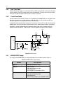
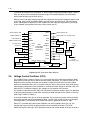
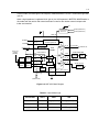
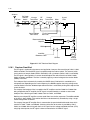
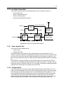
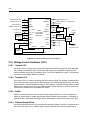
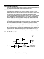
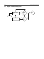
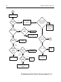
1
contact
contact
control
control
C
A, Motorola, Professional Radio, PRO Series and PRO Model
numbers and HT Series and HT Model numbers are marks of
Motorola, Inc. LTR is a registered trademark of E.F. Johnson
Company. Transcrypt is a registered trademark of Transcrypt
International, Inc. PassPort is a registered trademark of Trident
Micro Systems, Inc.
© 2000, 2001 Motorola, Inc. All rights reserved. Printed in U.S.A.
*6881088C46*
68P81088C46-D
Detailed
Service Manual
Professional Radio
Portable Radios
Safety-i
SAFETY AND GENERAL INFORMATION
IMPORTANT INFORMATION ON SAFE AND EFFICIENT OPERATION
READ THIS INFORMATION BEFORE USING YOUR TWO-WAY RADIO
The information provided in this document supersedes the general safety information contained in user
guides published prior to July 2000. For information regarding radio use and hazardous atmosphere please
refer to the Factory Mutual (FM) Approval Manual Supplement or Instruction Card, which is included with
radio models that offer this capability.
RF Operational Characteristics
Your radio contains a transmitter and a receiver. When it is ON, it receives and transmits radio frequency (RF)
energy.
Exposure To Radio Frequency Energy
Your Motorola Two-Way Radio, is designed to comply with the following National and International Standards and
Guidelines regarding exposure of human beings to radio frequency electromagnetic energy (EME):
•
United States Federal Communications Commission, Code of Federal Regulations
(47 CFR part 2 sub-part J).
•
American National Standards Institute (ANSI)/Institute of Electrical and Electronic Engineers (IEEE)
(C95.1 - 1992)
•
Institute of Electrical and Electronic Engineers (IEEE) (C95.1-1999 Edition)
•
National Council on Radiation Protection and Measurements (NCRP) of the United States (Report 86,
1986)
•
International Commission on Non-Ionizing Radiation Protection (ICNRP - 1998)
•
National Radiological Protection Board of the United Kingdom (1995)
•
Ministry of Health (Canada) Safety Code 6. Limits of Human Exposure to Radio frequency Electromagnetic
Fields in the Frequency Range from 3 kHz to 300 GHz (1999)
•
Australian Communications Authority Radiocommunications (Electromagnetic Radiation - Human Exposure) Standard (1999) (applicable to wireless phones only)
PORTABLE RADIO OPERATION AND EME EXPOSURE
To assure optimal radio performance and make sure human exposure to radio frequency electromagnetic
energy is within the guidelines set forth in the above standards, always adhere to the following procedures:
Antenna Care
Use only the supplied or an approved replacement antenna. Unauthorized antennas, modifications, or
attachments could damage the radio and may violate FCC regulations.
DO NOT hold the antenna when the two-way radio is “IN USE”. Holding the antenna affects call quality
and may cause the radio to operate at a higher power level than needed.
Two-Way Radio Operation
When using your radio as a traditional two-way radio, hold the radio in a vertical position with the
microphone one to two inches (2.5 to 5 cm) away from the lips.
MAN WITH RADIO
Safety-ii
Body-Worn Operation
To maintain compliance with FCC RF exposure guidelines, if you wear a radio on your body when
transmitting, always place the radio in a Motorola supplied or approved clip, holder, holster, case, or
body harness. Use of non-Motorola-approved accessories may exceed FCC RF exposure guidelines. If you
do not use a body-worn accessory, ensure the antenna is at least one inch (2.5 cm) from your body
when transmitting.
Data Operation
When using any data feature of the radio, with or without an accessory cable, position the antenna of the
radio at least one inch (2.5 cm) from the body.
ELECTROMAGNETIC INTERFERENCE/COMPATIBILITY
Note: Nearly every electronic device is susceptible to electromagnetic interference (EMI) if inadequately
shielded, designed or otherwise configured for electromagnetic compatibility.
• FACILITIES
To avoid electromagnetic interference and/or compatibility conflicts, turn off your radio in any facility where
posted notices instruct you to do so. Hospitals or health care facilities may be using equipment that is
sensitive to external RF energy.
•
AIRCRAFT
When instructed to do so, turn off your radio when on board an aircraft. Any use of a radio must be in
accordance with applicable regulations per airline crew instructions.
•
MEDICAL DEVICES
• Pacemakers
The Health Industry Manufacturers Association recommends that a minimum separation of 6 inches (15
cm) be maintained between a handheld wireless radio and a pacemaker. These recommendations are
consistent with the independent research by, and recommendations of, Wireless Technology Research.
Persons with pacemakers should:
•
•
•
•
ALWAYS keep the radio more than six inches (15 cm) from their pacemaker when the radio is turned ON.
not carry the radio in the breast pocket.
use the ear opposite the pacemaker to minimize the potential for interference.
turn the radio OFF immediately if you have any reason to suspect that interference is taking place.
• Hearing Aids
Some digital wireless radios may interfere with some hearing aids. In the event of such interference, you
may want to consult your hearing aid manufacturer to discuss alternatives.
• Other Medical Devices
If you use any other personal medical device, consult the manufacturer of your device to determine if it is
adequately shielded from RF energy. Your physician may be able to assist you in obtaining this
information.
Safety-iii
SAFETY AND GENERAL
•
Use While Driving
Check the laws and regulations on the use of radios in the area where you drive. Always obey them
When using your radio while driving, please:
•
Give full attention to driving and to the road.
•
Use hands-free operation, if available.
•
Pull off the road and park before making or answering a call if driving conditions so require.
OPERATIONAL WARNINGS
•
FOR VEHICLES WITH AN AIR BAG
!
WARNING
Do not place a portable radio in the area over an air bag or in the air bag deployment area. Air bags inflate
with great force. If a portable radio is placed in the air bag deployment area and the air bag inflates, the radio
may be propelled with great force and cause serious injury to occupants of the vehicle.
•
POTENTIALLY EXPLOSIVE ATMOSPHERES
Turn off your radio prior to entering any area with a potentially explosive atmosphere, unless it is a radio type
especially qualified for use in such areas as “Intrinsically Safe” (for example, Factory Mutual, CSA, or UL
Approved). Do not remove, install, or charge batteries in such areas. Sparks in a potentially explosive
atmosphere can cause an explosion or fire resulting in bodily injury or even death.
Note: The areas with potentially explosive atmospheres referred to above include fueling areas such as
below decks on boats, fuel or chemical transfer or storage facilities, areas where the air contains
chemicals or particles, such as grain, dust or metal powders, and any other area where you would normally be advised to turn off your vehicle engine. Areas with potentially explosive atmospheres are
often but not always posted.
•
BLASTING CAPS AND AREAS
To avoid possible interference with blasting operations, turn off your radio when you are near electrical
blasting caps, in a blasting area, or in areas posted: “Turn off two-way radio”. Obey all signs and instructions.
OPERATIONAL CAUTIONS
•
ANTENNAS
!
Caution
Do not use any portable radio that has a damaged antenna. If a damaged antenna comes into contact
with your skin, a minor burn can result.
•
BATTERIES
All batteries can cause property damage and/or bodily injury such as burns if a conductive material such as
jewelry, keys, or beaded chains touch exposed terminals. The conductive material may complete an electrical
circuit (short circuit) and become quite hot. Exercise care in handling any charged battery, particularly when
placing it inside a pocket, purse, or other container with metal objects.
Safety-iv
Intrinsically Safe Radio Information
FMRC Approved Equipment
Anyone intending to use a radio in a location where hazardous concentrations of flammable material
exist (hazardous atmosphere) is advised to become familiar with the subject of intrinsic safety and
with the National Electric Code NFPA 70 (National Fire Protection Association) Article 500 (hazardous
[classified] locations).
An Approval Guide, issued by Factory Mutual Research Corporation (FMRC), lists manufacturers and
the products approved by FMRC for use in such locations. FMRC has also issued a voluntary
approval standard for repair service (“Class Number 3605”).
FMRC Approval labels are attached to the radio to identify the unit as being FM Approved for
specified hazardous atmospheres. This label specifies the hazardous Class/Division/Group along
with the part number of the battery that must be used. Depending on the design of the portable unit,
this FM label can be found on the back of the radio housing or the bottom of the radio housing.Their
Approval mark is shown below.
FM
APPROVED
!
WARNING: Do not operate radio communications equipment in a hazardous atmosphere
unless it is a type especially qualified (e.g. FMRC Approved) for such use. An explosion or
fire may result.
WARNING: Do not operate the FMRC Approved Product in a hazardous atmosphere if it has
been physically damaged (e.g. cracked housing). An explosion or fire may result.
WARNING: Do not replace or charge batteries in a hazardous atmosphere. Contact sparking
may occur while installing or removing batteries and cause an explosion or fire.
WARNING: Do not replace or change accessories in a hazardous atmosphere. Contact
sparking may occur while installing or removing accessories and cause an explosion or fire.
WARNING: Do not operate the FMRC Approved Product unit in a hazardous location with the
accessory contacts exposed. Keep the connector cover in place when accessories are not
used.
WARNING: Turn radio off before removing or installing a battery or accessory.
WARNING: Do not disassemble the FMRC Approved Product unit in any way that exposes
the internal electrical circuits of the unit.
Radios must ship from the Motorola manufacturing facility with the hazardous atmosphere
capability and FM Approval labeling. Radios will not be “upgraded” to this capability and
labeled in the field.
A modification changes the unit’s hardware from its original design configuration. Modifications can
only be done by the original product manufacturer at one of its FMRC audited manufacturing facilities.
!
WARNING: Failure to use an FMRC Approved Product unit with an FMRC Approved battery
or FMRC Approved accessories specifically approved for that product may result in the dangerously unsafe condition of an unapproved radio combination being used in a hazardous
location.
Unauthorized or incorrect modification of an FMRC Approved Product unit will negate the Approval
rating of the product.
Safety-v
Repair of FMRC Approved Products
REPAIRS FOR MOTOROLA FMRC APPROVED PRODUCTS ARE THE RESPONSIBILITY OF THE
USER.
You should not repair or relabel any Motorola manufactured communication equipment bearing the
FMRC Approval label (FMRC Approved Product) unless you are familiar with the current FMRC
Approval standard for repairs and service (Class Number 3605).
You may want to consider using a repair facility that operates under 3605 repair service approval.
!
WARNING: Incorrect repair or relabeling of any FMRC Approved Product unit could
adversely affect the Approval rating of the unit.
WARNING: Use of a radio that is not intrinsically safe in a hazardous atmosphere could
result in serious injury or death.
FMRC’s Approval Standard Class Number 3605 is subject to change at any time without notice to
you, so you may want to obtain a current copy of 3605 from FMRC. Per the December, 1994
publication of 3605, some key definitions and service requirements are as follows:
Repair
A repair constitutes something done internally to the unit that would bring it back to its original
condition Approved by FMRC. A repair should be done in an FMRC Approved facility.
Items not considered as repairs are those in which an action is performed on a unit which does not
require the outer casing of the unit to be opened in a manner which exposes the internal electrical
circuits of the unit. You do not have to be an FMRC Approved Repair Facility to perform these actions.
Relabeling
The repair facility shall have a method by which the replacement of FMRC Approval labels are
controlled to ensure that any relabeling is limited to units that were originally shipped from the
Manufacturer with an FM Approval label in place. FMRC Approval labels shall not be stocked by the
repair facility. An FMRC Approval label shall be ordered from the original manufacturer as needed to
repair a specific unit. Replacement labels may be obtained and applied by the repair facility providing
satisfactory evidence that the unit being relabeled was originally an FMRC Approved unit. Verification
may include, but is not limited to: a unit with a damaged Approval label, a unit with a defective housing
displaying an Approval label, or a customer invoice indicating the serial number of the unit and
purchase of an FMRC Approved model.
Do Not Substitute Options or Accessories
The Motorola communications equipment certified by Factory Mutual is tested as a system and
consists of the FM Approved portable, FM Approved battery, and FM Approved accessories or
options, or both. This Approved portable and battery combination must be strictly observed. There
must be no substitution of items, even if the substitute has been previously Approved with a different
Motorola communications equipment unit. Approved configurations are listed in the FM Approval
guide published by FMRC, or in the product FM Supplement. This FM Supplement is shipped with FM
Approved radio and battery combination from the manufacturer. The Approval guide, or the Approval
standard Class Number 3605 document for repairs and service, can be ordered directly through
Factory Mutual Research Corporation located in Norwood, Massachusetts.
Safety-vi
This page intentionally left blank.
vii
Table of Contents
Chapter 1
1.1
1.2
Scope of Manual ........................................................................................................... 1-1
Warranty and Service Support..................................................................................... 1-1
1.2.1
1.2.2
1.2.3
1.3
1.4
Warranty Period................................................................................................................... 1-1
Return Instructions .............................................................................................................. 1-1
After Warranty Period .......................................................................................................... 1-1
Related Documents ...................................................................................................... 1-2
Technical Support......................................................................................................... 1-2
1.4.1
1.5
1.6
Introduction
Piece Parts Availability ........................................................................................................ 1-2
Radio Model Chart and Specifications........................................................................ 1-3
Radio Model Information .............................................................................................. 1-3
Chapter 2
Theory of Operation
2.1
2.2
Introduction ................................................................................................................... 2-1
Radio Power Distribution ............................................................................................. 2-1
Figure 2-1:DC Power Distribution Block Diagram ............................................................. 2-1
2.3 Keypad ........................................................................................................................... 2-2
Figure 2-2:Keypad Block Diagram .................................................................................... 2-2
2.4 Controller Board ........................................................................................................... 2-3
Figure 2-3:Controller Block Diagram................................................................................. 2-3
2.4.1
2.4.1
2.4.2
MCU Digital ......................................................................................................................... 2-3
Real Time Clock .................................................................................................................. 2-4
Circuit Description ............................................................................................................... 2-4
Figure 2-4:RTC Circuit ...................................................................................................... 2-4
2.4.1
2.4.1
2.5
UHF Transmitter ............................................................................................................ 2-5
Figure 2-5:UHF Transmitter Block Diagram...................................................................... 2-5
2.5.1
2.5.2
2.5.3
2.5.4
2.5.5
2.5.6
2.6
MODB/VSTBY Supply ......................................................................................................... 2-4
Audio/Signaling.................................................................................................................... 2-5
Power Amplifier (PA) ........................................................................................................... 2-5
Antenna Switch.................................................................................................................... 2-6
Harmonic Filter .................................................................................................................... 2-6
Antenna Matching Network ................................................................................................. 2-6
Power Control Integrated Circuit (PCIC) ............................................................................. 2-6
Temperature Cut Back Circuit ............................................................................................. 2-6
UHF Receiver................................................................................................................. 2-6
Figure 2-6:UHF Receiver Block Diagram.......................................................................... 2-7
2.6.1
2.6.2
2.6.3
2.6.4
Receiver Front-End ............................................................................................................. 2-7
Receiver Back-End.............................................................................................................. 2-8
Automatic Gain Control (AGC) ............................................................................................ 2-8
Frequency Generation Circuit.............................................................................................. 2-9
Figure 2-7:UHF Frequency Generation Unit Block Diagram............................................. 2-9
Synthesizer .................................................................................................................... 2-9
Figure 2-8:UHF Synthesizer Block Diagram ................................................................... 2-10
2.8 Voltage Control Oscillator (VCO)............................................................................... 2-10
Figure 2-9:UHF VCO Block Diagram .............................................................................. 2-11
2.7
viii
2.9
VHF Transmitter .......................................................................................................... 2-12
Figure 2-10:VHF Transmitter Block Diagram.................................................................. 2-12
2.9.1
2.9.2
2.9.3
2.9.4
2.9.5
Power Amplifier.................................................................................................................. 2-12
Antenna Switch.................................................................................................................. 2-12
Harmonic Filter .................................................................................................................. 2-13
Antenna Matching Network................................................................................................ 2-13
Power Control Integrated Circuit (PCIC)............................................................................ 2-13
2.10 VHF Receiver............................................................................................................... 2-13
Figure 2-11:VHF Receiver Block Diagram...................................................................... 2-14
2.10.1
2.10.2
2.10.3
2.10.4
Receiver Front-End............................................................................................................ 2-14
Receiver Back-End ............................................................................................................ 2-15
Automatic Gain Control (AGC) .......................................................................................... 2-15
Frequency Generation Circuit............................................................................................ 2-16
Figure 2-12:VHF Frequency Generation Unit Block Diagram......................................... 2-16
2.11 Synthesizer.................................................................................................................. 2-16
Figure 2-13:VHF Synthesizer Block Diagram ................................................................. 2-17
2.12 Voltage Control Oscillator (VCO) .............................................................................. 2-17
Figure 2-14:VHF VCO Block Diagram ............................................................................ 2-18
2.13 Low Band Transmitter ................................................................................................ 2-19
Figure 2-15:Low Band Transmitter Block Diagram ......................................................... 2-19
2.13.1
2.13.2
2.13.3
2.13.4
2.13.5
2.13.6
2.13.7
Power Amplifier (PA) ......................................................................................................... 2-19
Antenna Switch.................................................................................................................. 2-19
Harmonic Filter .................................................................................................................. 2-20
Antenna Matching Transformer ......................................................................................... 2-20
Power Control Integrated Circuit (PCIC)............................................................................ 2-20
Temperature Cut Back Circuit ........................................................................................... 2-20
Electrostatic Discharge (ESD) Protection Circuit............................................................... 2-20
2.14 Low Band Receiver..................................................................................................... 2-20
Figure 2-16:Low Band Receiver Block Diagram ............................................................. 2-21
2.14.1
2.14.2
2.14.3
2.14.4
Receiver Front-End............................................................................................................ 2-21
Receiver Back-End ............................................................................................................ 2-22
Automatic Gain Control (AGC) .......................................................................................... 2-22
Frequency Generation Circuit............................................................................................ 2-22
Figure 2-17:Low Band Frequency Generation Unit Block Diagram ................................ 2-23
2.15 Synthesizer.................................................................................................................. 2-23
Figure 2-18:Low Band Synthesizer Block Diagram ........................................................ 2-24
2.16 Voltage Control Oscillators (VCO) ............................................................................ 2-24
2.16.1
2.16.2
2.16.3
2.16.4
2.16.5
Receive VCO ..................................................................................................................... 2-24
Transmit VCO .................................................................................................................... 2-24
Buffer ................................................................................................................................. 2-24
Diplexer/Output Filters ....................................................................................................... 2-24
Prescalar Feedback........................................................................................................... 2-25
2.17 800 MHz Transmitter................................................................................................... 2-25
Figure 2-19:800 MHz Transmitter Block Diagram........................................................... 2-25
2.17.1
2.17.2
2.17.3
2.17.4
Power Amplifier.................................................................................................................. 2-25
Antenna Switch.................................................................................................................. 2-26
Harmonic Filter .................................................................................................................. 2-26
Power Control Integrated Circuit (PCIC)............................................................................ 2-26
2.18 800 MHz Receiver ....................................................................................................... 2-27
Figure 2-20:800MHz Receiver Block Diagram ............................................................... 2-27
2.18.1 Receiver Front-End............................................................................................................ 2-27
2.18.2 Receiver Back-End ............................................................................................................ 2-28
ix
2.18.3 Automatic Gain Control Circuit .......................................................................................... 2-28
2.18.4 Frequency Generation Circuit............................................................................................ 2-29
Figure 2-21:800 MHz Frequency Generation Unit Block Diagram.................................. 2-29
2.19 Synthesizer .................................................................................................................. 2-30
Figure 2-22:800 MHz Synthesizer Block Diagram .......................................................... 2-30
2.19.1 Voltage Control Oscillator (VCO)....................................................................................... 2-31
Figure 2-23:800 MHz VCO Block Diagram ..................................................................... 2-31
2.20 Trunked Radio Systems ............................................................................................. 2-32
2.20.1
2.20.2
2.20.3
2.20.4
Privacy Plus Trunked Systems.......................................................................................... 2-32
LTR™ Trunked Systems ................................................................................................... 2-32
MPT Trunked Systems ...................................................................................................... 2-32
PassPort™ Trunked Systems ........................................................................................... 2-33
2.21 900 MHz Transmitter ................................................................................................... 2-34
Figure 2-24:Transmitter Block Diagram .......................................................................... 2-34
2.21.1
2.21.2
2.21.3
2.21.4
Power Amplifier ................................................................................................................. 2-35
Antenna Switch.................................................................................................................. 2-35
Harmonic Filter .................................................................................................................. 2-35
Power Control Integrated Circuit (PCIC) ........................................................................... 2-35
2.22 900 MHz Receiver........................................................................................................ 2-36
Figure 2-25:900 MHz Receiver Block Diagram............................................................... 2-36
2.22.1
2.22.2
2.22.3
2.22.4
Receiver Front-End ........................................................................................................... 2-36
Receiver Back-End............................................................................................................ 2-37
Hear Clear IC..................................................................................................................... 2-37
Automatic Gain Control Circuit .......................................................................................... 2-38
2.23 Frequency Generation Circuitry ................................................................................ 2-39
Figure 2-26:Frequency Generation Unit Block Diagram ................................................. 2-39
2.24 900 MHz Synthesizer .................................................................................................. 2-40
Figure 2-27:Synthesizer Block Diagram.......................................................................... 2-40
2.25 900 MHz Voltage Control Oscillator (VCO) ............................................................... 2-41
Figure 2-28:VCO Block Diagram..................................................................................... 2-41
Chapter 3
3.1
3.3
Maintenance
Introduction ................................................................................................................... 3-1
Inspection ...................................................................................................................... 3-1
3.3.1
Cleaning .............................................................................................................................. 3-1
3.4
3.5
3.6
3.7
Safe Handling of CMOS and LDMOS........................................................................... 3-2
General Repair Procedures and Techniques ............................................................. 3-2
Recommended Test Tools ........................................................................................... 3-4
Replacing the Circuit Board Fuse ............................................................................... 3-5
Figure 3-1:UHF/VHF/Low Band/800MHz/900MHz Circuit Board Fuse Locations ............ 3-6
3.2 Removing and Reinstalling the Circuit Board............................................................ 3-7
Figure 3-2:Circuit Board Removal and Reinstallation ....................................................... 3-7
3.3 Power Up Self-Test Error Codes.................................................................................. 3-7
3.4 UHF Troubleshooting Charts ....................................................................................... 3-9
Troubleshooting Flow Chart for Controller........................................................................................ 3-9
Troubleshooting Flow Chart for Receiver (Sheet 1 of 2) ................................................................ 3-10
Troubleshooting Flow Chart for Receiver (Sheet 2 of 2) ................................................................ 3-11
Troubleshooting Flow Chart for Transmitter ................................................................................... 3-12
Troubleshooting Flow Chart for Synthesizer .................................................................................. 3-13
Troubleshooting Flow Chart for VCO ............................................................................................. 3-14
x
3.5
VHF Troubleshooting Charts ..................................................................................... 3-15
Troubleshooting Flow Chart for Controller ...................................................................................... 3-15
Troubleshooting Flow Chart for Receiver (Sheet 1 of 2) ................................................................ 3-16
Troubleshooting Flow Chart for Receiver (Sheet 2 of 2) ................................................................ 3-17
Troubleshooting Flow Chart for Transmitter ................................................................................... 3-18
Troubleshooting Flow Chart for Synthesizer................................................................................... 3-19
Troubleshooting Flow Chart for VCO.............................................................................................. 3-20
3.6
Low Band Troubleshooting Charts ........................................................................... 3-21
Troubleshooting Flow Chart for Controller ...................................................................................... 3-21
Troubleshooting Flow Chart for Receiver (Sheet 1 of 2) ................................................................ 3-22
Troubleshooting Flow Chart for Receiver (Sheet 2 of 2) ................................................................ 3-23
Troubleshooting Flow Chart for Transmitter ................................................................................... 3-24
Troubleshooting Flow Chart for Synthesizer................................................................................... 3-25
Troubleshooting Flow Chart for VCO.............................................................................................. 3-26
3.7
800 MHz Troubleshooting Charts.............................................................................. 3-27
Troubleshooting Flow Chart for Controller ...................................................................................... 3-27
Troubleshooting Flow Chart for Receiver (Sheet 1 of 2) ................................................................ 3-28
Troubleshooting Flow Chart for Receiver (Sheet 2 of 2) ................................................................ 3-29
Troubleshooting Flow Chart for Transmitter ................................................................................... 3-30
Troubleshooting Flow Chart for Synthesizer................................................................................... 3-31
Troubleshooting Flow Chart for VCO.............................................................................................. 3-32
3.8 PassPort Trunking Troubleshooting Chart .............................................................. 3-33
3.9 Keypad Troubleshooting Chart ................................................................................. 3-34
3.10 900 MHz Troubleshooting Charts.............................................................................. 3-35
Troubleshooting Flow Chart for Controller (Sheet 1 of 2) ............................................................... 3-35
Troubleshooting Flow Chart for Controller (Sheet 2 of 2) ............................................................... 3-36
Troubleshooting Flow Chart for Receiver (Sheet 1 of 2) ................................................................ 3-37
Troubleshooting Flow Chart for Receiver (Sheet 2 of 2) ................................................................ 3-38
Troubleshooting Flow Chart for Transmitter ................................................................................... 3-39
Troubleshooting Flow Chart for Synthesizer................................................................................... 3-40
Troubleshooting Flow Chart for VCO.............................................................................................. 3-40
Chapter 4
4.1
Introduction ................................................................................................................... 4-1
4.1.1
4.2
Schematic Diagrams, Overlays, and Parts Lists
Notes For All Schematics and Circuit Boards...................................................................... 4-1
Flex Layout .................................................................................................................... 4-2
Figure 4-1:Keypad-Controller Interconnect Flex ............................................................... 4-2
4.2.1
Keypad-Controller Interconnect Flex Schematic ................................................................. 4-3
Figure 4-2:Keypad-Controller Interconnect Flex Schematic Diagram............................... 4-3
4.2.2
4.2.3
Keypad-Controller Interconnect Flex Parts List ................................................................... 4-3
Universal Flex Connector ................................................................................................... 4-4
Figure 4-3:Universal Flex Connector ................................................................................ 4-4
4.2.4
Universal Connector Flex Schematic................................................................................... 4-5
Figure 4-4:Universal Flex Connector Schematic Diagram................................................ 4-5
4.2.5
4.2.6
Universal Flex Connector Parts List .................................................................................... 4-5
Keypad Top and Bottom Overlays....................................................................................... 4-6
Figure 4-5:Keypad Top and Bottom Board Overlays ........................................................ 4-6
Figure 4-6:Keypad Board (5000 and 7000 Series) Schematic Diagram.......................... 4-7
Figure 4-7:9000 Series Keypad Top and Bottom Board Overlays................................... 4-9
Figure 4-8:9000 Series Keypad Board Schematic Diagram ........................................... 4-10
xi
Figure 4-9:VHF/UHF Complete Controller Schematic Diagram......................................
Figure 4-10:VHF/UHF Controller ASFIC/ON_OFF Schematic Diagram .........................
Figure 4-11: VHF/UHF Controller ASFIC/ON_OFF Schematic Diagram ........................
Figure 4-12:VHF/UHF Controller Micro Processor Schematic Diagram .........................
Figure 4-13:VHF/UHF Controller Micro Processor Schematic Diagram .........................
Figure 4-14:Controller Memory Schematic Diagram.......................................................
Figure 4-15:Controller Audio Power Amplifier Schematic Diagram ................................
Figure 4-16:Controller Interface Schematic Diagram......................................................
Figure 4-17:UHF (403-470MHz) 5000/7000 Series Main Board Top Side
PCB 8480450Z03............................................................................................................
Figure 4-18:UHF (403-470MHz) 5000/7000 Series Main Board Bottom Side
PCB 8480450Z03............................................................................................................
Figure 4-19:UHF (403-470MHz) 5000/7000 Series Main Board Top Side
PCB 8480450Z13............................................................................................................
Figure 4-20:UHF (403-470MHz) 5000/7000 Series Main Board Bottom Side
PCB 8480450Z13............................................................................................................
Figure 4-21:UHF (403-470MHz) Controls and Switches Schematic Diagram ................
Figure 4-22:UHF (403-470MHz) Receiver Front End Schematic Diagram .....................
Figure 4-23:UHF (403-470MHz) Receiver Back End Schematic Diagram .....................
Figure 4-24:UHF (403-470MHz) Synthesizer Schematic Diagram .................................
Figure 4-25:UHF (403-470MHz) Voltage Controlled Oscillator Schematic Diagram ......
Figure 4-26:UHF (403-470MHz) Transmitter Schematic Diagram..................................
Figure 4-27:UHF (403-470MHz) 9000 Series Main Board Top Side PCB ......................
Figure 4-28:UHF (403-470MHz) 9000 Series Main Board Bottom Side PCB.................
Figure 4-29:UHF (403-470MHz) Controls and Switches Schematic Diagram ................
Figure 4-30:UHF (403-470MHz) Receiver Front End Schematic Diagram .....................
Figure 4-31:UHF (403-470MHz) Receiver Back End Schematic Diagram .....................
Figure 4-32:UHF (403-470MHz) Synthesizer Schematic Diagram .................................
Figure 4-33:UHF (403-470MHz) Voltage Controlled Oscillator Schematic Diagram ......
Figure 4-34:UHF (403-470MHz) Transmitter Schematic Diagram..................................
Figure 4-35:UHF (450-527MHz) 5000/7000 Series Main Board Top Side
PCB 8485641Z02............................................................................................................
Figure 4-36:UHF (450-527MHz) 5000/7000 Series Main Board Bottom Side
PCB 8485641Z02............................................................................................................
Figure 4-37:UHF (450-527MHz) 5000/7000 Series Main Board Top Side
PCB 8485641Z06............................................................................................................
Figure 4-38:UHF (450-527MHz) 5000/7000 Series Main Board Bottom Side
PCB 8485641Z06............................................................................................................
Figure 4-39:UHF (450-527MHz) Controls and Switches Schematic Diagram ................
Figure 4-40:UHF (450-527MHz) Receiver Front End Schematic Diagram .....................
Figure 4-41:UHF (450-527MHz) Receiver Back End Schematic Diagram .....................
Figure 4-42:UHF (450-527MHz) Synthesizer Schematic Diagram .................................
Figure 4-43:UHF (450-527MHz) Voltage Controlled Oscillator Schematic Diagram ......
Figure 4-44:UHF (450-527MHz) Transmitter Schematic Diagram..................................
Figure 4-45:UHF (450-527MHz) 9000 Series Main Board Top Side PCB ......................
Figure 4-46:UHF (450-527MHz) 9000 Series Main Board Bottom Side PCB.................
Figure 4-47:UHF (450-527MHz) Controls and Switches Schematic Diagram ................
Figure 4-48:UHF (450-527MHz) Receiver Front End Schematic Diagram .....................
Figure 4-49:UHF (450-527MHz) Receiver Back End Schematic Diagram .....................
Figure 4-50:UHF (450-527MHz) Synthesizer Schematic Diagram .................................
4-13
4-14
4-15
4-16
4-17
4-18
4-19
4-20
4-21
4-22
4-23
4-24
4-25
4-26
4-27
4-28
4-29
4-30
4-39
4-40
4-41
4-42
4-43
4-44
4-45
4-46
4-51
4-52
4-53
4-54
4-55
4-56
4-57
4-58
4-59
4-60
4-69
4-70
4-71
4-72
4-73
4-74
xii
Figure 4-51:UHF (450-527MHz) Voltage Controlled Oscillator Schematic Diagram ...... 4-75
Figure 4-52:UHF (450-527MHz) Transmitter Schematic Diagram.................................. 4-76
Figure 4-53:UHF (450-527MHz) Voice Storage Schematic Diagram ............................. 4-77
Figure 4-54:VHF (136-174MHz) Main Board Top Side PCB 8486062B09..................... 4-83
Figure 4-55:VHF (136-174MHz) Main Board Bottom Side PCB 8486062B09................ 4-84
Figure 4-56:VHF (136-174MHz) Controls and Switches Schematic Diagram ............... 4-85
Figure 4-57:VHF (136-174MHz)Receiver Front End Schematic Diagram ..................... 4-86
Figure 4-58:VHF (136-174MHz)Receiver Back End Schematic Diagram ...................... 4-87
Figure 4-59:VHF (136-174MHz)Synthesizer Schematic Diagram ................................. 4-88
Figure 4-60:VHF (136-174MHz)Voltage Controlled Oscillator Schematic Diagram ....... 4-89
Figure 4-61:VHF (136-174MHz)Transmitter Schematic Diagram................................... 4-90
Figure 4-62:VHF (136-174MHz) 5000/7000 Series Main Board Top Side
PCB 8486062B12 ........................................................................................................... 4-95
Figure 4-63:VHF (136-174MHz) 5000/7000 Series Main Board Bottom Side
PCB 8486062B12 ........................................................................................................... 4-96
Figure 4-64:VHF (136-174MHz) 5000/7000 Series Main Board Top Side
PCB 8486062B16 ........................................................................................................... 4-97
Figure 4-65:VHF (136-174MHz) 5000/7000 Series Main Board Bottom Side
PCB 8486062B16 ........................................................................................................... 4-98
Figure 4-66:VHF (136-174MHz) Controls and Switches Schematic Diagram ................ 4-99
Figure 4-67:VHF (136-174MHz) Receiver Front End Schematic Diagram ................... 4-100
Figure 4-68:VHF (136-174MHz) Receiver Back End Schematic Diagram ................... 4-101
Figure 4-69:VHF (136-174MHz) Synthesizer Schematic Diagram ............................... 4-102
Figure 4-70:VHF (136-174MHz) Voltage Controlled Oscillator Schematic Diagram .... 4-103
Figure 4-71:VHF (136-174MHz) Transmitter Schematic Diagram................................ 4-104
Figure 4-72:VHF (136-174MHz) 9000 Series Main Board Top Side PCB .................... 4-113
Figure 4-73:VHF (136-174MHz) 9000 Series Main Board Bottom Side PCB............... 4-114
Figure 4-74:VHF (136-174MHz) Controls and Switches Schematic Diagram .............. 4-115
Figure 4-75:VHF (136-174MHz) Receiver Front End Schematic Diagram ................... 4-116
Figure 4-76:VHF (136-174MHz) Receiver Back End Schematic Diagram ................... 4-117
Figure 4-77:VHF (136-174MHz) Synthesizer Schematic Diagram ............................... 4-118
Figure 4-78:VHF (136-174MHz) Voltage Controlled Oscillator Schematic Diagram .... 4-119
Figure 4-79:VHF (136-174MHz) Transmitter Schematic Diagram................................ 4-120
Figure 4-80:Low Band (29.7-42/35-50MHz) Main Board Top Side PCB ...................... 4-125
Figure 4-81:Low Band (29.7-42/35-50MHz) Main Board Bottom Side PCB ................. 4-126
Figure 4-82:Low Band (30-50MHz) Controls and Switches Diagram ........................... 4-127
Figure 4-83:Low Band (29.7-42/35-50MHz) Controller Overall
Schematic Diagram....................................................................................................... 4-128
Figure 4-84:Low Band (29.7-42/35-50MHz) Controller Memory
Schematic Diagram....................................................................................................... 4-129
Figure 4-85:Low Band (29.7-42/35-50MHz) Controller AFSIC
Schematic Diagram....................................................................................................... 4-130
Figure 4-86:Low Band (29.7-42/35-50MHz) Controller Microprocessor
Schematic Diagram....................................................................................................... 4-131
Figure 4-87:Low Band (29.7-42/35-50MHz) Controller Audio PA
Schematic Diagram....................................................................................................... 4-132
Figure 4-88:Low Band (29.7-42/35-50MHz) Receiver Front End
Schematic Diagram....................................................................................................... 4-133
Figure 4-89:Low Band (29.7-42/35-50MHz) Receiver Back End
Schematic Diagram....................................................................................................... 4-134
xiii
Figure 4-90:Low Band (29.7-42/35-50MHz) Frequency Generation
Unit Synthesizer ............................................................................................................
Figure 4-91:Lowband (29.7-42/35-50MHz) Frequency Generation Unit
VCO Diagram................................................................................................................
Figure 4-92:Lowband (29.7-42/35-50MHz) Transmitter Schematic Diagram ...............
Figure 4-93:800MHz (806-870MHz) Main Board Top Side PCB 84860641Z02 ...........
Figure 4-94:800MHz (806-870MHz) Main Board Bottom Side PCB 84860641Z02......
Figure 4-95: 800MHz Popular/Preferred (806-870MHz) Main Board Top Side
PCB 8480641Z03 (Rev B) ............................................................................................
Figure 4-96:800MHz Popular/Preferred (806-870MHz) Main Board Bottom Side
PCB 8480641Z03 (Rev B) ............................................................................................
Figure 4-97:800MHz Complete Controller ....................................................................
Figure 4-98: 800MHz Controller ASFIC/ON_OFF.........................................................
Figure 4-99: 800MHz Controller Micro Processor.........................................................
Figure 4-100: 800MHz Controller Memory....................................................................
Figure 4-101: 800MHz Controller Audio Power Amplifier .............................................
Figure 4-102: 800MHz Controller Interface...................................................................
Figure 4-103:800MHz Controls and Switches Schematic Diagram ..............................
Figure 4-104:800MHz Receiver Front End Schematic Diagram ...................................
Figure 4-105:800MHz Receiver Back End Schematic Diagram ...................................
Figure 4-106:800MHz Synthesizer Schematic Diagram ...............................................
Figure 4-107:800MHz Voltage Controlled Oscillator Schematic Diagram ....................
Figure 4-108:800MHz Transmitter Schematic Diagram (Rev A) ..................................
Figure 4-109:800MHz Transmitter Schematic Diagram (Rev B) ..................................
Figure 4-110:PassPort Trunking Controller PCB Board Side 1 & 2 ..............................
Figure 4-111:PassPort Controller Schematic Diagram ................................................
Figure 4-112:900MHz (896-941MHz) Main Board Top Side PCB 8485910Z01 ...........
Figure 4-113:900MHz (896-941MHz) Main Board Bottom Side PCB 8485910Z01......
Figure 4-114:900MHz Complete Controller ..................................................................
Figure 4-115:900MHz Controller ASFIC/ON_OFF........................................................
Figure 4-116:900MHz Controller Microprocessor .........................................................
Figure 4-117:900MHz Controller Memory.....................................................................
Figure 4-118:900MHz Controller Audio Power Amplifier ..............................................
Figure 4-119:900MHz Controller Interface....................................................................
Figure 4-120:900MHz Controls and Switches Schematic Diagram ..............................
Figure 4-121:900MHz Receiver Front End Schematic Diagram ...................................
Figure 4-122:900MHz Receiver Back End Schematic Diagram ...................................
Figure 4-123:900MHz Synthesizer Schematic Diagram ...............................................
Figure 4-124:900MHz Hear/Clear Schematic Diagram.................................................
Figure 4-125:900MHz Voltage Controlled Oscillator Schematic Diagram ....................
Figure 4-126:900MHz Transmitter Schematic Diagram................................................
4-135
4-136
4-137
4-141
4-142
4-143
4-144
4-145
4-146
4-147
4-148
4-149
4-150
4-151
4-152
4-153
4-154
4-155
4-156
4-157
4-161
4-162
4-163
4-164
4-165
4-166
4-167
4-168
4-169
4-170
4-171
4-172
4-173
4-174
4-175
4-176
4-177
xiv
1-1
Chapter 1
Introduction
1.1
Scope of Manual
This manual is intended for use by service technicians familiar with similar types of equipment. It
contains service information required for the equipment described and is current as of the printing
date. Changes that occur after the printing date are incorporated by a complete manual revision or
alternatively, as additions.
NOTE Before operating or testing these units, please read the Safety Information Section in the
front of this manual.
1.2
Warranty and Service Support
Motorola offers long term support for its products. This support includes full exchange and/or repair of
the product during the warranty period, and service/repair or spare parts support out of warranty. Any
“return for exchange” or “return for repair” by an authorized Motorola dealer must be accompanied by
a warranty claim form. Warranty claim forms are obtained by contacting customer service.
1.2.1 Warranty Period
The terms and conditions of warranty are defined fully in the Motorola dealer or distributor or reseller
contract. These conditions may change from time to time and the following notes are for guidance
purposes only.
1.2.2 Return Instructions
In instances where the product is covered under a “return for replacement” or “return for repair”
warranty, a check of the product should be performed prior to shipping the unit back to Motorola. This
is to ensure that the product has been correctly programmed or has not been subjected to damage
outside the terms of the warranty.
Prior to shipping any radio back to a Motorola warranty depot, please contact the appropriate
customer service for instructions. All returns must be accompanied by a warranty claim form,
available from your customer services representative. Products should be shipped back in the original
packaging, or correctly packaged to ensure no damage occurs in transit.
1.2.3 After Warranty Period
After the Warranty period, Motorola continues to support its products in two ways:
First, Motorola's Accessories and Aftermarket Division (ADD) offers a repair service to both end users
and dealers at competitive prices.
Second, Motorola’s service department supplies individual parts and modules that can be purchased
by dealers who are technically capable of performing fault analysis and repair.
1-2
1.3
Related Documents
Related Documents
The following documents are directly related to the use and maintainability of this product.
Table 1-1
Title
Professional Radio Portable Level 1&2 Basic
Service Manual- English
Professional Radio Portable Level 1&2 Basic
Service Manual- Spanish
Professional Radio Portable Level 1&2 Basic
Service Manual- Portuguese
Professional Radio Portable Service Manual
Level 3 -English
Professional Radio Portable Service Manual
Level 3 -Spanish
Professional Radio Portable Service Manual
Level 3 -Portuguese
1.4
Part Number
68P81088C45
68P81088C47
68P81088C49
68P81088C46
68P81088C48
68P81088C50
Technical Support
Technical support is available to assist the dealer/distributor and self-maintained customers in
resolving any malfunction which may be encountered. Initial contact should be by telephone to
customer resources wherever possible. When contacting Motorola technical support, be prepared to
provide the product model number and the unit’s serial number. The contact locations and telephone
numbers are located in the Basic Service Manual listed under the Related Documents paragraph of
this chapter.
1.4.1 Piece Parts Availability
Some replacement parts, spare parts, and/or product information can be ordered directly. If a
complete Motorola part number is assigned to the part, and it is not identified as “Depot ONLY”, the
part is available from Motorola Accessories and Aftermarket Division (AAD). If no part number is
assigned, the part is not normally available from Motorola. If the part number is appended with an
asterisk, the part is serviceable by a Motorola depot only. If a parts list is not included, this generally
means that no user-serviceable parts are available for that kit or assembly.
Radio Model Chart and Specifications
Parts Order Entry
7:00 A. M. to 7:00 P. M. (Central Standard
Time)
Monday through Friday (Chicago, U. S. A.)
To Order Parts in the United States of
America:
1-800-422-4210, or 847-538-8023
1-800-826-1913, or 410-712-6200 (U. S.
Federal Government)
TELEX: 280127
FAX: 1-847-538-8198
FAX: 1-410-712-4991 (U. S. Federal
Government)
(U. S. A.) after hours or weekends:
1-800-925-4357
1-3
To Order Parts in Latin America and the
Caribbean:
1-847-538-8023
Motorola Parts
Accessories and Aftermarket Division
(United States and Canada)
Attention: Order Processing
1313 E. Algonquian Road
Schaumburg, IL 60196
Accessories and Aftermarket Division
Attention: Latin America and Caribbean
Order Processing
1313 E. Algonquian Road
Schaumburg, IL 60196
Parts Identification
1-847-538-0021 (Voice)
1-847-538-8194 (FAX)
1.5
Radio Model Chart and Specifications
The radio model charts and specifications are located in the Basic Service Manual listed under the
Related Documents paragraph of this chapter.
1.6
Radio Model Information
The model number and serial number are located on a label attached to the back of your radio. You
can determine the RF output power, frequency band, protocols, and physical packages from these
numbers. The example below shows one portable radio model number and its specific characteristics
1-4
Radio Model Information
.
Table 1-2 Radio Model Number
Example: AAH25KC9AA2 and LAH25KDC9AA3
Model
Series
H
25
H = Portable
AA or LA = Motorola Internal Use
AA
or
LA
Type
of Unit
Freq.
Band
Power
Level
Physical
Packages
Channel
Spacing
Protocol
Feature
Level
Model
Revision
Model
Package
A
N
K
C
C
9
AA
2
VHF
(136174MHz)
2.5W
No Display
Programmable
Conventional
2F for AA
4F for LA
R
D
D
6
DU
3
UHF1
(403470MHz)
4-5W
Keypad
25 kHz
LTR
16F
S
E
H
CK
5
UHF2
(450527MHz)
6W
1-Line Display
MPT
256F
LTR for
AA only
B
N
GB
6
Low Band,
R1 (29.742.0MHz)
4-Line Display
Privacy Plus
128F
256F
LTR
C
Low Band,
R2 (35.050.0MHz)
U
800MHz
(806-824)
(851869MHz)
GE
8
Privacy Plus
Roaming
160F
DP
PassPort
FC
Smart Zone
2-1
Chapter 2
Theory of Operation
2.1
Introduction
This chapter provides a detailed theory of operation for the radio components. Schematic diagrams
for the circuits described in the following paragraphs are located in Figures 4-1 through 4-120.
2.2
Radio Power Distribution
A block diagram of the DC power distribution throughout the radio board is shown in Figure 2-1. A
7.5V battery supplies the basic radio power (UNSWB) directly to the electronic on/off control, audio
power amplifier, 3.5V regulator, power amplifier automatic level control (ALC), and low battery detect
circuit. When the radio on/off/volume control is turned on, the switched SWB+ is applied to the various
radio power regulators, antenna switch, accessories 20-pin connector, keypad/option board, and
transmit LED. The Vdda signal from the 3.3V Vdda regulator supplies the microprocessor with
operating power. The Vdd regulator scheme is listed by band in Table 2-1. Data is then sent to the
controller ASFIC to turn on a DAC which takes over the momentary-on path within 12ms. The SWB+
signal supplies power until the radio is turned off. Jumpers for configuring the Vdda and Vddd
regulators are shown in Figure 2-1 and described in Table 2-2.
The radio turns off when either of the two following conditions occur:
•
•
Radio on/off/volume control is turned off.
Low battery condition is detected.
If a low battery level is detected by the microprocessor through either of the above conditions, the
radio personality data is stored to EEPROM prior to turning off.
Accessories
20 pin Connector
Keypad/Option Board
Prime Expansion Board
Audio
Power
Amplifier
4.0V/3.3V
UNSWB+
7.5V
Battery
SWB+
Fuse
MECH.
SWB+
3.5V
Reg.
LI Ion
Vdda
Regulator
Vdda
Vddd
Regulator
Vdda
Tx
Led
Control
Switching
Regulator
Int/Ext Vdd
MCU, ROM
and EEPROM
LCD
Driver
ASFIC_CMP
On/Off
Switch
5V
Regulator
Low Battery
Detect
PA, Driver
PCIC(ALC)
5V
Antenna
Switch
RF, AMP, IF AMP
Ext. RX.
Buffer (NU)
Figure 2-1: DC Power Distribution Block Diagram
FRACTN
VCOBIC
LVZIF
2-2
Table 2-1 VDD Regulator Scheme by Band
Vdd
Regulator
Scheme
Band
Low Band
Dual
VHF
Dual
UHF
Dual
800 MHz
Dual
900 MHz
Dual
Table 2-2 Radio Jumpers
Dual Vdd
Regulator
Scheme
Single Vdd
Regulator
Scheme
R401
Y
Y
R402
N
N
R403
N
Y
R404
N
N
R405
Y
N
Jumpers
R = Regulator Jumper
2.3
Keypad
The keypad block diagram is shown in Figure 2-2. The comparator compares the voltage when any
one of the keypad row or keypad column keys is pressed. Pressing a key sends a message to the
microprocessor through the output (KEY_INT) line signifying that a key has been pressed. The
microprocessor then samples the analog to digital voltages at the keypad row and keypad column,
then makes a comparison with a map table to identify the key pressed. Once the key is identified, a
corresponding message is displayed.
The LED_EN is set by the codeplug. When the value is set to low, the LED lights up during power up.
A high codeplug setting disables this feature.
Keypad Column
Data
Display
18 Pin
Connector
40 Pin Connector
Keypad
Row
Key_Int
LED
Comparator
Figure 2-2: Keypad Block Diagram
Keypad
Button
2-3
2.4
Controller Board
The controller board is the central interface between the various radio functions. It is separated into
MCU digital and audio/signalling functions as shown in Figure 2-3.
To Synthesizer
External
Microphone
Mod Out
Internal
Microphone
16.8 / 17.0 MHz
Reference Clock
from Synthesizer
Audio/Signalling
Recovered Audio
Squelch
External
Speaker
Audio Power
Amplifier/Filter
ASFIC
Internal
Speaker
3.3V
Regulator
(Vdda)
To RF Board
SPI
CLK
MCU Digital
SCI to Side
Connector
Microcontroller
3.3V
Regulator
(Vddd)
EEPROM
ROM
RAM
Figure 2-3: Controller Block Diagram
2.4.1
MCU Digital
The digital portion of the controller consists of a microcontroller and associated EEPROM, RAM, and
ROM memories. Combinations of different size RAM and ROM are available to support various
application software. RAM supports 8KB and 32KB sizes. ROM supports 128KB, 256KB, and 512KB
sizes. Table 2-3 lists the ROM, RAM and EEPROM requirements for different radios.
Table 2-3 Radio Memory Requirements
FEATURE LEVEL
ROM (KB)
EXT RAM
(KB)
EEPROM
(KB)
AA,DU
2 or 3
128
-
8
AA,DU
6
128
-
16
CK, GB, GE, FC
-
512
32
16
PROTOCOL
2-4
2.4.1
Real Time Clock
Radios with displays support a real time clock (RTC) module for purposes of message time stamping
and time keeping. The RTC module resides in the microcontroller. The clock uses a back-up lithiumIon battery for operating power when the primary battery is removed.
2.4.2
Circuit Description
The RTC module circuit, shown in Figure 2-4, is powered by the MODB/VSTBY pin and PI6/PI7 from
the crystal oscillator circuit. A clock frequency of 38.4kHz from a crystal oscillator provides the
reference signal which is divided down to 1Hz in the processor.
As the RTC module is powered separately from the processor Vdd, the RTC is kept active through the
MODB/VSTBY pin which provides the lithium battery back-up power when the radio is switched off.
A MOSFET transistor (Q416) switches in the battery supply when Vdd is removed. Q416 also
provides isolation from BOOT_CTRL function. The 3.3V regulator charges the Lithium battery.
UNSWB+
Vddd
U410
R461
C435
VIN VOUT
3.3V
3
1 VSS
2
R460
C434
HC11FL0
MODA
MODB
1
Q416
4
2
3
PI6
FL401
38.4kHz
R420
OUT
2
3
C436
R419
LI_ION
1
R462
GND
R426
CR411
5
IN
R463
PI7
BOOT_CTRL
C437
TP405
TEST_POINT
Figure 2-4: RTC Circuit
2.4.1
MODB/VSTBY Supply
The supply to the MODB/VSTBY pin varies depending on the conditions listed in Table 2-4.
Table 2-4 MODB/VSTBY Supply Modes
Condition
Circuit Operation
Radio On
Vddd supply voltage via CR411
Radio Off
• Vddd turned off
• Q416 gate pulled low by R462
• Q416 switched on
• U410 supplies 3.2V to MODB_VSTBY
Primary battery removed
• Vddd turned off
• Q416 gate pulled low by R462
• Q416 switched on
• Lithium battery provides 3.2V to MODB_VSTBY
2-5
2.4.1
Audio/Signaling
The audio/signalling/filter/companding IC (ASFIC) and the audio power amplifier (Figure 2-3) form the
main components of the audio/signalling section of the controller board. Inputs include a 16.8 MHz
clock from the synthesizer, recovered audio and squelch, MCU control signals, and external or
internal microphones. Outputs include a microprocessor clock (CLK), modulator output to the
synthesizer, and amplified audio signals to an internal or external speaker.
2.5
UHF Transmitter
The UHF transmitter consists of the following basic circuits as shown in Figure 2-5.
•
•
•
•
Power amplifier (PA).
Antenna switch/harmonic filter.
Antenna matching network.
Power control integrated circuit (PCIC).
PCIC
Vcontrol
Vcontrol
Antenna
Matching
Network
Power Amplifier (PA)
From VCO
PA
Driver
PA Final
Stage
Antenna Switch/
Harmonic Filter
Figure 2-5: UHF Transmitter Block Diagram
2.5.1
Power Amplifier (PA)
The PA consists of two LDMOS devices:
•
•
9Z67 LDMOS driver IC (U101)
PRF1507 LDMOS PA (Q110)
The 9Z67 LDMOS driver (U101) provides 2-stage amplification using a supply voltage of 7.3V. The
amplifier is capable of supplying an output power of 0.3W (U101pins 6 & 7) with an input signal of
2mW(3dBm) at U101 (pin 16). The current drain is typically 160mA while operating in the frequency
range of 403-470MHz.
The LDMOS PA is capable of supplying an output power of 7W with an input signal of 0.3W. The
current drain is typically 1300mA while operating in the frequency range of 403-470MHz. The power
output can be varied by changing the bias voltage.
2-6
2.5.2
Antenna Switch
The antenna switch circuit consists of two pin diodes (CR101 and CR102), a pi network (C107, L104
and C106), and two current limiting resistors (R101 and R170). In the transmit mode, B+ at PCIC
(U102 pin 23) goes low turning on Q111, which applies a B+ bias to the antenna switch circuit to bias
the diodes “on”. The shunt diode (CR102) shorts out the receiver port and the pi network. This
operates as a quarter wave transmission line to transform the low impedance of the shunt diode to a
high impedance at the input of the harmonic filter. In the receive mode, the diodes are both off,
creating a low attenuation path between the antenna and receiver ports.
2.5.3
Harmonic Filter
The harmonic filter consists of components C104, L102, C103, L101 and C102. The harmonic filter
for UHF is a modified Zolotarev design optimized for efficiency of the power module. This type of filter
has the advantage that it can give a greater attenuation in the stop-band for a given ripple level. The
harmonic filter insertion loss is typically less than 1.2dB.
2.5.4
Antenna Matching Network
The antenna matching network, which is made up of L116, matches the antenna's impedance with the
harmonic filter to optimize the performance of the transmitter and receiver.
2.5.5
Power Control Integrated Circuit (PCIC)
The transmitter uses the PCIC (U102) to regulate the power output of the radio. To accomplish this,
the current to the final stage of the power module, supplied through R101, provides a voltage
proportional to the current drain. This voltage is then fed back to the automatic level control (ALC)
within the PCIC to regulate the output power of the transmitter.
The PCIC contains internal digital to analog converters (DACs) that provide a programmable control
loop reference voltage.
The PCIC internal resistors, integrators, and external capacitors (C133, C134 and C135) control the
transmitter rise and fall times to reduce the power splatter into adjacent channels.
2.5.6
Temperature Cut Back Circuit
Diode CR105 and associated components are part of a temperature cutback circuit. This circuit
senses the printed circuit board temperature around the transmitter circuits and outputs a DC voltage
to the PCIC. If the DC voltage produced exceeds the set threshold of the PCIC, the transmitter output
power decreases to reduce the transmitter temperature.
2.6
UHF Receiver
The UHF receiver consists of a front end, back end, and automatic gain control circuits. A block
diagram of the receiver is shown in Figure 2-6. Detailed descriptions of these stages are contained in
the paragraphs that follow.
2-7
Antenna
RFJack
Pin Diode
Antenna
Switch
Varactor
Tuned Filter
RF
Amp
Varactor
Tuned Filter
Mixer
Crystal
Filter
IF
Amp
AGC
Control Voltage
from ASFIC
AGC
Processing
First LO
from FGU
Recovered Audio
Squelch
Demodulator
RSSI
IF
IC
Synthesizer
16.8 MHz
Reference Clock
SPI Bus
Second
LO VCO
Figure 2-6: UHF Receiver Block Diagram
2.6.1
Receiver Front-End
The RF signal received by the antenna is applied to a low-pass filter. For UHF, the filter consists of
components L101, L102, C102, C103, and C104. The filtered RF signal is passed through the
antenna switch circuit consisting of two pin diodes (CR101 and CR102) and a pi network (C106,
L104, and C107). The signal is then applied to a varactor tuned filter bandpass.
The UHF bandpass filter consists of components L301, L302, C302, C303, C304, CR301, and
CR302. The filter is electronically tuned by DACRx from the ASFIC (U404) which supplies a control
voltage to the varactor diodes (CR301 and CR302) in the filter as determined by the microprocessor
depending on the carrier frequency. Wideband operation of the filter is achieved by shifting the
bandpass filter across the band.
The output of the bandpass filter is coupled to the RF amplifier transistor Q301 via C307. After being
amplified by the RF amplifier, the RF signal is further filtered by a second varactor tuned bandpass
filter, consisting of L306, L307, C313, C317, CR304, and CR305.
Both the pre and post-RF amplifier varactor tuned filters have similar responses. The 3 dB bandwidth
of the filter is approximately 50 MHz. This enables the filters to be electronically controlled by using a
single control voltage from DACRx.
The output of the post-RF amplifier filter is connected to the passive double balanced mixer consisting
of components T301, T302, and CR306. Matching of the filter to the mixer is provided by C381. After
mixing with the first local oscillator (LO) signal from the voltage controlled oscillator (VCO) using low
side injection, the RF signal is down-converted to a 45.1 MHz IF signal.
2-8
The IF signal coming out of the mixer is transferred to the crystal filter (FL301) through a resistor pad
and a diplexer (C322 and L310). Matching to the input of the crystal filter is provided by C324 and
L311. The crystal filter provides the necessary selectivity and intermodulation protection.
2.6.2
Receiver Back-End
The output of crystal filter FL301 is coupled via R351 and C325 to the input of IF amplifier transistor
Q302. Voltage supply to the IF amplifier is taken from the receiver 5 volts (R5). The IF amplifier
provides a gain of about 7dB. The amplified IF signal is then coupled into U301(pin 3) via C330, C338
and L330 which provides a high-pass T-match for the IF amplifier and U301.
The IF signal applied to U301 (pin 3) is amplified, down-converted, filtered, and demodulated, to
produce recovered audio at U301(pin 27). This IF IC (U301) is electronically programmable, and the
amount of filtering, which is dependent on the radio channel spacing, is controlled by the
microprocessor. Additional filtering, once externally provided by the conventional ceramic filters, is
replaced by internal filters in IF IC (U301).
The IF IC uses a type of direct conversion process, whereby the externally generated second LO
frequency is divided by two in U301 so that it is very close to the first IF frequency. The IF IC
synthesizes the second LO and phase-locks the VCO to track the first IF frequency. The second LO is
designed to oscillate at twice the first IF frequency because of the divide-by-two function in the IF IC.
In the absence of an IF signal, the VCO searches for a frequency, or its frequency will vary close to
twice the IF frequency. When an IF signal is received, the VCO locks onto the IF signal. The second
LO/VCO is a Colpitts oscillator built around transistor Q320. The VCO has a varactor diode, CR310,
to adjust the VCO frequency. The control signal for the varactor is derived from a loop filter consisting
of components C362, C363, C364, R320, and R321.
The IF IC also performs several other functions. It provides a received signal-strength indicator
(RSSI) and a squelch output. The RSSI is a dc voltage monitored by the microprocessor, and used as
a peak indicator during the bench tuning of the receiver front-end varactor filter. The RSSI voltage is
also used to control the automatic gain control (AGC) circuit at the front-end.
The demodulated signal on U301(pin 27) is also used for squelch control. The signal is routed to
U404 (ASFIC) where squelch signal shaping and detection takes place. The demodulated audio
signal is also routed to U404 for processing before being supplied to the audio amplifier.
2.6.3
Automatic Gain Control (AGC)
The front end automatic gain control circuit provides automatic reduction of gain for the front end RF
amplifier via feedback. This prevents overloading of backend circuits by drawing some of the output
power from the RF amplifier output. At high radio frequencies, capacitor C331 provides a low
impedance path to ground for this purpose. CR308 is a pin diode used for switching the path on or off.
A certain amount of forward biasing current is needed to turn the pin diode on. Transistor Q315
provides this current where, upon saturation, current will flow via R347, PIN Diode, collector and
emitter of Q315 and R319 before going to ground. Q315 is an NPN transistor used for switching here.
Maximum current flowing through the PIN is mainly limited by the resistor R319.
The Radio Signal Strength Indicator, RSSI, a voltage signal, is used to drive Q315 into saturation,
hence turning it on. RSSI is produced by U301 and is proportional to the gain of the amplifier and the
input RF signal power to the radio.
The resistor network at the input to the base of the Q315 is scaled to turn on Q315, hence activating
the AGC at certain RSSI levels. In order to turn on Q315, the voltage across the transistors base to
ground must be greater or equal to the voltage across R319, plus the base-emitter voltage (Vbe)
present at Q315. The resistor network with thermistor RT300 is capable of providing temperature
compensation to the AGC circuit, as RSSI generated by U301 is lower at cold temperatures
2-9
compared to normal operation at room temperature. Resistor R300 and Capacitor C397 form an R-C
network used to dampen any transient instability while the AGC is turning on.
2.6.4
Frequency Generation Circuit
The frequency generation circuit, shown in Figure 2-7, is composed of Fractional-N synthesizer U201
and VCO/Buffer IC U241. Designed in conjunction to maximize compatibility, the two ICs provide
many of the functions that normally require additional circuitry. The synthesizer block diagram
illustrates the interconnect and support circuitry used in the region. Refer to the schematic to locate
reference designators.
The synthesizer is powered by regulated 5V and 3.3V, which are provided by ICs U247 and U248
respectively. The 5V signal goes to U201(pins 13 and 30) while the 3.3V signal goes to U201(pins 5,
20, 34 and 36). The synthesizer in turn generates a superfiltered (4.5V) signal to power U241.
In addition to the VCO, the synthesizer also interfaces with the logic and ASFIC circuits. Programming
for the synthesizer is accomplished through the microprocessor data, clock, and chip select lines
U409 (pins 7, 8 and 9) respectively. A 3.3V dc signal from U201(pin 4) indicates to the microprocessor
that the synthesizer is locked.
Transmit modulation from the ASFIC is supplied to U201 (pin 10). Internally the audio is digitized by
the Fractional-N and applied to the loop divider to provide the low-port modulation. The audio runs
through an internal attenuator for modulation balancing purposes before going to the VCO (U241 pin
41).
Voltage
Multiplier
Dual
Transistor
VCP
Vmult1
Vmult2
Rx VCO
Circuit
Aux3
Aux4
Synthesizer
U201
16.8 MHz
Ref. Osc.
Modulating
Signal
Rx
Out
TRB
Loop
Filter
Matching
Network
Low Pass
Filter
Attenuator
To PA Driver
To Mixer
VCOBIC
U241
Tx
Out
MOD Out
Tx VCO
Circuit
Figure 2-7: UHF Frequency Generation Unit Block Diagram
2.7
Synthesizer
The Fractional-N synthesizer, shown in Figure 2-8, uses a 16.8MHz crystal (FL201) to provide a
reference for the system. The LVFractN IC (U201) further divides this to 2.1MHz, 2.225MHz, and
2.4MHz for use as reference frequencies. Together with C206, C207, C208, R204 and CR203, they
build up the reference oscillator which is capable of 2.5ppm stability over temperatures of -30 to 85°C.
It also provides 16.8MHz at U201 (pin 19) for use by the ASFIC and LVZIF.
The loop filter consists of components C231, C232, C233, R231, R232, and R233. This filter provides
the necessary dc steering voltage for the VCO and determines the amount of noise and spurs passing
through.
2-10
To achieve fast locking for the synthesizer, an internal adapt charge pump provides higher current at
U201 (pin 45) to put the synthesizer within lock range. The required frequency is then locked by
normal mode charge pump at U201 (pin 47).
Both the normal and adapt charge pumps get their supply from the capacitive voltage multiplier made
up of C258, C259, C228, triple diode CR201, and level shifters U210 and U211. Two 3.3V square
waves, 180 degrees out of phase, are first shifted to 5V, then along with regulated 5V, put through
arrays of diodes and capacitors to build up 13.3V at U201 (pin 47).
DATA (U409 Pin 100)
CLOCK (U409 Pin 1)
CSX (U409 Pin 2)
MOD IN (U404 Pin 40)
+5V (U247 Pin 4)
(U248 Pin 5)
7
8
9
10
23
Reference
Oscillator
CLK
24
25
32
47
FREFOUT
CEX
GND
MODIN
IOUT
13,30
5,20,34,36
LOCK
DATA
VCC , DC5V
VDD , 3.3V
XTAL1
IADAPT
U201
Low Voltage MODOUT
Fractional-N
AUX4
Synthesizer
XTAL2
AUX3
WARP
SFOUT
PREIN
BIAS1
BIAS2
VCP
VMULT2 VMULT1 AUX1
48
15
14
Voltage
Multiplier
5V
4
LOCK (U409 Pin 56)
19
FREF (U201 Pin 21 & U404 Pin 34)
6,22,23,24
43
45
Steering
Line
2-Pole
Loop Filter
LO RF
Injection
41
3
2
28
Dual
Transistors
Filtered 5V
Voltage
Controlled
Oscillator
40
TX RF
Injection
(First Stage of PA)
39
Dual
Transistors
R405
Prescaler In
Figure 2-8: UHF Synthesizer Block Diagram
2.8
Voltage Control Oscillator (VCO)
The VCOB IC (U241), shown in Figure 2-9, in conjunction with the Fractional-N synthesizer (U201)
generates RF in both the receive and the transmit modes of operation. The TRB line (U241 pin 19)
determines which oscillator and buffer are enabled. A sample of the RF signal from the enabled
oscillator is routed from U241 (pin 12), through a low pass filter, to the prescaler input (U201 pin 32).
After frequency comparison in the synthesizer, a resultant DC control voltage is received at the VCO.
When the PLL is locked on frequency, this voltage can vary between 3.5V and 9.5V.
The VCOB IC is operated at 4.54V (VSF) and Fractional-N synthesizer (U201) at 3.3V. This difference
in operating voltage requires a level shifter consisting of Q260 and Q261 on the TRB line. The level
shifter logic is shown in Table 2-5.
In the receive mode, U241 (pin 19) is low or grounded. This activates the receive VCO by enabling
the receive oscillator and the receive buffer of U241. The RF signal at U241 (pin 8) is run through a
matching network. The resulting LO RF INJECTION signal is applied to the mixer at T302.
When PTT is pressed during the transmit condition, five volts is applied to U241 (pin 19). This
activates the transmit VCO by enabling the U241 transmit oscillator and buffer. The TX RF
INJECTION signal at U241 (pin 10) is injected into the input of the PA module (U101 pin 16). Also in
2-11
transmit mode, the audio signal to be frequency modulated onto the carrier is received through U201
(pin 41).
When a high impedance is applied to U241 (pin 19), the VCO operates in BATTERY SAVER mode. In
this mode, both the receive and transmit oscillators as well as the receive transmit and prescaler
buffer are turned off.
5V
AUX3 (U201 Pin 2)
Level Shifter
Network
AUX4 (U201 Pin 3)
TRB_IN
Pin 20
Rx-SW
Tx-SW
(U201 Pin 28)
Steer Line
Voltage
(VCTRL)
Pin 19
Pin 7
TX/RX/BS
Switching Network
Pin 13
Pin 3
Vcc-Superfilter
Presc
RX
Tank
RX VCO
Circuit
TX
Tank
TX VCO
Circuit
Rx Active
Bias
Pin 8
Matching
Network
Pin 14
Pin 6
VCC Buffers
Pin 16
TX
U201 Pin 32
LO RF INJECTION
RX
RX
Prescaler Out
U241
VCOBIC
Pin 4 Collector/RF in
Pin 5
Pin 12
Tx Active
Bias
TX
Low Pass
Filter
(U201 Pin 28)
Pin 10
TX RF Injection
Pin 15
Attenuator
Vsens
Circuit
Pin 18
Vcc-Logic
Pin 2
Rx-I adjust
Pin 1 Pins 9,11,17
Tx-I adjust
(U201 Pin 28)
Figure 2-9: UHF VCO Block Diagram
Table 2-5 Level Shifter Logic
Desired Mode
AUX 4
AUX 3
TRB
Tx
Low
High (@3.2V)
High (@4.8V)
Rx
High
Low
Low
Battery Saver
Low
Low
Hi-Z/Float (@2.5V)
2-12
2.9
VHF Transmitter
The VHF transmitter consists of the following basic circuits as shown in Figure 2-10.
•
•
•
•
Power amplifier
Antenna switch/harmonic filter
Antenna matching network
Power control integrated circuit (PCIC)
PCIC
Vcontrol
Vcontrol
Antenna
Matching
Network
Power Amplifier (PA)
From VCO
PA
Driver
PA Final
Stage
Antenna Switch/
Harmonic Filter
Figure 2-10: VHF Transmitter Block Diagram
2.9.1
Power Amplifier
The power amplifier consists of two devices:
•
•
9Z67 LDMOS driver IC (U3501)
PRF1507 LDMOS PA (Q3501)
The 9Z67 LDMOS driver IC contains a 2-stage amplifier using a supply voltage of 7.3V.
This RF power amplifier is capable of supplying an output power of 0.3W (pin 6 and 7) with an input
signal of 2mW (3dBm) (pin16). The current drain is typically around 130mA while operating in the
frequency range of 136-174MHz.
The PRF1507 LDMOS PA is capable of supplying an output power of 7W with an input signal of 0.3W.
The current drain is typically around 1800mA while operating in the frequency range of 136-174MHz.
The power output is varied by changing the bias voltage.
2.9.2
Antenna Switch
The antenna switch circuit consists of two pin diodes (D3521 and D3551), a pi network (C3531,
L3551, and C3550), and two current limiting resistors (R3572 and R3573). In the transmit mode, B+
at PCIC (U3502), pin 23 goes low to turn on Q3561 applying a B+ bias to the antenna switch circuit to
bias the diodes “on”. The shunt diode (D3551) shorts out the receiver port, and the pi network, which
operates as a quarter wave transmission line, transforms the low impedance of the shunt diode to a
high impedance at the input of the harmonic filter. In the receive mode, the diodes are both off,
creating a low attenuation path between the antenna and receiver ports.
2-13
2.9.3
Harmonic Filter
The harmonic filter consists of components C3532 to C3536, L3531, and L3532. This network forms a
low-pass filter to attenuate harmonic energy of the transmitter to specifications level. The harmonic
filter insertion loss is typically less than 1.2dB.
2.9.4
Antenna Matching Network
A matching network, made up of L3538 and C3537, is used to match the antenna impedance to the
harmonic filter. This optimizes the performance of the transmitter and receiver into an antenna.
2.9.5
Power Control Integrated Circuit (PCIC)
The transmitter uses PCIC, U3502 to control the power output of the radio by maintaining the radio
current drain. The current to the final stage of the power module is supplied through R3519 (0.1
ohms), which provides a voltage proportional to the current drain. The voltage is then fed back to the
automatic level control (ALC) within the PCIC to provide loop stability.
The PCIC also contains internal digital-to-analog converters (DACs) that provide the reference
voltage for the control loop. The voltage level is controlled by the microprocessor through the data line
of the PCIC.
The resistors and integrators within the PCIC, and external capacitors (C3562, C3563, and C3565)
control the transmitter rise and fall times. These are necessary to reduce the power splatter into
adjacent channels.
U3503 and its associated components act as a temperature cut back circuit. This provides the
necessary voltage to the PCIC to cut the transmitter power if the radio temperature gets too high.
2.10 VHF Receiver
The VHF receiver consists of a front end, back end, and automatic gain control circuits. A block
diagram of the VHF receiver is shown in Figure 2-11. Detailed descriptions of these features are
contained in the paragraphs that follow.
2-14
Antenna
RFJack
Pin Diode
Antenna
Switch
Varactor
Tuned Filter
RF
Amp
Varactor
Tuned Filter
Crystal
Filter
Mixer
AGC
Control Voltage
from ASFIC
First LO
from FGU
Recovered Audio
Squelch
Demodulator
RSSI
IF
IC
Synthesizer
16.8 MHz
Reference Clock
SPI Bus
Second
LO VCO
Figure 2-11: VHF Receiver Block Diagram
2.10.1
Receiver Front-End
The RF signal is received by the antenna and applied to a low-pass filter consisting of L3531, L3532,
C3532 to C3563. The filtered RF signal is passed through the antenna switch. The antenna switch
circuit consists of two pin diodes (D3521 and D3551) and a pi network (C3531, L3551, and C3550).
The RF signal is then applied to a varactor tuned bandpass filter which consists of L3301, L3303,
C3301 to C3304, and D3301. The filter is tuned by applying a control voltage to the varactor diode
(D3301) in the filter.
The bandpass filter is electronically tuned by the DACRx from IC 404 which is controlled by the
microprocessor. Depending on the carrier frequency, the DACRx supplies the tuning voltage to the
varactor diodes in the filter. Wideband operation of the filter is achieved by shifting the bandpass filter
across the band.
The output of the bandpass filter is coupled to the RF amplifier transistor Q3302 via C3306. After
being amplified by the RF amplifier, the RF signal is further filtered by a second varactor tuned
bandpass filter, consisting of L3305, L3306, C3311 to C3314, and D3302.
Both the pre and post-RF amplifier varactor tuned filters have similar responses. The 3dB bandwidth
of the filter is about 12MHz. This enables the filters to be electronically controlled by using a single
control voltage which is DACRx.
The output of the post-RF amplifier filter is connected to the passive double balanced mixer which
consists of T3301, T3302, and CR3301. Matching of the filter to the mixer is provided by C3317,
C3318, and L3308. After mixing with the first LO signal from the voltage controlled oscillator (VCO)
using high side injection, the RF signal is down-converted to the 45.1MHz IF signal.
2-15
The IF signal coming out of the mixer is transferred to the crystal filter (Y3200) through a resistor pad
(R3321 - R3323) and a diplexer (C3320 and L3309). Matching to the input of the crystal filter is
provided by C3200 and L3200. The crystal filter provides the necessary selectivity and
intermodulation protection.
2.10.2
Receiver Back-End
The output of crystal filter Y3200 is coupled to the input of IF amplifier transistor Q3200 by capacitor
C3203. Voltage supply to the IF amplifier is taken from the receiver 5 volts (R5). The controlled gain IF
amplifier provides a maximum gain of about 10dB. The amplified IF signal is then coupled into U3220,
pin 3 via L3202, C3207, and C3230 which provides impedance matching for the IF amplifier and
U3220.
The IF signal applied to U3220, pin 3 is amplified, down-converted, filtered, then demodulated to
produce the recovered audio at U3220, pin 27. This IF IC is electronically programmable, and the
amount of filtering, which is dependent on the radio channel spacing, is controlled by the
microprocessor. Additional filtering, once externally provided by the conventional ceramic filters, is
replaced by internal filters in the IF IC (U3220).
The IF IC uses a type of direct conversion process, whereby the externally generated second LO
frequency is divided by two in U3220 so that it is very close to the first IF frequency. The IF IC (U3220)
synthesizes the second LO and phase-locks the VCO to track the first IF frequency. The second LO is
designed to oscillate at twice the first IF frequency because of the divide-by-two function in the IF IC.
In the absence of an IF signal, the VCO searches for a frequency, or its frequency will vary close to
twice the IF frequency. When an IF signal is received, the VCO locks onto the IF signal. The second
LO/VCO is a Colpitts oscillator built around transistor Q3270. The VCO has a varactor diode (D3270)
to adjust the VCO frequency. The control signal for the varactor is derived from a loop filter consisting
of C3278 to C3280, R3274, and R3275.
The IF IC (U3220) also provides a received signal-strength indicator (RSSI) and a squelch output.
The RSSI is a dc voltage monitored by the microprocessor and is used as a peak indicator during the
bench tuning of the receiver front-end varactor filter. The RSSI voltage is also used to control the
automatic gain control (AGC) circuit in the front-end.
The demodulated signal on U3220, pin 27 is also used for squelch control. The signal is routed to
U404 (ASFIC) where squelch signal shaping and detection takes place. The demodulated audio
signal is also routed to U404 for processing before going to the audio amplifier for amplification.
2.10.3
Automatic Gain Control (AGC)
The front end automatic gain control circuit provides automatic reduction of gain of the front end RF
amplifier via feedback. This prevents overloading of backend circuits and is achieved by drawing
some of the output power from the RF amplifier output. At high radio frequencies, capacitor C3327
provides the low impedance path to ground for this purpose. Pin diode CR3302 switches the path on
or off. A certain amount of forward biasing current is needed to turn the pin diode on. Transistor
Q3301 provides this current.
Radio signal strength indicator, RSSI, a voltage signal, drives Q3301 to saturation i.e. turned on.
RSSI is produced by U3220 and is proportional to the gain of the RF amplifier and the input power to
the radio.
Resistors R3304 and R3305 make up a voltage divider designed to turn on Q3301 at certain RSSI
levels. To turn on Q3301, the voltage across R3305 must be greater or equal to the voltage across
R3324 plus the emitter-base voltage (Vbe) present at Q3301. Capacitor C3209 dampens any
instability while the AGC is turning on. The current flowing into the collector of Q3301, a high current
gain NPN transistor, is drawn through the pin diode to turn it on. Maximum current flowing through the
2-16
pin is limited by resistors R3316, R3313, R3306, and R3324. Feedback capacitor C3326 provides
some stability to this high gain stage.
An additional gain control circuit is formed by Q3201 and associated components. Resistors R3206
and R3207 are voltage dividers designed to turn on Q3201 at a significantly higher RSSI level than
the level required to turn on pin diode control transistor Q3301. In order to turn on Q3201, the voltage
across R3207 must be greater or equal to the voltage across R3208 plus the emitter-base voltage
(Vbe) present at Q3201. As current starts flowing into the collector of Q3201, it reduces the bias
voltage at the base of IF amplifier transistor Q3200 and in turn, the gain of the IF amplifier. The gain is
then controlled in a range of -30dB to +10dB.
2.10.4
Frequency Generation Circuit
The frequency generation circuit, shown in Figure 2-12, is composed of two main ICs, the FRACN
synthesizer (U3701), and the VCO/Buffer IC (U3801). Designed in conjunction to maximize
compatibility, the two ICs provide many of the functions that normally would require additional circuits.
The synthesizer block diagram illustrates the interconnect and support circuit used in the region.
Refer to the schematic for the reference designator.
Voltage
Multiplier
Dual
Transistor
VCP
Vmult1
Rx VCO
Circuit
Aux3
Synthesizer
U3701
Vmult2
16.8 MHz
Ref. Osc.
Rx Out
To Mixer
VCOBIC
U3801
Loop
Filter
MOD Out
Modulating
Signal
TRB
Tx Out
To PA Driver
Tx VCO
Circuit
Figure 2-12: VHF Frequency Generation Unit Block Diagram
The synthesizer is powered by regulated 5V and 3.3V which is provided from ICs U3711 and U3201
respectively. The 5V signal is supplied to pins 13 and 30 and the 3.3V signal is applied to pins 5, 20,
34 and 36 of U3701. The synthesizer in turn generates a superfiltered (4.5V) which powers U3801.
In addition to the VCO, the synthesizer must interface with the logic and ASFIC circuitry.
Programming for the synthesizer is accomplished through the data, clock and chip select lines (pins
7, 8 and 9) from the microprocessor, U409. A 3.3V dc signal from the synthesizer lock detect line (pin
4) indicates to the microprocessor that the synthesizer is locked.
Transmit modulation from the ASFIC is supplied to U3701, pin 10. Internally the audio is digitized by
the FRACN and applied to the loop divider to provide low-port modulation. The audio runs through an
internal attenuator for modulation balancing purposes before going out at pin 41 to the VCO.
2.11 Synthesizer
The FRACN Synthesizer, shown in Figure 2-13, uses a 16.8MHz crystal (Y3761) to provide a
reference for the system. The LVFRACTN IC (U3701) further divides this to 2.1MHz, 2.225MHz, and
2.4MHz as reference frequencies. Together with C3761, C3762, C3763, R3761, and D3761, they
build up the reference oscillator that is capable of 2.5 ppm stability over a temperature range of -30 to
85°C. A 16.8MHz signal at U3701, pin 19 is also provided for use by ASFIC and LVZIF.
2-17
The loop filter, which consist of C3721, C3722, R3721, R3722, and R3723, provides the necessary dc
steering voltage for the VCO and determines the amount of noise and spur passing through.
In achieving fast locking for the synthesizer, an internal adapt charge pump provides higher current at
U3701, pin 45 to put the synthesizer within lock range. The required frequency is then locked by
normal mode charge pump at pin 43.
Both the normal and adapt charge pumps get their supply from the capacitive voltage multiplier made
up of C3701 to C3704 and triple diodes D3701 and D3702. Two 3.3V square waves (180 degrees out
of phase) are first multiplied by four and then shifted, along with regulated 5V, to build up 13.5V at
U3701, pin 47.
DATA (U409 Pin 100)
CLOCK (U409 Pin 1)
CSX (U409 Pin 2)
MOD IN (U404 Pin 40)
+5V (U3711 Pin 4)
(U3201 Pin 5)
7
8
9
10
23
Reference
Oscillator
CLK
24
25
32
47
FREFOUT
CEX
GND
MODIN
IOUT
13,30
5,20,34,36
LOCK
DATA
VCC , DC5V
VDD , 3.3V
XTAL1
IADAPT
U3701
Low Voltage MODOUT
Fractional-N
AUX4
Synthesizer
XTAL2
AUX3
WARP
SFOUT
PREIN
BIAS1
BIAS2
VCP
VMULT2 VMULT1 AUX1
48
15
14
Voltage
Multiplier
5V
4
LOCK (U409 Pin 56)
19
FREF (U3220 Pin 21 & U404 Pin 34)
6,22,23,24
43
45
Steering
Line
2-Pole
Loop Filter
LO RF
Injection
41
3
2
28
Filtered 5V
Voltage
Controlled
Oscillator
40
39
TX RF
Injection
(First Stage of PA)
Dual
Transistors
R405
Prescaler In
Figure 2-13: VHF Synthesizer Block Diagram
2.12 Voltage Control Oscillator (VCO)
The VCOB IC (U3801), shown in Figure 2-14, in conjunction with the FRACTN synthesizer (U3701)
generates RF in both the receive and transmit modes of operation. The TRB line (U3801, pin 19)
determines which oscillator and buffer are enabled. A sample of the RF signal from the enabled
oscillator is routed from U3801, pin 12, through a low pass filter, to the prescaler input (U3701, pin
32). After frequency comparison in the synthesizer, a resultant control voltage is received at the VCO.
This voltage is a DC voltage typically between 3.5V and 9.5V when the PLL is locked on frequency.
The RF section of the VCOB IC (U3801) is operated at 4.54 V (VSF), while the control section of the
VCOBIC and FRACN synthesizer (U3701) is operated at 3.3V. The operation logic is shown in Table
2-6.
In the receive mode, U3801, pin 19 is low or grounded. This activates the receive VCO by enabling
the receive oscillator and the receive buffer of U3801. The RF signal at U3801, pin 8 is routed through
a matching network. The resulting LO RF INJECTION signal is applied to the mixer at T3302.
2-18
During the transmit condition, when PTT is pressed, 3.2 volts is applied to U3801, pin 19. This
activates the transmit VCO by enabling the transmit oscillator and the transmit buffer of U3801. The
RF signal at U3801, pin 10 is injected into the input of the PA module (U3501, pin16). This RF signal
is the TX RF INJECTION. Also in transmit mode, the audio signal to be frequency modulated onto the
carrier is received through U3701, pin 41.
When a high impedance is applied to U3801, pin19, the VCO is operating in battery saver mode. In
this case, both the receive and transmit oscillators as well as the receive transmit and prescaler buffer
are turned off.
AUX3 (U3701 Pin 2)
TRB_IN
Pin 20
Pin 19
Pin 7
Rx-SW
TX/RX/BS
Switching Network
Pin 13
Tx-SW
(U3701 Pin 28)
Pin 3
Steer Line
Voltage
(VCTRL)
Vcc-Superfilter
Presc
RX
RX
RX
Tank
RX VCO
Circuit
TX
Tank
TX VCO
Circuit
Prescaler Out
Rx Active
Bias
Pin 8
Matching
Network
Pin 14
Pin 6
VCC Buffers
Pin 16
TX
U3701 Pin 32
LO RF INJECTION
Pin 4 Collector/RF in
Pin 5
Pin 12
U3801
VCOBIC
Tx Active
Bias
TX
Low Pass
Filter
(U3701 Pin 28)
Pin 10
TX RF Injection
Pin 15
Attenuator
Vsens
Circuit
Pin 18
Vcc-Logic
Pin 2
Rx-I adjust
Pin 1 Pins 9,11,17
Tx-I adjust
(U3701 Pin 28)
Figure 2-14: VHF VCO Block Diagram
Table 2-6 VCO Control Logic
Desired Mode
AUX 4
AUX 3
TRB
Tx
Not Used
High (@3.2V)
High (@3.2V)
Rx
Not Used
Low
Low
Battery Saver
Not Used
Hi-Z/Float
(@1.6V)
Hi-Z/Float (@1.6V)
2-19
2.13 Low Band Transmitter
The low band transmitter consists of the following basic circuits as shown in Figure 2-15.
•
•
•
•
Power amplifier (PA).
Antenna switch/harmonic filter.
Antenna matching network.
Power control integrated circuit (PCIC).
Antenna Switch Bias
SPI Bus
PCIC
Gate Bias
Vcontrol
Antenna
Matching
Network
Power Amplifier (PA)
PA
Driver
From VCO
PA Final
Stage
Antenna Switch/
Harmonic Filter
Figure 2-15: Low Band Transmitter Block Diagram
2.13.1
Power Amplifier (PA)
The PA consists of two LDMOS devices:
•
•
PA driver, U101.
PA final stage, Q100.
The LDMOS driver (U101) provides 2-stage amplification using a supply voltage of 7.3V. The
amplifier is capable of supplying an output power of 0.3W (pins 6 and 7) with an input signal of 2mW
at (pin16). The current drain is typically 120mA while operating in the frequency range of 29.7 - 50
MHz. The power output of this stage is varied by the power control loop which controls the voltage on
pin 1.
The LDMOS PA is capable of supplying an output power of 8W with an input signal of 0.3W. The
current drain is typically 2000 mA while operating in the frequency range of 29.7 - 50 MHz. The final
stage gate is bias by a voltage from PCIC, pin 24. This voltage is the output of a programmable DAC
inside the PCIC and the output is adjustable with the radio tuner.
2.13.2
Antenna Switch
The antenna switch circuit consists of two pin diodes (D100 and D101), a RF network (C147 and
L103), and a DC feed network (L104, C144, and current limiting resistor R101). In the transmit mode,
PCIC (U102) pin 32 goes high supplying current via the feed network to bias the diodes “on”. The
shunt diode (D101) shorts out the receiver port and L103 is connected from the RF path to ground.
L103 and the input capacitance of the lowpass filter form a parallel resonant circuit, effectively
disconnecting the receiver port from the antenna while not loading the transmit path. In the receive
mode, pin 32 goes low and the diodes are off. D100 looks like a high impedance effectively
2-20
disconnecting the transmitter from the antenna while L103 and C147 form a series resonant circuit
effectively connect the receiver to the antenna.
2.13.3
Harmonic Filter
The harmonic filter consists of components C103, C106, C103, C107,C110, C111, C114, C115 and
inductors L100, L101, and L102 which are a part of the SH100 assembly. The harmonic filter for
lowband is pole zero design. This feature gives greater attenuation in low frequencies where the
harmonic energy of the transmitter is the greatest and less attenuation in high frequencies where
there is less harmonic energy. The harmonic filter insertion loss is typically less than 0.8 dB.
2.13.4
Antenna Matching Transformer
The antenna matching transformer (T100) matches the antenna impedance with the harmonic filter to
optimize the performance of the transmitter and receiver.
2.13.5
Power Control Integrated Circuit (PCIC)
The transmitter uses the PCIC (U102) to regulate the power output of the radio. To accomplish this,
the voltage across R102 is sensed. This voltage drop is directly proportional to the current drawn in
the final stage of the transmitter. This voltage is compared to a programmable reference inside the
PCIC and the voltage on PCIC pin 4 adjusted. Pin 4 connects to the PA driver IC (U101) pin 1 via
resistor R100 and varies RF output power of the driver. This controls the current drain of the final
stage and sets the output power.
2.13.6
Temperature Cut Back Circuit
Temperature sensor VR101 and associated components are part of a temperature cut back circuit.
This circuit senses the printed circuit board temperature around the transmitter circuits and outputs a
DC voltage to the PCIC. If the DC voltage produced exceeds the set threshold of the PCIC, the
transmitter output power decreases to reduce the transmitter temperature.
2.13.7
Electrostatic Discharge (ESD) Protection Circuit
The LDMOS PA device (Q100) is very sensitive to static discharge. To protect the device from ESD, a
protection circuit consisting of single high-speed Schottky Diode (D104) is connected from the
Antenna Nut (J102) to ground. This diode effectively shorts ESD energy to ground, but looks like an
open circuit to normal RF energy. The diode turns on when the voltage at the antenna nut exceeds
150V.
2.14 Low Band Receiver
The low band receiver consists of a front end, back end, and automatic gain control circuits. A block
diagram of the receiver is shown in Figure 2-16. Detailed descriptions of these stages are contained
in the paragraphs that follow.
2-21
Antenna
RFJack
Lowpass
Filter
Antenna
Switch
Highpass
Filter
RF
Amp
Lowpass
Filter
Mixer
IF
Crystal
Amp
Filter
AGC
Processing
First LO
from FGU
Recovered Audio
Squelch
Demodulator
IF IC U303
RSSI
Synthesizer
17.0 MHz
Reference Clock
SPI Bus
Second
LO VCO
Figure 2-16: Low Band Receiver Block Diagram
2.14.1
Receiver Front-End
The RF signal received by the antenna is routed through the transmitter lowpass filter and antenna
switch. These circuits are described in the transmitter section.The signal next passes through a
highpass filter consisting of L501, L502, C538, C533 and C504. This filter serves to reject below band
signals and has a 3 dB corner frequency of 27 MHz.
The output of the highpass filter is connected to an RF amp consisting of Q509 and associated
biasing components. This is a BJT amplifier powered off 5 volts and has 13 dB of gain. The amplifier
drives a lowpass filter consisting of L503, L504 L507, C534, C535, C536, C537 and C515. This filter
is a pole zero design that filters off harmonic components from the RF amp. The 3 dB corner of this
filter is at 56 MHz.
The output of the lowpass filter is connected to the passive double balanced mixer consisting of
components T501, T502, and D501. After mixing with the first local oscillator up-converted to a
109.65 MHz IF signal.
The IF signal coming out of the mixer is transferred to the crystal filter (FL301) through a resistor pad
(R507, R508 and R509) and a diplexer (C516 and L508). Matching to the input of the crystal filter is
provided by L301, L302, C301 and C302. The 3 pole crystal filter provides the necessary selectivity
and intermodulation protection.
2-22
2.14.2
Receiver Back-End
The output of crystal filter FL301 is connected to the input of IF amplifier transistor U301. Components
L303 and C348 and R301 form the termination for the crystal filter and the signal is coupled to one
gate of U301 by C303. The IF amplifier is a dual gate MOSFET powered off of the 5 volt supply. The
first gate receives the IF signal as indicated previously. The second gate receives a DC voltage from
U302 which serves as an AGC control signal. This signal reduces the gain of the IF amplifier to
prevent overload of the IF IC, U303. The gain can be varied from a maximum of 13 dB to an
attenuation of 55 dB. The output IF signal from U301 is coupled into U303 (pin 3) via C306, R304 and
L304 which provides matching for the IF amplifier and U303.
The IF signal applied to pin 3 of U303 is amplified, down-converted, filtered, and demodulated, to
produce recovered audio at pin 27 of U303. This IF IC is electronically programmable, and the
amount of filtering, which is dependent on the radio channel spacing, is controlled by the
microprocessor. Additional filtering, once externally provided by the conventional ceramic filters, is
replaced by internal filters in IF IC U303.
The IF IC uses a type of direct conversion process, whereby the externally generated second LO
frequency is divided by two in U303 so that it is very close to the first IF frequency. The IF IC (U303)
synthesizes the second LO and phase-locks the VCO to track the first IF frequency. The second LO is
designed to oscillate at twice the first IF frequency because of the divide-by-two function in the IF IC.
In the absence of an IF signal, the VCO searches for a frequency, or its frequency will vary close to
twice the IF frequency. When an IF signal is received, the VCO locks onto the IF signal. The second
LO/VCO is a Colpitts oscillator built around transistor Q301. The VCO has a varactor diode, CR301,
to adjust the VCO frequency. The control signal for the varactor is derived from a loop filter consisting
of components C308, C309, and R310.
The IF IC (U303) also performs several other functions. It provides a received signal-strength
indicator (RSSI) and a squelch output. The RSSI voltage is also used to control the automatic gain
control (AGC) circuit at the back end.
The demodulated signal on pin 27 of U303 is also used for squelch control. The signal is routed to
U404 (ASFIC) where squelch signal shaping and detection takes place. The demodulated audio
signal is also routed to U404 for processing before going to the audio amplifier for amplification.
2.14.3
Automatic Gain Control (AGC)
The automatic gain control circuit provides automatic reduction of gain to prevent overloading of
backend circuits. This is achieved by lowering the voltage on one gate of U301 which will reduce the
drain current in that part and lower its gain.
The Radio Signal Strength Indicator (RSS I) voltage signal for the IF IC (U303) is used to drive the
AGC processing circuitry consisting of R306, R307, R308, R309 C307 and U302. As the received
signal gets stronger, the RSSI line will rise. When the RSSI line passes a certain threshold, the
voltage at the output of U302 will begin to drop. This voltage is connected to one gate of IF amplifier
U301 through resistor R305. As this voltage decreases, it will lower the drain current in U301 and
reduce the gain of the stage. This will limit the power incident on the IF IC, U303.
2.14.4
Frequency Generation Circuit
The frequency generation circuit, shown in Figure 2-17, is composed of Low Voltage Fractional-N
synthesizer U205 and discrete RX VCO, TX VCO.and buffers as well other supporting circuitry. The
synthesizer block diagram illustrates the interconnect and support circuitry used in the region. Refer
to the schematic for the reference designators.
The synthesizer is powered by regulated 5V and 3.3V. The 5 volt signal to the synthesizer as well as
the rest of the radio is provided by U204. The 3.3 v signal is provided by U200 in the controller. The
2-23
5V signal goes to pins 13 and 30 while the 3.3V signal goes to pins 5, 20, 34 and 36 of U201. The
synthesizer in turn generates a superfiltered 4.3V which powers the VCOs and buffers.
In addition to the VCO, the synthesizer also interfaces with the logic and ASFIC circuitry.
Programming for the synthesizer is accomplished through the data, clock and chip select lines (pins
7, 8 and 9) from the microprocessor, U409. A 3.3V dc signal from pin 4 indicates to the
microprocessor that the synthesizer is locked.
Transmit modulation from the ASFIC is supplied to pin10 of U205. Internally the audio is digitized by
the Fractional-N and applied to the loop divider to provide the low-port modulation. The audio runs
through an internal attenuator for modulation balancing purposes before going out at pin 41 to the
VCO.
Voltage VCP
Multiplier
VSF
Switching
Network
Vmult2
Aux2
Synthesizer
U205
Vmult1
17.0 MHz
Ref. Osc.
Rx VCO
Circuit
Aux3
MOD Out
Prescaler Input
To Mixer
Loop
Filter
Tx VCO
Circuit
Buffer
To PA Driver
Amplifier
Modulating
Signal
Figure 2-17: Low Band Frequency Generation Unit Block Diagram
2.15 Synthesizer
The Fractional-N synthesizer, shown in Figure 2-18, uses a 17.0 MHz crystal (Y201) to provide a
reference for the system. Along with being used in the LVFracN, the 17.0 MHz signal is provided at
pin 19 of U205 for use by the ASFIC and LVZIF.
The LVFractN IC (U205) further divides this by 8 internally to give 2.125 MHz to be used as the
reference frequency in the frequency synthesis. While UHF and VHF can use other references,
(divide by 7 or divide by 7/8), only the divide by 8 function is valid for lowband.
The internal oscillator device in the LVFracN together with C236, C237, C242, R219, CR211and Y201
comprise the reference oscillator. This oscillator is temperature compensated is capable of 2.5 ppm
stability over temperatures of -30 to 85°C. There is temperature compensation information that is
unique to each crystal contained on Y201 that is programmed into the radio when built.
The loop filter consists of components C256, C257, C259, R224, R225 and R228. This circuit
provides the necessary dc steering voltage for the VCO and determines the amount of noise and spur
passing through.
To achieve fast locking for the synthesizer, an internal adapt charge pump provides higher current at
pin 45 of U205 to put the synthesizer within lock range. The required frequency is then locked by
normal mode charge pump at pin 43.
Both the normal and adapt charge pumps get their supply from the capacitive voltage multiplier made
up of C247, C283, C284, C285, C286, and triple diodes D210 and D211. This circuit provides 13.3V
at U205, pin 47.
2-24
7
DATA (U409 Pin 100)
8
CLOCK (U409 Pin 1)
9
CSX (U409 Pin 2)
MOD IN (U404 Pin 40)
+5V (U204 Pin 4)
(U400 Pin 1)
10
CLK
FREFOUT
CEX
GND
MODIN
IOUT
13,30
5,20,34,36
23
Reference
Oscillator
LOCK
DATA
24
25
32
47
Voltage
Multiplier
VCC , DC5V
VDD , 3.3V
XTAL1
IADAPT
U205
Low Voltage MODOUT
Fractional-N
AUX2
Synthesizer
AUX3
XTAL2
WARP
SFOUT
PREIN
BIAS1
VCP
VMULT2
14
BIAS2
4
LOCK (U409 Pin 56)
19
FREF (U303 Pin 21 & U404 Pin 34)
6,17,22,29,31,33,44
43
45
2-Pole
Loop Filter
Steering
Line
LO RF
Injection
41
1
2
28
Switching
Network
Filtered 4.3V
Voltage
Controlled
Oscillators
40
39
VMULT1
15
TX RF
Injection
(First Stage of PA)
Prescaler In
Figure 2-18: Low Band Synthesizer Block Diagram
2.16 Voltage Control Oscillators (VCO)
2.16.1
Receive VCO
The receive VCO is a Colpitts type design and using two active devices in parallel, Q202 and Q204.
The oscillator is powered off of the 4.3 volt super filter supply when the AUX3 line goes low. The
oscillator operates from 139 to 152 MHz for range 1 and 145 to 160 MHz for range 2. The frequency
is tuned by varactor diodes CR201 and CR202.
2.16.2
Transmit VCO
The transmit VCO is a Hartley type design with active devices Q203. The oscillator is powered off of
the 4.3 volt super filter supply when the AUX2 line goes low. The oscillator operates from 29.7 to 42
MHz for Range 1 and 35 to 50 MHz for Range 2. The frequency is tuned by varactor diodes in U203.
Note that the values of the inductive tap, L208 and L209, and the capacitor C215 which couples the
varactor to the oscillator tank vary between the ranges.
2.16.3
Buffer
Both the receive and transmit VCO are fed to a buffer amplifier Q201. This is a BJT amplifier that
boosts the signal levels to +4 dBm and provides reverse isolation to the oscillators. The amplifier is
powered off the 4.3 volt super filter supply and the feed network is combined with the transmit filter.
2.16.4
Diplexer/Output Filters
The output of the buffer drives a pair of parallel filters forming a diplexer. One filter is a lowpass filter in
the TX pass that passes 29.7 - 50 MHz signals for the transmitter into the power amplifier while
2-25
rejecting the receive LO injection signals at 139 - 160 MHz. This filter is comprised of L204, L211,
L212, C230 and C231.
The other filter is a highpass filter which passes 139 - 160 MHz signals for the receive LO into the
mixer while rejecting the transmit injection signals at 29.7 -50 MHz. This filter is comprised of C228,
C229, C235 and L215.
2.16.5
Prescalar Feedback
The prescalar input signal for receive and transmit is tapped off of the outputs of each filter by
resistors R234 and R238. This signal is routed to the buffer amplifier consisting of components C287,
Q288, R287, R288, and R289. The output of this buffer feeds U205, pin 32. After frequency
comparison in the synthesizer, current is transferred in the loop filter and a control voltage is
generated at the output of the loop filter to adjust the frequency of the VCO. This voltage is a DC
voltage between 3.5V and 9.5V when the PLL is locked on frequency.
2.17 800 MHz Transmitter
The 800MHz transmitter contains four basic circuits as shown in Figure 2-19:
•
•
•
•
Power Amplifier (PA)
Antenna Switch
Harmonic Filter
Power Control Integrated Circuit (PCIC).
PCIC
Vcontrol
Vcontrol
Antenna
Jack
Power Amplifier (PA)
PA
Driver
From VCO
PA Final
Stage
Antenna Switch/
Harmonic Filter
Figure 2-19: 800 MHz Transmitter Block Diagram
2.17.1
Power Amplifier
The power amplifier consists of two devices:
•
•
63J66 driver IC (U101) and
85Y73 LDMOS PA (Q101).
The 63J66 driver IC contains a 2 stage amplification with a supply voltage of 7.5V.
2-26
This RF driver IC is capable of supplying an output power of 0.3W (pin 13 and 14) with an input signal
of 2.5mW (4dBm) (pin16). The current drain would typically be 200mA while operating in the
frequency range of 806-870MHz.
The 85Y73 LDMOS PA is capable of supplying an output power of 4.5W with an input signal of 0.3W.
The current drain would typically be 1100mA while operating in the frequency range of 806-870MHz.
The power out can be varied by changing the biasing voltage and the drive level from the driver IC.
2.17.2
Antenna Switch
The antenna switch circuit consists of two PIN diodes (CR101 and CR102), a pi network (C109, L103
and C110), and three current limiting resistors (R101, R102, R103). In the transmit mode, B+ at PCIC
(U102) pin32 will go high, applying a B+ bias to the antenna switch circuit to bias the diodes “on”. The
shunt diode (CR102) shorts out the receiver port, and the pi network, which operates as a quarter
wave transmission line, transforms the low impedance of the shunt diode to a high impedance at the
input of the harmonic filter. In the receive mode, the diodes are both off, and hence, there exists a low
attenuation path between the antenna and receiver ports.
2.17.3
Harmonic Filter
The harmonic filter consists of C104, L102, C105, C106,C107, L101 and C109. It has been optimized
for efficiency of the power amplifier. This type of filter has the advantage that it can give a greater
attenuation in the stop-band for a given ripple level. The harmonic filter insertion loss is typically less
than 1.2dB.
2.17.4
Power Control Integrated Circuit (PCIC)
The transmitter uses the Power Control IC (PCIC), U102 to regulate the power output of the radio.
The current to the final stage of the power module is supplied through R104, which provides a voltage
proportional to the current drain. This voltage is then fed back to the Automatic Level Control (ALC)
within the PCIC to regulate the output power of the transmitter.
The PCIC has internal digital to analog converters (DACs) which provide the reference voltage of the
control loop. The reference voltage level is programmable through the SPI line of the PCIC.
There are resistors and integrators within the PCIC, and external capacitors (C126, C130 and C132)
in controlling the transmitter rising and falling time. These are necessary in reducing the power
splatter into adjacent channels.
U103 and its associated components are part of the temperature cut back circuitry. It senses the
printed circuit board temperature around the transmitter circuits and provides a DC voltage to the
PCIC. If the DC voltage produced exceeds the set threshold in the PCIC, the transmitter output power
will be reduced so as to reduce the transmitter temperature.
2-27
2.18 800 MHz Receiver
The receiver functions are shown in Figure 2-20 and are described in the paragraphs that follow.
Antenna
Pin Diode
Antenna
Switch
RFJack
3-Pole
Ceramic
Block Filter
RF
Amp
3-Pole
Ceramic
Block Filter
Mixer
Crystal
Filter
IF
Amp
AGC
Processing
First LO
from FGU
Recovered Audio
Squelch
Demodulator
U351
RSSI
IF
IC
Synthesizer
16.8 MHz
Reference Clock
SPI Bus
Second
LO VCO
Figure 2-20: 800MHz Receiver Block Diagram
2.18.1
Receiver Front-End
The RF signal is received by the antenna and applied to a low-pass filter. For 800MHz, the filter
consists of L101, L102, C104, C105, C106, C107, C109. The filtered RF signal is passed through the
antenna switch. The antenna switch circuit consists of two PIN diodes(CR101 and CR102) and a pi
network (C109, L103 and C110).The signal is then applied to a fixed tuned ceramic bandpass filter,
FL300.
The output of the bandpass filter is coupled to the RF amplifier transistor Q302 via C300. The RF
amplifier provides a gain of approximately 12 dB. After being amplified by the RF amplifier, the RF
signal is further filtered by a second fixed tuned ceramic bandpass filter, FL301.
Both the pre and post-RF amplifier ceramic filters have similar responses. The insertion loss of each
filter across the 851-870MHz band is typically 1.8dB.
The output of the post-RF amplifier filter is connected to the passive double balanced mixer, U301.
After mixing with the first LO signal from the voltage controlled oscillator (VCO) using low side
injection, the RF signal is down-converted to the 109.65MHz IF signal.
The IF signal coming out of the mixer is transferred to the crystal filter (FL350) through a resistive pad
and a diplexer (C312 and L306). Matching to the input of the crystal filter is provided by L353,L354,
C377, and C378. The crystal filter provides the necessary selectivity and intermodulation protection.
2-28
2.18.2
Receiver Back-End
The output of crystal filter FL350 is matched to the input of the dual gate MOSFET IF amplifier
transistor U352 by components L355, R359 and C376. Voltage supply to the IF amplifier is taken from
the receive 5 volts (R5). AGC voltage is applied to the second gate of U352. The IF amplifier provides
a gain of about 11dB. The amplified IF signal is then coupled into U351(pin 3) via L352, R356 and
C365 which provides the matching for the IF amplifier and U351.
The IF signal applied to pin 3 of U351 is amplified, down-converted, filtered, and demodulated, to
produce the recovered audio at pin 27 of U351. This IF IC is electronically programmable, and the
amount of filtering (which is dependent on the radio channel spacing) is controlled by the
microprocessor. Additional filtering, once externally provided by the conventional ceramic filters, is
replaced by internal filters in the IF module (U351).
The IF IC uses a type of direct conversion process, whereby the externally generated second LO
frequency is divided by two in U351 so that it is very close to the first IF frequency. The IF IC (U351)
synthesizes the second LO and phase-locks the VCO to track the first IF frequency. The second LO is
designed to oscillate at twice the first IF frequency because of the divide-by-two function in the IF IC.
In the absence of an IF signal, the VCO will “search” for a frequency, or its frequency will vary close to
twice the IF frequency. When an IF signal is received, the VCO will lock onto the IF signal. The
second LO/VCO is a Colpitts oscillator built around transistor Q350. The VCO has a varactor diode,
CR350, to adjust the VCO frequency. The control signal for the varactor is derived from a loop filter
consisting of R365, C391, and C392.
The IF IC (U351) also performs several other functions. It provides a received signal-strength
indicator (RSSI) and a squelch output. The RSSI is a dc voltage monitored by the microprocessor,
and used to control the automatic gain control (AGC) circuit in both the front-end and the IF.
The demodulated signal on pin 27 of U351 is also used for squelch control. The signal is routed to
U404 (ASFIC) where squelch signal shaping and detection takes place. The demodulated audio
signal is also routed to U404 for processing before going to the audio amplifier for amplification.
2.18.3
Automatic Gain Control Circuit
The automatic gain control circuit provides automatic gain reduction of both the low noise amplifier in
the receiver front end and the IF amplifier in the receiver backend. This action is necessary to prevent
overloading of the backend IF IC.
The IF automatic gain control circuit provides approximately 50 dB of attenuation range. The signal
strength indicator (RSSI) output of the IF IC produces a voltage that is proportional to the RF level at
the IF input to the IF IC. This voltage is inverted by U350, R351, R353, R352, R354 and C355 and it
determines the RF level at which the backend end AGC is activated as well as the slope of the
voltage at the output of U350 vs. the strength of the incoming RF at the antenna. The inverted output
of U350 is applied to the second gate of the IF amplifier U352 via R355. As the RF signal into the IF
IC increases the following occurs:
•
•
•
the RSSI voltage increases,
the output of inverter U350 decreases, and
the voltage applied to the second gate of the FET is reduced thus reducing the gain of the IF
amplifier.
The output of inverter U350 is also used to control the receiver front end AGC.
The receiver front end automatic gain control circuit provides and additional 20 dB of gain reduction.
The output of the receiver backend inverter U350 is fed into the receiver front end AGC inverter U302.
The components R317, R314, and C318 determine:
•
the RF level at which the front end AGC is activated, and
2-29
•
the slope of the voltage at the output of U302 vs. the strength of the incoming RF at the antenna.
As the RF into the antenna increases the following occurs:
•
•
•
The output voltage of the receiver backend inverter U350 decreases.
The voltage at the output of the front end inverter U302 increases.
The result is the forward biasing of pin diode CR301.
As the diode becomes more and more forward biased the following occurs:
•
•
C310 loads the output of the low noise amplifier Q302 thus reducing the gain of the low noise
amplifier.
R315 and R318 provide a DC path for CR301 and also limit the current through CR301.
The blocking capacitor C317 prevents DC from the AGC stage from appearing at the input of the filter
FL301.
2.18.4
Frequency Generation Circuit
The frequency generation circuit is shown in Figure 2-21. The circuit is composed of the two main ICs:
•
•
Fractional-N synthesizer, U201
VCO/Buffer IC, U250
Voltage
Multiplier
Dual
Transistor
VCP
Vmult1
Vmult2
Rx VCO
Circuit
Aux3
Synthesizer
U201
16.8 MHz
Ref. Osc.
Modulating
Signal
Aux4
Rx
Out
TRB
Loop
Filter
To Mixer
Buffer
Amplifier
To PA Driver
VCOBIC
U250
Tx
Out
MOD Out
Injection
Amplifier
Tx VCO
Circuit
Figure 2-21: 800 MHz Frequency Generation Unit Block Diagram
Designed in conjunction to maximize compatibility, the two ICs provide many of the functions that
normally would require additional circuitry. The synthesizer block diagram illustrates the interconnect
and support circuitry used in the region. Refer to the relevant schematics for the reference
designators.
The synthesizer is powered by regulated 5V and 3.3V which come from U247 and U248 respectively.
The synthesizer in turn generates a superfiltered 4.5V which powers U250.
In addition to the VCO, the synthesizer must interface with the logic and ASFIC circuitry.
Programming for the synthesizer is accomplished through the data, clock and chip select lines from
the microprocessor. A 3.3V dc signal from synthesizer lock detect line indicates to the microprocessor
that the synthesizer is locked.
2-30
Transmit modulation from the ASFIC is supplied to pin10 of U201. Internally the audio is digitized by
the Fractional-N and applied to the loop divider to provide the low-port modulation. The audio runs
through an internal attenuator for modulation balancing purposes before going out to the VCO.
2.19 Synthesizer
The Fractional-N Synthesizer uses a 16.8MHz crystal (FL201) to provide a reference for the system.
The LVFractN IC (U201) further divides this to 2.1MHz, 2.225MHz, and 2.4MHz as reference
frequencies. Together with C235, C236, C237, R211 and CR203, they comprise the reference
oscillator which is capable of 2.5ppm stability over temperatures of -30 to 85°C. It also provides
16.8MHz at pin 19 of U201 to be used by ASFIC and LVZIF.
Some models are equipped with a packaged 1.5ppm reference oscillator, Y200. On these models
components C235, C236, C237, CR203, FL201, and R211 are not placed. Components C238, C239,
C241, R212, R213, R214 and Y200 are placed instead.
The loop filter which consists of C220, C225, C226, R204, R209 and R210 provides the necessary dc
steering voltage for the VCO and provides filtering of noise and spurs from U201.
In achieving fast locking for the synthesizer, an internal adapt charge pump provides higher current at
pin 45 of U201 to put the synthesizer within the lock range. The required frequency is then locked by
the normal mode charge pump at pin 43.
Both the normal and adapt charge pumps get their supply from the capacitive multiplier which is made
up of D201, D202, C244, C245, C246, C247, R200, R218, C208, C243, R219, and R220. Two 3.3 V
square waves (180 degrees out of phase) are applied to R219 and R220. These square waves switch
alternate sets of diodes from D201 and D202, which in turn charge C244, C245, C246, and C247 in a
bucket brigade fashion. The resulting output voltage that is applied to pin 47 of U201 is typically 12.8V
and allows the steering line voltage (VCO control voltage) to reach 11V.
7
DATA (U409 Pin 100)
8
CLOCK (U409 Pin 1)
9
CSX (U409 Pin 2)
10
MOD IN (U404 Pin 40)
5,20,34,36
23
Reference
Oscillator
24
25
32
12.8V
Voltage
Multiplier
CLK
47
LOCK
FREFOUT
CEX
GND
MODIN
IOUT
13,30
+5V (U247 Pin 4)
(U248 Pin 5)
DATA
VCC , DC5V
VDD , 3.3V
XTAL1
IADAPT
U251
Low Voltage MODOUT
Fractional-N
AUX4
Synthesizer
XTAL2
AUX3
WARP
SFOUT
PREIN
BIAS1
BIAS2
VCP
VMULT2 VMULT1 AUX1
48
14
15
3.3Vp-p
5V
3.3Vp-p
Prescaler In
4
LOCK (U409 Pin 56)
19
FREF (U201 Pin 21 & U404 Pin 34)
6,22,23,24
43
45
Steering
Line
11.0V
2-Pole
Loop Filter
41
LO RF
Injection
3
2
28
Dual
Transistors
Filtered 5V
Voltage
Controlled
Oscillator
40
TX RF
Injection
(First Stage of PA)
39
Dual
Transistors
Figure 2-22: 800 MHz Synthesizer Block Diagram
R405
2-31
2.19.1
Voltage Control Oscillator (VCO)
The voltage controlled oscillator block diagram is shown in Figure 2-23.
5V
Level Shifter
Network
AUX3 (U201 Pin 2)
AUX4 (U201 Pin 3)
TRB_IN
Pin 20
Rx-SW
Tx-SW
(U201 Pin 28)
Pin 19
Pin 7
TX/RX/BS
Switching Network
Pin 13
Vcc-Superfilter
Pin 3
VSF
Steer Line
Voltage
(VCTRL)
Presc
Pin 12
LO RF INJECTION
Pin 8
RX
RX
RX
Tank
RX VCO
Circuit
TX
Tank
TX VCO
Circuit
Rx Active
Bias
Pin 14
Pin 6
Injection
Amplifier
VSF
VCC Buffers
Pin 16
TX
Tx Active
Bias
TX
TX RF Injection
Buffer
Amplifier
Vsens
Circuit
Pin 18
(U201 Pin 28)
Pin 10
Pin 15
Vcc-Logic
U201 Pin 32
U250
VCOBIC
Pin 4 Collector/RF in
Pin 5
Prescaler Out
Pin 2
Rx-I adjust
Pin 1 Pins 9,11,17
Tx-I adjust
VSF
(U201 Pin 28)
Figure 2-23: 800 MHz VCO Block Diagram
The VCOBIC (U250) in conjunction with the Fractional-N synthesizer (U201) generates RF in both
the receive and the transmit modes of operation. The TRB line (U250 pin 19) determines which
oscillator and buffer will be enabled. A sample of the RF signal from the enabled oscillator is routed
from U250 pin 12, through a low pass filter, to the prescaler input (U201 pin 32). After frequency
comparison in the synthesizer, a resultant CONTROL VOLTAGE is received at the VCO. This voltage
is a DC voltage between 2.0V (low frequency) and 11.0V (high frequency) when the PLL is locked on
frequency.
The VCOBIC(U250) is operated at 4.54 V (VSF) and Fractional-N synthesizer (U201) at 3.3V. This
difference in operating voltage requires a level shifter consisting of Q200 and Q252 on the TRB line.
2-32
The operation logic is shown in Table 2-7.
Table 2-7
Desired Mode
Level Shifter Logic
AUX 4
AUX 3
TRB
Tx
Low
High (@3.2V)
High (@4.8V)
Rx
High
Low
Low
Battery Saver
Low
Low
Hi-Z/Float (@2.5V)
In the receive mode, U250 pin 19 is low or grounded. This activates the receive VCO by enabling the
receive oscillator and the receive buffer of U250. The RF signal at U250 pin 8 is run through an
injection amplifier, Q304. The resulting RF signal is the LO RF INJECTION and it is applied to the
mixer at U301 (refer to Figure 4-88: 800MHz Receiver Front End Schematic Diagram).
During the transmit condition, when PTT is depressed, five volts is applied to U250 pin 19. This
activates the transmit VCO by enabling the transmit oscillator and the transmit buffer of U250. The RF
signal at U250 pin 10 is amplified by Q251 and injected into the input of the PA module (U101 pin1).
This RF signal is the TX RF INJECTION. Also in transmit mode, the audio signal to be frequency
modulated onto the carrier is received through the U201 pin 41.
When a high impedance is applied to U250 pin19, the VCO is operating in BATTERY SAVER mode.
In this case, both the receive and transmit oscillators as well as the receive transmit and prescaler
buffer are turned off.
2.20 Trunked Radio Systems
Trunked systems allow a large number of users to share a relatively small number of frequencies or
repeaters without interfering with each other. The airtime of all the repeaters in a trunked system is
pooled, which maximizes the amount of airtime available to any one radio and minimizes channel
congestion. A benefit of trunking is that the user is not required to monitor the system before
transmitting.
2.20.1
Privacy Plus Trunked Systems
Privacy Plus is a proprietary trunking protocol developed by Motorola which allows a large number of
users to share small amounts of frequencies without interfering with each other. The Privacy Plus
configuration consists of shared multiple channel repeaters. The Privacy Plus Trunked system
includes a Central Controller, which directs the users to the open channels. This kind of Trunked
system requires no monitoring of the channel as in conventional systems. The Central Controller
places the user in a queue to wait for a free channel. The Central Controller does the monitoring and
channels selection for the user.
2.20.2
LTR™ Trunked Systems
LTR is a transmission based trunking protocol developed by the E. F. Johnson Company for primarily
single site trunking applications. In transmission trunking, a repeater is used for only the duration of a
single transmission. Once a transmission is completed, that repeater becomes available to other
users.
2.20.3
MPT Trunked Systems
MPT (Ministry of Post and Telecommunications) developed a signalling standard (MPT1327) for
trunked private land mobile radio systems. This standard defines the protocol rules for communication
between a trunking system controller (TSC) and user’s radio units. The protocol offers a broad range
of options which can be implemented in subsets according to user requirements. Also, there is scope
2-33
for customization for special requirements, and provision made to further standardized features to be
added to the protocol in the future. The standard defines only the over-air signalling and imposes only
minimum constraints on system design.
2.20.4
PassPort™ Trunked Systems
PassPort is an enhanced trunking protocol developed by Trident Microsystems that supports wide
area dispatch networking. A network is formed by linking several trunked sites together to form a
single system. This offers users an extended communication coverage area. Additionally, users with
PassPort can seamlessly roam among all sites within the network. Seamless roaming means that the
radio user does not have to manually change the position on the radio when roaming from site-to-site.
For models which feature PassPort Trunking operation, the standard keypad board is replaced with
the PassPort Trunking Controller Board (PTCB). This board also provides advanced voice storage
features. Refer to Figure 2-2 for connector and signal routing from, to and through the Radio, PTCB
and Liquid Crystal Display (LCD) sub-systems.
2.20.4.1 Power Supplies
The radio supplies regulated Vdd of 3.3 VDC. This is used to power the Low Speed Data Filter and
Voice Storage circuits. The radio also supplies Switched Battery Voltage (SWB+). U612 regulates the
SWB+ to 3.3V which is applied to the PTCB microcontroller U601. A filtered voltage (Vdda) of _ Vdd
is developed by U603-4 and is used to supply a clean reference bias for the Low Speed Data filter
and Voice Storage circuits. The circuit of Q607 which can limit the voltage applied to the Voice
Storage chip is not used in portable applications and is disabled by 0 Ohm resistor R614.
2.20.4.2 Microcontroller (MCU)
PassPort Trunking operation is managed by the reprogrammable FLASH ROM based microcontroller
(U601). The MCU clock oscillator uses 8MHz crystal Y601 as a stable resonator. The PTCB
communicates with the main radio microcontroller by attaching to the same Serial Peripheral (SPI)
bus that passes though the PTCB to the LCD on the CLK, DATA, RDY, and MISO lines. The OPT_EN
line is strobed low only for communications with U601.
The MCU includes an on-chip Analog to Digital Converter (ADC). The received and filtered subaudible low speed trunking data waveform is applied to one of the ADC inputs. The software in the
MCU decodes and acts upon the trunking data.
The MCU includes a Digital to Analog Converter (DAC). As required, the MCU software generates
appropriate PassPort Low Speed Trunking Data waveforms. These are applied to the Low Speed
Data Filter and then to the radio transmitter modulation point. The amplitude of this waveform and the
resulting transmitted deviation is controlled by software.
2.20.4.3 Low Speed Data Filter
This analog circuitry is a 4 pole, 150 Hz cutoff low pass filter comprised of U603-1, U603-2 and
associated passive components. In receive mode, it removes noise and voice band signals leaving
only the low speed data waveform which is applied to the ADC input of the MCU. U608-4 isolates the
receive signal from the filter in transmit mode. When the radio is transmitting PassPort data, the MCU
DAC low speed data waveform is applied to the input of the filter which removes harmonics that would
interfere with voice and applies the resulting sub-audible data to the radio transmitter modulation
point.
2.20.4.4 Keyboard Circuit
The keyboard consists of a matrix of key switches and resistors as described in section 2.3. U605-2
monitors the column voltage and applies an interrupt signal to the radio microcontroller when any key
is pressed.
2-34
2.20.4.5 BackLight Driver and LED's
The logic level signal from the radio microcontroller is translated via Q611 and applied to Q610 which
uses Switched Battery Voltage (SWB+) to operate the keypad backlight LED’s.
2.20.4.6 Voice Storage
The Voice Storage (VS) can be used to store audio signals coming from the receiver or from the
microphone. Any stored audio signal can be played back over the radio’s speaker or sent out via the
radio’s transmitter.
The PTCB hosts the Voice Storage circuitry. Voice Storage IC U611 provides all the required
functionality and is powered from the regulated 5 volts. The mP controls U611 via SPI bus lines CLK
(U611-8), DATA (U611-10) and MISO (U611-11). To transfer data, the mP first selects the U611 via
line VS CS and U611 pin 9. Then the mP sends data through line DATA and receives data through
line MISO. Pin 2 (RAC) of U611 indicates the end of a message row by a low state for 12.5 ms and
connects to mP pin 65. A low at pin 5 (INT), which is connected to mP pin 55, indicates that the Voice
Storage IC requires service from the mP.
Audio, either from the radio’s receiver or from one of the microphone inputs, emerges from the ASFIC
CMP (U404) at pin 43, through switch U608-1 that is selected by the mP via ASFIC CMP pin 5
(DACR) and then enters the voice storage IC U611 at pin 25. During playback, the stored audio
emerges from U611 at pin 20. To transmit the audio signal, it is fed through resistive divider R657 /
R658, through switch U608-3 and through line EXT MIC. When this path is selected, the audio signal
enters the ASFIC CMP at pin 48 and is processed like normal transmit audio. To play the stored audio
over the radio’s speaker, the audio from U611 pin 20 is buffered by op-amp U605-1, through switch
U608-2 and fed via line FLAT RX SND to ASFIC CMP pin 10 (UIO). In this case, this ASFIC CMP pin
is programmed as input and feeds the audio signal through the normal receiver audio path to the
speaker or handset. Switches U608-2 and U608-3 are controlled by the mP via ASFIC CMP pin 6
(DACG) and feed the stored audio only to the ASFIC CMP port UIO when it is programmed as input.
2.21 900 MHz Transmitter
PCIC
Vcontrol
Vcontrol
Antenna
Jack
Power Amplifier (PA)
From VCO
PA
Driver
PA Final
Stage
Figure 2-24: Transmitter Block Diagram
Antenna Switch/
Harmonic Filter
2-35
The 900 MHz transmitter contains the following basic circuits:
•
•
•
•
2.21.1
power amplifier
antenna switch
harmonic filter
power control integrated circuit (PCIC).
Power Amplifier
The power amplifier consists of two devices:
•
•
5185130C65 driver IC (U101) and
4813828A09 LDMOS PA (Q101).
The 30C65 driver IC contains a 2 stage amplification with a supply voltage of 7.5V.
This RF driver IC is capable of supplying an output power of 0.3W (pin 6 and 7) with an input signal of
2.5mW (4dBm) (pin16). The current drain would typically be 200mA while operating in the frequency
range of 896-941 MHz.
The 28A09 LDMOS PA is capable of supplying an output power of 4.5W with an input signal of 0.3W.
The current drain would typically be 1100mA while operating in the frequency range of 896-941 MHz.
The power out can be varied by changing the biasing voltage and the drive level from the driver IC.
2.21.2
Antenna Switch
The antenna switch circuit consists of two PIN diodes (CR101 and CR102), a pi network (C115, L109
and C138), and three current limiting resistors (R102, R103, R106). In the transmit mode, B+ at PCIC
(U102) pin32 will go high, applying a B+ bias to the antenna switch circuit to bias the diodes “on”. The
shunt diode (CR102) shorts out the receiver port, and the pi network, which operates as a quarter
wave transmission line, transforms the low impedance of the shunt diode to a high impedance at the
input of the harmonic filter. In the receive mode, the diodes are both off, and hence, there exists a low
attenuation path between the antenna and receiver ports.
2.21.3
Harmonic Filter
The harmonic filter consists of L104, L105, C114, C115, C124,C125, and C126. It has been optimized
for efficiency of the power amplifier. This type of filter has the advantage that it can give a greater
attenuation in the stop-band for a given ripple level. The harmonic filter insertion loss is typically
0.9 dB, and less than 1.2dB.
2.21.4
Power Control Integrated Circuit (PCIC)
The transmitter uses the Power Control IC (PCIC), U102 to regulate the power output of the radio.
The current to the final stage of the power module is supplied through R101, which provides a voltage
proportional to the current drain. This voltage is then fed back to the Automatic Level Control (ALC)
within the PCIC to regulate the output power of the transmitter.
The PCIC has internal digital to analog converters (DACs) which provide the reference voltage of the
control loop. The reference voltage level is programmable through the SPI line of the PCIC.
There are resistors and integrators within the PCIC, and external capacitors (C156, C157, and C158)
in controlling the transmitter rising and falling time. These are necessary in reducing the power
splatter into adjacent channels.
U103 and its associated components are part of the temperature cut back circuitry. It senses the
printed circuit board temperature around the transmitter circuits and output a DC voltage to the PCIC.
If the DC voltage produced exceeds the set threshold in the PCIC, the transmitter output power will be
reduced so as to reduce the transmitter temperature.
2-36
2.22 900 MHz Receiver
Antenna
Pin Diode
Antenna
Switch
RFJack
3-Pole
Ceramic
Block Filter
RF
Amp
3-Pole
Ceramic
Block Filter
Mixer
Crystal
Filter
IF
Amp
AGC
Processing
First LO
from FGU
Recovered Audio
Squelch
Demodulator
U351
RSSI
IF
IC
Synthesizer
16.8 MHz
Reference Clock
SPI Bus
Second
LO VCO
Figure 2-25: 900 MHz Receiver Block Diagram
2.22.1
Receiver Front-End
The RF signal is received by the antenna and applied to a low-pass filter. For 900 MHz, the filter
consists of L104, L105, C114, C115, C124, C125, and C126. The filtered RF signal is passed through
the antenna switch. The antenna switch circuit consists of two PIN diodes(CR101, and CR102) and a
pi network (C115, L109, and C138). The signal is then applied to a fixed tuned ceramic bandpass
filter, FL300.
The output of the bandpass filter is coupled to the RF amplifier transistor Q302 via C300. The RF
amplifier provides a gain of approximately 14 dB. After being amplified by the RF amplifier, the RF
signal is further filtered by a second fixed tuned ceramic bandpass filter, FL301.
Both the pre and post-RF amplifier ceramic filters have similar responses. The insertion loss of each
filter across the 935-941 MHz band is less than 2 dB.
The output of the post-RF amplifier filter is connected to the passive double balanced mixer, U301,
through matching components C321, and L311. After mixing with the first LO signal from the voltage
controlled oscillator (VCO) using low side injection, the RF signal is down-converted to the
109.65MHz IF signal.
The IF signal coming out of the mixer is transferred to the crystal filter (FL350) through a resistor pad
and a diplexer (C312, and L306). Matching to the input of the crystal filter is provided by L353,L354,
C377, and C378. The crystal filter provides some of the necessary selectivity, and intermodulation
protection.
2-37
2.22.2
Receiver Back-End
The output of crystal filter FL350 is matched to the input of the dual gate MOSFET IF amplifier
transistor U352 by components L355, R359, and C376. Voltage supply to the IF amplifier is taken
from the receive 5 volts (R5). AGC voltage is applied to the second gate of U352. The IF amplifier
provides a gain of about 11dB. The amplified IF signal is then coupled into U351(pin 3) via L352,
R356 and C365 which provides the matching for the IF amplifier and U351.
The IF signal applied to pin 3 of U351 is amplified, down-converted, filtered, and demodulated, to
produce the recovered audio at pin 27 of U351. This IF IC is electronically programmable, and the
amount of filtering (which is dependent on the radio channel spacing) is controlled by the
microprocessor. Additional filtering, once externally provided by the conventional ceramic filters, is
replaced by internal filters in the IF module (U351).
The IF IC uses a type of direct conversion process, whereby the externally generated second LO
frequency is divided by two in U351 so that it is very close to the first IF frequency. The IF IC (U351)
synthesizes the second LO and phase-locks the VCO to track the first IF frequency. The second LO is
designed to oscillate at twice the first IF frequency because of the divide-by-two function in the IF IC.
In the absence of an IF signal, the VCO will “search” for a frequency, or its frequency will vary close to
twice the IF frequency. When an IF signal is received, the VCO will lock onto the IF signal. The
second LO/VCO is a Colpitts oscillator built around transistor Q350. The VCO has a varactor diode,
CR350, to adjust the VCO frequency. The control signal for the varactor is derived from a loop filter
consisting of R365, C391, and C392.
The IF IC (U351) also performs several other functions. It provides a received signal-strength
indicator (RSSI) and a squelch output. The RSSI is a dc voltage monitored by the microprocessor,
and used to control the automatic gain control (AGC) circuit in both the front-end and the IF.
The demodulated signal on pin 27 of U351 is also used for squelch control. The signal is routed to
U851 where a “flutter fighter” process is implemented. The signal leaves U851 via pin F4 and is then
routed to U404 (ASFIC) where squelch signal shaping and detection takes place. The demodulated
audio signal is also routed to U404 for processing before going to the audio amplifier for amplification.
2.22.3
Hear Clear IC
Hear Clear (HC) IC is typically used for 900MHz radios. The HC IC comprises three main internal
circuit blocks:
•
•
•
Compressor,
Flutter Fighter, and
Expander Circuits.
Only the Flutter Fighter section of this IC is used by this radio. The Compressor and the Expander are
included in the ASFIC. There are six enable/control lines on the Hear Clear IC which determine the
ICs mode of operation. The Flutter Fighter Enable line (U851-E3) is controlled by ASFIC DACRX line
(U404-4). The logic control and the IC status is summarized in Table 2-8.
Table 2-8 Hear Clear Logic and IC Status
Name
Ref. Des
Set By
RX1*
RX2**
IC Enable
U851-C4
SWB+
1
1
Flutter Fighter
Enable
U851-E3
DACRX
1
0
LO Clamp Disable
U851-A5
SWB+
1
1
2-38
Table 2-8 Hear Clear Logic and IC Status
LO Clamp Disable
U851-C2
GND
0
0
HCI Disable
U851-B6
SWB+
1
1
LO Clamp Disable
U851-D1
GND
0
0
*RX1:receive voice with carrier squelch, PL or DPL (Flutter Fighter can be on or off).
**RX2:refers to receive mode with all other data HST/MDC/DTMF (Flutter Fighter must be off).
2.22.3.1 Receive Path for Radios with Hear Clear
The audio signal enters Hear Clear controller from DEMOD_OUT signal on DISC. The detected audio
“DISC” enters the Hear Clear Flutter Fighter through C857 and C859. C857 connects the signal to FF
IN (U851-E4). C859 is a beginning of a noise sampling circuit consisting of components – C859,
R853, C860, R854, C861, R855 and C862; and Hear Clear Ports Ref, Noise Filter In, and Noise Filter
Out, Noise Hold.
After exiting Hear Clear at the “FF OUT” (U851-F4), the signal enters ASFIC at DISC (U404-2). Within
the ASFIC, the signal passes through a low pass filter and high pass filter limiting the audio bandwidth
to 300Hz-3KHz. It then goes through de-emphasis and exits the ASFIC at AUDIO (U404-41). The
audio is then routed to the Audio PA in the same manner as the standard receive audio.
The purpose of the Flutter Fighter is to sample the amount of Noise in the receive audio between 1020KHz using the Noise Filter (U851-B5), Noise Filter Out (U851-C6), and Noise Hold (U851-D5). In
addition, it monitors the rate of change of RSSI (Receive Signal Strength In) (U303-1). The detected
audio DISC enters into the Hear Clear IC at “FF IN” (U851-E4). The circuit then reduces the amount
of popping Noise associated with fading. The improved audio exits the IC at “FF OUT” (U851-F4).
2.22.3.2 Hear Clear Routing of Data/Signaling
While receiving, sub-audible signals PL/DPL go through the Flutter Fighter along with the audio, and
is unaffected by the Flutter Fighter operation. On entering the ASFIC, the sub-audible signaling is
separated from the voice and decoded.
While receiving other signals HST/MDC (not sub-audible), the Flutter Fighter is set to the “pass
through mode”. In this mode, the Flutter Fighter is routed from ”FF IN” to “FF OUT” without any
processing.
2.22.4
Automatic Gain Control Circuit
The automatic gain control circuit provides automatic gain reduction of both the low noise amplifier in
the receiver front end and the IF amplifier in the receiver backend. This action is necessary to prevent
overloading of the backend IF IC.
The IF automatic gain control circuit provides approximately 50 dB of attenuation range. The signal
strength indicator (RSSI) output of the IF IC produces a voltage that is proportional to the RF level at
the IF input to the IF IC. This voltage is inverted by U350, R351, R353, R352, R354 and C355 and it
determines the RF level at which the backend end AGC is activated as well as the slope of the
voltage at the output of U350 vs. the strength of the incoming RF at the antenna. The inverted output
of U350 is applied to the second gate of the IF amplifier U352 via R355. As the RF signal into the IF
IC increases the following occurs:
•
•
•
the RSSI voltage increases,
the output of inverter U350 decreases, and
the voltage applied to the second gate of the FET is reduced thus reducing the gain of the IF
amplifier.
2-39
The output of inverter U350 is also used to control the receiver front end AGC.
The receiver front end automatic gain control circuit provides and additional 20 dB of gain reduction.
The output of the receiver back end inverter U350 is fed into the receiver front end AGC inverter
U302. The components R317, R314, and C318 determine:
•
•
the RF level at which the front end AGC is activated, and
the slope of the voltage at the output of U302 vs. the strength of the incoming RF at the antenna.
As the RF into the antenna increases the following occurs:
•
•
•
The output voltage of the receiver back end inverter U350 decreases.
The voltage at the output of the front end inverter U302 increases.
The result is the forward biasing of pin diode CR301.
As the diode becomes more and more forward biased the following occurs:
•
•
C310 loads the output of the low noise amplifier Q302 thus reducing the gain of the low noise
amplifier.
R315 and R318 provide a DC path for CR301 and also limit the current through CR301.
The blocking capacitor C317 prevents DC from the AGC stage from appearing at the input of the filter
FL301.
2.23 Frequency Generation Circuitry
Voltage
Multiplier
Dual
Transistor
VCP
Vmult1
Vmult2
Rx VCO
Circuit
Aux3
Synthesizer
U201
16.8 MHz
Ref. Osc.
Modulating
Signal
Aux4
Rx
Out
TRB
Loop
Filter
To Mixer
Buffer
Amplifier
To PA Driver
VCOBIC
U250
Tx
Out
MOD Out
Injection
Amplifier
Tx VCO
Circuit
Figure 2-26: Frequency Generation Unit Block Diagram
The Frequency Generation Circuitry is comprised of two main ICs, the Fractional-N synthesizer
(U201), and the VCO/Buffer IC (U250). Designed in conjunction to maximize compatibility, the two ICs
provide many of the functions that normally would require additional circuitry. The synthesizer block
diagram illustrates the interconnect and support circuitry used in the region. Refer to the relevant
schematics for the reference designators.
The synthesizer is powered by regulated 5V and 3.3V which come from U247 and U248 respectively.
The synthesizer in turn generates a superfiltered 4.5V which powers U250.
In addition to the VCO, the synthesizer must interface with the logic and ASFIC circuitry.
Programming for the synthesizer is accomplished through the data, clock and chip select lines from
2-40
the microprocessor. A 3.3V dc signal from synthesizer lock detect line indicates to the microprocessor
that the synthesizer is locked.
Transmit modulation from the ASFIC is supplied to pin10 of U201. Internally the audio is digitized by
the Fractional-N and applied to the loop divider to provide the low-port modulation. The audio runs
through an internal attenuator for modulation balancing purposes before going out to the VCO.
2.24 900 MHz Synthesizer
The Fractional-N Synthesizer uses a 16.8 MHz packaged 1.5 ppm reference oscillator (Y200) to
provide a reference for the system. The LV FractN IC (U201) further divides the 16.8 MHz to 2.1MHz,
2.225 MHz, and 2.4 MHz. Y200, together with C238, C239, C241, R212, R213, and R214 comprise
the reference oscillator which is capable of 1.5 ppm stability over temperatures of -30 to 85°C. It also
provides 16.8 MHz at pin 19 of U201 to be used by ASFIC and LVZIF.
The loop filter which consists of C801, C802, C803, C804, C805, C225, C226, R204, R209, and R210
provides the necessary dc steering voltage for the VCO and provides filtering of noise and spurs from
U201.
In achieving fast locking for the synthesizer, an internal adapt charge pump provides higher current at
pin 45 of U201 to put the synthesizer within the lock range. The required frequency is then locked by
the normal mode charge pump at pin 43.
Both the normal and adapt charge pumps get their supply from the capacitive multiplier which is made
up of CR201, CR202, C244, C245, C246, C247, R200, R218, C208, C243, R219, and R220. Two 3.3
V square waves (180 degrees out of phase) are applied to R219 and R220. These square waves
switch alternate sets of diodes from CR201 and CR202, which in turn charge C244, C245, C246, and
C247 in a bucket brigade fashion. The resulting output voltage that is applied to pin 47 of U201 is
typically 12.8V and allows the steering line voltage (VCO control voltage) to reach 11V.
7
DATA (U409 Pin 100)
8
CLOCK (U409 Pin 1)
9
CSX (U409 Pin 2)
10
MOD IN (U404 Pin 40)
5,20,34,36
23
Reference
Oscillator
24
25
32
12.8V
Voltage
Multiplier
CLK
47
LOCK
FREFOUT
CEX
GND
MODIN
IOUT
13,30
+5V (U247 Pin 4)
(U248 Pin 5)
DATA
VCC , DC5V
VDD , 3.3V
XTAL1
IADAPT
U251
Low Voltage MODOUT
Fractional-N
AUX4
Synthesizer
XTAL2
AUX3
WARP
SFOUT
PREIN
BIAS1
BIAS2
VCP
VMULT2 VMULT1 AUX1
48
14
15
3.3Vp-p
5V
3.3Vp-p
Prescaler In
4
LOCK (U409 Pin 56)
19
FREF (U201 Pin 21 & U404 Pin 34)
6,22,23,24
43
45
Steering
Line
11.0V
2-Pole
Loop Filter
41
LO RF
Injection
3
2
28
Dual
Transistors
Filtered 5V
Voltage
Controlled
Oscillator
40
TX RF
Injection
(First Stage of PA)
39
Dual
Transistors
Figure 2-27: Synthesizer Block Diagram
R405
2-41
2.25 900 MHz Voltage Control Oscillator (VCO)
5V
Level Shifter
Network
AUX3 (U201 Pin 2)
AUX4 (U201 Pin 3)
TRB_IN
Pin 20
Rx-SW
Tx-SW
(U201 Pin 28)
Pin 19
Pin 7
TX/RX/BS
Switching Network
Pin 13
Vcc-Superfilter
Pin 3
VSF
Steer Line
Voltage
(VCTRL)
Presc
RX
Tank
RX VCO
Circuit
TX
Tank
TX VCO
Circuit
Rx Active
Bias
Pin 8
Pin 14
Pin 6
Injection
Amplifier
VSF
VCC Buffers
Pin 16
TX
Tx Active
Bias
TX
TX RF Injection
Buffer
Amplifier
Vsens
Circuit
Pin 18
(U201 Pin 28)
Pin 10
Pin 15
Vcc-Logic
U201 Pin 32
LO RF INJECTION
RX
RX
Prescaler Out
U250
VCOBIC
Pin 4 Collector/RF in
Pin 5
Pin 12
Pin 2
Rx-I adjust
Pin 1 Pins 9,11,17
Tx-I adjust
VSF
(U201 Pin 28)
Figure 2-28: VCO Block Diagram
The VCOBIC (U250) in conjunction with the Fractional-N synthesizer (U201) generates RF in both the
receive and the transmit modes of operation. The TRB line (U250 pin 19) determines which oscillator
and buffer will be enabled. A sample of the RF signal from the enabled oscillator is routed from U250
pin 12, through a low pass filter, to the prescaler input (U201 pin 32). After frequency comparison in
the synthesizer, a resultant CONTROL VOLTAGE is received at the VCO. This voltage is a DC
voltage between 2.0V (low frequency) and 11.0V (high frequency) when the PLL is locked on
frequency.
The VCOBIC(U250) is operated at 4.54 V (VSF) and Fractional-N synthesizer (U201) at 3.3V. This
difference in operating voltage requires a level shifter consisting of Q200 and Q252 on the TRB line.
2-42
The operation logic is shown in Table 2-9.
Table 2-9 Level Shifter Logic
Desired Mode
AUX 4
AUX 3
TRB
Tx
Low
High (@3.2V)
High (@4.8V)
Rx
High
Low
Low
Battery Saver
Low
Low
Hi-Z/Float (@2.5V)
In the receive mode, U250 pin 19 is low or grounded. This activates the receive VCO by enabling the
receive oscillator and the receive buffer of U250. The RF signal at U250 pin 8 is run through an
injection amplifier, Q304. The resulting RF signal is the LO RF INJECTION and it is applied to the
mixer at U301.
During the transmit condition, when PTT is depressed, five volts is applied to U250 pin 19. This
activates the transmit VCO by enabling the transmit oscillator and the transmit buffer of U250. The RF
signal at U250 pin 10 is amplified by Q251 and injected into the input of the PA module (U101 pin1).
This RF signal is the TX RF INJECTION. Also in transmit mode, the audio signal to be frequency
modulated onto the carrier is received through the U201 pin 41.
When a high impedance is applied to U250 pin19, the VCO is operating in BATTERY SAVER mode.
In this case, both the receive and transmit oscillators as well as the receive transmit and prescaler
buffer are turned off.
3-1
Chapter 3
Maintenance
3.1
Introduction
This chapter of the manual describes:
•
•
•
3.2
Preventive maintenance
Safe handling of CMOS devices
Repair procedures and techniques
Preventive Maintenance
The radios do not require a scheduled preventive maintenance program; however, periodic visual
inspection and cleaning is recommended.
3.3
Inspection
Check that the external surfaces of the radio are clean, and that all external controls and switches are
functional. It is not recommended to inspect the interior electronic circuitry.
3.3.1 Cleaning
The following procedures describe the recommended cleaning agents and the methods to be used
when cleaning the external and internal surfaces of the radio. External surfaces include the front
cover, housing assembly, and battery case. These surfaces should be cleaned whenever a periodic
visual inspection reveals the presence of smudges, grease, and/or grime.
NOTE Internal surfaces should be cleaned only when the radio is disassembled for servicing or
repair.
The only recommended agent for cleaning the external radio surfaces is a 0.5% solution of a mild
dishwashing detergent in water. The only factory recommended liquid for cleaning the printed circuit
boards and their components is isopropyl alcohol (70% by volume).
!
CAUTION: The effects of certain chemicals and their vapors can have harmful results on
certain plastics. Aerosol sprays, tuner cleaners, and other chemicals should be avoided.
1. Cleaning External Plastic Surfaces
The detergent-water solution should be applied sparingly with a stiff, non-metallic, short-bristled
brush to work all loose dirt away from the radio. A soft, absorbent, lintless cloth or tissue should
be used to remove the solution and dry the radio. Make sure that no water remains entrapped
near the connectors, cracks, or crevices.
2. Cleaning Internal Circuit Boards and Components
Isopropyl alcohol may be applied with a stiff, non-metallic, short-bristled brush to dislodge embedded or caked materials located in hard-to-reach areas. The brush stroke should direct the dislodged material out and away from the inside of the radio. Make sure that controls or tunable
components are not soaked with alcohol. Do not use high-pressure air to hasten the drying process since this could cause the liquid to collect in unwanted places. Upon completion of the
cleaning process, use a soft, absorbent, lintless cloth to dry the area. Do not brush or apply any
3-2
Safe Handling of CMOS and LDMOS
isopropyl alcohol to the frame, front cover, or back cover.
NOTE Always use a fresh supply of alcohol and a clean container to prevent contamination by
dissolved material (from previous usage).
3.4
Safe Handling of CMOS and LDMOS
Complementary metal-oxide semiconductor (CMOS) and lateral diffusion metal oxide semiconductor
(LDMOS) devices are used in this family of radios. Their characteristics make them susceptible to
damage by electrostatic or high voltage charges. Damage can be latent, resulting in failures occurring
weeks or months later. Therefore, special precautions must be taken to prevent device damage
during disassembly, troubleshooting, and repair.
Handling precautions are mandatory for the circuits and are especially important in low humidity
conditions. DO NOT attempt to disassemble the radio without first referring to the CMOS CAUTION
paragraph in the Disassembly and Reassembly section of the basic manual (See Chapter 3).
3.5
General Repair Procedures and Techniques
•
Parts Replacement and Substitution
When damaged parts are replaced, identical parts should be used. If the identical replacement
component is not locally available, check the parts list for the proper Motorola part number and
order the component from the nearest Motorola Communications parts center listed in the “Piece
Parts” section of this manual (See Chapter 1).
•
Rigid Circuit Boards
The family of radios uses bonded, multi-layer, printed circuit boards. Since the inner layers are not
accessible, some special considerations are required when soldering and unsoldering
components. The printed-through holes may interconnect multiple layers of the printed circuit.
Therefore, care should be exercised to avoid pulling the plated circuit out of the hole.
When soldering near the 20-pin and 40-pin connectors:
•
•
•
•
avoid accidentally getting solder in the connector.
be careful not to form solder bridges between the connector pins.
closely examine your work for shorts due to solder bridges.
Flexible Circuits
The flexible circuits are made from a different material than the rigid boards and different
techniques must be used when soldering. Excessive prolonged heat on the flexible circuit can
damage the material. Avoid excessive heat and excessive bending.
For parts replacement, use the ST-1087 Temperature-Controlled Solder Station with a 600-700
degree tip, and use small diameter solder such as ST-633. The smaller size solder will melt
faster and require less heat to be applied to the circuit.
To replace a component on a flexible circuit:
•
•
•
grasp the edge of the flexible circuit with seizers (hemostats) near the part to be removed.
pull gently.
apply the tip of the soldering iron to the component connections while pulling with the
seizers.
Do not attempt to puddle out components. Prolonged application of heat may damage the
flexible circuit.
General Repair Procedures and Techniques
•
•
3-3
Chip Components
Use either the RLN-4062 Hot-Air Repair Station or the Motorola 0180381B45 Repair Station for
chip component replacement. When using the 0180381B45 Repair Station, select the TJ-65 minithermojet hand piece. On either unit, adjust the temperature control to 700 degrees F. (370
degrees C), and adjust the airflow to a minimum setting. Airflow can vary due to component
density.
To remove a chip component:
• Use a hot-air hand piece and position the nozzle of the hand piece approximately 1/8” (0.3
cm) above the component to be removed.
• Begin applying the hot air. Once the solder reflows, remove the component using a pair of
tweezers.
•
• Using a solder wick and a soldering iron or a power desoldering station, remove the excess
solder from the pads.
To replace a chip component using a soldering iron:
• Select the appropriate micro-tipped soldering iron and apply fresh solder to one of the solder pads.
• Using a pair of tweezers, position the new chip component in place while heating the fresh
solder.
• Once solder wicks onto the new component, remove the heat from the solder.
•
• Heat the remaining pad with the soldering iron and apply solder until it wicks to the component. If necessary, touch up the first side. All solder joints should be smooth and shiny.
To replace a chip component using hot air:
• Use the hot-air hand piece and reflow the solder on the solder pads to smooth it.
• Apply a drop of solder paste flux to each pad.
• Using a pair of tweezers, position the new component in place.
• Position the hot-air hand piece approximately 1/8” (0.3 cm) above the component and
begin applying heat.
•
•
• Once the solder wicks to the component, remove the heat and inspect the repair. All joints
should be smooth and shiny.
Shields
Removing and replacing shields will be done with the R-1070 station with the temperature control
set to approximately 415°F (215°C) [445°F (230°C) maximum].
To remove the shield:
• Place the circuit board in the R-1070’s holder.
• Select the proper heat focus head and attach it to the heater chimney.
• Add solder paste flux around the base of the shield.
• Position the shield under the heat-focus head.
• Lower the vacuum tip and attach it to the shield by turning on the vacuum pump.
• Lower the focus head until it is approximately 1/8” (0.3 cm) above the shield.
• Turn on the heater and wait until the shield lifts off the circuit board.
• Once the shield is off, turn off the heat, grab the part with a pair of tweezers, and turn off the
vacuum pump.
•
• Remove the circuit board from the R-1070’s circuit board holder.
To replace the shield:
• Add solder to the shield if necessary, using a micro-tipped soldering iron.
3-4
Recommended Test Tools
• Next, rub the soldering iron tip along the edge of the shield to smooth out any excess solder. Use solder wick and a soldering iron to remove excess solder from the solder pads on
the circuit board.
• Place the circuit board back in the R1070’s circuit board holder.
• Place the shield on the circuit board using a pair of tweezers.
• Position the heat-focus head over the shield and lower it to approximately 1/8” (0.3 cm)
above the shield.
• Turn on the heater and wait for the solder to reflow.
• Once complete, turn off the heat, raise the heat-focus head and wait approximately one
minute for the part to cool.
• Remove the circuit board and inspect the repair. No cleaning should be necessary.
3.6
Recommended Test Tools
Table Table 3-1 lists the recommended tools used for maintaining this family of radios. These tools are
also available from Motorola.
Table 3-1 Recommended Test Tools
Motorola Part Number
Description
Application
RSX4043
Torx Driver
Tighten and remove chassis screws.
6680387A70
T-6 Torx Bit
Removable Torx driver bit.
R1453A
Digital readout solder station
Digitally controlled soldering iron.
0180386A78
Illuminated magnifying glass
with lens attachment.
0180386A82
6684253C72
6680384A98
1010041A86
Anti-static grounding kit
Straight prober
Brush
Solder (RMA type),
63/37, 0.5mm diameter
1 lb. spool
SMD tool kit (included with
R1319A)
Used during all radio assembly and disassembly procedures.
R1319A (110V)
ChipMaster Surface Mount
Removal and assembly of surface-mounted integrated circuits and shields includes 5 nozzels.
or R1321A(220V)
Rework Station
R1364A
Digital Heated Tweezer System
Chip component removal.
R1427A
Board Preheater
Reduces heatsink on multi level boards.
8880309B53
Rework Equipment Catalog
Contains application notes, procedures and technical
rework equipment.
1080303E45
Replacing the Circuit Board Fuse
3.7
3-5
Replacing the Circuit Board Fuse
In cases where the radio fails to turn on when power is applied, the circuit board fuse should always
be checked as a probable cause of the failure. The locations of the fuse for both the UHF and VHF
boards are shown in Figure 3-1. The radio must be disassembled to replace the fuses as described
inthe Basic Service Manual (see Chapter 1 - Related Documents), then the circuit board separated
from the radio chassis as described in the paragraphs that follow.
Replacing the Circuit Board Fuse
3-6
J102
C359
C338
L330
R311
R312
C503
C128
C130
C123
CR501
L505
SH242
CR241
SH202
C522
C219
R202
R201
C234
C232
C243 C245
C250 C246
R241
R242
C224
U201
C263
L261
C264
C223
37
1
R349
L281
VR441
24
25
4
3
C372
R331
Q310
U3701
VR442
C254
C523
C208
R281
C265
3
4 U211
R204
C204
25
13
C371
R330
C373
Y3762
R3703
2
C252
VR442
D3761
C3751
C3705
R3702
C3703 D3701
C3701
R3704 C3702
13
12
C3708
R3705
1
C3734
48
R3726
C3815
R3829
C3827 R3830
C3725
R3812
20
R3831
L3816
R3832
C437
3
R460
C410
C409
C408
C433
R415
R462
C434
C431
1
37
R460
3
SH402
C436
C437
C440
R436
R420
C481
C479
R475
R419
R426
R419
51
SH403
U404
R463
R415
36
37
48
1
C411
C440
C434
R462
C433
C431
C407
SH403
R445 C479
R436
C446
R475
C408
R434
C409
C410
25
R400
13
C430
50
75
SH402
20
1
R432
R457
11
L411
R409
R431
C475
10
CHECKER
DATE
DATE
C445
ENGINEER
DWG. NO.
PROGRAM
B
ISS.
REVISION
DISK
RLSE.
)
)
RLSE.
(
O.K. AS IS
O.K. AS MARKED (
CHECK
ONE
ZWG0130073
CORRECTED
AS
MARKED
Illustrator
S502
S501
S502
J102
S502
2
3
J101
3
4
4
C
2
3
2
3
S501
C
4
4
2
4
4
5
2
C
8
J101
5
4
5
8
C
2
1
SH353
C379
C374
C360
C373
L304
SH301
C337
C332
C335
C333
C343
C336
L501
C146
R101
L303
C383
36
37
24
25
M300
C331
SH300
17
25
U303
SH500
Q509
3
4
5
1
13
12
48
R505
D502
R350
C350
R318
C319
L307
C326
C327
C328
C330
C324
C323
L305
C127
L502
C507
C358
C354
L351
U103
1
2
R350
C369
C367
C370
L350
C350
C358
C354
L351
2
8
2
Q101
C126
C307
R309
C125
R307
C110
R335
R307
R314
R351
R330
U303
C144
R352
R351
C302
C138
17
R306
R308
R111
R110
U102
C136 C135
R104
R118
M100
B501
1
2
3
M301
1
3
2
J1
R109
TP100
TP200
C133
C128
L109
C108
C104
C105
C106
C157
C527
C156
C154
C503 C525
C524
C164
C163
C162
CR501
C148
C125
C132
C130
C126
C134
C149
R116 R117 R115
R113
E100
C124
VR503
L505
C259
R264
R282
R275
C252
L254
C261
R253 C284
C202
R208
R204
C282
CR252
L263
CR253
C291
C226
C273
R223
VR200
CR200
VR201
25
24
13
12
CR204
U205
SH201
VR203
C503
36
37
48
1
SH202
C216
R206
Q203
A5
C234
C231
U851
R255
R223
R222
R200
C271
C268
C281
C280
U200
C523
C236
CR203
A2
F2
R212
C237
C215
D201
C277
C276
R269
C242
L225
8
5
E1
B1
U203
L207
CR203
R219
1
4
C853
C209
C203
Q252
43
C805
R257
C265
C287
R261
R263
C238
L250
L253
C205
R211
C229
13
25
C222
L250
C254
L253
R255 C255
R254
C290
R271
F5
B6
E6
20
11
R200
C264
U250
R271
R251
R254 C256
R214
SH202
C228
C227
U201
C213
SH250
1
37
L203
M300
F1
C261
C255
L212
M202
L211
C861
R852 R854
C859 R855
C862
C856
C857
10
1
L204
C242
R216
R209
R210 R221
C232 R206
U248
C210
VR503
L505
C293
R222
L851
C522
VR505
C240
R219
C247
C244
C245
C243
R220 C246
C217
C210
SH201
U203
C211
SH250
L260
C259
C204 C231
C205 C226
R202
C230
C201 C214
C222
L202
C221
R204
C219
R210
C223
R209
C202
L200
R273 C266
R280
R262
C274
R236
SH402
SH402
C437
3
FL401
R419
C437
3
C436
FL401
R460
R419
R415
R462
C431
C479
R475
C434
C481
C412
R415
C433
C431
R462
C434
C481
C434
C481
36
37
76
51
U404
U404
C479
37
1
48
1
C412
R434
C405
C410
C408
C433
R415
1
37
R462
C431
SH403
C479
R475
C409
C408
R434
C410
C437
3
FL401
R460
R434
R475
R419
C409
C408
C410
C412
R420
VIEWED FROM SIDE 2
C503 C525
C524
CR501
C123
C158
C133
E101
9
1
C150
M501
R108 R110 R117
25
C155
C101
R102
R354
C355
R103
R352
VIEWED FROM SIDE 1
C355
R354
R314
R307
C108
C143
U103
7
C146 C157
C145 C156
6
FL301
L350
C370
C367
C369
M101
FL301
1
13
C394
U102
C533
C504
R503
R114
1
9
M502
SH353
C383
C301
L303
R315
CR301
R312
C306
M100
U351
M101
C141
R315
CR301
37
25
C138
C381
C380
SH301
SH102
C341
C301
R312
C306
C381
C380
R318
C310
C372
C300
Q302
C305
SH102
C125
C372
C124
C373
C374
C360
C310
R318
C300
Q302
C305
L304
C105
C104
R426
E405
E404
DATE
23/Nov/1998
C483
R473
C484
C442
VR448
J101
C334
C342
E406
E402
C458
C466
C442
E400
C459
RK
C445
E400
C459
C458
C466
C449
C463
E401
E403
E402
E406
E404
E405
LETTERING SIZE:
REQUIRES:
EDITOR
DATE
WARIS VHF RF Board
8486062B12D BOT SIDE
ILLUSTRATOR
25
1
100
R457
R409
L411
C477
11
10
C478
C476
C450
U420
C475
R471
C476
R411
C456
R472
1
5
R423
R431
3
4
1
20
C447
R424
C453
U409
C450
Q410
3
4
U420
R472
R423
R424
U409
C416 C447
R400
R461
C481
25
24
13
12
C415 C451
C430
U404
C414
51
76
SH403
R400
25
24
13
12
C416
U404
R400
13
25
C430
R400
25
13
C416
SH403
C430
C416
C430
1
20
M400
20
1
26
L411
R409
R457
C475
11
R431
1
E402
C459
C458
C466
E406
E404
E405
E402
C445
VR448
VR446
VR445
C442
E400
E400
C459
C458
C466
C442
VR446
VR445
C445
VR448
E402
E400
C459
C458
C466
C442
C445
E406
E404
E405
VR448
VR446
FL0830703O
C492
VR445
FL0830475O
E405
E406
E404
10
R471
26
1
R457
R409
L411
11
10
L411
11
10
C476
U420
R472
C450
Q410
3
4
M401
R438
C475
R431
C476
U420
R472
C450
R471
R457
R409
C475
R431
C476
R471
U420
Q410
3
4
U409
SH402
U409
M400
R472
20
C450
3
Q410
4
1
M401
Low Band Board
SH322
C358
C344
C361
C360
R350
CR306
SH304
C150
R109
C133
CR501
R3763
C3735
SH3702
C3726
C279
C3823
1
U3801
E403
4
S502
R344
L307
CR305
C170
E101
C152
C138 C151
R132
VIEWED FROM SIDE 2
1
2
3
C3336
C503
F501
C298
10
11
R3816
C3806
C3816
C3818
R3817
R3818
C3812
L3813
Figure 3-1:UHF/VHF/Low Band/800MHz/900MHz Circuit Board Fuse Locations
2
C343
L314
C380
SH302
CR304
C318
R130
R131
C3227
B501
C535
CR3301
36
37
R3803
C3803
R3804
L3812
L410
C357
C390
C306
C316
R3222
C3219
R3219
CR105
12
C3221
C3228
C3337
C3317
C278
SH3802
R3801
C3801
VR441
R3805
CR411
R463 R414
C433
E401
C449 C463
R473
U248
L3826
R103
C383
L340
C313
R172
13
C3223
C3244
C3243
C3230
R3220
L3221
C3339
C3315
C3508
17
16
VR202
R225
C346
C310
L305
C172
U3220
1
48
R3324
C3229
C3226
CR3302
R3306
R3320
L3519
U3502
C448
5
R303 C309
C315
Q111
R170
3
4
24
25
C3241
36
37
C3239
C3324
R3301 RT3301
9
R461
3
S501
J101
2
C3240
SH3202
C3237 R3223
C3236 R3224
C3235
C3323
C3302 C3303 C3305
C3304
C3325
C241
R3561
R3570
25
24
C3509
C3507
C3506
C3566
8
R3567
32
1
R424
R423
C453
R432
C447
C452
Q416
U410
C334
L3303
R3519
C3515
C3562
R3564
C3561
C3563
R3565
C3565
C298
U301
D3301 R3303
C3322
SH3301
L3301
R3305
C3516
TP3502
C325
Q302
H3501
C3564
C3569 R3566
VR432
VR433
4
3
4
5
8
C
2
C3326
C3526
C339
C436
CR411
E403
ZWG0130073-B
L410
C299
26
1
R471
R411
C456 R411
Q410
VR432
VR433
900 MHZ Board
800 MHz Board
E403
E401
C449 C463
E403
E401
C456
B501
C3568
L410
C439 R439
C456 R411
R432
R424
R423
C421
C422
C448
C456 R411
26
1
R473
R473
C422
U409
R432
R424
R423
C
4
J3501
C3560
C214
C435
C409
R413
C411
R449
C436
C257
C258
L208
R425
R420
R232
C204
R228
U207
R224
R239
C222
R238
C407 R445
R426
R463 R414
C419
C421
CR411
Q416
C451
C453
C447
C452
C453
C448
C447
C452
C415
C451
C435
C407
C420
C422
C451
R460
R445
R449
R461
C414
C414
76
C421
C411
C420
C415
51
C420
C415
R413
R420
U410
C405
C436
R425
R426
R463 R414
C419
R461
C419
C435
CR411
Q416
U410
C414
C407
C405
R445
R449
R413
R425
C411
C263
C235
C246
R115
C236
VR506
C215
L261
CR202
C260
C225
R231
C226
C230
C852
C221
C227
C851
L204
C208
C212
C801
C135
C256
R204
R853
R856
R851
L215
C216
L209
C242
C804
C251
C803
R261 C265
C244
CR251
C255
C268
L256
C250
C287
L256
R218
C802
C292
C262
C256 R263
C449 C463
VR432
VR433
U250
C254
C290
Y200
C206
C218
U202
C860
C297
R234
VR505
R203
C225
C257
R274
L252
C211
C253
C286
C240
C217
C249
C218
C225
C279
R119
C129
C131
R281
R107
C122
C139
C280
L265
CR201
1
C291
R264 C267
C241
10
C522
R262
C278
C266
L259
C233
20
11
R251
C286
L259
C267
R217
C220
Q251
Q251
R250
L262
R118
C160 C161
R113
VR507
R317
C132
F501
2
U302
R353
R101
L108
B501
C165
C102
U302
C137
R108
3
F501
E101
C107
C134
VR502
R102
C318
R332
R336
R333
C302
R121
R353
C103
VR502
C160
VR507
C154 C117
R334 R329 R331
U102
U350
VR101
U350
C318
C136
C117
C152
R317
U302
R102 C155
1
9
1
C356
Fuse
C139
C320
C143
C359
C326
R3571
C353
C340
C538
R117
R512
C137
C321
C353
C506
C142
R513
C356
C359
13
1
C352
R116
VR101
C363
F1
17
25
C153
R108
R101
U351
C352
C364
C308
R504
C126
C317
C140
25
C107
L301
C357
R309 C303 C317
R313
R343
R3572
C528
C366
CR300
C363
R310
37
C303
L302
C364
L301
C357
L302
R309
R310
C308
CR300
UHF Board
VHF Board
L410
R473
C449 C463 E401
VR448 VR446 VR445
VR432
R432
C453
C452
C293
FL401
C407
CR203
C218 C207
C277
C201
C231
C206
C296 3
C258 4
VR506
R233
C382
R3573
S501
R306
C379
C366
R306
8
C
2
1
C
4
C159
C158
C420
C421
VR433
L410
C416 C422
C451
C448
C447
C422
2
3
4
3
L3523
VR432
VR433
C448
C452
F501
C345
25
37
L331
C355
C336
R463 R414
Q416
U410
R425
C435
R445
R449
76
C421
C415
R420
1
R231 R232
C244
R461
R414 R426
R425
R434
C419
C414
Fuse
F501
CR411
C3763
R3761
R413
FL401
C435
C3707
C420
R413
C419
Q416
U410
R3760
CR243 CR242
U210
R252
CR251
C3709 C3704
C411
R449
D3702
L3731
R254
R251 C255
L251
C3733
20
11
C259
R332
C202
C3731
R245 10
C281
C3761
U241
C3732
R3825
R3824 C3821
R3826
R3806
C3813
R244
R111 C295
VR506
L242
VR439
R3727
L505
C3762
R3762
R3808
R112 R110
L3701
C3755
2
3
C135
1
9
1
L112
C134
VR439
25
L241
R3807
C3804
C3802
C378
R3569
C3727
Q3801
C3811 L3811
17
R3222
C341
CR303
C329
R307
L306
R315
L3308
C242
L3801
L3809 C3808
C3805
C3810
R3811
R3802
C3809
R3562
S502
S501
J3502
2
Q3561
C126
C105
C3218
R3319
C3211
R306
L303
C330
C327
R329
R102
R3221
C174
R3563
C3220
C3238
C173
Q3301
C3316
H101
1
R133
C311 R347
13
C337
R3315
R3307
R3314
C317
R3304
U102
U3503
C3321
C314
C348
C395
C312
C132
C356
C3224
C340
Q301
R304
C342
C321
C339
C108
8
C
2
C347
P100
C3234
L304
C3232
R305
C3242
C3233
R101
C3231
C3301
R340 C307
R328
C
4
C528
Removing and Reinstalling the Circuit Board
3.2
3-7
Removing and Reinstalling the Circuit Board
Both the UHF and VHF circuit boards are removed from the radio chassis in the following manner:
1. Refer to the Basic Service Manual (see Chapter 1 - Related Documents) for radio disassembly,
then use a Torx driver and a T-6 bit to remove the four Torx screws shown in Figure 3-2.
2. Lift the circuit board out of the radio chassis, then remove and discard the thermal pad located
between the circuit board and chassis.
3. After repairs, replace the thermal pad (Motorola P/N 7580556Z01) then reinstall the circuit board
into the radio chassis.
4. Reinstall and tighten the four Torx screws to secure the circuit board to the chassis.
5. Refer to the Basic Service Manual to reassemble the radio.
T-6 Torx screw locations
R410
32
PB504
PB502
PB501
R345
R346
R320
C364
R322
C354
R324
R319
C512
R507
R502
C305
CR301
C514
C511
C303
CR503
2
R501
C520
TP415
C166
L114
C131
SH100
C107
3
C104
L104
C106
L102
L101
C140
C109
C101
C102
CR101
C112
L116
CR102
Q110
R173
C171
C113
R120
L108
C110
L107
C114
C125
C122
L113
C129 C165
R161
C161
L115
3
16
R104
C119
1
9
2
R103
C116
C117
R171
U101
L105
L109
C115
C118
R108
C127
8
R106
C160
R107
C271
R333
C374
L321
R339 C386
R402
Q400
C401
R401
R405
VR443
PB505
C120
C121
L160
L243
C276
R243
L271
SH101
Q241
L273
4
3
R302
R301
C302
R342
3
4
L302
C308 CR302
C304
CR308
6
C381
6
L309
Q502
SH301
C273
L282
C286
4
3
C289
R260
R253
C285
R248
C370 C272
R447
R448
R406
C247 C248
C513
C333
R336
T301
C319
TP202
C238
C211
Q261
C169
TP406
L253
R403
8
Q505
C350
R505
R317
L310
R308
C320
L232
C375
C230
4
3
VR300
C391
R327
R310
T302
R348
3
4
3
Q417
CR412
CR413
R421
L400
5
C400
R476
U400
R427
C492
VR434
C253
C403
4
R407
C491
VR450
Q320
Q315
C301
C402
R477
C441
R446
R481
C467
R450
J403
C493
C490
20
Q403
3
4
C495
C494
C353 C384
L301
SH241
C251
CR440
C480
Q405
C497
C496
R416
C482
L401
VR447
C471
VR449
C473
C472
R506
C385
SH401
1
22
L332
L325
R355
R318
C322
4
TP302
C203
R309
3
SH303
R255
R256
C213
VR501
C363
C352
TP410
21
CR310
C362
C351
C396
L202
L201
4
3
RT300
C323
C324
Q316
C291
C235
C217
C292
C257
RT400
Q210
C297
C229
C228
R408
R435
C444
L311
SH321 R321
R325
C349
C233
C427 C428
CR201
R492
C424
C260
C214
R478
Q260
R429
1
8
C429
R428
C212
4
16
U407
5
1
TP401
C443
U247
L203
C426 C425
40
TP402
C294
C220
22
C210
Radio
chassis
R326
U406
C432
SH201
1
7
R335
R338
R334
R314 RT301
C328
C325
TP201
R316
R351
B503
B504
C397
FL301
U405
J400
C521
R300
C502
R352
C505
VR440
SH323
3
FL201
C103
R418
17
C331
E408
PB503
R437
21
8
VR444
E407
C423
SH400
E409
C141
L106
C111
TP405
Figure 3-2:Circuit Board Removal and Reinstallation
3.3
Power Up Self-Test Error Codes
Turning on the radio starts a self-test routine that checks the RAM, ROM checksum, EEPROM
hardware and EEPROM checksum. If these checks are successful, the radio generates two highpitched self-test pass tones. If the self-test is not successful, one low-pitched tone is heard. Radios
with displays are able to display the error codes. The displayed error codes and related corrections
are as follows:
If the error code
displayed is ...
Then, there is
a ...
To correct the problem ...
“RAM TST ERROR”
RAM test failure.
retest the radio by turning it off and turning it on again. If
message reoccurs, replace RAM (U405).
“ROM CS ERROR”
wrong ROM
checksum.
replace ROM (U406).
“EEPRM HW ERROR”
codeplug structure
mismatch or non
existence of
codeplug.
reprogram codeplug with correct version and retest
radio. If message reoccurs, replace EEPROM (U407).
“EEPRM CS ERROR”
wrong codeplug
checksum.
reprogram codeplug.
3-8
Power Up Self-Test Error Codes
If the error code
displayed is ...
No Display
Then, there is
a ...
improperly connected
display module or
damaged display
module.
To correct the problem ...
check connection between main board and display
module or replace with new display module.
For LTR Models:
Then, there is
a ...
If the error code
displayed is ...
To correct the problem ...
ESN BAD
defective PTCB
return to factory for PTCB replacement.
AppCode Fail
defective PTCB
firmware
reflash PTCB firmware.
EER: Watchdog
firmware failure
restart radio
Unprogrammed
programming error
use CPS to properly program radio and PTCB.
ERROR: NO PTG
no primary talk group
use CPS to program zone with a Primary Talk Group.
Backdoor
---
turn radio off and restart.
UHF Troubleshooting Charts
3.4
3-9
UHF Troubleshooting Charts
MCU Check
PTT
Press PTT. Red
LED does not
light up
INT
AUDIO
J403 Audio NO
at Pin 2 &
Pin 3
Audio at
AudioPA
(U420)
input
YES
YES
NO
Audio from Pin 41
ASFIC, U404?
Check Spk.
Flex Connec-
NO
PTT U409
Pin 53
low?
Check
Audio PA
(U420)
YES
Power Up
Alert Tone
OK?
Check
PB504
Press PTT
Q502-2
High?
NO
NO
Speaker
OK?
NO
Audio at
Pin 2
U404?
Check
ASFIC U404
YES
U409 EXTAL=
7.3728 MHz?
Check
Q502-2
voltage
Read Radio
OK?
LED should
light up
YES
LED
Q502,R501
OK?
U201 Pin 19
16.8 MHz
NO
YES
NO
Radio could
not PTT
externally
NO
Check
Setup
Reprogram the
correct data.
See FGU
Troubleshooting
No
Replace
Faulty
Component
J403
OPT_SEL_1 &
OPT_SEL_2
Pin 8 & 9
low?
EXT
SPKR
Replace
Speaker
YES
YES
EXT
PTT
NO
YES
No
Check
U301
LV ZIF
Before replacing
MCU, check SPI
clock, SPI data,
and RF IC select
YES Not able to program RF Board
ICs
YES
J403 Pin 9 low? NO
Pin 8 high?
NO
5V at U247?
3.3V at U248?
Check
Accessories
U409 YES
Pin 52, 6
low?
Check
Accessories
YES
ASFIC U404
Pin 14 & 15
high?
NO
NO
Check
U404
YES
NO
7.5V at
Pin 3/5 U247? NO
4/3.3V at Pin 1
U248
YES
YES
Check
MCU
U409 Reset Pin
94 High?
See FGU
Troubleshooting chart
NO
Check
Q400
Replace
U247/U248
Check any short
to SWB+,
Vdda or Vddd
YES
MCU is OK
YES
Check
U420 Audio PA
Troubleshooting Flow Chart for Controller
3-10
UHF Troubleshooting Charts
START
Bad SINAD
Bad 20dB Quieting
No Recovered Audio
Audio at pin
27 of U301?
Yes
Check Controller
No
Induce or inject 1st IF into
XTAL Filter
IF Freq: 45.1MHz
A
Check Q320 bias
circuitry for faults
Yes
Audio heard?
B
Rotate Freq. Knob
No
Check 2nd LO Control
Voltage at C363
No
Activity on
U301 sel pin?
Yes
B
VCO locked?
Check controller
Yes
No
No
Check FGU
16.8 MHz
check at pin
22 U301?
Before replacing U301, check 2nd
VCO Q320. Check VCO O/P level,
C351, C352
Yes
A
Troubleshooting Flow Chart for Receiver (Sheet 1 of 2)
UHF Troubleshooting Charts
3-11
B
Inject RF into J101
Trace IF signal
from L311 to
Q302. Check for
bad XTAL filter
Yes
IF Signal
at L311?
Q302 collector OK?
IF signal
present?
No
Yes
RF Signal at
T301?
No
Yes
Yes
RF Signal at
C310?
No
1st LO O/P
OK?
Locked?
No
Check FGU
Yes
Before replacing
U301, check
U301 voltages;
trace IF signal
path
Check T301, T302,
CR306, R308, R309,
R310
Check filter between
C310 & T301
Check for 2.6
VDC
Yes
A
No
No
Yes
RF Signal at
C307?
Check RF amp (Q301)
Stage
Is R5
present?
No or
weak RF
Check filter between
Yes C301 & C307; program
filter to schematic test
RF Signal at
freq and check varactor
C301?
voltages
A
No
Check Q210, U201
(pin 48) voltages and
U247
No
Check harmonic filter L101 & L102 and
antenna switch CR101, CR102, L104
Yes
Are varactor
voltages OK?
Yes
Check varactor filter
No
Check U404 voltage.
U404 can be selected by
MCU before replacing
U404
Troubleshooting Flow Chart for Receiver (Sheet 2 of 2)
3-12
UHF Troubleshooting Charts
START
No Power
Is There B+
Bias for Ant
switch
Yes
Check Q111
Low
No
Yes
No
Is Control Voltage High or Low
Is Current
OK?
Check PCIC
High
Check Drive to
Module
1. Check Pin Diodes
2. Check Harmonic Filter
No
Is Drive
OK?
Inspect/Repair Tx.
Output Network
Troubleshoot
VCO
Yes
No
Inspect PA Network/
Check Power Out of
U101 at Cap C160
Is Power
OK?
Yes
Is Power
OK?
Yes
Done
No
Done
Replace U101
Is Power
OK?
Yes
Done
No
Replace Q101
Troubleshooting Flow Chart for Transmitter
UHF Troubleshooting Charts
3-13
3.3V at U201
pins 5, 20, 34
& 36
Start
Check CR201,
U210, U211, C258,
C259 & C228
Check U248,
L201 & L202
YES
Visual
check of the
Board OK?
NO
Correct
Problem
NO
YES
YES
5V
NO
at pin 6 of
CR201
Is U201 Pin
47
NO
NO
YES
Check
L202
Check Q260,
Q261 & R260
YES
YES
Are signals
at Pin’s 14 &
15 of U201?
Is
16.8MHz
signal at
U201 pin
23?
NO
YES
Replace
U201
NO
Check 5V
Regulator
NO
Is U241 Pin 19
<0.7 VDC in RX &
>4.3 VDC in TX?
+5V at U201
Pin’s
13 & 30?
Is 16.8MHz
Signal at
U201 Pin 19?
Check FL201, C206,
C207, C208, CR203
& R204
NO
Are Waveforms
at Pins 14 & 15
triangular?
NO
YES
YES
YES
U201 pin 2 at
>3V in Tx and
<0.7V in Rx
YES
NO
NO
Is U201 Pin
18
NO
Replace U201
NO
Is there a short
between Pin 47 and
Pins 14 & 15 of
U201?
Check programming
lines between U409
and U201 Pins 7,8 & 9
YES
YES
NO
Remove
Shorts
Check uP U409
Troubleshooting
Chart
Is RF level at
U201 Pin 32
>-30 dBm?
If L261, C263 & C264
are OK, then see VCO
troubleshooting chart
NO
Do Pins 7,8 & 9
of U201 toggle
when channel is
changed?
YES
Is information
from mP U409
correct?
YES
Replace U201
YES
Are R231,R232,
R233,C231,C232,
& C233 OK?
NO
Replace or
resolder
necessary
components
YES
Replace U201
Troubleshooting Flow Chart for Synthesizer
3-14
UHF Troubleshooting Charts
START
Change
U241
No
L253 O/C?
Yes
Yes
No LO?
Change
L253
A
No
Yes
No
Yes
Pin 10
>1V?
No
TRB = 5V?
Tx Carrier?
Yes
No
VCO OK
Check R245 for dry
joint or faulty
AUX 3
High?
Check
R260
No
Check U201
Pin 2 for 3.2V
Change
L243
A
Yes
Yes
Pin 19
=0V
V ctrl 0V
or 13V?
Yes
No
No
AUX 4
High?
Check for faulty parts or dry
joints of L271, L273, C370,
C386, R339 & L320
No
Yes
Change
Q261
Troubleshooting Flow Chart for VCO
Change
U201
L243 Open
Circuit?
No
Change
U241
VHF Troubleshooting Charts
3.5
3-15
VHF Troubleshooting Charts
MCU Check
PTT
Press PTT. Red
LED does not
light up
INT
AUDIO
NO
J403 Audio
at Pin 2 &
Pin 3
Audio at
AudioPA
(U420)
input
YES
NO
PTT U409
Pin 53
low?
Check
Audio PA
(U420)
YES
YES
NO
Check
PB504
Audio from Pin 41
ASFIC, U404?
Check Spk.
Flex Connec-
Power Up
Alert Tone
OK?
Press PTT
Q502-2
High?
NO
NO
Speaker
OK?
NO
Audio at
Pin 2
U404?
Check
ASFIC U404
YES
U409 EXTAL=
7.3728 MHz?
Check
Q502-2
voltage
Read Radio
OK?
LED should
light up
YES
LED
Q502,R501
OK?
U3701 Pin 19
16.8 MHz
NO
Check
Setup
YES
NO
Radio could
not PTT
externally
NO
Reprogram the
correct data.
See FGU
Troubleshooting
No
Replace
Faulty
Component
J403
OPT_SEL_1 &
OPT_SEL_2
Pin 8 & 9
low?
EXT
SPKR
Replace
Speaker
YES
YES
EXT
PTT
NO
YES
No
Check
U3220
LV ZIF
Before replacing
MCU, check SPI
clock, SPI data,
and RF IC select
YES Not able to program RF Board
ICs
YES
J403 Pin 9 low? NO
Pin 8 high?
NO
5V at U3711?
3.3V at U3201?
Check
Accessories
U409 YES
Pin 52, 6
low?
Check
Accessories
YES
ASFIC U404
Pin 14 & 15
high?
NO
NO
Check
U404
YES
NO
7.5V at
Pin 3/5 U3711? NO
7.5V at Pin 1
U3201
YES
YES
Check
MCU
U409 Reset Pin
94 High?
See FGU
Troubleshooting chart
NO
Check
Q400
Replace
U3711/U3201
Check any short
to SWB+,
Vdda or Vddd
YES
MCU is OK
YES
Check
U420 Audio PA
Troubleshooting Flow Chart for Controller
3-16
VHF Troubleshooting Charts
START
Bad SINAD
Bad 20dB Quieting
No Recovered Audio
Yes
Audio at pin
27 of U3220?
Check Controller
No
Induce or inject 1st IF into
XTAL Filter
IF Freq: 45.1MHz
A
Check Q3270 bias
circuitry for faults.
Yes
Audio heard?
B
Rotate Freq. Knob
No
Check 2nd LO Control
Voltage at C3279
No
Activity on
U3220 sel
pin?
Yes
B
VCO locked?
Check controller.
Yes
No
No
Check FGU
16.8 MHz
check at pin
21 U3220?
Before replacing U3220, check 2nd
VCO Q3270. Check VCO O/P level,
C3272, C3273.
Yes
A
Troubleshooting Flow Chart for Receiver (Sheet 1 of 2)
VHF Troubleshooting Charts
3-17
B
Inject RF into J3501
Trace IF signal
from C3200 to
Q3200. Check for
bad XTAL filter.
Yes
IF Signal at
C3200?
Q3200 collector OK?
IF signal
present?
No
Yes
RF Signal at
T3301?
1st LO O/P
OK?
Locked?
No
Yes
Yes
RF Signal at
R3313?
No
No
Check FGU
Yes
Before replacing
U3220, check
U3220 voltages; trace IF
signal path
Check T3301, T3302,
CR3301, R3321, R3322,
R3323
Check filter between
C3313 & T3301
Check for 2.9
VDC
Yes
A
No
No
Yes
RF Signal at
C3306?
Check RF amp (Q3302)
Stage.
Is R5
present?
No or
weak RF
Check filter between
Yes C3302 & C3306; program filter to schematic
RF Signal at
C3302?
test freq and check varactor voltages
A
No
Check Q3721,
U3701 (pin 48) voltages and U247
No
Check harmonic filter L3531 & L3532,
C3532 and ant. switches D3521, D3551,
L3551, R3551, C3551, C3552, L3552
Yes
Are varactor
voltages OK?
Yes
Check varactor filter
No
Check U404 voltage and if
U404 can be selected by
MCU before replacing U404
Troubleshooting Flow Chart for Receiver (Sheet 2 of 2)
3-18
VHF Troubleshooting Charts
START
No Power
Is There B+
Bias for Ant
switch
Yes
Yes
No
Check
Q3561
Low
No
Is Control Voltage High or Low
Is Current
OK?
Check PCIC
High
Check Drive to
Module
1. Check Pin Diodes
2. Check Harmonic Filter
Is Drive
OK?
Inspect/Repair Tx.
Output Network
Is Power
OK?
No
Troubleshoot
VCO
Yes
No
Yes
Inspect PA Network/
Check Power Out of
U3501 at Cap C3512
Is Power
OK?
Yes
Done
No
Done
Replace U3501
Is Power
OK?
Yes
Done
No
Replace Q3501
Troubleshooting Flow Chart for Transmitter
VHF Troubleshooting Charts
3-19
3.3V at U3701
pins 5, 20, 34
& 36
Start
Check D3701,
D3702, U3701,
C3701 - C3707
NO
Correct
Problem
NO
Check U3201,
L3731
YES
Visual
check of the
Board OK?
YES
YES
5V
NO
at pin 6 of
D3701
Is U3701 Pin 47
AT = 13 VDC
NO
NO
YES
Check
L3701,
R3701
Check Q260,
Q261 & R260
YES
YES
Are signals
at Pin’s 14 &
15 of U3701?
Is
16.8MHz
signal at
U3701 pin
23?
NO
YES
Replace
U3701
NO
Check 5V
Regulator
NO
Is U3701 Pin 19
<0.7 VDC in RX &
>4.3 VDC in TX?
+5V at
U3701
Pin’s
13 & 30?
Is 16.8MHz
Signal at
U3701 Pin
Check Y3761,
C3761, C3762,
C3763, D3761 &
R3761
NO
Are Waveforms
at Pins 14 & 15
triangular?
NO
YES
YES
YES
U3701 pin 2 at
>3V in Tx and
<0.7V in Rx
Is U3701
Pin 18 AT
4.54 VDC?
YES
NO
NO
NO
NO
Replace
U3701
Is there a short
between Pin 47 and
Pins 14 & 15 of
U3701?
Check programming
lines between U409
and U3701 Pins 7,8 & 9
YES
YES
NO
Remove
Shorts
Check uP U409
Troubleshooting
Chart
Is RF level at
U3701 Pin 32
>-30 dBm?
If R3727, C3726 & C3727
are OK, then see VCO
troubleshooting chart
NO
Do Pins 7,8 & 9
of U3701 toggle
when channel is
changed?
YES
Is information
from mP U409
correct?
YES
Replace
U3701
YES
Are C3721,
C3722,C3723,
R3721, R3722,
R3723 OK?
NO
Replace or
resolder
necessary
components
YES
Replace
U3701
Troubleshooting Flow Chart for Synthesizer
3-20
VHF Troubleshooting Charts
START
Change
U3801
No
L3831,
L3832,
Yes
L3833 O/
C?
Yes
Change
L3831, L3832
No LO?
A
No
Yes
No
Yes
Pin 10
>1V?
No
TRB = 3.2V?
Tx Carrier?
Yes
No
VCO OK
Check R3811,
L3811 for dry joint
or faulty
Yes
AUX 3
High?
Check
R3829
No
Change
L3821,
L3822,
L3823,L243
Check U3701
Pin 2 for 3.2V
A
Yes
Yes
Pin 19
=0V
V ctrl 0V
or 13V?
Yes
No
No
AUX 3
Low?
Check for faulty parts or dry
joints of L3812 C3806,
R3806, R3802 & L3801
No
Yes
Change
U3801
Troubleshooting Flow Chart for VCO
Change
U3701
L3821,
L3822,
L3823 Open
Circuit?
No
Change
U3801
Low Band Troubleshooting Charts
3.6
3-21
Low Band Troubleshooting Charts
MCU Check
PTT
Press PTT. Red
LED does not
light up
INT
AUDIO
NO
J403 Audio
at Pin 2 &
Pin 3
Audio at
AudioPA
(U420)
input
YES
NO
PTT U409
Pin 53
low?
Check
Audio PA
(U420)
YES
YES
NO
Check
PB504
Audio from Pin 41
ASFIC, U404?
Check Spk.
Flex Connec-
Power Up
Alert Tone
OK?
NO
Press PTT
CR502-2
High?
Audio at
Pin 2
U404?
Check
CR502-2
voltage
NO
Speaker
OK?
NO
Check
ASFIC U404
YES
U409 EXTAL=
7.3728 MHz?
Read Radio
OK?
LED should
light up
YES
LED,
CR502,R501
OK?
U205 Pin 19
17.0MHz
NO
YES
NO
Radio could
not PTT
externally
NO
Check
Setup
Reprogram the
correct data.
See FGU
Troubleshooting
No
Replace
Faulty
Component
J403
OPT_SEL_1 &
OPT_SEL_2
Pin 8 & 9
low?
EXT
SPKR
Replace
Speaker
YES
YES
EXT
PTT
NO
YES
No
Check
U303
LV ZIF
Before replacing
MCU, check SPI
clock, SPI data,
and RF IC select
YES Not able to program RF Board
ICs
YES
J403 Pin 9 low? NO
Pin 8 high?
NO
5V at U204?
3.3V at U400?
Check
Accessories
U409 YES
Pin 52, 6
low?
Check
Accessories
YES
ASFIC U404
Pin 14 & 15
high?
NO
NO
Check
U404
YES
NO
7.5V at
Pin 5 U204?
7.5V at Pin 8
U400
NO
YES
YES
Check
MCU
U409 Reset Pin
94 High?
See FGU
Troubleshooting chart
NO
Check
Q400
Replace
U204/U400
Check any short
to SWB+,
Vdda or Vddd
YES
MCU is OK
YES
Check
U420 Audio PA
Troubleshooting Flow Chart for Controller
3-22
Low Band Troubleshooting Charts
START
Bad SINAD
Bad 20dB Quieting
No Recovered Audio
Audio at pin
27 of U303?
Yes
Check Controller
No
Spray of inject 1st IF into
XTAL Filter
IF Freq: 109.65 MHz
A
Check Q301 bias
circuitry for faults.
Yes
Audio heard?
B
Rotate Freq. Knob
No
Check 2nd LO Control
Voltage at C308
No
Activity on
U303 sel pin?
Yes
B
VCO locked?
Check controller.
Yes
No
No
Check FGU
17.0 MHz
check at pin
22 U303?
Before replacing U303, check 2nd
VCO Q301. Check VCO O/P level,
C315, C316
Yes
A
Troubleshooting Flow Chart for Receiver (Sheet 1 of 2)
Low Band Troubleshooting Charts
3-23
B
Inject RF into J101
Trace IF signal
from L301 to
U301. Check for
bad XTAL filter
Yes
IF Signal at
L301?
U301 drain
OK?
IF signal
present?
No
Yes
RF Signal at
T501?
1st LO O/P
310OK?
Locked?
No
Yes
RF Signal
at collector
Q509?
Yes
No
No
Check FGU
Yes
Before replacing
U303, check
U303 voltages;
trace IF signal
path
Check T501, T502,
D501, R507, R508,
R509,C516,L508
Check filter between
Q509& T301
Biaising on
U301 OK?
Yes
A
No
No
Yes
RF Signal at
C504?
Check RF amp (Q509)
Stage
No or
weak RF
RF Signal at
C147?
Troubleshoot
biasing, AGC
circuits and U301
Yes Check filter between
C147 & C504
No
Check transmit harmonic filter, antenna
switch and J101
Troubleshooting Flow Chart for Receiver (Sheet 2 of 2)
3-24
Low Band Troubleshooting Charts
START
No Power
Yes
Is Current
~ 2 A?
No
No
Is control voltage
at U101 Pin 1 > 5
Check PCIC
Yes
Check input to
U101, Pin 16
1. Check Pin Diodes
2. Check Harmonic Filter
3. Check PA Bias
Is voltage
> 1 Vpp?
Inspect/Repair Tx.
Output Network
No
Troubleshoot
VCO
Yes
Check level
U101, Pin 6
No
Is Power
OK?
Yes
Check components
around Q100
Yes
Is level
>5 Vpp?
No
Check components
around U101
Done
No
Is Power
OK?
Replace
Q101
Is Power
OK?
Yes
Yes
Done
Troubleshooting Flow Chart for Transmitter
Done
No Replace
U101
Low Band Troubleshooting Charts
3-25
3.3V at U205
pins 5, 20, 34
& 36
Start
NO
Correct
Problem
NO
Check U200
and L225
YES
Visual
check of the
Board OK?
YES
Check C247, C249,
C283, C284, C285,
C286, D210, D211,
R285, and R286
NO
Is U205 Pin
47 > 12V
NO
YES
+5V at U205
Pin’s
13 & 30?
YES
Is 17.0 MHz
Signal at
U205 Pin 19?
YES
Signals
at Pin 14 and
15 of U205?
NO
NO
YES
Is U205, pin
18 at 4.54
VDC?
NO
Replace U205
Check programming
lines between U409
and U205 Pins 7,8 & 9
NO
YES
Check uP U409
Troubleshooting
Chart
Is RF level at
U205 Pin 32
>-30 dBm?
If R234, R238 & C297
are OK, then see VCO
troubleshooting chart
NO
Replace
U205
Check Y201,CR211,
C236,C237,C242,
R219
YES
NO
YES
NO
Check 5V
Regulator
In receive, is
Pin 1 < .7 V and Pin 2 >
3 Vplus in transmit is
Pin 1 > 3 V and Pin 2 <
.7 V?
Is
17.0MHz
signal at
U201 pin
23?
NO
Do Pins 7,8 & 9
of U205 toggle
when channel is
changed?
YES
Is information
from mP U409
correct?
YES
Replace U205
YES
Are loop filter parts
R224,R225,R227,R
228,R229,C256,C2
57,C259 and C260
OK?
NO
Replace or
resolder
necessary
components
YES
Replace U201
Troubleshooting Flow Chart for Synthesizer
3-26
Low Band Troubleshooting Charts
No TX LO or No
signal at U205 Pin
32 in TX
No RX LO or No
signal at U205 Pin
32 in RX
Check signal at
collector of Q201
Check signal at
collector of Q201
Yes
Level >
+2 dBm
Check L204, L211, L212,
L215, C221, C228, C229,
C230,C231, C235,C297,
R204, R234, R238
Yes Level >
+10 dBm?
No
No
Check signal at
drain of Q202
and Q204
Check signal at
drain of Q203
Yes
Level >
-3 dBm?
Yes
Replace Q201
No
No
Check DC voltage across R203
Check C215, C216,
L207, L208, L209,
U203
No
Problem
fixed?
Level >
+7 dBm?
Replace Q203
Yes
Replace Q202
and Q204
No Level >
500 mV ?
Yes
Done
Check C200, C202, C203,
C222, C223, L201, L203,
TR201, CR202
Troubleshooting Flow Chart for VCO
800 MHz Troubleshooting Charts
3.7
3-27
800 MHz Troubleshooting Charts
MCU Check
PTT
Press PTT. Red
LED does not light
up
INT
AUDIO
Audio at
Audio PA (U420)
input
(U447)
NO
J403 Audio at
Pin 2 & Pin 3
YES
Power Up
Alert Tone
OK?
YES
PTT U409 Pin
53
low?
Check
Audio PA
(U420)
NO
YES
NO
NO
Check
PB504
Speaker
OK?
NO
Replace Speaker
Audio from Pin 41
ASFIC, U404?
Check Spk. Flex
Connection
Press PTT
Q502-2 High?
NO
YES
YES
No
Check U351
LV ZIF
Before replacing MCU,
check SPI clock, SPI
data, and RF IC select
Not able to program RF Board
ICs
YES
NO
Audio at
Pin 2
U404?
YES
U409 EXTAL=
7.3728 MHz?
Check
Q502-2 voltage
Check ASFIC
U404
YES
LED should
light up
Radio could
not PTT
externally
LED
Q502,R501
OK?
U201 Pin 19
16.8 MHz
NO Check Setup
YES
NO
YES
EXT
PTT
Read Radio OK?
NO
Reprogram the
correct data.
See FGU
Troubleshooting
No
Replace Faulty
Component
J403 OPT_SEL_1 &
OPT_SEL_2
Pin 8 & 9
low?
EXT
SPKR J403 Pin 9 low? Pin NO
YES
NO
5V at U247?
3.3V at U248?
Check
Accessories
U409
YES
Pin 52, 6 low?
NO
7.5V at
Pin 3/5 U247?
4/3.3V at Pin 1
U248
NO Check Q400
YES
YES
U409 Reset
Pin 94 High?
YES
NO
Check MCU
8 high?
Check
Accessories
YES
See FGU
Troubleshooting
chart
NO
Replace
U247/U248
Check any short to
SWB+,
Vdda or Vddd
YES
ASFIC U404 Pin 14
& 15 high?
NO
Check
U404
MCU is OK
YES
Check
U420 Audio PA
Troubleshooting Flow Chart for Controller
3-28
800 MHz Troubleshooting Charts
START
Bad SINAD
Bad 20dB Quieting
No Recovered Audio
Audio at
pin 27 of
U351?
Yes
Check Controller
No
Spray or inject 1st IF into XTAL
Filter
IF Freq: 109.65 MHz
A
Check Q350 bias circuitry for faults
Yes
Audio heard?
B
Rotate Freq. Knob
No
Check 2nd LO Control
Voltage at R365
No
Activity
on U351
pin 19?
Yes
B
VCO locked?
Check controller
Yes
No
No
Check FGU
16.8 MHz
check at pin
21 of U351?
Yes
A
Troubleshooting Flow Chart for Receiver (Sheet 1 of 2)
Before replacing U351, check
2nd VCO Q350. Check VCO O/P
level, C385, C387
800 MHz Troubleshooting Charts
3-29
B
Inject RF into J101
Trace IF signal from
L353 to U352.
Check for bad XTAL
filter.
Yes
IF Signal at
L353?
Is the level of the
IF signal of the
output of U352 as
indicated?
No
No
Yes
RF Signal at
pin 8 of U301?
Yes
Before replacing
U351, check U351
voltages; trace IF
signal path.
No
1st LO O/P
OK?
Locked?
Check FGU
Check U301, R320,
R321, R322
Yes
No
Is the biasing of
U352 OK?
Yes
RF Signal at
C317?
Yes
A
Replace filter
FL301
No
No or
weak RF
Are the AGC
voltages
without RF
as indicated?
No
Check U302,
U350, and CR301
Yes
Is R5 present?
Yes
Check RF amp
(Q302) Stage.
RF Signal at
CR300?
No or
weak RF
Yes
Replace
U352.
No
Yes
RF Signal at
the input of
FL300?
Replace
FL300.
Check Q210, U201
(pin 48) voltages
and U247
No
Check harmonic filter L101 &
L102 CR101, CR102, and
CR300
Troubleshooting Flow Chart for Receiver (Sheet 2 of 2)
3-30
800 MHz Troubleshooting Charts
START
Low Power
No Power
No Power out or Low
Power
No
No
Replace F501
Is the fuse
F501 OK?
Is overall radio
current between
0.8 and 1.3 A
when transmitting?
No
Check L101, L102, C101,
CR101 for open circuit
Yes
Is there a
short circuit
after C113?
Yes
Yes
Is the voltage
at pin 4 of
U102
between 2V
and 5.6V?
No
Yes
Replace
Q101
No
Is the voltage
at R105 and
C116 between
1.8V and
2.2V?
Yes
Is the voltage
at pin 32 of
U102 between
6V and 9V?
No
Yes
Replace
U101
No
Is the voltage at
pins 6, 5, 8, 9 of
U101 between
5.5V and 7.5V?
Yes
Is the voltage
at pin 24 of
U102 between
2V and 5V for
High Power, 0V
for Low Power?
Troubleshoot VCO
Troubleshooting Flow Chart for Transmitter
Yes
No
Replace
U102
Find and remove
short circuit from
antenna switch or
harmonic filter
800 MHz Troubleshooting Charts
3-31
3.3V at U201
pins 5, 20, 34
& 36
Start
Check D201, D202,
C244, C245, C246 &
C247.
Check U248
& L202
YES
Visual
check of the
Board OK?
NO
Correct
Problem
NO
YES
YES
5V
at pin 6 of
D201
NO
Is U201 Pin 47
AT = 13 VDC
NO
NO
YES
+5V at U201
Pin’s
13 & 30?
YES
Is 16.8MHz
Signal at
U201 Pin 19?
Is
16.8MHz
signal at
U201 pin
23?
NO
YES
Replace
U201
NO
YES
Check
L200
Check FL201, C235,
C237, C236, CR203
& R211.
Check 5V
Regulator
Are the
waveforms
at Pin’s 14
&15 of U201
rectangular?
NO
Are Waveforms
at Pins 14 & 15
triangular?
NO
YES
YES
NO
Is U201 Pin 28
at 4.6 VDC?
NO
Replace U201
NO
Is there a short
between Pin 47 and
Pins 14 & 15 of
U201?
Check programming
lines between U409
and U201 Pins 7,8 & 9
YES
YES
NO
Remove
Shorts
Check uP U409
Troubleshooting
Chart
Is RF level at
U201 Pin 32
as indicated?
NO
If L203, C227 & C228
are OK, then see VCO
troubleshooting chart
Do Pins 7,8 & 9
of U201 toggle
when channel is
changed?
YES
Is information
from µP U409
correct?
YES
Replace U201
YES
Are C226, R209,
R210, L204, C231,
C220, C225, C218,
R216, and R217 OK?
NO
Replace or
resolder
defective
components
YES
Replace U201
Troubleshooting Flow Chart for Synthesizer
3-32
800 MHz Troubleshooting Charts
START
Yes
VCO is OK.
Yes
Is Tx signal
present at the PA
driver IC, U101?
Is LO signal
present at the
mixer IC U301?
No
Is resonator
IC U206 soldered OK?
No
Resolder or
replace U205.
No
No
Is resonator IC
U205 soldered
OK?
Resolder or
replace U206.
Yes
Is the 4.6V
VSF voltage
present at pins
3, 18, & 14 of
U250?
Yes
No
Check the 4.6V
biasing circuitry
and pin 28 of U201.
Troubleshoot the
Synthesizer.
Is the 4.6V
VSF voltage
present at pins
3, 18, & 14 of
U250?
No
Yes
Troubleshoot the
Synthesizer.
No
Yes
Is TRB pin 19
of U250 low?
No
No
Is TRB pin 19
of U250 high?
Is pin 2
(AUX3) of
U201 high?
Check the 4.6V
biasing circuitry
and pin 28 of U201.
Is pin 3
(AUX4) of
U250 low?
No
Yes
Yes
Yes
No
Yes
Replace U250.
Is the 1.9V
present at
R266 as indicated?
Check Q252 and
Q200.
No
Is the 1.9V
present at
R265 as indicated?
Check Q252 and
Q200.
Replace U250.
Replace U250.
Yes
No
Replace U250.
Yes
No
Is the PRESC
RF level at
C227 as indicated?
Yes
Is the steering
line voltage
VCTRL 0V or
13V?
Is the steering
line voltage
VCTRL 0V or
13V?
Yes
Is the PRESC
RF level at
C227 as indicated?
Yes
No
No
Yes
No
Replace U250.
Is the LO RF
level at C253
about 0dBm?
Is the Tx RF
level at C254
about 0dBm?
No
Replace U250.
Yes
Yes
Yes
Tx VCO OK.
Are the bias
voltages of
Q251 as indicated?
No
Check Q251 and its
bias circuitry.
Troubleshooting Flow Chart for VCO
Are the bias
voltages of
Q304 as indicated?
No
Check Q304 and its
bias circuitry.
Yes
Rx VCO OK.
PassPort Trunking Troubleshooting Chart
3.8
3-33
PassPort Trunking Troubleshooting Chart
Start
Check Radio Operation on a
Non PassPort Zone with a
Conventional Personality without
the Option Board Enabled
No
OK?
Yes
Check Radio PassPort
Programming using CPS
Check Switched Battery
and Vdd from Radio on PTCB
No
OK?
Yes
Check Radio PassPort
Programming using CPS
Yes
Rx Demod
on
J601-6?
No
Yes
Install and Reprogram a
new PassPort Trunking
Controller Board
No
Tx Mod
on
J601-10?
Yes
Repair Radio
3-34
3.9
Keypad Troubleshooting Chart
Keypad Troubleshooting Chart
Disconnect and
reconnect 18-pin
flex
OFF
ON
End
Display
IF STILL
OFF
START
Disconnect and
reconnect 40-pin
flex
ON
OFF
Keypad
LED
900 MHz Troubleshooting Charts
3-35
3.10 900 MHz Troubleshooting Charts
PTT
Press PTT. Red
LED does not light
up.
INT
AUDIO
Audio at
Audio PA (U420)
input
(C447).
NO
J403 Audio at
Pin 2 & Pin 3.
YES
YES
PTT U409 Pin
53
low?
Check
Audio PA
(U420).
NO
YES
NO
Check
PB504.
Audio from Pin 41
ASFIC, U404?
Check Spk. Flex
Connection.
Press PTT
Q502-2 High?
NO
YES
No
YES
Audio at
Pin 2
U404?
Check
Q502-2
voltage.
YES
YES
Audio from Pin F4,
HC, U851?
NO
Check ASFIC
U404.
EXT
PTT
YES
LED should
light up.
Radio could
not PTT
externally.
LED
Q502,R501
OK?
No
Replace Faulty
Component.
NO
Audio at
Pin E4
U851?
J403
OPT_SEL_1 &
OPT_SEL_2
Pin 8 & 9
low?
YES
Check HC
U851.
EXT
SPKR
YES
J403 Pin 9 low?
Pin 8 high?
NO
Check U351
LV ZIF.
NO
Check
Accessories.
U409
YES
Pin 52, 6 low?
Check
Accessories
NO
YES
ASFIC U404 Pin
14 & 15 high?
NO
Check MCU.
See FGU
Troubleshooting
chart.
Check
U404.
YES
Check
U420 Audio PA.
Troubleshooting Flow Chart for Controller (Sheet 1 of 2)
3-36
900 MHz Troubleshooting Charts
MCU Check.
Power Up
Alert Tone
OK?
Before replacing MCU,
check SPI clock, SPI
data, and RF IC
select.
Not able to program RF Board
ICs.
YES
NO
Speaker
OK?
NO Replace Speaker.
YES
YES
U409 EXTAL=
7.3728 MHz?
Read Radio OK?
YES
NO
U201 Pin 19
16.8 MHz.
NO
NO
Check
Setup.
Reprogram the
correct data.
See FGU
Troubleshooting.
YES
5V at U202?
3.3V at U203?
NO
NO Check Q400.
YES
YES
U409 Reset
Pin 94 High?
7.5V at
Pin 3/5 U202?
4/3.3V at Pin 1
U203.
NO
Replace
U202/U203.
Check any short to
SWB+,
Vdda or Vddd.
YES
MCU is OK.
Troubleshooting Flow Chart for Controller (Sheet 2 of 2)
900 MHz Troubleshooting Charts
3-37
START
Bad SINAD.
Bad 20dB Quieting.
No Recovered Audio.
Audio at
pin 27 of
U351?
Yes
Check Controller.
No
Spray or inject 1st IF into XTAL
Filter.
IF Freq: 109.65 MHz
A
Check Q350 bias circuitry for faults
Yes
Audio heard?
B
Rotate Freq. Knob
No
Check 2nd LO Control
Voltage at R365
No
Activity
on U351
pin 19?
Yes
B
VCO locked?
Check controller
Yes
No
No
Check FGU
16.8 MHz
check at pin
21 of U351?
Yes
A
Troubleshooting Flow Chart for Receiver (Sheet 1 of 2)
Before replacing U351, check
2nd VCO Q350. Check VCO O/P
level, C385, C387.
3-38
900 MHz Troubleshooting Charts
B
Inject RF into J101.
Trace IF signal from
L353 to U352.
Check for bad XTAL
filter
Yes
IF Signal at
L353?
Is the level of the
IF signal of the
output of U352 as
indicated?
No
No
Yes
RF Signal at
pin 8 of U301?
Yes
Before replacing
U351, check U351
voltages; trace IF
signal path
No
1st LO O/P
OK?
Locked?
Check FGU
Check U301, R320,
R321, R322.
Yes
No
Is the biasing of
U352 OK?
Yes
RF Signal at
C317?
Yes
A
Replace filter
FL301
No
No or
weak RF
Are the AGC
voltages
without RF
as indicated?
No
Check U302,
U350, and CR301
Yes
Is R5 present?
Yes
Check RF amp
(Q302) Stage.
RF Signal at
CR300?
No or
weak RF
Yes
Replace
U352
No
Yes
RF Signal at
the input of
FL300?
Replace
FL300
Check Q210, U201
(pin 48) voltages
and U247
No
Check harmonic filter L101 &
L102 CR101, CR102, and
CR300
Troubleshooting Flow Chart for Receiver (Sheet 2 of 2)
900 MHz Troubleshooting Charts
3-39
START
Low Power
Check C163,
C127, and
C142 for open
circuit.
No
No Power
No Power out or Low
Power.
Yes
Replace
parts.
Replace
F501.
No
No
Is the fuse
F501 OK?
Is overall radio
current between
0.8 and 1.3 A
when transmitting?
No
Check L104, L105, C120,
CR101 for open circuit.
Yes
Is there a
short circuit
after C113?
Yes
Yes
Is the voltage
at pin 4 of
U102
between 2V
and 5.6V?
No
Yes
Replace
Q101
No
Is the voltage
at R105 and
C116 between
1.8V and
2.2V?
Yes
Is the voltage
at pin 32 of
U102 between
6V and 9V?
No
Yes
Replace
U101.
No
Is the voltage at
pins 6, 5, 8, 9 of
U101 between
5.5V and 7.5V?
Yes
Is the voltage
at pin 24 of
U102 between
2V and 5V for
High Power, 0V
for Low Power?
Troubleshoot VCO
Troubleshooting Flow Chart for Transmitter
Yes
No
Replace
U102.
Find and remove
short circuit from
antenna switch or
harmonic filter.
3-40
900 MHz Troubleshooting Charts
START
3.3V at U201
pins 5, 20, 34
& 36.
Start
Yes
VCO is OK.
Check D201, D202,
C244, C245, C246 &
C247.
Yes
Is Tx signal
present at the PA
driver IC, U101?
No
Resolder or
replace U205.
YES
NO
Is U201 Pin 47
AT = 13 VDC
No
Is resonator
FL202
soldered
OK?
Resolder or
replace U206.
NO
NO
YES
+5V at U201
Pin’s
13 & 30?
YES
Is resonator
FL201 soldered
OK?
No
Check the 4.6V
biasing circuitry
and pin 28 of U201.
Troubleshoot the
Synthesizer.
Check 5V
Regulator.
Is the 4.6V
VSF voltage
present at pins
3, 18, & 14 of
U250?
Are the
waveforms
at Pin’s 14
&15 of U201
rectangular?
Is 16.8MHz
Signal at
U201 Pin 19?
NO
Yes
YES
Yes
Are Waveforms
at Pins 14 & 15
triangular?
NO
No
Is pin 2
(AUX3) of
U201 high?
Yes
Is U201 Pin 28
at 4.6 VDC?
NO
Yes
NO
Replace U201.
Is the 1.9V
present at
R266 as indicated?
Check Q252 and
Q200.
YES
No
Is there a short
between Pin 47 Replace
and
U250.
Pins 14 & 15 of
U201?
NO
Yes
Check uP U409
Troubleshooting
Is the steering
Chart.
line voltage
VCTRL 0V or
13V?
Yes
No
If L203, C227 & C228
NO
are OK, then see VCO
Yes Is the steering
troubleshooting chart.
line voltage
VCTRL 0V or
13V?
Are C226, R209, No
R210,
L204, C231,
Replace
U250.
C801, C802, C803,
C804, C805, C225,
C218, R216, and
R217 OK?
NO
Troubleshoot the
Synthesizer.
No
Is pin 3
No
of
Do Pins 7,8 &(AUX4)
9
U250 low?
of U201 toggle
when channel is
changed?
Yes
Check programming
lines between U409
and U201
Pins
7,8 & 9.
Is the
1.9V
No
present at
R265as indicated?
YES
Remove
Shorts.
YES
Replace
U201.
YES
Check Q252 and
Q200.
Replace U250.
Replace U250.
Is RF level at
U201 Pin 32
Is the PRESC
as
indicated?
RF level at
C227 as indicated?
YES
NO
No
Is the 4.6V
Check the 4.6V
VSF voltage
biasing circuitry
present at pins
and
Check Y201, C235, pin 28 of U201.
3, 18, & 14 of
C237, C236, CR203
U250?
& R211.
Is TRB pin 19
of U250 high?
Yes
Is
16.8MHz
signal at
U201 pin
23?
Is TRB pin 19
YESof U250 low?
No
Yes
NO
Yes
YES
Yes
Check
L200.
Check U248
& L202.
No
YES
5V
at pin 6 of
D201.
NO
YES
Visual
check of the
Board OK?
NO
Correct
Problem.
No
Is LO signal
present at the
mixer IC U301?
Replace U250.
Is information
from µP U409
correct? No
YES
Is the PRESC
RF level at
C227 as indiReplace U201 cated?
Yes
Yes
No
No
Is the Tx RF
NO
level at C254
about 0dBm?
Is the LO RF
level at C253
about 0dBm?
Replace or
resolder
defective
components.
No
Replace U250.
Yes
Yes
YES
Replace U201. Yes
Tx VCO OK.
Are the bias
voltages of
Q251 as indicated?
No
Check Q251 and its
bias circuitry.
Are the bias
voltages of
Q304 as indicated?
Yes
Rx VCO OK.
No
Check Q304 and its
Troubleshooting Flow Chart for VCO
bias circuitry.
Troubleshooting Flow
Chart for Synthesizer
4-1
Chapter 4
Schematic Diagrams, Overlays, and Parts Lists
4.1
Introduction
This chapter provides schematic diagrams, overlays, and parts lists for the radio circuit boards and
interface connections.
4.1.1 Notes For All Schematics and Circuit Boards
* Component is frequency sensitive. Refer to the Electrical Parts List for value and usage.
1. Unless otherwise stated, resistances are in Ohms (k = 1000), and capacitances are in picofarads
(pF) or microfarads (µF).
2. DC voltages are measured from point indicated to chassis ground using a Motorola DC multimeter or equivalent. Transmitter measurements should be made with a 1.2 µH choke in series with
the voltage probe to prevent circuit loading.
3. Reference Designators are assigned in the following manner:
100 Series = Transmitter
200 Series = Frequency Generation
300 Series = Receiver
400/500 Series = Controller and Low-Band Receiver Front End
600 Series = Keypad Board
4. Interconnect Tie Point Legend:
UNSWB+ = Unswitched Battery Voltage (7.5V)
SWB+ = Switched Battery Voltage (7.5V)
R5 = Receiver Five Volts
CLK = Clock
Vdda = Regulated 3.3 Volts (for analog)
Vddd = Regulated 3.3 Volts (for digital)
CSX = Chip Select Line (not for LVZIF)
SYN = Synthesizer
DACRX = Digital to Analog Voltage (For Receiver Front End Filter)
VSF = Voltage Super Filtered (5 volts)
VR = Voltage Regulator
4-2
SIDE 1
LAYER 1 (L1)
LAYER 2 (L2)
LAYER 3 (L3)
LAYER 4 (L4)
LAYER 5 (L5)
LAYER 6 (L6)
INNER LAYERS
6-LAYER CIRCUIT
BOARD DETAIL VIEWING
COPPER STEPS IN PROPER
LAYER SEQUENCE
SIDE 2
Flex Layout
40
<- TO KP
Front Metal
View from Top side
8480475Z02 REV A
C
98
TO CTRL ->
40
4.2
J100
J200
Figure 4-1: Keypad-Controller Interconnect Flex
4-3
4.2.1 Keypad-Controller Interconnect Flex Schematic
CONTROLLER
J200
KEYPAD
J100
EXT_MIC
40
VS_CS
39
38
SW_B+
Vddd
37
VS_AUDSEL
36
Det_Aud_Snd
35
Rx_Aud_Rtn
34
33
Tx_Aud_Snd
Tx_Aud_Rtn
32
Flat_Tx_Rtn
31
Opt_Bd_En
30
Rdy/Req
29
28
Rx_Aud_Snd
ON
INT_EXT_Vdd
Key_Row
Key_Col
PTT
KEY_INT
VS_INT
RESET
LED_EN
OFF_BATT_DATA_OUT
VS_GAINSEL
SrD_Rtn (MISO)
SrD_Snd (DATA)
R_W
LCD_SEL
DB0
DB1
DB2
DB3
DB4
DB5
DB6
DB7
A0
SCK_Snd (CLK)
VS_RAC
Gnd
27
26
25
24
23
22
21
20
19
18
17
16
15
14
13
12
11
10
9
8
7
6
5
4
3
2
1
40 EXT_MIC
39 VS_CS
38 SW_B+
37 Vddd
36 VS_AUDSEL
35 Det_Aud_Snd
34 Rx_Aud_Rtn
33 Tx_Aud_Snd
32 Tx_Aud_Rtn
31 Flat_Tx_Rtn
30 Opt_Bd_En
29 Rdy/Req
28 Rx_Aud_Snd
27 ON
26 INT_EXT_Vdd
25 Key_Row
24 Key_Col
23 PTT
22 KEY_INT
21 VS_INT
20 RESET
19 LED_EN
18 OFF_BATT_DATA_OUT
17 VS_GAINSEL
16 SrD_Rtn (MISO)
15 SrD_Snd (DATA)
14 R_W
13 LCD_SEL
12 DB0
11 DB1
10 DB2
9 DB3
8 DB4
7 DB5
6 DB6
5 DB7
4 A0
3 SCK_Snd (CLK)
2 VS_RAC
1 Gnd
FL0830765O
Figure 4-2: Keypad-Controller Interconnect Flex Schematic Diagram
4.2.2 Keypad-Controller Interconnect Flex Parts List
Reference
Symbol
J100
J200
Motorola Part
No.
0980521Z01
0905505Y04
Description
Connector, 40 pin
Speaker, 20 ohm
4-4
4.2.3 Universal Flex Connector
20
89
C402
B ver 30Z9450848
VIEWED FROM SIDE 1
c
FL0830768O
J403
M401
M400
J413
J411
FL0830767O
Front Metal
View From Top Side
J415
J409
J407
J405
J416
J414
J412
J410
J408
J406
J404
Back Metal
View From Top Side
Figure 4-3:Universal Flex Connector
4-5
4.2.4 Universal Connector Flex Schematic
M400
SPKR_20
J403
20 PIN CONN
SPKR_20
1
GND
2
INT_SPK+
3
INT_SPK-
SPKR_20
4
EXT_SPKR+
SPKR_20
5
EXT_SPK-
OPT_B+30
6
DPT_B+
7
EXT_MIC
8
OPT_SEL_2
9
OPT_SEL_1
13 PIN UNIVERSAL CONN
EXT_SPKR+
J404
EXT_SPK-
J405
OPT_B+
J406
EXT_MIC
J407
OPT_SEL_2
J408
OPT_SEL_1
J409
GND
J410
RX_DATA
J411
TX_DATA
J412
10
11
12
13
RSSI
J413
RX_AUDIO/TX_AUDIO
J414
BOOT_CTRL
J415
NC
J416
14
15
16
17
18
M401
1
19
20
2
C402
100pF
Figure 4-4: Universal Flex Connector Schematic Diagram
4.2.5 Universal Flex Connector Parts List
Reference
Symbol
C402
M400
M401
M401
Motorola Part No.
2113740A55
5085962A02
5013920A04
5005227J08
8480549Z01
Description
Cap, 100pF
Speaker, 20 ohm
Microphone for 5000 and 7000 Series
Microphone for 9000 Series
Flex, Speaker Microphone
GND
RX_DATA
TX_DATA
GND
RSSI
RX_AUDIO/TX_AUDIO
BOOT_CTRL
NC
MIC
GND
GND
Figure 4-5: Keypad Top and Bottom Board Overlays
R619
Q602
Q601
2
R632
C612
R622
C611
R613
R605
R618
R621
R647
C616
R615
R614
R610
18
R611
J601
R612
Q603
R649
C609
R617
R620
R616
C613
J602
R626
39
40
R627
R629
R601
R604
R603
U602
R602
C615 R646
C614
R628
R609
R608
R607
R630
R625
R633
R631
R639
R641
R643
R645
R606
R648
R637
Bottom View
C610
R644
R642
R640
R638
FL0830720O
R634
VIEWED FROM SIDE 2
M619
M616
M613
M610
M607
M604
D603
D604
D601
M620
M617
M614
M611
M608
M605
D606
D605
D602
VIEWED FROM SIDE 1
M621
M618
M615
M612
M609
M606
FL0830719O
4-6
4.2.6 Keypad Top and Bottom Overlays
Top View
MANUAL REVISION
®
Professional Radio™
6881088C46-D
PRO Series
Detailed Service Manual
This revision outlines changes that have occurred since the printing of your manual. Use this information to
supplement your manual.
REVISION CHANGE:
On page 4-6, the bottom view of Figure 4-5 (in Section 4.2.6, Keypad Top and Bottom Overlays) should appear as
shown below:
R644
R642
R640
R638
R618
C609
R605
C613
J601
R616
R615
R614
R610
R617
R649
R613
R632
C612
39
R611
R637
R648
Q601
40
R604
R603
R609
R608
R607
R606
2
R629
R630
R625
U602
R612
R622
C611
R626
R602
18
R633
R631
J602
C615 R646
C610
C614
R620
R627
R601
R628
R639
R641
R643
R645
R621
Q603
Q602
R647
R619
VIEWED FROM SIDE 2
R634
C616
Bottom View
Figure 4-5: Keypad Top and Bottom Board Overlays
*FMR-2016A-1*
© 2002 by Motorola, Inc.
Commercial, Government and Industrial Solutions Sector
8000 W. Sunrise Blvd., Ft. Lauderdale, FL 33322
Printed in U. S. A. 4/02. All Rights Reserved.
FMR-2016A-1
4-2-02