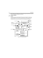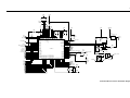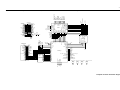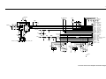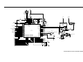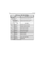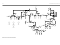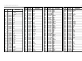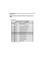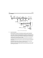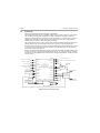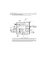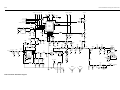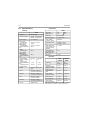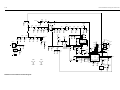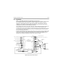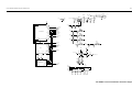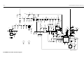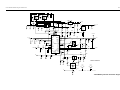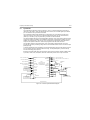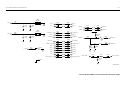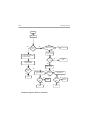
1
GP328/GP338 Portable Radios Detailed Service Manual 6804110J64-F June, 2002 Computer Software Copyrights The Motorola products described in this manual may include copyrighted Motorola computer programs stored in semiconductor memories or other media. Laws in the United States and other countries preserve for Motorola certain exclusive rights for copyrighted computer programs, including the exclusive right to copy or reproduce in any form, the copyrighted computer program. Accordingly, any copyrighted Motorola computer programs contained in the Motorola products described in this manual may not be copied or reproduced in any manner without the express written permission of Motorola. Furthermore, the purchase of Motorola products shall not be deemed to grant, either directly or by implication, estoppel or otherwise, any license under the copyrights, patents or patent applications of Motorola, except for the normal non-exclusive royalty-free license to use that arises by operation of law in the sale of a product. 1999, 2000, 2001, 2002 by Motorola, Inc. Motorola Technology Sdn. Bhd. (Co. No. 455657-H) Bayan Lepas FIZ Phase III 11900 Penang, Malaysia Printed in Malaysia June, 2002 i SAFETY AND GENERAL INFORMATION Information and Instructions on RF Energy Exposure and Product Safety READ THIS IMPORTANT INFORMATION ON SAFE AND EFFICIENT OPERATION BEFORE USING YOUR MOTOROLA HANDHELD PORTABLE TWO-WAY RADIO The information provided in this document supersedes the general safety information contained in user guides published prior to June 2001. For information regarding radio use in a hazardous atmosphere please refer to the Factory Mutual (FM) Approval Product Listing Manual or Instruction Card, which is included with radio models that offer this capability. Compliance with RF Energy Exposure Standards Your Motorola two-way radio is designed and tested to comply with a number of national and international standards and guidelines (listed below) regarding human exposure to radio frequency electromagnetic energy. This radio complies with the IEEE (FCC) and ICNIRP exposure limits for occupational/controlled RF exposure environment at duty cycles of up to 50% talk-50% listen and should be used for occupational use only. In terms of measuring RF energy for compliance with the FCC exposure guidelines, your radio radiates measurable RF energy only while it is transmitting (during talking), not when it is receiving (listening) or in standby mode. Note that the approved, supplied batteries for this radio are rated for a 5-5-90 duty cycle (5% talk - 5% listen - 90% standby), even though this radio complies with the FCC occupational exposure limits at duty cycles of up to 50% talk. Your Motorola two-way radio complies with the following RF energy exposure standards and guidelines: • • • • • • • United States Federal Communications Commission, Code of Federal Regulations; 47CFR part 2 sub-part J American National Standards Institute (ANSI) / Institute of Electrical and Electronic Engineers (IEEE) C95. 1-1992 Institute of Electrical and Electronic Engineers (IEEE) C95.1-1999 Edition International Commission on Non-Ionizing Radiation Protection (ICNIRP) 1998 Ministry of Health (Canada) Safety Code 6. Limits of Human Exposure to Radio frequency Electromagnetic Fields in the Frequency Range from 3 kHz to 300 GHz, 1999 Australian Communications Authority Radiocommunications (Electromagnetic Radiation Human Exposure) Standard 2001 ANATEL, Brazil Regulatory Authority, Resolution 256 (April 11, 2001) “additional requirements for SMR, cellular and PCS product certification.” Operational Instructions and Training Guidelines To ensure optimal performance and compliance with the occupational/controlled environment RF energy exposure limits in the above standards and guidelines, users should transmit no more than 50% of the time and always adhere to the following procedures: Transmit and Receive To transmit (talk), push the Push-To-Talk (PTT) button; to receive, release the PTT button. Hand-held Radio Operation Hold the radio in a vertical position with the microphone one to two inches (2.5 to 5 cm) away from the lips. 2.5 to 5.0 cm (1 to 2 in.) Body-worn Operation Always place the radio in a Motorola approved clip, holder, holster, case, or body harness for this product. Use of non-Motorola-approved accessories may exceed FCC RF exposure guidelines. If you do not use a Motorola approved body-worn accessory and are not using the radio in the intended use position in front of the face, then ensure the antenna and the radio are kept 2.5 cm (one inch) from the body when transmitting. ii Antennas & Batteries Use only Motorola approved supplied antenna or Motorola approved replacement antenna. Unauthorized antennas, modifications, or attachments could damage the radio and may violate FCC regulations. Use only Motorola approved supplied batteries or Motorola approved replacement batteries. Use of non-Motorola-approved antennas or batteries may exceed FCC RF exposure guidelines. Approved Accessories For a list of approved Motorola accessories please contact your dealer, or local Motorola representative. ELECTROMAGNETIC INTERFERENCE/COMPATIBILITY NOTE Nearly every electronic device is susceptible to electromagnetic interference (EMI) if inadequately shielded, designed, or otherwise configured for electromagnetic compatibility. Facilities To avoid electromagnetic interference and/or compatibility conflicts, turn off your radio in any facility where posted notices instruct you to do so. Hospitals or health care facilities may be using equipment that is sensitive to external RF energy. Aircraft When instructed to do so, turn off your radio when on board an aircraft. Any use of a radio must be in accordance with applicable regulations per airline crew instructions. Medical Devices • Pacemakers The Advanced Medical Technology Association (AdvaMed) recommends that a minimum separation of 6 inches (15 centimeters) be maintained between a handheld wireless radio and a pacemaker. These recommendations are consistent with those of the U.S. Food and Drug Administration. Persons with pacemakers should: • • • • • ALWAYS keep the radio more than 6 inches (15 centimeters) from their pacemaker when the radio is turned ON. not carry the radio in the breast pocket. use the ear opposite the pacemaker to minimize the potential for interference. turn the radio OFF immediately if you have any reason to suspect that interference is taking place. Hearing Aids Some digital wireless radios may interfere with some hearing aids. In the event of such interference, you may want to consult your hearing aid manufacturer to discuss alternatives. • Other Medical Devices If you use any other personal medical device, consult the manufacturer of your device to determine if it is adequately shielded from RF energy. Your physician may be able to assist you in obtaining this information. Driver Safety Check the laws and regulations on the use of radios in the area where you drive. Always obey them. When using your radio while driving, please: • • • Give full attention to driving and to the road. Use hands-free operation, if available. Pull off the road and park before making or answering a call if driving conditions so require. iii OPERATIONAL WARNINGS For Vehicles With an Air Bag Do not place a portable radio in the area over an air bag or in the air bag deployment area. Air bags inflate with great force. If a portable radio is placed in the air bag deployment area and the air bag inflates, the radio may be propelled with great force and cause serious injury to occupants of the vehicle. ! WARNING Potentially Explosive Atmospheres Turn off your radio prior to entering any area with a potentially explosive atmosphere, unless it is a radio type especially qualified for use in such areas as “Intrinsically Safe” (for example, Factory Mutual, CSA, UL, or CENELEC). Do not remove, install, or charge batteries in such areas. Sparks in a potentially explosive atmosphere can cause an explosion or fire resulting in bodily injury or even death. NOTE The areas with potentially explosive atmospheres referred to above include fueling areas such as below decks on boats, fuel or chemical transfer or storage facilities, and areas where the air contains chemicals or particles, such as grain, dust or metal powders. Areas with potentially explosive atmospheres are often but not always posted. Blasting Caps and Areas To avoid possible interference with blasting operations, turn off your radio when you are near electrical blasting caps, in a blasting area, or in areas posted: “Turn off two-way radio.” Obey all signs and instructions. OPERATIONAL CAUTIONS Antennas Do not use any portable radio that has a damaged antenna. If a damaged antenna comes into contact with your skin, a minor burn can result. ! Caution Batteries All batteries can cause property damage and/or bodily injury such as burns if a conductive material such as jewelry, keys, or beaded chains touch exposed terminals. The conductive material may complete an electrical circuit (short circuit) and become quite hot. Exercise care in handling any charged battery, particularly when placing it inside a pocket, purse, or other container with metal objects. iv v Table of Contents Section 1 Introduction 1.0 Scope of Manual.................................................................................................. 1-1 2.0 Warranty and Service Support............................................................................. 1-1 2.1 Warranty Period ............................................................................................. 1-1 2.2 After Warranty Period..................................................................................... 1-1 2.3 Piece Parts ..................................................................................................... 1-2 2.4 Technical Support .......................................................................................... 1-2 Section 2 Service Aids 1.0 Recommended Test Tools................................................................................... 2-1 Section 3 Power Up Self-Test 1.0 Error Codes ......................................................................................................... 3-1 Section 4 Controller Information 1.0 Overview.............................................................................................................. 4-1 2.0 Radio Power Distribution ..................................................................................... 4-1 3.0 Controller Board................................................................................................... 4-2 3.1 General........................................................................................................... 4-2 3.2 Digital Architecture ......................................................................................... 4-3 3.3 Controller Schematics (330-400MHz for 8485726Z01, 403-470MHz for 8480450Z03 & 450-527MHz for 8485641Z02)............................................... 4-5 Complete Controller Schematic Diagram ............................................................... 4-5 Controller ASFIC/ON_OFF Schematic Diagram .................................................... 4-6 Controller Micro Processor Schematic Diagram .................................................... 4-7 Controller Memory Schematic Diagram ................................................................. 4-8 Controller Audio Power Amplifier Schematic Diagram ........................................... 4-9 Controller Interface Schematic Diagram .............................................................. 4-10 3.4 Controller Schematics (330-400MHz for 8485726Z04, 403-470MHz for 8480450Z13 & 450-527MHz for 8485641Z06)............................................. 4-11 Complete Controller Schematic Diagram ............................................................. 4-11 Controller ASFIC/ON_OFF Schematic Diagram .................................................. 4-12 Controller Micro Processor Schematic Diagram .................................................. 4-13 Controller Memory Schematic Diagram ............................................................... 4-14 Controller Audio Power Amplifier Schematic Diagram ......................................... 4-15 Controller Interface Schematic Diagram .............................................................. 4-16 3.5 Controller Schematics (136-174MHz for 8486062B09 & 8486062B12)....... 4-17 Complete Controller Schematic Diagram ............................................................. 4-17 vi Controller ASFIC/ON_OFF Schematic Diagram...................................................4-18 Controller Micro Processor Schematic Diagram ...................................................4-19 Controller Memory Schematic Diagram ................................................................4-20 Controller Audio Power Amplifier Schematic Diagram..........................................4-21 Controller Interface Schematic Diagram ...............................................................4-22 3.6 Controller Schematics (136-174MHz) for PCB 8486062B16........................4-23 Complete Controller Schematic Diagram..............................................................4-23 Controller ASFIC/ON_OFF Schematic Diagram...................................................4-24 Controller Micro Processor Schematic Diagram ...................................................4-25 Controller Memory Schematic Diagram ................................................................4-26 Controller Audio Power Amplifier Schematic Diagram..........................................4-27 Controller Interface Schematic Diagram ...............................................................4-28 3.7 Controller Schematics (29-42/35-50MHz) ....................................................4-29 Controller Hierarchical Diagram............................................................................4-29 Complete Controller Schematic Diagram..............................................................4-30 Controller ASFIC/ON_OFF Schematic Diagram...................................................4-31 Controller Microprocessor Schematic Diagram ...................................................4-32 Controller Interface and Memory Schematic Diagram ..........................................4-33 Controller Audio Power Amplifier Schematic Diagram..........................................4-34 Section 5 1.0 2.0 3.0 4.0 Keypad Board Information Theory of Operation .............................................................................................5-1 Troubleshooting Chart..........................................................................................5-2 Parts List (Keypad Basic).....................................................................................5-3 Keypad Board And Schematic Diagram...............................................................5-5 Keypad Board Top and Bottom View (PCB No. 8480574Z05) ...............................5-5 Keypad Board Schematic Diagram.........................................................................5-6 Section 6A Model Chart and Test Specifications (403-470 Mhz) 1.0 Model Chart....................................................................................................... 6A-1 2.0 Specifications .................................................................................................... 6A-3 3.0 Transmitter ........................................................................................................ 6A-4 3.1 General ........................................................................................................ 6A-4 4.0 Receiver ............................................................................................................ 6A-6 4.1 Receiver Front-End...................................................................................... 6A-6 4.2 Receiver Back-End ...................................................................................... 6A-7 4.3 Automatic Gain Control Circuit .................................................................... 6A-8 5.0 Frequency Generation Circuitry ........................................................................ 6A-9 5.1 Synthesizer ................................................................................................ 6A-10 5.2 VCO - Voltage Controlled Oscillator .......................................................... 6A-11 6.0 Notes For All Schematics and Circuit Boards ................................................. 6A-13 7.0 Circuit Board/Schematic Diagrams and Parts List .......................................... 6A-15 UHF (403-470MHz) Main Board Top Side PCB No. 8480450Z03..................... 6A-15 UHF (403-470MHz) Main Board Bottom Side PCB No. 8480450Z03 ............... 6A-16 vii UHF Controls And Switches Schematic Diagram ..............................................6A-17 UHF Receiver Front End Schematic Diagram....................................................6A-18 UHF Receiver Back End Schematic Diagram ....................................................6A-19 UHF Synthesizer Schematic Diagram ................................................................6A-20 UHF Voltage Controlled Oscillator Schematic Diagram .....................................6A-21 UHF Transmitter Schematic Diagram ................................................................6A-22 UHF Radio Parts List..........................................................................................6A-23 8.0 Circuit Board/Schematic Diagrams and Parts List...........................................6A-26 UHF (403-470MHz) Main Board Top Side PCB No. 8480450Z13 .....................6A-26 UHF (403-470MHz) Main Board Bottom Side PCB No. 8480450Z13 ................6A-27 UHF Controls And Switches Schematic Diagram ..............................................6A-28 UHF Receiver Front End Schematic Diagram....................................................6A-29 UHF Receiver Back End Schematic Diagram ....................................................6A-30 UHF Synthesizer Schematic Diagram ................................................................6A-31 UHF Voltage Controlled Oscillator Schematic Diagram .....................................6A-32 UHF Harmonic Filter Schematic Diagram ..........................................................6A-33 UHF Transmitter Schematic Diagram ................................................................6A-34 UHF Radio Parts List..........................................................................................6A-35 9.0 Troubleshooting charts ....................................................................................6A-39 Troubleshooting Flow Chart for Controller .........................................................6A-39 Troubleshooting Flow Chart for Receiver (Sheet 1 of 2) ....................................6A-40 Troubleshooting Flow Chart for Receiver (Sheet 2 of 2) ....................................6A-41 Troubleshooting Flow Chart for Transmitter .......................................................6A-42 Troubleshooting Flow Chart for Synthesizer ......................................................6A-43 Troubleshooting Flow Chart for VCO .................................................................6A-44 Section 6B Model Chart and Test Specifications (136-174 Mhz) 1.0 Model Chart .......................................................................................................6B-1 2.0 Specifications.....................................................................................................6B-3 3.0 Transmitter.........................................................................................................6B-4 3.1 General.........................................................................................................6B-4 4.0 Receiver.............................................................................................................6B-6 4.1 Receiver Front-End ......................................................................................6B-6 4.2 Receiver Back-End.......................................................................................6B-7 4.3 Automatic Gain Control Circuit .....................................................................6B-8 5.0 Frequency Generation Circuitry.........................................................................6B-9 5.1 Synthesizer.................................................................................................6B-10 5.2 VCO - Voltage Controlled Oscillator...........................................................6B-11 6.0 Notes For All Schematics and Circuit Boards..................................................6B-13 7.0 Circuit Board/Schematic Diagrams and Parts List...........................................6B-15 VHF (136-174MHz) Main Board Top Side PCB No. 8486062B09 .....................6B-15 VHF (136-174MHz) Main Board Bottom Side PCB No. 8486062B09 ................6B-16 VHF (136-174MHz) Main Board Top Side PCB No. 8486062B12 .....................6B-17 VHF (136-174MHz) Main Board Bottom Side PCB No. 8486062B12 ................6B-18 VHF Controls And Switches Schematic Diagram...............................................6B-19 viii VHF Receiver Front End Schematic Diagram ................................................... 6B-20 VHF Receiver Back End Schematic Diagram.................................................... 6B-21 VHF Synthesizer Schematic Diagram................................................................ 6B-22 VHF Voltage Controlled Oscillator Schematic Diagram..................................... 6B-23 VHF Transmitter Schematic Diagram ................................................................ 6B-24 VHF Radio Parts List ......................................................................................... 6B-25 8.0 Circuit Board/Schematic Diagrams and Parts List .......................................... 6B-29 VHF (136-174MHz) Main Board Top Side PCB No. 8486062B16..................... 6B-29 VHF (136-174MHz) Main Board Bottom Side PCB No. 8486062B16 ............... 6B-30 VHF Controls And Switches Schematic Diagram .............................................. 6B-31 VHF Receiver Front End Schematic Diagram ................................................... 6B-32 VHF Receiver Back End Schematic Diagram.................................................... 6B-33 VHF Synthesizer Schematic Diagram................................................................ 6B-34 VHF Voltage Controlled Oscillator Schematic Diagram..................................... 6B-35 VHF Transmitter Schematic Diagram ................................................................ 6B-36 VHF Radio Parts List ......................................................................................... 6B-37 9.0 Troubleshooting charts.................................................................................... 6B-41 Troubleshooting Flow Chart for Controller ......................................................... 6B-41 Troubleshooting Flow Chart for Receiver (Sheet 1 of 2).................................... 6B-42 Troubleshooting Flow Chart for Receiver (Sheet 2 of 2).................................... 6B-43 Troubleshooting Flow Chart for Transmitter ...................................................... 6B-44 Troubleshooting Flow Chart for Synthesizer...................................................... 6B-45 Troubleshooting Flow Chart for VCO................................................................. 6B-46 Section 6C Model Chart and Test Specifications (450-527 Mhz) 1.0 Model Chart....................................................................................................... 6C-1 2.0 Specifications .................................................................................................... 6C-2 3.0 Transmitter ........................................................................................................ 6C-3 3.1 General ........................................................................................................ 6C-3 4.0 Receiver ............................................................................................................ 6C-5 4.1 Receiver Front-End...................................................................................... 6C-5 4.2 Receiver Back-End ...................................................................................... 6C-6 4.3 Automatic Gain Control Circuit .................................................................... 6C-7 5.0 Frequency Generation Circuitry ........................................................................ 6C-8 5.1 Synthesizer .................................................................................................. 6C-9 5.2 VCO - Voltage Controlled Oscillator .......................................................... 6C-10 6.0 Notes For All Schematics and Circuit Boards ................................................. 6C-12 7.0 Circuit Board/Schematic Diagrams and Parts List .......................................... 6C-13 UHF Band 2 (450-527MHz) Main Board Top Side PCB No. 8485641Z02 ........ 6C-13 UHF Band 2 (450-527MHz) Main Board Bottom Side PCB No. 8485641Z02 ... 6C-14 UHF Band 2 Controls And Switches Schematic Diagram.................................. 6C-15 UHF Band 2 Receiver Front End Schematic Diagram....................................... 6C-16 UHF Band 2 Receiver Back End Schematic Diagram ....................................... 6C-17 UHF Band 2 Synthesizer Schematic Diagram ................................................... 6C-18 UHF Band 2 Voltage Controlled Oscillator Schematic Diagram ........................ 6C-19 ix UHF Band 2 Transmitter Schematic Diagram ................................................... 6C-20 UHF Band 2 Radio Parts List ............................................................................ 6C-21 8.0 Circuit Board/Schematic Diagrams and Parts List.......................................... 6C-25 UHF Band 2 (450-527MHz) Main Board Top Side PCB No. 8485641Z06........ 6C-25 UHF Band 2 (450-527MHz) Main Board Bottom Side PCB No. 8485641Z06 .. 6C-26 UHF Band 2 Controls And Switches Schematic Diagram ................................. 6C-27 UHF Band 2 Receiver Front End Schematic Diagram ...................................... 6C-28 UHF Band 2 Receiver Back End Schematic Diagram....................................... 6C-29 UHF Band 2 Synthesizer Schematic Diagram .................................................. 6C-30 UHF Band 2 Voltage Controlled Oscillator Schematic Diagram........................ 6C-31 UHF Band 2 Transmitter Schematic Diagram ................................................... 6C-32 UHF Band 2 Radio Parts List ............................................................................ 6C-33 9.0 Troubleshooting charts ................................................................................... 6C-37 Troubleshooting Flow Chart for Controller ........................................................ 6C-37 Troubleshooting Flow Chart for Receiver (Sheet 1 of 2) ................................... 6C-38 Troubleshooting Flow Chart for Receiver (Sheet 2 of 2) ................................... 6C-39 Troubleshooting Flow Chart for Transmitter ...................................................... 6C-40 Troubleshooting Flow Chart for Synthesizer ..................................................... 6C-41 Troubleshooting Flow Chart for VCO ................................................................ 6C-42 Section 6D Model Chart and Test Specifications (330-400 Mhz) 1.0 Model Chart ...................................................................................................... 6D-1 2.0 Specifications.................................................................................................... 6D-2 3.0 Transmitter........................................................................................................ 6D-3 3.1 General........................................................................................................ 6D-3 4.0 Receiver............................................................................................................ 6D-5 4.1 Receiver Front-End ..................................................................................... 6D-5 4.2 Receiver Back-End...................................................................................... 6D-6 4.3 Automatic Gain Control Circuit .................................................................... 6D-7 5.0 Frequency Generation Circuitry........................................................................ 6D-8 5.1 Synthesizer.................................................................................................. 6D-9 5.2 VCO - Voltage Controlled Oscillator.......................................................... 6D-10 6.0 Notes For All Schematics and Circuit Boards................................................. 6D-12 7.0 Circuit Board/Schematic Diagrams and Parts List.......................................... 6D-13 330-400MHz Main Board Top Side PCB No. 8485726Z01 ............................... 6D-13 330-400MHz Main Board Bottom Side PCB No. 8485726Z01.......................... 6D-14 330-400MHz Controls And Switches Schematic Diagram ................................ 6D-15 330-400MHz Receiver Front End Schematic Diagram ..................................... 6D-16 330-400MHz Receiver Back End Schematic Diagram...................................... 6D-17 330-400MHz Synthesizer Schematic Diagram.................................................. 6D-18 330-400MHz Voltage Controlled Oscillator Schematic Diagram ....................... 6D-19 330-400MHz Transmitter Schematic Diagram .................................................. 6D-20 330-400MHz Radio Parts List ........................................................................... 6D-21 x 8.0 Circuit Board/Schematic Diagrams and Parts List .......................................... 6D-24 330-400MHz Main Board Top Side PCB No. 8485726Z04 ............................... 6D-24 330-400MHz Main Board Bottom Side PCB No. 8485726Z04 .......................... 6D-25 330-400MHz Controls And Switches Schematic Diagram................................. 6D-26 330-400MHz Receiver Front End Schematic Diagram ...................................... 6D-27 330-400MHz Receiver Back End Schematic Diagram ...................................... 6D-28 330-400MHz Synthesizer Schematic Diagram .................................................. 6D-29 330-400MHz Voltage Controlled Oscillator Schematic Diagram ....................... 6D-30 330-400MHz Transmitter Schematic Diagram................................................... 6D-31 330-400MHz Radio Parts List ............................................................................ 6D-32 9.0 Troubleshooting charts.................................................................................... 6D-37 Troubleshooting Flow Chart for Controller ......................................................... 6D-37 Troubleshooting Flow Chart for Receiver (Sheet 1 of 2).................................... 6D-38 Troubleshooting Flow Chart for Receiver (Sheet 2 of 2).................................... 6D-39 Troubleshooting Flow Chart for Transmitter ...................................................... 6D-40 Troubleshooting Flow Chart for Synthesizer...................................................... 6D-41 Troubleshooting Flow Chart for VCO................................................................. 6D-42 Section 6E Model Charts and Test Specifications (29-42/35-50Mhz) 1.0 Model Charts..................................................................................................... 6E-1 1.1 29-42MHz .................................................................................................... 6E-1 1.2 35-50MHz .................................................................................................... 6E-2 2.0 Specifications .................................................................................................... 6E-3 3.0 Transmitter ........................................................................................................ 6E-4 3.1 General ........................................................................................................ 6E-4 4.0 Receiver ............................................................................................................ 6E-6 4.1 Receiver Front-End...................................................................................... 6E-6 4.2 Receiver Back-End ...................................................................................... 6E-7 4.3 Automatic Gain Control Circuit .................................................................... 6E-7 5.0 Frequency Generation Circuitry ........................................................................ 6E-8 5.1 Synthesizer .................................................................................................. 6E-9 5.2 VCO - Voltage Controlled Oscillator .......................................................... 6E-10 6.0 Notes For All Schematics and Circuit Boards ................................................. 6E-11 7.0 Circuit Board/Schematic Diagrams and Parts List .......................................... 6E-13 Lowband 29-42/35-50MHz Main Board Top Side PCB No. 8486291A02 ......... 6E-13 Lowband 29-42/35-50MHz Main Board Bottom Side PCB No. 8486291A02 ... 6E-14 Lowband 29-42/35-50MHz Controls And Switches Schematic Diagram ........... 6E-15 Lowband 29-42/35-50MHz Overall Receiver Schematic Diagram..................... 6E-16 Lowband 29-42/35-50MHz Receiver Front End Schematic Diagram ................ 6E-17 Lowband 29-42/35-50MHz Receiver Back End Schematic Diagram................. 6E-18 Lowband 29-42/35-50MHz Synthesizer Schematic Diagram ............................ 6E-19 Lowband 29-42/35-50MHz Voltage Controlled Oscillator Schematic Diagram.. 6E-20 Lowband 29-42/35-50MHz Transmitter Schematic Diagram ............................. 6E-21 Lowband 29-42/35-50MHz Radio Parts List ...................................................... 6E-22 xi 8.0 Troubleshooting charts ....................................................................................6E-25 Troubleshooting Flow Chart for Controller .........................................................6E-25 Troubleshooting Flow Chart for Receiver (Sheet 1 of 2) ....................................6E-26 Troubleshooting Flow Chart for Receiver (Sheet 2 of 2) ....................................6E-27 Troubleshooting Flow Chart for Transmitter .......................................................6E-28 Troubleshooting Flow Chart for Synthesizer ......................................................6E-29 Troubleshooting Flow Chart for VCO .................................................................6E-30 Section 7 1.0 2.0 3.0 4.0 5.0 6.0 Flex Layout/Schematic Diagrams and Parts Lists Keypad-Controller Interconnect Flex ................................................................... 7-1 Schematic for Keypad-Controller Interconnect Flex ............................................ 7-1 Parts List for Keypad-Controller Interconnect Flex .............................................. 7-2 Universal Connector Flex .................................................................................... 7-2 Schematic for Universal Connector Flex ............................................................. 7-3 Parts List for Universal Connector Flex ............................................................... 7-3 xii 1-1 Section 1 INTRODUCTION 1.0 Scope of Manual This manual is intended for use by service technicians familiar with similar types of equipment. It contains service information required for the equipment described and is current as of the printing date. Changes which occur after the printing date may be incorporated by a complete Manual revision or alternatively as additions. NOTE Before operating or testing these units, please read the Safety Information Section in the front of this manual. 2.0 Warranty and Service Support Motorola offers long term support for its products. This support includes full exchange and/or repair of the product during the warranty period, and service/repair or spare parts support out of warranty. Any "return for exchange" or "return for repair" by an authorised Motorola Dealer must be accompanied by a Warranty Claim Form. Warranty Claim Forms are obtained by contacting an Authorised Motorola Dealer. 2.1 Warranty Period The terms and conditions of warranty are defined fully in the Motorola Dealer or Distributor or Reseller contract. These conditions may change from time to time and the following notes are for guidance purposes only. In instances where the product is covered under a "return for replacement" or "return for repair" warranty, a check of the product should be performed prior to shipping the unit back to Motorola. This is to ensure that the product has been correctly programmed or has not been subjected to damage outside the terms of the warranty. Prior to shipping any radio back to the appropriate Motorola warranty depot, please contact Customer Services. All returns must be accompanied by a Warranty Claim Form, available from your Customer Services representative. Products should be shipped back in the original packaging, or correctly packaged to ensure no damage occurs in transit. 2.2 After Warranty Period After the Warranty period, Motorola continues to support its products in two ways. 1. Motorola's Accessories and Aftermarket Division (AAD) offers a repair service to both end users and dealers at competitive prices. 2. AAD supplies individual parts and modules that can be purchased by dealers who are technically capable of performing fault analysis and repair. 1-2 2.3 Warranty and Service Support Piece Parts Some replacement parts, spare parts, and/or product information can be ordered directly. If a complete Motorola part number is assigned to the part, it is available from Motorola’s Accessories and Aftermarket Division (AAD). If no part number is assigned, the part is not normally available from Motorola. If the part number is appended with an asterisk, the part is serviceable by Motorola Depot only. If a parts list is not included, this generally means that no user-serviceable parts are available for that kit or assembly. All orders for parts/information should include the complete Motorola identification number. All part orders should be directed to your local AAD office. Please refer to your latest price pages. 2.4 Technical Support Technical support is available to assist the dealer/distributor in resolving any malfunction which may be encountered. Initial contact should be by telephone wherever possible. When contacting Motorola Technical Support, be prepared to provide the product model number and the unit’s serial number. Toll-Free Country or Territory Number China 800-810-0976 Indonesia 0800-1-686868 Malaysia 1800-801687 Philippines 1800-16510271 Singapore 1800-4855333 Thailand 1800-225412 Non-Toll-Free Country or Territory Number China (86-10) 6843-8231 Hong Kong SAR (852) 2966-4188 India (91) 80-658-7677-7678 Indonesia (62-21) 251-3050 Korea (822) 3466-5401 Malaysia (603) 7803-9922 Philippines (63-2) 810-0762 Singapore (65) 486-7171 Taiwan (886) 2-27058000 ext. 6308 Thailand (66) 2254-8388 Vietnam (84) 8-8294091 All Other Countries IDD code + (65) 4855333 2-1 Section 2 SERVICE AIDS 1.0 Recommended Test Tools Table 2-1 lists the tools recommended for working on this family of radios. These tools are also available from Motorola. Table 2-1: Recommended Test Tools Motorola Part No. 6680387A59 6680387A64 6680387A65 0180382A31 6680375A74 0180386A81 0180386A78 0180386A82 6684253C72 6680384A98 1010041A86 1080370B43 R-1070A or R-1319A Description Application Extractor, 2-contact Heat controller with safety stand or Safety stand only Portable desoldering unit Removal of discrete surface-mounted devices 0.025 replacement tip, 5/pk Miniature digital readout soldering station (incl. 1/64” micropoint tip) Illuminated magnifying glass with lens attachment. For 0180382A31 portable desoldering unit. Anti-static grounding kit Straight prober Brush Solder (RMA type), 63/37, 0.020” diameter 1 lb. spool RMA liquid flux Used during all radio assembly and disassembly procedures Shields and surfacemounted component - IC removal/rework station (order all heat-focus heads separately) Shields and surfacemounted component - IC removal/rework station SMD10000 M.A.P.E. Removal and assembly of surface-mounted integrated circuits and shields Removal and assembly of surface-mounted integrated circuits and shields 2-2 Recommended Test Tools 3-1 Section 3 POWER UP SELF-TEST 1.0 Error Codes Turning on the radio using the on/off volume control starts a self-test routine which checks the RAM, ROM checksum, EEPROM hardware and EEPROM checksum. If these checks are successfully completed, the radio will generate the Self-Test Pass Tone. If the self-test is not successful, a “bonk” is heard. Radios with displays are able to display these error messages: • • • • “RAM TST ERROR” for <RAM Test Error> “ROM CS ERROR” for <ROM Checksum Error> “EEPRM HW ERROR” for <EEPROM Hardware Test Error> “EEPRM CS ERROR” for <EEPROM Checksum Error> NOTE Radio without display emits only “bonk” (300 Hz) tone if it fails the self-test. Error Code Explanation Corrective Action “RAM TST ERROR” RAM Test Failure Retest radio by turning it off and turning it on again. If message reoccurs, replace RAM (U405). “ROM CS ERROR” ROM Checksum is wrong. Reprogram FLASH Memory, then retest. If message reoccurs, replace ROM (U406). “EEPRM HW ERROR” Codeplug structure mismatch, non existence of codeplug. Reprogram codeplug with correct version and retest radio. If message reoccurs, replace EEPROM (U407). “EEPRM CS ERROR” Codeplug checksum is wrong. Reprogram codeplug. No Display Display module is not connected properly. Display module is damaged. Check connection between main board and display module. Replace with new display module. 3-2 Error Codes 4-1 Section 4 CONTROLLER INFORMATION 1.0 Overview This section provides a detailed theory of operation for the radio and its components. 2.0 Radio Power Distribution Accessories 20 pin Connector Keypad/Option Board Audio PA Int/Ext Vdd Prime Expansion Board Switching Reg. R4 4.0V/3.3V 7.5V Battery Vdda Vdda Reg. UNSWB+ Fuse SWB+ R5 R2 R1 Vddd Reg. R3 Vddd TX. Led MECH. SWB+ 3.5V Reg. MCU Micro P, ROM & EEPROM Control LCD Driver ASFIC_CMP FRACTN VCOBIC LVZIF On/Off Switch LI Ion 5V Reg. Low Battery Detect 5V Jumpers Ant. SW PA, Driver PCIC(ALC) RF. AMP, IF AMP Ext. RX. Buffer (NU) Dual Vdd Regulator Scheme Single Vdd Regulator Scheme R1 Y Y R2 N N R3 N Y R4 N N R5 Y N Vdda Y N SW. Reg. N N Figure 4-1: DC Power Distribution Block Diagram Figure 4-1 illustrates the DC distribution throughout the radio board. A 7.5V battery (BATT 7.5V) supplies power directly to the electronic on/off control as UNSWB+. When the radio is turned on, MECH_SWB+ (on/off/volume control) will trigger the electronic on/off control(momentary-on path), then SWB+ is distributed as shown in Figure 4-1. Vdda from 3.3V Vdda regulator will then supply the microprocessor. Data is then sent to ASFIC_CMP to turn on GCB4(DAC). GCB4 will take over the momentary-on path within 12ms. SWB+ will continue to support the whole board until the radio is turned off. Radio will be turned-off on two conditions; 1. MECH_SWB+ turned off 2. Low battery 4-2 Controller Board When low battery level is detected by the microprocessor through both conditions above, it will store the radio personality data to EEPROM before turning off. 3.0 Controller Board 3.1 General The controller board is the central interface between the various subsytems of the radio. It is separated into digital and audio architectures. The digital portion consists of a special Motorola microcontroller (HC11FL0). The audio power amplifier (Audio PA) and audio/signalling/filter/ companding IC (ASFIC_CMP) form the backbone of the audio/signalling architecture. External Microphone To Synthesizer Mod Out Internal Microphone 16.8 MHz Reference Clock from Synthesizer Audio/Signalling Architecture Recovered Audio Squelch Audio PA ASFIC_CMP Internal Speaker 3.3V Regulator (Vdda) µP Clock SPI To RF Board Digital Architecture RAM 3.3V Regulator (Vddd) External Speaker EEPROM HC11FL0 ROM Figure 4-2: Controller Block Diagram SCI to Side Connector Controller Board Digital Architecture MCU configuration There is one common MCU architecture for low-tier as well as for the high-tier products. It covers the Conventional and Trunking portables. An open architecture system with the new HC11FL0 as the processor is used. Combinations of different size RAM, ROM and EEPROM are available for various application software. REAL TIME CLOCK (RTC) This radio supports Real Time Clock (RTC) module for purposes of Message Time Stamping and Time Keeping. The RTC module resides in the micro-processor HC11FL0. It is kept alive by a backup Lithium Ion battery when the primary battery is removed. UNSWB+ Vddd U410 R461 C435 VIN VOUT 3.3V 3 1 VSS 2 R460 C434 HC11FL0 MODA MODB 1 CR411 5 Q416 4 2 3 PI6 R420 FL401 38.4kHz OUT R419 3 C436 LI_ION 1 R462 GND R426 2 IN R463 300 PI7 C437 5 CR413 1 4 Q417 3 1 BOOT_CTRL 2 6 1 3.2 4-3 2 UNSWB+ 3 4 SWB+ TP405 TEST_POINT Figure 4-3: RTC Circuit Circuit Description The RTC module which resides in the HC11FL0 is powered by the ModB/Vstby pin and PI6/PI7 form the crystal oscillator circuit. Clock frequency of 38.4kHz from a crystal oscillator provides the reference signal. In the processor, the frequency is divided down to 1Hz. As the RTC module is powered separately from the processor Vdd, the RTC is kept alive through the ModB / Vstby pin when the radio is switched off. A small button Lithium Ion battery continues to feed the RTC when the primary battery is removed. A MOSFET Q416 switches in the LiO supply when Vdd is removed. Q416 also provides isolation from BOOT_CTRL function in the event of radio program flashing. A small 3.3V regulator is used to charge the LiO battery. 4-4 Controller Board ModB/Vstby Supply Under various conditions, the supply to the ModB/Vstby would vary. Table 4-1 shows these conditions and circuits in operation. Table 4-1: ModB/Vstby Supply Modes Condition Circuit Operation Radio On Vdd supply voltage via CR411 Radio Off • Vdd turned off • Q416 gate is pulled low by R462 • Q416 is switched on • U410 supplies 3.2V to ModB/Vstby Primary battery removed • Vdd turned off • Q416 gate is pulled low by R462 • Q416 is switched on • LiO battery provides 3.2V to ModB/Vstby Flash Mode • Boot_Ctrl line pull low • ModA & ModB goes low • Processor in boot-strap mode • Flashing enabled 4-5 EXT_MIC GREEN_LED FLAT_RX_SND BATT_CODE GREEN_LED LEDBL URX_SND TX_AUD_RTN MODIN EXT_MIC ASFIC FLAT_RX_SND UNSWB+ SWB+ VOX RESET 5V CHACT F1200 BATT_DATA_IN AUDIO_PA_ENA SYN DATA VS_GAINSEL MISO VS_GAINSEL EE_CS VS_AUDSEL CLK DACRX CSX DACRX VS_AUDSEL AUDIO INT_MIC EXT_SPKR_SEL HSIO Vddd DEMOD LSIO Vddd DEMOD SQ_DET 4V_3.3V Vdda UNSWB+ R403 NU SWB+ CSX MISO AUDIO INT_MIC EXT_MIC CLK C432 NU EXT_SPKR_SEL DATA AUDIO_PA_ENA RESET FLAT_RX_SND Vddd 5V Vdda Vdda 5V Vdda RESET BATT_CODE LI_ION 4V_3.3V 4V_3.3V SWB+ IF_5V_CTRL IF_Vdda_CTRL IF_RESET_CTRL IF_BATT_CODE_CTRL IF_LI_ION_CTRL IF_4V_3.3V_CTRL RED_LED GREEN_LED SB1 SB2 SB3 EMER RTA0 RTA1 RTA2 RTA3 MECH_SWB+ VOL PTT LVZIF_SEL SWB+ DACRx CSX MODIN DATA CLK LOCK UNSWB+ DEMOD RSSI 16.8MHz UNSWB+ 5V Vdda RESET BATT_CODE LI_ION 4V_3.3V IF_RED_LED_CTRL IF_GREEN_LED_CTRL IF_SB1_CTRL IF_SB2_CTRL IF_SB3_CTRL IF_EMER_CTRL IF_RTA0_CTRL IF_RTA1_CTRL IF_RTA2_CTRL IF_RTA3_CTRL IF_MECHSWB+_CTRL IF_VOL_CTRL IF_PTT_CTRL IF_LVZIF_SEL_CTRL IF_SWB+_CTRL IF_DACRX_CTRL IF_CSX_CTRL IF_MODIN_CTRL IF_DATA_CTRL IF_CLK_CTRL IF_LOCK_CTRL IF_UNSWB+_CTRL IF_DEMOD_CTRL IF_RSSI_CTRL IF_16.8MHz_CTRL OFF_BATT_DATA_OUT TO/FROM RF RED_LED GREEN_LED SB1 SB2 SB3 EMER RTA0 RTA1 RTA2 RTA3 MECH_SWB+ VOL PTT LVZIF_SEL SWB+ DACRx CSX MODIN DATA CLK LOCK UNSWB+ DEMOD RSSI 16.8MHz 5V INT_EXT_Vdd BATT_CODE Vdda MECH_SWB+ INT_EXT_Vdd LEDBL MECH_SWB+ FLAT_TX_RTN URX_SND RX_AUD_RTN FLAT_TX_RTN MODIN TX_AUD_SND RX_AUD_RTN 16.8MHz TX_AUD_SND RED_LED 16.8MHz TX_AUD_RTN RED_LED OFF_BATT_DATA_OUT Controller Schematics (330-400MHz for 8485726Z01, 403-470MHz for 8480450Z03 & 450-527MHz for 8485641Z02) RDY FLASH_OE BOOT_CTRL RAM_CS RSSI R_W RTA0 RTA0 Vddd RTA1 RTA1 D0 D1 D2 D3 D4 D5 D6 D7 RTA2 RTA2 RTA3 RTA3 SB1 SB1 SB2 SB2 SB3 SB3 OFF_BATT_DATA_OUT LI_ION OPT_ENA MECH_SWB+ VOL RSSI LI_ION OPT_ENA MECH_SWB+ VOL VS_RAC KEYPAD_COL KEYPAD_COL KEYPAD_ROW KEYPAD_ROW SH400 SHIELD LOCK 1 VS_INT BOOT_CTRL OFF_BATT_DATA_OUT LOCK VS_INT EMER VS_RAC RSSI SCI_TX SCI_RX PTT SCI_RX OPT_SEL2 FLASH_EN A0 A1 A2 A3 A4 A5 A6 A7 A8 A9 A10 A11 A12 A13 A14 A15 A16 A17 SCI_TX RDY OPT_SEL1 XA18 MICRO_P OPT_SEL2 OPT_SEL1 UNSWB+ SWB+ RESET VOX CHACT F1200 BATT_DATA_IN SYN DATA CLK CSX HSIO LSIO SQ_DET MISO EE_CS LCD_SEL PTT Vddd R_W RAM_CS VS_CS EMER CLK VS_RAC MEMORY A0 A1 A2 A3 A4 A5 A6 A7 A8 A9 A10 A11 A12 A13 A14 A15 A16 A17 LCD_SEL LVZIF_SEL KEY_INT D0 D1 D2 D3 D4 D5 D6 D7 FLASH_OE INT_EXT_Vdd KEYPAD_ROW KEYPAD_COL PTT KEY_INT VS_INT RESET LEDBL OFF_BATT_DATA_OUT VS_GAINSEL MISO DATA R_W LCD_SEL VS_CS KEY_INT Vddd R_W RAM_CS LVZIF_SEL EXT_MIC VS_CS SWB+ Vddd VS_AUDSEL FLAT_RX_SND RX_AUD_RTN TX_AUD_SND TX_AUD_RTN FLAT_TX_RTN OPT_ENA RDY URX_SND XA18 EXT_MIC VS_CS SWB+ Vddd VS_AUDSEL FLAT_RX_SND RX_AUD_RTN TX_AUD_SND TX_AUD_RTN FLAT_TX_RTN OPT_ENA RDY URX_SND ON INT_EXT_Vdd KEYPAD_ROW KEYPAD_COL PTT KEY_INT VS_INT RESET LEDBL OFF_BATT_DATA_OUT VS_GAINSEL MISO DATA R_W LCD_SEL D0 D1 D2 D3 D4 D5 D6 D7 A0 CLK VS_RAC FLASH_OE INTERFACE FLASH_EN XA18 AUDIO_PA FLASH_EN 3.3 MEMORY SHIELD SH401 SHIELD 1 ON/OFF SHIELD SH402 SHIELD 1 MICROPIC SHIELD SH403 SHIELD 1 ASFIC/AUDIO PA SHIELD Complete Controller Schematic Diagram 4-6 4V_3.3V R405 0 R402 NU SWB+ Vddd 3 C401 0.1uF R401 0 C409 0.1uF CR412 2 4 Q405 3 4 1 4 1 R407 68K C403 10uF 1 5 2 6 R427 2.7K R406 75K GND C408 100pF INPUT OUTPUT FEEDBACK ERROR SHUTDOWN SENSE VTAP Vddd UNSWB+ 1 C402 0.1uF U400 LP2951ACMM-3.3 8 7 3 BATT_CODE 2 C400 .01uF INT_EXT_Vdd TP410 Q400 1 INT_MIC EXT_MIC TP406 5 Vdda C407 0.1uF 1 RESET C410 0.1uF R475 0 DEMOD LEDBL R445 24K C480 10uF 2 3 1 3 Q403 1 2 R446 220K C430 0.1uF FLAT_RX_SND C414 0.1uF C415 .01uF C452 4.7uF C451 .022uF VDDA DISC GNDA DACU DACR DACG VOX PLCAP SQIN UIO VDDDAC AGCCAP U404 09Z41 TXRTN GCB3 CLK168 VDDD VDDCP GNDD GNDD0 F1200 SYN VDDSYN NC PLCAP2 GCB2 GCB1 GCB0 CHACT SQDET LSIO HSIO CSX CLK DATA GNDSYN LCAP DACRx VS_GAINSEL VS_AUDSEL VOX 1 2 3 4 5 6 7 8 9 10 11 12 36 35 34 33 32 31 30 29 28 27 26 25 TX_AUD_RTN RED_LED 16.8MHz C419 NU F1200 SYN C416 0.1uF 13 14 15 16 17 18 19 20 21 22 23 24 R449 24K MICEXT GNDRC MICINT VDDRC TXSND AUXRX AUXTX AUDIO MOD URXOUT GCB5 GCB4 48 47 46 45 44 43 42 41 40 39 38 37 Vdda C411 0.1uF FLAT_TX_RTN AUDIO MODIN RX_AUD_RTN TX_AUD_SND C479 0.1uF R447 1.5MEG MECH_SWB+ R416 39K CR440 URX_SND R425 30K Vdda C420 .01uF C421 0.1uF R400 47K C422 0.1uF R413 0 Vddd 5V C428 0.1uF C427 100pF R429 10K EE_CS GREEN_LED AUDIO_PA_ENA EXT_SPKR_SEL CHACT SQ_DET LSIO HSIO CSX CLK DATA 6 1 3 7 5 Controller ASFIC/ON_OFF Schematic Diagram 2 3 OFF_BATT_DATA_OUT R476 24K R448 270K 8 VCC U407 X25320_2.7V CLK CS 2 SO MISO WP HOLD SI 4K x 8 BIT 4 VSS EEPROM BATT_DATA_IN 4-7 Vddd R457 10K R409 10K SCI_RX TP402 TEST_POINT 1 Vddd R437 NU C431 100pF C449 100pF C453 100pF UNSWB+ Vddd Vddd C423 100pF L411 390nH 95 12 88 39 59 VDD VDDR VDDL AVDD LVOUT 92 93 VDDSYN XFC 68 69 VRL VRH 90 91 EXTAL XTAL 86 85 84 83 82 81 80 79 PA7_PA1_OC1 PA6_OC2_OC1 PA5_OC3_OC1 PA4_OC4_OC1 PA3_IC4_OC5_OC1 PA2_IC1 PA1_IC2 PA0_IC3 3 2 1 100 99 98 97 89 96 48 94 4 58 57 VST R460 4.7K CR411 1 5 2 3 1% RSSI VOX KEYPAD_COL KEYPAD_ROW 4 2 67 66 65 64 63 62 61 60 RTA0 RTA1 RTA2 RTA3 SB1 SB2 R414 SB3 180K OFF_BATT_DATA_OUT LOW BATT 1% Mech_SWB+ VOL R415 TP415 C433 VS_RAC 91K .01uF TEST_POINT R419 510 LI_ION 1 PE0_AN0 PE1_AN1 PE2_AN2 PE3_AN3 PE4_AN4 PE5_AN5 PE6_AN6 PE7_AN7 CSGP3 CSGP4 3 71 72 73 74 75 76 77 78 R462 10K R463 300 1 5 CR413 1 4 Q417 Vddd 3 1 BOOT_CTRL 2 6 1 VSS VSSR VSSL AVSS PC0_DATA0 PC1_DATA1 PC2_DATA2 PC3_DATA3 PC4_DATA4 PC5_DATA5 PC6_DATA6 PC7_DATA7 U409 MC68HC11FL0 PJ0_CSGP3 PJ1_CSGP4 PJ2 PJ3 PJ4 PJ5 PJ6 PJ7 C434 0.1uF KEY_INT 2 R432 51K UNSWB+ 3 4 RT400 33.0K C436 22pF IN 1 LOCK VS_INT EMER PTT OPT_SEL1 OPT_ENA TP405 TEST_POINT SWB+ R426 330K 2 FL401 XTAL GND OUT R420 10MEG C437 22pF 3 A17 A16 A15 A14 A13 A12 A11 A10 A9 A8 A7 A6 A5 A4 A3 A2 A1 A0 C435 0.1uF RESET R_W 13 87 40 70 30 31 32 33 34 35 36 37 22 23 24 25 26 27 28 29 D0 D1 D2 D3 D4 D5 D6 D7 PH0_PW1 PH1_PW2 PH2_PW3 PH3_PW4 PH4_CSIO PH5_CSGP1 PH6_CSGP2 PH7_CSPROG PI7 PI6 PI5 PI4 PI3 PI2 PI1 PI0 RAM_CS FLASH_EN 47 46 45 44 43 42 41 38 49 50 51 52 53 54 55 56 VS_CS LCD_SEL ECLK IRQ XIRQ RESET PG7_R_W MODA_LIR MODB_VSTBY R461 180 Q416 PB7_ADDR15 PB6_ADDR14 PB5_ADDR13 PB4_ADDR12 PB3_ADDR11 PB2_ADDR10 PB1_ADDR9 PBO_ADDR8 LVZIF_SEL PG0_XA13 PG1_XA14 PG2_XA15 PG3_XA16 PG4_XA17 PG5_XA18 PG6_AS 7 8 15 21 9 11 10 14 XA18 BATT_DATA_IN 6 16 20 19 17 18 5 PF7_ADDR7 PF6_ADDR6 PF5_ADDR5 PF4_ADDR4 PF3_ADDR3 PF2_ADDR2 PF1_ADDR1 PFO_ADDR0 OPT_SEL2 U410 ILC7062CM-33 3.3V 2 VIN VOUT 3 C456 100pF R411 10K PD6_LVIN PD5_SS PD4_SCK PD3_MOSI PD2_MISO PD1_TXD PD0_RXD CLK CSX EE_CS L410 390nH 1 VSS SYN R418 0 RDY MISO DATA TP401 TEST_POINT 1 FLASH_OE LSIO CHACT SQ_DET HSIO SCI_TX F1200 Controller Micro Processor Schematic Diagram Vddd C425 0.1uF C426 100pF U405 SRM2B256 VDD 28 10 A0 9 A1 8 A2 7 A3 6 A4 5 A5 4 A6 3 A7 25 A8 24 A9 21 A10 23 A11 2 A12 26 A13 1 A0 A1 A2 A3 A4 RAM A5 A6 D1 A7 D2 A8 D3 A9 D4 A10 D5 A11 D6 A12 D7 A13 D8 11 D0 12 D1 13 D2 15 D3 16 D4 17 D5 18 D6 19 D7 A14 A14 20 22 27 R_W CS OE VSS RAM_CS WE 14 R428 2.2 FLASH_OE Vddd C424 10uF R410 100K C429 0.1uF XA18 R478 10K VCC 30 EN_CE 32 EN_OE 7 A1 A2 A3 A4 A5 A6 A7 A8 A9 A10 A11 A12 A13 A14 A15 A16 A17 20 19 18 17 16 15 14 13 3 2 31 1 12 4 5 11 10 6 21 A0 D0 A1 D1 A2 A3 A4 A5 A6 D3 D4 D5 D6 D1 23 D2 25 D3 26 D4 27 D5 28 D6 29 D7 A7 A8 D7 9 NC A9 XA18 A10 A11 A12 A13 A14 A15 A16 A17 24 4-8 D2 D0 22 Controller Memory Schematic Diagram A0 EN_WE FLASH ROM FLASH_EN GND R492 0 U406 AT49BV020 8 R408 NU 4-9 SWB+ UNSWB+ C475 10uF OPT_SEL2 R450 68 OPT_SEL1 R473 10 U420 TDA8547 R423 47K 6 SELECT 4 MODE 5 SVR 1 C476 10uF NC1 NC2 NC3 NC4 NC5 2 7 9 12 19 EXT_MIC C445 100pF R434 6.2K SWB+ 5V R471 5.6K C450 0.1uF Vdda 6 4 L401 390nH C443 0.1uF R435 2K VR449 10.0V J403-1 GND J403-2 INT_SPK+ J403-3 INT_SPK- J403-4 EXT_SPK+ J403-5 EXT_SPK- J403-6 OPT_B+ J403-7 EXT_MIC J403-8 OPT_SEL_2 J403-9 OPT_SEL_1 J403-11 RX_DATA SCI_RX J403-12 TX_DATA SCI_TX R421 2K VR448 10.0V J403-10 GND C444 100pF R436 0 VR446 VR447 10.0V 10.0V J403 20 PIN CONNECTOR C473 100pF OUT2POS 8 OUT2NEG 13 GND2 15 IN2POS 14 IN2NEG R431 470K GND1 R424 36K C472 100pF 20 11 VCC1 VCC2 16 IN1POS OUT1POS 3 17 IN1NEG OUT1NEG 18 R472 3.6K AUDIO C448 0.1uF C471 100pF C442 0.1uF 10 C447 0.1uF VR445 10.0V L400 390nH J403-13 GND R477 1K J403-14 RSSI RSSI Q410 J403-15 RX_AUDIO/TX_AUDIO C441 FLAT_RX_SND 100pF BOOT_CTRL C440 4.7uF J403-16 BOOT_CTRL J403-17 NC AUDIO_PA_ENA 1 2 3 EXT_SPKR_SEL INT_MIC J403-18 MIC VR434 6.8V VR432 5.6V C497 100pF C496 100pF VR450 10.0V C495 100pF C494 100pF VR433 5.6V C493 100pF J403-19 GND J403-20 GND C490 100pF C492 100pF C491 100pF Controller Audio Power Amplifier Schematic Diagram C466 100pF C458 100pF R481 24K C459 100pF J400 40-PINS CONNECTOR EXT_MIC VS_CS SWB+ Vddd VS_AUDSEL FLAT_RX_SND RX_AUD_RTN TX_AUD_SND TX_AUD_RTN FLAT_TX_RTN OPT_ENA RDY URX_SND E400 C481 C482 0.1uF EXT_MIC J400-39 VS_CS J400-38 J400-36 SW_B+ Vddd VS_AUDSEL J400-35 Det_Aud_Snd J400-34 J400-33 Rx_Aud_Rtn Tx_Aud_Snd J400-32 Tx_Aud_Rtn J400-31 J400-30 Flat_Tx_Rtn Opt_Bd_En J400-29 Rdy/Req J400-28 Rx_Aud_Snd J400-27 ON J400-26 INT_EXT_Vdd J400-25 Key_Row J400-24 Key_Col J400-23 PTT J400-22 Key_Intrp J400-21 VS_INT J400-20 J400-19 RST* LED_EN J400-18 OFF_BATT_DATA_OUT J400-17 VS_GAINSEL J400-16 SrD_Rtn J400-15 SrD_Snd J400-14 J400-13 R /W * CS * J400-12 DB0 J400-11 DB1 J400-10 J400-9 DB2 DB3 J400-8 DB4 J400-7 DB5 J400-6 DB6 J400-5 DB7 J400-4 A0 J400-3 SCK_Snd J400-2 VS_RAC Gnd J400-37 C467 0.1uF 0.1uF INT_EXT_Vdd KEYPAD_ROW KEYPAD_COL PTT KEY_INT VS_INT RESET LEDBL OFF_BATT_DATA_OUT VS_GAINSEL MISO DATA R_W LCD_SEL D0 D1 D2 D3 D4 D5 D6 D7 A0 CLK VS_RAC J400-40 E401 E402 E403 E404 E405 E406 E407 E408 E409 J400-1 Controller Interface Schematic Diagram 4-10 C463 100pF 4-11 AUDIO INT_MIC EXT_MIC FLAT_RX_SND AUDIO_PA_ENA EXT_SPKR_SEL C432 NU BOOT_CTRL UNSWB+ SWB+ RESET DATA CLK CSX MISO Vdda SCI_RX ASFIC 5V R403 NU AUDIO INT_MIC EXT_MIC EXT_SPKR_SEL AUDIO_PA_ENA FLAT_RX_SND 5V Vdda Vdda 16.8MHz IF_5V_CTRL 5V IF_Vdda_CTRL Vdda Vdda IF_RESET_CTRL RESET IF_BATT_CODE_CTRL BATT_CODE IF_LI_ION_CTRL LI_ION IF_4V_3.3V_CTRL 4V_3.3V 4V_3.3V Vddd DEMOD DACRX VS_AUDSEL VS_GAINSEL 4V_3.3V Vddd DEMOD DACRX VS_AUDSEL VS_GAINSEL SWB+ IF_RED_LED_CTRL RED_LED IF_GREEN_LED_CTRL GREEN_LED IF_SB1_CTRL SB1 IF_SB2_CTRL SB2 IF_SB3_CTRL SB3 IF_EMER_CTRL EMER IF_RTA0_CTRL RTA0 IF_RTA1_CTRL RTA1 IF_RTA2_CTRL RTA2 IF_RTA3_CTRL RTA3 IF_MECHSWB+_CTRL MECH_SWB+ IF_VOL_CTRL VOL IF_PTT_CTRL IF_LVZIF_SEL_CTRLPTT LVZIF_SEL IF_SWB+_CTRL IF_DACRX_CTRL SWB+ DACRx IF_CSX_CTRL CSX IF_MODIN_CTRL MODIN IF_DATA_CTRL DATA IF_CLK_CTRL CLK IF_LOCK_CTRL LOCK IF_UNSWB+_CTRL IF_DEMOD_CTRL UNSWB+ DEMOD IF_RSSI_CTRL IF_16.8MHz_CTRL RSSI UNSWB+ RED_LED GREEN_LED SB1 SB2 SB3 EMER RTA0 RTA1 RTA2 RTA3 MECH_SWB+ VOL PTT LVZIF_SEL SWB+ DACRx CSX MODIN DATA CLK LOCK UNSWB+ DEMOD RSSI 16.8MHz 5V Vdda RESET BATT_CODE LI_ION 4V_3.3V EE_CS MISO OFF_BATT_DATA_OUT SQ_DET TX_AUD_RTN LSIO RED_LED HSIO 16.8MHz CSX TX_AUD_SND CLK RX_AUD_RTN DATA FLAT_TX_RTN SYN MODIN F1200 URX_SND BATT_DATA_IN LEDBL CHACT MECH_SWB+ VOX INT_EXT_Vdd RESET BATT_CODE SWB+ GREEN_LED UNSWB+ TO/FROM RF EXT_MIC Vdda 5V FLAT_RX_SND OFF_BATT_DATA_OU TX_AUD_RTN RED_LED 16.8MHz TX_AUD_SND RX_AUD_RTN FLAT_TX_RTN MODIN URX_SND LEDBL MECH_SWB+ INT_EXT_Vdd BATT_CODE GREEN_LED Controller Schematics (330-400MHz for 8485726Z04, 403-470MHz for 8480450Z13 & 450-527MHz for 8485641Z06) R_W D0 D1 D2 D3 D4 D5 D6 D7 R_W Vddd RAM_CS Vddd D0 D1 D2 D3 D4 D5 D6 D7 A0 A1 A2 A3 A4 A5 A6 A7 A8 A9 A10 A11 A12 A13 A14 A15 A16 A17 MEMORY A0 A1 A2 A3 A4 A5 A6 A7 A8 A9 A10 A11 A12 A13 A14 A15 A16 A17 RSSI SCI_TX OPT_SEL2 OPT_SEL1 SWB+ RESET UNSWB+ CHACT VOX SYN CLK CSX DATA LSIO HSIO SQ_DET MISO RDY RTA0 RTA1 RTA2 RTA3 SB1 SB2 SB3 OFF_BATT_DATA_OUT LI_ION OPT_ENA MECH_SWB+ VOL VS_RAC KEYPAD_COL KEYPAD_ROW RSSI RAM_CS F1200 BATT_DATA_IN LCD_SEL RDY OPT_SEL1 OPT_SEL2 SCI_TX SCI_RX BOOT_CTRL RSSI RTA0 RTA1 RTA2 RTA3 MICRO_P SB1 SB2 SB3 OFF_BATT_DATA_OUT LI_ION OPT_ENA MECH_SWB+ VOL VS_RAC KEYPAD_COL KEYPAD_ROW KEY_INT PTT EMER VS_INT LOCK CLK VS_RAC VS_CS FLASH_EN FLASH_OE XA18 INT_EXT_Vdd KEYPAD_ROW KEYPAD_COL PTT KEY_INT VS_INT RESET LEDBL OFF_BATT_DATA_OUT VS_GAINSEL MISO DATA R_W LCD_SEL LVZIF_SEL XA18 EXT_MIC VS_CS SWB+ Vddd VS_AUDSEL FLAT_RX_SND RX_AUD_RTN TX_AUD_SND TX_AUD_RTN FLAT_TX_RTN OPT_ENA RDY URX_SND FLASH_EN EXT_MIC VS_CS SWB+ Vddd VS_AUDSEL FLAT_RX_SND RX_AUD_RTN TX_AUD_SND TX_AUD_RTN FLAT_TX_RTN OPT_ENA RDY URX_SND ON INT_EXT_Vdd KEYPAD_ROW KEYPAD_COL PTT KEY_INT VS_INT RESET LEDBL OFF_BATT_DATA_OUT VS_GAINSEL MISO DATA R_W LCD_SEL D0 D1 D2 D3 D4 D5 D6 D7 A0 CLK VS_RAC LVZIF_SEL VS_CS LCD_SEL MEMORY SHIELD ON/OFF SHIELD MICROPIC SHIELD SH400 SHIELD 1 SH401 SHIELD 1 SH402 SHIELD 1 ASFIC/AUDIO PA SHIELD SH403 SHIELD 1 KEY_INT PTT EMER VS_INT LOCK INTERFACE EE_CS XA18 FLASH_EN FLASH_OE RAM_CS R_W Vddd AUDIO_PA FLASH_OE 3.4 Complete Controller Schematic Diagram 4-12 INT_MIC EXT_MIC 4V_3.3V R402 NU R405 0 TP410 1 SWB+ Vddd Q400 TP406 1 3 BATT_CODE 2 800MHz only C401 0.1uF 100pF C400 .01uF R401 0 1 R427 2.7K R406 75K U400 LP2951ACMM-3.3 8 INPUT OUTPUT 7 FEEDBACK ERROR 3 SHUTDOWN SENSE VTAP Vdda R407 68K INT_EXT_Vdd C402 0.1uF 1 5 2 6 C403 2.2uF CR412 4 Q405 GND C410 0.1uF R475 0 4 C406 0.1uF C408 100pF C409 0.1uF Used for Lowband Only 1 2 3 R476 330K RESET C407 0.1uF R416 10K R451 15K R448 10K R445 24K R452 MECH_SWB+ R453 NU LEDBL C480 10uF 100K R455 NU CR440 2 0 3 1 C451 .022uF MICEXT GNDRC MICINT VDDRC TXSND AUXRX AUXTX AUDIO MOD URXOUT GCB5 GCB4 48 47 46 45 44 43 42 41 40 39 38 37 C452 4.7uF U404 09Z41 TXRTN GCB3 CLK168 VDDD VDDCP GNDD GNDD0 F1200 SYN VDDSYN NC PLCAP2 GCB2 GCB1 GCB0 CHACT SQDET LSIO HSIO CSX CLK DATA GNDSYN LCAP C430 0.1uF FLAT_RX_SND VDDA DISC GNDA DACU DACR DACG VOX PLCAP SQIN UIO VDDDAC AGCCAP 36 35 34 33 32 31 30 29 28 27 26 25 TX_AUD_RTN RED_LED 16.8MHz C419 NU F1200 SYN C416 0.1uF 13 14 15 16 17 18 19 20 21 22 23 24 1 2 3 4 5 6 7 8 9 10 11 12 DEMOD C415 0.1uF R456 3 R454 NU R449 24K C414 0.1uF OFF_BATT_DATA_OUT 2 1 C411 0.1uF Vdda DACRx VS_GAINSEL VS_AUDSEL VOX Q403 R447 100K AUDIO MODIN TX_AUD_SND C479 0.1uF RX_AUD_RTN FLAT_TX_RTN URX_SND R425 30K Vdda C420 .01uF C421 0.1uF C422 0.1uF R413 0 R400 47K Vddd 5V C427 100pF C428 0.1uF R429 10K ZMY0130084-E U407 8 X25128-2.7 6 SCK 1 CS 4K x 8 BIT 3 2 WP EEPROM SO 7 HOLD 5 SI VSS VCC EE_CS FROM_RF FROM_RF GREEN_LED UDIO_PA_ENA A EXT_SPKR_SEL CHACT SQ_DET LSIO HSIO CSX CLK DATA 4 Controller ASFIC/ON_OFF Schematic Diagram Vddd UNSWB+ C405 MISO 3 K1 2 K2 1 K3 4 A1 5 A2 6 A3 BATT_DATA_IN 4-13 Vddd SYN MISO DATA 1 SCI_RX TP402 1TEST_POINT R418 0 RDY SCI_TX TP401 TEST_POINT R409 10K FLASH_OE LSIO CHACT SO_DET HSIO R457 10K F1200 Vddd UNSWB+ Vddd Vddd R437 NU C431 C449 100pF 100pF L411 390nH VSS R460 4.7K 1 VDD VDDR 88 VDDL 39 AVDD 59 3 C434 0.1uF CR411 VST R432 51K RT400 33.0K 2 1 CR413 6 A3 5 A2 A1 4 3 47K 1 4.7K Q417 2 UNSWB+ LOCK VS_INT EMER PTT OPT_SEL 1 OPT_ENA C436 22pF R463 300 R419 510 LI_ION R462 10K 10K RTA0 RTA1 RTA2 RTA3 SB1 SB2 R414 SB3 180K OFF_BATT_DATA_OUT LOW BATT 1Z Mech_SWB+ VOL R415 C433 VS_RAC 91K TP415 0.1uF 1Z TEST_POINT RSS 1 VOX Vddd KEYPAD_COL RTA2 KEYPAD_ROW 3 Q416 47K CSGP3 CSGP4 A3 6 A2 5 A1 4 1 K3 2 K2 3 K1 K3 K2 1 2 K1 3 BOOT_CTRL 6 1 TP405 TEST_POINT 4 SWB+ 1 LVOUT 95 92 93 VDDSYN XFC VRL 68 VRH 69 90 91 EXTAL XTAL PA7_PA1_OC1 86 PA6_OC2_OC1 85 PA5_OC3_OC1 84 PA4_OC4_OC1 83 PA3_IC4_OC5_OC1 82 PA2_IC1 81 PA1_IC2 80 PA0_IC3 79 3 2 1 100 99 98 97 12 67 66 65 64 63 62 61 60 VOUT VIN KEY_INT IN A17 A16 A15 A14 A13 A12 A11 A10 A9 A8 A7 A6 A5 A4 A3 A2 A1 A0 PE0_AN0 PE1_AN1 PE2_AN2 PE3_AN3 PE4_AN4 PE5_AN5 PE6_AN6 PE7_AN7 C435 0.1uF RESET R_W R420 10MEG R426 330K 2 GND OUT D0 D1 D2 D3 D4 D5 D6 D7 30 PC0_DATA0 31 PC1_DATA1 32 PC2_DATA2 33 PC3_DATA3 34 PC4_DATA4 35 36 PC5_DATA5 PC6_DATA6 37 PC7_DATA7 2 R461 180 3 RAM_CS FLASH_EN 89 96 48 94 4 58 57 PJ0_CSGP3 71 PJ1_CSGP4 72 PJ2 73 PJ3 74 PJ4 75 PJ5 76 PJ6 77 PJ7 78 13 VSS 87 VSSR 40 VSSL 70 AVSS LCD_SEL U409 MC68HC11FLO ECLK IRQ XIRQ RESET PG7_R_W MODA_LIR 49 P17 50 P16 51 P15 52 P14 53 P13 54 P12 55 P11 56 P10 VS_CS 47 PH0_PW1 46 PH1_PW2 45 PH2_PW3 44 PH3_PW4 43 PH4_CS10 42 PH5_CSGP1 41 PH6_CSGP2 38 PH7_CSPROG PF0_ADDR0 LVZIF_SEL PG0_XA13 PG1_XA14 PG2_XA15 PG3_XA16 PG4_XA17 PG5_XA18 PGG_AS 7 PB7_ADDR15 8 PB6_ADDR14 15 PB5_ADDR13 21 PB4_ADDR12 9 PB3_ADDR11 11 PB2_ADDR10 10 PB1_ADDR9 14 PB0_ADDR8 XA18 BATT_DATA_IN 6 16 20 19 17 18 5 3.3V C456 100pF R411 10K 22 23 PF7_ADDR7 24 PF6_ADDR6 25 PF5_ADDR5 26 PF4_ADDR4 27 PF3_ADDR3 28 PF2_ADDR2 29 PF1_ADDR1 OPT_SEL 2 U410 ILC7062CM-33 L410 390nH P06+LVIN PD5_SS PD4_SCK PD3_MOSI PD2_MISO PD1_TXD PD0_RXD CLK CSX EE_CS C453 C423 100pF 100pF FL401 XTAL M400 C437 22pF ZMY0130088-D Controller Micro Processor Schematic Diagram Vddd C425 0.1uF C426 100pF A0 A1 A2 A3 A4 A5 A6 A7 A8 A9 A10 A11 A12 A13 A14 10 9 8 7 6 A0 A1 A2 A3 A4 5 A5 4 A6 3 A7 25 A8 24 A9 21 A10 23 A11 2 A12 26 A13 1 A14 RAM D1 D2 D3 D4 D5 D6 D0 D1 D2 D3 D4 D5 D6 D7 VSS R_W 11 12 13 15 16 17 18 D7 19 D8 20 CS 22 OE 27 WE RAM_CS U405 SRM2B256 VDD 28 14 R428 2.2 FLASH_OE Vddd C424 10uF R410 100K C429 0.1uF R478 10K R492 0 FLASH_EN 20 D0 A0 19 D1 A1 18 D2 A2 17 D3 A3 16 D4 A4 15 D5 A5 14 D6 A6 13 D7 A7 3 A8 2 A9 FLASH ROM 31 A10 1 A11 12 A12 4 A13 5 A14 11 A15 10 A16 6 A17 9 A18 GND A0 A1 A2 A3 A4 A5 A6 A7 A8 A9 A10 A11 A12 A13 A14 A15 A16 A17 30 EN_CE 32 EN_OE 7 EN_WE VCC 8 R408 NU 24 4-14 XA18 U406 AT49HLV010 21 22 23 25 26 27 28 29 D0 D1 D2 D3 D4 D5 D6 D7 ZMY0130087-B Controller Memory Schematic Diagram XA18 4-15 UNSWB+ OPT_SEL2 OPT_SEL1 C475 10uF SWB+ R473 10 16 17 IN1POS R498 10K 15 14 6 SELECT 4 MODE 5 SVR C476 10uF 3 OUT1POS 18 IN1NEG OUT1NEG IN2POS OUT2POS 8 IN2NEG OUT2NEG 13 GND1 GND2 R431 C448 R424 470K 0.1uF 36K C442 0.1uF 20 11 VCC1 VCC2 R423 82K 1 R472 6.2K NC1 NC2 NC3 NC4 NC5 2 7 9 12 19 C443 0.1uF EXT_MIC SWB+ 5V C450 NU R471 5.6K Vdda 6 Q410 4 AUDIO_PA_ENA 1 2 R450 68 C471 100pF C472 C473 100pF 100pF 10 AUDIO C447 0.1uF U420 TDA8547 R499 10K VR445 VR446 VR447 10.0V 10.0V 10.0V VR449 VR448 10.0V 10.0V 3 R434 330 L401 390nH C445 100pF R435 2K R436 0 R421 2K C440 4.7uF EXT_SPKR_SEL SCI_RX SCI_TX C444 100pF L400 390nH R477 1K RSSI C441 FLAT_RX_SND 100pF BOOT_CTRL INT_MIC VR434 6.8V J403 20 PIN CONNECTOR GND J403-1 J403-2 INT_SPK+ J403-3 INT_SPKJ403-4 EXT_SPK+ EXT_SPKJ403-5 OPT_B+ J403-6 EXT_MIC J403-7 J403-8 OPT_SEL_2 J403-9 OPT_SEL_1 J403-10 GND J403-11 Rx_DATA J403-12 Tx_DATA J403-13 GND J403-14 RSSI J403-15 Rx_AUDIO/Tx_AUDIO J403-16 BOOT_CTRL J403-17 NC J403-18 MIC J403-19 GND J403-20 GND VR460 6.8V VR432 5.6V VR450 10.0V C497 100pF C496 100pF C495 100pF C494 100pF VR433 5.6V C493 100pF C490 100pF C492 100pF C491 100pF M401 Controller Audio Power Amplifier Schematic Diagram 4-16 C466 100pF C458 100pF 800 MHz only C404 100pF C459 100pF R481 24K EXT_MIC VS_CS SWB+ Vddd VS_AUDSEL FLAT_RX_SND RX_AUD_RTN X_AUD_SND TX_AUD_RTN FLAT_TX_RTN OPT_ENA RDY URX_SND C526 100pF C527 100pF J400 40 - PIND CONNECTOR J400-40 J400-39 J400-38 J400-37 J400-36 J400-35 J400-34 J400-33 J400-32 J400-31 J400-30 J400-29 J400-28 J400-27 J400-26 J400-25 J400-24 J400-23 J400-22 J400-21 J400-20 J400-19 J400-18 J400-17 J400-16 J400-15 J400-14 J400-13 J400-12 J400-11 J400-10 J400-9 J400-8 J400-7 J400-6 J400-5 J400-4 J400-3 J400-2 J400-1 E400 C482 0.1uF C467 0.1uF C481 0.1uF INT_EXT_Vdd KEYPAD_ROW KEYPAD_COL PTT KEY_INT VS_INT RESET LEDBL OFF_BATT_DATA_OUT VS_GAINSEL MISO DATA R_W LCD_SEL D0 D1 D2 D3 D4 D5 D6 D7 A0 CLK VS_RAC E401 E402 E403 E404 E405 E406 E407 E408 E409 EXT_MIC VS_CS SW_B+ Vddd VS_AUDSEL Det_Aud_Snd Rx_Aud_Rtn Tx_Aud_Snd Tx_Aud_Rtn Flat_Tx_Rtn Opt_Bd_En Rdy/Req Rx_Aud_Snd ON INT_EXT_Vdd Key_Row Key_Col PTT Key_Intrp VS_INT RST* LED_EN OFF_BATT_DATA_OUT VS_GAINSEL SrD_Rtn SrD_Snd R/W* CS* DB0 DB1 DB2 DB3 DB4 DB5 DB6 DB7 A0 SCK_Snd VS_RAC Gnd C463 100pF C525 100pF C524 100pF C529 100pF C528 100pF Controller Interface Schematic Diagram ZMY0130089-B 4-17 EXT_MIC GREEN_LED FLAT_RX_SND BATT_CODE GREEN_LED LEDBL URX_SND TX_AUD_RTN MODIN FLAT_RX_SND UNSWB+ SWB+ VOX RESET 5V CHACT F1200 BATT_DATA_IN AUDIO_PA_ENA SYN VS_GAINSEL EXT_MIC ASFIC DATA VS_GAINSEL MISO VS_AUDSEL CLK DACRX CSX DACRX VS_AUDSEL AUDIO INT_MIC EXT_SPKR_SEL HSIO Vddd DEMOD LSIO Vddd DEMOD SQ_DET 4V_3.3V Vdda UNSWB+ R403 NU SWB+ CSX MISO AUDIO INT_MIC EXT_MIC CLK C432 NU EXT_SPKR_SEL DATA AUDIO_PA_ENA RESET FLAT_RX_SND Vddd 5V Vdda Vdda 5V Vdda RESET BATT_CODE LI_ION 4V_3.3V 4V_3.3V SWB+ IF_5V_CTRL IF_Vdda_CTRL IF_RESET_CTRL IF_BATT_CODE_CTRL IF_LI_ION_CTRL IF_4V_3.3V_CTRL RED_LED GREEN_LED SB1 SB2 SB3 EMER RTA0 RTA1 RTA2 RTA3 MECH_SWB+ VOL PTT LVZIF_SEL SWB+ DACRx CSX MODIN DATA CLK LOCK UNSWB+ DEMOD RSSI 16.8MHz UNSWB+ 5V Vdda RESET BATT_CODE LI_ION 4V_3.3V IF_RED_LED_CTRL IF_GREEN_LED_CTRL IF_SB1_CTRL IF_SB2_CTRL IF_SB3_CTRL IF_EMER_CTRL IF_RTA0_CTRL IF_RTA1_CTRL IF_RTA2_CTRL IF_RTA3_CTRL IF_MECHSWB+_CTRL IF_VOL_CTRL IF_PTT_CTRL IF_LVZIF_SEL_CTRL IF_SWB+_CTRL IF_DACRX_CTRL IF_CSX_CTRL IF_MODIN_CTRL IF_DATA_CTRL IF_CLK_CTRL IF_LOCK_CTRL IF_UNSWB+_CTRL IF_DEMOD_CTRL IF_RSSI_CTRL IF_16.8MHz_CTRL EE_CS RED_LED GREEN_LED SB1 SB2 SB3 EMER RTA0 RTA1 RTA2 RTA3 MECH_SWB+ VOL PTT LVZIF_SEL SWB+ DACRx CSX MODIN DATA CLK LOCK UNSWB+ DEMOD RSSI 16.8MHz OFF_BATT_DATA_OUT TO/FROM RF 5V INT_EXT_Vdd BATT_CODE Vdda MECH_SWB+ INT_EXT_Vdd LEDBL MECH_SWB+ FLAT_TX_RTN URX_SND RX_AUD_RTN FLAT_TX_RTN MODIN TX_AUD_SND RX_AUD_RTN 16.8MHz TX_AUD_SND RED_LED 16.8MHz TX_AUD_RTN RED_LED OFF_BATT_DATA_OUT Controller Schematics (136-174MHz for 8486062B09 & 8486062B12) RDY FLASH_OE BOOT_CTRL RAM_CS RSSI R_W RTA0 RTA0 Vddd RTA1 RTA1 D0 D1 D2 D3 D4 D5 D6 D7 RTA2 RTA2 RTA3 RTA3 SB1 SB1 SB2 SB2 SB3 SB3 OFF_BATT_DATA_OUT LI_ION OPT_ENA MECH_SWB+ VOL RSSI LI_ION OPT_ENA MECH_SWB+ VOL VS_RAC KEYPAD_COL KEYPAD_COL KEYPAD_ROW KEYPAD_ROW SH400 SHIELD LOCK 1 VS_INT BOOT_CTRL OFF_BATT_DATA_OUT LOCK VS_INT EMER VS_RAC RSSI SCI_TX SCI_RX PTT SCI_RX OPT_SEL2 FLASH_EN A0 A1 A2 A3 A4 A5 A6 A7 A8 A9 A10 A11 A12 A13 A14 A15 A16 A17 SCI_TX RDY OPT_SEL1 XA18 MICRO_P OPT_SEL2 OPT_SEL1 UNSWB+ SWB+ RESET VOX CHACT F1200 BATT_DATA_IN SYN DATA CLK CSX HSIO LSIO SQ_DET MISO EE_CS LCD_SEL PTT Vddd R_W RAM_CS VS_CS EMER CLK VS_RAC MEMORY A0 A1 A2 A3 A4 A5 A6 A7 A8 A9 A10 A11 A12 A13 A14 A15 A16 A17 LCD_SEL LVZIF_SEL KEY_INT D0 D1 D2 D3 D4 D5 D6 D7 FLASH_OE INT_EXT_Vdd KEYPAD_ROW KEYPAD_COL PTT KEY_INT VS_INT RESET LEDBL OFF_BATT_DATA_OUT VS_GAINSEL MISO DATA R_W LCD_SEL VS_CS KEY_INT Vddd R_W RAM_CS LVZIF_SEL EXT_MIC VS_CS SWB+ Vddd VS_AUDSEL FLAT_RX_SND RX_AUD_RTN TX_AUD_SND TX_AUD_RTN FLAT_TX_RTN OPT_ENA RDY URX_SND XA18 EXT_MIC VS_CS SWB+ Vddd VS_AUDSEL FLAT_RX_SND RX_AUD_RTN TX_AUD_SND TX_AUD_RTN FLAT_TX_RTN OPT_ENA RDY URX_SND ON INT_EXT_Vdd KEYPAD_ROW KEYPAD_COL PTT KEY_INT VS_INT RESET LEDBL OFF_BATT_DATA_OUT VS_GAINSEL MISO DATA R_W LCD_SEL D0 D1 D2 D3 D4 D5 D6 D7 A0 CLK VS_RAC FLASH_OE INTERFACE FLASH_EN XA18 AUDIO_PA FLASH_EN 3.5 MEMORY SHIELD SH401 SHIELD 1 ON/OFF SHIELD SH402 SHIELD 1 MICROPIC SHIELD SH403 SHIELD 1 ASFIC/AUDIO PA SHIELD Complete Controller Schematic Diagram 4-18 4V_3.3V R405 0 R402 NU SWB+ Vddd 3 C401 0.1uF R401 0 C409 0.1uF CR412 2 4 Q405 3 4 1 4 1 R407 68K C403 10uF 1 5 2 6 R427 2.7K R406 75K GND C408 100pF INPUT OUTPUT FEEDBACK ERROR SHUTDOWN SENSE VTAP Vddd UNSWB+ 1 C402 0.1uF U400 LP2951ACMM-3.3 8 7 3 BATT_CODE 2 C400 .01uF INT_EXT_Vdd TP410 Q400 1 INT_MIC EXT_MIC TP406 5 Vdda C407 0.1uF 1 RESET C410 0.1uF R475 0 DEMOD LEDBL R445 24K C480 10uF 2 3 1 3 Q403 1 2 R446 220K C430 0.1uF FLAT_RX_SND C414 0.1uF C415 .01uF C452 4.7uF C451 .022uF VDDA DISC GNDA DACU DACR DACG VOX PLCAP SQIN UIO VDDDAC AGCCAP U404 09Z41 TXRTN GCB3 CLK168 VDDD VDDCP GNDD GNDD0 F1200 SYN VDDSYN NC PLCAP2 GCB2 GCB1 GCB0 CHACT SQDET LSIO HSIO CSX CLK DATA GNDSYN LCAP DACRx VS_GAINSEL VS_AUDSEL VOX 1 2 3 4 5 6 7 8 9 10 11 12 36 35 34 33 32 31 30 29 28 27 26 25 TX_AUD_RTN RED_LED 16.8MHz C419 NU F1200 SYN C416 0.1uF 13 14 15 16 17 18 19 20 21 22 23 24 R449 24K MICEXT GNDRC MICINT VDDRC TXSND AUXRX AUXTX AUDIO MOD URXOUT GCB5 GCB4 48 47 46 45 44 43 42 41 40 39 38 37 Vdda C411 0.1uF FLAT_TX_RTN AUDIO MODIN RX_AUD_RTN TX_AUD_SND C479 0.1uF R447 1.5MEG MECH_SWB+ R416 39K CR440 URX_SND R425 30K Vdda C420 .01uF C421 0.1uF R400 47K C422 0.1uF R413 0 Vddd 5V C428 0.1uF C427 100pF R429 10K EE_CS GREEN_LED AUDIO_PA_ENA EXT_SPKR_SEL CHACT SQ_DET LSIO HSIO CSX CLK DATA 6 1 3 7 5 Controller ASFIC/ON_OFF Schematic Diagram 2 3 OFF_BATT_DATA_OUT R476 24K R448 270K 8 VCC U407 X25320_2.7V CLK CS 2 SO MISO WP HOLD SI 4K x 8 BIT 4 VSS EEPROM BATT_DATA_IN 4-19 Vddd R457 10K R409 10K SCI_RX TP402 TEST_POINT 1 Vddd R437 NU C431 100pF C449 100pF C453 100pF UNSWB+ Vddd Vddd C423 100pF L411 390nH 95 12 88 39 59 VDD VDDR VDDL AVDD LVOUT 92 93 VDDSYN XFC 68 69 VRL VRH 90 91 EXTAL XTAL 86 85 84 83 82 81 80 79 PA7_PA1_OC1 PA6_OC2_OC1 PA5_OC3_OC1 PA4_OC4_OC1 PA3_IC4_OC5_OC1 PA2_IC1 PA1_IC2 PA0_IC3 3 2 1 100 99 98 97 R460 4.7K CR411 1 5 67 66 65 64 63 62 61 60 RTA0 RTA1 RTA2 RTA3 SB1 SB2 R414 SB3 180K OFF_BATT_DATA_OUT LOW BATT 1% Mech_SWB+ VOL R415 TP415 C433 VS_RAC 91K .01uF TEST_POINT 2 3 1% RSSI VOX KEYPAD_COL KEYPAD_ROW 4 2 PE0_AN0 PE1_AN1 PE2_AN2 PE3_AN3 PE4_AN4 PE5_AN5 PE6_AN6 PE7_AN7 CSGP3 CSGP4 3 71 72 73 74 75 76 77 78 R419 510 LI_ION 1 R462 10K R463 300 1 5 CR413 1 4 Q417 Vddd 3 1 BOOT_CTRL 2 6 1 PC0_DATA0 PC1_DATA1 PC2_DATA2 PC3_DATA3 PC4_DATA4 PC5_DATA5 PC6_DATA6 PC7_DATA7 U409 MC68HC11FL0 PJ0_CSGP3 PJ1_CSGP4 PJ2 PJ3 PJ4 PJ5 PJ6 PJ7 C434 0.1uF KEY_INT 2 R432 51K UNSWB+ 3 4 SWB+ RT400 33.0K C436 22pF IN 1 LOCK VS_INT EMER PTT OPT_SEL1 OPT_ENA TP405 TEST_POINT R426 330K 2 FL401 XTAL GND OUT R420 10MEG C437 22pF 3 A17 A16 A15 A14 A13 A12 A11 A10 A9 A8 A7 A6 A5 A4 A3 A2 A1 A0 C435 0.1uF RESET R_W VSS VSSR VSSL AVSS 30 31 32 33 34 35 36 37 22 23 24 25 26 27 28 29 D0 D1 D2 D3 D4 D5 D6 D7 89 96 48 94 4 58 57 VST 13 87 40 70 RAM_CS FLASH_EN PH0_PW1 PH1_PW2 PH2_PW3 PH3_PW4 PH4_CSIO PH5_CSGP1 PH6_CSGP2 PH7_CSPROG PI7 PI6 PI5 PI4 PI3 PI2 PI1 PI0 LCD_SEL 47 46 45 44 43 42 41 38 49 50 51 52 53 54 55 56 VS_CS ECLK IRQ XIRQ RESET PG7_R_W MODA_LIR MODB_VSTBY R461 180 Q416 PB7_ADDR15 PB6_ADDR14 PB5_ADDR13 PB4_ADDR12 PB3_ADDR11 PB2_ADDR10 PB1_ADDR9 PBO_ADDR8 LVZIF_SEL PG0_XA13 PG1_XA14 PG2_XA15 PG3_XA16 PG4_XA17 PG5_XA18 PG6_AS 7 8 15 21 9 11 10 14 XA18 BATT_DATA_IN 6 16 20 19 17 18 5 PF7_ADDR7 PF6_ADDR6 PF5_ADDR5 PF4_ADDR4 PF3_ADDR3 PF2_ADDR2 PF1_ADDR1 PFO_ADDR0 OPT_SEL2 U410 ILC7062CM-33 3.3V 2 VIN VOUT 3 C456 100pF R411 10K PD6_LVIN PD5_SS PD4_SCK PD3_MOSI PD2_MISO PD1_TXD PD0_RXD CLK CSX EE_CS L410 390nH 1 VSS SYN R418 0 RDY MISO DATA TP401 TEST_POINT 1 FLASH_OE LSIO CHACT SQ_DET HSIO SCI_TX F1200 Controller Micro Processor Schematic Diagram Vddd C425 0.1uF C426 100pF U405 SRM2B256 VDD 28 10 A0 9 A1 8 A2 7 A3 6 A4 5 A5 4 A6 3 A7 25 A8 24 A9 21 A10 23 A11 2 A12 26 A13 1 A0 A1 A2 A3 A4 RAM A5 A6 D1 A7 D2 A8 D3 A9 D4 A10 D5 A11 D6 A12 D7 A13 D8 11 D0 12 D1 13 D2 15 D3 16 D4 17 D5 18 D6 19 D7 A14 A14 20 22 27 R_W CS OE VSS RAM_CS WE 14 R428 2.2 FLASH_OE Vddd C424 10uF R410 100K C429 0.1uF XA18 R478 10K VCC 30 EN_CE 32 EN_OE 7 A1 A2 A3 A4 A5 A6 A7 A8 A9 A10 A11 A12 A13 A14 A15 A16 A17 20 19 18 17 16 15 14 13 3 2 31 1 12 4 5 11 10 6 21 A0 D0 A1 D1 A2 A3 A4 A5 A6 A7 D3 D4 D5 D6 D1 23 D2 25 D3 26 D4 27 D5 28 D6 29 D7 A8 D7 9 A9 NC XA18 A10 A11 A12 A13 A14 A15 A16 A17 24 4-20 D2 D0 22 Controller Memory Schematic Diagram A0 EN_WE FLASH ROM FLASH_EN GND R492 0 U406 AT49BV020 8 R408 NU 4-21 SWB+ UNSWB+ C475 10uF OPT_SEL2 R450 68 OPT_SEL1 R473 10 U420 TDA8547 R423 47K 6 SELECT 4 MODE 5 SVR 1 C476 10uF NC1 NC2 NC3 NC4 NC5 2 7 9 12 19 EXT_MIC C445 100pF R434 6.2K SWB+ 5V R471 5.6K C450 0.1uF Vdda 6 4 L401 390nH C443 0.1uF R435 2K VR449 10.0V J403-1 GND J403-2 INT_SPK+ J403-3 INT_SPK- J403-4 EXT_SPK+ J403-5 EXT_SPK- J403-6 OPT_B+ J403-7 EXT_MIC J403-8 OPT_SEL_2 J403-9 OPT_SEL_1 J403-11 RX_DATA SCI_RX J403-12 TX_DATA SCI_TX R421 2K VR448 10.0V J403-10 GND C444 100pF R436 0 VR446 VR447 10.0V 10.0V J403 20 PIN CONNECTOR C473 100pF OUT2POS 8 OUT2NEG 13 GND2 15 IN2POS 14 IN2NEG R431 470K GND1 R424 36K C472 100pF 20 11 VCC1 VCC2 16 IN1POS OUT1POS 3 17 IN1NEG OUT1NEG 18 R472 3.6K AUDIO C448 0.1uF C471 100pF C442 0.1uF 10 C447 0.1uF VR445 10.0V L400 390nH J403-13 GND R477 1K J403-14 RSSI RSSI Q410 J403-15 RX_AUDIO/TX_AUDIO C441 FLAT_RX_SND 100pF BOOT_CTRL C440 4.7uF J403-16 BOOT_CTRL J403-17 NC AUDIO_PA_ENA 1 2 3 EXT_SPKR_SEL INT_MIC J403-18 MIC VR434 6.8V VR432 5.6V C497 100pF C496 100pF VR450 10.0V C495 100pF C494 100pF VR433 5.6V C493 100pF J403-19 GND J403-20 GND C490 100pF C492 100pF C491 100pF Controller Audio Power Amplifier Schematic Diagram C466 100pF C458 100pF R481 24K C459 100pF J400 40-PINS CONNECTOR EXT_MIC VS_CS SWB+ Vddd VS_AUDSEL FLAT_RX_SND RX_AUD_RTN TX_AUD_SND TX_AUD_RTN FLAT_TX_RTN OPT_ENA RDY URX_SND E400 C481 C482 0.1uF EXT_MIC J400-39 VS_CS J400-38 J400-36 SW_B+ Vddd VS_AUDSEL J400-35 Det_Aud_Snd J400-34 J400-33 Rx_Aud_Rtn Tx_Aud_Snd J400-32 Tx_Aud_Rtn J400-31 J400-30 Flat_Tx_Rtn Opt_Bd_En J400-29 Rdy/Req J400-28 Rx_Aud_Snd J400-27 ON J400-26 INT_EXT_Vdd J400-25 Key_Row J400-24 Key_Col J400-23 PTT J400-22 Key_Intrp J400-21 VS_INT J400-20 J400-19 RST* LED_EN J400-18 OFF_BATT_DATA_OUT J400-17 VS_GAINSEL J400-16 SrD_Rtn J400-15 SrD_Snd J400-14 J400-13 R /W * CS * J400-12 DB0 J400-11 DB1 J400-10 J400-9 DB2 DB3 J400-8 DB4 J400-7 DB5 J400-6 DB6 J400-5 DB7 J400-4 A0 J400-3 SCK_Snd J400-2 VS_RAC Gnd J400-37 C467 0.1uF 0.1uF INT_EXT_Vdd KEYPAD_ROW KEYPAD_COL PTT KEY_INT VS_INT RESET LEDBL OFF_BATT_DATA_OUT VS_GAINSEL MISO DATA R_W LCD_SEL D0 D1 D2 D3 D4 D5 D6 D7 A0 CLK VS_RAC J400-40 E401 E402 E403 E404 E405 E406 E407 E408 E409 J400-1 Controller Interface Schematic Diagram 4-22 C463 100pF 4-23 EXT_MIC GREEN_LED FLAT_RX_SND BATT_CODE GREEN_LED 5V INT_EXT_Vdd BATT_CODE Vdda MECH_SWB+ INT_EXT_Vdd LEDBL LEDBL MECH_SWB+ URX_SND MODIN FLAT_TX_RTN URX_SND RX_AUD_RTN FLAT_TX_RTN MODIN TX_AUD_SND 16.8MHz RX_AUD_RTN RED_LED 16.8MHz TX_AUD_RTN TX_AUD_SND UNSWB+ SWB+ RESET VOX CHACT BATT_DATA_IN F1200 SYN DATA Non Prime Model Prime Model R401 Y N Y Y R402 N N N Y R403 N N Y Y R404 N N N Y R405 Y Y N N AUDIO INT_MIC EXT_MIC EXT_SPKR_SEL AUDIO_PA_ENA FLAT_RX_SND 5V Vdda UNSWB+ SWB+ SCI_TX FLASH_EN SCI_RX FLASH_OE BOOT_CTRL RAM_CS RSSI R_W RTA0 RTA0 Vddd RTA1 RTA1 D0 D1 D2 D3 D4 D5 D6 D7 RTA2 RTA2 RTA3 SB1 SB2 SB2 SB3 SB3 LI_ION OPT_ENA MECH_SWB+ VOL LOCK LOCK VS_INT VS_INT EMER VS_RAC EMER BOOT_CTRL SCI_RX SCI_TX RSSI FROM_RF TO_RF RTA3 SB1 OFF_BATT_DATA_OUT A0 A1 A2 A3 A4 A5 A6 A7 A8 A9 A10 A11 A12 A13 A14 A15 A16 A17 RXBE RDY OPT_SEL2 XA18 MICRO_P OPT_SEL2 OPT_SEL1 UNSWB+ SWB+ VOX RESET RDY OPT_SEL1 RSSI LCD_SEL CHACT BATT_DATA_IN F1200 SYN DATA CLK CSX HSIO VS_CS PTT Vddd R_W MEMORY LCD_SEL LVZIF_SEL PTT D0 D1 D2 D3 D4 D5 D6 D7 A0 A1 A2 A3 A4 A5 A6 A7 A8 A9 A10 A11 A12 A13 A14 A15 A16 A17 VS_CS KEY_INT Vddd LVZIF_SEL R_W RAM_CS FLASH_OE FLASH_EN HIGH_NOISE LSIO AUDIO_PA KEY_INT INTERFACE RED_LED MISO EXT_MIC VS_CS SWB+ Vddd VS_AUDSEL FLAT_RX_SND RX_AUD_RTN TX_AUD_SND TX_AUD_RTN FLAT_TX_RTN OPT_ENA RDY URX_SND CLK VS_RAC TX_AUD_RTN CLK CSX RAM_CS VS_GAINSEL MISO DATA R_W LCD_SEL D0 D1 D2 D3 D4 D5 D6 D7 A0 CLK VS_RAC 5V Vdda RESET FLASH_OE OFF_BATT_DATA_OUT FLAT_RX_SND DATA IF_INT_EXT_Vdd_1_CNTL INT_EXT_Vdd IF_FLAT_RX_SND_1_CNTL FLAT_RX_SND IF_VS_CS_1_CNTL VS_CS IF_EXT_MIC_1_CNTL EXT_MIC IF_VS_RAC_1_CNTL VS_RAC IF_MISO_1_CNTL MISO IF_VS_GAINSEL_1_CNTL VS_GAINSEL IF_VS_INT_1_CNTL VS_INT IF_RX_AUD_RTN_1_CNTL RX_AUD_RTN IF_VS_AUDSEL_1_CNTL VS_AUDSEL IF_Vddd_1_CNTL Vddd INT_EXT_Vdd KEYPAD_ROW KEYPAD_COL PTT KEY_INT VS_INT RESET LEDBL OFF_BATT_DATA_OUT VS_GAINSEL MISO DATA R_W LCD_SEL AUDIO_PA_ENA Prime Model SWB+ Vddd XA18 EXT_MIC VS_CS SWB+ Vddd VS_AUDSEL FLAT_RX_SND RX_AUD_RTN TX_AUD_SND TX_AUD_RTN FLAT_TX_RTN OPT_ENA RDY URX_SND ON INT_EXT_Vdd KEYPAD_ROW KEYPAD_COL PTT KEY_INT VS_INT RESET LEDBL FROM_RF Single Vdd Regulator Scheme UNSWB+ R403 NU XA18 TO/FROM VS CLK VS_GAINSEL MISO VS_AUDSEL EE_CS VS_AUDSEL VS_GAINSEL ASFIC CSX DACRX Dual Vdd Regulator Scheme Non Prime JUMPERS Model EXT_MIC HSIO DACRX TO_RF AUDIO INT_MIC EXT_SPKR_SEL LSIO DEMOD C432 NU $P INT_EXT_Vdd FLAT_RX_SND VS_CS EXT_MIC VS_RAC MISO VS_GAINSEL VS_INT RX_AUD_RTN VS_AUDSEL Vddd Vddd Vddd DEMOD SQ_DET 5V Vdda Vdda RESET BATT_CODE LI_ION 4V_3.3V 4V_3.3V MISO IF_5V_CTRL IF_Vdda_CTRL IF_RESET_CTRL IF_BATT_CODE_CTRL IF_LI_ION_CTRL IF_4V_3.3V_CTRL 4V_3.3V EE_CS 5V Vdda RESET BATT_CODE LI_ION 4V_3.3V IF_RED_LED_CTRL RED_LED IF_GREEN_LED_CTRL GREEN_LED IF_SB1_CTRL SB1 IF_SB2_CTRL SB2 IF_SB3_CTRL SB3 IF_EMER_CTRL EMER IF_RTA0_CTRL RTA0 IF_RTA1_CTRL RTA1 IF_RTA2_CTRL RTA2 IF_RTA3_CTRL RTA3 IF_MECHSWB+_CTRL MECH_SWB+ IF_VOL_CTRL VOL IF_PTT_CTRL PTT IF_LVZIF_SEL_CTRL LVZIF_SEL IF_SWB+_CTRL SWB+ IF_DACRX_CTRL DACRx IF_CSX_CTRL CSX IF_MODIN_CTRL MODIN IF_DATA_CTRL DATA IF_CLK_CTRL CLK IF_LOCK_CTRL LOCK IF_UNSWB+_CTRL UNSWB+ IF_DEMOD_CTRL DEMOD IF_RSSI_CTRL RSSI IF_16.8MHz_CTRL 16.8MHz OFF_BATT_DATA_OUT TO/FROM RF RED_LED GREEN_LED SB1 SB2 SB3 EMER RTA0 RTA1 RTA2 RTA3 MECH_SWB+ VOL PTT LVZIF_SEL SWB+ DACRx CSX MODIN DATA CLK LOCK UNSWB+ DEMOD RSSI 16.8MHz SQ_DET OFF_BATT_DATA_OUT Controller Schematics (136-174MHz) for PCB 8486062B16 FLASH_EN 3.6 OFF_BATT_DATA_OUT LI_ION OPT_ENA ZMY0130540-A MECH_SWB+ VOL VS_RAC KEYPAD_COL KEYPAD_COL KEYPAD_ROW KEYPAD_ROW SH400 SHIELD SH401 SHIELD 1 1 MEMORY SHIELD ON/OFF SHIELD SH402 SHIELD 1 MICROPIC SHIELD SH403 SHIELD 1 ASFIC/AUDIO PA SHIELD Complete Controller Schematic Diagram 4-24 4V_3.3V R402 NU R405 0 SWB+ Q400 Vddd TP406 1 3 C401 0.1uF C400 .01uF R401 0 1 R407 68K TP410 1 1 8 INPUT OUTPUT 7 FEEDBACK 5 ERROR 3 SHUTDOWN 2 SENSE VTAP 6 1 C410 0.1uF R451 15K R452 100K MECH_SWB+ C480 10uF LEDBL R445 24K FLAT_TX_RTN AUDIO MODIN TX_AUD_SND C479 0.1uF 3 OFF_BATT_DATA_OUT R448 10K R447 1.5MEG RX_AUD_RTN 2 R416 10K URX_SND R425 30K 4 R453 NU Q403 1 2 3 R456 0 R455 NU CR440 2 R454 NU 1 3 C411 0.1uF 48 47 46 45 44 43 42 41 40 39 38 37 Vdda DEMOD DACRx VS_GAINSEL VS_AUDSEL VOX MICEXT GNDRC MICINT VDDRC TXSND RXRTN AUXTN AUDIO MOD RXSND GCB5 GCB4 R449 24K 1 VDDA 2 DISC 3 GNDA 4 DACU 5 DACR 6 DACG 7 VOX 8 PLCAP 9 SQIN 10 UIO 11 VDDDAC 12 SQCAP C430 0.1uF TX_AUD_RTN RED_LED 16.8MHz F1200 SYN C415 0.1uF C452 1uF C451 .022uF 13 14 15 16 17 18 19 20 21 22 23 24 C414 0.1uF C419 .01uF C416 0.1uF GCB2 GCB1 GCB0 CHACT SQDET LSIO HSIO CSX CLK DATA GNDSYN LCAP FLAT_RX_SND U404 63A53 TXRTN 36 GCB3 35 CLK168 34 VDDD 33 VDDCP 32 GNDD 31 GNDDO 30 F1200 29 SYN 28 VDDSYN 27 NC 26 PLCAP2 25 Vdda C420 .01uF C421 0.1uF R400 47K C422 0.1uF R413 0 Vddd 5V C427 100pF C428 0.1uF ZMY0130544-B R429 10K EE_CS VCC U407 8 X25128-2.7 VSS SCK 6 1 CS WP 3 4Kx8 BIT SO 2 HOLD 7 EEPROM SI5 GREEN_LED AUDIO_PA_ENA EXT_SPKR_SEL CHACT SQ_DET LSIO HSIO CSX CLK DATA 4 Controller ASFIC/ON_OFF Schematic Diagram MISO A1 4 A2 5 A3 6 3 K1 2 K2 1 K3 CR412 Vdda R475 0 R427 2.7K R406 75K Q405 C409 0.1uF C407 0.1uF Vddd C403 2.2uF R476 330K RESET C408 100pF C402 0.1uF 4 GND INT_MIC EXT_MIC U400 LP2951ACMM-3.3 INT_EXT_Vdd BATT_CODE UNSWB+ 2 BATT_DATA_IN 4-25 Vddd F1200 R457 10K R409 10K SCI_TX SCI_RX FLASH_OE LSIO CHACT SQ_DET HSIO DATA MISO 1 R418 0 SYN 1 TP402 TEST_POINT RDY TP401 TEST_POINT Vddd UNSWB+ Vddd Vddd R437 NU C431 100pF C449 100pF C453 100pF C423 100pF L411 390nH U410 ILC7062CM-33 L410 390nH 3.3V 3 C434 0.1uF VSS K3 2 1 K2 3 K1 RTA0 RTA1 RTA2 RTA3 SB1 SB2 SB3 OFF_BATT_DATA_OUT 3 VOL VS_RAC R415 91K 1Z RSSI VOX KEYPAD_COL KEYPAD_ROW C433 .01uF R462 10K R414 180K 1Z Mech_SWB+ TP415 TEST_POINT 1 A3 6 A2 5 A1 4 Q417 K3 1 K2 2 K1 3 BOOT_CTRL Vddd 1 2 R432 51K 6 1 TP405 TEST_POINT 3 4 SWB+ RT400 33.0K C436 22pF IN 1 LOCK VS_INT EMER PTT OPT_SEL1 OPT_ENA CR413 R463 300 47K 67 66 65 64 63 62 61 60 LI_ION 1 LOW BATT R419 510 2 4.7K CSGP3 CSGP4 A3 6 5 A2 4 A1 47K 71 72 73 74 75 76 77 78 R460 4.7K CR411 VST VSS VSSR VSSL AVSS PE0_AN0 PE1_AN1 PE2_AN2 PE3_AN3 PE4_AN4 PE5_AN5 PE6_AN6 PE7_AN7 VOUT KEY_INT RESET R_W UNSWB+ R426 330K 2 FL401 XTAL M400 ZMY0130541-A GND OUT R420 10MEG C437 22pF 3 A17 A16 A15 A14 A13 A12 A11 A10 A9 A8 A7 A6 A5 A4 A3 A2 A1 A0 C435 0.1uF 10K PJ0_CSGP3 PJ1_CSGP4 PJ2 PJ3 PJ4 PJ5 PJ6 PJ7 VIN 1 12 VDD 88 VDDR 39 VDDL 59 AVDD 95 LVOUT 92 VDDSYN 93 XFC 68 VRL 69 VRH 86 85 84 83 82 81 80 79 90 EXTAL 91 XTAL 89 96 48 94 4 58 57 13 87 40 70 PC0_DATA0 PC1_DATA1 PC2_DATA2 PC3_DATA3 PC4_DATA4 PC5_DATA5 PC6_DATA6 PC7_DATA7 22 23 24 25 26 27 28 29 D0 D1 D2 D3 D4 D5 D6 D7 30 31 32 33 34 35 36 37 PI7 PI6 PI5 PI4 PI3 PI2 PI1 PI0 RAM_CS FLASH_EN U409 MC68HC11FL0 49 50 51 52 53 54 55 56 LCD_SEL PH0_PW1 PH1_PW2 PH2_PW3 PH3_PW4 PH4_CSIO PH5_CSGP1 PH6_CSGP2 PH7_CSPROG PB7_ADDR15 PB6_ADDR14 PB5_ADDR13 PB4_ADDR12 PB3_ADDR11 PB2_ADDR10 PB1_ADDR9 PBO_ADDR8 VS_CS 47 46 45 44 43 42 41 38 ECLK IRQ XIRQ RESET PG7_R_W MODA_LIR MODB_VSTBY R461 180 Q416 7 8 15 21 9 11 10 14 LVZIF_SEL PG0_XA13 PG1_XA14 PG2_XA15 PG3_XA16 PG4_XA17 PG5_XA18 PG6_AS PF7_ADDR7 PF6_ADDR6 PF5_ADDR5 PF4_ADDR4 PF3_ADDR3 PF2_ADDR2 PF1_ADDR1 PFO_ADDR0 XA18 BATT_DATA_IN 6 16 20 19 17 18 5 PA7_PA1_OC1 PA6_OC2_OC1 PA5_OC3_OC1 PA4_OC4_OC1 PA3_IC4_OC5_OC1 PA2_IC1 PA1_IC2 PA0_IC3 3 2 1 100 99 98 97 PD6_LVIN PD5_SS PD4_SCK PD3_MOSI PD2_MISO PD1_TXD PD0_RXD OPT_SEL2 C456 100pF R411 10K CLK CSX EE_CS 2 Controller Micro Processor Schematic Diagram 4-26 R_W R492 0 RAM_CS R408 NU NU A0 A1 A2 A3 30 32 7 20 19 18 17 16 15 14 13 3 2 31 1 12 4 5 11 10 6 9 10 9 8 7 6 5 4 3 25 24 21 23 2 26 1 20 22 27 C425 0.1uF A0 A1 A2 A3 A4 A5 A6 A7 A8 A9 A10 A11 A12 A13 A14 CS OE WE C429 0.1uF EN_CE EN_OE EN_WE A0 A1 A2 A3 A4 A5 A6 A7 A8 A9 A10 A11 A12 A13 A14 A15 A16 A17 A18 28 Vddd 14 8 D7 D6 D5 D4 D3 D2 D1 D0 RAM VDD VSS A4 A5 A6 A7 A8 A9 A10 A11 A12 A13 A14 R410 100K FLASH_OE FLASH_EN A0 A1 A2 A3 A4 A5 A6 A7 A8 A9 A10 A11 A12 A13 A14 A15 A16 A17 24 19 18 17 16 15 13 12 11 C426 100pF U405 SRM2B256 D1 D2 D3 D4 D5 D6 D7 D8 C424 10uF U406 AT49LV040 21 22 23 25 26 27 28 29 D0 D1 D2 D3 D4 D5 D6 D7 R428 2.2 D0 D1 D2 D3 D4 D5 D6 D7 Vddd R478 10K ZMY0130543-A Controller Memory Schematic Diagram VCC FLASH ROM GND 4-27 UNSWB+ C475 10uF OPT_SEL2 OPT_SEL1 C474 .01uF C483 C484 470pF 470pF R473 10 R424 36K R431 470K C442 0.1uF VCC2 VCC1 R450 68 C471 470pF C472 470pF C473 470pF R498 10K 6 SELECT 4 MODE 5 SVR J403-2 OUT1POS 3 OUT1NEG 18 C476 10uF NC1 NC2 NC3 NC4 NC5 2 7 9 12 19 SWB+ C450 0.1uF NU C477 1000pF C443 0.1uF C478 1000pF EXT_MIC 5V 6 Vdda L401 390nH C445 470pF R435 2K R434 330 C446 470pF R471 5.6K Q410 VR447 10.0V VR448 10.0V SCI_RX SCI_TX C444 100pF R421 2K R436 0 L400 390nH 4 R477 1K RSSI C441 FLAT_RX_SND 470pF BOOT_CTRL C440 4.7uF 1 2 3 EXT_SPKR_SEL INT_MIC INT_SPK- J403-4 EXT_SPK+ J403-5 EXT_SPK- J403-6 OPT_B+ J403-7 EXT_MIC J403-8 OPT_SEL_2 J403-9 OPT_SEL_1 J403-10 GND J403-11 RX_DATA J403-12 TX_DATA J403-13 GND J403-14 RSSI J403-15 RX_AUDIO/TX_AUDIO J403-16 BOOT_CTRL NC J403-18 VR434 6.8V INT_SPK+ J403-3 J403-17 AUDIO_PA_ENA VR449 10.0V J403 20 PIN CONN GND J403-1 15 IN2POS OUT2POS 8 14 IN2NEG OUT2NEG 13 GND1 C448 0.1uF 16 IN1POS 17 IN1NEG 1 AUDIO R472 6.2K 10 GND2 R423 82K C447 0.1uF U420 TDA8547 20 11 R499 10K SWB+ MIC J403-19 GND J403-20 GND VR460 6.8V VR432 5.6V C497 VR450 470pF C496 10.0V 470pF C495 470pF C494 100pF VR433 5.6V C493 100pF C490 470pF C492 470pF C491 470pF M401 ZMY0130545-A Controller Audio Power Amplifier Schematic Diagram 4-28 C466 100pF C458 100pF R481 24K EXT_MIC VS_CS SWB+ Vddd VS_AUDSEL FLAT_RX_SND RX_AUD_RTN TX_AUD_SND TX_AUD_RTN FLAT_TX_RTN OPT_ENA RDY URX_SND C459 100pF E400 C482 0.1uF C481 0.1uF INT_EXT_Vdd KEYPAD_ROW KEYPAD_COL PTT KEY_INT VS_INT RESET LEDBL OFF_BATT_DATA_OUT VS_GAINSEL MISO DATA R_W LCD_SEL D0 D1 D2 D3 D4 D5 D6 D7 A0 CLK VS_RAC J400-40 EXT_MIC J400-39 J400-38 VS_CS SW_B+ J400-37 Vddd J400-36 VS_AUDSEL J400-35 Det_Aud_Snd J400-34 Rx_Aud_Rtn J400-33 Tx_Aud_Snd J400-32 Tx_Aud_Rtn J400-31 Flat_Tx_Rtn J400-30 Opt+Bd_En J400-29 Rdy/Rea J400-28 Rx_Aud_Snd J400-27 ON J400-26 INT_EXT_Vdd J400-25 Key_Row J400-24 Key_Col J400-23 PTT J400-22 Key_Intrp J400-21 VS_INT J400-20 RST* J400-19 LED_EN J400-18 OFF_BATT_DATA_OUT J400-17 VS_GAINSEL J400-16 SrD_Rtn SrD_Snd J400-15 E401 E402 E403 E404 E405 E406 E407 E408 E409 C4020 1000pF Controller Interface Schematic Diagram C467 0.1uF J400 40 - PINS CONNECTOR C4021 1000pF J400-14 R/W* J400-13 LCD_SEL J400-12 DB0 J400-11 DB1 J400-10 DB2 J400-9 J400-8 DB3 DB4 J400-7 DB5 J400-6 DB6 DB7 J400-5 J400-4 A0 J400-3 SCK_Snd J400-2 VS_RAC J400-1 Gnd C463 100pF ZMY0130542-A 4-29 UNSWB+ 5V MECH_SWB+ SWB+ Vdda 5V Controller Schematics (29-42/35-50MHz) SWB+ Vdda MECH_SWB+ UNSWB+ RED_LED LVZIF_SEL GREEN_LED DACRx DATA RTA2 RTA3 RTA3 SB1 SB1 SB2 SB2 SB3 SB3 PTT PTT CSX LOCK RESET MODIN EMER EMER LI_ION LI_ION RESET LOCK RTA2 16.8MHz BATT_CODE MODIN RTA1 RSSI BATT_CODE CSX RTA1 DEMOD 4V_3.3V 16.8MHz RTA0 CLK 4V_3.3V RSSI RTA0 DATA VOL DEMOD GREEN_LED DACRx CONTROLLER CLK RED_LED LVZIF_SEL VOL 3.7 Controller Hierarchical Diagram EXT_MIC FLAT_RX_SND Vdda 5V GREEN_LED BATT_CODE INT_EXT_Vdd MECH_SWB+ LEDBL AUDIO_PA_ENA FLAT_RX_SND RESET VOX Vdda CHACT BATT_DATA_IN F1200 SYN DATA CLK CSX 5V HSIO VS_GAINSEL EE_CS VS_GAINSEL GREEN_LED BATT_CODE INT_EXT_Vdd MECH_SWB+ URX_SND MODIN FLAT_TX_RTN RX_AUD_RTN TX_AUD_SND TX_AUD_RTN LEDBL EXT_SPKR_SEL ASFIC VS_AUDSEL LSIO DACRX VS_AUDSEL MISO DACRX EXT_MIC SQ_DET DEMOD UNSWB+ Vddd Vddd DEMOD AUDIO INT_MIC SWB+ 4V_3.3V UNSWB+ R403 0 SWB+ Vdda Vddd AUDIO INT_MIC EXT_MIC EXT_SPKR_SEL FLAT_RX_SND CLK CSX AUDIO_PA_ENA DATA C432 0.5pF NP 5V RESET SEE TABLE Vdda 5V Vdda RESET BATT_CODE LI_ION 4V_3.3V 4V_3.3V SWB+ IF_5V_CTRL IF_Vdda_CTRL IF_RESET_CTRL IF_BATT_CODE_CTRL IF_LI_ION_CTRL IF_4V_3.3V_CTRL RED_LED GREEN_LED SB1 SB2 SB3 EMER RTA0 RTA1 RTA2 RTA3 MECH_SWB+ VOL PTT LVZIF_SEL SWB+ DACRx CSX MODIN DATA CLK LOCK UNSWB+ DEMOD RSSI 16.8MHz UNSWB+ 5V Vdda RESET BATT_CODE LI_ION 4V_3.3V IF_RED_LED_CTRL IF_GREEN_LED_CTRL IF_SB1_CTRL IF_SB2_CTRL IF_SB3_CTRL IF_EMER_CTRL IF_RTA0_CTRL IF_RTA1_CTRL IF_RTA2_CTRL IF_RTA3_CTRL IF_MECHSWB+_CTRL IF_VOL_CTRL IF_PTT_CTRL IF_LVZIF_SEL_CTRL IF_SWB+_CTRL IF_DACRX_CTRL IF_CSX_CTRL IF_MODIN_CTRL IF_DATA_CTRL IF_CLK_CTRL IF_LOCK_CTRL IF_UNSWB+_CTRL IF_DEMOD_CTRL IF_RSSI_CTRL IF_16.8MHz_CTRL OFF_BATT_DATA_OUT TO/FROM RF RED_LED GREEN_LED SB1 SB2 SB3 EMER RTA0 RTA1 RTA2 RTA3 MECH_SWB+ VOL PTT LVZIF_SEL SWB+ DACRx CSX MODIN DATA CLK LOCK UNSWB+ DEMOD RSSI 16.8MHz URX_SND MODIN FLAT_TX_RTN RX_AUD_RTN 16.8MHz TX_AUD_SND RED_LED 16.8MHz TX_AUD_RTN RED_LED OFF_BATT_DATA_OUT 4-30 MISO LCD_SEL RDY RSSI BOOT_CTRL SCI_RX SCI_TX OPT_SEL2 SCI_RX FLASH_OE BOOT_CTRL RAM_CS RSSI R_W RTA0 Vddd RTA1 MICRO P RTA2 RTA3 RTA0 RSSI SCI_TX FLASH_EN RTA1 RTA2 RTA3 SB1 SB1 SB2 SB2 SB3 SB3 Dual Vdd Single Vdd Regulator Scheme Regulator Scheme LI_ION OPT_ENA MECH_SWB+ VOL OFF_BATT_DATA_OUT LI_ION OPT_ENA MECH_SWB+ VOL VS_RAC KEYPAD_COL KEYPAD_COL KEYPAD_ROW KEYPAD_ROW SH400 SHIELD LOCK EMER VS_INT PTT MEMORY KEY_INT JUMPERS Non Prime Model Prime Model Non Prime Model Prime Model R401 Y N Y Y R402 N N N Y R403 N N Y Y R404 N N N Y R405 Y Y N N LOCK VS_INT EMER VS_RAC PTT A0 A1 A2 A3 A4 A5 A6 A7 A8 A9 A10 A11 A12 A13 A14 A15 A16 A17 RDY OPT_SEL1 XA18 KEY_INT Vddd R_W RAM_CS FLASH_OE A0 A1 A2 A3 A4 A5 A6 A7 A8 A9 A10 A11 A12 A13 A14 A15 A16 A17 OPT_SEL2 OPT_SEL1 UNSWB+ SWB+ RESET VOX CHACT F1200 SYN DATA CLK CSX HSIO LSIO SQ_DET MISO VS_CS OFF_BATT_DATA_OUT D0 D1 D2 D3 D4 D5 D6 D7 CLK VS_RAC LVZIF_SEL D0 D1 D2 D3 D4 D5 D6 D7 INT_EXT_Vdd KEYPAD_ROW KEYPAD_COL PTT KEY_INT VS_INT RESET LEDBL OFF_BATT_DATA_OUT VS_GAINSEL MISO DATA R_W LCD_SEL BATT_DATA_IN Vddd R_W RAM_CS VS_CS LCD_SEL XA18 INT_EXT_Vdd KEYPAD_ROW KEYPAD_COL PTT KEY_INT VS_INT RESET LEDBL OFF_BATT_DATA_OUT VS_GAINSEL MISO DATA R_W LCD_SEL D0 D1 D2 D3 D4 D5 D6 D7 A0 CLK VS_RAC LVZIF_SEL EXT_MIC VS_CS SWB+ Vddd VS_AUDSEL FLAT_RX_SND RX_AUD_RTN TX_AUD_SND TX_AUD_RTN FLAT_TX_RTN OPT_ENA RDY URX_SND FLASH_EN EXT_MIC VS_CS SWB+ Vddd VS_AUDSEL FLAT_RX_SND RX_AUD_RTN TX_AUD_SND TX_AUD_RTN FLAT_TX_RTN OPT_ENA RDY URX_SND FLASH_OE INTERFACE FLASH_EN XA18 EE_CS AUDIO PA MEMORY SHIELD SH401 SHIELD ON/OFF SHIELD SH402 SHIELD MICROPIC SHIELD SH403 SHIELD ASFIC/AUDIO PA SHIELD FL0830460O Complete Controller Schematic Diagram 4V_3.3V INT_MIC EXT_MIC 4-31 R402 1MEG SEE TABLE R405 1MEG SEE TABLE SWB+ TP410 Q400 800 MHz only C405 TP406 C401 0.1uF C410 0.1uF R475 0 R407 INT_EXT_Vdd C407 0.1uF 68K RX_AUD_RTN C402 Q405 0.1uF NP R476 330K 1 RESET C414 0.1uF C415 .01uF C452 4.7uF C451 .022uF 2 3 R416 39K MICEXT48 GNDRC47 MICINT46 VDDRC45 TXSND44 RXRTN43 AUXTN42 AUDIO41 MOD 40 RXSND39 GCB5 38 GCB4 37 VDDA DISC GNDA DACU DACR DACG VOX PLCAP SQIN UIO VDDDAC SQCAP U404 63A53 2 270K R447 TXRTN36 GCB3 35 CLK16834 VDDD 33 VDDCP32 GNDD31 GNDDO30 F1200 29 SYN 28 VDDSYN27 NC 26 PLCAP225 TX_AUD_RTN RED_LED 16.8MHz 1.6MEG C419 0.5pF 3 1 MECH_SWB+ C480 2.2uF R446 200K Q403 2 NP F1200 SYN C416 0.1uF Single Vdd Dual Vdd Regulator Scheme Vdda C420 .01uF C421 0.1uF R400 47K JUMPERS C422 0.1uF R413 0 Vddd 5V C427 EE_CS VCC SO 2 VSS SCK CS WP HOLD SI 4 Prime Model R401 Y N R402 N R403 N R404 R405 Non Prime Model EEPROM SEE TABLE MISO Prime Model Y Y N N Y N Y Y N N N Y Y Y N N Software Package U407 8 X25128-2.7 6 1 3 7 5 Non Prime Model Regulator Scheme C428 0.1uF 100pF R429 10K ZMY0130812-O 3 R448 GCB2 GCB1 GCB0 CHACT SQDET LSIO HSIO CSX CLK DATA GNDSYN LCAP 0.1uF BATT_DATA_IN OFF_BATT_DATA_OUT 13 14 15 16 17 18 19 20 21 22 23 24 FLAT_RX_SND 4 A1 4 A2 5 A3 6 4 C412 10uF CR440 1 2 3 4 5 6 7 8 9 10 11 12 C430 CR412 3 K1 2 K2 1 K3 1 R449 24K DEMOD DACRx VS_GAINSEL VS_AUDSEL VOX R427 2.7K R406 75K C403 2.2uF 0.1uF C411 0.1uF GREEN_LED AUDIO_PA_ENA EXT_SPKR_SEL CHACT SQ_DET LSIO HSIO CSX CLK DATA Vdda R445 24K C409 0.1uF LEDBL Vdda C479 0.1uF FLAT_TX_RTN AUDIO MODIN TX_AUD_SND R425 30K C408 100pF 1 U400 LP2951ACMM-3.3 8 INPUT OUTPUT1 7 FEEDBACK ERROR 5 3 SHUTDOWN SENSE 2 VTAP 6 C406 URX_SND Vddd UNSWB+ Vddd C400 .01uF R401 0 Vdda BATT_CODE 2 GND 100pF 3 U407 Conv./MDC Popular 5102463J62 - 8k Conv./MDC Preferred 5102463J64 - 16k 5 Tone - All 5102463J64 - 16k Controller ASFIC/ON_OFF Schematic Diagram 4-32 Vddd F1200 R409 10K R457 10K SCI_TX SCI_RX SYN R418 1MEG NP RDY MISO DATA FLASH_OE LSIO CHACT SQ_DET HSIO TP402 TP401 UNSWB+ Vddd Vddd Vddd R437 0 L411 390nH C431 C449 C453 C423 100pF 100pF 100pF 100pF U410 ILC7062CM-33 L410 390nH 12 VDD 88 VDDR 39 VDDL 59 AVDD 95 LVOUT 92 VDDSYN 93 XFC 68 VRL 69 VRH 90 EXTAL 91 XTAL 86 85 84 83 82 81 80 79 PA7_PA1_OC1 PA6_OC2_OC1 PA5_OC3_OC1 PA4_OC4_OC1 PA3_IC4_OC5_OC1 PA2_IC1 PA1_IC2 PA0_IC3 3 2 1 100 99 98 97 PD6_LVIN PD5_SS PD4_SCK PD3_MOSI PD2_MISO PD1_TXD PD0_RXD 89 96 48 94 4 58 57 C435 0.1uF R461 180 3 3.3V C434 0.1uF K3 1 K2 2 K1 3 CSGP3 CSGP4 RTA0 RTA1 RTA2 RTA3 SB1 SB2 SB3 OFF_BATT_DATA_OUT 3 VOL VS_RAC R415 91K 1% RSSI VOX KEYPAD_COL KEYPAD_ROW Mech_SWB+ R463 300 CR413 Q417 1 Vddd BOOT_CTRL 1K TP405 3 4 SWB+ RT400 33.0K LOCK VS_INT EMER PTT OPT_SEL1 OPT_ENA C436 22pF M400 IN 1 FL401 XTAL GND OUT R426 1 K3 2 K2 3 K1 6 2 47K 2 6 A3 5 A2 4 A1 TP415 R432 51K R420 10MEG LI_ION R462 10K R414 180K 1% C433 .01uF R419 510 2 1 LOW BATT 67 66 65 64 63 62 61 60 A3 6 A2 5 A1 4 4.7K 71 72 73 74 75 76 77 78 1 R460 4.7K CR411 VST UNSWB+ A17 A16 A15 A14 A13 A12 A11 A10 A9 A8 A7 A6 A5 A4 A3 A2 A1 A0 VOUT KEY_INT RESET R_W 47K PE0_AN0 PE1_AN1 PE2_AN2 PE3_AN3 PE4_AN4 PE5_AN5 PE6_AN6 PE7_AN7 VIN VSS 13 VSS 87 VSSR 40 VSSL 70 AVSS PC0_DATA0 PC1_DATA1 PC2_DATA2 PC3_DATA3 PC4_DATA4 PC5_DATA5 PC6_DATA6 PC7_DATA7 22 23 24 25 26 27 28 29 D0 D1 D2 D3 D4 D5 D6 D7 30 31 32 33 34 35 36 37 U409 MC68HC11FL0 PI7 PI6 PI5 PI4 PI3 PI2 PI1 PI0 LCD_SEL RAM_CS FLASH_EN PH0_PW1 PH1_PW2 PH2_PW3 PH3_PW4 PH4_CSIO PH5_CSGP1 PH6_CSGP2 PH7_CSPROG PJ0_CSGP3 PJ1_CSGP4 PJ2 PJ3 PJ4 PJ5 PJ6 PJ7 49 50 51 52 53 54 55 56 VS_CS ECLK IRQ XIRQ RESET PG7_R_W MODA_LIR MODB_VSTBY 2 Q416 PB7_ADDR15 PB6_ADDR14 PB5_ADDR13 PB4_ADDR12 PB3_ADDR11 PB2_ADDR10 PB1_ADDR9 PBO_ADDR8 LVZIF_SEL 47 46 45 44 43 42 41 38 PG0_XA13 PG1_XA14 PG2_XA15 PG3_XA16 PG4_XA17 PG5_XA18 PG6_AS 7 8 15 21 9 11 10 14 XA18 BATT_DATA_IN 6 16 20 19 17 18 5 PF7_ADDR7 PF6_ADDR6 PF5_ADDR5 PF4_ADDR4 PF3_ADDR3 PF2_ADDR2 PF1_ADDR1 PFO_ADDR0 OPT_SEL2 C456 100pF R411 10K CLK CSX EE_CS C437 22pF 3 330K FL0830465O Controller Microprocessor Schematic Diagram R_W 8 A0 A1 A2 A3 A4 A5 A6 A7 A8 A9 A10 A11 A12 A13 A14 A15 A16 A17 U406 21 22 23 25 26 27 28 29 NC 9 D0 D1 D2 D3 D4 D5 D6 D7 5102463J60 - 512k 24 11 12 13 15 16 17 18 19 C426 100pF C424 10uF XA18 AT49BV020 5 Tone U406 20 19 18 17 16 15 14 13 3 2 31 1 12 4 5 11 10 6 30 EN_CE 32 EN_OE 7 EN_WE C429 0.1uF 14 5102463J59 - 128k A0 A1 A2 A3 A4 A5 A6 A7 A8 A9 A10 A11 A12 A13 A14 A15 A16 A17 FLASH_EN R410 100K FLASH_OE 28 A0 A1 A2 A3 U405 A4 RAM A5 A6 D1 A7 D2 A8 D3 A9 D4 A10 D5 A11 D6 A12 D7 A13 D8 A14 SRM2B256 20 CS 22 OE 27 WE 10 9 8 7 6 5 4 3 25 24 21 23 2 26 1 Conventional/MDC Software Package R492 0 R408 1MEG NP XA18 RAM_CS A0 A1 A2 A3 A4 A5 A6 A7 A8 A9 A10 A11 A12 A13 A14 C425 0.1uF VDD VSS VCC FLASH ROM GND Vddd D0 D1 D2 D3 D4 D5 D6 D7 R428 2.2 D0 D1 D2 D3 D4 D5 D6 D7 FL0830464O 5102463J36 - 32k Not used U405 R478 10K Vddd 4-33 Controller Interface and Memory Schematic Diagram 4-34 UNSWB+ OPT_SEL2 C475 10uF SWB+ OPT_SEL1 VR445 10.0V R473 10 16 IN1POS 17 IN1NEG AUDIO 20 PIN CONN GND J403-2 INT_SPK+ J403-3 INT_SPK- J403-4 EXT_SPK+ 3 OUT1POS 18 OUT1NEG 8 OUT2POS 13 OUT2NEG U420 6 SELECT 4 MODE 5 SVR TDA8547 1 C476 GND2 R424 36K NC1 NC2 NC3 NC4 NC5 2 7 9 12 19 J403-5 C443 0.1uF J403-6 L401 390nH J403-7 EXT_MIC C445 100pF R435 2K 10 J403-8 J403-9 10uF R434 330 SWB+ VR449 10.0V J403 C473 100pF J403-1 GND1 C448 0.1uF 100pF VR448 10.0V 11 15 IN2POS 14 IN2NEG R431 470K C472 VR447 10.0V VCC2 20 VCC1 R472 6.2K C471 100pF C442 0.1uF R423 82K C447 .022uF R450 68 VR446 10.0V EXT_SPKOPT_B+ EXT_MIC OPT_SEL_2 OPT_SEL_1 J403-10 GND 5V C444 100pF C450 R471 5.6K 0.1uF R436 1K Q410 J403-12 TX_DATA SCI_TX L400 390nH R421 J403-13 GND R477 1K Vdda 6 J403-11 RX_DATA SCI_RX C438 2.2uF J403-14 RSSI RSSI 2K 4 C440 2.2uF C441 100pF J403-15 RX_AUDIO/TX_AUDIO FLAT_RX_SND BOOT_CTRL J403-16 BOOT_CTRL J403-17 NC 1 AUDIO_PA_ENA 2 3 INT_MIC EXT_SPKR_SEL VR434 6.8V M401 6 4 2 MIC J403-19 GND J403-20 GND Q411 NU VR432 5.6V 1 J403-18 3 R499 5V C497 C493 C496 C495 100pF 100pF 100pF 10K NU VR450 10.0V C494 100pF C490 VR433 5.6V 100pF 100pF C492 100pF C491 100pF FL0830462O Controller Audio Power Amplifier Schematic Diagram 5-1 Section 5 KEYPAD BOARD INFORMATION Theory of Operation Keypad The LED_EN setting is set by the codeplug. When the value is set to high, the LED will not light up during power up and vice versa. U602 is a comparator that will compare the voltage when any one of the keypad row or keypad column keys is being pressed. Therefore when a key is being pressed, it will send a message to the microprocessor through the output (KEY_INT) telling it that a key has been pressed. The microprocessor will then sample the Analog to Digital voltages at the keypad row and keypad column and map it with the table so that the key being pressed can be identified. Once the key has been identified, the message that corresponds to the key will show up at the display. 18 pin connector Data Display 1.0 Keypad Column 40 pin connector Keypad Row Key_Int LED Comparator Figure 5-1: Keypad Block Diagram Keypad Button 5-2 2.0 Troubleshooting Chart Troubleshooting Chart Display OFF Disconnect and reconnect 18-pin flex IF STILL OFF ON Keypad LED OFF Disconnect and reconnect 40-pin flex ON End Figure 5-2: Keypad Board Troubleshooting Chart Parts List (Keypad Basic) 3.0 Parts List (Keypad Basic) Circuit Ref C610 C611 C612 C613 C615 C616 C618 C619 C620 C621 C622 C631 C630 C632 C633 C634 C635 C636 C637 C638 C639 C640 C641 C642 C643 C644 C645 C646 C647 D601 D602 D603 D604 D605 D606 E634 E637 E638 E639 E640 E641 E642 E643 E644 E645 J601 J602 Q601 5-3 Motorola Part No. 2113743N50 2113743N50 2113743N50 2113743N50 2113743N50 2113743N50 2113743N50 2113743N50 2113743N50 2113743N50 2113743N50 2113743N50 2113743N43 2113743N43 2113743N50 2113743N43 2113743N50 2113743N43 2113743N50 2113743N43 2113743N50 2113743N43 2113743N50 2113743N43 2113743N50 2113743N43 2113743N50 2113743N50 2113743N43 4880479U01 4880479U01 4880479U01 4880479U01 4880479U01 4880479U01 2480640Z01 2480640Z01 2480640Z01 2480640Z01 2480640Z01 2480640Z01 2480640Z01 2480640Z01 2480640Z01 2480640Z01 0980521Z01 0905505Y03 4805128M67 Description 100 pF 100 pF 100 pF 100 pF 100 pF 100 pF 100 pF 100 pF 100 pF 100 pF 100 pF 100 pF 51 pF 51 pF 100 pF 51 pF 100 pF 51 pF 100 pF 51 pF 100 pF 51 pF 100 pF 51 pF 100 pF 51 pF 100 pF 100 pF 51 pF 79U01 79U01 79U01 79U01 79U01 79U01 Ind Bead Ind Bead Ind Bead Ind Bead Ind Bead Ind Bead Ind Bead Ind Bead Ind Bead Ind Bead 44 pin connector 18 pin connector MMBT3906 transistor (PNP) Circuit Ref Motorola Part No. Q602 4880214G02 Q603 4880214G02 R601 R602 R603 R604 R605 R606 R607 R608 R609 R610 R611 R612 R613 R614 R617 R618 R619 R620 R621 R622 R623 R626 R627 R631 R632 R633 R646 R647 R648 R649 U602 0662057V20 0662057V20 0662057V05 0662057V11 0662057V18 0662057V30 0662057V05 0662057V11 0662057V18 0662057V30 0662057N16 0662057N41 0662057N47 0662057M01 0662057M01 0662057M74 0662057M74 0662057M74 0662057M74 0662057M74 0662057M74 0662057M01 0662057M01 0662057M01 0662057N23 0662057N23 0662057N23 0662057M85 0662057N23 0662057N15 5102463J49 8480574Z05 Description MMBT3904 transistor (NPN) MMBT3904 transistor (NPN) 51K 51K 13K 22K 43K 130K 13K 22K 43K 130K 51K 560K 1M 0 ohm 0 ohm 1K 1K 1K 1K 1K 1K 0 ohm 0 ohm 0 ohm 100K 100K 100K 3K 100K 47K LMC7211 comparator PC Board 5-4 Parts List (Keypad Basic) Top View M621 M620 R623 C617 C618 E637 C619 R632 R622 C611 2 J601 C612 ZMY0130489-O R627 E634 E644 E642 E640 E638 R601 1 J602 R621 M609 M608 M607 R604 R602 R603 R605 C614 R626 R628 R631 18 R606 E639 E641 E643 E645 Q601 R630 R625 R618 R649 R648 R647 R619 M612 M611 M610 D602 D601 R610 R609 R608 R607 R620 C615 R646 U602 D605 C616 C621 R613 C609 R612 R611 C622 M615 M614 D604 Q603 R633 M618 M617 M613 Q602 C610 C620 D606 D603 M616 R616 R614 R617 R615 M606 M605 M604 4.0 M619 Keypad Board And Schematic Diagram 5-5 Keypad Board And Schematic Diagram R629 39 40 C613 ZMY0130490-O Bottom View Keypad Board Top and Bottom View (PCB No. 8480574Z05) 5-6 Keypad Board And Schematic Diagram Vddd C617 C618 100pF NU E637 C622 100pF C621 100pF R632 100K Q603 NPN R633 100K Q602 NPN C616 100pF R646 100K A0 DATA CLK R618 1K R619 1K R620 1K R626 0 R628 NU RESET R649 47K D601 D605 79U01 79U01 J602 18 PIN CONNECTOR R647 3K R_W D602 79U01 R621 1K Q601 PNP D603 D606 79U01 79U01 C619 100pF KEYPAD_ROW R625 NU R627 0 R629 NU C620 100pF R630 NU R648 100K LCD_SEL D604 79U01 40 PIN CONNECTOR C610 100pF Vddd C614 SWB+ NU R631 0 R622 R623 1K 1K J602-18 MOSI J602-17 SCK J602-16 D0 J602-15 D1 J602-14 D2 J602-13 D3 J602-12 D4 J602-11 D5 J602-10 D6 J602-9 D7 J602-8 A0 J602-7 R/W* J602-6 RST* J602-5 CS* J602-4 LED_EN J602-3 Gnd J602-2 Vdd J602-1 SW_B+ C611 100pF KEYPAD_COL RESET VS_AUDSEL FLAT_RX_SND RX_AUD_RTN TX_AUD_SND TX_AUD_RTN FLAT_TX_RTN OPT_ENA RDY URX_SND ON INT_EXT_Vdd C612 100pF C613 100pF J601-1 EXT_MIC ROW3 J601-2 VS_CS R614 1 J601-3 SW_B+ R615 J601-4 Vddd 0 OUT1 NU J601-5 VS_AUDSEL ON J601-6 Det_Aud_Snd 4 IN Rx_Aud_Rtn R616 J601-7 J601-8 Tx_Aud_Snd NU 2 OUT2 J601-9 Tx_Aud_Rtn J601-10 Flat_Tx_Rtn OFF_BATT_DATA_OUT R617 3 GND J601-11 Opt_Bd_En 0 J601-12 Rdy/Req J601-13 Rx_Aud_Snd J601-14 ON J601-15 INT_EXT_Vdd COL5 J601-16 Key_Row J601-17 Key_Col J601-18 PTT J601-19 Key_Intrp J601-20 VS_INT 1 OUT1 J601-21 RST* J601-22 LED_EN 4 IN J601-23 OFF_BATT_DATA_OUT J601-24 VS_GAINSEL 2 OUT2 SrD_Rtn J601-25 J601-26 SrD_Snd 3 GND J601-27 R/W* J601-28 CS* J601-29 DB0 J601-30 DB1 J601-31 DB2 J601-32 DB3 J601-33 DB4 J601-34 DB5 J601-35 DB6 1 OUT1 J601-36 DB7 J601-37 A0 4 IN J601-38 SCK_Snd J601-39 VS_RAC 2 OUT2 J601-40 Gnd J601-41 Gnd 3 GND Gnd J601-42 J601-43 Gnd J601-44 Gnd EXT_MIC VS_CS SWB+ PTT KEY_INT VS_INT E638 OFF_BATT_DATA_OUT VS_GAINSEL MISO DATA C630 51pF C631 100pF C615 100pF R_W LCD_SEL E639 C632 51pF C633 100pF E640 C634 51pF E641 C636 51pF CLK VS_RAC C635 100pF E634 C637 100pF A0 2 OUT2 C650 100pF C651 100pF C652 100pF C653 100pF C654 100pF 4 IN 2 OUT2 2 OUT2 3 GND 3 GND M609 SWITCH 1 OUT1 4 IN P1 2 OUT2 P2 2 OUT2 M612 SWITCH 2 2 OUT2 M614 SWITCH 2 OUT2 Vddd 2 OUT2 5 2 OUT2 M618 SWITCH 7 2 OUT2 R604 22K R605 43K 8 2 OUT2 3 GND M619 SWITCH R606 130K 9 3 GND 2 OUT2 ROW2 R608 22K R607 13K KEYPAD_COL ROW3 COL2 ROW4 R609 43K ROW5 M621 SWITCH M620 SWITCH 1 OUT1 4 IN 1 OUT1 4 IN 2 OUT2 * 1 OUT1 4 IN 0 2 OUT2 3 GND 3 GND 3 GND R610 130K COL3 COL5 KEYPAD_COL COL2 COL3 Vddd 4 3 R611 51K R612 560K 2 5 R613 1MEG C609 NU U602 LMC7211 1 KEY_INT ROW4 1 OUT1 4 IN 1 OUT1 4 IN R602 51K KEYPAD_ROW Keypad Board Schematic Diagram 6 3 GND M617 SWITCH 3 GND R603 13K ROW3 1 OUT1 4 IN 3 GND 1 OUT1 4 IN R601 51K M615 SWITCH 1 OUT1 4 IN M616 SWITCH Vddd 3 3 GND 3 GND 4 ROW2 1 OUT1 4 IN 1 OUT1 4 IN 2 OUT2 P3 3 GND M611 SWITCH 1 KEYPAD_ROW 1 OUT1 4 IN 3 GND M610 SWITCH + C655 100pF C643 100pF C645 100pF M606 SWITCH 1 OUT1 M608 SWITCH 3 GND E645 C644 51pF ROW5 4 IN M607 SWITCH 4 IN E644 C642 51pF - M613 SWITCH C639 100pF C641 100pF M605 SWITCH 1 OUT1 1 OUT1 E643 C640 51pF ROW4 C646 100pF C647 51pF E642 C638 51pF M604 SWITCH ZMY0130090-B # ROW5 6A-1 Section 6A MODEL CHART AND TEST SPECIFICATIONS (403-470 MHZ) 1.0 Model Chart GP Series, UHF, 403-470 MHz Model AZH25RDC9AA2 Description GP328 403-470 MHz 4W 4 CH AZH25RDC9AA3 AZH25RDH9AA6 GP328 403-470 MHz 4W GP338 403-470 MHz 4W Item X Description PMUE1563_ GP328 Super Tanapa 403-470 MHz 4W 4CH PMUE1434_ GP328 Super Tanapa 403-470 MHz 4W PMUE1407_ GP338 Super Tanapa 403-470 MHz 4W PMUE1565_ GP328 Tanapa 403-470 MHz 4W 4CH PMUE1448_ GP328 Tanapa 403-470 MHz 4W PMUE1406_ GP338 Tanapa 403-470 MHz 4W PMLE4171_ GP328 B/C Kit 403-470 MHz 4W 4CH PMLE4130_ GP328 B/C Kit 403-470 MHz 4W PMLE4109_ GP338 B/C Kit 403-470 MHz 4W PMLN4348_ GP328 Front Housing Kit 4CH PMLN4216_ GP328 Front Housing Kit X PMLN4199_ GP338 Front Housing Kit X X X X X X X X X X X X X NAE6483_ UHF 16 cm Monopole (Whip) antenna (403-520 MHz) X X X PMAE4002_ UHF 9 cm antenna (403-433 MHz) X X X PMAE4003_ UHF 9 cm antenna (430-470 MHz) X X 6804110J54 GP328 User Guide 6804110J55 GP338 User Guide X x = Indicates one of each is required. 6A-2 Model Chart GP Series, UHF, 403-470 MHz Model Description AZH25RDC9AA3 with option AZQ203AE GP328 403-470 MHz 4W (w/o keypad, camouflage) AZH25RDC9AA3 with option AZH64AH AZH25RDH9AA6 with option AZQ203AG AZH25RDH9AA6 with option AZH64AJ GP328 403-470 MHz 4W (w/o keypad, yellow) GP338 403-470 MHz 4W (keypad, camouflage) GP338 403-470 MHz 4W (keypad, yellow) Item X PMUE1923_ GP328 Super Tanapa 403-470 MHz 4W PMUE1919_ GP328 Super Tanapa 403-470 MHz 4W PMUE1927_ GP338 Super Tanapa 403-470 MHz 4W PMUE1921_ GP338 Super Tanapa 403-470 MHz 4W PMUE1924_ GP328 Tanapa 403-470 MHz 4W PMUE1920_ GP328 Tanapa 403-470 MHz 4W PMUE1928_ GP338 Tanapa 403-470 MHz 4W PMUE1922_ GP338 Tanapa 403-470 MHz 4W PMLE4130_ GP328 B/C Kit 403-470 MHz 4W PMLE4109_ GP338 B/C Kit 403-470 MHz 4W PMLN4539_ GP328 Front Housing Kit PMLN4544_ GP328 Front Housing Kit PMLN4538_ GP338 Front Housing Kit X PMLN4545_ GP338 Front Housing Kit X X X X X X X X X X Description X X X X X X X X NAE6483_ UHF 16 cm Monopole (Whip) antenna (403-520 MHz) X X X X PMAE4002_ UHF 9 cm antenna (403-433 MHz) X X X X PMAE4003_ UHF 9 cm antenna (430-470 MHz) X X 6804110J54 GP328 User Guide 6804110J55 GP338 User Guide X X x = Indicates one of each is required. Specifications 2.0 6A-3 Specifications Transmitter General UHF UHF RF Output NiMH @ 7.5V: Low 1W Frequency 403-470 MHz Channel Spacing 12.5/20/25 kHz 7.5 Volts ±20% Freq. Stability (-30°C to +60°C) 0.00025% 137mm x 57.5mm x 37.5mm Spurs/Harmonics: -36 dBm < 1 GHz -30 dBm > 1 GHz 137mm x 57.5mm x 40mm Audio Response: (from 6 dB/oct. PreEmphasis, 300 to 3000Hz) +1, -3 dB 420 g Audio Distortion: @ 1000 Hz, 60% Rated Max. Dev. <5% 500 g FM Noise: -40 dB Frequency: 403-470 MHz Channel Capacity: GP328 : 4/16 Channels GP338 : 128 Channels Power Supply: Dimensions with Standard High Capacity NiMH Battery: with Ultra High Capacity NiMH Battery: Weight: with Standard High Capacity NiMH Battery: with Ultra High Capacity NiMH Battery: High 4W Receiver Average Battery Life @ (5-5-90 Duty Cycle) Standard High Capacity NiMH Battery: Ultra High Capacity NiMH Battery: Low Power High Power >11 hrs >8 hrs >14 hrs >11 hrs Sealing: UHF 12.5kHz UHF 20/ 25kHz Frequency: 403470MHz 403470MHz Sensitivity 12dB EIA SINAD: 0.35 µV 0.35 µV Passes rain testing per IP54 Adjacent Channel Selectivity ETS -60 dB -70 dB Shock: Meets MIL-STD-810C,D & E and TIA/EIA 603 Intermodulation ETS -65 dB -65 dB Vibration: Meets MIL-STD-810C,D & E and TIA/EIA 603 Freq. Stability (-30°C to +60°C): 0.00025% 0.00025% Dust: Meets MIL-STD-810C,D & E and IP54 Spur Rejection: -70 dB -70 dB Image Rejection: -70 dB -70 dB Humidity: Meets MIL-STD-810C,D & E and TIA/EIA 603 Audio Output @ <5% Distortion 500 mW 500 mW FCC ID AZ489FT4826 All specifications are subject to change without notice. 6A-4 3.0 Transmitter Transmitter P CI C From VCO Antenna Jack Vcontrol Vcontrol PA Driver PA-Final Stage Antenna Switch/ Harmonic Filter/ Matching Network Figure 6-1: Transmitter Block Diagram 3.1 General (Refer to Figure 6-1) The UHF transmitter contains five basic circuits: 1. power amplifier 2. antenna switch 3. harmonic filter 4. antenna matching network 5. power control integrated circuit (PCIC). 3.1.1 Power Amplifier The power amplifier consists of two devices: 1. 9Z67 LDMOS driver IC (U101) and 2. PRF1507 LDMOS PA (Q110). The 9Z67 LDMOS driver IC contains a 2 stage amplification with a supply voltage of 7.3V. This RF power amplifier is capable of supplying an output power of 0.3W (pin 6 and 7) with an input signal of 2mW (3dBm) (pin16). The current drain would typically be 160mA while operating in the frequency range of 403-470MHz. The PRF1507 LDMOS PA is capable of supplying an output power of 7W with an input signal of 0.3W. The current drain would typically be 1300mA while operating in the frequency range of 403470MHz. The power output can be varied by changing the biasing voltage. Transmitter 6A-5 3.1.2 Antenna Switch The antenna switch circuit consists of two PIN diodes (CR101 and CR102), a pi network (C107, L104 and C106), and two current limiting resistors (R101, R170). In the transmit mode, B+ at PCIC (U102) pin 23 will go low and turn on Q111 where a B+ bias is applied to the antenna switch circuit to bias the diodes "on". The shunt diode (CR102) shorts out the receiver port, and the pi network, which operates as a quarter wave transmission line, transforms the low impedance of the shunt diode to a high impedance at the input of the harmonic filter. In the receive mode, the diodes are both off, and hence, there exists a low attenuation path between the antenna and receiver ports. 3.1.3 Harmonic Filter The harmonic filter consists of C104, L102, C103, L101 and C102. The design of the harmonic filter for UHF is that of a modified Zolotarev design. It has been optimized for efficiency of the power module. This type of filter has the advantage that it can give a greater attenuation in the stop-band for a given ripple level. The harmonic filter insertion loss is typically less than 1.2dB. 3.1.4 Antenna Matching Network A matching network which is made up of L116 is used to match the antenna's impedance to the harmonic filter. This will optimize the performance of the transmitter and receiver into an antenna. 3.1.5 Power Control Integrated Circuit (PCIC) The transmitter uses the Power Control IC (PCIC), U102 to regulate the power output of the radio. The current to the final stage of the power module is supplied through R101, which provides a voltage proportional to the current drain. This voltage is then fedback to the Automatic Level Control (ALC) within the PCIC to regulate the output power of the transmitter. The PCIC has internal digital to analog converters (DACs) which provide the reference voltage of the control loop. The reference voltage level is programmable through the SPI line of the PCIC. There are resistors and integrators within the PCIC, and external capacitors (C133, C134 and C135) in controlling the transmitter rising and falling time. These are necessary in reducing the power splatter into adjacent channels. CR105 and its associated components are part of the temperature cut back circuitry. It senses the printed circuit board temperature around the transmitter circuits and output a DC voltage to the PCIC. If the DC voltage produced exceeds the set threshold in the PCIC, the transmitter output power will be reduced so as to reduce the transmitter temperature. 6A-6 4.0 Receiver Receiver Antenna RF Jack Pin Diode Antenna Switch Varactor Tuned Filter RF Amp Varactor Tuned Filter Mixer Crystal Filter IF Amp AGC Control Voltage from ASFIC First LO from FGU Recovered Audio Squelch Demodulator U301 RSSI IF IC Synthesizer 16.8 MHz Reference Clock SPI Bus Second LO VCO Figure 6-2: UHF Receiver Block Diagram 4.1 Receiver Front-End (Refer to UHF Receiver Front End Schematic Diagram on page 6A-18 and UHF Transmitter Schematic Diagram on page 6A-22) The RF signal is received by the antenna and applied to a low-pass filter. For UHF, the filter consists of L101, L102, C102, C103, C104. The filtered RF signal is passed through the antenna switch. The antenna switch circuit consists of two PIN diodes(CR101 and CR102) and a pi network (C106, L104 and C107).The signal is then applied to a varactor tuned bandpass filter. The UHF bandpass filter comprises of L301, L302, C302, C303, C304, CR301 and CR302. The bandpass filter is tuned by applying a control voltage to the varactor diodes(CR301 and CR302) in the filter. The bandpass filter is electronically tuned by the DACRx from IC404 which is controlled by the microprocessor. Depending on the carrier frequency, the DACRx will supply the tuned voltage to the varactor diodes in the filter. Wideband operation of the filter is achieved by shifting the bandpass filter across the band. The output of the bandpass filter is coupled to the RF amplifier transistor Q301 via C307. After being amplified by the RF amplifier, the RF signal is further filtered by a second varactor tuned bandpass filter, consisting of L306, L307, C313, C317, CR304 and CR305. Both the pre and post-RF amplifier varactor tuned filters have similar responses. The 3 dB bandwidth of the filter is about 50 MHz. This enables the filters to be electronically controlled by using a single control voltage which is DACRx . Receiver 6A-7 The output of the post-RF amplifier filter which is connected to the passive double balanced mixer consists of T301, T302 and CR306. Matching of the filter to the mixer is provided by C381. After mixing with the first LO signal from the voltage controlled oscillator (VCO) using low side injection, the RF signal is down-converted to the 45.1 MHz IF signal. The IF signal coming out of the mixer is transfered to the crystal filter (FL301) through a resistor pad and a diplexer (C322 and L310). Matching to the input of the crystal filter is provided by C324 and L311. The crystal filter provides the necessary selectivity and intermodulation protection. 4.2 Receiver Back-End (Refer to UHF Receiver Back End Schematic Diagram on page 6A-19) The output of crystal filter FL301 is matched to the input of IF amplifier transistor Q302 by components R352 and C325. Voltage supply to the IF amplifier is taken from the receive 5 volts (R5). The IF amplifer provides a gain of about 7dB. The amplified IF signal is then coupled into U301(pin 3) via C330, C338 and L330 which provides the matching for the IF amplifier and U301. The IF signal applied to pin 3 of U301 is amplified, down-converted, filtered, and demodulated, to produce the recovered audio at pin 27 of U301. This IF IC is electronically programmable, and the amount of filtering (which is dependent on the radio channel spacing) is controlled by the microprocessor. Additional filtering, once externally provided by the conventional ceramic filters, is replaced by internal filters in the IF module (U301). The IF IC uses a type of direct conversion process, whereby the externally generated second LO frequency is divided by two in U301 so that it is very close to the first IF frequency. The IF IC (U301) synthesizes the second LO and phase-locks the VCO to track the first IF frequency. The second LO is designed to oscillate at twice the first IF frequency because of the divide-by-two function in the IF IC. In the absence of an IF signal, the VCO will “search” for a frequency, or its frequency will vary close to twice the IF frequency. When an IF signal is received, the VCO will lock onto the IF signal. The second LO/VCO is a Colpitts oscillator built around transistor Q320. The VCO has a varactor diode, CR310, to adjust the VCO frequency. The control signal for the varactor is derived from a loop filter consisting of C362, C363, C364, R320 and R321. The IF IC (U301) also performs several other functions. It provides a received signal-strength indicator (RSSI) and a squelch output. The RSSI is a dc voltage monitored by the microprocessor, and used as a peak indicator during the bench tuning of the receiver front-end varactor filter. The RSSI voltage is also used to control the automatic gain control (AGC) circuit at the front-end. The demodulated signal on pin 27 of U301 is also used for squelch control. The signal is routed to U404 (ASFIC) where squelch signal shaping and detection takes place. The demodulated audio signal is also routed to U404 for processing before going to the audio amplifier for amplification. 6A-8 4.3 Receiver Automatic Gain Control Circuit (Refer to UHF Receiver Front End Schematic Diagram on page 6A-18) The front end automatic gain control circuit is to provide automatic gain reduction of the front end RF amplifier via feedback. This action is necessary to prevent overloading of backend circuits. This is achieved by drawing some of the output power from the RF amplifier’s output. At high radio frequencies, capacitor C331 provides the low impedance path to ground for this purpose. CR308 is a PIN diode used for switching the path on or off. A certain amount of forward biasing current is needed to turn the PIN diode on. Transistors Q315 provides this current where upon saturation, current will flow via R347, PIN diode, collector and emitter of Q315 and R319 before going to ground. Q315 is an NPN transistor used for switching here. Maximum current flowing through the PIN is mainly limited by the resistor R319. Radio signal strength indicator, RSSI, a voltage signal, is used to drive Q315 to saturation hence turning it on. RSSI is produced by U301 and is proportional to the gain of the RF amplifier and the input RF signal power to the radio. Resistor network at the input to the base of Q315 is scaled to turn on Q315, hence activating the AGC, at certain RSSI levels. In order to turn on Q315, the voltage across the transistor’s base to ground must be greater or equal to the voltage across R319, plus the base-emitter voltage (Vbe) present at Q315. The resistor network with thermistor RT300 is capable of providing temperature compensation to the AGC circuit, as RSSI generated by U301 is lower at cold temperatures compared to normal operation at room temperature. Resistor R300 and capacitor C397 form an R-C network used to dampen any transient instability while the AGC is turning on. Frequency Generation Circuitry 5.0 6A-9 Frequency Generation Circuitry Dual Transistor Voltage Multiplier TRB VCP Aux3 Vmult1 Vmult2 Synthesizer U201 16.8 MHz Ref. Osc. Rx VCO Circuit Aux4 Loop Filter MOD Out Rx Out Matching Network Low Pass Filter Attenuator To PA Driver To Mixer VCOBIC U241 Tx Out Tx VCO Circuit Modulating Signal Figure 6-3: Frequency Generation Unit Block Diagram The Frequency Generation Circuitry is composed of two main ICs, the Fractional-N synthesizer (U201), and the VCO/Buffer IC (U241). Designed in conjunction to maximize compatibility, the two ICs provide many of the functions that normally would require additional circuitry. The synthesizer block diagram illustrates the interconnect and support circuitry used in the region. Refer to the relevant schematics for the reference designators. The synthesizer is powered by regulated 5V and 3.3V which come from U247 and U248 respectively. The synthesizer in turn generates a superfiltered 4.5V which powers U241. In addition to the VCO, the synthesizer must interface with the logic and ASFIC circuitry. Programming for the synthesizer is accomplished through the data , clock and chip select lines from the microprocessor. A 3.3V dc signal from synthesizer lock detect line indicates to the microprocessor that the synthesizer is locked. Transmit modulation from the ASFIC is supplied to pin10 of U201. Internally the audio is digitized by the Fractional-N and applied to the loop divider to provide the low-port modulation. The audio runs through an internal attenuator for modulation balancing purposes before going out to the VCO. 6A-10 5.1 Frequency Generation Circuitry Synthesizer (Refer to UHF Synthesizer Schematic Diagram on page 6A-20) The Fractional-N Synthesizer uses a 16.8MHz crystal (FL201) to provide a reference for the system. The LVFractN IC (U201) further divides this to 2.1MHz, 2.225MHz, and 2.4MHz as reference frequencies. Together with C206, C207, C208, R204 and CR203 , they build up the reference oscillator which is capable of 2.5ppm stability over temperatures of -30 to 85°C. It also provides 16.8MHz at pin 19 of U201 to be used by ASFIC and LVZIF. The loop filter which consist of C231, C232, C233, R231, R232 and R233 provides the necessary dc steering voltage for the VCO and determines the amount of noise and spur passing through . In achieving fast locking for the synthesizer, an internal adapt charge pump provides higher current at pin 45 of U201 to put synthesizer within the lock range. The required frequency is then locked by normal mode charge pump at pin 43 . Both the normal and adapt charge pumps get their supply from the capacitive voltage multiplier which is made up of C258, C259, C228, triple diode CR201 and level shifters U210 and U211. Two 3.3V square waves ( 180 deg out of phase) are first shifted to 5V, then along with regulated 5V , put through arrays of diodes and capacitors to build up 13.3V at pin 47 of U201. 8 9 CSX (U409 PIN 2) 10 MOD IN (U404 PIN 40) 13, 30 (U248 PIN 5) 4 LOCK (U409 PIN 56) FREFOUT 19 FREF (U201 PIN 21 & U404 PIN 34) DATA CLOCK (U409 PIN 1) +5V (U247 PIN 4) LOCK 7 DATA (U409 PIN 100) 5, 20, 34, 36 23 REFERENCE OSCILLATOR 24 25 32 47 VOLTAGE MULTIPLIER CLK GND U251 LOW VOLTAGE MODIN FRACTIONAL-N IOUT SYNTHESIZER IADAPT VCC, DC5V MODOUT V , 3.3V 6, 22, 23, 24 CEX DD STEERING LINE 43 45 41 XTAL1 AUX4 3 XTAL2 AUX3 2 WARP SFOUT 2-POLE LOOP FILTER LO RF INJECTION DUAL TRANSIS TORS 28 FILTERED 5V PREIN BIAS1 VCP VMULT2 14 VOLTAGE CONTROLLED OSCILLATOR 40 VMULT1 AUX1 BIAS2 TX RF INJECTION (1ST STAGE OF PA) 39 15 48 DUAL 5V TRANSISTORS R5 PRESCALER IN Figure 6-4 Synthesizer Block Diagram Frequency Generation Circuitry 5.2 6A-11 VCO - Voltage Controlled Oscillator (Refer to UHF Voltage Controlled Oscillator Schematic Diagram on page 6A-21) 5V AUX3 (U201 Pin2) Level Shifter Network AUX4 (U201 Pin3) U201 Pin 32 Prescaler Out TRB_IN Pin 20 Rx-SW Pin7 Tx-SW Pin13 Pin 19 Pin 12 TX/RX/BS Switching Network LO RF INJECTION (U201 Pin28) VSF Steer Line Voltage (VCTRL) Vcc-Superfilter Pin3 Presc Matching Network U241 VCOBIC Low Pass Filter Collector/RF in Pin4 RX RX RX Tank RX VCO Circuit Rx Active Bias Pin5 Pin8 VSF (U201 Pin28) Pin14 Pin6 TX TX Tank TX VCO Circuit Tx Active Bias Pin16 TX Pin10 VCC Buffers TX RF Injection Attenuator Pin15 Vsens Circuit Pin18 Vcc-Logic Pin2 Pin1 Rx-I adjust Tx-I adjust Pins 9,11,17 VSF (U201 Pin28) Figure 6-5 VCO Block Diagram The VCOBIC (U241) in conjunction with the Fractional-N synthesizer (U201) generates RF in both the receive and the transmit modes of operation. The TRB line (U241 pin 19) determines which oscillator and buffer will be enabled. A sample of the RF signal from the enabled oscillator is routed from U241 pin 12, through a low pass filter, to the prescaler input (U201 pin 32). After frequency comparison in the synthesizer, a resultant CONTROL VOLTAGE is received at the VCO. This voltage is a DC voltage between 3.5V and 9.5V when the PLL is locked on frequency. 6A-12 Frequency Generation Circuitry The VCOBIC(U241) is operated at 4.54 V (VSF) and Fractional-N synthesizer (U201) at 3.3V. This difference in operating voltage requires a level shifter consisting of Q260 and Q261 on the TRB line. The operation logic is shown in Table 6-1. Table 6-1: Level Shifter Logic Desired Mode AUX 4 AUX 3 TRB Tx Low High (@3.2V) High (@4.8V) Rx High Low Low Battery Saver Low Low Hi-Z/Float (@2.5V) In the receive mode, U241 pin 19 is low or grounded. This activates the receive VCO by enabling the receive oscillator and the receive buffer of U241. The RF signal at U241 pin 8 is run through a matching network. The resulting RF signal is the LO RF INJECTION and it is applied to the mixer at T302 (refer to UHF Receiver Front End Schematic Diagram on page 6A-18). During the transmit condition, when PTT is depressed, five volts is applied to U241 pin 19. This activates the transmit VCO by enabling the transmit oscillator and the transmit buffer of U241. The RF signal at U241 pin 10 is injected into the input of the PA module (U101 pin16). This RF signal is the TX RF INJECTION. Also in transmit mode, the audio signal to be frequency modulated onto the carrier is received through the U201 pin 41. When a high impedance is applied to U241 pin19, the VCO is operating in BATTERY SAVER mode. In this case, both the receive and transmit oscillators as well as the receive transmit and prescaler buffer are turned off. Notes For All Schematics and Circuit Boards 6.0 6A-13 Notes For All Schematics and Circuit Boards * Component is frequency sensitive. Refer to the Electrical Parts List for value and usage. 1. Unless otherwise stated, resistances are in Ohms (k = 1000), and capacitances are in picofarads (pF) or microfarads (µF). 2. DC voltages are measured from point indicated to chassis ground using a Motorola DC multimeter or equivalent. Transmitter measurements should be made with a 1.2 µH choke in series with the voltage probe to prevent circuit loading. 3. Reference Designators are assigned in the following manner: 100 Series = Transmitter 200 Series = Frequency Generation 300 Series = Receiver 400/500 Series = Controller 600 Series Keypad Board = 4. Interconnect Tie Point Legend: UNSWB+ = Unswitch Battery Voltage (7.5V) SWB+ = Switch Battery Voltage (7.5V) R5 = Receiver Five Volts CLK = Clock Vdda = Regulated 3.3 Volts (for analog) Vddd = Regulated 3.3 Volts (for digital) CSX = Chip Select Line (not for LVZIF) SYN = Synthesizer DACRX = Digital to Analog Voltage (For Receiver Front End Filter) VSF = Voltage Super Filtered (5 volts) VR = Voltage Regulator 6-LAYER CIRCUIT BOARD DETAIL VIEWING COPPER STEPS IN PROPER LAYER SEQUENCE SIDE 1 LAYER 1 (L1) LAYER 2 (L2) LAYER 3 (L3) LAYER 4 (L4) LAYER 5 (L5) LAYER 6 (L6) SIDE 2 INNER LAYERS 6A-14 Notes For All Schematics and Circuit Boards Circuit Board/Schematic Diagrams and Parts List Circuit Board/Schematic Diagrams and Parts List R410 32 PB504 PB502 PB503 R437 R327 C354 R324 C505 R345 R346 R507 R502 C514 2 R501 C520 C166 L114 C131 R173 PB505 L104 C171 C106 L102 L101 C140 C102 CR101 C112 L116 CR102 R120 C107 3 C109 C101 C110 L107 C114 C125 C122 C161 16 SH100 L105 3 Q110 C113 1 9 R104 R106 C117 R171 U101 C119 C104 L109 C127 8 2 R103 C116 L108 L243 C118 R108 R107 C160 R161 R333 C374 L321 C511 VR443 CR503 C115 L115 L273 R339 C386 Q400 R402 R405 C305 C381 R342 C120 C121 L160 Q241 C271 R243 L271 SH101 L282 C286 4 3 C285 R253 R260 C289 R248 L113 C129 C165 TP415 R401 R301 4 3 R302 C303 6 CR308 C304 L302 4 T301 L309 Q502 SH301 C302 R336 C308 CR302 R317 L310 R308 CR301 R310 C513 C273 C169 TP406 C247 C248 C276 8 C401 CR413 L400 C512 C333 3 TP202 3 4 3 Q417 CR412 C492 VR434 5 R427 C491 VR450 R322 R320 R319 R505 6 L232 C238 C211 Q261 C370 C272 R476 R477 U400 L253 R403 R407 C490 C403 4 C400 C493 R448 C402 R450 C494 C441 R447 3 4 C495 J403 C467 R406 C496 CR440 Q405 C497 R481 C253 Q505 C350 C301 SH241 C251 R446 C480 C482 1 22 Q320 L301 Q403 R416 C471 VR449 L401 VR447 C472 C353 C384 Q315 T302 C319 C233 C230 4 3 C352 C331 C203 C322 3 TP302 R309 R256 4 R255 C213 R506 C385 SH401 C473 20 L325 C351 TP410 21 L332 R355 R318 R348 Q260 RT300 C323 L202 L201 C297 4 3 VR501 C363 C396 SH303 C320 C257 RT400 C210 C292 Q210 R325 Q316 CR310 C362 C349 C375 C217 R408 C212 CR201 R492 C427 C428 R435 C444 C229 R478 C424 C260 C214 C429 R428 R429 1 8 TP401 C228 4 16 U407 5 1 C443 L311 L203 C426 C425 40 U247 C291 C235 22 C324 C220 7 TP402 C294 SH201 1 C391 R326 R338 C432 J400 SH321 R321 C364 TP201 U406 U405 R335 C328 C325 VR300 FL301 R316 R351 R314 RT301 R334 C397 B504 B503 FL201 C521 R300 C502 R352 C103 R418 VR440 SH323 3 21 8 PB501 17 VR444 C423 E407 E408 SH400 E409 R421 7.0 6A-15 C141 L106 C111 TP405 UHF (403-470MHz) Main Board Top Side PCB No. 8480450Z03 Circuit Board/Schematic Diagrams and Parts List R131 E403 26 51 R463 R414 C449 C463 E401 FL401 U409 C279 CR411 CR203 R132 R409 L410 C456 R411 R432 C434 L411 R473 R472 R423 C442 C475 R431 25 37 20 11 U404 C408 U420 1 C409 10 1 C451 C430 Q410 3 4 C476 R471 VR433 C440 C415 C373 C450 C414 R436 13 C452 C410 C445 VR432 R475 C448 C421 C420 C419 R413 SH403 C447 C416 C422 C407 R424 R400 C481 C411 C252 R449 L251 C254 R425 R445 C479 R434 11 Q310 R330 R332 R331 C371 C453 R461 U410 U210 R349 C372 1 76 E400 R457 3 4 U211 R252 CR251 R251 C255 U241 C281 R111 C295 L281 R245 10 L242 R242 C458 C459 R462 R419 C265 C296 3 C258 4 C259 R254 20 1 R244 C244 C250 C246 R112 R110 R109 C378 C174 1 C133 Q416 C206 C218 C207 R281 C435 C202 C298 C224 C243 C245 R241 C466 VR448 VR446 VR445 U248 C231 R233 CR241 C242 L241 CR243 CR242 L112 C134 C135 U102 25 C173 R133 CR105 R130 R420 R426 VR441 VR506 C201 F501 9 C126 C152 C138 C151 17 UHF (403-470MHz) Main Board Bottom Side PCB No. 8480450Z03 13 VR439 C130 C150 R172 C105 C132 P100 R101 2 C108 J102 3 R102 H101 3 4 C172 R415 R460 SH242 C123 C241 C317 R329 R307 C316 C170 R170 1 C234 C318 E402 U201 CR305 E101 Q111 25 37 R231 R232 L306 R306 C314 C312 C313 C208 R204 CR501 CR304 C380 R305 C321 L305 C204 R201 C232 L307 C128 4 C277 C278 1 2 Q302 C219 R202 CR306 C395 C311 R347 CR303 L304 Q301 R304 R328 R340 C307 2 L303 C315 C264 C223 C293 C337 C348 C356 C347 C503 C306 E406 3 C355 C336 C329 1 37 C342 C341 L314 8 C C 4 C310 E404 C431 C263 L261 R303 C309 E405 SH402 C433 SH302 J101 C437 3 SH202 L340 C523 R311 SH304 S501 VR442 R312 R315 C361 C343 C340 C326 C360 U301 C346 C330 C344 B501 R343 R350 R344 C383 C339 C338 C327 25 5 3 C358 C357 C390 L330 R313 S502 13 2 C382 C359 L505 L331 SH322 C334 C345 C522 4 C436 6A-16 Circuit Board/Schematic Diagrams and Parts List 6A-17 L505 390nH UNSWB+ C502 0.47uF 3 Vdda 1 1 CR501 LOW B504 HIGH B503 2 BATT + F501 24V S502 SWITCH 5 4 MECH_SWB+ LI_ION RADIO_CODE BATT_CODE BATT – 2 VR439 10V B501 BATTERY_CONTACT 2 DATA 1 NEG 3 POS CONN_J C503 100pF VR506 6.8V 2 1 R507 0 R5 VOL Vdda 6.8V VR501 LVZIF_SEL DACRx DATA C505 100pF LVZIF_SEL DACRX PB501 SWITCH DATA 2 SB1 CLK RECEIVER DEMOD RSSI RX_IN VR440 6.8V C521 .01uF DEMOD PB502 SWITCH RSSI 2 16.8MHz 1 VR441 6.8V C522 .01uF PB503 SWITCH RX_INJ SB3 5V C523 .01uF SWB+ R5 1 CLK SB2 16.8MHz Vdda 5V PTT Vdda SWB+ CSX MODIN 2 1 VR442 6.8V PB504 SWITCH 2 1 PB505 SWITCH 2 EMER C520 .01uF VR444 6.8V CSX 1 VR443 6.8V MODIN DATA FGU LOCK 4V_3.3V RX_INJ Vdda SWB+ CLK LOCK 16.8MHz TX_INJ Q502 R505 10K IMX1 4 1 2 RED_LED 5 Q505 3 6 R506 47K GREEN_LED 4V_3.3V UNSWB+ 5V R501 680 UNSWB+ 5V CSX R502 180 CR503 1 3 2 4 DATA TRANSMITTER RX_IN CLK RESET TX_INJ RESET S501 SWITCH RTA3 1 PC0 2 PC1 8 4 PC2 PC3 C0 C0 C1 C1 GND GND1 7 9 RTA0 RTA1 RTA2 C511 100pF C512 100pF C513 100pF C514 100pF UHF Controls And Switches Schematic Diagram 6A-18 Circuit Board/Schematic Diagrams and Parts List DACRx C322 82pF R5 R342 100K L310 150nH R305 510 C314 0.1uF R308 270 C315 100pF R304 12K L304 180nH C321 100pF C306 NU C310 0.1uF R301 100K C301 3.6pF C303 3.9pF R302 100K R306 100K C312 6.8pF L305 27nH R303 1K C305 20pF C307 0.1uF R307 100K C316 3.9pF CR304 Q301 CR302 CR303 R329 0 4 2 3 L301 13.9nH L302 13.9nH C304 9.1pF 2 1 3 2 T302 1 XFMR 2 L303 220nH 1 CR305 C311 NU L306 13.9nH C313 10pF L307 13.9nH 3 C381 9.1pF C317 9.1pF R328 2.7 C302 10pF 3 2 C318 7.5pF 3 CR301 CR306 1 1 RX_IN IF 4 T301 XFMR 6 C309 100pF C308 100pF R310 270 R309 18 C380 .01uF 6 4 R340 6.8K R348 3.6K L309 16.28nH TP302 C320 7.5pF R5 R5 L340 390nH SH301 SHIELD SH302 SHIELD SH303 SHIELD R347 1K RXFE Top Shield 1 RXFE Bottom Shield R317 1K 3 2 C395 100pF L321 NU C331 100pF C396 NU R336 NU C333 NU 3 R330 NU C397 1uF RX Mixer Diod Shield R318 18K 1 RT300 33.0K R327 33K 3 2 Q316 NU R5 2 VR300 NU R325 6.8K R326 NU R335 NU R338 NU 2 1 UHF Receiver Front End Schematic Diagram 2 RSSI 1 R319 150 Q310 NU R300 2.2K Q315 2 C373 NU 3 1 RX_INJ R316 91K R334 NU C391 NU 1 RT301 NU C374 100pF R349 0 C386 100pF C370 100pF Mixer Shield R5 1 R333 NU R339 0 1 SH304 SHIELD C375 100pF CR308 HSMP3820 1 R332 NU 1 C319 1.8pF C371 NU R331 NU C372 NU C378 NU Circuit Board/Schematic Diagrams and Parts List 6A-19 L331 2.2uH R343 10 Vdd_FILTERED Vdda C382 10uF (SOURCE) DEMOD C347 0.1uF C348 0.1uF C344 0.1uF C346 0.1uF R350 100K C345 0.1uF C390 100pF C329 0.1uF C343 0.22uF R344 12K SH323 SHIELD SH321 SHIELD SH322 SHIELD C342 1uF 37 38 39 40 41 42 43 44 45 46 47 48 C339 1uF Vdd_FILTERED C356 .022uF L314 2.2uH C337 100pF C336 0.1uF R314 3K C326 .01uF R313 330 C328 0.1uF C4P C3P C2P C1P GREEN_VCC MIX_BYP GREEN_VSS BLUE_VSS BLUE_VCC MIX_IN PREAMP_OUT PRE_AGC R5 C355 0.15uF U301 32D83 MLPD_CR BRP_OFF BROWN_VCC FREF GND CEX CLK DATA TESTA IOUT GOLD_VSS COL C352 12pF Vdd_FILTERED C359 0.1uF 24 23 22 21 20 19 18 17 16 15 14 13 3 Q320 BFQ67W 1 C358 1200pF 36 35 34 33 32 31 30 29 28 27 26 25 C340 1uF VAG_REF LVZIF TOP SHEILD LVZIF BTM SHEILD C4M C3M C2M C1M VAG LIM ROSE_VCC ROSE_VSS DEMOD_HF DEMOD_OUT PHASE_LOCK CRYSTAL FILTER SHIELD C341 1uF 1 RED_VCC RED_VSS PRE_IN RSSI_OUT RSSI_FLT EXTBS AFC TESTD VPP GOLD_VCC EMIT BASE 1 C383 100pF C357 0.22uF C353 43pF C349 .022uF C351 20pF C334 .022uF LVZIF_SEL CLK DATA 2 16.8MHz C350 330pF R320 3.9K R321 1K C364 8200pF C384 56pF R346 56K C385 56pF C354 47pF R324 2K C362 0.1uF R345 10K L332 100nH L325 2.2uH CR310 R322 200K 1 2 3 4 5 6 7 8 9 10 11 12 1 R355 0 C338 15pF C363 1uF RSSI FL301 XTAL TBD IF C324 20pF 6 IN OUT GND GND1 GND2 GND3 L311 750nH 1 2 4 5 C323 150pF C327 100pF R311 30K R351 0 3 R352 3.3K C325 .01uF R312 2.4K R315 12K C361 .01uF C330 10pF Q302 C360 .022uF L330 680nH UHF Receiver Back End Schematic Diagram 6A-20 Circuit Board/Schematic Diagrams and Parts List U210 TC7SET04FU 1 NC GND U211 C296 TC7SET04FU 0.1uF 1 4 NC 5 3 GND VCC 2 C258 .01uF C257 100pF C265 NU VCC 5 2 U247 ADP3300 1 5V (SOURCE) CR201 C230 100pF C229 1000pF 4 A3 5 A2 6 A1 3 K3 2 K2 1 K1 C228 4.7uF C291 0.47uF L202 2.2uH C292 0.1uF ERR 6 OUT 4 NR 2 SWB+ SD IN 3 5 C294 100pF C293 0.47uF C223 0.1uF C219 0.22uF 2 C235 2.2uF 4V_3.3V U248 LP2980 3 1 L203 2.2uH C277 100pF NC ON_OFF* VOUT VIN C259 .01uF GND 3 4 C278 2.2uF GND Vdda C298 0.1uF 4 5 L201 2.2uH C217 2.2uF C218 0.1uF C220 100pF C279 2.2uF PD_VDD PRE_VDD AVDD DVDD VRO VCP 5 34 20 36 13 47 C224 0.1uF XTAL1 23 XTAL2 24 8 9 CLK CSX C212 100pF 10 MODIN 7 DATA 30 SFIN MODIN DATA C214 100pF FREFOUT 19 41 MODOUT C211 100pF R201 82K 35 PVREF 21 VBPASS R202 100K 40 BIAS1 39 BIAS2 PRESC C263 0.75pF 18 REFSEL 42 CCOMP C204 2.2uF AUX1 AUX2 AUX3 AUX4 48 1 2 3 Q210 IOUT IADAPT LOCK ADAPTSW SFOUT INDMULT WARP 43 45 4 46 28 16 25 C202 1000pF AUX4 3 1 SYNTHESIZER TOP SHIELD UHF Synthesizer Schematic Diagram 4 R233 560 VCTRL TP201 1 L232 12uH C213 100pF C238 470pF FL201 45J49 3 1 SH202 SHIELD SYNTHESIZER BOTTOM SHIELD R232 620 LOCK C203 4.7uF 1 R5 5V R204 47K R281 NU C234 0.47uF C232 .047uF C231 0.1uF C207 56pF SH201 SHIELD R231 120 2 C260 100pF AUX3 VSF C201 100pF R256 30 TP202 1 1 6 22 33 44 17 NC1 29 NC2 31 NC3 15 14 12 11 C233 0.1uF R255 4.3K 16.8MHz TEST1 37 TEST2 38 26 SFCAP 27 SFBASE 32 PREIN C264 100pF L261 39nH U201 63A27 VMULT1 VMULT2 VMULT3 VMULT4 DGND AGND PRE_GND PD_GND C210 100pF CLK CEX C206 330pF IN GND OUT 2 CR203 C208 1.6pF Circuit Board/Schematic Diagrams and Parts List 6A-21 VSF C281 100pF R245 240 C276 2.2uF L243 RESONATOR C272 NU R241 18 C242 7.5pF 2 C273 0.1uF L271 68nH 10 8 TX_INJ 12 PRESC C271 NU 7 13 Rx_sw Tx_sw TX_OUT VCC_LOGIC 18 14 RX_INJ RX_OUT R244 12K TX_IADJ RX_IADJ SUPER_FLTR PRESC_OUT RX_SWITCH U241 50U54 COLL_RFIN RX_BASE RX_EMITTER TX_SWITCH TX_BASE FLIP_IN GND_FLAG GND_BUFFERS GND_LOGIC TX_EMITTER TRB_IN 1 2 3 4 5 6 16 15 20 19 C243 7.5pF 1 L242 220nH C245 2.4pF CR243 Q241 2 BFQ67W R243 10K 3 CR242 C244 2pF L241 390nH Rx_sw 1 VCTRL L282 390nH CR241 VSF C241 100pF 3 R248 30 R253 7.5K 17 11 9 C247 100pF Tx_sw SH241 SHIELD C250 7.5pF 3 C246 100pF L273 33nH VCC_BUFFERS L281 390nH R242 200 C285 100pF C286 0.1uF C248 0.1uF 1 2 SH242 SHIELD R254 7.5K C289 100pF 1 VCO TOP SHIELD 4 VCO BOTTOM SHIELD 2 3 5V 4 R260 1K L251 33nH 3 C255 100pF Q260 C252 10pF C254 3.6pF Q261 1 AUX4 R252 330 L253 RESONATOR R251 18 P1 1 1 C253 1.5pF CR251 C251 100pF 2 P2 2 P3 3 AUX3 C297 .01uF 1 UHF Voltage Controlled Oscillator Schematic Diagram 6A-22 Circuit Board/Schematic Diagrams and Parts List R170 240 E101 BEAD R102 0.1 UNSWB+ L107 33.47nH C123 10uF C172 0.1uF L105 390nH L106 7.66nH Microstrip Microstrip 1 Q110 R172 200 Microstrip L108 4.22nH L109 11.03nH CR101 L102 19.61nH C113 10pF 3 R103 43 C115 15pF C103 10pF C106 4.7pF C104 6.2pF A2 A1 C107 3.3pF 2 1 TX_INJ C151 100pF R107 NU R161 200 R111 20 3 U101 09Z67 C141 NU J102 R110 300 ANTENNA_NUT R112 300 C161 0.1uF C125 100pF G2 L116 9.75nH C152 .022uF C150 .022uF C295 100pF 2 GND 5 2 TAB2 1 TAB1 TAB5 4 TAB4 3 TAB3 H101 HEATSINK 1 C128 .022uF R108 NU RX_IN K 3 1 4 C130 100pF L160 15.0nH C120 10pF 6 J101 RF_JACK C102 6.2pF C117 30pF L104 19.61nH CR102 C101 100pF C116 33pF 16 RFIN 1 VCNTRL 14 VD1 11 L101 19.61nH C112 47pF L112 390nH C160 100pF C118 100pF 2 C111 13pF C121 100pF GND4 13 GND3 GND2 12 5 GND1 NC4 C109 100pF UNSWB+ R106 10 8 NC1 9 NC2 10 NC3 15 C108 100pF C114 100pF RFOUT1 7 RFOUT2 2 VG1 3 VG2 R101 240 UNSWB+ CLK 4 Q111 UNSWB+ R104 2K L113 5.6nH R120 0 C119 100pF C127 1000pF C169 3.9pF P100 R173 1MEG C129 7.5pF R171 NU CSX L114 390nH 6 C131 .022uF 1 C122 100pF C174 100pF R133 NU UNSWB+ C166 100pF C132 100pF 2 R132 470K C133 1000pF C134 3300pF C135 .022uF U102 H99S VAR3 RX NA RS VAR1 VLIM VAR2 V5EXT 24 23 22 21 20 19 18 17 RESET C110 100pF 5V 9 10 11 12 13 14 15 16 L115 390nH RFIN T1 CI INT CJ VL CL GND1 F168 QX Q CQ CQX V10 VG V45 R109 200K 1 2 3 4 5 6 7 8 ANO RSET TEMP CEX DATA BPOS CLK GND2 32 31 30 29 28 27 26 25 C171 100pF C165 100pF 3 C105 100pF DATA C140 NU POS 4 C138 100pF C170 100pF C126 0.1uF CR105 LM50 POS 1 SH100 SHIELD SH101 SHIELD VOUT 1 HF SHIELD UHF Transmitter Schematic Diagram 1 PA SHIELD GND 3 2 C173 .022uF R130 10K R131 10K Circuit Board/Schematic Diagrams and Parts List UHF Radio Parts List Circuit Ref Motorola Part No. B501 B503 0986237A02 3980502Z01 B504 3980501Z01 C101 C102 C103 C104 C105 C106 C107 C108 C109 C110 C111 C112 C113 C114 C115 C116 C117 C118 C119 C120 C121 C122 C123 C125 C126 C127 C128 C129 C130 C131 C132 C133 C134 C135 C138 C150 C151 C152 C160 C161 C165 C166 C169 C170 2113740F51 2113740F22 2113740F27 2113740F22 2113743N50 2113740F19 2113740F15 2113743N50 2113740F51 2113743N50 2113740F30 2180605Z32 2180605Z16 2113743N50 2113743N30 2113743N38 2113743N37 2113743N50 2113743N50 2113743N26 2113743N50 2113743N50 2311049A18 2113743N50 2113743M24 2113743L17 2113743M08 2113743N23 2113743N50 2113743M08 2113743N50 2113743L17 0662057N47 2113743M08 2113743N50 2113743M08 2113743N50 2113743M08 2113743N50 2113743M24 2113743N50 2113743N50 2113743N20 2113743N50 6A-23 Circuit Ref Description Battery Contact Module Backup Contact, B+ (not used in GP328) Backup Contact, B- (not used in GP328) 100pF 6.2pF 10pF 6.2pF 100pF 4.7pF 3.3pF 100pF 100pF 100pF 13pF 47pF 10pF 100pF 15pF 33pF 30pF 100pF 100pF 10pF 100pF 100pF 10uF 100pF 100000pF 1000pF 22000pF 7.5pF 100pF 22000pF 100pF 1000pF 1M 22000pF 100pF 22000pF 100pF 22000pF 100pF 100000pF 100pF 100pF 5.6pF 100pF C171 C172 C173 C174 C201 C202 C203 C204 C206 C207 C208 C210 C211 C212 C213 C214 C217 C218 C219 C220 C223 C224 C228 C229 C230 C231 C232 C233 C234 C235 C238 C241 C242 C243 C244 C245 C246 C247 C248 C250 C251 C252 C253 C254 C255 C257 C258 C259 C260 C263 C264 Motorola Part No. 2113743N50 2113740F51 2113743M08 2113743N50 2113743N50 2113743L17 2311049A56 2104993J02 2113740F63 2113743N44 2113743N08 2113743N50 2113743N50 2113743N50 2113743N50 2113743N50 2104993J02 2113743M24 2113743K16 2113743N50 2113743M24 2113743M24 2311049J11 2113743L17 2113743N50 2113743M24 2113743E12 2311049A01 2311049A05 2104993J02 2113741F17 2113743N50 2113743N23 2113743N23 2113740F10 2113743N11 2113743N50 2113743N50 2113743M24 2113743N23 2113743N50 2113743N26 2113740F09 2113743N15 2113743N50 2113743N50 2113743L41 2113743L41 2113743N50 2113743N02 2113743N50 Description 100pF 100pF 22000pF 100pF 100pF 1000pF 4.7uF 2.2uF 330pF 56pF 1.6pF 100pF 100pF 100pF 100pF 100pF 2.2uF 100000pF 0.22uF 100pF 100000pF 100000pF 4.7uF 1000pF 100pF 100000pF 0.047uF 0.1uF 0.47uF 2.2uF 470pF 100pF 7.5pF 7.5pF 2.0pF 2.4pF 100pF 100pF 100000pF 7.5pF 100pF 10pF 1.8pF 3.6pF 100pF 100pF 10000pF 10000pF 100pF 0.75pF 100pF Circuit Ref C273 C276 C277 C278 C279 C281 C285 C286 C289 C291 C292 C293 C294 C295 C296 C297 C298 C301 C302 C303 C304 C305 C307 C308 C309 C310 C312 C313 C314 C315 C316 C317 C318 C319 C320 C321 C322 C323 C324 C325 C326 C327 C328 C329 C330 C331 C334 C336 C337 C338 C339 Motorola Part No. 2113743M24 2104993J02 2113743N50 2311049A57 2104993J02 2113743N50 2113743N50 2113743M24 2113743N50 2311049A69 2113743M24 2113743A27 2113743N50 2113743N50 2113743M24 2113743L41 2113743M24 2113743N15 2113743N26 2113740L08 2113743N26 2113743N33 2113743M24 2113743N50 2113743N50 2113743M24 2113743N25 2113743N26 2113743M24 2113743N50 2113740L08 2113743N25 2113743N23 2113743N69 2113743N23 2113743N50 2113743N48 2113743N54 2113743N33 2113743L41 2113743L41 2113743N50 2113743M24 2113743M24 2113743N26 2113743N50 2113743M08 2113743M24 2113743N50 2113743N30 2180478Z20 Description 100000pF 2.2uF 100pF 10uF 2.2uF 100pF 100pF 100000pF 100pF 10uF 100000pF 0.47uF 100pF 100pF 100000pF 10000pF 100000pF 3.6pF 10pF 3.9pF 10pF 20pF 100000pF 100pF 100pF 100000pF 9.1pF 10pF 100000pF 100pF 3.9pF 9.1pF 7.5pF 1.8pF 7.5pF 100pF 82pF 150pF 20pF 10000pF 10000pF 100pF 100000pF 100000pF 10pF 100pF 22000pF 100000pF 100pF 15pF 1uF Circuit Ref C340 C341 C342 C343 C344 C345 C346 C347 C348 C349 C350 C351 C352 C353 C354 C355 C356 C357 C358 C359 C360 C361 C362 C363 C364 C370 C374 C375 C380 C381 C382 C383 C384 C385 C386 C390 C395 C397 C400 C401 C402 C403 C407 C408 C409 C410 C411 C414 C415 C416 C420 Motorola Part No. 2180478Z20 2180478Z20 2180478Z20 2113743A23 2113743M24 2113743M24 2113743M24 2113743M24 2113743M24 2113743E07 2113743L05 2113743N33 2113743N28 2113743N41 2113743N42 2113743A24 2113743M08 2113743A23 2113741A23 2109720D14 2113743E07 2113741F49 2113743M08 2311049A40 2113743L41 2113743N50 2113743N50 2113743N50 2113743L41 2113743N21 2311049A59 2113743N50 2113743N44 2113743N44 2113743N50 2113743N50 2113743N50 2311049A05 2113743L41 2113743M24 2113743M24 2113743G24 2113928N01 2113743N50 2113743M24 2113928N01 2113743M24 2113743M24 2185895Z01 2113928N01 2113743L41 Description 1uF 1uF 1uF 0.22uF 100000pF 100000pF 100000pF 100000pF 100000pF 0.022uF 330pF 20pF 12pF 43pF 47pF 0.33uF 22000pF 0.22uF 1200pF 0.1uF 0.022uF 10nF 22000pF 2.2uF 10000pF 100pF 100pF 100pF 10000pF 6.2pF 10uF 100pF 56pF 56pF 100pF 100pF 100pF 0.47uF 10000pF 100000pF 100000pF 2.2uF 0.1uF 100pF 100000pF 0.1uF 100000pF 100000pF 0.01uF 0.1uF 10000pF 6A-24 Circuit Ref C421 C422 C423 C424 C425 C426 C427 C428 C429 C430 C431 C433 C434 C435 C436 C437 C440 C441 C442 C443 C444 C445 C447 C448 C449 C451 C452 C453 C456 C458 C459 C463 C466 C467 C471 C472 C473 C475 C476 C479 C480 C481 C482 C490 C491 C492 C493 C494 C495 C496 C497 Circuit Board/Schematic Diagrams and Parts List Motorola Part No. 2113928N01 2113743M24 2113743N50 2311049A59 2113743M24 2113743N50 2113743N50 2113743M24 2113743M24 2113928N01 2113743N50 2113743L41 2113928N01 2113743M24 2113743N34 2113743N34 2113743G26 2113743N50 2113743E20 2113928N01 2113743N50 2113743N50 2113743M08 2113928N01 2113743N50 2113743M08 2113743B29 2113743N50 2113743N50 2113743N50 2113743N50 2113743N50 2113743N50 2113928N01 2113743N50 2113743L09 2113743L09 2113743H14 2113928D08 2113928N01 2113743G26 2113928N01 2113928N01 2113743N50 2113743N50 2113743N50 2113743N50 2113743N50 2113743N50 2113743N50 2113743N50 Description 0.1uF 100000pF 100pF 10uF 100000pF 100pF 100pF 100000pF 100000pF 0.1uF 100pF 10000pF 0.1uF (not used in GP328) 100000pF 22pF (not used in GP328) 22pF (not used in GP328) 4.7uF 100pF 10uF 0.1uF 100pF 100pF 22000pF 0.1uF 100pF 22000pF 1uF 100pF 100pF 100pF 100pF 100pF 100pF 0.1uF 100pF 470pF 470pF 10uF 10uF 0.1uF 4.7uF 0.1uF 0.1uF 100pF 100pF 100pF 100pF 100pF 100pF 100pF 100pF Circuit Ref Motorola Part No. C502 C503 C505 C511 C512 C513 C514 C520 C521 C522 C523 CR101 CR102 CR105 CR201 CR203 CR241 CR242 CR243 CR251 CR301 CR302 CR303 2311049A05 2113743N50 2113743N50 2113743N50 2113743N50 2113743N50 2113743N50 2113743L41 2113743L41 2113743L41 2113743L41 4880973Z02 4802245J41 5185963A15 4802233J09 4862824C03 4805649Q13 4862824C08 4862824C08 4802245J22 4862824C08 4862824C08 4880154K03 CR304 CR305 CR306 CR308 CR310 CR411 CR412 CR413 CR440 CR501 CR503 E101 E400 E401 E402 E403 E404 E405 E406 E407 E408 E409 F501 FL201 FL301 FL401 4862824C08 4862824C08 4802245J42 4802245J41 4862824C08 4802245J47 4802245J47 4802245J47 4813833C02 4880107R01 4805729G49 2484657R01 2480640Z01 2480640Z01 2480640Z01 2480640Z01 2480640Z01 2480640Z01 2480640Z01 2480640Z01 2480640Z01 2480640Z01 6580542Z01 4802245J49 4802245J43 4870368G02 Description 0.47uF 100pF 100pF 100pF 100pF 100pF 100pF 10000pF 10000pF 10000pF 10000pF Pin diode Pin diode Temperature Sensor Triple diode (SOT 25) Varactor Varactor Varactor Varactor Varactor Varactor Varactor Dual common anode-cathode diode Varactor Varactor Ring Quad diode (SOT-143) Pin diode Varactor Schottky diode Schottky diode Schottky diode Dual common cathode diode Rectifier Red/Yellow LED Ferrite bead Ferrite bead Ferrite bead Ferrite bead Ferrite bead Ferrite bead Ferrite bead Ferrite bead Ferrite bead Ferrite bead Ferrite bead 3A fuse 16.8MHz Xtal oscillator Xtal Filter 45.1MHz Real Time clock Osc Xtal (not used in GP328) Circuit Ref Motorola Part No. H101 J101 J102 J400 J403 L101 L102 L104 L105 L106 L107 L108 L109 L112 L113 L114 L115 L116 L160 L201 L202 L203 L232 L241 L242 L243 2680499Z01 0985613Z01 0280519Z02 0905505Y04 0905505Y02 2479990B02 2479990B02 2479990B02 2462587N22 2479990A02 2479990G01 2479990A01 2479990B01 2462587N45 2413926H09 2462587N22 2462587N22 2479990A03 2413926H14 2462587Q20 2462587Q20 2462587Q20 2462587P25 2462587V41 2462587V38 2460593C01 L251 L253 2462587V28 2460593C02 L261 L271 L273 L281 L282 L301 L302 L303 L304 L305 L306 L307 L309 L310 L311 L314 L325 L330 L331 L332 L340 2462587V29 2462587V32 2462587V28 2462587V41 2462587V41 2479990C01 2479990C01 2462587V26 2462587V37 2462587V26 2479990C01 2479990C01 2479990C02 2462587V36 2462587N65 2462587N72 2480646Z20 2462587N64 2480646Z20 2462587N53 2462587V41 Description Heat spreader RF Jack Antenna nut 40-pin connector 20-pin connector 19.61nH 19.61nH 19.61nH 390nH 7.66nH 33.47nH 4.22nH 11.03nH 22nH 0.3nH 390nH 390nH 9.75nH 15nH 2200nH 2200nH 2200nH 12000nH 390nH 220nH Multi-layered Teflon resonator, Rx 33nH Multi-layered Teflon resonator, Tx 39nH 68nH 33nH 390nH 390nH 13.9nH 13.9nH 22nH 180nH 22nH 13.9nH 13.9nH 16.28nH 150nH 750nH 2200nH 2.2uH 680nH 2.2uH 100nH 390nH Circuit Ref Motorola Part No. L400 L401 L410 L411 L505 P100 PB501 PB502 PB503 PB504 PB505 Q110 Q111 Q210 Q241 Q260 Q261 Q301 Q302 Q315 Q320 Q400 Q403 Q405 Q410 Q416 2462587Q42 2462587Q42 2462587Q42 2462587Q42 2462587Q42 3905643V01 4080523Z01 4080523Z01 4080523Z01 4080523Z01 4080523Z01 4802245J55 4802245J50 4802245J50 4805218N63 4802245J50 4802245J50 4802245J44 4802245J44 4880214G02 4805218N63 4809579E18 4880214G02 4802245J54 4802245J54 4809579E18 Q417 Q502 Q505 R101 R102 R103 R104 R106 R108 R109 R110 R111 R112 R120 R130 R131 R132 R161 R170 R171 R172 R173 R201 R202 4802245J50 5180159R01 4880214G02 0662057A34 0680539Z01 0662057M41 0662057N15 0662057M26 0662057M92 0662057N30 0662057M61 0662057M33 0662057M61 0662057N14 0662057M98 0662057N05 0662057N33 0662057M57 0662057A34 0662057N14 0662057A32 0662057N29 0662057N21 0662057N23 Description 390nH 390nH 390nH 390nH 390nH Ground contact finger Tactile switch Tactile switch Tactile switch Tactile switch Tactile switch RF Power amplifier Dual NPN/PNP Transistor Dual NPN/PNP Transistor RF NPN transistor Dual NPN/PNP Transistor Dual NPN/PNP Transistor NPN Transistor NPN Transistor NPN Transistor RF NPN transistor Mosfet P-chan NPN Transistor Dual NPN Transistor Dual NPN Transistor Mosfet P-chan (not used in GP328) Dual NPN/PNP Transistor Dual NPN Transistor NPN Transistor 240 0.1 43 47k 10 5600 200k 300 20 300 43k 10k 18k 270k 200 240 43k 200 180k 82k 100k Circuit Board/Schematic Diagrams and Parts List Circuit Ref R204 R231 R232 R233 R241 R242 R243 R244 R245 R248 R251 R252 R253 R254 R255 R256 R260 R300 R301 R302 R303 R304 R305 R306 R307 R308 R309 R310 R311 R312 R313 R314 R315 R316 R317 R318 R319 R320 R321 R322 R324 R325 R327 R328 R329 R339 R340 R342 R343 R344 R345 Motorola Part No. 0662057N15 0662057M52 0662057M69 0662057M68 0662057M32 0662057M57 0662057M98 0662057N01 0662057M59 0662057M37 0662057M32 0662057M62 0662057M95 0662057M95 0662057M89 0662057M37 0662057M74 0662057M82 0662057N23 0662057N23 0662057M74 0662057N01 0662057M67 0662057N23 0662057N23 0662057M60 0662057M32 0662057M60 0662057N10 0662057M83 0662057M62 0662057M85 0662057N01 0662057A96 0662057M74 0662057A79 0662057A29 0662057M74 0662057M83 0662057N30 0662057M81 0662057M94 0662057N11 0662057M12 0662057M01 0662057M01 0662057M94 0662057N23 0662057M26 0662057N01 0662057M98 Description 47k 120 620 560 18 200 10k 12k 240 30 18 330 7500 7500 4300 30 1000 2200 100k 100k 1000 12k 0 100k 100k 270 18 270 30k 2400 330 3000 12k 91k 1000 18k 150 1000 2400 200k 2000 6800 33k 2.7 0 0 6800 100k 10 12k 10k 6A-25 Circuit Ref R346 R347 R348 R349 R350 R351 R352 R355 R400 R401 R405 R406 R407 R409 R410 R411 R413 R414 R415 R416 R418 R419 R420 R421 R423 R424 R425 R426 R427 R428 R429 R431 R432 R434 R435 R436 R445 R446 R447 R448 R449 R450 R457 R460 R461 R462 R463 R471 R472 R473 R475 Motorola Part No. 0662057N17 0662057M74 0662057M87 0662057C01 0662057N23 0662057C01 0662057M86 0662057M01 0662057N15 0662057M01 0662057M01 0662057N20 0662057N19 0662057M98 0662057N23 0662057M98 0662057M01 0662057V34 0662057V26 0662057M90 0662057M01 0662057M67 0662057B46 0662057M81 0662057N39 0662057N12 0662057N10 0662057N35 0662057M84 0662057M10 0662057M98 0662057N39 0662057N16 0662057M62 0662057M81 0662057M01 0662057N08 0662057N22 0662057N38 0662057N06 0662057N08 0683962T45 0662057M98 0662057M90 0662057M56 0662057M98 0662057M61 0662057N06 0662057N12 0662057M26 0662057M01 Description 56k 1000 3600 0 100k 0 3300 0 47k 0 0 75k 68k 10k 100k 10k 0 180k 91k 4700 0 0 (not used in GP328) 10M (not used in GP328) 2000 470k 36k 30k 330k (not used in GP328) 2700 2.2 10k 470k 51k 330 2000 0 24k 91k 430k 20k 24k 68 ohms, 1W 10k 4700 180 (not used in GP328) 10k (not used in GP328) 300 20k 36k 10 0 Circuit Ref Motorola Part No. R476 R477 R478 R481 R492 R501 R502 R505 R506 R507 RT300 RT400 S501 S502 SH100 SH101 SH201 SH202 SH241 SH242 SH301 SH302 0662057N35 0662057M74 0662057M98 0662057N08 0662057M01 0662057M70 0662057M56 0662057M98 0662057N15 0662057M01 0680590Z01 0680590Z01 4080710Z01 1880619Z02 2680507Z01 2680510Z01 2680511Z01 2680511Z01 2680513Z01 2680514Z01 2680554Z01 2680555Z01 SH303 SH304 SH321 SH322 SH323 SH400 SH401 SH402 SH403 T301 T302 U101 U102 U201 U210 U211 U241 U247 U248 2680509Z01 2680624Z01 2680508Z01 2680514Z01 2680553Z01 2680505Z01 2680506Z01 2680515Z01 2680516Z01 2580541Z02 2580541Z02 5105109Z67 5185765B28 5185963A27 5102463J61 5102463J61 5105750U54 5105739X05 5102463J58 U301 U400 U404 U406 U407 U409 U410 5109632D83 5102463J40 5185963A53 *5102463J59 *5102463J64 5102226J56 5102463J57 Description 330k 1000 10k 24k 0 680 180 10k 47k 0 THERMISTOR_33K THERMISTOR_33K Frequency Switch Volume/on-off switch Harmonic Filter shield RF PA shield Synthesizer top shield Synthesizer bottom shield Resonators shield VCO Buffer IC shield Receiver front end shield Receiver front end bottom shield Mixer shield Mixer diode shield LVZIF 2nd LO shield LVZIF shield Crystal Filter shield Controller Memory Shield Controller on-off shield Microprocessor shield Asfic_Cmp/Audio PA shield Balun transformer Balun transformer LDMOS driver IC PCIC LVFRACN Synthesizer IC Inverter Inverter VCO Buffer IC 5V Regulator 3.3V REGULATOR IN SOT23-5 PKG LVZIF IC 3.3V Regulator Asfic_Cmp 128K X 8 FLASH ROM 16K X 8 EEPROM Microprocessor 3.3V Regulator (not used in GP328) Circuit Ref U420 VR432 VR433 VR434 VR439 VR440 VR441 VR442 VR443 VR444 VR445 VR446 VR447 VR448 VR449 VR450 VR501 VR506 Motorola Part No. 5102463J44 4805656W08 4805656W08 4802245J73 4880140L17 4802245J73 4802245J73 4802245J73 4802245J73 4802245J73 4802245J53 4802245J74 4802245J74 4802245J74 4802245J74 4802245J75 4813830A18 4802245J73 Description Audio amplifier Zener diode-5.6V Zener diode-5.6V Zener diode-6.8V Zener diode-12V Zener diode-6.8V Zener diode-6.8V Zener diode-6.8V Zener diode-6.8V Zener diode-6.8V Zener diode-10V Zener diode-10V Zener diode-10V Zener diode-10V Zener diode-10V Zener diode-12V Zener diode-6.8V Zener diode-6.8V 1485777Z01 Insulator 8480450Z03 UHF Band 1 main PC Board * Motorola Depot Servicing only 6A-26 E409 E408 Circuit Board/Schematic Diagrams and Parts List C423 R410 E407 PB503 R437 32 PB504 PB502 C397 FL201 B503 B504 R351 4 J400 22 C228 U407 R428 R429 TP401 C404 R492 SH400 C257 RT400 C444 3 4 TP302 T302 6 C381 C471 R481 3 3 4 Q417 R402 CR412 C492 R405 22 R421 8 C520 L253 L160 C160 L109 R108 L243 L271 C127 C370 C401 L273 3 R339 L321 L108 SH241 3 R104 R120 9 C107 CR102 C103 R173 R171 1 L104 C104 C171 L102 U101 R333 C374 C175 C119 1 L116 L101 C106 16 L115 C102 C113 L107 C101 R161 C161 TP415 C117 Q110 PB505 SH100 2 R174 8 C276 3 R103 R175 C116 R107 C118 R106 1 SH301 R176 C115 C386 R401 SH401 TP406 C120 C271 CR413 L400 VR434 5 R427 C441 20 R476 C400 R407 R477 C491 C403 U400 VR443 C273 L282 Q241 R243 C272 4 R248 C121 1 4 C493 C490 C286 C169 R450 C406 J403 C402 Q405 C247 C248 C285 R253 C467 C496 C495 C253 R406 R403 C497 CR440 C289 4 3 R260 Q261 L113 C129 C165 C125 R416 1 C494 C251 R451 L114 C110 Q403 2 R501 C301 C114 R447 R448 C480 CR503 L301 R454 C482 C511 C514 R301 C302 R456 VR449 4 3 C308 R302 C303 4 3 C305 CR302 C320 L309 C238 C211 C304 L302 T301 TP202 C213 C375 C319 Q502 R502 CR308 6 L232 C233 C513 R317 C331 R336 L310 R308 C203 C512 R453 R452 R455 VR447 C472 21 TP405 R505 R342 C473 VR450 Q505 C350 CR301 L401 TP410 CR201 R346 Q320 C333 C322 R309 R310 R348 3 4 C230 Q260 C292C212C210 R435 C443 C424 R408 Q400 TP402 C214 R478 1 8 C427 C428 R256 3 R345 C396 SH303 R255 Q210 C297 R506 SH321 4 C229 C429 L332 Q315 R318 C260 C352 R355 R327 L202 16 L201 C217 1 4 CR310 L325 C385 C354 R324 C353 C384 C349 L203 C426 C425 C351 Q316 U247 VR501 C363 R320 C364 R322 VR300 C323 L311 C291 7 C235 C220 R507 R321 C362 R319 RT300 C324 C294 1 R316 R335 R338 R326 C391 R325 TP201 SH201 40 C328 U406 C432 RT301 R334 R314 FL301 C325 U405 C502 VR444 3 6 C505 C521 R300 R352 1 5 VR440 SH323 21 8 PB501 17 R418 1 C122 8.0 Circuit Board/Schematic Diagrams and Parts List C166 C131 CR101 C112 C109 L105 C141 L106 C111 SH101 ZMY0130183-B UHF (403-470MHz) Main Board Top Side PCB No. 8480450Z13 C140 Circuit Board/Schematic Diagrams and Parts List 6A-27 M101 M301 M400 C522 VR506 L330 C342 C341 C340 C356 C347 C348 C337 B501 R415 R312 R315 C433 C336 C355 3 SH202 C293 C310 C314 L304 R304 L306 C315 C321 R305 CR304 C306 C312 L305 C313 C317 C318 C123 C172 9 C241 R133 CR241 P100 25 C105 R130 R131 1 R109 R232 C231 L242 1 E400 L410 L411 U211C296 20 R254 C479 10 11 R245 C372 C371 L281 C281 R349 C378 R331 R330 R332 Q310 R112 R111 L251 R132 C481 R449 R475 R473 R424 R472 R499 C475 VR446 20 U404 C408 11 1 R436 VR448 C445 U420 VR432 1 C409 C410 C442 VR445 R498 R431 25 37 10 13 C450 C451 C414 C373 VR433 3 VR460 C430 C440 C174 C422 R400 C416 C254 C252 C255 R252 CR251 R251 U241 R110 C295 U102 R172 CR105 R432 4 C258 C407 R425 C244 R244 L241 C242 C243 C245 CR242 C250 C246 R241 R242 CR243 C133 1 M100 L112 C135 C132 C173 2 C150 C152 C138 C151 17 C108 ZMY0130182-B C130 C134 R136 C126 3 3 3 R411 R457 R409 C456 C453 C434 U210 R445 R102 4 R461 SH242 H101 Q111 C458 C527 C459 R462 R419 VR439 C170 4 J102 3 13 R329 C128 J101 1 C316 CR103 1 76 4 R170 R101 C466 R460 U410 C224 E101 CR160 C265 U201 C234 C380 CR305 C528 C526 C218 C259 CR501 C529 CR411 C435 Q416 R281 C232 L307 C311 Q301 R328 2 R347 R303 C309 C207 C206 R231 L303 R306 4 CR306 R307 C R340 C307 S501 C R233 SH302 C395 R204 25 37 C201 R202 R201 C431 CR203 C204 C219 F501 C525 C449 C524 U409 C208 C223 SH304 L340 C263 L261 C264 L314 SH322 CR303 C463 FL401 R311 C503 8 E401 E402 R463 C279 U248 C447 C448 C329 1 37 2 C277 R423 C361 C343 C278 C421 C327 C360 U301 Q302 SH402 C326 R313 C202 C344 C298 R350 E406 E403 R414 3 L331 13 25 C346 1 E404 26 51 C338 C330 C383 R344 C339 1 C420 C358 C357 C390 E405 C405 C411 2 5 C436 C437 R426 R420 VR441 C419 C382 3 C523 R413 R343 C359 S502 VR442 L505 C345 C334 R434 4 C452 C415 Q410 4 C476 R471 SH403 M300 M401 UHF (403-470MHz) Main Board Bottom Side PCB No. 8480450Z13 6A-28 Circuit Board/Schematic Diagrams and Parts List RADIO_CODE BATTERY_CONTACT L505 390nH UNSWB+ BATT_CODE S502 SWITCH MECH_SWB+ 4 B504 5 TAB2 HIGH B503 LOW if LI_ION C502 0.47uF 1 TAB1 2 3 1 7 1 6 CR501 2 BATT+ F501 24V 2 VR439 10V BATT- C503 100pF VR506 6.8V R507 0 VOL 6.8V VR501 C505 100pF Vdda PB501 SWITCH 2 SB1 M101 1 VR440 6.8V C521 .01uF PB502 SWITCH M100 SB2 VR441 6.8V C522 .01uF P100 1 2 PB503 SWITCH 2 SB3 1 VR442 6.8V PB504 SWITCH 1 2 C523 .01uF RF_JACK PTT PB505 SWITCH 2 EMER C520 .01uF VR444 6.8V J101 RF_JACK 1 VR443 6.8V 1 4 GND 2 3 J102 ANTENNA_NUT 5 TAB5 2 TAB2 TAB4 4 1 TAB1 TAB3 3 Vdda SWB+ L116 9.75nH C141 NU Q502 2 CR160 A1 A2 A3 K1 K2 K3 RED_LED R505 10K IMX1 4 1 5 Q505 3 6 R506 47K GREEN_LED C140 NU R502 180 R501 680 CR503 1 3 2 4 S501 SWITCH RTA3 RTA0 RTA1 RTA2 C511 100pF UHF Controls And Switches Schematic Diagram C512 100pF C513 100pF C514 100pF 1 PC0 2 PC1 4 PC2 PC3 C0 C0 C1 C1 GND GND1 7 9 8 DUMMY ZMY0130015-C B501 2 DATA 1 NEG 3 POS CONN_J Circuit Board/Schematic Diagrams and Parts List 6A-29 DACRx C322 82pF CR302 C302 10pF L301 13.9nH C307 0.1uF C305 20pF C304 L302 13.9nH 9.1pF 3 CR303 2 1 L305 22nH R303 1K Q301 3 1 2 L303 R340 22nH 6.8K C311 NU R328 2.7 R306 100K C316 3.9pF R307 100K CR304 CR305 C313 L306 10pF 13.9nH L307 13.9nH C318 7.5pF 2 R329 0 4 C317 9.1pF 3 2 T302 XFMR C381 9.1pF TP302 R348 3.6K L309 16.28nH C320 7.5pF R5 R5 L340 390nH SH301 SHIELD 1 RXFE Top Shield SH302 SHIELD 1 RXFE Bottom Shield SH304 SHIELD 1 RX Mixer Diod Shield SH303 SHIELD R347 1K CR308 HSMP3820 1 3 C395 100pF R332 NU 1 R5 R336 NU C333 3 Q315 NU 1 2 C396 NU R316 91K RX_INJ R300 2.2K RSSI R330 NU C397 1uF R318 18K R319 150 R327 33K 1 3 R339 0 C386 100pF 1 C370 100pF Mixer Shield M300 C319 1.8pF C375 100pF R317 1K C331 100pF 2 1 3 CR301 RX_IN C310 0.1uF IF CR306 4 3 T301 XFMR 6 1 C306 NU C312 6.8pF R310 270 6 C301 3.6pF R302 100K C380 .01uF C309 100pF C308 100pF R301 100K C303 3.9pF C321 100pF R308 270 R309 18 2 L304 180nH C315 100pF L310 150nH 4 R304 12K C314 0.1uF R305 510 R342 100K 1 R5 1 2 Q316 NU R326 NU RT300 33.0K 2 VR300 NU R334 NU R325 6.8K R338 8.2K C391 0.1uF C371 NU L321 NU R333 NU if VCOBUF C374 100pF R349 0 3 Q310 NU 2 R331 NU C373 NU C378 NU C372 NU R335 NU R5 2 1 RT301 33.0K ZMY0130016-F UHF Receiver Front End Schematic Diagram 6A-30 Circuit Board/Schematic Diagrams and Parts List R343 10 L331 2.20uH Vdd_FILTERED Vdda C382 10uF (SOURCE) DEMOD C348 0.1uF C344 0.1uF C347 0.1uF C346 0.1uF R350 100K C345 0.1uF C390 100pF C329 0.1uF C343 0.22uF DB R344 12K C357 0.22uF C342 1uF C356 .022uF L314 2.2uH C337 100pF C336 0.1uF R5 R314 3K C326 .01uF R313 330 C328 0.1uF C4P C3P C2P C1P GREEN_VCC MIX_BYP GREEN_VSS BLUE_VSS BLUE_VCC MIX_IN PREAMP_OUT MLPD_CR 24 BRP_OFF 23 BROWN_VCC FREF GND CEX CLK DATA TESTA IOUT U301 32D83 PRE_AGC C355 0.33uF DEMOD_OUT PHASE_LOCK VAG_REF C4M C3M C2M C1M VAG LIM ROSE_VCC ROSE_VSS DEMOD_HF C339 1uF 37 38 39 40 41 42 43 44 45 46 47 48 1 RED_VCC 2 RED_VSS 3 PRE_IN 4 RSSI_OUT 5 RSSI_FLT 6 EXTBS 7 AFC 8 TESTD 9 VPP 10 GOLD_VCC 11 EMIT 12 BASE C340 1uF Vdd_FILTERED C358 1200pF 36 35 34 33 32 31 30 29 28 27 26 25 C341 1uF GOLD_VSS COL 22 21 20 19 18 17 16 15 14 13 Q320 BFQ67W 3 C352 12pF Vdd_FILTERED C359 0.1uF C349 .022uF C384 56pF 1 2 C353 43pF C351 20pF C334 .022uF 16.8MHz C338 15pF C385 L332 56pF 100nH L325 2.20uH R320 1K C362 .022uF R346 56K C354 47pF R324 2K C350 330pF LVZIF_SEL CLK DATA R345 10K R355 0 C383 100pF R321 2.4K C364 .01uF R322 200K C363 2.2uF RSSI FL301 XTAL OUT 3 GND3 C324 20pF 6 IN 1 GND 2 GND1 4 GND2 5 IF C323 L311 150pF 750nH R311 30K R351 0 R352 3.3K UHF Receiver Back End Schematic Diagram C325 .01uF C327 100pF R312 2.4K R315 12K C330 10pF Q302 DA C360 .022uF C361 .01uF L330 680nH SH323 SHIELD 1 CRYSTAL FILTER SHEILD SH321 SHIELD 1 SH322 SHIELD M301 1 LVZIF TOP SHIELD LVZIF BTM SHEILD ZMY0130014-E CR310 Circuit Board/Schematic Diagrams and Parts List 6A-31 U210 TC7ST04FU 1 4 NC 5 3 VCC GND C265 NU C257 100pF 2 2 U247 ADP3300 5V (SOURCE) C230 100pF C229 1000pF C228 4.7uF 4 A3 A2 5 A1 6 C291 10uF L202 2.2uH C292 0.1uF SD IN 3 5 SWB+ C294 100pF L203 2.2uH C223 0.1uF C219 0.22uF C293 0.47uFU248 LP2980 3 1 4V_3.3V C277 100pF VIN CR201 3 K3 2 K2 1 K1 ERR 6 OUT 4 NR 2 C235 2.2uF 2 Vdda C298 0.1uF 4 NC 5 VOUTON_OFF* C259 .01uF GND 1 C258 .01uF U211 TC7ST04FU 1 4 NC 3 GND VCC 5 C296 0.1uF C278 10uF GND L201 2.2uH C217 2.2uF C224 0.1uF C279 2.2uF C220 100pF C218 0.1uF VCP CSX MODIN DATA C214 100pF PRESC C263 0.75pF 35 21 PVREF VBPASS 1 TP202 15 14 12 11 Q210 1 AUX1 48 AUX2 1 R202 40 AUX3 2 BIAS1 100K 39 AUX4 3 BIAS2 U201 LVFractN IC 26 TEST1 37 27 SFCAP TEST2 38 SFBASE 32 PREIN IOUT 43 18 IADAPT 45 REFSEL 42 LOCK 4 CCOMP C204 ADAPTSW 46 2.2uF 17 SFOUT 28 29 NC1 INDMULT 16 NC2 31 WARP 25 NC3 C260 100pF AUX3 AUX4 2 3 R231 120 R256 30 4 5V R232 620 R233 560 LOCK L232 12uH C213 100pF TP201 1 R204 47K VSF C238 470pF ZMY0130017-F 75Z04 C203 4.7uF C207 39pF OUT 3 GND 6 IN 1 C202 1000pF C232 .047uF VCTRL FL201 16.8MHz C201 100pF C234 0.47uF R5 C231 0.1uF GND1 L261 39nH C264 100pF C211 100pF R201 82K VMULT1 VMULT2 VMULT3 VMULT4 4 C212 100pF 10 MODIN 7 30 DATA SFIN C233 0.1uF R255 4.3K 16.8MHz 6 DGND 22 33 AGND PRE_GND 44 PD_GND C210 100pF FREFOUT 19 MODOUT 41 4.7K 8 9 CLK CEX CLK 23 XTAL1 24 XTAL2 47K 47K 10K PD_VDD PRE_VDD AVDD DVDD VRO 5 34 20 36 13 47 MODOUT CR203 C208 NU SH201 SHIELD 1 R281 NU C206 330pF SYNTHESIZER TOP SHIELD SH202 SHIELD 1 if SYNTHESIZER BOTTOM SHIELD UHF Synthesizer Schematic Diagram 6A-32 Circuit Board/Schematic Diagrams and Parts List VSF C281 100pF R245 240 C286 0.1uF C276 2.2uF L273 33nH C272 NU TX_IADJ RX_IADJ SUPER_FLTR 12 PRESC_OUT COLL_RFIN U241 RX_BASE 7 RX_SWITCH 50U54 RX_EMITTER 13 TX_SWITCH TX_BASE TX_EMITTER FLIP_IN TRB_IN PRESC GND_LOGIC GND_BUFFERS GND_FLAG C271 NU Rx_sw Tx_sw SH242 SHIELD 2 3 CR242 C244 2pF L241 390nH Rx_sw VCTRL L282 390nH VSF C241 100pF CR241 R248 30 R253 7.5K C247 100pF C248 0.1uF 1 A1 2 A2 R254 7.5K UHF Voltage Controlled Oscillator Schematic Diagram 47K 4.7K R260 1K C252 10pF L251 33nH 2 1 C255 100pF AUX4 R252 330 L253 RESONATOR R251 18 P1 1 3 47K 10K 4 C254 3.6pF C253 1.5pF CR251 C251 100pF 2 P2 P3 3 10K 4.7K 1 47K 2 4 47K 3 C289 100pF Q261 Q260 C297 .01uF R243 10K Tx_sw DD AUX3 L242 220nH CR243 Q241 BFQ67W 1 17 11 9 VCO BOTTOM SHIELD 5V C243 7.5pF 1 C245 2.4pF 1 2 3 4 5 6 16 15 20 19 1 VCO TOP SHIELD C242 7.5pF R244 12K 18 14 TX_INJ 1 3 R241 18 C273 0.1uF 10 TX_OUT 8 RX_OUT SH241 SHIELD C250 7.5pF 2 L271 68nH RX_INJ L243 RESONATOR C246 100pF VCC_LOGIC VCC_BUFFERS L281 390nH if ind R242 200 C285 100pF ZMY0130019-E Circuit Board/Schematic Diagrams and Parts List 6A-33 ANT_BIAS C108 100pF SH100 SHIELD L105 390nH 1 TX_OUT HF SHIELD CR101 L101 19.61nH L102 19.61nH L104 19.61nH RX_IN CR102 C101 100pF C102 6.2pF C103 10pF C104 6.2pF C106 4.7pF 1 2 C107 3.3pF 3 RF_JACK C175 20pF R170 240 R101 240 ZMY0130486-A UHF Harmonic Filter Schematic Diagram 6A-34 Circuit Board/Schematic Diagrams and Parts List E101 BEAD R102 0.075 UNSWB+ C114 100pF L107 33.47nH C123 10uF C172 0.1uF C109 100pF X_OUT L106 7.66nH Microstrip 1 C111 11pF C112 47pF UNSWB+ Microstrip Q110 2 C113 10pF R106 10 R172 200 R175 6.2 C160 100pF C121 100pF L109 0 L108 4.22nH Microstrip L112 22nH C118 100pF 3 R176 6.2 R103 43 C116 33pF C115 30pF C117 30pF C120 NU C130 C128 100pF .022uF L160 15.0nH R108 5.6K TX_INJ 2 GND4 GND3 13 GND2 12 GND1 5 NC1 NC2 NC3 NC4 C161 0.1uF C125 100pF G2 if R112 300 R110 300 U101 C65 CLK 4 R104 47K 1 R174 NU C119 100pF C105 100pF C165 100pF C127 1000pF C169 5.6pF L114 390nH C129 7.5pF C166 100pF R171 43K CSX C132 100pF 2 1 R133 NU UNSWB+ C131 .022uF 6 C122 100pF C174 100pF 3 TX_BIAS R132 270K C135 .022uF U102 H99S VAR3 RX NA RS VAR1 VLIM VAR2 V5EXT 24 23 22 21 20 19 18 17 RESET C110 100pF 5V C170 100pF 9 10 11 12 13 14 15 16 L115 390nH C133 1000pF RFIN T1 CI INT CJ VL CL GND1 F168 QX Q CQ CQX V10 VG V45 R109 200K 1 2 3 4 5 6 7 8 ANO RSET TEMP CEX DATA BPOS CLK GND2 32 31 30 29 28 27 26 25 C171 R173 100pF 180K 4 DATA L113 5.6nH R120 43K Q111 UNSWB+ 10K 47K R161 200 UNSWB+ CR103 1 3 8 9 10 15 SH101 SHIELD ANT_BIAS 6 7 2 3 C295 100pF R111 20 PA SHIELD C152 .022uF C151 C150 100pF .022uF 47K R107 NU 4.7K TX_INJ_1 16 RFOUT1 1 RFIN RFOUT2 14 VCNTRL VG1 11 VD1 VG2 H101 HEATSINK 1 POS R136 1MEG C134 3300pF C138 100pF C126 0.1uF POS 1 ZMY0130018-F VOUT 3 GND UHF Transmitter Schematic Diagram CR105 LM50 R130 2 10K C173 .022uF R131 18K Circuit Board/Schematic Diagrams and Parts List UHF Radio Parts List Circuit Ref B501 B503 B504 C101 C102 C103 C104 C105 C106 C107 C108 C109 C110 C111 C112 C113 C114 C115 C116 C117 C118 C119 C120 C121 C122 C123 C125 C126 C127 C128 C129 C130 C131 C132 C133 C134 C135 C138 C140 C141 C150 C151 C152 C160 C161 C165 Motorola Part No. 0986237A02 3980502Z01 6A-35 Circuit Ref Description Battery Contact Module Backup battery B+ (not placed in GP328) 3980501Z01 Backup battery B- (not placed in GP328) 2113740F51 100pF 2113740F22 6.2pF 2113740F27 10pF 2113740F22 6.2pF 2113743N50 100pF 2113740F19 4.7pF 2113740F15 3.3pF 2113743N50 100pF 2113740F51 100pF 2113743N50 100pF 2113740F30 13pF 2180605Z32 47pF 2180605Z16 10pF 2113743N50 100pF 2113743N30 15pF 2113743N38 33pF 2113743N37 30pF 2113743N50 100pF 2113743N50 100pF NOT PLACED GCAM DUMMY PART NUMBER 2113743N50 100pF 2113743N50 100pF 2311049A18 10uF 2113743N50 100pF 2113743M24 100000pF 2113743L17 1000pF 2113743M08 22000pF 2113743N23 7.5pF 2113743N50 100pF 2113743M08 22000pF 2113743N50 100pF 2113743L17 1000pF 2113743L29 3300pF 2113743M08 22000pF 2113743N50 100pF NOT PLACED NOT PLACED 2113743M08 22000pF 2113743N50 100pF 2113743M08 22000pF 2113743N50 100pF 2113743M24 100000pF 2113743N50 100pF C166 C169 C170 C171 C172 C173 C174 C175 C201 C202 C203 C204 C206 C207 C208 C210 C211 C212 C213 C214 C217 C218 C219 C220 C223 C224 C228 C229 C230 C231 C232 C233 C234 C235 C238 C241 C242 C243 C244 C245 C246 C247 C248 C250 C251 C252 C253 C254 C255 C257 C258 Motorola Part No. 2113743N50 2113743N20 2113743N50 2113743N50 2113740F51 2113743M08 2113743N50 2113740L25 2113743N50 2113743L17 2311049A56 2104993J02 2113740F63 2113743N40 NOT PLACED 2113743N50 2113743N50 2113743N50 2113743N50 2113743N50 2104993J02 2113743M24 2113743K16 2113743N50 2113743M24 2113743M24 2311049J11 2113743L17 2113743N50 2113743M24 2113743E12 2311049A01 2311049A05 2104993J02 2113741F17 2113743N50 2113743N23 2113743N23 2113740F10 2113743N11 2113743N50 2113743N50 2113743M24 2113743N23 2113743N50 2113743N26 2113740F09 2113743N15 2113743N50 2113743N50 2113743L41 Description 100pF 5.6 pF 100pF 100pF 100pF 22000pF 100pF 20pF 100pF 1000pF 4.7uF 2.2uF 330pF 39pF 100pF 100pF 100pF 100pF 100pF 2.2uF 100000pF 0.220uF 100pF 100000pF 100000pF 4.7uF 1000pF 100pF 100000pF 0.047uF 0.1uF 0.47uF 2.2uF 470pF 100pF 7.5pF 7.5pF 2.0pF 2.4pF 100pF 100pF 100000pF 7.5pF 100pF 10pF 1.8pF 3.6pF 100pF 100pF 10000pF Circuit Ref C259 C260 C263 C264 C265 C271 C272 C273 C276 C277 C278 C279 C281 C285 C286 C289 C291 C292 C293 C294 C295 C296 C297 C298 C301 C302 C303 C304 C305 C306 C307 C308 C309 C310 C311 C312 C313 C314 C315 C316 C317 C318 C319 C320 C321 C322 C323 C324 C325 C326 C327 Motorola Part No. 2113743L41 2113743N50 2113743N02 2113743N50 NOT PLACED NOT PLACED NOT PLACED 2113743M24 2104993J02 2113743N50 2311049A57 2104993J02 2113743N50 2113743N50 2113743M24 2113743N50 2311049A69 2113743M24 2113743A27 2113743N50 2113743N50 2113743M24 2113743L41 2113743M24 2113743N15 2113743N26 2113740L08 2113743N26 2113743N33 NOT PLACED 2113743M24 2113743N50 2113743N50 2113743M24 NOT PLACED 2113743N25 2113743N26 2113743M24 2113743N50 2113740L08 2113743N25 2113743N23 2113743N69 2113743N23 2113743N50 2113743N48 2113743N54 2113743N33 2113743L41 2113743L41 2113743N50 Description 10000pF 100pF 0.75pF 100pF 100000pF 2.2uF 100pF 10uF 2.2uF 100pF 100pF 100000pF 100pF 10uF 100000pF 0.470uF 100pF 100pF 100000pF 10000pF 100000pF 3.6pF 10pF 3.9pF 10pF 20pF 100000pF 100pF 100pF 100000pF 9.1pF 10pF 100000pF 100pF 3.9pF 9.1pF 7.5pF 1.8pF 7.5pF 100pF 82pF 150pF 20pF 10000pF 10000pF 100pF Circuit Ref C328 C329 C330 C331 C333 C334 C336 C337 C338 C339 C340 C341 C342 C343 C344 C345 C346 C347 C348 C349 C350 C351 C352 C353 C354 C355 C356 C357 C358 C359 C360 C361 C362 C363 C364 C370 C371 C372 C373 C374 C375 C378 C380 C381 C382 C383 C384 C385 C386 C390 C391 Motorola Part No. 2113743M24 2113743M24 2113743N26 2113743N50 NOT PLACED 2113743M08 2113743M24 2113743N50 2113743N30 2180478Z20 2180478Z20 2180478Z20 2180478Z20 2113743A23 2113743M24 2113743M24 2113743M24 2113743M24 2113743M24 2113743E07 2113743L05 2113743N33 2113743N28 2113743N41 2113743N42 2113743A24 2113743M08 2113743A23 2113741A23 2109720D14 2113743E07 2113741F49 2113743M08 2311049A40 2113743L41 2113743N50 NOT PLACED NOT PLACED NOT PLACED 2113743N50 2113743N50 NOT PLACED 2113743L41 2113743N21 2311049A59 2113743N50 2113743N44 2113743N44 2113743N50 2113743N50 NOT PLACED Description 100000pF 100000pF 10pF 100pF 22000pF 100000pF 100pF 15pF 1uF 1uF 1uF 1uF 0.220uF 100000pF 100000pF 100000pF 100000pF 100000pF 0.022uF 330pF 20pF 12pF 43pF 47pF 0.330uF 22000pF 0.220uF 1200pF 0.1uF 0.022uF 10nF 22000pF 2.2uF 10000pF 100pF 100pF 100pF 10000pF 6.2pF 10uF 100pF 56pF 56pF 100pF 100pF 6A-36 Circuit Ref C395 C396 C397 C400 C401 C402 C403 C404 C405 C406 C407 C408 C409 C410 C411 C414 C415 C416 C419 C420 C421 C422 C423 C424 C425 C426 C427 C428 C429 C430 C431 C432 C433 C434 C435 C436 C437 C440 C441 C442 C443 C444 C445 C447 C448 C449 C450 C451 C452 C453 C456 Circuit Board/Schematic Diagrams and Parts List Motorola Part No. 2113743N50 NOT PLACED 2311049A05 2113743L41 2113743M24 2113743M24 2113743G24 NOT PLACED NOT PLACED NOT PLACED 2113928N01 2113743N50 2113743M24 2113928N01 2113743M24 2113743M24 2185895Z01 2113928N01 NOT PLACED 2113743L41 2113928N01 2113743M24 2113743N50 2311049A59 2113743M24 2113743N50 2113743N50 2113743M24 2113743M24 2113928N01 2113743N50 NOT PLACED 2113743L41 2113928N01 2113743M24 2113743N34 2113743N34 2113743G26 2113743N50 2113743E20 2113928N01 2113743N50 2113743N50 2113743M08 2113928N01 2113743N50 NOT PLACED 2113743M08 2113743B29 2113743N50 2113743N50 Description 100pF 0.47uF 10000pF 100000pF 100000pF 2.2uF 0.1uF 100pF 100000pF 0.1uF 100000pF 100000pF 0.01uF 0.1uF 10000pF 0.1uF 100000pF 100pF 10uF 100000pF 100pF 100pF 100000pF 100000pF 0.1uF 100pF 10000pF 0.1uF (not placed in GP328) 100000pF 22pF (not placed in GP328) 22pF (not placed in GP328) 4.7F 100pF 0.10uF 0.1uF 100pF 100pF 22000pF 0.1uF 100pF 22000pF 1uF 100pF 100pF Circuit Ref C458 C459 C463 C466 C467 C471 C472 C473 C475 C476 C479 C480 C481 C482 C490 C491 C492 C493 C494 C495 C496 C497 C502 C503 C505 C511 C512 C513 C514 C520 C521 C522 C523 C524 C525 C526 C527 C528 C529 CR101 CR102 CR103 CR105 CR160 CR201 CR203 CR241 CR242 CR243 CR251 CR301 Motorola Part No. 2113743N50 2113743N50 2113743N50 2113743N50 2113928N01 2113743N50 2113743L09 2113743L09 2113743H14 2113928D08 2113928N01 2113928D08 2113928N01 2113928N01 2113743N50 2113743N50 2113743N50 2113743N50 2113743N50 2113743N50 2113743N50 2113743N50 2311049A05 2113743N50 2113743N50 2113743N50 2113743N50 2113743N50 2113743N50 2113743L41 2113743L41 2113743L41 2113743L41 2113743N50 2113743N50 2113743N50 2113743N50 2113743N50 2113743N50 4880973Z02 4802245J41 4802245J41 5185963A15 NOT PLACED 4802233J09 4862824C03 4805649Q13 4862824C08 4862824C08 4802245J22 4862824C08 Description 100pF 100pF 100pF 100pF 0.1uF 100pF 470pF 470pF 10uF 10uF 0.1uF 10uF 0.1uF 0.1uF 100pF 100pF 100pF 100pF 100pF 100pF 100pF 100pF 0.47uF 100pF 100pF 100pF 100pF 100pF 100pF 10000pF 10000pF 10000pF 10000pF 100pF 100pF 100pF 100pF 100pF 100pF Pin diode Pin diode Pin diode Temperature sensor Triple diode (SOT 25) Varactor Varactor Varactor Varactor Varactor Varactor Circuit Ref Motorola Part No. CR302 CR303 4862824C08 4880154K03 CR304 CR305 CR306 CR308 CR310 CR411 CR412 CR413 CR440 CR501 CR503 E101 E400 E401 E402 E403 E404 E405 E406 E407 E408 E409 F501 FL201 FL301 FL401 4862824C08 4862824C08 4802245J42 4802245J41 4862824C08 4802245J62 4802245J62 4802245J62 4813833C02 4880107R01 4805729G49 2484657R01 2480640Z01 2480640Z01 2480640Z01 2480640Z01 2480640Z01 2480640Z01 2480640Z01 2480640Z01 2480640Z01 2480640Z01 6580542Z01 4805875Z04 4802245J43 4870368G02 H101 J101 J102 J400 J403 L101 L102 L104 L105 L106 L107 L108 L109 L112 L113 L114 L115 L116 L160 L201 L202 2680499Z01 0985613Z01 0280519Z02 0905505Y04 0905505Y02 2479990B02 2479990B02 2479990B02 2462587N22 2479990A02 2479990G01 2479990A01 0662057C01 2462587N45 2413926H09 2462587N45 2462587N22 2479990A03 2413926H14 2462587Q20 2462587Q20 Description Varactor Dual common anode-cathode diode Varactor Varactor Ring Quad diode (SOT-143) Pin diode Varactor Diode Schottky Diode Schottky Diode Schottky Dual common cathode diode Rectifier LED Red/Yellow Ferrite bead Ferrite bead Ferrite bead Ferrite bead Ferrite bead Ferrite bead Ferrite bead Ferrite bead Ferrite bead Ferrite bead Ferrite bead 3A fuse 16.8MHz Xtal oscillator Xtal Filter 45.1MHz Xtal Oscillator 38.4kHz (not placed in GP328) Heat spreader RF Jack Antenna nut 40-pin connector 20-pin connector 19.61nH 19.61nH 19.61nH 390nH 7.66nH 33.47nH 4.22nH 0 22nH 5.6nH 22nH 390nH 9.75nH 15nH 2200nH 2200nH Circuit Ref Motorola Part No. L203 L232 L241 L242 L243 2462587Q20 2462587P25 2462587V41 2462587V38 2460593C01 L251 L253 2462587V28 2460593C02 L261 L271 L273 L281 L282 L301 L302 L303 L304 L305 L306 L307 L309 L310 L311 L314 L321 L325 L330 L331 L332 L340 L400 L401 L410 L411 L505 P100 PB501 PB502 PB503 PB504 PB505 Q110 Q111 Q210 Q241 Q260 Q261 Q301 Q302 Q310 2462587V29 2462587V32 2462587V28 2462587V41 2462587V41 2479990C01 2479990C01 2462587V26 2462587V37 2462587V26 2479990C01 2479990C01 2479990C02 2462587V36 2462587N65 2462587N72 NOT PLACED 2480646Z20 2462587N64 2480646Z20 2462587N53 2462587V41 2462587Q42 2462587Q42 2462587Q42 2462587Q42 2462587Q42 3905643V01 4080523Z01 4080523Z01 4080523Z01 4080523Z01 4080523Z01 4813828A09 4802245J50 4802245J50 4805218N63 4802245J50 4802245J50 4802245J44 4802245J44 NOT PLACED Description 2200nH 12000nH 390nH 220nH Multi-layered Teflon resonator, Rx 33nH Multi-layered Teflon resonator, Tx 39nH 68nH 33nH 390nH 390nH 13.9nH 13.9nH 22nH 180nH 22nH 13.9nH 13.9nH 16.28nH 150nH 750nH 2200nH 2.2uH 680nH 2.2uH 100nH 390nH 390nH 390nH 390nH 390nH 390nH Ground contact finger Tactile switch, pushbutton Tactile switch, pushbutton Tactile switch, pushbutton Tactile switch, pushbutton Tactile switch, pushbutton RF PA Dual NPN/PNP transistor Dual NPN/PNP transistor RF NPN transistor Dual NPN/PNP transistor Dual NPN/PNP transistor NPN Transistor NPN Transistor Circuit Board/Schematic Diagrams and Parts List Circuit Ref Motorola Part No. Q315 Q316 Q320 Q400 Q403 Q405 Q410 Q416 4880214G02 NOT PLACED 4805218N63 4809579E18 4813824A17 4802245J54 4802245J54 4809579E18 Q417 Q502 Q505 R101 R102 R103 R104 R106 R107 R108 R109 R110 R111 R112 R120 R130 R131 R132 R133 R136 R161 R170 R171 R172 R173 R174 R175 R176 R201 R202 R204 R231 R232 R233 R241 R242 R243 R244 R245 R248 R251 R252 4802245J50 5180159R01 4880214G02 0662057A34 0680539Z01 0662057M41 0662057N15 0662057M26 NOT PLACED 0662057M92 0662057N30 0662057M61 0662057M33 0662057M61 0662057N14 0662057M98 0662057N05 0662057N33 NOT PLACED 0662057N47 0662057M57 0662057A34 0662057N14 0662057A32 0662057N29 0662057N15 0662057B67 0662057B67 0662057N21 0662057N23 0662057N15 0662057M52 0662057M69 0662057M68 0662057M32 0662057M57 0662057M98 0662057N01 0662057M59 0662057M37 0662057M32 0662057M62 Description NPN RF NPN transistor Mosfet P - channel Bipolar Transistor, PNP Dual NPN Transistor Dual NPN Transistor Mosfet P - channel (not placed in GP328) Dual NPN/PNP transistor DUAL TRANS NPNS NPN 240 0.1 43 47k 10 5600 200k 300 20 300 43k 10k 18k 270k 1M 200 240 43k 200 180k 47k 6.2 6.2 82k 100k 47k 120 620 560 18 200 10k 12k 240 30 18 330 6A-37 Circuit Ref R253 R254 R255 R256 R260 R281 R300 R301 R302 R303 R304 R305 R306 R307 R308 R309 R310 R311 R312 R313 R314 R315 R316 R317 R318 R319 R320 R321 R322 R324 R325 R326 R327 R328 R329 R330 R331 R332 R333 R334 R335 R336 R338 R339 R340 R342 R343 R344 R345 R346 R347 Motorola Part No. 0662057M95 0662057M95 0662057M89 0662057M37 0662057M74 NOT PLACED 0662057M82 0662057N23 0662057N23 0662057M74 0662057N01 0662057M67 0662057N23 0662057N23 0662057M60 0662057M32 0662057M60 0662057N10 0662057M83 0662057M62 0662057M85 0662057N01 0662057A96 0662057M74 0662057A79 0662057A29 0662057M74 0662057M83 0662057N30 0662057M81 0662057M94 NOT PLACED 0662057N11 0662057M12 0662057M01 NOT PLACED NOT PLACED NOT PLACED NOT PLACED NOT PLACED NOT PLACED NOT PLACED NOT PLACED 0662057M01 0662057M94 0662057N23 0662057M26 0662057N01 0662057M98 0662057N17 0662057M74 Description 7500 7500 4300 30 1000 2200 100k 100k 1000 12k 510 100k 100k 270 18 270 30k 2400 330 3000 12k 91K 1000 18 150 1000 2400 200k 2000 6800 33k 2.7 0 0 6800 100k 10 12k 10k 56k 1000 Circuit Ref R348 R349 R350 R351 R352 R355 R400 R401 R402 R403 R405 R406 R407 R408 R409 R410 R411 R413 R414 R415 R416 R418 R419 R420 R421 R423 R424 R425 R426 R427 R428 R429 R431 R432 R434 R435 R436 R445 R447 R448 R449 R450 R451 R452 R453 R454 R455 R456 R457 R460 R461 Motorola Part No. 0662057M87 0662057C01 0662057N23 0662057C01 0662057M86 0662057M01 0662057N15 0662057M01 NOT PLACED NOT PLACED 0662057M01 0662057N20 0662057N19 NOT PLACED 0662057M98 0662057N23 0662057M98 0662057M01 0662057V34 0662057V26 0662057M98 0662057M01 0662057M67 0662057B46 0662057M81 0662057N39 0662057N12 0662057N10 0662057N35 0662057M84 0662057M10 0662057M98 0662057N39 0662057N16 0662057M62 0662057M81 0662057M01 0662057N08 0662057N23 0662057M98 0662057N08 0683962T45 0662057N03 0662057N23 NOT PLACED NOT PLACED NOT PLACED 0662057M01 0662057M98 0662057M90 0662057M56 Description 3600 0 100k 0 3300 0 47k 0 0 75k 68k 10k 100k 10k 0 180k 91k 10k 0 510 10M (not placed in GP328) 2000 470k 36k 30k 330k (not placed in GP328) 2700 2.2 10k 470k 51k 330 2000 0 24k 100k 10k 24k 68 ohms, 1W 15k 100k 0 10k 4700 180 (not placed in GP328) Circuit Ref Motorola Part No. R462 R463 R471 R472 R473 R475 R476 R477 R478 R481 R492 R498 R499 R501 R502 R505 R506 R507 RT300 RT301 RT400 S501 S502 SH100 SH101 SH201 SH202 SH241 SH242 SH301 SH302 0662057M98 0662057M61 0662057N06 0662057N12 0662057M26 0662057M01 0662057N35 0662057M74 0662057M98 0662057N08 0662057M01 0662057M98 0662057M98 0662057M70 0662057M56 0662057M98 0662057N15 0662057M01 0680590Z01 NOT PLACED 0680590Z01 4080710Z01 1880619Z02 2680507Z01 2680510Z01 2680511Z01 2680511Z01 2680513Z01 2680514Z01 2680554Z01 2680555Z01 SH303 SH304 SH321 SH322 SH323 SH400 SH401 SH402 SH403 T301 T302 U101 2680509Z01 2680624Z01 2680508Z01 2680514Z01 2680553Z01 2680505Z01 2680506Z01 2680515Z01 2680516Z01 2580541Z01 2580541Z01 5185130C65 U102 U201 U210 U211 U241 U247 5185765B28 5185963A27 5102463J61 5102463J61 5105750U54 5105739X05 Description 10k (not placed in GP328) 300 20k 36k 10 0 330k 1000 10k 24k 0 10k 10k (not placed in GP328) 680 180 10k 47k 0 THERMISTOR_33K THERMISTOR_33K Frequency switch Volume/on-off switch Harmonic Filter shield RF PA shield Synthesizer top shield Synthesizer bottom shield Resonators shield VCO Buffer IC shield Receiver front end shield Receiver front end bottom shield Mixer shield Mixer diode shield LVZIF 2nd LO shield LVZIF shield Crystal Filter shield Controller Memory Shield Controller on-off shield Microprocessor shield Asfic_Cmp/Audio PA shield Balun transformer Balun transformer VHF/UHF/800 MHZ LDMOS DRIVER PCIC LVFRACN Synthesizer IC Inverter Inverter VCO BUFFER IC SOT 5V Regulator 6A-38 Circuit Board/Schematic Diagrams and Parts List Circuit Ref Motorola Part No. U248 U301 U400 U404 U405 U406 U407 U409 U410 5102463J58 5109632D83 5102463J40 5185963A53 NOT PLACED *5102463J59 *5102463J64 5102226J56 5102463J57 U420 VR432 VR433 VR434 VR439 VR440 VR441 VR442 VR443 VR444 VR445 VR446 VR447 VR448 VR449 VR450 VR460 VR501 VR506 5102463J44 4805656W08 4805656W08 4802245J73 4880140L17 4802245J73 4802245J73 4802245J73 4802245J73 4802245J73 4802245J53 4802245J74 4802245J74 4802245J74 4802245J74 4802245J75 4802245J73 4813830A18 4802245J73 Description 3.3V Regulator LVZIF IC 3.3V Regulator ASFIC_CMP IC Flash ROM 128K x 8 16K x 8 EEPROM Microprocessor 3.3V Regulator (not placed in GP328) Audio PA 5.6V Zener 5.6V Zener ZENER DIODE-6.8V Zener diode-12V ZENER DIODE-6.8V ZENER DIODE-6.8V ZENER DIODE-6.8V ZENER DIODE-6.8V ZENER DIODE-6.8V ZENER_DIODE-10V ZENER DIODE-10V ZENER DIODE-10V ZENER DIODE-10V ZENER DIODE-10V ZENER DIODE-12V ZENER DIODE-6.8V 6.8V Zener ZENER DIODE-6.8V 1485777Z01 INSULATOR (KAPTON) 8480450Z13 UHF B1 main PC board * Motorola Depot Servicing only Troubleshooting charts 9.0 6A-39 Troubleshooting charts MCU Check PTT Press PTT. Red LED does not light up INT AUDIO NO J403 Audio at Pin 2 & Pin 3 Audio at AudioPA (U420) input YES NO PTT U409 Pin 53 low? Check Audio PA (U420) YES YES NO Check PB504 Audio from Pin 41 ASFIC, U404? Check Spk. Flex Connec- Power Up Alert Tone OK? Press PTT Q502-2 High? NO NO Speaker OK? NO Audio at Pin 2 U404? Check ASFIC U404 Replace Speaker YES YES U409 EXTAL= 7.3728 MHz? Check Q502-2 voltage Read Radio OK? YES LED should light up Radio could not PTT externally LED Q502,R501 OK? U201 Pin 19 16.8 MHz NO YES NO YES EXT PTT NO YES No Check U301 LV ZIF Before replacing MCU, check SPI clock, SPI data, and RF IC select YES Not able to program RF Board ICs NO Check Setup Reprogram the correct data. See FGU Troubleshooting No Replace Faulty Component J403 OPT_SEL_1 & OPT_SEL_2 Pin 8 & 9 low? YES EXT SPKR NO J403 Pin 9 low? Pin 8 high? NO 5V at U247? 3.3V at U248? Check Accessories U409 YES Pin 52, 6 low? Check Accessories YES ASFIC U404 Pin 14 & 15 high? NO NO Check U404 YES NO 7.5V at Pin 3/5 U247? NO 4/3.3V at Pin 1 U248 YES YES Check MCU NO See FGU Troubleshooting chart U409 Reset Pin 94 High? Check Q400 Replace U247/U248 Check any short to SWB+, Vdda or Vddd YES MCU is OK YES Check U420 Audio PA Troubleshooting Flow Chart for Controller 6A-40 Troubleshooting charts START Bad SINAD Bad 20dB Quieting No Recovered Audio Audio at pin Yes 27 of U301? Check Controller No Spray of inject 1st IF into XTAL Filter IF Freq: 45.1MHz A Check Q320 bias circuitry for faults. Yes Audio heard? B Rotate Freq. Knob No Check 2nd LO Control Voltage at C363 No Activity on U301 sel pin? Yes B VCO locked? Check controller. Yes No Check FGU No 16.8 MHz check at pin 22 U301? Before replacing U301, check 2nd VCO Q320. Check VCO O/P level, C351, C352. Yes A Troubleshooting Flow Chart for Receiver (Sheet 1 of 2) Troubleshooting charts 6A-41 B Inject RF into J101 IF Signal at L311? Trace IF signal from L311 to Q302. Check for bad XTAL filter. Yes Q302 collector OK? IF signal present? No Yes RF Signal at T301? 1st LO O/P OK? Locked? No Yes Yes RF Signal at C310? No No Check FGU Yes Before replacing U301, check U301 voltages; trace IF signal path. Check T301, T302, CR306, R308, R309, R310 Check filter between C310 & T301. Check for 2.6 VDC Yes A No Yes RF Signal at C307? No Check RF amp (Q301) Stage. Is R5 present? No or weak RF Check filter between C301 & C307; program Yes filter to schematic test RF Signal at freq and check varactor C301? voltages. A No Check Q210, U201 (pin 48) voltages and U247 No Check harmonic filters L101 & L102 and ant. switches CR101, CR102, L104 Yes Are varactor voltages OK? Yes Check varactor filter. No Check U404 voltage. U404 can be selected by MCU before replacing U404. Troubleshooting Flow Chart for Receiver (Sheet 2 of 2) 6A-42 Troubleshooting charts START No Power Is There B+ Bias for Ant switch Yes Check Q111 Low No Yes No Is Control Voltage High or Low Is Current OK? Check PCIC High Check Drive to Module 1. Check Pin Diodes 2. Check Harmonic Filter Is Drive OK? Inspect/Repair Tx. Output Network Yes Inspect PA Network/ Check Power Out of U101 at Cap C160 No Is Power OK? Yes Is Power OK? Yes Done No Done Replace U101 Is Power OK? Yes Done No Replace Q101 Troubleshooting Flow Chart for Transmitter No Troubleshoot VCO Troubleshooting charts 6A-43 3.3V at U201 pins 5, 20, 34 & 36 Start Check CR201, U210, U211, C258, C259 & C228 Check U248, L201 & L202 YES Visual check of the Board OK? NO Correct Problem NO YES YES 5V NO at pin 6 of CR201 Is U201 Pin 47 AT = 13 VDC NO NO YES Check L202 Check Q260, Q261 & R260 YES YES Are signals at Pin’s 14 & 15 of U201? Is 16.8MHz signal at U201 pin 23? NO YES Replace U201 NO Check 5V Regulator NO Is U241 Pin 19 <0.7 VDC in RX & >4.3 VDC in TX? +5V at U201 Pin’s 13 & 30? Is 16.8MHz Signal at U201 Pin 19? Check FL201, C206, C207, C208, CR203 & R204 NO Are Waveforms at Pins 14 & 15 triangular? NO YES YES YES U201 pin 2 at >3V in Tx and <0.7V in Rx YES NO NO Is U201 Pin 18 AT 4.54 VDC? NO Replace U201 NO Is there a short between Pin 47 and Pins 14 & 15 of U201? Check programming lines between U409 and U201 Pins 7,8 & 9 YES YES NO Remove Shorts Check uP U409 Troubleshooting Chart Is RF level at U201 Pin 32 >-30 dBm? If L261, C263 & C264 are OK, then see VCO troubleshooting chart NO Do Pins 7,8 & 9 of U201 toggle when channel is changed? YES Is information from µP U409 correct? YES Replace U201 YES Are R231,R232, R233,C231,C232, & C233 OK? NO Replace or resolder necessary components YES Replace U201 Troubleshooting Flow Chart for Synthesizer 6A-44 Troubleshooting charts START Change U241 No L253 O/C? Yes Yes No LO? Change L253 A No Yes No No Yes Pin 10 >1V? TRB = 5V? Tx Carrier? Yes No VCO OK Check R245 for dry joint or faulty AUX 3 High? Check R260 No Check U201 Pin 2 for 3.2V Change L243 A Yes Pin 19 =0V No AUX 4 High? Yes V ctrl 0V or 13V? Yes No Check for faulty parts or dry joints of L271, L273, C370, C386, R339 & L320 No Yes Change Q261 Troubleshooting Flow Chart for VCO Change U201 L243 Open Circuit? No Change U241 6B-1 Section 6B MODEL CHART AND TEST SPECIFICATIONS (136-174 MHZ) 1.0 Model Chart GP Series, VHF, 136-174 MHz Model AZH25KDC9AA2 Description GP328 136-174 MHz 5W 4CH AZH25KDC9AA3 GP328 136-174 MHz 5W AZH25KDH9AA6 GP338 136-174 MHz 5W Item X X X X X X X X X X X Description PMUD1573_ GP328 Super Tanapa 136-174 MHz 5W 4CH PMUD1480_ GP328 Super Tanapa 136-174 MHz 5W PMUD1481_ GP338 Super Tanapa 136-174 MHz 5W PMUD1574_ GP328 Tanapa 136-174 MHz 5W 4CH PMUD1495_ GP328 Tanapa 136-174 MHz 5W PMUD1496_ GP338 Tanapa 136-174 MHz 5W PMLD4159_ GP328 B/C Kit 136-174 MHz 5W 4CH PMLD4109_ GP328 B/C Kit 136-174 MHz 5W PMLD4110_ GP338 B/C Kit 136-174 MHz 5W PMLN4348_ GP328 Front Housing Kit 4CH PMLN4216_ GP328 Front Housing Kit X PMLN4199_ GP338 Front Housing Kit X X X PMAD4012_ Antenna, 136-155 MHz Stubby X X X PMAD4013_ Antenna, 155-174 MHz Stubby X X X PMAD4014_ Antenna, 136-155 MHz 14 cm X X X PMAD4015_ Antenna, 155-174 MHz 14 cm X X X PMAD4023_ Antenna, 150-164 MHz 14 cm X X X PMAD4025_ Antenna, 150-161 MHz Stubby X X X NAD6579_ Antenna, 148-161 MHz 19 cm X X 6804110J54 GP328 User Guide 6804110J55 GP338 User Guide X x = Indicates one of each is required. 6B-2 Model Chart GP Series, VHF, 136-174 MHz Model Description AZH25KDC9AA3 with option AZQ203AD GP328 136-174 MHz 5W (w/o keypad, camouflage) AZH25KDC9AA3 with option AZH64AG AZH25KDH9AA6 with option AZQ203AF AZH25KDH9AA6 with option AZH64AI GP328 136-174 MHz 5W (w/o keypad, yellow) GP338 136-174 MHz 5W (keypad, camouflage) GP338 136-174 MHz 5W (keypad, yellow) Item X PMUD1804_ GP328 Super Tanapa 136-174 MHz 5W PMUD1800_ GP328 Super Tanapa 136-174 MHz 5W PMUD1806_ GP338 Super Tanapa 136-174 MHz 5W PMUD1802_ GP338 Super Tanapa 136-174 MHz 5W PMUD1805_ GP328 Tanapa 136-174 MHz 5W PMUD1801_ GP328 Tanapa 136-174 MHz 5W PMUD1807_ GP338 Tanapa 136-174 MHz 5W PMUD1803_ GP338 Tanapa 136-174 MHz 5W PMLD4109_ GP328 B/C Kit 136-174 MHz 5W PMLD4110_ GP338 B/C Kit 136-174 MHz 5W PMLN4539_ GP328 Front Housing Kit PMLN4544_ GP328 Front Housing Kit PMLN4538_ GP338 Front Housing Kit X PMLN4545_ GP338 Front Housing Kit X X X X X X X X X X Description X X X X X X X X PMAD4012_ Antenna, 136-155 MHz Stubby X X X X PMAD4013_ Antenna, 155-174 MHz Stubby X X X X PMAD4014_ Antenna, 136-155 MHz 14 cm X X X X PMAD4015_ Antenna, 155-174 MHz 14 cm X X X X PMAD4023_ Antenna, 150-164 MHz 14 cm X X X X PMAD4025_ Antenna, 150-161 MHz Stubby X X X X NAD6579_ Antenna, 148-161 MHz 19 cm X X 6804110J54 GP328 User Guide 6804110J55 GP338 User Guide X X x = Indicates one of each is required. Specifications 2.0 6B-3 Specifications Transmitter General VHF VHF RF Output NiMH @ 7.5V: Low 1W Frequency 136-174 MHz Channel Spacing 12.5/20/25 kHz 7.5 Volts ±20% Freq. Stability (-30°C to +60°C) 0.00025% 137mm x 57.5mm x 37.5mm Spurs/Harmonics: -36 dBm < 1 GHz -30 dBm > 1 GHz 137mm x 57.5mm x 40mm Audio Response: (from 6 dB/oct. PreEmphasis, 300 to 3000Hz) +1, -3 dB 420 g Audio Distortion: @ 1000 Hz, 60% Rated Max. Dev. <5% 500 g FM Noise: -40 dB Frequency: 136-174 MHz Channel Capacity: GP328 : 4/16 Channels GP338 : 128 Channels Power Supply: Dimensions with Standard High Capacity NiMH Battery: with Ultra High Capacity NiMH Battery: Weight: with Standard High Capacity NiMH Battery: with Ultra High Capacity NiMH Battery: High 5W Receiver Average Battery Life @ (5-5-90 Duty Cycle) Standard High Capacity NiMH Battery: Ultra High Capacity NiMH Battery: Low Power High Power >11 hrs >8 hrs >14 hrs >11 hrs Sealing: VHF 12.5kHz VHF 20/ 25kHz Frequency: 136174MHz 136174MHz Sensitivity 12dB EIA SINAD: 0.35 µV 0.35 µV Passes rain testing per IP54 Adjacent Channel Selectivity ETS -60 dB -70 dB Shock: Meets MIL-STD-810C,D & E and TIA/EIA 603 Intermodulation ETS -65 dB -65 dB Vibration: Meets MIL-STD-810C,D & E and TIA/EIA 603 Freq. Stability (-30°C to +60°C): 0.00025% 0.00025% Dust: Meets MIL-STD-810C,D & E and IP54 Spur Rejection: -70 dB -70 dB Image Rejection: -70 dB -70 dB Humidity: Meets MIL-STD-810C,D & E and TIA/EIA 603 Audio Output @ <5% Distortion 500 mW 500 mW FCC ID AZ489FT3794 All specifications are subject to change without notice. 6B-4 3.0 Transmitter Transmitter P CI C From VCO Antenna Jack Vcontrol Vcontrol PA Driver PA-Final Stage Antenna Switch/ Harmonic Filter/ Matching Network Figure 6-1: Transmitter Block Diagram 3.1 General (Refer to Figure 6-1) The VHF transmitter contains five basic circuits: 1. power amplifier 2. antenna switch 3. harmonic filter 4. antenna matching network 5. power control integrated circuit (PCIC). 3.1.1 Power Amplifier The power amplifier consists of two devices: 1. 9Z67 LDMOS driver IC (U3501) and 2. PRF1507 LDMOS PA (Q3501). The 9Z67 LDMOS driver IC contains a 2 stage amplification with a supply voltage of 7.3V. This RF power amplifier is capable of supplying an output power of 0.3W (pin 6 and 7) with an input signal of 2mW (3dBm) (pin16). The current drain would typically be 130mA while operating in the frequency range of 136-174MHz. The PRF1507 LDMOS PA is capable of supplying an output power of 7W with an input signal of 0.3W. The current drain would typically be 1800mA while operating in the frequency range of 136-174MHz. The power output can be varied by changing the biasing voltage. Transmitter 6B-5 3.1.2 Antenna Switch The antenna switch circuit consists of two PIN diodes (D3521 and D3551), a pi network (C3531, L3551 and C3550), and three current limiting resistors (R3571, R3572, R3573 ). In the transmit mode, B+ at PCIC (U3502) pin 23 will go low and turn on Q3561 where a B+ bias is applied to the antenna switch circuit to bias the diodes "on". The shunt diode (D3551) shorts out the receiver port, and the pi network, which operates as a quarter wave transmission line, transforms the low impedance of the shunt diode to a high impedance at the input of the harmonic filter. In the receive mode, the diodes are both off, and hence, there exists a low attenuation path between the antenna and receiver ports. 3.1.3 Harmonic Filter The harmonic filter consists of C3532 to C3536, L3531 and L3532. This network forms a low-pass filter to attenuate harmonic energy of the transmitter to specifications level. The harmonic filter insertion loss should be less than 1.2dB. 3.1.4 Antenna Matching Network A matching network which is made up of L3538 and C3537 is used to match the antenna's impedance to the harmonic filter. This will optimize the performance of the transmitter and receiver into an antenna. 3.1.5 Power Control Integrated Circuit (PCIC) The transmitter uses the Power Control IC (PCIC), U3502 to control the power output of the radio by maintaining the radio current drain. The current to the final stage of the power module is supplied through R3519 (0.1ohms), which provides a voltage proportional to the current drain. This voltage is then fedback to the Automatic Level Control (ALC) within the PCIC to keep the whole loop stable. The PCIC has internal digital to analog converters (DACs) which provide the reference voltage of the control loop. The voltage level is controlled by the microprocessor through the data line of the PCIC. There are resistors and integrators within the PCIC, and external capacitors (C3562, C3563 and C3565) in controlling the transmitter rising and falling time. These are necessary in reducing the power splatter into adjacent channels. U3503 and its associated circuitry acts as a temperature cut back circuitry. This circuitry provides the necessary voltage to the PCIC to cut the transmitter power when the radio temperature gets too high. 6B-6 4.0 Receiver Receiver Antenna RF Jack Pin Diode Antenna Switch Varactor Tuned Filter RF Amp Varactor Tuned Filter Mixer Crystal Filter IF Amp AGC Control Voltage from ASFIC First LO from FGU Recovered Audio Squelch Demodulator U3220 RSSI IF IC Synthesizer 16.8 MHz Reference Clock SPI Bus Second LO VCO Figure 6-2: VHF Receiver Block Diagram 4.1 Receiver Front-End (Refer toVHF Receiver Front End Schematic Diagram on page 6B-20, VHF Receiver Back End Schematic Diagram on page 6B-21, and VHF Transmitter Schematic Diagram on page 6B-24) The RF signal is received by the antenna and applied to a low-pass filter. For VHF, the filter consists of L3531, L3532, C3532 to C3563. The filtered RF signal is passed through the antenna switch. The antenna switch circuit consists of two PIN diodes(D3521 and D3551) and a pi network (C3531, L3551 and C3550).The signal is then applied to a varactor tuned bandpass filter. The VHF bandpass filter comprises of L3301, L3303, C3301 to C3304 and D3301. The bandpass filter is tuned by applying a control voltage to the varactor diode (D3301) in the filter. The bandpass filter is electronically tuned by the DACRx from IC404 which is controlled by the microprocessor. Depending on the carrier frequency, the DACRx will supply the tuned voltage to the varactor diodes in the filter. Wideband operation of the filter is achieved by shifting the bandpass filter across the band. The output of the bandpass filter is coupled to the RF amplifier transistor Q3302 via C3306. After being amplified by the RF amplifier, the RF signal is further filtered by a second varactor tuned bandpass filter, consisting of L3305, L3306, C3311 to C3314 and D3302. Both the pre and post-RF amplifier varactor tuned filters have similar responses. The 3 dB bandwidth of the filter is about 12 MHz. This enables the filters to be electronically controlled by using a single control voltage which is DACRx . Receiver 6B-7 The output of the post-RF amplifier filter is connected to the passive double balanced mixer which consists of T3301, T3302 and CR3301. Matching of the filter to the mixer is provided by C3317, C3318 and L3308. After mixing with the first LO signal from the voltage controlled oscillator (VCO) using high side injection, the RF signal is down-converted to the 45.1 MHz IF signal. The IF signal coming out of the mixer is transfered to the crystal filter (Y3200) through a resistor pad (R3321 - R3323) and a diplexer (C3320 and L3309). Matching to the input of the crystal filter is provided by C3200 and L3200. The crystal filter provides the necessary selectivity and intermodulation protection. 4.2 Receiver Back-End (Refer to VHF Receiver Back End Schematic Diagram on page 6B-21) The output of crystal filter Y3200 is matched to the input of IF amplifier transistor Q3200 by capacitor C3203. Voltage supply to the IF amplifier is taken from the receive 5 volts (R5). The gain controlled IF amplifer provides a maximum gain of about 10dB. The amplified IF signal is then coupled into U3220(pin 3) via L3202, C3207, and C3230 which provides the matching for the IF amplifier and U3220. The IF signal applied to pin 3 of U3220 is amplified, down-converted, filtered, and demodulated, to produce the recovered audio at pin 27 of U3220. This IF IC is electronically programmable, and the amount of filtering (which is dependent on the radio channel spacing) is controlled by the microprocessor. Additional filtering, once externally provided by the conventional ceramic filters, is replaced by internal filters in the IF module (U3220). The IF IC uses a type of direct conversion process, whereby the externally generated second LO frequency is divided by two in U3220 so that it is very close to the first IF frequency. The IF IC (U3220) synthesizes the second LO and phase-locks the VCO to track the first IF frequency. The second LO is designed to oscillate at twice the first IF frequency because of the divide-by-two function in the IF IC. In the absence of an IF signal, the VCO will “search” for a frequency, or its frequency will vary close to twice the IF frequency. When an IF signal is received, the VCO will lock onto the IF signal. The second LO/VCO is a Colpitts oscillator built around transistor Q3270. The VCO has a varactor diode, D3270, to adjust the VCO frequency. The control signal for the varactor is derived from a loop filter consisting of C3278 to C3280, R3274 and R3275. The IF IC (U3220) also performs several other functions. It provides a received signal-strength indicator (RSSI) and a squelch output. The RSSI is a dc voltage monitored by the microprocessor, and used as a peak indicator during the bench tuning of the receiver front-end varactor filter. The RSSI voltage is also used to control the automatic gain control (AGC) circuit at the front-end. The demodulated signal on pin 27 of U3220 is also used for squelch control. The signal is routed to U404 (ASFIC) where squelch signal shaping and detection takes place. The demodulated audio signal is also routed to U404 for processing before going to the audio amplifier for amplification. 6B-8 4.3 Receiver Automatic Gain Control Circuit (Refer to VHF Receiver Front End Schematic Diagram on page 6B-20 and VHF Receiver Back End Schematic Diagram on page 6B-21) The front end automatic gain control circuit provides automatic reduction of gain, of the front end RF amplifier via feedback. This action is necessary to prevent overloading of backend circuits. This is achieved by drawing some of the output power from the RF amplifier output. At high radio frequencies, capacitor C3327 provides the low impedance path to ground for this purpose. CR3302 is a PIN diode used for switching the path on or off. A certain amount of forward biasing current is needed to turn the PIN diode on. Transistor Q3301 provides this current. Radio signal strength indicator, RSSI, a voltage signal, is used to drive Q3301 to saturation i.e. turned on. RSSI is produced by U3220 and is proportional to the gain of the RF amplifier and the input power to the radio. Resistors R3304 and R3305 are voltage dividers designed to turn on Q3301 at certain RSSI levels. In order to turn on Q3301 the voltage across R3305 must be greater or equal to the voltage across R3324, plus the base-emitter voltage (Vbe) present at Q3301. Capacitor C3209 is used to dampen any instability while the AGC is turning on. The current flowing into the collector of Q3301, a high current gain NPN transistor, will be drawn through the PIN diode to turn it on. Maximum current flowing through the PIN is limited by the resistors R3316, R3313, R3306 and R3324. C3326 is a feedback capacitor used to provide some stability to this high gain stage. An additional gain control circuit is formed by Q3201 and its associated circuitry. Resistors R3206 and R3207 are voltage dividers designed to turn on Q3201 at a significantly higher RSSI level than the level required to turn on PIN diode control transistor Q3301. In order to turn on Q3201 the voltage across R3207 must be greater or equal to the voltage across R3208, plus the base-emitter voltage (Vbe) present at Q3201. As current starts flowing into the collector of Q3201, it reduces the bias voltage at the base of IF amplifier transistor Q3200 and in turn, the gain of the IF amplifier. The gain can be controlled in a range of -30dB up to +10dB. Frequency Generation Circuitry 5.0 6B-9 Frequency Generation Circuitry Voltage Multiplier TRB VCP Aux3 Vmult1 Vmult2 Synthesizer U3701 16.8 MHz Ref. Osc. MOD Out Rx VCO Circuit Loop Filter Rx Out To Mixer VCOBIC U3801 Tx Out To PA Driver Tx VCO Circuit Modulating Signal Figure 6-3: Frequency Generation Unit Block Diagram The Frequency Generation Circuitry is composed of two main ICs, the Fractional-N synthesizer (U3701), and the VCO/Buffer IC (U3801). Designed in conjunction to maximize compatibility, the two ICs provide many of the functions that normally would require additional circuitry. The synthesizer block diagram illustrates the interconnect and support circuitry used in the region. Refer to the relevant schematics for the reference designators. The synthesizer is powered by regulated 5V and 3.3V which come from U3711 and U3201 respectively. The synthesizer in turn generates a superfiltered 4.5V which powers U3801. In addition to the VCO, the synthesizer must interface with the logic and ASFIC circuitry. Programming for the synthesizer is accomplished through the data , clock and chip select lines from the microprocessor. A 3.3V dc signal from synthesizer lock detect line indicates to the microprocessor that the synthesizer is locked. Transmit modulation from the ASFIC is supplied to pin10 of U3701. Internally the audio is digitized by the Fractional-N and applied to the loop divider to provide the low-port modulation. The audio runs through an internal attenuator for modulation balancing purposes before going out to the VCO. 6B-10 5.1 Frequency Generation Circuitry Synthesizer (Refer toVHF Synthesizer Schematic Diagram on page 6B-22) The Fractional-N Synthesizer uses a 16.8MHz crystal (Y3761) to provide a reference for the system. The LVFractN IC (U3701) further divides this to 2.1MHz, 2.225MHz, and 2.4MHz as reference frequencies. Together with C3761, C3762, C3763, R3761 and D3761 , they build up the reference oscillator which is capable of 2.5ppm stability over temperatures of -30 to 85°C. It also provides 16.8MHz at pin 19 of U3701 to be used by ASFIC and LVZIF. The loop filter which consist of C3721, C3722, R3721, R3722 and R3723 provides the necessary dc steering voltage for the VCO and determines the amount of noise and spur passing through . In achieving fast locking for the synthesizer, an internal adapt charge pump provides higher current at pin 45 of U3701 to put synthesizer within the lock range. The required frequency is then locked by normal mode charge pump at pin 43 . Both the normal and adapt charge pumps get their supply from the capacitive voltage multiplier which is made up of C3701 to C3704 and triple diodes D3701, D3702. Two 3.3V square waves ( 180 deg out of phase) are first multiplied by four and then shifted, along with regulated 5V, to build up 13.5V at pin 47 of U3701. DATA (U409 PIN 100) CLOCK (U409 PIN 1) 8 9 10 13, 30 +5V (U3711 PIN 4) 5, 20, 34, 36 (U3201 PIN 5) 23 REFERENCE OSCILLATOR 24 25 32 47 VOLTAGE MULTIPLIER 4 LOCK (U409 PIN 56) FREFOUT 19 FREF (U3220 PIN 21 & U404 PIN 34) DATA CSX (U409 PIN 2) MOD IN (U404 PIN 40) LOCK 7 CLK GND U3701 LOW VOLTAGE MODIN FRACTIONAL-N IOUT SYNTHESIZER IADAPT VCC, DC5V 6, 22, 23, 24 CEX MODOUT VDD, 3.3V STEERING LINE 43 45 41 XTAL1 AUX4 3 XTAL2 AUX3 2 WARP SFOUT 2-POLE LOOP FILTER LO RF INJECTION 28 FILTERED 5V PREIN BIAS1 VCP VMULT2 14 VOLTAGE CONTROLLED OSCILLATOR 40 VMULT1 AUX1 BIAS2 TX RF INJECTION (1ST STAGE OF PA) 39 15 48 DUAL 5V TSTRS R5 PRESCALER IN Figure 6-4 Synthesizer Block Diagram Frequency Generation Circuitry 5.2 6B-11 VCO - Voltage Controlled Oscillator (Refer toVHF Voltage Controlled Oscillator Schematic Diagram on page 6B-23) AUX3 (U3701 Pin2) U3701 Pin 32 Prescaler Out TRB_IN Pin 20 Rx-SW Pin7 Tx-SW Pin13 Pin 19 Pin 12 TX/RX/BS Switching Network LO RF INJECTION (U3701 Pin28) VSF Steer Line Voltage (VCTRL) Vcc-Superfilter Pin3 Presc Matching Network U3801 VCOBIC Low Pass Filter Collector/RF in Pin4 RX RX RX Tank RX VCO Circuit Rx Active Bias Pin5 Pin8 VSF (3701 Pin28) Pin14 Pin6 TX TX Tank TX VCO Circuit Tx Active Bias Pin16 TX Pin10 VCC Buffers TX RF Injection Attenuator Pin15 Vsens Circuit Pin18 Vcc-Logic Pin2 Pin1 Rx-I adjust Tx-I adjust Pins 9,11,17 VSF (U3701 Pin28) Figure 6-5: VCO Block Diagram The VCOBIC (U3801) in conjunction with the Fractional-N synthesizer (U3701) generates RF in both the receive and the transmit modes of operation. The TRB line (U3801 pin 19) determines which oscillator and buffer will be enabled. A sample of the RF signal from the enabled oscillator is routed from U3801 pin 12, through a low pass filter, to the prescaler input (U3701 pin 32). After frequency comparison in the synthesizer, a resultant CONTROL VOLTAGE is received at the VCO. This voltage is a DC voltage typically between 3.5V and 9.5V when the PLL is locked on frequency. 6B-12 Frequency Generation Circuitry The RF section of the VCOBIC(U3801) is operated at 4.54 V (VSF), while the control section of the VCOBIC and Fractional-N synthesizer (U3701) is operated at 3.3V. The operation logic is shown in Table 6-1. Table 6-1: VCO Control Logic Desired Mode AUX 4 AUX 3 TRB Tx n.u. High (@3.2V) High (@3.2V) Rx n.u. Low Low Battery Saver n.u. Hi-Z/Float (@1.6V) Hi-Z/Float (@1.6V) In the receive mode, U3801 pin 19 is low or grounded. This activates the receive VCO by enabling the receive oscillator and the receive buffer of U3801. The RF signal at U3801 pin 8 is run through a matching network. The resulting RF signal is the LO RF INJECTION and it is applied to the mixer at T3302. During the transmit condition, when PTT is depressed, 3.2 volts is applied to U3801 pin 19. This activates the transmit VCO by enabling the transmit oscillator and the transmit buffer of U3801. The RF signal at U3801 pin 10 is injected into the input of the PA module (U3501 pin16). This RF signal is the TX RF INJECTION. Also in transmit mode, the audio signal to be frequency modulated onto the carrier is received through U3701 pin 41. When a high impedance is applied to U3801 pin19, the VCO is operating in BATTERY SAVER mode. In this case, both the receive and transmit oscillators as well as the receive transmit and prescaler buffer are turned off. Notes For All Schematics and Circuit Boards 6.0 6B-13 Notes For All Schematics and Circuit Boards * Component is frequency sensitive. Refer to the Electrical Parts List for value and usage. 1. Unless otherwise stated, resistances are in Ohms (k = 1000), and capacitances are in picofarads (pF) or microfarads (µF). 2. DC voltages are measured from point indicated to chassis ground using a Motorola DC multimeter or equivalent. Transmitter measurements should be made with a 1.2 µH choke in series with the voltage probe to prevent circuit loading. 3. Reference Designators are assigned in the following manner: 400/500 Series = Controller 600 Series = Keypad Board 3200 Series = IF Circuitry 3300 Series = Receiver 3500 Series = Transmitter 3700 and 3800 Series = Frequency Generation 4. Interconnect Tie Point Legend: UNSWB+ = Unswitch Battery Voltage (7.5V) SWB+ = Switch Battery Voltage (7.5V) R5 = Receiver Five Volts CLK = Clock Vdda = Regulated 3.3 Volts (for analog) Vddd = Regulated 3.3 Volts (for digital) CSX = Chip Select Line (not for LVZIF) SYN = Synthesizer DACRX = Digital to Analog Voltage (For Receiver Front End Filter) VSF = Voltage Super Filtered (5 volts) VR = Voltage Regulator 6-LAYER CIRCUIT BOARD DETAIL VIEWING COPPER STEPS IN PROPER LAYER SEQUENCE SIDE 1 LAYER 1 (L1) LAYER 2 (L2) LAYER 3 (L3) LAYER 4 (L4) LAYER 5 (L5) LAYER 6 (L6) SIDE 2 INNER LAYERS 6B-14 Notes For All Schematics and Circuit Boards Circuit Board/Schematic Diagrams and Parts List Circuit Board/Schematic Diagrams and Parts List VR444 C523 2 C432 J400 L3200 TP3702 L401 C482 R446 C467 C402 VR434 C3711 C3829 C3833 3 4 Q417 U400 8 5 C3832 R3833 R3828 C3512 C502 L3271 C3309 C3308 CR3303 C3306 R3309 6 L3511 C3822 R3821 C3826 R3822 R3823 R403 Q400 R402 R405 L3504 R3834 D3831 C3835 L3831 C3836 L3821 D3821 8 C3830 C3824 C3834 C3825 L3825 L3832 L3833 L3823 L3822 C401 C3517 L3515 C3514 C3541C3542 C400 R406 R427 R502 4 3 CR503 2 1 C511 C514 R501 C520 C3544 C3504 D3551 R3541 C3543 2 C3546 C3533 R3551 C3550 3 L3531 C3551 C3531 C3535 1 L3538 C3539 L3551 Q3501 R3547 R3548 PB505 C3552 L3521 R3543 R3542 U3501 R3545 L 3501 R3544 C3519 C3503 C3502 16 9 R3512 R3505 C3547 R3546 C3518 R3502R3503 C3505 R3501 C3501 TP415 3 Q502 6 4 C513 SH3501 L3552 L3513 L3824 R401 TP406 L3305 L3512 C403 4 R407 R476 CR412 C3312 L3306 C512 L3304 C3307 R3310 Q3302 C3327 R3311 R3316 R3308 R3312 C3513 L3503 R481 CR413 VR450 6 D3302 C3334 C3828 R3836 R3835 C491 C441 R421 CR440 R450 C492 22 3 4 R416 Q405 3 4 C3318 R3323 L3312 R3318 R3321 SH3502 SH3801 C3842 D3832 C471 C497 C496 C495 C494 C493 C490 R477 20 C3724 C 3722 R3752 R3721 R447 R448 Q403 1 J403 C3335 L3309 L3502 C473 C472 21 R505 SH401 C480 VR449 L3834 TP410 R3722 C3706 RT400 C3320 TP3301 C3523 C444 VR447 C443 R408 R3723 C3721 T3301 R435 4 3 3 C428 Q3721 C424 R478 R492 C427 C3744 C3746 T3302 1 8 C3714 Q505 SH3303 R3313 C3331 C3330 C3329 R3317 R3322 C3754 TP401 SH3302 C3743 C429 R428 R429 C3710 C3745 16 R3205 C3206 R506 4 R3751 U407 C3201 C3200 L3202 C3338 1 4 C3753 5 C3752 C425 C426 3 C3202 L3201 VR501 C3277 R3275 C 3278 D3270 Q3270 R3274 C3274 C3311 C3742 R3701 C3713 U3711 6 22 C3741 TP402 TP3701 R3272 R3213 R3218 R3204 SH3701 R3741 C3712 1 R3211 C3310 U406 R3226 C3225 R3225 C3214 C3279 L3270 1 R3271 2 U405 C3280 R3276 C3271 C3270 C3215 R3270 Y3200 SH3201 C3273 B504 R3209 R3202 R3208 R3210 C3204 3 Q3200 C3210 R3212 R3203 C3207 C3203 R3201 C3272 4 C3209 B503 Q3201 5 6 Y3761 7 R3206 C3208 R3207 U3201 SH3203 R418 21 C3213 C3212 3 8 C505 C3276 R3217 PB501 C521 R3273 R3200 C3275 PB504 C3205 R3215 PB502 C522 17 R3214 32 Q3202 R437 C3313 C423 C3319 C3314 C3332 40 PB503 E409 VR440 C3521 E408 E407 R410 4 SH400 L400 7.0 6B-15 C3532 R3513 L3522 C3527 C3524 C3534 L3532 C3525 D3521 C3537 L3518 C3528 C3536 TP405 VHF (136-174MHz) Main Board Top Side PCB No. 8486062B09 6B-16 Circuit Board/Schematic Diagrams and Parts List VR441 U3502 C3563 C3565 C3526 2 C3569 R3571 L3523 17 9 TP3502 R3572 C3707 CR411 Q416 C3816 R3811 R400 C407 R449 R475 C481 C408 C409 C410 R434 R472 C416 R425 36 37 C475 R423 C447 R431 20 11 VR 445 VR 446 25 24 U404 48 1 C411 R473 C442 R424 U420 10 1 13 12 C450 C415 C451 C414 C430 C440 SH403 3 4 1 5 VR 448 C445 C476 VR432 C479 R436 L3813 L410 D3702 R3825 C3821 R3808 Q3801 R3802 L3801 C3809 C3560 R3573 10 11 R3816 C3806 C3818 C3810 R3806 R3818 R3817 C3812 L3812 C3811 R3805 L411 VR433 4 J3502 R3569 R3824 C3562 L3811 R3564 C3804 H3501 J3501 C3808 C3561 L3809 C3515 U3503 C3564 C3813 R3519 Q3561 C3516 R432 SH402 R445 3 C456 C3725 SH3802 C3805R3803 C3823 L3519 C3827 R3830 R3801 C3802 R3826 C3508 R3812 C3803 R3829 R3807 C3801 C3509 R3804 C3507 C3506 R3562 20 1 C3815 C3566 R3831 L3816 U3801 R3563 R3561 R3570 25 R3832 L3826 1 R409 C434 E400 R457 R411 C453 R461 R419 C3705 C458 C459 R462 U410 C3727 R3705 1 C3734 48 R3726 36 37 R3320 C3326 R3702 C3708 1 100 75 C448 R3319 C3726 C3336 U3701 R460 C435 C422 CR3301 R3304 R3305 C3755 R3727 L3308 C3317 C449 C466 C452 C3325 L3303 C503 R3704 C3702 13 12 C431 C420 C421 L3301 C3337 D3701 C3701 C463 U409 L3731 2 4 C3339 C3322 C3323C3324 R3314 R3303 R3315 C3316 C3315 CR3302 D3301 C3305 C3301 R3306 R3324 C3321 C3302 C3303 R3307 C3304 24 25 C3703 C3709 C3704 C535 R3703 C3733 C E401 R415 C433 C3731 SH3702 F501 Q3301 C R3761 C3751 3 C3761 L3221 SH3301 S501 E403 E402 R463 C3735 3 SH3202 8 L505 VR439 R3763 C3732 C3229 CR501 2 C3221 C3228 E406 25 3 R3760 R3762 C3226 C3239 B501 Y3762 R413 C419 C3220 1 48 36 37 C3238 C3234 C3233 C3232 C3231 C3230 R3220 E404 50 FL401 C3244 E405 R420 R414 C 3762 U3220 C3235 L3701 5 C436 R426 C3763 R3222 C3211 C3243 C3224 1 C3218 C3237 R3223 R3221 C3236 R3224 C3242 2 24 25 C437 D3761 VR506 C3223 C3219 R3219 C3227 13 12 R3222 C3241 C3240 3 2 4 4 S502 VR442 Q410 R471 C3568 ZWG0130073-A VHF (136-174MHz) Main Board Bottom Side PCB No. 8486062B09 Circuit Board/Schematic Diagrams and Parts List 6B-17 VR444 20 22 VR434 L400 1 5 4 R407 R476 4 C491 C4415 3 SH3801 C3842 D3832 L3834 C3832 R3833 C402 1 3 1 C502 L3271 L3270 C3276 R3273 C3275 Q3202 L3306 4 L3305 C3334 C3306 C3338 C3311 C3312 L3304 C3307 R3310 Q3302 C3327 R3311 R3316 R3308 R3312 C3310 D3302 1 C513 6 C3309 C3308 CR3303 6 6 C3313 1 3 4 C3319 C3314 C3332 C3318 R3323 3 Q502 4 R502 4 3 CR503 2 1 C511 C514 R501 C520 R403 Q400 R402 C401 SH3501 L3552 SH3502 C3513 C3828 C3829 R3828 L3512 C3512 L3511 L3513 L3824 C3822 R3821 C3826 R3822 R3823 L3504 R3834 D3831 C3835 L3831 C3836 L3821 D3821 8 C3830 C3824 C3834 C3825 L3825 L3832 L3833 L3823 L3822 C3517 L3515 C3514 R3541 C3544 C3504 D3551 2 3 R3547 R3548 PB505 R3551 C3550 L3531 C3551 C3531 C3535 1 L3538 C3539 L3551 Q3501 C3546 C3533 C3552 L3521 C3543 R3543 R3542 U3501 R3545 L 3501 R3544 C3519 C3503 C3502 16 9 R3512 R3505 C3547 R3546 C3518 R3502R3503 C3505 R3501 C3501 TP415 R3321 C3541C3542 C400 R406 R405 TP406 R505 C512 R3309 R3318 C403 U400 8 5 R427 CR412 L3309 L3312 C 3722 R3752 R401 1 R506 Q505 SH3303 R3313 C3331 C3330 C3329 R3317 T3301 C3335 C3724 R3751 C3754 R3722 R3721 C3833 C467 R450 C492 R421 VR450 3 4 C3320 TP3301 R446 R481 Q405 Q417 R477 R3723 C3721 4 3 R3836 R3835 R416 CR413 J403 CR440 C471 C497 C496 C495 C494 C493 C490 C3274 C3523 L401 C472 5 1 R447 R448 Q403 C473 1 VR501 C3277 R3275 C 3278 D3270 R3274 SH401 C480 C482 VR449 21 Q3721 C3706 VR447 TP410 C3744 C3746 R408 RT400 R3272 R3213 SH3302 C3521 C444 C443 C3710 R3322 C3752 C428 C3714 C424 R478 R492 C427 R435 C429 R428 L3202 R3205 C3206 C3743 C3753 1 8 C3201 C3200 C3745 R429 C3202 L3201 Q3270 C3279 3 4 16 1 4 U407 TP401 R3701 C3713 C425 1 C3711 22 C3742 TP3701 U3711 1 6 C3225 R3225 C3214 R3218 R3204 SH3701 R3741 C3712 C3741 R3211 R3226 R3271 L3200 TP3702 5 2 C3280 R3276 C3271 C3270 C3215 C3273 1 C432 J400 20 TP402 Y3200 SH3201 C3209 B504 R3209 R3202 R3208 R3210 C3210 C3204 3 Q3200 R3212 R3203 C3207 C3203 R3201 2 1 U406 4 C505 C3213 C3272 6 Q3201 5 U405 C426 R3206 C3208 R3207 U3201 SH3203 PB501 C521 C3212 3 B503 1 R3200 R3217 Y3761 7 PB504 C3205 R3270 PB502 C522 17 R418 21 8 32 L3503 R437 T3302 C423 L3502 E409 R3215 PB503 40 VR440 R3214 C523 E408 E407 R410 SH400 C3532 R3513 L3522 C3527 C3524 C3534 L3532 C3525 D3521 C3537 L3518 C3528 C3536 TP405 VHF (136-174MHz) Main Board Top Side PCB No. 8486062B12 6B-18 Circuit Board/Schematic Diagrams and Parts List VR441 C3726 C3336 R3319 C3707 R3702 C3526 3 2 VHF (136-174MHz) Main Board Bottom Side PCB No. 8486062B12 C3569 R3566 R3571 L3523 R3573 R3572 TP3502 8 17 16 9 C3568 C3571 R3825 R3824 C3821 R3808 Q3801 L3801 C3809 C3560 10 11 R3816 C3806 C3818 C3810 R3806 R3817 R3818 C3812 L3812 C3811 R3805 L3811 R3565 C3565 R3569 U3502 C3563 J3502 R3802 C3804 R3564 C3562 C3808 H3501 4 L3809 C3561 Q3561 U3503 C3515 C3813 R3519 C3564 J3501 CR411 Q416 C456 C3816 C479 L411 R449 R475 R400 R424 R472 C407 C481 R425 36 37 C416 C447 25 24 C408 C409 C410 R434 48 1 C484 11 U420 13 12 C450 SH403 3 4 1 5 Q410 VR448 C445 10 1 C415 C451 C411 C414 C430 C440 C442 C477 C447 U404 C446 C483 R473 C475 R423 R431 20 R436 L3813 R3811 R432 SH402 R445 C3516 R409 C434 E400 R457 R411 C453 R461 C3725 SH3802 C3805 R3803 C3823 L3519 C3827 R3830 R3801 C3802 R3826 R3812 C3508 C3803 R3829 C3801 R3807 C3509 R3804 C3507 R3562 C3506 20 1 C3815 C3566 R3563 R3831 L3816 U3801 R3567 R3561 R3570 25 32 R3832 L3826 1 24 C458 C459 R462 R419 C3705 1 100 75 L410 R3705 1 C3734 48 R3726 R3320 R3305 C435 C3708 36 37 C466 R460 U410 C3727 R3727 L3308 CR3301 U3701 C449 VR432 C3326 C3317 R3704 C3702 13 12 24 25 C431 C478 C476 R471 VR433 R3301 RT3301 R3304 C503 D3701 C3701 C448 C3325 C3337 C3703 C463 U409 C422 L3303 C433 D3702 F501 R3703 C3709 C3704 C535 C3731 SH3702 C3761 L3221 3 E401 L3731 2 4 L3301 C3751 3 C3733 C R463 R415 C3735 SH3301 C3339 C3322 C3323C3324 R3314 R3303 R3315 CR3302 C3316 C3315 D3301 C3305 C3321 C3301 R3306 R3324 C3302 C3303 R3307 C3304 Q3301 C S501 R3761 E403 E402 C452 C3228 SH3202 8 L505 R3763 C3732 C3229 CR501 2 C3221 C 3762 R3762 C3226 C3239 B501 R3760 E406 R414 3 Y3762 25 C420 C421 C3220 1 48 36 37 C3238 C3234 C3233 C3232 C3231 C3230 R3220 E404 50 R413 C419 C3244 U3220 C3235 E405 R420 C3763 C3755 5 R3222 C436 R426 FL401 C3243 C437 D3761 VR506 R3222 L3701 C3224 1 VR439 12 C3211 C3237 R3223 13 R3221 C3236 R3224 24 25 C3242 2 C3219 R3219 C3227 C3223 C3218 C3241 C3240 3 2 4 4 S502 VR442 Circuit Board/Schematic Diagrams and Parts List 6B-19 16_8MHz_1_SW 16_8MHz_2_SW 16.8MHz 5V_1_SW 5V_2_SW 5V_3_SW 5V_4_SW 5V_5_SW CLK_1_SW CLK_2_SW CLK_3_SW CLK_4_SW CLK_5_SW 5V CLK CSX_1_SW CSX_2_SW CSX DACRx_1_SW DACRX_2_SW DACRx SB3_1_SW SB3 SB3 RTA1_1_SW RTA1 RTA1 DATA_1_SW DATA_2_SW DATA_3_SW RTA0_1_SW RTA0 RTA0 EMER_1_SW SB2_1_SW SB2 SB2 SQ_OUT_1_SW RTA2 RTA2 LI_ION RTA3_1_SW LI_ION RSSI_1_SW SB1_1_SW BATT_CODE BATT_CODE GREEN_LED GREEN_LED SWB+_2_SW SWB+_3_SW Vdda_1_SW Vdda_2_SW Vdda_3_SW Vdda PTT PTT VOL_1_SW RED_LED SWB+_1_SW SWB+ RESET_1_SW RESET_2_SW LVZIF_SEL_1_SW LVZIF_SEL_2_SW DEMOD_1_SW DEMOD_2_SW LVZIF_SEL PTT_1_SW RED_LED_1_SW RED_LED SB1 SB1 GREEN_LED_1_SW RSSI_2_SW RESET RTA3 RTA3 BATT_CODE_1_SW SQ_OUT_2_SW RSSI RTA2_1_SW LI_ION_1_SW DATA_5_SW SQ_OUT EMER EMER DATA_4_SW DATA DEMOD VOL VOL MECHSWB+_1_SW SWB+ MECH_SWB+ MECH_SWB+ UNSW+_1_SW Vdda UNSWB+ UNSWB+_2_SW UNSWB+ ZWG0130024-A VHF Controls And Switches Schematic Diagram 6B-20 Circuit Board/Schematic Diagrams and Parts List R5 R5_2_FE R5_3_FE C3320 C3337 .022uF C3309 0.1uF R3316 470 82pF L3309 150nH UNSWB_PLUS_1_RX UNSWB_PLUS_2_RX R3321 150 UNSWB+ C3308 330pF C3336 10uF L3304 470nH C3307 100pF C3315 .022uF R3315 330 C3302 RX_IN_1_FE R3308 1.5K C3304 150pF C3303 2.7V 150pF L3301 12nH 22 R3314 10 C3311 150pF C3313 150pF C3312 L3303 12nH 0.1uF R3309 5.6K C3305 2.2pF NU CR3303 D3301 R3307 33K R3311 10 R3312 33 C3310 1pF NU C3318 4 D3302 L3305 12nH .022uF C3319 2.7pF NU 10nH L3306 12nH C3339 10pF C3314 6.8pF NU 3 XFMR R3320 1K NU C3326 2 C3325 Q3301 1000pF R3304 1 R3306 0.1uF NU RSSI CR3301 4 3 R3319 1K NU CR3302 SMBV1032 C3338 470pF IF 2 C3317 39pF C3316 100pF NU 16pF Q3302 15pF IF_1_FE mgc_comps 6 T3301 1 L3308 C3306 RX_IN C3301 5.6pF R3313 R3323 18 R3310 10K R3322 220 2.2K C3327 330pF 100K RSSI_1_FE R3305 47K R3303 100K C3321 330pF R3324 1K 100K C3322 100pF C3323 100pF C3324 33pF C3329 330pF mgc_comps L3312 33nH R3317 C3330 100pF C3331 100pF C3335 22pF C3334 20pF C3332 39pF 6 T3302 1 2 4 0102726 3 XFMR DACRx_1_FE DACRx RX_INJ_1_FE RX_INJ R3318 470 SH3301 SHIELD SH3302 SHIELD SH3303 SHIELD VHF_RX TP3301 ZWG013 VHF Receiver Front End Schematic Diagram 6B-21 R5 Circuit Board/Schematic Diagrams and Parts List Vdd_FILTERED R3220 R3200 150 NU Q3201 4.7K C3220 100K 0.15uF C3238 R3204 22 C3230 100pF C3206 .01uF RSSI RSSI_1_ZIF RSSI_2_ZIF C3244 .01uF R3222 100K NU R3213 R3219 100 RSSI 2.2K 1.9V @ -47dBm C3243 .022uF C3207 2.2pF R3205 1K 5V C3209 1uF 1 2 3 4 5 6 7 8 9 10 11 12 RED_VCC RED_VSS PRE_IN RSSI_OUT RSSI_FLT EXTBS AFC TESTD C4M C3M C2M C1M VAG LIM ROSE_VCC ROSE_VSS DEMOD_HF U3220 32D83 mgc_comps DEMOD_OUT PHASE_LOCK VAG_REF VPP GOLD_VCC EMIT BASE Vdd_FILTERED C3219 0.1uF C3P C4P C3221 .01uF C3218 4.7uF C3222 0.1uF C3234 C3233 1uF 1uF 36 35 34 33 32 31 30 29 28 27 26 25 MLPD_CR MMBR941 Q3200 MMBR941 GREEN_VSS R3203 10K R3211 2.2K C3226 0.1uF C3225 0.1uF C3239 .022uF 48 47 46 45 44 43 ?X 41 40 39 38 37 C3202 12pF NU L3202 1uH C3229 100pF MIX_BYP GREEN_VCC C1P C2P 1 2 3 4 C3201 1.5pF NU C3228 .01uF R3221 100 MIX_IN BLUE_VCC BLUE_VSS L3200 1µH L3201 1µH NU 1000pF 1.5V 10pF L3221 2.9V C3210 C3203 100pF OUT 3 6 IN GND GND1 GND2 GND3 IF_1_ZIF IF R3202 4.7K C3205 0.1uF 1uH R3212 4.7K Y3200 XTAL TBD C3200 16pF R3201 2.2K 13 14 15 16 17 18 19 20 ?X 22 ?X 24 C3204 .01uF R3208 100 R3207 39K PRE_AGC PREAMP_OUT R3206 RSSI Vdd_FILTERED R5_3_ZIF R3209 1K COL GOLD_VSS IOUT TESTA DATA CLK CEX GND FREF BROWN_VCC BRP_OFF C3208 0.1uF C3232 1uF C3231 1uF C3235 0.22uF R3223 NU 1K R3224 C3240 0.22uF 10 Vdd_FILTERED C3224 0.1uF SQ_OUT_1_ZIF C3237 NU 100pF DEMOD_1_ZIF SQ_OUT DEMOD C3236 .01uF NU C3242 0.1uF Vdd_FILTERED Vdd_FILTERED C3227 C3241 C3223 .01uF 1200pF 0.1uF R3226 SH3202 SHIELD 10 Q3202 C3270 .022uF 5V C3271 330pF VSF_3_ZIF R3225 1K 1 2 C3273 R3217 10 5V_3_ZIF R3218 10 C3272 4.7pF 5V 10pF C3276 47pF 1.5V C3274 33pF 0.8V 5V DATA_3_ZIF R3272 47K 3 Q3270 BFQ67W VSF C3214 0.1uF Vdd_FILTERED C3277 L3271 2.2uH R3275 3.9K 82pF R3273 L3270 47K 100nH D3270 R3271 R3276 200K C3280 8200pF CLK_3_ZIF 1.5V R3274 1K LVZIF_SEL_1_ZIF C3278 0.1uF 16_8MHz_3_ZIF 47 R3270 1K C3279 1uF C3275 56pF SH3203 SHIELD 0102726B13 NU ?X SWB_PLUS_3_ZIF ?X ON_OFF VOUT ?X VIN ?X GND R3215 100 C3212 1uF C3215 10pF ?X SWB+ Vdda_3_ZIF Vdda 3.3V LVZIF_SEL 16.8MHz U3201 LP29801 DATA R3214 100 CLK SH3201 SHIELD C3211 4.7uF VHF_ZIF C3213 4.7uF VHF Receiver Back End Schematic Diagram 6B-22 Circuit Board/Schematic Diagrams and Parts List U3711 ADP3300 2 NR 4 OUT ERR 6 5V_1_FN (SOURCE) 5V C3701 .01uF C3702 .01uF C3703 .01uF C3704 .01uF 13.2V 3 2 1 K3 K2 K1 4 A3 A2 5 A1 6 3 2 K3 1 K2 K1 100 BIAS_ADJ R5_1_FN R5_2_FN 4 TP3701 3.5 - 9.5V @135-174MHz 38 37 TRB_1_FN R3723 100 1 T5 25 16 28 LOCK_1_FN 46 4 45 43 R3726 47K NU 2 T5_1_FN R: 0V T: 5V LOCK C3721 0.1uF 3 UMC5N C3722 0.1uF 3Vpp @1.05MHz TRB 3 2 1 48 1 11 12 14 15 C3724 1uF 41 19 16_8MHz_1_FN R3741 VCO_MOD_1_FN VCO_MOD 16.8MHz C3741 56pF 120mV RMS NU 100 24 23 WARP INDMULT SFOUT ADAPTSW LOCK IADAPT IOUT SH3702 SHIELD C3761 56pF R3762 2.2K NU BIAS2 BIAS1 U3701 09Z88 MODOUT FREFOUT XTAL2 XTAL1 R3727 100K C3762 330pF 3 R3763 100 NU VSF R3751 200K C3753 4.7uF C3752 1000pF 4.55V MODIN 9 CSX_1_FN 8 CLK_1_FN C3744 220pF CSX CLK C3742 220pF C3745 220pF C3743 220pF L3731 2 D3761 C3754 0.1uF DATA_1_FN DATA MODIN_1_FN Vdda_1_FN Vdda 2.2uH R3760 0 NU C3763 1.6pF C3731 .01uF C3732 .01uF C3733 2.2uF C3734 .01uF 0102726B 3.3V 2 Y3762 OSC_16.8MHZ NU 4 VDD 1 GND 3 OSC_16.8MHZ VHF Synthesizer Schematic Diagram PRESC 100pF R3761 47K OUT GND C3735 .01uF NU PRESC_1_FN VSF_1_FN R3752 330K 7 10 Y3761 16.8MHz IN 8.2pF 39 40 DATA MODIN CLK C3727 32 27 C3755 2.2uF 26 SFIN CEX C3726 42 18 21 35 30 VBPASS PVREF VMULT4 VMULT3 VMULT2 VMULT1 31 29 17 OUT SH3701 SHIELD CCOMP REFSEL TEST2 TEST1 400mV RMS 1 RF mV RMS measured with high impedance probe. NC3 NC2 NC1 PREIN SFBASE SFCAP AUX4 AUX3 AUX2 AUX1 2.5V - 3.5V TP3702 1 47 13 36 20 34 5 R5 R3722 1K C3725 0.1uF NU FADJ 470 R3704 150 44 33 22 6 VCTRL C3746 220pF PD_GND PRE_GND AGND DGND R3703 150 BIAS_ADJ_1_FN C3709 0.1uF VCP VRO DVDD AVDD PRE_VDD PD_VDD R3721 5V C3710 2.2uF C3708 0.1uF 22pF Q3721 UMC5N C3713 2.2uF C3712 0.1uF NU C3707 R: 5V T: 0V 3 1 R3705 33K R3702 C3714 4,7uF VCTRL_1_FN SWB_PLUS_1_FN SWB+ 5 4 A3 5 A2 6 A1 0 C3706 4,7uF IN SD R3701 D3701 D3702 C3705 0.1uF C3711 2.2uF L3701 390nH 7.5V GND 5V 5V C3751 0.1uF NU VHF_FR Circuit Board/Schematic Diagrams and Parts List 6B-23 VSF Vdda VSF_1_VCO Vdda_3_VCO R5 3.3V 4.55V R5_1_VCO R:4V T: 2.8V R3802 100 R:4.6V T: 0V R:0.9V T: 0V 8 12 100pF R3808 10 R3804 10K 7 R3805 24K C3805 4.7pF 13 TX_OUT RX_OUT R3822 220 47 D3821 C3830 68pF L3824 1uH TX_IADJ SUPER_FLTR COLL_RFIN RX_BASE U3801 50U54 RX_SWITCH RX_EMITTER TX_BASE TX_SWITCH 17 TX_EMITTER FLIP_IN TRB_IN L3822 47nH L3821 56nH 1 L3823 47nH R3828 VCTRL_1_VCO 100 VCTRL C3828 .01uF L3825 100nH C3826 2 3 4 5 6 16 15 20 19 R3825 R3826 33 18 R3831 4.7pF C3823 .01uF L3826 1uH 10K C3829 .01uF R:1.7V T: 0V R3812 BIAS_ADJ_1_VCO BIAS_ADJ 100K NU 11 9 C3821 .01uF C3808 15pF C3824 56pF .022uF RX_IADJ PRESC_OUT R3803 220 C3803 1000pF 14 VCC_BUFFERS 10 C3806 18 GND_FLAG C3802 22pF NU R3821 R: 1V RMS R: 250mV RMS C3825 15pF C3818 R3806 22 Q3801 R, T: 3.5V-9.5V @ 135MHz-174MHz C3822 1000pF C3813 .01uF R3818 0 NU C3812 0.1uF VCC_LOGIC R3801 220 NU C3811 0.1uF L3812 100nH R3807 1K 800mV NU RMS L3801 100nH RX_INJ 4.7pF L3811 100nH GND_BUFFERS C3801 100 GND_LOGIC RX_INJ_1_VCO R3811 C3810 10pF NU C3804 0.1uF L3813 1uH R3817 0 R3823 33K R3824 22K C3827 0.1uF R3832 12K L3834 1uH C3835 500mV RMS C3809 27pF C3832 1000pF C3815 1000pF L3809 27nH R:0V T: 3.1V RF mV RMS measured with high impedance probe. T5_1_VCO T5 TX_INJ_1_VCO T: 1V RMS T: 250mV RMS R3829 0 NU 0 R3834 47 C3833 4.7pF TRB TRB_1_VCO 3.1V R3816 L3816 1K 100nH VSF SH3801 SHIELD 1 SH3802 SHIELD 1 TX_INJ PRESC_1_VCO PRESC 0102726B14 C3836 R3833 220 R3830 6.8pF C3842 1000pF D3831 R3835 R3836 47K 10K VSF D3832 C3834 56pF 15pF L3831 56nH L3832 68nH L3833 56nH VCO_MOD VCO_MOD_1_VCO VCO C3816 6.8pF ZWG0130020- VHF Voltage Controlled Oscillator Schematic Diagram 6B-24 Circuit Board/Schematic Diagrams and Parts List RESET UNSWB+ UNSWB+ UNSWB+ 5V RESET_1_PA UNSWB+ 5V_2_PA DATA CLK CSX CLK_2_PA V3 RX ANO RS V1 VLIM V2 VSH CSX_2_PA UNSW_LPLUS_3_PA UNSWB_LPLUS_2_PA 25 26 27 28 29 30 31 32 R3561 12K 2 3 GND V45 VG V10 CQX CQ Q QX F168 U3502 09Z46 RF T2 CI INT CJ VL CL GND1 LM50C 5185963A15 VOUT GND2 CLK BPOS DATA CEX TEMP OVI T1 1 POS U3503 R3571 120 C3561 .022uF R3562 33K R3563 270K R3564 330K C3504 .022uF C3503 33pF R3502 TX_INJ_1_PA 18 TX_INJ C3563 3300pF L3501 5.6nH 33pF C3505 R3505 330pF 470 16 1 VD1 6 RFOUT1 7 RFOUT2 RFIN G2 U3501 09Z67 C3516 1uF 2 VG1 VG2 3 C3518 330pF L3513 7.66nH C3513 30pF VCNTRL 8 9 10 15 4 5 C3542 330pF C3527 1.5pF C3528 9.1pF L3521 L3522 C3525 7.66nH 23.75nH R3513 39nH 100 Microstrip D C3514 220pF C3521 G 470pF S C3523 120pF D3521 C3532 10pF C3524 18pF C3534 4.7pF L3531 L3532 43.67nH 43.67nH J3501 RF_JACK 68pF C3535 27pF C3531 20pF 1 2 C3536 15pF GND 3 4 C3537 J3502 18pF ANTENNA_NUT 2 4 TAB2 TAB4 Q3501 H3501 HEATSINK L3538 30.54nH C3539 5.6pF 1 TAB1 TAB3 3 1 R3548 10k R3544 100 R3542 5.6K RX_IN 39 D3551 C3550 7.5pF C3552 56pF C3551 1 C3547 .022uF C3546 330pF R3546 33K 68pF 1 2 3 SH3501 SHIELD SH3502 SHIELD L3552 7.66nH 1 2 TP3502 RX_IN_1_PA R3551 R3545 100 R3547 12K VHF PA C3533 7.5pF L3551 43.67nH R3541 6.8K NU 100 C3544 330pF L3523 1uH 22pF L3512 11.03nH R3543 C3543 .022uF C3526 .022uF L3515 13.85nH L3518 C3517 100pF C3541 .022uF 0102726B11 C3515 3300pF R3512 120 L3511 18nH C3512 47pF R3573 120 C3519 C3507 330pF NU R3572 120 C3569 .022uF R3519 0.1 L3502 68nH NU C3506 .022uF NU 14 R3565 330K NU C3564 220pF NC1 NC2 NC3 NC4 GND1 GND2 12 GND3 13 GND4 R3503 300 C3562 3300pF L3504 68nH C3506 .022uF C3502 11 R3501 300 L3503 68nH C3568 3300pF BEAD L3519 BEAD C3565 .022uF C3509 330pF C3501 330pF Q3561 NU 7.5K NU C3560 1uF 16 15 14 13 12 11 10 9 1 2 3 4 5 6 7 8 C3566 100pF R3570 10K R3569 NU 24 23 22 21 20 19 18 17 DATA_2_PA ZWG0130021-A VHF Transmitter Schematic Diagram Circuit Board/Schematic Diagrams and Parts List VHF Radio Parts List Circuit Ref Motorola Part No. B501 B503 0986237A02 3980502Z01 B504 3980501Z01 C3200 C3203 C3204 C3205 C3206 C3207 C3209 C3210 C3211 C3212 C3213 C3214 C3215 C3218 C3219 C3220 C3221 C3222 C3223 C3224 C3225 C3226 C3227 C3228 C3229 C3230 C3231 C3232 C3233 C3234 C3235 C3238 C3239 C3240 C3241 C3242 C3243 C3244 C3270 C3271 C3272 C3273 C3274 C3275 2113743N31 2113743N50 2113743L41 2113928N01 2113743L41 2113743N10 2311049A07 2113743L17 2311049A56 2311049A57 2311049A56 2113928N01 2113743N26 2311049A56 2113928N01 2113743N26 2113743L41 2113928N01 2113928N01 2113928N01 2113928N01 2113928N01 2113743L41 2113743L41 2113743N50 2113740F51 2180478Z20 2180478Z20 2180478Z20 2180478Z20 2113743A23 2113743A24 2113743E07 2113743A23 2113743L19 2109720D14 2113743E07 2113743L41 2113743E07 2113743L05 2113743N18 2113743N26 2113743N38 2113743N44 6B-25 Circuit Ref Description Connector, Contact Battery Backup Contact, B+ (not used in GP328) Backup Contact, B- (not used in GP328) 16pF 100pF 10000pF 0.1uF 10000pF 2.2pF 1uF 1000pF 4.7uF, 20%, 10V 10uF 4.7uF, 20%, 10V 0.1uF 10pF 4.7uF, 20%, 10V 0.1uF 10pF 10000pF 0.1uF 0.1uF 0.1uF 0.1uF 0.1uF 10000pF 10000pF 100pF 100pF 1uF 1uF 1uF 1uF 0.22uF 0.33uF 0.022uF 0.22uF 1200pF 0.1uF 0.022uF 10000pF 0.022uF 330pF 4.7pF 10pF 33pF 56pF C3276 C3277 C3278 C3279 C3280 C3301 C3302 C3303 C3304 C3306 C3307 C3308 C3309 C3311 C3312 C3313 C3315 C3316 C3317 C3318 C3320 C3321 C3322 C3323 C3324 C3325 C3327 C3329 C3330 C3331 C3332 C3334 C3335 C3336 C3337 C3338 C3339 C3501 C3502 C3503 C3504 C3505 C3508 C3509 C3512 C3513 C3514 C3515 C3516 C3517 C3518 Motorola Part No. 2113743N42 2113743N48 2113743E07 2311049A40 2113743L41 2113743N20 2113743N54 2113743N30 2113743N54 2113928N01 2113743N50 2113743L05 2113928N01 2113743N54 2113743N31 2113743N54 2113743N26 2113743N14 2113743N40 2113743M08 2113743N48 2113743L05 2113743N50 2113743N50 2113743N38 2113743L17 2113743L05 2113743L05 2113743N50 2113743N50 2113743N40 2113743N33 2113743N34 2311049A18 2113743M08 2113743L09 2113743N26 2113743L05 2113743N38 2113743N38 2113743M08 2113743N38 2113743M08 2113743L05 2113740F43 2113740F38 2113740F67 2113743L29 2311049A08 2113740F51 2113740F63 Description 47pF 82pF 0.022uF 2.2uF 10000pF 5.6pF 150pF 15pF 150pF 0.1uF 100pF 330pF 0.1uF 150pF 16pF 150pF 10pF 3.3pF 39pF 22000pF 82pF 330pF 100pF 100pF 33pF 1000pF 330pF 330pF 100pF 100pF 39pF 20pF 22pF 10uF 22000pF 470pF 10pF 330pF 33pF 33pF 22000pF 33pF 22000pF 330pF 47pF 30pF 470pF 3300pF 1uF 100pF 330pF Circuit Ref C3519 C3521 C3523 C3524 C3525 C3526 C3528 C3531 C3532 C3533 C3534 C3535 C3536 C3537 C3539 C3541 C3542 C3543 C3544 C3546 C3547 C3550 C3551 C3552 C3560 C3561 C3562 C3563 C3564 C3565 C3566 C3567 C3568 C3569 C3570 C3571 C3701 C3702 C3703 C3704 C3705 C3706 C3707 C3708 C3709 C3710 C3711 C3712 C3713 C3714 C3715 Motorola Part No. 2113740F35 2111078B51 2111078B44 2113740F33 2113740F27 2113743M08 2113740F26 2113740F34 2113740F47 2113740F24 2113740F19 2113740F37 2113740F31 2113740F33 2113740F29 2113743M08 2113743L05 2113743M08 2113743L05 2113743L05 2113743M08 2113743N23 2113743N46 2113743N44 2311049A07 2113743M08 2113743L29 2113743L29 2113743L01 2113743E07 2113743N50 2113743L05 2113743L29 2113743M08 2113743L05 2113743L09 2113743L41 2113743L41 2113743L41 2113743L41 2113743E20 2311049J11 2113743N34 2113743M24 2113743M24 2104993J02 2311049A69 2113743M24 2311049A09 2311049J11 2113743L09 Description 22pF 220pF 120pF 18pF 10pF 22000pF 9.1pF 20pF 68pF 7.5pF 4.7pF 27pF 15pF 18pF 12pF 22000pF 330pF 22000pF 330pF 330pF 22000pF 7.5pF 68pF 56pF 1uF 22000pF 3300pF 3300pF 220pF 0.022uF 100pF 330pF 3300pF 22000pF 330pF 470pF 10000pF 10000pF 10000pF 10000pF 0.10uF, 10% 4.7uF 22pF 100000pF 100000pF 2.2uF 10uF 100000pF 2.2uF 4.7uF 470pF Circuit Ref C3721 C3722 C3724 C3726 C3727 C3731 C3732 C3733 C3734 C3742 C3743 C3744 C3745 C3746 C3752 C3753 C3754 C3755 C3761 C3762 C3763 C3801 C3803 C3804 C3805 C3806 C3808 C3809 C3811 C3812 C3813 C3815 C3816 C3818 C3821 C3822 C3823 C3824 C3825 C3826 C3827 C3828 C3829 C3830 C3832 C3833 C3834 C3835 C3836 C3842 C400 Motorola Part No. 2113743E20 2113743E20 2311049A08 2113743N24 2113743N50 2113743L41 2113743L41 2104993J02 2113743L41 2113743L01 2113743L01 2113743L01 2113743L01 2113743L01 2113743L17 2311049A56 2113743M24 2104993J02 2113743N44 2113740F63 2113743N08 2113743N18 2113743L17 2113743E20 2113743N18 2113743N50 2113743N30 2113743N36 2113743M24 2113743M24 2113743L41 2113743L17 2113743N22 2113743E07 2113743L41 2113743L17 2113743L41 2113743N44 2113743N30 2113743N18 2113743E07 2185895Z01 2185895Z01 2113743N46 2113743L17 2113743N18 2113743N44 2113743N22 2113743N30 2113743L17 2113743L41 Description 0.10uF, 10% 0.10uF, 10% 1uF 8.2pF 100pF 10000pF 10000pF 2.2uF 10000pF 220pF 220pF 220pF 220pF 220pF 1000pF 4.7uF, 20%, 10V 100000pF 2.2uF 56pF 330pF 1.6pF 4.7pF 1000pF 0.10uF, 10% 4.7pF 100pF 15pF 27pF 100000pF 100000pF 10000pF 1000pF 6.8pF 0.022uF 10000pF 1000pF 10000pF 56pF 15pF 4.7pF 0.022uF 0.01uF 0.01uF 68pF 1000pF 4.7pF 56pF 6.8pF 15pF 1000pF 10000pF 6B-26 Circuit Ref C401 C402 C403 C407 C408 C409 C410 C411 C414 C415 C416 C419 C420 C421 C422 C423 C424 C425 C426 C427 C428 C429 C430 C431 C433 C434 C435 C436 C437 C440 C441 C442 C443 C444 C445 C446 C447 C448 C449 C451 C452 C453 C456 C458 C459 C463 C466 C467 C471 C472 C473 Circuit Board/Schematic Diagrams and Parts List Motorola Part No. 2113743M24 2113743M24 2113743G24 2113928N01 2113743N50 2113743M24 2113928N01 2113743M24 2113743M24 2185895Z01 2113928N01 2113743L41 2113743L41 2113928N01 2113743M24 2113743N50 2311049A59 2113743M24 2113743N50 2113743N50 2113743M24 2113743M24 2113928N01 2113743N50 2113743L41 2113928N01 2113743M24 2113743N34 2113743N34 2113743G26 2113743L09 2113743E20 2113928N01 2113743N50 2113743L09 2113743L09 2113928N01 2113928N01 2113743N50 2113743M08 2113743B29 2113743N50 2113743N50 2113743N50 2113743N50 2113743N50 2113743N50 2113928N01 2113743L09 2113743L09 2113743L09 Description 100000pF 100000pF 2.2uF 0.1uF 100pF 100000pF 0.1uF 100000pF 100000pF 0.01uF 0.1uF 10000pF 10000pF 0.1uF 100000pF 100pF 10uF 100000pF 100pF 100pF 100000pF 100000pF 0.1uF 100pF 10000pF 0.1uF (not used in GP328) 100000pF 22pF (not used in GP328) 22pF (not used in GP328) 4.7uF 470pF 0.10uF, 10% 0.1uF 100pF 470pF 470pF 0.1uF 0.1uF 100pF 22000pF 1uF 100pF 100pF 100pF 100pF 100pF 100pF 0.1uF 470pF 470pF 470pF Circuit Ref C474 C475 C476 C477 C478 C479 C480 C481 C482 C483 C484 C490 C491 C492 C493 C494 C495 C496 C497 C502 C503 C505 C511 C512 C513 C514 C520 C521 C522 C523 C535 CR3301 CR3302 Motorola Part No. 2113743L41 2113743H14 2113928D08 2113743L17 2113743L17 2113928N01 2113743G26 2113928N01 2113928N01 2113743L09 2113743L09 2113743L09 2113743L09 2113743L09 2113743N50 2113743N50 2113743L09 2113743L09 2113743L09 2311049A05 2113743N50 2113743N50 2113743N50 2113743N50 2113743N50 2113743N50 2113743L41 2113743L41 2113743L41 2113743L41 2113743L17 4802245J42 4805129M96 CR3303 4880154K03 CR411 CR412 CR413 CR440 CR501 CR503 D3270 D3301 D3302 D3521 D3551 D3701 D3702 D3761 D3821 4802245J47 4802245J47 4802245J47 4813833C02 4880107R01 4805729G49 4862824C01 4802081B58 4802081B58 4880973Z02 4880973Z02 4802233J09 4802233J09 4862824C03 4805649Q13 Description 10000pF 10uF 10uF 1000pF 1000pF 0.1uF 4.7uF 0.1uF 0.1uF 470pF 470pF 470pF 470pF 470pF 100pF 100pF 470pF 470pF 470pF 0.47uF 100pF 100pF 100pF 100pF 100pF 100pF 10000pF 10000pF 10000pF 10000pF 1000pF Ring Quad diode Dual Bonds Pin Diode, RH Reeled Dual common anode-cathode diode Schottky diode Schottky diode Schottky diode Dual Diode Common Cathode Rectifier Red/Yellow LED Varactor Dual Diode Dual Diode Pin diode Pin diode Triple diode Triple diode Varactor Varactor Circuit Ref Motorola Part No. D3831 D3832 E400 E401 E402 E403 E404 E405 E406 E407 E408 E409 F501 FL401 4805649Q13 4862824C01 2480640Z01 2480640Z01 2480640Z01 2480640Z01 2480640Z01 2480640Z01 2480640Z01 2480640Z01 2480640Z01 2480640Z01 6580542Z01 4870368G02 H3501 J3501 J3502 J400 J403 L3200 L3202 L3221 L3270 L3271 L3301 L3303 L3304 L3305 L3306 L3308 L3309 L3312 L3501 L3503 L3504 L3511 L3512 L3513 L3515 L3518 L3519 L3521 L3522 L3523 L3531 L3532 L3538 L3551 L3552 L3701 2680499Z01 0985613Z01 0280519Z02 0905505Y04 0905505Y02 2462587N68 2462587N68 2462587N68 2462587T15 2462587Q20 2462587T35 2462587T35 2462587T23 2462587T35 2462587T35 2462587T34 2462587N55 2462587V28 2413926H09 2462587V32 2462587N51 2462587N44 2479990B01 2479990A02 2479990C03 2462587N48 2484657R01 2479990A02 2479990E01 2462587N68 2479990N01 2479990N01 2479990M01 2479990N01 2479990A02 2462587Q42 Description Varactor Varactor Ferrite bead Ferrite bead Ferrite bead Ferrite bead Ferrite bead Ferrite bead Ferrite bead Ferrite bead Ferrite bead Ferrite bead 3A Fuse Real Time clock oscillator Xtal (not used in GP328) Heat spreader RF Jack Antenna nut 40-pin connector 20-pin connector 1000nH 1000nH 1000nH 100nH 2200nH 12nH 12nH 470nH 12nH 12nH 10nH 150nH 33nH 5.6nH 68nH 68nH 18nH 11.03nH 7.66nH 13.85nH 39nH Ferrite bead 7.66nH 23.75nH 1000nH 43.67nH 43.67nH 30.54nH 43.67nH 7.66nH 390nH Circuit Ref Motorola Part No. L3731 L3801 L3809 L3811 L3812 L3813 L3816 L3821 L3822 L3823 L3824 L3825 L3826 L3831 L3832 L3833 L3834 L400 L401 L410 L411 L505 PB501 PB502 PB503 PB504 PB505 Q3200 Q3201 Q3202 Q3270 Q3301 Q3302 Q3501 Q3561 Q3721 Q3801 Q400 Q403 Q405 Q410 Q416 2462587Q20 2462587V34 2462587V27 2462587V34 2462587V34 2462587Q47 2462587V34 2462587N50 2462587N49 2462587N49 2462587N68 2462587V34 2462587N68 2462587N50 2462587N51 2462587N50 2462587N68 2462587Q42 2462587Q42 2462587Q42 2462587Q42 2462587Q42 4080523Z01 4080523Z01 4080523Z01 4080523Z01 4080523Z01 4813827A07 4880214G02 4880214G02 4805218N63 4880214G02 4813827A07 4802245J55 4813824A17 4802245J50 4813827A07 4809579E18 4880214G02 4802245J54 4802245J54 4809579E18 Q417 Q502 Q505 R3200 R3201 R3202 R3203 R3204 4802245J50 5180159R01 4880214G02 0662057M54 0662057M82 0662057M90 0662057M98 0662057M26 Description 2200nH 100nH 27nH 100nH 100nH 1000nH 100nH 56nH 47nH 47nH 1000nH 100nH 1000nH 56nH 68nH 56nH 1000nH 390nH 390nH 390nH 390nH 390nH Tactile, Pushbutton Tactile, Pushbutton Tactile, Pushbutton Tactile, Pushbutton Tactile, Pushbutton NPN Transistor NPN Transistor NPN Transistor RF Transistor NPN Transistor NPN Transistor RF Power Amplifier PNP Transistor Dual NPN/PNP Transistor NPN Transistor Mosfet P-chan NPN Transistor Dual NPN Transistor Dual NPN Transistor Mosfet P-chan (not used in GP328) Dual NPN/PNP Transistor Dual NPN Transistor NPN Transistor 150 2200 4700 10k 10 Circuit Board/Schematic Diagrams and Parts List Circuit Ref R3205 R3206 R3207 R3208 R3209 R3210 R3211 R3212 R3213 R3214 R3219 R3220 R3221 R3224 R3225 R3226 R3270 R3271 R3272 R3273 R3274 R3275 R3276 R3303 R3304 R3305 R3306 R3307 R3308 R3309 R3310 R3311 R3312 R3313 R3314 R3315 R3316 R3317 R3318 R3321 R3322 R3323 R3324 R3501 R3502 R3503 R3505 R3512 R3513 R3519 R3542 Motorola Part No. 0662057M74 0662057N23 0662057N13 0662057M50 0662057M74 0662057M82 0662057M82 0662057M90 0662057M82 0662057M34 0662057M50 0662057M90 0662057M50 0662057M26 0662057M74 0662057M26 0662057M74 0662057M42 0662057N15 0662057N15 0662057M83 0662057M74 0662057N30 0662057N23 0662057N23 0662057N19 0662057M82 0662057N11 0662057M78 0662057M92 0662057M98 0662057M26 0662057M38 0662057M34 0662057M26 0662057M62 0662057M66 0662057N23 0662057M66 0662057M54 0662057M58 0662057M32 0662057M58 0662057M61 0662057M32 0662057M61 0662057M62 0662057A27 0662057A25 0680539Z01 0662057M92 Description 1000 100k 39k 100 1000 2200 2200 4700 2200 22 100 4700 100 10 1000 10 1000 47 47k 47k 2400 1000 200k 100k 100k 68k 2200 33k 1500 5600 10k 10 33 22 10 330 470 100k 470 150 220 18 220 300 18 300 330 120 100 0.1 5600 6B-27 Circuit Ref R3543 R3544 R3545 R3546 R3547 R3548 R3551 R3561 R3562 R3563 R3564 R3569 R3570 R3571 R3572 R3573 R3701 R3703 R3704 R3705 R3721 R3722 R3723 R3727 R3741 R3751 R3752 R3761 R3802 R3803 R3804 R3805 R3806 R3808 R3811 R3816 R3817 R3821 R3822 R3823 R3824 R3825 R3826 R3828 R3829 R3831 R3832 R3833 R3834 R3835 R3836 Motorola Part No. 0662057M50 0662057A25 0662057A25 0662057N11 0662057N01 0662057M95 0662057M40 0662057N01 0662057N11 0662057N33 0662057N35 0662057M92 0662057M98 0662057A27 0662057A27 0662057A27 0662057M50 0662057M54 0662057M54 0662057N11 0662057M66 0662057M74 0662057M50 0662057N23 0662057M50 0662057N30 0662057N35 0662057N15 0662057M50 0662057M58 0662057M98 0662057N08 0662057M34 0662057M26 0662057M50 0662057M74 0662057M01 0662057M58 0662057M42 0662057N11 0662057N07 0662057M38 0662057M32 0662057M50 0662057M01 0662057M98 0662057N01 0662057M58 0662057M42 0662057N15 0662057M98 Description 100 100 100 33k 12k 7500 39 12k 33k 270k 330k 5600 10k 120 120 120 100 150 150 33k 470 1000 100 100k 100 200k 330k 47k 100 220 10k 24k 22 10 100 1000 0 220 47 33k 22k 33 18 100 0 10k 12k 220 47 47k 10k Circuit Ref R400 R401 R405 R406 R407 R409 R410 R411 R413 R414 R415 R416 R418 R419 R420 R421 R423 R424 R425 R426 R427 R428 R429 R431 R432 R434 R435 R436 R445 R446 R447 R448 R449 R450 R457 R460 R461 R462 R463 R471 R472 R473 R475 R476 R477 R478 R481 R492 R501 R502 R505 Motorola Part No. 0662057N15 0662057M01 0662057M01 0662057N20 0662057N19 0662057M98 0662057N23 0662057M98 0662057M01 0662057V34 0662057V26 0662057M90 0662057M01 0662057M67 0662057B46 0662057M81 0662057N21 0662057N12 0662057N10 0662057N35 0662057M84 0662057M10 0662057M98 0662057N39 0662057N16 0662057M62 0662057M81 0662057M01 0662057N08 0662057N22 0662057N38 0662057N06 0662057N08 0683962T45 0662057M98 0662057M90 0662057M56 0662057M98 0662057M61 0662057N06 0662057M93 0662057M26 0662057M01 0662057N35 0662057M74 0662057M98 0662057N08 0662057M01 0662057M70 0662057M56 0662057M98 Description 47k 0 0 75k 68k 10k 100k 10k 0 180k 91k 4700 0 0 (not used in GP328) 10M (not used in GP328) 2000 82k 36k 30k 330k (not used in GP328) 2700 2.2 10k 470k 51k 330 2000 0 24k 91k 430k 20k 24k 68 ohms, 1W 10k 4700 180 (not used in GP 328) 10k (not used in GP328) 300 20k 6200 10 0 330k 1000 10k 24k 0 680 180 10k Circuit Ref Motorola Part No. R506 RT400 S501 S502 SH3201 SH3202 SH3203 SH3301 SH3302 SH3303 SH3501 SH3502 SH3701 SH3702 SH3801 SH3802 SH400 SH401 SH402 0662057N15 0680590Z01 4080710Z01 1880619Z02 2602023X08 2686081B02 2686081B03 2686081B01 2686081B05 2686081B06 2686081B03 2686081B04 2680511Z01 2680511Z01 2680513Z01 2680514Z01 2680505Z01 2680506Z01 2680515Z01 SH403 2680516Z01 T3301 T3302 U3201 U3220 U3501 U3502 U3503 U3701 U3711 U3801 U400 U404 U406 U407 U409 U410 2580541Z02 2580541Z02 5102463J58 5109632D83 5105109Z67 5185765B28 5185963A15 5185963A27 5105739X05 5105750U54 5102463J40 5185963A53 *5102463J59 *5102463J64 5102226J56 5102463J57 U420 VR432 VR433 VR434 VR439 VR447 VR448 VR449 VR450 VR501 VR506 Y3200 5102463J44 4805656W08 4805656W08 4802245J73 4880140L17 4802245J74 4802245J74 4802245J74 4802245J75 4813830A18 4802245J73 9186153B01 Description 47k THERMISTOR_33K Frequency Switch Volume Switch Rx Backend Top Shield LVZIF shields 45.1MHz Xtal Filter Shield Rx Frontend Bottom Shield Mixer Shield Rx Frontend Shield Harmonic Filter Shield PA driver Shield Synthesizer top shield Synthesizer bottom shield VCO Top Shield VCO Bottom Shield Controller Memory Shield Controller on-off shield Controller Microprocessor shield Controller Asfic_Cmp/Audio PA shield Balun transformer Balun transformer 3.3V Regulator LVZIF IC LDMOS Driver IC PCIC Temperature sensor LVFRACN Synthesizer IC 5V Regulator VCO BUFFER IC 3.3V Regulator ASFIC_CMP 128K X 8 FLASH ROM 16K X 8 EEPROM Microprocessor IC 3.3V Regulator (not used in GP328) Audio PA 5.6V Zener diode 5.6V Zener diode ZENER DIODE - 6.8V ZENER DIODE - 12V ZENER DIODE - 10V ZENER DIODE - 10V ZENER DIODE - 10V ZENER DIODE - 12V ZENER DIODE - 6.8V ZENER DIODE - 6.8V Crystal Filter 6B-28 Circuit Board/Schematic Diagrams and Parts List Circuit Ref Y3761 Motorola Part No. 4802245J49 Description 16.8MHz Xtal Oscillator 5480678Z01 PCB Barcode label 8486062B12 VHF Main PC Board * Motorola Depot Servicing only Circuit Board/Schematic Diagrams and Parts List Circuit Board/Schematic Diagrams and Parts List VR444 C523 PB503 R437 PB502 C3205 C522 17 C505 R3214 R3215 R418 C3213 C3212 R3206 21 R3207 7 R3741 R3701 C3713 C3741 C3712 U3711 22 C3754 CR412 C492 C400 TP415 TP406 R3828 C3829 C3319 4 CR503 2 R501 R3276 C3280 3 C511 C514 CR3303 L3305 R3823 L3831 C3512 C3836 C3834 L3504 8 1 C401 L3822 L3825 L3832 L3823 L3833 SH3801 9 C3521 C3523 16 D3551 C3517 Q3501 2 L3521 3 L3551 1 L3531 C3535 C3532 R3542 L3501 R3545 C3503 C3502 L3538 C3539 C3524 C3527 R3544 R3505 L3503 PB505 C3552 C3550 C3514 R3502 R3503 C3505 C3501 C3504 R3501 C3533 C3551 R3551 L3513 R3506 U3501 R401 L3552 L3515 R3507 C3822 R3822 R3821 C3830 C3825 C3824 L3512 L3511 L3821 D3821 D3831 C3835 R406 Q400 R405 R403 C3513 C3826 8 SH401 L400 VR434 R502 R3309 L3306 C3531 R3833 R3834 CR413 R421 C3307 R3310 Q3302 C3327 SH3501 5 R402 22 TP405 L3834 L3824 C403 U400 R427 4 3 Q417 Q502 C520 R3546 20 C3832 C3833 4 R477 C441 C3828 R3836 R3835 R450 C493 C491 C3842 D3832 C467 R476 D3302 SH3302 R481 C402 R407 4 3 6 C513 C3334 R3512 R3547 R416 3 4 C490 T3301 T3302 R3318 R3752 3 4 C512 L3304 R3311 R3316 C3310 R3308C3306 R3312 C3308 C3309 C3314 C3313 C3312 C3311 C3338 6 C3546 C494 R3721 C3318 R3323 SH3303 R3313 C3331 C3330 C3332 R454 Q403 Q405 C495 L3309 SH3701 R453 R451 CR440 C471 C496 Q505 R447 R448 R455 R456 C480 VR449 1 VR450 C3706 C482 C3335 L3312 C3722 C3752 R3751 R452 C3320 TP3301 C3724 C3753 C3329 R3321 R3723 C3721 R3722 C424 RT400 C497 Q3721 4 3 C3746 R408 SH400 C472 J403 R478 R3322 C3543 R3541 21 Q3202 R505 C3547 R492 R435 C473 R506 L3270 D3270 SH3203 C3544 C3542 1 C3714 C429 R428 C427 C428 VR447 R3213 SH3201 R3543 C3541 R429 40 TP410 VR501 C3277 C3715 C3711 C3710 C3744 C444 R3275 C3278 Q3270 C3274 R3274 R3218 R3204 C3202 L3201 R3205 C3206 L3202 C3745 C3743 U407 C443 C3201 C3200 16 4 8 R3201 C3207 Q3200 C3279 C3225 R3272 C3214 R3211 R3317 1 TP401 R3225 C3209 L3271 C3742 C426 C425 TP402 R3212 R3203 C3203 TP3701 C3270 R3226 R3270 C3204 L3200 1 C3215 R3210 C3210 TP3702 C432 C3271 Q3201 R3202 4 U406 J400 5 R3208 Y3200 C3273 B504 B503 6 C502 R3209 Y3761 U405 C3208 3 1 U3201 C3272 8 PB501 C521 R3200 C3276 32 E408 PB504 R3273 E407 C3275 E409 VR440 R410 R3271 C423 1 L401 8.0 6B-29 R3548 C3519 C3534 R3513 L3532 L3522 C3525 C3518 L3518 C3528 D3521 C3537 C3536 SH3502 VHF (136-174MHz) Main Board Top Side PCB No. 8486062B16 6B-30 Circuit Board/Schematic Diagrams and Parts List M301 M101 M400 VR441 4 R3222 C3244 C3211 4 SH3702 R3762 R3703 C3732 C3762 R3704 C3761 L3701 C3731 L3221 C3226 C535 C3703 C3701 D3701 C3702 L3301 7033R CR3302 Q3301 C3325 L3303 C3337 C3339 F501 C503 25 R3301 RT3301 R3304 R3305 13 C3755 C3727 L3308 U3701 CR3301 C4021 C4020 C466 R460 Q416 U410 1 R3320 L3523 L411 R413 C407 R425 C479 R445 R400 C481 C416 R449 R475 R424 R472 M100 VHF (136-174MHz) Main Board Bottom Side PCB No. 8486062B16 M300 R473 R498R431 C477 C474 37 11 20 1 C409 R436 C411 1 C440 13 C451 10 C450 Q410 C414 C452 3 C430 4 C415 VR460 M401 C442 C484 VR448 C445 U420 U404 C408 C410 C483 C475 25 SH403 2 R409 C456 R432 R434 C446 R3824 R3806 R3811C3810 3 1 C3809 J3502 R411 L410 C3734 R3726 C3733 L3731 C3725 SH3802 R3803 C3823 L3519 R3519 C3516 R3801 R3804 R3830 C3803 C3813 R3812 C3508 C3827 R3807 C3801 C3805 R3826 C3509 R3829 C3564 R3808 C3515 R3562 VR3501 R3825 20 1 Q3801 U3503 C3815 C3566 Q3561 R3563 L3801 R3561 R3831 U3801 C3802 R3802 C3561 C3567 R3570 C3804 R3832 R3564 L3826 C3821 H3501 R3569 L3816 25 1 C3562 C3808 R3816 11 10 R3805 C3816 C3563 U3502 L3811 R3565 C3818 R3818 R3817 17 9 L3809 C3526 C3569 R3566 L3812 C3812 C3565 C3571 L3813 TP3502 R3573 R3572 R3571 C3570 C3568 C3560 C3811 4 R457 C453 C434 2 J3501 C458 C459 E400 R462 R461 R3705 C3705 37 C3336 1 76 C435 C3709 D3702 C3708 R3702 R3727 C3726 R3319 C449 CR411 R419 C3317 R3306 R3324 C3326 4 C3316 R3314 R3303 C3305 C3301 C3302 C3303 C3304 S501 R3315 C3323 C3321 C3324 D3301 SH3301 C3315 C3704 C3322 C463 U409 C433 C431 C3218 SH3202 8 R415 C3735 3 C3229 3 E401 FL401 C3751 C448 C3238 C3239 R3763 C3228 R3221 R463 R3761 C447 R3220 C3220 R3760 R423 R499 1 37 C3221 E403 E402 Y3762 CR501 2 C3230 26 C422 C3235 C3231 C3232 C3233 C3234 VR506 51 R414 3 B501 C3222 C3224 U3220 5 D3761 C3243 E404 E406 C3763 C421 13 25 2 VR439 C419 C420 C3242 C3237 R3223 1 SH402 S502 C3240 R420 C3707 R3224 C3236 E405 L505 C3223 C3219 R3219 C3227 C3241 3 C436 C437 R426 VR442 2 VR432 C478 C476 R471 VR433 Circuit Board/Schematic Diagrams and Parts List 6B-31 UNSWB+ F501 24V mgc_comps S502 MECH_SWB+ 1 4 2 NEG TAB2 3 LOW HIGH C502 0.47uF 7 2 TAB1 6 CR501 C535 1000pF C503 100pF VR439 10V PB505 SWITCH POS 5 BATT_CODE DATA L505 390nH VR506 6.8V B501 2 EMER C520 .01uF 1 PB501 SWITCH Vdda 2 SB1 VOL LI_ION 6.8V VR501 1 B503 C505 100pF VR440 6.8V NU B504 1 C521 .01uF Vdda SWB+ PB504 SWITCH 2 PTT R505 10K Q502 4 M101 VR444 6.8V NU 1 5 2 RED_LED 3 Q505 6 R506 47K M100 GREEN_LED switch PB502 SWITCH 4 S501 SWITCH RTA3 RTA0 RTA1 RTA2 1 2 4 C0 C511 100pF C512 100pF C513 100pF C514 100pF C1 PB503 SWITCH PC0 PC1 8 PC2 PC3 C0 C1 GND1 2 3 C522 .01uF 2 SB3 VR442 6.8V NU 1 C523 .01uF 9 1 R502 180 GND CR503 VR441 6.8V NU 7 R501 680 1 2 SB2 o 1 switch VHF Controls And Switches Schematic Diagram 6B-32 Circuit Board/Schematic Diagrams and Parts List R5 R5_2_FE R5_3_FE C3320 82pF C3337 .022uF C3309 0.1uF R3316 470 L3309 150nH R3321 150 R3322 220 UNSWB_PLUS_1_RX UNSWB_PLUS_2_RX UNSWB+ R3323 18 L3304 470nH C3308 330pF IF_1_FE IF C3336 10uF C3307 100pF R3315 330 C3315 10pF 6 R3310 10K R3313 22 RX_IN_1_FE C3302 150pF C3313 150pF L3306 12nH D3302 C3301 5.6pF L3301 12nH C3305 2.2pF NU R3309 5.6K R3311 10 CR3303 T3301 1 2 C3318 .022uF 4 3 RF BALUN Q3302 RX_IN L3303 12nH C3316 3.3pF R3308 1.5K C3306 0.1uF C3304 150pF C3303 15pF C3312 16pF C3311 150pF R3314 10 C3317 39pF R3312 33 C3310 1pF NU C3314 6.8pF NU L3308 10nH C3319 2.7pF NU C3339 10pF Stripline XFMR R3320 1K NU L3305 12nH 4 CR3301 3 D3301 R3307 33K R3319 1K NU CR3302 SMBV1032 C3338 470pF 2 Stripline R3304 100K C3326 0.1uF NU Q3301 RSSI R3303 100K R3305 68K M301 C3321 330pF M300 C3322 100pF C3323 100pF C3324 33pF R3301 33K NU RT3301 33.0K NU R3324 220 C3325 1000pF 1 Stripline R3306 2.2K C3327 330pF R3317 100K C3329 330pF L3312 33nH C3330 100pF C3331 100pF C3334 20pF C3332 39pF 6 T3302 1 C3335 22pF 2 3 4 IF BALUN XFMR DACRx DACRx_1_FE SH3301 SHIELD RX_INJ RX_INJ_1_FE SH3302 SHIELD R3318 470 1 DUMMY 1 1 TP3301 ZMY0130481-A VHF Receiver Front End Schematic Diagram SH3303 SHIELD 1 6B-33 R5 Circuit Board/Schematic Diagrams and Parts List R3209 1K R3200 150 Vdd_FILTERED R5_3_ZIF C3208 0.1uF R3220 4.7K NU C3205 0.1uF R3201 2.2K C3220 10pF R3212 4.7K 6 C3200 16pF L3200 1uH OUT 3 IN 1 2 GND 4 GND1 5 GND2 GND3 IF_1_ZIF IF R3202 4.7K R3210 C3203 2.2K 100pF C3201 1.5pF NU L3201 1uH NU C3202 12pF NU L3202 1uH C3210 1000pF Q3200 MMBR941 R3203 10K R3211 2.2K C3218 4.7uF C3206 .01uF R3205 1K C3207 2.2pF C3230 100pF C3243 .022uF C3244 .01uF R3222 100K R3213 2.2K RSSI_1_ZIF RSSI_2_ZIF RSSI C3238 0.33uF C3221 .01uF R3204 10 RSSI C3229 100pF C3226 0.1uF R3219 100 5V C3209 1uF 1 2 3 4 5 6 7 8 9 10 11 12 RED_VCC RED_VSS PRE_IN RSSI_OUT RSSI_FLT EXTBS AFC TESTD VPP GOLD_VCC EMIT BASE Vdd_FILTERED C3222 0.1uF C3219 0.1uF C3239 .022uF C3225 0.1uF U3220 mgc_comps C4M C3M C2M C1M VAG LIM ROSE_VCC ROSE_VSS DEMOD_HF DEMOD_OUT PHASE_LOCK VAG_REF C3234 C3233 36 1uF 1uF 35 34 33 32 31 C3235 30 0.22uF 29 28 27 26 R3223 25 1K C3240 0.22uF 13 14 15 16 17 18 19 20 21 22 23 24 Y3200 XTAL L3221 1uH C3228 .01uF R3221 100 C1P C2P C3P C4P R3208 100 48 47 46 45 44 43 42 41 40 39 38 37 C3204 .01uF R3206 100K PRE_AGC PREAMP_OUT MIX_IN BLUE_VCC BLUE_VSS GREEN_VSS MIX_BYP GREEN_VCC Q3201 COL GOLD_VSS IOUT TESTA DATA CLK CEX GND FREF BROWN_VCC BRP_OFF MLPD_CR RSSI R3207 39K Vdd_FILTERED C3232 C3231 1uF 1uF C3224 0.1uF Vdd_FILTERED C3237 100pF NU R3224 10 SQ_OUT DEMOD_1_ZIF DEMOD C3236 .01uF C3242 0.1uF C3227 .01uF Vdd_FILTERED C3241 1200pF Vdd_FILTERED (SOURCE) SH3202 SHIELD Q3202 R3226 10 5V C3270 C3271 .022uF 330pF R3225 1K R3272 47K 3 Q3270 C3274 33pF 2 C3273 10pF 5V R3218 10 5V_3_ZIF C3272 4.7pF 5V NU C3211 4.7uF R3215 4V_3.3V_ZIF 0 L3271 2.2uH 1 BFQ67W C3214 0.1uF DATA_3_ZIF C3276 13pf R3271 47 R3270 1K C3277 82pF R3273 L3270 47K 100nH D3270 C3275 56pF R3276 200K R3275 1K C3280 .01uF CLK_3_ZIF 1 LVZIF_SEL_1_ZIF R3274 2.4K C3278 .022uF 16_8MHz_3_ZIF SH3203 SHIELD C3279 2.2uF SH3201 SHIELD 1 2 3 VSF_3_ZIF VSF Vdd_FILTERED C3223 0.1uF 1 1 3 C3212 10uF U3201 LP2980 VOUT VIN ON_OFF* NC 5 4 Vdda_3_ZIF Vdda GND SWB+ R3214 22 C3215 10pF 2 SWB_PLUS_3_ZIF DATA CLK LVZIF_SEL 16.8MHz NU ZMY0130481-B C3213 4.7uF VHF Receiver Back End Schematic Diagram 6B-34 Circuit Board/Schematic Diagrams and Parts List U3711 mgc_comps 2 NR 4 5 IN OUT 6 3 ERR SD 5V_2_FN 5V_1_FN C3711 10uF SWB+ 1 C3715 470pF SWB_PLUS_1_FN GND 5V (SOURCE) L3701 390nH C3701 .01uF 3 K3 2 K2 1 K1 R3701 100 D3701 C3702 .01uF C3713 2.2uF C3712 0.1uF A3 4 A2 5 A1 6 C3710 2.2uF C3703 .01uF C3704 .01uF 3 K3 2 K2 1 K1 4 A3 5 A2 6 A1 D3702 BIAS_ADJ BIAS_ADJ_1_FN R3705 33K R3702 0 NU C3706 4.7uF C3708 0.1uF C3714 4.7uF R3703 150 C3707 22pF R3704 150 R3726 47K NU C3725 0.1uF NU C3709 0.1uF C3746 220pF 1 TP3702 6 VCTRL_1_FN PD_GND 44 PRE_GND 33 AGND 22 DGND C3705 0.1uF VCTRL R3721 470 5V R5_1_FN R5_2_FN Q3721 UMC5N C3722 0.1uF LOCK_1_FN LOCK 4 C3721 0.1uF 3 T5_1_FN 47K 47K 47K 10K R5 R3722 1K T5 25 16 28 46 4 45 43 WARP INDMULT SFOUT ADAPTSW LOCK IADAPT IOUT TRB_1_FN R3723 100 TP3701 TRB 18 1 AUX4 35 16.8MHz 19 XTAL2 24 XTAL1 23 CSX CLK 8 CLK_1_FN C3744 220pF C3745 220pF C3743 220pF R3761 47K GND1 OUT Vdda_1_FN R3760 0 NU 4 GND C3735 .01uF NU C3742 220pF 3 C3763 1.6pF C3731 .01uF C3732 .01uF C3733 2.2uF L3731 2.2uH C3734 .01uF D3761 OSC_16.8MHZ 16.8MHz NU SHIELD R3763 100 NU 2 GND VCC 3 OUT 1 C3762 330pF VCNTL 1 SHIELD R3762 2.2K NU 1 CSX_1_FN SH3702 SHIELD SHIELD IN 1 C3761 56pF SH3701 MODIN 10 16.8MHz 6 C3754 0.1uF DATA 47 13 36 20 34 5 56pF C3741 NU C3752 1000pF MODIN_1_FN CEX 9 CLK MODOUT 41 FREFOUT VCO_MOD C3753 4.7uF DATA_1_FN SFIN 30 DATA 7 MODIN VCP VRO DVDD AVDD PRE_VDD PD_VDD VCO_MOD_1_FN 100 R3741 R3751 200K VBPASS mgc_comps PVREF 21 U3701 PRESC VSF R3752 330K 40 15 16_8MHz_1_FN C3727 100pF VSF_1_FN BIAS2 39 BIAS1 VMULT4 11 VMULT3 12 VMULT2 14 VMULT1 C3724 1uF PRESC_1_FN 2.2uF C3755 26 3 AUX3 2 AUX2 1 AUX1 48 8.2pF C3726 R3727 100K PREIN 32 SFBASE 27 SFCAP 37 1 17 CCOMP 42 REFSEL TEST2 38 TEST1 2 NC3 31 NC2 29 NC1 4 5V C3751 0.1uF NU ZMY0130483-A VHF Synthesizer Schematic Diagram Vdda Circuit Board/Schematic Diagrams and Parts List 6B-35 Vdda VSF VSF_1_VCO Vdda_3_VCO R5 R5_1_VCO R3811 100 C3804 0.1uF L3812 100nH C3811 0.1uF C3812 0.1uF R3807 1K NU U3801 RX_INJ_1_VCO RX_INJ C3801 4.7pF R3806 22 Q3801 C3806 100pF 10 TX_OUT 8 RX_OUT C3802 22pF NU 12 R3808 10 C3803 1000pF R3804 10K C3805 4.7pF R3805 24K PRESC_OUT 7 RX_SWITCH 13 TX_SWITCH GND_LOGIC R3801 220 NU R3803 220 C3808 15pF C3822 1000pF C3813 .01uF R3818 0 NU C3818 .022uF D3821 TX_IADJ RX_IADJ SUPER_FLTR COLL_RFIN RX_BASE RX_EMITTER TX_BASE TX_EMITTER FLIP_IN TRB_IN C3830 68pF C3825 15pF R3821 220 R3822 47 14 L3801 100nH L3811 100nH VCC_LOGIC 18 VCC_BUFFERS C3810 10pF NU 17 GND_BUFFERS 11 GND_FLAG 9 R3802 100 L3813 1uH R3817 0 1 2 3 4 5 6 16 15 20 19 VCTRL_1_VCO L3824 1uH L3822 47nH L3821 56nH C3824 56pF L3823 47nH L3825 100nH C3826 4.7pF R3825 33 R3826 18 C3823 .01uF C3829 0.1uF L3826 1uH BIAS_ADJ_1_VCO R3831 10K BIAS_ADJ C3821 .01uF R3832 12K R3824 22K R3823 33K R3812 100K C3827 NU .022uF L3834 1uH C3809 27pF C3815 1000pF L3809 27nH R3830 0 TX_INJ_1_VCO PRESC_1_VCO SH3801 SHIELD SH3802 SHIELD TX_INJ R3816 1K R3834 47 L3816 100nH C3834 56pF C3836 15pF L3831 56nH L3832 68nH L3833 56nH R3829 TRB_1_VCO 0 VCO_MOD VSF PRESC C3833 4.7pF C3842 1000pF D3831 C3835 6.8pF TRB T5 VSF C3832 1000pF R3833 220 T5_1_VCO VCTRL R3828 100 C3828 0.1uF R3835 47K R3836 VCO_MOD_1_VCO 10K D3832 C3816 6.8pF 1 1 VHF Voltage Controlled Oscillator Schematic Diagram 6B-36 Circuit Board/Schematic Diagrams and Parts List RESET UNSWB+ CSX DATA CLK 5V 5V_2_PA RESET_1_PA C3571 470pF BIAS_TUNING C3570 330pF CLK_2_PA UNSWB+ UNSWB+ UNSWB+ R3570 10K NU CSX_2_PA VAR3 RX NA RS VAR1 VLIM VAR2 V5EXT 24 23 22 21 20 19 18 17 DATA_2_PA UNSW_LPLUS_3_PA UNSWB_LPLUS_2_PA R3561 12K 2 LM50C 5185963A15 VOUT 3 GND POS V45 VG V10 CQX CQ Q QX F168 U3502 H99S-4 16 15 14 13 12 11 10 9 R3571 120 NU 1 2 3 4 5 6 7 8 C3566 100pF GND2 CLK BPOS DATA CEX TEMP RSET ANO RFIN T1 CI INT CJ VL CL GND1 25 26 27 28 29 30 31 32 Q3561 NU R3569 5.6K NU C3560 1uF C3561 .022uF R3563 270K R3562 33K U3503 C3565 .022uF R3566 0 R3564 330K C3569 .022uF C3568 3300pF R3572 120 L3519 BEAD C3562 3300pF C3563 3300pF L3503 68nH C3504 .022uF L3504 68nH C3503 33pF C3508 .022uF C3526 .022uF TX_INJ R3501 300 R3503 300 C3516 1uF 120 R3512 R3505 470 C3501 330pF G2 8 NC1 9 NC2 10 NC3 15 Microstrio 220pF C3521 R3506 0 L3511 18nH C3512 47pF U3501 C65 C3513 30pF R3507 0 L3512 11.03nH C3525 10pF C3524 18pF C3523 120pF C3533 7.5pF C3534 4.7pF L3531 43.67nH L3532 43.67nH RF_JACK J3501 C3532 68pF D3521 L3522 23.75nH D 6 RFOUT1 7 RFOUT2 2 VG1 3 VG2 C3528 9.1pF L3521 7.66nH L3518 39nH L3523 1uH 1 GND 2 C3531 20pF C3536 15pF C3535 27pF 4 3 G L3513 7.66nH C3514 470pF S C3537 18pF Q3501 J3502 ANTENNA_NUT TAB2 H3501 HEATSINK C3517 100pF 2 TAB1 1 TAB5 5 TAB4 4 TAB3 3 L3538 30.54nH 4 5 12 13 17 NC4 VR3501 10V NU C3527 1.5pF R3513 100 C3518 330pF 16 RFIN 1 VCNTRL 14 VD1 11 L3515 13.85nH C3515 3300pF C3519 22pF GND1 GND2 GND3 GND4 EP TX_INJ_1_PA R3502 18 C3567 330pF C3502 33pF C3505 330pF R3573 120 R3519 0.1 C3509 330pF C3564 220pF L3501 5.6nH R3565 330K NU C3541 .022uF C3542 330pF R3541 6.8K NU C3539 5.6pF L3551 43.67nH BIAS_TUNING 1 C3543 .022uF C3544 330pF R3548 7.5K R3542 5.6K R3544 100 R3551 39 R3545 100 RX_IN TP3502 R3547 12K C3547 .022uF C3546 330pF R3546 33K SH3502 SHIELD D3551 C3550 7.5pF C3551 68pF 1 2 3 1 SH3501 SHIELD VHF Transmitter Schematic Diagram RX_IN_1_PA C3552 56pF 1 2 R3543 100 L3552 7.66nH Circuit Board/Schematic Diagrams and Parts List VHF Radio Parts List Circuit Ref Motorola Part No. B501 B503 0986237A02 3980502Z01 B504 3980501Z01 C3200 C3203 C3204 C3205 C3206 C3207 C3209 C3210 C3211 C3212 C3213 C3214 C3215 C3218 C3219 C3220 C3221 C3222 C3223 C3224 C3225 C3226 C3227 C3228 C3229 C3230 C3231 C3232 C3233 C3234 C3235 C3238 C3239 C3240 C3241 C3242 C3243 C3244 C3270 C3271 C3272 C3273 C3274 C3275 2113743N31 2113743N50 2113743L41 2113928N01 2113743L41 2113743N10 2311049A07 2113743L17 2311049A56 2311049A57 2311049A56 2113928N01 2113743N26 2311049A56 2113928N01 2113743N26 2113743L41 2113928N01 2113928N01 2113928N01 2113928N01 2113928N01 2113743L41 2113743L41 2113743N50 2113740F51 2180478Z20 2180478Z20 2180478Z20 2180478Z20 2113743A23 2113743A24 2113743E07 2113743A23 2113743L19 2109720D14 2113743E07 2113743L41 2113743E07 2113743L05 2113743N18 2113743N26 2113743N38 2113743N44 6B-37 Circuit Ref Description Connector, Contact Battery Backup battery B+ (not placed in GP328) Backup battery B- (not placed in GP328) 16pF 100pF 10000pF, 10% 0.1uF, 10% 10000pF, 10% 2.2pF 1uF 1000pF, 10% 4.7uF, 20%, 10V 10uF 4.7uF, 20%, 10V 0.1uF, 10% 10pF 4.7uF, 20%, 10V 0.1uF, 10% 10pF 10000pF, 10% 0.1uF, 10% 0.1uF, 10% 0.1uF, 10% 0.1uF, 10% 0.1uF, 10% 10000pF, 10% 10000pF, 10% 100pF 100pF 1uF 1uF 1uF 1uF 0.220uF 0.330uF 0.022uF 0.220uF 1200pF 0.1uF 0.022uF 10000pF, 10% 0.022uF 330pF 4.7pF 10pF 33pF 56pF C3276 C3277 C3278 C3279 C3280 C3301 C3302 C3303 C3304 C3306 C3307 C3308 C3309 C3311 C3312 C3313 C3315 C3316 C3317 C3318 C3320 C3321 C3322 C3323 C3324 C3325 C3327 C3329 C3330 C3331 C3332 C3334 C3335 C3336 C3337 C3338 C3339 C3501 C3502 C3503 C3504 C3505 C3508 C3509 C3512 C3513 C3514 C3515 C3516 C3517 C3521 Motorola Part No. 2113743N42 2113743N48 2113743E07 2311049A40 2113743L41 2113743N20 2113743N54 2113743N30 2113743N54 2113928N01 2113743N50 2113743L05 2113928N01 2113743N54 2113743N31 2113743N54 2113743N26 2113743N14 2113743N40 2113743M08 2113743N48 2113743L05 2113743N50 2113743N50 2113743N38 2113743L17 2113743L05 2113743L05 2113743N50 2113743N50 2113743N40 2113743N33 2113743N34 2311049A18 2113743M08 2113743L09 2113743N26 2113743L05 2113743N38 2113743N38 2113743M08 2113743N38 2113743M08 2113743L05 2113740F43 2113740F38 2113740F47 2113743L29 2311049A08 2113740F47 2111078B51 Description 47pF 82pF 0.022uF 2.2uF, 10%, 16V 10000pF, 10% 5.6pF 150pF 15pF 150pF 0.1uF, 10% 100pF 330pF 0.1uF, 10% 150pF 16pF 150pF 10pF 3.3pF 39pF 22000pF, +80/-20% 82pF 330pF 100pF 100pF 33pF 1000pF, 10% 330pF 330pF 100pF 100pF 39pF 20pF 22pF 10uF 22000pF, +80/-20% 470pF, 10% 10pF 330pF 33pF 33pF 22000pF, +80/-20% 33pF 22000pF, +80/-20% 330pF 47pF 30pF 68pF 3300pF 1uF 68pF 220pF Circuit Ref C3523 C3524 C3525 C3526 C3528 C3531 C3532 C3533 C3534 C3535 C3536 C3537 C3539 C3541 C3542 C3543 C3544 C3546 C3547 C3550 C3551 C3552 C3560 C3561 C3562 C3563 C3564 C3565 C3566 C3567 C3568 C3569 C3570 C3571 C3701 C3702 C3703 C3704 C3705 C3706 C3707 C3708 C3709 C3710 C3711 C3712 C3713 C3714 C3715 C3721 C3722 Motorola Part No. 2111078B44 2113740F33 2113740F27 2113743M08 2113740F27 2113740F34 2113740F47 2113740F24 2113740F19 2113740F37 2113740F31 2113740F33 2113740F29 2113743M08 2113743L05 2113743M08 2113743L05 2113743L05 2113743M08 2113743N23 2113743N46 2113743N44 2311049A07 2113743M08 2113743L29 2113743L29 2113743L01 2113743E07 2113743N50 2113743L05 2113743L29 2113743M08 2113743L05 2113743L09 2113743L41 2113743L41 2113743L41 2113743L41 2113743E20 2311049J11 2113743N34 2113928N01 2113928N01 2104993J02 2311049A69 2113928N01 2311049A09 2311049J11 2113743L09 2113743E20 2113743E20 Description 120pF 18pF 10pF 22000pF, +80/-20% 10pF 20pF 68pF 7.5pF 4.7pF 27pF 15pF 18pF 12pF 22000pF, +80/-20% 330pF 22000pF, +80/-20% 330pF 330pF 22000pF, +80/-20% 7.5pF 68pF 56pF 1uF 22000pF, +80/-20% 3300pF 3300pF 220pF 0.022uF 100pF 330pF 3300pF 22000pF, +80/-20% 330pF 470pF, 10% 10000pF, 10% 10000pF, 10% 10000pF, 10% 10000pF, 10% 0.10uF, 10% 4.7uF 22pF 0.1uF, 10% 0.1uF, 10% 2.2uF 10uF 0.1uF, 10% 2.2uF 4.7uF 470pF, 10% 0.10uF, 10% 0.10uF, 10% Circuit Ref C3724 C3726 C3727 C3731 C3732 C3733 C3734 C3742 C3743 C3744 C3745 C3746 C3752 C3753 C3754 C3755 C3761 C3762 C3763 C3801 C3803 C3804 C3805 C3806 C3808 C3809 C3811 C3812 C3813 C3815 C3816 C3818 C3821 C3822 C3823 C3824 C3825 C3826 C3827 C3828 C3829 C3830 C3832 C3833 C3834 C3835 C3836 C3842 C400 C401 C402 Motorola Part No. 2311049A08 2113743N24 2113743N50 2113743L41 2113743L41 2104993J02 2113743L41 2113743L01 2113743L01 2113743L01 2113743L01 2113743L01 2113743L17 2311049A56 2113928N01 2104993J02 2113743N44 2113740F63 2113743N08 2113743N18 2113743L17 2113743E20 2113743N18 2113743N50 2113743N30 2113743N36 2113928N01 2113928N01 2113743L41 2113743L17 2113743N22 2113743E07 2113743L41 2113743L17 2113743L41 2113743N44 2113743N30 2113743N18 2113743E07 2185895Z01 2185895Z01 2113743N46 2113743L17 2113743N18 2113743N44 2113743N22 2113743N30 2113743L17 2113743L41 2113928N01 2113928N01 Description 1uF 8.2pF 100pF 10000pF, 10% 10000pF, 10% 2.2uF 10000pF, 10% 220pF 220pF 220pF 220pF 220pF 1000pF, 10% 4.7uF, 20%, 10V 0.1uF, 10% 2.2uF 56pF 330pF 1.6pF 4.7pF 1000pF, 10% 0.10uF, 10% 4.7pF 100pF 15pF 27pF 0.1uF, 10% 0.1uF, 10% 10000pF, 10% 1000pF, 10% 6.8pF 0.022uF 10000pF, 10% 1000pF, 10% 10000pF, 10% 56pF 15pF 4.7pF 0.022uF 0.01uF, 10% 0.01uF, 10% 68pF 1000pF, 10% 4.7pF 56pF 6.8pF 15pF 1000pF, 10% 10000pF, 10% 0.1uF, 10% 0.1uF, 10% 6B-38 Circuit Ref Circuit Board/Schematic Diagrams and Parts List Motorola Part No. C4020 C4021 C403 C407 C408 C409 C410 C411 C414 C415 C416 C419 C420 C421 C422 C423 C424 C425 C426 C427 C428 C429 C430 C431 C433 C434 2113743L17 2113743L17 2113743G24 2113928N01 2113743N50 2113928N01 2113928N01 2113928N01 2113928N01 2185895Z01 2113928N01 2113743L41 2113743L41 2113928N01 2113928N01 2113743N50 2311049A59 2113928N01 2113743N50 2113743N50 2113928N01 2113928N01 2113928N01 2113743N50 2113743L41 2113928N01 C435 C436 C437 C440 C441 C442 C443 C444 C445 C446 C447 C448 C449 C451 C452 C453 C456 C458 C459 C463 C466 C467 C471 C472 2113928N01 2113743N34 2113743N34 2113743G26 2113743L09 2113743E20 2113928N01 2113743N50 2113743L09 2113743L09 2113928N01 2113928N01 2113743N50 2113743M08 2113743B29 2113743N50 2113743N50 2113743N50 2113743N50 2113743N50 2113743N50 2113928N01 2113743L09 2113743L09 Description 1000pF, 10% 1000pF, 10% 2.2uF, +/-80%/-20% 0.1uF, 10% 100pF 0.1uF, 10% 0.1uF, 10% 0.1uF, 10% 0.1uF, 10% 0.01uF, 10% 0.1uF, 10% 10000pF, 10% 10000pF, 10% 0.1uF, 10% 0.1uF, 10% 100pF 10uF, 10%, 6V 0.1uF, 10% 100pF 100pF 0.1uF, 10% 0.1uF, 10% 0.1uF, 10% 100pF 10000pF, 10% 0.1uF, 10% (not placed in GP328) 0.1uF, 10% 22pF (not placed in GP328) 22pF (not placed in GP328) 4.7F, + 80/-20% 470pF, 10% 0.10uF, 10% 0.1uF, 10% 100pF 470pF, 10% 470pF, 10% 0.1uF, 10% 0.1uF, 10% 100pF 22000pF, +80/-20% 1uF 100pF 100pF 100pF 100pF 100pF 100pF 0.1uF, 10% 470pF, 10% 470pF, 10% Circuit Ref C473 C474 C475 C476 C477 C478 C479 C480 C481 C482 C483 C484 C490 C491 C492 C493 C494 C495 C496 C497 C502 C503 C505 C511 C512 C513 C514 C520 C521 C522 C523 C535 CR3301 CR3302 Motorola Part No. 2113743L09 2113743L41 2113743H14 2113928D08 2113743L17 2113743L17 2113928N01 2113928D08 2113928N01 2113928N01 2113743L09 2113743L09 2113743L09 2113743L09 2113743L09 2113743N50 2113743N50 2113743L09 2113743L09 2113743L09 2311049A05 2113743N50 2113743N50 2113743N50 2113743N50 2113743N50 2113743N50 2113743L41 2113743L41 2113743L41 2113743L41 2113743L17 4802245J42 4805129M96 CR3303 4880154K03 CR411 CR412 CR413 CR440 CR501 CR503 D3270 D3301 D3302 D3521 D3551 D3701 D3702 D3761 4802245J62 4802245J62 4802245J62 4813833C02 4880107R01 4805729G49 4862824C01 4802081B58 4802081B58 4880973Z02 4880973Z02 4802233J09 4802233J09 4862824C03 Description 470pF, 10% 10000pF, 10% 10uF, +80/-20% 10uF, +/-80%/-20% 1000pF, 10% 1000pF, 10% 0.1uF, 10% 10uF, +/-80%/-20% 0.1uF, 10% 0.1uF, 10% 470pF, 10% 470pF, 10% 470pF, 10% 470pF, 10% 470pF, 10% 100pF 100pF 470pF, 10% 470pF, 10% 470pF, 10% 0.47uF, 10%, 25V 100pF 100pF 100pF 100pF 100pF 100pF 10000pF, 10% 10000pF, 10% 10000pF, 10% 10000pF, 10% 1000pF, 10% Ring Quad diode Dual Bonds Pin Diode, RH Reeled Dual common anode-cathode diode Schottky diode Schottky diode Schottky diode Dual Diode Common Cathode Rectifier LED Red/Yellow Varactor Dual Diode Dual Diode Pin diode Pin diode Triple diode Triple diode Varactor Circuit Ref Motorola Part No. D3821 D3831 D3832 E400 E401 E402 E403 E404 E405 E406 E407 E408 E409 F501 FL401 4805649Q13 4805649Q13 4862824C01 2480640Z01 2480640Z01 2480640Z01 2480640Z01 2480640Z01 2480640Z01 2480640Z01 2480640Z01 2480640Z01 2480640Z01 6580542Z01 4870368G02 H3501 J3501 J3502 J400 J403 L3200 L3202 L3221 L3270 L3271 L3301 L3303 L3304 L3305 L3306 L3308 L3309 L3312 L3501 L3503 L3504 L3511 L3512 L3513 L3515 L3519 L3521 L3522 L3523 L3531 L3532 L3538 L3551 L3552 L3701 2680499Z01 0985613Z01 0280519Z02 0905505Y04 0905505Y02 2462587N68 2462587N68 2462587N68 2462587T15 2462587Q20 2462587T35 2462587T35 2462587T23 2462587T35 2462587T35 2462587T34 2462587N55 2462587V28 2413926H09 2462587V32 2462587N51 2462587N44 2479990B01 2479990A02 2479990C03 2484657R01 2479990A02 2479990E01 2462587N68 2479990N01 2479990N01 2479990M01 2479990N01 2479990A02 2462587Q42 Description Varactor Varactor Varactor Ferrite bead Ferrite bead Ferrite bead Ferrite bead Ferrite bead Ferrite bead Ferrite bead Ferrite bead Ferrite bead Ferrite bead 3A Fuse Real Time Clock Oscialltor XTAL (not placed in GP328) Heat spreader RF Jack Antenna_Nut 40-pin connector 20-pin connector 1uH 1uH 1uH 100nH 2.2uF 12nH 12nH 470nH 12nH 12nH 10nH 150nH 33nH 5.6nH 68nH 68nH 18nH 11.03nH 7.66nH, 10% 13.85nH Ferrite bead 7.66nH, 10% 23.75nH 1uH 43.67nH 43.67nH 30.54nH 43.67nH 7.66nH, 10% 390nH, 10% Circuit Ref Motorola Part No. L3731 L3801 L3809 L3811 L3812 L3813 L3816 L3821 L3822 L3823 L3824 L3825 L3826 L3831 L3832 L3833 L3834 L400 L401 L410 L411 L505 PB501 PB502 PB503 PB504 PB505 Q3200 Q3201 Q3202 Q3270 Q3301 Q3302 Q3501 Q3561 Q3721 Q3801 Q400 Q403 Q405 Q410 Q416 2462587Q20 2462587V34 2462587V27 2462587V34 2462587V34 2462587Q47 2462587V34 2462587N50 2462587N49 2462587N49 2462587N68 2462587V34 2462587N68 2462587N50 2462587N51 2462587N50 2462587N68 2462587Q42 2462587Q42 2462587Q42 2462587Q42 2462587Q42 4080523Z01 4080523Z01 4080523Z01 4080523Z01 4080523Z01 4813827A07 4880214G02 4880214G02 4805218N63 4880214G02 4813827A07 4813828A08 4813824A17 4802245J50 4813827A07 4809579E18 4813824A17 4802245J54 4802245J54 4809579E18 Q417 Q502 Q505 R3200 R3201 R3202 R3203 R3204 4802245J50 5180159R01 4880214G02 0662057M54 0662057M82 0662057M90 0662057M98 0662057M26 Description 2.2uF 100nH 27nH 100nH 100nH 1000nH, 10%, QF45 100nH 56nH 47nH 47nH 1uH 100nH 1uH 56nH 68nH 56nH 1uH 390nH, 10% 390nH, 10% 390nH, 10% 390nH, 10% 390nH, 10% Tactile, Pushbutton Tactile, Pushbutton Tactile, Pushbutton Tactile, Pushbutton Tactile, Pushbutton NPN Transistor NPN Transistor NPN Transistor RF Transistor NPN Transistor NPN Transistor FET PNP Transistor Dual NPN/PNP Transistor NPN Transistor Mosfet P - channel PNP Transistor Dual NPN Transistor Dual NPN Transistor Mosfet P - channel (not placed in GP328) Dual NPN/PNP Transistor Dual NPN Transistor NPN Transistor 150 2200 4700 10k 10 Circuit Board/Schematic Diagrams and Parts List Circuit Ref R3205 R3206 R3207 R3208 R3209 R3210 R3211 R3212 R3213 R3214 R3219 R3220 R3221 R3224 R3225 R3226 R3270 R3271 R3272 R3273 R3274 R3275 R3276 R3303 R3304 R3305 R3306 R3307 R3308 R3309 R3310 R3311 R3312 R3313 R3314 R3315 R3316 R3317 R3318 R3321 R3322 R3323 R3324 R3501 R3502 R3503 R3505 R3506 R3507 R3519 R3541 Motorola Part No. 0662057M74 0662057N23 0662057N13 0662057M50 0662057M74 0662057M82 0662057M82 0662057M90 0662057M82 0662057M34 0662057M50 0662057M90 0662057M50 0662057M26 0662057M74 0662057M26 0662057M74 0662057M42 0662057N15 0662057N15 0662057M83 0662057M74 0662057N30 0662057N23 0662057N23 0662057N19 0662057M82 0662057N11 0662057M78 0662057M92 0662057M98 0662057M26 0662057M38 0662057M34 0662057M26 0662057M62 0662057M66 0662057N23 0662057M66 0662057M54 0662057M58 0662057M32 0662057M58 0662057M61 0662057M32 0662057M61 0662057M62 0662057B62 0662057B62 0680539Z01 0662057N13 Description 1000 100K 39K 100 1000 2200 2200 4700 2200 22 100 4700 100 10 1000 10 1000 47 47K 47K 2400 1000 200K 100K 100K 68K 2200 33K 1500 5600 10k 10 33 22 10 330 470 100K 470 150 220 18 220 300 18 300 330 3.9 3.9 0.1 39K 6B-39 Circuit Ref R3542 R3543 R3544 R3545 R3546 R3547 R3548 R3551 R3561 R3562 R3563 R3564 R3569 R3570 R3571 R3572 R3573 R3701 R3703 R3704 R3705 R3721 R3722 R3723 R3727 R3741 R3751 R3752 R3761 R3802 R3803 R3804 R3805 R3806 R3808 R3811 R3816 R3817 R3821 R3822 R3823 R3824 R3825 R3826 R3828 R3829 R3831 R3832 R3833 R3834 R3835 Motorola Part No. 0662057M92 0662057M50 0662057A25 0662057A25 0662057N01 0662057N11 0662057N07 0662057M40 0662057N01 0662057N11 0662057N33 0662057N35 0662057M92 0662057M98 0662057A27 0662057A27 0662057A27 0662057M50 0662057M54 0662057M54 0662057N11 0662057M66 0662057M74 0662057M50 0662057N23 0662057M50 0662057N30 0662057N35 0662057N15 0662057M50 0662057M58 0662057M98 0662057N08 0662057M34 0662057M26 0662057M50 0662057M74 0662057M01 0662057M58 0662057M42 0662057N11 0662057N07 0662057M38 0662057M32 0662057M50 0662057M01 0662057M98 0662057N01 0662057M58 0662057M42 0662057N15 Description 5600 100 100 100 12K 33K 22K 39 12K 33K 270K 330K 5600 10k 120 120 120 100 150 150 33K 470 1000 100 100K 100 200K 330K 47K 100 220 10k 24K 22 10 100 1000 0 220 47 33K 22K 33 18 100 0 10k 12K 220 47 47K Circuit Ref R3836 R400 R401 R405 R406 R407 R409 R410 R411 R413 R414 R415 R416 R418 R419 R420 R421 R423 R424 R425 R426 R427 R428 R429 R431 R432 R434 R435 R436 R445 R447 R448 R449 R450 R451 R452 R456 R457 R460 R461 R462 R463 R471 R472 R473 R475 R476 R477 R478 R481 R492 Motorola Part No. 0662057M98 0662057N15 0662057M01 0662057M01 0662057N20 0662057N19 0662057M98 0662057N23 0662057M98 0662057M01 0662057V34 0662057V26 0662057M98 0662057M01 0662057M67 0662057B46 0662057M81 0662057N21 0662057N12 0662057N10 0662057N35 0662057M84 0662057M10 0662057M98 0662057N39 0662057N16 0662057M62 0662057M81 0662057M01 0662057N08 0662057N51 0662057M98 0662057N08 0683962T45 0662057N03 0662057N23 0662057M01 0662057M98 0662057M90 0662057M56 0662057M98 0662057M61 0662057M92 0662057M93 0662057M26 0662057M01 0662057N35 0662057M74 0662057M98 0662057N08 0662057M01 Description 10k 47K 0 0 75K 68K 10k 100K 10k 0 180K 91K 10k 0 510 (not placed in GP328) 10M (not placed in GP328) 2000 82K 36K 30K 330K (not placed in GP328) 2700 2.2 10k 470K 51K 330 2000 0 24K 1.5M 10k 24K 68 ohms, 1W 15K 100K 0 10k 4700 180 (not placed in GP328) 10k (not placed in GP328) 300 5600 6200 10 0 330K 1000 10k 24K 0 Circuit Ref Motorola Part No. R498 R499 R501 R502 R505 R506 RT400 S501 S502 SH3201 SH3202 SH3203 SH3301 SH3302 SH3303 SH3501 SH3502 SH3701 SH3702 SH3801 SH3802 SH400 SH401 SH402 0662057M98 0662057M98 0662057M70 0662057M56 0662057M98 0662057N15 0680590Z01 4080710Z02 1880619Z02 2602023X08 2686081B02 2686081B03 2686081B01 2686081B05 2686081B06 2686081B03 2686081B04 2680511Z01 2680511Z01 2680513Z01 2680514Z01 2680505Z01 2680506Z01 2680515Z01 SH403 2680516Z01 T3301 T3302 U3201 U3220 U3501 2580541Z01 2580541Z01 5102463J58 5109632D83 5185130C65 U3502 U3503 U3701 U3711 U3801 U400 U404 U405 U406 U407 U409 U410 5185765B28 5185963A15 5185963A27 5105739X05 5105750U54 5102463J40 5185963A53 NOT PLACED *5102463J59 *5102463J64 5102226J56 5102463J57 U420 VR3501 VR432 VR433 VR434 5102463J44 4880140L17 4805656W08 4805656W08 4802245J73 Description 10k 10k 680 180 10k 47K THERMISTOR 33K Frequency Switch Volume Switch Rx Backend Top Shield LVZIF shields 45.1MHz Xtal Filter Shield Rx Frontend Bottom Shield Mixer Shield Rx Frontend Top Shield Harmonic Filter Shield PA driver Shield Synthesizer top shield Synthesizer bottom shield VCO Top Shield VCO Bottom Shield Controller Memory Shield Controller on-off shield Controller Microprocessor shield Controller Asfic_Cmp/Audio PA shield Balun transformer Balun transformer 3.3V Regulator LVZIF IC VHF/UHF/800 MHZ LDMOS Driver PCIC Temperature Sense LVFRACN Synthesizer IC 5V Regulator VCO BUFFER IC 3.3V Regulator ASFIC_CMP 128K x 8 Flash Memory 16K x 8 EEPROM Microprocessor IC 3.3V Regulator (not placed in GP328) Audio PA Zener diode-12V 5.6V Zener diode 5.6V Zener diode ZENER DIODE-6.8V 6B-40 Circuit Board/Schematic Diagrams and Parts List Circuit Ref VR439 VR447 VR448 VR449 VR450 VR460 VR501 VR506 Y3200 Y3761 Motorola Part No. 4880140L17 4802245J74 4802245J74 4802245J74 4802245J74 4802245J73 4802245J73 4802245J73 9186153B01 4805875Z04 Description Zener diode-12V ZENER DIODE-10V ZENER DIODE-10V ZENER DIODE-10V ZENER DIODE-10V ZENER DIODE-6.8V ZENER DIODE-6.8V ZENER DIODE-6.8V Crystal Filter 16.8MHz Xtal oscillator (SMD) 5480678Z01 PCB Bar Code Label 8486062B16 VHF main PC Board * Motorola Depot Servicing only Troubleshooting charts 9.0 6B-41 Troubleshooting charts MCU Check PTT Press PTT. Red LED does not light up INT AUDIO NO J403 Audio at Pin 2 & Pin 3 Audio at AudioPA (U420) input YES NO PTT U409 Pin 53 low? Check Audio PA (U420) YES YES NO Check PB504 Audio from Pin 41 ASFIC, U404? Check Spk. Flex Connec- Power Up Alert Tone OK? Press PTT Q502-2 High? NO NO Speaker OK? NO Audio at Pin 2 U404? Check ASFIC U404 Replace Speaker YES YES U409 EXTAL= 7.3728 MHz? Check Q502-2 voltage Read Radio OK? YES LED should light up Radio could not PTT externally LED Q502,R501 OK? U3701 Pin 19 16.8 MHz NO Check Setup Reprogram the correct data. YES NO YES EXT PTT NO YES No Check U3220 LV ZIF Before replacing MCU, check SPI clock, SPI data, and RF IC select YES Not able to program RF Board ICs NO See FGU Troubleshooting No Replace Faulty Component J403 OPT_SEL_1 & OPT_SEL_2 Pin 8 & 9 low? YES EXT SPKR J403 Pin 9 low? Pin 8 high? NO NO 5V at U3711? 3.3V at U3201? Check Accessories U409 YES Pin 52, 6 low? Check Accessories YES ASFIC U404 Pin 14 & 15 high? NO NO Check U404 YES NO 7.5V at Pin 3/5 U3711? NO 7.5V at Pin 1 U3201 YES YES Check MCU NO See FGU Troubleshooting chart U409 Reset Pin 94 High? Check Q400 Replace U3711/U3201 Check any short to SWB+, Vdda or Vddd YES MCU is OK YES Check U420 Audio PA Troubleshooting Flow Chart for Controller 6B-42 Troubleshooting charts START Bad SINAD Bad 20dB Quieting No Recovered Audio Audio at pin Yes 27 of U3220? Check Controller No Spray of inject 1st IF into XTAL Filter IF Freq: 45.1MHz A Check Q3270 bias circuitry for faults. Yes Audio heard? B Rotate Freq. Knob No Check 2nd LO Control Voltage at C3279 No Activity on U3220 sel pin? Yes B VCO locked? Check controller. Yes No No Check FGU 16.8 MHz check at pin 21 U3220? Before replacing U3220, check 2nd VCO Q3270. Check VCO O/P level, C3272, C3273. Yes A Troubleshooting Flow Chart for Receiver (Sheet 1 of 2) Troubleshooting charts 6B-43 B Inject RF into J3501 IF Signal at C3200? Trace IF signal from C3200 to Q3200. Check for bad XTAL filter. Yes Q3200 collector OK? IF signal present? Before replacing U3220, check U3220 voltages; trace IF signal path. No Yes RF Signal at T3301? 1st LO O/P OK? Locked? No Yes Yes RF Signal at R3313? No Yes No Check FGU Check T3301, T3302, CR3301, R3321, R3322, R3323 Check filter between C3313 & T3301. Check for 2.9 VDC Yes A No No Yes Check RF amp (Q3302) RF Signal at Stage. C3306? Is R5 present? No or weak RF Check filter between Yes C3302 & C3306; proRF Signal at gram filter to schematic C3302? test freq and check varactor voltages. No Check harmonic filter L3531 & L3532, C3532 and ant. switches D3521, D3551, L3551, R3551, C3551, C3552, L3552 Yes A No Check Q3721, U3701 (pin 48) voltages and U247 Are varactor voltages OK? Yes Check varactor filter. No Check U404 voltage and if U404 can be selected by MCU before replacing U404. Troubleshooting Flow Chart for Receiver (Sheet 2 of 2) 6B-44 Troubleshooting charts START No Power Is There B+ Bias for Ant switch Yes Yes No Check Q3561 Low No Is Control Voltage High or Low Is Current OK? Check PCIC High Check Drive to Module 1. Check Pin Diodes 2. Check Harmonic Filter Is Drive OK? Inspect/Repair Tx. Output Network Yes Inspect PA Network/ Check Power Out of U3501 at Cap C3512 Is Power OK? No Yes Is Power OK? Yes Done No Done Replace U3501 Is Power OK? Yes Done No Replace Q3501 Troubleshooting Flow Chart for Transmitter No Troubleshoot VCO Troubleshooting charts 6B-45 3.3V at U3701 pins 5, 20, 34 & 36 Start Check D3701, D3702, U3701, C3701 C3707 Check U3201, L3731 YES Visual check of the Board OK? NO Correct Problem NO YES YES NO 5V at pin 6 of D3701 Is U3701 Pin 47 AT = 13 VDC YES NO NO YES Check L3701, R3701 Check Q260, Q261 & R260 Is 16.8MHz signal at U3701 pin 23? NO +5V at U3701 Pin’s 13 & 30? YES Are signals at Pin’s 14 & 15 of U3701? YES Replace U3701 NO Check 5V Regulator NO Is U3701 Pin 19 <0.7 VDC in RX & >4.3 VDC in TX? Is 16.8MHz Signal at U3701 Pin 19? Check Y3761, C3761, C3762, C3763, D3761 & R3761 NO Are Waveforms at Pins 14 & 15 triangular? NO YES YES YES U3701 pin 2 at >3V in Tx and <0.7V in Rx YES NO NO Is U3 701 P i n 1 8 AT 4.54 VDC? NO Replace U3701 NO Is there a short between Pin 47 and Pins 14 & 15 of U3701? Check programming lines between U409 and U3701 Pins 7,8 & 9 YES YES NO Remove Shorts Check uP U409 Troubleshooting Chart Is RF level at U3701 Pin 32 >-30 dBm? If R3727, C3726 & C3727 are OK, then see VCO troubleshooting chart NO Do Pins 7,8 & 9 of U3701 toggle when channel is changed? YES Is information from µP U409 correct? YES Replace U3701 YES Are C3721, C3722,C3723, R3721, R3722, R3723 OK? NO Replace or resolder necessary components YES Replace U3701 Troubleshooting Flow Chart for Synthesizer 6B-46 Troubleshooting charts START Change U3801 No L3831, L3832, L3833 O/ C? Yes Yes Change L3831, L3832 No LO? A No Yes No No Yes Pin 10 >1V? TRB = 3.2V? Tx Carrier? Yes No VCO OK Check R3811, L3811 for dry joint or faulty Yes AUX 3 High? Check R3829 No Change L3821, L3822, L3823,L243 Check U3701 Pin 2 for 3.2V A Yes Pin 19 =0V No AUX 3 Low? Yes V ctrl 0V or 13V? Yes No Check for faulty parts or dry joints of L3812 C3806, R3806, R3802 & L3801 No Yes Change U3801 Troubleshooting Flow Chart for VCO Change U3701 L3821, L3822, L3823 Open Circuit? No Change U3801 6C-1 Section 6C MODEL CHART AND TEST SPECIFICATIONS (450-527 MHZ) 1.0 Model Chart GP Series, UHF Band 2, 450-527 MHz Model AZH25SDC9AA2 Description GP328 450-527 MHz 4W 4CH AZH25SDC9AA3 AZH25SDH9AA6 GP328 450-527 MHz 4W GP338 450-527 MHz 4W Item X Description PMUE1564_ GP328 Super Tanapa 450-527 MHz 4W 4CH PMUE1477_ GP328 Super Tanapa 450-527 MHz 4W PMUE1478_ GP338 Super Tanapa 450-527 MHz 4W PMUE1566_ GP328 Tanapa 450-527 MHz 4W 4CH PMUE1489_ GP328 Tanapa 450-527 MHz 4W PMUE1490_ GP338 Tanapa 450-527 MHz 4W PMLE4172_ GP328 B/C Kit 450-527 MHz 4W 4CH PMLE4118_ GP328 B/C Kit 450-527 MHz 4W PMLE4119_ GP338 B/C Kit 450-527 MHz 4W PMLN4348_ GP328 Front Housing Kit 4CH PMLN4216_ GP328 Front Housing Kit X PMLN4199_ GP338 Front Housing Kit X X X X X X X X X X X X X NAE6483_ UHF 16 cm Monopole (Whip) antenna (403-520 MHz) X X X PMAE4008_ UHF 13 cm Monopole (Whip) antenna (470-530 MHz) X X X PMAE4006_ UHF 9 cm antenna (465-495 MHz) X X X PMAE4007_ UHF 9 cm antenna (490-527 MHz) X X 6804110J54 GP328 User Manual 6804110J55 GP338 User Manual X x = Indicates one of each is required. 6C-2 2.0 Specifications Specifications Transmitter General UHF UHF RF Output NiMH @ 7.5V: Low 1W Frequency 450-527 MHz Channel Spacing 12.5/20/25 kHz 7.5 Volts ±20% Freq. Stability (-30°C to +60°C) 0.00025% 137mm x 57.5mm x 37.5mm Spurs/Harmonics: -36 dBm < 1 GHz -30 dBm > 1 GHz 137mm x 57.5mm x 40mm Audio Response: (from 6 dB/oct. PreEmphasis, 300 to 3000Hz) +1, -3 dB 420 g Audio Distortion: @ 1000 Hz, 60% Rated Max. Dev. <5% 500 g FM Noise: -40 dB Frequency: 450-527 MHz Channel Capacity: GP328 : 4/16 Channels GP338 : 128 Channels Power Supply: Dimensions with Standard High Capacity NiMH Battery: with Ultra High Capacity NiMH Battery: Weight: with Standard High Capacity NiMH Battery: with Ultra High Capacity NiMH Battery: High 4W Receiver Average Battery Life @ (5-5-90 Duty Cycle) Standard High Capacity NiMH Battery: Ultra High Capacity NiMH Battery: Low Power High Power >11 hrs >8 hrs >14 hrs >11 hrs Sealing: UHF 12.5kHz UHF 20/ 25kHz Frequency: 450527MHz 450527MHz Sensitivity 12dB EIA SINAD: 0.35 µV 0.35 µV Passes rain testing per IP54 Adjacent Channel Selectivity ETS -60 dB -70 dB Shock: Meets MIL-STD-810C,D & E and TIA/EIA 603 Intermodulation ETS -65 dB -65 dB Vibration: Meets MIL-STD-810C,D & E and TIA/EIA 603 Freq. Stability (-30°C to +60°C): 0.00025% 0.00025% Dust: Meets MIL-STD-810C,D & E and IP54 Spur Rejection: -70 dB -70 dB Image Rejection: -70 dB -70 dB Humidity: Meets MIL-STD-810C,D & E and TIA/EIA 603 Audio Output @ <5% Distortion 500 mW 500 mW FCC ID AZ489FT4834 All specifications are subject to change without notice. Transmitter 3.0 6C-3 Transmitter P CI C From VCO Antenna Jack Vcontrol Vcontrol PA Driver PA-Final Stage Antenna Switch/ Harmonic Filter/ Matching Network Figure 6-1: Transmitter Block Diagram 3.1 General (Refer to Figure 6-1) The UHF transmitter contains five basic circuits: 1. power amplifier 2. antenna switch 3. harmonic filter 4. antenna matching network 5. power control integrated circuit (PCIC). 3.1.1 Power Amplifier The power amplifier consists of two devices: 1. 9Z67 LDMOS driver IC (U101) and 2. PRF1507 LDMOS PA (Q110). The 9Z67 LDMOS driver IC contains a 2 stage amplification with a supply voltage of 7.3V. This RF power amplifier is capable of supplying an output power of 0.3W (pin 6 and 7) with an input signal of 2mW (3dBm) (pin16). The current drain would typically be 160mA while operating in the frequency range of 450-527MHz. The PRF1507 LDMOS PA is capable of supplying an output power of 7W with an input signal of 0.3W. The current drain would typically be 1300mA while operating in the frequency range of 450527MHz. The power output can be varied by changing the biasing voltage. 6C-4 Transmitter 3.1.2 Antenna Switch The antenna switch circuit consists of two PIN diodes (CR101 and CR102), a pi network (C107, L104 and C106), and two current limiting resistors (R101, R170). In the transmit mode, B+ at PCIC (U102) pin 23 will go low and turn on Q111 where a B+ bias is applied to the antenna switch circuit to bias the diodes "on". The shunt diode (CR102) shorts out the receiver port, and the pi network, which operates as a quarter wave transmission line, transforms the low impedance of the shunt diode to a high impedance at the input of the harmonic filter. In the receive mode, the diodes are both off, and hence, there exists a low attenuation path between the antenna and receiver ports. 3.1.3 Harmonic Filter The harmonic filter consists of C104, L102, C103, L101 and C102. The design of the harmonic filter for UHF is that of a modified Zolotarev design. It has been optimized for efficiency of the power module. This type of filter has the advantage that it can give a greater attenuation in the stop-band for a given ripple level. The harmonic filter insertion loss is typically less than 1.2dB. 3.1.4 Antenna Matching Network A matching network which is made up of L116 is used to match the antenna's impedance to the harmonic filter. This will optimize the performance of the transmitter and receiver into an antenna. 3.1.5 Power Control Integrated Circuit (PCIC) The transmitter uses the Power Control IC (PCIC), U102 to regulate the power output of the radio. The current to the final stage of the power module is supplied through R101, which provides a voltage proportional to the current drain. This voltage is then fedback to the Automatic Level Control (ALC) within the PCIC to regulate the output power of the transmitter. The PCIC has internal digital to analog converters (DACs) which provide the reference voltage of the control loop. The reference voltage level is programmable through the SPI line of the PCIC. There are resistors and integrators within the PCIC, and external capacitors (C133, C134 and C135) in controlling the transmitter rising and falling time. These are necessary in reducing the power splatter into adjacent channels. CR105 and its associated components are part of the temperature cut back circuitry. It senses the printed circuit board temperature around the transmitter circuits and output a DC voltage to the PCIC. If the DC voltage produced exceeds the set threshold in the PCIC, the transmitter output power will be reduced so as to reduce the transmitter temperature. Receiver 4.0 6C-5 Receiver Antenna RF Jack Pin Diode Antenna Switch Varactor Tuned Filter RF Amp Varactor Tuned Filter Mixer Crystal Filter IF Amp AGC Control Voltage from ASFIC First LO from FGU Recovered Audio Squelch Demodulator U301 RSSI IF IC Synthesizer 16.8 MHz Reference Clock SPI Bus Second LO VCO Figure 6-2: UHF Receiver Block Diagram 4.1 Receiver Front-End (Refer to UHF Band 2 Receiver Front End Schematic Diagram on page 6C-16 and UHF Band 2 Transmitter Schematic Diagram on page 6C-20) The RF signal is received by the antenna and applied to a low-pass filter. For UHF, the filter consists of L101, L102, C102, C103, C104. The filtered RF signal is passed through the antenna switch. The antenna switch circuit consists of two PIN diodes(CR101 and CR102) and a pi network (C106, L104 and C107).The signal is then applied to a varactor tuned bandpass filter. The UHF bandpass filter comprises of L301, L302, C302, C303, C304, CR301 and CR302. The bandpass filter is tuned by applying a control voltage to the varactor diodes(CR301 and CR302) in the filter. The bandpass filter is electronically tuned by the DACRx from IC404 which is controlled by the microprocessor. Depending on the carrier frequency, the DACRx will supply the tuned voltage to the varactor diodes in the filter. Wideband operation of the filter is achieved by shifting the bandpass filter across the band. The output of the bandpass filter is coupled to the RF amplifier transistor Q301 via C307. After being amplified by the RF amplifier, the RF signal is further filtered by a second varactor tuned bandpass filter, consisting of L306, L307, C313, C317, CR304 and CR305. Both the pre and post-RF amplifier varactor tuned filters have similar responses. The 3 dB bandwidth of the filter is about 50 MHz. This enables the filters to be electronically controlled by using a single control voltage which is DACRx . 6C-6 Receiver The output of the post-RF amplifier filter which is connected to the passive double balanced mixer consists of T301, T302 and CR306. Matching of the filter to the mixer is provided by C381. After mixing with the first LO signal from the voltage controlled oscillator (VCO) using low side injection, the RF signal is down-converted to the 45.1 MHz IF signal. The IF signal coming out of the mixer is transfered to the crystal filter (FL301) through a resistor pad and a diplexer (C322 and L310). Matching to the input of the crystal filter is provided by C324 and L311. The crystal filter provides the necessary selectivity and intermodulation protection. 4.2 Receiver Back-End (Refer to UHF Band 2 Receiver Back End Schematic Diagram on page 6C-17) The output of crystal filter FL301 is matched to the input of IF amplifier transistor Q302 by components R352 and C325. Voltage supply to the IF amplifier is taken from the receive 5 volts (R5). The IF amplifer provides a gain of about 7dB. The amplified IF signal is then coupled into U301(pin 3) via C330, C338 and L330 which provides the matching for the IF amplifier and U301. The IF signal applied to pin 3 of U301 is amplified, down-converted, filtered, and demodulated, to produce the recovered audio at pin 27 of U301. This IF IC is electronically programmable, and the amount of filtering (which is dependent on the radio channel spacing) is controlled by the microprocessor. Additional filtering, once externally provided by the conventional ceramic filters, is replaced by internal filters in the IF module (U301). The IF IC uses a type of direct conversion process, whereby the externally generated second LO frequency is divided by two in U301 so that it is very close to the first IF frequency. The IF IC (U301) synthesizes the second LO and phase-locks the VCO to track the first IF frequency. The second LO is designed to oscillate at twice the first IF frequency because of the divide-by-two function in the IF IC. In the absence of an IF signal, the VCO will “search” for a frequency, or its frequency will vary close to twice the IF frequency. When an IF signal is received, the VCO will lock onto the IF signal. The second LO/VCO is a Colpitts oscillator built around transistor Q320. The VCO has a varactor diode, CR310, to adjust the VCO frequency. The control signal for the varactor is derived from a loop filter consisting of C362, C363, C364, R320 and R321. The IF IC (U301) also performs several other functions. It provides a received signal-strength indicator (RSSI) and a squelch output. The RSSI is a dc voltage monitored by the microprocessor, and used as a peak indicator during the bench tuning of the receiver front-end varactor filter. The RSSI voltage is also used to control the automatic gain control (AGC) circuit at the front-end. The demodulated signal on pin 27 of U301 is also used for squelch control. The signal is routed to U404 (ASFIC) where squelch signal shaping and detection takes place. The demodulated audio signal is also routed to U404 for processing before going to the audio amplifier for amplification. Receiver 4.3 6C-7 Automatic Gain Control Circuit (Refer to UHF Band 2 Receiver Front End Schematic Diagram on page 6C-16) The front end automatic gain control circuit is to provide automatic gain reduction of the front end RF amplifier via feedback. This action is necessary to prevent overloading of backend circuits. This is achieved by drawing some of the output power from the RF amplifier’s output. At high radio frequencies, capacitor C331 provides the low impedance path to ground for this purpose. CR308 is a PIN diode used for switching the path on or off. A certain amount of forward biasing current is needed to turn the PIN diode on. Transistors Q315 provides this current where upon saturation, current will flow via R347, PIN diode, collector and emitter of Q315 and R319 before going to ground. Q315 is an NPN transistor used for switching here. Maximum current flowing through the PIN is mainly limited by the resistor R319. Radio signal strength indicator, RSSI, a voltage signal, is used to drive Q315 to saturation hence turning it on. RSSI is produced by U301 and is proportional to the gain of the RF amplifier and the input RF signal power to the radio. Resistor network at the input to the base of Q315 is scaled to turn on Q315, hence activating the AGC, at certain RSSI levels. In order to turn on Q315, the voltage across the transistor’s base to ground must be greater or equal to the voltage across R319, plus the base-emitter voltage (Vbe) present at Q315. The resistor network with thermistor RT300 is capable of providing temperature compensation to the AGC circuit, as RSSI generated by U301 is lower at cold temperatures compared to normal operation at room temperature. Resistor R300 and capacitor C397 form an R-C network used to dampen any transient instability while the AGC is turning on. 6C-8 5.0 Frequency Generation Circuitry Frequency Generation Circuitry Dual Transistor Voltage Multiplier TRB VCP Aux3 Vmult1 Vmult2 Synthesizer U201 16.8 MHz Ref. Osc. Rx VCO Circuit Aux4 Loop Filter MOD Out Rx Out Matching Network Low Pass Filter Attenuator To PA Driver To Mixer VCOBIC U241 Tx Out Tx VCO Circuit Modulating Signal Figure 6-3: Frequency Generation Unit Block Diagram The Frequency Generation Circuitry is composed of two main ICs, the Fractional-N synthesizer (U201), and the VCO/Buffer IC (U241). Designed in conjunction to maximize compatibility, the two ICs provide many of the functions that normally would require additional circuitry. The synthesizer block diagram illustrates the interconnect and support circuitry used in the region. Refer to the relevant schematics for the reference designators. The synthesizer is powered by regulated 5V and 3.3V which come from U247 and U248 respectively. The synthesizer in turn generates a superfiltered 4.5V which powers U241. In addition to the VCO, the synthesizer must interface with the logic and ASFIC circuitry. Programming for the synthesizer is accomplished through the data , clock and chip select lines from the microprocessor. A 3.3V dc signal from synthesizer lock detect line indicates to the microprocessor that the synthesizer is locked. Transmit modulation from the ASFIC is supplied to pin10 of U201. Internally the audio is digitized by the Fractional-N and applied to the loop divider to provide the low-port modulation. The audio runs through an internal attenuator for modulation balancing purposes before going out to the VCO. Frequency Generation Circuitry 5.1 6C-9 Synthesizer (Refer to UHF Band 2 Synthesizer Schematic Diagram on page 6C-18) The Fractional-N Synthesizer uses a 16.8MHz crystal (FL201) to provide a reference for the system. The LVFractN IC (U201) further divides this to 2.1MHz, 2.225MHz, and 2.4MHz as reference frequencies. Together with C206, C207, C208, R204 and CR203 , they build up the reference oscillator which is capable of 2.5ppm stability over temperatures of -30 to 85°C. It also provides 16.8MHz at pin 19 of U201 to be used by ASFIC and LVZIF. The loop filter which consist of C231, C232, C233, R231, R232 and R233 provides the necessary dc steering voltage for the VCO and determines the amount of noise and spur passing through . In achieving fast locking for the synthesizer, an internal adapt charge pump provides higher current at pin 45 of U201 to put synthesizer within the lock range. The required frequency is then locked by normal mode charge pump at pin 43 . Both the normal and adapt charge pumps get their supply from the capacitive voltage multiplier which is made up of C258, C259, C228, triple diode CR201 and level shifters U210 and U211. Two 3.3V square waves ( 180 deg out of phase) are first shifted to 5V, then along with regulated 5V , put through arrays of diodes and capacitors to build up 13.3V at pin 47 of U201. 8 9 CSX (U409 PIN 2) 10 MOD IN (U404 PIN 40) 13, 30 (U248 PIN 5) 4 LOCK (U409 PIN 56) FREFOUT 19 FREF (U201 PIN 21 & U404 PIN 34) DATA CLOCK (U409 PIN 1) +5V (U247 PIN 4) LOCK 7 DATA (U409 PIN 100) 5, 20, 34, 36 23 REFERENCE OSCILLATOR 24 25 32 47 VOLTAGE MULTIPLIER CLK GND U251 LOW VOLTAGE MODIN FRACTIONAL-N IOUT SYNTHESIZER IADAPT VCC, DC5V MODOUT V , 3.3V 6, 22, 23, 24 CEX DD STEERING LINE 43 45 41 XTAL1 AUX4 3 XTAL2 AUX3 2 WARP SFOUT 2-POLE LOOP FILTER LO RF INJECTION DUAL TRANSIS TORS 28 FILTERED 5V PREIN BIAS1 VCP VMULT2 14 VOLTAGE CONTROLLED OSCILLATOR 40 VMULT1 AUX1 BIAS2 TX RF INJECTION (1ST STAGE OF PA) 39 15 48 DUAL 5V TRANSISTORS R5 PRESCALER IN Figure 6-4 Synthesizer Block Diagram 6C-10 Frequency Generation Circuitry 5.2 VCO - Voltage Controlled Oscillator (Refer to UHF Band 2 Voltage Controlled Oscillator Schematic Diagram on page 6C-19) 5V AUX3 (U201 Pin2) Level Shifter Network AUX4 (U201 Pin3) U201 Pin 32 Prescaler Out TRB_IN Pin 20 Rx-SW Pin7 Tx-SW Pin13 Pin 19 Pin 12 TX/RX/BS Switching Network LO RF INJECTION (U201 Pin28) VSF Steer Line Voltage (VCTRL) Vcc-Superfilter Pin3 Presc Matching Network U241 VCOBIC Low Pass Filter Collector/RF in Pin4 RX RX RX Tank RX VCO Circuit Rx Active Bias Pin5 Pin8 VSF (U201 Pin28) Pin14 Pin6 TX TX Tank TX VCO Circuit Tx Active Bias Pin16 TX Pin10 VCC Buffers TX RF Injection Attenuator Pin15 Vsens Circuit Pin18 Vcc-Logic Pin2 Pin1 Rx-I adjust Tx-I adjust Pins 9,11,17 VSF (U201 Pin28) Figure 6-5 VCO Block Diagram The VCOBIC (U241) in conjunction with the Fractional-N synthesizer (U201) generates RF in both the receive and the transmit modes of operation. The TRB line (U241 pin 19) determines which oscillator and buffer will be enabled. A sample of the RF signal from the enabled oscillator is routed from U241 pin 12, through a low pass filter, to the prescaler input (U201 pin 32). After frequency comparison in the synthesizer, a resultant CONTROL VOLTAGE is received at the VCO. This voltage is a DC voltage between 3.5V and 9.5V when the PLL is locked on frequency. Frequency Generation Circuitry 6C-11 The VCOBIC(U241) is operated at 4.54 V (VSF) and Fractional-N synthesizer (U201) at 3.3V. This difference in operating voltage requires a level shifter consisting of Q260 and Q261 on the TRB line. The operation logic is shown in Table 6-1. Table 6-1: Level Shifter Logic Desired Mode AUX 4 AUX 3 TRB Tx Low High (@3.2V) High (@4.8V) Rx High Low Low Battery Saver Low Low Hi-Z/Float (@2.5V) In the receive mode, U241 pin 19 is low or grounded. This activates the receive VCO by enabling the receive oscillator and the receive buffer of U241. The RF signal at U241 pin 8 is run through a matching network. The resulting RF signal is the LO RF INJECTION and it is applied to the mixer at T302 (refer to UHF Band 2 Receiver Front End Schematic Diagram on page 6C-16). During the transmit condition, when PTT is depressed, five volts is applied to U241 pin 19. This activates the transmit VCO by enabling the transmit oscillator and the transmit buffer of U241. The RF signal at U241 pin 10 is injected into the input of the PA module (U101 pin16). This RF signal is the TX RF INJECTION. Also in transmit mode, the audio signal to be frequency modulated onto the carrier is received through the U201 pin 41. When a high impedance is applied to U241 pin19, the VCO is operating in BATTERY SAVER mode. In this case, both the receive and transmit oscillators as well as the receive transmit and prescaler buffer are turned off. 6C-12 6.0 Notes For All Schematics and Circuit Boards Notes For All Schematics and Circuit Boards * Component is frequency sensitive. Refer to the Electrical Parts List for value and usage. 1. Unless otherwise stated, resistances are in Ohms (k = 1000), and capacitances are in picofarads (pF) or microfarads (µF). 2. DC voltages are measured from point indicated to chassis ground using a Motorola DC multimeter or equivalent. Transmitter measurements should be made with a 1.2 µH choke in series with the voltage probe to prevent circuit loading. 3. Reference Designators are assigned in the following manner: 100 Series = Transmitter 200 Series = Frequency Generation 300 Series = Receiver 400/500 Series = Controller 600 Series Keypad Board = 4. Interconnect Tie Point Legend: UNSWB+ = Unswitch Battery Voltage (7.5V) SWB+ = Switch Battery Voltage (7.5V) R5 = Receiver Five Volts CLK = Clock Vdda = Regulated 3.3 Volts (for analog) Vddd = Regulated 3.3 Volts (for digital) CSX = Chip Select Line (not for LVZIF) SYN = Synthesizer DACRX = Digital to Analog Voltage (For Receiver Front End Filter) VSF = Voltage Super Filtered (5 volts) VR = Voltage Regulator 6-LAYER CIRCUIT BOARD DETAIL VIEWING COPPER STEPS IN PROPER LAYER SEQUENCE SIDE 1 LAYER 1 (L1) LAYER 2 (L2) LAYER 3 (L3) LAYER 4 (L4) LAYER 5 (L5) LAYER 6 (L6) SIDE 2 INNER LAYERS Circuit Board/Schematic Diagrams and Parts List Circuit Board/Schematic Diagrams and Parts List TP405 R346 C505 Q505 R505 C350 C302 C303 C308 R342 C513 R502 Q502 C514 L302 C304 CR302 C511 C305 C512 R302 R301 L301 CR301 4 R507 L332 CR310 R345 C354 R324 R320 CR308 C381 R506 SH321 C396 C333 R317 R336 VR501 C385 C384 C353 Q315 C331 R327 C322 C352 C349 R355 L310 6 C351 Q320 R318 T301 C364 R322 R334 R319 C391 R326 3 C320 L325 4 3 CR503 2 VR443 C520 R501 L114 C166 C131 PB505 L116 C104 C103 L101 C140 C102 L106 C109 C101 C112 L102 C106 L105 L107 CR102 L104 1 C171 C181 R106 R104 R171 R173 C107 CR101 C161 Q110 3 C119 R120 C113 16 C117 SH100 C188 2 L117 R174 C110 9 1 C127 SH301 C116 C114 8 U101 3 C115 L115 L243 C118 L109 L160 C121 C120 C301 C273 R107 C271 SH241 C363 C362 SH303 C160 R108 L273 R308 6 C375 TP202 Q241 L253 R309 3 4 T302 C319 L309 R310 R321 VR300 R316 R351 C323 C324 C291 C294 L202 R348 C238 C276 R403 C400 L232 C247 C248 R248 L282 3 Q316 C125 C122 TP415 R406 C403 Q400 R402 4 R407R476 U400 5 8 R427 R401 D401 R405 C211 R333 C374 C402 R256 C213 C289 R260 Q261 4 R339 C386 C370 C272 R253 3 C285 L321 L271 R243 C286 CR440 C467 C251 C253 TP302 C203 L113 C129 C165 R447 R448 R481 R446 C480 Q403 C328 R335 R338 R325 C325 L311 R161 C282 C229 C292 R255 C233 C217 C283 C212 C214 L201 C210 C297 Q260 4 3 C235 C230 R408 SH401 TP406 CR201 R429 C482 R450 C424 C401 R421 Q405 3 4 Q417 4 3 20 22 C429 C260 Q210 4 3 C257 D403 J403 R428 R478 SH400 R416 C497 C496 C495 C494 C493 C490 R477 C491 C441 C492 R492 1 VR449 C473 C472 C471 1 VR450 L401 VR447 C427 TP402 C428 R435 C443 C444 RT400 21 16 4 5 8 TP401 1 C228 L203 C425 U407 40 U247 C220 22 C426 FL301 B504 B503 3 SH201 R206 1 7 R314 RT301 TP201 C169 J400 C521 R300 C397 4 1 FL201 6 C432 C216 U406 VR440 C502 R352 U405 PB501 VR444 SH323 21 8 TP410 PB504 PB502 17 RT300 PB503 32 L108 R418 R437 C180 E407 R410 C423 E408 E409 1 L400 VR434 7.0 6C-13 C141 C111 SH101 ZMY0130185-A UHF Band 2 (450-527MHz) Main Board Top Side PCB No. 8485641Z02 Circuit Board/Schematic Diagrams and Parts List J101 2 25 C105 R133 P100 R110 C133 C173 1 CR241 U102 J102 C108 C134 C172 R172 C135 CR105 R130 R131 1 C174 4 9 R132 R109 C378 C295 R111 10 C372 R251 C371 R331 R330 Q310 R332 L410 C456 C296 R424 R400 C448 R472 C252 C419 C421 C420 R425 C407 C481 R449R475 R423 R473 37 R431 20 11 1 R434 R436 13 C451 C414 C440 VR448 C445 U420 1 C409 C410 VR445 VR446 U404 C408 C442 C475 25 C430 SH403 ZMY0130184-B UHF Band 2 (450-527MHz) Main Board Bottom Side PCB No. 8485641Z02 L411 R432 R349 C373 E403 R463 FL401 U241 L281 R112 R254 C254 11 17 1 R409 10 C450 Q410 3 4 C476 R471 VR433 CR243 20 R457 R411 C453 VR432 CR242 C130 C150 C151 C152 L112 C126 C138 C244 R244 C242 C243 C245 C250 C246 R241 R242 Q111 3 4 C259 3 C434 C415 C241 C123 142L H101 C132 C224 U210 4 3 U211 C258 R462 R445 C479 R413 E101 R102 3 4 13 R419 C466 C458 C459 E400 1 76 SH242 C170 R101 1 C234 R329 C128 R170 C232 R460 C435 C422 CR501 R281 C265 U201 VR439 L306 R347 L307 C310 C311 CR304 C380 CR305 C314 C306 C317 C312 C315 C318 C321 L305 C313 C316 R305 R307 CR303 R304 R233 CR306 R306 R328 L340 L304 2 4 C307 R340 C309 R303 Q301 C L303 C C231 C395 37 R201 C201 SH302 8 C206 25 C207 C218 C447 F501 SH304 C264 C208 CR203 C416 SH322 S501 C223 C219 R202 C293 C503 C204 R204 U409 C452 L314 C347 C433 C431 SH202 C263 L261 3 E402 D402 C356 C348 C337 26 51 C411 C355 1 E405 E404 E406 R415 3 C215 L251 C341 C342 C339 C340 37 R311 C327 R312 R315 CR251 C361 C329 U248 R205 R252 U301 C343 C278 2 Q416 C330 C360 U410 C326 SH402 R414 3 Y201 C255 R350 C344 B501 C298 C202 13 C437 C277 C279 25 R344 4 C281R245 C390 C383 C346 VR441 VR506 L242 5 C338 C336 3 C358 R313 C357 Q302 2 S502 1 L330 2 R461 R343 C382 C359 L505 R231R232 C334 C345 L331 4 C449 C463 E401 VR442 R426 R420 C523 C522 C436 6C-14 Circuit Board/Schematic Diagrams and Parts List 6C-15 L505 390nH UNSWB+ C502 0.47uF 3 Vdda 1 1 CR501 LOW B504 HIGH B503 2 BATT + F501 24V S502 SWITCH 5 4 MECH_SWB+ LI_ION RADIO_CODE BATT_CODE BATT – 2 VR439 10V B501 BATTERY_CONTACT 2 DATA 1 NEG 3 POS CONN_J C503 100pF VR506 6.8V 2 1 R507 0 R5 VOL Vdda 6.8V VR501 LVZIF_SEL DACRx DATA C505 100pF LVZIF_SEL DACRX PB501 SWITCH DATA 2 SB1 CLK RECEIVER DEMOD RSSI RX_IN VR440 6.8V C521 .01uF DEMOD PB502 SWITCH RSSI 2 16.8MHz 1 VR441 6.8V C522 .01uF PB503 SWITCH RX_INJ SB3 5V C523 .01uF SWB+ R5 1 CLK SB2 16.8MHz Vdda 5V PTT Vdda SWB+ CSX MODIN 2 1 VR442 6.8V PB504 SWITCH 2 1 PB505 SWITCH 2 EMER C520 .01uF VR444 6.8V CSX 1 VR443 6.8V MODIN DATA FGU LOCK 4V_3.3V RX_INJ Vdda SWB+ CLK LOCK 16.8MHz TX_INJ Q502 R505 10K IMX1 4 1 2 RED_LED 5 Q505 3 6 R506 47K GREEN_LED 4V_3.3V UNSWB+ 5V R501 680 UNSWB+ 5V CSX R502 180 CR503 1 3 2 4 DATA TRANSMITTER RX_IN CLK RESET TX_INJ RESET S501 SWITCH RTA3 1 PC0 2 PC1 8 4 PC2 PC3 C0 C0 C1 C1 GND GND1 7 9 RTA0 RTA1 RTA2 C511 100pF C512 100pF C513 100pF C514 100pF UHF Band 2 Controls And Switches Schematic Diagram 6C-16 Circuit Board/Schematic Diagrams and Parts List DACRx C322 82pF R5 R342 100K [email protected] L310 150nH C303 4.3pF RX_IN L305 12nH R303 1.5K C307 0.1uF C305 8.2pF Q301 1 C318 7.5pF C311 NU 2 R329 0 4 3 2 L307 11.03nH C317 11pF L301 11.03nH L302 11.03nH C304 11pF 2 L303 22nH 1 1 T302 XFMR C381 4.7pF 6 R328 2.7 C302 12pF 3 CR305 L306 11.03nH C313 11pF CR306 1 [email protected] [email protected] 2 CR303 CR302 R307 100K CR304 3 3 CR301 R306 100K C316 4.3pF C312 7.5pF 4 T301 XFMR 6 1 C301 8.2pF R302 100K IF [email protected] [email protected] C306 NU C310 0.1uF [email protected] [email protected] R309 18 R340 8.2K 3 C321 100pF C309 100pF C308 100pF R310 270 R308 270 C380 .01uF L304 180nH R301 100K C315 100pF 2 C314 0.1uF [email protected] [email protected] R348 3.6K 4 R305 470 R304 12K L309 16.28nH TP302 R5 L340 390nH SH301 SHIELD SH302 SHIELD C320 7.5pF R5 R347 1K CR308 HSMP3820 3 C395 100pF L321 NU C331 100pF R332 NU 1 RXFE Top Shield 1 RXFE Bottom Shield R333 NU R339 0 4.398V SH304 SHIELD C396 NU R336 NU R5 C333 NU 1 RX Mixer Diode Shield 2 Rx1 = [email protected] rf signal Rx2 = [email protected] rf signal probed using high impedence probe RSSI 0.508V R330 NU 1.850V@-50dBm 1 RT300 33.0K R327 33K 3 Q316 NU R5 2 VR300 NU R325 6.8K R326 NU R335 NU R338 NU 2 1 2 UHF Band 2 Receiver Front End Schematic Diagram 2 C397 0.47pF R318 18K R319 150 C373 NU Q310 NU R300 2.2K Q315 1 3 1 RX_INJ R316 91K 3 C386 100pF C370 100pF R334 NU C391 NU 1 RT301 NU VCOBUF C374 100pF R349 0 1 Mixer Shield C375 100pF R317 1K 1 2 SH303 SHIELD C319 3.6pF C371 NU R331 NU C372 NU C378 NU Circuit Board/Schematic Diagrams and Parts List 6C-17 L331 2.20uH R343 10 Vdd_FILTERED Vdda C382 10uF (SOURCE) DEMOD C347 0.1uF C348 0.1uF C344 0.1uF R350 100K C345 0.1uF C346 0.1uF C390 100pF C329 0.1uF C343 0.22uF DB R344 12K R345 10K R355 0 3.185V C342 1uF C357 0.22uF C339 1uF C356 .022uF Vdd_FILTERED L314 2.2uH C337 100pF C336 0.1uF C4P C3P C2P C1P GREEN_VCC MIX_BYP GREEN_VSS BLUE_VSS BLUE_VCC MIX_IN PREAMP_OUT PRE_AGC C355 0.33uF R5 C4M C3M C2M C1M VAG LIM ROSE_VCC ROSE_VSS DEMOD_HF DEMOD_OUT PHASE_LOCK VAG_REF 37 38 39 40 41 42 43 44 45 46 47 48 C352 12pF Vdd_FILTERED R313 330 2 C353 43pF 2.095V C359 0.1uF 24 23 22 21 20 19 18 17 16 15 14 13 C349 .022uF C334 .022uF C351 20pF 16.8MHz C350 330pF LVZIF_SEL CLK DATA R346 56K C385 56pF C354 47pF R324 2K L332 100nH L325 2.20uH R320 1K C362 .022uF C338 15pF C326 .01uF C384 56pF R321 2.4K CR310 C364 .01uF R322 200K 1 2 3 4 5 6 7 8 9 10 11 12 R314 3K U301 32D83 MLPD_CR BRP_OFF BROWN_VCC FREF GND CEX CLK DATA TESTA IOUT GOLD_VSS COL RED_VCC RED_VSS PRE_IN RSSI_OUT RSSI_FLT EXTBS AFC TESTD VPP GOLD_VCC EMIT BASE C340 1uF 2.628V Q320 3 BFQ67W 1 C358 1200pF 36 35 34 33 32 31 30 29 28 27 26 25 C341 1uF C383 100pF C363 2.2uF C328 0.1uF [email protected] RSSI [email protected] FL301 XTAL TBD 6 C324 20pF IN OUT GND GND1 GND2 GND3 IF L311 750nH 1 2 4 5 C323 150pF R311 30K 3 R351 0 C327 100pF DA C330 10pF R312 2.4K C325 .01uF 2.683V C360 .022uF SH323 SHIELD SH321 SHIELD SH322 SHIELD Q302 C361 10nF R352 3.3K 1 R315 12K L330 680nH CRYSTAL FILTER SHIELD 1 LVZIF TOP SHIELD 1 LVZIF BTM SHIELD 0.706V UHF Band 2 Receiver Back End Schematic Diagram 6C-18 Circuit Board/Schematic Diagrams and Parts List GND C258 .01uF VCC 5 3 NC GND VCC 2 C265 NU C257 100pF 5 2 7.5V 1.65V U247 ADP3300 1 C259 .01uF 5V (SOURCE) CR201 C230 100pF 3 2 1 C229 1000pF C228 4.7uF C283 NU A3 4 A2 5 A1 6 K3 K2 K1 C291 0.47uF L202 2.2uH C223 0.1uF C219 0.22uF C298 0.1uF ERR 6 OUT 4 NR 2 SD IN 3 5 SWB+ C294 100pF C293 0.47uF U248 LP2980 3 L203 2.2uH C292 0.1uF C282 NU GND 3 U211 TC7ST04FU 4 C296 0.1uF 1 4 1 NC 2 C235 2.2uF Vdda 8 CLK 9 CEX CLK CSX MODIN C210 100pF 39 Bias2 40 Bias1 Rx 3.7V 1.6V Tx 1.6V 3.7V 3.3V C217 2.2uF C220 100pF C218 0.1uF C279 2.2uF MODOUT C214 100pF L261 39nH C211 100pF R201 82K 35 PVREF 21 VBPASS R202 100K 40 BIAS1 39 BIAS2 U201 63A27 PRESC 18 REFSEL 42 CCOMP C263 0.75pF AUX1 AUX2 AUX3 AUX4 48 1 2 3 1 Q210 R256 30 IOUT IADAPT LOCK ADAPTSW SFOUT INDMULT WARP R231 120 C234 0.47uF TP202 C232 .047uF 3.5V@450MHz 9.5V@527MHz 1 47K 4.7K 2 47K C260 100pF AUX3 10K AUX4 3 R5 4 C231 0.1uF R232 620 R233 560 5V 43 45 4 46 28 16 25 VCTRL LOCK C213 100pF TP201 1 L232 12uH 3.3V R204 47K 6 22 33 44 C204 2.2uF 17 NC1 29 NC2 31 NC3 VMULT1 VMULT2 VMULT3 VMULT4 15 14 12 11 C233 0.1uF R255 4.3K 16.8MHz TEST1 37 TEST2 38 26 SFCAP 27 SFBASE 32 PREIN C264 100pF XTAL1 23 XTAL2 24 FREFOUT 19 MODOUT 41 10 MODIN 7 DATA 30 SFIN DATA C212 100pF PD_VDD PRE_VDD AVDD DVDD VRO VCP High (3.3V) DGND AGND PRE_GND PD_GND High (3.3V) C278 2.2uF 4 5 5 34 20 36 13 47 Low (mV) C277 100pF GND L201 2.2uH C224 0.1uF 4V_3.3V 1 NC ON_OFF* VOUT VIN U210 TC7ST04FU C238 470pF FL201 VSF 2.3V C201 100pF C202 1000pF 75Z04 C203 4.7uF 6 C207 56pF C215 NU IN OUT 3 GND GND1 4 1 CR203 C208 1.6pF 1.5V R206 NU 4 C206 330pF R205 NU GND R281 NU 3 OUT VDD FADJ 2 1 SH202 SHIELD Y201 OSC_16.8MHZ NU 5V SYNTHESIZER TOP SHIELD C216 NU UHF Band 2 Synthesizer Schematic Diagram SH201 SHIELD SYNTHESIZER BOTTOM SHIELD Circuit Board/Schematic Diagrams and Parts List 6C-19 VSF C281 100pF R245 240 R242 120 C276 2.2uF 4.6V C250 4.3pF L243 C285 100pF RESONATOR 3 C246 100pF L273 18nH R241 18 C242 4.3pF C272 1.1pF C273 0.1uF 2 L271 27nH R244 15K VCC_LOGIC 18 14 RX_INJ 10 TX_INJ 8 TX_OUT VCC_BUFFERS L281 390nH C286 0.1uF RX_OUT 12 C271 1pF TX_IADJ RX_IADJ PRESC_OUT COLL_RFIN RX_BASE U241 Rx_sw Tx_sw 7 13 RX_SWITCH 50U54 RX_EMITTER TX_SWITCH TX_BASE 17 SH242 SHIELD 11 FLIP_IN GND_FLAG GND_LOGIC GND_BUFFERS TX_EMITTER SH241 SHIELD L242 22nH C245 2.7pF SUPER_FLTR PRESC C243 4.3pF 1 TRB_IN 1 2 CR243 3 2 Q241 BFQ67W 4 R243 10K 5 C244 3.6pF L241 390nH Rx_sw 1 6 CR242 3.5V@450MHz 9.5V@527MHz VCTRL 16 2V 3 L282 390nH 15 20 VSF 19 C241 100pF CR241 R248 30 R253 7.5K 9 C247 100pF Tx_sw C248 0.1uF 1 A1 2 A2 4.6V 1 R254 8.2K 1 C289 100pF VCO TOP SHIELD VCO BOTTOM SHIELD L251 390nH Q261 4 3 C255 100pF 10K 47K Q260 3 4 R260 1K C253 1.5pF 1 L253 2 CR251 C251 100pF RESONATOR AUX 4 4.7K 5V C252 20pF C254 3.3pF 47K 1 R252 270 R251 33 2 10K 2 AUX 3 47K 4.7K C297 .01uF 3 47K 1 UHF Band 2 Voltage Controlled Oscillator Schematic Diagram 6C-20 Circuit Board/Schematic Diagrams and Parts List E101 BEAD R102 0.1 UNSWB+ C108 100pF L107 33.47nH C123 10uF L105 390nH C114 100pF C172 0.1uF C109 100pF L106 7.66nH UNSWB+ R106 10 Microstrip Microstrip 1 Q110 R172 200 Microstrip L109 11.03nH L108 4.22nH C181 NU C113 15pF C112 36pF CR101 3 L112 390nH C160 56pF C118 100pF 2 C111 13.0pF C121 100pF C180 NU L117 22.0nH C115 27pF C116 11pF C130 100pF L160 15.0nH C120 9.1pF C117 10pF C128 .022uF R108 5.6K TX_INJ L104 12.39nH C106 4.7pF C104 6.2pF C107 3.3pF C295 100pF CR102 J101 RF_JACK U101 09Z67 C188 36pF 1 4 R110 300 R170 240 R112 300 2 GND 3 L116 9.75nH C141 NU R120 43K C119 100pF C171 100pF C140 NU R173 180K 3dBM@450MHz Tx 3dBM@527MHz Tx C127 1000pF 4 R171 43K 1 0.269V Tx R133 NU UNSWB+ 47K 6 C122 100pF C174 100pF TX_BIAS C131 .022uF R132 100K 32 31 30 29 28 27 26 25 POS 1 2 3 4 5 6 7 8 R109 200K SH101 SHIELD L115 390nH C133 1000pF C134 3300pF C135 .022uF RFIN T1 CI INT CJ VL CL GND1 U102 H99S VAR3 RX NA RS VAR1 VLIM VAR2 V5EXT 24 23 22 21 20 19 18 17 RESET C110 100pF 5V C170 100pF 9 10 11 12 13 14 15 16 SH100 SHIELD 1 1 PA SHIELD C138 100pF C126 0.1uF CR105 LM50 1 POS HF SHIELD VOUT GND 3 UHF Band 2 Transmitter Schematic Diagram C132 100pF 47K 2 4.7K L114 390nH C129 6.8pF C166 100pF 3 10K C105 100pF CSX H101 HEATSINK 1 Q111 UNSWB+ C165 100pF C169 2pF UNSWB+ 7.08V Tx CLK DATA L113 5.6nH R174 NU TAB5 5 TAB4 4 TAB3 3 C161 0.1uF C125 100pF 7.01V Tx GND4 GND3 13 GND2 12 GND1 5 4 R104 47K R101 240 J102 ANTENNA_NUT 2 TAB2 1 TAB1 R161 200 R111 20 K 3 ANO RSET TEMP CEX DATA BPOS CLK GND2 C103 13pF 21 F168 QX Q CQ CQX V10 VG V45 C102 6.2pF C152 .022uF C150 .022uF NC1 NC2 NC3 NC4 C101 100pF A1 C151 100pF 6 7 2 3 A2 R107 NU TX_INJ_1 RX_IN 8 9 10 15 L102 12.39nH 16 RFIN RFOUT1 1 VCNTRLRFOUT2 14 VG1 VD1 11 VG2 G2 L101 12.39nH 2 C173 .022uF R130 10K R131 18K Circuit Board/Schematic Diagrams and Parts List UHF Band 2 Radio Parts List Circuit Ref B501 B503 B504 C101 C102 C103 C104 C105 C106 C107 C108 C109 C110 C111 C112 C113 C114 C115 C116 C117 C118 C119 C120 C121 C122 C123 C125 C126 C127 C128 C129 C130 C131 C132 C133 C134 C135 C138 C140 C141 C150 C151 C152 C160 C161 C165 C166 C169 C170 Motorola Part No. 0986237A01 3980502Z01 3980501Z01 2113740F51 2113740F22 2113740F30 2113740F22 2113743N50 2113740F19 2113740F15 2113743N50 2113740F51 2113743N50 2103689A23 2180605Z29 2180605Z20 2113743N50 2113743N36 2113743N27 2113743N26 2113743N50 2113743N50 2113743N25 2113743N50 2113743N50 2311049A18 2113743N50 2113743M24 2113743L17 2113743M08 2113743N22 2113743N50 2113743M08 2113743N50 2113743L17 2113743L29 2113743M08 2113743N50 Not Placed Not Placed 2113743M08 2113743N50 2113743M08 2113743N44 2113743M24 2113743N50 2113743N50 2113743N09 2113743N50 Description Battery Contact Module Backup Batt Contact+ Backup Batt Contact100pF 6.2pF, 0.1 13pF 6.2pF, 0.1 100pF 4.7pF, 0.1 3.3pF, 0.1 100pF 100pF 100pF 13pF, ±0.05 36pF 15pF 100pF 27pF 11pF 10pF 100pF 100pF 9.1pF 100pF 100pF 10uF, 10%; 16V 100pF 0.1uF, +80%/-20% 1000pF, 10% .022uF, +80%/-20% 6.8pF, 0.5 100pF .022uF, +80%/-20% 100pF 1000pF, 10% 3300pF, 10% .022uF, +80%/-20% 100pF .022uF, +80%/-20% 100pF .022uF, +80%/-20% 56pF 0.1uF, +80%/-20% 100pF 100pF 2pF, 0.25 100pF 6C-21 Circuit Ref C171 C172 C173 C174 C201 C202 C203 C204 C206 C207 C208 C210 C211 C212 C213 C214 C217 C218 C219 C220 C223 C224 C228 C229 C230 C231 C232 C233 C234 C235 C238 C241 C242 C243 C244 C245 C246 C247 C248 C250 C251 C252 C253 C254 C255 C257 C258 C259 C260 C263 C264 Motorola Part No. 2113743N50 2113743E20 2113743M08 2113743N50 2113743N50 2113743L17 2311049A56 2104993J02 2113740F63 2113743N44 2113743N08 2113743N50 2113743N50 2113743N50 2113743N50 2113743N50 2104993J02 2113743M24 2113743K16 2113743N50 2113743M24 2113743M24 2311049J11 2113743L17 2113743N50 2113743M24 2113743E12 2311049A01 2311049A05 2104993J02 2113741F17 2113743N50 2113743N18 2113743N18 2113740F14 2113743N12 2113743N50 2113743N50 2113743M24 2113743N18 2113743N50 2113743N33 2113740F07 2113743N14 2113743N50 2113743N50 2113743L41 2113743L41 2113743N50 2113743N02 2113743N50 Description 100pF 0.1uF, 10% .022uF, +80%/-20% 100pF 100pF 1000pF, 10% 4.7uF, 20%; 10V 2.2uF 330pF 56pF 1.6pF 100pF 100pF 100pF 100pF 100pF 2.2uF 0.1uF, +80%/-20% 0.22uF, +80%/-20% 100pF 0.1uF, +80%/-20% 0.1uF, +80%/-20% 4.7uF, 10%; 16V 1000pF, 10% 100pF 0.1uF, +80%/-20% .047uF, 10% 0.1uF, 10%; 35V 0.47uF, 10%; 25V 2.2uF 470pF 100pF 4.7pF, 0.5 4.7pF, 0.5 3pF, 0.25 2.7pF, 0.25 100pF 100pF 0.1uF, +80%/-20% 4.7pF, 0.5 100pF 20pF 1.5pF, 0.25 3.3pF, 0.25 100pF 100pF .01uF, 10% .01uF, 10% 100pF 0.75pF, 0.25 100pF Circuit Ref C265 C271 C272 C273 C276 C277 C278 C279 C281 C285 C286 C289 C291 C292 C293 C294 C295 C296 C297 C298 C301 C302 C303 C304 C305 C306 C307 C308 C309 C310 C311 C312 C313 C314 C315 C316 C317 C318 C319 C320 C321 C322 C323 C324 C325 C326 C327 C328 C329 C330 C331 Motorola Part No. Not Placed 2113743N03 2113743N04 2113743M24 2104993J02 2113743N50 2311049A57 2104993J02 2113743N50 2113743N50 2113743M24 2113743N50 2113743A27 2113743M24 2113743A27 2113743N50 2113743N50 2113743M24 2113743L41 2113743M24 2113743N24 2113743N28 2113740L09 2113743N27 2113743N24 Not Placed 2113743M24 2113743N50 2113743N50 2113743M24 Not Placed 2113743N23 2113743N27 2113743M24 2113743N50 2113740L09 2113743N27 2113743N23 2113743N15 2113743N23 2113743N50 2113743N48 2113743N54 2113743N33 2113743L41 2113743L41 2113743N50 2113743M24 2113743M24 2113743N26 2113743N50 Description 1pF, 0.25 1.1pF, 0.25 0.1uF, +80%/-20% 2.2uF 100pF 10uF, 10%; 20V 2.2uF 100pF 100pF 0.1uF, +80%/-20% 100pF 0.47uF, 10% 0.1uF, +80%/-20% 0.47uF, 10% 100pF 100pF 0.1uF, +80%/-20% .01uF, 10% 0.1uF, +80%/-20% 8.2pF, 0.25 12pF 4.3pF, 0.1 11pF, 0.5 8.2pF 0.1uF, +80%/-20% 100pF 100pF 0.1uF, +80%/-20% 7.5pF, 0.5 11pF 0.1uF, +80%/-20% 100pF 4.3pF, 0.1 11pF, 0.5 7.5pF, 0.5 3.6pF, 0.5 7.5pF, 0.5 100pF 82pF 150pF 20pF .01uF, 10% .01uF, 10% 100pF 0.1uF, +80%/-20% 0.1uF, +80%/-20% 10pF 100pF Circuit Ref C333 C334 C336 C337 C338 C339 C340 C341 C342 C343 C344 C345 C346 C347 C348 C349 C350 C351 C352 C353 C354 C355 C356 C357 C358 C359 C360 C361 C362 C363 C364 C370 C371 C372 C373 C374 C375 C378 C380 C381 C382 C383 C384 C385 C386 C390 C391 C395 C396 C397 C400 Motorola Part No. Not Placed 2113743M08 2113743M24 2113743N50 2113743N30 2180478Z20 2180478Z20 2180478Z20 2180478Z20 2113743A23 2113743M24 2113743M24 2113743M24 2113743M24 2113743M24 2113743E07 2113743L05 2113743N33 2113743N28 2113743N41 2113743N42 2113743A24 2113743M08 2113743A23 2113741A23 2109720D14 2113743E07 2113741F49 2113743M08 2311049A40 2113743L41 2113743N50 Not Placed Not Placed Not Placed 2113743N50 2113743N50 Not Placed 2113743L41 2113743N18 2311049A59 2113743N50 2113743N44 2113743N44 2113743N50 2113743N50 Not Placed 2113743N50 Not Placed 2311049A07 2113743L41 Description .022uF, +80%/-20% 0.1uF, +80%/-20% 100pF 15pF 1.0uF, 10% 1.0uF, 10% 1.0uF, 10% 1.0uF, 10% 0.22uF, 10% 0.1uF, +80%/-20% 0.1uF, +80%/-20% 0.1uF, +80%/-20% 0.1uF, +80%/-20% 0.1uF, +80%/-20% .022uF, 10% 330pF, 10% 20pF 12pF 43pF 47pF 0.33uF, 10% .022uF, +80%/-20% 0.22uF, 10% 1200pF 0.1uF .022uF, 10% 0.1uF, 10% 0.022uF 2.2uF, 10%; 16V 0.01uF 100pF 100pF 100pF .01uF, 10% 4.7pF, 0.5 10uF, 10%; 6V 100pF 56pF 56pF 100pF 100pF 100pF 1uF, 10%; 16V .01uF, 10% 6C-22 Circuit Ref Circuit Board/Schematic Diagrams and Parts List Motorola Part No. C401 C402 C403 C407 C408 C409 C410 C411 C414 C415 C416 C419 C420 C421 C422 C423 C424 C425 C426 C427 C428 C429 C430 C431 C432 C433 C434 2113743M24 2113743M24 2113743G24 2113928N01 2113743N50 2113743M24 2113928N01 2113743M24 2113743M24 2109720D01 2113928N01 Not Placed 2113743L41 2113928N01 2113743M24 2113743N50 2311049A59 2113743M24 2113743N50 2113743N50 2113743M24 2113743M24 2113928N01 2113743N50 Not Placed 2113743L41 2113743M24 C435 C436 2113743M24 2113743N34 C437 2113743N34 C440 C441 C442 C443 C444 C445 C447 C448 C449 C450 C451 C452 C453 C456 C458 C459 C463 C466 2113743G26 2113743N50 2113743E20 2113928N01 2113743N50 2113743N50 2113743M08 2113928N01 2113743N50 2113743M24 2113743M08 2113743G26 2113743N50 2113743N50 2113743N50 2113743N50 2113743N50 2113743N50 Description 0.1uF, +80%/-20% 0.1uF, +80%/-20% 2.2uF, +80%/-20% 0.1uF, 10% 100pF 0.1uF, +80%/-20% 0.1uF, 10% 0.1uF, +80%/-20% 0.1uF, +80%/-20% .01uF, 10% 0.1uF, 10% .01uF, 10% 0.1uF, 10% 0.1uF, +80%/-20% 100pF 10uF, 10%; 6V 0.1uF, +80%/-20% 100pF 100pF 0.1uF, +80%/-20% 0.1uF, +80%/-20% 0.1uF, 10% 100pF .01uF, 10% 0.1uF, +80%/-20% not used in GP328 0.1uF, +80%/-20% 22pF not used in GP328 22pF not used in GP328 4.7uF, +80%/-20% 100pF 0.1uF, 10% 0.1uF, 10% 100pF 100pF 0.22uF, 10% 0.1uF, 10% 100pF 0.1uF, +80%/-20% .022uF, +80%/-20% 4.7uF, +80%/-20% 100pF 100pF 100pF 100pF 100pF 100pF Circuit Ref Motorola Part No. C467 C471 C472 C473 C475 C476 C479 C480 C481 C482 C490 C491 C492 C493 C494 C495 C496 C497 C502 C503 C505 C511 C512 C513 C514 C520 C521 C522 C523 CR101 CR102 CR105 CR201 CR203 CR241 CR242 CR243 CR251 CR301 CR302 CR303 2113928N01 2113743LN50 2113743L09 2113743L09 2113743H14 2113928D08 2113928N01 2113928D08 2113928N01 2113928N01 2113743N50 2113743N50 2113743N50 2113743N50 2113743N50 2113743N50 2113743N50 2113743N50 2311049A05 2113743N50 2113743N50 2113743N50 2113743N50 2113743N50 2113743N50 2113743L41 2113743L41 2113743L41 2113743L41 4880973Z02 4802245J41 5185963A15 4802233J09 4862824C03 4805649Q13 4862824C01 4862824C01 4862824C01 4862824C01 4862824C01 4880154K03 CR304 CR305 CR306 CR308 CR310 CR411 CR412 CR413 CR440 4862824C01 4862824C01 4802245J42 4802245J41 4862824C01 4802245J47 4802245J47 4802245J47 4813833C02 Description 0.1uF, 10% 100pF 470pF 470pF 10uF, +80%/-20% 10uF, +80%/-20% 0.1uF, 10% 10uF, +80%/-20% 0.1uF, 10% 0.1uF, 10% 100pF 100pF 100pF 100pF 100pF 100pF 100pF 100pF 0.47uF, 10%; 25V 100pF 100pF 100pF 100pF 100pF 100pF .01uF, 10% .01uF, 10% .01uF, 10% .01uF, 10% Pin Diode Pin Diode Temperature Sense Triple Diode Varactor Dual Varactor Varactor Varactor Varactor Varactor Varactor Dual Common Anode-Cathode Varactor Varactor Ring Quad Diode Pin Diode Varactor Schottky Diode Schottky Diode Schottky Diode Dual Diode Common Cathode Circuit Ref Motorola Part No. CR501 CR503 D401 D402 D403 E101 E400 E401 E402 E403 E404 E405 E406 E407 E408 E409 F501 FL201 FL301 FL401 4880107R01 4805729G49 4802245J62 4802245J62 4802245J62 2484657R01 2480640Z01 2480640Z01 2480640Z01 2480640Z01 2480640Z01 2480640Z01 2480640Z01 2480640Z01 2480640Z01 2480640Z01 6580542Z01 4805875Z04 4802245J43 4870368G02 H101 J101 J102 J400 J403 L101 L102 L104 L105 L106 L107 L108 L109 L112 L113 L114 L115 L116 L160 L201 L202 L203 L232 L241 L242 L243 L251 L253 L261 L271 2680499Z01 0180117S05 0280519Z02 0905505Y04 0905505Y02 2460591B24 2460591B24 2460591B24 2462587N22 2460591A11 2460591G24 2460591A01 2460591B04 2462587N22 2413926H09 2462587N22 2462587N22 2460591A50 2413926H14 2462587Q20 2462587Q20 2462587Q20 2462587P25 2462587V41 2462587V26 2460593C03 2462587V41 2460593C03 2462587V29 2462587V27 Description Rectifier LED Red/Yel Diode Schottky, RB731U Diode Schottky, RB731U Diode Schottky, RB731U Ferrite Bead Ferrite Bead Ferrite Bead Ferrite Bead Ferrite Bead Ferrite Bead Ferrite Bead Ferrite Bead Ferrite Bead Ferrite Bead Ferrite Bead Fuse 3A 16.8MHz Xtal (SMD) Xtal Filter 45.1MHz Osc Xtal 38.4kHz not used in GP328 Heat Spreader RF Jack Assembly Antenna Nut 40-pins Connector 20-pins Connector 12.39nH, 10% 12.39nH, 10% 12.39nH, 10% 390nH, 10% 7.66nH, 10% 33.47nH, 10% 4.22nH, 10% 11.03nH, 10% 390nH, 10% 5.6nH, 5% 390nH, 10% 390nH, 10% 9.75nH, 10% 15.0nH, 5% 2.2uH, 20% 2.2uH, 20% 2.2uH, 20% 12uH, 5% 390nH, 10% 22nH, 5% Teflon Resonator 390nH, 5% Teflon Resonator 39nH, 5% 27nH, 5% Circuit Ref Motorola Part No. L273 L281 L282 L301 L302 L303 L304 L305 L306 L307 L309 L310 L311 L314 L321 L325 L330 L331 L332 L340 L400 L401 L410 L411 L505 P100 PB501 PB502 PB503 PB504 PB505 Q110 Q111 Q210 Q241 Q260 Q261 Q301 Q302 Q310 Q315 Q316 Q320 Q400 Q403 Q405 Q410 Q416 2462587V25 2462587V41 2462587V41 2460591B04 2460591B04 2462587V26 2462587V37 2462587V23 2460591B04 2460591B04 2460591C16 2462587V36 2462587N65 2462587N72 Not Placed 2480646Z20 2462587N64 2480646Z20 2462587N53 2462587V41 2462587Q42 2462587Q42 2462587Q42 2462587Q42 2462587Q42 3905643V01 4080523Z01 4080523Z01 4080523Z01 4080523Z01 4080523Z01 4802245J55 4802245J50 4802245J50 4805218N63 4802245J50 4802245J50 4802245J44 4802245J44 Not Placed 4880214G02 Not Placed 4805218N63 4809579E18 4880214G02 4802245J54 4802245J54 4809579E18 Q417 Q502 4802245J50 5180159R01 Description 18nH, 5% 390nH, 10% 390nH, 10% 11.03nH, 10% 11.03nH, 10% 22nH, 5% 180nH, 5% 12nH, 5% 11.03nH, 10% 11.03nH, 10% 16.28nH, 10% 150nH,5% 750nH,5% 2.2uH, 5% 2.2uH 680nH, 5% 2.2uH 100nH, 5% 390nH, 10% 390nH, 10% 390nH, 10% 390nH, 10% 390nH, 10% 390nH, 10% Gnd Contact Finger Tactile, Pushbutton Tactile, Pushbutton Tactile, Pushbutton Tactile, Pushbutton Tactile, Pushbutton RF Power FET Dual NPN/PNP Dual NPN/PNP NPN Dual NPN/PNP Dual NPN/PNP NPN NPN NPN NPN MOSFET P-Chan NPN Dual NPN Dual NPN MOSFET P-Chan not used in GP328 Dual NPN/PNP Dual NPN Circuit Board/Schematic Diagrams and Parts List Circuit Ref Q505 R101 R102 R103 R104 R106 R107 R108 R109 R110 R111 R112 R120 R130 R131 R132 R133 R161 R170 R171 R172 R173 R201 R202 R204 R231 R232 R233 R241 R242 R243 R244 R245 R248 R251 R252 R253 R254 R255 R256 R260 R281 R300 R301 R302 R303 R304 R305 R306 R307 R308 Motorola Part No. 4880214G02 0662057A34 0680539Z01 Not Placed 0662057N15 0662057M26 Not Placed 0662057M92 0662057N30 0662057M61 0662057M33 0662057M61 0662057N14 0662057M98 0662057N05 0662057N23 Not Placed 0662057M57 0662057A34 0662057N14 0662057A32 0662057N29 0662057N21 0662057N23 0662057N15 0662057M52 0662057M69 0662057M68 0662057M32 0662057M52 0662057M98 0662057N03 0662057M59 0662057M37 0662057M38 0662057M60 0662057M95 0662057M96 0662057M89 0662057M37 0662057M74 Not Placed 0662057M82 0662057N23 0662057N23 0662057M78 0662057N01 0662057M66 0662057N23 0662057N23 0662057M60 Description NPN 240 0.1, 1% 47K 10 5.6K 200K 300 20 300 43K 10K 18K 100K 200 240 43K 200 180K 82K 100K 47K 120 620 560 18 120 10K 15K 240 30 33 270 7.5K 8.2K 4.3K 30 1K 2.2K 100K 100K 1.5K 12K 470 100K 100K 270 6C-23 Circuit Ref R309 R310 R311 R312 R313 R314 R315 R316 R317 R318 R319 R320 R321 R322 R324 R325 R326 R327 R328 R329 R330 R331 R332 R333 R334 R335 R336 R338 R339 R340 R342 R343 R344 R345 R346 R347 R348 R349 R350 R351 R352 R355 R400 R401 R402 R403 R405 R406 R407 R408 R409 Motorola Part No. 0662057M32 0662057M60 0662057N10 0662057M83 0662057M62 0662057M85 0662057N01 0662057A96 0662057M74 0662057A79 0662057A29 0662057M74 0662057M83 0662057N30 0662057M81 0662057M94 Not Placed 0662057N11 0662057M12 0662057M01 Not Placed Not Placed Not Placed Not Placed Not Placed Not Placed Not Placed Not Placed 0662057M01 0662057M96 0662057N23 0662057M26 0662057N01 0662057M98 0662057N17 0662057M74 0662057M87 0662057C01 0662057N23 0662057C01 0662057M86 0662057M01 0662057N15 0662057M01 Not Placed Not Placed 0662057M01 0662057N20 0662057N19 Not Placed 0662057M98 Description Circuit Ref Motorola Part No. 18 270 30K 2.4K 330 3K 12K 36K 1K 18K 150 1K 2.4K 200K 2K 6.8K R410 R411 R413 R414 R415 R416 R418 R419 0662057N23 0662057M98 0662057M01 0662057V34 0662057V26 0662057N13 0662057M01 0662057M67 R420 0662057B46 R421 R423 R424 R425 R426 0662057M81 0662057N39 0662057N12 0662057N10 0662057N35 33K 2.7 0 R427 R428 R429 R431 R432 R434 R435 R436 R437 R445 R446 R447 R448 R449 R450 R457 R460 R461 0662057M84 0662057M10 0662057M98 0662057N39 0662057N16 0662057M62 0662057M81 0662057M01 Not Placed 0662057N08 0662057N31 0662057N51 0662057N33 0662057N08 0683962T45 0662057M98 0662057M90 0662057M56 R462 0662057M98 R463 R471 R472 R473 R475 R476 R477 R478 R481 R492 R501 R502 R505 0662057M61 0662057M92 0662057N12 0662057M26 0662057M01 0662057N35 0662057M74 0662057M98 0662057N08 0662057M01 0662057M70 0662057M56 0662057M98 0 8.2K 100K 10 12K 10K 56K 1K 3.6K 0 100K 0 3.3K 0 47K 0 0 75K 68K 10K Description Circuit Ref Motorola Part No. 100K 10K 0 180K, 1% 91K, 1% 39K 0 510 not used in GP328 10MEG not used in GP328 2K 470K 36K 30K 330K not used in GP328 2.7K 2.2 10K 470K 51K 330K 2K 0 R506 R507 RT300 RT301 RT400 S501 S502 SH100 SH101 SH201 SH202 SH241 SH242 SH301 SH302 SH303 SH304 SH321 SH322 SH323 SH400 SH401 SH402 0662057N15 0662057M01 0680590Z01 Not Placed 0680590Z01 *4080710Z01 1880619Z01 2680507Z01 2680510Z01 2680511Z01 2680511Z01 2680513Z01 2680514Z01 2680554Z01 2680555Z01 2680509Z01 2680624Z01 2680508Z01 2680514Z01 2680553Z01 2680505Z01 2680506Z01 2680515Z01 SH403 2680516Z01 24K 220K 1.5M 270K 24K 68, 1W 10K 4.7K 180 not used in GP328 10K not used in GP328 300 5.6K 36K 10 0 330K 1K 10K 24K 0 680 180 10K T301 T302 U101 U102 U201 U210 U211 U241 U247 U248 U301 U400 U404 U405 U406 U407 U409 U410 2580541Z01 2580541Z01 5105109Z67 5185765B01 5185963A27 5102463J61 5102463J61 5105750U54 5105739X05 5102463J58 5109632D83 5102463J40 5185963A53 Not Placed *5102463J59 *5102463J64 5102226J56 5102463J57 U420 VR300 VR432 VR433 VR434 VR439 5102463J44 Not Placed 4805656W08 4805656W08 4802245J51 4880140L15 Description 47K 0 Thermistor 33K Thermistor 33K Channel Switch Volume Switch Harmonic Filter Shield PA Shield Synthersizer Top Shield Synthersizer Bottom Shield VCO Top Shield VCO Bottom Shield Rx Pre-filter shield\ Rx Post-filter/RF Amp Shield Mixer Shield Mixer Diode Shield Zif 2nd LO Shield ZIF Shield Xtal Filter Shield Controller Memory Shield Controller On/Off Shield Controller Microprocessor Shield Controller AsficCmp/Audi PA Shield XFMR Coil XFMR Coil LDMOS Driver Power Control IC LVFRACN Inverter Inverter VCO Buffer Regulator Linear 3.3V Reg LVZIF 3.3V Reg AsficCmp Flash ROM 128K x 8 EEPROM 16K x 8 up HC11FL0 3.3V Reg not used in GP328 Audio PA 5.6V Zener 5.6V Zener 6.8V Zener 10V Zener 6C-24 Circuit Board/Schematic Diagrams and Parts List Circuit Ref VR440 VR441 VR442 VR443 VR444 VR445 VR446 VR447 VR448 VR449 VR450 VR501 VR506 Motorola Part No. Description 4802245J51 6.8V Zener 4802245J51 6.8V Zener 4802245J51 6.8V Zener 4802245J51 6.8V Zener 4802245J51 6.8V Zener 4802245J53 10V Zener 4802245J53 10V Zener 4802245J53 10V Zener 4802245J53 10V Zener 4802245J53 10V Zener 4802245J53 10V Zener 4813830A18 6.8V Zener 4802245J51 6.8V Zener * Motorola Depot Servicing only Circuit Board/Schematic Diagrams and Parts List Circuit Board/Schematic Diagrams and Parts List R410 PB503 R437 32 PB504 PB502 R418 3 C397 B504 B503 6 R351 C216 C432 J400 C328 C220 22 C324 C217 U407 40 TP410 8 1 C427 C428 R492 C424 R408 C404 SH400 R435 C443 C444 L401 RT400 R453 R454 R447 R448 R455 R452 C482 VR449 C473 C480 C472 C471 R416 C497 Q405 C496 3 4 C495 J403 TP405 Q261 C251 C289 R260 4 3 C253 C247 C248 R505 Q315 SH303 R309R310 3 4 TP302 C203 C322 L310 R308 T302 6 6 TP202 R502 CR302 C305 4 3 Q241 C160 C403 U400 R476 5 8 R427 C400 R403 R402 R401 Q400 CR412 R405 L253 C406 R406 C401 C370 R171 1 3 L273 L108 Q110 R120 R173 3 C171 1 C188 C107 CR102 C103 C104 L102 SH241 C374 L116 L101 C140 C106 L115 9 R333 C520 C302 L104 U101 C386 R339 L321 R501 VR443 SH100 2 R104 8 C276 CR413 SH401 C127 C117 4 C301 SH301 R175 R174 C119 L117 R191 C116 R108 R107 C118 R106 L243 L271 3 C115 CR503 2 R301 C303 R176 C180 C121 C271 C272 Q417 4 3 TP406 C120 L160 3 C308 R302 R342 L282 Q502 C511 C514 C320 L309 C238 L302 C381 T301 C375 C319 C513 C304 R348 L232 C512 C396 C333 R317 C331 CR308 R336 C273 R248 C286 C285 R253 R243 C467 4 C492 R421 L400 VR434 Q505 C350 SH321 C402 R407 C441 22 Q320 L301 R450 C490 20 CR440 R481 C493 R477 C491 VR450 R456 Q403 R451 1 C494 C352 R506 C385 C353 C384 CR301 VR447 21 L325 C364 PB505 TP402 R478 C260 L332 R355 R318 Q210 C228 C229 R255 4 3 C297 C214 R256 C282 Q260 4 3 C230 C283 CR201 C212 C233 C292 C210 C213 C211 C257 C429 R428 R429 TP401 L201 16 4 VR501 R322 R320 C349 R327 R507 CR310 C363 C362 Q316 L203 1 5 R321 RT300 R319 C323 L311 U247 C426 C425 R316 R335 R338 C351 C294 C235 C291 R206 1 R334 VR300 R326 C391 R325 TP201 SH201 7 R314 RT301 FL301 4 C325 U406 C502 R345 FL201 U405 R300 VR444 R352 1 C505 C521 VR440 SH323 21 8 PB501 17 R346 E408 1 R324 E407 C354 C423 E409 L202 8.0 6C-25 16 C114 C110 C165 C125 C112 C161 L113 C122 C166 C169 L114 C131 C129 TP415 C102 C113 C181 L107 R161 C101 CR101 C109 L105 C141 L106 C111 SH101 ZMY0130258-A UHF Band 2 (450-527MHz) Main Board Top Side PCB No. 8485641Z06 6C-26 Circuit Board/Schematic Diagrams and Parts List M101 M400 C523 C436 C437 R426 E405 R420 E406 VR442 VR441 2 L505 4 VR506 E403 C277 26 R414 51 E402 3 3 C433 C431 R311 R460 1 76 R457 L410 C434 C456 U410 R432 L411 C202 R201 U201 C296 4 1 C481 R425 SH322 SH302 C395 C234 20 C409 1 10 VR432 C476 C452 3 4 C410 CR251 R330 R331 L281 L242 CR241 C295 C373 R111 R349 L112 C152 C130 C170 C150 C151 C138 C126 R136 C135 R112 R109 C174 1 R132 M300 C 2 4 25 C172 R131 CR103 4 J102 J101 C173 3 C108 R133 CR105 CR160 3 4 C132 R172 C105 R130 SH403 S501 R101 Q111 U102 R471 M401 R170 H101 R102 17 9 C133 C378 C440 C C128 C134 R110 Q310 L303 C307 R347 C309 R303 C311C310 R340 C314 CR305 C380 CR304 C306 C312 C315 R307 C317 Q301 C318 R306 C321 L304 R328 L305 R305 C313 C316 R304 E101 10 11 C371 C372 R245 R332 R436 C414 VR460 C430 C415 U241 C281 C411 C405 R434 Q410 1 13 C451 C450 VR433 C408 C123 C241 C242 L241 C245 C243 CR242 C246 C250 R241 CR243 R242 R251 U404 U420 C445 R252 11 C244 R244 1 C252 C254 37 25 VR448 R329 L340 L306 L307 CR501 20 R254 L251 8 CR303 CR306 SH242 R475 R449 C348 C356 C347 F501 R445 C407 C419 C421 C479 C337 SH304 C201 C232 C224 C255 VR446 R413 VR445 R424 C448 C422 R472 C475 R400 C447 R499 C416 R431 R498 R423 C420 R473 37 C503 VR439 C442 1 C342 C341 C340 C339 R233 3 C343 C336 C355C329 R232 C231 13 U211 C259 3 C346 U301 C361 R231 3 C258 SH402 37 5 C390 C383 L314 C219 R202 U210 4 25 13 C360 C293 R281 C265 R461 C453 R411 R350 C223 25 C218 R419 L261 C264 R204 C435 R462 C344 C327 R315 3 S502 C357 C263 C206 C207 Q416 R409 C204 CR203 C298 CR411 C526 2 C358 R312 C215 SH202 C208 L331 C382 R344 2 R415 U409 C529 C528 C459 E400 R313 C326 C278 U248 R205 C449 C524 C359 C330 C338 Q302 B501 C279 R463 FL401 E401 C463 C525 C466 C458 C527 Y201 4 C334 C345 R343 L330 1 1 E404 M301 C522 2 P100 M100 ZMY0130259 -A UHF Band 2 (450-527MHz) Main Board Bottom Side PCB No. 8485641Z06 Circuit Board/Schematic Diagrams and Parts List 6C-27 L505 390nH UNSWB+ C502 0.47uF 3 Vdda 1 1 CR501 LOW B504 HIGH B503 2 BATT + F501 24V S502 SWITCH 5 4 MECH_SWB+ LI_ION RADIO_CODE BATT_CODE BATT – 2 VR439 10V B501 BATTERY_CONTACT 2 DATA 1 NEG 3 POS CONN_J C503 100pF VR506 6.8V 2 1 R507 0 R5 VOL Vdda 6.8V VR501 LVZIF_SEL DACRx DATA C505 100pF LVZIF_SEL DACRX PB501 SWITCH DATA 2 SB1 CLK RECEIVER DEMOD RSSI RX_IN VR440 6.8V C521 .01uF DEMOD PB502 SWITCH RSSI 2 16.8MHz 1 VR441 6.8V C522 .01uF PB503 SWITCH RX_INJ SB3 5V C523 .01uF SWB+ R5 1 CLK SB2 16.8MHz Vdda 5V PTT Vdda SWB+ CSX MODIN 2 1 VR442 6.8V PB504 SWITCH 2 1 PB505 SWITCH 2 EMER C520 .01uF VR444 6.8V CSX 1 VR443 6.8V MODIN DATA FGU LOCK 4V_3.3V RX_INJ Vdda SWB+ CLK LOCK 16.8MHz TX_INJ Q502 R505 10K IMX1 4 1 2 RED_LED 5 Q505 3 6 R506 47K GREEN_LED 4V_3.3V UNSWB+ 5V R501 680 UNSWB+ 5V CSX R502 180 CR503 1 3 2 4 DATA TRANSMITTER RX_IN CLK RESET TX_INJ RESET S501 SWITCH RTA3 1 PC0 2 PC1 8 4 PC2 PC3 C0 C0 C1 C1 GND GND1 7 9 RTA0 RTA1 RTA2 C511 100pF C512 100pF C513 100pF C514 100pF UHF Band 2 Controls And Switches Schematic Diagram 6C-28 Circuit Board/Schematic Diagrams and Parts List DACRx C322 82pF R5 R342 100K [email protected] L310 150nH C303 4.3pF RX_IN L305 12nH R303 1.5K C307 0.1uF C305 8.2pF Q301 1 C318 7.5pF C311 NU 2 R329 0 4 3 2 L307 11.03nH C317 11pF L301 11.03nH L302 11.03nH C304 11pF 2 L303 22nH 1 1 T302 XFMR C381 4.7pF 6 R328 2.7 C302 12pF 3 CR305 L306 11.03nH C313 11pF CR306 1 [email protected] [email protected] 2 CR303 CR302 R307 100K CR304 3 3 CR301 R306 100K C316 4.3pF C312 7.5pF 4 T301 XFMR 6 1 C301 8.2pF R302 100K IF [email protected] [email protected] C306 NU C310 0.1uF [email protected] [email protected] R309 18 R340 8.2K 3 C321 100pF C309 100pF C308 100pF R310 270 R308 270 C380 .01uF L304 180nH R301 100K C315 100pF 2 C314 0.1uF [email protected] [email protected] R348 3.6K 4 R305 470 R304 12K L309 16.28nH TP302 R5 L340 390nH SH301 SHIELD SH302 SHIELD C320 7.5pF R5 R347 1K CR308 HSMP3820 3 C395 100pF L321 NU C331 100pF R332 NU 1 RXFE Top Shield 1 RXFE Bottom Shield R333 NU R339 0 4.398V SH304 SHIELD C396 NU R336 NU R5 C333 NU 1 RX Mixer Diode Shield 2 Rx1 = [email protected] rf signal Rx2 = [email protected] rf signal probed using high impedence probe RSSI 0.508V R330 NU 1.850V@-50dBm 1 RT300 33.0K R327 33K 3 Q316 NU R5 2 VR300 NU R325 6.8K R326 NU R335 NU R338 NU 2 1 2 UHF Band 2 Receiver Front End Schematic Diagram 2 C397 0.47pF R318 18K R319 150 C373 NU Q310 NU R300 2.2K Q315 1 3 1 RX_INJ R316 91K 3 C386 100pF C370 100pF R334 NU C391 NU 1 RT301 NU VCOBUF C374 100pF R349 0 1 Mixer Shield C375 100pF R317 1K 1 2 SH303 SHIELD C319 3.6pF C371 NU R331 NU C372 NU C378 NU Circuit Board/Schematic Diagrams and Parts List 6C-29 L331 2.20uH R343 10 Vdd_FILTERED Vdda C382 10uF (SOURCE) DEMOD C347 0.1uF C348 0.1uF C344 0.1uF R350 100K C345 0.1uF C346 0.1uF C390 100pF C329 0.1uF C343 0.22uF DB R344 12K R345 10K R355 0 3.185V C342 1uF C357 0.22uF C339 1uF C356 .022uF Vdd_FILTERED L314 2.2uH C337 100pF C336 0.1uF C4P C3P C2P C1P GREEN_VCC MIX_BYP GREEN_VSS BLUE_VSS BLUE_VCC MIX_IN PREAMP_OUT PRE_AGC C355 0.33uF R5 C4M C3M C2M C1M VAG LIM ROSE_VCC ROSE_VSS DEMOD_HF DEMOD_OUT PHASE_LOCK VAG_REF 37 38 39 40 41 42 43 44 45 46 47 48 C352 12pF Vdd_FILTERED R313 330 2 C353 43pF 2.095V C359 0.1uF 24 23 22 21 20 19 18 17 16 15 14 13 C349 .022uF C334 .022uF C351 20pF 16.8MHz C350 330pF LVZIF_SEL CLK DATA R346 56K C385 56pF C354 47pF R324 2K L332 100nH L325 2.20uH R320 1K C362 .022uF C338 15pF C326 .01uF C384 56pF R321 2.4K CR310 C364 .01uF R322 200K 1 2 3 4 5 6 7 8 9 10 11 12 R314 3K U301 32D83 MLPD_CR BRP_OFF BROWN_VCC FREF GND CEX CLK DATA TESTA IOUT GOLD_VSS COL RED_VCC RED_VSS PRE_IN RSSI_OUT RSSI_FLT EXTBS AFC TESTD VPP GOLD_VCC EMIT BASE C340 1uF 2.628V Q320 3 BFQ67W 1 C358 1200pF 36 35 34 33 32 31 30 29 28 27 26 25 C341 1uF C383 100pF C363 2.2uF C328 0.1uF [email protected] RSSI [email protected] FL301 XTAL TBD 6 C324 20pF IN OUT GND GND1 GND2 GND3 IF L311 750nH 1 2 4 5 C323 150pF R311 30K 3 R351 0 C327 100pF DA C330 10pF R312 2.4K C325 .01uF 2.683V C360 .022uF SH323 SHIELD SH321 SHIELD SH322 SHIELD Q302 C361 10nF R352 3.3K 1 R315 12K L330 680nH CRYSTAL FILTER SHIELD 1 LVZIF TOP SHIELD 1 LVZIF BTM SHIELD 0.706V UHF Band 2 Receiver Back End Schematic Diagram 6C-30 Circuit Board/Schematic Diagrams and Parts List U210 TC7ST04FU U211 C296 TC7ST04FU 0.1uF 1 4 NC 3 5 VCC GND 1 4 NC VCC GND 2 2 C259 .01uF CR201 3 2 1 C230 100pF C229 1000pF ERR 6 OUT 4 NR 2 5V (SOURCE) C291 0.47uF 4 A3 5 A2 6 A1 K3 K2 K1 C292 0.1uF C282 NU C283 NU C294 100pF L202 2.2uH C228 4.7uF SWB+ SD 3 IN 5 C293 0.47uF C223 0.1uF C219 0.22uF 4V_3.3V U248 LP2980 3 L203 2.2uH 2 C235 2.2uF 1 C277 100pF 4 NC ON_OFF* 5 VOUT VIN U247 ADP3300 1 C258 .01uF 5 GND 3 C257 100pF C265 NU C278 10uF GND Vdda C298 0.1uF L201 2.2uH C224 0.1uF C217 2.2uF C218 0.1uF C279 2.2uF C220 100pF CSX DATA C211 100pF R201 82K R202 100K 40 BIAS1 39 BIAS2 26 SFCAP 27 SFBASE 32 PREIN C264 100pF L261 39nH 35 PVREF 21 VBPASS PRESC C263 0.75pF C204 2.2uF 18 REFSEL 42 CCOMP 17 NC1 29 NC2 31 NC3 U201 LVFractN IC C233 0.1uF R255 4.3K 16.8MHz 15 VMULT1 14 VMULT2 12 VMULT3 11 VMULT4 1 TP202 Q210 1 47K 48 AUX1 1 AUX2 2 AUX3 3 AUX4 AUX3 R231 120 R256 30 C260 100pF C232 .047uF 10K AUX4 3 4 R5 C231 0.1uF R232 620 R233 560 5V 43 45 4 46 28 16 25 C234 0.47uF 2 47K 37 TEST1 38 TEST2 IOUT IADAPT LOCK ADAPTSW SFOUT INDMULT WARP 6 DGND 22 AGND 33 PRE_GND 44 PD_GND C214 100pF C212 100pF 19 FREFOUT 41 MODOUT 10 MODIN 7 DATA 30 SFIN MODIN C210 100pF CLK CEX 4.7K 8 9 CLK PD_VDD PRE_VDD AVDD DVDD VRO VCP 5 34 20 36 13 47 MODOUT 23 XTAL1 24 XTAL2 VCTRL LOCK TP201 1 L232 12uH C213 100pF R204 47K C238 470pF FL201 VSF 75Z04 C203 4.7uF 6 C207 39pF R281 NU C206 330pF C215 NU (0.01uF) R205 NU (100 ohm) OUT 3 IN GND GND1 4 1 C208 NU R206 NU FADJ 2 1 VDD 3 OUT Y201 OSC_16.8MHZ 5V (NU) C216 NU (0.1uF) UHF Band 2 Synthesizer Schematic Diagram CR203 ZMY0130186-C 4 C202 1000pF GND C201 100pF SH201 SHIELD 1 SH202 SHIELD 1 if SYNTHESIZER BOTTOM SHIELD SYNTHESIZER TOP SHIELD Circuit Board/Schematic Diagrams and Parts List 6C-31 VSF C281 100pF R245 240 R242 120 C276 2.2uF 4.6V C250 4.3pF L243 C285 100pF RESONATOR 3 C246 100pF L273 18nH R241 18 C242 4.3pF C272 1.1pF C273 0.1uF 2 L271 27nH R244 15K VCC_LOGIC 18 14 RX_INJ 10 TX_INJ 8 TX_OUT VCC_BUFFERS L281 390nH C286 0.1uF RX_OUT 12 C271 1pF TX_IADJ RX_IADJ PRESC_OUT COLL_RFIN RX_BASE U241 Rx_sw Tx_sw 7 13 RX_SWITCH 50U54 RX_EMITTER TX_SWITCH TX_BASE 17 SH242 SHIELD 11 FLIP_IN GND_FLAG GND_LOGIC GND_BUFFERS TX_EMITTER SH241 SHIELD L242 22nH C245 2.7pF SUPER_FLTR PRESC C243 4.3pF 1 TRB_IN 1 2 CR243 3 2 Q241 BFQ67W 4 R243 10K 5 C244 3.6pF L241 390nH Rx_sw 1 6 CR242 3.5V@450MHz 9.5V@527MHz VCTRL 16 2V 3 L282 390nH 15 20 VSF 19 C241 100pF CR241 R248 30 R253 7.5K 9 C247 100pF Tx_sw C248 0.1uF 1 A1 2 A2 4.6V 1 R254 8.2K 1 C289 100pF VCO TOP SHIELD VCO BOTTOM SHIELD L251 390nH Q261 4 3 C255 100pF 10K 47K Q260 3 4 R260 1K C253 1.5pF 1 L253 2 CR251 C251 100pF RESONATOR AUX 4 4.7K 5V C252 20pF C254 3.3pF 47K 1 R252 270 R251 33 2 10K 2 AUX 3 47K 4.7K C297 .01uF 3 47K 1 UHF Band 2 Voltage Controlled Oscillator Schematic Diagram 6C-32 Circuit Board/Schematic Diagrams and Parts List E101 BEAD R102 0.1 UNSWB+ L107 33.47nH C123 10uF C109 100pF TX_OUT UNSWB+ Microstrio Microstrio R106 10 1 Q110 C112 36pF C113 15pF C181 NU R172 200 Microstrio R175 3.0 2 C111 13.0pF C114 100pF C172 0.1uF L106 7.66nH L108 4.22nH C121 100pF R191 0 C160 56pF L112 390nH C118 100pF 3 R176 3.0 C180 NU L117 22.0nH C115 27pF C116 11pF C120 16pF C117 10pF C130 C128 100pF .022uF L160 NU R108 5.6K TX_INJ R110 300 R161 200 UNSWB+ U101 30C65 R112 300 C161 0.1uF C125 100pF EP GND4 17 GND3 13 GND2 12 GND1 5 CLK 4 C171 R173 100pF 180K L114 390nH C129 6.8pF C166 100pF R171 43K C135 .022uF C134 3300pF C108 100pF TX_BIAS 1 2 3 4 5 6 7 8 RFIN T1 CI INT CJ VL CL GND1 VAR3 RX NA U102 RS H99S-4 VAR1 VLIM VAR2 V5EXT 24 23 22 21 20 19 18 17 CR101 RESET L101 12.39nH C110 100pF L104 12.39nH L102 12.39nH RX_IN 5V C101 100pF C170 100pF GND 3 CR105 LM50 R130 2 10K C102 6.2pF C103 13pF C104 6.2pF C106 4.7pF C107 3.3pF CR102 1 2 3 C126 0.1uF VOUT C188 36pF C173 .022uF R170 240 RF_JACK R101 240 R131 18K SH100 SHIELD 1 HF SHIELD UHF Band 2 Transmitter Schematic Diagram L105 390nH TX_OUT C138 100pF ZMY0130225-A 1 R132 100K C133 1000pF R136 1MEG C132 100pF 47K R133 NU UNSWB+ C131 .022uF 3 10K 47K 2 6 C122 100pF C174 100pF R109 200K L115 390nH C105 100pF CSX ANO 32 RSET 31 TEMP 30 CEX 29 DATA 28 BPOS 27 CLK 26 GND2 25 R120 43K C165 100pF F168 QX Q CQ CQX V10 VG V45 (Use 82K with new PA) C119 100pF Q111 4 9 10 11 12 13 14 15 16 R174 NU DATA L113 5.6nH C127 C169 1000pF 2pF PA SHIELD 2 UNSWB+ R104 47K 1 ANT_BIAS CR103 1 3 4.7K C295 100pF R111 20 SH101 SHIELD C152 .022uF C151 C150 100pF .022uF 8 NC1 9 NC2 10 NC3 15 NC4 1 POS R107 NU POS 1 TX_INJ_1 16 RFIN RFOUT1 6 1 VCNTRL RFOUT2 7 14 VD1 VG1 2 11 G2 VG2 3 H101 HEATSINK Circuit Board/Schematic Diagrams and Parts List UHF Band 2 Radio Parts List Circuit Ref Motorola Part No. B501 B503 0986237A02 3980502Z01 B504 3980501Z01 C101 C102 C103 C104 C105 C106 C107 C108 C109 C110 C111 C112 C113 C114 C115 C116 C117 C118 C119 C120 C121 C122 C123 C125 C126 C127 C128 C129 C130 C131 C132 C133 C134 C135 C138 C140 C141 C150 C151 C152 C160 C161 C165 C166 2113740F51 2113740F22 2113740F28 2113740F22 2113743N50 2113740F19 2113740F15 2113743N50 2113740F51 2113743N50 2103689A22 2180605Z28 2180605Z22 2113743N50 2113743N36 2113743N27 NOT PLACED 2113743N50 2113743N50 2113743N23 2113743N50 2113743N50 2311049A18 2113743N50 2113743M24 2113743L17 2113743M08 2113743N22 2113743N50 2113743M08 2113743N50 2113743L17 2113743L29 2113743M08 2113743N50 NOT PLACED 2113740F25 2113743M08 2113743N50 2113743M08 2113743N44 2113743M24 2113743N50 2113743N50 Description Battery Contact Module Backup battery B+ (not used in GP328) Backup battery B(not used in GP328) 100pF 6.2pF 11pF 6.2pF 100pF 4.7pF 3.3pF 100pF 100pF 100pF 11pF 33pF 18pF 100pF 27pF 11pF 100pF 100pF 7.5pF, 0.5 100pF 100pF 10uF, 10%, 16V 100pF 100000pF, +80%/-20% 1000pF, 10% 22000pF, +80%/-20% 6.8pF, 0.5 100pF 22000pF, +80%/-20% 100pF 1000pF, 10% 3300pF, 10% 22000pF, +80%/-20% 100pF 8.2pF 22000pF, +80%/-20% 100pF 22000pF, +80%/-20% 56pF 100000pF, +80%/-20% 100pF 100pF 6C-33 Circuit Ref C169 C170 C171 C172 C173 C174 C180 C181 C188 C201 C202 C203 C204 C206 C207 C208 C210 C211 C212 C213 C214 C215 C216 C217 C218 C219 C220 C223 C224 C228 C229 C230 C231 C232 C233 C234 C235 C238 C241 C242 C243 C244 C245 C246 C247 C248 C250 C251 C252 C253 C254 Motorola Part No. 2113743N09 2113743N50 2113743N50 2113743E20 2113743M08 2113743N50 NOT PLACED NOT PLACED 2113743N39 2113743N50 2113743L17 2311049A56 2104993J02 2113740F63 2113743N40 NOT PLACED 2113743N50 2113743N50 2113743N50 2113743N50 2113743N50 NOT PLACED NOT PLACED 2104993J02 2113743M24 2113743K16 2113743N50 2113743M24 2113743M24 2311049J11 2113743L17 2113743N50 2113743M24 2113743E12 2311049A01 2311049A05 2104993J02 2113741F17 2113743N50 2113743N17 2113743N17 2113740F14 2113743N12 2113743N50 2113743N50 2113743M24 2113743N17 2113743N50 2113743N33 2113740F07 2113743N14 Description 2.0pF, 0.25 100pF 100pF 0.10uF, 10% 22000pF, +80%/-20% 100pF 36pF 100pF 1000pF, 10% 4.7uF, 20%, 10V 2.2uF 330pF 39pF 100pF 100pF 100pF 100pF 100pF 2.2uF 100000pF, +80%/-20% 0.220uF, +80%/-20% 100pF 100000pF, +80%/-20% 100000pF, +80%/-20% 4.7uF, 10%, 16V 1000pF, 10% 100pF 100000pF, +80%/-20% 0.047uF, 10% 0.1uF, 10%, 35V 0.47uF, 10%, 25V 2.2uF 470pF 100pF 4.3pF, 0.25 4.3pF, 0.25 3.0pF 2.7pF, 0.25 100pF 100pF 100000pF, +80%/-20% 4.3pF, 0.25 100pF 20pF 1.5pF 3.3pF, 0.25 Circuit Ref C255 C257 C258 C259 C260 C263 C264 C265 C271 C272 C273 C276 C277 C278 C279 C281 C282 C283 C285 C286 C289 C291 C292 C293 C294 C295 C296 C297 C298 C301 C302 C303 C304 C305 C306 C307 C308 C309 C310 C311 C312 C313 C314 C315 C316 C317 C318 C319 C320 C321 C322 Motorola Part No. 2113743N50 2113743N50 2113743L41 2113743L41 2113743N50 2113743N02 2113743N50 NOT PLACED 2113743N03 2113743N04 2113743M24 2104993J02 2113743N50 2311049A57 2104993J02 2113743N50 NOT PLACED NOT PLACED 2113743N50 2113743M24 2113743N50 2311049A69 2113743M24 2113743A27 2113743N50 2113743N50 2113743M24 2113743L41 2113743M24 2113743N24 2113743N28 2113740L09 2113743N27 2113743N24 NOT PLACED 2113743M24 2113743N50 2113743N50 2113743M24 NOT PLACED 2113743N23 2113743N27 2113743M24 2113743N50 2113740L09 2113743N27 2113743N23 2113743N15 2113743N23 2113743N50 2113743N48 Description 100pF 100pF 10000pF, 10% 10000pF, 10% 100pF 0.75pF, 0.25 100pF 1.0pF, 0.25 1.1pF, 0.25 100000pF, +80%/-20% 2.2uF 100pF 10uF, 10%, 20V 2.2uF 100pF 100pF 100000pF, +80%/-20% 100pF 10uF, 20%, 6.3V 100000pF, +80%/-20% 0.470uF, 10% 100pF 100pF 100000pF, +80%/-20% 10000pF, 10% 100000pF, +80%/-20% 8.2pF, 0.5 12pF 4.3pF, 0.1 11pF 8.2pF, 0.5 100000pF, +80%/-20% 100pF 100pF 100000pF, +80%/-20% 7.5pF, 0.5 11pF 100000pF, +80%/-20% 100pF 4.3pF, 0.1 11pF 7.5pF, 0.5 3.6pF, 0.25 7.5pF, 0.5 100pF 82pF Circuit Ref C323 C324 C325 C326 C327 C328 C329 C330 C331 C333 C334 C336 C337 C338 C339 C340 C341 C342 C343 C344 C345 C346 C347 C348 C349 C350 C351 C352 C353 C354 C355 C356 C357 C358 C359 C360 C361 C362 C363 C364 C370 C371 C372 C373 C374 C375 C378 C380 C381 C382 C383 Motorola Part No. 2113743N54 2113743N33 2113743L41 2113743L41 2113743N50 2113743M24 2113743M24 2113743N26 2113743N50 NOT PLACED 2113743M08 2113743M24 2113743N50 2113743N30 2180478Z20 2180478Z20 2180478Z20 2180478Z20 2113743A23 2113743M24 2113743M24 2113743M24 2113743M24 2113743M24 2113743E07 2113743L05 2113743N33 2113743N28 2113743N41 2113743N42 2113743A24 2113743M08 2113743A23 2113741A23 2109720D14 2113743E07 2113741F49 2113743M08 2311049A40 2113743L41 2113743N50 NOT PLACED NOT PLACED NOT PLACED 2113743N50 2113743N50 NOT PLACED 2113743L41 2113743N18 2311049A59 2113743N50 Description 150pF 20pF 10000pF, 10% 10000pF, 10% 100pF 100000pF, +80%/-20% 100000pF, +80%/-20% 10pF 100pF 22000pF, +80%/-20% 100000pF, +80%/-20% 100pF 15pF 1uF 1uF 1uF 1uF 0.220uF, 10% 100000pF, +80%/-20% 100000pF, +80%/-20% 100000pF, +80%/-20% 100000pF, +80%/-20% 100000pF, +80%/-20% 0.022uF 330pF, 10% 20pF 12pF 43pF 47pF 0.330uF, 10% 22000pF, +80%/-20% 0.220uF, 10% 1200pF 0.1uF, low distortion 0.022uF 10nF 22000pF, +80%/-20% 2.2uF, 10%, 10V 10000pF, 10% 100pF 100pF 100pF 10000pF, 10% 4.7pF, 0.25 10uF, 10%, 6V 100pF 6C-34 Circuit Ref Circuit Board/Schematic Diagrams and Parts List Motorola Part No. C384 C385 C386 C390 C391 C395 C396 C397 C400 C401 C402 C403 C404 2113743N44 2113743N44 2113743N50 2113743N50 NOT PLACED 2113743N50 NOT PLACED 2311049A07 2113743L41 2113743M24 2113743M24 2113743G24 NOT PLACED C405 C406 C407 C408 C409 C410 C411 C414 C415 C416 C419 C420 C421 C422 C423 C424 C425 C426 C427 C428 C429 C430 C431 C432 C433 C434 NOT PLACED NOT PLACED 2113928N01 2113743N50 2113743M24 2113928N01 2113743M24 2113743M24 2185895Z01 2113928N01 NOT PLACED 2113743L41 2113928N01 2113743M24 2113743N50 2311049A59 2113743M24 2113743N50 2113743N50 2113743M24 2113743M24 2113928N01 2113743N50 NOT PLACED 2113743L41 2113928N01 C435 C436 C437 C440 C441 C442 C443 C444 C445 C447 2113743M24 2113743N34 2113743N34 2113743G26 2113743N50 2113743E20 2113928N01 2113743N50 2113743N50 2113743M08 Description 56pF 56pF 100pF 100pF 100pF 1uF, 10%, 16V 10000pF, 10% 100000pF, +80%/-20% 100000pF, +80%/-20% 2.2uF, +/-80%/-20% GCAM DUMMY PART NUMBER 0.1uF , 10% 100pF 100000pF, +80%/-20% 0.1uF , 10% 100000pF, +80%/-20% 100000pF, +80%/-20% 0.01uF, low distortion 0.1uF , 10% 10000pF, 10% 0.1uF , 10% 100000pF, +80%/-20% 100pF 10uF, 10%, 6V 100000pF, +80%/-20% 100pF 100pF 100000pF, +80%/-20% 100000pF, +80%/-20% 0.1uF , 10% 100pF 10000pF, 10% 0.1uF, 10%(not used in GP328) 100000pF, +80%/-20% 22pF (not used in GP328) 22pF (not used in GP328) 4.7uF, +80%/-20% 100pF 0.10uF, 10% 0.1uF , 10% 100pF 100pF 22000pF, +80%/-20% Circuit Ref C448 C449 C450 C451 C452 C453 C456 C458 C459 C463 C466 C467 C471 C472 C473 C475 C476 C479 C480 C481 C482 C490 C491 C492 C493 C494 C495 C496 C497 C502 C503 C505 C511 C512 C513 C514 C520 C521 C522 C523 C524 C525 C526 C527 C528 C529 CR101 CR102 CR103 CR105 CR160 Motorola Part No. 2113928N01 2113743N50 NOT PLACED 2113743M08 2113743B29 2113743N50 2113743N50 2113743N50 2113743N50 2113743N50 2113743N50 2113928N01 2113743N50 2113743L09 2113743L09 2113743H14 2113928D08 2113928N01 2113928D08 2113928N01 2113928N01 2113743N50 2113743N50 2113743N50 2113743N50 2113743N50 2113743N50 2113743N50 2113743N50 2311049A05 2113743N50 2113743N50 2113743N50 2113743N50 2113743N50 2113743N50 2113743L41 2113743L41 2113743L41 2113743L41 2113743N50 2113743N50 2113743N50 2113743N50 2113743N50 NOT PLACED 4880973Z02 4802245J41 4802245J41 5185963A15 NOT PLACED Description 0.1uF , 10% 100pF 22000pF, +80%/-20% 1uF, 10% 100pF 100pF 100pF 100pF 100pF 100pF 0.1uF , 10% 100pF 470pF, 10% 470pF, 10% 10uF, +80%/-20% 10uF, +/-80%/-20% 0.1uF , 10% 10uF, +/-80%/-20% 0.1uF , 10% 0.1uF , 10% 100pF 100pF 100pF 100pF 100pF 100pF 100pF 100pF 0.47uF, 10%, 25V 100pF 100pF 100pF 100pF 100pF 100pF 10000pF, 10% 10000pF, 10% 10000pF, 10% 10000pF, 10% 100pF 100pF 100pF 100pF 100pF Pin diode Pin diode Pin diode Temperature sensor Circuit Ref Motorola Part No. CR201 CR203 CR241 CR242 CR243 CR251 CR301 CR302 CR303 4802233J09 4862824C03 4805649Q13 4862824C01 4862824C01 4862824C01 4862824C01 4862824C01 4880154K03 CR304 CR305 CR306 CR308 CR310 CR411 CR412 CR413 CR440 CR501 CR503 E101 E400 E401 E402 E403 E404 E405 E406 E407 E408 E409 F501 FL201 4862824C01 4862824C01 4802245J42 4802245J41 4862824C01 4802245J62 4802245J62 4802245J62 4813833C02 4880107R01 4805729G49 2484657R01 2480640Z01 2480640Z01 2480640Z01 2480640Z01 2480640Z01 2480640Z01 2480640Z01 2480640Z01 2480640Z01 2480640Z01 6580542Z01 4805875Z04 FL301 FL401 4802245J43 4870368G02 H101 J101 J102 J403 L101 L102 L104 L105 L106 L107 L108 L112 L113 2680499Z01 0985613Z01 0280519Z02 0905505Y02 2460591B28 2460591B28 2460591B48 2462587N22 2460591A19 2479990G01 2479990A01 2462587N42 2413926H09 Description Triple diode (SOT 25) Varactor Varactor Varactor Varactor Varactor Varactor Varactor Dual common anode-cathode diode Varactor Varactor Ring Quad diode (SOT-143) Pin diode Varactor Diode Schottky Diode Schottky Diode Schottky Dual common cathode diode Rectifier LED Red/Yellow Ferrite bead Ferrite bead Ferrite bead Ferrite bead Ferrite bead Ferrite bead Ferrite bead Ferrite bead Ferrite bead Ferrite bead Ferrite bead 3A fuse 16.8MHz Xtal oscillator (not field serviceable) Xtal Filter 45.1MHz Xtal Oscillator 38.4kHz (not used in GP328) Heat spreader RF Jack Antenna nut 20-pin connector 13.37nH 13.37nH 15.22nH 390nH 8.71nH 33.47nH 4.22nH 12nH, 5% 5.6nH, 0.3 Circuit Ref Motorola Part No. L114 L115 L116 L117 L160 L201 L202 L203 L232 L241 L242 L243 2462587N42 2462587N22 2479990C02 2409154M17 2413926H14 2462587Q20 2462587Q20 2462587Q20 2462587P25 2462587V41 2462587V26 2460593C03 L251 L253 2462587V41 2460593C03 L261 L271 L273 L281 L282 L301 L302 L303 L304 L305 L306 L307 L309 L310 L311 L314 L321 L325 L330 L331 L332 L340 L400 L401 L410 L411 L505 P100 PB501 PB502 PB503 PB504 PB505 Q110 Q111 2462587V29 2462587V27 2462587V25 2462587V41 2462587V41 2479990B01 2479990B01 2462587V26 2462587V37 2462587V23 2479990B01 2479990B01 2479990C02 2462587V36 2462587N65 2462587N72 NOT PLACED 2480646Z20 2462587N64 2480646Z20 2462587N53 2462587V41 2462587Q42 2462587Q42 2462587Q42 2462587Q42 2462587Q42 3905643V01 4080523Z01 4080523Z01 4080523Z01 4080523Z01 4080523Z01 4813828A09 4802245J50 Description 12nH, 5% 390nH 16.28nH 22nH 15nH, 5% 2200nH, 20% 2200nH, 20% 2200nH, 20% 12000nH, 5% 390nH 22nH, 5% Multi-layered Teflon resonator, Rx 390nH Multi-layered Teflon resonator, Tx 39nH, 5% 27nH, 5% 18nH, 5% 390nH 390nH 11.03nH 11.03nH 22nH, 5% 180nH, 5% 12nH, 5% 11.03nH 11.03nH 16.28nH 150nH, 5% 750nH, 5% 2200nH, 5% 2.2uH 680nH, 5% 2.2uH 100nH, 5% 390nH 390nH 390nH 390nH 390nH 390nH Ground contact finger Tactile switch, pushbutton Tactile switch, pushbutton Tactile switch, pushbutton Tactile switch, pushbutton Tactile switch, pushbutton RF Power Amplifier Dual NPN/PNP transistor Circuit Board/Schematic Diagrams and Parts List Circuit Ref Motorola Part No. Q210 Q241 Q260 Q261 Q301 Q302 Q310 Q315 Q316 Q320 Q400 Q403 Q405 Q410 Q416 4802245J50 4805218N63 4802245J50 4802245J50 4802245J44 4802245J44 NOT PLACED 4880214G02 NOT PLACED 4805218N63 4809579E18 4813824A17 4802245J54 4802245J54 4809579E18 Q417 Q502 Q505 R101 R102 R104 R106 R107 R108 R109 R110 R111 R112 R120 R130 R131 R132 R133 R136 R161 R170 R171 R172 R173 R174 R175 R176 R191 R201 R202 R204 R205 R206 R231 R232 4802245J50 5180159R01 4880214G02 0662057A34 0680539Z01 0662057N15 0662057M26 NOT PLACED 0662057M92 0662057N30 0662057M61 0662057M33 0662057M61 0662057N14 0662057M98 0662057N05 0662057N33 NOT PLACED 0662057N47 0662057M57 0662057A34 0662057N14 0662057A32 0662057N29 0662057N15 0662057B59 0662057B59 0662057C01 0662057N21 0662057N23 0662057N15 NOT PLACED NOT PLACED 0662057M52 0662057M69 Description Dual NPN/PNP transistor RF NPN transistor Dual NPN/PNP transistor Dual NPN/PNP transistor NPN Transistor NPN Transistor NPN Transistor RF NPN transistor Mosfet P - channel Bipolar Transistor, PNP Dual NPN Transistor Dual NPN Transistor Mosfet P - channel (not used in GP328) Dual NPN/PNP transistor Dual NPN Transistor NPN Transistor 240 0.1 47K 10 5600 200K 300 20 300 43K 10K 18K 270K 1M 200 240 43K 200 180K 47K 3 3 0 82K 100K 47K 120 620 6C-35 Circuit Ref R233 R241 R242 R243 R244 R245 R248 R251 R252 R253 R254 R255 R256 R260 R281 R300 R301 R302 R303 R304 R305 R306 R307 R308 R309 R310 R311 R312 R313 R314 R315 R316 R317 R318 R319 R320 R321 R322 R324 R325 R326 R327 R328 R329 R330 R331 R332 R333 R334 R335 R336 Motorola Part No. 0662057M68 0662057M32 0662057M52 0662057M98 0662057N03 0662057M59 0662057M37 0662057M38 0662057M60 0662057M95 0662057M96 0662057M89 0662057M37 0662057M74 NOT PLACED 0662057M82 0662057N23 0662057N23 0662057M78 0662057N01 0662057M66 0662057N23 0662057N23 0662057M60 0662057M32 0662057M60 0662057N10 0662057M83 0662057M62 0662057M85 0662057N01 0662057A96 0662057M74 0662057A79 0662057A29 0662057M74 0662057M83 0662057N30 0662057M81 0662057M94 NOT PLACED 0662057N11 0662057M12 0662057M01 NOT PLACED NOT PLACED NOT PLACED NOT PLACED NOT PLACED NOT PLACED NOT PLACED Description 560 18 120 10K 15K 240 30 33 270 7500 8200 4300 30 1000 2200 100K 100K 1500 12K 470 100K 100K 270 18 270 30K 2400 330 3000 12K 91K 1000 18K 150 1000 2400 200K 2000 6800 33K 2.7 0 Circuit Ref R338 R339 R340 R342 R343 R344 R345 R346 R347 R348 R349 R350 R351 R352 R355 R400 R401 R402 R403 R405 R406 R407 R408 R409 R410 R411 R413 R414 R415 R416 R418 R419 R420 R421 R423 R424 R425 R426 R427 R428 R429 R431 R432 R434 R435 R436 R437 R445 R447 R448 R449 Motorola Part No. NOT PLACED 0662057M01 0662057M96 0662057N23 0662057M26 0662057N01 0662057M98 0662057N17 0662057M74 0662057M87 0662057C01 0662057N23 0662057C01 0662057M86 0662057M01 0662057N15 0662057M01 NOT PLACED NOT PLACED 0662057M01 0662057N20 0662057N19 NOT PLACED 0662057M98 0662057N23 0662057M98 0662057M01 0662057V34 0662057V26 0662057M98 0662057M01 0662057M67 0662057B46 0662057M81 0662057N39 0662057N12 0662057N10 0662057N35 0662057M84 0662057M10 0662057M98 0662057N39 0662057N16 0662057M62 0662057M81 0662057M01 NOT PLACED 0662057N08 0662057N23 0662057M98 0662057N08 Description 0 8200 100K 10 12K 10K 56K 1000 3600 0 100K 0 3300 0 47K 0 0 75K 68K 10K 100K 10K 0 180K, 1% 91K, 1% 10K 0 510 10M (not used in GP328) 2000 470K 36K 30K 330K (not used in GP328) 2700 2.2 10K 470K 51K 330 2000 0 24K 100K 10K 24K Circuit Ref Motorola Part No. R450 R451 R452 R453 R454 R455 R456 R457 R460 R461 R462 R463 R471 R472 R473 R475 R476 R477 R478 R481 R492 R501 R502 R505 R506 R507 RT300 RT301 RT400 S501 S502 SH100 SH101 SH201 SH202 SH241 SH242 SH301 SH302 0683962T45 0662057N03 0662057N23 NOT PLACED NOT PLACED NOT PLACED 0662057M01 0662057M98 0662057M90 0662057M56 0662057M98 0662057M61 0662057N06 0662057N12 0662057M26 0662057M01 0662057N35 0662057M74 0662057M98 0662057N08 0662057M01 0662057M70 0662057M56 0662057M98 0662057N15 0662057M01 0680590Z01 NOT PLACED 0680590Z01 4080710Z01 1880619Z02 2680507Z01 2680510Z01 2680511Z01 2680511Z01 2680513Z01 2680514Z01 2680554Z01 2680555Z01 SH303 SH304 SH321 SH322 SH323 SH400 SH401 SH402 SH403 T301 T302 2680509Z01 2680624Z01 2680508Z01 2680514Z01 2680553Z01 2680505Z01 2680506Z01 2680515Z01 2680516Z01 2580541Z02 2580541Z02 Description 68 ohms, 1W 15K 100K 0 10K 4700 180 (not used in GP328) 10K (not used in GP328) 300 20K 36K 10 0 330K 1000 10K 24K 0 680 180 10K 47K 0 THERMISTOR_33K THERMISTOR_33K Frequency switch Volume/on-off switch Harmonic Filter shield RF PA shield Synthesizer top shield Synthesizer bottom shield Resonators shield VCO Buffer IC shield Receiver front end shield Receiver front end bottom shield Mixer shield Mixer diode shield LVZIF 2nd LO shield LVZIF shield Crystal Filter shield Controller Memory Shield Controller on-off shield Microprocessor shield Asfic_Cmp/Audio PA shield Balun transformer Balun transformer 6C-36 Circuit Board/Schematic Diagrams and Parts List Circuit Ref Motorola Part No. U101 5185130C65 U102 U201 U210 U211 U241 U247 U248 U301 U400 U404 U405 U406 U407 U409 U410 5185765B28 5185963A27 5102463J61 5102463J61 5105750U54 5105739X05 5102463J58 5109632D83 5102463J40 5185963A53 NOT PLACED *5102463J59 *5102463J64 5102226J56 5102463J57 U420 VR300 VR432 VR433 VR434 VR439 VR440 VR441 VR442 VR443 VR444 VR445 VR446 VR447 VR448 VR449 VR450 VR460 VR501 VR506 Y201 Description IC VHF/UHF/800 MHZ LDMOS DRIVER PCIC LVFRACN Synthesizer IC Inverter Inverter VCO BUFFER IC SOT 5V Regulator 3.3V Regulator LVZIF IC 3.3V Regulator ASFIC_CMP IC 128K x 8 Flash Memory 16K x 8 EEPROM Microprocessor 3.3V Regulator (not used in GP328) Audio PA 5102463J44 NOT PLACED 4805656W08 5.6V Zener 4805656W08 5.6V Zener 4802245J73 ZENER DIODE-6.8V 4880140L17 Zener diode-12V 4802245J73 ZENER DIODE-6.8V 4802245J73 ZENER DIODE-6.8V 4802245J73 ZENER DIODE-6.8V 4802245J73 ZENER DIODE-6.8V 4802245J73 ZENER DIODE-6.8V 4802245J53 ZENER DIODE-10V 4802245J74 ZENER DIODE-10V 4802245J74 ZENER DIODE-10V 4802245J74 ZENER DIODE-10V 4802245J74 ZENER DIODE-10V 4802245J75 ZENER DIODE-12V 4802245J73 ZENER DIODE-6.8V 4813830A18 6.8V Zener 4802245J73 ZENER DIODE-6.8V NOT PLACED 8485641Z06 UHF B2 main PC board * Motorola Depot Servicing only Note: Tolerance Capacitor - 5% unless specified otherwise Inductor - 10% unless specified otherwise Resistor - 5% unless specified otherwise Troubleshooting charts 9.0 6C-37 Troubleshooting charts MCU Check PTT Press PTT. Red LED does not light up INT AUDIO NO J403 Audio at Pin 2 & Pin 3 Audio at AudioPA (U420) input YES NO PTT U409 Pin 53 low? Check Audio PA (U420) YES YES NO Check PB504 Audio from Pin 41 ASFIC, U404? Check Spk. Flex Connec- Power Up Alert Tone OK? Press PTT Q502-2 High? NO NO Speaker OK? NO Audio at Pin 2 U404? Check ASFIC U404 Replace Speaker YES YES U409 EXTAL= 7.3728 MHz? Check Q502-2 voltage YES LED should light up Radio could not PTT externally LED Q502,R501 OK? U201 Pin 19 16.8 MHz NO Read Radio OK? YES NO YES EXT PTT NO YES No Check U301 LV ZIF Before replacing MCU, check SPI clock, SPI data, and RF IC select YES Not able to program RF Board ICs NO Check Setup Reprogram the correct data. See FGU Troubleshooting No Replace Faulty Component J403 OPT_SEL_1 & OPT_SEL_2 Pin 8 & 9 low? YES EXT SPKR NO J403 Pin 9 low? Pin 8 high? NO 5V at U247? 3.3V at U248? Check Accessories U409 YES Pin 52, 6 low? Check Accessories YES ASFIC U404 Pin 14 & 15 high? NO NO Check U404 YES NO 7.5V at Pin 3/5 U247? NO 4/3.3V at Pin 1 U248 YES YES Check MCU NO See FGU Troubleshooting chart U409 Reset Pin 94 High? Check Q400 Replace U247/U248 Check any short to SWB+, Vdda or Vddd YES MCU is OK YES Check U420 Audio PA Troubleshooting Flow Chart for Controller 6C-38 Troubleshooting charts START Bad SINAD Bad 20dB Quieting No Recovered Audio Audio at pin Yes 27 of U301? Check Controller No Spray of inject 1st IF into XTAL Filter IF Freq: 45.1MHz A Check Q320 bias circuitry for faults. Yes Audio heard? B Rotate Freq. Knob No Check 2nd LO Control Voltage at C363 No Activity on U301 sel pin? Yes B VCO locked? Check controller. Yes No Check FGU No 16.8 MHz check at pin 22 U301? Before replacing U301, check 2nd VCO Q320. Check VCO O/P level, C351, C352. Yes A Troubleshooting Flow Chart for Receiver (Sheet 1 of 2) Troubleshooting charts 6C-39 B Inject RF into J101 IF Signal at L311? Trace IF signal from L311 to Q302. Check for bad XTAL filter. Yes Q302 collector OK? IF signal present? No Yes RF Signal at T301? 1st LO O/P OK? Locked? No No Yes Yes RF Signal at C310? No Check FGU Yes Before replacing U301, check U301 voltages; trace IF signal path. Check T301, T302, CR306, R308, R309, R310 Check filter between C310 & T301. Check for 2.6 VDC Yes A No No Yes Check RF amp (Q301) RF Signal at Stage. C307? Is R5 present? No or weak RF Check filter between C301 & C307; program Yes filter to schematic test RF Signal at freq and check varactor C301? voltages. A No Check Q210, U201 (pin 48) voltages and U247 No Check harmonic filters L101 & L102 and ant. switches CR101, CR102, L104 Yes Are varactor voltages OK? Yes Check varactor filter. No Check U404 voltage. U404 can be selected by MCU before replacing U404. Troubleshooting Flow Chart for Receiver (Sheet 2 of 2) 6C-40 Troubleshooting charts START No Power Is There B+ Bias for Ant switch Yes Check Q111 Low No Yes No Is Control Voltage High or Low Is Current OK? Check PCIC High Check Drive to Module 1. Check Pin Diodes 2. Check Harmonic Filter Is Drive OK? Inspect/Repair Tx. Output Network Yes Inspect PA Network/ Check Power Out of U101 at Cap C160 No Is Power OK? Yes Is Power OK? Yes Done No Done Replace U101 Is Power OK? Yes Done No Replace Q101 Troubleshooting Flow Chart for Transmitter No Troubleshoot VCO Troubleshooting charts 6C-41 3.3V at U201 pins 5, 20, 34 & 36 Start Check U248, L201 & L202 YES Visual check of the Board OK? NO Correct Problem Check CR201, U210, U211, C258, C259 & C228 NO YES YES 5V NO at pin 6 of CR201 Is 16.8MHz Signal at U201 Pin 19? Is U201 Pin 47 AT = 13 VDC YES NO NO YES Check L202 Check Q260, Q261 & R260 +5V at U201 Pin’s 13 & 30? YES Are signals at Pin’s 14 & 15 of U201? YES Replace U201 NO Check 5V Regulator NO Is U241 Pin 19 <0.7 VDC in RX & >4.3 VDC in TX? Is 16.8MHz signal at U201 pin 23? NO Check FL201, C206, C207, C208, CR203 & R204 NO Are Waveforms at Pins 14 & 15 triangular? NO YES YES YES U201 pin 2 at >3V in Tx and <0.7V in Rx YES NO NO Is U201 Pin 18 AT 4.54 VDC? NO Replace U201 NO Is there a short between Pin 47 and Pins 14 & 15 of U201? Check programming lines between U409 and U201 Pins 7,8 & 9 YES YES NO Remove Shorts Check uP U409 Troubleshooting Chart Is RF level at U201 Pin 32 >-30 dBm? NO If L261, C263 & C264 are OK, then see VCO troubleshooting chart Do Pins 7,8 & 9 of U201 toggle when channel is changed? YES Is information from µP U409 correct? YES Replace U201 YES Are R231,R232, R233,C231,C232, & C233 OK? NO Replace or resolder necessary components YES Replace U201 Troubleshooting Flow Chart for Synthesizer 6C-42 Troubleshooting charts START Change U241 No Yes L253 O/C? Yes No LO? Change L253 A No Yes No No Yes Pin 10 >1V? TRB = 5V? Tx Carrier? Yes No VCO OK Check R245 for dry joint or faulty AUX 3 High? Check R260 No Check U201 Pin 2 for 3.2V Change L243 A Yes Pin 19 =0V No AUX 4 High? Yes V ctrl 0V or 13V? Yes No Check for faulty parts or dry joints of L271, L273, C370, C386, R339 & L320 No Yes Change Q261 Troubleshooting Flow Chart for VCO Change U201 L243 Open Circuit? No Change U241 6D-1 Section 6D MODEL CHART AND TEST SPECIFICATIONS (330-400 MHZ) 1.0 Model Chart GP Series, 330-400 MHz Model AZH25PDC9AA3 AZH25PDH9AA6 Description GP328 330-400 MHz 4W 16 CH GP338 330-400 MHz 4W 128 CH Item X Description PMUD1536 GP328 Super Tanapa 330-400 MHz 4W PMUD1537 GP338 Super Tanapa 330-400 MHz 4W PMUD1541 GP328 Tanapa 330-400 MHz 4W PMUD1542 GP338 Tanapa 330-400 MHz 4W PMLD4136 GP328 B/C Kit 330-400 MHz 4W PMLD4137 GP338 B/C Kit 330-400 MHz 4W PMLN4216 GP328 Front Housing Kit X PMLN4199 GP338 Front Housing Kit X X PMAD4009 VHF 9 cm antenna (336-368 MHz) X X PMAD4020 VHF 9 cm antenna (370-400 MHz) 6804110J54 GP328 User Guide 6804110J55 GP338 User Guide X X X X X X X X x = Indicates one of each is required. 6D-2 2.0 Specifications Specifications Transmitter General 330-400MHz 330-400MHz RF Output NiMH @ 7.5V: Low 1W Frequency 330-400 MHz Channel Spacing 12.5/20/25 kHz 7.5 Volts ±20% Freq. Stability (-30°C to +60°C) 0.00025% 137mm x 57.5mm x 37.5mm Spurs/Harmonics: -36 dBm < 1 GHz -30 dBm > 1 GHz 137mm x 57.5mm x 40mm Audio Response: (from 6 dB/oct. PreEmphasis, 300 to 3000Hz) +1, -3 dB 420 g Audio Distortion: @ 1000 Hz, 60% Rated Max. Dev. <5% 500 g FM Noise: -40 dB Frequency: 330-400 MHz Channel Capacity: GP328 : 16 Channels GP338 : 128 Channels Power Supply: Dimensions with Standard High Capacity NiMH Battery: with Ultra High Capacity NiMH Battery: Weight: with Standard High Capacity NiMH Battery: with Ultra High Capacity NiMH Battery: High 4W Receiver Average Battery Life @ (5-5-90 Duty Cycle) Standard High Capacity NiMH Battery: Ultra High Capacity NiMH Battery: Low Power Sealing: Passes rain testing per IP54 High Power >11 hrs >8 hrs >14 hrs >11 hrs Shock: Meets MIL-STD-810C,D & E and TIA/EIA 603 Vibration: Meets MIL-STD-810C,D & E and TIA/EIA 603 Dust: Meets MIL-STD-810C,D & E and IP54 Humidity: Meets MIL-STD-810C,D & E and TIA/EIA 603 12.5kHz 20/25kHz Frequency: 330400MHz 330400MHz Sensitivity 12dB EIA SINAD: 0.35 µV 0.35 µV Adjacent Channel Selectivity ETS -60 dB -70 dB Intermodulation ETS -65 dB -65 dB Freq. Stability (-30°C to +60°C): 0.00025% 0.00025% Spur Rejection: -70 dB -70 dB Image Rejection: -70 dB -70 dB Audio Output @ <5% Distortion 500 mW 500 mW All specifications are subject to change without notice. Transmitter 3.0 6D-3 Transmitter P CI C From VCO Antenna Jack Vcontrol Vcontrol PA Driver PA-Final Stage Antenna Switch/ Harmonic Filter/ Matching Network Figure 6-1: Transmitter Block Diagram 3.1 General (Refer to Figure 6-1) The VHF transmitter contains five basic circuits: 1. power amplifier 2. antenna switch 3. harmonic filter 4. antenna matching network 5. power control integrated circuit (PCIC). 3.1.1 Power Amplifier The power amplifier consists of two devices: 1. 9Z67 LDMOS driver IC (U101) and 2. PRF1507 LDMOS PA (Q110). The 9Z67 LDMOS driver IC contains a 2 stage amplification with a supply voltage of 7.3V. This RF power amplifier is capable of supplying an output power of 0.3W (pin 6 and 7) with an input signal of 2mW (3dBm) (pin16). The current drain would typically be 160mA while operating in the frequency range of 330-400MHz. The PRF1507 LDMOS PA is capable of supplying an output power of 7W with an input signal of 0.3W. The current drain would typically be 1300mA while operating in the frequency range of 330400MHz. The power output can be varied by changing the biasing voltage. 6D-4 Transmitter 3.1.2 Antenna Switch The antenna switch circuit consists of two PIN diodes (CR101 and CR102), a pi network (C107, L104 and C106), and two current limiting resistors (R101, R170). In the transmit mode, B+ at PCIC (U102) pin 23 will go low and turn on Q111 where a B+ bias is applied to the antenna switch circuit to bias the diodes "on". The shunt diode (CR102) shorts out the receiver port, and the pi network, which operates as a quarter wave transmission line, transforms the low impedance of the shunt diode to a high impedance at the input of the harmonic filter. In the receive mode, the diodes are both off, and hence, there exists a low attenuation path between the antenna and receiver ports. 3.1.3 Harmonic Filter The harmonic filter consists of C104, L102, C103, L101 and C102. The design of the harmonic filter for VHF is that of a modified Zolotarev design. It has been optimized for efficiency of the power module. This type of filter has the advantage that it can give a greater attenuation in the stop-band for a given ripple level. The harmonic filter insertion loss is typically less than 1.2dB. 3.1.4 Antenna Matching Network A matching network which is made up of L116 is used to match the antenna's impedance to the harmonic filter. This will optimize the performance of the transmitter and receiver into an antenna. 3.1.5 Power Control Integrated Circuit (PCIC) The transmitter uses the Power Control IC (PCIC), U102 to regulate the power output of the radio. The current to the final stage of the power module is supplied through R101, which provides a voltage proportional to the current drain. This voltage is then fedback to the Automatic Level Control (ALC) within the PCIC to regulate the output power of the transmitter. The PCIC has internal digital to analog converters (DACs) which provide the reference voltage of the control loop. The reference voltage level is programmable through the SPI line of the PCIC. There are resistors and integrators within the PCIC, and external capacitors (C133, C134 and C135) in controlling the transmitter rising and falling time. These are necessary in reducing the power splatter into adjacent channels. CR105 and its associated components are part of the temperature cut back circuitry. It senses the printed circuit board temperature around the transmitter circuits and output a DC voltage to the PCIC. If the DC voltage produced exceeds the set threshold in the PCIC, the transmitter output power will be reduced so as to reduce the transmitter temperature. Receiver 4.0 6D-5 Receiver Antenna RF Jack Pin Diode Antenna Switch Varactor Tuned Filter RF Amp Varactor Tuned Filter Mixer Crystal Filter IF Amp AGC Control Voltage from ASFIC First LO from FGU Recovered Audio Squelch Demodulator U301 RSSI IF IC Synthesizer 16.8 MHz Reference Clock SPI Bus Second LO VCO Figure 6-2: VHF Receiver Block Diagram 4.1 Receiver Front-End (Refer to 330-400MHz Receiver Front End Schematic Diagram on page 6D-16 and 330-400MHz Transmitter Schematic Diagram on page 6D-20) The RF signal is received by the antenna and applied to a low-pass filter. For VHF, the filter consists of L101, L102, C102, C103, C104. The filtered RF signal is passed through the antenna switch. The antenna switch circuit consists of two PIN diodes(CR101 and CR102) and a pi network (C106, L104 and C107).The signal is then applied to a varactor tuned bandpass filter. The VHF bandpass filter comprises of L301, L302, C302, C303, C304, CR301 and CR302. The bandpass filter is tuned by applying a control voltage to the varactor diodes(CR301 and CR302) in the filter. The bandpass filter is electronically tuned by the DACRx from U404 which is controlled by the microprocessor. Depending on the carrier frequency, the DACRx will supply the tuned voltage to the varactor diodes in the filter. Wideband operation of the filter is achieved by shifting the bandpass filter across the band. The output of the bandpass filter is coupled to the RF amplifier transistor Q301 via C307. After being amplified by the RF amplifier, the RF signal is further filtered by a second varactor tuned bandpass filter, consisting of L306, L307, C313, C317, CR304 and CR305. Both the pre and post-RF amplifier varactor tuned filters have similar responses. The 3 dB bandwidth of the filter is about 50 MHz. This enables the filters to be electronically controlled by using a single control voltage which is DACRx . 6D-6 Receiver The output of the post-RF amplifier filter which is connected to the passive double balanced mixer consists of T301, T302 and CR306. Matching of the filter to the mixer is provided by C381. After mixing with the first LO signal from the voltage controlled oscillator (VCO) using low side injection, the RF signal is down-converted to the 45.1 MHz IF signal. The IF signal coming out of the mixer is transfered to the crystal filter (FL301) through a resistor pad and a diplexer (C322 and L310). Matching to the input of the crystal filter is provided by C324 and L311. The crystal filter provides the necessary selectivity and intermodulation protection. 4.2 Receiver Back-End (Refer to 330-400MHz Receiver Back End Schematic Diagram on page 6D-17) The output of crystal filter FL301 is matched to the input of IF amplifier transistor Q302 by components R352 and C325. Voltage supply to the IF amplifier is taken from the receive 5 volts (R5). The IF amplifer provides a gain of about 7dB. The amplified IF signal is then coupled into U301(pin 3) via C330, C338 and L330 which provides the matching for the IF amplifier and U301. The IF signal applied to pin 3 of U301 is amplified, down-converted, filtered, and demodulated, to produce the recovered audio at pin 27 of U301. This IF IC is electronically programmable, and the amount of filtering (which is dependent on the radio channel spacing) is controlled by the microprocessor. Additional filtering, once externally provided by the conventional ceramic filters, is replaced by internal filters in the IF module (U301). The IF IC uses a type of direct conversion process, whereby the externally generated second LO frequency is divided by two in U301 so that it is very close to the first IF frequency. The IF IC (U301) synthesizes the second LO and phase-locks the VCO to track the first IF frequency. The second LO is designed to oscillate at twice the first IF frequency because of the divide-by-two function in the IF IC. In the absence of an IF signal, the VCO will “search” for a frequency, or its frequency will vary close to twice the IF frequency. When an IF signal is received, the VCO will lock onto the IF signal. The second LO/VCO is a Colpitts oscillator built around transistor Q320. The VCO has a varactor diode, CR310, to adjust the VCO frequency. The control signal for the varactor is derived from a loop filter consisting of C362, C363, C364, R320 and R321. The IF IC (U301) also performs several other functions. It provides a received signal-strength indicator (RSSI) and a squelch output. The RSSI is a dc voltage monitored by the microprocessor, and used as a peak indicator during the bench tuning of the receiver front-end varactor filter. The RSSI voltage is also used to control the automatic gain control (AGC) circuit at the front-end. The demodulated signal on pin 27 of U301 is also used for squelch control. The signal is routed to U404 (ASFIC) where squelch signal shaping and detection takes place. The demodulated audio signal is also routed to U404 for processing before going to the audio amplifier for amplification. Receiver 4.3 6D-7 Automatic Gain Control Circuit (Refer to 330-400MHz Receiver Front End Schematic Diagram on page 6D-16) The front end automatic gain control circuit is to provide automatic gain reduction of the front end RF amplifier via feedback. This action is necessary to prevent overloading of backend circuits. This is achieved by drawing some of the output power from the RF amplifier’s output. At high radio frequencies, capacitor C331 provides the low impedance path to ground for this purpose. CR308 is a PIN diode used for switching the path on or off. A certain amount of forward biasing current is needed to turn the PIN diode on. Transistors Q315 provides this current where upon saturation, current will flow via R347, PIN diode, collector and emitter of Q315 and R319 before going to ground. Q315 is an NPN transistor used for switching here. Maximum current flowing through the PIN is mainly limited by the resistor R319. Radio signal strength indicator, RSSI, a voltage signal, is used to drive Q315 to saturation hence turning it on. RSSI is produced by U301 and is proportional to the gain of the RF amplifier and the input RF signal power to the radio. Resistor network at the input to the base of Q315 is scaled to turn on Q315, hence activating the AGC, at certain RSSI levels. In order to turn on Q315, the voltage across the transistor’s base to ground must be greater or equal to the voltage across R319, plus the base-emitter voltage (Vbe) present at Q315. The resistor network with thermistor RT300 is capable of providing temperature compensation to the AGC circuit, as RSSI generated by U301 is lower at cold temperatures compared to normal operation at room temperature. Resistor R300 and capacitor C397 form an R-C network used to dampen any transient instability while the AGC is turning on. 6D-8 5.0 Frequency Generation Circuitry Frequency Generation Circuitry Dual Transistor Voltage Multiplier TRB VCP Aux3 Vmult1 Vmult2 Synthesizer U201 16.8 MHz Ref. Osc. Rx VCO Circuit Aux4 Loop Filter MOD Out Rx Out Matching Network Low Pass Filter Attenuator To PA Driver To Mixer VCOBIC U241 Tx Out Tx VCO Circuit Modulating Signal Figure 6-3: Frequency Generation Unit Block Diagram The Frequency Generation Circuitry is composed of two main ICs, the Fractional-N synthesizer (U201), and the VCO/Buffer IC (U241). Designed in conjunction to maximize compatibility, the two ICs provide many of the functions that normally would require additional circuitry. The synthesizer block diagram illustrates the interconnect and support circuitry used in the region. Refer to the relevant schematics for the reference designators. The synthesizer is powered by regulated 5V and 3.3V which come from U247 and U248 respectively. The synthesizer in turn generates a superfiltered 4.5V which powers U241. In addition to the VCO, the synthesizer must interface with the logic and ASFIC circuitry. Programming for the synthesizer is accomplished through the data , clock and chip select lines from the microprocessor. A 3.3V dc signal from synthesizer lock detect line indicates to the microprocessor that the synthesizer is locked. Transmit modulation from the ASFIC is supplied to pin10 of U201. Internally the audio is digitized by the Fractional-N and applied to the loop divider to provide the low-port modulation. The audio runs through an internal attenuator for modulation balancing purposes before going out to the VCO. Frequency Generation Circuitry 5.1 6D-9 Synthesizer (Refer to 330-400MHz Synthesizer Schematic Diagram on page 6D-18) The Fractional-N Synthesizer uses a 16.8MHz crystal (FL201) to provide a reference for the system. The LVFractN IC (U201) further divides this to 2.1MHz, 2.225MHz, and 2.4MHz as reference frequencies. Together with C206, C207, C208, R204 and CR203 , they build up the reference oscillator which is capable of 2.5ppm stability over temperatures of -30 to 85°C. It also provides 16.8MHz at pin 19 of U201 to be used by ASFIC and LVZIF. The loop filter which consist of C231, C232, C233, R231, R232 and R233 provides the necessary dc steering voltage for the VCO and determines the amount of noise and spur passing through . In achieving fast locking for the synthesizer, an internal adapt charge pump provides higher current at pin 45 of U201 to put synthesizer within the lock range. The required frequency is then locked by normal mode charge pump at pin 43 . Both the normal and adapt charge pumps get their supply from the capacitive voltage multiplier which is made up of C258, C259, C228, triple diode CR201 and level shifters U210 and U211. Two 3.3V square waves ( 180 deg out of phase) are first shifted to 5V, then along with regulated 5V , put through arrays of diodes and capacitors to build up 13.3V at pin 47 of U201. 8 9 CSX (U409 PIN 2) 10 MOD IN (U404 PIN 40) 13, 30 (U248 PIN 5) 4 LOCK (U409 PIN 56) FREFOUT 19 FREF (U201 PIN 21 & U404 PIN 34) DATA CLOCK (U409 PIN 1) +5V (U247 PIN 4) LOCK 7 DATA (U409 PIN 100) 5, 20, 34, 36 23 REFERENCE OSCILLATOR 24 25 32 47 VOLTAGE MULTIPLIER CLK GND U251 LOW VOLTAGE MODIN FRACTIONAL-N IOUT SYNTHESIZER IADAPT VCC, DC5V MODOUT V , 3.3V 6, 22, 23, 24 CEX DD STEERING LINE 43 45 41 XTAL1 AUX4 3 XTAL2 AUX3 2 WARP SFOUT 2-POLE LOOP FILTER LO RF INJECTION DUAL TRANSIS TORS 28 FILTERED 5V PREIN BIAS1 VCP VMULT2 14 VOLTAGE CONTROLLED OSCILLATOR 40 VMULT1 AUX1 BIAS2 TX RF INJECTION (1ST STAGE OF PA) 39 15 48 DUAL 5V TRANSISTORS R5 PRESCALER IN Figure 6-4 Synthesizer Block Diagram 6D-10 Frequency Generation Circuitry 5.2 VCO - Voltage Controlled Oscillator (Refer to 330-400MHz Voltage Controlled Oscillator Schematic Diagram on page 6D-19) 5V AUX3 (U201 Pin2) Level Shifter Network AUX4 (U201 Pin3) U201 Pin 32 Prescaler Out TRB_IN Pin 20 Rx-SW Pin7 Tx-SW Pin13 Pin 19 Pin 12 TX/RX/BS Switching Network LO RF INJECTION (U201 Pin28) VSF Steer Line Voltage (VCTRL) Vcc-Superfilter Pin3 Presc Matching Network U241 VCOBIC Low Pass Filter Collector/RF in Pin4 RX RX RX Tank RX VCO Circuit Rx Active Bias Pin5 Pin8 VSF (U201 Pin28) Pin14 Pin6 TX TX Tank TX VCO Circuit Tx Active Bias Pin16 TX Pin10 VCC Buffers TX RF Injection Attenuator Pin15 Vsens Circuit Pin18 Vcc-Logic Pin2 Pin1 Rx-I adjust Tx-I adjust Pins 9,11,17 VSF (U201 Pin28) Figure 6-5 VCO Block Diagram The VCOBIC (U241) in conjunction with the Fractional-N synthesizer (U201) generates RF in both the receive and the transmit modes of operation. The TRB line (U241 pin 19) determines which oscillator and buffer will be enabled. A sample of the RF signal from the enabled oscillator is routed from U241 pin 12, through a low pass filter, to the prescaler input (U201 pin 32). After frequency comparison in the synthesizer, a resultant CONTROL VOLTAGE is received at the VCO. This voltage is a DC voltage between 3.5V and 9.5V when the PLL is locked on frequency. Frequency Generation Circuitry 6D-11 The VCOBIC(U241) is operated at 4.54 V (VSF) and Fractional-N synthesizer (U201) at 3.3V. This difference in operating voltage requires a level shifter consisting of Q260 and Q261 on the TRB line. The operation logic is shown in Table 6-1. Table 6-1: Level Shifter Logic Desired Mode AUX 4 AUX 3 TRB Tx Low High (@3.2V) High (@4.8V) Rx High Low Low Battery Saver Low Low Hi-Z/Float (@2.5V) In the receive mode, U241 pin 19 is low or grounded. This activates the receive VCO by enabling the receive oscillator and the receive buffer of U241. The RF signal at U241 pin 8 is run through a matching network. The resulting RF signal is the LO RF INJECTION and it is applied to the mixer at T302 (refer to 330-400MHz Receiver Front End Schematic Diagram on page 6D-16). During the transmit condition, when PTT is depressed, five volts is applied to U241 pin 19. This activates the transmit VCO by enabling the transmit oscillator and the transmit buffer of U241. The RF signal at U241 pin 10 is injected into the input of the PA module (U101 pin16). This RF signal is the TX RF INJECTION. Also in transmit mode, the audio signal to be frequency modulated onto the carrier is received through the U201 pin 41. When a high impedance is applied to U241 pin19, the VCO is operating in BATTERY SAVER mode. In this case, both the receive and transmit oscillators as well as the receive transmit and prescaler buffer are turned off. 6D-12 6.0 Notes For All Schematics and Circuit Boards Notes For All Schematics and Circuit Boards * Component is frequency sensitive. Refer to the Electrical Parts List for value and usage. 1. Unless otherwise stated, resistances are in Ohms (k = 1000), and capacitances are in picofarads (pF) or microfarads (µF). 2. DC voltages are measured from point indicated to chassis ground using a Motorola DC multimeter or equivalent. Transmitter measurements should be made with a 1.2 µH choke in series with the voltage probe to prevent circuit loading. 3. Reference Designators are assigned in the following manner: 100 Series = Transmitter 200 Series = Frequency Generation 300 Series = Receiver 400/500 Series = Controller 600 Series Keypad Board = 4. Interconnect Tie Point Legend: UNSWB+ = Unswitch Battery Voltage (7.5V) SWB+ = Switch Battery Voltage (7.5V) R5 = Receiver Five Volts CLK = Clock Vdda = Regulated 3.3 Volts (for analog) Vddd = Regulated 3.3 Volts (for digital) CSX = Chip Select Line (not for LVZIF) SYN = Synthesizer DACRX = Digital to Analog Voltage (For Receiver Front End Filter) VSF = Voltage Super Filtered (5 volts) VR = Voltage Regulator 6-LAYER CIRCUIT BOARD DETAIL VIEWING COPPER STEPS IN PROPER LAYER SEQUENCE SIDE 1 LAYER 1 (L1) LAYER 2 (L2) LAYER 3 (L3) LAYER 4 (L4) LAYER 5 (L5) LAYER 6 (L6) SIDE 2 INNER LAYERS Circuit Board/Schematic Diagrams and Parts List E408 E407 R410 PB503 32 PB504 PB502 R352 3 Q320 R345 R324 R355 C384 R346 C350 R502 C511 C514 C520 1 C129 L114 C166 C131 SH101 C109 PB505 C101 C112 L102 L116 C140 C102 CR101 C114 L107 C181 16 C110 9 C113 C106 CR102 L101 3 C103 R120 R173 C171 C107 L105 C180 L109 C118 Q110 C104 C117 1 C188 C119 L104 U101 2 L117 R174 R171 R104 8 L115 C161 R161 C127 C169 C276 3 C116 L108 C120 R108 L243 R333 C374 C301 R501 VR443 SH301 C115 R106 C160 R107 C271 C121 C165 R193 R243 C286 L271 L160 1 L273 C305 R301 CR301 4 CR503 2 C273 Q241 SH241 3 R302 C303 4 3 Q502 C331 CR302 C302 L309 C513 C304 L302 T301 C319 CR308 6 SH303 L321 CR440 R446 C370 C272 R253 C285 3 R505 C512 C308 C238 L310 R342 TP202 C333 R317 R336 C381 L232 L113 SH401 TP415 L253 R339 C386 R401 R405 C401 D401 TP406 C403 R427 R402 43 4 U400 5 8 R403 R407 R476 Q505 SH321 C322 R309 R308 T302 R348 Q261 C247 C248 C251 C289 R260 4 3 R248 L282 C253 1 R506 C385 C353 R507 L332 CR310 R322 R320 C352 C354 RT300 R319 C391 R327 L325 Q315 R318 R310 6 C213 C211 C351 C349 L202 R256 3 4 TP302 C203 C375 43 VR300 VR501 C396 R255 C230 L201 C297 Q260 Q210 4 3 C363 C362 C364 R351 Q316 C193 C125 C122 TP405 L400 VR434 C492 22 VR450 C441 R450 Q417 20 3 4 D403 J403 C467 C402 C400 C496 R481 R406 Q405 Q403 Q400 C497 R447 R448 C480 C482 1 C495 C494 C493 C490 R477 C491 C283 C214 C217 C257 R416 C471 VR449 L401 VR447 C472 C323 L311 R321 L301 C473 21 C292 SH400 RT400 C444 C443 TP410 C424 C260 C233 R435 R492 TP402 R478 R408 1 8 C427 C428 C212 R429 TP401 C429 R428 CR201 U407 C282 C229 16 C228 1 4 40 C324 U247 L203 C426 C425 5 C235 22 C210 7 C220 R335 R338 R325 R326 C291 C294 SH201 R206 1 C328 C325 TP201 J400 4 C216 C432 U406 FL301 6 R314 RT301 R334 C397 B504 B503 FL201 U405 R300 R316 1 VR440 C521 C505 SH323 21 C502 R418 8 PB501 17 VR444 1 C320 E409 R437 C423 Circuit Board/Schematic Diagrams and Parts List R421 7.0 6D-13 C141 L106 C111 SH100 ZMY0130348-O 330-400MHz Main Board Top Side PCB No. 8485726Z01 6D-14 Circuit Board/Schematic Diagrams and Parts List M101 C436 E403 U409 1 76 R472 R423 VR445 R431 11 10 C452 C451 C430 C450 Q410 3 4 C476 R471 SH403 R131 M300 M401 ZMY0130347-O 330-400MHz Main Board Bottom Side PCB No. 8485726Z01 VR432 C445 13 R436 VR448 U420 1 1 C440 C442 C475 VR446 U404 R434 C411 C409 C410 L410 R473 C448 R424 C447 C416C422 C421 C419 C456 R411 C453 R432 R461 R413 C420 R425 R445 C407 R449 L411 20 C408 CR252 R409 25 37 C415 C373 C252 C256 R475 C414 Q310 C371 R330 CR251 R252 R331 R251 C255 11 C372 R332 U241 10 R245 C281 R111 C295 R132 R349 L251 R254 20 1 C244 R244 R242 L281 R112 R110 C254 R400 R457 VR433 FL401 D402 Q416 C206 C218 C207 C435 U410 C434 4 C296 C258 3 C231 C250 C246 C459 R462 C481 C458 E400 U211 C259 C224 C466 R419 3 13 E402 C449 C463 E401 R463 R414 Y201 3 C298 C202 1 C243 C245 R241 26 51 2 4 C279 L112 C135 9 1 R109 C378 R130 CR241 C133 C174 25 C173 R133 U102 17 M100 CR105 CR243 C134 C126 CR242 C130 C150 C152 C138 C151 C242 L241 C241 C123 R172 C105 C132 P100 2 R205 C293 C201 F501 R233 R329 R102 H101 R170 CR103 1 C108 J102 3 R415 C479 Q111 3 4 C172 R281 C265 U210 4 U201 E406 R460 SH242 C170 4 25 C234 C128 J101 CR203 R204 R201 C316 E101 R101 C208 VR439 C317 CR305 C318 3 C204 C223 L242 C395 C313 R306 L305 C380 E404 C433 C431 C219 R202 37 C232 L307 R307 R305 L306 C314 C311 R347 C321 CR306 C312 CR304 CR303 R304 C306 SH202 C263 L261 C264 R231 R232 C503 CR501 C315 L304 Q301 R340 R328 2 L303 C307 8 C S501 C 4 C309 C310 R420 1 L314 SH302 R303 E405 C215 SH304 L340 U248 3 C355 C336 1 C337 C348 C356 37 C347 C342 C341 C340 C339 C329 C343 C278 R311 R312 R315 C361 B501 C360 U301 C346 2 R344 C437 C277 Q302 C326 R350 C344 VR442 R343 L331 C382 L330 VR506 C338 R313 C327 C330 C390 C383 25 5 13 C358 C357 3 L505 C334 C345 C359 S502 2 SH402 VR441 SH322 4 M400 C523 C522 R426 M301 Circuit Board/Schematic Diagrams and Parts List 6D-15 L505 390nH UNSWB+ C502 0.47uF 3 Vdda 1 1 CR501 LOW B504 HIGH B503 2 BATT + F501 24V S502 SWITCH 5 4 MECH_SWB+ LI_ION RADIO_CODE BATT_CODE BATT – 2 VR439 10V B501 BATTERY_CONTACT 2 DATA 1 NEG 3 POS CONN_J C503 100pF VR506 6.8V 2 1 R507 0 R5 VOL Vdda 6.8V VR501 LVZIF_SEL DACRx DATA C505 100pF LVZIF_SEL DACRX PB501 SWITCH DATA 2 SB1 CLK RECEIVER DEMOD RSSI RX_IN VR440 6.8V C521 .01uF DEMOD PB502 SWITCH RSSI 2 16.8MHz 1 VR441 6.8V C522 .01uF PB503 SWITCH RX_INJ SB3 5V C523 .01uF SWB+ R5 1 CLK SB2 16.8MHz Vdda 5V PTT Vdda SWB+ CSX MODIN 2 1 VR442 6.8V PB504 SWITCH 2 1 PB505 SWITCH 2 EMER C520 .01uF VR444 6.8V CSX 1 VR443 6.8V MODIN DATA FGU LOCK 4V_3.3V RX_INJ Vdda SWB+ CLK LOCK 16.8MHz TX_INJ Q502 R505 10K IMX1 4 1 2 RED_LED 5 Q505 3 6 R506 47K GREEN_LED 4V_3.3V UNSWB+ 5V R501 680 UNSWB+ 5V CSX R502 180 CR503 1 3 2 4 DATA TRANSMITTER RX_IN CLK RESET TX_INJ RESET S501 SWITCH RTA3 1 PC0 2 PC1 8 4 PC2 PC3 C0 C0 C1 C1 GND GND1 7 9 RTA0 RTA1 RTA2 C511 100pF C512 100pF C513 100pF C514 100pF 330-400MHz Controls And Switches Schematic Diagram 6D-16 Circuit Board/Schematic Diagrams and Parts List DACRx C322 82pF R5 R342 100K [email protected] L310 150nH R301 100K C301 8.2pF C303 5.1pF R302 100K C305 12pF RX_IN C306 NU 2.285V R303 1K C307 0.1uF Q301 1 C310 0.1uF 3 CR303 CR302 R307 100K C316 5.1 pF CR304 C318 8.2 pF C311 NU 2 2 R329 0 4 3 2 L307 19.71nH C317 12pF L301 19.71nH L302 19.71nH C304 11pF 2 L303 33nH 1 1 T302 XFMR C381 NU 6 R328 2.7 C302 12pF 3 CR305 L306 19.71nH C313 12pF CR306 1 [email protected] [email protected] 3 CR301 R306 100K C312 8.2pF 4 T301 XFMR 6 R340 8.2K 3 C321 100pF IF [email protected] [email protected] L305 22nH [email protected] [email protected] R309 18 1 C309 100pF R310 270 R308 270 C380 .01uF L304 180nH C308 100pF C315 100pF 2 C314 0.1uF [email protected] [email protected] R348 3.6K 4 R305 470 R304 12K L309 16.28nH TP302 R5 L340 390nH SH301 SHIELD SH302 SHIELD C320 7.5pF R5 R347 1K CR308 HSMP3820 3 L321 NU C331 100pF C395 100pF R332 NU 1 RXFE Top Shield 1 RXFE Bottom Shield R333 NU R339 0 4.396V SH304 SHIELD C396 NU R336 NU R5 C333 NU 1 RX Mixer Diode Shield 3 0.508V R330 NU C371 NU R331 NU C372 NU 1.797V@-50dBm 1 RT300 33.0K R327 33K 3 2 Q316 NU ZMY0130352-O R5 2 VR300 NU R325 6.8K R326 NU R335 NU R338 NU 2 1 330-400MHz Receiver Front End Schematic Diagram 2 C397 1uF R318 18K R319 150 C373 NU Q310 NU R300 2.2K RSSI Q315 1 3 1 RX_INJ R316 91K 2 Note: Rx1 = [email protected] rf signal Rx2 = [email protected] rf signal probed using high impedence probe C386 100pF C370 100pF VCOBUF C374 100pF R349 0 1 Mixer Shield C375 100pF R317 1K 1 2 SH303 SHIELD C319 1.8pF R334 NU C391 NU 1 RT301 NU C378 NU Circuit Board/Schematic Diagrams and Parts List 6D-17 L331 2.20uH R343 10 Vdd_FILTERED Vdda C382 10uF (SOURCE) DEMOD C347 0.1uF C348 0.1uF C344 0.1uF R350 100K C345 0.1uF C346 0.1uF C390 100pF C329 0.1uF C343 0.22uF DB R344 12K R345 10K R355 0 3.185V C342 1uF C357 0.22uF C356 .022uF Vdd_FILTERED L314 2.2uH C337 100pF C336 0.1uF C4P C3P C2P C1P GREEN_VCC MIX_BYP GREEN_VSS BLUE_VSS BLUE_VCC MIX_IN PREAMP_OUT PRE_AGC C355 0.33uF R5 C4M C3M C2M C1M VAG LIM ROSE_VCC ROSE_VSS DEMOD_HF DEMOD_OUT PHASE_LOCK VAG_REF C339 1uF 37 38 39 40 41 42 43 44 45 46 47 48 C352 12pF Vdd_FILTERED 24 23 22 21 20 19 18 17 16 15 14 13 C349 .022uF C353 43pF C334 .022uF R346 56K C351 20pF 16.8MHz C350 330pF LVZIF_SEL CLK DATA C385 56pF C354 47pF R324 2K C362 .022uF R321 2.4K L332 100nH L325 2.20uH R320 1K CR310 C364 .01uF R322 200K C363 2.2uF C328 0.1uF R313 330 2 2.095V C359 0.1uF C338 15pF C326 .01uF C384 56pF 1 2 3 4 5 6 7 8 9 10 11 12 R314 3K U301 32D83 MLPD_CR BRP_OFF BROWN_VCC FREF GND CEX CLK DATA TESTA IOUT GOLD_VSS COL RED_VCC RED_VSS PRE_IN RSSI_OUT RSSI_FLT EXTBS AFC TESTD VPP GOLD_VCC EMIT BASE C340 1uF 2.628V Q320 3 BFQ67W 1 C358 1200pF 36 35 34 33 32 31 30 29 28 27 26 25 C341 1uF C383 100pF [email protected] RSSI [email protected] FL301 XTAL TBD 6 C324 20pF IN OUT GND GND1 GND2 GND3 IF L311 750nH 1 2 4 5 C323 150pF R311 30K 3 R351 0 C327 100pF DA C330 10pF R312 2.4K C325 .01uF 2.683V ZMY0130349-O C360 .022uF SH323 SHIELD SH321 SHIELD SH322 SHIELD Q302 C361 .01uF R352 3.3K 1 1 1 L330 680nH R315 12K CRYSTAL FILTER SHIELD LVZIF TOP SHIELD LVZIF BTM SHIELD 0.706V 330-400MHz Receiver Back End Schematic Diagram 6D-18 Circuit Board/Schematic Diagrams and Parts List GND C258 .01uF 5 VCC 3 NC GND VCC 2 C265 NU C257 100pF 5 2 7.5V 1.65V U247 ADP3300 1 C259 .01uF 5V (SOURCE) CR201 C230 100pF 3 2 1 C229 1000pF C228 4.7uF C283 NU A3 4 A2 5 A1 6 K3 K2 K1 C291 10uF L202 2.2uH SWB+ C294 100pF C293 0.47uF U248 LP2980 3 C235 2.2uF C223 0.1uF C219 0.22uF C298 0.1uF SD IN 3 5 L203 2.2uH C292 0.1uF C282 NU ERR 6 OUT 4 NR 2 GND 3 U211 TC7ST04FU 4 C296 0.1uF 1 4 1 NC 2 Vdda 8 CLK 9 CEX CLK CSX MODIN C210 100pF 39 Bias2 40 Bias1 Rx 3.7V 1.6V Tx 1.6V 3.7V 3.3V C217 2.2uF C220 100pF C218 0.1uF C279 2.2uF MODOUT C214 100pF C212 100pF L261 82nH R201 82K 35 PVREF 21 VBPASS R202 100K 40 BIAS1 39 BIAS2 U201 63A27 PRESC 18 REFSEL 42 CCOMP C263 NU AUX1 AUX2 AUX3 AUX4 48 1 2 3 IOUT IADAPT LOCK ADAPTSW SFOUT INDMULT WARP TP202 1 Q210 R231 120 R256 30 C234 0.47uF C232 .047uF 2.8V@330MHz 9.8V@400MHz 1 47K 4.7K 2 47K C260 100pF AUX3 10K AUX4 3 R5 4 C231 0.1uF R232 620 R233 560 5V 43 45 4 46 28 16 25 VCTRL LOCK C213 100pF TP201 1 L232 12uH 3.3V R204 47K 6 22 33 44 C204 2.2uF 17 NC1 29 NC2 31 NC3 VMULT1 VMULT2 VMULT3 VMULT4 15 14 12 11 C233 0.1uF R255 4.3K 16.8MHz TEST1 37 TEST2 38 26 SFCAP 27 SFBASE 32 PREIN C264 100pF XTAL1 23 XTAL2 24 FREFOUT 19 MODOUT 41 10 MODIN 7 DATA 30 SFIN DATA C211 100pF PD_VDD PRE_VDD AVDD DVDD VRO VCP High (3.3V) DGND AGND PRE_GND PD_GND High (3.3V) C278 2.2uF 4 5 5 34 20 36 13 47 Low (mV) C277 100pF GND L201 2.2uH C224 0.1uF 4V_3.3V 1 NC ON_OFF* VOUT VIN U210 TC7ST04FU C238 470pF FL201 VSF 2.3V C201 100pF C202 1000pF 75Z04 C203 4.7uF 6 C207 39pF OUT IN 3 GND GND1 4 1 C215 NU CR203 C208 NU 1.5V R205 NU R206 NU 4 C206 330pF GND R281 NU 3 OUT VDD FADJ 2 1 SH201 SHIELD SH202 SHIELD Y201 OSC_16.8MHZ NU 5V SYNTHESIZER TOP SHIELD SYNTHESIZER BOTTOM SHIELD C216 NU ZMY0130350-O 330-400MHz Synthesizer Schematic Diagram Circuit Board/Schematic Diagrams and Parts List 6D-19 VSF C281 100pF R245 240 C276 2.2uF C286 0.1uF R242 180 C285 100pF 4.6V C250 7.5pF L243 RESONATOR 3 C246 100pF L273 39nH R244 12K 18 14 VCC_LOGIC RX_INJ 10 TX_INJ 8 TX_OUT RX_OUT 12 PRESC C271 1pF TX_IADJ RX_IADJ PRESC_OUT COLL_RFIN RX_BASE U241 Rx_sw Tx_sw 7 13 RX_SWITCH 50U54 RX_EMITTER TX_SWITCH TX_BASE 17 11 FLIP_IN GND_FLAG GND_LOGIC GND_BUFFERS TX_EMITTER SH242 SHIELD TRB_IN 2 CR242 CR243 3 2 Q241 BFQ67W 4 L241 390nH Rx_sw 1 6 2.9V Rx, 3.1V Tx@330MHz 9.6V Rx, 9.8V Tx@400MHz C244 7pF R243 10K 5 VCTRL 16 2V 3 4.6V L282 390nH 15 C241 100pF 20 CR241 VSF 19 R248 6.8pF 1.1V 9 R253 7.5K C247 100pF C248 0.1uF 1 A1 2 A2 Tx_sw 4.6V R254 5.6K C289 100pF VCO BOTTOM SHIELD C252 13pF C254 2.7pF L251 180nH Q261 4 3 10K C255 100pF 47K Q260 3 4 R260 1K C253 NU 1 L253 2 RESONATOR AUX 4 4.7K 5V L242 390nH 1 1 VCO TOP SHIELD C243 6.8pF 1 C245 2.7pF SUPER_FLTR 1 C242 7.5pF C273 0.1uF L271 56nH SH241 SHIELD R241 20 2 C272 1pF VCC_BUFFERS L281 390nH CR252 CR251 C256 13pF C251 100pF 47K 1 R252 200 R251 22 2 10K 2 AUX 3 ZMY0130351-O 47K 4.7K C297 .01uF 3 47K 1 330-400MHz Voltage Controlled Oscillator Schematic Diagram 6D-20 Circuit Board/Schematic Diagrams and Parts List E101 BEAD R102 0.075 UNSWB+ C108 330pF L107 33.47nH C123 10uF L105 390nH C114 330pF C172 0.1uF C109 100pF L106 7.66nH UNSWB+ R106 10 Microstrip Microstrip 1 Q110 R172 200 Microstrip L108 NU C181 NU C113 10pF C112 56pF CR101 3 L117 22.0nH C180 NU R192 0 C116 NU C115 NU L112 56nH C118 100pF 2 C111 22pF C160 15pF C121 100pF L109 11.03nH C120 13pF C117 9.1pF C130 330pF L160 15.0nH C128 .022uF R108 5.6K TX_INJ L104 19.61nH RX_IN C106 4.7pF C104 9.1pF C107 3.3pF C295 100pF 21 R111 20 K 3 J101 RF_JACK 4 C193 0.1uF C188 100pF 1 CR103 R161 200 R110 300 R170 240 R112 300 2 GND 3 L116 23.57nH J102 ANTENNA_NUT 2 TAB2 1 TAB1 R120 43K C119 330pF C171 330pF C140 NU R173 180K [email protected] Tx [email protected] Tx C127 1000pF UNSWB+ R171 43K 3 10K C132 330pF 47K 2 CSX 1 0.278V Tx R133 NU UNSWB+ 47K 6 C122 330pF C174 330pF TX_BIAS C131 .022uF R132 12K 32 31 30 29 28 27 26 25 H101 HEATSINK 1 4 C105 330pF 4.7K L114 22nH C129 20pF C166 330pF 7.19V Tx Q111 UNSWB+ C165 100pF C169 15pF 2 CLK DATA L113 5.6nH R174 NU TAB5 5 TAB4 4 TAB3 3 C161 0.1uF 3 7.137V Tx GND4 GND3 13 GND2 12 GND1 5 4 R104 47K R101 240 C141 NU U101 09Z67 R193 200 C125 100pF 1 POS R109 200K SH100 SHIELD 1 1 PA SHIELD L115 390nH C133 1000pF C134 3300pF C135 .022uF RFIN T1 CI INT CJ VL CL GND1 U102 H99S VAR3 RX NA RS VAR1 VLIM VAR2 V5EXT C138 330pF 24 23 22 21 20 19 18 17 RESET C110 330pF 5V C170 330pF C126 0.1uF CR105 LM50 1 POS HF SHIELD SH101 SHIELD 1 2 3 4 5 6 7 8 ANO RSET TEMP CEX DATA BPOS CLK GND2 C103 16pF CR102 9 F168 10 QX 11 Q 12 13 CQ CQX 14 V10 15 VG 16 V45 C102 9.1pF C152 .022uF C150 .022uF NC1 NC2 NC3 NC4 C101 100pF A1 C151 330pF 6 7 2 3 A2 R107 NU TX_INJ_1 8 9 10 15 L102 19.61nH 16 RFIN RFOUT1 1 VCNTRLRFOUT2 14 VG1 VD1 11 VG2 G2 L101 19.61nH VOUT GND 3 2 C173 .022uF R130 10K R131 18K ZMY0130353-O 330-400MHz Transmitter Schematic Diagram Circuit Board/Schematic Diagrams and Parts List 330-400MHz Radio Parts List Circuit Ref Motorola Part No. B501 B503 0986237A02 3980502Z01 B504 3980501Z01 C101 C102 C103 C104 C105 C106 C107 C108 C109 C110 C111 C112 C113 C114 C117 C118 C119 C120 C121 C122 C123 C125 C126 C127 C128 C129 C130 C131 C132 C133 C134 C135 C138 C150 C151 C152 C160 C161 C165 C166 C169 C170 C171 C172 2113740F51 2113740F27 2113740F32 2113740F27 2113743L05 2113740F19 2113740F15 2113743L05 2113740F51 2113743L05 2103689A46 2180605Z34 2180605Z16 2113743L05 2113743N36 2113743N50 2113743L05 2113743N25 2113743N50 2113743L05 2311049A18 2113743N50 2113743M24 2113743L17 2113743M08 2113743N33 2113743L05 2113743M08 2113743L05 2113743L17 2113743L29 2113743M08 2113743L05 2113743M08 2113743L05 2113743M08 2113743N50 2113743M24 2113743N50 2113743L05 2113743N30 2113743L05 2113743L05 2113743E20 Description Battery Contact Module Backup Battery Contact, B+ ( not used in GP328) Backup Battery Contact, B( not used in GP328) 100pF 10pF 16pF 10pF 330pF 4.7pF 3.3pF 330pF 100pF 330pF 22pF 56pF, high Q 10pF, high Q 330pF 27pF 100pF 330pF 9.1pF 100pF 330pF 10uF, 16V 100pF 100000pF 1000pF 22000pF 20pF 330pF 22000pF 330pF 1000pF 3300pF 22000pF 330pF 22000pF 330pF 22000pF 100pF 100000pF 100pF 330pF 15pF 330pF 330pF 0.1uF 6D-21 Circuit Ref C173 C174 C188 C193 C201 C202 C203 C204 C206 C207 C210 C211 C212 C213 C214 C217 C218 C219 C220 C223 C224 C228 C229 C230 C231 C232 C233 C234 C235 C238 C241 C242 C243 C244 C245 C246 C247 C248 C250 C251 C252 C254 C255 C256 C257 C258 C259 C260 C264 C271 C272 Motorola Part No. 2113743M08 2113743L05 2113743N50 2113743M24 2113743N50 2113743L17 2311049A56 2104993J02 2113740F63 2113743N40 2113743N50 2113743N50 2113743N50 2113743N50 2113743N50 2104993J02 2113743M24 2113743K16 2113743N50 2113743M24 2113743M24 2311049J11 2113743L17 2113743N50 2113743M24 2113743E12 2311049A01 2311049A05 2104993J02 2113741F17 2113743N50 2113743N23 2113743N22 2113740F13 2113743N12 2113743N50 2113743N50 2113743M24 2113743N23 2113743N50 2113743N29 2113743N12 2113743N50 2113743N29 2113743N50 2113743L41 2113743L41 2113743N50 2113743N50 2113743N03 2113743N03 Description 22000pF 330pF 100pF 100000pF 100pF 1000pF 4.7uF, 10V 2.2uF 330pF 39pF 100pF 100pF 100pF 100pF 100pF 2.2uF 100000pF 0.22uF 100pF 100000pF 100000pF 4.7uF, 16V 1000pF 100pF 100000pF 0.047uF 0.1uF, 35V 0.47uF, 25V 2.2uF 470pF 100pF 7.5pF 6.8pF 2.7pF 2.7pF 100pF 100pF 100000pF 7.5pF 100pF 13pF 2.7pF 100pF 13pF 100pF 10000pF 10000pF 100pF 100pF 1pF 1pF Circuit Ref C273 C276 C277 C278 C279 C281 C285 C286 C289 C291 C292 C293 C294 C295 C296 C297 C298 C301 C302 C303 C304 C305 C306 C307 C308 C309 C310 C312 C313 C314 C315 C316 C317 C318 C319 C320 C321 C322 C323 C324 C325 C326 C327 C328 C329 C330 C331 C334 C336 C337 C338 Motorola Part No. 2113743M24 2104993J02 2113743N50 2311049A57 2104993J02 2113743N50 2113743N50 2113743M24 2113743N50 2311049A69 2113743M24 2113743A27 2113743N50 2113743N50 2113743M24 2113743L41 2113743M24 2113743N24 2113743N28 2113740L11 2113743N27 2113743N28 2113743N22 2113743M24 2113743N50 2113743N50 2113743M24 2113743N24 2113743N27 2113743M24 2113743N50 2113740L11 2113743N27 2113743N24 2113743N21 2113743N20 2113743N50 2113743N48 2113743N54 2113743N33 2113743L41 2113743L41 2113743N50 2113743M24 2113743M24 2113743N26 2113743N50 2113743M08 2113743M24 2113743N50 2113743N30 Description 100000pF 2.2uF 100pF 10uF 2.2uF 100pF 100pF 100000pF 100pF 10uF, 6.3V 100000pF 0.47uF 100pF 100pF 100000pF 10000pF 100000pF 8.2pF 12pF 5.1pF 11pF 12pF 6.8pF 100000pF 100pF 100pF 100000pF 8.2pF 11pF 100000pF 100pF 5.1pF 11pF 8.2pF 6.2pF 5.6pF 100pF 82pF 150pF 20pF 10000pF 10000pF 100pF 100000pF 100000pF 10pF 100pF 22000pF 100000pF 100pF 15pF Circuit Ref C339 C340 C341 C342 C343 C344 C345 C346 C347 C348 C349 C350 C351 C352 C353 C354 C355 C356 C357 C358 C359 C360 C361 C362 C363 C364 C370 C374 C375 C380 C382 C383 C384 C385 C386 C390 C395 C397 C400 C401 C402 C403 C407 C408 C409 C410 C411 C414 C415 C416 C420 Motorola Part No. 2180478Z20 2180478Z20 2180478Z20 2180478Z20 2113743A23 2113743M24 2113743M24 2113743M24 2113743M24 2113743M24 2113743E07 2113743L05 2113743N33 2113743N28 2113743N41 2113743N42 2113743A24 2113743M08 2113743A23 2113741A23 2109720D14 2113743E07 2113741F49 2113743M08 2311049A40 2113743L41 2113743N50 2113743N50 2113743N50 2113743L41 2311049A59 2113743N50 2113743N44 2113743N44 2113743N50 2113743N50 2113743N50 2311049A07 2113743L41 2113743M24 2113743M24 2113743G24 2113928N01 2113743N50 2113743M24 2113928N01 2113743M24 2113743M24 2185895Z01 2113928N01 2113743L41 Description 1uF 1uF 1uF 1uF 0.22uF 100000pF 100000pF 100000pF 100000pF 100000pF 0.022uF 330pF 20pF 12pF 43pF 47pF 0.33uF 22000pF 0.22uF 1200pF 0.1uF, low distortion 0.022uF 10000pF 22000pF 2.2uF, 10V 10000pF 100pF 100pF 100pF 10000pF 10uF, 6V 100pF 56pF 56pF 100pF 100pF 100pF 1uF, 16V 10000pF 100000pF 100000pF 2.2uF 0.1uF 100pF 100000pF 0.1uF 100000pF 100000pF 0.01uF, low distortion 0.1uF 10000pF 6D-22 Circuit Ref C421 C422 C423 C424 C425 C426 C427 C428 C429 C430 C431 C433 C434 C435 C436 C437 C440 C441 C442 C443 C444 C445 C447 C448 C449 C451 C452 C453 C456 C458 C459 C463 C466 C467 C471 C472 C473 C475 C476 C479 C480 C481 C482 C490 C491 C492 C493 C494 C495 C496 C497 Circuit Board/Schematic Diagrams and Parts List Motorola Part No. 2113928N01 2113743M24 2113743N50 2311049A59 2113743M24 2113743N50 2113743N50 2113743M24 2113743M24 2113928N01 2113743N50 2113743L41 2113928N01 2113743M24 2113743N34 2113743N34 2113743G26 2113743N50 2113743E20 2113928N01 2113743N50 2113743N50 2113743M08 2113928N01 2113743N50 2113743M08 2113743B29 2113743N50 2113743N50 2113743N50 2113743N50 2113743N50 2113743N50 2113928N01 2113743N50 2113743L09 2113743L09 2113743H14 2113928D08 2113928N01 2113743G26 2113928N01 2113928N01 2113743N50 2113743N50 2113743N50 2113743N50 2113743N50 2113743N50 2113743N50 2113743N50 Description 0.1uF 100000pF 100pF 10uF, 6V 100000pF 100pF 100pF 100000pF 100000pF 0.1uF 100pF 10000pF 0.1uF (not used in GP328) 100000pF 22pF (not used in GP328) 22pF (not used in GP328) 4.7uF 100pF 0.1uF 0.1uF 100pF 100pF 22000pF 0.1uF 100pF 22000pF 1uF 100pF 100pF 100pF 100pF 100pF 100pF 0.1uF 100pF 470pF 470pF 10uF 10uF 0.1uF 4.7uF 0.1uF 0.1uF 100pF 100pF 100pF 100pF 100pF 100pF 100pF 100pF Circuit Ref Motorola Part No. C502 C503 C505 C511 C512 C513 C514 C520 C521 C522 C523 CR101 CR102 CR103 CR105 CR201 CR203 CR241 CR242 CR243 CR251 CR252 CR301 CR302 CR303 2311049A05 2113743N50 2113743N50 2113743N50 2113743N50 2113743N50 2113743N50 2113743L41 2113743L41 2113743L41 2113743L41 4880973Z02 4802245J41 4802245J41 5185963A15 4802233J09 4862824C03 4805649Q13 4802245J22 4802245J22 4862824C01 4862824C01 4862824C08 4862824C08 4880154K03 CR304 CR305 CR306 CR308 CR310 CR440 CR501 CR503 D401 D402 D403 E101 E400 E401 E402 E403 E404 E405 E406 E407 E408 E409 F501 FL201 FL301 4862824C08 4862824C08 4802245J42 4802245J41 4862824C08 4813833C02 4880107R01 4805729G49 4802245J62 4802245J62 4802245J62 2484657R01 2480640Z01 2480640Z01 2480640Z01 2480640Z01 2480640Z01 2480640Z01 2480640Z01 2480640Z01 2480640Z01 2480640Z01 6580542Z01 4805875Z04 9186153B01 Description 0.47uF, 25V 100pF 100pF 100pF 100pF 100pF 100pF 10000pF 10000pF 10000pF 10000pF Pin Diode Pin Diode Pin Diode Temperature Sensor Triple Diode (SOT-25) Varactor Varactor Varactor Varactor Varactor Varactor Varactor Varactor Dual Common Anode-Cathode Diode Varactor Varactor Ring Quad Diode (SOT-143) Pin Diode Varactor Dual Common Cathode Diode Rectifier Red/Yellow LED Schottky Diode Schottky Diode Schottky Diode Inductor bead Ferrite bead Ferrite bead Ferrite bead Ferrite bead Ferrite bead Ferrite bead Ferrite bead Ferrite bead Ferrite bead Ferrite bead 3A Fuse 16.8MHz Reference Oscillator 45.1MHz Crystal Filter Circuit Ref Motorola Part No. FL401 4870368G02 H101 J101 J102 J400 J403 L101 L102 L104 L105 L106 L107 L108 L109 L112 L113 L114 L115 L116 L117 L160 L201 L202 L203 L232 L241 L242 L243 L251 L253 L261 L271 L273 L281 L282 L301 L302 L303 L304 L305 L306 L307 L309 L310 L311 L314 L325 L330 L331 L332 2680499Z01 0985613Z01 0280519Z02 0905505Y04 0905505Y02 2479990B02 2479990B02 2479990B02 2462587N22 2479990A02 2479990G01 0611077A01 2479990B01 2462587N50 2413926H09 2462587N45 2462587N22 2460591C56 2409154M17 2413926H14 2462587Q20 2462587Q20 2462587Q20 2462587P25 2462587V41 2462587V41 2460593C02 2462587V37 2460593C02 2462587V33 2462587V31 2462587V29 2462587V41 2462587V41 2460591D24 2460591D24 2462587V28 2462587V37 2462587V23 2460591D24 2460591D24 2479990C02 2462587V36 2462587N65 2462587N72 2480646Z20 2462587N64 2480646Z20 2462587N53 Description Real Time Clock Crystal Oscillator (not used in GP328) Heat Spreader RF Jack Antenna Nut 40-pin connector 20-pin connector 19.61nH 19.61nH 19.61nH 390nH 7.66nH 33.47nH Resistor Jumper 11.03nH 56nH 5.6nH 22nH 390nH 23.57nH 22nH 15nH 2200nH 2200nH 2200nH 12000nH 390nH 390nH Rx Teflon resonator 180nH Tx Teflon resonator 82nH 56nH 39nH 390nH 390nH 19.71nH 19.71nH 33nH 180nH 12nH 19.71nH 19.71nH 16.28nH 150nH 750nH 2200nH 2.2uH 680nH 2.2uH 100nH Circuit Ref Motorola Part No. L340 L400 L401 L410 L411 L505 P100 PB501 PB502 PB503 PB504 PB505 Q110 Q111 Q210 Q241 Q260 Q261 Q301 Q302 Q315 Q320 Q400 Q403 Q405 Q410 Q416 2462587V41 2462587Q42 2462587Q42 2462587Q42 2462587Q42 2462587Q42 3905643V01 4080523Z01 4080523Z01 4080523Z01 4080523Z01 4080523Z01 4802245J55 4809939C05 4809939C05 4805218N63 4809939C05 4809939C05 4802245J44 4802245J44 4880214G02 4805218N63 4809579E18 4880214G02 4802245J54 4802245J54 4809579E18 Q417 Q502 Q505 R101 R102 R104 R106 R108 R109 R110 R111 R112 R120 R130 R131 R132 R161 R170 R171 R172 R173 R193 R201 4809939C05 5180159R01 4880214G02 0662057A34 0680539Z01 0662057N15 0662057M26 0662057M92 0662057N30 0662057M61 0662057M33 0662057M61 0662057N14 0662057M98 0662057N05 0662057N33 0662057M57 0662057A34 0662057N14 0662057A32 0662057N29 0662057M57 0662057N21 Description 390nH 390nH 390nH 390nH 390nH 390nH Ground Contact Finger Tactile Switch Tactile Switch Tactile Switch Tactile Switch Tactile Switch RF Power Amplifier NPN/PNP Dual Transistor NPN/PNP Dual Transistor RF NPN Transistor NPN/PNP Dual Transistor NPN/PNP Dual Transistor NPN Transistor NPN Transistor NPN Transistor RF NPN Transistor P-chan MOSFET NPN Transistor Dual NPN Transistor Dual NPN Transistor P-chan MOSFET (not used in GP328) NPN/PNP Dual Transistor Dual NPN Transistor NPN Transistor 240 0.1 47k 10 5600 200k 300 20 300 43k 10k 18k 270k 200 240 43k 200 180k 200 82k Circuit Board/Schematic Diagrams and Parts List Circuit Ref R202 R204 R231 R232 R233 R241 R242 R243 R244 R245 R248 R251 R252 R253 R254 R255 R256 R260 R300 R301 R302 R303 R304 R305 R306 R307 R308 R309 R310 R311 R312 R313 R314 R315 R316 R317 R318 R319 R320 R321 R322 R324 R325 R327 R328 R329 R339 R340 R342 R343 R344 Motorola Part No. 0662057N23 0662057N15 0662057M52 0662057M69 0662057M68 0662057M33 0662057M56 0662057M98 0662057N01 0662057M59 0662057M37 0662057M34 0662057M57 0662057N03 0662057M92 0662057M89 0662057M37 0662057M74 0662057M82 0662057N23 0662057N23 0662057M74 0662057N01 0662057M66 0662057N23 0662057N23 0662057M60 0662057M32 2113743N23 0662057N10 0662057M83 0662057M62 0662057M85 0662057N01 0662057A96 0662057M74 0662057A79 0662057A29 0662057M74 0662057M83 0662057N30 0662057M81 0662057M94 0662057N11 0662057M12 0662057M01 0662057M01 0662057M96 0662057N23 0662057M26 0662057N01 Description 100k 47k 120 620 560 20 180 10k 12k 240 30 22 200 15k 5600 4300 30 1000 2000 100k 100k 1000 12k 470 100k 100k 270 18 7.5pF 30k 2400 330 3000 12k 91k 1000 18k 150 1000 2400 200k 2000 6800 33k 2.7 0 0 8200 100k 10 12k 6D-23 Circuit Ref R345 R346 R347 R348 R349 R350 R351 R352 R355 R400 R401 R405 R406 R407 R409 R410 R411 R413 R414 R415 R416 R418 R419 R420 R421 R423 R424 R425 R426 R427 R428 R429 R431 R432 R434 R435 R436 R445 R446 R447 R448 R449 R450 R457 R460 R461 R462 R463 R471 R472 R473 Motorola Part No. 0662057M98 0662057N17 0662057M74 0662057M87 0662057C01 0662057N23 0662057C01 0662057M86 0662057M01 0662057N15 0662057M01 0662057M01 0662057N20 0662057N19 0662057M98 0662057N23 0662057M98 0662057M01 0662057V34 0662057V26 0662057M90 0662057M01 0662057M67 0662057B46 0662057M81 0662057N39 0662057N12 0662057N10 0662057N35 0662057M84 0662057M10 0662057M98 0662057N39 0662057N16 0662057M62 0662057M81 0662057M01 0662057N08 0662057N22 0662057N38 0662057N06 0662057N08 0683962T45 0662057M98 0662057M90 0662057M56 0662057M98 0662057M61 0662057N06 0662057N12 0662057M26 Description 10k 56k 1000 3600 0 100k 0 3300 0 47k 0 0 75k 68k 10k 100k 10k 0 180k, 1% 91k, 1% 4700 0 510 (not used in GP328) 10M (not used in GP328) 2000 470k 36k 30k 330k (not used in GP328) 2700 2.2 10k 470k 51k 330 2000 0 24k 91k 470k 20k 24k 68, 1W 10k 4700 180 (not used in GP328) 10k (not used in GP328) 300 20k 36k 10 Circuit Ref Motorola Part No. R475 R476 R477 R478 R481 R492 R501 R502 R505 R506 R507 RT300 RT400 S501 S502 SH100 SH101 SH201 SH202 SH241 SH242 SH301 0662057M01 0662057N35 0662057M74 0662057M98 0662057N08 0662057M01 0662057M70 0662057M56 0662057M98 0662057N15 0662057M01 0680590Z01 0680590Z01 4080710Z01 1880619Z02 2680507Z01 2680510Z01 2680511Z01 2680511Z01 2680513Z01 2680514Z01 2680554Z01 SH302 2680555Z01 SH303 SH304 SH321 SH322 SH323 SH400 SH401 SH402 SH403 T301 T302 U101 U102 U201 U210 U211 U241 U247 U248 U301 U400 U404 U406 U407 U409 2680509Z01 2680624Z01 2680508Z01 2680514Z01 2680553Z01 2680505Z01 2680506Z01 2680515Z01 2680516Z01 2580541Z02 2580541Z02 5105109Z67 5185765B26 5185963A27 5102463J61 5102463J61 5105750U54 5105739X05 5102463J58 5109632D83 5102463J40 5185130C53 *5102463J59 *5102463J64 5102226J56 Description 0 330k 1000 10k 24k 0 680 180 10k 47k 0 THERMISTOR_33K THERMISTOR_33K Frequency Knob Volume/on-off Switch Harmonic Filter Shield RF PA Shield Synthesizer Top Shield Synthesizer Bottom Shield VCO Top Shield VCO Bottom Shield Receiver Front End Top Shield Receiver Front End Bottom Shield Mixer Shield Mixer Diode Shield LVZIF 2nd LO Shield LVZIF Shield Crystal Filter Shield Controller Memory Shield Controller On-off Shield Microprocessor Shield Asfic_Cmp/Audio PA Shield Balun Transformer Balun Transformer LDMOS Driver IC PCIC LVFRACN Synthesizer IC Inverter Inverter VCO Buffer IC 5V Regulator 3.3V Regulator LVZIF IC 3.3V Regulator Asfic_CMP IC Flash ROM 128K x 8 EEPROM 16K x 8 Microprocessor Circuit Ref U410 Motorola Part No. 5102463J57 Description 3.3V Regulator (not used in GP328) U420 5102463J44 Audio Amplifier VR432 4805656W08 Quad Zener Diode VR433 4805656W08 Quad Zener Diode VR434 4802245J51 Zener Diode - 6.8V VR439 4880140L17 Zener Diode - 12V VR440 4802245J73 Zener Diode - 6.8V VR441 4802245J73 Zener Diode - 6.8V VR442 4802245J73 Zener Diode - 6.8V VR443 4802245J73 Zener Diode - 6.8V VR444 4802245J73 Zener Diode - 6.8V VR445 4802245J53 Zener Diode - 10V VR446 4802245J53 Zener Diode - 10V VR447 4802245J53 Zener Diode - 10V VR448 4802245J53 Zener Diode - 10V VR449 4802245J53 Zener Diode - 10V VR450 4802245J75 Zener Diode - 12V VR501 4813830A18 Zener Diode - 6.8V VR506 4802245J73 Zener Diode - 6.8V 8485726Z01 UHF Band 3 Main PCB * Motorola Depot Servicing only 6D-24 R410 PB503 R437 32 PB504 PB502 VR440 TP406 TP415 ZMY0130348-A 330-400MHz Main Board Top Side PCB No. 8485726Z04 R346 R345 R342 4 C118 R106 C180 L109 C116 R507 R502 C514 C511 C305 2 R501 VR443 CR301 C301 C520 R176 PB505 L117 R175 2 R174 Q110 C119 L107 C166 C114 C106 L106 L105 C111 C131 SH100 SH101 C103 L102 L116 L101 C102 C109 C112 C104 1 C171 C101 L115 L114 C129 CR102 L104 R173 C113 16 C110 9 C107 CR101 R171 U101 C165 R193 C193 C125 C122 C161 R161 1 C181 C127 C117 R120 L108 8 3 C188 3 R104 R108 L243 C276 SH241 C115 R107 C271 1 R333 L321 L160 C160 Q241 L273 CR503 SH301 C120 R243 C286 C285 C370 C272 R253 3 L282 C121 L271 R301 4 3 R302 C273 R248 L113 SH401 L253 R260 C289 R455 R448 R456 R406 R403 C400 C406 C253 C247 C248 Q261 4 3 C374 R405 CR302 C303 3 Q502 C302 C381 C320 C319 R324 RT300 C324 C375 TP202 T301 L309 C513 C304 L302 C308 C331 C322 R309 L201 C297 C217 L202 C238 C211 C169 VR434 22 CR413 C492 R401 C403 Q400 CR412 C251 1 C401 4 3 R402 C441 C402 4 U400 R407 R476 5 8 R427 Q417 R477 C491 C467 R450 C490 L400 6 C512 L301 R339 C386 3 4 R481 R447 Q403 CR440 C496 C493 R421 L310 R453 R416 Q405 C494 TP405 SH321 C396 C333 R317 R336 R308 L232 Q505 C350 R505 6 C213 Q320 Q315 R318 SH303 R451 C480 C482 VR449 C497 C495 VR450 T302 R506 C385 C353 C384 R355 C349 R454 1 20 C292 C257 C472 C471 J403 4 3 Q260 RT400 R452 VR447 L401 C444 C473 21 C228 SH400 C443 TP410 C424 C233 C427 C428 TP302 C203 R310 3 4 R255 R256 C352 U247 R348 R478 R408 TP402 R435 Q210 4 3 C230 R492 C260 C210 1 R428 C212 8 TP401 C404 C429 R429 CR201 U407 C229 16 C282 C283 C214 1 4 40 Q316 L203 C426 C425 5 L311 R327 22 C323 7 C235 C220 C291 C294 R206 1 L325 C351 C354 R325 SH201 VR501 L332 CR308 TP201 C391 R326 C216 C432 U406 J400 R338 C363 C362 R320 U405 CR310 R321 R322 R335 C364 C328 C325 R316 4 R314 RT301 R334 R351 B503 6 R300 C397 B504 3 FL201 FL301 1 C521 C505 R352 C502 SH323 21 8 PB501 17 R418 1 VR300 E407 R319 E409 VR444 E408 Circuit Board/Schematic Diagrams and Parts List C423 8.0 Circuit Board/Schematic Diagrams and Parts List C141 C140 Circuit Board/Schematic Diagrams and Parts List 6D-25 M101 M400 M100 E405 R420 E402 E403 R463 R414 C463 C529 C527 Q416 C447 R423 R473 R472 R499 C442 C475 VR445 R498 R431 VR446 11 Q410 C430 3 4 C476 R471 VR433 C450 C451 C414 VR432 10 13 C415 VR448 C445 U420 1 1 634R L410 R432 C448 R424 C422 C421 C420 C419 R413 C456 R411 C453 R461 U410 R425 C479 C407 R434 CR252 CR251 R409 20 C440 R132 R457 L411 U404 C408 C458 C459 E400 25 37 C405 C411 R254 C373 C416 C452 R349 R400 C481 R475 C409 C410 C528 C526 C466 CR411 SH402 C435 R445 C296 C259 Q310 R332 C281 R245 R331 R330 C252 C256 R252 C244 R244 L281 11 C372 C371 C434 VR460 R109 C378 C174 C105 C173 1 L242 R111 C295 9 C134 R136 C135 10 25 R131 R242 R112 R110 C132 P100 U241 R241 CR241 L251 C254 C250 C246 CR243 L112 U102 R130 1 R449 R233 C150 C152 C138 C151 R172 CR105 C242 C241 L241 CR242 C133 R133 2 C172 4 3 20 C243 C245 C130 17 3 4 C108 1 C126 R170 CR103 R102 J102 3 VR439 CR305 C317 C123 R462 R419 13 1 76 C265 SH242 Q111 4 3 1 C316 H101 R101 R281 U210 4 C224 C318 C525 C449 C524 U409 R460 U201 C234 R329 C313 R307 L305 C380 C128 J101 C231 C395 CR304 C314 C311 R347 C306 C170 CR160 25 U211 E101 ZMY0130347--O 37 R201 C232 L307 R204 CR501 R306 C321 L306 R305 L304 C315 R304 Q301 C310 CR306 C312 CR303 L303 R303 C309 R328 2 R340 C307 4 C L340 C219 R202 C201 F501 SH302 8 S501 VR442 C293 C503 CR203 C204 C223 R231 R232 C337 C348 C347 C356 L261 C264 L314 C208 C206 R315 C263 R251 C255 C342 C341 C340 SH202 SH322 C C433 C431 3 SH304 E401 R415 3 C215 R312 C355 C336 1 37 C339 C329 C343 R311 E404 E406 26 C258 C361 FL401 U248 C218 C207 U301 C278 B501 C202 C360 C346 2 3 Y201 C298 C327 C383 R344 C279 C344 2 51 R205 R350 C437 4 C277 C330 13 25 VR506 1 Q302 5 C338 R313 3 VR441 R343 C358 C357 C390 C326 2 S502 L330 L331 C382 C345 C359 C334 L505 4 C436 C523 C522 R426 M301 SH403 M300 M401 330-400MHz Main Board Bottom Side PCB No. 8485726Z04 6D-26 Circuit Board/Schematic Diagrams and Parts List RADIO_CODE B501 BATTERY_CONTACT L505 390nH UNSWB+ BATT_CODE BATT+ F501 24V MECH_SWB+ if LI_ION S502 SWITCH 4 B503 1 LOW HIGH C502 0.47uF TAB1 7 1 CR501 VR439 10V 6 VR506 6.8V C503 100pF 2 2 1 3 2 5 TAB2 B504 BATT- 2 DATA 1 NEG 3 POS CONN_J R507 0 VOL C505 100pF 6.8V VR501 Vdda M101 PB501 SWITCH M100 2 SB1 C521 .01uF 1 VR440 6.8V PB502 SWITCH 2 SB2 C522 .01uF P100 1 VR441 6.8V PB503 SWITCH 2 SB3 C523 .01uF 1 VR442 6.8V PB504 SWITCH RF_JACK PTT PB505 SWITCH 2 1 2 EMER C520 .01uF VR444 6.8V 1 VR443 6.8V J101 RF_JACK 1 if Vdda 4 2 GND SWB+ 1 2 4 C0 C1 RTA0 3 L116 9.75nH C141 4.3pF J102 4 CR160 5 TAB5 4 TAB4 3 TAB3 RED_LED A1 A2 A3 RTA2 1 5 2 Q505 K1 K2 K3 RTA1 R505 10K IMX1 Q502 ANTENNA_NUT 2 TAB2 1 TAB1 S501 SWITCH RTA3 3 6 R506 47K GREEN_LED C511 100pF C512 100pF C513 100pF C514 100pF C140 NU R501 680 330-400MHz Controls And Switches Schematic Diagram R502 180 CR503 1 3 2 4 ZMY0130807-O PC0 PC1 8 PC2 PC3 C0 C1 GND GND1 7 9 Circuit Board/Schematic Diagrams and Parts List 6D-27 DACRx C322 82pF R5 R342 100K L310 150nH R305 470 C315 100pF C314 0.1uF R308 270 R304 12K R310 270 R309 18 C380 .01uF IF L304 180nH C321 100pF C306 NU C309 100pF C310 0.1uF Q301 3 CR302 CR305 L306 19.71nH L307 19.71nH 4 2 3 CR303 T302 XFMR C311 2 C313 12pF C317 12pF C381 NU L302 19.71nH L301 19.71nH C304 11pF 2 1 L303 33nH 6 R328 2.7 C302 12pF 1 3 1 RX_IN CR301 CR304 R329 0 3 C307 0.1uF C305 12pF 2 C318 8.2pF 4 C301 8.2pF R303 1K R302 100K 3 1 2 R301 100K C303 5.1pF L305 22nH R307 100K R306 100K C316 5.1pF C312 8.2pF 1 C308 100pF 4 T301 XFMR 6 CR306 R340 8.2K R348 3.6K L309 16.28nH TP302 C320 7.5pF R5 C319 1.8pF C375 100pF R5 L340 390nH CR308 HSMP3820 R347 1K 1 SH301 SHIELD SH302 SHIELD SH303 SHIELD R317 1K 3 F VCOBU 2 C395 100pF L321 NU C331 100pF R332 NU RXFE Bottom Shield C396 NU R336 NU M300 R5 C333 NU C378 NU 2 RSSI Q315 R330 NU C397 1uF C371 NU R331 NU C372 NU R318 18K 2 R319 150 1 RT300 33.0K R327 33K 3 R335 NU R338 NU 2 1 ZMY0130808-O C373 NU Q310 NU R300 2.2K R316 91K 3 3 1 RX_INJ 1 RX Mixer Diod Shield R349 0 C386 100pF C370 100pF SH304 SHIELD 1 R339 0 1 Mixer Shield C374 100pF 2 Q316 NU R5 VR300 NU R325 6.8K R326 NU C391 NU 1 RXFE Top Shield 1 2 1 R333 NU RT301 NU R334 NU 330-400MHz Receiver Front End Schematic Diagram 6D-28 Circuit Board/Schematic Diagrams and Parts List L331 2.20uH R343 10 Vdd_FILTERED Vdda C382 10uF (SOURCE) DEMOD C347 0.1uF C348 0.1uF C344 0.1uF R350 100K C345 0.1uF C346 0.1uF C390 100pF C329 0.1uF C343 0.22uF DB R344 12K R345 10K R355 0 3.185V C342 1uF C357 0.22uF C356 .022uF Vdd_FILTERED L314 2.2uH C337 100pF C336 0.1uF C4P C3P C2P C1P GREEN_VCC MIX_BYP GREEN_VSS BLUE_VSS BLUE_VCC MIX_IN PREAMP_OUT PRE_AGC C355 0.33uF R5 C4M C3M C2M C1M VAG LIM ROSE_VCC ROSE_VSS DEMOD_HF DEMOD_OUT PHASE_LOCK VAG_REF C339 1uF 37 38 39 40 41 42 43 44 45 46 47 48 C352 12pF Vdd_FILTERED 24 23 22 21 20 19 18 17 16 15 14 13 C349 .022uF C353 43pF C334 .022uF R346 56K C351 20pF 16.8MHz C350 330pF LVZIF_SEL CLK DATA C385 56pF C354 47pF R324 2K L325 2.20uH R320 1K C362 .022uF R321 2.4K CR310 C364 .01uF R322 200K C363 2.2uF C328 0.1uF R313 330 2 2.095V C359 0.1uF C338 15pF C326 .01uF C384 56pF 1 2 3 4 5 6 7 8 9 10 11 12 R314 3K U301 32D83 MLPD_CR BRP_OFF BROWN_VCC FREF GND CEX CLK DATA TESTA IOUT GOLD_VSS COL RED_VCC RED_VSS PRE_IN RSSI_OUT RSSI_FLT EXTBS AFC TESTD VPP GOLD_VCC EMIT BASE C340 1uF 2.628V Q320 3 BFQ67W 1 C358 1200pF 36 35 34 33 32 31 30 29 28 27 26 25 C341 1uF C383 100pF [email protected] RSSI [email protected] FL301 XTAL TBD IF L311 750nH 6 OUT 1 2 4 5 C324 20pF IN GND GND1 GND2 GND3 C323 150pF R311 30K 3 R351 0 C327 100pF DA C330 10pF R312 2.4K C325 .01uF 2.683V ZMY0130349-O C360 .022uF SH323 SHIELD SH321 SHIELD SH322 SHIELD Q302 C361 .01uF R352 3.3K 1 CRYSTAL FILTER SHIELD 0.706V 330-400MHz Receiver Back End Schematic Diagram 1 1 L330 680nH R315 12K LVZIF TOP SHIELD LVZIF BTM SHIELD L332 100nH Circuit Board/Schematic Diagrams and Parts List 6D-29 U210 TC7ST04FU GND 3 NC GND VCC 2 C257 100pF 5 2 U247 ADP3300 1 C259 .01uF 5V (SOURCE) CR201 C230 100pF C229 1000pF 3 2 1 C228 4.7uF C283 NU A3 4 A2 5 A1 6 K3 K2 K1 C291 10uF L202 2.2uH C223 0.1uF C219 0.22uF C298 0.1uF SD IN 3 5 SWB+ C294 100pF C293 0.47uF U248 LP2980 3 L203 2.2uH C292 0.1uF C282 NU ERR 6 OUT 4 NR 2 C235 2.2uF 2 Vdda C217 2.2uF C277 100pF 4 5 C220 100pF C218 0.1uF C279 2.2uF MODOUT 5 34 20 36 13 47 CSX R201 82K R202 100K L261 82nH 15 14 12 11 AUX1 AUX2 40 BIAS1 LVFractN IC AUX3 U201 39 BIAS2 AUX4 48 1 2 3 35 PVREF 21 VBPASS PRESC 18 REFSEL 42 CCOMP C263 NU Q210 IOUT IADAPT LOCK ADAPTSW SFOUT INDMULT WARP R231 120 R256 30 C234 0.47uF TP202 C232 .047uF 1 47K 4.7K 2 47K C260 100pF AUX3 10K AUX4 3 R5 4 C231 0.1uF R232 620 R233 560 5V 43 45 4 46 28 16 25 VCTRL LOCK TP201 1 L232 12uH C213 100pF R204 47K 6 22 33 44 C204 2.2uF 17 NC1 29 NC2 31 NC3 1 TEST1 37 TEST2 38 26 SFCAP 27 SFBASE 32 PREIN C264 100pF C233 0.1uF R255 4.3K 16.8MHz C238 470pF FL201 VSF 75Z04 C203 4.7uF 6 C207 39pF IN OUT 3 GND GND1 4 1 C215 NU CR203 C208 NU ZMY0130809-O R281 NU C206 330pF R205 NU R206 NU 4 C202 1000pF GND C201 100pF 3 OUT FADJ 2 VDD C210 100pF C211 100pF C214 100pF C212 100pF VMULT1 VMULT2 VMULT3 VMULT4 10 MODIN 7 DATA 30 SFIN DATA XTAL1 23 XTAL2 24 FREFOUT 19 MODOUT 41 DGND AGND PRE_GND PD_GND MODIN PD_VDD PRE_VDD AVDD DVDD VRO VCP 8 CLK 9 CEX CLK C278 10uF GND L201 2.2uH C224 0.1uF 4V_3.3V 1 NC ON_OFF* VOUT VIN C258 .01uF 5 VCC C265 NU GND 3 U211 TC7ST04FU 4 C296 0.1uF 1 4 1 NC 1 SH201 SHIELD SH202 SHIELD Y201 OSC_16.8MHZ NU 5V SYNTHESIZER TOP SHIELD SYNTHESIZER BOTTOM SHIELD C216 NU 330-400MHz Synthesizer Schematic Diagram 6D-30 Circuit Board/Schematic Diagrams and Parts List VSF C281 100pF R245 240 C276 2.2uF R242 180 C285 100pF C286 0.1uF C250 7.5pF L243 RESONATOR 3 C246 100pF L273 39nH R244 12K VCC_LOGIC 18 14 RX_INJ 10 TX_INJ 8 TX_OUT RX_OUT 12 PRESC C271 1pF TX_IADJ RX_IADJ PRESC_OUT COLL_RFIN RX_BASE U241 Rx_sw Tx_sw 7 13 RX_SWITCH 50U54 RX_EMITTER TX_SWITCH TX_BASE 17 11 FLIP_IN GND_FLAG GND_LOGIC GND_BUFFERS TX_EMITTER SH242 SHIELD TRB_IN 2 CR242 CR243 3 2 Q241 BFQ67W 4 C244 7pF R243 10K 5 L241 390nH Rx_sw 1 6 VCTRL 16 3 L282 390nH 15 C241 100pF 20 CR241 VSF 19 R248 30 9 R253 15K C247 100pF C248 0.1uF 1 A1 2 A2 Tx_sw R254 5.6K C289 100pF VCO BOTTOM SHIELD C252 13pF C254 2.7pF L251 180nH Q261 4 3 10K C255 100pF 47K Q260 3 4 R260 1K C253 NU 1 L253 2 RESONATOR AUX 4 4.7K 5V L242 390nH 1 1 VCO TOP SHIELD C243 6.8pF 1 C245 2.7pF SUPER_FLTR 1 C242 7.5pF C273 0.1uF L271 56nH SH241 SHIELD R241 20 2 C272 1pF VCC_BUFFERS L281 390nH CR252 CR251 C256 13pF 47K 1 R252 200 R251 22 2 10K 2 AUX 3 47K 4.7K C297 .01uF 47K 1 330-400MHz Voltage Controlled Oscillator Schematic Diagram 3 ZMY0130810-O C251 100pF Circuit Board/Schematic Diagrams and Parts List 6D-31 E101 BEAD R102 0.1 UNSWB+ (91G24) L107 33.47nH C123 10uF C114 240pF C172 0.1uF L106 7.66nH Microstrip Microstrip (91A11) R172 200 Microstrip 1 L108 0 L109 11.03nH C121 100pF C160 100pF L112 56nH Q110 C180 NU R176 NU C115 NU C116 NU C128 .022uF R108 5.6K L117 22.0nH TX_INJ H101 HEATSINK POS C151 240pF R107 NU TX_INJ_1 UNSWB+ 3 C295 100pF 6 R161 200 R111 20 C193 0.1uF SH101 SHIELD ANT_BIAS C152 .022uF C150 .022uF R112 300 R110 300 U101 30C65 R193 200 C161 0.1uF C125 100pF R104 47K EP GND4 GND3 GND2 GND1 1 17 13 12 5 4 2 CLK Q111 UNSWB+ 4 R174 NU R120 43K C119 240pF DATA C127 1000pF L113 5.6nH 3 C105 240pF 1 PS SHIELD CSX C165 100pF 6 C169 15pF L114 1 R133 NU UNSWB+ (Use 82K with new PA) R173 180K TX_BIAS C129 20pF R171 43K R132 270K C166 240pF C131 .022uF C133 1000pF L115 390nH R136 1MEG C134 3300pF C135 .022uF RFIN T1 CI INT CJ VL CL GND1 U102 H99S-4 F168 QX Q CQ CQX V10 VG V45 R109 200K 1 2 3 4 5 6 7 8 ANO RSET TEMP CEX DATA BPOS CLK GND2 32 31 30 29 28 27 26 25 C171 240pF C132 240pF 2 C122 240pF C174 240pF 22nH CR103 3 10k 1 C130 240pF L160 15.0nH C120 9.1pF C117 47pF 47k 3 47k 2 C181 NU 4.7k C113 10pF 24 VAR3 23 RX 22 NA 21 RS 20 VAR1 19 VLIM 18 VAR2 17 V5EXT RESET C110 240pF 5V 9 10 11 12 13 14 15 16 C126 0.1uF CR105 LM50 1 C138 240pF C170 240pF POS C112 56pF 8 NC1 9 NC2 10 NC3 15 NC4 C111 22pF C118 100pF R175 0 RFOUT1 7 RFOUT2 2 VG1 VG2 TX_OUT 16 RFIN 1 VCNTRL 14 VD1 11 G2 C109 100pF $P UNSWB+ R106 10 ZMY0130811-O VOUT GND 3 2 C173 .022uF R130 10K R131 18K 330-400MHz Transmitter Schematic Diagram 6D-32 Circuit Board/Schematic Diagrams and Parts List 330-400MHz Radio Parts List Circuit Ref Motorola Part No. B501 B503 0986237A02 3980502Z01 B504 3980501Z01 C101 C102 C103 C104 C105 C106 C107 C108 C109 C110 C111 C112 C113 C114 C115 C116 C117 C118 C119 C120 C121 C122 C123 C125 C126 C127 C128 C129 C130 C131 C132 C133 C134 C135 C138 C140 C141 C150 C151 C152 C160 C161 C165 C166 2113740F51 2113740F27 2113740F32 2113740F27 2113743L05 2113740F19 2113740F15 2113743L05 2113740F51 2113743L05 2103689A46 2180605Z34 2180605Z16 2113743L05 NOT PLACED NOT PLACED 2113743N36 2113743N50 2113743L05 2113743N25 2113743N50 2113743L05 2311049A18 2113743N50 2113743M24 2113743L17 2113743M08 2113743N33 2113743L05 2113743M08 2113743L05 2113743L17 2113743L29 2113743M08 2113743L05 NOT PLACED NOT PLACED 2113743M08 2113743L05 2113743M08 2113743N50 2113743M24 2113743N50 2113743L05 Description Battery Contact Module Backup Battery Contact, B+ ( not used in GP328) Backup Battery Contact, B( not used in GP328) 100pF 10pF 16pF 10pF 330pF 4.7pF 3.3pF 330pF 100pF 330pF 22pF 56pF, high Q 10pF, high Q 330pF 27pF 100pF 330pF 9.1pF 100pF 330pF 10uF, 16V 100pF 100000pF 1000pF 22000pF 20pF 330pF 22000pF 330pF 1000pF 3300pF 22000pF 330pF 22000pF 330pF 22000pF 100pF 100000pF 100pF 330pF Circuit Ref C169 C170 C171 C172 C173 C174 C180 C181 C188 C193 C201 C202 C203 C204 C206 C207 C208 C210 C211 C212 C213 C214 C215 C216 C217 C218 C219 C220 C223 C224 C228 C229 C230 C231 C232 C233 C234 C235 C238 C241 C242 C243 C244 C245 C246 C247 C248 C250 C251 C252 C253 Motorola Part No. 2113743N30 2113743L05 2113743L05 2113743E20 2113743M08 2113743L05 NOT PLACED NOT PLACED 2113743N50 2113743M24 2113743N50 2113743L17 2311049A56 2104993J02 2113740F63 2113743N40 NOT PLACED 2113743N50 2113743N50 2113743N50 2113743N50 2113743N50 NOT PLACED NOT PLACED 2104993J02 2113743M24 2113743K16 2113743N50 2113743M24 2113743M24 2311049J11 2113743L17 2113743N50 2113743M24 2113743E12 2311049A01 2311049A05 2104993J02 2113741F17 2113743N50 2113743N23 2113743N22 2113740F13 2113743N12 2113743N50 2113743N50 2113743M24 2113743N23 2113743N50 2113743N29 NOT PLACED Description 15pF 330pF 330pF 0.1uF 22000pF 330pF 100pF 100000pF 100pF 1000pF 4.7uF, 10V 2.2uF 330pF 39pF 100pF 100pF 100pF 100pF 100pF 2.2uF 100000pF 0.22uF 100pF 100000pF 100000pF 4.7uF, 16V 1000pF 100pF 100000pF 0.047uF 0.1uF, 35V 0.47uF, 25V 2.2uF 470pF 100pF 7.5pF 6.8pF 2.7pF 2.7pF 100pF 100pF 100000pF 7.5pF 100pF 13pF Circuit Ref C254 C255 C256 C257 C258 C259 C260 C263 C264 C265 C271 C272 C273 C276 C277 C278 C279 C281 C282 C283 C285 C286 C289 C291 C292 C293 C294 C295 C296 C297 C298 C301 C302 C303 C304 C305 C306 C307 C308 C309 C310 C311 C312 C313 C314 C315 C316 C317 C318 C319 C320 Motorola Part No. 2113743N12 2113743N50 2113743N29 2113743N50 2113743L41 2113743L41 2113743N50 NOT PLACED 2113743N50 NOT PLACED 2113743N03 2113743N03 2113743M24 2104993J02 2113743N50 2311049A57 2104993J02 2113743N50 NOT PLACED NOT PLACED 2113743N50 2113743M24 2113743N50 2311049A69 2113743M24 2113743A27 2113743N50 2113743N50 2113743M24 2113743L41 2113743M24 2113743N24 2113743N28 2113740L11 2113743N27 2113743N28 2113743N22 2113743M24 2113743N50 2113743N50 2113743M24 NOT PLACED 2113743N24 2113743N27 2113743M24 2113743N50 2113740L11 2113743N27 2113743N24 2113743N21 2113743N20 Description 2.7pF 100pF 13pF 100pF 10000pF 10000pF 100pF 100pF 1pF 1pF 100000pF 2.2uF 100pF 10uF 2.2uF 100pF 100pF 100000pF 100pF 10uF, 6.3V 100000pF 0.47uF 100pF 100pF 100000pF 10000pF 100000pF 8.2pF 12pF 5.1pF 11pF 12pF 6.8pF 100000pF 100pF 100pF 100000pF 8.2pF 11pF 100000pF 100pF 5.1pF 11pF 8.2pF 6.2pF 5.6pF Circuit Ref C321 C322 C323 C324 C325 C326 C327 C328 C329 C330 C331 C333 C334 C336 C337 C338 C339 C340 C341 C342 C343 C344 C345 C346 C347 C348 C349 C350 C351 C352 C353 C354 C355 C356 C357 C358 C359 C360 C361 C362 C363 C364 C370 C371 C372 C373 C374 C375 C378 C380 C381 Motorola Part No. 2113743N50 2113743N48 2113743N54 2113743N33 2113743L41 2113743L41 2113743N50 2113743M24 2113743M24 2113743N26 2113743N50 NOT PLACED 2113743M08 2113743M24 2113743N50 2113743N30 2180478Z20 2180478Z20 2180478Z20 2180478Z20 2113743A23 2113743M24 2113743M24 2113743M24 2113743M24 2113743M24 2113743E07 2113743L05 2113743N33 2113743N28 2113743N41 2113743N42 2113743A24 2113743M08 2113743A23 2113741A23 2109720D14 2113743E07 2113741F49 2113743M08 2311049A40 2113743L41 2113743N50 NOT PLACED NOT PLACED NOT PLACED 2113743N50 2113743N50 NOT PLACED 2113743L41 NOT PLACED Description 100pF 82pF 150pF 20pF 10000pF 10000pF 100pF 100000pF 100000pF 10pF 100pF 22000pF 100000pF 100pF 15pF 1uF 1uF 1uF 1uF 0.22uF 100000pF 100000pF 100000pF 100000pF 100000pF 0.022uF 330pF 20pF 12pF 43pF 47pF 0.33uF 22000pF 0.22uF 1200pF 0.1uF, low distortion 0.022uF 10000pF 22000pF 2.2uF, 10V 10000pF 100pF 100pF 100pF 10000pF Circuit Board/Schematic Diagrams and Parts List Circuit Ref C382 C383 C384 C385 C386 C390 C391 C395 C396 C397 C400 C401 C402 C403 C404 C405 C406 C407 C408 C409 C410 C411 C414 C415 C416 C419 C420 C421 C422 C423 C424 C425 C426 C427 C428 C429 C430 C431 C432 C433 C434 C435 C436 C437 C440 C441 C442 C443 C444 C445 C447 Motorola Part No. 2311049A59 2113743N50 2113743N44 2113743N44 2113743N50 2113743N50 NOT PLACED 2113743N50 NOT PLACED 2311049A07 2113743L41 2113743M24 2113743M24 2113743G24 NOT PLACED NOT PLACED NOT PLACED 2113928N01 2113743N50 2113743M24 2113928N01 2113743M24 2113743M24 2185895Z01 2113928N01 NOT PLACED 2113743L41 2113928N01 2113743M24 2113743N50 2311049A59 2113743M24 2113743N50 2113743N50 2113743M24 2113743M24 2113928N01 2113743N50 NOT PLACED 2113743L41 2113928N01 2113743M24 2113743N34 2113743N34 2113743G26 2113743N50 2113743E20 2113928N01 2113743N50 2113743N50 2113743M08 Description 10uF, 6V 100pF 56pF 56pF 100pF 100pF 100pF 1uF, 16V 10000pF 100000pF 100000pF 2.2uF 0.1uF 100pF 100000pF 0.1uF 100000pF 100000pF 0.01uF, low distortion 0.1uF 10000pF 0.1uF 100000pF 100pF 10uF, 6V 100000pF 100pF 100pF 100000pF 100000pF 0.1uF 100pF 10000pF 0.1uF (not used in GP328) 100000pF 22pF (not used in GP328) 22pF (not used in GP328) 4.7uF 100pF 0.1uF 0.1uF 100pF 100pF 22000pF 6D-33 Circuit Ref C448 C449 C450 C451 C452 C453 C456 C458 C459 C463 C466 C467 C471 C472 C473 C475 C476 C479 C480 C481 C482 C490 C491 C492 C493 C494 C495 C496 C497 C502 C503 C505 C511 C512 C513 C514 C520 C521 C522 C523 C524 C525 C526 C527 C528 C529 CR101 CR102 CR103 CR105 CR160 Motorola Part No. 2113928N01 2113743N50 NOT PLACED 2113743M08 2113743B29 2113743N50 2113743N50 2113743N50 2113743N50 2113743N50 2113743N50 2113928N01 2113743N50 2113743L09 2113743L09 2113743H14 2113928D08 2113928N01 2113928D08 2113928N01 2113928N01 2113743N50 2113743N50 2113743N50 2113743N50 2113743N50 2113743N50 2113743N50 2113743N50 2311049A05 2113743N50 2113743N50 2113743N50 2113743N50 2113743N50 2113743N50 2113743L41 2113743L41 2113743L41 2113743L41 2113743N50 2113743N50 2113743N50 2113743N50 2113743N50 NOT PLACED 4880973Z02 4802245J41 4802245J41 5185963A15 NOT PLACED Description 0.1uF 100pF 22000pF 1uF 100pF 100pF 100pF 100pF 100pF 100pF 0.1uF 100pF 470pF 470pF 10uF 10uF 0.1uF 10uF 0.1uF 0.1uF 100pF 100pF 100pF 100pF 100pF 100pF 100pF 100pF 0.47uF, 25V 100pF 100pF 100pF 100pF 100pF 100pF 10000pF 10000pF 10000pF 10000pF 100pF 100pF 100pF 100pF 100pF Pin Diode Pin Diode Pin Diode Temperature Sensor Circuit Ref Motorola Part No. CR201 CR203 CR241 CR242 CR243 CR251 CR252 CR301 CR302 CR303 4802233J09 4862824C03 4805649Q13 4802245J22 4802245J22 4862824C01 4862824C01 4862824C01 4862824C01 4880154K03 CR304 CR305 CR306 CR308 CR310 CR411 CR412 CR413 CR440 CR501 CR503 E101 E400 E401 E402 E403 E404 E405 E406 E407 E408 E409 F501 FL201 FL301 FL401 4862824C01 4862824C01 4802245J42 4802245J41 4862824C01 4802245J62 4802245J62 4802245J62 4813833C02 4880107R01 4805729G49 2484657R01 2480640Z01 2480640Z01 2480640Z01 2480640Z01 2480640Z01 2480640Z01 2480640Z01 2480640Z01 2480640Z01 2480640Z01 6580542Z01 4805875Z04 9186153B01 4870368G02 H101 J101 J102 J400 J403 L101 L102 L104 L105 L106 L107 L108 L109 2680499Z01 0985613Z01 0280519Z02 0905505Y04 0905505Y02 2479990B02 2479990B02 2479990B02 2462587N22 2479990A02 2479990G01 0611077A01 2479990B01 Description Triple Diode (SOT-25) Varactor Varactor Varactor Varactor Varactor Varactor Varactor Varactor Dual Common Anode-Cathode Diode Varactor Varactor Ring Quad Diode (SOT-143) Pin Diode Varactor Schottky Diode Schottky Diode Schottky Diode Dual Common Cathode Diode Rectifier Red/Yellow LED Inductor bead Ferrite bead Ferrite bead Ferrite bead Ferrite bead Ferrite bead Ferrite bead Ferrite bead Ferrite bead Ferrite bead Ferrite bead 3A Fuse 16.8MHz Reference Oscillator 45.1MHz Crystal Filter Real Time Clock Crystal Oscillator (not used in GP328) Heat Spreader RF Jack Antenna Nut 40-pin connector 20-pin connector 19.61nH 19.61nH 19.61nH 390nH 7.66nH 33.47nH Resistor Jumper 11.03nH Circuit Ref L112 L113 L114 L115 L116 L117 L160 L201 L202 L203 L232 L241 L242 L243 L251 L253 L261 L271 L273 L281 L282 L301 L302 L303 L304 L305 L306 L307 L309 L310 L311 L314 L321 L325 L330 L331 L332 L340 L400 L401 L410 L411 L505 P100 PB501 PB502 PB503 PB504 PB505 Q110 Q111 Motorola Part No. 2462587N50 2413926H09 2462587N45 2462587N22 2460591C56 2409154M17 2413926H14 2462587Q20 2462587Q20 2462587Q20 2462587P25 2462587V41 2462587V41 2460593C02 2462587V37 2460593C02 2462587V33 2462587V31 2462587V29 2462587V41 2462587V41 2460591D24 2460591D24 2462587V28 2462587V37 2462587V23 2460591D24 2460591D24 2479990C02 2462587V36 2462587N65 2462587N72 NOT PLACED 2480646Z20 2462587N64 2480646Z20 2462587N53 2462587V41 2462587Q42 2462587Q42 2462587Q42 2462587Q42 2462587Q42 3905643V01 4080523Z01 4080523Z01 4080523Z01 4080523Z01 4080523Z01 4813828A09 4809939C05 Description 56nH 5.6nH 22nH 390nH 23.57nH 22nH 15nH 2200nH 2200nH 2200nH 12000nH 390nH 390nH Rx Teflon resonator 180nH Tx Teflon resonator 82nH 56nH 39nH 390nH 390nH 19.71nH 19.71nH 33nH 180nH 12nH 19.71nH 19.71nH 16.28nH 150nH 750nH 2200nH 2.2uH 680nH 2.2uH 100nH 390nH 390nH 390nH 390nH 390nH 390nH Ground Contact Finger Tactile Switch Tactile Switch Tactile Switch Tactile Switch Tactile Switch RF Power Amplifier NPN/PNP Dual Transistor 6D-34 Circuit Ref Circuit Board/Schematic Diagrams and Parts List Motorola Part No. Q210 Q241 Q260 Q261 Q301 Q302 Q310 Q315 Q316 Q320 Q400 Q403 Q405 Q410 Q416 4809939C05 4805218N63 4809939C05 4809939C05 4802245J44 4802245J44 NOT PLACED 4880214G02 NOT PLACED 4805218N63 4809579E18 4813824A17 4802245J54 4802245J54 4809579E18 Q417 Q502 Q505 R101 R102 R104 R106 R107 R108 R109 R110 R111 R112 R120 R130 R131 R132 R133 R136 R161 R170 R171 R172 R173 R174 R175 R193 R201 R202 R204 R205 R206 R231 R232 R233 4809939C05 5180159R01 4880214G02 0662057A34 0680539Z01 0662057N15 0662057M26 NOT PLACED 0662057M92 0662057N30 0662057M61 0662057M33 0662057M61 0662057N14 0662057M98 0662057N05 0662057N33 NOT PLACED 0662057N47 0662057M57 0662057A34 0662057N14 0662057A32 0662057N29 0662057N15 0662057B47 0662057M57 0662057N21 0662057N23 0662057N15 NOT PLACED NOT PLACED 0662057M52 0662057M69 0662057M68 Description NPN/PNP Dual Transistor RF NPN Transistor NPN/PNP Dual Transistor NPN/PNP Dual Transistor NPN Transistor NPN Transistor NPN Transistor RF NPN Transistor P-chan MOSFET PNP Transistor Dual NPN Transistor Dual NPN Transistor P-chan MOSFET (not used in GP328) NPN/PNP Dual Transistor Dual NPN Transistor NPN Transistor 240 0.1 47k 10 5600 200k 300 20 300 43k 10k 18k 270k 1M 200 240 43k 200 180k 47k 0 200 82k 100k 47k 120 620 560 Circuit Ref R241 R242 R243 R244 R245 R248 R251 R252 R253 R254 R255 R256 R260 R281 R300 R301 R302 R303 R304 R305 R306 R307 R308 R309 R310 R311 R312 R313 R314 R315 R316 R317 R318 R319 R320 R321 R322 R324 R325 R326 R327 R328 R329 R330 R331 R332 R333 R334 R335 R336 R338 Motorola Part No. 0662057M33 0662057M56 0662057M98 0662057N01 0662057M59 0662057M37 0662057M34 0662057M57 0662057N03 0662057M92 0662057M89 0662057M37 0662057M74 NOT PLACED 0662057M82 0662057N23 0662057N23 0662057M74 0662057N01 0662057M66 0662057N23 0662057N23 0662057M60 0662057M32 2113743N23 0662057N10 0662057M83 0662057M62 0662057M85 0662057N01 0662057A96 0662057M74 0662057A79 0662057A29 0662057M74 0662057M83 0662057N30 0662057M81 0662057M94 NOT PLACED 0662057N11 0662057M12 0662057M01 NOT PLACED NOT PLACED NOT PLACED NOT PLACED NOT PLACED NOT PLACED NOT PLACED NOT PLACED Description 20 180 10k 12k 240 30 22 200 15k 5600 4300 30 1000 2200 100k 100k 1000 12k 470 100k 100k 270 18 7.5pF 30k 2400 330 3000 12k 91k 1000 18k 150 1000 2400 200k 2000 6800 33k 2.7 0 Circuit Ref R339 R340 R342 R343 R344 R345 R346 R347 R348 R349 R350 R351 R352 R355 R400 R401 R402 R403 R405 R406 R407 R408 R409 R410 R411 R413 R414 R415 R416 R418 R419 R420 R421 R423 R424 R425 R426 R427 R428 R429 R431 R432 R434 R435 R436 R437 R445 R447 R448 R449 R450 Motorola Part No. 0662057M01 0662057M96 0662057N23 0662057M26 0662057N01 0662057M98 0662057N17 0662057M74 0662057M87 0662057C01 0662057N23 0662057C01 0662057M86 0662057M01 0662057N15 0662057M01 NOT PLACED NOT PLACED 0662057M01 0662057N20 0662057N19 NOT PLACED 0662057M98 0662057N23 0662057M98 0662057M01 0662057V34 0662057V26 0662057M98 0662057M01 0662057M67 0662057B46 0662057M81 0662057N39 0662057N12 0662057N10 0662057N35 0662057M84 0662057M10 0662057M98 0662057N39 0662057N16 0662057M62 0662057M81 0662057M01 NOT PLACED 0662057N08 0662057N23 0662057M98 0662057N08 0683962T45 Description 0 8200 100k 10 12k 10k 56k 1000 3600 0 100k 0 3300 0 47k 0 0 75k 68k 10k 100k 10k 0 180k, 1% 91k, 1% 10k 0 510 (not used in GP328) 10M (not used in GP328) 2000 470k 36k 30k 330k (not used in GP328) 2700 2.2 10k 470k 51k 330 2000 0 24k 100k 10k 24k 68, 1W Circuit Ref Motorola Part No. R451 R452 R453 R454 R455 R456 R457 R460 R461 R462 R463 R471 R472 R473 R475 R476 R477 R478 R481 R492 R501 R502 R505 R506 R507 RT300 RT301 RT400 S501 S502 SH100 SH101 SH201 SH202 SH241 SH242 SH301 0662057N03 0662057N23 NOT PLACED NOT PLACED NOT PLACED 0662057M01 0662057M98 0662057M90 0662057M56 0662057M98 0662057M61 0662057N06 0662057N12 0662057M26 0662057M01 0662057N35 0662057M74 0662057M98 0662057N08 0662057M01 0662057M70 0662057M56 0662057M98 0662057N15 0662057M01 0680590Z01 NOT PLACED 0680590Z01 4080710Z01 1880619Z02 2680507Z01 2680510Z01 2680511Z01 2680511Z01 2680513Z01 2680514Z01 2680554Z01 SH302 2680555Z01 SH303 SH304 SH321 SH322 SH323 SH400 SH401 SH402 SH403 T301 T302 2680509Z01 2680624Z01 2680508Z01 2680514Z01 2680553Z01 2680505Z01 2680506Z01 2680515Z01 2680516Z01 2580541Z02 2580541Z02 Description 15k 100k 0 10k 4700 180 (not used in GP328) 10k (not used in GP328) 300 20k 36k 10 0 330k 1000 10k 24k 0 680 180 10k 47k 0 THERMISTOR_33K THERMISTOR_33K Frequency Knob Volume/on-off Switch Harmonic Filter Shield RF PA Shield Synthesizer Top Shield Synthesizer Bottom Shield VCO Top Shield VCO Bottom Shield Receiver Front End Top Shield Receiver Front End Bottom Shield Mixer Shield Mixer Diode Shield LVZIF 2nd LO Shield LVZIF Shield Crystal Filter Shield Controller Memory Shield Controller On-off Shield Microprocessor Shield Asfic_Cmp/Audio PA Shield Balun Transformer Balun Transformer Circuit Board/Schematic Diagrams and Parts List Circuit Ref U101 U102 U201 U210 U211 U241 U247 U248 U301 U400 U404 U406 U407 U409 U410 U420 VR300 VR432 VR433 VR434 VR439 VR440 VR441 VR442 VR443 VR444 VR445 VR446 VR447 VR448 VR449 VR450 VR460 VR501 VR506 Y201 Motorola Part No. 5185130C65 5185765B26 5185963A27 5102463J61 5102463J61 5105750U54 5105739X05 5102463J58 5109632D83 5102463J40 5185130C53 *5102463J59 *5102463J64 5102226J56 5102463J57 Description LDMOS Driver IC PCIC LVFRACN Synthesizer IC Inverter Inverter VCO Buffer IC 5V Regulator 3.3V Regulator LVZIF IC 3.3V Regulator Asfic_CMP IC Flash ROM 128K x 8 EEPROM 16K x 8 Microprocessor 3.3V Regulator (not used in GP328) Audio Amplifier 5102463J44 NOT PLACED 4805656W08 Quad Zener Diode 4805656W08 Quad Zener Diode 4802245J73 Zener Diode - 6.8V 4880140L17 Zener Diode - 12V 4802245J73 Zener Diode - 6.8V 4802245J73 Zener Diode - 6.8V 4802245J73 Zener Diode - 6.8V 4802245J73 Zener Diode - 6.8V 4802245J73 Zener Diode - 6.8V 4802245J74 Zener Diode - 10V 4802245J74 Zener Diode - 10V 4802245J74 Zener Diode - 10V 4802245J74 Zener Diode - 10V 4802245J74 Zener Diode - 10V 4802245J75 Zener Diode - 12V 4802245J73 Zener Diode - 6.8V 4813830A18 Zener Diode - 6.8V 4802245J73 Zener Diode - 6.8V NOT PLACED 8485726Z04 UHF Band 3 Main PCB * Motorola Depot Servicing only 6D-35 6D-36 Circuit Board/Schematic Diagrams and Parts List Troubleshooting charts 9.0 6D-37 Troubleshooting charts MCU Check PTT Press PTT. Red LED does not light up INT AUDIO NO J403 Audio at Pin 2 & Pin 3 Audio at AudioPA (U420) input YES YES NO Audio from Pin 41 ASFIC, U404? Check Spk. Flex Connec- NO PTT U409 Pin 53 low? Check Audio PA (U420) YES Power Up Alert Tone OK? Check PB504 Press PTT Q502-2 High? NO NO Speaker OK? NO Audio at Pin 2 U404? Check ASFIC U404 YES U409 EXTAL= 7.3728 MHz? Check Q502-2 voltage YES LED should light up LED Q502,R501 OK? No Replace Faulty Component YES EXT SPKR J403 Pin 9 low? Pin 8 high? NO ASFIC U404 Pin 14 & 15 high? NO NO NO Check U404 NO YES NO U201 Pin 19 16.8 MHz Reprogram the correct data. See FGU Troubleshooting NO 7.5V at Pin 3/5 U247? NO 4/3.3V at Pin 1 U248 YES YES Check MCU NO See FGU Troubleshooting chart Check Setup YES 5V at U247? 3.3V at U248? Check Accessories U409 YES Pin 52, 6 low? Check Accessories YES Read Radio OK? NO Radio could not PTT externally J403 OPT_SEL_1 & OPT_SEL_2 Pin 8 & 9 low? Replace Speaker YES YES EXT PTT NO YES No Check U301 LV ZIF Before replacing MCU, check SPI clock, SPI data, and RF IC select YES Not able to program RF Board ICs U409 Reset Pin 94 High? Check Q400 Replace U247/U248 Check any short to SWB+, Vdda or Vddd YES MCU is OK YES Check U420 Audio PA Troubleshooting Flow Chart for Controller 6D-38 Troubleshooting charts START Bad SINAD Bad 20dB Quieting No Recovered Audio Audio at pin Yes 27 of U301? Check Controller No Spray of inject 1st IF into XTAL Filter IF Freq: 45.1MHz A Check Q320 bias circuitry for faults. Yes Audio heard? B Rotate Freq. Knob No Check 2nd LO Control Voltage at C363 No Activity on U301 sel pin? Yes B VCO locked? Check controller. Yes No No Check FGU 16.8 MHz check at pin 22 U301? Before replacing U301, check 2nd VCO Q320. Check VCO O/P level, C351, C352. Yes A Troubleshooting Flow Chart for Receiver (Sheet 1 of 2) Troubleshooting charts 6D-39 B Inject RF into J101 IF Signal at L311? Trace IF signal from L311 to Q302. Check for bad XTAL filter. Yes Q302 collector OK? IF signal present? No Yes RF Signal at T301? 1st LO O/P OK? Locked? No Yes Yes RF Signal at C310? No No Check FGU Yes Before replacing U301, check U301 voltages; trace IF signal path. Check T301, T302, CR306, R308, R309, R310 Check filter between C310 & T301. Check for 2.6 VDC Yes A No Yes RF Signal at C307? No or weak RF Yes RF Signal at C301? No Check RF amp (Q301) Stage. Is R5 present? Check filter between C301 & C307; program filter to schematic test freq and check varactor voltages. A No Check Q210, U201 (pin 48) voltages and U247 No Check harmonic filters L101 & L102 and ant. switches CR101, CR102, L104 Yes Are varactor Yes voltages OK? Check varactor filter. No Check U404 voltage. U404 can be selected by MCU before replacing U404. Troubleshooting Flow Chart for Receiver (Sheet 2 of 2) 6D-40 Troubleshooting charts START No Power Is There B+ Bias for Ant switch Yes Check Q111 Low No Yes No Is Control Voltage High or Low Is Current OK? Check PCIC High Check Drive to Module 1. Check Pin Diodes 2. Check Harmonic Filter Is Drive OK? Inspect/Repair Tx. Output Network Yes Inspect PA Network/ Check Power Out of U101 at Cap C160 No Is Power OK? Yes Is Power OK? Yes Done No Done Replace U101 Is Power OK? Yes Done No Replace Q101 Troubleshooting Flow Chart for Transmitter No Troubleshoot VCO Troubleshooting charts 6D-41 3.3V at U201 pins 5, 20, 34 & 36 Start Check CR201, U210, U211, C258, C259 & C228 Check U248, L201 & L202 YES Visual check of the Board OK? NO Correct Problem NO YES YES 5V NO at pin 6 of CR201 Is U201 Pin 47 AT = 13 VDC NO NO YES Check L202 Check Q260, Q261 & R260 YES YES Are signals at Pin’s 14 & 15 of U201? Is 16.8MHz signal at U201 pin 23? NO YES Replace U201 NO Check 5V Regulator NO Is U241 Pin 19 <0.7 VDC in RX & >4.3 VDC in TX? +5V at U201 Pin’s 13 & 30? Is 16.8MHz Signal at U201 Pin 19? Check FL201, C206, C207, C208, CR203 & R204 NO Are Waveforms at Pins 14 & 15 triangular? NO YES YES YES U201 pin 2 at >3V in Tx and <0.7V in Rx YES NO NO Is U201 Pin 18 AT 4.54 VDC? NO Replace U201 NO Is there a short between Pin 47 and Pins 14 & 15 of U201? Check programming lines between U409 and U201 Pins 7,8 & 9 YES YES NO Remove Shorts Check uP U409 Troubleshooting Chart Is RF level at U201 Pin 32 >-30 dBm? NO If L261, C263 & C264 are OK, then see VCO troubleshooting chart Do Pins 7,8 & 9 of U201 toggle when channel is changed? YES Is information from µP U409 correct? YES Replace U201 YES Are R231,R232, R233,C231,C232, & C233 OK? NO Replace or resolder necessary components YES Replace U201 Troubleshooting Flow Chart for Synthesizer 6D-42 Troubleshooting charts START Change U241 No L253 O/C? Yes Yes No LO? Change L253 A No Yes No No Yes Pin 10 >1V? TRB = 5V? Tx Carrier? Yes No VCO OK Check R245 for dry joint or faulty AUX 3 High? Check R260 No Check U201 Pin 2 for 3.2V Change L243 A Yes Pin 19 =0V No AUX 4 High? Yes V ctrl 0V or 13V? Yes No Check for faulty parts or dry joints of L271, L273, C370, C386, R339 & L320 No Yes Change Q261 Troubleshooting Flow Chart for VCO Change U201 L243 Open Circuit? No Change U241 6E-1 Section 6E MODEL CHARTS AND TEST SPECIFICATIONS (29-42/3550MHZ) 1.0 Model Charts 1.1 29-42MHz GP Series, LB1, 29-42 MHz Model AZH25BEC9AA3 AZH25BEH9AA6 Description GP328 29-42 MHz 6W 16CH GP338 29-42 MHz 6W 128CH Item X PMUB1011 GP328 Super Tanapa 29-42 MHz 6W PMUB1013 GP338 Super Tanapa 29-42 MHz 6W PMUB1018 GP328 Tanapa 29-42 MHz 6W PMUB1020 GP338 Tanapa 29-42 MHz 6W PMLB4002 GP328 B/C Kit 29-42 MHz 6W PMLB4004 GP338 B/C Kit 29-42 MHz 6W PMLN4216 GP328 Front Housing Kit X PMLN4199 GP338 Front Housing Kit X NAB6064A Low/Mid Band Heliflex Antenna Trimmable 6804110J54 GP328 User Guide 6804110J55 GP338 User Guide X X X X X X X Description X X x = Indicates one of each is required. 6E-2 1.2 Model Charts 35-50MHz GP Series, LB2, 35-50 MHz Model AZH25CEC9AA3 Description GP328 35-50 MHz 6W 16CH AZH25CEH9AA6 GP338 35-50 MHz 6W 128CH Item X PMUB1026 GP328 Super Tanapa 35-50 MHz 6W PMUB1023 GP338 Super Tanapa 35-50 MHz 6W PMUB1033 GP328 Tanapa 35-50 MHz 6W PMUB1030 GP338 Tanapa 35-50 MHz 6W PMLB4010 GP328 B/C Kit 35-50 MHz 6W PMLB4007 GP338 B/C Kit 35-50 MHz 6W PMLN4216 GP328 Front Housing Kit X PMLN4199 GP338 Front Housing Kit X NAB6064A Low/Mid Band Heliflex Antenna Trimmable 6804110J54 GP328 User Guide 6804110J55 GP338 User Guide X X X X X X X Description X X x = Indicates one of each is required. GP Series, LB2, 35-50 MHz Model AZH25CEC9AA3 with option AZQ203AL AZH25CEH9AA6 with option AZQ203AM Description GP328 35-50 MHz 6W (w/o keypad camouflage) GP338 35-50 MHz 6W (keypad, camouflage) Item X PMUB1051_ GP328 Super Tanapa 35-50 MHz 6W PMUB1049_ GP338 Super Tanapa 35-50 MHz 6W PMUB1052_ GP328 Tanapa 35-50 MHz 6W PMUB1050 GP338 Tanapa 35-50 MHz 6W PMLB4010_ GP328 B/C Kit 35-50 MHz 6W PMLB4007_ GP338 B/C Kit 35-50 MHz 6W PMLN4539_ GP328 Front Housing Kit X PMLN4538_ GP338 Front Housing Kit X NAB6064_ Low/Mid Band Heliflex Antenna Trimmable 6804110J54 GP328 User Guide 6804110J55 GP338 User Guide X X X X X X X Description X X x = Indicates one of each is required. Specifications 2.0 6E-3 Specifications Transmitter General Lowband Lowband Frequency: Channel Capacity: Power Supply: Dimensions with Standard High Capacity NiMH Battery: with Ultra High Capacity NiMH Battery: Weight: with Standard High Capacity NiMH Battery: with Ultra High Capacity NiMH Battery: RF Output NiMH @ 7.5V: Low 1W Frequency 29-42 MHz 35-50 MHz Channel Spacing 12.5/20/25 kHz 7.5 Volts ±20% Freq. Stability (-30°C to +60°C) 0.0010% 137mm x 57.5mm x 37.5mm Spurs/Harmonics: -36 dBm < 1 GHz -30 dBm > 1 GHz Audio Response: (from 6 dB/oct. PreEmphasis, 300 to 3000Hz) +1, -3 dB Audio Distortion: @ 1000 Hz, 60% Rated Max. Dev. <5% FM Noise: -40 dB 29-42 MHz 35-50 MHz GP328 : 16 Channels GP338 : 128 Channels 137mm x 57.5mm x 40mm 420 g 500 g High 6W Receiver Average Battery Life @ (5-5-90 Duty Cycle) Standard High Capacity NiMH Battery: Ultra High Capacity NiMH Battery: Low Power High Power >11 hrs >8 hrs >14 hrs >11 hrs Sealing: Lowband 12.5kHz Lowband 20/25kHz Frequency: 29-42MHz 35-50MHz 29-42MHz 35-50MHz Sensitivity 12dB EIA SINAD: 0.35 µV 0.35 µV Passes rain testing per IP54 Adjacent Channel Selectivity ETS -60 dB -70 dB Shock: Meets MIL-STD-810C,D & E and TIA/EIA 603 Intermodulation ETS -65 dB -65 dB Vibration: Meets MIL-STD-810C,D & E and TIA/EIA 603 Freq. Stability (-30°C to +60°C): 0.0010% 0.0010% Dust: Meets MIL-STD-810C,D & E and IP54 Spur Rejection: -70 dB -70 dB Image Rejection: -70 dB -70 dB Humidity: Meets MIL-STD-810C,D & E and TIA/EIA 603 Audio Output @ <5% Distortion 500 mW 500 mW FCC ID AZ489FT1625 All specifications are subject to change without notice. 6E-4 3.0 Transmitter Transmitter Antenna switch bias SPI bus PCIC Gate bias Vcontrol Antenna Matching Network PowerAmplifier (PA) From VCO PA Driver PA F i n a l Sta g e Antenna Switch/ Harmonic Filter Figure 6-1: Lowband Transmitter Block Diagram 3.1 General (Refer to Figure 6-1) The Lowband transmitter consists of the following basic circuits: 1. power amplifier (PA) 2. antenna switch 3. harmonic filter 4. antenna matching network 5. power control integrated circuit (PCIC). 3.1.1 Power Amplifier The power amplifier consists of two LDMOS devices: 1. PA driver, U101 and 2. PA final stage, Q100. The LDMOS driver (U101) provides 2-stage amplification using a supply voltage of 7.3V. The amplifier is capable of supplying an output power of 0.3W (pins 6 and 7) with an input signal of 2mW at (pin16). The current drain is typically 120mA while operating in the frequency range of 29.7 - 50 MHz. The power output of this stage is varied by the power control loop which controls the voltage on pin 1. The LDMOS PA is capable of supplying an output power of 8W with an input signal of 0.3W. The current drain is typically 2000 mA while operating in the frequency range of 29.7 - 50 MHz. The final stage gate is bias by a voltage from PCIC pin 24. This voltage is the output of a programmable DAC inside the PCIC and the output is adjustable with the radio tuner. Transmitter 6E-5 3.1.2 Antenna Switch The antenna switch circuit consists of two pin diodes (D100 and D101), a RF network (C147 and L103), and a DC feed network (L104, C144 and current limiting resistor R101). In the transmit mode, PCIC (U102) pin 32 goes high supplying current via the feed network to bias the diodes “on”. The shunt diode (D101) shorts out the receiver port and L103 is connected from the RF path to ground. L103 and the input capacitance of the lowpass filter form a parallel resonant circuit, effectively disconnecting the receiver port from the antenna while not loading the transmit path. In the receive mode, pin 32 goes low and the.the diodes are off. D100 looks like a high impedance disconnecting the transmitter from the antenna while L103 and C147 form a series resonant circuit to connect the receiver to the antenna. 3.1.3 Harmonic Filter The harmonic filter consists of components C103, C106, C107,C110, C111, C114, C115 and 3 inductors which are a part of the SH100 assembly. The harmonic filter for lowband is pole zero design which give greater attenuation lower in frequency where the harmonic energy of the transmitter is the greatest and less attenuation high in frequency where there is less harmonic energy. The harmonic filter insertion loss is typically less than 0.8 dB 3.1.4 Antenna Matching Network The antenna matching network (T100) matches the antenna's impedance with the harmonic filter to optimize the performance of the transmitter and receiver. 3.1.5 Power Control Integrated Circuit (PCIC) The transmitter uses the PCIC (U102) to regulate the power output of the radio. To accomplish this, the voltage across R102 is sensed. This voltage drop is directly proportional to the current drawn in the final stage of the transmitter. This voltage is compared to a programmable reference inside the PCIC and the voltage on PCIC pin 4 adjusted. Pin 4 connects to the PA driver IC (U101) pin 1 via resistor R100 and varies RF output power of the driver. This controls the current drain of the final stage and sets the output power. 3.1.6 Temperature Cut Back Circuit Temperature sensor VR101 and associated components are part of a temperature cut back circuit. This circuit senses the printed circuit board temperature around the transmitter circuits and outputs a DC voltage to the PCIC. If the DC voltage produced exceeds the set threshold of the PCIC, the transmitter output power decreases to reduce the transmitter temperature. 6E-6 4.0 Receiver Receiver Antenna RF Lowpass Jack Filter Antenna Highpass Switch Filter RF Amp Lowpass Filter Mixer Crystal Filter AGC Processing First LO from FGU Recovered Audio Squelch RSSI IF Amp Demodulator IF IC U303 Synthesizer 17.0 MHz Reference Clock SPI Bus Second LO VCO Figure 6-2: Lowband Receiver Block Diagram 4.1 Receiver Front-End The RF signal received by the antenna is routed through the transmitter lowpass filter and antenna switch. These circuits are described in the transmitter section.The signal next passes through a highpass filter consisting of L501, L502, C538, C533 and C504. This filter serves to reject below band signals and has a 3 dB corner frequency of 27 MHz. The output of the highpass filter is connected to an RF amp consisting of Q509 and associated biasing components. This is a BJT amplifier powered off 5 volts and has 13 dB of gain. The amplifier drives a lowpass filter consisting of L503, L504 L507, C534, C535, C536, C537 and C515. This filter is a pole zero design that filters off harmonic components from the RF amp. The 3 dB corner of this filter is at 56 MHz. The output of the lowpass filter is connected to the passive double balanced mixer consisting of components T501, T502, and D501. After mixing with the first local oscillator up-converted to a 109.65 MHz IF signal. The IF signal coming out of the mixer is transferred to the crystal filter (FL301) through a resistor pad (R507, R508 and R509) and a diplexer (C516 and L508). Matching to the input of the crystal filter is provided by L301, L302, C301 and C302. The 3 pole crystal filter provides the necessary selectivity and intermodulation protection. Receiver 4.2 6E-7 Receiver Back-End The output of crystal filter FL301 is connected to the input of IF amplifier transistor U301. Components L303 and C348 and R301 form the termination for the crystal filter and the signal is coupled to one gate of U301 by C303. The IF amplifier is a dual gate MOSFET powered off of the 5 volt supply. The first gate receives the IF signal as indicated previously. The second gate receives a DC voltage from U302 which serves as an AGC control signal. This signal reduces the gain of the IF amplifier to prevent overload of the IF IC, U303. The gain can be varied from a maximum of 13 dB to an attenuation of 55 dB. The output IF signal from U301 is coupled into U303 (pin 3) via C306, R304 and L304 which provides matching for the IF amplifier and U303. The IF signal applied to pin 3 of U303 is amplified, down-converted, filtered, and demodulated, to produce recovered audio at pin 27 of U303. This IF IC is electronically programmable, and the amount of filtering, which is dependent on the radio channel spacing, is controlled by the microprocessor. Additional filtering, once externally provided by the conventional ceramic filters, is replaced by internal filters in IF IC U303. The IF IC uses a type of direct conversion process, whereby the externally generated second LO frequency is divided by two in U303 so that it is very close to the first IF frequency. The IF IC (U303) synthesizes the second LO and phase-locks the VCO to track the first IF frequency. The second LO is designed to oscillate at twice the first IF frequency because of the divide-by-two function in the IF IC. In the absence of an IF signal, the VCO searches for a frequency, or its frequency will vary close to twice the IF frequency. When an IF signal is received, the VCO locks onto the IF signal. The second LO/VCO is a Colpitts oscillator built around transistor Q301. The VCO has a varactor diode, CR301, to adjust the VCO frequency. The control signal for the varactor is derived from a loop filter consisting of components C308, C309, and R310. The IF IC (U303) also performs several other functions. It provides a received signal-strength indicator (RSSI) and a squelch output. The RSSI voltage is also used to control the automatic gain control (AGC) circuit at the back end. The demodulated signal on pin 27 of U303 is also used for squelch control. The signal is routed to U404 (ASFIC) where squelch signal shaping and detection takes place. The demodulated audio signal is also routed to U404 for processing before going to the audio amplifier for amplification. 4.3 Automatic Gain Control Circuit The automatic gain control circuit provides automatic reduction of gain to prevent overloading of backend circuits. This is achieved by lowering the voltage on one gate of U301 which will reduce the drain current in that part and lower its gain. The Radio Signal Strength Indicator (RSS I) voltage signal for the IF IC (U303) is used to drive the AGC processing circuitry consisting of R306, R307, R308, R309 C307 and U302. As the received signal gets stronger, the RSSI line will rise. When the RSSI line passes a certain threshold, the voltage at the output of U302 will begin to drop. This voltage is connected to one gate of IF amplifier U301 through resistor R305. As this voltage decreases, it will lower the drain current in U301 and reduce the gain of the stage. This will limit the power incident on the IF IC, U303. 6E-8 5.0 Frequency Generation Circuitry Frequency Generation Circuitry VSF Voltage Multiplier Switching Network VCP Aux2 Indmult Synthesizer U205 17.0 MHz Ref. Osc. To Mixer Aux3 Loop Filter MOD Out Modulating Signal RX VCO To PA Driver TX VCO Buffer Prescalar input Figure 6-3: Lowband Frequency Generation Unit Block Diagram The frequency generation circuit, shown in Figure 6-3 , is composed of Low Voltage Fractional-N synthesizer U205 and discrete RX VCO, TX VCO.and buffers as well other supporting circuitry. The synthesizer block diagram illustrates the interconnect and support circuitry used in the region. Refer to the schematic for the reference designators. The synthesizer is powered by regulated 5V and 3.3V. The 5 volt signal to the synthesizer as well as the rest of the radio is provided by U204. The 3.3 v signal is provided from U400 in the controller. The 5V signal goes to pins 13 and 30 while the 3.3V signal goes to pins 5, 20, 34 and 36 of U201. The synthesizer in turn generates a superfiltered 4.3V which powers the VCOs and buffers. In addition to the VCO, the synthesizer also interfaces with the logic and ASFIC circuitry. Programming for the synthesizer is accomplished through the data, clock and chip select lines (pins 7, 8 and 9) from the microprocessor, U409. A 3.3V dc signal from pin 4 indicates to the microprocessor that the synthesizer is locked. Transmit modulation from the ASFIC is supplied to pin10 of U205. Internally the audio is digitized by the Fractional-N and applied to the loop divider to provide the low-port modulation. The audio runs through an internal attenuator for modulation balancing purposes before going out at pin 41 to the VCO. Frequency Generation Circuitry 5.1 6E-9 Synthesizer The Fractional-N synthesizer, shown in Figure 6-4, uses a 17.0 MHz crystal (Y201) to provide a reference for the system. Along with being used in the LVFracN, the 17.0 MHz signal is provided at pin 19 of U205 for use by the ASFIC and LVZIF. The LVFractN IC (U205) further divides this by 8 internally to give 2.125 MHz to be used as the reference frequency in the frequency synthesis. While UHF and VHF can use other references, (divide by 7 or divide by 7/8), only the divide by 8 function is valid for lowband. The internal oscillator device in the LVFracN together with C236, C237, C242, R219, CR211and Y201 comprise the reference oscillator. This oscillator is temperature compensated is capable of 2.5 ppm stability over temperatures of -30 to 85°C. There is temperature compensation information that is unique to each crystal contained on Y201 that is programmed into the radio when built. The loop filter consists of components C256, C257, C259, R224, R225 and R228. This circuit provides the necessary dc steering voltage for the VCO and determines the amount of noise and spur passing through. To achieve fast locking for the synthesizer, an internal adapt charge pump provides higher current at pin 45 of U205 to put the synthesizer within lock range. The required frequency is then locked by normal mode charge pump at pin 43. Both the normal and adapt charge pumps get their supply from the inductive voltage multiplier made up of C240, C246, C247, C249, D201, and L223. This circuit provides 13.3V at pin 47 of U205. 8 9 CSX (U409 PIN 2) 10 MOD IN (U404 PIN 40) 13, 30 (U400 PIN 1) 4 LOCK (U409 PIN 56) FREFOUT 19 FREF (U303 PIN 21 & U404 PIN 34) DATA CLOCK (U409 PIN 1) +5V (U204 PIN 4) LOCK 7 DATA (U409 PIN 100) 5, 20, 34, 36 23 REFERENCE OSCILLATOR 24 25 32 47 CLK GND U205 LOW VOLTAGE MODIN FRACTIONAL-N IOUT SYNTHESIZER IADAPT VCC, DC5V MODOUT V , 3.3V CEX DD STEERING LINE 43 45 AUX2 1 XTAL2 AUX3 2 WARP SFOUT 2-POLE LOOP FILTER 41 XTAL1 LO RF INJECTION SWITCHING NETWORK 28 FILTERED 4.3V PREIN VOLTAGE CONTROLLED OSCILLATORS BIAS1 VCP 40 BIAS2 INDMULT VOLTAGE MULTIPLIER 6, 17, 22, 29, 31, 33, 44 39 16 PRESCALER IN Figure 6-4: Lowband Synthesizer Block Diagram TX RF INJECTION (FIRST STAGE OF PA) 6E-10 5.2 Frequency Generation Circuitry VCO - Voltage Controlled Oscillator 5.2.1 Receive VCO The receive VCO is a Colpitts type design and using two active devices in parallel, Q202 and Q204. The oscillator is powered off of the 4.3 volt super filter supply when the AUX3 line goes low. The oscillator operates from 139 to 160 MHz, and the frequency is tuned by varactor diodes CR201 and CR202. 5.2.2 Transmit VCO The transmit VCO is a Hartley type design with active devices Q203. The oscillator is powered off of the 4.3 volt super filter supply when the AUX2 line goes low. The oscillator operates from 29.7 to 42 MHz for Range 1 and 35 to 50 MHz for Range 2. The frequency is tuned by varactor diodes in U203. Note that the values of the inductive tap, L208 and L209, and the capacitor C215 which couples the varactor to the oscillator tank vary between the ranges. 5.2.3 Buffer Both the receive and transmit VCO are fed to a buffer amplifier Q201. This is a BJT amplifier that boosts the signal levels to +4 dBm and provides reverse isolation to the oscillators. The amplifier is powered off the 4.3 volt super filter supply and the feed network is combined with the transmit filter. 5.2.4 Diplexer and Output Filters The output of the buffer drives a pair of parallel filters. One filter is a lowpass filter in the TX pass that passes 29.7 - 50 MHz signals for the transmitter into the power amplifier while rejecting the receive LO injection signals at 139 - 160 MHz. This filter is comprised of L204, L211, L212, C230 and C231. The other filter is a highpass filter which passes 139 - 160 MHz signals for the receive LO into the mixer while rejecting the transmit injection signals at 29.7 -50 MHz. This filter is comprised of C228,C229,C235 and L215. 5.2.5 Prescalar Feedback The prescalar input signal for receive and transmit is tapped off of the outputs of each filter by resistors R234 and R238. This signal is routed to U205 pin 32. After frequency comparison in the synthesizer, current is transferred in the loop filter and a control voltage is generated at the output of the loop filter to adjust the frequency of the VCO. This voltage is a DC voltage between 3.5V and 9.5V when the PLL is locked on frequency. Notes For All Schematics and Circuit Boards 6.0 6E-11 Notes For All Schematics and Circuit Boards * Component is frequency sensitive. Refer to the Electrical Parts List for value and usage. 1. Unless otherwise stated, resistances are in Ohms (k = 1000), and capacitances are in picofarads (pF) or microfarads (µF). 2. DC voltages are measured from point indicated to chassis ground using a Motorola DC multimeter or equivalent. Transmitter measurements should be made with a 1.2 µH choke in series with the voltage probe to prevent circuit loading. 3. Reference Designators are assigned in the following manner: 100 Series = Transmitter 200 Series = Frequency Generation 300 Series = Receiver 400/500 Series = Controller 600 Series Keypad Board = 4. Interconnect Tie Point Legend: UNSWB+ = Unswitch Battery Voltage (7.5V) SWB+ = Switch Battery Voltage (7.5V) R5 = Receiver Five Volts CLK = Clock Vdda = Regulated 3.3 Volts (for analog) Vddd = Regulated 3.3 Volts (for digital) CSX = Chip Select Line (not for LVZIF) SYN = Synthesizer DACRX = Digital to Analog Voltage (For Receiver Front End Filter) VSF = Voltage Super Filtered (5 volts) VR = Voltage Regulator 6-LAYER CIRCUIT BOARD DETAIL VIEWING COPPER STEPS IN PROPER LAYER SEQUENCE SIDE 1 LAYER 1 (L1) LAYER 2 (L2) LAYER 3 (L3) LAYER 4 (L4) LAYER 5 (L5) LAYER 6 (L6) SIDE 2 INNER LAYERS 6E-12 Notes For All Schematics and Circuit Boards Circuit Board/Schematic Diagrams and Parts List Circuit Board/Schematic Diagrams and Parts List VIEWED FROM SIDE 1 PB504 PB501 R406 TP406 C218 C229 C505 R514 R316 D100 Q510 C511 L503 C147 PB505 L103 C119 C118 R104 C136 C121 D101 C145 SH100 C107 C115 C120 R106 2 L106 L102 L101 5 C106 3 C114 L110 C228 C144 L104 Q100 C235 TR201 L105 R105 1 16 R235 Q201 R237 L202 R502 C522 C534 C535 3 02 4 T5 6 C232 3 4 CR503 2 R501 C149 C233 R508 Q288 R289 C263 C219 R403 C440 R436 R203 R405 C401 R402 CR412 C406 C400 R401 CR413 VR434 C492 L203 8 R427 Q417 C441 U400 5 C536 C287 C237 CR211 D211 CR202 CR440 C224 Q204 C403 Q400 R476 R407 R477 4 3 C491 L400 4 C438 C493 C490 TP405 C202 C201 C402 U101 L210 R450 C494 22 CR201 C203 C122 C467 L504 C148 C123 Q405 L201 C130 8 R112 C495 R481 C223 R233 C496 9 C220 Q202 3 4 R448 R447 C471 D501 SH203 Q403 R416 C497 R499 R510 L507 C537 C515 VR102 R446 4 3 C480 C482 L401 VR447 VR449 C472 20 C286 R429 SH401 Q411 1 J403 D210 RT400 C444 C473 21 R492 C404 R435 C443 TP410 C284 R408 U204 R507 3 C427 C424 C516 4 C428 TP500 R287 C283 R286 R478 R285 L508 R229 CR502 C513 C512 SH501 01 1 8 R428 C247 C260 T5 TP401 TP402 C249 C429 C316 R317 6 U407 40 VR450 16 C314 R304 SH502 R227 4 6 1 4 5 C206 R509 3 Y201 C426 C425 C234 1 R288 22 1 C285 7 C305 L226 R315 R230 L306 C306 L304 L301 VR501 C317 R312 SH200 R314 C312 Q301 C310 C315 R303 6 C308 R310 C313 1 C301 C432 L302 TP201 J400 L308 C311 U301 R302 U405 CR301 C348 5 2 SH301 C309 R515 C303 R305 FL301 C302 B504 B503 U406 4 C304 3 L303 R418 SH302 21 8 C502 SH303 C514 PB502 17 C500 32 R437 VR500 VR502 PB503 E408 1 SH400 R410 R301 E407 C423 E409 R421 7.0 6E-13 1 1 L107 C111 C110 4 T100 L100 2 3 C103 TP415 FL0830474O Lowband 29-42/35-50MHz Main Board Top Side PCB No. 8486291A02 6E-14 Circuit Board/Schematic Diagrams and Parts List VIEWED FROM SIDE 2 M301 M400 VR201 C503 SH201 C143 M101 CR411 C456 R411 C453 L411 R473 R424 C448 C442 C475 R423 C422 C421 C420 C419 C416 25 24 36 37 C447 R413 R425 C407 R445 R449 R475 R472 VR445 R431 VR446 11 C409 U420 8 C445 1 13 12 48 1 C410 10 C450 5 C412 C451 C415 R434 C405 C430 3 4 Q410 C476 R471 VR433 C214 C215 L209 L204 C231 VR448 U404 C408 U203 4 L211 M202 L207 1 R206 E400 L410 C435 Q416 R432 R409 20 L208 Q203 L215 CR203 C481 C216 L212 R204 C221 R232 C225 R231 U207 C131 C222 R236 R115 C139 E100 CR204 R400 C414 C127 M100 C227 R103 17 C117 C140 C142 R113 C124 C226 R102 C126 R117 R116 C137 U102 9 2 C108 TP100 25 1 C141 VR101 R110 SH202 C133 C128 L109 C135 C125 C129 R114 4 1 C298 C261 R238 R109 C297 R234 R107 C134 R108 L108 C132 C538 R119 R111 R101 R457 SH403 R118 3 U410 R228 C255 C434 C479 C146 J102 13 12 C458 C459 R462 R419 48 1 D502 C533 C138 76 L502 L501 4 C466 1 L225 C259 J101 C236 U205 R503 C504 R460 R222 C257 R239 C256 TP200 R513 R512 Q509 C507 C242 25 24 36 37 C230 2 R504 C506 4 R225 R224 R223 C299 C325 C320 C321 C342 C341 C340 C339 L305 SH500 C C E403 C431 R219 S501 U409 VR432 3 C323 R505 E402 R415 R306 C324 8 E406 E401 FL401 F1 R308 R420 R426 C280 C411 C343 48 C326 1 VR203 C452 36 37 U302 C327 C336 2 3 E404 26 51 R461 R309 C328 E405 C449 C463 C307 C330 U303 CR200 J1 5 3 U200 1 L307 13 12 C436 C437 C433 24 25 C335 C204 C319 SH402 C281 C258 C337 R307 2 L200 C334 C333 S502 R318 C331 VR202 C332 4 C205 VR200 R463 R414 M300 SH300 M401 FL0830475O Lowband 29-42/35-50MHz Main Board Bottom Side PCB No. 8486291A02 Circuit Board/Schematic Diagrams and Parts List 6E-15 PB502 SWITCH IF280 1 2 SB2 IF228 IF278 IF227 IF277 SB1_1 C204 .01uF VR200 6.8V SB1_2 PTT_1 PTT_2 IF215 IF265 IF210 IF260 RESET_1 RESET_3 EMER_1 PB503 SWITCH IF230 2 1 SB3 IF220 IF270 IF216 IF266 IF217 IF267 LVZIF_SEL_1 LVZIF_SEL_2 RSSI_1 C205 .01uF VR201 6.8V VR203 10.0V RSSI_2 DEMOD_1 F1 IF209 DEMOD_2 1 UNSWB+_1 IF213 IF263 IF214 IF264 RED_LED_1 IF221 IF271 IF222 IF272 B503 RTA1_1 B504 IF223 IF273 IF224 IF274 IF225 IF275 IF226 IF276 RTA2_1 IF279 UNSWB+_2 RTA0_2 C503 1 RTA1_2 100pF 2 CR200 RTA3_2 VOL_1 M202 BATT_B+_2 RTA2_2 RTA3_1 MECH_SW_B+_1 IF259 GREEN_LED_2 RTA0_1 IF212 2 24V 3A RED_LED_2 GREEN_LED_1 LI_ION EMER_3 VOL_2 IF211 MECH_SW_B+_2 BATT_CODE_1 L200 390nH IF261 BATT_CODE_2 VR202 6.8V FL0830467O Lowband 29-42/35-50MHz Controls And Switches Schematic Diagram 6E-16 Circuit Board/Schematic Diagrams and Parts List IF317 Software Package RTA3 S501 - Freq. switch IF318 PC0 1 S501 PC1 2 SWITCH PC2 4 8 PC3 C0 C0 C1 C1 GND GND1 7 9 RTA0 Conventional/MDC 4080710Z01 - 16 position 5 Tone 4080710Z02 - continous IF319 RTA1 IF320 RTA2 C511 C512 C513 C514 100pF 100pF 100pF 100pF 2 DATA 1 NEG J1 3 POS IF300 BATT_CODE IF301 BATT_B+_2 PB501 SWITCH IF325 IF315 BATT_B+_4 1 SB1 2 IF324 UNSWB+_2 C500 .01uF IF302 VR500 6.8V S502 MECH_SWB+ 5 4 C502 0.47uF LOW TAB2 TAB1 3 IF303 2 7 PB504 SWITCH 6 IF316 PTT 1 VOL VR501 6.8V 1 2 VR502 6.8V C505 100pF IF321 GREEN_LED IF304 VDD IF305 R5 IF322 SWB+ R5 R5 Vdd CR502-2 IF323 RX FRONT END IF306 IF IF 2 RED_LED RX_IN RX_IN RX_INJ R515 10K 5 3 6 IF307 RX_INJ CR502-1 IMX1 4 1 R514 Q510 RX BACK END 47K IF308 CE LVZIF_SEL CLK M301 IF310 DATA DATA R502 180 R501 680 IF309 CLK 1 3 2 4 CR503 IF311 16.8MHz 16.8MHz IF312 RSSI RSSI M300 IF314 DEMOD DEMOD FL0830470O Lowband 29-42/35-50MHz Overall Receiver Schematic Diagram Circuit Board/Schematic Diagrams and Parts List 6E-17 R5 C516 C507 0.1uF R505 560 30pF L508 68nH R509 270 R507 270 R508 IF 18 C537 C535 T501 XFMR 3.25 Vdc 6 -26.5 dBm 4 3 1 D501 3.9pF 2pF R504 12K L503 L504 1uH 560nH C536 27pF C534 8.2pF C506 2 C522 L507 4 150nH C515 56pF -24.5 dBm 3 2 1 100pF C533 R503 1K C504 -24.5 dBm RX_IN K 39pF L501 150nH C538 82pF L502 270nH 2 51pF D502 Q509 HP415 R512 4.7K 2 3 T502 XFMR 3.24 Vdc 6 SH501 SHIELD 0.78 Vdc 1 .01uF SH502 SHIELD 4 SH500 SHIELD RX_INJ 33 mV R510 3.6K R513 10 LP FILTER MIXER PREAMP RECEIVE -47dBm SIGNAL AT 35.04MHz WITH 1K TONE. RF MEASUREMENTS MADE WITH BOONTON 92 MILLIVOLTMETER. TP500 -18.75 dBm FL0830471O Lowband 29-42/35-50MHz Receiver Front End Schematic Diagram 6E-18 Circuit Board/Schematic Diagrams and Parts List R318 20 L307 2.2uH 3 Vdc Vdd C319 10uF AGC PROCESSING C321 .022uF U302 TC7SU04F 1.3K 12K C320 0.22uF 2 4 GND RSSI R307 5.6K R309 91K NC 1 C304 R5 L304 390nH 109.65MHz CRYSTAL FILTER C326 0.1uF C305 4700pF R304 1.5K C306 8pF R303 47K U301 120nH IN 470nH C301 15pF C302 0.5pF FL301 31B01 OUT 2 GND1 3 GND2 5 GND3 6 GND4 -29.5 dBm 1 4 C303 - 36 dBm C327 4700pF 4700pF L303 220nH R301 1.5K C348 C328 .022uF C330 0.1uF 1 2 3 4 5 6 7 8 9 10 11 12 R302 47K 2pF R312 1.5K C342 1uF C343 0.22uF RED_VCC RED_VSS PRE_IN RSSI_OUT RSSI_FLT EXTBS AFC TESTD VPP GOLD_VCC EMIT BASE U303 32D83 C4M C3M C2M C1M VAG LIM ROSE_VCC ROSE_VSS DEMOD_HF DEMOD_OUT PHASE_LOCK VAG_REF 13 14 15 16 17 18 19 20 21 22 23 24 IF C324 100pF C325 0.22uF C341 1uF 48 47 46 45 44 43 42 41 40 39 38 37 For <-50 dBm RF ~ = 3 Vdc RX 5 Vdc L302 1.5 Vdc 1.5 Vdc 1.5 Vdc 1.5 Vdc R305 10K 4700pF L301 L305 390nH C323 .022uF IF AMPLIFIER 3 C307 0.1uF PRE_AGC PREAMP_OUT MIX_IN BLUE_VCC BLUE_VSS GREEN_VSS MIX_BYP GREEN_VCC C1P C2P C3P C4P R308 COL GOLD_VSS IOUT TESTA DATA CLK CEX GND FREF BROWN_VCC BRP_OFF MLPD_CR R306 VCC 5 36 35 34 33 32 31 30 29 28 27 26 25 C340 1uF C339 1uF 1KHz 0.86v p-p DEMOD 1.5 Vdc C335 C336 0.22uF 10uF C337 .022uF Sawtooth Voltage C310 0.1uF C333 0.1uF C334 1500pF C332 0.1uF C317 10uF SECOND LO C331 .022uF 3 Vdc R316 200 C312 13pF L308 2.2uH CR301 219.3 MHz 2.5 Vdc C311 13pF L306 33nH C315 9.1pF R314 10K 1 C313 13pF 3 Q301 BFQ67W SH301 SHIELD SH303 SHIELD SH300 SHIELD 2 1.8 vdc R315 47K SECOND LO C314 13pF SH302 SHIELD C316 15pF R317 2K IF AMP IF FILTER LVZIF SECOND LO LOOP FILTER 0.5 - 2.7 vdc R310 3.6K C309 .01uF C308 17 MHz 0.6v p-p 1uF DATA CLK CE RECEIVE -47dBm SIGNAL AT 35.04MHz WITH 1K TONE. RF MEASUREMENTS MADE WITH BOONTON 92 MILLIVOLTMETER. 16.8MHz 17 MHz on Low Band FL0830472O Lowband 29-42/35-50MHz Receiver Back End Schematic Diagram Circuit Board/Schematic Diagrams and Parts List 6E-19 C233 .01uF 5V Y201 75Z03 C234 0.47uF 1 IN OUT 1 C236 100pF 6 GND 17 MHz 2.7 V p-p R219 3 GND1 C232 0.47uF 2 NR OUT 4 6 ERR 1.3 - 3.5 Vdc 47K C237 2.7pF CR211 4 5 IN 3 SD SWB+ GND U204 ADP3300 C286 C242 D210 47pF .01uF Vdda C285 K3 K2 K1 A3 A2 A1 K3 K2 K1 A3 A2 A1 .01uF C280 10uF GND 2 L225 C284 3.28 Vdc 100uH C281 2.2uF C298 .01uF C249 .01uF 23 XTAL1 XTAL2 24 8 9 CLK CSX PRE_IN R288 1K D211 16.8MHZ C206 NP AUX2 3.23 Vdc RX / 0 Vdc TX AUX3 0.15 Vdc RX / 3.25 Vdc TX R224 VCTRL1.5 - 11 Vdc 37 38 200 C257 .047uF R227 100 C260 .01uF Low band - 17MHz 0.6V p-p C256 .047uF R225 510 R239 1K TP201 R228 51 TP200 R229 2K VSF 4.56 Vdc R289 3.9 1st Lo frequency R285 100 .01uF 4.7uH 48 1 2 3 43 45 4 46 28 16 25 C283 R230 100 15 VMULT1 14 VMULT2 12 VMULT3 11 VMULT4 35 PVREF 21 VBPASS U205 R222 AUX1 LVFractN IC AUX2 75K 1.57 Vdc 40 AUX3 BIAS1 3.64 Vdc 39 AUX4 BIAS2 R223 26 100K SFCAP TEST1 27 SFBASE TEST2 32 PREIN C258 IOUT 18 2.2uF IADAPT REFSEL 42 LOCK CCOMP ADAPTSW 17 NC1 SFOUT 29 INDMULT NC2 31 NC3 WARP .01uF C247 4.7uF L226 19 FREFOUT 41 MODOUT 6 DGND 22 AGND 33 PRE_GND 44 PD_GND C287 .01uF Q288 CLK CEX 10 MODIN 7 DATA 30 SFIN MODIN DATA R287 47K R286 0 13 Vdc C299 4.7uF 5 34 20 36 13 47 1 5 VIN VOUT 3 4 ON_OFF* NC 4V_3.3V PD_VDD PRE_VDD AVDD DVDD VRO VCP U200 LP2980 C259 0.47uF C261 0.47uF SH200 SHIELD SH201 SHIELD C255 .047uF C263 4.7uF 0 = UNLOCK LOCK ZMY0130813-O RECEIVE -47dBm SIGNAL AT 35.04MHz WITH 1K TONE. Lowband 29-42/35-50MHz Synthesizer Schematic Diagram 6E-20 Circuit Board/Schematic Diagrams and Parts List VSF CR204 U207 0 Vdc TX 4.45 Vdc RX AUX3 4.56 Vdc 3.25 Vdc TX C218 .01uF R203 100 0.15 Vdc RX 0 Vdc RX 4.52 Vdc TX L202 1.35uH AUX2 C227 .01uF C297 3.23 Vdc RX 0 Vdc TX CR203 C219 .01uF RX VCO D S Q202 VCTRL 1.35uH C201 1000pF CR201 CR202 R204 180 Q204 C202 L201 PRE_IN D 47pF TR201 RESONATOR 50-300MHz C203 +11 dBm RX -7 dBm Tx C224 2pF S C220 22pF 6.8pF L210 1.35uH L203 1.35uH C222 .01uF -14dBm RX -12dBm TX .01uF R238 1K R234 1K C223 5.1pF R236 56 R233 2.2K 2.9 Vdc +7 dBm TX +15.25 dBm RX 0.8 Vdc C228 Q201 RX_INJ +4dBm RX -16dBm TX 10pF C229 82pF L215 5.45nH R235 820 C235 56pF L212 120nH C225 .01uF R237 3.9 L204 68 R231 C226 TX_VCO -16 dBm RX +6 dBm 620nH C230 36pF L211 330nH C231 56pF C221 TX_INJ +4dBm TX -22dBm RX .01uF 16pF 0 dbm TX L207 C215 C216 82pF 30pF 30K R232 D Q203 4.8uH C214 .01uF L208 270nH S SH202 SHIELD SH203 SHIELD U203 R1 29.7 - 42 MHz R206 56 L209 270nH Designator VCO BOTTOM VCO TOP RECEIVE -47dBm SIGNAL AT 35.04MHz WITH 1KHz TONE. RF MEASUREMENTS MADE WITH BOONTON 92 MILLIVOLTMETER. R2 35 - 50 MHz Part Number Value Part Number L208 2462587T20 270 nH 2462587T19 Value L209 2462587T20 270 nH 2462587T19 220 nH C215 2113740L40 82 pF 2113740L38 68 pF 220 nH C202 2113743N42 47 pF 2113743N40 39 pF C203 2113743N34 22 pF 2113743N32 18 pF L207 2405452C27 4.8 uH 2405452C63 1.35 uH FL0830469O Lowband 29-42/35-50MHz Voltage Controlled Oscillator Schematic Diagram Circuit Board/Schematic Diagrams and Parts List 6E-21 R1 29.7 - 42 MHz Part Number Value C103 2113740L25 20 pF 2113740L24 18 pF C106 2113740L37 62 pF 2113740L35 51 pF C107 2113740L39 75 pF 2113740L36 56 pF C110 2113740L34 47 pF 2113740L33 43 pF C111 2113740L40 82 pF 2113740L38 68 pF C114 2113740L39 75 pF 2113740L37 62 pF C115 2113740L25 20 pF 2113740L24 18 pF L105 2460591X09 135 nH 2460591X13 120 nH L106 2460591X10 50 nH 2460591X15 46 nH L107 2405613Z09 7.30 nH 2405613Z06 5.45 nH R102 IF101 BATT_B+_4 0.075 C126 .01uF C127 IF104 C129 .01uF CSX IF105 10uF DATA IF106 R114 470K IF107 RESET IF108 U102 H99S-4 RFIN T1 CI INT CJ VL CL GND1 E100 BEAD 1 2 3 4 5 6 7 8 C137 C140 Part Number Value L100 2460591X13 2460591X12 L101 2460591X08 2460591X14 L102 2460591X12 2460591X16 1000pF C124 .01uF C138 1000pF C141 3300pF .01uF 16 15 14 13 12 11 10 9 5V_TX VAR3 RX NA RS VAR1 VLIM VAR2 V5EXT V45 VG V10 CQX CQ Q QX F168 24 23 22 21 20 19 18 17 GND2 CLK BPOS DATA CEX TEMP RSET ANO 25 26 27 28 29 30 31 32 CLK R2 35 - 50 MHz Designator R119 10 R101 200 C108 1uF POS 1 VR101 LM50 R116 2K L110 VOUT C142 GND 2 R117 1MEG .01uF 3 R112 100 C143 .01uF C144 .01uF C128 0.1uF L104 2.2uH R103 R118 10 L107 6.75nH 200 IF103 C133 R109 0.1uF 1K L108 220nH R107 470 C130 C139 R115 16 RFIN RFOUT1 1 VCNTRLRFOUT2 14 VD1 VG1 11 VG2 G2 TX_INJ 10 L109 .01uF 220nH R113 100 C131 1000pF 8 NC1 9 NC2 10 NC3 15 NC4 TP100 1000pF D Q100 R104 10 C117 510pF NP L105 L106 C123 510pF C122 510pF C121 200pF C120 200pF C119 47pF C146 .01uF D100 C110 C106 75pF 47pF 62pF L102 L101 L100 110nH C118 47pF L103 750nH C115 20pF 166nH C111 82pF J101 RF_JACK 1 125nH C107 75pF 2 C103 20pF C132 .01uF S 09Z67 C134 .01uF C148 30pF GND 4 3 3 U101 4 5 GND1 12 GND2 13 GND3 GND4 C135 .01uF 6 7 2 3 C125 0.1uF C145 .01uF C114 T100 XFMR 4 2 M100 HEATSINK R108 6.2K R105 200 R106 200 POS IF109 SH100 SHIELD C147 1 RX_IN 22pF 5 J102 ANTENNA_NUT 3 1 TAB3 TAB1 4 2 TAB4 TAB2 D101 R110 24K PB505 SWITCH IF102 2 EMER C149 .01uF C136 .01uF 1 R111 12K M101 VR102 6.8V FL0830473O Lowband 29-42/35-50MHz Transmitter Schematic Diagram 6E-22 Circuit Board/Schematic Diagrams and Parts List Lowband 29-42/35-50MHz Radio Parts List Circuit Ref C103 C103** C106 C106** C107 C107** C108 C110 C110** C111 C111** C114 C114** C115 C115** C118 C118** C119 C119 C120 C121 C121** C122 C123 C124 C125 C126 C127 C128 C129 C130 C131‘ C132 C133 C134 C135 C136 C137 C138 C139 C140 C141 C142 C143 C144 C145 C146 C147 Motorola Part No. 2113740L25 2113740L24 2113740L37 2113740L35 2113740L39 2113740L36 2113743F16 2113740L34 2113740L33 2113740L40 2113740L38 2113740L39 2113740L37 2113740L25 2113740L24 2113740F48 2113740F49 2113740F46 2113740F39 2113740F58 2113740F58 2113740F59 2113740A72 2113740A72 2113741A45 2113743M24 2113741A45 2311049A18 2113743M24 2113743L41 2113743L17 2113743L17 2113743L41 2113743M24 2113743L41 2113743L41 2113743L41 2113743L17 2113743L17 2113743L41 2113743L41 2113743L29 2113743L41 2113743L41 2113743L41 2113741A45 2113741A45 2113743N34 Description 20pF 18pF 62pF 51pF 75pF 56pF 1.0uF 47pF 43pF 82pF 68pF 75pF 62pF 20pF 18pF 47pF 82pF 62pF 33pF 200pF 200pF 220pF 510pF 510pF 56pF 0.01uF 56pF 10uF 0.01uF 0.01uF 1000pF 1000pF 0.01uF 0.01uF 0.01uF 0.01uF 0.01uF 1000pF 1000pF 0.01uF 0.01uF 3300pF 0.01uF 0.01uF 0.01uF 56pF 56pF 22pF Circuit Ref C148 C149 C201 C202 C203 C204 C205 C206 C214 C215 C216 C218 C219 C220 C221 C222 C223 C224 C225 C226 C227 C228 C229 C230 C231 C232 C233 C234 C235 C236 C237 C242 C247 C249 C255 C256 C257 C258 C259 C260 C261 C263 C280 C281 C283 C284 C285 C286 C287 C297 C298 Motorola Part No. 2113740F38 2113743L41 2113743L17 2113743N42 2113743N34 2113743L41 2113743L41 2113743N42 2113741F49 2113740L40 2113740F38 2113741F49 2113741F49 2113743N22 2113741F49 2113741F49 2113743N19 2113743N09 2113743L41 2113743N31 2113741F49 2113743N26 2113743N48 2113743N39 2113743N44 2113743A27 2113743L41 2113743A27 2113932N44 2113743N50 2113743N12 2113743N42 2311049A56 2113743L41 2113741A61 2113741A61 2113741A61 2311049F16 2113743A27 2113743F49 2113741A27 2311049A56 2311049A57 2104993J02 2113743L41 2113743L41 2113743L41 2113743L41 2113743L41 2113741F49 2113743L41 Description 30pF 0.01uF 1000pF 47pF 18pF 0.01uF 0.01uF 47pF 0.1uF 82pF 30pF 0.1uF 0.1uF 15pF 0.1uF 0.1uF 5.1pF 2pF 0.1uF 16pF 0.1uF 10pF 82pF 36pF 56pF 0.47uF 0.01uF 0.47uF 56pF 100pF 2.7pF 47pF 4.7uF 0.01uF 0.047uF 0.047uF 0.047uF 2.2uF 0.47uF 0.01uF 0.47uF 4.7uF 10uF 2.2uF 0.01uF 0.01uF 0.01uF 0.01uF 0.01uF 0.1uF 0.01uF Circuit Ref C299 C301 C302 C303 C304 C305 C306 C307 C308 C309 C310 C311 C312 C313 C314 C315 C316 C317 C319 C320 C321 C323 C324 C325 C326 C327 C328 C330 C331 C332 C333 C334 C335 C336 C337 C339 C340 C341 C342 C343 C348 C400 C401 C402 C403 C404 C405 C406 C407 C408 C409 Motorola Part No. 2311049A56 2113743N30 Not Placed 2113743R33 2113743R33 2113743R33 2113743N65 2113743E20 2180478Z20 2113741F49 2113743E20 2113743N29 2113743N29 2113743N29 2113743N29 2113743N25 2113743N30 2311049A59 2311049A59 2113743A23 2113743E07 2113743E07 2113743N50 2113743A23 2113743E20 2113743R33 2113743E07 2113743E20 2113743E07 2113743E20 2109720D14 2113740A82 2113743A23 2311049A59 2113743E07 2113743F16 2113743F16 2113743F16 2113743F16 2113743A23 2113743N09 2113743L41 2113743M24 2113743M24 2113743G24 Not Placed Not Placed Not Placed 2113928N01 2113743N50 2113743M24 Description 4.7uF 15pF 4700pF 4700pF 4700pF 8pF 0.1uF 1uF 0.1uF 0.1uF 13pF 13pF 13pF 13pF 9.1pF 15pF 10uF 10uF 0.22uF 0.022uF 0.022uF 100pF 0.22uF 0.1uF 4700pF 0.022uF 0.1uF 0.022uF 0.1uF 0.1uF 1500pF 0.22uF 10uF 0.022uF 1uF 1uF 1uF 1uF 0.22uF 2pF .01uF 0.1uF 0.1uF 2.2uF 0.1uF 100pF 0.1uF Circuit Ref C410 C411 C412 C414 C415 C416 C419 C420 C421 C422 C423 C424 C425 C426 C427 C428 C429 C430 C431 C432 C433 C434 C435 C436 C437 C438 C440 C441 C442 C443 C444 C445 C447 C448 C449 C450 C451 C452 C453 C456 C458 C459 C463 C466 C467 C471 C472 C473 C475 C476 C479 Motorola Part No. 2113928N01 2113743M24 2311049A59 2113743M24 2109720D01 2113928N01 Not Placed 2113743L41 2113928N01 2113743M24 2113743N50 2311049A59 2113743M24 2113743N50 2113743N50 2113743M24 2113743M24 2113928N01 2113743N50 Not Placed 2113743L41 2113743M24 2113743M24 2113743N34 2113743N34 2113743F18 2113743F18 2113743N50 2113743E20 2113928N01 2113743N50 2113743N50 2113743M08 2113928N01 2113743N50 Not Placed 2113743M08 2113743G26 2113743N50 2113743N50 2113743N50 2113743N50 2113743N50 2113743N50 2113928N01 2113743N50 2113743N50 2113743N50 2113743H14 2113928D08 2113928N01 Description 0.1uF 0.1uF 10uF 0.1uF 0.1uF 0.1uF .01uF 0.1uF 0.1uF 100pF 10uF 0.1uF 100pF 100pF 0.1uF 0.1uF 0.1uF 100pF .01uF 0.1uF 0.1uF 22pF 22pF 2.2pF 2.2pF 100pF 0.1uF 0.1uF 100pF 100pF 0.022uF 0.1uF 100pF 0.022uF 4.7uF 100pF 100pF 100pF 100pF 100pF 100pF 0.1uF 100pF 100pF 100pF 10uF 10uF 0.1uF Circuit Board/Schematic Diagrams and Parts List Circuit Ref C480 C481 C482 C490 C491 C492 C493 C494 C495 C496 C497 C500 C502 C503 C504 C505 C506 C507 C511 C512 C513 C514 C515 C516 C522 C533 C534 C535 C536 C537 C538 CR200 CR201 CR202 CR203 CR204 CR211 CR301 CR411 CR412 CR413 CR440 CR502 CR503 D100 D101 D102 D103 D104 D210 D211 Motorola Part No. 2113743G24 2113928N01 2113928N01 2113743N50 2113743N50 2113743N50 2113743N50 2113743N50 2113743N50 2113743N50 2113743N50 2113743L41 2311049A05 2113743N50 2113743N43 2113743N50 2113743N50 2113743K15 2113743N50 2113743N50 2113743N50 2113743N50 2113743N44 2113928N37 2113743L41 2113743N40 2113743N24 2113743N09 2113743N36 2113743N16 2113743N48 4880107R01 4805648Q13 4805648Q13 4813833C07 4813833C07 4813833C03 4813833C01 4802245J62 4802245J62 4802245J62 4813833C02 4880107R01 4805729G49 4802482J02 4809948D23 4813825A20 4813825A20 4813825A20 4802233J09 4802233J09 Description 0.1uF 0.1uF 0.1uF 100pF 100pF 100pF 100pF 100pF 100pF 100pF 100pF 0.01uF 0.47uF 100pF 51pF 100pF 100pF 0.1uF 100pF 100pF 100pF 100pF 56pF 30pF 0.01uF 100pF 8.2pF 2pF 27pF 3.9pF 82pF Varactor Dual Varactor Dual Varactor Varactor Varactor Varactor Varactor Schottky Diode Schottky Diode Schottky Diode Dual Diode Common Cathode Rectifier LED Red/Yellow Pin Diode Pin Diode Dual Diode Dual Diode Dual Diode Triple Diode Triple Diode 6E-23 Circuit Ref D501 D502 E100 E400 E401 E402 E403 E404 E405 E406 E407 E408 E409 F1 FL301 FL401 J1 J101 J102 J400 J403 L100 L100** L101 L101** L102 L102** L103 L104 L105 L106 L106** L107 L107** L108 L109 L110 L200 L201 L202 L203 L204 L207 L207** L208 L208** L209 L209** L210 L211 L212 Motorola Part No. 4802245J42 4805129M06 2480640R01 2480640Z01 2480640Z01 2480640Z01 2480640Z01 2480640Z01 2480640Z01 2480640Z01 2480640Z01 2480640Z01 2480640Z01 6580542Z01 4885631B01 4870368G02 0986237A02 0985613Z01 0280519Z01 0905505Y04 0905505Y02 2460591X13 2460591X12 2460591X08 2460591X14 2460591X12 2460591X16 2462587T27 2462587Q20 2460591X13 2460591X10 2460591X15 2484562T03 2484562T20 2462587Q08 2462587Q08 2460591X11 2462587Q42 2405452C63 2405452C63 2405452C63 2462587T25 2405452C27 2405452C63 2462587T20 2462587T19 2462587T20 2462587T19 2405452C63 2462587T21 2462587T16 Description Ring Quad Diode Dual Diode Ferrite Bead Ferrite Bead Ferrite Bead Ferrite Bead Ferrite Bead Ferrite Bead Ferrite Bead Ferrite Bead Ferrite Bead Ferrite Bead Ferrite Bead Fuse 3A 109.65MHz Crystal Filter 38.4kHz Crystal Oscillator Connector RF Jack Antenna Nut 40-pins Connector 20-pins Connector 125nH 110nH 166nH 110nH 750nH 2.2uH 125nH 50nH 46nH 8nH 5nH 220nH 220nH 100nH 390nH 1.35uH 1.35uH 1.35uH 620nH 4.7uH 1.35uH 270nH 220nH 270nH 220nH 1.35uH 330nH 5.45nH Circuit Ref L215 L225 L226 L301 L302 L303 L304 L305 L306 L307 L308 L400 L401 L410 L411 L501 L502 L503 L504 L507 L508 PB501 PB502 PB503 PB504 PB505 Q100 Q201 Q202 Q203 Q204 Q288 Q301 Q400 Q403 Q405 Q410 Q411 Q416 Q417 Q509 Q510 R101 R102 R103 R104 R105 R106 R107 R108 R109 Motorola Part No. 2409348J04 2462587L50 2462587Q24 2462587V35 2462587T23 2462587V38 2462587T22 2462587T22 2462587T40 2462587Q20 2462587Q20 2462587Q42 2462587Q42 2462587Q42 2462587Q42 2462587T17 2462587T20 2462587T30 2462587T24 2462587T17 2462587V32 4080523Z01 4080523Z01 4080523Z01 4080523Z01 4080523Z01 4813828A08 4802245J44 4805218N82 4805218N82 4805218N82 4802245J44 4805218N63 4809579E18 4880214G02 4802245J54 4802245J54 Not Placed 4809579E18 4802245J50 4880214J44 4880214G02 0662057A18 0680735Z01 0662057A25 0662057M26 0662057A32 0662057A32 0662057M66 0662057M93 0662057M74 Description 13.85nH 100uH 4.7uH 120nH 470nH 220nH 390nH 390nH 33nH 2.2uH 2.2uH 390nH 390nH 390nH 390nH 150nH 270nH 1nH 560nH 150nH 68nH Tactile, Push-button Tactile, Push-button Tactile, Push-button Tactile, Push-button Tactile, Push-button FET NPN FET FET FET NPN NPN MOSFET P-Channel NPN Dual NPN Dual NPN MOSFET P-Chan Dual NPN/PNP NPN NPN 51 0.075 100 10 200 200 470 6.2K 1K Circuit Ref R110 R111 R112 R113 R114 R115 R116 R117 R118 R119 R120 R122 R203 R204 R206 R219 R222 R223 R224 R225 R227 R228 R229 R230 R231 R232 R233 R234 R235 R236 R237 R238 R239 R285 R286 R287 R288 R289 R301 R302 R303 R304 R305 R306 R307 R308 R309 R310 R312 R314 R315 Motorola Part No. 0662057M98 0662057N01 0662057M50 0662057M50 0662057N39 0662057M26 0662057M81 0662057N47 0662057A01 0662057A01 0662057A25 Not Placed 0662057M50 0662057M56 0662057U45 0662057N15 0662057N20 0662057N23 0662057M57 0662057M67 0662057M50 0662057M43 0662057M81 0662057M50 0662057M46 0662057N10 0662057M82 0662057A41 0662057M72 0662057M44 0662057M16 0662057M74 0662057M74 0662057M50 0662057M01 0662057N15 0662057M74 0662057M16 0662057M78 0662057N15 0662057N15 0662057M78 0662057M98 0662057M77 0662057M92 0662057N01 0662057N22 0662057M87 0662057M78 0662057M98 0662057N15 Description 10K 12K 100 100 470K 10 2K 1M 10 10 100 100 180 56 47K 75K 100K 200 510 100 51 2K 100 68 30K 2.2K 470 820 56 3.9 1K 1K 100 0 47K 1K 3.9 1.5K 47K 47K 1.5K 10K 1.3K 5.6K 12K 91K 3.6K 1.5K 10K 47K 6E-24 Circuit Ref R316 R317 R318 R400 R401 R402 R403 R405 R406 R407 R408 R409 R410 R411 R413 R414 R415 R416 R418 R419 R420 R421 R423 R424 R425 R426 R427 R428 R429 R431 R432 R434 R435 R436 R437 R445 R446 R447 R448 R449 R450 R457 R460 R461 R462 R463 R471 R472 R473 R475 R476 Circuit Board/Schematic Diagrams and Parts List Motorola Part No. 0662057M57 0662057M81 0662057M33 0662057N15 0662057M01 Not Placed Not Placed 0662057M01 0662057N20 0662057N19 Not Placed 0662057M98 0662057N23 0662057M98 0662057M01 0662057V34 0662057V26 0662057N13 Not Placed 0662057M67 0662057B46 0662057M81 0662057N21 0662057N12 0662057N10 0662057M35 0662057M84 0662057M10 0662057M98 0662057N39 0662057N16 0662057M62 0662057M81 0662057M74 0662057M01 0662057N08 0662057N30 0662057N52 0662057N33 0662057N08 0662057T45 0662057M98 0662057M90 0662057M56 0662057M98 0662057M61 0662057M92 0662057M93 0662057M26 0662057M01 0662057N35 Description 200 2K 20 47K 0 0 75K 68K 10K 100K 10K 0 180K 91K 39K 510 10M 2K 82K 36K 30K 330 2.7K 2.2 10K 470K 51K 330 2K 1K 0 24K 220K 1.6M 270K 24K 68 10K 4.7K 180 10K 300 5.6K 6.2K 10 0 330K Circuit Ref Motorola Part No. R477 R478 R481 R492 R499 R501 R502 R503 R504 R505 R507 R508 R509 R510 R512 R513 R514 R515 RT400 S501 S502 SH100 SH200 SH201 SH202 SH203 SH300 SH301 SH302 SH303 SH400 SH401 SH402 0662057M74 0662057M98 0662057N08 0662057M01 Not Placed 0662057M70 0662057M56 0662057M74 0662057N01 0662057M68 0662057M60 0662057M32 0662057M60 0662057M87 0662057M90 0662057M26 0662057N15 0662057M98 0680590Z01 4080710Z01 1880619Z01 2686076A01 2685709B02 2680511Z01 2680511Z01 2686079A01 2680516Z01 2680508Z01 2680697Z01 2680553Z01 2680505Z01 2680506Z01 2680515Z01 SH403 2680516Z01 SH500 SH501 SH502 T100 T501 T502 TR201 U101 U102 U200 U203 U204 U205 U207 U301 2680555Z01 2680697Z01 2680696Z01 2505515V03 2580541Z01 2580541Z01 2460593D01 5105109Z67 5185765B01 5102463J58 4805649Q14 5105739X05 5185963A27 4805921T06 4885622B01 Description 1K 10K 24K 0 680 180 1K 12K 10K 270 18 270 3.6K 4.7K 10 47K 10K Thermistor 33K Channel Switch Volume Switch Shield Shield Shield Shield Shield Shield Shield Shield Shield Controller Memory Shield Controller On/Off Shield Controller Microprocessor Shield Controller ASFIC Cmp/Audi PA Shield Shield Shield Shield Transformer Coil Transformer Coil Transformer Coil Resonator, 50-300MHz LDMOS Driver Power Control 3.3V Regulator Varactor Diode Linear Regulator LV Fractional N Synthesizer Dual PNP Dual Gate MOSFET Circuit Ref U302 U303 U400 U404 U405 U406 U407 U409 U410 U420 VR101 VR102 VR200 VR201 VR202 VR203 VR432 VR433 VR434 VR445 VR446 VR447 VR448 VR449 VR450 VR500 VR501 VR502 Y201 Motorola Part No. Description 5185623B01 3.3V Regulator 5109632D83 Low Voltage ZIF 5102463J40 3.3V Regulator 5185963A53 ASFIC Not Placed *5102463J59 Flash ROM 128K x 8 *5102463J64 EEPROM 16K x 8 5102226J56 Microcontroller 5102463J57 3.3V Regulator 5102463J44 Audio PA 5185963A15 Temperature Sense 4802245J51 6.8V Zener 4802245J51 6.8V Zener 4802245J51 6.8V Zener 4802245J51 6.8V Zener 4802245J53 6.8V Zener 4805656W08 5.6V Zener 4805656W08 5.6V Zener 4802245J51 6.8V Zener 4802245J53 10V Zener 4802245J53 10V Zener 4802245J53 10V Zener 4802245J53 10V Zener 4802245J53 10V Zener 4802245J53 10V Zener 4800245J51 6.8V Zener 4813830A18 6.8V Zener 4802245J51 6.8V Zener 4805875Z03 Crystal Oscillator * Motorola depot servicing only ** Range 2 only Troubleshooting charts 8.0 6E-25 Troubleshooting charts MCU Check PTT Press PTT. Red LED does not light up INT AUDIO NO J403 Audio at Pin 2 & Pin 3 Audio at AudioPA (U420) input YES YES NO Check Spk. Flex Connec- NO PTT U409 Pin 53 low? Check Audio PA (U420) YES Power Up Alert Tone OK? Check PB504 Audio from Pin 41 ASFIC, U404? Press PTT CR502-2 High? NO NO Speaker OK? NO Audio at Pin 2 U404? Check ASFIC U404 Replace Speaker YES YES U409 EXTAL= 7.3728 MHz? Check CR502-2 voltage Read Radio OK? YES LED should light up LED, CR502,R501 OK? U205 Pin 19 17.0MHz NO NO Check Setup Reprogram the correct data. YES NO YES EXT PTT Radio could not PTT externally NO YES No Check U303 LV ZIF Before replacing MCU, check SPI clock, SPI data, and RF IC select YES Not able to program RF Board ICs See FGU Troubleshooting No Replace Faulty Component J403 OPT_SEL_1 & OPT_SEL_2 Pin 8 & 9 low? YES EXT SPKR NO J403 Pin 9 low? Pin 8 high? NO 5V at U204? 3.3V at U400? Check Accessories U409 YES Pin 52, 6 low? Check Accessories YES ASFIC U404 Pin 14 & 15 high? NO NO Check U404 YES NO 7.5V at Pin 5 U204? 7.5V at Pin 8 U400 NO YES YES Check MCU NO See FGU Troubleshooting chart U409 Reset Pin 94 High? Check Q400 Replace U204/U400 Check any short to SWB+, Vdda or Vddd YES MCU is OK YES Check U420 Audio PA Troubleshooting Flow Chart for Controller 6E-26 Troubleshooting charts START Bad SINAD Bad 20dB Quieting No Recovered Audio Audio at pin Yes 27 of U303? Check Controller No Spray of inject 1st IF into XTAL Filter IF Freq: 109.65 MHz A Check Q301 bias circuitry for faults. Yes Audio heard? B Rotate Freq. Knob No Check 2nd LO Control Voltage at C308 No Activity on U303 sel pin? Yes B VCO locked? Check controller. Yes No No Check FGU 17.0 MHz check at pin 22 U303? Before replacing U303, check 2nd VCO Q301. Check VCO O/P level, C315, C316. Yes A Troubleshooting Flow Chart for Receiver (Sheet 1 of 2) Troubleshooting charts 6E-27 B Inject RF into J101 Trace IF signal from L301 to U301. Check for bad XTAL filter. Yes IF Signal at L301? U301 drain OK? IF signal present? No Yes RF Signal at T501? 1st LO O/P 310OK? Locked? No No Yes RF Signal Yes at collector Q509? No Check FGU Yes Before replacing U303, check U303 voltages; trace IF signal path. Check T501, T502, D501, R507, R508, R509,C516,L508 Check filter between Q509& T301. Biaising on U301 OK? Yes A No Yes RF Signal at C504? No Check RF amp (Q509) Stage. No or weak RF Yes RF Signal at C147? Troubleshoot biasing, AGC circuits and U301 Check filter between C147 & C504 No Check transmit harmonic filter, antenna switch and J101 Troubleshooting Flow Chart for Receiver (Sheet 2 of 2) 6E-28 Troubleshooting charts START No Power Yes No No Is control voltage at U101 Pin 1 > 5 Is Current ~ 2 A? Check PCIC Yes Check input to U101, Pin 16 1. Check Pin Diodes 2. Check Harmonic Filter 3. Check PA Bias Is voltage > 1 Vpp? Inspect/Repair Tx. Output Network No Troubleshoot VCO Yes Check level U101, Pin 6 No Is Power OK? Yes Yes Check components around Q100 Is level >5 Vpp? No Check components around U101 Done No Is Power OK? No Replace Q101 Yes Done Troubleshooting Flow Chart for Transmitter Is Power OK? Yes Done Replace U101 Troubleshooting charts 6E-29 3.3V at U205 pins 5, 20, 34 & 36 Start NO Correct Problem NO Check U400 and L225 YES Visual check of the Board OK? YES Check C240, C247, NO C246, C249, L223 and D201 Is 17.0 MHz Signal at U205 Pin 19? Is U205 Pin 47 YES NO YES +5V at U205 Pin’s 13 & 30? YES Signal at Pin 16 of U205? NO NO YES Is U205 Pin 18 NO Replace U205 Check programming lines between U409 and U205 Pins 7,8 & 9 NO YES Check uP U409 Troubleshooting Chart Is RF level at U205 Pin 32 >-30 dBm? NO If R234, R238 & C297 are OK, then see VCO troubleshooting chart Replace U205 Check Y201,CR211, C236,C237,C242, R219 YES NO YES NO Check 5V Regulator In receive, is Pin 1 < .7 V and Pin 2 > 3 Vplus in transmit is Pin 1 > 3 V and Pin 2 < .7 V? Is 17.0MHz signal at U201 pin 23? NO Do Pins 7,8 & 9 of U205 toggle when channel is changed? YES Is information from mP U409 correct? YES Replace U205 YES Are loop filter parts R224,R225,R227,R 228,R229,C256,C2 57,C259 and C260 NO Replace or resolder necessary components YES Replace U201 Troubleshooting Flow Chart for Synthesizer 6E-30 Troubleshooting charts No RX LO or No signal at U205 Pin 32 in RX No TX LO or No signal at U205 Pin 32 in TX Check signal at collector of Q201 Level > +2 dBm Check signal at collector of Q201 Yes Check L204, L211, L212, L215, C221, C228, C229, C230,C231, C235,C297, R204, R234, R238 Yes Level > +10 dBm? No No Check signal at drain of Q202 and Q204 Check signal at drain of Q203 Level > -3 dBm? Yes Yes Level > +7 dBm? Replace Q201 No No Check DC voltage across R203 Check C215, C216, L207, L208, L209, U203 Problem fixed? No Replace Q203 Yes Done Troubleshooting Flow Chart for VCO Replace Q202 and Q204 No Level > 500 mV ? Yes Check C200, C202, C203, C222, C223, L201, L203, TR201, CR202 7-1 Section 7 FLEX LAYOUT/SCHEMATIC DIAGRAMS AND PARTS LISTS Keypad-Controller Interconnect Flex <- TO KP Front Metal View From Top Side 8480475Z02 REV A 98 C TO CTRL -> 40 40 1.0 J100 J200 2.0 Schematic for Keypad-Controller Interconnect Flex KEYPAD J100 EXT_MIC VS_CS SW_B+ Vddd VS_AUDSEL Det_Aud_Snd Rx_Aud_Rtn Tx_Aud_Snd Tx_Aud_Rtn Flat_Tx_Rtn Opt_Bd_En Rdy/Req Rx_Aud_Snd ON INT_EXT_Vdd Key_Row Key_Col PTT KEY_INT VS_INT RESET LED_EN OFF_BATT_DATA_OUT VS_GAINSEL SrD_Rtn (MISO) SrD_Snd (DATA) R_W LCD_SEL DB0 DB1 DB2 DB3 DB4 DB5 DB6 DB7 A0 SCK_Snd (CLK) VS_RAC Gnd 1 2 3 4 5 6 7 8 9 10 11 12 13 14 15 16 17 18 19 20 21 22 23 24 25 26 27 28 29 30 31 32 33 34 35 36 37 38 39 40 CONTROLLER J200 1 2 3 4 5 6 7 8 9 10 11 12 13 14 15 16 17 18 19 20 21 22 23 24 25 26 27 28 29 30 31 32 33 34 35 36 37 38 39 40 EXT_MIC VS_CS SW_B+ Vddd VS_AUDSEL Det_Aud_Snd Rx_Aud_Rtn Tx_Aud_Snd Tx_Aud_Rtn Flat_Tx_Rtn Opt_Bd_En Rdy/Req Rx_Aud_Snd ON INT_EXT_Vdd Key_Row Key_Col PTT KEY_INT VS_INT RESET LED_EN OFF_BATT_DATA_OUT VS_GAINSEL SrD_Rtn (MISO) SrD_Snd (DATA) R_W LCD_SEL DB0 DB1 DB2 DB3 DB4 DB5 DB6 DB7 A0 SCK_Snd (CLK) VS_RAC Gnd 7-2 3.0 Parts List for Keypad-Controller Interconnect Flex Parts List for Keypad-Controller Interconnect Flex Reference Symbol J100 J200 4.0 Motorola Part No. 0980521Z01 0905505Y04 Description Connector, 40 pin Speaker, 20 ohm Universal Connector Flex J404 J405 J406 M400 J407 J408 J409 J410 J411 J412 M401 J413 J414 J415 J416 C402 89 c B ver 30Z9450848 J403 20 Front Metal View From Top Side Back Metal View From Top Side Schematic for Universal Connector Flex 5.0 7-3 Schematic for Universal Connector Flex M400 SPKR_20 J403 20 PIN CONN SPKR_20 1 GND 2 INT_SPK+ 3 INT_SPK- SPKR_20 4 EXT_SPKR+ SPKR_20 5 EXT_SPK- OPT_B+30 6 DPT_B+ 7 EXT_MIC 8 OPT_SEL_2 9 OPT_SEL_1 13 PIN UNIVERSAL CONN EXT_SPKR+ J404 EXT_SPK- J405 OPT_B+ J406 EXT_MIC J407 OPT_SEL_2 J408 OPT_SEL_1 J409 GND J410 RX_DATA J411 TX_DATA J412 10 11 12 13 RSSI J413 RX_AUDIO/TX_AUDIO J414 BOOT_CTRL J415 NC J416 14 15 16 17 18 M401 1 19 20 2 C402 100pF 6.0 Parts List for Universal Connector Flex Reference Symbol C402 M400 M401 Motorola Part No. 2113740A55 5085962A02 5013920A04 Description Cap, 100pF Speaker, 20 ohm Mic, Mini electrec GND RX_DATA TX_DATA GND RSSI RX_AUDIO/TX_AUDIO BOOT_CTRL NC MIC GND GND 7-4 Parts List for Universal Connector Flex Technical Information Updates As we continue to make engineering enhancements to our products, the information in our Service Manuals need to be updated accordingly. If you wish to be informed of these updates, kindly fill in and fax us your details. Fax to: 6-04-6124944 The Technical Publications Coordinator, Media and Communications, R&D Department, Motorola Penang. Your Details Name/Contact Person: Company Name: Address: Telephone No.: Fax No.: Email Address: How would you like to receive the update notification? Through: o mail o email o fax Manual No.: 6804110J64 Kindly complete the Service Manual Feedback Form on the next page to help us ensure that you receive the most accurate and complete information. Service Manual Feedback Form We believe that reports from users provide valuable information for producing quality manuals. Kindly take a few moments to provide feedback on this manual. Thank you for your cooperation. Fax to: 6-04-6124944 The Technical Publications Coordinator, Media and Communications, R&D Department, Motorola Penang. Not Covered in this Manual Size Too Small Size Adequate Confusing Clear Incorrect Correct Incomplete Complete 1. Please check all the appropriate boxes: Disassembly Procedures Alignment Procedures Exploded Views Schematic Diagrams Circuit Board Details Electrical Parts List Exploded View Parts List 2. How do you rate this particular Service Manual? o excellent o very good o good o fair o poor 3. Did this Service manual provide you with the information necessary to service and maintain the specific equipment? o very much so o generally yes o to some extent o no 4. We would appreciate any corrections or recommendations for improving this manual. Please include the specific page number(s) of the diagram or procedure in question. 5. General comments/suggestions: Manual No.: 6804110J64