1
User’s Guide
Agilent Technologies
E8257D/67D PSG Signal Generators
This guide applies to the following signal generator models:
E8257D PSG Analog Signal Generator
E8267D PSG Vector Signal Generator
Due to our continuing efforts to improve our products through firmware and hardware revisions, signal generator design and
operation may vary from descriptions in this guide. We recommend that you use the latest revision of this guide to ensure
you have up-to-date product information. Compare the print date of this guide (see bottom of page) with the latest revision,
which can be downloaded from the following website:
http://www.agilent.com/find/psg
Manufacturing Part Number: E8251- 90353
Printed in USA
February 2008
© Copyright 2004- 2008 Agilent Technologies, Inc.
Notice
The material in this document is provided “as is,” and is subject to change without notice in future
editions.
Further, to the maximum extent permitted by applicable law, Agilent disclaims all warranties, either
express or implied with regard to this manual and to any of the Agilent products to which it
pertains, including but not limited to the implied warranties of merchantability and fitness for a
particular purpose. Agilent shall not be liable for errors or for incidental or consequential damages in
connection with the furnishing, use, or performance of this document or any of the Agilent products
to which it pertains. Should Agilent have a written contract with the User and should any of the
contract terms conflict with these terms, the contract terms shall control.
ii
Contents
1. Signal Generator Overview . . . . . . . . . . . . . . . . . . . . . . . . . . . . . . . . . . . . . . . . . . . . . . . . . . . . . . . 1
Signal Generator Models and Features. . . . . . . . . . . . . . . . . . . . . . . . . . . . . . . . . . . . . . . . . . . . . . . . .1
E8257D PSG Analog Signal Generator Features . . . . . . . . . . . . . . . . . . . . . . . . . . . . . . . . . . . . . . .2
E8267D PSG Vector Signal Generator Features . . . . . . . . . . . . . . . . . . . . . . . . . . . . . . . . . . . . . . . .3
Options . . . . . . . . . . . . . . . . . . . . . . . . . . . . . . . . . . . . . . . . . . . . . . . . . . . . . . . . . . . . . . . . . . . . . . . . .4
Firmware Upgrades. . . . . . . . . . . . . . . . . . . . . . . . . . . . . . . . . . . . . . . . . . . . . . . . . . . . . . . . . . . . . . . .4
To Upgrade Firmware . . . . . . . . . . . . . . . . . . . . . . . . . . . . . . . . . . . . . . . . . . . . . . . . . . . . . . . . . . . .4
Modes of Operation . . . . . . . . . . . . . . . . . . . . . . . . . . . . . . . . . . . . . . . . . . . . . . . . . . . . . . . . . . . . . . .5
Continuous Wave . . . . . . . . . . . . . . . . . . . . . . . . . . . . . . . . . . . . . . . . . . . . . . . . . . . . . . . . . . . . . . .5
Swept Signal . . . . . . . . . . . . . . . . . . . . . . . . . . . . . . . . . . . . . . . . . . . . . . . . . . . . . . . . . . . . . . . . . . .5
Analog Modulation . . . . . . . . . . . . . . . . . . . . . . . . . . . . . . . . . . . . . . . . . . . . . . . . . . . . . . . . . . . . . .5
Digital Modulation . . . . . . . . . . . . . . . . . . . . . . . . . . . . . . . . . . . . . . . . . . . . . . . . . . . . . . . . . . . . . .6
Front Panel . . . . . . . . . . . . . . . . . . . . . . . . . . . . . . . . . . . . . . . . . . . . . . . . . . . . . . . . . . . . . . . . . . . . . .7
1. Display . . . . . . . . . . . . . . . . . . . . . . . . . . . . . . . . . . . . . . . . . . . . . . . . . . . . . . . . . . . . . . . . . . . . .8
2. Softkeys. . . . . . . . . . . . . . . . . . . . . . . . . . . . . . . . . . . . . . . . . . . . . . . . . . . . . . . . . . . . . . . . . . . . .8
3. Knob . . . . . . . . . . . . . . . . . . . . . . . . . . . . . . . . . . . . . . . . . . . . . . . . . . . . . . . . . . . . . . . . . . . . . . .8
4. Amplitude . . . . . . . . . . . . . . . . . . . . . . . . . . . . . . . . . . . . . . . . . . . . . . . . . . . . . . . . . . . . . . . . . . .8
5. Frequency . . . . . . . . . . . . . . . . . . . . . . . . . . . . . . . . . . . . . . . . . . . . . . . . . . . . . . . . . . . . . . . . . . .8
6. Save . . . . . . . . . . . . . . . . . . . . . . . . . . . . . . . . . . . . . . . . . . . . . . . . . . . . . . . . . . . . . . . . . . . . . . . .8
7. Recall. . . . . . . . . . . . . . . . . . . . . . . . . . . . . . . . . . . . . . . . . . . . . . . . . . . . . . . . . . . . . . . . . . . . . . .8
8. Trigger . . . . . . . . . . . . . . . . . . . . . . . . . . . . . . . . . . . . . . . . . . . . . . . . . . . . . . . . . . . . . . . . . . . . . .9
9. MENUS. . . . . . . . . . . . . . . . . . . . . . . . . . . . . . . . . . . . . . . . . . . . . . . . . . . . . . . . . . . . . . . . . . . . .9
10. Help . . . . . . . . . . . . . . . . . . . . . . . . . . . . . . . . . . . . . . . . . . . . . . . . . . . . . . . . . . . . . . . . . . . . . . .9
11. EXT 1 INPUT . . . . . . . . . . . . . . . . . . . . . . . . . . . . . . . . . . . . . . . . . . . . . . . . . . . . . . . . . . . . . . .9
12. EXT 2 INPUT . . . . . . . . . . . . . . . . . . . . . . . . . . . . . . . . . . . . . . . . . . . . . . . . . . . . . . . . . . . . . .10
13. LF OUTPUT . . . . . . . . . . . . . . . . . . . . . . . . . . . . . . . . . . . . . . . . . . . . . . . . . . . . . . . . . . . . . . .10
14. Mod On/Off. . . . . . . . . . . . . . . . . . . . . . . . . . . . . . . . . . . . . . . . . . . . . . . . . . . . . . . . . . . . . . . .10
15. ALC INPUT . . . . . . . . . . . . . . . . . . . . . . . . . . . . . . . . . . . . . . . . . . . . . . . . . . . . . . . . . . . . . . .10
16. RF On/Off . . . . . . . . . . . . . . . . . . . . . . . . . . . . . . . . . . . . . . . . . . . . . . . . . . . . . . . . . . . . . . . . .10
17. Numeric Keypad . . . . . . . . . . . . . . . . . . . . . . . . . . . . . . . . . . . . . . . . . . . . . . . . . . . . . . . . . . . .10
18. RF OUTPUT . . . . . . . . . . . . . . . . . . . . . . . . . . . . . . . . . . . . . . . . . . . . . . . . . . . . . . . . . . . . . . . 11
19. SYNC OUT . . . . . . . . . . . . . . . . . . . . . . . . . . . . . . . . . . . . . . . . . . . . . . . . . . . . . . . . . . . . . . . . 11
20. VIDEO OUT . . . . . . . . . . . . . . . . . . . . . . . . . . . . . . . . . . . . . . . . . . . . . . . . . . . . . . . . . . . . . . . 11
21. Incr Set . . . . . . . . . . . . . . . . . . . . . . . . . . . . . . . . . . . . . . . . . . . . . . . . . . . . . . . . . . . . . . . . . . . 11
22. GATE/ PULSE/ TRIGGER INPUT . . . . . . . . . . . . . . . . . . . . . . . . . . . . . . . . . . . . . . . . . . . . . 11
23. Arrow Keys . . . . . . . . . . . . . . . . . . . . . . . . . . . . . . . . . . . . . . . . . . . . . . . . . . . . . . . . . . . . . . . . 11
24. Hold. . . . . . . . . . . . . . . . . . . . . . . . . . . . . . . . . . . . . . . . . . . . . . . . . . . . . . . . . . . . . . . . . . . . . . 11
25. Return . . . . . . . . . . . . . . . . . . . . . . . . . . . . . . . . . . . . . . . . . . . . . . . . . . . . . . . . . . . . . . . . . . . .12
iii
Contents
26. Contrast Decrease . . . . . . . . . . . . . . . . . . . . . . . . . . . . . . . . . . . . . . . . . . . . . . . . . . . . . . . . . . . 12
27. Contrast Increase. . . . . . . . . . . . . . . . . . . . . . . . . . . . . . . . . . . . . . . . . . . . . . . . . . . . . . . . . . . . 12
28. Local . . . . . . . . . . . . . . . . . . . . . . . . . . . . . . . . . . . . . . . . . . . . . . . . . . . . . . . . . . . . . . . . . . . . . 12
29. Preset. . . . . . . . . . . . . . . . . . . . . . . . . . . . . . . . . . . . . . . . . . . . . . . . . . . . . . . . . . . . . . . . . . . . . 12
30. Line Power LED . . . . . . . . . . . . . . . . . . . . . . . . . . . . . . . . . . . . . . . . . . . . . . . . . . . . . . . . . . . . 12
31. LINE . . . . . . . . . . . . . . . . . . . . . . . . . . . . . . . . . . . . . . . . . . . . . . . . . . . . . . . . . . . . . . . . . . . . . 12
32. Standby LED. . . . . . . . . . . . . . . . . . . . . . . . . . . . . . . . . . . . . . . . . . . . . . . . . . . . . . . . . . . . . . . 12
33. SYMBOL SYNC . . . . . . . . . . . . . . . . . . . . . . . . . . . . . . . . . . . . . . . . . . . . . . . . . . . . . . . . . . . 12
34. DATA CLOCK . . . . . . . . . . . . . . . . . . . . . . . . . . . . . . . . . . . . . . . . . . . . . . . . . . . . . . . . . . . . . 13
35. DATA . . . . . . . . . . . . . . . . . . . . . . . . . . . . . . . . . . . . . . . . . . . . . . . . . . . . . . . . . . . . . . . . . . . . 13
36. Q Input . . . . . . . . . . . . . . . . . . . . . . . . . . . . . . . . . . . . . . . . . . . . . . . . . . . . . . . . . . . . . . . . . . . 13
37. I Input . . . . . . . . . . . . . . . . . . . . . . . . . . . . . . . . . . . . . . . . . . . . . . . . . . . . . . . . . . . . . . . . . . . . 13
Front Panel Display . . . . . . . . . . . . . . . . . . . . . . . . . . . . . . . . . . . . . . . . . . . . . . . . . . . . . . . . . . . . . . 14
1. Active Entry Area . . . . . . . . . . . . . . . . . . . . . . . . . . . . . . . . . . . . . . . . . . . . . . . . . . . . . . . . . . . . 15
2. Frequency Area. . . . . . . . . . . . . . . . . . . . . . . . . . . . . . . . . . . . . . . . . . . . . . . . . . . . . . . . . . . . . . 15
3. Annunciators . . . . . . . . . . . . . . . . . . . . . . . . . . . . . . . . . . . . . . . . . . . . . . . . . . . . . . . . . . . . . . . . 15
4. Digital Modulation Annunciators . . . . . . . . . . . . . . . . . . . . . . . . . . . . . . . . . . . . . . . . . . . . . . . . 17
5. Amplitude Area. . . . . . . . . . . . . . . . . . . . . . . . . . . . . . . . . . . . . . . . . . . . . . . . . . . . . . . . . . . . . . 17
6. Error Message Area . . . . . . . . . . . . . . . . . . . . . . . . . . . . . . . . . . . . . . . . . . . . . . . . . . . . . . . . . . 17
7. Text Area. . . . . . . . . . . . . . . . . . . . . . . . . . . . . . . . . . . . . . . . . . . . . . . . . . . . . . . . . . . . . . . . . . . 17
8. Softkey Label Area . . . . . . . . . . . . . . . . . . . . . . . . . . . . . . . . . . . . . . . . . . . . . . . . . . . . . . . . . . . 17
Rear Panel. . . . . . . . . . . . . . . . . . . . . . . . . . . . . . . . . . . . . . . . . . . . . . . . . . . . . . . . . . . . . . . . . . . . . . 18
1. EVENT 1 . . . . . . . . . . . . . . . . . . . . . . . . . . . . . . . . . . . . . . . . . . . . . . . . . . . . . . . . . . . . . . . . . . 22
2. EVENT 2 . . . . . . . . . . . . . . . . . . . . . . . . . . . . . . . . . . . . . . . . . . . . . . . . . . . . . . . . . . . . . . . . . . 22
3. PATTERN TRIG IN . . . . . . . . . . . . . . . . . . . . . . . . . . . . . . . . . . . . . . . . . . . . . . . . . . . . . . . . . . 22
4. BURST GATE IN . . . . . . . . . . . . . . . . . . . . . . . . . . . . . . . . . . . . . . . . . . . . . . . . . . . . . . . . . . . . 22
5. AUXILIARY I/O . . . . . . . . . . . . . . . . . . . . . . . . . . . . . . . . . . . . . . . . . . . . . . . . . . . . . . . . . . . . 23
6. DIGITAL BUS . . . . . . . . . . . . . . . . . . . . . . . . . . . . . . . . . . . . . . . . . . . . . . . . . . . . . . . . . . . . . . 24
7. Q OUT . . . . . . . . . . . . . . . . . . . . . . . . . . . . . . . . . . . . . . . . . . . . . . . . . . . . . . . . . . . . . . . . . . . . 24
8. I OUT . . . . . . . . . . . . . . . . . . . . . . . . . . . . . . . . . . . . . . . . . . . . . . . . . . . . . . . . . . . . . . . . . . . . . 24
9. WIDEBAND I INPUTS . . . . . . . . . . . . . . . . . . . . . . . . . . . . . . . . . . . . . . . . . . . . . . . . . . . . . . . 24
10. I-bar OUT . . . . . . . . . . . . . . . . . . . . . . . . . . . . . . . . . . . . . . . . . . . . . . . . . . . . . . . . . . . . . . . . . 25
11. WIDEBAND Q INPUTS . . . . . . . . . . . . . . . . . . . . . . . . . . . . . . . . . . . . . . . . . . . . . . . . . . . . . 25
12. COH CARRIER . . . . . . . . . . . . . . . . . . . . . . . . . . . . . . . . . . . . . . . . . . . . . . . . . . . . . . . . . . . . 25
13. 1 GHz REF OUT (Serial Prefixes >=US4646/MY4646) . . . . . . . . . . . . . . . . . . . . . . . . . . . . . 25
14. Q-bar OUT . . . . . . . . . . . . . . . . . . . . . . . . . . . . . . . . . . . . . . . . . . . . . . . . . . . . . . . . . . . . . . . . 26
15. AC Power Receptacle . . . . . . . . . . . . . . . . . . . . . . . . . . . . . . . . . . . . . . . . . . . . . . . . . . . . . . . . 26
16. GPIB . . . . . . . . . . . . . . . . . . . . . . . . . . . . . . . . . . . . . . . . . . . . . . . . . . . . . . . . . . . . . . . . . . . . . 26
iv
Contents
17. 10 MHz EFC . . . . . . . . . . . . . . . . . . . . . . . . . . . . . . . . . . . . . . . . . . . . . . . . . . . . . . . . . . . . . . .26
18. ALC HOLD (Serial Prefixes >=US4722/MY4722) . . . . . . . . . . . . . . . . . . . . . . . . . . . . . . . . .26
19. AUXILIARY INTERFACE . . . . . . . . . . . . . . . . . . . . . . . . . . . . . . . . . . . . . . . . . . . . . . . . . . .27
20. 10 MHz IN . . . . . . . . . . . . . . . . . . . . . . . . . . . . . . . . . . . . . . . . . . . . . . . . . . . . . . . . . . . . . . . .27
21. LAN. . . . . . . . . . . . . . . . . . . . . . . . . . . . . . . . . . . . . . . . . . . . . . . . . . . . . . . . . . . . . . . . . . . . . .27
22. 10 MHz OUT . . . . . . . . . . . . . . . . . . . . . . . . . . . . . . . . . . . . . . . . . . . . . . . . . . . . . . . . . . . . . .28
23. STOP SWEEP IN/OUT. . . . . . . . . . . . . . . . . . . . . . . . . . . . . . . . . . . . . . . . . . . . . . . . . . . . . . .28
24. BASEBAND GEN CLK IN . . . . . . . . . . . . . . . . . . . . . . . . . . . . . . . . . . . . . . . . . . . . . . . . . . .28
25. Z-AXIS BLANK/MKRS. . . . . . . . . . . . . . . . . . . . . . . . . . . . . . . . . . . . . . . . . . . . . . . . . . . . . .28
26. SWEEP OUT. . . . . . . . . . . . . . . . . . . . . . . . . . . . . . . . . . . . . . . . . . . . . . . . . . . . . . . . . . . . . . .28
27. TRIGGER OUT . . . . . . . . . . . . . . . . . . . . . . . . . . . . . . . . . . . . . . . . . . . . . . . . . . . . . . . . . . . .29
28. TRIGGER IN . . . . . . . . . . . . . . . . . . . . . . . . . . . . . . . . . . . . . . . . . . . . . . . . . . . . . . . . . . . . . .29
29. SOURCE SETTLED. . . . . . . . . . . . . . . . . . . . . . . . . . . . . . . . . . . . . . . . . . . . . . . . . . . . . . . . .29
30. SOURCE MODULE INTERFACE . . . . . . . . . . . . . . . . . . . . . . . . . . . . . . . . . . . . . . . . . . . . .29
31. RF OUT. . . . . . . . . . . . . . . . . . . . . . . . . . . . . . . . . . . . . . . . . . . . . . . . . . . . . . . . . . . . . . . . . . .29
32. EXT 1 . . . . . . . . . . . . . . . . . . . . . . . . . . . . . . . . . . . . . . . . . . . . . . . . . . . . . . . . . . . . . . . . . . . .29
33. EXT 2 . . . . . . . . . . . . . . . . . . . . . . . . . . . . . . . . . . . . . . . . . . . . . . . . . . . . . . . . . . . . . . . . . . . .30
34. PULSE SYNC OUT . . . . . . . . . . . . . . . . . . . . . . . . . . . . . . . . . . . . . . . . . . . . . . . . . . . . . . . . .30
35. PULSE VIDEO OUT . . . . . . . . . . . . . . . . . . . . . . . . . . . . . . . . . . . . . . . . . . . . . . . . . . . . . . . .30
36. PULSE/TRIG GATE INPUT . . . . . . . . . . . . . . . . . . . . . . . . . . . . . . . . . . . . . . . . . . . . . . . . . .30
37. ALC INPUT . . . . . . . . . . . . . . . . . . . . . . . . . . . . . . . . . . . . . . . . . . . . . . . . . . . . . . . . . . . . . . .30
38. DATA CLOCK . . . . . . . . . . . . . . . . . . . . . . . . . . . . . . . . . . . . . . . . . . . . . . . . . . . . . . . . . . . . .30
39. I IN . . . . . . . . . . . . . . . . . . . . . . . . . . . . . . . . . . . . . . . . . . . . . . . . . . . . . . . . . . . . . . . . . . . . . .31
40. SYMBOL SYNC. . . . . . . . . . . . . . . . . . . . . . . . . . . . . . . . . . . . . . . . . . . . . . . . . . . . . . . . . . . .31
41. Q IN. . . . . . . . . . . . . . . . . . . . . . . . . . . . . . . . . . . . . . . . . . . . . . . . . . . . . . . . . . . . . . . . . . . . . .31
42. DATA. . . . . . . . . . . . . . . . . . . . . . . . . . . . . . . . . . . . . . . . . . . . . . . . . . . . . . . . . . . . . . . . . . . . .31
43. LF OUT . . . . . . . . . . . . . . . . . . . . . . . . . . . . . . . . . . . . . . . . . . . . . . . . . . . . . . . . . . . . . . . . . . .32
2. Basic Operation. . . . . . . . . . . . . . . . . . . . . . . . . . . . . . . . . . . . . . . . . . . . . . . . . . . . . . . . . . . . . . . . .33
Using Table Editors. . . . . . . . . . . . . . . . . . . . . . . . . . . . . . . . . . . . . . . . . . . . . . . . . . . . . . . . . . . . . . .34
Table Editor Softkeys . . . . . . . . . . . . . . . . . . . . . . . . . . . . . . . . . . . . . . . . . . . . . . . . . . . . . . . . . . .35
Modifying Table Items in the Data Fields. . . . . . . . . . . . . . . . . . . . . . . . . . . . . . . . . . . . . . . . . . . .35
Configuring the RF Output . . . . . . . . . . . . . . . . . . . . . . . . . . . . . . . . . . . . . . . . . . . . . . . . . . . . . . . . .36
Configuring a Continuous Wave RF Output . . . . . . . . . . . . . . . . . . . . . . . . . . . . . . . . . . . . . . . . . .36
Configuring a Swept RF Output . . . . . . . . . . . . . . . . . . . . . . . . . . . . . . . . . . . . . . . . . . . . . . . . . . .38
Extending the Frequency Range . . . . . . . . . . . . . . . . . . . . . . . . . . . . . . . . . . . . . . . . . . . . . . . . . . .53
Modulating a Signal . . . . . . . . . . . . . . . . . . . . . . . . . . . . . . . . . . . . . . . . . . . . . . . . . . . . . . . . . . . . . .53
Turning On a Modulation Format . . . . . . . . . . . . . . . . . . . . . . . . . . . . . . . . . . . . . . . . . . . . . . . . . .53
v
Contents
Applying a Modulation Format to the RF Output . . . . . . . . . . . . . . . . . . . . . . . . . . . . . . . . . . . . . 54
Using Data Storage Functions . . . . . . . . . . . . . . . . . . . . . . . . . . . . . . . . . . . . . . . . . . . . . . . . . . . . . . 55
Using the Memory Catalog. . . . . . . . . . . . . . . . . . . . . . . . . . . . . . . . . . . . . . . . . . . . . . . . . . . . . . . 55
Using the Instrument State Registers . . . . . . . . . . . . . . . . . . . . . . . . . . . . . . . . . . . . . . . . . . . . . . . 57
Using Security Functions . . . . . . . . . . . . . . . . . . . . . . . . . . . . . . . . . . . . . . . . . . . . . . . . . . . . . . . . . . 59
Understanding PSG Memory Types . . . . . . . . . . . . . . . . . . . . . . . . . . . . . . . . . . . . . . . . . . . . . . . . 60
Removing Sensitive Data from PSG Memory . . . . . . . . . . . . . . . . . . . . . . . . . . . . . . . . . . . . . . . . 63
Using the Secure Display . . . . . . . . . . . . . . . . . . . . . . . . . . . . . . . . . . . . . . . . . . . . . . . . . . . . . . . . 66
Enabling Options . . . . . . . . . . . . . . . . . . . . . . . . . . . . . . . . . . . . . . . . . . . . . . . . . . . . . . . . . . . . . . . . 66
Enabling a Software Option . . . . . . . . . . . . . . . . . . . . . . . . . . . . . . . . . . . . . . . . . . . . . . . . . . . . . . 66
Using the Web Server . . . . . . . . . . . . . . . . . . . . . . . . . . . . . . . . . . . . . . . . . . . . . . . . . . . . . . . . . . . . . 67
Activating the Web Server . . . . . . . . . . . . . . . . . . . . . . . . . . . . . . . . . . . . . . . . . . . . . . . . . . . . . . . 68
3. Basic Digital Operation . . . . . . . . . . . . . . . . . . . . . . . . . . . . . . . . . . . . . . . . . . . . . . . . . . . . . . . . . . 71
Custom Modulation . . . . . . . . . . . . . . . . . . . . . . . . . . . . . . . . . . . . . . . . . . . . . . . . . . . . . . . . . . . . . . 71
Custom Arb Waveform Generator . . . . . . . . . . . . . . . . . . . . . . . . . . . . . . . . . . . . . . . . . . . . . . . . . 72
Custom Real Time I/Q Baseband . . . . . . . . . . . . . . . . . . . . . . . . . . . . . . . . . . . . . . . . . . . . . . . . . . 72
Arbitrary (ARB) Waveform File Headers . . . . . . . . . . . . . . . . . . . . . . . . . . . . . . . . . . . . . . . . . . . . . 72
Creating a File Header for a Modulation Format Waveform . . . . . . . . . . . . . . . . . . . . . . . . . . . . . 73
Modifying Header Information in a Modulation Format . . . . . . . . . . . . . . . . . . . . . . . . . . . . . . . . 74
Storing Header Information for a Dual ARB Player Waveform Sequence . . . . . . . . . . . . . . . . . . 79
Modifying and Viewing Header Information in the Dual ARB Player . . . . . . . . . . . . . . . . . . . . . 79
Playing a Waveform File that Contains a Header. . . . . . . . . . . . . . . . . . . . . . . . . . . . . . . . . . . . . . 82
Using the Dual ARB Waveform Player . . . . . . . . . . . . . . . . . . . . . . . . . . . . . . . . . . . . . . . . . . . . . . . 83
Accessing the Dual ARB Player . . . . . . . . . . . . . . . . . . . . . . . . . . . . . . . . . . . . . . . . . . . . . . . . . . . 83
Creating Waveform Segments . . . . . . . . . . . . . . . . . . . . . . . . . . . . . . . . . . . . . . . . . . . . . . . . . . . . 84
Building and Storing a Waveform Sequence . . . . . . . . . . . . . . . . . . . . . . . . . . . . . . . . . . . . . . . . . 85
Playing a Waveform . . . . . . . . . . . . . . . . . . . . . . . . . . . . . . . . . . . . . . . . . . . . . . . . . . . . . . . . . . . . 86
Editing a Waveform Sequence . . . . . . . . . . . . . . . . . . . . . . . . . . . . . . . . . . . . . . . . . . . . . . . . . . . . 86
Adding Real-Time Noise to a Dual ARB Waveform . . . . . . . . . . . . . . . . . . . . . . . . . . . . . . . . . . . 86
Storing and Loading Waveform Segments . . . . . . . . . . . . . . . . . . . . . . . . . . . . . . . . . . . . . . . . . . . 87
Renaming a Waveform Segment . . . . . . . . . . . . . . . . . . . . . . . . . . . . . . . . . . . . . . . . . . . . . . . . . . 88
Using Waveform Markers . . . . . . . . . . . . . . . . . . . . . . . . . . . . . . . . . . . . . . . . . . . . . . . . . . . . . . . . . 88
Waveform Marker Concepts . . . . . . . . . . . . . . . . . . . . . . . . . . . . . . . . . . . . . . . . . . . . . . . . . . . . . . 89
Accessing Marker Utilities . . . . . . . . . . . . . . . . . . . . . . . . . . . . . . . . . . . . . . . . . . . . . . . . . . . . . . . 92
Viewing Waveform Segment Markers . . . . . . . . . . . . . . . . . . . . . . . . . . . . . . . . . . . . . . . . . . . . . . 93
1. Clearing Marker Points from a Waveform Segment . . . . . . . . . . . . . . . . . . . . . . . . . . . . . . . . . 94
2. Setting Marker Points in a Waveform Segment. . . . . . . . . . . . . . . . . . . . . . . . . . . . . . . . . . . . . 95
vi
Contents
3. Controlling Markers in a Waveform Sequence (Dual ARB Only) . . . . . . . . . . . . . . . . . . . . . .97
Viewing a Marker Pulse . . . . . . . . . . . . . . . . . . . . . . . . . . . . . . . . . . . . . . . . . . . . . . . . . . . . . . . . .99
Using the RF Blanking Marker Function . . . . . . . . . . . . . . . . . . . . . . . . . . . . . . . . . . . . . . . . . . .100
Setting Marker Polarity . . . . . . . . . . . . . . . . . . . . . . . . . . . . . . . . . . . . . . . . . . . . . . . . . . . . . . . . .102
Triggering Waveforms . . . . . . . . . . . . . . . . . . . . . . . . . . . . . . . . . . . . . . . . . . . . . . . . . . . . . . . . . . .102
Source . . . . . . . . . . . . . . . . . . . . . . . . . . . . . . . . . . . . . . . . . . . . . . . . . . . . . . . . . . . . . . . . . . . . . .103
Mode and Response . . . . . . . . . . . . . . . . . . . . . . . . . . . . . . . . . . . . . . . . . . . . . . . . . . . . . . . . . . .103
Accessing Trigger Utilities . . . . . . . . . . . . . . . . . . . . . . . . . . . . . . . . . . . . . . . . . . . . . . . . . . . . . .104
Setting the Polarity of an External Trigger . . . . . . . . . . . . . . . . . . . . . . . . . . . . . . . . . . . . . . . . . .105
Using Gated Triggering. . . . . . . . . . . . . . . . . . . . . . . . . . . . . . . . . . . . . . . . . . . . . . . . . . . . . . . . .105
Using Segment Advance Triggering . . . . . . . . . . . . . . . . . . . . . . . . . . . . . . . . . . . . . . . . . . . . . . .107
Using Waveform Clipping . . . . . . . . . . . . . . . . . . . . . . . . . . . . . . . . . . . . . . . . . . . . . . . . . . . . . . . .108
How Power Peaks Develop . . . . . . . . . . . . . . . . . . . . . . . . . . . . . . . . . . . . . . . . . . . . . . . . . . . . . .108
How Peaks Cause Spectral Regrowth . . . . . . . . . . . . . . . . . . . . . . . . . . . . . . . . . . . . . . . . . . . . . . 110
How Clipping Reduces Peak-to-Average Power. . . . . . . . . . . . . . . . . . . . . . . . . . . . . . . . . . . . . . 111
Configuring Circular Clipping . . . . . . . . . . . . . . . . . . . . . . . . . . . . . . . . . . . . . . . . . . . . . . . . . . . 114
Configuring Rectangular Clipping . . . . . . . . . . . . . . . . . . . . . . . . . . . . . . . . . . . . . . . . . . . . . . . . 115
Using Waveform Scaling . . . . . . . . . . . . . . . . . . . . . . . . . . . . . . . . . . . . . . . . . . . . . . . . . . . . . . . . . 116
How DAC Over-Range Errors Occur . . . . . . . . . . . . . . . . . . . . . . . . . . . . . . . . . . . . . . . . . . . . . . 116
How Scaling Eliminates DAC Over-Range Errors . . . . . . . . . . . . . . . . . . . . . . . . . . . . . . . . . . . . 117
Scaling a Currently Playing Waveform (Runtime Scaling) . . . . . . . . . . . . . . . . . . . . . . . . . . . . . 118
Scaling a Waveform File in Volatile Memory. . . . . . . . . . . . . . . . . . . . . . . . . . . . . . . . . . . . . . . . 118
4. Optimizing Performance . . . . . . . . . . . . . . . . . . . . . . . . . . . . . . . . . . . . . . . . . . . . . . . . . . . . . . . . .119
Using the ALC . . . . . . . . . . . . . . . . . . . . . . . . . . . . . . . . . . . . . . . . . . . . . . . . . . . . . . . . . . . . . . . . . 119
Selecting ALC Bandwidth . . . . . . . . . . . . . . . . . . . . . . . . . . . . . . . . . . . . . . . . . . . . . . . . . . . . . . 119
To Select an ALC Bandwidth . . . . . . . . . . . . . . . . . . . . . . . . . . . . . . . . . . . . . . . . . . . . . . . . . . . . 119
Using External Leveling . . . . . . . . . . . . . . . . . . . . . . . . . . . . . . . . . . . . . . . . . . . . . . . . . . . . . . . . . .120
To Level with Detectors and Couplers/Splitters . . . . . . . . . . . . . . . . . . . . . . . . . . . . . . . . . . . . . .120
To Level with a mm-Wave Source Module. . . . . . . . . . . . . . . . . . . . . . . . . . . . . . . . . . . . . . . . . .123
Creating and Applying User Flatness Correction . . . . . . . . . . . . . . . . . . . . . . . . . . . . . . . . . . . . . . .123
Creating a User Flatness Correction Array . . . . . . . . . . . . . . . . . . . . . . . . . . . . . . . . . . . . . . . . . .124
Creating a User Flatness Correction Array with a mm-Wave Source Module . . . . . . . . . . . . . . .128
Adjusting Reference Oscillator Bandwidth (Option UNR/UNX) . . . . . . . . . . . . . . . . . . . . . . . . . .134
To Select the Reference Oscillator Bandwidth. . . . . . . . . . . . . . . . . . . . . . . . . . . . . . . . . . . . . . .134
To Restore Factory Default Settings: . . . . . . . . . . . . . . . . . . . . . . . . . . . . . . . . . . . . . . . . . . . . . .135
5. Analog Modulation . . . . . . . . . . . . . . . . . . . . . . . . . . . . . . . . . . . . . . . . . . . . . . . . . . . . . . . . . . . . .137
vii
Contents
Analog Modulation Waveforms . . . . . . . . . . . . . . . . . . . . . . . . . . . . . . . . . . . . . . . . . . . . . . . . . . . . 137
Configuring AM (Option UNT) . . . . . . . . . . . . . . . . . . . . . . . . . . . . . . . . . . . . . . . . . . . . . . . . . . . . 138
To Set the Carrier Frequency . . . . . . . . . . . . . . . . . . . . . . . . . . . . . . . . . . . . . . . . . . . . . . . . . . . . 138
To Set the RF Output Amplitude . . . . . . . . . . . . . . . . . . . . . . . . . . . . . . . . . . . . . . . . . . . . . . . . . 138
To Set the AM Depth and Rate . . . . . . . . . . . . . . . . . . . . . . . . . . . . . . . . . . . . . . . . . . . . . . . . . . . 138
To Turn on Amplitude Modulation. . . . . . . . . . . . . . . . . . . . . . . . . . . . . . . . . . . . . . . . . . . . . . . . 138
Configuring FM (Option UNT) . . . . . . . . . . . . . . . . . . . . . . . . . . . . . . . . . . . . . . . . . . . . . . . . . . . . 138
To Set the RF Output Frequency . . . . . . . . . . . . . . . . . . . . . . . . . . . . . . . . . . . . . . . . . . . . . . . . . 138
To Set the RF Output Amplitude . . . . . . . . . . . . . . . . . . . . . . . . . . . . . . . . . . . . . . . . . . . . . . . . . 138
To Set the FM Deviation and Rate . . . . . . . . . . . . . . . . . . . . . . . . . . . . . . . . . . . . . . . . . . . . . . . . 139
To Activate FM . . . . . . . . . . . . . . . . . . . . . . . . . . . . . . . . . . . . . . . . . . . . . . . . . . . . . . . . . . . . . . . 139
Configuring ΦM (Option UNT) . . . . . . . . . . . . . . . . . . . . . . . . . . . . . . . . . . . . . . . . . . . . . . . . . . . . 139
To Set the RF Output Frequency . . . . . . . . . . . . . . . . . . . . . . . . . . . . . . . . . . . . . . . . . . . . . . . . . 139
To Set the RF Output Amplitude . . . . . . . . . . . . . . . . . . . . . . . . . . . . . . . . . . . . . . . . . . . . . . . . . 139
To Set the FM Deviation and Rate . . . . . . . . . . . . . . . . . . . . . . . . . . . . . . . . . . . . . . . . . . . . . . . . 139
To Activate FM . . . . . . . . . . . . . . . . . . . . . . . . . . . . . . . . . . . . . . . . . . . . . . . . . . . . . . . . . . . . . . . 140
Configuring Pulse Modulation (Option UNU/UNW) . . . . . . . . . . . . . . . . . . . . . . . . . . . . . . . . . . . 140
To Set the RF Output Frequency . . . . . . . . . . . . . . . . . . . . . . . . . . . . . . . . . . . . . . . . . . . . . . . . . 140
To Set the RF Output Amplitude . . . . . . . . . . . . . . . . . . . . . . . . . . . . . . . . . . . . . . . . . . . . . . . . . 140
To Set the Pulse Period, Width, and Triggering . . . . . . . . . . . . . . . . . . . . . . . . . . . . . . . . . . . . . . 140
To Activate Pulse Modulation . . . . . . . . . . . . . . . . . . . . . . . . . . . . . . . . . . . . . . . . . . . . . . . . . . . 140
Configuring the LF Output (Option UNT). . . . . . . . . . . . . . . . . . . . . . . . . . . . . . . . . . . . . . . . . . . . 141
To Configure the LF Output with an Internal Modulation Source . . . . . . . . . . . . . . . . . . . . . . . . 141
To Configure the LF Output with a Function Generator Source . . . . . . . . . . . . . . . . . . . . . . . . . 142
6. Custom Arb Waveform Generator . . . . . . . . . . . . . . . . . . . . . . . . . . . . . . . . . . . . . . . . . . . . . . . . . 143
Overview . . . . . . . . . . . . . . . . . . . . . . . . . . . . . . . . . . . . . . . . . . . . . . . . . . . . . . . . . . . . . . . . . . . . . 143
Working with Predefined Setups (Modes) . . . . . . . . . . . . . . . . . . . . . . . . . . . . . . . . . . . . . . . . . . . . 143
Selecting a Custom ARB Setup or a Custom Digital Modulation State. . . . . . . . . . . . . . . . . . . . 144
Working with User-Defined Setups (Modes)-Custom Arb Only . . . . . . . . . . . . . . . . . . . . . . . . . . . 144
Modifying a Single-Carrier NADC Setup . . . . . . . . . . . . . . . . . . . . . . . . . . . . . . . . . . . . . . . . . . 144
Customizing a Multicarrier Setup. . . . . . . . . . . . . . . . . . . . . . . . . . . . . . . . . . . . . . . . . . . . . . . . . 145
Recalling a User-Defined Custom Digital Modulation State . . . . . . . . . . . . . . . . . . . . . . . . . . . . 146
Working with Filters. . . . . . . . . . . . . . . . . . . . . . . . . . . . . . . . . . . . . . . . . . . . . . . . . . . . . . . . . . . . . 146
Using a Predefined FIR Filter . . . . . . . . . . . . . . . . . . . . . . . . . . . . . . . . . . . . . . . . . . . . . . . . . . . . 147
Using a User-Defined FIR Filter. . . . . . . . . . . . . . . . . . . . . . . . . . . . . . . . . . . . . . . . . . . . . . . . . . 148
Working with Symbol Rates. . . . . . . . . . . . . . . . . . . . . . . . . . . . . . . . . . . . . . . . . . . . . . . . . . . . . . . 153
To Set a Symbol Rate . . . . . . . . . . . . . . . . . . . . . . . . . . . . . . . . . . . . . . . . . . . . . . . . . . . . . . . . . . 153
viii
Contents
To Restore the Default Symbol Rate (Custom Real Time I/Q Only) . . . . . . . . . . . . . . . . . . . . . .154
Working with Modulation Types . . . . . . . . . . . . . . . . . . . . . . . . . . . . . . . . . . . . . . . . . . . . . . . . . . .155
To Select a Predefined Modulation Type . . . . . . . . . . . . . . . . . . . . . . . . . . . . . . . . . . . . . . . . . . .155
To Use a User-Defined Modulation Type (Real Time I/Q Only) . . . . . . . . . . . . . . . . . . . . . . . . .156
Differential Wideband IQ (Option 016) . . . . . . . . . . . . . . . . . . . . . . . . . . . . . . . . . . . . . . . . . . . .161
Single-Ended Wideband IQ (Option 015 - Discontinued) . . . . . . . . . . . . . . . . . . . . . . . . . . . . . .161
Configuring Hardware . . . . . . . . . . . . . . . . . . . . . . . . . . . . . . . . . . . . . . . . . . . . . . . . . . . . . . . . . . .162
To Set a Delayed, Positive Polarity, External Single Trigger . . . . . . . . . . . . . . . . . . . . . . . . . . . .162
To Set the ARB Reference . . . . . . . . . . . . . . . . . . . . . . . . . . . . . . . . . . . . . . . . . . . . . . . . . . . . . .163
7. Custom Real Time I/Q Baseband. . . . . . . . . . . . . . . . . . . . . . . . . . . . . . . . . . . . . . . . . . . . . . . . . .165
Overview. . . . . . . . . . . . . . . . . . . . . . . . . . . . . . . . . . . . . . . . . . . . . . . . . . . . . . . . . . . . . . . . . . . . . .165
Working with Predefined Setups (Modes) . . . . . . . . . . . . . . . . . . . . . . . . . . . . . . . . . . . . . . . . . . . .165
Selecting a Predefined Real Time Modulation Setup . . . . . . . . . . . . . . . . . . . . . . . . . . . . . . . . . .165
Deselecting a Predefined Real Time Modulation Setup . . . . . . . . . . . . . . . . . . . . . . . . . . . . . . . .166
Working with Data Patterns . . . . . . . . . . . . . . . . . . . . . . . . . . . . . . . . . . . . . . . . . . . . . . . . . . . . . . .166
Using a Predefined Data Pattern . . . . . . . . . . . . . . . . . . . . . . . . . . . . . . . . . . . . . . . . . . . . . . . . . .167
Using a User-Defined Data Pattern . . . . . . . . . . . . . . . . . . . . . . . . . . . . . . . . . . . . . . . . . . . . . . . .167
Using an Externally Supplied Data Pattern. . . . . . . . . . . . . . . . . . . . . . . . . . . . . . . . . . . . . . . . . .171
Working with Burst Shapes . . . . . . . . . . . . . . . . . . . . . . . . . . . . . . . . . . . . . . . . . . . . . . . . . . . . . . .171
Configuring the Burst Rise and Fall Parameters. . . . . . . . . . . . . . . . . . . . . . . . . . . . . . . . . . . . . .172
Using User-Defined Burst Shape Curves . . . . . . . . . . . . . . . . . . . . . . . . . . . . . . . . . . . . . . . . . . .172
Configuring Hardware . . . . . . . . . . . . . . . . . . . . . . . . . . . . . . . . . . . . . . . . . . . . . . . . . . . . . . . . . . .175
To Set the BBG Reference . . . . . . . . . . . . . . . . . . . . . . . . . . . . . . . . . . . . . . . . . . . . . . . . . . . . . .175
To Set the External DATA CLOCK to Receive Input as Either Normal or Symbol. . . . . . . . . . .176
To Set the BBG DATA CLOCK to External or Internal . . . . . . . . . . . . . . . . . . . . . . . . . . . . . . . .176
To Adjust the I/Q Scaling . . . . . . . . . . . . . . . . . . . . . . . . . . . . . . . . . . . . . . . . . . . . . . . . . . . . . . .176
Working with Phase Polarity . . . . . . . . . . . . . . . . . . . . . . . . . . . . . . . . . . . . . . . . . . . . . . . . . . . . . .177
To Set Phase Polarity to Normal or Inverted. . . . . . . . . . . . . . . . . . . . . . . . . . . . . . . . . . . . . . . . .177
Working with Differential Data Encoding . . . . . . . . . . . . . . . . . . . . . . . . . . . . . . . . . . . . . . . . . . . .177
Understanding Differential Encoding . . . . . . . . . . . . . . . . . . . . . . . . . . . . . . . . . . . . . . . . . . . . . .177
Using Differential Encoding . . . . . . . . . . . . . . . . . . . . . . . . . . . . . . . . . . . . . . . . . . . . . . . . . . . . .181
8. Multitone Waveform Generator . . . . . . . . . . . . . . . . . . . . . . . . . . . . . . . . . . . . . . . . . . . . . . . . . . .185
Overview. . . . . . . . . . . . . . . . . . . . . . . . . . . . . . . . . . . . . . . . . . . . . . . . . . . . . . . . . . . . . . . . . . . . . .185
Creating, Viewing, and Optimizing Multitone Waveforms . . . . . . . . . . . . . . . . . . . . . . . . . . . . . . .186
To Create a Custom Multitone Waveform . . . . . . . . . . . . . . . . . . . . . . . . . . . . . . . . . . . . . . . . . .186
To View a Multitone Waveform . . . . . . . . . . . . . . . . . . . . . . . . . . . . . . . . . . . . . . . . . . . . . . . . . .187
ix
Contents
To Edit the Multitone Setup Table . . . . . . . . . . . . . . . . . . . . . . . . . . . . . . . . . . . . . . . . . . . . . . . . 188
To Minimize Carrier Feedthrough . . . . . . . . . . . . . . . . . . . . . . . . . . . . . . . . . . . . . . . . . . . . . . . . 190
To Determine Peak to Average Characteristics. . . . . . . . . . . . . . . . . . . . . . . . . . . . . . . . . . . . . . . 191
9. Two-Tone Waveform Generator . . . . . . . . . . . . . . . . . . . . . . . . . . . . . . . . . . . . . . . . . . . . . . . . . . . 195
Overview . . . . . . . . . . . . . . . . . . . . . . . . . . . . . . . . . . . . . . . . . . . . . . . . . . . . . . . . . . . . . . . . . . . . . 195
Creating, Viewing, and Modifying Two-Tone Waveforms . . . . . . . . . . . . . . . . . . . . . . . . . . . . . . . 195
To Create a Two-Tone Waveform . . . . . . . . . . . . . . . . . . . . . . . . . . . . . . . . . . . . . . . . . . . . . . . . . 196
To View a Two-Tone Waveform . . . . . . . . . . . . . . . . . . . . . . . . . . . . . . . . . . . . . . . . . . . . . . . . . . 197
To Minimize Carrier Feedthrough . . . . . . . . . . . . . . . . . . . . . . . . . . . . . . . . . . . . . . . . . . . . . . . . 198
To Change the Alignment of a Two-Tone Waveform. . . . . . . . . . . . . . . . . . . . . . . . . . . . . . . . . . 199
10. AWGN Waveform Generator . . . . . . . . . . . . . . . . . . . . . . . . . . . . . . . . . . . . . . . . . . . . . . . . . . . 201
Configuring the AWGN Generator. . . . . . . . . . . . . . . . . . . . . . . . . . . . . . . . . . . . . . . . . . . . . . . . . . 201
Arb Waveform Generator AWGN . . . . . . . . . . . . . . . . . . . . . . . . . . . . . . . . . . . . . . . . . . . . . . . . 201
Real Time I/Q Baseband AWGN . . . . . . . . . . . . . . . . . . . . . . . . . . . . . . . . . . . . . . . . . . . . . . . . . 202
11. Peripheral Devices . . . . . . . . . . . . . . . . . . . . . . . . . . . . . . . . . . . . . . . . . . . . . . . . . . . . . . . . . . . 203
N5102A Digital Signal Interface Module . . . . . . . . . . . . . . . . . . . . . . . . . . . . . . . . . . . . . . . . . . . . 203
Clock Timing . . . . . . . . . . . . . . . . . . . . . . . . . . . . . . . . . . . . . . . . . . . . . . . . . . . . . . . . . . . . . . . . 203
Connecting the Clock Source and the Device Under Test . . . . . . . . . . . . . . . . . . . . . . . . . . . . . . 216
Data Types . . . . . . . . . . . . . . . . . . . . . . . . . . . . . . . . . . . . . . . . . . . . . . . . . . . . . . . . . . . . . . . . . . 218
Operating the N5102A Module in Output Mode . . . . . . . . . . . . . . . . . . . . . . . . . . . . . . . . . . . . . 219
Operating the N5102A Module in Input Mode . . . . . . . . . . . . . . . . . . . . . . . . . . . . . . . . . . . . . . 228
Millimeter-Wave Source Modules . . . . . . . . . . . . . . . . . . . . . . . . . . . . . . . . . . . . . . . . . . . . . . . . . . 236
Using Agilent Millimeter-Wave Source Modules . . . . . . . . . . . . . . . . . . . . . . . . . . . . . . . . . . . . 236
Using Other Source Modules . . . . . . . . . . . . . . . . . . . . . . . . . . . . . . . . . . . . . . . . . . . . . . . . . . . . 240
12. Troubleshooting . . . . . . . . . . . . . . . . . . . . . . . . . . . . . . . . . . . . . . . . . . . . . . . . . . . . . . . . . . . . . 243
RF Output Power Problems . . . . . . . . . . . . . . . . . . . . . . . . . . . . . . . . . . . . . . . . . . . . . . . . . . . . . . . 243
No RF Output Power when Playing a Waveform File . . . . . . . . . . . . . . . . . . . . . . . . . . . . . . . . . 243
RF Output Power too Low . . . . . . . . . . . . . . . . . . . . . . . . . . . . . . . . . . . . . . . . . . . . . . . . . . . . . . 244
The Power Supply has Shut Down . . . . . . . . . . . . . . . . . . . . . . . . . . . . . . . . . . . . . . . . . . . . . . . . 244
Signal Loss While Working with a Mixer . . . . . . . . . . . . . . . . . . . . . . . . . . . . . . . . . . . . . . . . . . 244
Signal Loss While Working with a Spectrum Analyzer . . . . . . . . . . . . . . . . . . . . . . . . . . . . . . . . 246
No Modulation at the RF Output . . . . . . . . . . . . . . . . . . . . . . . . . . . . . . . . . . . . . . . . . . . . . . . . . . . 247
Sweep Problems . . . . . . . . . . . . . . . . . . . . . . . . . . . . . . . . . . . . . . . . . . . . . . . . . . . . . . . . . . . . . . . . 248
Sweep Appears to be Stalled. . . . . . . . . . . . . . . . . . . . . . . . . . . . . . . . . . . . . . . . . . . . . . . . . . . . . 248
x
Contents
Cannot Turn Off Sweep Mode . . . . . . . . . . . . . . . . . . . . . . . . . . . . . . . . . . . . . . . . . . . . . . . . . . .248
Incorrect List Sweep Dwell Time . . . . . . . . . . . . . . . . . . . . . . . . . . . . . . . . . . . . . . . . . . . . . . . . .248
List Sweep Information is Missing from a Recalled Register . . . . . . . . . . . . . . . . . . . . . . . . . . .249
Data Storage Problems . . . . . . . . . . . . . . . . . . . . . . . . . . . . . . . . . . . . . . . . . . . . . . . . . . . . . . . . . . .249
Registers With Previously Stored Instrument States are Empty . . . . . . . . . . . . . . . . . . . . . . . . . .249
Saved Instrument State, but Register is Empty or Contains Wrong State. . . . . . . . . . . . . . . . . . .249
Cannot Turn Off Help Mode. . . . . . . . . . . . . . . . . . . . . . . . . . . . . . . . . . . . . . . . . . . . . . . . . . . . . . .250
Signal Generator Locks Up. . . . . . . . . . . . . . . . . . . . . . . . . . . . . . . . . . . . . . . . . . . . . . . . . . . . . . . .250
Fail-Safe Recovery Sequence . . . . . . . . . . . . . . . . . . . . . . . . . . . . . . . . . . . . . . . . . . . . . . . . . . . .250
Error Messages . . . . . . . . . . . . . . . . . . . . . . . . . . . . . . . . . . . . . . . . . . . . . . . . . . . . . . . . . . . . . . . . .251
Error Message File . . . . . . . . . . . . . . . . . . . . . . . . . . . . . . . . . . . . . . . . . . . . . . . . . . . . . . . . . . . .252
Error Message Format. . . . . . . . . . . . . . . . . . . . . . . . . . . . . . . . . . . . . . . . . . . . . . . . . . . . . . . . . .252
Error Message Types. . . . . . . . . . . . . . . . . . . . . . . . . . . . . . . . . . . . . . . . . . . . . . . . . . . . . . . . . . .252
Contacting Agilent Sales and Service Offices . . . . . . . . . . . . . . . . . . . . . . . . . . . . . . . . . . . . . . . . .253
Returning a Signal Generator to Agilent Technologies . . . . . . . . . . . . . . . . . . . . . . . . . . . . . . . . . .253
xi
Contents
xii
Documentation Overview
Installation Guide
User’s Guide
Programming Guide
SCPI Reference
•
•
•
•
Safety Information
•
•
•
•
•
•
•
•
•
•
•
•
Signal Generator Overview
•
•
•
•
•
•
Getting Started with Remote Operation
•
•
•
•
•
•
•
Using this Guide
Getting Started
Operation Verification
Regulatory Information
Basic Operation
Basic Digital Operation
Optimizing Performance
Analog Modulation
Custom Arb Waveform Generator
Custom Real Time I/Q Baseband
Multitone Waveform Generator
Two- Tone Waveform Generator
AWGN Waveform Generator
Peripheral Devices
Troubleshooting
Using IO Interfaces
Programming Examples
Programming the Status Register System
Creating and Downloading Waveform Files
Creating and Downloading User- Data Files
System Commands
Basic Function Commands
Analog Commands
Digital Modulation Commands
Digital Signal Interface Module Commands
SCPI Command Compatibility
xiii
Service Guide
Key Reference
xiv
•
•
•
•
•
Troubleshooting
•
Key function description
Replaceable Parts
Assembly Replacement
Post- Repair Procedures
Safety and Regulatory Information
1
Signal Generator Overview
In the following sections, this chapter describes the models, options, and features available for
Agilent E8257D/67D PSG signal generators. The modes of operation, front panel user interface, and
front and rear panel connectors are also described.
• “Signal Generator Models and Features” on page 1
• “Options” on page 4
• “Firmware Upgrades” on page 4
• “Modes of Operation” on page 5
• “Front Panel” on page 7
• “Front Panel Display” on page 14
• “Rear Panel” on page 18
NOTE
For more information about the PSG, such as data sheets, configuration guides, application
notes, frequently asked questions, technical support, software and more, visit the
Agilent PSG web page at http://www.agilent.com/find/psg.
Signal Generator Models and Features
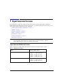
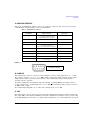
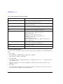
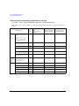
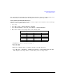
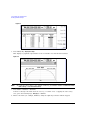
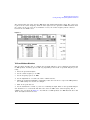
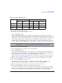
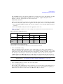
Table 1- 1 lists the available PSG signal generator models and frequency- range options.
Table 1-1 PSG Signal Generator Models
Model
Frequency Range Options
E8257D PSG analog signal generator
250
250
250
250
kHz
kHz
kHz
kHz
to
to
to
to
20 GHz (Option 520)
31.8 GHz (Option 532)
40 GHz (Option 540)
50 GHz (Option 550)
250 kHz to 67 GHza (Option 567)
E8267D PSG vector signal generator
250 kHz to 20 GHz (Option 520)
250 kHz to 31.8 GHz (Option 532)
250 kHz to 44 GHz (Option 544)
a.Instruments with Option 567 are functional, but unspecified, above 67 GHz to 70 GHz
Chapter 1
1
Signal Generator Overview
Signal Generator Models and Features
E8257D PSG Analog Signal Generator Features
The E8257D PSG includes the following standard features:
• CW output from 250 kHz to the highest operating frequency, depending on the option
• frequency resolution to 0.001 Hz
• list and step sweep of frequency and amplitude, with multiple trigger sources
• user flatness correction
• external diode detector leveling
• automatic leveling control (ALC) on and off modes; power calibration in ALC- off mode is
available, even without power search
• 10 MHz reference oscillator with external output
• RS- 232, GPIB, and 10Base- T LAN I/O interfaces
• a source module interface that is compatible with Agilent 83550 Series millimeter- wave source
modules for frequency extension up to 110 GHz and Oleson Microwave Labs (OML) AG- Series
millimeter- wave modules for frequency extensions up to 325 GHz
The E8257D PSG also offers the following optional features:
Option 007—analog ramp sweep
Option UNR/UNX—enhanced phase noise performance
Option UNT—AM, FM, phase modulation, and LF output
• open- loop or closed- loop AM
• dc- synthesized FM to 10 MHz rates; maximum deviation depends on the carrier frequency
• external modulation inputs for AM, FM, and ΦM
• simultaneous modulation configurations (except: FM with ΦM or Linear AM with
Exponential AM)
• dual function generators that include the following:
—
50- ohm low- frequency output, 0 to 3 Vp, available through the LF output
—
selectable waveforms: sine, dual- sine, swept- sine, triangle, positive ramp, negative ramp,
square, uniform noise, Gaussian noise, and dc
—
adjustable frequency modulation rates
—
selectable triggering in list and step sweep modes: free run (auto), trigger key (single), bus
(remote), and external
Option UNU—pulse modulation
• internal pulse generator
• external modulation inputs
• selectable pulse modes: internal square, internal free- run, internal triggered, internal doublet,
internal gated, and external pulse; internal triggered, internal doublet, and internal gated
2
Chapter 1
Signal Generator Overview
Signal Generator Models and Features
require an external trigger source
• adjustable pulse rate
• adjustable pulse period
• adjustable pulse width (150 ns minimum)
• adjustable pulse delay
• selectable external pulse triggering: positive or negative
Option UNW—narrow pulse modulation
• generate narrow pulses (20 ns minimum) across the operational frequency band of the PSG
• includes all the same functionality as Option UNU
Option 1EA—high output power
Option 1E1—step attenuator
Option 1ED—Type- N female RF output connector
Option 1EH—improved harmonics below 2 GHz
Option 1EM—moves all front panel connectors to the rear panel
E8267D PSG Vector Signal Generator Features
The E8267D PSG provides the same standard functionality as the E8257D PSG, plus the following:
• internal I/Q modulator
• external analog I/Q inputs
• single- ended and differential analog I/Q outputs
• high output power (optional for the E8257D)
• step attenuator (optional for the E8257D)
The E8267D PSG offers the same options as the E8257D PSG, plus the following:
Option 601 (Discontinued)—internal baseband generator with 8 megasamples of memory
Option 602—internal baseband generator with 64 megasamples of memory
Option 003—PSG digital output connectivity with N5102A
Option 004—PSG digital input connectivity with N5102A
Option 005—6 GB internal hard drive
Option 015—single- ended wideband external I/Q inputs (Discontinued)
Option 016—differential wideband external I/Q inputs
Chapter 1
3
Signal Generator Overview
Options
Options
PSG signal generators have hardware, firmware, software, and documentation options. The Data
Sheet shipped with your signal generator provides an overview of available options. For more
information, visit the Agilent PSG web page at http://www.agilent.com/find/psg, select the desired
PSG model, and then click the Options tab.
Firmware Upgrades
You can upgrade the firmware in your signal generator whenever new firmware is released. New
firmware releases, which can be downloaded from the Agilent website, may contain signal generator
features and functionality not available in previous firmware releases.
To determine the availability of new signal generator firmware, visit the Signal Generator Firmware
Upgrade Center web page at http://www.agilent.com/find/upgradeassistant, or call the number listed
at http://www.agilent.com/find/assist.
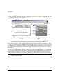
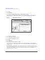
To Upgrade Firmware
The following procedure shows you how to download new firmware to your PSG using a LAN
connection and a PC. For information on equipment requirements and alternate methods of
downloading firmware, such as GPIB, refer to the Firmware Upgrade Guide, which can be accessed
at http://www.agilent.com/find/upgradeassistant.
1. Note the IP address of your signal generator. To view the IP address on the PSG, press Utility >
GPIB/RS-232 LAN > LAN Setup.
2. Use an internet browser to visit http://www.agilent.com/find/upgradeassistant.
3. Scroll down to the “Documents and Downloads” table and click the link in the “Latest Firmware
Revision” column for the E8257/67D PSG.
4. In the File Download window, select Run.
5. In the Welcome window, click Next and follow the on- screen instructions. The firmware files
download to the PC.
6. In the “Documents and Downloads” table, click the link in the “Upgrade Assistant Software”
column for the E8257/67D PSG to download the PSG/ESG Upgrade Assistant.
7. In the File Download window, select Run.
8. In the Welcome window, click OK and follow the on- screen instructions.
9. At the desktop shortcut prompt, click Yes.
10. Once the utility downloads, close the browser and double- click the PSG/ESG Upgrade Assistant icon on
the desktop.
11. In the upgrade assistant, set the connection type you wish to use to download the firmware, and
the parameters for the type of connection selected. For LAN, enter the instrument’s IP address,
which you recorded in step 1.
4
Chapter 1
Signal Generator Overview
Modes of Operation
NOTE
If the PSG’s dynamic host configuration protocol (DHCP) is enabled, the network assigns the
instrument an IP address at power on. Because of this, when DHCP is enabled, the IP
address may be different each time you turn on the instrument. DHCP does not affect the
hostname.
12. Click Browse, and double- click the firmware revision to upgrade your signal generator.
13. In the Upgrade Assistant, click Next.
14. Once connection to the instrument is verified, click Next and follow the on- screen prompts.
NOTE
Once the download starts, it cannot be aborted.
NOTE
When the User Attention message appears, you must first cycle the instrument’s power, then
click OK.
When the upgrade completes, the Upgrade Assistant displays a summary.
15. Click OK and close the Upgrade Assistant.
Modes of Operation
Depending on the model and installed options, the PSG signal generator provides up to four basic
modes of operation: continuous wave (CW), swept signal, analog modulation, and digital modulation.
Continuous Wave
In this mode, the signal generator produces a continuous wave signal. The signal generator is set to
a single frequency and power level. Both the E8257D and E8267D can produce a CW signal.
Swept Signal
In this mode, the signal generator sweeps over a range of frequencies and/or power levels. Both the
E8257D and E8267D provide list and step sweep functionality. Option 007 adds analog ramp sweep
functionality.
Analog Modulation
In this mode, the signal generator modulates a CW signal with an analog signal. The analog
modulation types available depend on the installed options.
Option UNT provides amplitude, frequency, and phase modulations. Some of these modulations can be
used together. Options UNU and UNW provide standard and narrow pulse modulation capability,
respectively.
Chapter 1
5
Signal Generator Overview
Modes of Operation
Digital Modulation
In this mode, the signal generator modulates a CW signal with either a real- time I/Q signal or
arbitrary I/Q waveform. I/Q modulation is only available on the E8267D. An internal baseband
generator (Option 601/602) adds the following digital modulation formats:
• Custom Arb Waveform Generator mode can produce a single- modulated carrier or
multiple- modulated carriers. Each modulated carrier waveform must be calculated and generated
before it can be output; this signal generation occurs on the internal baseband generator. Once a
waveform has been created, it can be stored and recalled, which enables repeatable playback of
test signals. To learn more, refer to “Custom Arb Waveform Generator” on page 143.
• Custom Real Time I/Q Baseband mode produces a single carrier, but it can be modulated with
real- time data that allows real- time control over all of the parameters that affect the signal. The
single- carrier signal that is produced can be modified by applying various data patterns, filters,
symbol rates, modulation types, and burst shapes. To learn more, refer to “Custom Real Time I/Q
Baseband” on page 165.
• Two Tone mode produces two separate continuous wave signals (or tones). The frequency spacing
between the two signals and the amplitudes are adjustable. To learn more, refer to “Two- Tone
Waveform Generator” on page 195.
• Multitone mode produces up to 64 continuous wave signals (or tones). Like Two Tone mode, the
frequency spacing between the signals and the amplitudes are adjustable. To learn more, refer to
“Multitone Waveform Generator” on page 185.
• Dual ARB mode is used to control the playback sequence of waveform segments that have been
written into the ARB memory located on the internal baseband generator. These waveforms can
be generated by the internal baseband generator using the Custom Arb Waveform Generator
mode, or downloaded through a remote interface into the ARB memory. To learn more, refer to
“Using the Dual ARB Waveform Player” on page 83.
6
Chapter 1
Signal Generator Overview
Front Panel
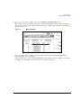
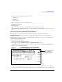
Front Panel
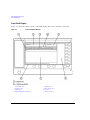
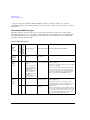
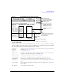
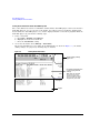
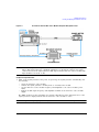
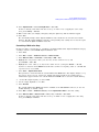
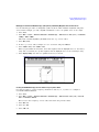
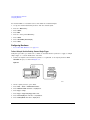
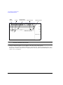
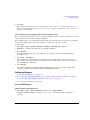
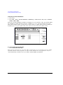
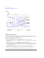
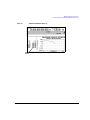
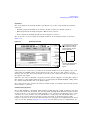
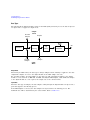
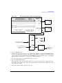
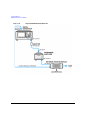
This section describes each item on the PSG front panel. Figure 1- 1 shows an E8267D front panel,
which includes all items available on the E8257D as well.
Figure 1-1
1.
2.
3.
4.
5.
6.
7.
8.
9.
Display
Softkeys
Knob
Amplitude
Frequency
Save
Recall
Trigger
MENUS
Chapter 1
Standard E8267D Front Panel Diagram
10.
11.
12.
13.
14.
15.
16.
17.
18.
Help
EXT 1 INPUT
EXT 2 INPUT
LF OUTPUT
Mod On/Off
ALC INPUT
RF On/Off
Numeric Keypad
RF OUTPUT
19.
20.
21.
22.
23.
24.
25.
26.
27.
SYNC OUT
VIDEO OUT
Incr Set
GATE/ PULSE/ TRIGGER INPUT
Arrow Keys
Hold
Return
Contrast Decrease
Contrast Increase
28.
29.
30.
31.
32.
33.
34.
35.
36.
37.
Local
Preset
Line Power LED
LINE
Standby LED
SYMBOL SYNC
DATA CLOCK
DATA
Q Input
I Input
7
Signal Generator Overview
Front Panel
1. Display
The LCD screen provides information on the current function. Information can include status
indicators, frequency and amplitude settings, and error messages. Softkeys labels are located on the
right- hand side of the display. For more detail on the front panel display, see “Front Panel Display”
on page 14.
2. Softkeys
Softkeys activate the displayed function to the left of each key.
3. Knob
Use the knob to increase or decrease a numeric value, change a highlighted digit or character, or step
through lists or select items in a row.
4. Amplitude
Pressing this hardkey makes amplitude the active function. You can change the output amplitude or
use the menus to configure amplitude attributes such as power search, user flatness, and leveling
mode.
5. Frequency
Pressing this hardkey makes frequency the active function. You can change the output frequency or
use the menus to configure frequency attributes such as frequency multiplier, offset, and reference.
6. Save
Pressing this hardkey displays a menu of choices that enable you to save data in the instrument state
register. The instrument state register is a section of memory divided into 10 sequences (numbered 0
through 9), each containing 100 registers (numbered 00 through 99). It is used to store and recall
frequency, amplitude, and modulation settings.
The Save hardkey provides a quick alternative to reconfiguring the signal generator through the front
panel or SCPI commands when switching between different signal configurations. Once an instrument
state has been saved, all of the frequency, amplitude, and modulation settings can be recalled with
the Recall hardkey. For more information on saving and recalling instrument states, refer to “Using the
Instrument State Registers” on page 57.
7. Recall
This key restores an instrument state saved in a memory register. To recall an instrument state, press
Recall and enter the desired sequence number and register number. To save a state, use the Save
hardkey. For more information on saving and recalling instrument states, refer to “Using the
Instrument State Registers” on page 57.
8
Chapter 1
Signal Generator Overview
Front Panel
8. Trigger
This key initiates an immediate trigger event for a function such as a list, step, or ramp sweep
(Option 007 only). Before this hardkey can be used to initiate a trigger event, the trigger mode must
be set to Trigger Key. For example: press the Sweep/List hardkey, then one of the following sequences
of softkeys:
• More (1 of 2) > Sweep Trigger > Trigger Key
• More (1 of 2) > Point Trigger > Trigger Key
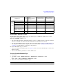
9. MENUS
These keys open softkey menus for configuring various functions. For descriptions, see the
E8257D/67D PSG Signal Generators Key Reference.
Table 1-2 Hardkeys in Front Panel MENUS Group
E8257D PSG Analog
AM
Sweep/List
FM/ΦM
Utility
Pulse
LF Out
NOTE
E8267D PSG Vector
Mode
Mux
AM
Sweep/List
Mode Setup
Aux Fctn
FM/ΦM
Utility
I/Q
Pulse
LF Out
Some menus are optional. Refer to “Options” on page 4 for more information.
10. Help
Pressing this hardkey causes a short description of any hardkey or softkey to be displayed and, in
most cases, a listing of related remote- operation SCPI commands. There are two help modes available
on the signal generator: single and continuous. The single mode is the factory preset condition.
Toggle between single and continuous mode by pressing Utility > Instrument Info/Help Mode > Help Mode
Single Cont.
• In single mode, help text is provided for the next key you press without activating the key’s
function. Any key pressed afterward exits the help mode and its function is activated.
• In continuous mode, help text is provided for each subsequent key press until you press the Help
hardkey again or change to single mode. In addition, each key is active, meaning that the key
function is executed (except for the Preset key).
11. EXT 1 INPUT
This female BNC input connector (functional only with Options UNT, UNU, or UNW) accepts a ±1 Vp
signal for AM, FM, and ΦM. For these modulations, ±1 Vp produces the indicated deviation or depth.
When ac- coupled inputs are selected for AM, FM, or ΦM and the peak input voltage differs from 1 Vp
by more than 3 percent, the HI/LO display annunciators light. The input impedance is selectable as
either 50 or 600 ohms; the damage levels are 5 Vrms and 10 Vp. On signal generators with Option
1EM, this connector is located on the rear panel.
Chapter 1
9
Signal Generator Overview
Front Panel
12. EXT 2 INPUT
This female BNC input connector (functional only with Options UNT, UNU, or UNW) accepts a ±1 Vp
signal for AM, FM, and ΦM. With AM, FM, or ΦM, ±1 Vp produces the indicated deviation or depth.
When ac- coupled inputs are selected for AM, FM, or ΦM and the peak input voltage differs from 1 Vp
by more than 3 percent, the HI/LO annunciators light on the display. The input impedance is
selectable as either 50 or 600 ohms and damage levels are 5 Vrms and 10 Vp. On signal generators
with Option 1EM, this connector is located on the rear panel.
13. LF OUTPUT
This female BNC output connector (functional only with Option UNT) outputs modulation signals
generated by the low frequency (LF) source function generator. This output is capable of driving
3Vp (nominal) into a 50 ohm load. On signal generators with Option 1EM, this connector is located
on the rear panel.
14. Mod On/Off
This hardkey (E8267D and E8257D with Options UNT, UNU, or UNW and E8267D only) enables or
disables all active modulation formats (AM, FM, ΦM, Pulse, or I/Q) applied to the output carrier
signal available through the RF OUTPUT connector. This hardkey does not set up or activate an AM,
FM, ΦM, Pulse, or I/Q format; each modulation format must still be set up and activated (for
example, AM > AM On) or nothing is applied to the output carrier signal when the Mod On/Off hardkey
is enabled. The MOD ON/OFF annunciator indicates whether active modulation formats have been
enabled or disabled with the Mod On/Off hardkey.
15. ALC INPUT
This female BNC input connector is used for negative external detector leveling. This connector
accepts an input of −0.2 mV to −0.5 V. The nominal input impedance is 120 kohms and the damage
level is ±15 V. On signal generators with Option 1EM, this connector is located on the rear panel.
16. RF On/Off
Pressing this hardkey toggles the operating state of the RF signal present at the RF OUTPUT
connector. Although you can set up and enable various frequency, power, and modulation states, the
RF and microwave output signal is not present at the RF OUTPUT connector until RF On/Off is set to
On. The RF On/Off annunciator is always visible in the display to indicate whether the RF is turned
on or off.
17. Numeric Keypad
The numeric keypad consists of the 0 through 9 hardkeys, a decimal point hardkey, and a backspace
hardkey (
). The backspace hardkey enables you to backspace or alternate between a positive
and a negative value. When specifying a negative numeric value, the negative sign must be entered
prior to entering the numeric value.
10
Chapter 1
Signal Generator Overview
Front Panel
18. RF OUTPUT
This connector outputs RF and microwave signals. The nominal output impedance is 50 ohms. The
reverse- power damage levels are 0 Vdc, 0.5 watts nominal. On signal generators with Option 1EM,
this connector is located on the rear panel. The connector type varies according to frequency option.
19. SYNC OUT
This female BNC output connector (functional only with Options UNU or UNW) outputs a
synchronizing TTL- compatible pulse signal that is nominally 50 ns wide during internal and triggered
pulse modulation. The nominal source impedance is 50 ohms. On signal generators with Option 1EM,
this connector is located on the rear panel.
20. VIDEO OUT
This female BNC output connector (functional only with Options UNU or UNW) outputs a TTL- level
compatible pulse signal that follows the output envelope in all pulse modes. The nominal source
impedance is 50 ohms. On signal generators with Option 1EM, this connector is located on the rear
panel.
21. Incr Set
This hardkey enables you to set the increment value of the current active function. The increment
value of the current active function appears in the active entry area of the display. Use the numeric
keypad, arrow hardkeys, or the knob to adjust the increment value.
22. GATE/ PULSE/ TRIGGER INPUT
This female BNC input connector (functional only with Options UNU or UNW) accepts an externally
supplied pulse signal for use as a pulse or trigger input. With pulse modulation, +1 V is on and 0 V
is off (trigger threshold of 0.5 V with a hysteresis of 10 percent; so 0.6 V would be on and 0.4 V
would be off). The damage levels are ±5 Vrms and 10 Vp. The nominal input impedance is 50 ohms.
On signal generators with Option 1EM, this connector is located on the rear panel.
23. Arrow Keys
These up and down arrow hardkeys are used to increase or decrease a numeric value, step through
displayed lists, or to select items in a row of a displayed list. Individual digits or characters may be
highlighted using the left and right arrow hardkeys. Once an individual digit or character is
highlighted, its value can be changed using the up and down arrow hardkeys.
24. Hold
Pressing this hardkey blanks the softkey label area and text areas on the display. Softkeys, arrow
hardkeys, the knob, the numeric keypad, and the Incr Set hardkey have no effect once this hardkey is
pressed.
Chapter 1
11
Signal Generator Overview
Front Panel
25. Return
Pressing this hardkey displays the previous softkey menu. It enables you to step back through the
menus until you reach the first menu you selected.
26. Contrast Decrease
Pressing this hardkey causes the display background to darken.
27. Contrast Increase
Pressing this hardkey causes the display background to lighten.
28. Local
Pressing this hardkey deactivates remote operation and returns the signal generator to front- panel
control.
29. Preset
Pressing this hardkey sets the signal generator to a known state (factory or user- defined).
30. Line Power LED
This green LED indicates when the signal generator power switch is set to the on position.
31. LINE
In the on position, this switch activates full power to the signal generator; in standby, it deactivates
all signal generator functions. In standby, the signal generator remains connected to the line power
and power is supplied to some internal circuits.
32. Standby LED
This yellow LED indicates when the signal generator power switch is set to the standby condition.
33. SYMBOL SYNC
This female BNC input connector is CMOS- compatible and accepts an externally supplied symbol sync
signal for use with the internal baseband generator (Option 601/602). The expected input is a 3.3 V
CMOS bit clock signal (which is also TTL compatible). SYMBOL SYNC might occur once per symbol or
be a single one- bit- wide pulse that is used to synchronize the first bit of the first symbol. The
maximum clock rate is 50 MHz. The damage levels are > +5.5 V and < −0.5V. The nominal input
impedance is not definable. SYMBOL SYNC can be used in two modes:
• When used as a symbol sync in conjunction with a data clock, the signal must be high during the
first data bit of the symbol. The signal must be valid during the falling edge of the data clock
signal and may be a single pulse or continuous.
12
Chapter 1
Signal Generator Overview
Front Panel
• When the SYMBOL SYNC itself is used as the (symbol) clock, the CMOS falling edge is used to
clock the DATA signal.
On signal generators with Option 1EM, this connector is located on the rear panel.
34. DATA CLOCK
This female BNC input connector is CMOS compatible and accepts an externally supplied data- clock
input signal to synchronize serial data for use with the internal baseband generator (Option 601/602).
The expected input is a 3.3 V CMOS bit clock signal (which is also TTL compatible) where the rising
edge is aligned with the beginning data bit. The falling edge is used to clock the DATA and SYMBOL
SYNC signals. The maximum clock rate is 50 MHz. The damage levels are > +5.5 V and < −0.5V. The
nominal input impedance is not definable. On signal generators with Option 1EM, this connector is
located on the rear panel.
35. DATA
This female BNC input connector (Options 601/602 only) is CMOS compatible and accepts an
externally supplied serial data input for digital modulation applications. The expected input is a 3.3 V
CMOS signal (which is also TTL compatible) where a CMOS high = a data 1 and a CMOS low = a data
0. The maximum input data rate is 50 Mb/s. The data must be valid on the falling edges of the data
clock (normal mode) or the on the falling edges of the symbol sync (symbol mode). The damage levels
are > +5.5 and < −0.5V. The nominal input impedance is not definable. On signal generators with
Option 1EM, this connector is located on the rear panel.
36. Q Input
This female BNC input connector (E8267D only) accepts the quadrature- phase (Q) component of an
externally supplied, analog, I/Q modulation. The in- phase (I) component is supplied through the I
INPUT. The signal level is
= 0.5 Vrms for a calibrated output level. The nominal input
impedance is 50 or 600 ohms. The damage level is 1 Vrms and 10 Vpeak. To activate signals applied to
the I and Q input connectors, press Mux > I/Q Source 1 or I/Q Source 2 and then select either Ext 50 Ohm or
Ext 600 Ohm. On signal generators with Option 1EM, these connectors are located on the rear panel.
37. I Input
This female BNC input connector (E8267D only) accepts the in- phase (I) component of an externally
supplied, analog, I/Q modulation. The quadrature- phase (Q) component is supplied through the Q
INPUT. The signal level is
= 0.5 Vrms for a calibrated output level. The nominal input
impedance is 50 or 600 ohms. The damage level is 1 Vrms and 10 Vpeak. To activate signals applied to
the I and Q input connectors, press Mux > I/Q Source 1 or I/Q Source 2 and then select either Ext 50 Ohm or
Ext 600 Ohm. On signal generators with Option 1EM, these connectors are located on the rear panel.
Chapter 1
13
Signal Generator Overview
Front Panel Display
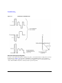
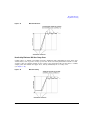
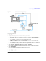
Front Panel Display
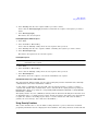
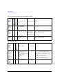
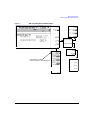
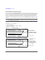
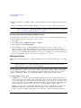
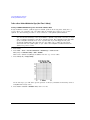
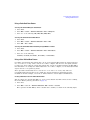
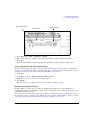
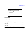
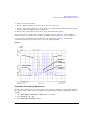
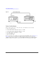
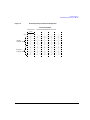
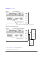
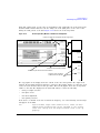
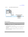
Figure 1- 2 shows the various regions of the PSG display. This section describes each region.
Figure 1-2
1.
2.
3.
4.
14
Front Panel Display Diagram
Active Entry Area
Frequency Area
Annunciators
Digital Modulation Annunciators
5.
6.
7.
8.
Amplitude Area
Error Message Area
Text Area
Softkey Label Area
Chapter 1
Signal Generator Overview
Front Panel Display
1. Active Entry Area
The current active function is shown in this area. For example, if frequency is the active function, the
current frequency setting will be displayed here. If the current active function has an increment value
associated with it, that value is also displayed.
2. Frequency Area
The current frequency setting is shown in this portion of the display. Indicators are also displayed in
this area when the frequency offset or multiplier is used, the frequency reference mode is turned on,
or a source module is enabled.
3. Annunciators
The display annunciators show the status of some of the signal generator functions and indicate any
error conditions. An annunciator position may be used by more than one function. This does not
create a problem, because only one function that shares an annunciator position can be active at a
time.
ΦM
This annunciator (Option UNT only) appears when phase modulation is on. If
frequency modulation is on, the FM annunciator replaces ΦM.
ALC OFF
This annunciator appears when the ALC circuit is disabled. A second annunciator,
UNLEVEL, appears in the same position if the ALC is enabled and cannot maintain
the output level.
AM
This annunciator (Option UNT only) appears when amplitude modulation is on.
ARMED
This annunciator appears when a sweep has been initiated and the signal
generator is waiting for the sweep trigger event.
ATTEN HOLD
This annunciator (E8267D or E8257D with Option 1E1 only) appears when the
attenuator hold function is on. When this function is on, the attenuator is held at
its current setting.
DIG BUS
This annunciator (Options 003/004 only) appears when the digital bus is active,
and the internal oven reference oscillator is not cold (OVEN COLD appears in this
same location).
ENVLP
This annunciator appears if a burst condition exists, such as when marker 2 is set
to enable RF blanking in the Dual ARB format.
ERR
This annunciator appears when an error message is in the error queue. This
annunciator does not turn off until you either view all the error messages or
cleared the error queue. To access error messages, press Utility > Error Info.
EXT
This annunciator appears when external leveling is on.
EXT1 LO/HI
This annunciator (Options UNT, UNU, or UNW only) appears as either EXT1 LO or
EXT1 HI, when the ac- coupled signal to the EXT 1 INPUT is < 0.97 Vp or
> 1.03 Vp.
EXT2 LO/HI
This annunciator (Options UNT, UNU, or UNW only) is displayed as either
EXT2 LO or EXT2 HI. This annunciator appears when the ac- coupled signal to the
EXT 2 INPUT is < 0.97 Vp or > 1.03 Vp.
Chapter 1
15
Signal Generator Overview
Front Panel Display
EXT REF
This annunciator appears when an external frequency reference is applied.
FM
This annunciator (Option UNT only) appears when frequency modulation is turned
on. If phase modulation is turned on, the ΦM annunciator will replace FM.
I/Q
This annunciator (E8267D only) appears when I/Q modulation is turned on.
L
This annunciator appears when the signal generator is in listener mode and is
receiving information or commands over the RS- 232, GPIB, or VXI- 11 LAN
interface.
MOD ON/OFF
This annunciator (E8267D and E8257D with Options UNT, UNU, or UNW only)
indicates whether active modulation formats have been enabled or disabled.
Pressing the Mod On/Off hardkey enables or disables all active modulation formats
(AM, FM, ΦM, Pulse, or I/Q) that are applied to the output carrier signal available
through the RF OUTPUT connector. The Mod On/Off hardkey does not set up or
activate an AM, FM, ΦM, Pulse, or I/Q format; each individual modulation format
must still be set up and activated (for example, AM > AM On) or nothing will be
applied to the output carrier signal when the Mod On/Off hardkey is enabled.
OVEN COLD
This annunciator (Option UNR/UNX only) appears when the temperature of the
internal oven reference oscillator has dropped below an acceptable level. When
this annunciator is on, frequency accuracy is degraded. This condition should
occur for several minutes after the signal generator is first connected to line
power.
PULSE
This annunciator (Options UNU or UNW only) appears when pulse modulation is
on.
R
This annunciator appears when the signal generator is remotely controlled over
the GPIB, RS- 232, or VXI- 11/Sockets LAN interface (TELNET operation does not
activate the R annunciator). When the R annunciator is on, the front panel keys
are disabled, except for the Local key and the line power switch. For information
on remote operation, refer to the Programming Guide.
RF ON/OFF
This annunciator indicates when the RF or microwave signal is present (RF ON) or
not present (RF OFF) at the RF OUTPUT. Either condition of this annunciator is
always visible in the display.
S
This annunciator appears when the signal generator has generated a service
request (SRQ) over the RS- 232, GPIB, or VXI- 11 LAN interface.
SWEEP
This annunciator appears when the signal generator is in list, step, or ramp sweep
mode (ramp sweep is available with Option 007 only). List mode is when the
signal generator can jump from point to point in a list (hop list); the list is
traversed in ascending or descending order. The list can be a frequency list, a
power level list, or both. Step mode is when a start, stop, and step value
(frequency or power level) are defined and the signal generator produces signals
that start at the start value and increment by the step value until it reaches the
stop value. Ramp sweep mode (Option 007 only) is when a start and stop value
(frequency or power level) are defined and the signal generator produces signals
that start at the start value and produce a continuous output until it reaches the
stop value.
T
This annunciator appears when the signal generator is in talker mode and is
transmitting information over the GPIB, RS- 232, or VXI- 11 LAN interface.
16
Chapter 1
Signal Generator Overview
Front Panel Display
UNLEVEL
This annunciator appears when the signal generator is unable to maintain the
correct output level. The UNLEVEL annunciator is not necessarily an indication of
instrument failure. Unleveled conditions can occur during normal operation. A
second annunciator, ALC OFF, will appear in the same position when the ALC
circuit is disabled.
UNLOCK
This annunciator appears when any of the phase locked loops are unable to
maintain phase lock. You can determine which loop is unlocked by examining the
error messages.
4. Digital Modulation Annunciators
All digital modulation annunciators (E8267D with Option 601/602 only) appear in this location. These
annunciators appear only when the modulation is active, and only one digital modulation can be
active at any given time.
ARB
Dual Arbitrary Waveform Generator
M-TONE
Multitone Waveform Generator
CUSTOM
Custom Real Time I/Q Baseband
T-TONE
Two- Tone Waveform Generator
DIGMOD
Custom Arb Waveform Generator
5. Amplitude Area
The current output power level setting is shown in this portion of the display. Indicators are also
displayed in this area when amplitude offset is used, amplitude reference mode is turned on, external
leveling mode is enabled, a source module is enabled, and when user flatness is enabled.
6. Error Message Area
Abbreviated error messages are reported in this space. When multiple error messages occur, only the
most recent message remains displayed. Reported error messages with details can be viewed by
pressing Utility > Error Info.
7. Text Area
This text area of the display:
• shows signal generator status information, such as the modulation status, sweep lists, and file
catalogs
• displays the tables
• enables you to perform functions such as managing information, entering information, and
displaying or deleting files
8. Softkey Label Area
The labels in this area define the function of the softkeys located immediately to the right of the
label. The softkey label may change depending upon the function selected.
Chapter 1
17
Signal Generator Overview
Rear Panel
Rear Panel
This section describes each item on the PSG rear panel. Four consecutive drawings show the
standard and Option 1EM rear panels for the E8267D and the E8257D. (Option 1EM moves all front
panel connectors to the real panel.)
Figure 1-3
1. EVENT 1
2. EVENT 2
3. PATTERN TRIG IN
4.
5.
6.
7.
8.
BURST GATE IN
AUXILIARY I/O
DIGITAL BUS
Q OUT
I OUT
9. WIDEBAND I INPUTS
10. I- bar OUT
18
Standard E8267D Rear Panel
11. WIDEBAND Q INPUTS
12. COH CARRIER
13. 1 GHz REF OUT (Serial Prefixes
>=US4646/MY4646)
14. Q- bar OUT
15. AC Power Receptacle
16. GPIB
17. 10 MHz EFC
18. ALC HOLD (Serial Prefixes
>=US4722/MY4722)
19. AUXILIARY INTERFACE
20. 10 MHz IN
21. LAN
22. 10 MHz OUT
23. STOP SWEEP IN/OUT
24.
25.
26.
27.
28.
BASEBAND GEN CLK IN
Z- AXIS BLANK/MKRS
SWEEP OUT
TRIGGER OUT
TRIGGER IN
29. SOURCE SETTLED
30. SOURCE MODULE INTERFACE
Chapter 1
Signal Generator Overview
Rear Panel
Figure 1-4
E8267D Option 1EM Rear Panel
1. EVENT 1
2. EVENT 2
3. PATTERN TRIG IN
4. BURST GATE IN
5. AUXILIARY I/O
6. DIGITAL BUS
7. Q OUT
8. I OUT
9. WIDEBAND I INPUTS
10. I- bar OUT
11. WIDEBAND Q INPUTS
12. COH CARRIER
13. 1 GHz REF OUT (Serial Prefixes
>=US4646/MY4646)
14. Q- bar OUT
15. AC Power Receptacle
Chapter 1
16.
17.
18.
19.
20.
21.
22.
23.
24.
25.
26.
27.
28.
GPIB
31. RF OUT
10 MHz EFC
32. EXT 1
ALC HOLD (Serial Prefixes >=US4722/MY4722) 33. EXT 2
AUXILIARY INTERFACE
34. PULSE SYNC OUT
10 MHz IN
35. PULSE VIDEO OUT
LAN
36. PULSE/TRIG GATE INPUT
10 MHz OUT
37. ALC INPUT
STOP SWEEP IN/OUT
38. DATA CLOCK
BASEBAND GEN CLK IN
39. I IN
Z- AXIS BLANK/MKRS
40. SYMBOL SYNC
SWEEP OUT
42. DATA
TRIGGER OUT
41. Q IN
TRIGGER IN
43. LF OUT
29. SOURCE SETTLED
30. SOURCE MODULE INTERFACE
19
Signal Generator Overview
Rear Panel
Figure 1-5
5. AUXILIARY I/O
12. COH CARRIER
15. AC Power Receptacle
16. GPIB
17. 10 MHz EFC
20
Standard E8257D Rear Panel
19.
20.
21.
22.
23.
AUXILIARY INTERFACE
10 MHz IN
LAN
10 MHz OUT
STOP SWEEP IN/OUT
25.
26.
27.
28.
29.
Z- AXIS BLANK/MKRS
SWEEP OUT
TRIGGER OUT
TRIGGER IN
SOURCE SETTLED
Chapter 1
Signal Generator Overview
Rear Panel
Figure 1-6
E8257D Option 1EM Rear Panel
5. AUXILIARY I/O
12. COH CARRIER
15. AC Power Receptacle
16. GPIB
17. 10 MHz EFC
19. AUXILIARY INTERFACE
20. 10 MHz IN
21. LAN
Chapter 1
22.
23.
25.
26.
27.
28.
31.
32.
10 MHz OUT
STOP SWEEP IN/OUT
Z- AXIS BLANK/MKRS
SWEEP OUT
TRIGGER OUT
TRIGGER IN
RF OUT
EXT 1
33.
34.
35.
36.
37.
43.
EXT 2
PULSE SYNC OUT
PULSE VIDEO OUT
PULSE/TRIG GATE INPUT
ALC INPUT
LF OUT
21
Signal Generator Overview
Rear Panel
1. EVENT 1
This female BNC connector is used with an internal baseband generator (Option 601/602). On signal
generators without Option 601/602, this female BNC connector is non- functional.
In real- time mode, the EVENT 1 connector outputs a pattern or frame synchronization pulse for
triggering or gating external equipment. It may be set to start at the beginning of a pattern, frame, or
timeslot and is adjustable to within ± one timeslot with one bit resolution.
In arbitrary waveform mode, the EVENT 1 connector outputs a timing signal generated by Marker 1.
A marker (3.3 V CMOS high for both positive and negative polarity) is output on the EVENT 1
connector whenever a Marker 1 is turned on in the waveform.
The reverse damage levels for this connector are > +8 V and < −4 V. The nominal output impedance
is not defined.
2. EVENT 2
This female BNC connector is used with an internal baseband generator (Option 601/602). On signal
generators without Option 601/602, this female BNC connector is non- functional.
In real- time mode, the EVENT 2 connector outputs a data enable signal for gating external
equipment. This is applicable when external data is clocked into internally generated timeslots. Data
is enabled when the signal is low.
In arbitrary waveform mode, the EVENT 2 connector outputs a timing signal generated by Marker 2.
A marker (3.3 V CMOS high for both positive and negative polarity) is output on the EVENT 2
connector whenever a Marker 2 is turned on in the waveform.
The reverse damage levels for this connector are > +8 V and < −4 V. The nominal output impedance
is not defined.
3. PATTERN TRIG IN
This female BNC connector is used with an internal baseband generator (Option 601/602). On signal
generators without Option 601/602, this female BNC connector is non- functional. This connector
accepts a signal that triggers an internal pattern or frame generator to start a single- pattern output.
Minimum pulse width is 100 ns. Damage levels are > +5.5 V and < −0.5 V. The nominal input
impedance is not defined.
4. BURST GATE IN
This female BNC connector is used with an internal baseband generator (Option 601/602). On signal
generators without Option 601/602, this connector is non- functional. This connector accepts a 3- volt
CMOS input signal for gating burst power. Burst gating is used when you are externally supplying
data and clock information.
The input signal must be synchronized with the external data input that will be output during the
burst. The burst power envelope and modulated data are internally delayed and re- synchronized. The
input signal must be CMOS high for normal burst RF power or CW RF output power and CMOS low
for RF off. Damage levels are > +5.5 V and < −0.5 V. The nominal input impedance is not defined.
22
Chapter 1
Signal Generator Overview
Rear Panel
5. AUXILIARY I/O
This female 37- pin connector is active only on instruments with an internal baseband generator
(Option 601/602); on signal generators without Option 601/602, this connector is non- functional. This
connector provides access to the inputs and outputs described in the following figure.
Figure 1-7
View looking into
rear panel connector
Auxiliary I/O Connector (Female 37-Pin)
EVENT 3: Used with an internal baseband generator. In arbitrary waveform mode,
this pin outputs a timing signal generated by Marker 3. A marker (3.3 V CMOS
high for both positive and negative polarity) is output on this pin when a Marker 3 is
turned on in the waveform. Reverse damage levels: > +8 V and < −4 V.
EVENT 4: Used with an internal baseband generator. In arbitrary
waveform mode, this pin outputs a timing signal generated by
Marker 4. A marker (3.3V CMOS high for both positive and
negative polarity) is output on this pin when a Marker 4 is turned
on in the waveform. Reverse damage levels: > +8 V and < −4 V.
PATT TRIG IN 2: Accepts a signal that triggers an
internal pattern or frame generator to start single
pattern output. Minimum pulse width: 100 ns.
Damage levels: > +5.5 V and < −0.5 V.
ALT PWR IN: Used with an internal baseband
generator. This pin accepts a CMOS signal for
synchronization of external data and alternate power
signal timing. Damage levels are > +8 V and < −4 V.
DATA OUT: Used with an internal baseband generator.
This pin outputs data (CMOS) from the internal data
generator or the externally supplied signal at data input.
DATA CLK OUT: Used with an internal baseband
generator. This pin relays a CMOS bit clock signal for
synchronizing serial data.
SYM SYNC OUT: Used with an internal baseband
generator. This pin outputs the CMOS symbol clock for
symbol synchronization, one data clock period wide.
Chapter 1
23
Signal Generator Overview
Rear Panel
6. DIGITAL BUS
This is a proprietary bus used for Agilent Baseband Studio products, which require an E8267D with
Options 003/004 and 601/602. This connector is not operational for general- purpose customer use.
Signals are present only when a Baseband Studio option is installed (for details, refer to
http://www.agilent.com/find/basebandstudio). The DIG BUS annunciator appears on the display when
the Digital Bus is active (and the internal oven reference oscillator is not cold—OVEN COLD appears in
this same location).
7. Q OUT
This female BNC connector (E8267D only) is used with an internal baseband generator
(Option 601/602) to output the analog, quadrature- phase component of I/Q modulation. On signal
generators without Option 601/602, this female BNC connector is used to output the
quadrature- phase component of an external I/Q modulation that has been fed into the Q input
connector. The nominal output impedance of the Q OUT connector is 50 ohms, dc- coupled.
8. I OUT
This female BNC connector (E8267D only) is used with an internal baseband generator
(Option 601/602) to output the analog, in- phase component of I/Q modulation. On signal generators
without Option 601/602, this female BNC connector is used to output the in- phase component of an
external I/Q modulation that has been fed into the I input connector. The nominal output impedance
of the I OUT connector is 50 ohms, dc- coupled.
9. WIDEBAND I INPUTS
These female SMA connectors: I IN (+) and I- bar IN (−) (Option 016 only) are used with differential
wideband external I/Q inputs. They accept wideband AM and allow direct high–bandwidth analog
inputs to the I/Q modulator in the 3.2−44 GHz range (frequency limit is dependant on the option).
This input is not calibrated. The recommended input power level is −1 dBm with a +/− 1 VDC input
voltage. The nominal impedance for this connector is 50 ohms.
The signal generator uses lowside mixing in the 20–28.5 GHz frequency range (Options 532 and 544),
which reverses the phase relationship for I and Q signals. For internally generated I/Q signals the
signal generator’s firmware compensates for this. However, for wideband external I/Q inputs
(Option 016) there is no compensation and the I and Q inputs at the rear panel must be reversed to
maintain the correct phase relationships in this frequency band. Refer to the Data Sheet and to the
A37 Upconverter description in the Service Guide for more information.
For instruments with Option 015 (discontinued), single- ended wideband I/Q, there is a single BNC I
input. The recommended power level at this input connector is 0 dBM.
24
Chapter 1
Signal Generator Overview
Rear Panel
10. I-bar OUT
This female BNC connector (E8267D only) is used with an internal baseband generator
(Option 601/602) to output the complement of the analog, in- phase component of I/Q modulation. On
signal generators without Option 601/602, this female BNC connector is used to output the
complement of the in- phase component of an external I/Q modulation that has been fed into the
I input connector.
I- bar OUT is used in conjunction with I OUT to provide a balanced baseband stimulus. Balanced
signals are signals present in two separate conductors that are symmetrical relative to ground and
are opposite in polarity (180 degrees out of phase). The nominal output impedance of the I- bar OUT
connector is 50 ohms, dc- coupled.
11. WIDEBAND Q INPUTS
These female SMA connectors: Q IN (+) and Q- bar IN (−) (Option 016 only) are used with differential
wideband external I/Q inputs. They accept wideband AM and allow direct high–bandwidth analog
inputs to the I/Q modulator in the 3.2−44 GHz range (frequency limit is dependant on the option).
This input is not calibrated. The recommended input power level is −1 dBm with a +/− 1 VDC input
voltage. The nominal impedance for this connector is 50 ohms.
The signal generator uses lowside mixing in the 20–28.5 GHz frequency range (Options 532 and 544),
which reverses the phase relationship for I and Q signals. For internally generated I/Q signals the
signal generator’s firmware compensates for this. However, for wideband external I/Q inputs
(Option 016) there is no compensation and the I and Q inputs at the rear panel must be reversed to
maintain the correct phase relationships in this frequency band. Refer to the Data Sheet and to the
A37 Upconverter description in the Service Guide for more information.
For instruments with Option 015 (discontinued), single- ended wideband I/Q, there is a single BNC Q
input. The recommended power level at this input connector is 0 dBM.
12. COH CARRIER
This female SMA connector (Option UNT only) outputs an RF signal that is phase coherent with the
signal generator carrier. The coherent carrier connector outputs RF that is not modulated with AM,
pulse, or I/Q modulation, but is modulated with FM or ΦM (when FM or ΦM are on).
The output power is nominally 0 dBm. The output frequency range is from 249.99900001 MHz to
3.2 GHz; this output is not useful for output frequencies > 3.2 GHz. If the RF output frequency is
below 249.99900001 MHz, the coherent carrier output signal will have the following frequency:
Frequency of coherent carrier = (1E9 − Frequency of RF output) in Hz.
Damage levels are 20 Vdc and 13 dBm reverse RF power. The nominal output impedance of this
connector is 50 ohms.
13. 1 GHz REF OUT (Serial Prefixes >=US4646/MY4646)
This female SMA connector (Option UNX only) provides a 1 GHz output that is 100 times the
frequency of the internal or external 10 MHz reference. The nominal output level is 7 dBM. The
nominal output impedance is 50 ohms. When not in use, this connector must be terminated with a
50 ohm load.
Chapter 1
25
Signal Generator Overview
Rear Panel
14. Q-bar OUT
This female BNC connector (E8267D only) can be used with an internal baseband generator
(Option 601/602) to output the complement of the analog, quadrature- phase component of I/Q
modulation. On signal generators without Option 601/602, this female BNC connector can be used to
output the complement of the quadrature- phase component of an external I/Q modulation that has
been fed into the Q input connector.
Q- bar OUT is used in conjunction with Q OUT to provide a balanced baseband stimulus. Balanced
signals are signals present in two separate conductors that are symmetrical relative to ground and
are opposite in polarity (180 degrees out of phase). The nominal output impedance of the Q- bar OUT
connector is 50 ohms, dc- coupled.
15. AC Power Receptacle
The ac line voltage is connected here. The power cord receptacle accepts a three- pronged power cable
that is shipped with the signal generator.
16. GPIB
This GPIB interface allows listen and talk capability with compatible IEEE 488.2 devices.
17. 10 MHz EFC
This female BNC input connector (Options UNR/UNX only) accepts an external dc voltage, ranging
from −5 V to +5 V, for electronic frequency control (EFC) of the internal 10 MHz reference oscillator.
This voltage inversely tunes the oscillator about its center frequency (approximately −0.0025 ppm/V).
The nominal input impedance is greater than 1 Mohms. When not in use, this connector should be
shorted using the supplied shorting cap to assure a stable operating frequency.
18. ALC HOLD (Serial Prefixes >=US4722/MY4722)
This female BNC connector (E8267D only) is a TTL- compatible input that controls ALC action with
bursted I/Q signals from an arbitrary waveform generator (AWG). A high signal allows the ALC to
track the RF signal and maintain constant RF output level as the I/Q inputs vary. A low input signal
allows the ALC to be held for a brief time (less than 1 second) and not track the RF signal. When
driving the external I/Q inputs from an external arbitrary waveform generator supplying a bursted
waveform, the ALC Hold line should be driven from a marker output from the AWG that is high when
the bursted signal is at the proper level and low when the bursted signal is not at the proper level
Damage levels are > 5.5 V and < −0.5 V.
26
Chapter 1
Signal Generator Overview
Rear Panel
19. AUXILIARY INTERFACE
This 9- pin D- subminiature female connector is an RS- 232 serial port that can be used for serial
communication and Master/Slave source synchronization.
Table 1-3 Auxiliary Interface Connector
Pin Number
Signal Description
Signal Name
1
No Connection (default operation)/
Retrace (Master/Slave operation)
2
Receive Data
RECV
3
Transmit Data
XMIT
4
+5V (Default operation)/
Sweep Stop (Master/Slave operation)
5
Ground, 0V
6
No Connection
7
Request to Send
RTS
8
Clear to Send
CTS
9
No Connection
Figure 1-8
View looking into
rear panel connector
20. 10 MHz IN
This female BNC connector accepts an external timebase reference input signal level of > −3 dBm.
The reference must be 1, 2, 2.5, 5, or 10 MHz, within ±1 ppm. The signal generator detects when a
valid reference signal is present at this connector and automatically switches from internal to
external reference operation.
For Option UNR/UNX or instruments with serial prefixes > US4805/MY4805, this BNC connector
accepts a signal with a nominal input level of 5 ±5 dBm. The external frequency reference must be
10 MHz, within ±1 ppm.
The nominal input impedance is 50 ohms with a damage level of ≥ 10 dBm.
21. LAN
This LAN interface allows ethernet local area network communication through a 10Base- T LAN cable.
The yellow LED on the interface illuminates when data transmission (transfer/receive) is present. The
green LED illuminates when there is a delay in data transmission or no data transmission is present.
Chapter 1
27
Signal Generator Overview
Rear Panel
22. 10 MHz OUT
This female BNC connector outputs a nominal signal level of > +4 dBm and has an output impedance
of 50 ohms. The accuracy is determined by the timebase used.
23. STOP SWEEP IN/OUT
This female BNC connector (Option 007 only) provides an open- collector, TTL- compatible
input/output signal that is used during ramp sweep operation. It provides low- level (nominally 0 V)
output during sweep retrace and band- cross intervals. It provides high- level (nominally +5 V) output
during the forward portion of the sweep. Sweep stops when this input/output connector is grounded
externally. When operating as an input, the nominal impedance for this connector is less than
10 ohms. When operating as an output, the nominal impedance is approximately 4.2 kohms.
24. BASEBAND GEN CLK IN
This female BNC connector accepts a sine or square wave PECL clock input with a frequency range
of 200 MHz to 400 MHz, resulting in sample rates of 50 MSa/s to 100 MSa/s. The recommended input
level is approximately 1 Vpeak- to- peak for a square wave and 1 dBm to 6 dBm for a sine wave. This
allows baseband generators from multiple signal sources to run off the same clock.
25. Z-AXIS BLANK/MKRS
This female BNC connector (Option 007 only) supplies a +5 V (nominal) level during retrace and
band- switch intervals of a step, list, or ramp sweep. During ramp sweep, this female BNC connector
supplies a –5 V (nominal) level when the RF frequency is at a marker frequency and intensity marker
mode is on. This signal is derived from an operational amplifier output so the load impedance should
be greater than or equal to 5 kohms. This connection is most commonly used to interface with an
Agilent 8757D Scalar Network Analyzer.
26. SWEEP OUT
This female BNC connector outputs a voltage proportional to the RF power or frequency sweep
ranging from 0 V at the start of sweep and goes to +10 V (nominal) at the end of sweep, regardless
of sweep width.
The nominal output impedance is less than 1 ohm and can drive a 2 kohm load.
When connected to an Agilent Technologies 8757D network analyzer, it generates a selectable number
of equally spaced 1 ms, 10 V pulses (nominal) across a ramp (analog) sweep. The number of pulses
can be set from 101 to 1601 by remote control through the 8757D.
28
Chapter 1
Signal Generator Overview
Rear Panel
27. TRIGGER OUT
This female BNC connector, in step/list sweep mode, outputs a TTL signal that is high at the start of
a dwell sequence or when waiting for a point trigger in manual sweep mode. The signal is low when
the dwell is over or when a point trigger is received. In ramp sweep mode, the output provides 1601
equally spaced 1 μs pulses (nominal) across a ramp sweep. When using LF Out, the output provides
a 2 μs pulse at the start of an LF sweep. The nominal impedance for this connector is less than
10 ohms.
28. TRIGGER IN
This female BNC connector accepts a 3.3V CMOS signal, which is used for point- to- point triggering in
manual sweep mode, or in a low frequency (LF output) or analog (AM, FM, and ΦM) external sweep
trigger setup. Triggering can occur on either the positive or negative edge of the signal start. The
damage level is ≤ −4 V or ≥ +10 V. The nominal input impedance for this connector is approximately
4.2 kohms.
29. SOURCE SETTLED
This female BNC connector provides a 3- volt CMOS output trigger, indicating when the signal
generator has settled to a new frequency or power level. A high indicates that the source has not
settled. A low indicates that the source has settled. The nominal output impedance for this connector
is less than 10 ohms.
30. SOURCE MODULE INTERFACE
This interface is used to connect to compatible Agilent Technologies 83550 Series mm- wave source
modules.
31. RF OUT
This connector outputs RF and microwave signals. The nominal output impedance is 50 ohms. The
reverse power damage levels are 0 Vdc, 0.5 watts nominal. On signal generators without Option 1EM,
this connector is located on the front panel. The connector type varies according to frequency option.
32. EXT 1
This female BNC input connector (functional only with Options UNT, UNU, or UNW) accepts a ±1 Vp
signal for AM, FM, and ΦM. For these modulations, ±1 Vp produces the indicated deviation or depth.
When ac- coupled inputs are selected for AM, FM, or ΦM and the peak input voltage differs from 1 Vp
by more than 3 percent, the HI/LO display annunciators light. The input impedance is selectable as
either 50 or 600 ohms; the damage levels are 5 Vrms and 10 Vp. On signal generators without Option
1EM, this connector is located on the front panel.
Chapter 1
29
Signal Generator Overview
Rear Panel
33. EXT 2
This female BNC input connector (functional only with Options UNT, UNU, or UNW) accepts a ±1 Vp
signal for AM, FM, and ΦM. With AM, FM, or ΦM, ±1 Vp produces the indicated deviation or depth.
When ac- coupled inputs are selected for AM, FM, or ΦM and the peak input voltage differs from 1 Vp
by more than 3 percent, the HI/LO annunciators light on the display. The input impedance is
selectable as either 50 or 600 ohms and damage levels are 5 Vrms and 10 Vp. On signal generators
without Option 1EM, this connector is located on the front panel.
34. PULSE SYNC OUT
This female BNC output connector (functional only with Options UNU or UNW) outputs a
synchronizing TTL- compatible pulse signal that is nominally 50 ns wide during internal and triggered
pulse modulation. The nominal source impedance is 50 ohms. On signal generators without Option
1EM, this connector is located on the front panel.
35. PULSE VIDEO OUT
This female BNC output connector (functional only with Options UNU or UNW) outputs a TTL- level
compatible pulse signal that follows the output envelope in all pulse modes. The nominal source
impedance is 50 ohms. On signal generators without Option 1EM, this connector is located on the
front rear panel.
36. PULSE/TRIG GATE INPUT
This female BNC input connector (functional only with Options UNU or UNW) accepts an externally
supplied pulse signal for use as a pulse or trigger input. With pulse modulation, +1 V is on and 0 V
is off (trigger threshold of 0.5 V with a hysteresis of 10 percent; so 0.6 V would be on and 0.4 V
would be off). The damage levels are ±5 Vrms and 10 Vp. The nominal input impedance is 50 ohms.
On signal generators without Option 1EM, this connector is located on the front panel.
37. ALC INPUT
This female BNC input connector is used for negative external detector leveling. This connector
accepts an input of −0.2 mV to −0.5 V. The nominal input impedance is 120 kohms and the damage
level is ±15 V. On signal generators without Option 1EM, this connector is located on the front panel.
38. DATA CLOCK
This female BNC input connector (E8267D only) is CMOS compatible and accepts an externally
supplied data clock input signal to synchronize serial data for use with the internal baseband
generator (Option 601/602). The expected input is a 3.3 V CMOS bit clock signal (which is also TTL
compatible) where the rising edge is aligned with the beginning data bit. The falling edge is used to
clock the DATA and SYMBOL SYNC signals. The maximum clock rate is 50 MHz. The damage levels
are > +5.5 V and < −0.5V. The nominal input impedance is not defined. On signal generators without
Option 1EM, this connector located on the front panel.
30
Chapter 1
Signal Generator Overview
Rear Panel
39. I IN
This female BNC input connector (E8267D only) accepts the in- phase (I) component an externally
supplied, analog, I/Q modulation. The quadrature- phase (Q) component is supplied through the Q IN
connector. The signal level is
= 0.5 Vrms for a calibrated output level. The nominal input
impedance is 50 or 600 ohms. The damage level is 1 Vrms and 10 Vpeak. To activate signals applied to
the I and Q input connectors, press Mux > I/Q Source 1 or I/Q Source 2 and then select either Ext 50 Ohm or
Ext 600 Ohm. On signal generators without Option 1EM, this connector is located on the front panel.
40. SYMBOL SYNC
This female BNC input connector (E8267D only) is CMOS- compatible and accepts an externally
supplied symbol sync signal for use with the internal baseband generator (Option 601/602). The
expected input is a 3.3 V CMOS bit clock signal (which is also TTL compatible). SYMBOL SYNC might
occur once per symbol or be a single one- bit- wide pulse that is used to synchronize the first bit of
the first symbol. The maximum clock rate is 50 MHz. The damage levels are > +5.5 V and < −0.5V.
The nominal input impedance is not defined. SYMBOL SYNC can be used in two modes:
• When used as a symbol sync in conjunction with a data clock, the signal must be high during the
first data bit of the symbol. The signal must be valid during the falling edge of the data clock
signal and may be a single pulse or continuous.
• When the SYMBOL SYNC itself is used as the (symbol) clock, the CMOS falling edge is used to
clock the DATA signal.
On signal generators without Option 1EM, this connector is located on the front panel.
41. Q IN
This female BNC input connector (E8267D only) accepts the quadrature- phase (Q) component an
externally supplied, analog, I/Q modulation. The in- phase (I) component is supplied through the I IN
connector. The signal level is
= 0.5 Vrms for a calibrated output level. The nominal input
impedance is 50 or 600 ohms. The damage level is 1 Vrms and 10 Vpeak. To activate signals applied to
the I and Q input connectors, press Mux > I/Q Source 1 or I/Q Source 2 and then select either Ext 50 Ohm or
Ext 600 Ohm. On signal generators without Option 1EM, this connector is located on the front panel.
42. DATA
This female BNC input connector (Option 601/602 only) is CMOS compatible and accepts an
externally supplied serial data input for digital modulation applications. The expected input is a 3.3 V
CMOS signal (which is also TTL compatible) where a CMOS high = a data 1 and a CMOS low = a data
0. The maximum input data rate is 50 Mb/s. The data must be valid on the falling edges of the data
clock (normal mode) or the on the falling edges of the symbol sync (symbol mode). The damage levels
are > +5.5 and < −0.5V. The nominal input impedance is not defined. On signal generators without
Option 1EM, this connector is located on the front panel.
Chapter 1
31
Signal Generator Overview
Rear Panel
43. LF OUT
This female BNC output connector (functional only with Option UNT) outputs modulation signals
generated by the low frequency (LF) source function generator. This output is capable of driving
3Vp (nominal) into a 50- ohm load. On signal generators without Option 1EM, this connector is
located on the front panel.
32
Chapter 1
2
Basic Operation
In the following sections, this chapter describes operations common to all Agilent PSG signal
generators:
• “Using Table Editors” on page 34
• “Configuring a Continuous Wave RF Output” on page 36
• “Configuring a Swept RF Output” on page 38
• “Using Ramp Sweep (Option 007)” on page 43
• “Extending the Frequency Range” on page 53
• “Turning On a Modulation Format” on page 53
• “Applying a Modulation Format to the RF Output” on page 54
• “Using Data Storage Functions” on page 55
• “Using the Instrument State Registers” on page 57
• “Using Security Functions” on page 59
• “Enabling Options” on page 66
• “Using the Web Server” on page 67
Chapter 2
33
Basic Operation
Using Table Editors
Using Table Editors
Table editors simplify configuration tasks, such as creating a list sweep. This section provides
information to familiarize you with basic table editor functionality using the List Mode Values table
editor as an example.
Press Preset > Sweep/List > Configure List Sweep.
The signal generator displays the List Mode Values table editor, as shown below.
Figure 2-1
Active Function Area
Table Name
Cursor
Table Items
Table Softkeys
Active Function Area
displays the active table item while its value is edited
Cursor
an inverse video identifier used to highlight specific table items
for selection and editing
Table Softkeys
select table items, preset table values, and modify table
structures
Table Items
values arranged in numbered rows and titled columns (The
columns are also known as data fields. For example, the
column below the Frequency title is known as the Frequency
data field).
34
Chapter 2
Basic Operation
Using Table Editors
Table Editor Softkeys
The following table editor softkeys are used to load, navigate, modify, and store table item values.
Edit Item
displays the selected item in the active function area of the display where the
item’s value can be modified
Insert Row
inserts an identical row of table items above the currently selected row
Delete Row
deletes the currently selected row
Goto Row
opens a menu of softkeys (Enter, Goto Top Row, Goto Middle Row, Goto Bottom Row, Page Up,
and Page Down) used to quickly navigate through the table items
Insert Item
inserts an identical item in a new row below the currently selected item
Delete Item
deletes the currently selected item
Page Up and
Page Down
displays table items that occupy rows outside the limits of the ten- row table
display area
More (1 of 2)
accesses Load/Store and its associated softkeys
Load/Store
opens a menu of softkeys (Load From Selected File, Store To File, Delete File, Goto Row, Page Up,
and Page Down) used to load table items from a file in the memory catalog, or to
store the current table items as a file in the memory catalog
Modifying Table Items in the Data Fields
1. If not already displayed, open the List Mode Values table editor (Figure 2- 1 on page 34):
Press Preset > Sweep/List > Configure List Sweep
2. Use the arrow keys or the knob to move the table cursor over the desired item.
In Figure 2- 1, the first item in the Frequency data field is selected.
3. Press Edit Item.
The selected item is displayed in the active function area of the display.
4. Use the knob, arrow keys, or the numeric keypad to modify the value.
5. Press Enter.
The modified item is now displayed in the table.
Chapter 2
35
Basic Operation
Configuring the RF Output
Configuring the RF Output
This section provides information on how to create continuous wave and swept RF (page 38) outputs.
It also has information on using a mm- Wave source module to extend the signal generator’s
frequency range (page 53).
Configuring a Continuous Wave RF Output
These procedures demonstrate how to set the following parameters:
•
•
•
•
RF output frequency
frequency reference and frequency offset (page 37)
RF output amplitude (page 37)
amplitude reference and amplitude offset (page 38)
Setting the RF Output Frequency
Set the RF output frequency to 700 MHz, and increment or decrement the output frequency in 1 MHz
steps.
1. Return the signal generator to the factory- defined state: Press Preset.
NOTE
You can change the preset condition of the signal generator to a user- defined state. For
these examples, however, use the factory- defined preset state (set the Preset Normal User softkey
in the Utility menu to Normal).
2. Observe the FREQUENCY area of the display (in the upper left- hand corner).
The value displayed is the maximum specified frequency of the signal generator.
3. Press RF On/Off.
The RF On/Off hardkey must be pressed before the RF signal is available at the
RF OUTPUT connector. The display annunciator changes from RF OFF to RF ON. The maximum
specified frequency should be output at the RF OUTPUT connector (at the signal generator’s
minimum power level).
4. Press Frequency > 700 > MHz.
The 700 MHz RF frequency should be displayed in the FREQUENCY area of the display and also in
the active entry area.
5. Press Frequency > Incr Set > 1 > MHz.
This changes the frequency increment value to 1 MHz.
6. Press the up arrow key.
Each press of the up arrow key increases the frequency by the increment value last set with the
Incr Set hardkey. The increment value is displayed in the active entry area.
7. The down arrow decreases the frequency by the increment value set in the previous step. Practice
stepping the frequency up and down in 1 MHz increments.
You can also adjust the RF output frequency using the knob. As long as frequency is the active
function (the frequency is displayed in the active entry area), the knob will increase and decrease
the RF output frequency.
36
Chapter 2
Basic Operation
Configuring the RF Output
8. Use the knob to adjust the frequency back to 700 MHz.
Setting the Frequency Reference and Frequency Offset
The following procedure sets the RF output frequency as a reference frequency to which all other
frequency settings are relative. When the frequency reference is set, the display will read 0.00 Hz
(the frequency output of the signal generator’s hardware minus the reference frequency). Although
the display changes, the actual frequency output is 700 MHz (from step 8 above). Any subsequent
frequency changes are shown as increments or decrements to the 0 Hz reference.
The Frequency Reference Set function is not an active function. Once it is set, any change to the
frequency setting appears as a frequency reading on the signal generator’s front- panel display. For
example,
1. Preset the signal generator: Press Preset.
2. Set the frequency reference to 700 MHz:
Press: Frequency > 700 > MHz > More (1 of 3) > Freq Ref Set.
This activates the frequency reference mode, sets the output frequency (700 MHz) as the reference
value, and toggles the Freq Ref softkey On. The FREQUENCY area displays 0.000 Hz. This reading is
the frequency output of the signal generator’s hardware (700 MHz) minus the reference value
(700 MHz). The signal generator’s true output frequency is 700 MHz. If the Freq Ref softkey is
toggled to Off, the front- panel will indicate the actual frequency: 700 MHz. The REF indicator
appears on the front- panel display and the Freq Ref Off On softkey toggles to On.
3. Turn on the RF output: Press RF On/Off.
The display annunciator changes from RF OFF to RF ON. The RF frequency at the RF OUTPUT
connector is 700 MHz.
4. Set the frequency increment value to 1 MHz: Press Frequency > Incr Set > 1 > MHz.
5. Increment the output frequency by 1 MHz: Press the up arrow key.
The FREQUENCY area display changes to show 1.000 000 000 MHz, which is the frequency output
by the hardware (700 MHz + 1 MHz) minus the reference frequency (700 MHz). The frequency at
the RF OUTPUT changes to 701 MHz.
6. Enter a 1 MHz offset: Press More (1 of 3) > Freq Offset > 1 > MHz.
The FREQUENCY area displays 2.000 000 00 MHz, which is the frequency output by the hardware
(701 MHz) minus the reference frequency (700 MHz) plus the offset (1 MHz). The OFFS indicator
activates. The frequency at the RF OUTPUT connector is still 701 MHz.
Setting the RF Output Amplitude
1. Preset the signal generator: Press Preset.
The AMPLITUDE area of the display shows the minimum power level of the signal generator. This
is the normal preset RF output amplitude.
2. Turn on the RF output: Press RF On/Off.
The display annunciator changes to RF ON. At the RF OUTPUT connector, the RF signal is output
at the minimum power level.
Chapter 2
37
Basic Operation
Configuring the RF Output
3. Change the amplitude to −20 dBm: Press Amplitude > −20 > dBm.
The new output power displays in the AMPLITUDE area of the display and in the active entry area.
Until you press a different front panel function key, amplitude remains the active function. You
can also change the amplitude using the up and down arrow keys or the knob.
Setting the Amplitude Reference and Amplitude Offset
The following procedure sets the RF output power as an amplitude reference to which all other
amplitude parameters are relative. The amplitude initially shown on the display is 0 dB (the power
output by the hardware minus the reference power). Although the display changes, the output power
does not change. Any subsequent power changes are shown as incremental or decremental to 0 dB.
1. Press Preset.
2. Set the amplitude to −20 dBm: Press Amplitude > -20 > dBm.
3. Activate the amplitude reference mode and set the current output power (−20 dBm) as the
reference value: Press More (1 of 2) > Ampl Ref Set.
The AMPLITUDE area displays 0.00 dB, which is the power output by the hardware (−20 dBm)
minus the reference value (−20 dBm). The REF indicator activates and the Ampl Ref Off On softkey
toggles On.
4. Turn the RF output on: Press RF On/Off.
The display annunciator changes to RF ON. The power at the RF OUTPUT connector is −20 dBm.
5. Change the amplitude increment value to 10 dB: Press Incr Set > 10 > dB.
6. Use the up arrow key to increase the output power by 10 dB.
The AMPLITUDE area displays 10.00 dB, which is the power output by the hardware
(- 20 dBm plus 10 dBm) minus the reference power (−20 dBm). The power at the RF OUTPUT
connector changes to −10 dBm.
7. Enter a 10 dB offset: Press Ampl Offset > 10 > dB.
The AMPLITUDE area displays 20.00 dB, which is the power output by the hardware (−10 dBm)
minus the reference power (−20 dBm) plus the offset (10 dB). The OFFS indicator activates. The
power at the RF OUTPUT connector is still −10 dBm.
Configuring a Swept RF Output
A PSG signal generator has up to three sweep types: step sweep, list sweep, and ramp sweep
(Option 007).
The signal generator indicates the sweep advance in a progress bar on the front- panel display. If the
sweep time is greater than one second, the progress bar sweep advances according to the frequency
span of each segment. For each segment in the span, the progress bar displays the full segment and
then the sweep is taken. With sweep times less than one second, the progress bar is drawn, the
sweep taken, and the progress bar is then blanked.
38
Chapter 2
Basic Operation
Configuring the RF Output
NOTE
List sweep data cannot be saved within an instrument state, but can be saved to the
memory catalog. For instructions on saving list sweep data, see “Storing Files to the Memory
Catalog” on page 56.
During swept RF output, the FREQUENCY and AMPLITUDE areas of the signal generator’s
display are deactivated, depending on what is being swept.
Step sweep (see page 39) and ramp sweep (see page 41) provide a linear progression through the
start- to- stop frequency and/or amplitude values, while list sweep enables you to create a list of
arbitrary frequency, amplitude, and dwell time values and sweep the RF output based on that list.
The list sweep example uses the points created in the step sweep example as the basis for a new list
sweep.
Ramp sweep (see page 43) is faster than step or list sweep, and is designed to work with an 8757D
Scalar Network Analyzer.
The signal generator provides a softkey, Sweep Retrace Off On, that lets you configure single sweep
behavior. When sweep retrace is on, the signal generator will retrace the sweep to the first point of
the sweep. If the sweep retrace is off, the sweep will stop and remain on the last point in the sweep.
Activating Scalar Pulse in Sweep Configurations
If your sweep setup uses a scalar network analyzer and a DC detector, the PSG must modulate the
swept signal with a 27 kHz square wave, also referred to as a scalar pulse. This pulse modulation is
necessary for the DC detector to properly detect the swept signal. If the PSG is controlled by an
8757D through a GPIB connection, the scalar pulse automatically turns on when DC detection is
selected on the 8757D. When using any other scalar analyzer, you can manually turn on the scalar
pulse using either one of the following key- press sequences:
Press Sweep/List > Sweep Type > Scalar Pulse Off On to On
or
Press Pulse > Pulse Source > Scalar > Pulse Off On to On
Using Step Sweep
Step sweep provides a linear progression through the start- to- stop frequency and/or amplitude
values. You can toggle the direction of the sweep, up or down. When the Sweep Direction Down Up softkey
is set to Up, values are swept from the start amplitude/frequency to the stop amplitude/frequency.
When set to Down, values are swept from the stop amplitude/frequency to the start
amplitude/frequency.
When a step sweep is activated, the signal generator sweeps the RF output based on the values
entered for RF output start and stop frequencies and amplitudes, a number of equally spaced points
(steps) to dwell upon, and the amount of dwell time at each point; dwell time is the minimum period
of time after the settling time that the signal generator will remain at its current state. The
frequency, amplitude, or frequency and amplitude of the RF output will sweep from the start
amplitude/frequency to the stop amplitude/frequency, dwelling at equally spaced intervals defined by
the # Points softkey value.
Chapter 2
39
Basic Operation
Configuring the RF Output
To Configure a Single Step Sweep
In this procedure, you create a step sweep with nine, equally- spaced points, and the following
parameters:
• frequency range from 500 MHz to 600 MHz
• amplitude from −20 dBm to 0 dBm
• dwell time 500 ms at each point
1. Press Preset.
2. Press Sweep/List.
This opens a menu of sweep softkeys.
3. Press Sweep Repeat Single Cont.
This toggles the sweep repeat from continuous to single.
4. Press Configure Step Sweep.
5. Press Freq Start > 500 > MHz.
This changes the start frequency of the step sweep to 500 MHz.
6. Press Freq Stop > 600 > MHz.
This changes the stop frequency of the step sweep to 600 MHz.
7. Press Ampl Start > -20 > dBm.
This changes the amplitude level for the start of the step sweep.
8. Press Ampl Stop > 0 > dBm.
This changes the amplitude level for the end of the step sweep.
9. Press # Points > 9 > Enter.
This sets the number of sweep points to nine.
10. Press Step Dwell > 500 > msec.
This sets the dwell time at each point to 500 milliseconds.
11. Press Return > Sweep > Freq & Ampl.
This sets the step sweep to sweep both frequency and amplitude data. Selecting this softkey
returns you to the previous menu and turns on the sweep function.
12. Press RF On/Off.
The display annunciator changes from RF OFF to RF ON.
13. Press Single Sweep.
A single sweep of the frequencies and amplitudes configured in the step sweep is executed and
available at the RF OUTPUT connector. On the display, the SWEEP annunciator appears for the
duration of the sweep and a progress bar shows the progression of the sweep. The Single Sweep
softkey can also be used to abort a sweep in progress. To see the frequencies sweep again, press
Single Sweep to trigger the sweep.
40
Chapter 2
Basic Operation
Configuring the RF Output
To Configure a Continuous Step Sweep
Press Sweep Repeat Single Cont.
This toggles the sweep from single to continuous. A continuous repetition of the frequencies and
amplitudes configured in the step sweep are now available at the RF OUTPUT connector. The SWEEP
annunciator appears on the display, indicating that the signal generator is sweeping and progression
of the sweep is shown by a progress bar.
Using List Sweep
List sweep enables you to create a list of arbitrary frequency, amplitude, and dwell time values and
sweep the RF output based on the entries in the List Mode Values table.
Unlike a step sweep that contains linear ascending/descending frequency and amplitude values,
spaced at equal intervals throughout the sweep, list sweep frequencies and amplitudes can be entered
at unequal intervals, nonlinear ascending/descending, or random order.
For convenience, the List Mode Values table can be copied from a previously configured step sweep.
Each step sweep point’s associated frequency, amplitude and dwell time values are entered into a
row in the List Mode Values table, as the following example illustrates.
To Configure a Single List Sweep Using Step Sweep Data
In this procedure, you will leverage the step sweep points and change the sweep information by
editing several points in the List Mode Values table. For information on using tables, see “Using Table
Editors” on page 34.
1. Press Sweep Repeat Single Cont.
This toggles the sweep repeat from continuous to single. The SWEEP annunciator is turned off. The
sweep will not occur until it is triggered.
2. Press Sweep Type List Step.
This toggles the sweep type from step to list.
3. Press Configure List Sweep.
This opens another menu displaying softkeys that you will use to create the sweep points. The
display shows the current list data. (When no list has been previously created, the default list
contains one point set to the signal generator’s maximum frequency, minimum amplitude, and a
dwell time of 2 ms.)
4. Press More (1 of 2) > Load List From Step Sweep > Confirm Load From Step Data.
The points you defined in the step sweep are automatically loaded into the list.
To Edit List Sweep Points
1. Press Return > Sweep > Off.
Turning the sweep off allows you to edit the list sweep points without generating errors. If sweep
remains on during editing, errors occur whenever one or two point parameters (frequency, power,
and dwell) are undefined.
2. Press Configure List Sweep.
This returns you to the sweep list table.
Chapter 2
41
Basic Operation
Configuring the RF Output
3. Use the arrow keys to highlight the dwell time in row 1.
4. Press Edit Item.
The dwell time for point 1 becomes the active function.
5. Press 100 > msec.
This enters 100 ms as the new dwell time value for row 1. Note that the next item in the table
(in this case, the frequency value for point 2) becomes highlighted after you press the terminator
softkey.
6. Using the arrow keys, highlight the frequency value in row 4.
7. Press Edit Item > 545 > MHz.
This changes the frequency value in row 4 to 545 MHz.
8. Highlight any column in the point 7 row and press Insert Row.
This adds a new point between points 7 and 8. A copy of the point 7 row is placed between
points 7 and 8, creating a new point 8, and renumbering the successive points.
9. Highlight the frequency item for point 8, then press Insert Item.
Pressing Insert Item shifts frequency values down one row, beginning at point 8. Note that the
original frequency values for both points 8 and 9 shift down one row, creating an entry for point
10 that contains only a frequency value (the power and dwell time items do not shift down).
The frequency for point 8 is still active.
10. Press 590 > MHz.
11. Press Insert Item > -2.5 > dBm.
This inserts a new power value at point 8 and shifts down the original power values for points 8
and 9 by one row.
12. Highlight the dwell time for point 9, then press Insert Item.
A duplicate of the highlighted dwell time is inserted for point 9, shifting the existing value down
to complete the entry for point 10.
To Configure a Single List Sweep
1. Press Return > Sweep > Freq & Ampl
This turns the sweep on again. No errors should occur if all parameters for every point have been
defined in the previous editing process.
2. Press Single Sweep.
The signal generator will single sweep the points in your list. The SWEEP annunciator activates
during the sweep.
3. Press More (1 of 2) > Sweep Trigger > Trigger Key.
This sets the sweep trigger to occur when you press the Trigger hardkey.
4. Press More (2 of 2) > Single Sweep.
This arms the sweep. The ARMED annunciator is activated.
42
Chapter 2
Basic Operation
Configuring the RF Output
5. Press the Trigger hardkey.
The signal generator will single sweep the points in your list and the SWEEP annunciator will be
activated during the sweep.
To Configure a Continuous List Sweep
Press Sweep Repeat Single Cont.
This toggles the sweep from single to continuous. A continuous repetition of the frequencies and
amplitudes configured in the list sweep are now available at the RF OUTPUT connector. The SWEEP
annunciator appears on the display, indicating that the signal generator is sweeping and progression
of the sweep is shown by a progress bar.
Using Ramp Sweep (Option 007)
Ramp sweep provides a linear progression through the start- to- stop frequency and/or amplitude
values. Ramp sweep is much faster than step or list sweep, and is designed to work with an
8757D Scalar Network Analyzer. This section describes the ramp sweep capabilities available in PSG
signal generators with Option 007. You will learn how to use basic ramp sweep, and how to configure
a ramp sweep for a master/slave setup (see page 50).
Refer to the E8257D/67D PSG Signal Generators Programming Guide for an example program that
uses pass- thru commands in a ramp sweep system (pass- thru commands enable you to temporarily
interrupt ramp sweep system interaction so that you can send operating instructions to the PSG).
Using Basic Ramp Sweep Functions
This procedure demonstrates the following tasks (each task builds on the previous task):
• “Configuring a Frequency Sweep” on page 43
• “Using Markers” on page 46
• “Adjusting Sweep Time” on page 48
• “Using Alternate Sweep” on page 49
• “Configuring an Amplitude Sweep” on page 50
Configuring a Frequency Sweep
1. Set up the equipment as shown in Figure 2- 2.
NOTE
Chapter 2
The PSG signal generator is not compatible with the GPIB system interface of an 8757A,
8757C, or 8757E. For these older scalar network analyzers, do not connect the GPIB cable in
Figure 2- 2. This method provides only a subset of 8757D functionality. See the PSG Data
Sheet for details. Use the 8757A/C/E documentation instead of this procedure.
43
Basic Operation
Configuring the RF Output
Figure 2-2
Equipment Setup
2. Turn on both the 8757D and the PSG.
3. On the 8757D, press System > More > Sweep Mode and verify that the SYSINTF softkey is set to ON.
This ensures that the system interface mode is activated on the 8757D. The system interface
mode enables the instruments to work as a system.
4. Press Utility > GPIB/RS-232 LAN to view the PSG’s GPIB address under the GPIB Address softkey. If you
want to change it, press GPIB Address and change the value.
5. On the 8757D, press LOCAL > SWEEPER and check the GPIB address. If it does not match that of the
PSG, change the value.
6. Preset either instrument.
Presetting one of the instruments should automatically preset the other as well. If both
instruments do not preset, check the GPIB connection, GPIB addresses, and ensure the 8757D is
set to system interface mode (SYSINTF set to ON).
The PSG automatically activates a 2 GHz to maximum frequency ramp sweep with a constant
amplitude of 0 dBm. Notice that the RF ON, SWEEP, and PULSE annunciators appear on the PSG
display. The PULSE annunciator appears because the 8757D is operating in AC mode.
The PSG also switches its remote language setting to 8757D System, allowing the PSG to talk to
the 8757D during ramp sweep operations. You can confirm this by pressing Utility > GPIB/RS-232 LAN
and observing the selection under the Remote Language softkey.
44
Chapter 2
Basic Operation
Configuring the RF Output
NOTE
During swept RF output, the FREQUENCY and/or AMPLITUDE areas of the signal generator’s
display are deactivated, depending on what is being swept. In this case, since frequency
is being swept, nothing appears in the FREQUENCY area of the display.
7. Press Frequency > Freq CW.
The current continuous wave frequency setting now controls the RF output and ramp sweep is
turned off.
8. Press Freq Start.
The ramp sweep settings once again control the RF output and the CW mode is turned off.
Pressing any one of the softkeys Freq Start, Freq Stop, Freq Center, or Freq Span activates a ramp sweep
with the current settings.
NOTE
In a frequency ramp sweep, the start frequency must be lower than the stop frequency.
9. Adjust the settings for Freq Center and Freq Span so that the frequency response of the device under
test (DUT) is clearly seen on the 8757D display.
Notice how adjusting these settings also changes the settings for the Freq Start and Freq Stop softkeys.
You may need to rescale the response on the 8757D for a more accurate evaluation of the
amplitude. Figure 2- 3 on page 46 shows an example of a bandpass filter response.
Chapter 2
45
Basic Operation
Configuring the RF Output
Figure 2-3
Bandpass Filter Response on 8757D
Using Markers
1. Press Markers.
This opens a table editor and associated marker control softkeys. You can use up to 10 different
markers, labeled 0 through 9.
2. Press Marker Freq and select a frequency value within the range of your sweep.
In the table editor, notice how the state for marker 0 automatically turns on. The marker also
appears on the 8757D display.
3. Use the arrow keys to move the cursor in the table editor to marker 1 and select a frequency
value within the range of your sweep, but different from marker 0.
Notice that marker 1 is activated and is the currently selected marker, indicated by the marker
arrow pointing down. As you switch between markers, using the arrow keys, you will notice that
the selected marker’s arrow points down, while all others point up.
Notice also that the frequency and amplitude data for the currently selected marker is displayed
on the 8757D.
46
Chapter 2
Basic Operation
Configuring the RF Output
4. Move the cursor back to marker 0 and press Delta Ref Set > Marker Delta Off On to On.
In the table editor, notice that the frequency values for each marker are now relative to marker 0.
Ref appears in the far right column (also labeled Ref) to indicate which marker is the reference.
Refer to Figure 2- 4.
Figure 2-4
Marker Table Editor
5. Move the cursor back to marker 1 and press Marker Freq. Turn the front panel knob while
observing marker 1 on the 8757D.
On the 8757D, notice that the displayed amplitude and frequency values for marker 1 are relative
to marker 0 as the marker moves along the trace. Refer to Figure 2- 5.
Chapter 2
47
Basic Operation
Configuring the RF Output
Figure 2-5
Delta Markers on 8757D
6. Press Turn Off Markers.
All active markers turn off. Refer to the E8257D/67D PSG Signal Generators Key Reference for
information on other marker softkey functions.
Adjusting Sweep Time
1. Press Sweep/List.
This opens a menu of sweep control softkeys and displays a status screen summarizing all the
current sweep settings.
2. Press Configure Ramp/Step Sweep.
Since ramp is the current sweep type, softkeys in this menu specifically control ramp sweep
settings. When step is the selected sweep type, the softkeys control step sweep settings. Notice
that the Freq Start and Freq Stop softkeys appear in this menu in addition to the Frequency hardkey
menu.
3. Press Sweep Time to Manual > 5 > sec.
In auto mode, the sweep time automatically sets to the fastest allowable value. In manual mode,
you can select any sweep time slower than the fastest allowable. The fastest allowable sweep time
is dependent on the number of trace points and channels being used on the 8757D and the
frequency span.
48
Chapter 2
Basic Operation
Configuring the RF Output
4. Press Sweep Time to Auto.
The sweep time returns to its fastest allowable setting.
NOTE
When using an 8757 network analyzer in manual sweep mode, you must activate the signal
generator’s Manual Freq softkey before using the front panel knob to control the sweep. Press
Sweep/List > More (2 of 3) > Manual Freq
Using Alternate Sweep
1. Press the Save hardkey.
This opens the table editor and softkey menu for saving instrument states. Notice that the Select
Reg softkey is active. (For more information on saving instrument states refer to “Using the
Instrument State Registers” on page 57.)
2. Turn the front panel knob until you find an available register and press SAVE. Remember this
saved register number. If no registers are available, you can write over an in- use register, by
pressing Re-SAVE.
NOTE
When you are using the PSG in a system with an 8757 network analyzer, you are limited to
using registers 1 through 9 in sequence 0 for saving and recalling states.
3. Press Sweep/List > Configure Ramp/Step Sweep and enter new start and stop frequency values for the
ramp sweep.
4. Press Alternate Sweep Register and turn the front panel knob to select the register number of the
previously saved sweep state.
5. Press Alternate Sweep Off On to On.
The signal generator alternates between the original saved sweep and the current sweep. You may
need to adjust 8757D settings to effectively view both sweeps, such as setting channel 2 to
measure sensor A. Refer to Figure 2- 6.
Chapter 2
49
Basic Operation
Configuring the RF Output
Figure 2-6
Alternating Sweeps on 8757D
Configuring an Amplitude Sweep
1. Press Return > Sweep > Off.
This turns off both the current sweep and the alternate sweep from the previous task. The
current CW settings now control the RF output.
2. Press Configure Ramp/Step Sweep.
3. Using the Ampl Start and Ampl Stop softkeys, set an amplitude range to be swept.
4. Press Return > Sweep > Ampl.
The new amplitude ramp sweep settings control the RF output and the CW mode is turned off.
Configuring a Ramp Sweep for a Master/Slave Setup
This procedure shows you how to configure two PSGs and an 8757D to work in a master/slave setup.
The master/slave control setup must use two instruments from the same signal generator family such
as two PSG’s, or two 83640B’s, or two 83751B’s.
NOTE
50
The master/slave setup applies to ramp sweep only, not step sweep or list sweep. To use this
setup, you must have two sources from the same signal generator family such as two PSG’s,
or two 83640B’s, or two 83751B’s.
Chapter 2
Basic Operation
Configuring the RF Output
1. Set up the equipment as shown in Figure 2- 7. Use a 9- pin, D- subminiature, male RS- 232 cable
with the pin configuration shown in Figure 2- 8 on page 52 to connect the auxiliary interfaces of
the two PSGs. You can also order the cable (part number 8120- 8806) from Agilent Technologies.
By connecting the master PSG’s 10 MHz reference standard to the slave PSG’s 10 MHz reference
input, the master’s timebase supplies the frequency reference for both PSGs.
2. Set up the slave PSG’s frequency and power settings.
By setting up the slave first, you avoid synchronization problems.
3. Set up the master PSG’s frequency, power, and sweep time settings.
The two PSGs can have different frequency and power settings for ramp sweep.
4. Set the slave PSG’s sweep time to match that of the master.
Sweep times must be the same for both PSGs.
5. Set the slave PSG to continuous triggering.
The slave must be set to continuous triggering, but the master can be set to any triggering mode.
6. On the slave PSG, press Sweep/List > Sweep Type > Ramp Sweep Control > Slave.
This sets the PSG to operate in slave mode.
7. On the master PSG, press Sweep/List > Sweep Type > Ramp Sweep Control > Master. This sets the PSG to
operate in master mode.
Chapter 2
51
Basic Operation
Configuring the RF Output
Figure 2-7
Master/Slave Equipment Setup
Figure 2-8
RS-232 Pin Configuration
52
Chapter 2
Basic Operation
Modulating a Signal
Extending the Frequency Range
You can extend the signal generator frequency range using an Agilent 83550 series millimeter- wave
source module or other manufacturer’s mm- source module. Refer to “Millimeter- Wave Source
Modules” on page 236 for information on using the signal generator with a millimeter- wave source
module.
Modulating a Signal
This section describes how to turn on a modulation format, and how to apply it to the RF output.
Turning On a Modulation Format
A modulation format can be turned on prior to or after setting the signal parameters.
1. Access the first menu within the modulation format.
This menu displays a softkey that associates the format’s name with off and on. For example, AM
> AM Off On. For some formats, the off/on key may appear in additional menus other than the first
one.
2. Press the modulation format off/on key until On highlights.
Figure 2- 9 shows the portion of the AM modulation format’s first menu that displays the state of
the modulation format, as well as the active modulation format annunciator.
The modulation format generates, but the carrier signal is not modulated until you apply it to the
RF output (see page 54).
Depending on the modulation format, the signal generator may require a few seconds to build the
signal. Within the digital formats (E8267D PSG with Option 601/602 only), you may see a BaseBand
Reconfiguring status bar appear on the display. Once the signal is generated, an annunciator
showing the name of the format appears on the display, indicating that the modulation format is
active. For digital formats (E8267D PSG with Option 601/602 only), the I/Q annunciator appears in
addition to the name of the modulation format.
Chapter 2
53
Basic Operation
Modulating a Signal
Figure 2-9
Example of AM Modulation Format Off and On
First AM Menu
Modulation format is off
Active Modulation Format Annunciator
Modulation format is on
Applying a Modulation Format to the RF Output
The carrier signal is modulated when the Mod On/Off key is set to On, and an individual modulation
format is active.
When the Mod On/Off key is set to Off, the MOD OFF annunciator appears on the display.When the key
is set to On, the MOD ON annunciator shows in the display, whether or not there is an active
modulation format. The annunciators simply indicate whether the carrier signal will be modulated
when a modulation format is turned on.
To Turn RF Output Modulation On
Press the Mod On/Off key until the MOD ON annunciator appears in the display.
The carrier signal should be modulated with all active modulation formats. This is the factory default.
To Turn RF Output Modulation Off
Press the Mod On/Off key until the MOD OFF annunciator appears in the display.
The carrier signal is no longer modulated or capable of being modulated when a modulation format
is active.
54
Chapter 2
Basic Operation
Using Data Storage Functions
Figure 2-10
Carrier Signal Modulation Status
Mod Set to On—Carrier is Modulated
AM Modulation Format is Active
Mod Set to Off—Carrier is
not Modulated
AM Modulation Format is Active
Mod Set to On—Carrier is
not Modulated
No Active Modulation Format
Using Data Storage Functions
This section explains how to use the two forms of signal generator data storage: the memory catalog
and the instrument state register.
Using the Memory Catalog
The Memory Catalog is the signal generator’s interface for viewing, storing, and saving files; it can be
accessed through the signal generator’s front panel or a remote controller. (For information on
performing these tasks remotely, see the E8257D/67D PSG Signal Generators Programming Guide.)
Chapter 2
55
Basic Operation
Using Data Storage Functions
Table 2-1 Memory Catalog File Types and Associated Data
Binary
binary data
State
instrument state data (controlling instrument operating parameters,
such as frequency, amplitude, and mode)
LIST
sweep data from the List Mode Values table including frequency,
amplitude, and dwell time
User Flatness
user flatness calibration correction pair data (user- defined
frequency and corresponding amplitude correction values)
FIR
Finite Impulse Response (FIR) filter coefficients
ARB Catalog Types
(E8267D PSG with Option 601/602 only) user created files Waveform Catalog Types: WFM1 (waveform file),
NVARB Catalog Types:
NVWFM (non- volatile, ARB waveform file),
NVMKR (non- volatile, ARB waveform marker file),
Seq (ARB sequence file),
MTONE (ARB multitone file),
DMOD (ARB digital modulation file), MDMOD (ARB multicarrier
digital modulation file)
Modulation Catalog Types
(E8267D PSG with Option 601/602 only) associated data for I/Q and
FSK (frequency shift keying) modulation files
Shape
burst shape of a pulse
Bit
Bit
Storing Files to the Memory Catalog
To store a file to the memory catalog, first create a file. For this example, use the default list sweep
table.
1. Press Preset.
2. Press Sweep/List > Configure List Sweep > More (1 of 2) > Load/Store.
This opens the “Catalog of List Files”.
3. Press Store to File.
This displays a menu of alphabetical softkeys for naming the file. Store to: is displayed in the
active function area.
4. Enter the file name LIST1 using the alphabetical softkeys and the numeric keypad (for the
numbers 0 to 9).
5. Press Enter.
The file should be displayed in the “Catalog of List Files”, showing the file name, file type, file
size, and the date and time the file was modified.
56
Chapter 2
Basic Operation
Using Data Storage Functions
Viewing Stored Files in the Memory Catalog
1. Press Utility > Memory Catalog > Catalog Type.
All files in the memory catalog are listed in alphabetical order, regardless of which catalog type
you select. File information appears on the display and includes the file name, file type, file size,
and the date and time the file was modified.
2. Press List.
The “Catalog of List Files” is displayed.
3. Press Catalog Type > State.
The “Catalog of State Files” is displayed.
4. Press Catalog Type > All.
The “Catalog of All Files” is displayed. For a complete list of file types, refer to Table 2- 1 on
page 56.
Using the Instrument State Registers
The instrument state register is a section of memory divided into 10 sequences (numbered 0 through
9) with each sequence consisting of 100 registers (numbered 00 through 99). Instrument state
sequences and registers are used to store and recall instrument settings and provide a quick way to
reconfigure the signal generator when switching between different instrument and signal
configurations. The signal generator with Option 005 (internal hard drive) has approximately 4 GB
available for storing instrument state files and other user data. Without Option 005, the signal
generator has 20 MB available for data and instrument state storage. Instrument state files can vary
in length depending on the signal generator’s configuration.
File data, such as modulation formats, arb setups, and table entries, are not stored with the save
function. Only setups such as frequency, attenuation, power and other user- defined settings that do
not survive a power cycle or instrument reset can be saved to a sequence and register. Any data file,
such as an arb format file, associated with the instrument state will only be referenced by its file
name. Once an instrument state has been saved, recalling that state will setup the generator with the
saved settings and load the associated file data.
For more information on storing file data such as modulation formats, arb setups, and table entries
refer to “Storing Files to the Memory Catalog” on page 56. Refer to the E8257D/67D PSG Signal
Generators Programming Guide and the E7257D/67D PSG Signal Generators Key Reference for more
information on the save and recall function.
NOTE
A reference to a file is saved along with the instrument state. However, no data is saved
with the save function. You must store file data, using store commands, in a different
memory location.
Saving an Instrument State
1. Preset the signal generator, then turn on amplitude modulation (the AM annunciator will turn on):
a. Press Frequency > 800 > MHz.
b. Press Amplitude > 0 > dBm.
c. Press AM > AM Off On.
Chapter 2
57
Basic Operation
Using Data Storage Functions
2. Press Save > Select Seq.
The sequence number becomes the active function. The signal generator displays the last sequence
used. Using the arrow keys, set the sequence to 1.
3. Press Select Reg.
The register number in sequence 1 becomes the active function. The signal generator displays
either the last register used accompanied by the text: (in use), or (if no registers are in use)
register 00 accompanied by the text: (available). Use the arrow keys to select register 01.
4. Press Save Seq[1] Reg[01].
This saves this instrument state in sequence 1, register 01 of the instrument state register.
5. Press Add Comment to Seq[1] Reg[01].
This enables you to add a descriptive comment to sequence 1 register 01.
6. Using the alphanumeric softkeys or the knob, enter a comment and press Enter.
7. Press Edit Comment In Seq[1] Reg[01].
If you wish, you can now change the descriptive comment for sequence 1 register 01.
After making changes to an instrument state, you can save it back to a specific register by
highlighting that register and pressing Re-SAVE Seq[n] Reg[nn].
Recalling an Instrument State
Using this procedure, you will learn how to recall instrument settings saved to an instrument state
register.
1. Press Preset.
2. Press the Recall hardkey.
Notice that the Select Seq softkey shows sequence 1. (This is the last sequence that you used.)
3. Press RECALL Reg.
The register to be recalled in sequence 1 becomes the active function. Press the up arrow key
once to select register 1. Your stored instrument state settings should have been recalled.
Deleting Registers and Sequences
These procedures describe how to delete registers and sequences saved to an instrument state
register.
Deleting a Specific Register within a Sequence
1. Press Preset.
2. Press the Recall or Save hardkey.
Notice that the Select Seq softkey shows the last sequence that you used.
3. Press Select Seq and enter the sequence number containing the register you want to delete.
58
Chapter 2
Basic Operation
Using Security Functions
4. Press Select Reg and enter the register number you want to delete.
Notice that the Delete Seq[n] Reg[nn] should be loaded with the sequence and register you want to
delete.
5. Press Delete Seq[n] Reg[nn].
This deletes the chosen register.
Deleting All Registers within a Sequence
1. Press Preset.
2. Press the Recall or Save hardkey.
Notice that the Select Seq softkey shows the last sequence that you used.
3. Press Select Seq and enter the sequence number containing the registers you want to delete.
4. Press Delete all Regs in Seq[n].
This deletes all registers in the selected sequence.
Deleting All Sequences
CAUTION
Be sure you want to delete the contents of all registers and all sequences in the
instrument state register.
1. Press Preset.
2. Press the Recall or Save hardkey.
Notice that the Select Seq softkey shows the last sequence that you used.
3. Press Delete All Sequences.
This deletes all of the sequences saved in the instrument state register.
8757 Network Analyzer Save and Recall Functions
The 8757 network analyzer family can save and recall signal generator instrument states although
communication between the instruments is limited.
A clear register command from the 8757 will cause the signal generator to replace a register’s
contents with default values. Default values can be cleared from the signal generator by using the
Delete All softkey menu or by using the corresponding SCPI (Standard Commands for Programmable
Instruments) command.
The signal generator does not communicate directly with the 8757 network analyzer. If the 8757 saves
an instrument state to a signal generator register and the user deletes that register, the 8757 will not
recognize the deletion. An attempt, by the 8757, to recall a deleted state will cause the PSG to
generate the error message: +700 “State Save Recall Error...”.
Using Security Functions
This section describes how to use the PSG’s security functions to protect and remove classified
proprietary information stored or displayed in the instrument. All security functions described in this
Chapter 2
59
Basic Operation
Using Security Functions
section also have an equivalent SCPI command for remote operation. (Refer to the “System
Commands” chapter of the E8257D/67D PSG Signal Generators SCPI Command Reference for more
information.)
Understanding PSG Memory Types
The PSG comprises several memory types, each used for storing a specific type of data. Before
removing sensitive data, it is important to understand how each memory type is used in the PSG.
The following tables describe each memory type used in the base instrument, optional baseband
generator, and optional hard disk.
Main
Memory
(SDRAM)
Data Retained
When Powered Off?
Memory
Type
and Size
Writable During
Normal Operation?
Table 2-2 Base Instrument Memory
Yes
No
firmware operating
memory
operating system
(not user)
Yes
Yes
factory
calibration/configuratio
n data
firmware upgrades
CPU board (same chip as firmware memory, but
and user- saved data managed separately)
Purpose/Contents
Data Input Method Location in Instrument and Remarks
CPU board, not battery backed.
64 MB
Main
Memory
(Flash)
20 MB
Firmware
Memory
(Flash)
User data is not stored in this memory if hard disk
(Option 005) is installed.
user file system, which
includes instrument
status backup, flatness
calibration, IQ
calibration, instrument
states, waveforms
(including header and
marker data),
modulation definitions,
and sweep lists
No
Yes
main firmware image
Because this 32- MB memory chip contains 20 MB of
user data (described here) and 12 MB of firmware
memory, a selective chip erase is performed. User
data areas are selectively and completely sanitized
when you perform the Erase and Sanitize function.
factory installed or
firmware upgrade
12 MB
Yes
Yes
LAN configuration
front panel entry or
remotely
CPU board (same chip as main flash memory, but
managed separately)
During normal operation, this memory cannot be
overwritten except for LAN configuration. It is only
overwritten during the firmware installation or
upgrade process.
Because this 32- MB memory chip contains 20 MB of
user data and 12 MB of firmware memory (described
here), a selective chip erase is performed. User data
areas are selectively and completely sanitized when
you perform the Erase and Sanitize function.
60
Chapter 2
Basic Operation
Using Security Functions
Battery
Backed
Memory
(SRAM)
Data Retained
When Powered Off?
Memory
Type
and Size
Writable During
Normal Operation?
Table 2-2 Base Instrument Memory (Continued)
Yes
Yes
Data Input Method Location in Instrument and Remarks
user- editable data
(table editors)
firmware operations CPU board
The battery can be removed to sanitize the memory,
but must be reinstalled for the instrument to operate.
The battery is located on the CPU board.
last instrument state,
last instrument state
backup, and persistent
instrument state and
instrument status
512 kB
Bootrom
Memory
(Flash)
Purpose/Contents
No
Yes
CPU bootup program
and firmware
loader/updater
factory programmed CPU board
factory
calibration/configuratio
n data backup
factory or service
only
motherboard
factory or service
only
all RF boards, baseband generator, and motherboard
memory is managed
by CPU, not user
CPU board, not battery backed.
During normal operation, this memory cannot be
overwritten or erased. This read- only data is
programmed at the factory.
128 kB
Calibration
Backup
Memory
(Flash)
No
Yes
no user data
512 KB
Boards
Memory
(Flash)
No
Yes
factory calibration and
information files, code
images, and self- test
limits
Yes
No
CPU data and
instruction cache
512 Bytes
no user data
Microprocessor
Cache
(SRAM)
3 kB
Waveform
Memory
(SDRAM)
Yes
Data Retained
When Powered Off?
Memory
Type
and Size
Writable During
Normal Operation?
Table 2-3 Baseband Generator Memory (Options 601 and 602)
No
Purpose/Contents
Data Input Method Remarks
waveforms (including header normal user
and marker data) and PRAM operation
User data is completely sanitized when you
perform the Erase and Sanitize function. Not battery
backed.
40−320 MB
Chapter 2
61
Basic Operation
Using Security Functions
BBG
Firmware
Memory
(Flash)
Data Retained
When Powered Off?
Memory
Type
and Size
Writable During
Normal Operation?
Table 2-3 Baseband Generator Memory (Options 601 and 602) (Continued)
Purpose/Contents
Data Input Method Remarks
No
Yes
firmware image for
baseband generator
firmware upgrade
Coprocessor Yes
Memory
(SRAM)
No
operating memory of
baseband coprocessor CPU
During normal
This memory is used during normal baseband
operation, some
generator operation. It is not directly accessible by
user information,
the user. Not battery backed.
such as payload
data, can remain in
the memory.
No
support buffer memory for
ARB and real- time
applications
normal user
operation
32 MB
32 MB
Buffer
Memory
(SRAM)
No
This memory is used during normal baseband
generator operation. It is not directly accessible by
the user. Not battery backed.
5 x 512 kB
Media
Storage
(Built- in
Hard Disk)
Data Retained
When Powered Off?
Memory
Type
and Size
Writable During
Normal Operation?
Table 2-4 Hard Disk Memory
Yes
Yes
6 GB or
10 GB
(4 GB usable
in both
cases)
Buffer
Memory
(DRAM)
Purpose/Contents
Data Input Method Remarks
user files, including flatness
calibrations, IQ calibration,
instrument states,
waveforms (including header
and marker data),
modulation definitions, and
sweep lists
user- saved data
The magnetic residue requires several rewrite
cycles or drive removal and destruction.
The hard disk is an option and is therefore
not installed in some instruments. If it is
installed, these files are stored on the hard
disk instead of in flash memory.
User data is completely sanitized when you
perform the Erase and Sanitize function.
No
No
buffer (cache) memory
normal operation
through hard disk
512 kB
62
Chapter 2
Basic Operation
Using Security Functions
Removing Sensitive Data from PSG Memory
When moving the PSG from a secure development environment, you can remove any classified
proprietary information stored in the instrument. This section describes several security functions
you can use to remove sensitive data from your instrument.
Erase All
This function removes all user files, user flatness calibrations, user I/Q calibrations, and resets all
table editors with original factory values, ensuring that user data and configurations are not
accessible or viewable. The instrument appears as if it is in its original factory state, however, the
memory is not sanitized. This action is relatively quick, taking less than one minute.
To carry out this function, press Utility > Memory Catalog > More (1 of 2) > Security > Erase All > Confirm Erase.
NOTE
This function is different than pressing Utility > Memory Catalog > More (1 of 2) > Delete All Files,
which deletes all user files, but does not reset the table editors.
Erase and Overwrite All
This function performs the same actions as Erase All and then clears and overwrites the various
memory types in accordance with Department of Defense (DoD) standards, as described below.
SRAM
All addressable locations are overwritten with random characters.
CPU Flash
All addressable locations are overwritten with random characters and then the flash blocks are erased. This
accomplishes the same purpose of a chip erase, however, only the areas that are no longer in use are erased and
the factory calibration files are left intact. System files are restored after erase.
DRAM
All addressable locations are overwritten with random characters.
Hard Disk
All addressable locations are overwritten with a single character. (This is insufficient for top secret data,
according to DoD standards. For top secret data, the hard drive must be removed and destroyed.)
To carry out this function, press Utility > Memory Catalog > More (1 of 2) > Security > Erase and Overwrite All >
Confirm Overwrite.
Erase and Sanitize All
This function performs the same actions as Erase and Overwrite All and then adds more overwriting
actions. After executing this function, you must manually perform some additional steps for the
sanitization to comply with Department of Defense (DoD) standards. These actions and steps are
described below.
SRAM
All addressable locations are overwritten with random characters.
DRAM
All addressable locations are overwritten with a single character. You must then power off the instrument to
purge the memory contents.
Hard Disk
All addressable locations are overwritten with a single character and then a random character. (This is
insufficient for top secret data, according to DoD standards. For top secret data, the hard drive must be removed
and destroyed.)
To carry out this function, press Utility > Memory Catalog > More (1 of 2) > Security > Erase and Sanitize All >
Chapter 2
63
Basic Operation
Using Security Functions
Confirm Sanitize.
Removing Persistent State Information Not Removed During Erase
Persistent State
The persistent state settings contain instrument setup information that can be toggled within
predefined limits such as display intensity, contrast and the GPIB address. In vector models, the user
IQ Cal is also saved in this area.
The following key presses or SCPI commands can be used to clear the IQ cal file and to set the
operating states that are not affected by a signal generator power- on, preset, or *RST command to
their factory default:
Instrument Setup
• On the front panel, press: Utility > Power On/Preset > Restore System Defaults >
• Or send the command: :SYSTem:PRESet:PERSistent
Confirm Restore Sys Defaults
LAN Setup
The LAN setup (hostname, IP address, subnet mask, and default gateway) information is not defaulted with a
signal generator power- on or *RST command. This information can only be changed or cleared by entering new
data.
User IQ Cal File (Vector Models Only)
When a user- defined IQ calibration has been performed, the cal file data is removed by setting the cal file to
default, as follows:
1. On the front panel, press:
I/Q > I/Q Calibration > Revert to Default Cal Settings
2. Send these commands:
• :CAL:IQ:DEF
• :CAL:WBIQ:DEF
Using the Secure Mode
The secure mode automatically applies the selected Security Level action the next time the
instrument’s power is cycled.
Setting the Secure Mode Level
1. Press Utility > Memory Catalog > More (1 of 2) > Security > Security Level.
2. Choose from the following selections:
None − equivalent to a factory preset, no user information is lost
Erase − equivalent to Erase All
Overwrite − equivalent to Erase and Overwrite All
Sanitize − equivalent to Erase and Sanitize All
64
Chapter 2
Basic Operation
Using Security Functions
Activating the Secure Mode
CAUTION
Once you activate secure mode (by pressing Confirm), you cannot deactivate or decrease
the security level; the erasure actions for that security level execute at the next power
cycle. Once you activate secure mode, you can only increase the security level until you
cycle power. For example, you can change Erase to Overwrite, but not the reverse.
After the power cycle, the security level selection remains the same, but the secure mode
is not activated.
Press Utility > Memory Catalog > More (1 of 2) > Security > Enter Secure Mode > Confirm.
The Enter Secure Mode softkey changes to Secure Mode Activated.
If Your Instrument is Not Functioning
If the instrument is not functioning and you are unable to use the security functions, you may
physically remove the processor board and hard disk, if installed, from the instrument. Once these
assemblies are removed, proceed as follows:
For removal and replacement procedures, refer to the Service Guide.
Processor Board
Either
• Discard the processor board and send the instrument to a repair facility. A new processor board
will be installed and the instrument will be repaired and calibrated. If the instrument is still
under warranty, you will not be charged for the new processor board.
or
• If you have another working instrument, install the processor board into that instrument and
erase the memory. Then reinstall the processor board back into the non- working instrument and
send it to a repair facility for repair and calibration. If you discover that the processor board
does not function in the working instrument, discard the processor board and note that it caused
the instrument failure on the repair order. If the instrument is still under warranty, you will not
be charged for the new processor board.
Hard Disk
Either
• Discard the hard disk and send the instrument to a repair facility. Indicate on the repair order
that the hard disk was removed and must be replaced. A new hard disk will be installed and the
instrument will be repaired and calibrated. If the instrument is still under warranty, you will not
be charged for the new hard disk.
or
• Keep the hard disk and send the instrument to a repair facility. When the instrument is returned,
reinstall the hard disk.
Chapter 2
65
Basic Operation
Enabling Options
Using the Secure Display
This function prevents unauthorized personnel from reading the instrument display and tampering
with the current configuration through the front panel. The display is blanked, except for the message
*** SECURE DISPLAY ACTIVATED ***, and the front panel keys are disabled. Once this function is
activated, the power must be cycled to re- enable the display and front panel keys.
To apply this function, press Utility > Display > More (1 of 2) > Activate Secure Display > Confirm Secure Display
Figure 2-11
PSG Screen with Secure Display Activated
Enabling Options
You can retrofit your signal generator after purchase to add new capabilities. Some new optional
features are implemented in hardware that you must install. Some options are implemented in
software, but require the presence of optional hardware in the instrument. This example shows you
how to enable software options.
Enabling a Software Option
A license key (provided on the license key certificate) is required to enable each software option.
1. Access the Software Options menu:
Utility > Instrument Adjustments > Instrument Options > Software Options.
The following is an example of the signal generator display, which lists any enabled software
options, and any software options that can be enabled:
66
Chapter 2
Basic Operation
Using the Web Server
2. Verify that the host ID shown on the display matches the host ID on the license key certificate.
The host ID is a unique number for every instrument. If the host ID on the license key certificate
does not match your instrument, the license key cannot enable the software option.
3. Verify that any required hardware is installed. Because some software options are linked to
specific hardware options, before the software option can be enabled, the appropriate hardware
option must be installed. For example, Option 420 (radar simulation modulation format) requires
that Option 601/602 (internal baseband generator) be installed. If the software option that you
intend to install is listed in a grey font, the required hardware may not be installed (look for an
X in the “Selected” column of the appropriate hardware option in the Hardware Options menu).
4. Enable the software option:
a. Highlight the desired option.
b. Press Modify License Key, and enter the 12- character license key (from the license key certificate).
c. Verify that you want to reconfigure the signal generator with the new option:
Proceed With Reconfiguration > Confirm Change
The instrument enables the option and reboots.
Using the Web Server
You can communicate with the signal generator using the Web Server. This service uses TCP/IP
(Transmission Control Protocol/Internet Protocol) to communicate with the signal generator over the
internet.
The Web Server uses a client/server model where the client is the web browser on your PC or
workstation and the server is the signal generator. When you enable the Web Server, you can access
a web page that resides on the signal generator.
Chapter 2
67
Basic Operation
Using the Web Server
The Web- Enabled PSG web page, shown in Figure 2- 12, provides general information on your signal
generator and a means to control the instrument by using a remote front- panel interface or using
SCPI (Standard Communication for Programmable Instruments) commands. The web page also has
links to Agilent’s products, support, manuals, and website.
NOTE
The Web Server service is compatible with the latest version of the Microsoft© Internet
Explorer web browser.1
The Signal Generator Web Control menu button on the Web- Enabled PSG web page will access a
second web page. This web page, shown in Figure 2- 13, provides a virtual instrument interface that
can be used to control the signal generator. You can use the mouse to click on the signal generator’s
front panel hardkeys, softkeys and number pad. There is also a text box that can be used to send
SCPI commands to the instrument.
Activating the Web Server
Perform the following steps to access the Web Server.
1. Turn on the Web Server by pressing Utility > GPIB/RS–232 LAN > LAN Services Setup > Web Server On.
2. Press the Proceed With Reconfiguration softkey.
3. Press the Confirm Change (Instrument will Reboot) softkey. The signal generator will reboot.
4. Launch your PC or workstation web browser.
5. Enter the IP address of the signal generator in the web browser address field. For example,
http://101.101.101.101. Replace 101.101.101.101 with your signal generator’s IP address. Press the
Enter key on the computer’s keyboard.
NOTE
The IP (Internet Protocol) address can change depending on your LAN configuration.
Use the LAN Config Manual DHCP softkey to select a Manual or DHCP (dynamic host
communication protocol) LAN configuration. Refer to E8257D/67D PSG Signal Generators
Key Reference for more information.
6. Press the enter key on the computer’s keyboard. The web browser will display the signal
generator’s homepage as shown below in Figure 2- 12. This web page displays information about
the signal generator and provides access to Agilent’s website.
1.
68
Microsoft is a registered trademark of Microsoft Corp.
Chapter 2
Basic Operation
Using the Web Server
Figure 2-12
Chapter 2
Signal Generator Web Page
69
Basic Operation
Using the Web Server
7. Click the Signal Generator Web Control menu button on the left of the page. A new web page will
be displayed as shown below in Figure 2- 13.
Figure 2-13
Web Page Front Panel
This web page remotely accesses all signal generator functions and operations. Use the mouse pointer
to click on the signal generator’s hardkeys and softkeys. The results of each mouse click selection will
be displayed on the web page. For example, click on the Frequency hardkey then use the front- panel
key pad to enter a frequency. You can also use the up and down arrow keys to increase or decrease
the frequency.
You can use the SCPI Command text box at the bottom of the front- panel display to send commands
to the signal generator. Enter a valid SCPI command, then click the SEND button. The results of the
command will be displayed on a separate web page titled, “SCPI Command Processed”. You can
continue using this web page to enter SCPI commands or you can return to the front panel web page.
NOTE
70
It may be necessary to use the web browser Refresh function if the web page does not
update with new settings.
Chapter 2
3
Basic Digital Operation
This chapter provides information on the functions and features available for the E8267D PSG vector
signal generator with Option 601 or 602.
• “Custom Modulation” on page 71
• “Arbitrary (ARB) Waveform File Headers” on page 72
• “Using the Dual ARB Waveform Player” on page 83
• “Using Waveform Markers” on page 88
• “Triggering Waveforms” on page 102
• “Using Waveform Clipping” on page 108
• “Using Waveform Scaling” on page 116
See also:
• “Custom Arb Waveform Generator” on page 143
• “Multitone Waveform Generator” on page 185
• “Two- Tone Waveform Generator” on page 195
Custom Modulation
For creating custom modulation, the signal generator offers two modes of operation: the Arb
Waveform Generator mode and the Real Time I/Q Baseband mode. The Arb Waveform Generator
mode has built- in modulation formats such as NADC or GSM and pre- defined modulation types such
as BPSK and 16QAM that can be used to create a signal. The Real Time I/Q Baseband mode can be
used to create custom data formats using built- in PN sequences or custom- user files along with
various modulation types and different built- in filters such as Gaussian or Nyquist.
Both modes of operation are used to build complex, digitally modulated signals that simulate
communication standards with the flexibility to modify existing digital formats, define or create
digitally modulated signals, and add signal impairments.
Chapter 3
71
Basic Digital Operation
Arbitrary (ARB) Waveform File Headers
Custom Arb Waveform Generator
The signal generator’s Arb Waveform Generator mode is designed for out- of- channel test applications.
This mode can be used to generate data formats that simulate random communication traffic and can
be used as a stimulus for component testing. Other capabilities of the Arb Waveform Generator mode
include:
configuring single or multicarrier signals. Up to 100 carriers can be configured.
creating waveform files using the signal generator’s front panel interface.
The waveform files, when created as random data, can be used as a stimulus for component testing
where device performance such as adjacent channel power (ACP) can be measured. The
AUTOGEN_WAVEFORM file that is automatically created when you turn the Arb Waveform Generator
on can be renamed and stored in the signal generator’s non- volatile memory. This file can later be
loaded into volatile memory and played using the Dual ARB waveform player.
For more information, refer to the sections “Using the Dual ARB Waveform Player” on page 83 and
“Modes of Operation” on page 5.
Custom Real Time I/Q Baseband
The real- time mode simulates single- channel communication using user- defined modulation types
along with custom FIR filters, and symbol rates. Data can be downloaded from an external source
into PRAM memory or supplied as real time data using an external input. The Real Time I/Q
Baseband mode can also generate pre- defined data formats such as PN9 or FIX4. A continuous data
stream generated in this mode can be used for receiver bit error analysis. This mode is limited to a
single carrier. The Real Time I/Q Baseband mode:
has more data and modulation types available than the Arb Waveform Generator mode.
supports custom I/Q constellation formats.
has the capability to generate continuous PN sequences for bit error rate testing (BERT).
needs no waveform build time when signal parameters are changed.
For more information, refer to the custom arb section “Overview” on page 143, the custom real time
section “Overview” on page 165 and the section on “Digital Modulation” on page 6.
Arbitrary (ARB) Waveform File Headers
An ARB waveform file header enables you to save instrument setup information (key format settings)
along with a waveform. When you retrieve a stored waveform, the header information is applied so
that when the waveform starts playing, the dual ARB player is set up the same way each time.
Headers can also store a user- specified 32- character description of the waveform or sequence file.
A default header is automatically created whenever a waveform is generated, a waveform sequence is
created, or a waveform file is downloaded to the PSG (for details on downloading files, see the
E8257D/67D PSG Signal Generators Programming Guide).
The following signal generator settings are saved in a file header:
• ARB sample clock rate
• Runtime scaling (only in the dual ARB player)
72
Chapter 3
Basic Digital Operation
Arbitrary (ARB) Waveform File Headers
Marker settings and routing functions (page 88)
—
Polarity
—
ALC hold
—
RF blanking
• High crest mode (only in the dual ARB player)
• Modulator attenuation
• Modulator filter
• I/Q output filter (used when routing signals to the rear panel I/Q outputs)
• Other instrument optimization settings (for files generated by the PSG) that cannot be set by the
user.
Creating a File Header for a Modulation Format Waveform
When you turn on a modulation format, the PSG generates a temporary waveform file
(AUTOGEN_WAVEFORM), with a default file header. The default header has no signal generator
settings saved to it.
This procedure, which is the same for all ARB formats, demonstrates how to create a file header for
a Custom digital modulation format.
1. Preset the signal generator.
2. Turn on the Custom modulation format:
Press Mode > Custom > ARB Waveform Generator > Digital Modulation Off On to On
A default file header is created, and the temporary waveform file (AUTOGEN_WAVEFORM) plays.
Figure 3- 1 shows the PSG’s display.
Figure 3-1
Custom Digital Modulation First-Level Softkey Menu
First-Level Softkey Menu
(Some ARB formats
have a second page)
At this point, a default file header has been created, with default (unspecified) settings that do
not reflect the current signal generator settings for the active modulation. To save the settings for
Chapter 3
73
Basic Digital Operation
Arbitrary (ARB) Waveform File Headers
the active modulation, you must modify the default settings before you save the header
information with the waveform file (see “Modifying Header Information in a Modulation Format”
on page 74).
NOTE
Each time an ARB modulation format is turned on, a new temporary waveform file
(AUTOGEN_WAVEFORM) and file header are generated, overwriting the previous temporary
file and file header. Because all ARB formats use the same file name, this happens even if
the previous AUTOGEN_WAVEFORM file was created by a different ARB modulation format.
Modifying Header Information in a Modulation Format
This procedure builds on the previous procedure, explaining the different areas of a file header, and
showing how to access, modify, and save changes to the information.
In a modulation format, you can access a file header only while the modulation format is active (on).
This procedure uses the Custom digital modulation format. All ARB modulation formats and the dual
ARB player access the file header the same way, except that in some modulation formats, you may
have to go to page two of the first- level softkey menu.
1. From the first- level softkey menu (shown in Figure 3- 1 on page 73), open the Header Utilities
menu:
Press ARB Setup > Header Utilities
Figure 3- 2 shows the default header for the Custom digital modulation waveform. The
Saved Header Settings column, shows that the signal generator settings for the active format
are Unspecified, which means that no settings have been saved to the file header.
NOTE
If a setting is unspecified in the file header, the signal generator’s current value for that
setting does not change when you select and play the waveform in the future.
The Current Inst. Settings column shows the current signal generator settings for the active
modulation. These settings become the saved header settings when they are saved to the file
header (as demonstrated in Step 2).
74
Chapter 3
Basic Digital Operation
Arbitrary (ARB) Waveform File Headers
Figure 3-2
Custom Digital Modulation Default Header Display
Lets you enter/edit the
Description field
Clears the Saved Header
Settings column to the
default settings
Saves the Current Inst.
Settings column to the
Saved Header Settings
column
Current signal generator
settings
Note:
Page 1
Parameters that are inactive (such as
Runtime Scaling) can be set only in
the dual ARB player.
Page 2
Default Header Settings
2. Save the information in the Current Inst. Settings column to the file header:
Press Save Setup To Header.
Both the Saved Header Settings column and the Current Inst. Settings column now display
the same settings; the Saved Header Settings column lists the settings saved in the file header.
The file header contains the following signal generator settings:
32- Character
Description:
Description key, see Figure 3- 2 on page 75).
Sample Rate:
The ARB sample clock rate.
Runtime Scaling:
The Runtime scaling value. Runtime scaling is applied in real- time while the waveform is playing.
This setting can be changed only for files in the dual ARB player.
Marker 1...4 Polarity:
The marker polarity, positive or negative (described on page 102).
ALC Hold Routing:
Which marker, if any, implements the PSG’s ALC hold function (described on page 90).
RF Blank Routing:
Which marker, if any, implements the PSG’s RF blanking function (described on page 100).
I/Q Mod Filter:
The I/Q modulator filter setting. The modulator filter affects the I/Q signal modulated onto the RF
carrier.
I/Q Output Filter:
The I/Q output filter setting. The I/Q output filter is used for I/Q signals routed to the rear panel
I and Q outputs.
Mod Attenuation:
The I/Q modulator attenuation setting.
Chapter 3
A description entered for the header, such as a the waveform’s function (saved/edited with the Edit
75
Basic Digital Operation
Arbitrary (ARB) Waveform File Headers
3. Return to the ARB Setup menu: Press Return.
In the ARB Setup menu (shown in Figure 3- 3), you can change the current instrument settings.
Figure 3- 3 also shows the softkey paths used in steps four through nine.
4. Set the ARB sample clock to 5 MHz: Press ARB Sample Clock > 5 > MHz.
5. Set the modulator attenuation to 15 dB:
Press More (1 of 2) > Modulator Atten n.nn dB Manual Auto to Manual > 15 > dB.
6. Set the I/Q modulation filter to a through:
Press I/Q Mod Filter Manual Auto to Manual > Through.
7. Set marker one to blank the RF output at the set marker point(s):
Press More (2 of 2) > Marker Utilities > Marker Routing > Pulse/RF Blank > Marker 1.
For information on setting markers, see “Using Waveform Markers” on page 88.
8. Set the polarity of Marker 1 negative:
Press Return > Marker Polarity > Marker 1 Polarity Neg Pos to Neg.
9. Return to the Header Utilities menu: Press Return > Return > Header Utilities.
Notice that the Current Inst. Settings column now reflects the changes made to the current
signal generator setup in steps 4 through 8, but that the saved header values have not changed
(as shown in Figure 3- 4 on page 78).
10. Save the current settings to the file header: Press Save Setup To Header softkey.
The settings from the Current Inst. Settings column now appear in the Saved Header
Settings column. The file header has been modified and the current instrument settings saved.
This is shown in Figure 3- 5 on page 78.
While a modulation format is active (is on), the waveform file (AUTOGEN_WAVEFORM) plays and you
can modify the header information within the active modulation format. Once you turn the
modulation format off, the header information is available only through the dual ARB player.
NOTE
If you turn the modulation format off and then on, you overwrite the previous
AUTOGEN_WAVEFORM file and its file header. To avoid this, rename the file before you turn
the modulation format back on (see page 88).
Storing a waveform file (see page 87) stores the saved header information with the waveform.
76
Chapter 3
Basic Digital Operation
Arbitrary (ARB) Waveform File Headers
Figure 3-3
ARB Setup Softkey Menu and Marker Utilities
Dual ARB Player softkey
(it does not appear in the ARB formats)
Chapter 3
77
Basic Digital Operation
Arbitrary (ARB) Waveform File Headers
Figure 3-4
Differing Values between Header and Current Setting Columns
Values differ between
the two columns
Page 1
Values differ between
the two columns
Page 2
Figure 3-5
Saved File Header Changes
Page 1
Page 2
78
Chapter 3
Basic Digital Operation
Arbitrary (ARB) Waveform File Headers
Storing Header Information for a Dual ARB Player Waveform Sequence
When you create a waveform sequence (described on page 85), the PSG automatically creates a
default file header, which takes priority over the headers for the waveform segments that compose
the waveform sequence. During a waveform sequence playback, the waveform segment headers are
ignored (except to verify that all required options are installed). When you store the waveform
sequence, its file header is stored with it.
Modifying and Viewing Header Information in the Dual ARB Player
Once a modulation format is turned off, the waveform file is available only to the dual ARB player.
This is also true for downloaded waveform files. Because of this, future edits to a waveform’s header
information must be performed using the dual ARB player.
To modify header information in the dual ARB player, the waveform file must be playing in the dual
ARB player (although you can view the header information in the dual ARB player without playing
the file)
You can reapply saved header settings by reselecting the waveform file for playback. When you do
this, the values from the Saved Header Settings column are applied to the PSG.
Modifying Header Information
All of the same header characteristics shown in “Modifying Header Information in a Modulation
Format” on page 74 are valid in the dual ARB player. This task guides you through selecting a
waveform file and accessing the header for the selected file, then refers you back to the
aforementioned procedure to perform the modifications.
1. Select a waveform:
a. Press Mode > Dual ARB > Select Waveform.
b. Using the arrow keys, highlight the desired waveform file.
c. Press the Select Waveform softkey.
2. Play the waveform: Press ARB Off On to On.
3. Access the header: Press ARB Setup > Header Utilities.
4. Refer to “Modifying Header Information in a Modulation Format” to edit the header information:
• For a default header, read the information in step one on page 74, then perform the remaining
steps in the procedure.
• To modify an existing file header, start with step three on page 76.
The rest of this section focuses on the additional file header operations found in the dual ARB
player.
Chapter 3
79
Basic Digital Operation
Arbitrary (ARB) Waveform File Headers
Viewing Header Information with the Dual ARB Player Off
One of the differences between a modulation format and the dual ARB player is that even when the
dual ARB player is off, you can view a file header. You cannot, however, modify the displayed file
header unless the dual ARB player is on, and the displayed header is selected for playback. With the
dual ARB player off, perform the following steps.
1. Select a waveform:
a. Press Mode > Dual ARB > Select Waveform.
b. Highlight the desired waveform file.
c. Press the Select Waveform softkey.
2. Access the file header: Press ARB Setup > Header Utilities.
The header information is now visible in the PSG display. As shown in Figure 3- 6, the header
editing softkeys are grayed- out, meaning they are inactive.
Figure 3-6
Viewing Header Information
Header editing softkeys
grayed-out
File header information and
current signal generator
settings
Note: When the dual ARB
player is off, the current
instrument settings column
does not update; the values
displayed may not be valid.
Page 1
Page 2
80
Chapter 3
Basic Digital Operation
Arbitrary (ARB) Waveform File Headers
Viewing Header Information for a Different Waveform File
While a waveform is playing in the dual ARB player, you can view the header information of a
different waveform file, but you can modify the header information only for the waveform that is
currently playing. When you select another waveform file, the header editing softkeys are grayed- out
(see Figure 3- 6). This task guides you through the available viewing choices.
1. View the waveform file list: Press Mode > Dual ARB > ARB Setup > Header Utilities > View Different Header.
As shown in Figure 3- 7, there is an alphabetical list of waveform files in the table.
Figure 3-7
Waveform File List for Viewing a Different Header
Current waveform file type
Waveform File Types
Table
2. View all waveform segments in non- volatile memory:
a. Press the Catalog Type softkey. As shown in Figure 3- 7, you have a choice of three waveform file
types that can be displayed in the table accessed in step one.
NVWFM
displays all waveform segments stored in non- volatile memory
Seq
displays all waveform sequence files
WFM1
displays all waveform segments stored in volatile memory
b. Press the NVWFM softkey. The table displays the waveform files in non- volatile memory.
3. View a waveform file’s header information: Highlight a file and press the View Header softkey.
The header information for the selected waveform file appears in the PSG display. If there is a
waveform playing, its header information is replaced by this information, but the waveform
settings used by the signal generator do not change. To return to the header information for the
playing waveform, either press View Different Header, select the current playing waveform file, and
press View Header, or
press Return > Header Utilities.
Chapter 3
81
Basic Digital Operation
Arbitrary (ARB) Waveform File Headers
Playing a Waveform File that Contains a Header
After a waveform file (AUTOGEN_WAVEFORM) is generated in a modulation format and the format is
turned off, the file becomes accessible to and can only be played back by the dual ARB player. This
is true for downloaded waveform files (downloading files is described in the E8257D/67D PSG Signal
Generators Programming Guide). When the waveform is selected for playback, the saved header
information is used by the signal generator. Some of these settings appear as part of the labels of the
softkeys used to set the parameters, and also appear on the dual ARB summary display (see Figure
3- 8).
NOTE
The signal generator used to play back a stored waveform file must have the same options as
are required to generate the file.
For details on applying file header settings and playing back a waveform, see “Playing a Waveform”
on page 86.
To properly set up the instrument:
1. Select the waveform.
2. Modify the signal generator settings as desired.
3. Turn on the dual ARB.
Figure 3-8
File Header Settings
Can change when a
waveform is selected
The waveform is not selected;
preset settings are applied.
Summary Display
Header setting same as
preset setting
Header setting applied
The waveform is selected;
saved header settings are
applied.
Summary Display
82
Chapter 3
Basic Digital Operation
Using the Dual ARB Waveform Player
Using the Dual ARB Waveform Player
The dual arbitrary (ARB) waveform player is used to create, edit, and play waveform files. There are
two types of waveform files: segments and sequences. A segment is a waveform file that is created
using one of the signal generator’s pre- defined ARB formats. A sequence can be described as several
segments strung together to create one waveform file. Waveform files can also be created remotely
using another signal generator or using computer programs and downloaded to the PSG for playback
by the Dual ARB waveform player. For information on downloading waveforms, refer to the
E8257D/67D PSG Signal Generators Programming Guide.
A waveform file is automatically generated whenever an ARB modulation format is turned on. This
automatically generated file is named AUTOGEN_WAVEFORM. Because this default file name is
shared among all ARB formats, it must be renamed if you want to save the information. If the file is
not renamed, it will be overwritten when another ARB format is turned on.
The Dual ARB waveform player provides markers (page 88), triggering (page 102), and clipping
(page 108) capabilities.
Before you can work with any waveform file, it must reside in volatile memory. The signal generator
has two types of memory, WFM1 (volatile waveform memory) and NVWFM (non- volatile waveform
memory). A newly generated waveform file (AUTOGEN_WAVEFORM), created when the Arb Waveform
Generator is turned on, initially resides in WFM1. If you want to save this file, rename it and store
it in NVWFM. Load a stored waveform file from NVWFM into volatile memory (WFM1) where it can
be edited or played by the ARB waveform player. Refer to “Custom Modulation” on page 71 for more
information.
Accessing the Dual ARB Player
Press Mode > Dual ARB.
his first- level softkey menu is shown in the following figure. Most procedures start from this menu.
Chapter 3
83
Basic Digital Operation
Using the Dual ARB Waveform Player
Creating Waveform Segments
There are two ways to provide waveform segments for use by the waveform sequencer. You can either
download a waveform via the remote interface, or generate a waveform using one of the ARB
modulation formats. For information on downloading waveforms via the remote interface, see the
E8257D/67D PSG Signal Generators Programming Guide.
A waveform sequence is made up of segments but can also contain other sequences. Any number of
segments, up to 32768, can be used to create a sequence. This limit count is determined by the
number of segments in the waveform sequence. Segments and sequences can be repeated within a
waveform sequence and the total of all segments and repeated segments cannot exceed the limit
count. The following diagram shows a waveform sequence made up of two sequences and three
segments. In this example the segment count is eleven.
Figure 3-9
Waveform Sequence Diagram
The following procedure describes how to create two waveform segments, then name and store them
in ARB memory. After you name and store the two waveform segments in ARB memory, you can use
them to build a waveform sequence, as described on page 85.
1. Generate the first waveform:
a. Press Preset > Mode > Two Tone > Alignment Left Cent Right to Right.
b. Press Two Tone Off On to On, then to Off.
You turn off the Two Tone mode after generation because a waveform cannot be renamed as
a segment while it is in use.
This generates a two tone waveform with the tone on the right placed at the carrier frequency.
During waveform generation, the T-TONE and I/Q annunciators activate. The waveform is stored
in volatile memory, with the default file name AUTOGEN_WAVEFORM.
NOTE
84
Because there can be only one AUTOGEN_WAVEFORM waveform in memory at any given time,
you must rename this file to clear the way for a second waveform.
Chapter 3
Basic Digital Operation
Using the Dual ARB Waveform Player
2. Create the first waveform segment:
a.
b.
c.
d.
Press Mode > Dual ARB > Waveform Segments > Load Store to Store.
Highlight the default segment AUTOGEN_WAVEFORM.
Press Rename Segment > Editing Keys > Clear Text.
Enter a file name (for example, TTONE), and press Enter > Store Segment To NVWFM Memory.
This renames the waveform segment, and stores a copy in non volatile memory.
3. Generate the second waveform:
a. Press Mode > Multitone > Initialize Table > Number Of Tones > 9 > Enter > Done.
b. Press Multitone Off On to On, then Off.
Remember that a waveform cannot be renamed as a segment while it is in use.
This generates a multitone waveform with nine tones. During waveform generation, the M-TONE
and I/Q annunciators activate. The waveform is stored in volatile memory with the default file
name AUTOGEN_WAVEFORM.
4. Create the second waveform segment:
Repeat Step 2, giving this segment a descriptive name (for example, MTONE).
Building and Storing a Waveform Sequence
This example shows how to build and edit a waveform sequence using the two waveform segments
created on page 84. To use a segment in a sequence, the segment must reside in volatile memory; for
information on loading waveform segments from non volatile to volatile memory, see page 87.
1. Select the waveform segments:
Define a sequence as one repetition of the two- tone waveform segment followed by one repetition
of the nine- tone multitone waveform segment.
a. Press Mode > Dual ARB > Waveform Sequences > Build New Waveform Sequence > Insert Waveform.
b. Highlight the a waveform segment (for example, TTONE) and press Insert Selected Waveform.
c. Highlight a second waveform segment (for example, MTONE) and press Insert Selected Waveform.
d. Press Done Inserting
2. Optional: Enable markers as desired for the segments in the new sequence: see page 97.
3. Name and store the waveform sequence to the Catalog of Seq Files in the memory catalog:
a. Press Name and Store.
b. Enter a file name (for example, TTONE+MTONE).
c. Press Enter.
Chapter 3
85
Basic Digital Operation
Using the Dual ARB Waveform Player
Playing a Waveform
This procedure applies to playing either a waveform segment or a waveform sequence.
This example plays the waveform sequence created in the previous procedure.
1. Select a waveform sequence:
a. Press Mode > Dual ARB > Select Waveform.
b. Highlight a waveform sequence (for this example, TTONE+MTONE) from the Sequence column of
the Select Waveform catalog, and press Select Waveform.
The display shows the currently selected waveform
(for example, Selected Waveform: SEQ:TTONE+MTONE).
2. Generate the waveform:
Press ARB Off On to On.
This plays the selected waveform sequence.
During the waveform sequence generation, the ARB and I/Q annunciators activate.
Editing a Waveform Sequence
This example shows how to edit waveform segments within a waveform sequence, and then save the
edited sequence under a new name. Within the editing display, you can change the number of times
each segment plays (the repetitions), delete segments, add segments, toggle markers (described on
page 97), and save changes.
NOTE
If you do not store changes to the waveform sequence prior to exiting the waveform
sequence editing display, the changes are removed.
1. Press Waveform Sequences > Edit Selected Waveform Sequence, and highlight the first entry.
2. Press Edit Repetitions > 100 > Enter. The second segment is automatically selected.
3. Press Edit Repetitions > 200 > Enter.
4. Save the edited file as a new waveform sequence:
a. Press Name And Store.
b. Press Editing Keys > Clear Text, then enter a new file name (for example, TTONE100+MTONE200).
c. Press Enter.
You have now changed the number of repetitions for each waveform segment entry from 1 to 100 and
200, respectively. The sequence has been stored under a new name to the Catalog of Seq Files in
the signal generator’s memory catalog.
For information on playing a waveform sequence, refer to page 86.
Adding Real-Time Noise to a Dual ARB Waveform
The signal generator with option 403 can apply AWGN (additive white gaussian noise) to a carrier in
real time while the modulating waveform file is being played by the Dual ARB waveform player. The
AWGN can be configured using front- panel softkeys. The Carrier to Noise Ratio softkey allows you to
specify the amount of noise power relative to carrier power that is applied to the signal. The Carrier
86
Chapter 3
Basic Digital Operation
Using the Dual ARB Waveform Player
Bandwidth softkey sets the bandwidth over which the noise is integrated and the Noise Bandwidth Factor
softkey allows you to select a flat noise bandwidth. These softkeys are described in the E8257D/67D
PSG Signal Generators Key Reference.
The following procedure sets up a carrier and modulates it using the pre- defined SINE_TEST_WFM
waveform file. AWGN is then applied to the carrier.
Configuring AWGN
1. Preset the signal generator. Press the Preset hardkey.
2. Press the Frequency hardkey and enter 15 GHz.
3. Press the Amplitude hardkey and enter –10 dBm.
4. Press RF On Off to On.
5. Press Mode > Dual ARB > Select Waveform and select the SINE_TEST_WFM waveform.
6. Press Select Waveform.
7. Press ARB Off On to On.
8. Press ARB Setup > ARB Sample Clock enter 50 MHz.
9. Press Real-time Noise Setup > Carrier to Noise Ratio and enter 30 dB.
10. Press Carrier Bandwidth and enter 40 MHz.
11. Press Real-time Noise Off On to On.
This procedure applies AWGN to the 15 GHz carrier. The displayed power level of the signal
generator, –10 dBm, will include the noise power which is set as a carrier to noise ratio (C/N) of
30 dB. Noise power, for the purpose of C/N, is applied across a carrier bandwidth of 40 MHz. The
default noise bandwidth factor is 1, which provides a flat noise signal bandwidth of a least 0.8 times
the 50 MHz sample rate.
Storing and Loading Waveform Segments
Waveform segments can reside in volatile memory as WFM1 files, or they can be stored to
non- volatile memory as NVWFM files, or both. To play or edit a waveform file, it must reside in
volatile memory. Because files stored in volatile memory do not survive a power cycle, it is a good
practice to store important files to non- volatile memory and load them to volatile memory whenever
you want to use them.
Storing Waveform Segments to Non-volatile Memory
1. Press Mode > Dual ARB > Waveform Segments.
2. If necessary, press Load Store to Store.
3. Press Store All To NVWFM Memory.
Copies of all WFM1 waveform segment files have been stored in non- volatile memory as NVWFM
files. To store files individually, highlight the file and press Store Segment To NVWFM Memory.
Chapter 3
87
Basic Digital Operation
Using Waveform Markers
Loading Waveform Segments from Non-volatile Memory
1. Clear out the volatile memory and delete all WFM1 files: Power cycle the instrument.
2. Press Mode > Dual ARB > Waveform Segments.
3. If necessary, press Load Store to Load.
4. Press Load All From NVWFM Memory.
Copies of all NVWFM waveform segment files have been loaded into volatile memory as WFM1 files.
To load files individually, highlight the file and press Load Segment From NVWFM Memory.
Renaming a Waveform Segment
1. Press
Mode
>
Dual ARB
>
Waveform Segments.
2. Highlight the desired file and press Rename Segment > Editing Keys > Clear Text.
3. Enter the desired file name and then press Enter.
Using Waveform Markers
The signal generator provides four waveform markers to mark specific points on a waveform segment.
When the signal generator encounters an enabled marker, an auxiliary output signal is routed to the
rear panel event connector (described in “Rear Panel” on page 18) that corresponds to the marker
number. You can use this auxiliary output signal to synchronize another instrument with the
waveform, or as a trigger signal to start a measurement at a given point on a waveform.
You can also configure markers to initiate ALC hold, or RF Blanking (which includes ALC hold).
Creating a waveform segment (page 84) also creates a marker file that places a marker point on the
first sample point of the segment for markers one and two. When a waveform file is downloaded that
does not have a marker file associated with it, the signal generator creates a marker file without any
marker points. Factory- supplied segments have a marker point on the first sample for all four
markers.
The following procedures demonstrate how to use markers while working in the dual ARB player, but
the process is the same when working in any ARB format.
These procedures also discuss two types of points: a marker point and a sample point. A marker
point is a point at which a given marker is set on a waveform; you can set one or more marker
points for each marker. A sample point is one of the many points that compose a waveform.
There are three basic steps to using waveform markers:
“1. Clearing Marker Points from a Waveform Segment” on page 94
“2. Setting Marker Points in a Waveform Segment” on page 95
“3. Controlling Markers in a Waveform Sequence (Dual ARB Only)” on page 97
This section also provides the following information:
• “Waveform Marker Concepts” on page 89
• “Accessing Marker Utilities” on page 92
• “Viewing Waveform Segment Markers” on page 93
• “Viewing a Marker Pulse” on page 99
88
Chapter 3
Basic Digital Operation
Using Waveform Markers
• “Using the RF Blanking Marker Function” on page 100
• “Setting Marker Polarity” on page 102
Waveform Marker Concepts
The signal generator’s ARB formats provide four waveform markers to mark specific points on a
waveform segment. You can set each marker’s polarity and marker points (on a single sample point
or over a range of sample points). Each marker can also perform ALC hold or RF Blanking and ALC
hold.
Positive
Marker
File
Bit N
EVENT N
Marker N
RF Blank Off On
Set Marker
On Off
Marker
Polarity
Marker N
Blanks RF
when Marker
is Low
Negative
When the signal generator encounters an enabled marker (described on
page 97), an auxiliary output signal is generated and routed to the rear
panel event connector that corresponds to the marker number (N).
The EVENT 3 and 4 connectors are pins on the AUXILIARY I/O connector
(connector locations are shown in Figure 1-3 on page 18).
RF Blank Only: includes ALC Hold
Marker N
Holds ALC
when Marker
is Low
Marker N
ALC Hold Off On
Marker File Generation
Generating a waveform segment (see page 84) automatically creates a marker file that places a
marker point on the first sample point of the segment for markers one and two.
Downloading a waveform file (as described in the E8257D/67D PSG Signal Generators Programming
Guide) that does not have a marker file associated with it creates a marker file that does not place
any marker points.
Marker Point Edit Requirements
Before you can modify a waveform segment’s marker points, the segment must reside in volatile
memory (see “Loading Waveform Segments from Non- volatile Memory” on page 88).
In the dual ARB player, you can modify a waveform segment’s marker points without playing the
waveform, or while playing the waveform in an ARB modulation format.
In an ARB modulation format, you must play the waveform before you can modify a segment’s
marker points.
Chapter 3
89
Basic Digital Operation
Using Waveform Markers
Saving Marker Polarity and Routing Settings
Marker polarity and routing settings remain until you reconfigure them, preset the signal generator,
or cycle the PSG power. To ensure that a waveform uses the correct settings when it is played, set
the marker polarities or routing (RF Blanking and ALC Hold), and save the information to the file
header (page 72). This is especially important when the segment plays as part of a sequence because
the previously played segment could have different marker and routing settings.
ALC Hold Marker Function (For Instruments with serial prefixes >=US4722/MY4722)
While you can set a marker function (described as Marker Routing on the softkey label) either before or
after you set marker points (page 95), setting a marker function before setting marker points may
cause power spikes or loss of power at the RF output.
Use the ALC hold function by itself when you have a waveform signal that incorporates idle periods,
or when the increased dynamic range encountered with RF blanking (page 100) is not desired.
The ALC hold marker function holds the ALC circuitry at the average (RMS) value of the sampled
points set by the marker(s). For both positive and negative marker polarity, the ALC samples the RF
output signal (the carrier plus any modulating signal) when the marker signal goes high:
Positive:
Negative
The signal is sampled during the on marker points.
The signal is sampled during the off marker points.
The marker signal has a minimum of a two sample point delay in its response relative to the
waveform signal response. To compensate for the marker signal delay, offset marker points from the
waveform sample at which you want the ALC sampling to begin.
NOTE
Because it can affect the waveform’s output amplitude, do not use the ALC hold for longer
than 100 ms. For longer time intervals, refer to “Setting Power Search Mode” on page 247.
Positive Polarity
CAUTION
90
Incorrect ALC sampling can create a sudden unleveled condition that may create a spike
in the RF output, potentially damaging a DUT or connected instrument. To prevent this
condition, ensure that you set markers to let the ALC sample over an amplitude that
accounts for the higher power levels encountered within the signal.
Chapter 3
Basic Digital Operation
Using Waveform Markers
Example of Correct Use
Waveform: 1022 points
Marker range: 95-97
Marker polarity: Positive
This example shows a marker set to sample the waveform’s area of
highest amplitude. Note that the marker is set well before the
waveform’s area of lowest amplitude. This takes into account the
response difference between the marker and the waveform signal.
Close-up of averaging
The ALC samples the waveform when the marker signal goes
high, and uses the average of the sampled waveform to set the
ALC circuitry.
Here the ALC samples during the on marker points (positive
polarity).
Marker
Marker
Example of Incorrect Use
Waveform: 1022 points
Marker range: 110-1022
Marker polarity: Positive
Marker
Marker
This example shows a marker set to sample the low part of the
same waveform, which sets the ALC modulator circuitry for
that level; this usually results in an unleveled condition for the
signal generator when it encounters the high amplitude of the
pulse.
Chapter 3
Marker
Marker
Pulse Unleveled
91
Basic Digital Operation
Using Waveform Markers
Example of Incorrect Use
Waveform: 1022 points
Marker range: 110-1022
Marker polarity: Negative
This figure shows that a negative polarity marker goes low during
the marker on points; the marker signal goes high during the off
points. The ALC samples the waveform during the off marker
points.
Marker On
Marker
Off
Marker On
Sample range begins on first point of signal
Sampling both on and off time sets the modulator circuitry
incorrectly for higher signal levels. Note the increased amplitude
at the beginning of the pulse.
Marker On
Marker
Off
Marker
On
Negative range set between signal and
off time
Accessing Marker Utilities
Use the following procedure to display the marker parameters. This procedure uses the Dual ARB
player, but you can access the marker utilities through the ARB Setup softkey in all ARB formats.
1. Select the ARB waveform player:
press Mode > Dual ARB
2. Press ARB Setup > Marker Utilities.
92
Chapter 3
Basic Digital Operation
Using Waveform Markers
When using an ARB format other than
Dual ARB, you must turn on the format
to enable the Set Markers softkey.
NOTE
Most of the procedures in this section begin at the Marker Utilities softkey menu.
Viewing Waveform Segment Markers
Markers are applied to waveform segments. Use the following steps to view the markers set for a
segment (this example uses the factory- supplied segment, SINE_TEST_WFM).
1. In the Marker Utilities menu (page 92), press Set Markers.
2. Highlight the desired waveform segment.
In an ARB format, there is only one file (AUTOGEN_WAVEFORM) and it is already highlighted.
3. Press Display Markers > Zoom in Max. The maximum zoom in range is 28 points.
Experiment with the Zoom functions to see how they display the markers.
The display can show a maximum of 460 points; displayed waveforms with a sample point range
greater than 460 points may not show the marker locations.
Chapter 3
93
Basic Digital Operation
Using Waveform Markers
Select a segment
The Set Marker display
The display below shows the I and Q components of the waveform, and
the marker points set in a factory-supplied segment.
First sample
point shown on
display
These softkeys
change the range
of waveform
sample points
shown on the
marker display.
Marker
points on
first sample
point
Each press of the
softkey changes
the sample range
by approximately
a factor of two
1. Clearing Marker Points from a Waveform Segment
When you set marker points they do not replace points that already exist, but are set in addition to
existing points. Because markers are cumulative, before you set points, view the segment (page 93)
and remove any unwanted points. With all markers cleared, the level of the event output signal is 0V.
Clearing All Marker Points
1. In the Marker Utilities menu (page 92), press Set Markers.
2. Highlight the desired waveform segment.
In an ARB format, there is only one file (AUTOGEN_WAVEFORM) and it is already highlighted.
3. Highlight the desired marker number:
Press Marker 1 2 3 4.
94
Chapter 3
Basic Digital Operation
Using Waveform Markers
4. For the selected marker number, remove all marker points in the selected segment:
Press Set Marker Off All Points.
5. Repeat from Step 3 for any remaining marker points that you want to remove.
Clearing a Range of Marker Points
The following example uses a waveform with marker points (Marker 1) set across points 10−20. This
makes it easy to see the affected marker points. The same process applies whether the existing points
are set over a range (page 95) or as individual points (page 96).
1. In the Marker Utilities menu (page 92), select the desired marker (for this example, Marker 1).
2. Set the first sample point that you want off (for this example, 13):
Press Set Marker Off Range Of Points > First Mkr Point > 13 > Enter.
3. Set the last marker point in the range that you want off to a value less than or equal to the
number of points in the waveform, and greater than or equal to the value set in Step 2 (for this
example, 17):
Press Last Mkr Point > 17 > Enter > Apply To Waveform > Return.
This turns off all marker points for the active marker within the range set in Steps 2 and 3, as
shown in the following figure.
Viewing markers is described on page 93
Clearing a Single Marker Point
Use the steps described in “Clearing a Range of Marker Points” on page 95, but set both the first and
last marker point to the value of the point you want to clear. For example, if you want to clear a
marker on point 5, set both the first and last value to 5.
2. Setting Marker Points in a Waveform Segment
To set marker points on a segment, the segment must reside in volatile memory (page 88).
When you set marker points, they do not replace points that already exist, but are set in addition to
existing points. Because markers are cumulative, before you set marker points within a segment, view
the segment (page 93) and remove any unwanted points (page 94).
Placing a Marker Across a Range of Points
1. In the Marker Utilities menu (page 92), press Set Markers.
2. Highlight the desired waveform segment.
In an ARB format, there is only one file (AUTOGEN_WAVEFORM) and it is already highlighted.
Chapter 3
95
Basic Digital Operation
Using Waveform Markers
3. Highlight the desired marker number:
Press Marker 1 2 3 4
4. Set the first sample point in the range (in this example, 10):
Press Set Marker On Range Of Points > First Mkr Point > 10 > Enter.
5. Set the last marker point in the range to a value less than or equal to the number of points in
the waveform, and greater than or equal to the first marker point (in this example, 20):
Press Last Mkr Point > 20 > Enter.
6. Press Apply To Waveform > Return.
This sets a range of waveform marker points. The marker signal starts on sample point 10, and ends
on sample point 20, as shown in the following figure.
Viewing markers is described on page 93
Placing a Marker on a Single Point
On the First Point
1. In the Marker Utilities menu (page 92), press Set Markers.
2. Highlight the desired waveform segment.
In an ARB format, there is only one file (AUTOGEN_WAVEFORM) and it is already highlighted.
3. Highlight the desired marker number:
Press Marker 1 2 3 4
4. Press Set Marker On First Point.
This sets a marker on the first point in the segment for the marker number selected in Step 3.
On Any Point
Use the steps described in “Placing a Marker Across a Range of Points” on page 95, but set both the
first and last marker point to the value of the point you want to set. For example, if you want to set
a marker on point 5, set both the first and last value to 5.
Placing Repetitively Spaced Markers
The following example sets markers across a range of points and specifies the spacing (skipped
points) between each marker. You must set the spacing before you apply the marker settings; you
cannot apply skipped points to a previously set range of points.
96
Chapter 3
Basic Digital Operation
Using Waveform Markers
1. Remove any existing marker points (page 94).
2. In the Marker Utilities menu (page 92), press Set Markers.
3. Highlight the desired waveform segment.
In ARB formats there is only one file (AUTOGEN_WAVEFORM) and it is already highlighted.
4. Highlight the desired marker number: Press Marker 1 2 3 4
5. Set the first sample point in the range (in this example, 5):
Press Set Marker On Range Of Points > First Mkr Point > 5 > Enter.
6. Set the last marker point in the range to a value less than the number of points in the waveform,
and
greater than or equal to the first marker point (in this example, 25):
Press Last Mkr Point > 25 > Enter.
7. Enter the number of sample points that you want skipped (in this example, 1):
Press # Skipped Points > 1 > Enter.
8. Press Apply To Waveform > Return.
This causes the marker to occur on every other point (one sample point is skipped) within the
marker point range, as shown below.
Viewing markers is described on page 93
One application of the skipped point feature is the creation of a clock signal as the auxiliary output.
3. Controlling Markers in a Waveform Sequence (Dual ARB Only)
In a waveform segment, an enabled marker point generates an auxiliary output signal that is routed
to the rear panel event connector (described in “Rear Panel” on page 18) corresponding to that
marker number. For a waveform sequence, you enable or disable markers on a segment- by- segment
basis; this enables you to output markers for some segments in a sequence, but not for others. Unless
you change the marker settings or cycle the power, the setting remains the same for the next loaded
sequence.
As You Create a Waveform Sequence
After you select the waveform segments to create a waveform sequence, and before you name and
save the sequence, you can enable or disable each segment’s markers independently. Enabling a
marker that has no marker points (page 95) has no effect on the auxiliary outputs.
1. Select the waveform segments (Step 1 on page 85).
Chapter 3
97
Basic Digital Operation
Using Waveform Markers
2. Toggle the markers as desired:
a. Highlight the first waveform segment.
b. Press Enable/Disable Markers.
c. As desired, press Toggle Marker 1, Toggle Marker 2, Toggle Marker 3, and Toggle Marker 4.
Toggling a marker that has no marker points (page 95) has no effect on the auxiliary outputs.
An entry in the Mkr column (see figure below) indicates that the marker is enabled for that
segment; no entry in the column means that all markers are disabled for that segment
d. In turn, highlight each of the remaining segments and repeat Step c.
3. Press Return.
4. Name and store the waveform sequence (Step 3 on page 85).
The following figure shows a sequence built reusing the same factory- supplied waveform segment; a
factory- supplied segment has a marker point on the first sample for all four markers. In this
example, Marker 1 is enabled for the first segment, Marker 2 is enable for the second segment, and
markers 3 and 4 are enabled for the third segment.
Sequence Marker Column
This entry shows that
markers 3 and 4 are enabled
for this segment.
For each segment, only the markers enabled for that segment produce a rear- panel auxiliary output
signal. In this example, the Marker 1 auxiliary signal appears only for the first segment, because it is
disabled for the remaining segments. The Marker 2 auxiliary signal appears only for the second
segment, and the marker 3 and 4 auxiliary signals appear only for the third segment.
In an Existing Waveform Sequence
If you have not already done so, create and store a waveform sequence that contains at least three
segments (page 85). Ensure that the segment or segments are available in volatile memory (page 88).
1. Press Mode > Dual ARB > Waveform Sequences, and highlight the desired waveform sequence.
2. Press Edit Selected Waveform Sequence, and highlight the first waveform segment.
3. Press Enable/Disable Markers > Toggle Marker 1, Toggle Marker 2, Toggle Marker 3, and Toggle Marker 4.
Toggling a marker that has no marker points (page 95) has no effect on the auxiliary outputs.
An entry in the Mkr column indicates that the marker is enabled for that segment; no entry in the
column means that all markers are disabled for that segment
4. Highlight the next waveform segment and toggle the desired markers (in this example, markers 1
and 4).
5. Repeat Step 4 as desired (for this example, select the third segment and toggle marker 3).
6. Press Return > Name And Store > Enter.
The markers are enabled or disabled per your selections, and the changes have been saved to the
selected sequence file.
98
Chapter 3
Basic Digital Operation
Using Waveform Markers
Sequence Marker Column
This entry shows that only
marker 3 is enabled for this
segment.
Viewing a Marker Pulse
When a waveform plays (page 86), you can detect a set and enabled marker’s pulse at the rear panel
event connector that corresponds to that marker number. This example demonstrates how to view a
marker pulse generated by a waveform segment that has at least one marker point set (page 95). The
process is the same for a waveform sequence.
This example uses the factory- supplied segment, SINE_TEST_WFM in the Dual ARB Player.
Factory- supplied segments have a marker point on the first sample point for all four markers, as
shown.
Marker points on
first sample point of
waveform segment
Viewing markers is described on page 93
1. Press Mode > Dual ARB > Select Waveform, and highlight the desired segment (in this example,
SINE_TEST_WFM).
2. Press ARB Off On to On.
3. Connect an oscilloscope input to the EVENT 1 connector, and trigger on the Event 1 signal.
When a marker is present, the oscilloscope displays a marker pulse, as shown in the following
example.
Chapter 3
99
Basic Digital Operation
Using Waveform Markers
RF Output
Marker pulse on the Event 1 signal.
Using the RF Blanking Marker Function
While you can set a marker function (described as Marker Routing on the softkey label) either before or
after setting the marker points (page 95), setting a marker function before you set marker points may
change the RF output. RF Blanking includes ALC hold (described on page 90, note Caution regarding
unleveled power). The signal generator blanks the RF output when the marker signal goes low.
1. Using the factory- supplied segment SINE_TEST_WFM, set Marker 1 across points 1−180 (page 95).
2. From the Marker Utilities menu (page 92), assign RF Blanking to Marker 1:
Press Marker Routing > Pulse/RF Blank > Marker 1.
100
Chapter 3
Basic Digital Operation
Using Waveform Markers
Marker Polarity = Positive
RF Signal
When marker polarity is positive (the
default setting), the RF output is blanked
during the off maker points.
≈3.3V
0V
Marker
Point 1
Segment
180
200
Marker Polarity = Negative
RF Signal
When marker polarity is negative, the
RF output is blanked during the on
maker points
≈3.3V
0V
Marker
Point 1
Chapter 3
Segment
180
200
101
Basic Digital Operation
Triggering Waveforms
Setting Marker Polarity
Setting a negative marker polarity inverts the marker signal.
1. In the Marker Utilities menu (page 92), press Marker Polarity.
2. Select the marker polarity as desired for each marker number.
Default Marker Polarity = Positive
Set each marker polarity independently.
See Also: “Saving Marker Polarity and Routing Settings” on page 90.
As shown on page 100:
Positive Polarity:
On marker points are high (≈3.3V).
Negative Polarity: On marker points are low (0V).
Triggering Waveforms
Triggering is available in both ARB and real- time formats. ARB triggering controls the playback of a
waveform file; real- time custom triggering controls the transmission of a data pattern. The examples
and discussions in this section use the Dual ARB Player, but the functionality and method of access
(described on page 104) are similar in all (ARB and real- time) formats.
Triggers control data transmission by telling the PSG when to transmit the modulating signal.
Depending on the trigger settings, the data transmission may occur once, continuously, or the PSG
may start and stop the transmission repeatedly (Gated mode).
A trigger signal comprises both positive and negative signal transitions (states), which are also called
high and low periods; you can configure the PSG to trigger on either state. It is common to have
multiple triggers, also referred to as trigger occurrences or trigger events, occur when the signal
generator requires only a single trigger. In this situation, the PSG recognizes the first trigger event
and ignores the rest.
When you select a trigger mode, you may lose the signal (carrier plus modulation) from the RF
output until you trigger the modulating signal. This is because the PSG sets the I and Q signals to
zero volts prior to the first trigger event, which suppresses the carrier. If you create a data pattern
with the initial I and Q voltages set to values other than zero, this does not occur. After the first
trigger event, the signal’s final I and Q levels determine whether you see the carrier signal or not
(zero = no carrier, other values = visible carrier). At the end of most data patterns, the final I and Q
points are set to a value other than zero.
There are four parts to configuring a waveform trigger:
• Source determines how the PSG receives the trigger that initiates waveform play.
• Mode determines the waveform’s overall behavior when it plays.
• Response determines the specifics of how the waveform responds to a trigger.
102
Chapter 3
Basic Digital Operation
Triggering Waveforms
• Polarity determines the state of the trigger to which the waveform responds (used only with an
external trigger source); you can set either negative, or positive.
Source
The Trigger hardkey
A command sent through the rear-panel GPIB, LAN, or Auxiliary (RS-232) interface
An external trigger signal applied to either the PATTERN TRIG IN connector, or the PATT TRIG IN 2
pin on the AUXILIARY I/O connector (connector locations are shown in Figure 1-3 on page 18).
The following parameters affect an external trigger signal:
• The source (Input connector) of the external trigger signal (see page 104)
• The polarity of the external trigger (described on page 105)
• Any desired delay between when the PSG receives an external trigger and when the
waveform responds to it (see page 104).
Mode and Response
The arbitrary waveform player provides four trigger modes; each mode has one or more possible
responses:
• Single plays the waveform once. Arb formats have the following retriggering options:
—
—
—
Off ignores triggers received during play; a trigger received after playback completes restarts
the playback.
On causes a trigger received during play to repeat the waveform after the current play
completes.
Immediate causes a trigger received during play to immediately restart the waveform.
• Gated causes the waveform to wait for the first active trigger signal state to begin transmission,
then repeatedly start and stop in response to an externally applied gating signal (example on
page 105). You select the active state with the Gate Active Low High softkey (see page 105).
In an ARB format, the waveform plays during the inactive state, and stops during the active
state.
In real- time Custom, behavior depends on whether the signal incorporates framed or unframed
data.
Because the PSG provides only unframed data, to transmit a framed data signal you must create
an external file that incorporates the framing and download it to the PSG (see the E8257D/67D
PSG Signal Generators Programming Guide).
—
—
Chapter 3
Unframed data transmits during active states, and stops during inactive states. The signal
stops at the last transmitted symbol and restarts at the next symbol.
Framed data starts transmitting at the beginning of a frame during active states, and stops at
the end of a frame when the end occurs during inactive states. If the end of the frame
extends into the next active state, the signal transmits continuously.
103
Basic Digital Operation
Triggering Waveforms
• Segment Advance (Dual ARB only) causes a segment in a sequence to require a trigger to play. The
trigger source controls how play moves from segment to segment (example on page 107). A
trigger received during the last segment loops play to the first segment in the sequence. You have
two choices as to how the segments play:
—
—
Single causes a segment in a sequence to play once, then to stop and wait for a trigger before
advancing to the next segment, which plays to completion. Triggers received during play cause
the current segment to finish, then play advances to the next segment, which plays to
completion.
Continuous causes a segment in a sequence to play continuously until the waveform receives
another trigger. Triggers received during play cause the current segment to finish, then play
advances to the next segment, which plays continuously.
• Continuous repeats the waveform until you turn the signal off or select another waveform, trigger
mode, or response. Continuous has the following options:
—
—
—
Free Run immediately triggers and plays the waveform; triggers received during play are ignored.
Trigger & Run plays the waveform when a trigger is received; subsequent triggers are ignored.
Reset & Run (not available in real- time Custom) plays the waveform when a trigger is received;
subsequent triggers restart the waveform.
Accessing Trigger Utilities
The following figures show the menus for the trigger parameters. These figures show the Dual ARB
player, but you can access the trigger utilities through the Trigger softkey in all ARB formats, and the
Pattern Trigger softkey in the Real Time I/Q Baseband (Custom) format.
PATTERN TRIG IN connector
PAT TRIG IN 2 pin on
the AUXILARY I/O connector
Active only when
Ext is selected.
• To display the trigger modes, press Mode > Dual ARB > Trigger.
• To display the response selections available for a given trigger mode, press Trigger Setup, then select
the desired trigger mode. To see the selections for Single mode in an ARB format, select Retrigger
Mode; in real- time Custom, selecting Single mode causes the data pattern to play once when
triggered.
• To display the trigger source options, press Trigger Setup > Trigger Source.
104
Chapter 3
Basic Digital Operation
Triggering Waveforms
Setting the Polarity of an External Trigger
Gated Mode
The selections available with the gate active parameter refer to the low and high states of an external
trigger signal. For example, when you select High, the active state occurs during the high of the
trigger signal.
ARB Formats
When the active state occurs, the PSG stops the waveform file playback at the last
played sample point, and restarts the playback at the next sample point when the
inactive state occurs.
Real- Time Custom When the active state occurs, the PSG transmits the data pattern. When the
inactive state occurs, the transmission stops at the last transmitted symbol, and
restarts at the next symbol when the active state occurs.
Continuous, Single, or Segment Advance Modes
The Ext Polarity Neg Pos softkey selections refer to the low (negative) and high (positive) states of an
external trigger. With Neg selected (the default), the PSG responds during the low state of the trigger
signal.
Using Gated Triggering
Gated triggering enables you to define the on (playback) and off states of a modulating waveform.
This example uses the factory supplied segment, SINE_TEST_WFM.
1. Connect the output of a function generator to the signal generator’s rear- panel PATTERN TRIG
IN, as shown in the following figure.
This connection is applicable to all external triggering methods. The optional oscilloscope
connection enables you to see the effect that the trigger signal has on the RF output.
2. Preset the signal generator.
Chapter 3
105
Basic Digital Operation
Triggering Waveforms
3. Configure the carrier signal output:
• Set the desired frequency.
• Set the desired amplitude.
• Turn on the RF output.
4. Select a waveform for playback (sequence or segment):
a. Preset the signal generator.
b. Press Mode > Dual ARB > Select Waveform.
c. Highlight a waveform file (for this example, SINE_TEST_WFM).
d. Press Select Waveform.
5. Select the waveform trigger method:
a. Press Trigger > Gated.
b. Press Trigger > Trigger Setup and note that for the Gate Active Low High softkey, the default selection is
High, which is the selection used in this example.
6. Select the trigger source and rear panel input:
a. For the Trigger Source softkey, the default selection is Ext, which is the selection used in this
example (gated triggering requires an external trigger).
b. Press Trigger Source and note that for the Ext Source softkey, the default selection is Patt Trig In 1,
which is the selection used in this example.
7. Generate the waveform:
Press ARB Off On to On.
8. On the function generator, configure a TTL signal for the external gating trigger.
9. (Optional) Monitor the current waveform:
Configure the oscilloscope to display both the output of the signal generator, and the external
triggering signal. You will see the waveform modulating the output during the gate inactive
periods (low).
The following figure shows an example display.
106
Chapter 3
Basic Digital Operation
Triggering Waveforms
Modulating Waveform
RF Output
Externally Applied Gating Signal
Gate Active = High
NOTE
In the real- time Custom mode, the behavior is reversed: when the gating signal is high, you
see the modulated waveform.
Using Segment Advance Triggering
Segment advance triggering enables you to control the segment playback within a waveform sequence.
The following example uses a waveform sequence that has two segments.
If you have not created and stored a waveform sequence, complete the steps in the sections,
“Creating Waveform Segments” on page 84, and “Building and Storing a Waveform Sequence” on
page 85.
1. Preset the signal generator.
2. Configure the RF output:
• Set the desired frequency.
• Set the desired amplitude.
• Turn on the RF output.
3. Select a waveform sequence for playback:
a. Press Mode > Dual ARB > Select Waveform.
b. Highlight a waveform sequence file.
c. Press Select Waveform.
4. Select the waveform trigger method and trigger source:
a. Press Trigger > Segment Advance.
b. Press Trigger > Trigger Setup and note that the Seg Advance Mode softkey displays the default
selection (Continuous), which is the selection used in this example.
c. Press Trigger Source > Trigger Key.
Chapter 3
107
Basic Digital Operation
Using Waveform Clipping
5. Generate the waveform sequence:
Press Return > Return > ARB Off On to On.
6. Trigger the first waveform segment to begin playing repeatedly:
Press the Trigger hardkey.
7. (Optional) Monitor the current waveform:
Connect the output of the signal generator to the input of an oscilloscope, and configure the
oscilloscope so that you can see the output of the signal generator.
8. Trigger the second segment:
Press the Trigger hardkey.
The second segment in the sequence now plays. Pressing the Trigger hardkey causes the current
playback to finish and the next segment to start; when the last segment plays, pressing the Trigger
hardkey causes the first segment in the waveform sequence to start when the current segment
finishes.
Using Waveform Clipping
Waveforms with high power peaks can cause intermodulation distortion, which generates spectral
regrowth (a condition that interferes with signals in adjacent frequency bands). The clipping function
enables you to reduce high power peaks by clipping the I and Q data to a selected percentage of its
highest peak.
The clipping feature is available only with the Dual ARB mode.
How Power Peaks Develop
To understand how clipping reduces high power peaks, it is important to know how the peaks
develop as the signal is constructed.
I/Q waveforms can be the summation of multiple channels (see Figure 3- 10). Whenever most or all of
the individual channel waveforms simultaneously contain a bit in the same state (high or low), an
unusually high power peak (negative or positive) occurs in the summed waveform. This does not
happen frequently because the high and low states of the bits on these channel waveforms are
random, which causes a cancelling effect.
108
Chapter 3
Basic Digital Operation
Using Waveform Clipping
Figure 3-10
Multiple Channel Summing
The I and Q waveforms combine in the I/Q modulator to create an RF waveform. The magnitude of
the RF envelope is determined by the equation
in a positive value.
, where the squaring of I and Q always results
As shown in Figure 3- 11, simultaneous positive and negative peaks in the I and Q waveforms do not
cancel each other, but combine to create an even greater peak.
Chapter 3
109
Basic Digital Operation
Using Waveform Clipping
Figure 3-11
Combining the I and Q Waveforms
How Peaks Cause Spectral Regrowth
Because of the relative infrequency of high power peaks, a waveform will have a high peak- to- average
power ratio (see Figure 3- 12). Because a transmitter’s power amplifier gain is set to provide a
specific average power, high peaks can cause the power amplifier to move toward saturation. This
causes intermodulation distortion, which generates spectral regrowth.
110
Chapter 3
Basic Digital Operation
Using Waveform Clipping
Figure 3-12
Peak-to-Average Power
Spectral regrowth is a range of frequencies that develops on each side of the carrier (similar to
sidebands) and extends into the adjacent frequency bands (see Figure 3- 13). Consequently, spectral
regrowth interferes with communication in the adjacent bands. Clipping can provide a solution to this
problem.
Figure 3-13
Spectral Regrowth Interfering with Adjacent Band
How Clipping Reduces Peak-to-Average Power
You can reduce peak- to- average power, and consequently spectral regrowth, by clipping the waveform
to a selected percentage of its peak power. The PSG vector signal generator provides two different
methods of clipping: circular and rectangular.
During circular clipping, clipping is applied to the combined I and Q waveform (|I + jQ|). Notice in
Figure 3- 14 that the clipping level is constant for all phases of the vector representation and appears
as a circle. During rectangular clipping, clipping is applied to the I and Q waveforms separately (|I|,
|Q|). Notice in Figure 3- 15 on page 113 that the clipping level is different for I and Q; therefore, it
Chapter 3
111
Basic Digital Operation
Using Waveform Clipping
appears as a rectangle in the vector representation. With either method, the objective is to clip the
waveform to a level that effectively reduces spectral regrowth, but does not compromise the integrity
of the signal. Figure 3- 16 on page 114 uses two complementary cumulative distribution plots to show
the reduction in peak- to- average power that occurs after applying circular clipping to a waveform.
The lower you set the clipping value, the lower the peak power that is passed (or the more the signal
is clipped). Often, the peaks can be clipped successfully without substantially interfering with the rest
of the waveform. Data that might be lost in the clipping process is salvaged because of the error
correction inherent in the coded systems. If you clip too much of the waveform, however, lost data is
irrecoverable. You may have to try several clipping settings to find a percentage that works well.
Figure 3-14
112
Circular Clipping
Chapter 3
Basic Digital Operation
Using Waveform Clipping
Figure 3-15
Chapter 3
Rectangular Clipping
113
Basic Digital Operation
Using Waveform Clipping
Figure 3-16
Reduction of Peak-to-Average Power
Configuring Circular Clipping
This procedure shows you how to configure circular clipping. The circular setting clips the composite
I/Q data (I and Q data are clipped equally). For more information about circular clipping, refer to
“How Clipping Reduces Peak- to- Average Power” on page 111.
1. Press Preset > Mode > Custom > Arb Waveform Generator > Digital Modulation Off On to On. This generates a
custom arbitrary waveform for use in this procedure. You can also use a previously stored or
downloaded waveform.
114
Chapter 3
Basic Digital Operation
Using Waveform Clipping
2. Press Mode > Dual ARB > Select Waveform and ensure that AUTOGEN_WAVEFORM is highlighted on the
display. AUTOGEN_WAVEFORM is the default name assigned to the waveform you generated in
the previous step.
3. Press Select Waveform. This selects the waveform and returns you to the previous softkey menu.
4. Press ARB Off On to On. The Dual Arb player must be turned on to display the CCDF plot in the
following steps.
5. Press ARB Setup > Waveform Utilities > Waveform Statistics and ensure that AUTOGEN_WAVEFORM is
highlighted on the display.
6. Press CCDF Plot and observe the position of the waveform’s curve, which is the darkest line.
7. Press Return > Return > Clipping.
8. Ensure that the Clipping Type |I+jQ| |I|,|Q| softkey is set to |I+jQ|, which is circular clipping.
9. Press Clip |I+jQ| To > 80 > % > Apply to Waveform. The I and Q data are both clipped by 80%. Once
clipping is applied to the waveform it cannot be undone. Repeated use of the clipping function
has a cumulative effect on the waveform.
10. Press Waveform Statistics > CCDF Plot and observe the waveform’s curve. Notice the reduction in
peak- to- average power, relative to the previous plot, after applying clipping.
Configuring Rectangular Clipping
This procedure shows you how to configure rectangular clipping. The rectangular setting clips the I
and Q data independently. For more information about rectangular clipping, refer to “How Clipping
Reduces Peak- to- Average Power” on page 111.
1. Press Preset > Mode > Custom > Arb Waveform Generator > Digital Modulation Off On to On. This generates a
custom arbitrary waveform for use in this procedure. You can also use a previously stored or
downloaded waveform.
2. Press Mode > Dual ARB > Select Waveform and ensure that AUTOGEN_WAVEFORM is highlighted on the
display. AUTOGEN_WAVEFORM is the default name assigned to the waveform you generated in
the previous step.
3. Press Select Waveform. This selects the waveform and returns you to the previous softkey menu.
4. Press ARB Off On to On. The Dual Arb player must be turned on to display the CCDF plot in the
following steps.
5. Press ARB Setup > Waveform Utilities > Waveform Statistics and ensure that AUTOGEN_WAVEFORM is
highlighted on the display.
6. Press CCDF Plot and observe the position of the waveform’s curve, which is the darkest line.
7. Press Return > Return > Clipping.
8. Ensure that the Clipping Type |I+jQ| |I|,|Q| softkey is set to |I|,|Q|. This activates the Clip |I| To and
Clip |Q| To softkeys that enable you to configure rectangular (independent) I and Q data clipping.
9. Press Clip |I| To > 80 > %.
10. Press Clip |Q| To > 40 > % > Apply to Waveform. The I and Q data are individually clipped by 80% and
40%, respectively. Once clipping is applied to the waveform it cannot be undone. Repeated use of
the clipping function has a cumulative effect on the waveform.
Chapter 3
115
Basic Digital Operation
Using Waveform Scaling
11. Press Waveform Statistics > CCDF Plot and observe the waveform’s curve. Notice the reduction in
peak- to- average power, relative to the previous plot, after applying clipping.
Using Waveform Scaling
Waveform scaling is used to eliminate DAC over- range errors. The PSG provides two methods of
waveform scaling. You can perform runtime scaling, which enables you to make real- time scaling
adjustments of a currently playing waveform, or you can permanently scale a non- playing waveform
file residing in volatile memory. This section describes how DAC over- range errors occur and how
you can use waveform scaling to eliminate these errors effectively.
The scaling feature is available only with the Dual ARB mode.
How DAC Over-Range Errors Occur
The PSG utilizes an interpolator filter in the conversion of the digital I and Q baseband waveforms
into analog waveforms. The clock rate of the interpolator is four times that of the baseband clock.
The interpolator therefore calculates sample points between the incoming baseband samples to equal
the faster clock rate and smooth out the waveform, giving it a more curve- like appearance (see
Figure 3- 17).
Figure 3-17
Waveform Interpolation
The interpolation filters in the DAC’s have overshoot. If a baseband waveform has a fast- rising edge,
the interpolator filter’s overshoot or frequency response becomes a component of the interpolated
baseband waveform. This response causes a ripple or ringing effect at the peak of the rising edge. If
this ripple exceeds (or overshoots) the upper limit of the DAC’s range, the interpolator calculates
erroneous sample points and is unable to replicate the true form of the ripple (see Figure 3- 18). As
a result, the PSG reports a DAC over- range error.
116
Chapter 3
Basic Digital Operation
Using Waveform Scaling
Figure 3-18
Waveform Overshoot
How Scaling Eliminates DAC Over-Range Errors
Scaling reduces or shrinks a baseband waveform’s amplitude while maintaining its basic shape and
characteristics, such as peak- to- average power ratio. If the fast- rising baseband waveform is scaled
enough to allow an adequate margin for the overshoot, the interpolator filter is then able to calculate
sample points that include the ripple effect, thereby eliminating the over- range error
(see Figure 3- 19).
Figure 3-19
Chapter 3
Waveform Scaling
117
Basic Digital Operation
Using Waveform Scaling
Although scaling maintains the basic shape of the waveform, too much scaling can compromise its
integrity because the bit resolution can be so low that the waveform becomes corrupted with
quantization noise. Maximum accuracy and optimum dynamic range are achieved by scaling the
waveform just enough to remove the DAC over- range error. Optimum scaling varies with waveform
content.
Scaling a Currently Playing Waveform (Runtime Scaling)
This procedure enables you to make real- time scaling adjustments to a currently playing waveform.
This type of scaling does not affect the waveform file and is well suited for eliminating DAC
over- range errors.
1. Press Preset > Mode > Custom > Arb Waveform Generator > Digital Modulation Off On to On. This generates a
custom arbitrary waveform for use in this procedure. You can also use a previously stored or
downloaded waveform.
2. Press Mode > Dual ARB > Select Waveform and ensure that AUTOGEN_WAVEFORM is highlighted on the
display. AUTOGEN_WAVEFORM is the default name assigned to the waveform you generated in
the previous step.
3. Press Select Waveform. This selects the waveform and returns you to the previous softkey menu.
4. Press ARB Off On to On. This plays the selected waveform.
5. Press ARB Setup > More (1 of 2) > Waveform Runtime Scaling and adjust the front panel knob or use the
number keys to enter a new value. The new scaling value is instantly applied to the playing
waveform. Runtime scaling adjustments are not cumulative, as the values are always relative to
original amplitude of the waveform file.
Scaling a Waveform File in Volatile Memory
This procedure enables you to permanently scale a waveform file. You can then store the scaled
waveform segment to non- volatile memory for future use. Scaling is cumulative and non- reversible.
1. Press Preset > Mode > Custom > Arb Waveform Generator > Digital Modulation Off On to On. This generates a
custom arbitrary waveform for use in this procedure. You can also use a previously stored or
downloaded waveform.
2. Press Mode > Dual ARB > Select Waveform and ensure that AUTOGEN_WAVEFORM is highlighted on the
display. AUTOGEN_WAVEFORM is the default name assigned to the waveform you generated in
the previous step.
3. Press Select Waveform. This selects the waveform and returns you to the previous softkey menu.
4. Press ARB Setup > Waveform Utilities and ensure that AUTOGEN_WAVEFORM is highlighted on the display.
5. Press Scale Waveform Data > Scaling > 70 > % > Apply to Waveform. The waveform is now reduced to 70
percent of its original amplitude. Once this type of scaling is applied to the waveform it cannot be
undone. Repeated scaling applications have a cumulative effect on the waveform.
118
Chapter 3
4
Optimizing Performance
In the following sections, this chapter describes procedures that improve the performance of the
Agilent PSG signal generator.
• “Using the ALC” on page 119
• “Using External Leveling” on page 120
• “Creating and Applying User Flatness Correction” on page 123
• “Adjusting Reference Oscillator Bandwidth (Option UNR/UNX)” on page 134
Using the ALC
Selecting ALC Bandwidth
For internal leveling, the signal generator uses automatic leveling control (ALC) circuitry prior to the
RF output. ALC bandwidth has five selections: automatic, 100 Hz, 1 kHz, 10 kHz, and 100 kHz. In
automatic mode (the preset selection), the signal generator automatically selects the ALC bandwidth
depending on the configuration and settings (see Figure 4- 1).
Figure 4-1
Decision Tree for Automatic ALC Bandwidth Selection
No
AM OFF
PULSE OFF
ALC BW
100 Hz
Yes
Yes
ARB On
AM OFF No
PULSE ON
Yes
AM ON
PULSE ON
No
Yes
AM ON
PULSE OFF
Yes
Yes
No
RF OUTPUT
< 2 MHz
No
ALC BW
1 kHz
ALC BW
10 kHz
ALC BW
100 kHz
To Select an ALC Bandwidth
Press Amplitude > ALC BW > 100 Hz, 1 kHz, 10 kHz, or 100 kHz.
This overrides the signal generator’s automatic ALC bandwidth selection with your specific selection.
For waveforms with varying amplitudes, high crest factors, or both, the recommended ALC loop
bandwidth is 100 Hz. Limiting the loop bandwidth of the ALC circuit will prevent the ALC from
Chapter 4
119
Optimizing Performance
Using External Leveling
sampling the fast rising edges of pulsed waveforms with high crest factors found in formats such as
802.11b, CDMA, and OFDM. A limited, or narrow bandwidth will result in a longer ALC sample time
and a more accurate representation of the signal’s level.
NOTE
Do not use the 10 kHz ALC bandwidth for any I/Q modulated signal, as the ALC integration
time is too short. For CW signals, you can use higher ALC bandwidths.
Using External Leveling
The PSG signal generator can be externally leveled by connecting an external sensor at the point
where leveled RF output power is desired. This sensor detects changes in RF output power and
returns a compensating voltage to the signal generator’s ALC input. The ALC circuitry raises or
lowers (levels) the RF output power based on the voltage received from the external sensor, ensuring
constant power at the point of detection.
There are two types of external leveling available on the PSG. You can use external leveling with a
detector and coupler/power splitter setup, or a millimeter- wave source module.
To Level with Detectors and Couplers/Splitters
Figure 4- 2 illustrates a typical external leveling setup. The power level feedback to the ALC circuitry
is taken from the external negative detector, rather than the internal signal generator detector. This
feedback voltage controls the ALC system, leveling the RF output power at the point of detection.
To use detectors and couplers/splitters for external leveling at an RF output frequency of
10 GHz and an amplitude of 0 dBm, follow the instructions in this section.
Required Equipment
• Agilent 8474E negative detector
• Agilent 87301D directional coupler
• cables and adapters, as required
Connect the Equipment
Set up the equipment as shown in Figure 4- 2.
Figure 4-2
120
External Detector Leveling with a Directional Coupler
Chapter 4
Optimizing Performance
Using External Leveling
Configure the Signal Generator
1. Press Preset.
2. Press Frequency > 10 > GHz.
3. Press Amplitude > 0 > dBm.
4. Press RF On/Off.
5. Press Leveling Mode > Ext Detector.
This deactivates the internal ALC detector and switches the ALC input path to the front panel
ALC INPUT connector. The EXT indicator is activated in the AMPLITUDE area of the display.
NOTE
For signal generators with Option 1E1, notice that the ATTN HOLD (attenuator hold)
annunciator is displayed. During external leveling, the signal generator automatically
uncouples the attenuator from the ALC system for all external leveling points. While in
this mode, the RF output amplitude adjustment is limited to −20 to +25 dBm, the
adjustment range of the ALC circuitry. For more information, see “External Leveling with
Option 1E1 Signal Generators” on page 122.
6. Observe the coupling factor printed on the directional coupler at the detector port. Typically, this
value is −10 to −20 dB.
Enter the positive dB value of this coupling factor into the signal generator.
7. Press More (1 of 2) > Ext Detector Coupling Factor > 16 (or the positive representation of the value listed at
the detector port of the directional coupler) > dB.
Leveled output power is now available at the output of the directional coupler.
NOTE
While operating in external leveling mode, the signal generator’s displayed RF output
amplitude is affected by the coupling factor value, resulting in a calculated approximation of
the actual RF output amplitude. To determine the actual RF output amplitude at the point of
detection, measure the voltage at the external detector output and refer to Figure 4- 3 or
measure the power directly with a power meter.
Determining the Leveled Output Power
Figure 4- 3 shows the input power versus output voltage characteristics for typical Agilent
Technologies diode detectors. Using this chart, you can determine the leveled power at the diode
detector input by measuring the external detector output voltage. You must then add the coupling
factor to determine the leveled output power. The range of power adjustment is approximately - 20 to
+25 dBm.
Chapter 4
121
Optimizing Performance
Using External Leveling
Figure 4-3
Typical Diode Detector Response at 25° C
External Leveling with Option 1E1 Signal Generators
Signal generators with Option 1E1 contain a step attenuator prior to the RF output connector. During
external leveling, the signal generator automatically holds the present attenuator setting (to avoid
power transients that may occur during attenuator switching) as the RF amplitude is changed. A
balance must be maintained between the amount of attenuation and the optimum ALC level to
achieve the required RF output amplitude. For optimum accuracy and minimum noise, the ALC level
should be greater than −10 dBm.
122
Chapter 4
Optimizing Performance
Creating and Applying User Flatness Correction
For example, leveling the CW output of a 30 dB gain amplifier to a level of −10 dBm requires the
output of the signal generator to be approximately −40 dBm when leveled. This is beyond the
amplitude limits of the ALC modulator alone, resulting in an unleveled RF output. Inserting 45 dB of
attenuation results in an ALC level of +5 dBm, well within the range of the ALC modulator.
NOTE
In the example above, 55 dB is the preferred attenuation choice, resulting in an ALC level of
+15 dBm. This provides adequate dynamic range for AM or other functions that vary the RF
output amplitude.
To achieve the optimum ALC level at the signal generator RF output of −40 dBm for an unmodulated
carrier, follow these steps:
1. Press Amplitude > Set Atten > 45 > dB.
2. Press Set ALC Level > 5 > dBm.
This sets the attenuator to 45 dB and the ALC level to +5 dBm, resulting in an RF output amplitude
of - 40 dBm, as shown in the AMPLITUDE area of the display.
To obtain flatness- corrected power, refer to “Creating and Applying User Flatness Correction” on
page 123.
To Level with a mm-Wave Source Module
Millimeter- wave source module leveling is similar to external detector leveling. The power level
feedback signal to the ALC circuitry is taken from the millimeter- wave source module, rather than
the internal signal generator detector. This feedback signal levels the RF output power at the
mm- wave source module output through the signal generator’s rear panel SOURCE MODULE interface
connector.
For instructions and setups, see Chapter 11, “ Peripheral Devices,” on page 203.
Creating and Applying User Flatness Correction
User flatness correction allows the digital adjustment of RF output amplitude for up to 1601
frequency points in any frequency or sweep mode. Using an Agilent E4416A/17A or E4418B/19B
power meter (controlled by the signal generator through GPIB) to calibrate the measurement system,
a table of power level corrections is created for frequencies where power level variations or losses
occur. These frequencies may be defined in sequential linear steps or arbitrarily spaced.
To allow different correction arrays for different test setups or different frequency ranges, you may
save individual user flatness correction tables to the signal generator’s memory catalog and recall
them on demand.
Use the steps in the next sections to create and apply user flatness correction to the signal
generator’s RF output.
Afterward, use the steps in “Recalling and Applying a User Flatness Correction Array” on page 127
to recall a user flatness file from the memory catalog and apply it to the signal generator’s RF
output.
Chapter 4
123
Optimizing Performance
Creating and Applying User Flatness Correction
Creating a User Flatness Correction Array
In this example, you create a user flatness correction array. The flatness correction array contains
ten frequency correction pairs (amplitude correction values for specified frequencies), from 1 to
10 GHz in 1 GHz intervals.
An Agilent E4416A/17A/18B/19B power meter (controlled by the signal generator via GPIB) and
E4413A power sensor are used to measure the RF output amplitude at the specified correction
frequencies and transfer the results to the signal generator. The signal generator reads the power
level data from the power meter, calculates the correction values, and stores the correction pairs in a
user flatness correction array.
If you do not have the required Agilent power meter, or if your power meter does not have a GPIB
interface, you can enter correction values manually.
Required Equipment
• Agilent E4416A/17A/18B/19B power meter
• Agilent E4413A E Series CW power sensor
• GPIB interface cable
• adapters and cables, as required
NOTE
If the setup has an external leveling configuration, the equipment setup in Figure 4- 4
assumes that the steps necessary to correctly level the RF output have been followed. If you
have questions about external leveling, refer to “Using External Leveling” on page 120.
Configure the Power Meter
1. Select SCPI as the remote language for the power meter.
2. Zero and calibrate the power sensor to the power meter.
3. Enter the appropriate power sensor calibration factors into the power meter as appropriate.
4. Enable the power meter’s cal factor array.
NOTE
For operating information on a particular power meter/sensor, refer to its operating guide.
Connect the Equipment
Connect the equipment as shown in Figure 4- 4.
NOTE
124
During the process of creating the user flatness correction array, the power meter is slaved
to the signal generator via GPIB. No other controllers are allowed on the GPIB interface.
Chapter 4
Optimizing Performance
Creating and Applying User Flatness Correction
Figure 4-4
User Flatness Correction Equipment Setup
Configure the Signal Generator
1. Press Preset.
2. Configure the signal generator to interface with the power meter.
a. Press Amplitude > More (1 of 2) > User Flatness > More (1 of 2) > Power Meter > E4416A, E4417A, E4418B, or
E4419B.
b. Press Meter Address > enter the power meter’s GPIB address > Enter.
c. For E4417A and E4419B models, press Meter Channel A B to select the power meter’s active
channel.
d. Press Meter Timeout to adjust the length of time before the instrument generates a timeout error
if unsuccessfully attempting to communicate with the power meter.
3. Press More (2 of 2) > Configure Cal Array > More (1 of 2) > Preset List > Confirm Preset.
This opens the User Flatness table editor and presets the cal array frequency/correction list.
4. Press Configure Step Array.
This opens a menu for entering the user flatness step array data.
5. Press Freq Start > 1 > GHz.
6. Press Freq Stop > 10 > GHz.
Chapter 4
125
Optimizing Performance
Creating and Applying User Flatness Correction
7. Press # of Points > 10 > Enter.
Steps 4, 5, and 6 enter the desired flatness- corrected frequencies into the step array.
8. Press Return > Load Cal Array From Step Array > Confirm Load From Step Data.
This populates the user flatness correction array with the frequency settings defined in the step
array.
9. Press Amplitude > More (1 of 2) > Ampl Offset.
Enter a nominal (average) value for the gain or loss of any cables or other devices connected
between the signal generator’s RF output and the power sensor. Refer to figure Figure 4- 4 on
page 125. Gain is entered as a positive number while loss is entered as a negative number.
10. Press RF On/Off.
This activates the RF output and the RF ON annunciator is displayed on the signal generator.
Perform the User Flatness Correction
NOTE
If you are not using an Agilent E4416A/17A/18B/19B power meter, or if your power meter
does not have a GPIB interface, you can perform the user flatness correction manually. For
instructions, see “Performing the User Flatness Correction Manually” on page 126.
1. Press More (1 of 2) > User Flatness > Do Cal.
Pressing the Do Cal softkey causes the signal generator to perform the user flatness correction
routine. A progress bar is shown on the front panel display as the routine runs. The routine
generates a table of correction points with each correction point consisting of a frequency and
amplitude correction value for that frequency. The correction value at each point is the difference
between the power level, as measured by the power meter, and the output power of the signal
generator.
NOTE
A power meter timeout may occur at low power levels. If a power meter timeout error
message appears, increase the timeout value by pressing Amplitude > More (1 of 2) > User
Flatness > More (1 of 2) > Meter Timeout.
2. Press Done.
Pressing the Done softkey loads the amplitude correction values into the user flatness correction
array.
If desired, press Configure Cal Array.
This opens the user flatness correction array, where you can view the stored amplitude correction
values. The user flatness correction array title displays User Flatness: (UNSTORED) indicating
that the current user flatness correction array data has not been saved to the memory catalog.
Performing the User Flatness Correction Manually
If you are not using an Agilent E4416A/17A/18B/19B power meter, or if your power meter does not
have a GPIB interface, complete the steps in this section and then continue with the user flatness
correction tutorial.
126
Chapter 4
Optimizing Performance
Creating and Applying User Flatness Correction
1. Press More (1 of 2) > User Flatness > Configure Cal Array.
This opens the User Flatness table editor and places the cursor over the frequency value
(1 GHz) for row 1. The RF output changes to the frequency value of the table row containing the
cursor and 1.000 000 000 00 is displayed in the AMPLITUDE area of the display.
2. Observe and record the measured value from the power meter.
3. Subtract the measured value from 0 dBm.
4. Move the table cursor over the correction value in row 1.
5. Press Edit Item > enter the difference value from step 3 > dB.
The signal generator adjusts the RF output amplitude based on the correction value entered.
6. Repeat steps 2 through 5 until the power meter reads 0 dBm.
7. Use the down arrow key to place the cursor over the frequency value
for the next row. The RF output changes to the frequency value of the table row containing the
cursor, as shown in the AMPLITUDE area of the display.
8. Repeat steps 2 through 7 for every entry in the User Flatness table.
Save the User Flatness Correction Data to the Memory Catalog
This process allows you to save the user flatness correction data as in the signal generator’s memory
catalog. With several user flatness correction files saved to the memory catalog, any file can be
recalled, loaded into the correction array, and applied to the RF output to satisfy specific RF output
flatness requirements.
1. Press Load/Store.
2. Press Store to File.
3. Enter the file name FLATCAL1 using the alphanumeric softkeys, numeric keypad, or the knob.
4. Press Enter.
The user flatness correction array file FLATCAL1 is now stored in the memory catalog as a UFLT file.
Applying a User Flatness Correction Array
Press Return > Return > Flatness Off On to On.
This applies the user flatness correction array to the RF output. The UF indicator is activated in the
AMPLITUDE section of the signal generator’s display and the frequency correction data contained in
the correction array is applied to the RF output amplitude.
Recalling and Applying a User Flatness Correction Array
Before performing the steps in this section, complete “Creating a User Flatness Correction Array” on
page 124.
1. Press Preset.
2. Press Amplitude > More (1 of 2) > User Flatness > Configure Cal Array > More (1 of 2) > Preset List > Confirm Preset.
3. Press More (2 of 2) > Load/Store.
Chapter 4
127
Optimizing Performance
Creating and Applying User Flatness Correction
4. Ensure that the file FLATCAL1 is highlighted.
5. Press Load From Selected File > Confirm Load From File.
This populates the user flatness correction array with the data contained in the file FLATCAL1.
The user flatness correction array title displays User Flatness: FLATCAL1.
6. Press Return > Flatness Off On to On.
This applies the user flatness correction data contained in FLATCAL1.
Returning the Signal Generator to GPIB Listener Mode
During the user flatness correction process, the power meter is slaved to the signal generator via
GPIB, and no other controllers are allowed on the GPIB interface. The signal generator operates in
GPIB talker mode, as a device controller for the power meter. In this operating mode, it cannot
receive SCPI commands via GPIB.
If the signal generator is to be interfaced to a remote controller after performing the user flatness
correction, its GPIB controller mode must be changed from GPIB talker to GPIB listener.
If an RF carrier has been previously configured, you must save the present instrument state before
returning the signal generator to GPIB listener mode.
1. Save your instrument state to the instrument state register.
For instructions, see “Saving an Instrument State” on page 57.
2. Press Amplitude > More (1 of 2) > User Flatness > GPIB Listener Mode.
This presets the signal generator and returns it to GPIB listener mode. The signal generator can
now receive remote commands executed by a remote controller connected to the GPIB interface.
3. Recall your instrument state from the instrument state register.
For instructions, see “Saving an Instrument State” on page 57.
Creating a User Flatness Correction Array with a mm-Wave Source Module
In this example, a user flatness correction array is created to provide flatness- corrected power at the
output of an Agilent 83554A millimeter- wave source module driven by an E8257D signal generator.
The flatness correction array contains 28 frequency correction pairs (amplitude correction values for
specified frequencies), from 26.5 to 40 GHz in 500 MHz intervals. This will result in 28 evenly spaced
flatness corrected frequencies between 26.5 GHz and 40 GHz at the output of the 83554A
millimeter- wave source module.
An Agilent E4416A/17A/18B/19B power meter (controlled by the signal generator via GPIB) and
R8486A power sensor are used to measure the RF output amplitude of the millimeter- wave source
module at the specified correction frequencies and transfer the results to the signal generator. The
signal generator reads the power level data from the power meter, calculates the correction values,
and stores the correction pairs in the user flatness correction array.
If you do not have the required Agilent power meter, or if your power meter does not have a GPIB
interface, you can enter correction values manually.
128
Chapter 4
Optimizing Performance
Creating and Applying User Flatness Correction
NOTE
User Flatness correction is only applicable for Agilent 83550 series mm- wave source modules
and does not function with other mm- wave modules such as OML modules.
Required Equipment
• Agilent 83554A millimeter- wave source module
• Agilent E4416A/17A/18B/19B power meter
• Agilent R8486A power sensor
• Agilent 8349B microwave amplifier (required for signal generators without Option 1EA)
• GPIB interface cable
• adapters and cables as required
NOTE
The equipment setups in Figure 4- 5 and Figure 4- 6 assume that the steps necessary to
correctly level the RF output have been followed. If you have questions about leveling with a
millimeter- wave source module, refer to “To Level with a mm- Wave Source Module” on
page 123.
Configure the Power Meter
1. Select SCPI as the remote language for the power meter.
2. Zero and calibrate the power sensor to the power meter.
3. Enter the appropriate power sensor calibration factors into the power meter as appropriate.
4. Enable the power meter’s cal factor array.
NOTE
For operating information on your particular power meter/sensor, refer to their operating
guides.
Connect the Equipment
CAUTION
To prevent damage to the signal generator, turn off the line power to the signal
generator before connecting the source module interface cable to the rear panel SOURCE
MODULE interface connector.
1. Turn off the line power to the signal generator.
2. Connect the equipment. For standard signal generators, use the setup in Figure 4- 5. For Option
1EA signal generators, use the setup in Figure 4- 6.
NOTE
Chapter 4
During the process of creating the user flatness correction array, the power meter is slaved
to the signal generator via GPIB. No other controllers are allowed on the GPIB interface.
129
Optimizing Performance
Creating and Applying User Flatness Correction
Figure 4-5
130
User Flatness with mm-Wave Source Module for a Signal Generator without Option 1EA
Chapter 4
Optimizing Performance
Creating and Applying User Flatness Correction
Figure 4-6
NOTE
User Flatness with mm-Wave Source Module and Option 1EA Signal Generator
To ensure adequate RF amplitude at the mm- wave source module RF input when using
Option 1EA signal generators, maximum amplitude loss through the adapters and cables
connected between the signal generator’s RF output and the mm- wave source module’s RF
input should be less than 1.5 dB.
Configure the Signal Generator
1. Turn on the signal generator’s line power. At power- up, the signal generator automatically does
the following:
• senses the mm- wave source module
• switches the signal generator’s leveling mode to external/source module
• sets the mm- wave source module frequency and amplitude to the source module’s preset
values
• displays the RF output frequency and amplitude available at the mm- wave source module
output
The MMMOD indicator in the FREQUENCY area and the MM indicator in the AMPLITUDE area of the
signal generator’s display indicate that the mm- wave source module is active
NOTE
Chapter 4
For specific frequency/amplitude ranges, see the mm- wave source module specifications.
131
Optimizing Performance
Creating and Applying User Flatness Correction
2. Configure the signal generator to interface with the power meter.
a. Press Amplitude > More (1 of 2) > User Flatness > More (1 of 2) > Power Meter > E4416A, E4417A, E4418B, or
E4419B.
b. Press Meter Address > enter the power meter’s GPIB address > Enter.
c. For E4417A and E4419B models, press Meter Channel A B to select the power meter’s active
channel.
d. Press Meter Timeout to adjust the length of time before the instrument generates a timeout error
if unsuccessfully attempting to communicate with the power meter.
3. Press More (2 of 2) > Configure Cal Array > More (1 of 2) > Preset List > Confirm Preset.
This opens the User Flatness table editor and resets the cal array frequency/correction list.
4. Press Configure Step Array.
This opens a menu for entering the user flatness step array data.
5. Press Freq Start > 26.5 > GHz.
6. Press Freq Stop > 40 > GHz.
7. Press # of Points > 28 > Enter.
This enters the desired flatness- corrected frequencies (26.5 GHz to 40 GHz in 500 MHz intervals)
into the step array.
8. Press Return > Load Cal Array From Step Array > Confirm Load From Step Data.
This populates the user flatness correction array with the frequency settings defined in the step
array.
9. Press Amplitude > 0 > dBm.
10. Press RF On/Off.
This activates the RF output and the RF ON annunciator is displayed on the signal generator.
Perform the User Flatness Correction
NOTE
If you are not using an Agilent E4416A/17A/18B/19B power meter, or if your power meter
does not have a GPIB interface, you can perform the user flatness correction manually. For
instructions, see Performing the User Flatness Correction Manually below.
1. Press More (1 of 2) > User Flatness > Do Cal.
This creates the user flatness amplitude correction value table entries. The signal generator begins
the user flatness correction routine and a progress bar is shown on the display.
2. When prompted, press Done.
This loads the amplitude correction values into the user flatness correction array.
If desired, press Configure Cal Array.
This opens the user flatness correction array, where you can view the list of defined frequencies
and their calculated amplitude correction values. The user flatness correction array title displays
132
Chapter 4
Optimizing Performance
Creating and Applying User Flatness Correction
User Flatness: (UNSTORED) indicating that the current user flatness correction array data has
not been saved to the memory catalog.
Performing the User Flatness Correction Manually
If you are not using an Agilent E4416A/17A/18B/19B power meter, or if your power meter does not
have a GPIB interface, complete the steps in this section and then continue with the user flatness
correction tutorial.
1. Press More (1 of 2) > User Flatness > Configure Cal Array.
This opens the User Flatness table editor and places the cursor over the frequency value
(26.5 GHz) for row 1. The RF output changes to the frequency value of the table row containing
the cursor and 26.500 000 000 00 is displayed in the AMPLITUDE area of the display.
2. Observe and record the measured value from the power meter.
3. Subtract the measured value from 0 dBm.
4. Move the table cursor over the correction value in row 1.
5. Press Edit Item > enter the difference value from step 3 > dB.
The signal generator adjusts the RF output amplitude based on the correction value entered.
6. Repeat steps 2 through 5 until the power meter reads 0 dBm.
7. Use the down arrow key to place the cursor over the frequency value for the next row. The RF
output changes to the frequency value highlighted by the cursor, as shown in the AMPLITUDE area
of the display.
8. Repeat steps 2 through 7 for each entry in the User Flatness table.
Save the User Flatness Correction Data to the Memory Catalog
This process allows you to save the user flatness correction data as a file in the signal generator’s
memory catalog. With several user flatness correction files saved to the memory catalog, specific files
can be recalled, loaded into the correction array, and applied to the RF output to satisfy various RF
output flatness requirements.
1. Press Load/Store.
2. Press Store to File.
3. Enter the file name FLATCAL2 using the alphanumeric softkeys and the numeric keypad.
4. Press Enter.
The user flatness correction array file FLATCAL2 is now stored in the memory catalog as a UFLT file.
Applying the User Flatness Correction Array
1. Press Return > Return > Flatness Off On.
This applies the user flatness correction array to the RF output. The UF indicator is activated in
the AMPLITUDE section of the signal generator’s display and the frequency correction data
contained in the correction array is applied to the RF output amplitude of the mm- wave source
module.
Chapter 4
133
Optimizing Performance
Adjusting Reference Oscillator Bandwidth (Option UNR/UNX)
Recalling and Applying a User Flatness Correction Array
Before performing the steps in this section, complete the section “Creating a User Flatness Correction
Array with a mm- Wave Source Module” on page 128.
1. Press Preset.
2. Press Amplitude > More (1 of 2) > User Flatness > Configure Cal Array > More (1 of 2) > Preset List > Confirm Preset.
3. Press More (2 of 2) > Load/Store.
4. Ensure that the file FLATCAL2 is highlighted.
5. Press Load From Selected File > Confirm Load From File.
This populates the user flatness correction array with the data contained in the file FLATCAL2.
The user flatness correction array title displays User Flatness: FLATCAL2.
6. Press Return > Flatness Off On.
This activates flatness correction using the data contained in the file FLATCAL2.
Adjusting Reference Oscillator Bandwidth (Option UNR/UNX)
The reference oscillator bandwidth (sometimes referred to as loop bandwidth) in signal generators
with Option UNR/UNX (improved close- in phase noise < 1 kHz) is adjustable in fixed steps for either
an internal or external 10 MHz frequency reference. The reference oscillator bandwidth can be set to
25, 55, 125, 300, or 650 Hz; models without Option UNR/UNX have a fixed reference oscillator
bandwidth of about 15 Hz.
At frequency offsets below approximately 1 kHz, the stability and phase noise are determined by the
internal or external frequency reference. At frequency offsets above 1 kHz, stability and phase noise
are determined by the synthesizer hardware.
To optimize the overall phase noise performance of the signal generator for your particular
application, make this adjustment depending on your confidence in the stability and phase noise of
the external or internal reference versus the synthesizer hardware for various frequency offsets from
the carrier.
To Select the Reference Oscillator Bandwidth
When using the internal timebase reference:
1. Press Utility > Instrument Adjustments > Reference Oscillator Adjustment > Internal Ref Bandwidth.
2. Select the desired bandwidth.
When using an external timebase reference:
1. Press Utility > Instrument Adjustments > Reference Oscillator Adjustment > External Ref Bandwidth.
2. Select the desired bandwidth.
134
Chapter 4
Optimizing Performance
Adjusting Reference Oscillator Bandwidth (Option UNR/UNX)
To Restore Factory Default Settings:
Internal Timebase: 125 Hz
External Timebase: 25 Hz
Press Utility > Instrument Adjustments > Reference Oscillator Adjustment > Restore Factory Defaults.
Chapter 4
135
Optimizing Performance
Adjusting Reference Oscillator Bandwidth (Option UNR/UNX)
136
Chapter 4
5
Analog Modulation
In the following sections, this chapter describes the standard continuous waveform and optional
analog modulation capability in Agilent E8257D PSG Analog and E8267D PSG Vector signal
generators.
• “Analog Modulation Waveforms” on page 137
• “Configuring AM (Option UNT)” on page 138
• “Configuring FM (Option UNT)” on page 138
• “Configuring ΦM (Option UNT)” on page 139
• “Configuring Pulse Modulation (Option UNU/UNW)” on page 140
• “Configuring the LF Output (Option UNT)” on page 141
Analog Modulation Waveforms
Available standard internal waveforms include:
Sine
sine wave with adjustable amplitude and frequency
Dual- Sine
dual- sine waves with individually adjustable frequencies and a percent- ofpeak- amplitude setting for the second tone (available from function generator
only)
Swept- Sine
swept- sine wave with adjustable start and stop frequencies, sweep rate, and sweep
trigger settings (available from function generator only)
Triangle
triangle wave with adjustable amplitude and frequency
Ramp
ramp with adjustable amplitude and frequency
Square
square wave with adjustable amplitude and frequency
Noise
noise with adjustable amplitude generated as a peak- to- peak value (RMS value is
approximately 80% of the displayed value)
With Option UNT, the signal generator can modulate the RF carrier with amplitude, frequency, or
phase modulation. Option UNT also provides low- frequency output capability.
With Option UNU, the signal generator can modulate the RF carrier with standard pulse modulation
(150 ns minimum pulse width).
With Option UNW, the signal generator can modulate the RF carrier with narrow pulse modulation
(20 ns minimum pulse width).
Chapter 5
137
Analog Modulation
Configuring AM (Option UNT)
Configuring AM (Option UNT)
In this example, you will learn how to generate an amplitude- modulated RF carrier.
To Set the Carrier Frequency
1. Press Preset.
2. Press Frequency > 1340 > kHz.
To Set the RF Output Amplitude
Press Amplitude > 0 > dBm.
To Set the AM Depth and Rate
1. Press the AM hardkey.
2. Press AM Depth > 90 > %.
3. Press AM Rate > 10 > kHz.
The signal generator is now configured to output a 0 dBm, amplitude- modulated carrier at 1340 kHz
with the AM depth set to 90% and the AM rate set to 10 kHz. The shape of the waveform is a sine
wave. Notice that sine is the default selection for the AM Waveform softkey, which can be viewed by
pressing (More 1 of 2).
To Turn on Amplitude Modulation
Follow these remaining steps to output the amplitude- modulated signal.
1. Press the AM Off On softkey to On.
2. Press the front panel RF On Off key.
The AM and RF ON annunciators are now displayed. This indicates that you have enabled amplitude
modulation and the signal is now being transmitted from the RF OUTPUT connector.
Configuring FM (Option UNT)
In this example, you will learn how to create a frequency- modulated RF carrier.
To Set the RF Output Frequency
1. Press Preset.
2. Press Frequency > 1 > GHz.
To Set the RF Output Amplitude
Press Amplitude > 0 > dBm.
138
Chapter 5
Analog Modulation
Configuring ΦM (Option UNT)
To Set the FM Deviation and Rate
1. Press the FM/ΦM hardkey.
2. Press FM Dev > 75 > kHz.
3. Press FM Rate > 10 > kHz.
The signal generator is now configured to output a 0 dBm, frequency- modulated carrier at 1 GHz
with a 75 kHz deviation and a 10 kHz rate. The shape of the waveform is a sine wave. (Notice that
sine is the default for the FM Waveform softkey. Press More (1 of 2) to see the softkey.)
To Activate FM
1. Press FM Off On to On.
2. Press RF On/Off.
The FM and RF ON annunciators are now displayed. This indicates that you have enabled frequency
modulation and the signal is now being transmitted from the RF OUTPUT connector.
DC Offset and External FM
Applying a DC offset to an external FM signal will shift the frequency of the FM signal above or
below the carrier frequency, depending on the polarity of the DC level. The amount frequency shift is
directly related to the amplitude of the DC level. A DC offset of +1.0 volt or greater will shift the
external FM frequency by an amount equal to the maximum deviation setting. For example, if the
signal generator CW frequency is 1 GHz and the maximum deviation setting is set to 100 kHz, an
external DC- coupled signal with a +1.0 volt DC level used as the modulating source will center the
FM signal at 1 GHz + 100 kHz. Keeping the same setup and settings and changing the DC level to
+0.5 volts will center the FM signal at 1 GHz + 50 kHz.
Configuring ΦM (Option UNT)
In this example, you will learn how to create a phase- modulated RF carrier.
To Set the RF Output Frequency
1. Press Preset.
2. Press Frequency > 3 > GHz.
To Set the RF Output Amplitude
Press Amplitude > 0 > dBm.
To Set the ΦM Deviation and Rate
1. Press the FM/ΦM hardkey.
2. Press the FM ΦM softkey.
3. Press ΦM Dev > .25 > pi rad.
4. Press ΦM Rate > 10 > kHz.
Chapter 5
139
Analog Modulation
Configuring Pulse Modulation (Option UNU/UNW)
The signal generator is now configured to output a 0 dBm, phase- modulated carrier at 3 GHz with a
0.25 p radian deviation and 10 kHz rate. The shape of the waveform is a sine wave. (Notice that sine
is the default for the ΦM Waveform softkey. Press More (1 of 2) to see the softkey.)
To Activate ΦM
1. Press ΦM Off On.
2. Press RF On/Off.
The ΦM and RF ON annunciators are now displayed. This indicates that you have enabled phase
modulation and the signal is now being transmitted from the RF OUTPUT connector.
Configuring Pulse Modulation (Option UNU/UNW)
In this example, you will learn how to create a gated, pulse- modulated RF carrier with an external
trigger.
To Set the RF Output Frequency
1. Press Preset.
2. Press Frequency > 2 > GHz.
To Set the RF Output Amplitude
Press Amplitude > 0 > dBm.
To Set the Pulse Period, Width, and Triggering
1. Press Pulse > Pulse Period > 100 > usec.
2. Press Pulse > Pulse Width > 24 > usec.
3. Press Pulse > Pulse Source > Int Gated.
4. Connect a TTL signal to the Trigger In connector on the rear panel of the signal generator. To
configure the trigger signal polarity, Press Utility > Instrument Adjustments > Signal Polarity
Setup > Trigger In Polarity.
The signal generator is now configured to output a 0 dBm, pulse- modulated carrier at 2 GHz with a
100- microsecond pulse period and 24- microsecond pulse width. The pulse source is set to internal
gated. (Notice that Internal Free Run is the default for the Pulse Source softkey.)
To Activate Pulse Modulation
Follow these remaining steps to output the pulse- modulated signal.
1. Press Pulse Off On to On.
2. Press RF On/Off.
The Pulse and RF ON annunciators are now displayed. This indicates that you have enabled pulse
modulation and the signal is now being transmitted from the RF OUTPUT connector. The TTL trigger
signal state will control pulse modulation output.
140
Chapter 5
Analog Modulation
Configuring the LF Output (Option UNT)
Configuring the LF Output (Option UNT)
With Option UNT, the signal generator has a low frequency (LF) output (described on page 10). The
LF output’s source can be switched between Internal 1 Monitor, Internal 2 Monitor, Function Generator 1, or Function
Generator 2.
Using Internal 1 Monitor or Internal 2 Monitor as the LF output source, the LF output provides a replica of
the signal from the internal source that is being used to modulate the RF output. The specific
modulation parameters for this signal are configured through the AM, FM, or FM menus.
Using Function Generator 1 or Function Generator 2 as the LF output source, the function generator section of
the internal modulation source drives the LF output directly. Frequency and waveform are configured
from the LF output menu, not through the AM, FM, or FM menus. You can select the waveform shape
from the following choices:
Sine
sine wave with adjustable amplitude and frequency
Dual- Sine
dual- sine waves with individually adjustable frequencies and a percent- ofpeak- amplitude setting for the second tone (available from function generator 1
only)
Swept- Sine
a swept- sine wave with adjustable start and stop frequencies, sweep rate, and
sweep trigger settings (available from function generator 1 only)
Triangle
triangle wave with adjustable amplitude and frequency
Ramp
ramp with adjustable amplitude and frequency
Square
square wave with adjustable amplitude and frequency
Noise
noise with adjustable amplitude generated as a peak- to- peak value (RMS value is
approximately 80% of the displayed value)
DC
direct current with adjustable amplitude
NOTE
The LF Out Off On softkey controls the operating state of the LF output. However, when the LF
output source selection is Internal Monitor, you have three ways of controlling the output. You
can use the modulation source (AM, FM, or FM) on/off key, the LF output on/off key, or the
Mod On/Off softkey.
The RF On/Off hardkey does not apply to the LF OUTPUT connector.
To Configure the LF Output with an Internal Modulation Source
In this example, the internal FM modulation is the LF output source.
NOTE
Internal modulation (Internal Monitor) is the default LF output source.
Configuring the Internal Modulation as the LF Output Source
1. Press Preset.
2. Press the FM/ΦM hardkey.
3. Press FM Dev > 75 > kHz.
4. Press FM Rate > 10 > kHz.
Chapter 5
141
Analog Modulation
Configuring the LF Output (Option UNT)
5. Press FM Off On.
You have set up the FM signal with a rate of 10 kHz and 75 kHz of deviation. The FM annunciator is
activated indicating that you have enabled frequency modulation.
Configuring the Low Frequency Output
1. Press the LF Out hardkey.
2. Press LF Out Amplitude > 3 > Vp.
3. Press LF Out Off On.
You have configured the LF output signal for a 3 volt sine wave (default wave form) output which is
frequency modulated using the Internal 1 Monitor source selection (default source).
To Configure the LF Output with a Function Generator Source
In this example, the function generator is the LF output source.
Configuring the Function Generator as the LF Output Source
1. Press Preset.
2. Press the LF Out hardkey.
3. Press LF Out Source > Function Generator 1.
Configuring the Waveform
1. Press LF Out Waveform > Swept-Sine.
2. Press LF Out Start Freq > 100 > Hz.
3. Press LF Out Stop Freq > 1 > kHz.
4. Press Return > Return.
This returns you to the top LF Output menu.
Configuring the Low Frequency Output
1. Press LF Out Amplitude > 3 > Vp.
This sets the LF output amplitude to 3 Vp.
2. Press LF Out Off On.
The LF output is now transmitting a signal using Function Generator 1 that is providing a
3 Vp swept- sine waveform. The waveform is sweeping from 100 Hz to 1 kHz.
142
Chapter 5
6
Custom Arb Waveform Generator
In the following sections, this chapter describes the custom arbitrary waveform generator mode,
which is available only in E8267D PSG vector signal generators with Option 601 or 602:
• “Overview” on page 143
• “Working with Predefined Setups (Modes)” on page 143
• “Working with Filters” on page 146
• “Working with Symbol Rates” on page 153
• “Working with Modulation Types” on page 155
• “Configuring Hardware” on page 162
See also: Chapter 3, “Basic Digital Operation,” on page 71
Overview
Custom Arb Waveform Generator mode can produce a single modulated carrier or multiple modulated
carriers. Each modulated carrier waveform must be calculated and generated before it can be output;
this signal generation occurs on the internal baseband generator (Option 601 or 602). Once a
waveform has been created, it can be stored and recalled which enables repeatable playback of test
signals.
To begin using the Custom Arb Waveform Generator mode, select whether to create a single
modulated carrier or a multiple modulated carrier waveform:
• If you want to create a single modulated carrier waveform, start by selecting a Digital Modulation
Setup from a set of predefined modes (setups). Once a predefined mode is selected, you can
modify the Modulation Type, the Filter being used, the Symbol Rate, and the type of Triggering;
the Data Pattern is random by default. This modified setup can then be stored and reused.
• If you want to create a multiple modulated carrier waveform, start by selecting a Multicarrier
Setup from a set of predefined modes (setups). Once a predefined mode is selected, you can
modify the number of carriers to be created, the frequency spacing between each carrier, whether
the phase offset between each carrier is to be fixed or random, and the type of Triggering; the
Data Pattern is random by default, the Filter is set to 40 MHz by default, and the Symbol Rate is
automatically specified by the selected Modulation Type being used.
Working with Predefined Setups (Modes)
When you select a predefined mode, default values for components of the setup (including the filter,
symbol rate, and modulation type) are automatically specified.
Chpater 6
143
Custom Arb Waveform Generator
Working with User-Defined Setups (Modes)-Custom Arb Only
Selecting a Custom ARB Setup or a Custom Digital Modulation State
1. Preset the signal generator: press Preset.
2. Press Mode > Custom > Arb Waveform Generator > Setup Select.
3. Select either:
• one of the predefined modulation setups: NADC, PDC, PHS, GSM, DECT, EDGE, APCO 25 w/C4FM, APCO
25 w/CQPSK, CDPD, PWT, or TETRA
This selects a predefined setup where filtering, symbol rate, and modulation type are defined
by the predefined modulation setup (mode) that you selected and returns you to the top- level
custom modulation menu; it does not include bursting or channel coding.
or
• Custom Digital Mod State
This selects a custom setup stored in the Catalog of DMOD Files (see page 144 for
information on creating a custom digital modulation setup).
Working with User-Defined Setups (Modes)−Custom Arb Only
Modifying a Single-Carrier NADC Setup
In this procedure, you learn how to start with a single- carrier NADC digital modulation and modify
it to a custom waveform with customized modulation type, symbol rate, and filtering.
1. Press Preset.
2. Press Mode > Custom > ARB Waveform Generator > Setup Select > NADC.
3. Press Digital Mod Define > Modulation Type > PSK > QPSK and OQPSK > QPSK.
4. Press Symbol Rate > 56 > ksps.
5. Press Filter > Select > Nyquist.
6. Press Return > Return > Digital Modulation Off On.
This generates a waveform with the custom single- carrier NADC digital modulation state. The
display changes to Dig Mod Setup: NADC (Modified). During waveform generation, the DIGMOD
and I/Q annunciators appear and the custom single- carrier digital modulation state is stored in
volatile memory.
7. Set the RF output frequency to 835 MHz.
8. Set the output amplitude to 0 dBm.
9. Press RF On/Off.
The user- defined NADC signal is now available at the RF OUTPUT connector.
10. Press Return > Return.
This returns to the top- level Digital Modulation menu, where Digital Modulation Off On is the first
softkey.
144
Chpater 6
Custom Arb Waveform Generator
Working with User-Defined Setups (Modes)-Custom Arb Only
11. Press Digital Mod Define > Store Custom Dig Mod State > Store To File.
If there is already a file name from the Catalog of DMOD Files occupying the active entry
area, press: Edit Keys > Clear Text
12. Enter a file name (for example, NADCQPSK) using the alpha keys and the numeric keypad.
13. Press Enter.
The user- defined single- carrier digital modulation state should now be stored in non- volatile
memory. The RF output amplitude, frequency, and operating state settings are not stored as part
of a user- defined digital modulation state file.
Customizing a Multicarrier Setup
In this procedure, you learn how to customize a predefined multicarrier digital modulation setup by
creating a custom 3- carrier EDGE digital modulation state.
1. Press Preset.
2. Press Mode > Custom > Arb Waveform Generator > Multicarrier Off On.
3. Press Multicarrier Define > Initialize Table > Carrier Setup > EDGE > Done.
4. Highlight the Freq Offset value (500.000 kHz) for the carrier in row 2, and
press Edit Item > −625 > kHz.
5. Highlight the Power value (0.00 dB) for the carrier in row 2, and press Edit Item > −10 > dB.
You have a custom 2- carrier EDGE waveform with a carrier at a frequency offset of −625 kHz and
a power level of −10.00 dBm.
6. Press Return > Digital Modulation Off On.
This generates a waveform with the custom multicarrier EDGE state. The display changes to Dig
Mod Setup: Multicarrier (Modified). During waveform generation, the DIGMOD and I/Q
annunciators appear and the new custom multicarrier EDGE state is stored in volatile memory.
7.
Set the RF output frequency to 890.01 MHz.
8. Set the output amplitude to −10 dBm.
9. Press RF On/Off.
The custom multicarrier EDGE waveform is available at the RF OUTPUT connector; it does not
include bursting or channel coding.
10. Press Mode > Custom > Arb Waveform Generator, where Digital Modulation Off On is the first softkey.
11. Press Multicarrier Off On > Multicarrier Define > More (1 of 2) > Load/ Store > Store To File.
If there is already a file name from the Catalog of MDMOD Files occupying the active entry
area, press Edit Keys > Clear Text.
Chpater 6
145
Custom Arb Waveform Generator
Working with Filters
12. Enter a file name (for example, EDGEM1) using the alpha keys and the numeric keypad, and press
Enter.
The user- defined multicarrier digital modulation state is now stored in non- volatile memory.
NOTE
The RF output amplitude, frequency, and operating state settings (such as RF On/Off) are
not stored as part of a user- defined digital modulation state file. For more information,
refer to “Using Data Storage Functions” on page 55.
Recalling a User-Defined Custom Digital Modulation State
In this procedure, you learn how to select (recall) a previously stored custom digital modulation state
from the Memory Catalog (the Catalog of DMOD Files).
1. Press Preset.
2. Press Mode > Custom > ARB Waveform Generator > Setup Select.
3. Press More (1 of 2) > Custom Digital Mod State.
4. Press Select File to select a custom modulation state from the Catalog of DMOD Files.
The user- defined custom digital modulation state should now be recalled from non- volatile
memory. Because the RF output amplitude, frequency, and operating state settings are not stored
as part of a user- defined digital modulation state file, they must still be set or recalled separately.
For more information, refer to “Using Data Storage Functions” on page 55.
Working with Filters
This section provides information on using predefined (page 147) and user- defined (page 148) FIR
filters.
NOTE
The procedures in this section apply only to filters created in either the Custom Arb
Waveform Generator or Custom Real Time I/Q Baseband mode; they do not work with
downloaded files, such as those created in Matlab.
The Filter menu selections enable you to apply a filter to the generated signal, define a finite impulse
response (FIR) filter, change a Root Nyquist or Nyquist filter alpha, change a Gaussian filter BbT, or
restore all filter parameters to their default state. In Custom Real Time I/Q mode, you can also
optimize a FIR filter for Error Vector Magnitude (EVM) or Adjacent Channel Power (ACP)
Predefined Filters (Filter > Select)
• Root Nyquist is a root- raised cosine pre- modulation FIR filter. Use a Root Nyquist filter when you
want to place half of the filtering in the transmitter and the other half in the receiver. The ideal
root- raised cosine filter frequency response has unity gain at low frequencies, the square root of
raised cosine function in the middle, and total attenuation at high frequencies. The width of the
middle frequencies is defined by the roll off factor or Filter Alpha (0 < Filter Alpha < 1).
• Nyquist is a raised cosine pre- modulation FIR filter. You can use a Nyquist filter to reduce the
bandwidth required by a signal without losing information. The ideal raised cosine filter
frequency response comprises unity gain at low frequencies, a raised cosine function in the
146
Chpater 6
Custom Arb Waveform Generator
Working with Filters
middle, and total attenuation at high frequencies. The width of the middle frequencies is defined
by the roll off factor or Filter Alpha (0 < Filter Alpha < 1).
• Gaussian is a Gaussian pre- modulation FIR filter.
• User FIR enables you to select from a Catalog of FIR filters; use this selection if the other
predefined FIR filters do not meet your needs. For more information, see Define User FIR, below.
• Rectangle is a rectangular pre- modulation FIR filter.
• APCO 25 C4FM is an APCO 25- specified C4FM filter; this is a Nyquist filter with an alpha of 0.200
that is combined with a shaping filter.
Filter Parameters
• Define User FIR is available for when the predefined FIR filters do not meet your needs. You can
define FIR coefficients and set the oversample ratio (number of filter coefficients per symbol) to
be applied to a custom FIR filter.
• Filter Alpha enables you to adjust the filter alpha for a Nyquist or root Nyquist filter. If a Gaussian
filter is used, you will see Filter BbT; this softkey is grayed out when any other filter is selected.
• (Custom Realtime I/Q Baseband Only) Optimize FIR for EVM ACP enables you to optimize a
Nyquist or root Nyquist filter for minimized error vector magnitude (EVM) or for minimized
adjacent channel power (ACP); the softkey is grayed out when any other filter is selected.
• Restore Default Filters replaces the current FIR filter with the default FIR filter for the selected format.
Using a Predefined FIR Filter
Selecting a Predefined FIR Filter
1. Preset the instrument: Press Preset.
2. Press Mode > Custom > ARB Waveform Generator > Digital Mod Define > Filter > Select
or
Mode > Custom > Real Time I/Q Baseband > Filter > Select >
3. Select the desired filter. If the filter you want is not in the first list, press More (1 of 2).
Adjusting the Filter Alpha of a Predefined Root Nyquist or Nyquist Filter
1. Preset the instrument: Press Preset.
2. Press Mode > Custom > ARB Waveform Generator > Digital Mod Define > Filter > Filter Alpha
or
Mode > Custom > Real Time I/Q Baseband > Filter > Filter Alpha
3. Enter a new Filter Alpha value and press Enter.
Adjusting the Bandwidth-Bit-Time (BbT) Product of a Predefined Gaussian Filter
1. Press Mode > Custom > ARB Waveform Generator > Digital Mod Define > Filter > Select > Gaussian
or
Mode > Custom > Real Time I/Q Baseband > Filter > Select > Gaussian
2. Press Filter BbT.
3. Enter a new Bandwidth- Bit- Time (BbT) product filter parameter and press Enter.
Chpater 6
147
Custom Arb Waveform Generator
Working with Filters
Optimizing a Nyquist or Root Nyquist FIR Filter for EVM or ACP (Custom Realtime I/Q Baseband only)
1. Preset the instrument: Press Preset.
2. Press Mode > Custom > Real Time I/Q Baseband > Filter > Optimize FIR For EVM or ACP.
The FIR filter is now optimized for minimum error vector magnitude (EVM) or for minimum
adjacent channel power (ACP). This feature applies only to Nyquist and root Nyquist filters; the
softkey is grayed out when any other filter is selected.
Restoring Default FIR Filter Parameters
1. Preset the instrument: Press Preset.
2. Press Mode > Custom > ARB Waveform Generator > Digital Mod Define > Filter > Restore Default Filter.
This replaces the current FIR filter with the default filter for the selected modulation format.
Using a User-Defined FIR Filter
FIR filters can be created and modified by defining the FIR coefficients or by defining the
oversample ratio (number of filter coefficients per symbol) to be applied to your own custom FIR
filter.
To Modify Predefined FIR Coefficients for a Gaussian Filter Using the FIR Values Editor
You can define from 1 to 32 FIR coefficients, where the maximum combination of symbols and
oversample ratio is 1024 coefficients. While the FIR Values editor allows a maximum filter length of
1024 coefficients, the PSG hardware is limited to 64 symbols for real- time and 512 symbols for
arbitrary waveform generation (the number of symbols equals the number of coefficients divided by
the oversample ratio).
If you enter more than 64 symbols for real- time or 512 symbols for arbitrary waveform generation,
the PSG cannot use the filter; it will decimate the filter (throw away coefficients) until the required
condition is met and then use the filter, but fine resolution may be lost from the impulse response.
FIR filters stored in signal generator memory can easily be modified using the FIR Values editor. In
this example, you will load the FIR Values editor with coefficient values from a default FIR filter (or,
if one has been defined, a user- defined FIR file that has been stored in the Memory Catalog), modify
the coefficient values, and store the new file to the Memory Catalog.
1. Press Preset.
2. Press Mode > Custom > Arb Waveform Generator > Digital Mod Define > Filter
or Mode > Custom > Real Time I/Q Baseband > Filter
3. Press Define User FIR > More (1 of 2) > Load Default FIR > Gaussian.
4. Press Filter BbT > 0.300 > Enter.
5. Press Filter Symbols > 8 > Enter.
6. Press Generate.
NOTE
148
The actual oversample ratio during modulation is automatically selected by the instrument. A
value between 4 and 16 is chosen dependent on the symbol rate, the number of bits per
symbol of the modulation type, and the number of symbols.
Chpater 6
Custom Arb Waveform Generator
Working with Filters
7. Press Display Impulse Response. A graph displays the impulse response of the current FIR coefficients.
8. Press Return.
9. Highlight coefficient 15.
10. Press 0 > Enter.
11. Press Display Impulse Response.
The graphic display can provide a useful troubleshooting tool (in this case, it indicates that a
coefficient value is set incorrectly, resulting in an improper Gaussian response).
12. Press Return.
13. Highlight coefficient 15.
14. Press 1 > Enter.
15. Press Load/Store > Store To File.
16. Name the file NEWFIR2, and press Enter.
The contents of the current FIR Values editor are stored to a file in the Memory Catalog and the
Catalog of FIR Files is updated to show the new file.
Chpater 6
149
Custom Arb Waveform Generator
Working with Filters
To Create a User-Defined FIR Filter with the FIR Values Editor
In this procedure, you use the FIR Values editor to create and store an 8- symbol, windowed, sinc
function filter with an oversample ratio of 4. The Oversample Ratio (OSR) is the number of filter
coefficients per symbol.
You can define from 1 to 32 FIR coefficients, where the maximum combination of symbols and
oversample ratio is 1024 coefficients.
The FIR Values editor allows a maximum filter length of 1024 coefficients, but the PSG hardware is
limited to 512 symbols for arbitrary waveform generation, and 64 symbols for real- time waveform
generation. The number of symbols equals the number of coefficients divided by the oversample ratio.
If you enter more than the maximum number of symbols, the PSG cannot use the filter; it decimates
the filter (throws away coefficients) until the required condition is met and then uses the filter, but
fine resolution may be lost from the impulse response.
1. Press Preset.
2. Press Mode > Custom > Arb Waveform Generator > Digital Mod Define > Filter
or
Mode > Custom > Real Time I/Q Baseband > Filter
3. Press Define User FIR > More (1 of 2).
4. Press Delete All Rows > Confirm Delete Of All Rows > More (2 of 2).
This brings up the FIR Values editor and clears the table of existing values.
5. Press Edit Item.The Value field for coefficient 0 should be highlighted.
6. Use the numeric keypad to type the first value (−0.000076) from the following table and press
Enter. As you press the numeric keys, the numbers are displayed in the active entry area. (If you
make a mistake, you can correct it using the backspace key.) Continue entering the coefficient
values from the table until all 16 values have been entered.
150
Chpater 6
Custom Arb Waveform Generator
Working with Filters
Coefficient
Value
Coefficient
Value
Coefficient
Value
0
−0.000076
6
0.043940
12
0.123414
1
−0.001747
7
0.025852
13
0.442748
2
−0.005144
8
−0.035667
14
0.767329
3
−0.004424
9
−0.116753
15
0.972149
4
0.007745
10
−0.157348
5
0.029610
11
−0.088484
7. Press Mirror Table.
In a windowed sinc function filter, the second half of the coefficients are identical to the first
half, but in reverse order. The signal generator provides a mirror table function that automatically
duplicates the existing coefficient values in the reverse order; coefficients 16 through 31 are
automatically generated and the first of these coefficients (number 16) highlights, as shown in the
following figure.
8. For this example, the desired OSR is 4, which is the default, so no action is necessary.
The Oversample Ratio (OSR) is the number of filter coefficients per symbol. Acceptable values
range from 1 through 32; the maximum combination of symbols and oversampling ratio allowed by
the FIR Values editor is 1024. Remember, however, that the instrument hardware is limited to 64
symbols for real- time waveform generation, and 512 symbols for arbitrary waveform generation.
The number of symbols equals the number of coefficients divided by the oversample ratio.
Chpater 6
151
Custom Arb Waveform Generator
Working with Filters
9. Press More (1 of 2) > Display FFT (fast Fourier transform).
A graph displays the fast Fourier transform of the current set of FIR coefficients. The signal
generator has the capability of graphically displaying the filter in both time and frequency
dimensions.
10. Press Return > Display Impulse Response.
A graph shows the impulse response of the current set of FIR coefficients.
11. Press Return > Load/Store > Store To File.
The Catalog of FIR Files appears along with the amount of memory available.
12. If there is already a file name occupying the active entry area, press: Edit Keys > Clear Text
13. Using the alphabetic menu and the numeric keypad, enter NEWFIR1 as the file name.
14. Press Enter.
The NEWFIR1 file is the first file name listed. (If you have previously stored other FIR files,
additional file names are listed below NEWFIR1.) The file type is FIR and the size of the file is
260 bytes. The amount of memory used is also displayed. The number of files that can be saved
depends on the size of the files and the amount of memory used.
152
Chpater 6
Custom Arb Waveform Generator
Working with Symbol Rates
Working with Symbol Rates
The Symbol Rate menu enables you to set the rate at which I/Q symbols are fed to the I/Q
modulator. The default transmission symbol rate can also be restored in this menu.
• Symbol Rate (displayed as Sym Rate) is the number of symbols per second that are transmitted
using the modulation (displayed as Mod Type) along with the filter and filter alpha (displayed as
Filter). Symbol rate directly influences the occupied signal bandwidth.
Symbol Rate is the Bit Rate divided by the number of bits that can be transmitted with each
symbol; this is also known as the Baud Rate.
• Bit Rate is the frequency of the system bit stream. The internal baseband generator (Option 602)
automatically streams the selected Data Pattern at the appropriate rate to accommodate the
symbol rate setting (Bit Rate = Symbols/s x Number of Bits/Symbol).
• Occupied Signal Bandwidth = Symbol Rate x (1 + Filter Alpha); therefore, the occupied signal
bandwidth is dependent on the filter alpha of the Nyquist or Root Nyquist filter being used. (To
change the filter alpha, refer to the procedure, “Adjusting the Filter Alpha of a Predefined Root
Nyquist or Nyquist Filter” on page 147.)
To Set a Symbol Rate
1. Press Preset.
2. Press Mode > Custom > ARB Waveform Generator > Digital Mod Define > Symbol Rate
or
Mode > Custom > Real Time I/Q Baseband > Symbol Rate
3. Enter a new symbol rate and press Msps, ksps, or sps.
Chpater 6
153
Custom Arb Waveform Generator
Working with Symbol Rates
To Restore the Default Symbol Rate (Custom Real Time I/Q Only)
• Press Mode > Custom > Real Time I/Q Baseband > Symbol Rate > Restore Default Symbol Rate.
This replaces the current symbol rate with the default symbol rate for the selected modulation
format.
Modulation Type
Bits
Per
Symbol
Bit Rate =
Symbols/s x Number of
Bits/Symbol
Internal Symbol Rate
(Minimum Maximum)
Custom Real Time Only
External Symbol Rate
(Minimum Maximum)
QPSK and OQPSK
(quadrature phase shift keying
and
offset quadrature phase shift
keying)
Includes: QPSK, IS95 QPSK,
Gray Coded QPSK, OQPSK,
IS95 OQPSK
2
90 bps − 100 Mbps
45 sps − 50 Msps
45 sps − 25 Msps
BPSK
(binary phase shift keying)
1
45 bps − 50 Mbps
45 sps − 50 Msps
45 sps − 50 Msps
π/4
2
90 bps − 100 Mbps
45 sps − 50 Msps
45 sps − 25 Msps
8PSK
(eight phase state shift keying)
3
135 bps − 150 Mbps
45 sps − 50 Msps
45 sps − 16.67 Msps
16PSK
(sixteen phase state shift keying)
4
180 sps − 200 Mbps
45 sps − 50 Msps
45 sps − 12.5 Msps
D8PSK
(eight phase state shift keying)
3
135 bps − 150 Mbps
45 sps − 50 Msps
45 sps − 16.67 Msps
MSK
MSK
1
45 bps − 50 Mbps
45 sps − 50 Msps
45 sps − 50 Msps
Minimum
Shift
Keying
(GSM - Global System for
Mobile Communications)
FSK
2- Lvl FSK
1
45 bps − 50 Mbps
45 sps − 50 Msps
45 sps − 50 Msps
Frequenc
y
Shift
Keying
4- Lvl FSK
2
90 bps − 100 Mbps
45 sps − 50 Msps
45 sps − 25 Msps
8- Lvl FSK
3
135 bps − 150 Mbps
45 sps − 50 Msps
45 sps − 16.67 Msps
16- Lvl FSK
4
180 bps − 200 Mbps
45 sps − 50 Msps
45 sps − 12.5 Msps
C4FM
2
90 bps − 100 Mbps
45 sps − 50 Msps
45 sps − 25 Msps
PSK
Phase
Shift
Keying
154
DQPSK
Chpater 6
Custom Arb Waveform Generator
Working with Modulation Types
Modulation Type
Bits
Per
Symbol
Bit Rate =
Symbols/s x Number of
Bits/Symbol
Internal Symbol Rate
(Minimum Maximum)
Custom Real Time Only
External Symbol Rate
(Minimum Maximum)
QAM
4QAM
2
90 bps − 100 Mbps
45 sps − 50 Msps
45 sps − 25 Msps
Quadratu
re
Amplitud
e
Modulatio
n
16QAM
4
180 bps − 200 Mbps
45 sps − 50 Msps
45 sps − 12.5 Msps
32QAM
5
225 bps − 250 Mbps
45 sps − 50 Msps
45 sps − 10 Msps
64QAM
6
270 bps − 300 Mbps
45 sps − 50 Msps
45 sps − 8.33 Msps
128QAM
There is no preset value for this
modulation, it must be user
defined.
7
315 bps − 350 Mbps
45 sps − 50 Msps
45 sps − 7.14 Msps
256QAM
8
360 bps − 400 Mbps
45 sps − 50 Msps
45 sps − 6.25 Msps
Working with Modulation Types
The Modulation Type menu enables you to specify the type of modulation applied to the carrier
signal when the Mod On Off hardkey is on.
When the Custom Off On softkey is on:
• For Custom Arb, the BBG (baseband generator) creates a sampled version of the I/Q waveform
based on a random data pattern and the modulation type that has been selected.
• For Custom Real Time I/Q, the real- time custom I/Q symbol builder creates I/Q symbols based on
the data pattern and modulation type that has been selected (see “Working with Data Patterns”
on page 166 for information on selecting a data pattern).
In Custom Real Time I/Q, you can also:
• Create user- defined modulation type (see page 156) that can be used immediately or saved to the
Memory Catalog.
• Restore all modulation parameters to their default state.
To Select a Predefined Modulation Type
1. Press Preset.
2. Press Mode > Custom > ARB Waveform Generator > Digital Mod Define > Modulation Type > Select
or
Mode > Custom > Real Time I/Q Baseband > Modulation Type > Select
3. Select one of the available modulation types.
NOTE
Chpater 6
If you select QPSK and OQPSK, you must make a specific selection from the menu that displays.
155
Custom Arb Waveform Generator
Working with Modulation Types
To Use a User-Defined Modulation Type (Real Time I/Q Only)
Creating a 128QAM I/Q Modulation Type User File with the I/Q Values Editor
In I/Q modulation schemes, symbols appear in default positions in the I/Q plane. Using the I/Q
Values editor, you can define your own symbol map by changing the position of one or more
symbols. Use the following procedure to create and store a 128- symbol QAM modulation.
NOTE
Although this procedure provides a quick way to implement a 128QAM modulation format, it
does not take full advantage of the I/Q modulator’s dynamic range. This is because you begin
with a 256QAM constellation, and delete unwanted points. The remaining points that make
up the 128QAM constellation are closer together than if you had mapped each point
specifically. Additionally, this approach does not enable you to define the bit pattern
associated with each symbol point, as you could if the 128QAM constellation had been
defined one point at a time.
1. Press Preset.
2. Press Mode > Custom > Real Time I/Q Baseband > Modulation Type > Define User I/Q >
More (1 of 2) > Load Default I/Q Map > QAM > 256QAM.
This loads a default 256QAM I/Q modulation into the I/Q Values editor.
3. Press More (2 of 2) > Display I/Q Map.
In the next steps, you will delete specific portions of this I/Q constellation and change it into a
128QAM with 128 I/Q states.
4. Press Return > Goto Row > 0011 0000 > Enter; this is row 48.
156
Chpater 6
Custom Arb Waveform Generator
Working with Modulation Types
5. Press the Delete Row softkey 16 times.
Repeat this pattern of steps using the following table:
Goto Row...
Press the Delete Row softkey...
0110 0000 (96)
16 times
1001 0000 (144)
16 times
1100 0000 (192)
16 times
0001 0000 (16)
4 times
0001 0100 (20)
4 times
0001 1000 (24)
8 times
0011 0000 (48)
4 times
0011 0100 (52)
4 times
0011 1000 (56)
4 times
0101 1000 (88)
8 times
0111 0000 (112)
4 times
0111 0100 (116)
4 times
0111 1000 (120)
8 times
6. Press Display I/Q Map to view the new constellation that has been
created. The I/Q State Map in this example has 128 symbols.
7. Press Return. When the contents of an I/Q Values table have not
been stored, I/Q Values (UNSTORED) appears on the display.
8. Press More (1 of 2) > Load/Store > Store To File.
If there is already a file name from the Catalog of IQ Files
occupying the active entry area, press the following keys:
Editing Keys > Clear Text
9. Enter a file name (for example, 128QAM) using the alpha keys
and the numeric keypad.
10. Press Enter.
The user- defined I/Q State Map should now be stored in the Catalog of IQ Files.
Creating a QPSK I/Q Modulation Type User File with the I/Q Values Editor
In I/Q modulation schemes, symbols appear in default positions in the I/Q plane. Using the I/Q
Values editor, you can define your own symbol map by changing the position of one or more
symbols. Use the following procedure to create and store a 4- symbol unbalanced QPSK modulation.
1. Press Preset.
Chpater 6
157
Custom Arb Waveform Generator
Working with Modulation Types
2. Press Mode > Custom > Real Time I/Q Baseband > Modulation Type > Define User I/Q > More (1 of 2) > Delete All
Rows > Confirm Delete All Rows.
This loads a default 4QAM I/Q modulation and clears the I/Q Values editor.
3. Enter the I and Q values listed in the following table:
Symbol
Data
I Value
Q Value
0
0000
0.500000
1.000000
1
0001
−0.500000
1.000000
2
0010
0.500000
−1.000000
3
0011
−0.500000
−1.000000
a. Press 0.5 > Enter.
b. Press 1 > Enter.
c. Enter the remaining I and Q values.
As the I value updates, the highlight moves to the first Q entry (and provides a default value of
0) and an empty row of data appears below the first row. As the Q value updates, the highlight
moves to the next I value. As you press the numeric keys, the numbers display in the active entry
area. If you make a mistake, use the backspace key and retype.
Also note that 0.000000 appears as the first entry in the list of Distinct Values, and that
0.500000 and 1.000000 are listed as the distinct values.
4. Press More (2 of 2) > Display I/Q Map.
An I/Q State Map is displayed from the current values in the I/Q Values table.
The I/Q State Map in this example has four symbols. The I/Q State Map uses the following four
unique values: 0.5, 1.0, −0.5, and −1.0 to create the four symbols. It is not the number of values
that defines how many symbols a map has, but how those values are combined.
5. Press Return.
When the contents of an I/Q Values table have not been stored, I/Q Values (UNSTORED)
appears on the display.
6. Press More (1 of 2) > Load/Store > Store To File.
If there is already a file name from the Catalog of IQ Files occupying the active entry
area, press the following keys: Editing Keys > Clear Text
7. Enter a file name (for example, NEW4QAM) using the alpha keys and the numeric keypad.
8. Press Enter. The user- defined I/Q State Map should now be stored in the Catalog of IQ Files
and can be recalled even after the signal generator has been turned off.
158
Chpater 6
Custom Arb Waveform Generator
Working with Modulation Types
Modifying a Predefined I/Q Modulation Type (I/Q Symbols) & Simulating Magnitude Errors & Phase Errors
Use the following procedure to manipulate symbol locations which simulate magnitude and phase
errors. In this example, you edit a 4QAM constellation to move one symbol closer to the origin.
1. Press Preset.
2. Press Mode > Custom > Real Time I/Q Baseband > Modulation Type > Define User I/Q > More (1 of 2) > Load Default
I/Q Map > QAM > 4QAM.
This loads a default 4QAM I/Q modulation into the I/Q Values editor.
3. Press More (2 of 2).
4. In the I/Q Values editor, navigate to Data 00000000 and press Edit Item.
5. Press .235702 > Enter, then .235702 > Enter.
When you press Enter the first time, the I value updates and the highlight moves to the first Q
entry. The second time, the Q value updates and the highlight moves to the following I entry.
6. Press Display I/Q Map. Note that one symbol has moved, as shown.
Creating an FSK Modulation Type User File with the Frequency Values Editor
Use this procedure to set the frequency deviation for data 00, 01, 10, and 11 to configure a
user- defined FSK modulation.
1. Press Preset.
2. Press Mode > Custom > Real Time I/Q Baseband > Modulation Type > Define User FSK > More (1 of 2) > Delete All
Rows > Confirm Delete All Rows.
This accesses the Frequency Values editor and clears the previous values.
3. Press 600 > Hz.
4. Press 1.8 > kHz.
5. Press -600 > Hz.
Chpater 6
159
Custom Arb Waveform Generator
Working with Modulation Types
6. Press -1.8 > kHz.
Each time you enter a value, the Data column increments to the next binary number, up to a
total of 16 data values (from 0000 to 1111). An unstored file of frequency deviation values is
created for the custom 4- level FSK file.
7. Press Load/Store > Store To File.
If there is already a file name from the Catalog of FSK Files occupying the active entry
area, press the following keys:
Edit Keys > Clear Text
8. Enter a file name (for example, NEWFSK) using the alpha keys and the numeric keypad.
9. Press Enter.
The user- defined FSK modulation should now be stored in the Catalog of FSK Files.
Modifying a Predefined FSK Modulation Type User File with the Frequency Values Editor
Using the Frequency Values editor, you can define, modify, and store user- defined frequency shift
keying modulation. The Frequency Values editor is available for custom Real- Time I/Q Baseband
mode, but is not available for waveforms generated in custom Arb Waveform Generator mode. Use
this example to learn how to add errors to a default FSK modulation.
1. Press Preset.
2. Press Mode > Custom > Real Time I/Q Baseband > Modulation Type > Define User FSK > More (1 of 2) > Load Default
FSK.
3. Press Freq Dev > 1.8 > kHz.
4. Press 4-Lvl FSK.
This sets the frequency deviation and opens the Frequency Values editor with the 4- level FSK
default values displayed. The frequency value for data 0000 is highlighted.
5. Press -1.81 > kHz.
6. Press -590 > Hz.
7. Press 1.805 > kHz.
8. Press 610 > Hz.
As you modify the frequency deviation values, the cursor moves to the next data row. An
unstored file of frequency deviation values is created for your custom 4- level FSK file.
9. Press Load/Store > Store To File.
If there is already a file name from the Catalog of FSK Files occupying the active entry
area, press the following keys:
Edit Keys > Clear Text
10. Enter a file name (for example, NEWFSK) using the alpha keys and the numeric keypad.
11. Press Enter.
The user- defined FSK modulation should now be stored in the Catalog of FSK Files.
160
Chpater 6
Custom Arb Waveform Generator
Working with Modulation Types
Differential Wideband IQ (Option 016)
The signal generator with Option 016 can use an external I/Q modulation source such as a two
channel arbitrary waveform generator to generate up to 2 GHz modulation bandwidth at RF. To
enable the wideband I/Q inputs:
1. Press the front panel I/Q hardkey.
2. Press I/Q Off.
3. Press I/Q Path Wide (Ext Rear Inputs).
4. Press I/Q On.
Connect the external I/Q modulation source to the signal generator’s rear panel, differential
WIDEBAND I/Q INPUTS. The voltage level at the inputs is +/– 1 Vdc. Wideband IQ is available for RF
above 3.2 GHz. Refer to the Data Sheet for more information.
It is possible to use the signal generator’s internal arbitrary waveform generator (ARB) as a baseband
source while using the wideband inputs at RF. The internal ARB I and Q signals are available at the
I and Q OUT and the I- bar and Q- bar OUT rear panel connectors. Use the following steps to set up
the internal ARB as a baseband source and enable the wideband inputs.
1. Set up the internal baseband generator with the desired signal.
2. Press the Mux hardkey.
3. Press I/Q Out.
4. Press BBG1
5. Press the front panel I/Q hardkey.
6. Press I/Q Off.
7. Press I/Q Path Wide (Ext Rear Inputs).
8. Press I/Q On.
Single-Ended Wideband IQ (Option 015 - Discontinued)
The signal generator with Option 015 can use an external I/Q modulation source such as a two
channel arbitrary waveform generator to generate up to 2 GHz modulation bandwidth at RF. To
enable the wideband I/Q inputs:
1. Press the front panel I/Q hardkey.
2. Press I/Q Off.
3. Press I/Q Path Wide (Ext Rear Inputs).
4. Press I/Q On.
Connect the external I/Q modulation source to the signal generator’s rear panel WIDEBAND I INPUT
and WIDEBAND Q INPUT. The voltage level at the inputs is +/– 1 Vdc. Wideband IQ is available for
RF above 3.2 GHz. Refer to the Data Sheet for more information.
It is possible to use the signal generator’s internal arbitrary waveform generator (ARB) as a baseband
source while using the wideband inputs at RF. The internal ARB I and Q signals are available at the
I and Q OUT and the I- bar and Q- bar OUT rear panel connectors. Use the following steps to setup
Chpater 6
161
Custom Arb Waveform Generator
Configuring Hardware
the internal ARB as a baseband source and enable the wideband inputs.
1. Set up the internal baseband generator with the desired signal.
2. Press the Mux hardkey.
3. Press I/Q Out.
4. Press BBG1
5. Press the front panel I/Q hardkey.
6. Press I/Q Off.
7. Press I/Q Path Wide (Ext Rear Inputs).
8. Press I/Q On.
Configuring Hardware
• To Set the ARB Reference see page 163
To Set a Delayed, Positive Polarity, External Single Trigger
Using this procedure, you learn how to utilize an external function generator to apply a delayed
single- trigger to a custom multicarrier waveform.
1. Connect an Agilent 33120A function generator or equivalent to the signal generator PATT
TRIGGER IN port, as shown in Figure 6- 1.
Figure 6-1
2. On the signal generator, press Preset.
3. Press Mode > Custom > Arb Waveform Generator.
4. Press Multicarrier Off On until On is highlighted.
5. Press Trigger > Single.
6. Press Trigger > Trigger Setup >Trigger Source > Ext.
7. Press Ext Polarity Neg Pos until Pos is highlighted.
8. Press Ext Delay Off On until On is highlighted.
162
Chpater 6
Custom Arb Waveform Generator
Configuring Hardware
9. Press Ext Delay Time > 100 > msec.
The Custom Arb Waveform Generator has been configured to play a single multicarrier waveform
100 milliseconds after it detects a change in TTL state from low to high at the PATT TRIG IN rear
panel connector.
10. Set the function generator waveform to a 0.1 Hz square wave at an output level of 0 to 5V.
11. On the signal generator, press Mode > Custom > Arb Waveform Generator > Digital Modulation Off On until On
is highlighted.
This generates a waveform with the custom multicarrier state and the display changes to Dig Mod
Setup: Multicarrier.
During waveform generation, the DIGMOD and I/Q annunciators activate and the new custom
multicarrier state is stored in volatile ARB memory. The waveform should be modulating the RF
carrier.
12. Press RF On/Off.
The externally single- triggered custom multicarrier waveform should be available at the signal
generator’s RF OUTPUT connector 100 ms after receiving a change in TTL state from low to high
at the PATT TRIG IN.
To Set the ARB Reference
Setting for an External or Internal Reference
1. Press Custom > Arb Waveform Generator > More (1 of 2).
2. Press ARB Reference Ext Int to select either external or internal as the waveform sample clock
reference.
• If you select Ext, you must enter the reference frequency (250 kHz to 100 MHz) and apply the
reference signal to the rear- panel BASEBAND GEN REF IN.
• If you select Int, the internal clock is used for the arbitrary waveform (ARB) frequency
reference.
Setting the External Frequency
The external Arb reference frequency is only used when the ARB Reference Ext Int softkey has been set to
Ext (external).
1. Press Custom > Arb Waveform Generator > More (1 of 2).
2. Press Reference Freq, enter a desired frequency (250 kHz to 100 MHz), and press MHz, kHz, or Hz.
Chpater 6
163
Custom Arb Waveform Generator
Configuring Hardware
164
Chpater 6
7
Custom Real Time I/Q Baseband
In the following sections, this chapter describes the custom real- time I/Q baseband mode, which is
available only in E8267D PSG vector signal generators with Option 601 or 602:
• “Overview” on page 165
• “Working with Predefined Setups (Modes)” on page 165
• “Working with Data Patterns” on page 166
• “Working with Burst Shapes” on page 171
• “Configuring Hardware” on page 175
• “Working with Phase Polarity” on page 177
• “Working with Differential Data Encoding” on page 177
See also: Chapter 3, “Basic Digital Operation,” on page 71
Overview
Custom Real Time I/Q Baseband mode can produce a single carrier, but it can be modulated with
real time data that allows real time control over all of the parameters that affect the signal. The
single carrier signal that is produced can be modified by applying various data patterns, filters,
symbol rates, modulation types, and burst shapes.
To begin using the Custom Real Time I/Q Baseband mode, start by selecting from a set of predefined
modes (setups) or specify a setup by selecting a Data Pattern, Filter, Symbol Rate, Modulation Type,
Burst Shape, Configure Hardware, Phase Polarity, and whether Diff Data Encode is off or on.
Working with Predefined Setups (Modes)
When you select a predefined mode, default values for components of the setup (including the filter,
symbol rate, and modulation type) are automatically specified.
Selecting a Predefined Real Time Modulation Setup
The following steps select a predefined mode where filtering, symbol rate, and modulation type are
defined by the APCO 25 w/C4FM digital modulation standard, and return to the top- level custom
modulation menu.
1. Press Preset.
2. Press Mode > Custom > Real Time I/Q Baseband.
3. Press More (1 of 3) > More (2 of 3) > Predefined Mode > APCO 25 w/C4FM.
4. Press More (3 of 3).
Chapter 7
165
Custom Real Time I/Q Baseband
Working with Data Patterns
Deselecting a Predefined Real Time Modulation Setup
To deselect any predefined mode that has been previously selected, and return to the top- level
custom modulation menu:
1. Press Preset.
2. Press Mode > Custom > Real Time I/Q Baseband.
3. Press More (1 of 3) > More (2 of 3) > Predefined Mode > None.
4. Press More (3 of 3).
Working with Data Patterns
This section provides information on the following:
• “Using a Predefined Data Pattern” on page 167
• “Using a User- Defined Data Pattern” on page 167
• “Using an Externally Supplied Data Pattern” on page 171
The Data menu enables you to select from predefined and user defined data patterns. Data Patterns
are used for transmitting continuous streams of unframed data. When the Custom Off On softkey is
on, the real- time custom I/Q symbol builder creates I/Q symbols based on the data pattern and
modulation type that has been selected. Refer to “Working with Modulation Types” on page 155 for
information on selecting a modulation type.
The following data patterns are available:
• PN sequence allows you to access a menu (PN9, PN11, PN15, PN20, PN23) for internal data
generation of pseudorandom sequences (pseudorandom noise sequences); a pseudorandom noise
sequence is a periodic binary sequence approximating, in some sense, a Bernoulli “coin tossing”
process with equiprobable outcomes.
• FIX4 0000 allows you to define a 4- bit repeating sequence data pattern and make it the active
function. The selected 4- bit pattern will be repeated as necessary to provide a continuous stream
of data.
• Other Patterns allows you to access a menu of choices (4 1’s & 4 0’s, 8 1’s & 8 0’s, 16 1’s & 16
0’s, 32 1’s & 32 0’s, or 64 1’s & 64 0’s) from which you can select a data pattern. Each pattern
contains an equal number of ones and zeroes. The selected pattern will be repeated as necessary
to provide a continuous stream of data.
• User File allows you to access a menu of choices from which you can create a file and store it to
the Catalog of Bit Files, select from a Catalog of Bit Files and use it, or select from a Catalog of
Bit Files, edit the file, and resave the file.
• Ext allows data patterns to be fed into the I/Q symbol builder, through the DATA port, in
real- time.
166
Chapter 7
Custom Real Time I/Q Baseband
Working with Data Patterns
Using a Predefined Data Pattern
Selecting a Predefined PN Sequence Data Pattern
1. Press Preset.
2. Press Mode > Custom > Real Time I/Q Baseband > Data > PN Sequence.
3. Press one of the following: PN9, PN11, PN15, PN20, PN23.
Selecting a Predefined Fixed 4-bit Data Pattern
1. Press Preset.
2. Press Mode > Custom > Real Time I/Q Baseband > Data > FIX4.
3. Press 1010 > Enter > Return.
Selecting a Predefined Data Pattern Containing an Equal Number of 1s & 0s
1. Press Preset.
2. Press Mode > Custom > Real Time I/Q Baseband > Data > Other Patterns.
3. Press one of the following:
4 1’s & 4 0’s, 8 1’s & 8 0’s, 16 1’s & 16 0’s, 32 1’s & 32 0’s, or 64 1’s & 64 0’s.
Using a User-Defined Data Pattern
User Files (user- defined data pattern files) can be created and modified using the signal generator’s
Bit File Editor or they can be created on a remote computer and moved to the signal generator
for direct use; these remotely created data pattern files can also be modified with the Bit File Editor.
For information on creating user- defined data files on a remote computer, see the E8257D/67D PSG
Signal Generators Programming Guide.
These procedures demonstrate how to use the Bit File Editor to create, edit, and store
user- defined data pattern files for use within the custom real- time I/Q baseband generator
modulation. For this example, a user file is defined within a custom digital communication.
Creating a Data Pattern User File with the Bit File Editor
This procedure uses the Bit File Editor to create a Data Pattern User File and stores the resulting
file in the Memory Catalog (described on page 55).
1. Press
Preset.
2. Press Mode > Custom > Real Time I/Q Baseband > Data > User File > Create File.
This opens the Bit File Editor, which contains three columns, as shown in the following figure.
Chapter 7
167
Custom Real Time I/Q Baseband
Working with Data Patterns
Offset
(in Hex)
NOTE
Bit Data
Cursor Position
indicator (in Hex)
Hexadecimal Data
File Name indicator
When you create a new file, the default name is UNTITLED, or UNTITLED1, and so forth. This
prevents overwriting previous files.
3. Using the numeric keypad (not the softkeys), enter the 32 bit values shown.
Bit data is entered into the Bit File Editor in 1- bit format. The current hexadecimal value of the
binary data is shown in the Hex Data column and the cursor position (in hexadecimal) is shown
in the Position indicator.
168
Chapter 7
Custom Real Time I/Q Baseband
Working with Data Patterns
Enter These Bit Values
Hexadecimal Data
Cursor Position
4. Press More (1 of 2) > Rename > Editing Keys > Clear Text.
5. Enter a file name (for example, USER1) using the alpha keys and the numeric keypad.
6. Press Enter.
The user file should be renamed and stored to the Memory Catalog with the name USER1.
Selecting a Data Pattern User File from the Catalog of Bit Files
In this procedure, you learn how to select a data pattern user file from the Catalog of Bit Files. If
you have not created and stored a user- defined data file, complete the steps in the previous section,
“Creating a Data Pattern User File with the Bit File Editor” on page 167.
1. Press Preset.
2. Press Mode > Custom > Real Time I/Q Baseband > Data > User File.
3. Highlight the file to be selected (for example, USER1).
4. Press Edit File.
The Bit File Editor should open the selected file (for example, USER1).
Modifying an Existing Data Pattern User File
In this example, you learn how to modify an existing data pattern user file by navigating to a
particular bit position and changing its value. Next, you will learn how to invert the bit values of an
existing data pattern user file.
If you have not already created, stored, and recalled a data pattern user file, complete the steps in
the previous sections, “Creating a Data Pattern User File with the Bit File Editor” on page 167 and
“Selecting a Data Pattern User File from the Catalog of Bit Files” on page 169.
Chapter 7
169
Custom Real Time I/Q Baseband
Working with Data Patterns
Navigating the Bit Values of an Existing Data Pattern User File
1. Press Goto > 4 > C > Enter.
This moves the cursor to bit position 4C, of the table, as shown in the following figure.
Cursor moves to new position
Position indicator changes
Inverting the Bit Values of an Existing Data Pattern User File
1. On the keypad, press 1011.
This inverts the bit values that are positioned 4C through 4F. Notice that hex data in this row has
now changed to 76DB6DB6, as shown in the following figure.
Bits 4C through 4F inverted
170
Hex Data changed
Chapter 7
Custom Real Time I/Q Baseband
Working with Burst Shapes
To Apply Bit Errors to an Existing Data Pattern User File
This example demonstrates how to apply bit errors to an existing data pattern user file. If you have
not created and stored a data pattern user file, first complete the steps in the previous section,
“Creating a Data Pattern User File with the Bit File Editor” on page 167.
1. Press Apply Bit Errors.
2. Press Bit Errors > 5 > Enter.
3. Press Apply Bit Errors.
Notice both Bit Errors softkeys change value as they are linked.
Using an Externally Supplied Data Pattern
In this procedure, an external real time data pattern is supplied through DATA, DATA CLOCK, and
SYMBOL SYNC connectors.
1.
2.
3.
4.
5.
Press Preset.
Press Mode > Custom > Real Time I/Q Baseband > Data > Ext.
Connect the real- time data to the DATA input.
Connect the data clock trigger signal to DATA CLOCK input.
Connect the symbol sync trigger to the SYMBOL SYNC input.
Working with Burst Shapes
• “Configuring the Burst Rise and Fall Parameters” on page 172
• “Using User- Defined Burst Shape Curves” on page 172
The Burst Shape menu enables you to modify the rise and fall time, rise and fall delay, and the burst
shape (either sine or user file defined). In addition, you can define the shape of the burst and
preview the burst shape through a Rise Shape Editor, or restore all of the burst shape parameters
back to their original default state.
Rise time
the period of time, specified in bits, where the burst increases from a minimum of
−70 dB (0) to full power (1).
Fall time
the period of time, specified in bits, where the burst decreases from full power (1)
to a minimum of −70 dB (0).
Rise delay
the period of time, specified in bits, that the start of the burst rise is delayed.
Rise delay can be either negative or positive. Entering a delay other than zero
shifts the full power point earlier or later than the beginning of the first useful
symbol.
Fall delay
the period of time, specified in bits, that the start of the burst fall is delayed. Fall
delay can be either negative or positive. Entering a delay other than zero shifts
the full power point earlier or later than the end of the last useful symbol.
User- defined
burst shape
up to 256 user- entered values, which define the shape of the curve in the
specified rise or fall time. The values can vary between 0 (no power) and 1 (full
power) and are scaled linearly. Once specified, the values are resampled as
necessary to create the cubic spline that passes through all of the sample points.
The default burst shape of each format is implemented according to the standards of the format
selected. You can, however, modify the following aspects of the burst shape:
Chapter 7
171
Custom Real Time I/Q Baseband
Working with Burst Shapes
User-Defined
Values
User-Defined
Values
Power
1
0
Rise
Delay
Rise
Time
Fall
Delay
Fall
Time
Time
Burst shape maximum rise and fall time values are affected by the following factors:
• the symbol rate
• the modulation type
When the rise and fall delays equal 0, the burst shape attempts to synchronize the maximum burst
shape power to the beginning of the first valid symbol and the ending of the last valid symbol.
If you find that the error vector magnitude (EVM) or adjacent channel power (ACP) increases when
you turn bursting on, you can adjust the burst shape to assist with troubleshooting.
Configuring the Burst Rise and Fall Parameters
1. Press Preset.
2. Press Mode > Custom > Real Time I/Q Baseband > Burst Shape.
3. Press Rise Time > 5 > bits.
4. Press Rise Delay > 1 > bits.
5. Press Fall Time > 5 > bits.
6. Press Fall Delay > 1 > bits.
This configures the burst shape for the custom real- time I/Q baseband digital modulation format. For
instructions on creating and applying user- defined burst shape curves, see “To Create and Store
User- Defined Burst Shape Curves” on page 173.
Using User-Defined Burst Shape Curves
You can adjust the shape of the rise time curve and the fall time curve using the Rise Shape and
Fall Shape editors. Each editor enables you to enter up to 256 values, equidistant in time, to define
the shape of the curve. The values are then resampled to create the cubic spline that passes through
all of the sample points.
The Rise Shape and Fall Shape editors are available for custom real- time I/Q baseband generator
waveforms. They are not available for waveforms generated by the dual arbitrary waveform generator.
172
Chapter 7
Custom Real Time I/Q Baseband
Working with Burst Shapes
You can also design burst shape files externally and download the data to the signal generator. For
more information, see the E8257D/67D PSG Signal Generators Programming Guide.
To Create and Store User-Defined Burst Shape Curves
Using this procedure, you learn how to enter rise shape sample values and mirror them as fall shape
values to create a symmetrical burst curve.
1. Press Preset.
2. Press Mode > Custom > Real Time I/Q Baseband > Burst Shape.
3. Press Define User Burst Shape > More (1 of 2) > Delete All Rows > Confirm Delete Of All Rows.
4. Enter values similar to the sample values in the following table:
Rise Shape Editor
Sample
Value
Sample
Value
0
0.000000
5
0.900000
1
0.400000
6
0.950000
2
0.600000
7
0.980000
3
0.750000
8
0.990000
4
0.830000
9
1.000000
a. Highlight the value (1.000000) for sample 1.
b. Press .4 > Enter.
c. Press .6 > Enter.
d. Enter the remaining values for samples 3 through 9 from the table above.
e. Press More (2 of 2) > Edit Fall Shape > Load Mirror Image of Rise Shape > Confirm Load Mirror Image of Rise Shape.
This changes the fall shape values to a mirror image of the rise shape values.
Chapter 7
173
Custom Real Time I/Q Baseband
Working with Burst Shapes
Figure 7-1
5. Press More (1 of 2) > Display Burst Shape.
This displays a graphical representation of the waveform’s rise and fall characteristics.
Figure 7-2
NOTE
To return the burst shape to the default conditions, press Return > Return > Confirm Exit From Table
Without Saving > Restore Default Burst Shape.
6. Press Return > Load/Store > Store To File.
If there is already a file name from the Catalog of SHAPE Files occupying the active entry
area, press the following keys: Editing Keys > Clear Text
7. Enter a file name (for example, NEWBURST) using the alpha keys and the numeric keypad.
174
Chapter 7
Custom Real Time I/Q Baseband
Configuring Hardware
8. Press Enter.
The contents of the current Rise Shape and Fall Shape editors are stored to the Catalog of
SHAPE Files. This burst shape can now be used to customize a modulation or as a basis for a
new burst shape design.
To Select and Recall a User-Defined Burst Shape Curve from the Memory Catalog
Once a user- defined burst shape file is stored in the Memory Catalog, it can be recalled for use with
real- time I/Q baseband generated digital modulation.
This example requires a user- defined burst shape file stored in memory. If you have not created and
stored a user- defined burst shape file, complete the steps in the previous sections.
1. Press Preset.
2. Press Mode > Custom > Real Time I/Q Baseband > Burst Shape > Burst Shape Type > User File.
3. Highlight the desired burst shape file (for example, NEWBURST).
4. Press Select File.
The selected burst shape file is now applied to the current real- time I/Q baseband digital
modulation state.
5. Press Return > Custom Off On.
This generates the custom modulation with user- defined burst shape created in the previous
steps. During waveform generation, the CUSTOM and I/Q annunciators activate. The waveform is
now modulating the RF carrier.
6. Press RF On/Off.
The current real- time I/Q baseband digital modulation format with user- defined burst shape
should be available at the signal generator’s RF OUTPUT connector.
Configuring Hardware
• “To Set the BBG Reference” on page 175
• “To Set the External DATA CLOCK to Receive Input as Either Normal or Symbol” on page 176
• “To Set the BBG DATA CLOCK to External or Internal” on page 176
• “To Adjust the I/Q Scaling” on page 176
To Set the BBG Reference
Setting for an External or Internal Reference
1. Press Mode > Custom > Real Time I/Q Baseband > More (1 of 3) > Configure Hardware.
Configure Hardware displays a menu where you can set the BBG Reference to External or
Internal.
Chapter 7
175
Custom Real Time I/Q Baseband
Configuring Hardware
2. Press BBG Ref Ext Int to select either external or internal as the bit- clock reference for the data
generator.
If external is selected, apply the reference frequency to the rear- panel BASEBAND GEN REF IN
connector.
Setting the External Frequency
The BBG reference external frequency is used only when the BBG Ref Ext Int softkey has been set to Ext
(external).
1. Press Mode > Custom > Real Time I/Q Baseband > More (1 of 3) > Configure Hardware.
Configure Hardware displays a menu where you can set the external BBG reference frequency.
2. Press Ext BBG Ref Freq.
3. Use the numeric keypad to a desired frequency, then press MHz, kHz, or Hz.
To Set the External DATA CLOCK to Receive Input as Either Normal or Symbol
1. Press Mode > Custom > Real Time I/Q Baseband > More (1 of 3) > Configure Hardware.
Configure Hardware allows you to access a menu from which you can set the external DATA
CLOCK to receive input as either Normal or Symbol.
2. Press Ext Data Clock to select either Normal or Symbol; this setting has no effect in internal clock
mode.
• When set to Normal, the DATA CLOCK input connector requires a bit clock.
• When set to Symbol, a one- shot or continuous symbol sync signal must be provided to the
SYMBOL SYNC input connector.
To Set the BBG DATA CLOCK to External or Internal
1. Press Mode > Custom > Real Time I/Q Baseband > More (1 of 3) > Configure Hardware.
Configure Hardware allows you to access a menu from which you can set the BBG DATA CLOCK
to receive input from External or Internal.
2. Press BBG Data Clock Ext Int to select either external or internal.
• When set to Ext (external), the DATA CLOCK connector is used to supply the BBG Data
Clock.
• When set to Int (internal), the internal data clock is used.
To Adjust the I/Q Scaling
Adjusting the I/Q Scaling (amplitude of the I/Q outputs) multiplies the I and Q data by the I/Q
scaling factor that is selected and can be used to improve the Adjacent Channel Power (ACP). Lower
scaling values equate to better ACP. This setting has no effect with MSK or FSK modulation.
1. Press Mode > Custom > Real Time I/Q Baseband > More (1 of 3) > Configure Hardware.
Configure Hardware allows you to access a menu from which you can adjust the I/Q Scaling.
2. Press I/Q Scaling, enter a desired I/Q scaling level, and press %.
176
Chapter 7
Custom Real Time I/Q Baseband
Working with Phase Polarity
Working with Phase Polarity
To Set Phase Polarity to Normal or Inverted
1. Press Mode > Custom > Real Time I/Q Baseband > More (1 of 3) > Phase Polarity Normal Invert.
Phase Polarity Normal Invert enables you to either leave the selection as Normal (so that the
phase relationship between the I and Q signals is not altered by the phase polarity function), or
set to Invert and invert the internal Q signal, reversing the rotation direction of the phase
modulation vector.
When you choose Invert, the in- phase component lags the quadrature- phase component by 90° in
the resulting modulation. Inverted phase polarity is required by some radio standards and it is
useful for lower sideband mixing applications. The inverted selection also applies to the I, I- bar,
Q, and Q- bar output signals.
Working with Differential Data Encoding
The Diff Data Encode Off On menu enables you to toggle the operational state of the signal
generator’s differential data encoding.
• When set to Off, data bits are not encoded prior to modulation.
• When set to On, data bits are encoded prior to modulation. Differential encoding uses an
exclusive- OR function to generate a modulated bit. Modulated bits will have a value of 1 if a data
bit is different from the previous bit or they will have a value of 0 if a data bit is the same as
the previous bit.
This section provides information about the following:
• Understanding Differential Encoding
• “Using Differential Encoding” on page 181
Understanding Differential Encoding
Differential encoding is a digital- encoding technique whereby a binary value is denoted by a signal
change rather than a particular signal state. Using differential encoding, binary data in any
user- defined I/Q or FSK modulation can be encoded during the modulation process via symbol table
offsets defined in the Differential State Map.
For example, consider the signal generator’s default 4QAM I/Q modulation. With a user- defined
modulation based on the default 4QAM template, the I/Q Values editor contains data that represent
four symbols (00, 01, 10, and 11) mapped into the I/Q plane using two distinct values, 1.000000 and
- 1.000000. These four symbols can be differentially encoded during the modulation process by
assigning symbol table offset values associated with each data value. Figure 7- 3 on page 178 shows
the 4QAM modulation in the I/Q Values editor.
Chapter 7
177
Custom Real Time I/Q Baseband
Working with Differential Data Encoding
Figure 7-3
NOTE
The number of bits per symbol can be expressed using the following formula. Because the
equation is a ceiling function, if the value of x contains a fraction, x is rounded up to the
next whole number.
Where x = bits per symbol, and y = the number of differential states.
The following illustration shows a 4QAM modulation I/Q State Map.
2nd Symbol
Data = 00000001
Distinct values: -1, +1
3rd Symbol
Data = 00000010
Distinct values: -1, -1
2
3
1
1st Symbol
Data = 00000000
Distinct values: +1, +1
4
4th Symbol
Data = 00000011
Distinct values: +1, -1
Differential Data Encoding
In real- time I/Q baseband digital modulation waveforms, data (1’s and 0’s) are encoded, modulated
onto a carrier frequency and subsequently transmitted to a receiver. In contrast to differential
encoding, differential data encoding modifies the data stream prior to I/Q mapping. Where
differential encoding encodes the raw data by using symbol table offset values to manipulate I/Q
178
Chapter 7
Custom Real Time I/Q Baseband
Working with Differential Data Encoding
mapping at the point of modulation, differential data encoding uses the transition from one bit value
to another to encode the raw data.
Differential data encoding modifies the raw digitized data by creating a secondary, encoded data
stream that is defined by changes in the digital state, from 1 to 0 or from 0 to 1, of the raw data
stream. This differentially encoded data stream is then modulated and transmitted.
In differential data encoding, a change in a raw data bit’s digital state, from 1 to 0 or from 0 to 1,
produces a 1 in the encoded data stream. No change in digital state from one bit to the next, in
other words a bit with a value of 1 followed by another bit with a value of 1 or a bit with a value
of 0 followed by the same, produces a 0 in the encoded data. For instance, differentially encoding the
data stream containing 01010011001010 renders 1111010101111.
Differential data encoding can be described by the following equation:
transmittedbit ( i ) = databit ( i – 1 ) ⊕ databit ( i )
For a bit- by- bit illustration of the encoding process, see the following illustration:
0 1 0 1 0 0 1 1 0 0 1 0 1
raw (unencoded) data
change =
no change =
1 1 1 1 0 1 0 1 0 1 1 1 1
differentially encoded data
How Differential Encoding Works
Differential encoding employs offsets in the symbol table to encode user- defined modulation schemes.
The Differential State Map editor is used to introduce symbol table offset values, which in turn
cause transitions through the I/Q State Map based on their associated data value. Whenever a data
value is modulated, the offset value stored in the Differential State Map is used to encode the data
by transitioning through the I/Q State Map in a direction and distance defined by the symbol table
offset value.
Entering a value of +1 causes a 1- state forward transition through the I/Q State Map. As an example,
consider the following data/symbol table offset values. These symbol table offsets result in one of the
transitions shown.
Chapter 7
179
Custom Real Time I/Q Baseband
Working with Differential Data Encoding
NOTE
The following I/Q State Map illustrations show all possible state transitions using a particular
symbol table offset value. The actual state- to- state transition depends on the state in which
the modulation starts.
xx
Example
Data
Offset
Value
1
00000000
+1
2
00000001
−1
3
00000010
+2
4
00000011
0
Example 3
transition 2 states forward
180
Example 1
transition 1 state forward
Example 2
transition 1 state backward
Example 4
no transition
Chapter 7
Custom Real Time I/Q Baseband
Working with Differential Data Encoding
1st
1st Symbol
3rd Symbol
{
{
{
2nd
5th Symbol
2nd Symbol
5th
3rd
{
{
Data = 0011100001
4th Symbol
4th
Data Value
00
01
10
11
Symbol Table Offset
+1
-1
+2
+0
When applied to the user- defined default 4QAM I/Q map, starting from the 1st symbol (data 00), the
differential encoding transitions for the data stream (in 2- bit symbols) 0011100001 appear in the
previous illustration.
As you can see, the 1st and 4th symbols, having the same data value (00), produce the same state
transition (forward 1 state). In differential encoding, symbol values do not define location; they
define the direction and distance of a transition through the I/Q State Map.
For instructions on configuring differential encoding, see “Understanding Differential Encoding” on
page 177.
Using Differential Encoding
Differential encoding is a digital- encoding technique that denotes a binary value by a signal change
rather than a particular signal state. It is available for Custom Real Time I/Q Baseband mode. It is
not available for waveforms generated by Arb Waveform Generator mode.
The signal generator’s Differential State Map editor enables you to modify the differential state
map associated with user- defined I/Q and user- defined FSK modulations. In this procedure, you
create a user- defined I/Q modulation and then configure, activate, and apply differential encoding to
the user- defined modulation. For more information, see “Understanding Differential Encoding” on
page 177.
This section includes information on following:
• Configuring User- Defined I/Q Modulation
• “Accessing the Differential State Map Editor” on page 182
• “Editing the Differential State Map” on page 183
Chapter 7
181
Custom Real Time I/Q Baseband
Working with Differential Data Encoding
Configuring User-Defined I/Q Modulation
1. Press Preset.
2. Press Mode > Custom > Real Time I/Q Baseband > Modulation Type > Define User I/Q > More (1 of 2) > Load Default
I/Q Map > QAM > 4QAM.
This loads a default 4QAM I/Q modulation and displays it in the I/Q Values editor. The default 4QAM
I/Q modulation contains data that represent 4 symbols (00, 01, 10, and 11) mapped into the I/Q
plane using 2 distinct values (1.000000 and −1.000000). These 4 symbols will be traversed during the
modulation process by the symbol table offset values associated with each symbol of data.
Accessing the Differential State Map Editor
• Press Configure Differential Encoding.
This opens the Differential State Map editor. At this point, you see the data for the 1st symbol
(00000000) and the cursor prepared to accept an offset value.You are now prepared to create a
custom differential encoding for the user- defined default 4QAM I/Q modulation.
182
Chapter 7
Custom Real Time I/Q Baseband
Working with Differential Data Encoding
Data
Symbol Table Offset Values Entry Area
Editing the Differential State Map
1. Press 1 > Enter.
This encodes the first symbol by adding a symbol table offset of 1. The symbol rotates forward
through the state map by 1 value when a data value of 0 is modulated.
2. Press +/- > 1 > Enter.
This encodes the second symbol by adding a symbol table offset of - 1. The symbol rotates
backward through the state map by 1 value when a data value of 1 is modulated.
NOTE
At this point, the modulation has one bit per symbol. For the first two data values (00000000
and 00000001) only the last bits (the 0 and the 1, respectively) are significant.
3. Press 2 > Enter.
This encodes the third symbol by adding a symbol table offset of 2. The symbol rotates forward
through the state map by 2 values when a data value of 10 is modulated.
4. Press 0 > Enter.
This encodes the fourth symbol by adding a symbol table offset of 0. The symbol does not rotate
through the state map when a data value of 11 is modulated.
NOTE
Chapter 7
At this point, the modulation has two bits per symbol. For the data values 00000000,
00000001, 00000010, 00000011, the symbol values are 00, 01, 10, and 11 respectively.
183
Custom Real Time I/Q Baseband
Working with Differential Data Encoding
5. Press Return > Differential Encoding Off On.
This applies the custom differential encoding to a user- defined modulation.
NOTE
Notice that (UNSTORED) appears next to Differential State Map on the signal
generator’s display. Differential state maps are associated with the user- defined
modulation for which they were created.
To save a custom differential state map, you must store the user- defined modulation for
which it was designed. Otherwise the symbol table offset data is purged when you press
the Confirm Exit From Table Without Saving softkey when exiting from the I/Q or FSK editor.
184
Chapter 7
8
Multitone Waveform Generator
In the following sections, this chapter describes the multitone mode, which is available only in
E8267D PSG Vector Signal Generators with Option 601 or 602:
• “Overview” on page 185
• “Creating, Viewing, and Optimizing Multitone Waveforms” on page 186
See also: Chapter 3, “Basic Digital Operation,” on page 71
Overview
The multitone mode builds a waveform that has up to 64 CW signals, or tones. Using the Multitone
Setup table editor, you can define, modify, and store waveforms for playback. Multitone waveforms
are generated by the internal I/Q baseband generator.
The multitone waveform generator is typically used for testing the intermodulation distortion
characteristics of multi- channel devices, such as mixers or amplifiers. Intermodulation distortion
(IMD) occurs when non- linear devices with multiple input frequencies cause unwanted outputs at
other frequencies or interfere with adjacent channels. The multitone waveform generator supplies a
waveform with a user- specified number of tones whose IMD products can be measured using a
spectrum analyzer and used as a reference when measuring the IMD generated by a
device- under- test.
Multitone waveforms are created using the internal I/Q baseband generator and stored in ARB
memory for playback. Although the multitone mode generates a high- quality waveform, a small
amount of IMD, carrier feedthrough, and feedthrough- related IMD occurs. Carrier feedthrough may be
observed when an even number of tones are generated, since there are no tones at the center carrier
frequency to mask the feedthrough. To minimize carrier feedthrough for an even- numbered multitone
signal, it is necessary to manually adjust the I and Q offsets while observing the center carrier
frequency with a spectrum analyzer.
For measurements that require more than 64 tones or the absence of IMD and carrier feedthrough,
you can create up to 1024 distortion- free multitone signals using Agilent Technologies Signal Studio
software Option 408.
NOTE
Chapter 8
For more information about multitone waveform characteristics and the PSG vector signal
generator multitone format, download Application Note 1410 from our website by going to
http://www.agilent.com and searching for “AN 1410” in Test & Measurement.
185
Multitone Waveform Generator
Creating, Viewing, and Optimizing Multitone Waveforms
Creating, Viewing, and Optimizing Multitone Waveforms
This section describes how to set up, generate, and optimize a multitone waveform while viewing it
with a spectrum analyzer. Although you can view a generated multitone signal using any spectrum
analyzer that has sufficient frequency range, an Agilent Technologies PSA high- performance spectrum
analyzer was used for this demonstration. Before generating your signal, connect the spectrum
analyzer to the signal generator as shown in Figure 8- 1.
Figure 8-1
Spectrum Analyzer Setup
To Create a Custom Multitone Waveform
Using the Multitone Setup table editor, you can define, modify and store user- defined multitone
waveforms. Multitone waveforms are generated by the dual arbitrary waveform generator.
1. Preset the signal generator.
2. Set the signal generator RF output frequency to 20 GHz.
3. Set the signal generator RF output amplitude to 0 dBm.
4. Press Mode > Multitone > Initialize Table > Number of Tones > 9 > Enter.
5. Press Freq Spacing > 1 > MHz.
6. Press Initialize Phase Fixed Random to Random.
7. Press Done.
8. Press Multitone Off On to On.
9. Turn on the RF output.
The multitone signal should be available at the signal generator RF OUTPUT connector.
Figure 8- 2 shows what the signal generator display should look like after all steps have been
completed. Notice that the M-TONE, I/Q, RF ON, and MOD ON annunciators are displayed and the
parameter settings for the signal are shown in the status area of the signal generator display. The
multitone waveform is stored in volatile ARB memory.
186
Chapter 8
Multitone Waveform Generator
Creating, Viewing, and Optimizing Multitone Waveforms
The waveform has nine tones spaced 1 MHz apart with random initial phase values. The center tone
is placed at the carrier frequency, while the other eight tones are spaced in 1 MHz increments from
the center tone. If you create an even number of tones, the carrier frequency will be centered
between the two middle tones.
Figure 8-2
To View a Multitone Waveform
This procedure describes how to configure the spectrum analyzer to view a multitone waveform and
its IMD products. Actual key presses will vary, depending on the model of spectrum analyzer you are
using.
1. Preset the spectrum analyzer.
2. Set the carrier frequency to 20 GHz.
3. Set the frequency span to 20 MHz.
4. Set the amplitude for a 10 dB scale with a 4 dBm reference.
5. Adjust the resolution bandwidth to sufficiently reduce the noise floor to expose the IMD products.
A 9.1 kHz setting was used in our example.
6. Turn on the peak detector.
7. Set the attenuation to 14 dB, so you’re not overdriving the input mixer on the spectrum analyzer.
You should now see a waveform with nine tones and a 20 GHz center carrier frequency that is
similar to the one shown in Figure 8- 3. You will also see IMD products at 1 MHz intervals above and
below the highest and lowest tones.
Chapter 8
187
Multitone Waveform Generator
Creating, Viewing, and Optimizing Multitone Waveforms
Figure 8-3
Multitone
Channels
Intermodulation
Distortion
To Edit the Multitone Setup Table
This procedure builds upon the previous procedure.
1. Press Initialize Table > Number of Tones > 10 > Enter.
2. Press Done.
3. Highlight the value (On) in the State column for the tone in row 2.
4. Press Toggle State.
5. Highlight the value (0 dB) in the Power column for the tone in row 4.
6. Press Edit Item > -10 > dB.
7. Highlight the value (0) in the Phase column for the tone in row 4.
8. Press Edit Item > 123 > deg.
188
Chapter 8
Multitone Waveform Generator
Creating, Viewing, and Optimizing Multitone Waveforms
9. Press Apply Multitone.
NOTE
Whenever a change is made to a setting while the multitone generator is operating (Multitone
Off On set to On), you must apply the change by pressing the Apply Multitone softkey before
the updated waveform will be generated. When you apply a change, the baseband generator
creates a multitone waveform using the new settings and replaces the existing waveform in
ARB memory.
You have now changed the number of tones to 10, disabled tone 2, and changed the power and phase
of tone 4. Figure 8- 4 shows what the multitone setup table display on the signal generator should
look like after all steps have been completed. The spectrum analyzer should display a waveform
similar to the one shown in Figure 8- 5 on page 190. Notice that even- numbered multitone waveforms
have a small amount of carrier feedthrough at the center carrier frequency.
Figure 8-4
Chapter 8
189
Multitone Waveform Generator
Creating, Viewing, and Optimizing Multitone Waveforms
Figure 8-5
Tone 1
Tone 10
Carrier
Feedthrough
Intermodulation
Distortion
Carrier
Feedthrough
Distortion
To Minimize Carrier Feedthrough
This procedure describes how to minimize carrier feedthrough and measure the difference in power
between the tones and their intermodulation distortion products. Carrier feedthrough can only be
observed with even- numbered multitone waveforms.
This procedure builds upon the previous procedure.
1. On the spectrum analyzer, set the resolution bandwidth for a sweep rate of about
100- 200 ms. This will allow you to dynamically view the carrier feedthrough spike as you make
adjustments.
2. On the signal generator, press I/Q > I/Q Adjustments > I/Q Adjustments Off On to On.
3. Press I Offset and turn the rotary knob while observing the carrier feedthrough with the spectrum
analyzer. Changing the I offset in the proper direction will reduce the feedthrough level. Adjust
the level as low as possible.
4. Press Q Offset and turn the rotary knob to further reduce the carrier feedthrough level.
5. Repeat steps 3 and 4 until you have reached the lowest possible carrier feedthrough level.
6. On the spectrum analyzer, return the resolution bandwidth to its previous setting.
190
Chapter 8
Multitone Waveform Generator
Creating, Viewing, and Optimizing Multitone Waveforms
7. Turn on waveform averaging.
8. Create a marker and place it on the peak of one of the end tones.
9. Create a delta marker and place it on the peak of the adjacent intermodulation product, which
should be spaced 10 MHz from the marked tone.
10. Measure the power difference between the tone and its distortion product.
You should now see a display that is similar to the one shown in Figure 8- 6. Your optimized
multitone signal can now be used to measure the IMD products generated by a device- under- test.
Note that carrier feedthrough changes with time and temperature. Therefore, you will need to
periodically readjust your I and Q offsets to keep the signal optimized.
Figure 8-6
Tone 1
Tone 10
Minimized
Carrier
Feedthrough
Intermodulation
Distortion
Carrier
Feedthrough
Distortion
To Determine Peak to Average Characteristics
This procedure describes how to set the phases of the tones in a multitone waveform and determine
the peak to average characteristics by plotting the complementary cumulative distribution function
(CCDF).
1. Press Mode > Multitone > Initialize Table > Number of Tones > 64 > Enter.
2. Press Freq Spacing > 20 > kHz.
3. Press Initialize Phase Fixed Random to Fixed.
Chapter 8
191
Multitone Waveform Generator
Creating, Viewing, and Optimizing Multitone Waveforms
4. Press Done.
5. Press Apply Multitone.
6. Press More (1 of 2) > ARB Setup > Waveform Utilities > Waveform Statistics > Plot CCDF.
You should now see a display that is similar to the one shown in Figure 8- 7. The CCDF plot
displays the peak to average characteristics of the waveform with all phases set to zero.
Figure 8-7
CCDF Plot with Fixed Phase Set
Peak
Power
7. Press Mode Setup > Initialize Table.
8. Press Initialize Phase Fixed Random to Random.
9. Press Random Seed Fixed Random to Random.
10. Press Done.
11. Press Apply Multitone.
12. Press More (1 of 2) > Waveform Statistics > Plot CCDF.
You should now see a display that is similar to the one shown in Figure 8- 8. The CCDF plot
displays the peak to average characteristics of the waveform with randomly generated phases and
a random seed.
The random phase setup simulates the typically random nature of multitone waveforms. Notice
that randomly distributed phases result in a much lower peak to average ratio than fixed phases.
An increase in the number of tones with random phases will decrease the probability of a
maximum peak power occurrence.
192
Chapter 8
Multitone Waveform Generator
Creating, Viewing, and Optimizing Multitone Waveforms
Figure 8-8
CCDF Plot with Random Phase Set
Peak
Power
Chapter 8
193
Multitone Waveform Generator
Creating, Viewing, and Optimizing Multitone Waveforms
194
Chapter 8
9
Two-Tone Waveform Generator
In the following sections, this chapter describes the two- tone mode, which is available only in
E8267D PSG vector signal generators with Option 601 or 602:
• “Overview” on page 195
• “Creating, Viewing, and Modifying Two- Tone Waveforms” on page 195
See also: “Arbitrary (ARB) Waveform File Headers” on page 72
Overview
The two- tone mode builds a waveform that has two equal- powered CW signals, or tones. The default
waveform has two tones that are symmetrically spaced from the center carrier frequency, and have
user- defined amplitude, carrier frequency, and frequency separation settings. The user can also align
the tones left or right, relative to the carrier frequency.
The two- tone waveform generator is designed for testing the intermodulation distortion
characteristics of non- linear devices, such as mixers or amplifiers. Intermodulation distortion (IMD)
occurs when non- linear devices with multiple input frequencies interfere with adjacent channels or
cause unwanted outputs at other frequencies. The two- tone waveform generator supplies a signal
whose IMD products can be measured using a spectrum analyzer and used as a reference when
measuring the IMD generated by a device- under- test.
Two- tone waveforms are created using the internal I/Q baseband generator and stored in ARB
memory for playback. Although the two- tone mode generates a high- quality waveform, a small
amount of IMD occurs. In addition to IMD, a small amount of carrier feedthrough and
feedthrough- related IMD may be present when the spacing between the tones is centered on the
carrier frequency. To minimize carrier feedthrough for a two- tone signal, you must manually adjust
the I and Q offsets while observing the center carrier frequency with a spectrum analyzer. For
measurements that require the absence of IMD and carrier feedthrough, you can create distortion- free
multitone signals using Agilent Technologies’ Signal Studio software Option 408.
NOTE
For more information about two- tone waveform characteristics and the E8257D/67D PSG
Vector Signal Generator two- tone format, download Application Note 1410 from our website
by going to http://www.agilent.com and searching for “AN 1410” in Test & Measurement.
Creating, Viewing, and Modifying Two-Tone Waveforms
This section describes how to set up, generate, and modify a two- tone waveform while viewing it
with a spectrum analyzer. Although you can view a generated two- tone signal using any spectrum
analyzer that has sufficient frequency range, an Agilent Technologies PSA Series High- Performance
Spectrum Analyzer was used for this demonstration. Before generating your signal, connect the
spectrum analyzer to the signal generator as shown in Figure 9- 1.
Chapter 9
195
Two-Tone Waveform Generator
Creating, Viewing, and Modifying Two-Tone Waveforms
Figure 9-1
Spectrum Analyzer Setup
To Create a Two-Tone Waveform
This procedure describes how to create and a basic, center- aligned, two- tone waveform.
1. Preset the signal generator.
2. Set the signal generator RF output frequency to 20 GHz.
3. Set the signal generator RF output amplitude to 0 dBm.
4. Press Mode > Two Tone > Freq Separation > 10 > MHz.
5. Press Two Tone Off On to On.
6. Turn on the RF output.
The two- tone signal is now available at the signal generator RF OUTPUT connector. Figure 9- 2 on
page 197 shows what the signal generator display should look like after all steps have been
completed. Notice that the T-TONE, I/Q, RF ON, and MOD ON annunciators are displayed and the
parameter settings for the signal are shown in the status area of the signal generator display.
196
Chapter 9
Two-Tone Waveform Generator
Creating, Viewing, and Modifying Two-Tone Waveforms
Figure 9-2
To View a Two-Tone Waveform
This procedure describes how to configure the spectrum analyzer to view a two- tone waveform and
its IMD products. Actual key presses will vary, depending on the model of spectrum analyzer you are
using.
1. Preset the spectrum analyzer.
2. Set the carrier frequency to 20 GHz.
3. Set the frequency span to 60 MHz.
4. Set the amplitude for a 10 dB scale with a 4 dBm reference.
5. Adjust the resolution bandwidth to sufficiently reduce the noise floor to expose the IMD products.
A 9.1 kHz setting was used in our example.
6. Turn on the peak detector.
7. Set the attenuation to 14 dB, so you’re not overdriving the input mixer on the spectrum analyzer.
You should now see a two- tone waveform with a 20 GHz center carrier frequency that is similar to
the one shown in Figure 9- 3 on page 198. You will also see IMD products at 10 MHz intervals above
and below the generated tones, and a carrier feedthrough spike at the center frequency with carrier
feedthrough distortion products at 10 MHz intervals above and below the center carrier frequency.
Chapter 9
197
Two-Tone Waveform Generator
Creating, Viewing, and Modifying Two-Tone Waveforms
Figure 9-3
Two-Tone
Channels
Carrier
Feedthrough
Intermodulation
Distortion
Carrier Feedthrough
Distortion
To Minimize Carrier Feedthrough
This procedure describes how to minimize carrier feedthrough and measure the difference in power
between the tones and their intermodulation distortion products. Carrier feedthrough only occurs
with center- aligned two- tone waveforms.
This procedure builds upon the previous procedure.
1. On the spectrum analyzer, set the resolution bandwidth for a sweep rate of about
100- 200 ms. This will allow you to dynamically view the carrier feedthrough spike as you make
adjustments.
2. On the signal generator, press I/Q > I/Q Adjustments > I/Q Adjustments Off On to On.
3. Press I Offset and turn the rotary knob while observing the carrier feedthrough with the spectrum
analyzer. Changing the I offset in the proper direction will reduce the feedthrough level. Adjust
the level as low as possible.
4. Press Q Offset and turn the rotary knob to further reduce the carrier feedthrough level.
5. Repeat steps 3 and 4 until you have reached the lowest possible carrier feedthrough level.
198
Chapter 9
Two-Tone Waveform Generator
Creating, Viewing, and Modifying Two-Tone Waveforms
6. On the spectrum analyzer, return the resolution bandwidth to its previous setting.
7. Turn on waveform averaging.
8. Create a marker and place it on the peak of one of the two tones.
9. Create a delta marker and place it on the peak of the adjacent intermodulation product, which
should be spaced 10 MHz from the marked tone.
10. Measure the power difference between the tone and its distortion product.
You should now see a display that is similar to the one shown in Figure 9- 4 on page 199. Your
optimized two- tone signal can now be used to measure the IMD products generated by a
device- under- test.
Note that carrier feedthrough changes with time and temperature. Therefore, you will need to
periodically readjust your I and Q offsets to keep your signal optimized.
Figure 9-4
Main Marker
Minimized
Carrier
Feedthrough
Delta Marker
To Change the Alignment of a Two-Tone Waveform
This procedure describes how to align a two- tone waveform left or right, relative to the center carrier
frequency. Because the frequency of one of the tones is the same as the carrier frequency, this
alignment eliminates carrier feedthrough. However, image frequency interference caused by left or
right alignment may cause minor distortion of the two- tone signal. This procedure builds upon the
previous procedure.
Chapter 9
199
Two-Tone Waveform Generator
Creating, Viewing, and Modifying Two-Tone Waveforms
1. On the signal generator, press Mode Setup > Alignment Left Cent Right to Left.
2. Press Apply Settings to regenerate the waveform.
NOTE
Whenever a change is made to a setting while the two- tone generator is operating (Two Tone Off
On set to On), you must apply the change by pressing the Apply Settings softkey before the
updated waveform will be generated. When you apply a change, the baseband generator
creates a two- tone waveform using the new settings and replaces the existing waveform
in ARB memory.
3. On the spectrum analyzer, temporarily turn off waveform averaging to refresh your view more
quickly. You should now see a left- aligned two- tone waveform that is similar to the one shown in
Figure 9- 5.
Figure 9-5
Upper Tone
Aligned with
Carrier
Frequency
Two-Tone
Channels
Intermodulation
Distortion
Carrier
Frequency
200
Chapter 9
10
AWGN Waveform Generator
In the following sections, this chapter contains examples for using the AWGN waveform generator,
which is available only in E8267D vector PSGs with Options 601 or 602 and Option 403:
• “Arb Waveform Generator AWGN” on page 201
• “Real Time I/Q Baseband AWGN” on page 202
For adding real- time AWGN to waveforms using the Dual ARB player, see “Adding Real- Time Noise to
a Dual ARB Waveform” on page 86
Configuring the AWGN Generator
The AWGN (additive white Gaussian noise) generator is available for the Arb Waveform Generator
mode and the Real Time I/Q Baseband mode. The AWGN generator can be configured with
user- defined noise bandwidth, noise waveform length, and noise seed parameters.
• Bandwidth – the noise bandwidth can be set from 50 kHz to 15 MHz.
• Waveform Length – the waveform length is the length in samples of the noise waveform. Longer
waveform lengths provide more statistically correct noise waveforms.
• Noise Seed – the noise seed selection can be either random or fixed. The noise seed determines
whether the noise waveform data is repeatable (using the fixed selection) or random (using the
random selection).
When the AWGN generator is active, an annunciator, labeled AWGN, is displayed on the front panel of
the signal generator.
Arb Waveform Generator AWGN
1. Press Preset.
2. Press Mode > More (1 of 2) > AWGN > Arb Waveform Generator AWGN
3. Press Bandwidth > 1.25 > MHz.
4. Press Waveform Length > 131072.
5. Press Noise Seed Fixed Random until Random is highlighted.
This configures a randomly seeded AWGN waveform with a bandwidth of 1.25 MHz and a waveform
length of 131072 bits.
Configuring the RF Output
1. Set the RF output frequency to 500 MHz.
2. Set the output amplitude to −10 dBm.
3. Press RF On/Off.
Chapter 10
201
AWGN Waveform Generator
Configuring the AWGN Generator
Generating the Waveform
Press AWGN Off On until On is highlighted.
This generates an AWGN waveform with the parameters defined in the previous procedure. During
waveform generation, the AWGN and I/Q annunciators activate and the AWGN waveform is stored in
volatile ARB memory. The waveform is now modulating the RF carrier.
Real Time I/Q Baseband AWGN
1. Press Preset.
2. Press Mode > More (1 of 2) > AWGN > Real Time I/Q Baseband AWGN
3. Press Bandwidth > 10 > MHz.
Configuring the RF Output
1. Set the RF output frequency to 500 MHz.
2. Set the output amplitude to −10 dBm.
3. Press RF On/Off.
Generating the Waveform
Press AWGN Off On until On is highlighted.
This generates an AWGN waveform with the parameters defined in the previous procedure. During
waveform generation, the AWGN and I/Q annunciators activate. The waveform is now modulating the
RF carrier.
202
Chapter 10
11
Peripheral Devices
This chapter provides information on peripheral devices used with PSG signal generators. The
N5102A Baseband Studio digital signal interface module and extended frequency source module
operation and features are described in the following sections:
N5102A Digital Signal Interface Module
• “Clock Timing” on page 203
• “Connecting the Clock Source and the Device Under Test” on page 216
• “Data Types” on page 218
• “Operating the N5102A Module in Output Mode” on page 219
• “Operating the N5102A Module in Input Mode” on page 228
Millimeter- Wave Source Modules
• “Using Agilent Millimeter- Wave Source Modules” on page 236
• “Using Other Source Modules” on page 240
N5102A Digital Signal Interface Module
Clock Timing
This section describes how clocking for the digital data is provided. Clock timing information and
diagrams are supplied for the different port configurations (serial, parallel, or parallel interleaved
data transmission) and phase and skew settings. All settings for the interface module are available on
the signal generator user interface (UI).
Clock and Sample Rates
A sample is a group of bits where the size of the sample is set using the Word Size softkey. The clock is
the signal that tells when the bits of a sample are valid (in a non- transition state). The clock and
sample rates are displayed in the first- level and data setup softkey menus. The clock rate and sample
rate are usually the same. They will differ when serial mode is selected, or when there are multiple
clocks per sample.
Chapter 11
203
Peripheral Devices
N5102A Digital Signal Interface Module
Figure 11-1
Data Setup Menu for a Parallel Port Configuration
Least significant bit
Most significant bit
Clock and sample rates
See the PSG User’s Guide for information
The N5102A module clock rate is set using the Clock Rate softkey and has a range of 1 kHz to
400 MHz. The sample rate is automatically calculated and has a range of 1 kHz to 100 MHz. These
ranges can be smaller depending on logic type, data parameters, and clock configuration.
Maximum Clock Rates
The N5102A module maximum clock rate depends on the logic and signal type. Table 11- 1 and
Table 11- 2 show the warranted rates and the maximum clock rates for the various logic and signal
types. Notice that LVDS in the output mode using an IF signal is the only logic type where the
warranted and maximum rates are the same.
Table 11-1 Warranted Parallel Output Level Clock Rates and Maximum Clock Rates
Warranted Level Clock Rates
Maximum Clock Rates (typical)
IQ Signal Type
IF Signal Typea
IQ Signal Type
IF Signal Type
LVTTL and CMOS
100 MHz
100 MHz
150 MHz
150 MHz
LVDS
200 MHz
400 MHz
400 MHz
400 MHz
Logic Type
a.The IF signal type is not available for a serial port configuration.
204
Chapter 11
Peripheral Devices
N5102A Digital Signal Interface Module
Table 11-2 Warranted Parallel Input Level Clock Rates and Maximum Clock Rates
Logic Type
Warranted Level Clock Rates
Maximum Clock Rates (typical)
LVTTL and CMOS
100 MHz
100 MHz
LVDS
100 MHz
400 MHz
The levels will degrade above the warranted level clock rates, but they may still be usable.
Serial Port Configuration Clock Rates
For a serial port configuration, the lower clock rate limit is determined by the word size (word size
and sample size are synonymous), while the maximum clock rate limit remains constant at 150 MHz
for LVTTL and CMOS logic types, and 400 MHz for an LVDS logic type.
The reverse is true for the sample rate. The lower sample (word) rate value of 1 kHz remains while
the upper limit of the sample rate varies with the word size. For example, a five- bit sample for an
LVTTL or CMOS logic type yields the following values in serial mode:
• Clock rate of 5 kHz through 150 MHz
• Sample rate of 1 kHz through 30 MHz
Refer to Table 11- 3 and Table 11- 4, for the serial clock rates.
Table 11-3 Output Serial Clock Rates
Logic Type
Minimum Rate
Maximum Rate
LVDS
1 x (word size) kHz
400 MHz
LVTTL and CMOS
1 x (word size) kHz
150 MHz
Table 11-4 Input Serial Clock Rates
Logic Type
Data Type
Minimum Rate
Maximum Rate
LVDS
Samples
1 x (word size) kHz
400
Pre- FIR
Samples
1 x (word size) kHz
the smaller of: 50a x (word size) MHz
or
400 MHz
N/A
1 x (word size) kHz
150 MHz
LVTTL and CMOS
a.The maximum sample rate depends on the selected filter when the data rate is Pre-FIR Samples. Refer to “Input Mode” on page 218 for
more information.
Chapter 11
205
Peripheral Devices
N5102A Digital Signal Interface Module
Parallel and Parallel Interleaved Port Configuration Clock Rates
Parallel and parallel interleaved port configurations have other limiting factors for the clock and
sample rates:
• logic type
• Clocks per sample selection
• IQ or IF digital signal type
Clocks per sample (clocks/sample) is the ratio of the clock to sample rate. For an IQ signal type, the
sample rate is reduced by the clocks per sample value when the value is greater than one. For an IF
signal or an input signal, clocks per sample is always set to one. Refer to Table 11- 5 for the Output
mode parallel and parallel interleaved port configuration clock rates.
Table 11-5 Output Parallel and Parallel Interleaved Clock Rates
Logic Type
Signal Type
Minimum Rate
Maximum Rate
LVDS
IQ
1 x (clocks/sample) kHz
the smaller of: 100 x (clocks /sample) MHz
or
400 MHz
IF
4 kHz
400 MHz
IQ
1 x (clocks/sample) kHz
the smaller of: 100 x (clocks /sample) MHz
or
150 MHz
IF
4 kHz
150 MHz
Other
For Input mode, the maximum clock rate is limited by the following factors:
• sample size
• data type
• selected filter for Pre- FIR Samples
Refer to Table 11- 6 for the Input mode parallel and parallel interleaved port configuration clock
rates.
Table 11-6 Input Parallel and Parallel Interleaved Clock Rates
Logic Type
Data Type
Minimum Rate
Maximum Rate
N/A
Samples
1 kHz
100 MHz
Pre- FIR Samples
1 kHz
50a MHz
a.The maximum sample rate depends on the selected filter when the data rate is Pre-FIR Samples. Refer to “Input Mode” on
page 218 for more information.
206
Chapter 11
Peripheral Devices
N5102A Digital Signal Interface Module
Clock Source
The clock signal for the N5102A module is provided in one of three ways through the following
selections:
• Internal: generated internally in the interface module (requires an external reference)
• External: generated externally through the Ext Clock In connector
• Device: generated externally through the Device Interface connector
The clock source is selected using the N5102A module UI on the signal generator, as shown in
Figure 11- 2.
Figure 11-2
Clock Source Selection
External and Device selection:
Set to match the clock rate
of the applied clock signal
Internal selection: Set the
internal clock rate
Internal clock source
selection: Set the frequency
of the applied reference
signal.
When you select a clock source, you must let the N5102A module know the frequency of the clock
signal using the Clock Rate softkey. In the internal clock source mode, use this softkey to set the
internal clock rate. For device and external clock sources, this softkey must reflect the frequency of
the applied clock signal.
When the clock source is Internal, a frequency reference must be applied to the Freq Ref connector.
The frequency of this applied signal needs to be specified using the Reference Frequency softkey, unless
the current setting matches that of the applied signal.
The selected clock source provides the interface module output clock signal at the Clock Out and the
Device Interface connectors.
Common Frequency Reference
The clocking flexibility of the digital signal interface module allows the setting of arbitrary clock rates
for the device under test. In general, the clock rate inside the PSG will be different from the interface
module clock rate, so the interface module performs a rate conversion. An important aspect of this
conversion is to have accurate clock rate information to avoid losing data. The module relies on
relative clock accuracy, instead of absolute accuracy, that must be ensured by using a single
frequency reference for all clock rates involved in the test setup. This can be implemented in various
ways (see the five drawings in Figure 11- 3 on page 209), but whatever way it is implemented, the
Chapter 11
207
Peripheral Devices
N5102A Digital Signal Interface Module
clock inside the signal generator must have the same base frequency reference as the clock used by
the device under test.
PSG Frequency Reference Connections
When a frequency reference is connected to the PSG, it is applied to one of two rear- panel
connectors:
• 10 MHz IN
• BASEBAND GEN REF IN
The BASEBAND GEN REF IN connector will accept a frequency reference in the range of 1 to 100
MHz. If the external or device under test clock source cannot provide or accept a frequency
reference, that clock signal can be applied to this connector and used as the frequency reference.
Whenever an external clock signal or frequency reference is connected to the BASEBAND GEN REF
IN connector, its frequency needs to be entered into the current signal generator modulation format.
For information on the BASEBAND GEN REF IN connector refer to “24. BASEBAND GEN CLK IN” on
page 28. For information on the associated softkeys and fields for entering the frequency of the
applied clock signal or frequency reference, refer to the E8257D/67D PSG Signal Generators Key
Reference.
208
Chapter 11
Peripheral Devices
N5102A Digital Signal Interface Module
Figure 11-3
Frequency Reference Setup Diagrams for the N5102A Module Clock Signal
Internally Generated Clock
Device (DUT) Supplied Clock
NOTE: Use only one of the two signal generator frequency reference inputs.
Chapter 11
209
Peripheral Devices
N5102A Digital Signal Interface Module
Externally Supplied Clock
NOTE: Use only one of the two signal generator frequency reference inputs.
Clock Timing for Parallel Data
Some components require multiple clocks during a single sample period. (A sample period consists of
an I and Q sample). For parallel data transmissions, you can select one, two, or four clocks per
sample. For clocks per sample greater than one, the I and Q samples are held constant to
accommodate the additional clock periods. This reduces the sample rate relative to the clock rate by
a factor equal to the clocks per sample selection. For example, when four is selected, the sample rate
is reduced by a factor of four (sample rate to clock rate ratio). Figure 11- 4 demonstrates the clock
timing for each clocks per sample selection. For input mode, the clocks per sample setting is always
one.
210
Chapter 11
Peripheral Devices
N5102A Digital Signal Interface Module
Figure 11-4
Clock Sample Timing for Parallel Port Configuration
1 Clock Per Sample
1 Sample Period
1 Clock
Clock and sample rates are the same
Clock
I sample
4 bits per word
Q sample
4 bits per word
Chapter 11
211
Peripheral Devices
N5102A Digital Signal Interface Module
2 Clocks Per Sample
Sample rate decreases by a factor of two
1 Sample Period
2 Clocks
Clock
I sample
4 bits per word
Q sample
4 bits per word
4 Clocks Per Sample
Sample rate decreases by a factor of four
1 Sample Period
4 Clocks
Clock
I sample
4 bits per word
Q sample
4 bits per word
212
Chapter 11
Peripheral Devices
N5102A Digital Signal Interface Module
Clock Timing for Parallel Interleaved Data
The N5102A module provides the capability to interleave the digital I and Q samples. There are two
choices for interleaving:
• IQ, where the I sample is transmitted first
• QI, where the Q sample is transmitted first
When parallel interleaved is selected, all samples are transmitted on the I data lines. This effectively
transmits the same number of samples during a sample period on half the number of data lines as
compared to non- interleaved samples. (A sample period consists of an I and Q sample.) Clocks per
sample is still a valid parameter for parallel interleaved transmissions and creates a reduction in the
sample rate relative to the clock rate. The clocks per sample selection is the ratio of the reduction.
Figure 11- 5 shows each of the clocks per sample selections, for a parallel IQ interleaved port
configuration, using a word sized of four bits and the clock timing relative to the I and Q samples.
For a parallel QI interleaved port configuration, just reverse the I and Q sample positions. For input
mode, the clocks per sample setting is always one.
Figure 11-5
Clock Timing for a Parallel IQ Interleaved Port Configuration
1 Clock Per Sample
The I sample is transmitted on one clock transition and the Q sample is transmitted on the
other transition; the sample and clock rates are the same.
1 Sample Period
1 Clock
Clock
I sample
4 bits per word
Chapter 11
Q sample
4 bits per word
213
Peripheral Devices
N5102A Digital Signal Interface Module
2 Clocks Per Sample
The I sample is transmitted for one clock period and the Q sample is transmitted during the second
clock period; the sample rate decreases by a factor of two.
1 Sample Period
2 Clocks
Clock
I sample
4 bits per word
Q sample
4 bits per word
4 Clocks Per Sample
The I sample is transmitted for the first two clock periods and the Q sample is transmitted during the second two
clock periods; the sample rate is decreased by a factor of four.
1 Sample Period
4 Clocks
Clock
I sample
4 bits per word
214
Q sample
4 bits per word
Chapter 11
Peripheral Devices
N5102A Digital Signal Interface Module
Clock Timing for Serial Data
Figure 11- 6 shows the clock timing for a serial port configuration. Notice that the serial transmission
includes frame pulses that mark the beginning of each sample while the clock delineates the
beginning of each bit. For serial transmission, the clock and the bit rates are the same, but the
sample rate varies depending on the number of bits per word that are entered using the Word Size
softkey. The number of bits per word is the same as the number of bits per sample.
Figure 11-6
Clock Timing for a Serial Port Configuration
1 Sample
Frame Marker
Clock
Data Bits
4 bits per word
Clock Timing for Phase and Skew Adjustments
The N5102A module provides phase and skew adjustments for the clock relative to the data and can
be used to align the clock with the valid portion of the data. The phase has a 90 degree resolution
(0, 90, 180, and 270 degree selections) for clock rates from 10 to 200 MHz and a 180 degree
resolution (0 and 180 degree selections) for clock rates below 10 MHz and greater than 200 MHz.
The skew is displayed in nanoseconds with a maximum range of ±5 ns using a maximum of ±127
discrete steps. Both the skew range and the number of discrete steps are variable with a dependency
on the clock rate. The skew range decreases as the clock rate is increased and increases as the clock
rate is decreased. The maximum skew range is reached at a clock rate of approximately 99 MHz and
is maintained down to a clock rate of 25 MHz. For clock rates below 25 MHz, the skew adjustment is
unavailable.
A discrete step is calculated using the following formula:
1
-----------------------------------------256 × Clock Rate
The number of discrete steps required to reach the maximum skew range decreases at lower
frequencies. For example, at a clock rate of 50 MHz, 127 steps would exceed the maximum skew
range of ±5 ns, so the actual number of discrete steps would be less than 127.
Figure 11- 7 is an example of a phase and skew adjustment and shows the original clock and its
phase position relative to the data after each adjustment. Notice that the skew adjustment adds to
the phase setting.
Chapter 11
215
Peripheral Devices
N5102A Digital Signal Interface Module
Figure 11-7
Clock Phase and Skew Adjustments
90 degree phase adjustment
Clock skew adjustment
Phase and
skew adjusted
clock
Phase adjusted
clock
Clock
Data
Connecting the Clock Source and the Device Under Test
As shown in Figure 11- 3 on page 209, there are numerous ways to provide a common frequency
reference to the system components (PSG, N5102A module, and the device under test). Figure 11- 8
shows an example setup where the signal generator supplies the common frequency reference and the
N5102A module provides the clock to the device.
See the N5102A Digital Signal Interface Module Installation Guide for detailed information on
device interface connections.
CAUTION
NOTE
216
The Device Interface connector on the interface module communicates using high speed
digital data. Use ESD precautions to eliminate potential damage when making
connections.
You must disconnect the digital bus cable and the digital module while downloading
firmware to the PSG.
Chapter 11
Peripheral Devices
N5102A Digital Signal Interface Module
Figure 11-8
Example Setup using the PSG 10 MHz Frequency Reference
Signal generator 10 MHz Out
Common Freq Ref cable
Freq Ref connector
Device under test
Break-out board
Device interface connection
User furnished ribbon cable(s) connect
between the device and break-out board.
The clock to the device is in the ribbon
cable.
1. Refer to the five setup diagrams in Figure 11- 3 on page 209 and connect the frequency reference
cable according to the clock source.
2. If an external clock source is used, connect the external clock signal to the Ext Clock In
connector on the interface module.
3. Select the break- out board that has the output connector suited for the application. See the
N5102A Digital Signal Interface Module Installation Guide for information on breakout boards.
NOTE
If the Device Interface mating connector is used with the device under test, refer to
Figure 11- 8 for the device interface connection and connect the device to the N5102A
module. Then proceed to “Operating the N5102A Module in Output Mode” on page 219 or
“Operating the N5102A Module in Input Mode” on page 228.
4. Refer to Figure 11- 8. Connect the breakout board to the N5102A module’s Device Interface
connector.
5. Connect the device to the break- out board. See the N5102A Digital Signal Interface Module
Installation Guide for information on breakout board connectivity.
Chapter 11
217
Peripheral Devices
N5102A Digital Signal Interface Module
Data Types
The following block diagram indicates where in the PSG signal generation process the data is injected
for input mode or tapped for output mode.
Output
Mode
Pre-FIR
Samples
Samples
PSG
LO
FIR
Data
Generator
I,Q
DACs
Filtering
Pre-FIR
Samples
RF
I/Q
Modulator
Samples
Input
Mode
Output Mode
When using an ARB format, the data type is always Samples and no filtering is applied to the data
samples.The samples are sent to the digital module at the ARB sample clock rate.
For real- time formats, choosing Samples as the data type will send filtered samples to the digital
module at a rate between 50 MHz and 100 MHz. Selecting Pre- FIR Samples, sends unfiltered samples
to the digital module at a rate equal to the sample rate of the current format.
Input Mode
When the data type is Samples, the data samples coming through the digital module are injected at a
point that bypasses the filtering process.
If Pre- FIR Samples is selected, the data samples are injected before the filtering process. The
maximum rate will be determined by the selected filter. Refer to Table 11- 7.
218
Chapter 11
Peripheral Devices
N5102A Digital Signal Interface Module
Table 11-7 Maximum Sample Rate for Selected Filter
Filter
Gaussian
Nyquist
Root Nyquist
Rectangle
Edge
UN3/4 GSM Gaussian
IS- 95
IS 95 w/EQ
Maximum Rate
50 MHz
IS- 95 Mod
IS- 95 Mod w/EQ
25 MHz
APCO 25 C4FM
12.5 MHz
The Filter softkey accesses a menu that enables you set the desired filtering parameters.
Operating the N5102A Module in Output Mode
This section shows how to set the parameters for the N5102A Option 003 module in output mode
using the front- panel keys. Each procedure contains a figure that shows the softkey menu structure
for the interface module function being performed.
Setting up the Signal Generator Baseband Data
The digital signal interface module receives data from a baseband source and outputs a digital IQ or
digital IF signal relative to the selected logic type. Because the PSG provides the baseband data, the
first procedure in operating the interface module is configuring the PSG using one of the real- time or
ARB modulation formats, or playing back a stored file using the Dual ARB player. For information on
setting up real- time or ARB waveforms, or to learn about using the Dual ARB player, refer to the
appropriate chapter in this guide.
1. Preset the signal generator.
2. Select the modulation format (TDMA, Custom, and so forth) and set the desired parameters.
3. Turn- on the modulation format.
Accessing the N5102A Module User Interface
Press Aux Fctn > N5102A Interface.
This accesses the UI (first- level softkey menu shown in Figure 11- 9) that is used to configure the
digital signal interface module. Notice the graphic in the PSG display showing a setup where the
N5102A module is generating its own internal clock signal. This graphic changes to reflect the
current clock source selection.
Chapter 11
219
Peripheral Devices
N5102A Digital Signal Interface Module
Figure 11-9
First-Level Softkey Menu
Line is grayed out until the N5102A module interface is turned on
Choosing the Logic Type and Port Configuration
Figure 11-10
Logic and Port Configuration Softkey Menus
1. Refer to Figure 11- 10. Press the Logic Type softkey.
From this menu, choose a logic type.
220
Chapter 11
Peripheral Devices
N5102A Digital Signal Interface Module
CAUTION
Changing the logic type can increase or decrease the signal voltage level going to the
device under test. To avoid damaging the device and/or the N5102A module, ensure
that both are capable of handling the voltage change.
2. Select the logic type required for the device being tested.
A caution message is displayed whenever a change is made to the logic types, and a softkey
selection appears requesting confirmation.
3. Refer to Figure 11- 10. Press the Port Configuration softkey.
In this menu, select either a serial, parallel, or parallel interleaved data transmission.
NOTE
Within the data and clock setup softkey menus, only softkeys that are relative to the current
configuration are active. Softkeys that are grayed out are not available for the current
setup. Refer to the help text to determine which parameter is causing the softkey to be
unavailable. To get help information, press the Help hardkey, then press the unavailable
softkey.
4. Select the port configuration for the device.
Selecting the Output Direction
Press Data Setup > Direction Input Output to Output and press Return.
NOTE
If Option 003 is the only option installed, the direction softkey will be unavailable and the
mode will always be output. With both Option 003 (output mode) and Option 004 (input
mode) installed, the default direction is output.
Selecting the Data Parameters
This procedure guides you through the data setup menu. Softkeys that have self- explanatory names
are generally not mentioned. For example, the Word Size softkey. For more information on all of the
softkeys, refer to E8257D/67D PSG Signal Generators Key Reference.
1. Refer to Figure 11- 11. Press the Data Setup softkey.
Chapter 11
221
Peripheral Devices
N5102A Digital Signal Interface Module
Figure 11-11
Data Setup Menu Location
Accesses the data setup menu
This softkey menu accesses the various parameters that govern the data received by the device
under test. The status area of the display shows the number of data lines used for both I and Q
along with the clock position relative to the data. When the port configuration is parallel or
parallel interleaved, the number of data lines indicated is equivalent to the word (sample) size.
When the port configuration is serial, the display will show that only one I and one Q data line
is being used along with the frame marker that delineates the beginning of a sample. Figure 11- 12
shows the data setup menu structure.
222
Chapter 11
Peripheral Devices
N5102A Digital Signal Interface Module
Figure 11-12
Data Setup Softkey Menu with Parallel Port Configuration
Inactive for ARB formats
Inactive for word
size = 16 bits
Inactive for a serial port
configuration
Frame polarity is active
for a serial port configuration
2. If a real- time modulation format is being used, press the Data Type softkey. (This softkey is inactive
when an ARB modulation format is turned on.)
In this menu, select whether the real- time baseband data from the signal generator is either
filtered (Samples) or unfiltered (Pre-FIR Samples). The selection depends on the test needs. The Samples
selection provides FIR filtered baseband samples based on the communication standard of the
active modulation format. This is the preset selection and the one most commonly used. However
if the device being tested already incorporates FIR filters, the Pre-FIR Samples selection should be
used to avoid double filtering.
3. Select the data type that is appropriate for the test.
4. Press the Numeric Format softkey.
From this menu, select how the binary values are represented. Selecting 2’s complement allows
both positive and negative data values. Use the Offset Binary selection when components cannot
process negative values.
5. Select the numeric format required for the test.
Chapter 11
223
Peripheral Devices
N5102A Digital Signal Interface Module
6. Press the More (1 of 2) softkey.
From this softkey menu, select the bit order, swap I and Q, select the polarity of the transmitted
data, and access menus that provide data negation, scaling, gain, offset, and IQ rotation
adjustments.
7. Press the Data Negation softkey.
Negation differs from changing the I and Q polarity. Applied to a sample, negation changes the
affected sample by expressing it in the two's complement form, multiplying it by negative one, and
converting the sample back to the selected numeric format. This can be done for I samples, Q
samples, or both.
The choice to use negation is dependent on the device being tested and how it needs to receive
the data.
8. Press the Gain, Offset & Scaling softkey.
Use the softkeys in this menu for the following functions:
• reduce sample values for both I and Q using the Scaling softkey
• increase or decrease the sample values independently for I and Q using the I Gain and Q Gain
softkeys
• compensate for or add a DC offset using the I Offset and Q Offset softkeys
• rotate the data on the IQ plane using the Rotation softkey
9. Make any required scaling, gain, offset, or rotation adjustments to properly test the device.
10. Press Return > Return to return to the first- level softkey menu.
Configuring the Clock Signal
1. Refer to Figure 11- 13. Press the
Figure 11-13
Clock Setup
softkey.
Clock Setup Menu Location
Accesses the Clock Setup Menu
224
Chapter 11
Peripheral Devices
N5102A Digital Signal Interface Module
From this softkey menu, set all of the clock parameters that synchronize the clocks between the
N5102A module and the PSG. You can also change the clock signal phase so the clock occurs
during the valid portion of the data. Figure 11- 14 shows the clock setup menu.
Figure 11-14
Clock Setup Softkey Menu for a Parallel Port Configuration
Inactive for a serial port configuration and the IF signal type
Inactive for clock rates below 25 MHz
Active for only the Internal clock source selection
Inactive for clock rates below
10 MHz and above 200 MHz
The top graphic on the display shows the current clock source that provides the output clock
signal at the Clock Out and Device Interface connectors. The graphic changes to reflect the clock
source selection discussed later in this procedure. The bottom graphic shows the clock position
relative to the data. The displayed clock signal will change to reflect the following:
• clocks per sample selection
• clock phase choice
• clock skew adjustment
• clock polarity selection
If the device or external clock does not match the frequency, one of the following error messages
will appear on the PSG:
805
Chapter 11
Digital module output FIFO overflow error; There are more
samples being produced than can be consumed at the current
clock rate. Verify that the digital module clock is set up
properly.
225
Peripheral Devices
N5102A Digital Signal Interface Module
This error is reported when the output FIFO is overflowing in the
digital module. This error can be generated if an external clock
or its reference is not set up properly, or if the internal VCO is
unlocked.
806
Digital module output FIFO underflow error; There are not
enough samples being produced for the current clock rate.
Verify that the digital module clock is set up properly.
This error is reported when the output FIFO is underflowing in the digital
module. This error can be generated if an external clock or its reference is not
set up properly, or if the internal VCO is unlocked.
2. If the port configuration is parallel or parallel interleaved, using an IQ signal type, press the
Clocks Per Sample softkey.
Notice that multiple clocks per sample can be selected. Some DACs require the ability to clock
multiple times for each sample; having a clocks per sample value greater than one reduces the
sample rate by a factor equal to the selected number of clocks per sample. The sample rate is
viewed on the first- level and Data Setup softkey menus.
3. Select the clocks per sample value to fit the test.
4. Press the Clock Source softkey.
From this menu, select the clock signal source. With each selection, the clock routing display in
the signal generator clock setup menu will change to reflect the current clock source. This will be
indicated by a change in the graphic.
5. Select the clock source.
If External or Device is Selected
Press the Clock Rate softkey and enter the clock rate of the externally applied clock signal.
NOTE
The clock phase and clock skew may need to be adjusted each time the clock rate setting is
changed. Refer to “Clock Timing for Phase and Skew Adjustments” on page 215.
For the External selection, the signal is supplied by an external clock source and applied to the Ext
Clock In connector. For the Device selection, the clock signal is supplied through the Device
Interface connector, generally by the device under test.
If Internal is Selected
Using an external frequency reference, the N5102A module generates its own internal clock signal.
The reference frequency signal must be applied to the Freq Ref connector on the digital module.
a. Press the Reference Frequency softkey and enter the frequency of the externally applied frequency
reference.
b. Press the Clock Rate softkey and enter the appropriate clock rate.
Table 11- 8 provides a quick view of the settings and connections associated with each clock
source selection.
226
Chapter 11
Peripheral Devices
N5102A Digital Signal Interface Module
Table 11-8 Clock Source Settings and Connectors
Clock Source
Softkeys
Reference
Frequency
N5102A Module Connection
Clock Ratea
External
•
Device
•
Internalb
•
•
Freq Ref
Ext Clock In
Device Interface
•
•
•
a.For the Internal selection, this sets the internal clock rate. For the External and Device selections, this tells the
interface module the rate of the applied clock signal.
b.There should be no clock signal applied to the Ext Clock In connector.
6. Press the Clock Phase softkey.
From the menu that appears, you can adjust the phase of the clock relative to the data in
90 degree increments. The selections provide a coarse adjustment for positioning the clock on the
valid portion of the data. Selecting 180 degrees is the same as selecting a negative clock polarity.
The 90 degree and 270 degree selections are not available when the clock rate is set below
10 MHz or above 200 MHz. If 90 degrees or 270 degrees is selected when the clock rate is set
below 10 MHz or above 200 MHz, the phase will change to 0 degrees or 180 degrees, respectively.
NOTE
The clock phase and clock skew may need to be adjusted any time the clock rate setting is
changed. Refer to “Clock Timing for Phase and Skew Adjustments” on page 215.
7. Enter the required phase adjustment.
8. Press the Return softkey to return to the clock setup menu.
9. Press the Clock Skew softkey.
This provides a fine adjustment for the clock relative to its current phase position. The skew is a
phase adjustment using increments of time. This enables greater skew adjustment capability at
higher clock rates. For clock rates below 25 MHz, this softkey is inactive.
The skew has discrete values with a range that is dependent on the clock rate. Refer to “Clock
Timing for Phase and Skew Adjustments” on page 215 for more information on skew settings.
10. Enter the skew adjustment that best positions the clock with the valid portion of the data.
11. Press the Clock Polarity Neg Pos softkey to Neg.
This shifts the clock signal 180 degrees, so that the data starts during the negative clock
transition. This has the same affect as selecting the 180 degree phase adjustment.
12. Make the clock polarity selection that is required for the device being tested.
13. Press the Return hardkey to return to the first- level softkey menu.
The clock source selection is also reflected in the first- level softkey menu graphic. For example, if
the device is the new clock source, the graphic will show that the frequency reference is now
connected to the DUT and the DUT has an input clock line going to the N5102A module.
Chapter 11
227
Peripheral Devices
N5102A Digital Signal Interface Module
Generating Digital Data
Press the N5102A Off On softkey to On.
Digital data is now being transferred through the N5102A module to the device. The green status
light should be blinking. This indicates that the data lines are active. If the status light is solidly
illuminated (not blinking), all the data lines are inactive. The status light comes on and stays on
(blinking or solid) after the first time the N5102A module is turned on (N5102A Off On to On). The
status light will stay on until the module is disconnected from its power supply.
The interface module can only be turned on while a modulation format is active. If the modulation
format is turned off while the module is on, the module will turn off and an error will be reported.
NOTE
If changes are made to the baseband data parameters, it is recommended that you first
disable the digital output (N5102A Off On softkey to Off) to avoid exposing your device and the
N5102A module to the signal variations that may occur during the parameter changes.
Operating the N5102A Module in Input Mode
This section shows how to set the parameters for the N5102A Option 004 module using the signal
generator UI in the input direction. Each procedure contains a figure that shows the softkey menu
structure for the interface module function being performed.
Refer to “Connecting the Clock Source and the Device Under Test” on page 216 and configure the test
setup.
Accessing the N5102A Module User Interface
All parameters for the N5102A module are set with softkeys on the PSG signal generator.
Press Aux Fctn > N5102A Interface.
This accesses the UI (first- level softkey menu shown in Figure 11- 15) that is used to configure the
digital signal interface module. Notice the graphic, in the PSG display, showing a setup where the
N5102A module is generating its own internal clock signal. This graphic changes to reflect the
current clock source selection.
228
Chapter 11
Peripheral Devices
N5102A Digital Signal Interface Module
Figure 11-15
First-Level Softkey Menu
Internal clock going to the DUT
Line is grayed out until the N5102A module interface is turned on
Selecting the Input Direction
If both Option 003 (output mode) and Option 004 (input mode) are installed, you must select the
input direction.
Press Data Setup > Direction Input Output to Input and press Return.
NOTE
Chapter 11
If only Option 004 is installed, the direction softkey will be unavailable and the mode will
always be input.
229
Peripheral Devices
N5102A Digital Signal Interface Module
Choosing the Logic Type and Port Configuration
Figure 11-16
Logic and Port Configuration Softkey Menus
1. Refer to Figure 11- 16. Press the Logic Type softkey.
From this menu, choose a logic type.
CAUTION
Changing the logic type can increase or decrease the signal voltage level. To avoid
damaging the device and/or the N5102A module, ensure that both are capable of
handling the voltage change.
2. Select the logic type required for the device being tested.
A caution message is displayed whenever a change is made to the logic types, and a softkey
selection appears asking for confirmation.
3. Refer to Figure 11- 16. Press the Port Configuration softkey.
In this menu, select either a serial, parallel, or parallel interleaved data transmission.
NOTE
Within the data and clock setup softkey menus, only softkeys that are relative to the current
configuration are active. Softkeys that are grayed out are not available for the current setup.
Refer to the help text to determine which parameter is causing the softkey to be unavailable.
To get help information, press the Help hardkey, then press the unavailable softkey.
4. Select the port configuration for the device being tested.
230
Chapter 11
Peripheral Devices
N5102A Digital Signal Interface Module
Configuring the Clock Signal
1. Press the Clock Setup softkey, as shown in Figure 11- 17.
Figure 11-17
Clock Setup Menu Location
Accesses the Clock Setup Menu
From this softkey menu, set all of the clock parameters that synchronize the data between the
N5102A module and the device. From this menu, the clock signal phase can be changed so the
clock occurs during the valid portion of the data. Figure 11- 18 shows the clock setup menu.
If the device or external clock does not match the frequency, one of the following error messages
will appear on the PSG:
803
Digital module input FIFO overflow error; There are more
samples being produced than can be consumed at the current
clock rate. Verify that the digital module clock is set up
properly.
This error is reported when the digital module clock setup is not
synchronized with the rate the samples are entering the digital
module. Verify that the input clock rate matches the specified
clock rate under the clock setup menu.
804
Digital module input FIFO underflow error; There are not enough
samples being produced for the current clock rate. Verify that
the digital module clock is set up properly.
This error is reported when the digital module clock setup is not
synchronized with the rate the samples are entering the digital
module. Verify that the input clock rate matches the specified
clock rate under the clock setup menu.
Chapter 11
231
Peripheral Devices
N5102A Digital Signal Interface Module
Figure 11-18
Clock Setup Softkey Menu for a Parallel Port Configuration
Inactive for Input mode
Inactive for clock rates below 25 MHz
Active for only the Internal clock source selection
Inactive for clock rates below
10 MHz and above 200 MHz
The top graphic on the display shows the current clock source that provides the output clock
signal at the Clock Out and Device Interface connectors. The graphic changes to reflect the clock
source selection discussed later in this procedure. The bottom graphic shows the clock edges
relative to the data. The displayed clock signal will change to reflect the following:
• clock phase choice
• clock skew adjustment
• clock polarity selection
2. Press the Clock Source softkey.
From this menu, select the clock signal source. With each selection, the clock routing display in
the signal generator clock setup menu will change to reflect the current clock source. This will be
indicated by a change in the graphic.
3. Select the clock source.
If External or Device is Selected
Press the Clock Rate softkey and enter the clock rate of the externally applied clock signal.
NOTE
232
The clock phase and clock skew may need to be adjusted any time the clock rate setting is
changed. Refer to “Clock Timing for Phase and Skew Adjustments” on page 215.
Chapter 11
Peripheral Devices
N5102A Digital Signal Interface Module
For the External selection, the signal is supplied by an external clock source and applied to the Ext
Clock In connector. For the Device selection, the clock signal is supplied through the Device
Interface connector, generally by the device being tested.
If Internal is Selected
Using an external frequency reference, the N5102A module generates its own internal clock signal.
The reference frequency signal must be applied to the Freq Ref connector on the digital module.
a. Press the Reference Frequency softkey and enter the frequency of the externally applied frequency
reference.
b. Press the Clock Rate softkey and enter the appropriate clock rate.
Table 11- 9 provides a quick view of the settings and connections associated with each clock
source selection.
Table 11-9 Clock Source Settings and Connectors
Clock Source
Softkeys
Reference
Frequency
N5102A Module Connection
Clock Ratea
External
•
Device
•
Internalb
•
•
Freq Ref
Ext Clock In
Device Interface
•
•
•
a.For the Internal selection, this sets the internal clock rate. For the External and Device selections, this tells the
interface module the rate of the applied clock signal.
b.There should be no clock signal applied to the Ext Clock In connector when Internal is being used.
4. Press the Clock Phase softkey.
From the menu that appears, the phase of the clock relative to the data can be changed in
90 degree increments. The selections provide a coarse adjustment for positioning the clock on the
valid portion of the data. Selecting 180 degrees is the same as selecting a negative clock polarity.
The 90 degree and 270 degree selections are not available when the clock rate is set below
10 MHz or above 200 MHz. If 90 degrees or 270 degrees is selected when the clock rate is set
below 10 MHz or above 200 MHz, the phase will change to 0 degrees or 180 degrees, respectively.
NOTE
The clock phase and clock skew may need to be adjusted any time the clock rate setting is
changed. Refer to “Clock Timing for Phase and Skew Adjustments” on page 215.
5. Enter the required phase adjustment.
6. Press the Return softkey to return to the clock setup menu.
7. Press the Clock Skew softkey.
This provides a fine adjustment for the clock relative to its current phase position. The skew is a
phase adjustment using increments of time. This enables greater skew adjustment capability at
higher clock rates. For clock rates below 25 MHz, this softkey is inactive.
Chapter 11
233
Peripheral Devices
N5102A Digital Signal Interface Module
The skew has discrete values with a range that is dependent on the clock rate. Refer to “Clock
Timing for Phase and Skew Adjustments” on page 215 for more information on skew settings.
8. Enter the skew adjustment that best positions the clock with the valid portion of the data.
9. Press the Clock Polarity Neg Pos softkey to Neg.
This shifts the clock signal 180 degrees, so that the data starts during the negative clock
transition. This has the same affect as selecting the 180 degree phase adjustment.
10. Make the clock polarity selection that is required for the device being tested.
11. Press the Return hardkey to return to the first- level softkey menu.
The clock source selection is also reflected in the first- level softkey menu graphic. For example, if
the device is the new clock source, you will see that the frequency reference is now connected to
the DUT and the DUT has an input clock line going to the N5102A module.
Selecting the Data Parameters
This procedure guides you through the data setup menu. Softkeys that have self- explanatory names
(for example, the Word Size softkey) are generally not mentioned. For more information on all of the
softkeys, refer to the E8257D/67D PSG Signal Generators Key Reference.
1. Refer to Figure 11- 19. Press the Data Setup softkey.
Figure 11-19
Data Setup Menu Location
Accesses the data setup menu
This softkey menu accesses the various parameters that govern the data received by the PSG. The
status area of the display shows the number of data lines used for both I and Q along with the
clock position relative to the data. Figure 11- 20 shows the data setup menu structure.
234
Chapter 11
Peripheral Devices
N5102A Digital Signal Interface Module
Figure 11-20
Data Setup Softkey Menu with Parallel Port Configuration
Inactive for a serial port
configuration
Frame polarity is active
for a serial port configuration
Only available when the
N5102A digital module is
turned on
Only available when
data type is
Pre-FIR Samples
2. Press the Data Type softkey.
In this menu, select the data type to be either filtered (Samples) or unfiltered (Pre-FIR Samples). The
selection is dependent on the test needs and the device under test. However if the device being
tested already incorporates FIR filters, the Pre-FIR Samples selection should be used to avoid double
filtering. Refer to “Data Types” on page 218, for more information.
3. Select the data type that is appropriate for the test needs.
4. Press the Numeric Format softkey.
From this menu, select how the binary values are represented. Selecting 2’s complement allows
both positive and negative data values. Use the Offset Binary selection when components cannot
process negative values.
5. Select the numeric format required for the test.
Chapter 11
235
Peripheral Devices
Millimeter-Wave Source Modules
6. Press the More (1 of 2) softkey.
From this softkey menu, select the bit order, swap I and Q, the polarity of the data, and access
menus that provides data negation, scaling, and filtering parameters.
7. Press the Data Negation softkey.
Negation differs from changing the I and Q polarity. Applied to a sample, negation changes the
affected sample by expressing it in the two's complement form, multiplying it by negative one, and
converting the sample back to the selected numeric format. This can be done for I samples, Q
samples, or both.
The choice to use negation is dependent on the device being tested.
8. To access I/Q scaling and filter parameters, press Return > N5102A Off On to On. This will invoke the
real time Custom format in the PSG baseband generator. This is needed to set the filter
parameters when Pre- FIR Samples is selected as the data type.
9. Press the Baseband Setup softkey.
Use this softkey menu to adjust the I/Q scaling and access filter parameters. If the selected data
type is Samples, the Filter softkey is grayed out (inactive).
Digital Data
If the N5102A digital module is not on, press Return > Return > N5102A Off On to On.
Digital data is now being transferred through the N5102A module to the PSG. The green status light
should be blinking. This indicates that the data lines are active. If the status light is solidly
illuminated (not blinking), all the data lines are inactive. The status light comes on and stays on
(blinking or solid) after the first time the N5102A module is turned on (N5102A Off On softkey to On).
The status light will stay on until the module is disconnected from its power supply.
NOTE
If changes are made to the baseband data parameters, it is recommended that you first
disable the digital output (N5102A Off On softkey to Off) to avoid exposing the device and the
N5102A module to the signal variations that may occur during the parameter changes.
Millimeter-Wave Source Modules
You can extend the signal generator’s RF frequency using an Agilent 8355x series millimeter- wave
source module or any other external source module. The output frequency range depends on the
frequency range of the mm- wave source module. This section contains the following procedures:
• Using Agilent Millimeter- Wave Source Modules
• Using Other Source Modules
Using Agilent Millimeter-Wave Source Modules
The Agilent 8355x series millimeter- wave source module connects to the signal generator’s rear panel
SOURCE MODULE INTERFACE connector and allows for direct communication between the
instruments as well as providing for automatic leveling control of the source module. If you want to
use an 8355x series source module without the automatic leveling or multiplier selection features,
then refer to the section “Using Other Source Modules” on page 240.
236
Chapter 11
Peripheral Devices
Millimeter-Wave Source Modules
The following is a list of equipment required for extending the frequency range of the signal
generator:
• Agilent 8355x series millimeter- wave source module
• Agilent 8349B microwave amplifier (required only for the E8257D PSG without Option 1EA)
• RF output cables and adapters as required
NOTE
Maximum insertion loss for cables and adapters connected to the E8267D PSG or E8257D
PSG with Option 1EA should be less than 1.5 dB. This will ensure maximum power from the
external source module.
Setting Up the External Source Module
CAUTION
To prevent damage to the signal generator, turn off the line power to the signal
generator before connecting the source module interface cable to the rear panel SOURCE
MODULE INTERFACE connector.
1. Turn off the signal generator’s line power.
2. Connect the equipment as shown.
• E8257D PSG without Option 1EA uses the setup in Figure 11- 21.
• E8257D PSG with Option 1EA or E8267D PSG uses the setup in Figure 11- 22.
Chapter 11
237
Peripheral Devices
Millimeter-Wave Source Modules
Figure 11-21
238
Setup for E8257D PSG without Option 1EA
Chapter 11
Peripheral Devices
Millimeter-Wave Source Modules
Figure 11-22
Setup for E8267D PSG and E8257D PSG with Option 1EA
Configuring the Signal Generator
1. Turn on the signal generator’s line power.
NOTE
Refer to the mm- wave source module specifications for the specific frequency and amplitude
ranges.
2. Press Frequency > (3 of 3) > Source Module, toggle the Agilent 8355x Source Module Off On softkey to On. The
signal generator will:
• recognize the Agilent mm- wave source module,
• switch the leveling mode to external/source module (power is leveled at the mm- wave source
module output),
• set the mm- wave source module frequency and amplitude to the source module’s preset
values, and
• display the RF output frequency and amplitude values available at the mm- wave source
module output when enabled
Chapter 11
239
Peripheral Devices
Millimeter-Wave Source Modules
When the 8355x series mm- wave source is enable via the front panel Agilent 8355x Source
Module Off On softkey, the MMOD indicator in the FREQUENCY area and the MM indicator in the
AMPLITUDE area will appear on the signal generator’s display.
3. If the RF OFF annunciator is displayed, press RF On/Off.
Leveled power should be available at the output of the millimeter- wave source module.
To obtain flatness- corrected power, refer to “Creating and Applying User Flatness Correction” on
page 123.
Using Other Source Modules
Use the following procedure to extend the frequency range of the PSG with any external source
module, or to use the Agilent 8355x series millimeter- wave source module’s without automatic
leveling. The following is a list of equipment required for extending the frequency range of the signal
generator:
• external millimeter- wave source module
• Agilent 8349B or other microwave amplifier (required only for the E8257D PSG without
Option 1EA)
• RF output cables and adapters as required
Setting Up the External Source Module
1. Turn off the signal generator’s line power.
2. Connect the equipment as shown.
• E8257D PSG without Option 1EA uses the setup in Figure 11- 23.
• E8257D PSG with Option 1EA or E8267D PSG uses the setup in Figure 11- 24.
240
Chapter 11
Peripheral Devices
Millimeter-Wave Source Modules
Figure 11-23
Setup for E8257D PSG without Option 1EA
Figure 11-24
Setup for E8267D PSG and E8257D PSG with Option 1EA
Chapter 11
241
Peripheral Devices
Millimeter-Wave Source Modules
Configuring the Signal Generator
The following procedure configures a PSG for use with any external source module that has a WR
(waveguide rectangular) frequency range of 90- 140 GHz. You can modify the frequency range to
match your source module.
1. Turn on the signal generator’s line power.
NOTE
Automatic leveling at the source module output is not available with the OEM Source
Module selection.
2. Press Frequency > (3 of 3) > Source Module. Toggle the Agilent 8355x Source Module Off On softkey to Off.
3. Toggle the OEM Source Off On softkey to On.
4. Press OEM Source Module Config > Standard WR Freq Bands > WR8 90-140GHz.
The selections in the Standard WR Freq Bands menu are pre- defined frequency ranges and
multipliers for the most common external source module frequency ranges. They are provided for
setup convenience. If your source module has a frequency range not listed in the list of
pre- defined setups, use the Min Band Freq, Max Band Freq, and Freq Multiplier softkeys to manually set the
range and PSG frequency display multiplier. For more information on these manual settings, refer
to the E8257D/67D PSG Signal Generators Key Reference.
5. If the RF OFF annunciator is displayed, press RF On/Off.
To obtain flatness- corrected power, refer to “Creating and Applying User Flatness Correction” on
page 123.
242
Chapter 11
12
Troubleshooting
This chapter provides basic troubleshooting information for Agilent PSG signal generators. If you do
not find a solution here, refer to the E8257D/67D PSG Signal Generators Service Guide.
NOTE
If the signal generator displays an error, always read the error message text by pressing
Utility > Error Info.
• “RF Output Power Problems” on page 243
• “No Modulation at the RF Output” on page 247
• “Sweep Problems” on page 248
• “Data Storage Problems” on page 249
• “Cannot Turn Off Help Mode” on page 250
• “Signal Generator Locks Up” on page 250
• “Error Messages” on page 251
• “Contacting Agilent Sales and Service Offices” on page 253
• “Returning a Signal Generator to Agilent Technologies” on page 253
RF Output Power Problems
Check the RF ON/OFF annunciator on the display. If it reads RF OFF, press RF On/Off to toggle the RF
output on.
No RF Output Power when Playing a Waveform File
Preset the signal generator, then replay the waveform file.
If a header file is not specified for a waveform, the signal generator uses a default header file with
unspecified settings. If you play a waveform file that has unspecified signal generator settings
(settings not saved to the file header, see page 86), the signal generator will use the header file
settings from the previously played file. If the previous header file had a marker routed to RF
blanking, the RF output power will be blanked. Preset the signal generator to return the RF blanking
marker function to its default state—off). Refer to the E8257D/67D PSG Signal Generators Key
Reference, Marker section, for more information.
NOTE
Chapter 12
If the default marker file is used, ensure that the Pulse/RF Blank softkey is set to None. Markers
may have been set to Pulse/RF Blank by a previous file header.
243
Troubleshooting
RF Output Power Problems
RF Output Power too Low
1. Look for an OFFS or REF indicator in the AMPLITUDE area of the display.
OFFS tells you that an amplitude offset has been set. An amplitude offset changes the value shown
in the AMPLITUDE area of the display but does not affect the output power. The amplitude
displayed is equal to the current power output by the signal generator hardware plus the value
for the offset.
To eliminate the offset, press the following keys:
Amplitude > More (1 of 2) > Ampl Offset > 0 > dB.
REF tells you that the amplitude reference mode is activated. When this mode is on, the displayed
amplitude value is not the output power level. It is the current power output by the signal
generator hardware minus the reference value set by the Ampl Ref Set softkey.
To exit the reference mode, follow these steps:
a. Press Amplitude > More (1 of 2).
b. Press Ampl Ref Off On until Off is highlighted.
You can then reset the output power to the desired level.
2. If you are using the signal generator with an external mixer, see “Signal Loss While Working with
a Mixer” on page 244.
3. If you are using the signal generator with a spectrum analyzer, see “Signal Loss While Working
with a Spectrum Analyzer” on page 246.
The Power Supply has Shut Down
If the power supply is not working, it requires repair or replacement. There is no user- replaceable
power supply fuse. Refer to the E8257D/67D PSG Signal Generators Service Guide for instructions.
Signal Loss While Working with a Mixer
If you experience signal loss at the signal generator’s RF output during low- amplitude coupled
operation with a mixer, you can solve the problem by adding attenuation and increasing the RF
output amplitude of the signal generator.
Figure 12- 1 shows a hypothetical configuration in which the signal generator provides a low
amplitude signal to a mixer.
244
Chapter 12
Troubleshooting
RF Output Power Problems
Figure 12-1
Effects of Reverse Power on ALC
SIGNAL GENERATOR
OUTPUT CONTROL
ALC LEVEL
= - 8 dBm
RF OUTPUT
= - 8 dBm
MIXER
RF LEVEL
CONTROL
DETECTOR
MEASURES
- 8 dBm
ALC LEVEL
LO
DETECTOR
MEASURES
- 5 dBm
REVERSE
POWER
LO FEEDTHRU
= - 5 dBm
LO LEVEL
= +10 dBm
IF
The internally leveled signal generator RF output (and ALC level) is - 8 dBm. The mixer is driven
with an LO of +10 dBm and has an LO- to- RF isolation of 15 dB. The resulting LO feedthrough of
- 5 dBm enters the signal generator’s RF output connector and arrives at the internal detector.
Depending on frequency, it is possible for most of this LO feedthrough energy to enter the detector.
Since the detector responds to its total input power regardless of frequency, this excess energy causes
the ALC to reduce the RF output of the signal generator. In this example, the reverse power across
the detector is actually greater than the ALC level, which may result in loss of signal at the RF
output.
Figure 12- 2 on page 246 shows a similar configuration with the addition of a 10 dB attenuator
connected between the RF output of the signal generator and the input of the mixer. The signal
generator’s ALC level is increased to +2 dBm and transmitted through a 10 dB attenuator to achieve
the required - 8 dBm amplitude at the mixer input.
Chapter 12
245
Troubleshooting
RF Output Power Problems
Figure 12-2
Reverse Power Solution
SIGNAL GENERATOR
OUTPUT CONTROL
ALC LEVEL/
RF OUTPUT
= +2 dBm
RF INPUT
= - 8 dBm
10 dB
ATTEN
RF LEVEL
CONTROL
DETECTOR
MEASURES
+2 dBm
ALC LEVEL
MIXER
DETECTOR
MEASURES
- 15 dBm
REVERSE
POWER
LO
LO LEVEL
= +10 dBm
LO FEEDTHRU
= - 5 dBm
IF
Compared to the original configuration, the ALC level is 10 dB higher while the attenuator reduces
the LO feedthrough (and the RF output of the signal generator) by 10 dB. Using the attenuated
configuration, the detector is exposed to a +2 dBm desired signal versus the - 15 dBm undesired LO
feedthrough. This 17 dB difference between desired and undesired energy results in a maximum
0.1 dB shift in the signal generator’s RF output level.
Signal Loss While Working with a Spectrum Analyzer
The effects of reverse power can cause problems with the signal generator’s RF output when the
signal generator is used with a spectrum analyzer that does not have preselection capability.
Some spectrum analyzers have as much as +5 dBm LO feedthrough at their RF input port at some
frequencies. If the frequency difference between the LO feedthrough and the RF carrier is less than
the ALC bandwidth, the LO’s reverse power can cause amplitude modulation of the signal generator’s
RF output. The rate of the undesired AM equals the difference in frequency between the spectrum
analyzer’s LO feedthrough and the RF carrier of the signal generator.
Reverse power problems can be solved by using one of two unleveled operating modes: ALC off or
power search.
Setting ALC Off Mode
ALC off mode deactivates the automatic leveling circuitry prior to the signal generator’s RF output.
In this mode, a power meter is required to measure the output of the signal generator and assist in
achieving the required output power at the point of detection.
Use the following steps to set the signal generator to the ALC off mode:
1. Preset the signal generator: press Preset.
2. Set the desired frequency: press Frequency and enter the desired frequency.
3. Set the desired amplitude: press Amplitude and enter the desired amplitude.
246
Chapter 12
Troubleshooting
No Modulation at the RF Output
4.
5.
6.
7.
Turn the RF off: set RF On/Off to Off
Turn the signal generator’s automatic leveling control (ALC) off: press Amplitude > ALC Off On to Off.
Monitor the RF output amplitude as measured by the power meter.
Press Amplitude and adjust the signal generator’s RF output amplitude until the desired power is
measured by the power meter.
Setting Power Search Mode
Power search mode executes a power search routine that temporarily activates the ALC, calibrates the
power of the current RF output, and then disconnects the ALC circuitry. See the E8257D/67D PSG
Signal Generators Key Reference for more information on the Power Search function.
Use the following steps to set the signal generator to manual fixed power search mode:
1.
2.
3.
4.
5.
6.
Preset the signal generator: press Preset.
Set the desired frequency: press Frequency and enter the desired frequency.
Set the desired amplitude: press Amplitude and enter the desired amplitude.
Turn the signal generator’s automatic leveling control (ALC) off: press Amplitude > ALC Off On to Off.
Turn the RF on: set RF On/Off to On.
Press Do Power Search.
This executes the manual fixed power search routine, which is the default mode.
There are three power search modes: manual, automatic, and span.
When Power Search is set to Manual, pressing Do Power Search executes the power search calibration
routine for the current RF frequency and amplitude. In this mode, if there is a change in RF
frequency or amplitude, you will need to press Do Power Search again.
When Power Search is set to Auto, the calibration routine is executed whenever the frequency or
amplitude of the RF output is changed.
When Power Search is set to Span, pressing Do Power Search executes the power search calibration routine
over a selected range of frequencies at one time. The power search corrections are then stored and
used whenever the signal generator is tuned within the selected range of frequencies.
No Modulation at the RF Output
Check the MOD ON/OFF annunciator on the display. If it reads MOD OFF, press Mod On/Off to toggle the
modulation on.
Although you can set up and enable various modulations, the RF carrier is modulated only when you
have also set Mod On/Off to On.
On the E8267D, for digital modulation, make sure that I/Q Off On is set to On.
Chapter 12
247
Troubleshooting
Sweep Problems
Sweep Problems
Sweep Appears to be Stalled
The current status of the sweep is indicated as a shaded rectangle in the progress bar. You can
observe the progress bar to determine if the sweep is progressing. If the sweep appears to have
stalled, check the following:
❏ Have you turned on the sweep by pressing any of the following key sequences?
Sweep/List > Sweep > Freq
Sweep/List > Sweep > Ampl
Sweep/List > Sweep > Freq & Ampl
❏ Is the sweep in continuous mode? If the sweep is in single mode, be sure that you have pressed
the Single Sweep softkey at least once since completion of the prior sweep. Try setting the mode to
continuous to determine if the missing single sweep is blocking the sweep.
❏ Is the signal generator receiving the appropriate sweep trigger? Try setting the
Sweep Trigger softkey to Free Run to determine if a missing sweep trigger is blocking the sweep.
❏ Is the signal generator receiving the appropriate point trigger? Try setting the
Point Trigger softkey
to Free Run to determine if a missing point trigger is blocking the sweep.
❏ Is the dwell time appropriate? Try setting the dwell time to one second to determine if the dwell
time was set to a value which was too slow or too fast for you to see.
❏ Do you have at least two points in your step sweep or list sweep?
Cannot Turn Off Sweep Mode
Press Sweep/List > Sweep > Off.
In the sweep mode menu you can choose to set the sweep to various sweep types or to turn sweep
off.
Incorrect List Sweep Dwell Time
If the signal generator does not dwell for the correct period of time at each sweep list point, follow
these steps:
1. Press Sweep/List > Configure List Sweep.
This displays the sweep list values.
2. Check the sweep list dwell values for accuracy.
3. Edit the dwell values if they are incorrect.
NOTE
The effective dwell time at the RF OUTPUT connector is the sum of the value set for the
dwell plus processing time, switching time, and settling time. This additional time added to
the dwell is generally a few milliseconds. The TTL/CMOS output available at the TRIG OUT
connector, however, is asserted high only during the actual dwell time.
If the list dwell values are correct, continue to the next step.
248
Chapter 12
Troubleshooting
Data Storage Problems
4. Observe if the Dwell Type List Step softkey is set to Step.
When Step is selected, the signal generator will sweep the list points using the dwell time set for
step sweep rather than the sweep list dwell values.
To view the step sweep dwell time, follow these steps:
a. Press Configure Step Sweep.
b. Observe the value set for the Step Dwell softkey.
List Sweep Information is Missing from a Recalled Register
List sweep information is not stored as part of the instrument state in an instrument state register.
Only the current list sweep is available to the signal generator. List sweep data can be stored in the
instrument catalog. For instructions, see “Storing Files to the Memory Catalog” on page 56.
Data Storage Problems
Registers With Previously Stored Instrument States are Empty
The save/recall registers are backed- up by a battery when line power to the signal generator is not
connected. The battery may need to be replaced.
To verify that the battery has failed:
1. Turn off line power to the signal generator.
2. Unplug the signal generator from line power.
3. Plug in the signal generator.
4. Turn on the signal generator.
5. Observe the display for error messages.
If either error message −311 or −700 is stored in the error message queue, the signal generator’s
battery has failed.
6. Refer to the E8257D/67D PSG Signal Generators Service Guide for battery replacement
instructions.
Saved Instrument State, but Register is Empty or Contains Wrong State
If you select a register number greater than 99, the signal generator automatically selects register 99
to save the instrument state.
If the register number you intended to use is empty or contains the wrong instrument state, recall
register 99:
Press Recall > 99 > Enter.
The lost instrument state may be saved there.
Chapter 12
249
Troubleshooting
Cannot Turn Off Help Mode
Cannot Turn Off Help Mode
1. Press Utility > Instrument Info/Help Mode
2. Press Help Mode Single Cont until Single is highlighted.
The signal generator has two help modes; single and continuous.
When you press Help in single mode (the factory preset condition), help text is provided for the next
key you press. Pressing another key will exit the help mode and activate the key’s function.
When you press Help in continuous mode, help text is provided for the next key you press and that
key’s function is also activated (except for Preset). You will stay in help mode until you press Help
again or change to single mode.
Signal Generator Locks Up
If the signal generator is locked up, check the following:
• Make sure that the signal generator is not in remote mode (in remote mode, the R annunciator
appears on the display). To exit remote mode and unlock the front panel keypad, press Local.
• Make sure that the signal generator is not in local lockout condition. Local lockout prevents front
panel operation. For more information on local lockout, refer to the E8257D/67D PSG Signal
Generators Programming Guide.
• Check for a progress bar on the signal generator display, which indicates that an operation is in
progress.
• Press Preset.
• Cycle power on the signal generator.
Fail-Safe Recovery Sequence
Use the fail- safe recovery sequence only if the previous suggestions do not resolve the problem.
CAUTION
This process does reset the signal generator, but it also destroys the following types of
data:
• all user files (instrument state and data files)
• DCFM/DCΦM calibration data
• persistent states
NOTE
Do not attempt to perform any other front panel or remote operations during the fail- safe
sequence.
To run the fail- safe sequence, follow these steps:
1. Hold down the Preset key while cycling power.
2. Continue to hold down the Preset key until the following message is displayed:
WARNING
You are entering the diagnostics menu which can cause unpredictable instrument
behavior. Are you sure you want to continue?
250
Chapter 12
Troubleshooting
Error Messages
CAUTION
Carefully read the entire message! It may list additional risks with this procedure.
3. Release the Preset key.
4. To continue with the sequence, press Continue (to abort with no lost files, press Abort).
5. When the sequence concludes, do the following:
a. Cycle power.
Cycling power restores all previously installed options. Because calibration files are restored
from EEPROM, you should see several error messages.
b. Perform the DCFM/DCΦM calibration.
Refer to the DCFM/DCΦM Cal softkey description in the E8257D/67D PSG Signal Generators Key
Reference.
c. Agilent Technologies is interested in the circumstances that made it necessary for you to
initiate this procedure. Please contact us at the telephone number listed at
http://www.agilent.com/find/assist. We would like to help you eliminate any repeat
occurrences.
Error Messages
If an error condition occurs in the signal generator, it is reported to both the front panel display
error queue and the SCPI (remote interface) error queue. These two queues are viewed and managed
separately; for information on the SCPI error queue, refer to the E58257D/67D PSG Signal
Generators Programming Guide.
NOTE
When there is an unviewed message in the front panel error queue, the ERR annunciator
appears on the signal generator’s display.
Characteristic
Front Panel Display Error Queue
Capacity (#errors)
30
Overflow Handling
Circular (rotating).
Drops oldest error as new error comes in.
Viewing Entries
Press: Utility > Error Info > View Next (or Previous) Error Page
Clearing the Queue
Press: Utility > Error Info > Clear Error Queue(s)
Unresolved Errorsa
Re- reported after queue is cleared.
No Errors
When the queue is empty (every error in the queue has been read, or the queue is cleared), the
following message appears in the queue:
0
No Error Message(s) in Queue
a.Errors that must be resolved. For example, unlock.
Chapter 12
251
Troubleshooting
Error Messages
Error Message File
A complete list of error messages is provided in the file errormessages.pdf, on the CDROM supplied
with your instrument.
In the error message list, an explanation is generally included with each error to further clarify its
meaning. The error messages are listed numerically. In cases where there are multiple listings for the
same error number, the messages are in alphabetical order.
Error Message Format
When accessing error messages through the front panel display error queue, the error numbers,
messages and descriptions are displayed on an enumerated (“1 of N”) basis.
Error messages appear in the lower- left corner of the display as they occur.
Explanation provided in the Error Message List
(This is not displayed on the instrument)
Error Message Types
Events do not generate more than one type of error. For example, an event that generates a query
error will not generate a device- specific, execution, or command error.
Query Errors (–499 to –400) indicate that the instrument’s output queue control has detected a
problem with the message exchange protocol described in IEEE 488.2, Chapter 6. Errors in this class
set the query error bit (bit 2) in the event status register (IEEE 488.2, section 11.5.1). These errors
correspond to message exchange protocol errors described in IEEE 488.2, 6.5. In this case:
• Either an attempt is being made to read data from the output queue when no output is either
present or pending, or
• data in the output queue has been lost.
Device Specific Errors (–399 to –300, 201 to 703, and 800 to 810) indicate that a device operation
did not properly complete, possibly due to an abnormal hardware or firmware condition. These codes
are also used for self- test response errors. Errors in this class set the device- specific error bit (bit 3)
in the event status register (IEEE 488.2, section 11.5.1).
252
Chapter 12
Troubleshooting
Contacting Agilent Sales and Service Offices
The <error_message> string for a positive error is not defined by SCPI. A positive error indicates that
the instrument detected an error within the GPIB system, within the instrument’s firmware or
hardware, during the transfer of block data, or during calibration.
Execution Errors (–299 to –200) indicate that an error has been detected by the instrument’s
execution control block. Errors in this class set the execution error bit (bit 4) in the event status
register (IEEE 488.2, section 11.5.1). In this case:
• Either a <PROGRAM DATA> element following a header was evaluated by the device as outside of
its legal input range or is otherwise inconsistent with the device’s capabilities, or
• a valid program message could not be properly executed due to some device condition.
Execution errors are reported after rounding and expression evaluation operations are completed.
Rounding a numeric data element, for example, is not reported as an execution error.
Command Errors (–199 to –100) indicate that the instrument’s parser detected an IEEE 488.2
syntax error. Errors in this class set the command error bit (bit 5) in the event status register
(IEEE 488.2, section 11.5.1). In this case:
• Either an IEEE 488.2 syntax error has been detected by the parser (a control- to- device message
was received that is in violation of the IEEE 488.2 standard. Possible violations include a data
element that violates device listening formats or whose type is unacceptable to the device.), or
• an unrecognized header was received. These include incorrect device- specific headers and
incorrect or unimplemented IEEE 488.2 common commands.
Contacting Agilent Sales and Service Offices
Assistance with test and measurement needs, and information on finding a local Agilent office are
available on the Internet at:
http://www.agilent.com/find/assist
You can also purchase E8257D/67D PSG accessories or documentation items on the Internet at:
http://www.agilent.com/find/psg
If you do not have access to the Internet, contact your field engineer.
NOTE
In any correspondence or telephone conversation, refer to the signal generator by its model
number and full serial number. With this information, the Agilent representative can
determine whether your unit is still within its warranty period.
Returning a Signal Generator to Agilent Technologies
To return your signal generator to Agilent Technologies for servicing, follow these steps:
1. Gather as much information as possible regarding the signal generator’s problem.
2. Call the phone number listed on the Internet (http://www.agilent.com/find/assist) that is specific
to your geographic location. If you do not have access to the Internet, contact your field engineer.
After sharing information regarding the signal generator and its condition, you will receive
information regarding where to ship your signal generator for repair.
3. Ship the signal generator in the original factory packaging materials, if available, or use similar
packaging to properly protect the signal generator.
Chapter 12
253
Troubleshooting
Returning a Signal Generator to Agilent Technologies
254
Chapter 12
Index
Symbols
ΦM 15, 139
Numerics
003, option 3
004, option 3
005, option 3
007, option 2, 5, 43
015, option 3
016, option 3
1 GHz REF OUT connector 25
10 MHz EFC connector 26
10 MHz IN connector 27
10 MHz OUT connector 28
128QAM I/Q modulation, creating 156
1410, application note 185, 195
1E1, option 3
1EA, option 3
1ED, option 3
1EH, option 3
1EM, option 3
2’s complement description 223, 235
27 kHz pulse 39
601/602, option
custom arb mode 71, 143
custom real-time mode 165
description 3, 6
multitone mode 185
symbol rates 153
two-tone mode 195
802.11b 119
8757 network analyzers 49
8757D Scalar Network Analyzer 39, 43–52
A
AC power receptacle 26
ACP 71, 148, 172
active entry area (display) 15
adding & editing (instrument state) 58
adjustments, display 12
Agilent PSG web page 1
ALC
annunciator 15
bandwidth selection 119
Index
limitations, amplitude 121
off mode, setting 246
with attenuator option 122
ALC hold
description 90
saving setting 90
ALC HOLD connector 26
ALC INPUT connector 10, 30
alpha adjustment (filter) 147
alternate ramp sweep 49
AM 15, 138
amplifier, microwave 237, 240
amplitude
display area 17
hardkey 8
LF output 142
modulation. See AM
ramp sweep 50
reference & offset 38
analog modulation 5, 137–142
analog PSG
optional features 2
standard features 2
annunciators 15
application notes
1410 185, 195
obtaining 1
ARB
AWGN 201
file catalogs 55
reference, setting 163
triggers 102
waveform clipping 108–116
waveform file headers 72–82
waveform scaling 116–118
See also custom arb waveform generator
See also dual arbitrary waveform generator
arb 71
ARMED annunciator 15
arrow hardkeys 11
ATTEN HOLD annunciator 15
attenuator, external leveling 122
AUTOGEN_WAVEFORM file 83
automatic leveling control. See ALC
AUXILIARY I/O connector 23
255
Index
AUXILIARY INTERFACE connector 27
AWGN
ARB 201
dual ARB player 86
real-time 201
B
bandwidth
ALC, selecting 119
reference oscillator, adjusting 134
baseband
clipping 108–116
scaling 116–118
BASEBAND GEN CLK IN connector 28
baseband generator 71
AWGN 201
custom arb mode 6, 143
custom real-time I/Q mode 6, 165
dual arb mode 6, 71
multitone mode 6, 185
settings 175, 176
two-tone mode 6, 195
basic operation
digital 71
standard 33
BbT, adjusting 147
binary files 55
bit files 55
bits per symbol, equation 178
BURST GATE IN connector 22
burst shapes 171–175
bursted signals 119
C
carrier bandwidth 86
carrier feedthrough, minimizing 190, 198
carrier signal, modulating 54
carrier to noise ratio 86
CCDF curve 114–115, 191
CDMA 119
ceiling function, bits per symbol 178
certificate, license key 66
circular clipping 114
clipping
256
CCDF curve 114–115
circular 111, 114
concepts 108–114
procedure 114, 115
rectangular 111, 115
clock adjustment
phase and skew 215
clock rate limits, logic type output 204
clock source
setting 226, 232
clock timing
parallel data 210
parallel interleaved data 213
phase and skew 215
serial data 215
clocking, frequency reference 207
clocking, frequency reference diagrams 209
Clocks Per Sample
parallel data 210
parallel interleaved data 213
COH CARRIER connector 25
comments, adding & editing (instrument state) 58
common frequency reference diagrams 209
component test 71
concepts
differential data encoding 177
FIR filters 146
waveform clipping 108–114
waveform markers 89
waveform scaling 116–118
confidential data 59
connections
common frequency reference 209
connectors
external triggering 105
external triggering source 106
front panel 7
rear panel 18
continuous
list sweep 43
step sweep 41
triggering 104
continuous wave
configuring 36
description 5
Index
Index
contrast adjustments 12
correction array (user flatness)
configuration 125
load from step array 126
viewing 126
See also user flatness correction
couplers/splitters, using 120
custom arb 72
custom arb waveform generator 6, 143–163
custom mode 71
custom real-time I/Q baseband 6, 165–184
CW mode
configuring 36
description 5
D
DAC over-range errors 116–118
data
clock 176
encoding, differential 177–184
fields, editing 35
files 55
framed 103
input methods 60
patterns
triggering 102
using 166
removal 63
sensitive 59, 63
storage
problems 249
security 60
See also instrument state register
See also memory catalog
unframed 103
DATA CLOCK connector 13, 30
DATA connector 13, 31
data filtering, pre or post fir 223, 235
data sheets 1
data types 218
DC detector 39
DC offset 139
declassification 59
default FIR filter, restoring 148
delay, external trigger signal 104
Index
Delete Item softkey 35
Delete Row softkey 35
description, adding & editing (instrument state) 58
detector
diode response 121
using 120
device clock source selection 226, 232
DHCP 67
diagram
data types 218
diagrams
clock timing, parallel data 210
clock timing, parallel interleaved data 213
clock timing, phase and skew 215
clock timing, serial data 215
common frequency reference 209
differential data encoding 177–184
DIG BUS annunciator 15
Digital Bus connector 24
digital modulation
annunciators 17
custom 143–163, 165–184
formats 6
multicarrier 143, 145, 162
multitone 185–193
two tone 195–200
digital signal interface 203
digital signal interface module 203
diode detector response 121
discrete steps, skew range 215
display
blanking 66
contrast decrease 12
contrast increase 12
descriptions 14
overview 14
secure 66
DMOD files 55
documentation options 4
documentation, list of xiii
downloading firmware 4
dual arb 71
dual ARB player 6, 83–88
Dual ARB real-time noise 86
dual arbitrary waveform generator 6, 83–88
257
Index
dwell time 39
E
E8257D
optional features 2
standard features 2
E8267D
optional features 3
standard features 3
Edit Item softkey 35
Erase All 63, 64, 66
erase and overwrite 63
erase and sanitize 63
erasing memory 59, 63, 64, 66
ERR annunciator 15, 251
error messages
DAC over-range 116–118
display 17
message format 252
overview 251
queue 251
types 252
EVENT connectors 22
EVM 148, 172
EXT
annunciators 15, 16
EXT 1 connector 29
EXT 1 INPUT connectors 9
EXT 2 connector 30
EXT 2 INPUT connector 10
extend frequency 53
extend frequency range 53
external
data clock, setting 176
detector, diode response 121
external clock source selection 226, 232
external FM 139
external I/Q modulation 161
external source module 236
external trigger
connection 105
gated, setting 105
single, setting 162
source connector 106
258
F
fail-safe recovery sequence 250
failures. See troubleshooting
fall delay, burst shape 172
fall time, burst shape 172
FAQ 1
features, signal generator 1
feedthrough, carrier, minimizing 198
file headers (ARB waveform) 72–82
file store
files 57
catalogs 55
using 56
waveform segments 84–88
waveform sequences 85–87
See also instrument state register
See also memory catalog
filtered & unfiltered samples 223, 235
filters
interpolation 116–117
using 146–153
FIR 55, 146
firmware
options 4
upgrades
obtaining 4
using GPIB 4
using LAN 4
using RS-232 4
flatness correction. See user flatness correction
FM 16, 138
formula, skew discrete steps 215
framed data 103
free run trigger response 104
frequency
display area 15
hardkey 8
modulation. See FM
offset 37
ramp sweep 43
ranges 1
reference 37
RF output, setting 36
frequency extension 53
Index
Index
frequency output limits, clock rates & logic levels
204
frequency range 53
frequency reference
common 207
hookup diagrams 209
front panel
description 7–14
disabling keys 66
FSK
files 55
modulation 155, 159, 160
G
GATE/PULSE/TRIGGER connector 11
gated 140
gated triggering 103, 105
Gaussian filter, selecting 147
Goto Row softkey 35
GPIB 26, 128
H
hardkeys 7–12
hardware, configuring 162, 175
Help hardkey 9
help mode troubleshooting 250
Hold hardkey 11
I
I IN connector 31
I Input connector 13
I OUT connector 24
I/O connector, auxiliary 23
I/Q
4QAM state map 178
annunciator 16
files 55
input connectors 13
modulation 159, 182
scaling, adjusting 176
I/Q waveform
clipping 108–116
scaling 116–118
I-bar OUT connector 25
Index
IMD. See intermodulation distortion
Incr Set hardkey 11
information
additional PSG 1
protecting sensitive 59
Insert Item softkey 35
Insert Row softkey 35
installing firmware 4
instrument state register
comments, adding and editing 58
troubleshooting 249
using 57
See also memory catalog
instrument states 49
int gated 140
interface connectors
AUXILIARY INTERFACE 27
GPIB 26
LAN 27
RS-232 27
interface, remote 128
intermodulation distortion
how to minimize 110
testing non-linear devices 185, 195
internal clock source selection 226, 232
interpolation filter 116–117
IQ
clock rates 206
modulation 161
IQ modulation 161
K
key, license 66
keypad, numeric 10
keys
disabling 66
front panel 7–12
knob, front panel 8
L
L (listener mode) annunciator 16
lan configuration 67
LAN connector 27
LEDs 12
259
Index
leveling
ALC 246
external 120–123
internal 119
mm-wave source module, using 236
LF OUT connector 32
LF output 141–142
LF OUTPUT connector 10
license key 66
limits, clock & sample rates, logic outputs 204
line power LED 12
line switch 12
list
error messages 252
files 55
mode values table editor 34
sweep 41, 248
listener mode annunciator 16
Load/Store softkey 35
Local hardkey 12
logic type
output levels 204
selecting 220
low frequency output. See LF output
M
magnitude error simulation 159
manual freq softkey 49
manual sweep 49
markers
output 28
ramp sweep 46
waveform 88–102
master/slave setup 50
MDMOD files 55
media storage 60
memory 83
base instrument 60
baseband generator 60
catalog 55, 249
See also instrument state register
erasing 59, 63
hard disk 60
overwriting 63
persistence 60
260
physical location 60
sanitizing 63
secure mode 64
size 60
types 60
waveform 60
writing to 60
menus
marker 92
marker polarity 102
trigger 104
MENUS hardkeys 9
microwave amplifier 237, 240
Millimeter 236
millimeter-wave source module 236
mixer, signal loss while using 244
mm-source 53
mm-wave source module
extending frequency range with 236
leveling with 123
user flatness correction array, creating 128–134
mod on/off 16
Mod On/Off hardkey 10
models, signal generator 1
modes of operation 5
modes, triggering 103
modulation
amplitude. See AM
analog 5, 137–142
analog waveforms 137
annunciators 15–17
applying 53
digital 6
file catalogs 55
frequency. See FM
multicarrier 143, 145, 162
phase. See ΦM
predefined setups 143, 165
pulse 5, 140
types 155
user-defined 144, 182
See also digital modulation
module user interface location 219, 228
MSK modulation 155
MTONE files 55
Index
Index
multicarrier waveform 143, 145, 162
multitone 71
multitone mode 6
multitone waveform generator 185–193
N
N5102A 203
baseband data 219
clock rates 203
clock settings 224, 231
clock source
description 207
clock timing 203, 210
common frequency reference 207
connections to clock and device 216
data parameters, setting 221, 234
data types 218
digital data 236
frequency reference connector 208
generating data 228
input direction 229
input mode 218, 228
interleaving clock timing 213
logic type, port configuration 230
logic types 220
output direction 221
output mode 218, 219
phase and skew clock timing 215
serial clock timing 215
user interface 219
user interface module 228
N5102A digital signal interface module 203
negation description 224, 236
noise 86, 201
noise bandwidth factor 86
non-linear devices, testing 185, 195
non-volatile memory 83
numeric format selection 223, 235
numeric keypad 10
NVMKR files 55
nvwfm 83
NVWFM files 55
Nyquist filters 147, 148
Index
O
OFDM 119
offset 37, 38, 139
offset binary use 223, 235
on/off switch 12
operation
basics 33
digital basics 71
modes of 5
options
003 3
004 3
005 3
007 2, 5, 43
015 3, 24, 25, 161
016 3, 24, 25, 161
1E1 3
1EA 3
1ED 3
1EH 3
1EM 3
601/602
basic digital operation 71
custom arb mode 143
custom real-time mode 165
description 3, 6
multitone mode 185
two-tone mode 195
using symbol rates 153
additional information 4
enabling 66
UNR/UNX 2, 134
UNT 2, 5, 137–140, 141
UNU 2, 5, 137, 140
UNW 3, 5, 137, 140
oscillator, reference, adjusting BW 134
output levels, logic types 204
output power, troubleshooting 244
output. See LF output and RF output
OVEN COLD annunciator 16
over-range errors 116–118
overwriting memory 63
261
Index
P
Page Down softkey 35
Page Up softkey 35
parallel
clock rates 206
data clock timing 210
interleaved data clock timing 213
sample rates 206
PATTERN TRIG IN connector 22
peak to average power
CCDF curve 114, 191
high ratios 110
multitone characteristics 191
reducing 111
performance, optimizing 119–135
peripheral devices 203
digital signal interface module 203
millimeter wave source module 203
phase
error simulation 159
modulation. See ΦM
polarity 177
phase clock timing 215
player, dual ARB 83–88
polarity
marker setting, saving 73
markers 102
trigger, external 105
port configuration, selecting 220
power
meter 124, 246
output, troubleshooting 244
peaks 108–114
receptacle, AC 26
search mode 247
supply troubleshooting 244
switch 12
PRAM 71
predefined filters 146
predefined modulation setups 143, 165
pre-fir samples selection 223, 235
Preset hardkey 12
private data 59
problems. See troubleshooting
product information 1
262
proprietary data 59
protecting data 59
PSG
additional information 1
firmware 4
modes of operation 5
options 4
web page 1
PSK modulation 155
pulse 119
annunciator 16
modulation 140
pulse modulation 5, 39
pulse source 39, 140
PULSE SYNC OUT connector 30
PULSE VIDEO OUT connector 30
pulse, marker, viewing 99
PULSE/TRIG GATE INPUT connector 30
Q
Q IN connector 31
Q Input connector 13
Q OUT connector 24
QAM modulation 155, 178
Q-bar OUT connector 26
QPSK I/Q modulation, creating 157
queue, error 251
R
R (remote) annunciator 16
ramp sweep 43–52
real time 71
real-time AWGN 201
real-time I/Q 165–184
real-time mode 6, 72
real-time noise 86
real-time triggers 102
rear panel description 18
Recall hardkey 8
recall state 49
recall states 57
receiver test 71
recovery sequence, fail-safe 250
rectangular clipping 115
Index
Index
reference
amplitude, setting 38
frequency, setting 37
oscillator bandwidth, adjusting 134
registers 57, 58
remote operation 128
remote operation annunciator 16
reset & run trigger response 104
response, triggering mode 103
restricted data 59
Return hardkey 12
returning a signal generator 253
RF blanking 243
marker function 100
settings, saving 90
RF On/Off hardkey 10
RF OUT connector 29
RF output
annunciator 16
configuring 36
connector 11
leveling, external 120–123
mm-wave source module, using 236
sweeping 38
troubleshooting 243
user flatness correction 123–134
rise delay, burst shape 172
rise time, burst shape 172
root Nyquist filters 147, 148
routing, marker
ALC hold 90
RF blanking 100
saving settings 90
settings, saving 73
RS-232 connector 27
runtime scaling 118
S
S (service request) annunciator 16
sample
rates 203
rates, parallel/parallel intrlvd port configuration
206
rates, serial port configuration 205
type selection 223, 235
Index
samples
baseband 116–117
interpolated 116–117
sanitizing memory 63
save and recall 49
save and recall states 57
save files
Save hardkey 8
scalar network analyzer 39, 43–52
scalar pulse 39
scaling
concepts 116–118
procedure 118
runtime 118
waveform data 118
SCPI 67
secure display 66
secure mode 64
security functions 59, 64
security level 64
segment advance triggering 104, 107
sensitive data 59
Seq files 55
sequences
building and storing 85
deleting 58
editing 86
instrument state register 57
marker control 97
playing 86
triggering 102
serial
clock and sample rates 205
clock timing 215
service request annunciator 16
service, Agilent sales and service offices 253
shape files 55
signal generator
features 1
firmware 4
models 1
modes 5
options 4
overview 1
signal loss, troubleshooting 243
263
Index
Signal Studio software 185, 195
single step sweep 40
single trigger mode 103
single trigger, setting 162
skew
clock timing 215
range 215
SMI connector 29
softkeys 8, 17, 35
software
available for PSG 1
options 4
source module 236
source module interface 29
SOURCE SETTLED connector 29
source, external trigger 104
spectral regrowth 110
spectrum analyzer, troubleshooting signal loss 246
square pulse 39
standby LED 12
state files 55
state registers 49
step array (user flatness) 124
See also user flatness correction
step attenuator, external leveling 122
step sweep 39–41
STOP SWEEP IN/OUT connector 28
storage, troubleshooting 249
sweep
27 kHz pulse 39
8757D Scalar Network Analyzer 39
annunciator 16
DC detector 39
list 41
mode 5
ramp 43–52
RF output 38
scalar network analyzer 39
scalar pulse 39
step 39
trigger 42
troubleshooting 248
SWEEP OUT connector 28
sweep progress bar 38
switch, power 12
264
symbol rates 153
SYMBOL SYNC connector 12, 31
SYNC OUT connector 11
T
T (talker mode) annunciator 16
table editor, using 34–35
talker mode annunciator 16
TCP/IP 67
technical support 1
text display area 17
trigger
hardkey 9
inputs
PATTERN TRIG IN 22
setting 42
trigger & run 104
trigger in 140
TRIGGER IN connector 29
TRIGGER OUT connector 29
trigger polarity 140
triggers 102–108, 162
troubleshooting 243–253
two tone 6, 71, 195–200
U
unfiltered & filtered samples 223, 235
unframed data 103
UNLEVEL annunciator 17
UNLOCK annunciator 17
UNR/UNX, option 2, 134
UNT, option 2, 5, 137–140, 141
UNU, option 2, 5, 137, 140
UNW, option 3, 5, 137, 140
upgrading firmware 4
user flatness 55, 123–134
user interface location, module 219, 228
user-defined
burst shape curves 172
data patterns 167
files 55
filters 148, 150
modulation type
custom arb 144
Index
Index
real-time I/Q 156, 182
V
vector PSG
optional features 3
standard features 3
VIDEO OUT connector 11
volatile memory 83
W
warranted logic output clock rates 204
waveform memory 60
waveforms
analog modulation 137
ARB file headers 72–82
CCDF curve 114–115
clipping 108–116
custom 143–163
custom real-time I/Q baseband 165–184
DAC over-range errors 116–118
file catalogs 55
interpolation 116–117
markers 88
multicarrier 143, 145, 162
multitone 185–193
player, dual ARB 83–88
samples 116–117
scaling 116–118
segments 84–88
sequences 85–87, 97
statistics 114–115
triggering 102
two-tone 195–200
utilities 114–115
web server 67
website 1
wfm1 83
WFM1 files 55
WIDEBAND I INPUT connectors 24
wideband IQ 161
WIDEBAND Q INPUT connectors 25
Z
Z-AXIS BLANK/MKRS connector 28
Index
265
Index
266
Index