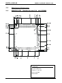
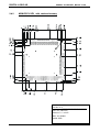
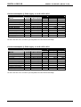
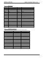
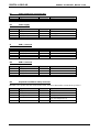
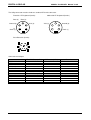
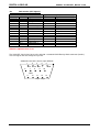
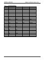
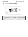
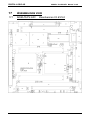
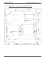
1
TECHNICAL USER'S MANUAL FOR: PC/104 plus SmartCore MSM-P5/P3 SEN / SEV MSM-P5/P3 XEN / XEV Nordstrasse 11/F CH- 4542 Luterbach Tel.: ++41 (0)32 681 58 00 Fax: ++41 (0)32 681 58 01 Email: [email protected] Homepage: http://www.digitallogic.com DIGITAL-LOGIC AG MSMP5 / P3 SEN/SEV Manual V1.6A COPYRIGHT 1998- 2003 BY DIGITAL-LOGIC AG No part of this document may be reproduced, transmitted, transcribed, stored in a retrieval system, in any form or by any means, electronic, mechanical, optical, manual, or otherwise, without the prior written permission of DIGITAL-LOGIC AG. REVISION HISTORY: Product Version MSM-Px-XEV Product Version MSM-Px-SEV V3.4 V3.5A BIOS Doc. Date/Vis: Version Version Modification: Remarks, News, Attention: V1.14 V1.14 V1.0 V1.1 12.99 FK 03.2000 STP Initial Version with TX-Chipsset New designs, updates, corrections V3.6C V2.2xc V1.2 10.2000 STP V1.1 V1.1 V1.2 V3.7c V3.7 V3.8 V2.34 V2.36 V2.37 V1.4 V1.5 V1.5A 08.2001 STP 09.2001 STP 11.2001 KUF V1.2 V3.9 V2.37 V1.6 08.2003 KUF Setup, connectors, SODIMM, new address and logo, etc P3 added, jumpers, etc New layouts, IrDA, CF, etc. ; Currents, BAT-Lifetime, Boottime New XEV Product V1.1 added Div. modifications made: - Safety regulations added - J46,J47,J50 corrected - Schematics for V3.9 added V1.2 V3.9 V2.50 V1.6A 10.2003 DAR - Mechanical dimensions added ATTENTION 1. All information in this manual and the product are subject to change without prior notice. 2. Read this manual prior installation of the product. 3. Read the security information carefully prior installtion of the product. 4. READ CHAPTER 2.10 TO UNDERSTAND THE INCOMPATIBILITIES COMPARED TO THE STANDARD PC-AT DESIGN ! Product Registration: Please register your product at: http://www.digitallogic.com -> SUPPORT -> mailservice After registration, you will receive driver & software updates, errata information, customer information and news from DIGITAL-LOGIC AG products automatically. 2 DIGITAL-LOGIC AG MSMP5 / P3 SEN/SEV Manual V1.6A Table of Contents 1 Preface ............................................................................................................................ 6 1.1 1.2 1.3 1.4 1.5 1.6 Trademarks ...................................................................................................................... 6 Disclaimer......................................................................................................................... 6 Environmental Protection Statement ............................................................................. 6 Explanation of Symbols .................................................................................................. 7 For Your Safety ................................................................................................................ 9 Limited Two Year Warranty ........................................................................................... 10 2 Overview ....................................................................................................................... 11 2.1 2.2 2.3 2.4 2.5 2.6 2.7 2.8 Standard Features ......................................................................................................... 11 Unique Features............................................................................................................. 11 MSMP5 / P3 SEV Block Diagram................................................................................. 12 MSMP5 / P3 - X/SEV specifications............................................................................. 13 Ordering codes examples ............................................................................................. 16 BIOS History................................................................................................................... 17 This product is “YEAR 2000 CAPABLE” ....................................................... 17 Mechanical Dimensions ................................................................................................ 18 2.8.1 2.8.2 MSM-P5/P3-SEV Boardversion from V3.9 with SODIMM .................................................. 18 MSM-P5/P3-XEV with soldered memory ................................................................................. 19 2.9 General view of the mechanical dimensions with PIII processor .............................. 20 2.10 MSMP5 / P3 SEV Incompatibilities to a standard PC/AT ....................................... 21 2.11 Related Application Notes ......................................................................................... 21 2.12 Thermoscan ................................................................................................................ 22 2.13 High frequency Radiation (to meet EN55022/EN61000) ........................................... 24 3 PC/104 Bus Signals..................................................................................................... 25 3.1 Expansion Bus............................................................................................................... 28 3.1.1 Addressing PCI devices on the DLAG products: ....................................................................... 28 4 Detailed System Description....................................................................................... 29 4.1 4.2 Power Requirements ..................................................................................................... 29 CPU, Boards and RAMs................................................................................................. 32 4.3 Interface.......................................................................................................................... 32 4.4 Controllers...................................................................................................................... 35 4.5 Timers and Counters ..................................................................................................... 35 4.6 BIOS................................................................................................................................ 39 4.7 CMOS RAM Map............................................................................................................. 41 4.2.1 4.2.2 4.2.3 CPUs of this MICROSPACE Product......................................................................................... 32 Numeric Coprocessor................................................................................................................. 32 DRAM Memory ........................................................................................................................... 32 4.3.1 4.3.2 4.3.3 4.3.4 4.3.5 Keyboard AT compatible and PS/2 Mouse ................................................................................ 32 Line Printer Port LPT1................................................................................................................ 32 Serial Ports COM1-COM2.......................................................................................................... 33 Floppy Disk Interface.................................................................................................................. 34 Speaker Interface ....................................................................................................................... 35 4.4.1 Interrupt Controllers.................................................................................................................... 35 4.5.1 4.5.2 4.5.3 4.5.4 Programmable Timers................................................................................................................ 35 Battery backed clock (RTC) ....................................................................................................... 36 External battery assembling: ...................................................................................................... 38 Watchdog ................................................................................................................................... 38 4.6.1 4.6.2 4.6.3 4.6.4 ROM-BIOS Sockets ................................................................................................................... 39 EEPROM Memory for Setup ...................................................................................................... 39 BIOS CMOS Setup..................................................................................................................... 40 CMOS Setup Harddisk List ........................................................................................................ 40 4.7.1 Harddisk PIO Modes .................................................................................................................. 47 3 DIGITAL-LOGIC AG 4.8 4.9 MSMP5 / P3 SEN/SEV Manual V1.6A EEPROM saved CMOS Setup........................................................................................ 48 Download the VGA-BIOS and the CORE-BIOS ........................................................... 49 4.9.1 VGA BIOS Download Function .................................................................................................. 50 4.10 Memory........................................................................................................................ 51 4.11 4.12 BIOS Data Area Definitions........................................................................................ 67 VGA, LCD .................................................................................................................... 74 4.13 4.14 4.15 4.16 HiQ Video Multimedia Support ............................................................................... 81 Video Input with the SAA7111 VIP.......................................................................... 82 Boot time..................................................................................................................... 84 Suspend / resume- time ............................................................................................. 85 4.10.1 4.10.2 4.12.1 4.12.2 4.12.3 4.12.4 4.12.5 4.12.6 4.12.7 4.12.8 System Memory Map ................................................................................................................. 51 System I/O map.......................................................................................................................... 52 VGA / LCD Controller 69000 (69030) ........................................................................................ 74 VGA / LCD BIOS for 69000 (69030) ........................................................................................ 74 Display Modes Supported .......................................................................................................... 75 VGA/LCD BIOS Support ............................................................................................................ 76 Memory 69000/69030 CRT/TFT Panels ................................................................................... 77 Memory 69000/69030 Color STN-DD Panels ........................................................................... 78 Memory 69000/69030 Mono STN-DD Panels........................................................................... 79 Video Input ................................................................................................................................. 80 5 Description of the connectors..................................................................................... 87 6 Jumper locations on the board ................................................................................. 100 6.1 6.2 6.3 The jumpers on MSMP5/P3-SEN/SEV V3.9/V3.8 ....................................................... 101 The jumpers on MSMP5/P3-SEN/SEV, since V3.7x................................................... 103 The jumpers on MSMP5/P3-XEN/SEV, since V1.1/V1.2 ............................................ 105 7 LED criterions:............................................................................................................ 107 8 Cable interface............................................................................................................ 108 8.1 8.2 8.3 8.4 8.5 The harddisk cable 44pin ............................................................................................ 108 The COM 1/2 serial interface cable ............................................................................. 109 The printer interface cable (P4)................................................................................... 110 The Micro Floppy interface cable ............................................................................... 111 Remote function........................................................................................................... 112 9 Software ...................................................................................................................... 113 9.1 9.2 The software compatibility of the MICROSPACE PC................................................. 113 Software tools and drivers for the MICROSPACE PC ............................................... 113 10 100/10 Ethernet LAN ............................................................................................... 114 10.1 Intel 82559 Ethernet chip.......................................................................................... 114 10.2 Intel 82559ER Ethernet chip..................................................................................... 116 10.3 10.4 Compact Flash (CF).................................................................................................. 117 IrDA............................................................................................................................ 117 10.1.1 10.1.2 10.1.3 10.1.4 10.1.5 10.1.6 10.2.1 10.2.2 10.2.3 10.2.4 10.2.5 10.2.6 10.4.1 10.4.2 10.4.3 Installation example for MSDOS Novell 4.11 ........................................................................... 114 Driver installation WINDOWS 95.............................................................................................. 114 Driver installation WINDOWS 98SE......................................................................................... 114 Driver installation WINDOWS NT............................................................................................. 115 Driver installation WINDOWS 2000.......................................................................................... 115 EEPROM update ...................................................................................................................... 115 Installation example for MSDOS Novell 4.11 ........................................................................... 116 Driver installation WINDOWS 95.............................................................................................. 116 Driver installation WINDOWS 98SE......................................................................................... 116 Driver installation WINDOWS NT............................................................................................. 116 Driver installation WINDOWS 2000.......................................................................................... 116 EEPROM update ...................................................................................................................... 117 BIOS Settings ........................................................................................................................... 117 Installation Windows 2000........................................................................................................ 117 Installation Windows 98 and Windows ME .............................................................................. 118 4 DIGITAL-LOGIC AG 10.4.4 MSMP5 / P3 SEN/SEV Manual V1.6A Remark for Windows ME.......................................................................................................... 118 11 Special Peripherals, Configuration......................................................................... 119 11.1 11.1.1 The Special Function Interface for MICROSPACE ................................................. 119 INT 15h SFR Functions ............................................................................................................ 119 12 Building a system..................................................................................................... 125 12.1 Starting up the system ............................................................................................. 125 13 Thermal Specifications ............................................................................................ 127 13.1 Thermal analysis for case integration..................................................................... 127 14 Diagnostics ............................................................................................................... 128 14.1 14.1.1 Failures and hints ..................................................................................................... 128 Other, so far not identified problems ........................................................................................ 128 15 Core BIOS ................................................................................................................. 129 16 Suspend-Mode / Supply........................................................................................... 129 17 Assemblings view .................................................................................................... 130 17.1 17.2 17.3 MSM-P5/P3-SEV Boardversion V3.8/V3.9............................................................ 130 MSM-P5/P3-SEV Boardversion V3.7x .................................................................... 132 MSM-P5/P3-XEV Boardversion V1.1/V1.2............................................................... 134 18 INDEX ........................................................................................................................ 136 5 DIGITAL-LOGIC AG 1 MSMP5 / P3 SEN/SEV Manual V1.6A PREFACE This document is for integrators and programmers of systems based on the MICROSPACE-Computer family. It contains information on hardware requirements, interconnections, and details of how to program the system. The specifications given in this manual were correct at the time of printing; advances mean that some may have changed in the meantime. The information contained in this document is, to the best of our knowledge, entirely correct. However, DIGITAL-LOGIC AG, cannot accept liability for any inaccuracies or the consequences thereof, of for any liability arising from the use or application of any circuit, product decribed herein, as seen fit by DIGITALLOGIC AG without further notice. 1.1 Trademarks Digtial-Logic , Digital-Logic-Logo, MICROSPACE, smartModule are registered trademarks owned worldwide by Digital-Logic AG Luterbach (Switzerland). In addition, this document may include names, company logos, and trademarks which are registered trademarks and are therefore proprietary to their respective owners. 1.2 Disclaimer DIGITAL-LOGIC AG makes no representations or warranties with respect to the contents of this manual and specifically disclaims any implied warranty of merchantability or fitness for any particular purpose. DIGITALLOGIC AG shall under no circumstances be liable for incidental or consequential damages or related expenses resulting from the use of this product, even if it has been notified of the possibility of such damage. DIGITAL-LOGIC AG reserves the right to revise this publication from time to time without obligation to notify any person of such revisions 1.3 Environmental Protection Statement This product has been manufactured to satisfy environmental protection requirements where possible. Many of the components used (structural parts, printed circuit baords, connectors, batteries, etc.) are capable of being recycled. Final disposition of this product after its service life must be accomplished in accordance with applicable country, state, or local laws or regulations. 6 DIGITAL-LOGIC AG 1.4 MSMP5 / P3 SEN/SEV Manual V1.6A Explanation of Symbols CE Conformity This symbol indicates that the product described in this manual is in compliance with all applied CE standards. Please refer also to the section “Applied Standards” in this manual. Caution, Electric Shock! This symbol and title warn of hazards due to electrical shocks (> 60V) when touching products or parts of them. Failure to observe the precautions indicated and/or prescribed by the law may endanger your life/health and/or result in damage to your material. Please refer also to the section “High Voltage Safety Instructions” on the following page. Warning, ESD Sensitive Device! This symbol and title inform that electronic boards and their components are sensitive to static electricity. Therefore, care must be taken during all handling operations and inspections of this product, in order to ensure product integrity at all times. Please read also the section “Special Handling and Unpacking Instructions” on the following page. Warning! This symbol and title emphasize points which, if not fully understood and taken into consideration by the reader, may endanger your health and/or result in damage to your material. Note... This symbol and title emphasize aspects the reader should read through carefully for his or her own advantage. 7 DIGITAL-LOGIC AG MSMP5 / P3 SEN/SEV Manual V1.6A This symbol and title warn of general hazards from mechanical, electrical, chemical failure. This may Endager your life/health and/or result in damage to your material. 8 DIGITAL-LOGIC AG 1.5 MSMP5 / P3 SEN/SEV Manual V1.6A For Your Safety Your new Digital-Logic product was developed and tested carefully to provide all features necessary to ensure its compliance with electrical safety requirements. It was also designed for a long fault-free life. However, the life expectancy of your product can be drastically reduced by improper treatment during unpacking and installation. Therefore, in the interest of your own safety and of the correct operation of your new Digital-Logic product, you are requested to conform with the following guidelines. Warning! All operations on this device must be carried out by sufficiently skilled personnel only. Caution, Electric Shock! Before installing your new Digital-Logic product, always ensure that your mains power is switched off. This applies also to the installation of piggybacks or peripherials. Serious electrical shock hazards can exist during all installation, repair and maintenance operations with this product. Therefore, always unplug the power cable and any other cables which provide external voltages before performing work. ESD Sensitive Device! Electronic boards and their components are sensitive to static electricity. Therefore, care must be taken during all handling operations and inspections of this product, in order to ensure product integrity at all times. 9 DIGITAL-LOGIC AG 1.6 MSMP5 / P3 SEN/SEV Manual V1.6A Limited Two Year Warranty DIGITAL-LOGIC AG warrants the hardware and software products it manufactures and produces to be free from defects in materials and workmanship for one year following the date of shipment from DIGITAL-LOGIC AG, Switzerland. This warranty is limited to the original purchaser of product and is not transferable. During the one year warranty period, DIGITAL-LOGIC AG will repair or replace, at its discretion, any defective product or part at no additional charge, provided that the product is returned, shipping prepaid, to DIGITAL-LOGIC AG. All replaced parts and products become property of DIGITAL-LOGIC AG. Before returning any product for repair, customers are required to contact the company. This limited warranty does not extend to any product which has been damaged as a result of accident, misuse, abuse (such as use of incorrect input voltages, wrong cabling, wrong polarity, improper or insufficient ventilation, failure to follow the operating instructions that are provided by DIGITAL-LOGIC AG or other contingencies beyond the control of DIGITAL-LOGIC AG), wrong connection, wrong information or as a result of service or modification by anyone other than DIGITAL-LOGIC AG. Neither, if the user has not enough knowledge of these technologies or has not consulted the product manual or the technical support of DIGITAL-LOGIC AG and therefore the product has been damaged. Except, as expressly set forth above, no other warranties are expressed or implied, including, but not limited to, any implied warranty of merchantability and fitness for a particular purpose, and DIGITAL-LOGIC AG expressly disclaims all warranties not stated herein. Under no circumstances will DIGITAL-LOGIC AG be liable to the purchaser or any user for any damage, including any incidental or consequential damage, expenses, lost profits, lost savings, or other damages arising out of the use or inability to use the product. 10 DIGITAL-LOGIC AG 2 OVERVIEW 2.1 Standard Features MSMP5 / P3 SEN/SEV Manual V1.6A The MICROSPACE PC/104 is a miniaturized modular device incorporating the major elements of a PC/AT compatible computer. It includes standard PC/AT compatible elements, such as: Powerful PENTIUM 166MHz up to 266MHz (including MMX support!) or PENTIUM-III (with 300 to 700MHz) BIOS ROM DRAM XEV 32 or 64 MBytes soldered SDRAM onboard SEV 32 – 256 MByte SODIMM 144pin up to 256MB 256k second level cache Timers DMA Real-time clock with CMOS-RAM and 10year battery buffer LPT1 parallel port COM1-, COM2- RS2332 serial port 16C550 comp. Speaker interface AT-keyboard interface or PS/2-keyboard interface Floppy disk interface AT-IDE harddisk interface VGA/LCD video interface PC/104 embedded BUS PS/2 mouse interface Power management functions AMP and ACPI 2 channel USB - - - 2.2 Unique Features The MICROSPACE MSMP5 / P3 SEN/SEV and XEN/XEV includes all standard PC/AT functions plus unique DIGITAL-LOGIC AG enhancements, such as: - LAN Ethernet, INTEL 82559 or 82559ER -> standard Video Input with framegrabber (optional since V3.7x) Single 5 volt supply Watchdog Power-fail EEPROM for setup and configuration Fast IrDA Compact Card holder typ 1 UL approved parts Remote Function 11 DIGITAL-LOGIC AG 2.3 MSMP5 / P3 SEN/SEV Manual V1.6A MSMP5 / P3 SEV Block Diagram CPU smartCore-P5 (TX) smartCore P3 (BX) DRAM BUS DRAM Up V3.5 (SO-DIMM up to 256MB) PCI-BUS Temp. sensor PC/104plus PCI-Signals VRAM PIIX4 Speaker RTC 2 MB LCD/VGA Controller 69000 (69030/ VRAM 4MB) EIDE D LiBAT 2x USB (since V3.8) Watchdog BIOS 256kByte EEPROM 2kByte IrDA since V3.6 Compact Card (2. IDE port since V3.6x) Super I/O 37C672 MAX2ll FD LPT1 COM1 LCD CRT MAX2ll COM2 KB Mouse 12 A 3x Video-Input PC/104 Bus Ethernet LAN INTEL 82559 or 82559ER 100/10BASE-T ISA-BUS DIGITAL-LOGIC AG 2.4 MSMP5 / P3 SEN/SEV Manual V1.6A MSMP5 / P3 - X/SEV specifications CPU: Specification CPU MSM-P5-xxx CPU MSM-P3-xxx Compatibility: 1. Level Cache: 2. Level Cache: Socket: Clock MSM-P5-xxx MSM-P3-xxx FSB Powermanagement FPU: Chipset: Nordbridge Southbridge LAN Audio Firewire IEEE1394 Video: MSM-P5-xxx MSM-P3-xxx Framegrabber/TV-Input Memory Main Memory MSM-Px- SEV/N MSM-Px- XEV/N Flash-BIOS Setup EEPROM Flash-VideoBIOS: Video RAM MSM-P5-SEV MSM-P3-SEV Video controller Controller Videomemory Channel 1 Channel 2 Bootup-Resolution 2D-Grafic 3D-Grafic Direct-X Version PnP INTEL PENTIUM-MMX INTEL PENTIUM III 8086 – Pentium 16k data and 16k code 256kByte SmartCore 320pin 166/266MHz 300 – 700MHz 66MHz Yes, AMP1.2 and ACPI Integrated Specification TX430 /BX440 from INTEL PIIX4 from INTEL 82C559 INTEL Not on board Not on board CT69000 (2Mbyte) CT69030 (4Mbyte) Philips SAA7111 (Option) Specification SDRAM, 64Bit, up to 256Mbyte in two SODIMM144 socket SDRAM, 64Bit, up to 64Mbyte direct soldered onboard 256kByte Flash 2kByte for CMOS-backup in batterless applications Serial-Flash Separate 2Mbyte Separate 4Mbyte Specification CT69000 / CT69030 2/4Mbyte CRT VGA up to 1248 x 1024 pixels TFT 640 x 480 / 800 x 600 / 1024 x 768 VGA bios depending Integrated accelerator Not available Not available Not available 13 DIGITAL-LOGIC AG External Interface Videointerfaces USB V1.1 LPT1: COM1: COM2: Keyboard: Mouse: Floppy: Harddisk: Speaker: ISA-Bus: PCI-Bus: MSMP5 / P3 SEN/SEV Manual V1.6A Specification CRT1, LCD for TFT and STN 2 channels V1.1 available Internal RS232 RS232 PS/2 PS/2 26pin FCC Interface for TEAC Minifloppy 1 channel 44pin RM2.0mm ATAIDE-cable 0.1Watt Speaker PC/104 PC/104plus Powersupply: Input voltage: Input inrush current: Protection: Spec. 3.3Volt Power Output: Power Consumption At 5V (with 32Mbyte) MSM-P5-SEV MSM-P5-SEN MSM-P3-SEV MSM-P3-SEN Standby Poweroff Physical Characteristics Dimensions: Weight: Operating Environment Relative Humidity: Nom. 5V Tolerance +/- 3% Typ. 4 Amp. , inrush current 10Amp. for powerup of 10ms. Not integrated, EMI filtered must be added external None Max. 1Amp. for LCD and Peripherals Specification typical 2.0 Amp. at 266MHz typical 1.7Amp. at 266MHz typical 2.5Amp. at 400MHz typical 2.2Amp. at 400MHz Typical 0.5 Amp. Typical 10mA Specification PC/104plus Length: Depth: Height: 170gr 91mm 99mm 25mm Specification 5 - 90% non condensing IEC68-2-30 at -20° to +50°C operating Vibration operating: Vibration nonoperating: Shock operating: Shock nonoperating: Altitude Temperature operating IEC68-2-6 10-50Hz, 0.075mm and 55-500Hz, 1.0G IEC68-2-6 10-50Hz, 0.15mm and 55-500Hz, 2.0G IEC68-2-27 10G, 11ms ½ sine IEC68-2-27 50G, 11ms, ½ sine IEC68-2-13 4571meter operating IEC68-2-1,2,14: MSM-P5-Sxx Standard -25°C to +60°C MSM-P3-Sxx Standard –25° to +50°C Extended Temp. option MIL-810-501/502 see separate table below Temperature storage IEC68-2-1,2,14: -65°C to +125°C *) *) The backupbattery is limited on –40°C to +85°C operating and storage temperature ! 14 DIGITAL-LOGIC AG Operating Temperature Extended temperature range: MSM-P5-SEV 166MHz MSM-P5-SEV 266MHz MSM-P3-SEV 300MHz MSM-P3-SEV 400MHz MSM-P3-SEV 700MHz MSM-P5-SEN MSM-P5-SEN MSM-P3-SEN MSM-P3-SEN MSM-P3-SEN 166MHz 266MHz 300MHz 400MHz 700MHz EMI / EMC Tests MSMP5 / P3 SEN/SEV Manual V1.6A Specification: MIL-810-501 MIL-810-502 -40°C -40°C -40°C -40°C -40°C to to to to to +70°C +60°C +70°C +60°C +50°C -40°C -40°C -40°C -40°C -40°C to to to to to +85°C +85°C +85°C +70°C +60°C Specification If all signals are externaly filtered and assembled into a closed metalic case ! EMC emission EN61000-6-2:2001 Conducted disturbance Radiated disturbance EMC immunity EN61000-6-2 Electrostatic discharge (ESD) Radiated RF-Field Electrical fast transients (Burst) Surge Conducted disturbances EN55022 Class B EN55022 Class B EN61000-4-2 Voltage = 4kV contact / 8kV air, Criteria A EN61000-4-3 Level = 10V/m , Criteria A EN61000-4-4 Grade 2: DC-Powerlines = 1000V (5/50ns) Grade 2: AC-Powerlines = 2000V (5/50ns) Grade 2: Signallines = 500V (5/50ns) Criteria B EN61000-4-5 Grade 2: DC-Powerlines = 1kV, (1.2/50us) Grade 2: AC-Powerlines = 2kV, (1.2/50us) Criteria B EN61000-4-6 Voltage = 10V coupled by case, Criteria A Security: e1: UL ETS 301 CE/SEV Safety Not planed Not planed Not planed Yes AR385-16 Any information is subject to change without notice. 15 DIGITAL-LOGIC AG 2.5 MSMP5 / P3 SEN/SEV Manual V1.6A Ordering codes examples With SODIMM-Holder form memory modules MSMP5SEV-166 with 0MB DRAM SODIMM ,166 MHz,VGA/LCD, LAN, -25°C to +70°C BurnIn proofed MSMP5SEV-266 with 0MB DRAM SODIMM ,266 MHz,VGA/LCD, LAN, -25°C to +70°C BurnIn proofed MSMP5SEN-266 with 0MB DRAM SODIMM ,266 MHz, no VGA, LAN, -25°C to +70°C BurnIn proofed MSMP3SEV-300 MSMP3SEV-400 MSMP3SEV-700 with 0MB DRAM SODIMM ,300 MHz,VGA/LCD, LAN, -25°C to +70°C BurnIn proofed with 0MB DRAM SODIMM ,400 MHz,VGA/LCD, LAN, -25°C to +70°C BurnIn proofed with 0MB DRAM SODIMM ,700 MHz,VGA/LCD, LAN, -25°C to +70°C BurnIn proofed MSMP3SEN-400 with 0MB DRAM SODIMM ,400 MHz,no VGA, LAN, -25°C to +70°C BurnIn proofed With onboard soldered SDRAM memories MSMP5XEV-166-32 with 32MB SDRAM, 166 MHz,VGA/LCD, LAN, -25°C to +70°C BurnIn proofed MSMP5XEV-266-64 with 64MB SDRAM, 266 MHz,VGA/LCD, LAN, -25°C to +70°C BurnIn proofed MSMP5XEN-266-64 with 64MB SDRAM, 266 MHz, no VGA, LAN, -25°C to +70°C BurnIn proofed MSMP3XEV-300-64 with 64MB SDRAM, 300 MHz,VGA/LCD, LAN, -25°C to +70°C BurnIn proofed MSMP3XEV-400-64 with 64MB SDRAM, 400 MHz,VGA/LCD, LAN, -25°C to +70°C BurnIn proofed MSMP3XEV-700-64 with 64MB SDRAM, 700 MHz,VGA/LCD, LAN, -25°C to +70°C BurnIn proofed MSMP3XEN-400-64 with 64MB SDRAM, 400 MHz,no VGA, LAN, -25°C to +70°C BurnIn proofed -E28 Extended temperature version -25°C to +85°C BurnIn proofed at 166 MHz MSMCK Cable Kit 16 DIGITAL-LOGIC AG MSMP5 / P3 SEN/SEV Manual V1.6A 2.6 BIOS History Version: 1.01 1.02 1.10 1.11 1.13 Date: Oct.98. Nov.98 May 1999 Aug 1999 Nov 1999 Status: Beta Test AMI Beta Test Beta Test Released AMI Released 1.14 Dec 2000 Released 2.20 2.3x 2.36 2.37 2.50 April 2000 May – Aug 2001 Sept.2001 Nov. 2001 Dez 2002 Released AMI Development Vers. Beta Vers. Released Phoenix 2.7 This product is “YEAR 2000 CAPABLE” Modifications: Y2K tested, EEPROM Support corrected Keyboardless booting is now working Desktop BIOS initialisation Modified for 266MHz CPU Watchdog support added. Default data for boot without battery PCI table updated Intermediate Version New BIOS Version New BIOS Version This DIGITAL-LOGIC product is “YEAR 2000 CAPABLE”. This means, that upon installation, it accurately stores, displays, processes, provides and/or receives date data from, into, and between 1999 and 2000, and the 20. and 21. centuries, including leap year calculations, provided that all other technology used in combination with said product properly exchanges date data with it. DIGITAL-LOGIC makes no representation about individual components within the product should be used independently from the product as a whole. You should understand that DIGITAL-LOGIC’s statement that an DIGITAL-LOGIC product is “YEAR 2000 CAPABLE” means only that DIGITAL-LOGIC has verified that the product as a whole meet this definition when tested as a stand-alone product in a test lab, but dies not mean that DIGITAL-LOGIC has verified that the product is “YEAR 2000 CAPABLE” as used in your particular situation or configuration. DIGITAL-LOGIC makes no representation about individual components, including software, within the product should they be used independently from the product as a whole. DIGITAL-LOGIC customers use DIGITAL-LOGIC products in countless different configurations and in conjunction with many other components ans systems, and DIGITAL-LOGIC has no way to test wheter all those configurations and systems will properly handle the transition to the year 2000. DIGITAL-LOGIC encourages its customers and others to test whether their own computer systems and products will properly handle the transition to the year 2000. The only proper method of accessing the date in systems is indirectly from the Real-Time-Clock via the BIOS. The BIOS in DIGITAL-LOGIC computerboards contain a century checking and maintenance feature the checks the laest two significant digits of the year stored in the RTC during each BIOS request (INT 1A) to read the date and, if less than ‘80’ (i.e. 1980 is the first year supported by the PC), updates the century byte to ‘20’. This feature enables operating systems and applications using BIOS date/time services to reliably manipulate the year as a four-digit value. 17 DIGITAL-LOGIC AG MSMP5 / P3 SEN/SEV Manual V1.6A 2.8 Mechanical Dimensions 2.8.1 MSM-P5/P3-SEV Boardversion from V3.9 with SODIMM MSMP5 / P3SEV Version V3.9___________________________ Unit: mm (millimeter) Tolerance: +/- 0.1mm Date: 22.10.2003 Author: BRR 18 DIGITAL-LOGIC AG 2.8.2 MSMP5 / P3 SEN/SEV Manual V1.6A MSM-P5/P3-XEV with soldered memory MSMP5 / P3XEV Version V1.2___________________________ Unit: mm (millimeter) Tolerance: +/- 0.1mm Date: 22.10.2003 Author: BRR 19 DIGITAL-LOGIC AG MSMP5 / P3 SEN/SEV Manual V1.6A 2.9 General view of the mechanical dimensions with PIII processor 20 DIGITAL-LOGIC AG 2.10 MSMP5 / P3 SEV MSMP5 / P3 SEN/SEV Manual V1.6A Incompatibilities to a standard PC/AT No incompatibilities are observed. 2.11 Related Application Notes # 80 Description High frequency Radiation (to meet EN55022) 84 Power consumption on Pentium / any other boards with attached drives (HDD, CD) SODIMM 256MB support 97 Application Notes are availble at http://www.digitallogic.com ->support, or on any Application CD from DIGITAL-LOGIC. 21 DIGITAL-LOGIC AG 2.12 MSMP5 / P3 SEN/SEV Manual V1.6A Thermoscan 22 DIGITAL-LOGIC AG MSMP5 / P3 SEN/SEV Manual V1.6A 23 DIGITAL-LOGIC AG 2.13 MSMP5 / P3 SEN/SEV Manual V1.6A High frequency Radiation (to meet EN55022/EN61000) Since the PC/104 CPU modules are very high integrated embedded computers, no peripheral lines are protected against the radiation of high frequency spectrum. To meet a typical EN55022 requirement, all peripherals, they are going outside of the computer case, must be filtered externaly. Typical signals, they must be filtered: Keyboard: Mouse: COM1/2/3/4: LPT: CRT: KBCLK, KBDATA, VCC MSCLK, MSDATA, VCC All serial signals must be filtered All parallel signals must be filtered red,blue,green, hsynch, vsynch must be filtered Typical signals, they must not be filtered, since they are internaly used: IDE: Floppy: LCD: connected to the harddisk connected to the floppy connected to the internal LCD 1. For peripheral cables: Use for all DSUB connector a filtered version. Select carefully the filter specifications. Place the filtered DSUB connector directly frontside and be sure that the shielding makes a good contact with the case. 9pin DSUB connector from AMPHENOL: FCC17E09P 25pin DSUB connector from AMPHENOL: FCC17B25P 820pF 820pF 2. For stackthrough applications: Place on each peripheral signal line, they are going outside, a serial inductivity and after the inductivity a capacitor of 100pF to 1000pF to ground. In this case, no filtered connectors are needed. Place the filter directly under or behind the onboard connector. Serial Inductivity: Ground capacitor: TDK HF50ACB321611-T 100Mhz, 500mA, 1206 Case Ceramic Capacitor with 1000pF Power supply: Use a currentcompensated dualinductor on the 5V supply SIEMENS B82721-K2362-N1 with 3.6A , 0.4mH 24 DIGITAL-LOGIC AG 3 MSMP5 / P3 SEN/SEV Manual V1.6A PC/104 BUS SIGNALS Please note, that may not all of the signals are available on this board (check chapter 5 “Description of the connectors”) AEN, output Address Enable is used to degate the microprocessor and other devices from the I/O channel to allow DMA transfers to take place. low = CPU Cycle , high = DMA Cycle BALE, output Address Latch Enable is provided by the bus controller and is used on the system board to latch valid addresses and memory decodes from the microprocessor. This signal is used so that devices on the bus can latch LA17..23. The SA0..19 address lines latched internally according to this signal. BALE is forced high during DMA cycles. /DACK[0..3, 5..7], output DMA Acknowledge 0 to 3 and 5 to 7 are used to acknowledge DMA requests (DRQO through DRQ7). They are active low. This signal indicates that the DMA operation can begin. DRQ[0..3, 5..7], input DMA Requests 0 through 3 and 5 through 7 are asynchronous channel requests used by peripheral devices and the I/O channel microprocessors to gain DMA service (or control of the system). A request is generated by bringing a DRQ line to an active level. A DRQ line must be held high until the corresponding DMA Request Acknowledge (DACK/) line goes active. DRQO through DRQ3 will perform 8-Bit DMA transfers; DRQ57 are used for 16 accesses. /IOCHCK, input IOCHCK/ provides the system board with parity (error) information about memory or devices on the I/O channel. low = parity error, high = normal operation IOCHRDY, input I/O Channel Ready is pulled low (not ready) by a memory or I/O device to lengthen I/O or memory cycles. Any slow device using this line should drive it low immediately upon detecting its valid address and a Read or Write command. Machine cycles are extended by an integral number of one clock cycle (67 nanoseconds). This signal should be held in the range of 125-15600nS. low = wait, high = normal operation /IOCS16, input I/O 16 Bit Chip Select signals the system board that the present data transfer is a 16-Bit, 1 wait-state, I/0 cycle. It is derived from an address decode. /IOCS16 is active low and should be driven with an open collector (300 ohm pull-up) or tri-state driver capable of sinking 20mA. The signal is driven based only on SA15-SAO (not /IOR or /IOW) when AEN is not asserted. In the 8 Bit I/O transfer, the default transfers a 4 wait-state cycle. /IOR, input/output I/O Read instructs an I/O device to drive its data onto the data bus. It may be driven by the system microprocessor or DMA controller, or by a microprocessor or DMA controller resident on the I/O channel. This signal is active low. /IOW, input/output I/O Write instructs an I/O device to read the data on the data bus. It may be driven by any microprocessor or DMA controller in the system. This signal is active low. 25 DIGITAL-LOGIC AG MSMP5 / P3 SEN/SEV Manual V1.6A IRQ[ 3 - 7, 9 - 12, 14, 15], input These signals are used to tell the microprocessor that an I/O device needs attention. An interrupt request is generated when an IRQ line is raised from low to high. The line must be held high until the microprocessor acknowledges the interrupt request. /Master, input This signal is used with a DRQ line to gain control of the system. A processor or DMA controller on the I/0 channel may issue a DRQ to a DMA channel in cascade mode and receive a /DACK. /MEMCS16, input MEMCS16 Chip Select signals the system board if the present data transfer is a 1 wait-state, 16-Bit, memory cycle. It must be derived from the decode of LA17 through LA23. /MEMCS16 should be driven with an open collector (300 ohm pull-up) or tri-state driver capable of sinking 2OmA. /MEMR input/output These signals instruct the memory devices to drive data onto the data bus. /MEMR is active on all memory read cycles. /MEMR may be driven by any microprocessor or DMA controller in the system. When a microprocessor on the I/0 channel wishes to drive /MEMR, it must have the address lines valid on the bus for one system clock period before driving /MEMR active. These signals are active low. /MEMW, input/output These signals instruct the memory devices to store the data present on the data bus. /MEMW is active in all memory read cycles. /MEMW may be driven by any microprocessor or DMA controller in the system. When a microprocessor on the I/O channel wishes to drive /MEMW, it must have the address lines valid on the bus for one system clock period before driving /MEMW active. Both signals are active low. OSC, output Oscillator (OSC) is a high-speed clock with a 70 nanosecond period (14.31818 MHz). This signal is not synchronous with the system clock. It has a 50% duty cycle. OSC starts 100µs after reset is inactive. RESETDRV, output Reset Drive is used to reset or initiate system logic at power-up time or during a low line-voltage outage. This signal is active high. When the signal is active all adapters should turn off or tri-state all drivers connected to the I/O channel. This signal is driven by the permanent Master. /REFRESH, input/output These signals are used to indicate a refresh cycle and can be driven by a microprocessor on the I/0 channel. These signals are active low. SAO-SA19, LA17 - LA23 input/output Address bits 0 through 19 are used to address memory and I/0 devices within the system. These 20 address lines, allow access of up to 1MBytes of memory. SAO through SA19 are gated on the system bus when BALE is high and are latched on the falling edge of BALE. LA17 to LA23 are not latched and addresses the full 16 MBytes range. These signals are generated by the microprocessors or DMA controllers. They may also be driven by other microprocessor or DMA controllers that reside on the I/0 channel. The SA17-SA23 are always LA17-LA23 address timings for use with the MSCS16 signal. This is advanced AT96 design. The timing is selectable with jumpers LAxx or SAxx. /SBHE, input/output Bus High Enable (system) indicates a transfer of data on the upper byte of the data bus, XD8 through XD15. Sixteen-Bit devices use /SBHE to condition data-bus buffers tied to XD8 through XD15. 26 DIGITAL-LOGIC AG MSMP5 / P3 SEN/SEV Manual V1.6A SD[O..15], input/output These signals provide bus bits 0 through 15 for the microprocessor, memory, and I/0 devices. DO is the least-significant Bit and D15 is the most significant Bit. All 8-Bit devices on the I/O channel should use DO through D7 for communications to the microprocessor. The 16-Bit devices will use DO through D15. To support 8-Bit device, the data on D8 through D15 will be gated to DO through D7 during 8-Bit transfers to these devices; 16-Bit microprocessor transfers to 8-Bit devices will be converted to two 8-Bit transfers. /SMEMR input/output These signals instruct the memory devices to drive data onto the data bus for the first MByte. /SMEMR is active on all memory read cycles. /SMEMR may be driven by any microprocessor or DMA controller in the system. When a microprocessor on the I/0 channel wishes to drive /SMEMR, it must have the address lines valid on the bus for one system clock period before driving /SMEMR active. The signal is active low. /SMEMW, input/output These signals instruct the memory devices to store the data present on the data bus for the first MByte. /SMEMW is active in all memory read cycles. /SMEMW may be driven by any microprocessor or DMA controller in the system. When a microprocessor on the I/O channel wishes to drive /SMEMW, it must have the address lines valid on the bus for one system clock period before driving /SMEMW active. Both signals are active low. SYSCLK, output This is a 8 MHz system clock. It is a synchronous microprocessor cycle clock with a cycle time of 167 nanoseconds. The clock has a 66% duty cycle. This signal should only be used for synchronization. TC output Terminal Count provides a pulse when the terminal count for any DMA channel is reached. The TC completes a DMA-Transfer. This signal is expected by the onboard floppy disk controller. Do not use this signal, because it is internally connected to the floppy controller. /OWS, input The Zero Wait State (/OWS) signal tells the microprocessor that it can complete the present bus cycle without inserting any additional wait cycles. In order to run a memory cycle to a 16-Bit device without wait cycles, /OWS is derived from an address decode gated with a Read or Write command. In order to run a memory cycle to an 8-Bit device with a minimum of one-wait states, /OWS should be driven active one system clock after the Read or Write command is active, gated with the address decode for the device. Memory Read and Write commands to an 8-Bit device are active on the falling edge of the system clock. /OWS is active low and should be driven with an open collector or tri-state driver capable of sinking 2OmA. 12V +/- 5% used only for the flatpanel supply. GROUND = 0V used for the entire system. VCC, +5V +/- 0.25V for logic and harddisk/floppy supply. For further Informations about PC/104 and PC/104plus, please refer to the PC/104 specification manual which is available on the internet. http://www.digitallogic.com (manuals) 27 DIGITAL-LOGIC AG 3.1 MSMP5 / P3 SEN/SEV Manual V1.6A Expansion Bus The bus currents are as follows: Output Signals: IOH: IOL: D0 - D16 A0 - A23 MR, MW, IOR, IOW, RES, ALE, AEN, C14 DACKx, DRQx, INTx, PSx, OPW 8 mA 8 mA 8 mA 8 mA 8 mA 8 mA 8 mA 8 mA Output Signals: Logic Family: Voltage: Input Signals: ABT-Logic ViH (min.) = 2.15 V ABT-Logic Vil (max.) = 0.85 V 3.1.1 Addressing PCI devices on the DLAG products: DEVICE IDSEL PIRQ PIIX4 SLOT 1 SLOT 2 SLOT 3 SLOT 4 AD18 AD20 AD21 AD22 AD23 A/B/C/D B/C/D/A C/D/A/B D/A/B/C VGA SCSI LAN PCMCIA PCI-PCI bridge ISDN AD31 AD30 AD29 AD28 AD27 AD26 B A C/D B #REG #GNT Remarks For additional cards (peripheral boards) For additional cards (peripheral boards) For additional cards (peripheral boards) For additional cards (peripheral boards) 1 0 2 3 1 1 0 2 3 1 28 Onboard devices Onboard devices Onboard devices Onboard devices Onboard devices Onboard devices DIGITAL-LOGIC AG 4 MSMP5 / P3 SEN/SEV Manual V1.6A DETAILED SYSTEM DESCRIPTION This system has a system configuration based on the ISA architecture. Check the I/O and the Memory map in this chapter. 4.1 Power Requirements The power is connected through the PC/104 power connector; or the separate power connector on the board. The supply uses only the +5 Volts and ground connection. Warning: Make sure that the power plug is wired correctly before supplying power to the board ! A built-in diode protects the board against reverse polarity. Tolerance of 5V supply: 5 volts ± 5%; Power-fail signal starts at ± 10 % of 5 volt norm and generates a reset status for the MICROSPACE PC. Testenvironment for powerconsumption measurement: Peripheries: Harddisk Hitachi Mod-DK23AA-60 DLAG: 890005 Monitor Compaq Mod-460 PS/2-KB Logitech Mod-iTouch Keyboard PS/2-MS Logitech Mod-M-CAA43 Floppy TEAC Mod-FD-05HF Software: MS-DOS V6.22 Win2000, WinME HCT for Win2000 v9.5 BM v1.033d 29 DIGITAL-LOGIC AG MSMP5 / P3 SEN/SEV Manual V1.6A Current consumption @ 5Volt supply at –30°C/+25°C/+85°C Mode Memory DLAG-Nr. MSMP5-SEV-266MHz (DLAG: 801562) DOS: C:\ 64 MB 890644 SDRAM 128 MB 890646 SDRAM 256 MB 890647 SDRAM DOS: EDIT running 64 MB 890644 SDRAM Autoexec.bat 128 MB 890646 SDRAM 256 MB 890647 SDRAM Win2000: Desktop 64 MB 890644 SDRAM 128 MB 890646 SDRAM 256 MB 890647 SDRAM Win2000: HCT v9.5 64 MB 890644 SDRAM System\Stress\SystemStress 128 MB 890646 SDRAM 256 MB 890647 SDRAM MSMP5-SEV-266MHz -30 °C [mA] 2140 2160 2440 2140 2160 2460 1290 1300 1560 2490 2450 2830 +25°C [mA] 2070 2090 2430 2090 2110 2460 1280 1290 1530 2430 2380 2810 +85 °C [mA] 1290 1300 1520 1290 1300 1520 1290 1110 1320 1460 1520 1670 At +85°C the CPU runs at a lower speed to protect the CPU from overheating ! Current consumption @ 5Volt supply at –30°C/+25°C/+85°C Mode Memory DLAG-Nr. MSMP5-SEN-266MHz (DLAG: 801567) DOS: C:\ 64 MB 890644 SDRAM 128 MB 890646 SDRAM 256 MB 890647 SDRAM DOS: EDIT running 64 MB 890644 SDRAM Autoexec.bat 128 MB 890646 SDRAM 256 MB 890647 SDRAM Win2000: Desktop 64 MB 890644 SDRAM 128 MB 890646 SDRAM 256 MB 890647 SDRAM Win2000: HCT v9.5 64 MB 890644 SDRAM System\Stress\SystemStress 128 MB 890646 SDRAM 256 MB 890647 SDRAM MSMP5-SEN-266MHz -30 °C [mA] 1910 1930 1930 1900 1950 1930 1090 1140 1120 2210 2200 2150 +25°C [mA] 1960 1980 2160 2000 2010 2191 1120 1130 1330 2560 2390 2750 At +85°C the CPU runs at a lower speed to protect the CPU from overheating ! 30 +85 °C [mA] 1130 1092 1320 1130 1090 1320 940 910 1120 2110 2010 2210 DIGITAL-LOGIC AG MSMP5 / P3 SEN/SEV Manual V1.6A Current consumption @ 5Volt supply at –30°C/+25°C/+85°C Mode Memory DLAG-Nr. MSMP3-SEV-400MHz (DLAG: 801800) DOS: C:\ 890644 SDRAM 64 MB 128 MB 890646 SDRAM 256 MB 890562 SDRAM DOS: EDIT running 890644 SDRAM 64 MB AUTOEXEC.BAT 128 MB 890646 SDRAM 256 MB 890562 SDRAM Win2000: Desktop 890644 SDRAM 64 MB 128 MB 890646 SDRAM 256 MB 890562 SDRAM Win2000: HCT v9.5 890644 SDRAM 64 MB System\Stress\Systemstress 128 MB 890646 SDRAM 256 MB 890562 SDRAM MSMP3-SEV-400MHz -30 °C [mA] 2690 2700 3040 2710 2720 3060 1530 1540 1810 3210 3230 3520 +25°C [mA] 2770 2780 3110 2790 2800 3130 1660 1650 1930 2970 3270 3420 +85 °C [mA] 1800 1810 2040 1810 1810 2040 1590 1610 1830 1980 2210 2360 At +85°C the CPU runs at a lower speed to protect the CPU from overheating ! Current consumption @ 5Volt supply at –30°C/+25°C/+85°C Mode Memory MSMP3-SEN-400C (DLAG: 801810) DOS: C:\ 64 MB 128 MB 256 MB DOS: EDIT running 64 MB Autoexec.bat 128 MB 256 MB Win2000: Desktop 64 MB 128 MB 256 MB Win2000: HCT v9.5 64 MB System\Stress\Systemstress 128 MB 256 MB MSMP3-SEN-400MHz DLAG-Nr. 890644 SDRAM 890646 SDRAM 890562 SDRAM 890644 SDRAM 890646 SDRAM 890562 SDRAM 890644 SDRAM 890646 SDRAM 890562 SDRAM 890644 SDRAM 890646 SDRAM 890647 SDRAM -25 °C [mA] 2550 2580 2890 2570 2590 2920 1410 1430 2700 3060 3080 3350 +25°C [mA] 2820 2820 3140 2840 2840 3160 1620 1410 1740 3120 3180 3270 At +85°C the CPU runs at a lower speed to protect the CPU from overheating ! 31 +85 °C [mA] 1770 1760 2030 1770 1760 2030 1920 1700 2020 3420 3470 3550 DIGITAL-LOGIC AG MSMP5 / P3 SEN/SEV Manual V1.6A 4.2 CPU, Boards and RAMs 4.2.1 CPUs of this MICROSPACE Product Processor: Type: P5-166MHz P5-266MHz 4.2.2 Clock: Intel Intel Landmark MHz: 166 MHz 266 MHz Landmark Units: 166 MHz 266 MHz 900 1500 Numeric Coprocessor Is always integrated into the Pentium CPUs. 4.2.3 Speed: Size: Bits: Capacity: Bank: DRAM Memory 70ns soldered onboard TSOP DRAMs SODIMM 144pin 32 Bit 32, 64 MBytes SODIMM (up to 256MB) 1, 2 4.3 Interface 4.3.1 Keyboard AT compatible and PS/2 Mouse 4.3.2 Pin Signal Pin 1 Pin 2 Pin 3 Pin 4 Pin 5 Pin 6 Pin 7 Pin 8 Pin 9 Pin 10 Speaker out GND Ext. reset input VCC Keyb. Data Keyb. Clock GND Ext. Battery Mouse Clock (PS/2) Mouse Data (PS/2) Line Printer Port LPT1 A standard bi-directional LPT port is integrated into the MICROSPACE PC. Further information about these signals is available in numerous publications, including the IBM technical reference manuals for the PC and AT computers and from some other reference documents. The current is: IOH = 12 mA IOL = 24mA The SMC 37C672 may be programmed via software commands. In the NEW BIOS version, this selection may be controled with the BIOS setup screen. 32 DIGITAL-LOGIC AG 4.3.3 MSMP5 / P3 SEN/SEV Manual V1.6A Serial Ports COM1-COM2 The serial channels are fully compatible with 16C550 UARTS. COM1 is the primary serial port, and is supported by the board' s ROM-BIOS as the PC-DOS ' COM1'device. The secondary serial port is COM2; it is supported as the ' COM2'device. Standard: COM 1/2: SMC 37C672: 2 x 16C550 compatible serial interfaces Serial Port Connectors COM1, COM2 Pin Signal Name 1 2 3 4 5 6 7 8 9 CD DSR RXD RTS TXD CTS DTR RI GND Function Data Carrier Detect Data Set Ready Receive Data Request To Send Transmit Data Clear to Send Data TerminalReady Ring Indicator Signal Ground in/out DB25 Pin DB9 Pin in in in out out in out in 8 6 3 4 2 5 20 22 7 1 6 2 7 3 8 4 9 5 The serial port signals are compatible with the RS232C specifications. 33 DIGITAL-LOGIC AG 4.3.4 MSMP5 / P3 SEN/SEV Manual V1.6A Floppy Disk Interface The onboard floppy disk controller and ROM-BIOS support one or two floppy disk drives in any of the standard PC-DOS and MS-DOS formats shown in the table . Supported Floppy Formats Capacity 1.2 MB 720 K 1.44 M Drive size 5-1/4" 3-1/2" 3-1/2" Tracks 80 80 80 Data rate 500 KHz 250 KHz 500 KHz DOS version 3.0 - 6.22 3.2 - 6.22 3.3 - 6.22 Floppy Interface Configuration The desired configuration of floppy drives (number and type) must be properly initialized in the board' s CMOS - configuration memory. This is generally done by using DEL or F2 at bootup time. Floppy Interface connector The table shows the pinout and signal definitions of the board' s floppy disk interface connector. It is identical in pinout to the floppy connector of a standard AT. Note that, as in a standard PC or AT, both floppy drives are jumpered to the same drive select: as the ' second'drive. The drives are uniquely selected as a result of a swapping of a group of seven wires (conductors 10-16) that must be in the cable between the two drives. The seven-wire swap goes between the computer board and drive ' A' ; the wires to drive ' B'are unswapped (or swapped a second time). The 26 pin high density (1mm pitch FCC) connector has only one drive and motor select. The onboard jumper defines the drive A: or B:. Default is always A:. Floppy Disk Interface Technology We only support CMOS drives. That means that the termination resistors are 1 Kohm. 5 1/4“-drives are not recommended (TTL interface). The 26 pin Connector: FFC/FPC 0.3mm thick 1.0mm (0.039") pitch (MOLEX 52030 Serie) Floppy Disk Interface Connector FD26: Pin 1 2 3 4 5 6 10 12 14 16 17 18 19 20 21 22 23 24 25 26 Signal Name VCC IDX VCC DS2 VCC DCHG M02 DIRC STEP WD GND WE GND TRKO GND WP GND RDD GND HS Function +5 volts Index Pulse +5 volts Drive Select 2 +5 volts Disk Change Motor On 2 Direction Select Step Write Data Signal grounds Write Enable Signal grounds Track 0 Signal grounds Write Protect Signal grounds Read Data Signal grounds Head Select 34 in/out in out in out out out out out in in in out DIGITAL-LOGIC AG 4.3.5 MSMP5 / P3 SEN/SEV Manual V1.6A Speaker Interface One of the board' s CPU device provides the logic for a PC compatible speaker port. The speaker logic signal is buffered by a transistor amplifier, and provides approximately 0.1 watt of audio power to an external 8 ohm speaker. Connect the speaker between VCC and speaker output to have no quiescient current. 4.4 Controllers 4.4.1 Interrupt Controllers An 8259A compatible interrupt controller, within the chipset, provides seven prioritized interrupt levels. Of these, several are normally associated with the board' s onboard device interfaces and controllers, and several are available on the AT expansion bus. Interrupt: - Sources: Onboard used: IRQ0 ROM-BIOS clock tick function, from timer 0 IRQ1 Keyboard controller output buffer full IRQ2 Used for cascade 2. 8259 IRQ3 COM2 serial port IRQ4 COM1 serial port IRQ5 LPT2 parallel printer (if present) IRQ6 Floppy controller IRQ7 LPT1 parallel printer IRQ8 Battery backed clock IRQ9 Free for user IRQ10 Free for user IRQ11 Free for user IRQ12 PS/2 mouse IRQ13 Math. coprocessor IRQ14 Harddisk IDE / SCSI IRQ15 Free for user * It may depends on the LAN configuration 4.5 Timers and Counters 4.5.1 Programmable Timers yes yes yes yes yes no * yes yes yes no * no * no * yes yes yes no * An 8253 compatible timer/counter device is also included in the board' s ASIC device. This device is utilized in precisely the same manner as in a standard AT implementation. Each channel of the 8253 is driven by a 1.190 MHz clock, derived from a 14.318 MHz oscillator, which can be internally divided in order to provide a variety of frequencies. Timer 2 can also be used as a general purpose timer if the speaker function is not required. Timer Assignment Timer Function 0 1 2 ROM-BIOS clock tick (18.2 Hz) DRAM refresh request timing (15 µs) Speaker tone generation time base 35 DIGITAL-LOGIC AG 4.5.2 MSMP5 / P3 SEN/SEV Manual V1.6A Battery backed clock (RTC) An AT compatible date/time clock is located within the chipset. The device also contains a CMOS static RAM, compatible with that in standard ATs. System configuration data is normally stored in the clock chip' s CMOS RAM in a manner consistent with the convention used in other AT compatible computers. Connect an external Lithium battery to J24. Make sure to use the correct polarity! The battery-backed clock can be set by using the DIGITAL-LOGIC AG SETUP at boot-time. 4.5.2.1 Battery-Lifetime of Version V3.3 - V3.7c Battery specs: Lowest temp. -40°C Manufacturer: PANASONIC Type: CR2032 Capacity versus temp. : 5µA 48mAh Voltage versus temp. : 5µA 2.9V Nominal values: 3.0V / 48mAh / -40°C...+85°C Information taken from the datasheet of PANASONIC CR2032 PRODUCT: MSMP5/3 version 3.7c Battery current: Battery-Lifetime: Nominal temp. +20°C Highest temp. +85°C 48mAh 3.0V 48mAh 3.1V Temperatur °C Battery voltage V VCC (+5V) switched ON µA VCC (+5V) Switched OFF µA +25°C -40°C +85°C 2.9 2.8 2.93 0 0 0 2.58 1.89 9.24 >10 years > 10 years 0.5 years 2.1 years 2.9 years 0.5 years +25°C -40°C +85°C 36 DIGITAL-LOGIC AG 4.5.2.2 MSMP5 / P3 SEN/SEV Manual V1.6A Bettery-Lifetime of Version V3.8 Battery specs: Lowest temp. -40°C Manufacturer: MAXELL Type: ER10/28 Capacity vers. Temp: 5uA 410mAh Voltage vers. Temp. 5uA 3.5V Nominal values: 3.6V / 410mAh / -55°C...~+85°C Information taken from the datasheet of MAXELL ER10/28 PRODUCT: MSMP5/3 version 3.8 Battery current: Battery-Lifetime: Nominal temp. +20°C Highest temp. +85°C 410mAh 3.6V 410mAh 3.8V Temperatur °C Battery voltage V VCC (+5V) switched ON µA VCC (+5V) switched off µA +25°C -40°C +85°C 3.6 3.5 3.8 0 0 0 2.8 2.0 9.8 >10 years >10 years >10 years >10 year > 10 year 4.5 year +25°C -40°C +85°C 37 DIGITAL-LOGIC AG 4.5.3 MSMP5 / P3 SEN/SEV Manual V1.6A External battery assembling: If customer wants to connect an external battery (check for the appropriate connector in the chapter DESCRIPTION OF THE CONNECTORS), then some precautions have to be made: • To prevent, that the external battery gets charged from the board, a diode has to be assembled in serial from the battery to the connector This is not necessary anymore since boardversion V3.8 (Schottky- diode included onboard) • The RTC device (PIIX4) defines a voltage level of 2.0V...3.6V, so do use an external battery, which will be in this range (inclusive the diode which is already assembled onboard since V3.8) 4.5.4 Watchdog The watchdog timer detects a system crash and performs a hardware reset. After power up, the watchdog is always disabled as the BIOS does not send strobes to the watchdog. In case that the user wants to take advantage of the watchdog, the application must produce a strobe at least every 800 ms. If no strobe occures within the 800 ms, the watchdog resets the system. To program the watchdog in user application DIGITAL-LOGIC AG has implemented a special BIOS extension in interrupt 15h (function: EBh). Calling this function by setting a 1 in the AL- Register, turns on the watchdog and performs a strobe. Calling the same function with a 0 in the AL-Register, turns off the watchdog. The following part has to be implemented in the users application: Watchdog on: The application has to call interrupt 15h function EBh and set a 1 into the AL-register at least every 800 ms. Watchdog off: The application has to call interrupt 15h function EBh and set a 0 into the AL-register within 800 ms after the last strobe has been sent while the watchdog was still in function (if the watchdog is not turned off in time, it will reset the system again!). See also chapter 11 38 DIGITAL-LOGIC AG MSMP5 / P3 SEN/SEV Manual V1.6A 4.6 BIOS 4.6.1 ROM-BIOS Sockets An EPROM socket with 8 Bit wide data access normally contains the board' s AT compatible ROM-BIOS. The socket takes a 29F020 EPROM (or equivalent) device. The board' s wait-state control logic automatically inserts four memory wait states in all CPU accesses to this socket. The ROM-BIOS sockets occupies the memory area from C0000H through FFFFFh; however, the board' s ASIC logic reserves the entire area from C0000h through FFFFFh for onboard devices, so that this area is already usable for ROM-DOS and BIOS expansion modules. Consult the appropriate address map for the MICROSPACE MSMP5SEN/SEV ROMBIOS sockets. 4.6.1.1 Standard BIOS ROM DEVICE: 29F020 PLCC32 MAP: E0000 - FFFFFh C0000 - CBFFFh CC000 - CFFFFh 4.6.2 Core BIOS 128k VGA BIOS 32k reserved EEPROM Memory for Setup The EEPROM is used for setup and configuration data, stored as an alternative to the CMOS-RTC. Optionally, the EEPROM setup driver may update the CMOS RTC, if the battery is running down and the checksum error would appear and stop the system. The capacity of the EEPROM is 2 kByte. Organisation of the 2048Byte EEPROMs: Address MAP: 0000h 0001h 0003h 0010h-007Fh 0080h-00FFh 0100h-010Fh 0110h-0113h 0114h-0117h 0118h-011Bh 011Ch-011Fh 0120h-0122h 0123h-0125h 0126h-0128h 0129h-012Bh 0130h 0131h 0132h/0133h 0134h/0135h 0136h 0137h 0200h-03FFh 0200h-027Fh 0400h-07FFh Function: CMOS-Setup valid (01=valid) Keymatrix-Setup valid (01=valid) Flag for DLAG-Message (FF=no message) Copy of CMOS-Setup data reserved for AUX-CMOS-Setup Serial-Number Production date (year/day/month) 1. Service date (year/day/month) 2. Service date (year/day/month) 3. Service date (year/day/month) Booterrors (Autoincremented if any booterror occurs) Setup Entries (Autoincremented on every Setup entry) Low Battery (Autoincremented everytime the battery is low, EEPROM -> CMOS) Startup (Autoincremented on every poweron start) Number of 512k SRAM Number of 512k Flash BIOS Version (V1.4 => [0132h]:= 4, [0133h]:=1) BOARD Version (V1.5 => [0124h]:=5, [0125h]:=1) BOARD TYPE (‘M’=PC/104, ‘E’=Euro, ‘W’=MSWS, ‘S’=Slot, ‘C’=Custom) CPU TYPE (01h=ELAN300/310, 02h=ELAN400, 03h=486SLC, 04h=486DX, 05h=P5). Keymatrix-Setup data Keymatrix Table Free for Customer’s use 39 DIGITAL-LOGIC AG 4.6.3 MSMP5 / P3 SEN/SEV Manual V1.6A BIOS CMOS Setup If wrong setups are memorized in the CMOS-RAM, the default values will be loaded after resetting the RTC/CMOS-RAM with the CMOS-RESET jumper. If the battery is down, it is always possible to start the system with the default values from the BIOS. WARNING: On the next setup pages (switch with TAB) the values for special parameters are modifiable. Normally the parameters are set correctly by DIGITAL-LOGIC AG. Be very careful in modifying any parameter since the system could crash. Some parameters are dependent on the CPU type. The cache parameter is always available, for example. So, if you select too few wait states, the system will not start until you reset the CMOS-RAM using the RAM-Reset jumper, but the default values are reloaded. If you are not familiar with these parameters, do not change anything! 4.6.4 CMOS Setup Harddisk List Use type 48 and type 49 for user defined harddisk entries. Enter the sectors, cylinders and the number of heads. Select AUTODETECT in order to autoidentify the harddisk parameters. 40 DIGITAL-LOGIC AG 4.7 MSMP5 / P3 SEN/SEV Manual V1.6A CMOS RAM Map Systems based on the industry-standard specification include a battery backed Real Time Clock chip. This clock contains at least 64 bytes of non-volatile RAM. The system BIOS uses this area to store information including system configuration and initialization parameters, system diagnostics, and the time and date. This information remains intact even when the system is powered down. The BIOS supports 128 bytes of CMOS RAM. This information is accessible through I/O ports 70h and 71h. CMOS RAM can be divided into several segments: Locations 00h - 0Fh contain real time clock (RTC) and status information Locations 10h - 2Fh contain system configuration data Locations 30h - 3Fh contain System BIOS-specific configuration data as well as chipset-specific information Locations 40h - 7Fh contain chipset-specific information as well as power management configuration parameters The following table provides a summary of how these areas may be further divided. Beginning Ending Checksum Description 00h 10h 2Eh 30h 34h 40h 5Ch 5Eh 6Fh 7Eh 0Fh 2Dh 2Fh 33h 3Fh 5Bh 5Dh 6Eh 7Dh 7Fh No Yes No No No Yes No No Yes No RTC and Checksum System Configuration Checksum Value of 10h - 2Dh Standard CMOS Standard CMOS - SystemSoft Reserved Extended CMOS - Chipset Specific Checksum Value of 40h - 5Bh Extended CMOS - Chipset Specific Extended CMOS - Power Management Checksum Value of 6Fh - 7Dh 41 DIGITAL-LOGIC AG MSMP5 / P3 SEN/SEV Manual V1.6A Location 00h Description Time of day (seconds) specified in BCD 01h Alarm (seconds) specified in BCD 02h Time of Day (minutes) specified in BCD 03h Alarm (minutes) specified in BCD 04h Time of Day (hours) specified in BCD 05h Alarm (hours) specified in BCD 06h Day of week specified in BCD 07h Day of month specified in BCD 08h Month specified in BCD 09h Year specified in BCD 0Ah Status Register A Bit 7 = Update in progress Bits 6-4 = Time based frequency divider Bits 3-0 = Rate selection bits that define the periodic interrupt rate and output frequency. 0Bh Status Register B Bit 7 = Run/Halt 0 Run 1 Halt Bit 6 = Periodic Timer 0 Disable 1 Enable Bit 5 = Alarm Interrupt 0 Disable 1 Enable Bit 4 = Update Ended Interrupt 0 Disable 1 Enable Bit 3 = Square Wave Interrupt 0 Disable 1 Enable Bit 2 = Calendar Format 0 BCD 1 Binary Bit 1 = Time Format 0 12-Hour 1 24-Hour Bit 0 = Daylight Savings Time 0 Disable 1 Enable 0Ch Status Register C Bit 7 = Interrupt Flag Bit 6 = Periodic Interrupt Flag Bit 5 = Alarm Interrupt Flag Bit 4 = Update Interrupt Flag Bits 3-0 = Reserved 0Dh Status Register D Bit 7 = Real Time Clock 0 Lost Power 1 Power Continued... 42 DIGITAL-LOGIC AG CMOS Map MSMP5 / P3 SEN/SEV Manual V1.6A Continued... Location Description 0Eh CMOS Location for Bad CMOS and Checksum Flags bit 7 = Flag for CMOS Lost Power 0 1 bit 6 = = Power OK Lost Power = Flag for CMOS checksum bad 0 1 = = 0Fh Shutdown Code 10h Diskette Drives bits 7-4 = Diskette Drive A 0000 0001 0010 0011 0100 0101 = = = = = = Checksum is valid Checksum is bad Not installed Drive A = 360 K Drive A = 1.2 MB Drive A = 720 K Drive A = 1.44 MB Drive A = 2.88 MB bits 3-0 = Diskette Drive B 0000 0001 0010 0011 0100 0101 = = = = = = Not installed Drive B = 360 K Drive B = 1.2 MB Drive B = 720 K Drive B = 1.44 MB Drive B = 2.88 MB 11h Reserved 12h Fixed (Hard) Drives bits 7-4 = Hard Drive 0, AT Type 0000 = 0001-1110 1111 = Not installed Types 1 - 14 Extended drive types 16-44. See location 19h. bits 3-0 = Hard Drive 1, AT Type 0000 = 0001-1110 1111 = Not installed Types 1 - 14 Extended drive types 16-44. location 2Ah. See See the Fixed Drive Type Parameters Table in Chapter 2 for information on drive types 16-44. 13h Reserved Continued... 43 DIGITAL-LOGIC AG CMOS Map MSMP5 / P3 SEN/SEV Manual V1.6A Continued... Location Description 14h Equipment bits 7-6 = Number of Diskette Drives 00 = 01 = 10, 11 = One diskette drive Two diskette drives Reserved bits 5-4 = Primary Display Type 00 01 10 11 = = = = Adapter with option ROM CGA in 40 column mode CGA in 80 column mode Monochrome bits 3-2 = Reserved bit 1 = Math Coprocessor Presence 0 1 bit 0 = = = Bootable Diskette Drive 0 1 = = Not installed Installed Not installed Installed 15h Base Memory Size (in KB) - Low Byte 16h Base Memory Size (in KB) - High Byte 17h Extended Memory Size in (KB) - Low Byte 18h Extended Memory Size (in KB) - High Byte 19h Extended Drive Type - Hard Drive 0 See the Fixed Drive Type Parameters Table in Chapter 2 for information on drive types 16-44. 1Ah Extended Drive Type - Hard Drive 1 See the Fixed Drive Type Parameters Table in Chapter 2 for information on drive types 16-44. 1Bh Custom and Fixed (Hard) Drive Flags bits 7-6 = Reserved bit 5 = Internal Floppy Diskette Controller 0 1 bit 4 = = Disabled Enabled = Internal IDE Controller 0 1 = = Disabled Enabled bit 3 = Hard Drive 0 Custom Flag bit 2 = Hard Drive 0 IDE Flag 0 1 0 1 = = = = Disable Enabled Disable Enabled bit 1 = Hard Drive 1 Custom Flag bit 0 = Hard Drive 1 IDE Flag 0 1 0 1 = = = = Disable Enabled Disable Enabled Continued... 44 DIGITAL-LOGIC AG CMOS Map MSMP5 / P3 SEN/SEV Manual V1.6A Continued... Location Description 1Ch Reserved 1Dh EMS Memory Size Low Byte 1Eh EMS Memory Size High Byte 1Fh - 24h Custom Drive Table 0 These 6 bytes (48 bits) contain the following data: Cylinders Landing Zone Write Precomp Heads Sectors/Track 10 bits 10 bits 08 bits 1Fh Byte 0 bits 7-0 = Lower 8 Bits of Cylinders 20h Byte 1 bits 7-2 = Lower 6 Bits of Landing Zone bits 1-0 = Upper 2 Bits of Cylinders 21h Byte 2 bits 7-4 = Lower 4 Bits of Write Precompensation bits 3-0 = Upper 4 Bits of Landing Zone 22h Byte 3 bits 7-6 = Reserved bits 5-0 = Upper 6 Bits of Write Precompensation 23h Byte 4 bits 7-0 = Number of Heads 24h Byte 5 bits 7-0 = Sectors Per Track 25h - 2Ah Custom Drive Table 1 These 6 bytes (48 bits) contain the following data: Cylinders Landing Zone Write Precomp Heads Sectors/Track 10 bits 10 bits 08 bits 25h Byte 0 bits 7-0 = Lower 8 Bits of Cylinders 26h Byte 1 bits 7-2 = Lower 6 Bits of Landing Zone bits 1-0 = Upper 2 Bits of Cylinders 27h Byte 2 bits 7-4 = Lower 4 Bits of Write Precompensation bits 3-0 = Upper 4 Bits of Landing Zone Continued... 45 DIGITAL-LOGIC AG CMOS Map MSMP5 / P3 SEN/SEV Manual V1.6A Continued... Location Description 28h Byte 3 bits 7-6 = Reserved bits 5-0 = Upper 6 Bits of Write Precompensation 29h Byte 4 bits 7-0 = Number of Heads 2Ah Byte 5 bits 7-0 = Sectors Per Track 2Bh Boot Password bit 7 = Enable/Disable Password 0 1 = = Disable Password Enable Password bits 6-0 = Calculated Password 2Ch SCU Password bit 7 = Enable/Disable Password 0 1 = = Disable Password Enable Password bits 6-0 = Calculated Password 2Dh Reserved 2Eh High Byte of Checksum - Locations 10h to 2Dh 2Fh Low Byte of Checksum - Locations 10h to 2Dh 30h Extended RAM (KB) detected by POST - Low Byte 31h Extended RAM (KB) detected by POST - High Byte 32h BCD Value for Century 33h Base Memory Installed bit 7 = Flag for Memory Size 0 1 = = 640KB 512KB bits 6-0 = Reserved 34h Minor CPU Revision Differentiates CPUs within a CPU type (i.e., 486SX vs 486 DX, vs 486 DX/2). This is crucial for correctly determining CPU input clock frequency. During a power on reset, Reg DL holds minor CPU revision. 35h Major CPU Revision Differentiates between different CPUs (i.e., 386, 486, Pentium). This is crucial for correctly determining CPU input clock frequency. During a power on reset, Reg DH holds major CPU revision. 36h Hotkey Usage bits 7-6 = Reserved bit 5 = Semaphore for Completed POST bit 4 = Semaphore for 0 Volt POST (not currently used) bit 3 = Semaphore for already in SCU menu bit 2 = Semaphore for already in PM menu bit 1 = Semaphore for SCU menu call pending bit 0 = Semaphore for PM menu call pending 40h-7Fh Definitions for these locations vary depending on the chipset. 46 DIGITAL-LOGIC AG 4.7.1 MSMP5 / P3 SEN/SEV Manual V1.6A Harddisk PIO Modes Block Mode Transfer: (Multi-Sector) Block mode boots IDE drive performance by increasing the amount of data transferred. No Block Mode: Block Mode: 512 Byte per interrupt up to 64 kByte per interrupt LBA (logical block addressing) is a new method of addressing data on a disk drive. In the standard ST506 (MFM) ISA hard disk, data is accessed via a cylinder - head - sector format. LBA Mode: LBA Mode disabled: max. 528 MByte per Disk LBA Mode enabled: max. 8 Gbyte per Disk Attention: The BIOS enables the LBA Mode only, if the harddisk was formatted on a system with enabled LBA. If the drive (capacity > 528MB) is formatted on a system with disabled LBA, the Core BIOS will never enable the LBA mode ! The maximum parameters are: 1024 Cyl., 16 heads, 63 Sec/Track 32Bit Transfer: Advanced PIO Modes: Warning: Some operating system can handle two 16Bit word as one 32Bit access. This accelerates the IDE transfer. IDE IDE EIDE EIDE EIDE EIDE PIO-Mode: 0 1 2 3 4 DMA 1 Timing: 600ns 383ns 240ns 180ns 120ns 160ns Transferspeed: 2 MByte/sec 5.5MByte/sec 8.3MByte/sec 11,3MByte/sec 16,6MByte/sec 13,3MByte/sec Remarks: Slowest I/O Standard I/O Fast I/O, Mem. IORDY Protocol IORDY Protocol DRQ, ATA-2 Always begin with the PIO-Mode 0 in the manual mode (not autodetect) to test a new drive or if you have troubles in the automatic mode. The autodetect mode of some drives select wrong PIO modes. 47 DIGITAL-LOGIC AG 4.8 MSMP5 / P3 SEN/SEV Manual V1.6A EEPROM saved CMOS Setup The EEPROM has different functions, as listed below: • Backup of the CMOS-Setup values. • Storing system informations like: version, production date, customisation of the board, CPU type. • Storing user/application values. The EEPROM will be updated automatically after exiting the BIOS setup menu. The system will operate also without any CMOS battery. While booting up, the CMOS is automatically updated with the EEPROM values. Press the Esc-key while powering on the system before the video shows the BIOS message and the CMOS will not be updated. This would be helpful, if wrong parameters are stored in the EEPROM and the setup of the BIOS does not start. If the system hangs or a problem appears, the following steps must be performed: 1. Reset the CMOS-Setup (use the jumper to reset or disconnect the battery for at least 10 minutes). 2. Press Esc until the system starts up. 3. Enter the BIOS Setup: a) load DEFAULT values b) enter the settings for the environment c) exit the setup 4. Restart the system. • The user may access the EEPROM through the INT15 special functions. Refer to the chapter SFI functions. • The system information are read onyl information. To read, use the SFI functions. 48 DIGITAL-LOGIC AG 4.9 MSMP5 / P3 SEN/SEV Manual V1.6A Download the VGA-BIOS and the CORE-BIOS Before downloading a BIOS, please check as follows: - Select the SHADOW option in the BIOS, for a BIOS and VGA (if this option is available). Disable the EMM386 or other memory managers in the CONFIG.SYS of your bootdisk. Make sure, that the DOWN_xxx.EXE programm and the BIOS to download are on the same path and directory! Boot the DOS without config.sys & autoexec.bat -> press “F5” while starting DOS boot. Is the empty diskspace, where the down.exe is located, larger than 64kB (for safe storage) Is the floppydisk not write-protected Start the DOWNLOADING Tool with: - Start the corresponding download tool. Refer to the table to see which tool fits in, each productgroup has its own download tool. Do never use the wrong one! Product: BIOS-Core download File-Extension: *.COR BIOS Size: Addressrange: MSM-P5S MSM-P5SV / SEV AMI- BIOS MSM-P5/P3SN / SEN AMI- BIOS MSM-P5S / MSM-P3xxx MSM-P5SV / SEV PHOENIX- BIOS MSM-P5SN / SEN / MSM-P3xxx PHOENIX- BIOS VGA-BIOS download BIOS-Ext. download 128k E0000 - FFFFFh *.V40 , *.V45 *.V48 depending on the product 32k C0000 – C7FFFh *.BIN 32k C8000 - CFFFFh AMI82602.EXE DOWN_000.EXE - AMI82602.EXE - - PHLASH.EXE PLATFORM.BIN DOWN_000.EXE DOWN_030.EXE (69030) *** - PHLASH.EXE PLATFORM.BIN - - Remarks: ** Core- file has to be renamed as written in brackets *** If downloading with DOWN_030.EXE, disable first in BIOS /Memory Cache/Cache Video Bios Area 49 DIGITAL-LOGIC AG 4.9.1 MSMP5 / P3 SEN/SEV Manual V1.6A VGA BIOS Download Function The BIOS for the VGA must be downloaded, before a LCD is connected. This could be also a new LCD- display, which needs a corresponding VGA- BIOS. How to download a VGA- BIOS: 1. 2. 3. 4. 5. 6. 7. 8. 9. 10. Restart the system with the SHADOW enabled (if available) and no EMM386 loaded. Check, if you find the DOWN_xxx.EXE and the *.V40 / *.000 files on your disk, to get downloaded. Refer to the VGABIOS.DOC for more information about the VGABIOS files. Insert the floppydisk with the program DOWN_xxx.EXE and all VGA-Drivers. Start DOWN_xxx.EXE. Check, if the DOWN program has identified the product and the shadow correctly. Select the function PROGRAMM VGA- BIOS. Select the VGA- BIOS out of the proposed file list (UP/DOWN arrows) and press ENTER. Check, if the new VGA- header is displayed on the VGA- INFO- screen. After proceeding, switch off the power and restart the board (cold start). If the download does not work: Check, if no EMM386 is loaded. Check, if no peripheral card is in the system, which occupies the same memory range. Disconnect this card. If the download is stopped or not completed, make only a warm boot and repeat the steps or download another file. As the video is may shadowed, everything is visible and a cold boot would clear the screen and nothing would be visible afterwards. If the screen flickers or is misaligned after reboot: The previously loaded VGA- BIOS is not corresponding 100% or works only on the LCD properly. - If the screen is dark after the reboot of the system: A new system BIOS must be programmed. Ask DIGITAL-LOGIC AG for the binary file. If the previous version is still programmed: Switch off the board and do not make a warm boot due to the fact that the data may are still in the shadow stored. - 50 DIGITAL-LOGIC AG MSMP5 / P3 SEN/SEV Manual V1.6A 4.10 Memory 4.10.1 System Memory Map The PENTIUM -100 CPU used as central processing unit on the MICROSPACE has a memory address space which is defined by 32 address bits. Therefore, it can address 1 GByte of memory. The memory address MAP is as follows: CPU Pentium Address: Size: Function / Comments: 000000 - 09FFFFh 0A0000 - 0BFFFFh 0C0000 - 0CBFFFh 0CC000 - 0CFFFFh 0D0000 - 0D4000h 0D4000 - 0D8000h 0D8000 - 0DFFFFh 0E0000 - 0EFFFFh 0F0000 - 0FFFFFh 100000 - 1FFFFFh 200000 - FFFFFFh 640 KBytes 128 KBytes 48 KBytes 16 KBytes 16 KBytes 16 KBytes 32 KBytes 64 KBytes 64 KBytes 1 MByte 14 MBytes Onboard DRAM for DOS applications CGA, EGA, LCD Video RAM 128kB VGA BIOS selected by the hardware BIOS extensions selected by the hardware free for user free for user free for user Core BIOS selected by the PIIX4 chipset Core BIOS selected by the PIIX4 chipset DRAM for extended onboard memory DRAM for extended onboard memory The possible system memory sizes (DRAM) are: 32 MB 64 MB MSMP5SEN/SEV-xxx-32M MSMP5SEN/SEV-xxx-64M 32 MB Memory 64 MB Memory 0 MB MSMP5 / 3P SEN/SEV-xxx-0M SODIMM 144pin 51 DIGITAL-LOGIC AG 4.10.2 MSMP5 / P3 SEN/SEV Manual V1.6A System I/O map The following table shows the detailed listing of the I/O port assignments used in the MICROSPACE board: I/O Address Read/Write Status Description 0000h R/W DMA channel 0 address byte 0 (low), then byte 1 0001h R/W DMA channel 0 word count byte 0 (low), then byte 1 0002h R/W DMA channel 1 address byte 0 (low), then byte 1 0003h R/W DMA channel 1 word count byte 0 (low), then byte 1 0004h R/W DMA channel 2 address byte 0 (low), then byte 1 0005h R/W DMA channel 2 word count byte 0 (low), then byte 1 0006h R/W DMA channel 3 address byte 0 (low), then byte 1 0007h R/W DMA channel 3 word count byte 0 (low), then byte 1 0008h R DMA channel 0-3 status register bit 7 = 1 Channel 3 request bit 6 = 1 Channel 2 request bit 5 = 1 Channel 1 request bit 4 = 1 Channel 0 request bit 3 = 1 Terminal count on channel 3 bit 2 = 1 Terminal count on channel 2 bit 1 = 1 Terminal count on channel 1 bit 0 = 1 Terminal count on channel 0 Continued... 52 DIGITAL-LOGIC AG MSMP5 / P3 SEN/SEV Manual V1.6A I/O Address Read/Write Status Description 0008h W DMA channel 0-3 command register bit 7 = DACK sense active high/low 0 low 1 high bit 6 = DREQ sense active high/low 0 low 1 high bit 5 = Write selection 0 Late write selection 1 Extended write selection bit 4 = Priority 0 Fixed 1 Rotating bit 3 = Timing 0 Normal 1 Rotating bit 2 = Controller enable/disable 0 Enable 1 Disable bit 1 = Memory-to-memory enable/disable 0 Disable 1 Enable bit 0 = Reserved 0009h W DMA write request register 000Ah R/W DMA channel 0-3 mask register bits 7-3 = Reserved bit 2 = 0 Clear bit 1 Set bit bits 1-0 = Channel Select 00 Channel 0 01 Channel 1 10 Channel 2 11 Channel 3 00Bh W DMA channel 0-3 mode register bits 7-6 = 00 Demand mode 01 Single mode 10 Block mode 11 Cascade mode bit 5 = 0 Address increment select 1 Address decrement select bit 4 = 0 Disable auto initialization 1 Enable auto initialization bits 3-2 = Operation type 00 Verify operation 01 Write to memory 10 Read from memory 11 Reserved bits 1-0 = Channel select 00 Channel 0 01 Channel 1 10 Channel 2 11 Channel 3 53 Continued... DIGITAL-LOGIC AG MSMP5 / P3 SEN/SEV Manual V1.6A I/O Address Read/Write Status Description 000Ch W DMA clear byte pointer flip/flop 000Dh R DMA read temporary register 000Dh W DMA master clear 000Eh W DMA clear mask register 000Fh W DMA write mask register 0020h W Programmable Interrupt Controller - Initialization Command Word 1 (ICW1) provided bit 4 = 1 bits 7-5 = 000 Used only in 8080 or 8085 mode bit 4 = 1 ICW1 is used bit 3 = 0 Edge triggered mode 1 Level triggered mode bit 2 = 0 Successive interrupt vectors separated by 8 bytes 1 Successive interrupt vectors separated by 4 bytes bit 1 = 0 Cascade mode 1 Single mode bit 0 = 0 ICW4 not needed 1 ICW4 needed 0021h W Used for ICW2, ICW3, or ICW4 in sequential order afterICW1 is written to port 0020h ICW2 bits 7-3 = Address A0-A3 of base vector address for interrupt controller bits 2-0 = Reserved (should be 000) ICW3 (for slave controller 00A1h) bits 7-3 = Reserved (should be 0000) bits 2-0 = 1 Slave ID ICW4 bits 7-5 = Reserved (should be 000) bit 4 = 0 No special fully nested mode 1 Special fully nested mode bits 3-2 = Mode 00 Non buffered mode 01 Non buffered mode 10 Buffered mode/slave 11 Buffered mode/master bit 1 = 0 Normal EOI 1 Auto EOI bit 0 = 0 8085 mode 1 8080 / 8088 mode Continued... 54 DIGITAL-LOGIC AG MSMP5 / P3 SEN/SEV Manual V1.6A I/O Address Read/Write Status Description 0021h R/W PIC master interrupt mask register (OCW1) bit 7 = 0 Enable parallel printer interrupt bit 6 = 0 Enable diskette interrupt bit 5 = 0 Enable hard disk interrupt bit 4 = 0 Enable serial port 1 interrupt bit 3 = 0 Enable serial port 2 interrupt bit 2 = 0 Enable video interrupt bit 1 = 0 Enable kybd/pointing device/RTC interrupt bit 0 = 0 Enable interrupt timer 0021h W PIC OWC2 (if bits 4-3 = 0) bit 7 = Reserved bits 6-5 = 000 Rotate in automatic EOI mode (clear) 001 Nonspecific EOI 010 No operation 011 Specific EOI 100 Rotate in automatic EOI mode (set) 101 Rotate on nonspecific EOI command 110 Set priority command 111 Rotate on specific EOI command bits 4-3 = Reserved (should be 00) bits 2-0 = Interrupt request to which the command applies 0020h R PIC interrupt request and in-service registers programmed by OCW3 Interrupt request register bits 7-0 = 0 No active request for the corresponding interrupt line 1 Active request for the corresponding interrupt line Interrupt in-service register bits 7-0 = 0 Corresponding interrupt line not currently being serviced 1 Corresponding interrupt line is currently being serviced 0021h W PIC OCW3 (if bit 4 = 0, bit 3 = 1) bit 7 = Reserved (should 0) bits 6-5 = 00 No operation 01 No operation 10 Reset special mask 11 Set special mask bit 4 = Reserved (should be 0) bit = Reserved (should be 1) bit 2 = 0 No poll command 1 Poll command bits 1-0 = 00 No operation 01 Operation 10 Read interrupt request register on next read at port 0020 h 11 Read interrupt in-service register on next read at port 0020h Continued... 55 DIGITAL-LOGIC AG MSMP5 / P3 SEN/SEV Manual V1.6A I/O Address Read/Write Status Description 0022h R/W Chipsset Register Address 0023h R/W Chipsset Register Data 0040h R/W Programmable Interrupt Time read/write counter 0, keyboard controller channel 0 0041h R/W Programmer Interrupt Timer channel 1 0042h R/W Programmable Interrupt Timer miscellaneous register channel 2 0043h W Programmable Interrupt Timer mode port - control word register for counters 0 and 2 bits 7-0 = Counter select 00 Counter 0 select 01 Counter 1 select 10 Counter 2 select bits 5-4 = 00 Counter latch command 01 R / W counter, bits 0-7 only 10 R / W counter, bits 8-15 only 11 R / W counter, bits 0-7 first, then bits 8-15 bits 3-1 = Select mode 000 Mode 0 001 Mode 1 programmable one shot x10 Mode 2 rate generator x11 Mode 3 square wave generator 100 Mode 4 software-triggered strobe 101 Mode 5 hardware-triggered strobe bit 0 = 0 Binary counter is 16 bits 1 Binary counter decimal (BCD) counter 0048h R/W Programmable interrupt timer 0060h R Keyboard controller data port or keyboard input buffer 0060h W Keyboard or keyboard controller data output buffer Continued... 56 DIGITAL-LOGIC AG MSMP5 / P3 SEN/SEV Manual V1.6A I/O Address Read/Write Status Description 0064h R Keyboard controller read status bit 7 = 0 No parity error 1 Parity error on keyboard transmission bit 6 = 0 No timeout 1 Received timeout bit 5 = 0 No timeout 1 Keyboard transmission timeout bit 4 = 0 Keyboard inhibited 1 Keyboard not inhibited bit 3 = 0 Data 1 Command bit 2 = System flag status bit 1 = 0 Input buffer empty 1 Input buffer full bit 0 = 0 Output buffer empty 1 Output buffer full 0064h W Keyboard controller input buffer 0070h R CMOS RAM index register port and NMI mask bit 7 = 1 NMI disabled bits 6-0 = 0 CMOS RAM index 0071h R/W CMOS RAM data register port 0080h R/W Temporary storage for additional page register 0080h R 0081h R/W DMA channel 2 address byte 2 0082h R/W DMA channel 2 address byte 2 0083h R/W DMA channel 1 address byte 2 0084h R/W Extra DMA page register 0085h R/W Extra DMA page register 0086h R/W Extra DMA page register 0087h R/W DMA channel 0 address byte 2 0088h R/W Extra DMA page register 0089h R/W DMA channel 6 address byte 2 008Ah R/W DMA channel 7 address byte 2 008Bh R/W DMA channel 5 address byte 2 008Ch R/W Extra DMA page register 008Dh R/W Extra DMA page register 008Eh R/W Extra DMA page register 008Fh R/W DMA refresh page register Manufacturing diagnostic port (this port can access POST checkpoints) Continued... 57 DIGITAL-LOGIC AG I/O Address Read/Write Status MSMP5 / P3 SEN/SEV Manual V1.6A Description 00A0h - 00A1h are reserved for the slave programmable interrupt controller. The bit definitions are identical to those of addresses 0020h - 0021h except where indicated. 00A0h R/W Programmable interrupt controller 2 00A1h R/W Programmable interrupt controller 2 mask bit 7 = 0 Reserved bit 6 = 0 Enable hard disk interrupt bit 5 = 0 Enable coprocessor execution interrupt bit 4 = 0 Enable mouse interrupt bits 3-2 = 0 Reserved bit 1 = 0 Enable redirect cascade bit 0 = 0 Enable real time clock interrupt 00C0h R/W DMA channel 4 memory address bytes 1 and 0 (low) 00C2h R/W DMA channel 4 transfer count bytes 1 and 0 (low) 00C4h R/W DMA channel 5 memory address bytes 1 and 0 (low) 00C6h R/W DMA channel 5 transfer count bytes 1 and 0 (low) 00C8h R/W DMA channel 6 memory address bytes 1 and 0 (low) 00CAh R/W DMA channel 6 transfer count bytes 1 and 0 (low) 00CCh R/W DMA channel 7 memory address bytes 1 and 0 (low) 00CEh R/W DMA channel 7 transfer count bytes 1 and 0 (low) 00D0h R Status register for DMA channels 4-7 bit 7 = 1 Channel 7 request bit 6 = 1 Channel 6 request bit 5 = 1 Channel 5 request bit 4 = 1 Channel 4 request bit 3 = 1 Terminal count on channel 7 bit 2 = 1 Terminal count on channel 6 bit 1 = 1 Terminal count on channel 5 bit 0 = 1 Terminal count on channel 4 00D0h W Command register for DMA channels 4-7 bit 7 = 0 DACK sense active low 1 DACK sense active high bit 6 = 0 DREQ sense active low 1 DREQ sense active high bit 5 = 0 Late write selection 1 Extended write selection bit 4 = 0 Fixed Priority 1 Rotating Priority bit 3 = 0 Normal Timing 1 Rotating Timing bit 2 = 0 Enable controller 1 Disable controller bit 1 = 0 Disable memory-to-memory transfer 1 Enable memory-to-memory transfer bit 0 = Reserved Continued... 58 DIGITAL-LOGIC AG MSMP5 / P3 SEN/SEV Manual V1.6A I/O Address Read/Write Status Description 00D2h W Write request register for DMA channels 4-7 00D4h W Write single mask register bit for DMA channels 4-7 bits 7-3 = 0 Reserved bit 2 = 0 Clear mask bit, 1 Set mask bit bits 1-0 = Channel select 00 Channel 4 01 Channel 5 10 Channel 6 11 Channel 7 00D6h W Mode register for DMA channels 4-7 bits 7-6 = 00 Demand mode 01 Single mode 10 Block mode 11 Cascade mode bit 5 = 0 Address increment select 1 Address decrement select bit 4 = 0 Disable auto initialization 1 Enable auto initialization bits 3-2 = Operation type 00 Verify operation 01 Write to memory 10 Read from memory 11 Reserved bits 1-0 = Channel select 00 Channel 4 01 Channel 5 10 Channel 6 11 Channel 7 00D8h W Clear byte pointer flip/flop for DMA channels 4-7 00DAh R Read Temporary Register for DMA channels 4-7 00DAh W Master Clear for DMA channels 4-7 00DCh W Clear mask register for DMA channels 4-7 00DEh W Write mask register for DMA channels 4-7 00F0h W Math coprocessor clear busy latch 00F1h W Math coprocessor reset 00F2h 00FFh R/W Math coprocessor 0140h – R/W SCSI Controller if installed 014Fh I/O addresses 0170h - 0177h are reserved for use with a secondary hard drive. See addresses 01F0h - 01F7h for bit definitions. 0170h R/W Data register for hard drive 1 0171h R Error register for hard drive 1 0171h W Precomposition register for hard drive 1 0172h R/W Sector count - hard drive 1 Continued... 59 DIGITAL-LOGIC AG MSMP5 / P3 SEN/SEV Manual V1.6A I/O Address Read/Write Status Description 0173h R/W Sector number for hard disk 1 0174h R/W Number of cylinders (low byte) for hard drive 1 0175h R/W Number of cylinders (high byte) for hard drive 1 0716h R/W Drive/head register for hard drive 1 0177h R Status register for hard drive 1 0177h W Command register for hard drive 1 01F0h R/W Data register base port for hard drive 0 01F1h R Error register for hard drive 0 Diagnostic mode bits 7-3 = Reserved bits 2-0 = Errors 0001 No errors 0010 Controller error 0011 Sector buffer error 0100 ECC device error 0101 Control processor error Operation mode bit 7 = Block 0 Bad block 1 Block not bad bit 6 = Error 0 No error 1 Uncorrectable ECC error bit 5 = Reserved bit 4 = ID 0 ID located 1 ID not located bit 3 = Reserved bit 2 = Command 0 Completed 1 Not completed bit 1 = Track 000 0 Not found 1 Found bit 0 = DRAM 0 Not found 1 Found (CP-3022 always 0) 01F1h W Write precomposition register for hard drive 0 01F2h R/W Sector count for hard disk 0 01F3h R/W Sector number for hard drive 0 01F4h R/W Number of cylinders (low byte) for hard drive 0 01F5h R/W Number of cylinders (high byte) for hard drive 0 Continued... 60 DIGITAL-LOGIC AG MSMP5 / P3 SEN/SEV Manual V1.6A I/O Address Read/Write Status Description 01F6h R/W Drive/Head register for hard drive 0 bit 7 = 1 bit 6 = 0 bit 5 = 1 bit 4 = Drive select 0 First hard drive 1 Second hard drive bits 3-0 = Head select bits 01F7h R Status register for hard drive 0 bit 7 = 1 Controller is executing a command bit 6 = 1 Drive is ready bit 5 = 1 Write fault bit 4 = 1 Seek operation complete bit 3 = 1 Sector buffer requires servicing bit 2 = 1 Disk data read completed successfully bit 1 = Index (is set to 1 at each disk revolution) bit 0 = 1 Previous command ended with error 01F7h W Command register for hard drive 0 0200h 020Fh R/W Game controller ports 0201h R/W I/O data - game port 0220h – R/W Soundport AD1816 reserved 022Fh I/O addresses 0278h - 027Ah are reserved for use with parallel port 2. See the bit definitions for addresses 0378h - 037Ah. 0278h R/W Data port for parallel port 2 0279h R Status port for parallel port 2 0279h W PnP Address register (only for PnP devices) 027Ah R/W Control port for parallel port 2 02B0h – R/W Digital I/O for Latch, WDOG, Control 02BFh I/O addresses 02E8h - 02EFh are reserved for use with serial port 4. See the bit definitions for I/O addresses 03F8h - 03FFh. 02E8h W Transmitter holding register for serial port 4 02E8h R Receive buffer register for serial port 4 02E8h R/W Baud rate divisor (low byte) when DLAB = 1 02E9h R/W Baud rate divisor ( high byte) when DLAB = 1 02E9h R/W Interrupt enable register when DLAB = 0 02EAh R Interrupt identification register for serial port 4 02EBh R/W Line control register for serial port 4 02ECh R/W Modem control register for serial port 4 02EDh R Line status register for serial port 4 02EEh R Modem status register for serial port 4 02EFh R/W Scratch register for serial port 4 (used for diagnostics) Continued... 61 DIGITAL-LOGIC AG I/O Address Read/Write Status MSMP5 / P3 SEN/SEV Manual V1.6A Description I/O addresses 02F8h - 02FFh are reserved for use with serial port 2. See the bit definitions for I/O addresses 03F8h - 03FFh. 02F8h W Transmitter holding register for serial port 2 02F8h R Receive buffer register for serial port 2 02F8h R/W Baud rate divisor (low byte) when DLAB = 1 02F9h R/W Baud rate divisor ( high byte) when DLAB = 1 02F9h R/W Interrupt enable register when DLAB = 0 02FAh R Interrupt identification register for serial port 2 02FBh R/W Line control register for serial port 2 02FCh R/W Modem control register for serial port 2 02FDh R Line status register for serial port 2 02FEh R Modem status register for serial port 2 02FFh R/W Scratch register for serial port 2 (used for diagnostics) 0300h – R/W ISA- LAN controller, if installed 031Fh (otherwise free for the user) I/O addresses 0372h - 0377h are reserved for use with a secondary diskette controller. See the bit definitions for 03F2h - 03F7h. 0372h W Digital output register for secondary diskette drive controller 0374h R Status register for secondary diskette drive controller 0375h R/W Data register for secondary diskette drive controller 0376h R/W Control register for secondary diskette drive controller 0377h R Digital input register for secondary diskette drive controller 0377h W Select register for secondary diskette data transfer rate 0378h R/W Data port for parallel port 1 0379h R Status port for parallel port 1 bit 7 = 0 Busy bit 6 = 0 Acknowledge bit 5 = 1 Out of paper bit 4 = 1 Printer is selected bit 3 = 0 Error bit 2 = 0 IRQ has occurred bit 1-0 = Reserved Continued... 62 DIGITAL-LOGIC AG MSMP5 / P3 SEN/SEV Manual V1.6A I/O Address Read/Write Status Description 037Ah R/W Control port for parallel port 1 bits 7-5 = Reserved bit 4 = 1 Enable IRQ bit 3 = 1 Select printer bit 2 = 0 Initialize printer bit 1 = 1 Automatic line feed bit 0 = 1 Strobe 03B0h 03B8h R/W Various video registers I/O addresses 03BCh - 03BEh are reserved for use with parallel port 3. See the bit definitions for addresses 0378h - 037Ah. 03BCh R/W Data port - parallel port 3 03BDh R/W Status port - parallel port 3 03BEh R/W Control port - parallel port 3 03C0h 03CFh R/W Video subsystem (EGA/VGA) 03C2h 03D9h R/W Various CGA and CRTC registers 03E0h R/W PCCARD Address select 03E1h R/W PCCARD Data transfer with 365SL controller I/O addresses 03E8h - 03EFh are reserved for use with serial port 3. See the bit definitions for I/O addresses 03F8h - 03FFh. 03E8h W Transmitter holding register for serial port 3 03E8h R Receive buffer register for serial port 3 03E8h R/W Baud rate divisor (low byte) when DLAB = 1 03E9h R/W Baud rate divisor ( high byte) when DLAB = 1 03E9h R/W Interrupt enable register when DLAB = 0 03EAh R Interrupt identification register for serial port 3 03EBh R/W Line control register for serial port 3 03ECh R/W Modem control register for serial port 3 03EDh R Line status register for serial port 3 03EEh R Modem status register for serial port 3 03EFh R/W Scratch register for serial port 3 (used for diagnostics) 03F2h W Digital output register for primary diskette drive controller bits 7-6 = 0 Reserved bit 5 = 1 Enable drive 1 motor bit 4 = 1 Enable drive 0 motor bit 3 = 1 Enable diskette DMA bit 2 = 0 Reset controller bit 1 = 0 Reserved bit 0 = 0 Select drive 0 1 Select drive 1 Continued... 63 DIGITAL-LOGIC AG MSMP5 / P3 SEN/SEV Manual V1.6A I/O Address Read/Write Status Description 03F4h R Status register for primary diskette drive controller bit 7 = 1 Data register is ready bit 6 = 0 Transfer from system to controller 1 Transfer from controller to system bit 5 = 1 Non-DMA mode bit 4 = 1 Diskette drive controller is busy bits 3-2 = Reserved bit 1 = 1 Drive 1 is busy bit 0 = 1 Drive 0 is busy 03F5h R/W Data register for primary diskette drive controller 03F6h R Control port for primary diskette drive controller bits 7-4 = Reserved bit 3 = 0 Reduce write current 1 Head select enable bit 2 = 0 Disable diskette drive reset 1 Enable diskette drive reset bit 1 = 0 Disable diskette drive initialization 1 Enable diskette drive initialization bit 0 = Reserved 03F7h R Digital input register for primary diskette drive controller bit 7 = 1 Diskette drive line change bit 6 = 1 Write gate bit 5 = Head select 3 / reduced write current bit 4 = Head select 2 bit 3 = Head select 1 bit 2 = Head select 0 bit 1 = Drive 1 select bit 0 = Drive 0 select 03F7h W Select register for primary diskette data transfer rate bits 7-2 = Reserved bits 1-0 = 00 500 Kbs mode 01 300 Kbs mode 10 250 Kbs mode 11 Reserved I/O addresses 03F8h - 03FFh are reserved for use with serial port 1. The bit definitions for these addresses also apply to serial ports 2, 3, and 4. 03F8h W Transmitter holding register for serial port 1 - Contains the character to be sent. Bit 0, the least significant bit, is the first bit sent. bits 7-0 = Data bits 0-7 when the Divisor Latch Access Bit (DLAB) is 0 03F8h R Receive buffer register for serial port 1 - Contains the character to be received. Bit 0, the least significant bit, is the first bit received. bits 7-0 = Data bits 0-7 when the Divisor Latch Access Bit (DLAB) is 0 Continued... 64 DIGITAL-LOGIC AG MSMP5 / P3 SEN/SEV Manual V1.6A I/O Address Read/Write Status Description 03F8h R/W Baud rate divisor (low byte) - This byte along with the high byte (03F9h) store the data transmission rate divisor. bits 7-0 = Data bits 0-7 when the Divisor Latch Access Bit (DLAB) is 1 03F9h R/W Baud rate divisor (high byte) - This byte along with the low byte (03F8h) store the data transmission rate divisor. bits 7-0 = Bits 8-15 when DLAB = 1 03F9h R/W Interrupt enable register bits 7-4 = Reserved bit 3 = 1 Modem status interrupt enable bit 2 = 1 Receiver line status interrupt enable bit 1 = 1 Transmitter holding register empty interrupt enable bit 0 = 1 Received data available interrupt enable when DLAB = 0 03FAh R Interrupt identification register - serial port 1 bits 7-3 = Reserved bits 2-1 = Identify interrupt with highest priority 00 Modem status interrupt (4th priority) 01 Transmitter holding register empty (3rd priority) 10 Received data available (2nd priority) 11 Receiver line status interrupt (1st priority) bit 0 = 0 Interrupt pending (register contents can be vice routine) used as a pointer to interrupt ser- 1 No interrupt pending 03FBh R/W Line control register - serial port 1 bit 7 = Divisor Latch Access (DLAB) 0 Access receiver buffer, transmitter holding register, and interrupt enable register 1 Access divisor latch bit 6 = 1 Set break enable. Forces serial output to spacing state and remains there bit 5 = Stick parity bit 4 = Even parity select bit 3 = Parity enable bit 2 = Number of stop bits bit 1 = Word length 00 5-bit word length 01 6-bit word length 10 7-bit word length 11 8-bit word length 03FCh R/W Modem control register - serial port 1 bits 7-5 = Reserved bit 4 = 1 Loopback mode for diagnostic testing of serial port. bit 3 = 1 User-defined output 2 bit 2 = 1 User-defined output 1 bit 1 = Force Request To Send active bit 0 = Force Data Terminal Ready active Continued... 65 DIGITAL-LOGIC AG MSMP5 / P3 SEN/SEV Manual V1.6A I/O Address Read/Write Status Description 03FDh R Line status register - serial port 1 bit 7 = Reserved bit 6 = 1 Transmitting shift and holding registers empty bit 5 = 1 Transmitter shift register empty bit 4 = 1 Break interrupt bit 3 = 1 Framing error bit 2 = 1 Overrun error bit 0 = 1 Data ready 03FEh R Modem status register - serial port 1 bit 7 = 1 Data Carrier Detect bit 6 = 1 Ring Indicator bit 5 = 1 Data Set Ready bit 4 = 1 Clear To Send bit 3 = 1 Delta Data Carrier bit 2 = 1 Trailing Edge Ring Indicator bit 1 = 1 Delta Data Set Ready bit 0 = 1 Delta Clear To Send 03FFh R/W Scratch register - serial port 1 (used for diagnostics) 0A79h W PnP Data write register (only for PnP devices) 66 DIGITAL-LOGIC AG 4.11 MSMP5 / P3 SEN/SEV Manual V1.6A BIOS Data Area Definitions The BIOS Data Area is an area within system RAM that contains information about the system environment. System environment information includes definitions associated with hard disks, diskette drives, keyboard, video, as well as other BIOS functions. This area is created when the system is first powered on. It occupies a 256-byte area from 0400h - 04FFh. The following table lists the contents of the BIOS data area locations in offset order starting from segment address 40:00h. Location Description 00h - 07h I/O addresses for up to 4 serial ports 08h - 0Dh I/O addresses for up to 3 parallel ports 0Eh - 0Fh Segment address of extended data address 10h - 11h Equipment list bits 15-14 = Number of parallel printer adapters 00 01 10 11 = = = = Not installed One Two Three bits 13-12 = Reserved bits 11-9 = Number of serial adapters 00 001 010 011 100 = = = = = Not installed One Two Three Four bit 8 = Reserved bits 7-6 = Number of diskette drives 00 01 = = One drive Two drives bits 5-4 = Initial video mode 00 01 10 11 bit 3 bit 2 bit 1 bit 0 = = = = = = = = EGA or PGA 40 x 25 color 80 x 25 color 80 x 25 monochrome Reserved (1) Pointing device present (1) Math coprocessor present (1) Diskette drive present 12h Reserved for port testing by manufacturer bits 7-1 = Reserved bit 0 = (0) Non-test mode (1) Test mode 13h Memory size in kilobytes - low byte 14h Memory size in kilobytes - high byte Continued... 67 DIGITAL-LOGIC AG MSMP5 / P3 SEN/SEV Manual V1.6A BIOS Data Area Definitions Continued... Location Description 15h - 16h Reserved 17h Keyboard Shift Qualifier States bit 7 = Insert mode bit 6 = CAPS lock bit 5 = Numlock bit 4 = Scroll Lock bit 3 = Either Alt key bit 2 = Either control key bit 1 = Left Shift key bit 0 = Right shift key 0 = not set / 1 = set 18h Keyboard Toggle Key States bit 7 = (1) Insert held down bit 6 = (1) CAPS lock held down bit 5 = (1) Num Lock held down bit 4 = (1) Scroll Lock held down bit 3 = (1) Control+Num Lock held down bit 2 = (1) Sys Re held down bit 1 = (1) Left Alt held down bit 0 = (1) Left Control held down 19h Scratch area for input from Alt key and numeric keypad 1Ah - 1Bh Pointer to next character in keyboard buffer 1Ch - 1Dh Pointer to last character in keyboard buffer 1Eh - 3Dh Keyboard Buffer. Consists of 16 word entries. 3Eh Diskette Drive Recalibration Flag bit 7 = (1) Diskette hardware interrupt occurred bits 6-4 = Not used bits 3-2 = Reserved bit 1 = (0) Recalibrate drive B bit 0 = (0) Recalibrate drive A Continued... 68 DIGITAL-LOGIC AG MSMP5 / P3 SEN/SEV Manual V1.6A BIOS Data Area Definitions Continued... Location Description 3Fh Diskette Drive Motor Status bit 7 = Current operation 0 1 = = bit 6 = Reserved bits 5-4 = Drive Select 00 01 = = Write or Format Read or Verify Drive A Drive B bits 3-2 = Reserved 0 1 bit 1 = Drive B Motor Status bit 1 = Drive A Motor Status 0 1 0 1 40h = = = = = = Disable Enabled Off On Off On Diskette Drive Motor Timeout Disk drive motor is powered off when the value via the INT 08h timer interrupt reaches 0. 41h Diskette Drive Status bit 7 = Drive Ready 0 1 = = Ready Not ready bit 6 = Seek Error bit 5 = Controller operation 0 1= 0 1 = No error Error occurred = = bits 4-0 = Error Codes 00h = 01h = 02h = 03h = 04h = 06h = opened) 08h = 09h = 0Ch = 10h = 20h = 40h = 80h = Working Failed No error Invalid function requested Address mark not located Write protect error Sector not found Diskette change line active (door DMA overrun error Data boundary error Unknown media type ECC or CRC error Controller failure Seek operation failure Timeout 42h - 48h Diskette Controller Status Bytes 49h Video Mode Setting 4Ah - 4Bh Number of Columns on screen 4Ch - 4Dh Size of Current Page, in bytes 4Eh - 4Fh Address of Current Page Continued... 69 DIGITAL-LOGIC AG BIOS Data Area Definitions MSMP5 / P3 SEN/SEV Manual V1.6A Continued... Location Description 50h - 5Fh Position of cursor for each video page. Current cursor position is stored two bytes per page. First byte specifies the column, the second byte specifies the row. 60h - 61h Start and end lines for 6845-compatible cursor type. = starting scan line, 61h = ending scan line. 62h Current Video Display Page 63h - 64h 6845-compatible I/O port address for current mode 3B4h = Monochrome 3D4h = Color 65h Register for current mode select 66h Current palette setting 67 - 6Ah Address of adapter ROM 6Bh Last interrupt the occurred 6Ch - 6Dh Low word of timer count 6Eh - 6Fh High word of timer count 70h Timer count for 24-hour rollover flag 71h Break key flag 72h - 73h Reset flag 1243h = Soft reset. Memory test is bypassed. 74h Status of last hard disk operation 00h = No error 01h = Invalid function requested 02h = Address mark not located 03h = Write protect error 04h = Sector not found 05h = Reset failed 08h = DMA overrun error 09h = Data boundary error 0Ah = Bad sector flag selected 0Bh = Bad track detected 0Dh = Invalid number of sectors on format 0Eh = Control data address mark detected 0Fh = DMA arbitration level out of range 10h = ECC or CRC error 11h = Data error corrected by ECC 20h = Controller failure 40h = Seek operation failure 80h = Timeout AAh = Drive not ready BBh = Undefined error occurred CCh = Write fault on selected drive E0h = Status error or error register = 0 FFh = Sense operation failed 75h Number of hard drives 76h - 77h Work area for hard disk Continued... 70 60h DIGITAL-LOGIC AG MSMP5 / P3 SEN/SEV Manual V1.6A BIOS Data Area Definitions Continued... Location Description 78h - 7Bh Default parallel port timeout values 7Dh - 7Fh Default serial port timeout values 80h - 81h Pointer to start of keyboard buffer 82h - 83h Pointer to end of keyboard buffer 84h - 88h Reserved for EGA/VGA BIOS 8Ah Reserved 8Bh Diskette drive data transfer rate information bits 7-5 = Data rate on last operation 00 01 10 = = = 500 KBS 300 KBS 250 KBS bits 5-4 = Last drive step rate selected bits 3-2 = Data transfer rate at start of operation 00 01 10 = = = 500 KBS 300 KBS 250 KBS bits 1-0 = Reserved 8Ch Copy of hard status register 8Dh Copy of hard drive error register 8Eh Hard drive interrupt flag 8Fh Diskette controller information bit 7 = Reserved bit 6 = (1) Drive confirmed for drive B bit 5 = (1) Drive B is multi-rate bit 4 = (1) Drive B supports line change bit 3 = Reserved bit 2 = (1) Drive determined for drive A bit 1 = (1) Drive B is multi-rate bit 0 = (1) Drive B supports line change 90h - 91h Media type for drives bits 7-6 = Data transfer rate 00 01 10 = = = 500 KBS 300 KBS 250 KBS bit 5 = (1) Double stepping required when 360K diskette inserted into 1.2MB drive bit 4 = (1) Known media is in drive bit 3 = Reserved bits 2-0 = Definitions upon return to user applications 000 = 001 = 010 = 011 = 100 = 101 = 111 = 1.44 MB Testing 360K in 360K drive Testing 360K in 1.2 MB drive Testing 1.2 MB in 1.2 MB drive Confirmed 360K in 360K drive Confirmed 360K in 1.2 MB Confirmed 1.2 MB in 1.2 MB drive 720K in 720K drive or 1.44 MB in drive Continued... 71 DIGITAL-LOGIC AG BIOS Data Area Definitions MSMP5 / P3 SEN/SEV Manual V1.6A Continued... Location Description 92h - 93h Scratch area for diskette media. Low byte for drive A, high byte for drive B. 94h - 95h Current track number for both drives. Low byte for drive A, high byte for drive B. 96h Keyboard Status bit 7 = (1) Read ID bit 6 = (1) Last code was first ID bit 5 = (1) Force to Num Lock after read ID bit 4 = (1) Enhanced keyboard installed bit 3 = (1) Right ALT key active bit 2 = (1) Right Control key active bit 1 = (1) Last code was E0h bit 0 = (1) Last code was E1h 97h Keyboard Status bit 7 = (1) Keyboard error bit 6 = (1) Updating LEDs bit 5 = (1) Resend code received bit 4 = (1) Acknowledge received bit 3 = Reserved bit 2 = (1) Caps lock LED state bit 1 = (1) Num lock LED state bit 0 = (1) Scroll lock LED state 98h - 99h Offset address of user wait flag 9Ah - 9Bh Segment address of user wait flag 9Ch - 9Dh Wait count, in microseconds (low word) 9Eh - 9Fh Wait count, in microseconds (high word) A0h Wait active flag bit 7 = (1) Time has elapsed bits 6-1 = Reserved bit 0 = (1) INT 15h, AH = 86h occurred A1h - A7h Reserved A8h - ABh Pointer to video parameters and overrides ACh - FFh Reserved 100h Print screen status byte 72 DIGITAL-LOGIC AG 4.11.1.1 MSMP5 / P3 SEN/SEV Manual V1.6A Compatibility Service Table In order to ensure compatibility with industry-standard memory locations for interrupt service routines and miscellaneous tabular data, the BIOS maintains tables and jump vectors. Location Description FE05Bh Entry Point for POST FE2C3h Entry point for INT 02h (NMI service routine) FE3FEh Entry point for INT 13h (Diskette Drive Services) FE401h Hard Drive Parameters Table FE6F1h Entry point for INT 19h (Bootstrap Loader routine) FE6F5h System Configuration Table FE739h Entry point for INT 14h (Serial Communications) FE82Eh Entry point for INT 16h (Keyboard Services) FE897h Entry point for INT 09h (Keyboard Services) FEC59h Entry point for INT 13h (Diskette Drive Services) FEF57h Entry point for INT OEh (Diskette Hardware Interrupt) FEFC7h Diskette Drive Parameters Table FEFD2h Entry point for INT 17h (Parallel Printer Services) FF065h Entry point for INT 10h (CGA Video Services) FF0A4h Video Parameter Table (6845 Data Table - CGA) FF841h Entry point for INT 12h (Memory Size Service) FF84Dh Entry point for INT 11h (Equipment List Service) FF859h Entry point for INT 15h (System Services) Location Description FFA6Eh Video graphics and text mode tables FFE6Eh Entry point for INT 1Ah (Time-of-Day Service) FFEA5h Entry Point for INT 08h (System Timer Service) FFEF3h Vector offset table loaded by POST FFF53h Dummy Interrupt routine IRET Instruction FFF54h Entry point for INT 05h (Print Screen Service) FFFF0h Entry point for Power-on FFFF5h BIOS Build Date (in ASCII) FFFFEh BIOS ID 73 DIGITAL-LOGIC AG MSMP5 / P3 SEN/SEV Manual V1.6A 4.12 VGA, LCD 4.12.1 VGA / LCD Controller 69000 (69030) TM 69000 High Performance Flat Panel / CRT HiQVideo Accelerator with Integrated Memory • Highly integrated Flat Panel and CRT GUI Accelerator & Multimedia Engine, Palette/DAC, Clock Synthesizer, and integrated frame buffer • Integrated High performance SDRAM memory. 2MB integrated memory, 83 MHz SDRAM operation • HiQColor TM Technology implemented with TMED (Temporal Modulated Energy Distribution) • Hardware Windows Acceleration • Integrated composite NTSC / PAL Support • Hardware Multimedia Support • High-Performance Flat Panel Display resolution and color depth at 3.3V • 36-bit direct interface to color and monochrom, single drive (SS), and dual drive (DD), STN & TFT panels • Advanced Power Management features minimize power usage in: - Normal operation - Standby (Sleep) modes - Panel-Off Power-Saving Mode • VESA Standards supported ® • Fully Compatible with IBM VGA • Driver Support for Windows 3.1, Windows 95/98, Windows NT3.1/NT4.0 4.12.2 VGA / LCD BIOS for 69000 (69030) VGA BIOS The 65555 and 69000 VGA BIOS (hereafter referred to as 69000 BIOS) is an enhanced, high performance BIOS that is used with the 69000 VGA Flat Panel/CRT Controller to provide an integrated Flat panel VGA solution. The BIOS is optimized for 69000 VGA Flat Panel/CRT Controller and provides: Full compatibility with the IBM VGA BIOS Support for monochrome LCD, 640x480, 800x600, 1024x768 and 1280x1024 TFT or STN displays. Optional support for other displays. Supports VESA BIOS Extensions, including VBE 2.0, VBE/DDC 1.0, and VBE/PM 1.0. Supports either VESA local bus or PCI bus Extended BIOS functions which offer easy access to 69000 control ler features and capabilities Support for simultaneous display 44K BIOS supports 8 panels 48K BIOS supports 16 panels 74 DIGITAL-LOGIC AG MSMP5 / P3 SEN/SEV Manual V1.6A High Performance Integrated Memory The integrated SDRAM memory can support up to 83MHz operation, thus increasing the available memory bandwidth for the graphics subsystem. The result is support for additional high color / high resolution graphics modes combined with real-time video acceleration. This additional bandwidth also allows more flexibility TM in the other graphics functions intensely used in Graphics User Interface (GUIs) such as Microsoft WinTM dows . Versatile Panel Support The 69000 support a wide varety of monochrome and color Single-Panel, Single-Drive (SS) and Dual-Panel, Dual-Drive (DD), standard and high-resolution, passive STN and active matrix TFT/MIM LCD, and EL panTM els. With HiQColor technology, up to 256 gray scales are supported on passive STN LCDs. Up to 16.7M different colors can be displayed on passive STN LCDs and up to 16.7M colors on 24bit active matrix LCDs. The 69000 offers a varety of programmable features to optimize display quality. Vertical centering and streching are provided for handling modes with less than 480 lines on 480-line panels. Horizontal and vertical streching capabilities are also available for both text and graphics modes for optimal display of VGA text and graphics modes on 800x600, 1024x768 and 1280x1024 panels. Low Power Consumption The 69000 uses a variety of advanced power management features to reduce power consumption of the display sub-system and to extend battery life. optimized for 3.3V operation, the 69000 internal logic, bus and panel interfaces operate at 3.3V but can tolerate 5V operation. Software Compatibility / Flexibility The 69000 is fully compatible with the VGA standard at both the register and BIOS levels. DIGITAL-LOGIC supply a fully VGA compatible BIOS, end-user utilities and drivers for common application programs. Acceleration for All Panels and All Mode The 69000 graphics engine is designed to support high performance graphics and video acceleration for all supported display resolutions, display types, and color modes. There is no compromise in performance operating in 8, 16, or 24 bpp color modes allowing true acceleration while displaying up to 16.7M colors. 4.12.3 Display Modes Supported The 69000 supports the modes which appear in the table below. Resolution 640x480 640x480 640x480 800x600 800x600 800x600 1024x768 1024x768 1280x1024 Color (bpp) 8 16 24 8 16 24 8 16 8 Refresh Rates (Hz) 60, 75, 85 60, 75, 85 60, 75, 85 60, 75, 85 60, 75, 85 60, 75, 85 60, 75, 85 60, 75, 85 60 75 DIGITAL-LOGIC AG 4.12.4 MSMP5 / P3 SEN/SEV Manual V1.6A VGA/LCD BIOS Support Each LCD display needs a specific adapted VGA-BIOS. This product is equipped with the CRT standard VGABIOS. To connect a LCD display to this product, you need to perform the following: 1. Check the LCD_OVERVIEW.PDF if the LCD BIOS is available. Get the latest VGA-BIOS at our webpage http://www.digitallogic.com IF THE LCD BIOS IS AVAILABLE: 2. In the FLATPANEL-SUPPORT documentation the connection between the LCD and this product will be described. 3. DOWNLOAD the corresponding LCD-BIOS with the utility DOWN_000.EXE Go the the section 4.8.2 DOWNLOAD THE VGABIOS in this manual and follow those steps. 4. Restart the system and check the VGA-BIOS header message. The LCD name must be visible for only a short time. The VGABIOS message appears as first info page on the screen. 5. Stop the system, connect the LCD to the system and restart again 6. If on the LCD no image appears, as soon as the monitor begins to show the first text, stop the system immediately, otherways the LCD will get damaged. 7. Check the LCD connection again. FOR A NEW LCD TYPE, NOT AVAILABLE NOW: If the LCD BIOS for your LCD is not available, DIGITAL-LOGIC will adapt the LCD and provide you with one working cable. To initialise this, we need the following points from you: 1. 2. An order to adapt the LCD (for the costs ask your sales contact) Send the LCD panel, a datasheet, a connector to the LCD and the inverter for the backligth ATTENTION: DIGITAL-LOGIC AG is never responsible for a damaged LCD display. Even when there are mistakes in the BIOS or in any documentation for the LCD. 76 DIGITAL-LOGIC AG 4.12.5 MSMP5 / P3 SEN/SEV Manual V1.6A Memory 69000/69030 CRT/TFT Panels Hor. Resol. Vert. Resol. Color bpp Refr. Hz DCLK Mhz MEM kByte Cursor FB/C kByte kByte 640 640 640 640 480 480 480 480 8 8 8 8 60 72 75 85 25.175 31.500 31.500 36.000 300 300 300 300 4.2 4.2 4.2 4.2 0 0 0 0 640 640 640 640 480 480 480 480 16 16 16 16 60 72 75 85 25.175 31.500 31.500 36.000 600 600 600 600 4.2 4.2 4.2 4.2 640 640 640 640 480 480 480 480 24 24 24 24 60 72 75 85 25.175 31.500 31.500 36.000 900 900 900 900 800 800 800 800 600 600 600 600 8 8 8 8 60 72 75 85 40.000 50.000 49.500 56.250 800 800 800 800 600 600 600 600 16 16 16 16 60 72 75 85 800 800 800 800 600 600 600 600 24 24 24 24 1024 1024 1024 1024 768 768 768 768 1024 1024 1024 1024 1280 1280 1280 1280 0 0 0 0 Video Input kByte 300 300 300 300 Total with Video 604 604 604 604 Total w/o Video 304 304 304 304 0 0 0 0 0 0 0 0 300 300 300 300 904 904 904 904 604 604 604 604 4.2 4.2 4.2 4.2 0 0 0 0 0 0 0 0 300 300 300 300 1204 1204 1204 1204 904 904 904 904 469 469 469 469 4.2 4.2 4.2 4.2 0 0 0 0 0 0 0 0 300 300 300 300 773 773 773 773 473 473 473 473 40.000 50.000 49.500 56.250 938 938 938 938 4.2 4.2 4.2 4.2 0 0 0 0 0 0 0 0 300 300 300 300 1242 1242 1242 1242 942 942 942 942 60 72 75 85 40.000 50.000 49.500 56.250 1406 1406 1406 1406 4.2 4.2 4.2 4.2 0 0 0 0 0 0 0 0 300 300 300 300 1710 1710 1710 1710 1410 1410 1410 1410 16 16 16 16 60 70 75 85 65.000 75.000 78.750 94.500 1536 1536 1536 1536 4.2 4.2 4.2 4.2 0 0 0 0 0 0 0 0 300 300 300 300 1840 1840 1840 1840 1540 1540 1540 1540 768 768 768 768 24 24 24 24 60 72 75 85 65.000 75.000 78.750 94.500 2304 2304 2304 2304 4.2 4.2 4.2 4.2 0 0 0 0 0 0 0 0 300 300 300 300 2608 2608 2608 2608 2308 2308 2308 2308 1024 1024 1024 1024 16 16 16 16 60 70 75 85 108.0 128.0 135.0 157.5 2560 2560 2560 2560 4.2 4.2 4.2 4.2 0 0 0 0 0 0 0 0 300 300 300 300 2864 2864 2864 2864 2564 2564 2564 2564 1280 1024 24 60 108.0 3840 4.2 1280 1024 24 72 128.0 3840 4.2 1280 1024 24 75 135.0 3840 4.2 1280 1024 24 85 157.5 3840 4.2 ! Means not possible resolution with the 4Mb Video RAM 0 0 0 0 0 0 0 0 300 300 300 300 4144! 4144! 4144! 4144! 3844 3844 3844 3844 77 FB/M kByte DIGITAL-LOGIC AG 4.12.6 MSMP5 / P3 SEN/SEV Manual V1.6A Memory 69000/69030 Color STN-DD Panels Hor. Resol. Vert. Resol. Color bpp Refr. Hz DCLK Mhz MEM kByte Cursor FB/C kByte kByte 640 640 640 640 480 480 480 480 8 8 8 8 60 72 75 85 25.175 31.500 31.500 36.000 300 300 300 300 4.2 4.2 4.2 4.2 120 120 120 120 640 640 640 640 480 480 480 480 16 16 16 16 60 72 75 85 25.175 31.500 31.500 36.000 600 600 600 600 4.2 4.2 4.2 4.2 640 640 640 640 480 480 480 480 24 24 24 24 60 72 75 85 25.175 31.500 31.500 36.000 900 900 900 900 800 800 800 800 600 600 600 600 8 8 8 8 60 72 75 85 40.000 50.000 49.500 56.250 800 800 800 800 600 600 600 600 16 16 16 16 60 72 75 85 800 800 800 800 600 600 600 600 24 24 24 24 1024 1024 1024 1024 768 768 768 768 1024 1024 1024 1024 1280 1280 1280 1280 0 0 0 0 Video Input kByte 300 300 300 300 Total with Video 724 724 724 724 Total w/o Video 424 424 424 424 120 120 120 120 0 0 0 0 300 300 300 300 1024 1024 1024 1024 724 724 724 724 4.2 4.2 4.2 4.2 120 120 120 120 0 0 0 0 300 300 300 300 1324 1324 1324 1324 1024 1024 1024 1024 469 469 469 469 4.2 4.2 4.2 4.2 188 188 188 188 0 0 0 0 300 300 300 300 960 960 960 960 660 660 660 660 40.000 50.000 49.500 56.250 938 938 938 938 4.2 4.2 4.2 4.2 188 188 188 188 0 0 0 0 300 300 300 300 1429 1429 1429 1429 1129 1129 1129 1129 60 72 75 85 40.000 50.000 49.500 56.250 1406 1406 1406 1406 4.2 4.2 4.2 4.2 188 188 188 188 0 0 0 0 300 300 300 300 1898 1898 1898 1898 1598 1598 1598 1598 16 16 16 16 60 70 75 85 65.000 75.000 78.750 94.500 1536 1536 1536 1536 4.2 4.2 4.2 4.2 307 307 307 307 0 0 0 0 300 300 300 300 2147 2147 2147 2147 1847 1847 1847 1847 768 768 768 768 24 24 24 24 60 72 75 85 65.000 75.000 78.750 94.500 2304 2304 2304 2304 4.2 4.2 4.2 4.2 307 307 307 307 0 0 0 0 300 300 300 300 2915 2915 2915 2915 2615 2615 2615 2615 1024 1024 1024 1024 16 16 16 16 60 70 75 85 108.0 128.0 135.0 157.5 2560 2560 2560 2560 4.2 4.2 4.2 4.2 512 512 512 512 0 0 0 0 300 300 300 300 3376 3376 3376 3376 3676 3676 3676 3676 1280 1024 24 60 108.0 3840 4.2 1280 1024 24 72 128.0 3840 4.2 1280 1024 24 75 135.0 3840 4.2 1280 1024 24 85 157.5 3840 4.2 ! Means not possible resolution with the 4Mb Video RAM 512 512 512 512 0 0 0 0 300 300 300 300 4656! 4656! 4656! 4656! 4356! 4356! 4356! 4356! 78 FB/M kByte DIGITAL-LOGIC AG 4.12.7 MSMP5 / P3 SEN/SEV Manual V1.6A Memory 69000/69030 Mono STN-DD Panels Hor. Resol. Vert. Resol. Color bpp Refr. Hz DCLK Mhz MEM kByte Cursor FB/C kByte kByte 640 640 640 640 480 480 480 480 8 8 8 8 60 72 75 85 25.175 31.500 31.500 36.000 300 300 300 300 4.2 4.2 4.2 4.2 0 0 0 0 640 640 640 640 480 480 480 480 16 16 16 16 60 72 75 85 25.175 31.500 31.500 36.000 600 600 600 600 4.2 4.2 4.2 4.2 640 640 640 640 480 480 480 480 24 24 24 24 60 72 75 85 25.175 31.500 31.500 36.000 900 900 900 900 800 800 800 800 600 600 600 600 8 8 8 8 60 72 75 85 40.000 50.000 49.500 56.250 800 800 800 800 600 600 600 600 16 16 16 16 60 72 75 85 800 800 800 800 600 600 600 600 24 24 24 24 60 72 75 85 38 38 38 38 Video Input kByte 300 300 300 300 Total with Video 642 642 642 642 Total w/o Video 342 342 342 342 0 0 0 0 38 38 38 38 300 300 300 300 942 942 942 942 642 642 642 642 4.2 4.2 4.2 4.2 0 0 0 0 38 38 38 38 300 300 300 300 1242 1242 1242 1242 942 942 942 942 469 469 469 469 4.2 4.2 4.2 4.2 0 0 0 0 59 59 59 59 300 300 300 300 832 832 832 832 532 532 532 532 40.000 50.000 49.500 56.250 938 938 938 938 4.2 4.2 4.2 4.2 0 0 0 0 59 59 59 59 300 300 300 300 1300 1300 1300 1300 1000 1000 1000 1000 40.000 50.000 49.500 56.250 1406 1406 1406 1406 4.2 4.2 4.2 4.2 0 0 0 0 59 59 59 59 300 300 300 300 1769 1769 1769 1769 1469 1469 1469 1469 ! Means not possible resolution with the 4Mb Video RAM 79 FB/M kByte DIGITAL-LOGIC AG 4.12.8 MSMP5 / P3 SEN/SEV Manual V1.6A Video Input As described above, the onboard VGA controller C&T69000 is capable to handle a 16-Bit wide video input data stream, generated by the video input chip from PHILIPS SAA7111A. This chip communicates 2 with a kind of I C bus to the PCI VGA chip. Up to three analog inputs can be connected to the SAA7111A with the actual software. The three input channels are VIN1, VIN2 and VIN3. All of them are composite video input sources (CVBS). Each input signal you will find at the connector J25, splitted with the VGA output signals. Most of used video cameras are supplyed by +12V input voltage. Connect the camera to the video input You have to connect both cables of the video camera with one of the three input channels at J25. Channel Input channel Vvin1 Input channel Vvin2 Input channel Vvin3 Video signal J25, Pin 7 J25, Pin 5 J25, Pin 3 Video ground J25, Pin 1 J25, Pin 1 J25, Pin 1 Software drivers There isn’t a need of a special driver for video input support. You will find a demo-software for Windows ’95 on the DIGITAL LOGIC CD. With this program we can support only Windows ’95 with resolution of 640x480 and 800x600. Other resolutions or OS are not supported at this time. After starting the tool, there isn’t any video input picture on the screen first. Choose the right input channel number in the menu context to enable the video mode. Please read the readme- file on our cd to get more detailed information and the way how to proceed. 80 DIGITAL-LOGIC AG 4.13 HiQ Video MSMP5 / P3 SEN/SEV Manual V1.6A Multimedia Support The 69000 uses independent multimedia capture and display systems on chip. The capture system places data in display memory (usually off screen) and the display system places the data in a window on the screen. The capture system can receive data from the video portin the 422 YUV format. The YUV data are served from the VideoInputProcessor (VIP) type SAA7111A. The VIP converts the analog CVBS information, coming from a videocamera, into the YUV digital information. The YUV input data can also be scaled down in the 69000 bevor storage in the display memory. Capture of input data may also be double buffered for smoothing and to prevent image tearing. To better support MPEG2 (DVD) video decompression, the 69000 includes a line buffer to directly support the native format of MPEG2 data of 720 pixels wide. The capture engine also supports image mirroring and rotation for camera support. This feature is important for applications such as video teleconferencing because it allows the image movements to appear on the display as it actually occurs. The display system can independently place YUV data from anywhere in the display memory into an onscreen window which can be any size and located at any pixel boundary (YUV data is converted to RGB „onthe-fly“). This is important for the 69000 since the video must be stored in the integrated 2MB frame buffer and thus optimized to require very little space. Interlanced and non-interlanced data are both supported in the capture and display system. Display Modes Supported The 69000 supports the modes which appear in the table below. Resolution: 640 x 480 640 x 480 640 x 480 800 x 600 800 x 600 800 x 600 1024 x 768 1024 x 768 1280 x 1024 Color (bpp) 8 16 24 8 16 24 8 16 8 Refresh Rates (Hz) 60, 75, 85 60, 75, 85 60, 75, 85 60, 75, 85 60, 75, 85 60, 75, 85 60, 75, 85 60, 75, 85 60 81 DIGITAL-LOGIC AG 4.14 MSMP5 / P3 SEN/SEV Manual V1.6A Video Input with the SAA7111 VIP - Four analog inputs, internal analog source selectors, e.g. 4 CVBS or 2 Y/C or (1 Y/C and 2 CVBS) - Two analog preprocessing channels - Fully programmable static gain for the main channels or automatic gain control for the selected CVBS or Y/C channel - Switchable white peak control - Two built-in analog anti-aliasing filters - Two 8-bit video CMOS analog-to-digital converters - On-chip clock generator - Line-locked system clock frequencies - Digital PLL for horizontal-sync processing and clock generation - Requires only one crystal (24.576 MHz) for all standards - Horizontal and vertical sync detection - Automatic detection of 50 and 60 Hz field frequency, and automatic switching between PAL and NTSC standards - Luminance and chrominance signal processing for PAL BGHI, PAL N, PAL M, NTSC M, NTSC N, NTSC 4.43, SECAM - User programmable luminance peaking or aperture correction - Cross-colour reduction for NTSC by chrominance comb filtering - PAL delay line for correcting PAL phase errors - Real time status information output (RTCO) - Brightness Contrast Saturation (BCS) control on-chip - The YUV (CCIR-601) bus supports a data rate of: - 864 fH = 13.5 MHz for 625 line sources - 858 fH = 13.5 MHz for 525 line sources. - Data output streams for 16, 12 or 8-bit width with the following formats: – YUV 4 :1 :1 (12-bit) – YUV 4 :2 :2 (16-bit) = used on the product – YUV 4 :2 :2 (CCIR-656) (8-bit) – RGB (5, 6, and 5) (16-bit) with dither – RGB (8, 8, and 8) (24-bit) with special application. - Odd/even field identification by a non interlace CVBS input signal - Fix level for RGB output format during horizontal blanking - 720 active samples per line on the YUV bus - One user programmable general purpose switch on an output pin - Built-in line-21 text slicer - A 27 MHz Vertical Blanking Interval (VBI) data bypass programmable by I 2 C-bus for INTERCAST applications - Power-on control - Two via I 2 C-bus switchable outputs for the digitized CVBS or Y/C input signals AD1 (7 to 0) and AD2 (7 to 0) - Chip enable function (reset for the clock generator and power save mode up from chip version 3) - Compatible with memory-based features (line-locked clock) - Boundary scan test circuit complies with the ‘IEEE Std. 1149.11990’ (ID-Code = 0 F111 02 B) - I2C-bus controlled (full read-back ability by an external controller) - Low power (0.5 W), low voltage (3.3 V), small package (LQFP64) - 5 V tolerant digital I/O ports. 82 DIGITAL-LOGIC AG 4.14.1.1 MSMP5 / P3 SEN/SEV Manual V1.6A Operation of the SAA7111A VideoInput Processor The SECAM-processing contains the following blocks: Baseband ‘bell’ filters to reconstruct the amplitude and phase equalized 0 and 90 FM-signals Phase demodulator and differentiator (FM-demodulation) Pe-emphasis filter to compensate the pre-emphasised input signal, including frequency offset compensation (DB or DR white carrier values are subtracted from the signal, controlled by the SECAM-switch signal). The burst processing block provides the feedback loop of the chroma PLL and contains; Burst gate accumulator Colour identification and killer Comparison nominal/actual burst amplitude (PAL/NTSC standards only) Loop filter chrominance gain control (PAL/NTSC standards only) Loop filter chrominance PLL (only active for PAL/NTSC standards) PAL/SECAM sequence detection, H/2-switch generation Increment generation for DTO1 with divider to generate stable subcarrier for non-standard signals. The chrominance comb filter block eliminates crosstalk between the chrominance channels in accordance with the PAL standard requirements. For NTSC colour standards the chrominance comb filter can be used to eliminate crosstalk from luminance to chrominance (cross-colour) for vertical structures. The comb filter can be switched off if desired. The embedded line delay is also used for SECAM recombination (cross-over switches). The resulting signals are fed to the variable Y-delay compensation, RGB matrix, dithering circuit and output interface, which contains the VPO output formatter and the output control logic. Luminance processing The 8-bit luminance signal, a digital CVBS format or a luminance format (S-VHS, HI8), is fed through a switchable prefilter. High frequency components are emphasized to compensate for loss. The following chrominance trap filter (f0 = 4.43 or 3.58 MHz centre frequency selectable) eliminates most of the colour carrier signal, therefore, it must be bypassed for S-video (S-VHS and HI8) signals. The high frequency components of the luminance signal can be peaked (control for sharpness improvement via I2C-bus) in two band-pass filters with selectable transfer characteristic. This signal is then added to the original (unpeaked) signal. A switchable amplifier achieves common DC amplification, because the DC gains are different in both chrominance trap modes. The improved luminance signal is fed to the BCS control located in the chrominance processing block. RGB matrix Y, Cr and Cb data are converted after interpolation into RGB data in accordance with CCIR-601 recommendations. The realized matrix equations consider the digital quantization: R = Y + 1.371 Cr G = Y 0.336 Cb 0.698 Cr B = Y + 1.732 Cb. After dithering (noise shaping) the RGB data is fed to the output interface within the VPO-bus output formatter. VBI-data bypass For a 27 MHz VBI-data bypass the offset binary CVBS signal is upsampled behind the ADCs. Upsampling of the CVBS signal from 13.5 to 27 MHz is possible, because the ADCs deliver high performance at 13.5 MHz sample clock. Suppressing of the back folded CVBS frequency components after upsampling is achieved by an interpolation filter. The TUF block on the digital top level performs the upsampling and interpolation for the bypassed CVBS signal. VPO-bus (digital outputs) The 16-bit VPO-bus transfers digital data from the output interfaces to a feature box or a field memory, a digital colour space converter (SAA7192 DCSC), a video enhancement and digital-to-analog processor (SAA7165 VEDA2) or a colour graphics board (Targa-format) as a graphical user interface. Please read the readme- file on our cd to get more detailed information and the way how to proceed. 83 DIGITAL-LOGIC AG 4.15 MSMP5 / P3 SEN/SEV Manual V1.6A Boot time System Boot-Times Definitionen/Boot-Medium Quick Boot* time [s] Normal Boot time [s] 12 35 23 45 18 29 From Harddisk-Hitachi Mod-DK233AA-60: Boot from Harddisk to „Starting MS-DOS“.-Prompt. Boot from Harddisk to „Win2000: Windows-Login“-Prompt. 12 49 23 59 From CompactFlash ONT-0515-0006 64MB Boot from CF to „Starting MS-DOS“-Prompt. Boot from CF to „C:\>“-Prompt. 12 23 23 32 MSMP5-SEV-266MHz (DLAG: 801562) From Floppydisk: Boot from Setup-Disk1 MS-DOS v6.22 ot „Starting MS-DOS“-Prompt. Boot from Setup-Disk1 MS-DOS v6.22 to „Welcome Setup Screen“Prompt. Boot from „(Sys a:)-Disk“ to „A:/>“-Prompt. Boot-Timings with MSM-P5SEV-266MHz *Default-Settings System Boot Times Definitionen/Boot-Medium MSMP3-SEV-400MHz (DLAG: 801800) with 128 MB SDRAM (890646) Quick Normal Boot* Boot Zeit [s] Zeit [s] From Floppydisk: Boot from Setup-Disk1 MS-DOS v6.22 to „Starting from MS-DOS“-Prompt. Boot from Setup-Disk1 MS-DOS v6.22 to „Welcom Setup Screen“-Prompt. Boot from „(Sys a:)-Disk“ to „A:/>“-Prompt. 16 38 23 28 48 34 From Harddisk-Hitachi Mod-DK233AA-60: Boot from Harddisk to Anzeige „Starting MS-DOS“.-Prompt. Boot from Harddisk to „Win2000: Windows-Login“-Prompt. 15 52 26 60 From CompactFlash ONT-0515-0006 64MB Boot from CF to „Starting MS-DOS“-Prompt. Boot from CF to „C:\>“-Prompt. 16 23 27 30 Boot-Timings with MSMP3-SEV-400C (v3.7c) 84 *Default-Settings DIGITAL-LOGIC AG 4.16 MSMP5 / P3 SEN/SEV Manual V1.6A Suspend / resume- time The following tables show the average accesstime of the product: „Save to Disk“ (Partition: phdisk /create 150‘000) Definitionen MSMP5-SEV-266MHz (DLAG: 801562) Suspend/Resume Mode Timet [s] SUSPEND MS-DOS v6.22 „C:\>“ Save To Harddisk Save To CompactFlash CF Win98SE-Desktop Save To CompactFlash CF WinME-Desktop Save To Harddisk Mit 64MB SDRAM (DLAG: 890644) Suspend 7 40 Suspend * NokMit 64MB SDRAM (DLAG: 890646) Suspend * NokMit 128MB SDRAM (DLAG: 890646) Suspend 18 40 RESUME MS-DOS v6.22 „C:\>“ Resume from Harddisk Resume from CompactFlash CF WinME-Desktop Resume from Harddisk Mit 64MB SDRAM (DLAG: 890644) Resume 8 Full powerResume * NokMit 128MB SDRAM (DLAG: 890646) Resume 31 Full power- „Save to Disk“with MSM-P5SEV-266MHz Hinweis: Jumper: J48 open, J49 close Bemerkungen - Win2000 (W2K): Bei <Herunterfahren>, bootet es automatisch neu ! - LED-D16 (VCC-SUSX) blinkt. 85 S2D-Strom [mA] DIGITAL-LOGIC AG MSMP5 / P3 SEN/SEV Manual V1.6A „Save to Disk“ (Partition: phdisk /create 150‘000) Definitionen MSMP3-SEV-400MHz (DLAG: 801800) Suspend/Resume Modus Zeit SUSPEND MS-DOS v6.22 „C:\>“ Save To Harddisk Save To CompactFlash CF Win98SE-Desktop Save To CompactFlash CF Win2000-Desktop Save To Harddisk Mit 64MB SDRAM (DLAG: 890644) Suspend 9 390 Suspend * NokMit 64MB SDRAM (DLAG: 890646) Suspend * NokMit 128MB SDRAM (DLAG: 890646) Suspend ** - RESUME MS-DOS v6.22 „C:\>“ Resume from Harddisk Resume from CompactFlash CF Win2000-Desktop Resume from Harddisk Mit 64MB SDRAM (DLAG: 890644) Resume 11 Full powerResume * NokMit 128MB SDRAM (DLAG: 890646) Resume ** - „Save to Disk“ with MSMP3-SEV-400C (v3.7c) Probleme CF* - geht nicht. Ich habe schon Probleme mit „phdisk /create“ Win2000 (W2K)** - „Save to Disk (S2D)“ - Monitor schaltet aus - Kein S2D-Anzeige - Kann nicht „wecken“ mit BWRBTN-Taste. Power OFF/ON => Bootet NEU. - Keine Standby-Funktion zum auswählen (Bei Herunterfahren-Fenster). WinME - OK 86 [s] S2D-Strom [mA] DIGITAL-LOGIC AG 5 MSMP5 / P3 SEN/SEV Manual V1.6A DESCRIPTION OF THE CONNECTORS Flat cable • • 44pin IDE is: IDT Terminal for Dual Row (2.00mm grid) and 1.00mm flat cable All others are: IDT Terminal for Dual Row 0.1" (2.54mm grid) and 1.27mm flat cable Connector Texture Pin Remarks J02 J03 J06 J12 J13 J14 J15 J18 J21 J24 J25 J31 J32 J37 J42 J46 J50 U61 X1 USB 1 IDE Floppy COM2 COM1 LPT1 PC104 PC104+ LCD Keyboard, mouse, utility VGA / LCD Power Power, PM, LAN LAN- LED’s IrDA (ok) USB 2 (since boardversion V3.8) SODIMM (since boardversion V3.5A) Compact Card (since boardversion V3.5A), optional 4 2x22 26 2x5 2x5 2x13 104 120 2x25 2x5 2x5 2 2x4 4 3 4 4 144 50 2.54mm 2mm FCC micro 2.54mm 2.54mm 2.54mm 2.54mm 2mm 2mm 2.54mm 2.54mm 2.54mm 2.54mm 2.54mm 2.54mm 2.54mm 2.54mm 0.8mm 87 DIGITAL-LOGIC AG J13 MSMP5 / P3 SEN/SEV Manual V1.6A Serial Port COM1 Header onboard: D-SUB connector:: Signal Pin 1 Pin 2 Pin 3 Pin 4 Pin 5 Pin 6 Pin 7 Pin 8 Pin 9 Pin10 Pin 1 Pin 6 Pin 2 Pin 7 Pin 3 Pin 8 Pin 4 Pin 9 Pin 5 = DCD = DSR = RxD = RTS = TxD = CTS = DTR = RI = GND = open J12 Serial Port COM2 Header onboard: D-SUB connector: Signal Pin 1 Pin 2 Pin 3 Pin 4 Pin 5 Pin 6 Pin 7 Pin 8 Pin 9 Pin10 Pin 1 Pin 6 Pin 2 Pin 7 Pin 3 Pin 8 Pin 4 Pin 9 Pin 5 = DCD = DSR = RxD = RTS = TxD = CTS = DTR = RI = GND = open J6 Floppy Disk interface connector FD26: Pin Signal Name Function 1 2 3 4 5 6 10 12 14 16 17 18 19 20 21 22 23 24 25 26 VCC IDX VCC DS2 VCC DCHG M02 DIRC STEP WD GND WE GND TRKO GND WP GND RDD GND HS +5 volts Index Pulse +5 volts Drive Select 2 +5 volts Disk Change Motor On 2 Direction Select Step Write Data Signal grounds Write Enable Signal grounds Track 0 Signal grounds Write Protect Signal grounds Read Data Signal grounds Head Select 88 in/out in out in out out out out out in in in out DIGITAL-LOGIC AG MSMP5 / P3 SEN/SEV Manual V1.6A J3 IDE interface Pin Signal Pin Signal Pin 1 Pin 3 Pin 5 Pin 7 Pin 9 Pin 11 Pin 13 Pin 15 Pin 17 Pin 19 Pin 21 Pin 23 Pin 25 Pin 27 Pin 29 Pin 31 Pin 33 Pin 35 Pin 37 Pin 39 Pin 41 Pin 43 = Reset (active low) = D7 = D6 = D5 = D4 = D3 = D2 = D1 = D0 = GND = NC = IOW (active low) = IOR (active low) = IORDY = DACK = IRQ14 = ADR1 = ADR0 = CS0 (active low) = LED (active low) = VCC Logic = GND Pin 2 Pin 4 Pin 6 Pin 8 Pin 10 Pin 12 Pin 14 Pin 16 Pin 18 Pin 20 Pin 22 Pin 24 Pin 26 Pin 28 Pin 30 Pin 32 Pin 34 Pin 36 Pin 38 Pin 40 Pin 42 Pin 44 = GND = D8 = D9 = D10 = D11 = D12 = D13 = D14 = D15 = (keypin) NC = GND = GND = GND = ALE / Master-Slave = GND = IOCS16 (active low) NC = NC = ADR2 = CS1 (active low) = GND = VCC Motor = AT/XT NC J14 Printerport (Centronics) The printer connector provides an interface for 8 Bit centronics printers. Header onboard: D-SUB connector: Signal Pin 1 Pin 3 Pin 5 Pin 7 Pin 9 Pin 11 Pin 13 Pin 15 Pin 17 Pin 19 Pin 21 Pin 23 Pin 25 Pin 2 Pin 4 Pin 6 Pin 8 Pin 10,12,14,16,18 Pin 20,22,24 Pin 1 Pin 2 Pin 3 Pin 4 Pin 5 Pin 6 Pin 7 Pin 8 Pin 9 Pin 10 Pin 11 Pin 12 Pin 13 Pin 14 Pin 15 Pin 16 Pin 17 Pin 18 - 22 Pin 23 - 25 = Strobe = Data 0 = Data 1 = Data 2 = Data 3 = Data 4 = Data 5 = Data 6 = Data 7 = Acknowledge = Busy = paper end = select = autofeed = error = init printer = shift in (SI) = left open = GND 89 DIGITAL-LOGIC AG J31 MSMP5 / P3 SEN/SEV Manual V1.6A Power supply only connector 2pin Pin Signal Pin Signal Pin 1 = VCC Pin 2 = GND Pin Signal Pin 2 Pin 4 Pin 6 Pin 8 = VCC = (+12V) = PWRBTN = VCC Pin Signal Pin Signal J32 Pin Power supply Signal Pin 1 = GND Pin 3 = LID Pin 5 = (EXTSMI) Pin 7 = GND APM-signals are LOW active J2 USB 1 connector Pin Signal Pin 1 Pin 2 Pin 3 Pin 4 = VCC = USB-P0= USB-P0+ = GND J50 Pin USB 2 connector Signal Pin 1 = VCC Pin 2 = USB-P0Pin 3 = USB-P0+ Pin 4 = GND New since V3.8 J24 Keyboard PS/2/-Mouse Utility connector Attention: The speaker must be connected to VCC, to have a low inactive current in the speaker ! Pin Signal Pin Signal Pin 1 Pin 3 Pin 5 Pin 7 = = = = Speaker Out Reset In Keyboard Data Ground Pin 2 Pin 4 Pin 6 Pin 8 Pin 9 = PS/2 Mouse Clock Pin10 = Ground = VCC = Keyboard Clock = Ext. Lithium battery (see also chapter 4.5.3) = PS/2 Mouse Data 90 DIGITAL-LOGIC AG MSMP5 / P3 SEN/SEV Manual V1.6A The Utility connector must be wired to a standard AT-female connector: Frontside AT-Keyboard (female) Data (2) Solderside AT-Keyboard (female) Data (2) Ground (4) VCC (5) VCC (5) (3 Clock (1) Ground (4) Clock (1) PS/2 Frontside (female) Connector and adapter Shield DATA GND VCC (+5V) CLK Mini- DIN PS/2 (6 PC) Shield 1 3 4 5 VCC (+5V) DATA GND CLK Mini- DIN PS/2 (6 PC) 4 1 3 5 DIN 41524 (5 PC) Shield 2 4 5 1 Remarks KEYBOARD MOUSE 91 DIGITAL-LOGIC AG J21 MSMP5 / P3 SEN/SEV Manual V1.6A LCD connector VGA-LCD Interface (flatpanel signals): Pin Signal Pin Signal 1 3 5 M / DE Enable BKL (TTL) VCC-Panel 3.3V / 5V (controlled by J45) Enable VEE (TTL) Enable VDD (TTL) P1 P3 P5 P7 P9 P11 P13 P15 P16 P18 P20 P21 P23 P25 P27 P29 P31 P32 P34 VCC +5V 2 4 6 FLM LP GND 8 10 12 14 16 18 20 22 24 26 28 30 32 34 36 38 40 42 44 46 48 50 Shift Clock P0 P2 P4 P6 P8 P10 P12 P14 GND P17 P19 Activity Output 3.3V (not used) P22 P24 P26 P28 P30 GND P33 P35 +12V (supply externally) 7 9 11 13 15 17 19 21 23 25 27 29 31 33 35 37 39 41 43 45 47 49 J46 IrDA connector (new since V3.6A) Pin Signal Pin Signal Pin 1 Pin 2 Pin 3 Pin 4 Vcc IRTX IRRX GND Pin 60 Pin 59 SMC37C672 SMC37C672 • • Fast IrDA is directly connected to the SUPER I/O and drivers have to be written by the customer Since BIOS version V2.36, standard- IrDA can be accessed through this connector 92 DIGITAL-LOGIC AG J25 J25 Header MSMP5 / P3 SEN/SEV Manual V1.6A VGA monitor (CRT-Signals) 10 Pin -M Signal 15 pins HiDensity DSUB Pin Signal Pin 2 Pin 4 Pin 6 Pin 8 Pin 9 VGA red VGA green VGA blue Horizontal Synch Vertical Synch Pin 1 Pin 2 Pin 3 Pin 13 Pin 14 Red Green Blue H-Synch V-Synch Pin 5 + 11 Bridged Pin 5, 6, 7, 8 Ground Pin 1 Ground Pin 3 Pin 5 Pin 7 Pin 10 Video Input 3 Video Input 2 Video Input 1 Video Clock In VideoIn is optional since V3.7x The VGA-CRT signals from J25 must be wired to a standard VGA HiDensity DSub connector (female): The LCD signals must be wired panel specific. Solderside view of the female 15pin HiDSub 1 2 3 4 5 Red Green Blue 6 7 8 GND 9 10 GND 11 12 13 14 15 Hsyn VSyn 93 DIGITAL-LOGIC AG J37 MSMP5 / P3 SEN/SEV Manual V1.6A 10/100 BASE-T interface connector J37 Pin * Signal RJ-45 Pin Signal Pin 1 Pin 2 Pin 3 Pin 4 = = = = Pin 1 Pin 2 Pin 3 Pin 6 = TX+ = TX= RX+ = RX- TX+ TXRX+ RX- * These signals are ready to connect directly to a RJ-45 connector. J42 LAN LED’s connector Pin Signal Remarks Pin 1 Pin 2 Pin 3 LINKED Vcc ACTIVE (LED on board) 330Ω at Vcc included 330Ω at Vcc included 94 1 2 3 4 5 6 7 8 RJ-45 DIGITAL-LOGIC AG MSMP5 / P3 SEN/SEV Manual V1.6A J15 PC/104 BUS interface Pin A: B: 0 1 2 3 4 5 6 7 8 9 10 11 12 13 14 15 16 17 18 19 20 21 22 23 24 25 26 27 28 29 30 31 32 IOCHCK SD7 SD6 SD5 SD4 SD3 SD2 SD1 SD0 IOCHRDY AEN SA19 SA18 SA17 SA16 SA15 SA14 SA13 SA12 SA11 SA10 SA9 SA8 SA7 SA6 SA5 SA4 SA3 SA2 SA1 SA0 Ground Ground RESET +5V IRQ9 NC DRQ2 (-12V) 0WS +12V Ground NC SMEMW SMEMR SIOW SIOR DACK3 DRQ3 DACK1 DRQ1 REF SYSCLK IRQ7 IRQ6 IRQ5 IRQ4 IRQ3 DACK2 TC ALE +5 Volt OSC Ground Ground 95 C: D: Ground SBHE LA23 LA22 LA21 LA20 LA19 LA18 LA17 MEMR MEMW SD8 SD9 SD10 SD11 SD12 SD13 SD14 SD15 Ground Ground MEMCS16 IOCS16 IRQ10 IRQ11 IRQ12 IRQ15 IRQ14 DACK0 DRQ0 DACK5 DRQ5 DACK6 DRQ6 DACK7 DRQ7 +5 Volt MASTER Ground Ground DIGITAL-LOGIC AG J18 PC/104+ BUS interface Pin 1 2 3 4 5 6 7 8 9 10 11 12 13 14 15 16 17 18 19 20 21 22 23 24 25 26 27 28 29 30 A GND/5.0V KEY2 VI/O AD05 C/BE0* GND AD11 AD14 +3.3V SERR* GND STOP* +3.3V FRAME* GND AD18 AD21 +3.3V IDSEL0 AD24 GND AD29 +5V REQ0* GND GNT1* +5V CLK2 GND +12V -12V MSMP5 / P3 SEN/SEV Manual V1.6A B Reserved AD02 GND AD07 AD09 VI/O AD13 C/BE1* GND PERR* +3.3V TRDY* GND AD16 +3.3V AD20 AD23 GND C/BE3* AD26 +5V AD30 GND REQ2* VI/O CLK0 +5V INTD* INTA* Reserved C +5 AD01 AD04 GND AD08 AD10 GND AD15 SB0* +3.3V LOCK* GND IRDY* +3.3V AD17 GND AD22 IDSEL1 VI/O AD25 AD28 GND REQ1* +5V GNT2* GND CLK3 +5V INTB* Reserved D AD00 +5V AD03 AD06 GND M66EN AD12 +3.3V PAR SDONE GND DEVSEL* +3.3V C/BE2* GND AD19 +3.3V IDSEL2 IDSEL3 GND AD27 AD31 VI/O GNT0* GND CLK1 GND RST* INTC* GND/3.3V KEY2 Notes: 1. The shaded area denotes power or ground signals. 2. The KEY pins are to guarantee proper module installation. Pin-A1 will be removed and the female side plugged for 5.0V I/O signals and Pin-D30 will be modified in the same manner for 3.3V I/O. It is recommended that both KEY pins (A1 and D30) be electrically connected to GND for shielding. DLAG boards have them as NC Onboard used signals (not for external use): IRQ3, IRQ4 IRQ7 IRQ6 IRQ14 IRQ12 IRQ13 TC DACK2 and DRQ2 COM1 /2 LPT1 FD HD PS/2 Mouse Coprocessor FD FD 96 DIGITAL-LOGIC AG U61 Pin 1 2 3 4 5 6 7 8 9 10 11 12 13 14 15 16 17 18 19 20 21 22 23 24 25 26 27 28 29 30 31 32 33 34 35 36 37 38 39 40 41 42 43 44 45 46 47 48 49 50 51 52 53 54 55 56 MSMP5 / P3 SEN/SEV Manual V1.6A SO-DIMM (Small Outline- Dual Inline Memory Module), 144pins Normal VSS VSS DQ0 DQ32 DQ1 DQ33 DQ2 DQ34 DQ3 DQ35 VCC VCC DQ4 DQ36 DQ5 DQ37 DQ6 DQ38 DQ7 DQ39 VSS VSS /CAS0 /CAS4 /CAS1 /CAS5 VCC VCC A0 A3 A1 A4 A2 A5 VSS VSS DQ8 DQ40 DQ9 DQ41 DQ10 DQ42 DQ11 DQ43 VCC VCC DQ12 DQ44 DQ13 DQ45 DQ14 DQ46 DQ15 DQ47 VSS VSS Description Ground Ground Data 0 Data 32 Data 1 Data 33 Data 2 Data 34 Data 3 Data 35 +5 VDC +5 VDC Data 4 Data 36 Data 5 Data 37 Data 6 Data 38 Data 7 Data 39 Ground Ground Column Address Strobe 0 Column Address Strobe 4 Column Address Strobe 1 Column Address Strobe 5 +5 VDC +5 VDC Address 0 Address 3 Address 1 Address 4 Address 2 Address 5 Ground Ground Data 8 Data 40 Data 9 Data 41 Data 10 Data 42 Data 11 Data 43 +5 VDC +5 VDC Data 12 Data 44 Data 13 Data 45 Data 14 Data 46 Data 15 Data 47 Ground Ground Pin 73 74 75 76 77 78 79 80 81 82 83 84 85 86 87 88 89 90 91 92 93 94 95 96 97 98 99 100 101 102 103 104 105 106 107 108 109 110 111 112 113 114 115 116 117 118 119 120 121 122 123 124 125 126 127 128 Normal /OE n/c VSS VSS n/c n/c n/c n/c VCC VCC DQ16 DQ48 DQ17 DQ49 DQ18 DQ50 DQ19 DQ51 VSS VSS DQ20 DQ52 DQ21 DQ53 DQ22 DQ54 DQ23 DQ55 VCC VCC A6 A7 A8 A11 VSS VSS A9 A12 A10 A13 VCC VCC /CAS2 /CAS6 /CAS3 /CAS7 VSS /VSS DQ24 DQ56 DQ25 DQ57 DQ26 DQ58 DQ27 DQ59 97 Description Not connected Ground Ground +5 VDC +5 VDC Data 16 Data 48 Data 17 Data 49 Data 18 Data 50 Data 19 Data 51 Ground Ground Data 20 Data 52 Data 21 Data 53 Data 22 Data 54 Data 23 Data 55 +5 VDC +5 VDC Address 6 Address 7 Address 8 Address 11 Ground Ground Address 9 Address 12 Address 10 Address 13 +5 VDC +5 VDC Column Address Strobe 2 Column Address Strobe 6 Column Address Strobe 3 Column Address Strobe 7 Ground Ground Data 24 Data 56 Data 25 Data 57 Data 26 Data 58 Data 27 Data 59 DIGITAL-LOGIC AG Pin 57 58 59 60 61 62 63 64 65 66 67 68 69 70 71 72 Normal n/c n/c n/c n/c DU DU VCC VCC DU DU /WE n/c /RAS0 n/c /RAS1 n/c Description Don' t use Don' t use +5 VDC +5 VDC Don' t use Don' t use Read/Write Not connected Row Address Strobe 0 Not connected Row Address Strobe 1 Not connected MSMP5 / P3 SEN/SEV Manual V1.6A Pin 129 130 131 132 133 134 135 136 137 138 139 140 141 142 143 144 Normal VCC VCC DQ28 DQ60 DQ29 DQ61 DQ30 DQ62 DQ31 DQ63 VSS VSS SDA SCL VCC VCC Information taken from "The Hardware Book" 98 Description +5 VDC +5 VDC Data 28 Data 60 Data 29 Data 61 Data 30 Data 62 Data 31 Data 63 Ground Ground +5 VDC +5 VDC DIGITAL-LOGIC AG X1 MSMP5 / P3 SEN/SEV Manual V1.6A Compact card, typ1 Pin order (solder view) Pin Signal Pin 01 Pin 02 Pin 03 Pin 04 Pin 05 Pin 06 Pin 07 Pin 08 Pin 09 Pin 10 Pin 11 Pin 12 Pin 13 Pin 14 Pin 15 Pin 16 Pin 17 Pin 18 Pin 19 Pin 20 Pin 21 Pin 22 Pin 23 Pin 24 Pin 25 Pin 26 Pin 27 Pin 28 Pin 29 Pin 30 Pin 31 Pin 32 Pin 33 Pin 34 Pin 35 Pin 36 Pin 37 Pin 38 Pin 39 Pin 40 Pin 41 Pin 42 Pin 43 Pin 44 Pin 45 Pin 46 Pin 47 Pin 48 Pin 49 Pin 50 = GND = D3 = D4 = D5 = D6 = D7 = CS0 (active low) = (A10) NC = GND = (A9) NC = (A8) NC = (A7) NC = Vcc = (A6) NC = (A5) NC = (A4) NC = (A3) NC = ADR2 = ADR1 = ADR0 = D0 = D1 = D2 = IOCS16 (active low) NC = (CD2) NC = (CD1) NC = D11 = D12 = D13 = D14 = D15 = CS1 (active low) = (Vs1) NC = IOR (active low) = IOW (active low) = Vcc = IRQ = Vcc = CEL NC = (VS2) NC = Reset (active low) = IOCHRDY (active low) = (INPACK-) NC = Vcc = LED (active low) NC = (PDIAG) NC = D8 = D9 = D10 = GND Pin 25 Pin 50 Pin 1 Pin 26 99 DIGITAL-LOGIC AG 6 MSMP5 / P3 SEN/SEV Manual V1.6A JUMPER LOCATIONS ON THE BOARD Jumper locations on the board The figure shows the location of all jumper blocks on the MSMP5SEN/SEV board. The numbers shown in this figure are silk screened on the board so that the pins can easily be located. This chapter refers to the individual pin for these jumpers. The default jumper settings are indicated with asterisks. Be careful when you change some jumpers. Some jumpers are soldering bridges, you need a miniature soldering station with vacuum pump. The Jumpers Jumper J28 J30 J44 J45 J47 J48 J49 Texture Supply PCI bus Buffers are not switched, only signal (J18 pin B6) RTC reset Watchdog LCD supply CPU select Mainswitch manually set Mainswitch controlled by Settings written in bold are defaults! 100 1-2 = open 2-3 = closed 1-2 = +5V 2-3 = +3.3V open = reset 1-2 = enabled 1-2 = +5V 1-2 = P3 1-2 = OFF 1-2 = CPU (SUSC) closed = running 2-3 = disabled 2-3 = +3.3V 2-3 = P5 2-3 = ON 2-3 = J48 Rem V3.7x V3.7x V3.7x DIGITAL-LOGIC AG 6.1 MSMP5 / P3 SEN/SEV Manual V1.6A The jumpers on MSMP5/P3-SEN/SEV V3.9/V3.8 101 DIGITAL-LOGIC AG MSMP5 / P3 SEN/SEV Manual V1.6A 102 DIGITAL-LOGIC AG 6.2 MSMP5 / P3 SEN/SEV Manual V1.6A The jumpers on MSMP5/P3-SEN/SEV, since V3.7x 103 DIGITAL-LOGIC AG MSMP5 / P3 SEN/SEV Manual V1.6A 104 DIGITAL-LOGIC AG 6.3 MSMP5 / P3 SEN/SEV Manual V1.6A The jumpers on MSMP5/P3-XEN/SEV, since V1.1/V1.2 105 DIGITAL-LOGIC AG MSMP5 / P3 SEN/SEV Manual V1.6A 106 DIGITAL-LOGIC AG MSMP5 / P3 SEN/SEV Manual V1.6A 7 LED CRITERIONS: smartCore LED Color Function D01 D02 D17 Green Red Red Run OK Primary HDD LAN ACTIVE 3V 3V SUS 1.8V Green Green Green 3.3V OK 3.3V suspend OK 1.8 V OK 107 DIGITAL-LOGIC AG MSMP5 / P3 SEN/SEV Manual V1.6A 8 CABLE INTERFACE 8.1 The harddisk cable 44pin IDT Terminal for Dual Row (2.00 mm grid) and 1.00 mm flat cable. 44 pins = 40 pins signal and 4 pins power. 1 2 39 1 2 40 43 44 39 40 43 44 Max. length for the IDE cable is 30 cm. ATTENTION: Check the pin 1 marker of the cable and the connector before you power on. Refer to the technical manual of the used drives, because a wrong cable will immediately destroy the drive and/or the MICROSPACE MSMP5SEN/SEV board. There is no warranty in this case! Without the technical manual you may not connect this type of drive. The 44pin IDE connector on the drives are normally composed of the 44 pins and 2 open pins and 4 test pins, 50 pins in total. Leave the 4 test pins unconnected . c d a b Testpin 1 3 43 44pin IDE Interface with integrated power lines open pin 108 DIGITAL-LOGIC AG 8.2 MSMP5 / P3 SEN/SEV Manual V1.6A The COM 1/2 serial interface cable DT terminal for dual row 0.1" (2.54 mm grid) and 1.27 mm flat cable. Line of pin 1 1 2 6 7 8 9 COM1/2 9 1 2 3 4 COM1 9pin D-Sub male 5 10 ATTENTION: - Do not short-circuit these signal lines. Never connect any pins either on the same plug or to any other plug on the MICROSPACE MSMP5SEN/SEV. The +/-10 volts will destroy the MICROSPACE core logic immediately. No warranty in this case! Do not overload the output: max. output current converters: 10 mA 109 DIGITAL-LOGIC AG 8.3 MSMP5 / P3 SEN/SEV Manual V1.6A The printer interface cable (P4) IDT terminal for dual row 0.1" (2.54mm grid) and 1.27 mm flat cable Parallelport Cable LPT1 14 15 24 25 1 2 12 13 ATTENTION: - Maximum length of this cable is 6 meters. Prevent short-circuits. Never apply power to these signals, the MICROSPACE MSMP5SEN/SEV will be destroyed. 110 DIGITAL-LOGIC AG 8.4 MSMP5 / P3 SEN/SEV Manual V1.6A The Micro Floppy interface cable 1 1 1 1 1 1 1 1 111 DIGITAL-LOGIC AG 8.5 MSMP5 / P3 SEN/SEV Manual V1.6A Remote function Use a Null- modem cable to connect COM1 of the DLAG- board to COM1 (COM2) port of the host- PC. These are the minimum requirements: PC1 DSub 1 connector DSub 2 connector PC2 Receive Data 2 3 Transmit Data Transmit Data 3 2 Receive Data Data Terminal Ready 4 6 Data Set Ready System Ground 5 5 System Ground Request to Send 7 8 Clear to Send When the option REMOTE is enabled in the BIOS, start the program HOSTKEY.EXE on the host- PC. After that, start the DLAG board and one will see the context on the host – PC. Usage: HOSTKEY [ /? | /Cx | /Sxx | /NOF | /V ] where /? /C1 /C2 /S96 /S192 /S384 /S576 /S1152 /NOF /V = this screen = COM1 (DEFAULT) = COM2 = 9600 baud = 19200 baud = 38400 baud = 57600 baud = 115200 baud (DEFAULT) = do not check for floopy disk when loading HOSTKEY = verbose mode, display HOSTKEY messages Example: HOSTKEY /C1 /S384 /V Control-X to exit. CTRL-ALT-F10 to reboot target. NOTE: Chipset BX has no USB support while in REMOTE mode Chipset TX has USB support while in REMOTE mode - 112 DIGITAL-LOGIC AG MSMP5 / P3 SEN/SEV Manual V1.6A 9 SOFTWARE 9.1 The software compatibility of the MICROSPACE PC The CPU PENTIUM is fully compatible to other PC-standard CPUs. The Intel chipsets are also fully PCcompatible. No incompatibilities are known. Tested Software: Application programs: 9.2 MICROSOFT: MICROSOFT: NOVELL: INTEL: Software Haus: Software Haus: Quantum: NOVELL: NOVELL: NOVELL: IBM: DOS WIN PALMDOS Novell DOS 7.0 RMX MOSY RTX-DOS QNX NW-Lite NETx ODI services OS/2 V3.3, V4.x , V5.0, V6.2, V6.22 V3.1, Win95, WIN98, NT4.0 V1.0 V3.0, V4.0 V1.x V3.11, V4.x V1.x and V2.x V2.0, Wap 3.0 All software DIGITAL-LOGIC AG has tested so far are compatible and run without problems. Software tools and drivers for the MICROSPACE PC On the MICROSPACE Application CD you will find all tools and drivers you will need to work with the card. If you are not sure about the topicality of the software, please visit our homepage at http://www.digitallogic.com to get the latest releases ! 113 DIGITAL-LOGIC AG 10 MSMP5 / P3 SEN/SEV Manual V1.6A 100/10 ETHERNET LAN Required programs and drivers are located on our CD in the directory x:\DRIVERS\NETWORK\INTEL\ 10.1 - Create a directory C:\LAN100 on your harddisk. Copy the programs and drivers of x:\DRIVERS\NETWORK\INTEL\82559\ onto your HD. 10.1.1 - Intel 82559 Ethernet chip Installation example for MSDOS Novell 4.11 run “setup.exe” in the directory c:\lan100\... choose “install network drivers” choose “Novell” choose “DOS odi client” choose “continue installation” the settings in this menu are optional (preferred server (optional); frame type = 802.2) press F10 select a name for the directory of you choice, for example: “c:\network” press enter choose “modify autoexec.bat” exit setup Change the file “startpro.bat” of c:\network in: c: cd \network lsl e100bodi ipx.odi cd dos vlm cd \ Copy the directory x:\drivers\network\intel\client\dos from our product CD into the directory c:\network\ 10.1.2 - Copy Intel Pro100+ drivers on HDD (x:\drivers\network\intel\82559). De-install all network drivers under Windows95 in system and software folders and restart Windows. Networkcard Pro10 PCI will be auto-detected and all drivers can be installed (of the copied directory). Restart Windows and there is a failure message. Call up the networkcard-preferences in the devicemanager and update the drivers. Choose the Intel 8255x-based PCI Ethernet Adapter (10/100) out of the list. Shut down Windows and switch off the power supply unit. Boot up again and the network is installed. 10.1.3 - Driver installation WINDOWS 95 Driver installation WINDOWS 98SE Update the driver from the Intel® PRO/10+PCI device in the device manager. Choose the option “select list with drivers”. Choose the “Intel 8255xx based Ethernet PCI Adapter(10/100)” . Go on. If you get a failure report, press ok. If the PC hangs, switch off/on the power. After reboot, you must activate the Intel 8255xx driver in the device manager. 114 DIGITAL-LOGIC AG 10.1.4 MSMP5 / P3 SEN/SEV Manual V1.6A Driver installation WINDOWS NT Please note, that one has to write the whole directory path, when NT asks for the new driver installation. Windows NT does not search automatically for a new directory. Installing another driver: Select the path, where the driver is located, especially where the OEM- inf file is located. E.g. on our DLAG- CD x:\drivers\network\intel 10.1.5 - Driver installation WINDOWS 2000 Update the driver from the Intel® PRO/10+PCI device in the device manager. Choose the option “select list with drivers”. Choose the “Intel 8255xx based Ethernet PCI Adapter(10/100)” . Go on. 10.1.6 EEPROM update Do not use this function, if the EEPROM is not corrupted ! To download the data into the EEPROM, make the following steps: - start MSDOS change into the directory: c:\lan100\utility\e2prom\... type the following string: eeupdate –all lan100.eep lan100.dat Now the EEPROM is updated again. 115 DIGITAL-LOGIC AG 10.2 MSMP5 / P3 SEN/SEV Manual V1.6A Intel 82559ER Ethernet chip Create a directory C:\network on your harddisk. Copy the programs and drivers of x:\DRIVERS\NETWORK\INTEL\82559ER\ onto your HD. 10.2.1 Installation example for MSDOS Novell 4.11 Make sure, that the following directories are in the directory c:\network: - x:\drivers\network\intel\82559er\drivers x:\drivers\network\intel\client\dos Create a *.bat file in the route C:\, with the name “startpro.bat”. The file has the following contents: c: cd network cd drivers lsl e100bodi ipxodi cd.. cd dos vlm cd \ Start the file “startpro.bat”. 10.2.2 - Copy Intel Pro100+ driver on HD (x:\drivers\network\intel\82559ER). De-install all networkdrivers under Windows95 in system and software folders and restart Windows. Networkcard Pro10 PCI will be auto-detected and all drivers can be installed (of the copied directory). 10.2.3 - Driver installation WINDOWS 95 Driver installation WINDOWS 98SE Update the driver from the Intel® PRO/10+PCI device in the device manager. Choose the option “select list with drivers”. Choose the “Intel 8255xx based Ethernet PCI Adapter(10/100)” . Go on. If you get a failure report, press ok. If the PC hangs switch off / on the power. After reboot you must activate the Intel 8255xx driver in the device manager. 10.2.4 Driver installation WINDOWS NT Please note, that one has to write the whole directory path, when NT asks for the new driver installation. Windows NT does not search automatically for a new directory. Installing another driver: Select the path, where the driver is located, especially where the OEM- inf file is located. E.g. on our DLAG- CD x:\drivers\network\intel 10.2.5 - Driver installation WINDOWS 2000 Update the driver from the Intel® PRO/10+PCI device in the device manager. Choose the option “select list with drivers”. Choose the “Intel 8255xx based Ethernet PCI Adapter(10/100)” . Go on. 116 DIGITAL-LOGIC AG 10.2.6 MSMP5 / P3 SEN/SEV Manual V1.6A EEPROM update Do not use this function, if the EEPROM is not corrupted ! To download the datas in the EEPROM, make the following steps: - copy the folder << x:\drivers\network\intel\82559er\eeupdate >> to a floppy disk. - start MSDOS - type the following string: a:\eeupdate -all -device=1209 generic.eep generic.dat Now the EEPROM is updated again. 10.3 Compact Flash (CF) Procedure to prepare a CF to be bootable: DOS: 1. Check, if CF gets recognized in the BIOS setup 2. Use FDISK to erase partition 3. Use FDISK to create a new partition 4. Use FORMAT to format the CF 5. Use SYS to copy the system files onto the CF • • You might set the parameters manually (CYL/SEC/HEAD/LBA/etc) Not every CF on the market might get recognized. They might behave differently in starting time. 10.4 IrDA Since BIOS version V2.36, standard- IrDA can be accessed through the connector X46. 10.4.1 BIOS Settings I/O Device Configuration : Serial Port B : Mode : Base I/O Adress : Interrupt : 10.4.2 • • • Auto oder Enabled IRDA 2F8 IRQ 3 Installation Windows 2000 When booting Windows, an „internal infrared device“ will be detected and installed Go to the device manager and delete this device. Do not re-boot but add a new device: Infrared device Hewlett Packard HP- infrared communication Reboot Windows 2000 117 DIGITAL-LOGIC AG 10.4.3 MSMP5 / P3 SEN/SEV Manual V1.6A Installation Windows 98 and Windows ME 1. The IrDA- device will be automatically detected and treated as a serial infrared connection in the NETWORK folder 2. After installing, execute the program Ins_IRDA.EXE (will set permanently the values in the registers) You might copy the program IRDA.EXE in the AUTOSTART folder. This program will always direct the proper IrDA port when starting Windows. 10.4.4 Remark for Windows ME Windows ME does not support virtual COM ports anymore. Therefore, not all IrDA devices will be supported. There is a manual fix possible to install a virtual COM port under Windows ME: • Go to SYSTEM / HARDWARE / NO, CHOOSE HARDWARE IN LIST / OTHER COMPONENTS • Choose MICROSOFT / INFRARED DEVICE (Here follows the GERMAN version, as the English words may differed ;-) : Systemsteuerung / Hardware / „Nein, Hardware in der Liste wählen“ „Andere Komponente“ anwählen Hersteller „Microsoft“ Modell „Infrarot-Uebertragungsgerät“ auswählen) After installing, do not re-boot • • • • Start REGEDIT.EXE and follow the path: HKEY_LOCAL_MACHINE\Enum\INFRARED\COM\ROOT&INFRARED&0000 Double click on PORT NAME and increase the value of the COM- port to the next higher one (e.g. COM5) Confirm with OK end exit REGEDIT.EXE Reboot Windows ME 118 DIGITAL-LOGIC AG MSMP5 / P3 SEN/SEV Manual V1.6A 11 SPECIAL PERIPHERALS, CONFIGURATION 11.1 The Special Function Interface for MICROSPACE Computers SFI All functions are performed by starting the SW-interrupt 15hex with the following arguments: 11.1.1 INT 15h SFR Functions Function: Number: WRITE TO EEPROM E0h Description: Writes the Data byte into the addressed User-Memory-Cell from the serial EEPROM. The old value is automatically deleted. Input Values: AH = E0h Function Request AL Databyte to store BX Address in the EEPROM (0-1024 Possible) SI 1234h User-Password (otherwise EEP is write-protected) DLAG-Password for access to the DLAG-Memory-Cells Output Values: None, all registers are preserved. Function: Number: READ FROM EEPROM E1h Description: Reads the Data byte from the addressed User-Memory-Cell of the serial EEPROM. Input Values: AH = E1h Function Request BX Address in the EEPROM (0-1024 Possible) SI 1234h User-Password DLAG-Password for access to the DLAG-Memory-Cells Output Values: AL Function: Number: WRITE SERIALNUMBER E2h Description: Writes the Serialnumber from the serial EEPROM into the addressed DLAGMemory-Cell. The old value is automatically deleted. Input Values: AH = E2h Function Request DX,CX,BX Serialnumber (Binary, not Ascii) SI Password Output Values: None, all registers are preserved. Function: Number: READ SERIALNUMBER E3h read databyte 119 DIGITAL-LOGIC AG Description: MSMP5 / P3 SEN/SEV Manual V1.6A Reads the serialnumber from the board into the serial EEPROM. Input Values: AH = E3h Function Request Output Values: DX,CX,BX rialnumber (Binary, not Ascii) Se- Function: Number: WRITE PRODUCTION DATE & RESET DLAG-COUNTERS E4h Description: Writes the production date into the addressed DLAG-Memory-Cell from the serial EEPROM. The old value is automatically deleted. If the Password is also in DX, the counters will be resettet (=0). Input Values: AH = E4h Function Request BX Year (1997 => BH=19, BL=97) CH Month (1..12) CL Day of Month (1..31) SI Password DX Password, if counters should be resetted, otherwise no password. Output Values: None, all registers are preserved. Function: Number: READ PRODUCTION DATE E5h Description: Reads the production date from the board in the serial EEPROM. Input Values: AH = E5h Output Values: BX CH CL Function: Number: CHANGE VALUE IN KEYMATRIX E6h NOT AVAILABLE ON THIS BOARD! Description: Writes the data byte into the Keymatrix table from the EEPROM. Input Values: AH = E6h Function Request AL New Value to store in the table BX Address in the Keymatrix table in the EEPROM Output Values: None, all registers are preserved. Function Request Year (1997 => BH=19, BL=97) Month (1..12) Day of Month (1..31) 120 DIGITAL-LOGIC AG MSMP5 / P3 SEN/SEV Manual V1.6A Function: Number: TRANSFER KEYMATRIX TO EEPROM E7h NOT AVAILABLE ON THIS BOARD! Description: Transfers the Keymatrix table from the Keyboard controller to the serial EEPROM. Input Values: AH = E7h Output Values: None, all registers are preserved. Function: Number: WRITE INFO2 TO THE EEPROM F0h (PHOENIX) E8h (AMI) Description: Writes the information bytes into the serial EEPROM. Input Values: AH = F0h Function Request (PHOENIX) AH = E8h Function Request (AMI) AL Board Type (M= PC/104, E=Euro, W=MSWS, S=Slot, C=Custom) DI CPU Type (1=ELAN310, 2=ELAN400, 3=486SLC, 4=486DX, 5=P5) BX Board Version (Ex: V1.5 => BH=1, BL=5) CX BIOS Version (Ex: V3.0 => CH=3, CL=0) DH Number of 512k Flash DL Number of 512k SRAM SI Password Output Values: None, all registers are preserved. Function: Number: READ INFO2 FROM THE EEPROM E9h Description: Reads the information bytes out of the serial EEPROM. Input Values: AH = E9h Output Values: AL DI BX CX DH DL Function Request Function Request Board Type (M= PC/104, E=Euro, W=MSWS, S=Slot, C=Custom) CPU Type (1=ELAN310, 2=ELAN400, 3=486SLC, 4=486DX, 5=P5) Board Version (Ex: V1.5 => BH=1, BL=5) BIOS Version (Ex: V3.0 => CH=3, CL=0) Number of 512k Flash Number of 512k SRAM 121 DIGITAL-LOGIC AG MSMP5 / P3 SEN/SEV Manual V1.6A Function: Number: READ INFO3 FROM THE EEPROM EAh Description: Reads the information bytes out of the serial EEPROM. Input Values: AH = EAh Output Values: AX Function: Number: WATCHDOG EBh Function Request counter of BOOTERRORS counter of SETUP ENTRIES counter of LOW BATTERY ERROR counter of BOOT UP SYSTEM Description: Enables, strobes and disables the WATCHDOG. After power-up, the Watchdog is always disabled. Once the Watchdog has been enabled, the user application must perform a strobe at least every 800ms, other- wise the watchdog performs a hardware reset. Input Values: AH = EBh Function Request AL 00 Disable Watchdog 01..FE Enable Watchdog FF Strobe Watchdog Output Values: None, all registers are preserved. Function: Number: READ TEMPERATURE OF LM75 ECh NOT AVAILABLE ON THIS BOARD! Description: Reads the temperature from the LM75. Input Values: AH = ECh Output Values: AL BL Function Request temperature 00 =>value OK, otherwise NOK 122 DIGITAL-LOGIC AG MSMP5 / P3 SEN/SEV Manual V1.6A Function: Number: SET POWERSAVE EDh Description: Sets Powersave options. Input Values: AH = EDh Function Request AL 00 => LCD Powersave BL Bit 2 LCD-VDD on/off NOT AVAILABLE Bit 1 LCD-VEE on/off NOT AVAILABLE Bit 0 LCD-Backl. on/off NOT AVAILABLE AVAILABLE 01 => HD0 Powersave BL 0 The drive will immediately go to the Standby mode. 1 The drive will immediately go to the active mode. 2 The drive will immediately go to the standby mode. If the sector count registers is zero then the timer will be disabled. If the sector count register is non-zero the timer will be enabled and initialized with the sector count value. 3 The drive will immediately go to the active mode.If the sector count registers is zero then the timer will be disabled. If the sector count register is non-zero the timer will be enabled and initialized with the sector count value. 5 If the drive is in active mode, the sector count registers will be set to 0FFh. If the drive is in, going to, or recovering from the standby mode, the sector count register will be set to 000h. 6 The drive enters the sleep mode. Either a soft- or hardware reset is required to recover from this mode. The drive will then go to the standby mode. 02 => HD1 Powersave BL Same as HD0 Powersave Output Values: None, all registers are preserved 123 DIGITAL-LOGIC AG MSMP5 / P3 SEN/SEV Manual V1.6A Function: Number: LED SWITCH-STATUS EEh NOT AVAILABLE ON THIS BOARD! Description: Sets LED and reads the switches. Input Values: AH = EEh AL 01 02 03 Function Request Set LEDs only Reads Switches only Set LEDs and read Switches BL Only for Set LED mode used LEDs Bit X is LED X Output Values: AL Switches, if mode is set, otherwise all registers are preserved. Function: Number: INFORMATION ABOUT INT15-SUPPORT ON THE BOARD EEh Description: Gives informations about the supported interrupt 15 functions. Input Values: AH = EFh Function Request AL Number of Interrupt, where you need information SI Password, if you want information about a password saved Interrupt Output Values: BX BH BL Interrupt-Information Word Version number of Interrupt (0 = not supported) If there is a Password-saved Interrupt, a zero is shown, if the password is wrong. Second-Version number. 124 DIGITAL-LOGIC AG 12 MSMP5 / P3 SEN/SEV Manual V1.6A BUILDING A SYSTEM To build up a system based on your board, you should prepare the following equipments: A stable power supply of 5V (> 3 ampères), depending on the cpu, memory, etc. Assemble CPU with the proper clk- settings and cooling (fan) depending on board. If necessary, a 12V power supply for LCD or onboard sound. 8 ohm speaker for an executed beep code (if available on the board). One may use a capacity of 1µF connected to VCC depending on the board. A micro- floppy disk drive (3,5") with a PC floppy cable (26 pin) or a standard FDD with appropriate cable converter. You need at least one floppy to boot for the first time. A harddisk IDE 2,5" or 1,8" with the appropriate cable (44 pin and 2mm grid). Do not use a too long a cable to avoid accessing problem as the IDE controller is may not able to drive the HDD. Connect a LCD or a monitor. Use an AT-compatible keyboard (5 PC) or (6 PC {PS/2} with an appropriate adapter). If desired, connect a mouse to it (COM or PS/2 if usable on the board). Connect a battery (Lithium 3V or NiMH 3.6V depending on the board) to store the data in the BIOS. - - If using SODIMM' s, please refer to our overview list, which is also on our CD. Cleaning the contacts on the SODIMM and the socket with e.g. pure alcohol is highly recommended to may eliminate memory errors. SODIMM with MSM-P5SEV: Boardversion 3.6B: Since production lot week 41- 2000, SODIMM (SDRAM) are working with maximum 32MB modules from MCT. EDO- and FP- RAM are working up to 128MB. Every module has to be ordered and assembled at DLAG. Board and smartCore have to be adjusted to fulfil the use with these RAM' s. Boardversion 3.6C: SDRAM, EDO- and FP- RAM are working up to 128MB. 12.1 Starting up the system Power-up the system and wait for the BIOS to show the BIOS activity on the screen. The BIOS diagnoses the system and displays the size of the memory being tested. Note: you may can not bypass the memory test depending on the BIOS producer. CMOS-SETUP If the CMOS configuration is incorrect, the BIOS tells you to enter the setup screen by pressing a key. Select the correct options with the arrow keys and save them. BIOS setup Change values Jump Save Back / exit F2 SPACE / ENTER ARROWS F10 ESC 125 DIGITAL-LOGIC AG MSMP5 / P3 SEN/SEV Manual V1.6A BEEP CODE: BIOS Beeper 1 1-2 2-2-3-1 2-1-2-3 1-3-4-1 1-3-4-3 1-3-1-1 1-3-1-3 1-2-2-3 1-2-3-1 1-2-3-3 1-3-3-1 1-4-1-1 1-4-2-1 One short beep before boot Search for option ROMs. One long, two short beeps on checksum failure Test for unexpected interrupts Check ROM copyright notice RAM failure on address line xxxx RAM failure on data bits xxxx of low byte of memory bus Test DRAM refresh Test 8742 Keyboard Controller BIOS ROM checksum Timer failure DMA controller failure RAM failure RAM failure on data bits xxxx of high byte of memory bus CMOS failure, use SETUP 126 DIGITAL-LOGIC AG 13 MSMP5 / P3 SEN/SEV Manual V1.6A THERMAL SPECIFICATIONS Each product will undergo a BurnIn-Test of 10 cycles of 30 min. between the operating temperatures of – 25°C to +60°C or higher if extended ranges are requested. The critical point is to meet the max. T(case) temperature of the CPU . This temperature is specified by 90°C for the SQFP-case. The tables below show the allowable ambient temperature at various airflows and with different heatsink configurations. CPU: 166MHz Temp. ambient Heatsink horiz. Heatsink vert. 13.1 Clock: 166MHz T (case) = 90°C Measured no Airflow Heatsink Temp. by 0 m/sec Ta=20°C 64°C 45°C 58°C 50°C Power Consumption: 7W Airflow Airflow Active 3 m/sec 6 m/sec cooled -E27 52°C 55°C 53°C 55°C Thermal analysis for case integration Since the integrated heatsink is unidirectional, the airflow must be exactly in the direction of the heatrails. If possible, mount the board vertically, so that the heatrails show up/down. The self produced airflow is around 3m/sec in this case. Special attention must be given to the mounting of the PC-product in a fully closed case/box. The thermal energy will be stored in the inner room of this environment. If the case may have a fan: 1. 2. The hot air must be exchanged with a filtered fan by cool air from outside. The hot air must be cooled with a heat exchanger. If the case may not have any fan or opening to exchange the hot air: 1. The heatsink of the CPU must be mounted directly to a heatsink integrated in the case. The thermal energy does not go through the air. It will be conducted directly through the alloy of the heatsink outside. 2. Diminish the thermal energy production by reducing the CPU performance. Ex. using 66MHz clock only. 127 DIGITAL-LOGIC AG MSMP5 / P3 SEN/SEV Manual V1.6A 14 DIAGNOSTICS 14.1 Failures and hints 14.1.1 Other, so far not identified problems A. If the display works: 1. 2. 3. 4. Check if you have a bootable floppy or harddisk Check the CMOS parameter with the setup tools Reset the CMOS RAM with the reset jumper Re-enter the correct values with Setup B. If no display on the screen is available: 1. 2. 3. 4. 5. 6. 7. Check the power circuitry Check the polarities of the cables Measure the voltage of the power supply under load and offload Measure the current between the supply and the MICROSPACE PC Connect a floppy: does the bezel LED light blink? Does the harddisk spindle motor start? Reset the CMOS-RAM C. If the error appears again 1. 2. Contact your nearest DIGITAL-LOGIC distributor for Technical Support. Or fill out the support request form (SRF) on the Internet: http://www.digitallogic.com / Support 128 DIGITAL-LOGIC AG 15 MSMP5 / P3 SEN/SEV Manual V1.6A CORE BIOS More details are available in the separate BIOS manual on our CD and homepage ! 16 SUSPEND-MODE / SUPPLY The BIOS allows to suspend the whole system. The BWRBTN- or LID- signals start the suspend procedure (by connecting temporary to the ground). The BIOS save the memory and all states of the peripheral chips to a file on the harddisk, finished by stoping the power. The whole system is stopped now and the power consumption is down. By initiating the LID- or BWRBTN- signals again, the system starts to resume. The BIOS starts the power, the CPU begins to work, the BIOS read the suspendfile from the harddisk. All peripherals and the memory are restored and the system begins to work exactly at that point, where the suspend mode had been started. See also chapter 4.16 for measured values. PC104 boards Vcc 1 2 J48 VCC_SUS +5V PWRBTN (J32/ pin 6) PIIX4 SUSPEND / RESUME LID (J32/ pin 3) LID Vcc PC104 PC104+ GND Designed with GRIDS V1.0.5 129 DIGITAL-LOGIC AG MSMP5 / P3 SEN/SEV Manual V1.6A 17 ASSEMBLINGS VIEW 17.1 MSM-P5/P3-SEV Boardversion V3.8/V3.9 130 DIGITAL-LOGIC AG MSMP5 / P3 SEN/SEV Manual V1.6A 131 DIGITAL-LOGIC AG 17.2 MSMP5 / P3 SEN/SEV Manual V1.6A MSM-P5/P3-SEV Boardversion V3.7x 132 DIGITAL-LOGIC AG MSMP5 / P3 SEN/SEV Manual V1.6A 133 DIGITAL-LOGIC AG 17.3 MSMP5 / P3 SEN/SEV Manual V1.6A MSM-P5/P3-XEV Boardversion V1.1/V1.2 134 DIGITAL-LOGIC AG MSMP5 / P3 SEN/SEV Manual V1.6A 135 DIGITAL-LOGIC AG 18 MSMP5 / P3 SEN/SEV Manual V1.6A INDEX 1 10/100 BASE-T interface 100/10 Ethernet LAN I 95 115 A Addressing PCI devices I/O map IDE interface Input Signals interrupt 15H IrDA 29 B Battery BEEP CODE BIOS CMOS BIOS ROM Block Diagram Building a system Bus currents J Jumper Locations 37 127 41 40 12 126 25, 29 C CMOS CMOS Setup CMOS-SETUP Compact card Compact Flash (CF) Connectors Core BIOS CRT Displays 41 49 126 100 118 88 130 76 Keyboard PS/2 E 40 39 L LAN LED’s connector LCD connector LCD Controller LED criterions LPT1 35 89 35 H harddisk cable Harddisk list Harddisk List 95 93 75 108 33 M memory address MAP Mouse Utility connector 52 91 PC/104 BUS interface PC/104+ BUS interface power Power supply Printer printer interface cable Printerport PS/2 96 97 30 91 33 111 90 92 R F Floppy disk interface Floppy Disk Interface Floppy Disk Interface Connector 33, 91 P 129 50 33 EEPROM Memory for Setup External battery assembling 101 K D Diagnostics Download the VGA-BIOS DRAM 53 90 29 120 93, 118 109 48 41 136 Remote function ROM-BIOS 113 40 S Security serial interface cable Serial Ports SFI SODIMM SO-DIMM software compatibility sower Supply 15 110 34, 89 120 126 98 114 91 DIGITAL-LOGIC AG Speaker Special Function Interface Specifications MSMP5 / P3 SEN/SEV Manual V1.6A 36 120 13 U USB Utility Connector V VGA VGA BIOS VGA monitor Video Input 91 92 W Watchdog WATCHDOG 137 75 51 94 81, 83 39 123