1
DIGITAL-LOGIC AG
4.7
MSMP5 / P3 SEN/SEV Manual V1.6A
CMOS RAM Map
Systems based on the industry-standard specification include a battery backed Real
Time Clock chip. This clock contains at least 64 bytes of non-volatile RAM. The system BIOS uses this area to store information including system configuration and initialization parameters, system diagnostics, and the time and date. This information
remains intact even when the system is powered down.
The BIOS supports 128 bytes of CMOS RAM. This information is accessible through
I/O ports 70h and 71h. CMOS RAM can be divided into several segments:
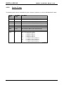
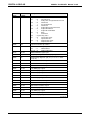
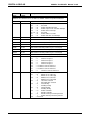
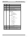
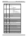
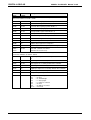
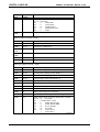
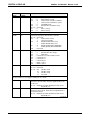
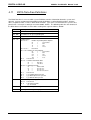
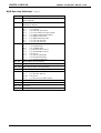
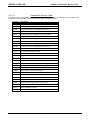
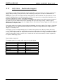
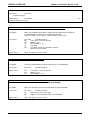
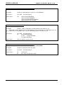
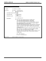
Locations 00h - 0Fh contain real time clock (RTC) and status information
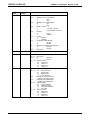
Locations 10h - 2Fh contain system configuration data
Locations 30h - 3Fh contain System BIOS-specific configuration data as well as chipset-specific information
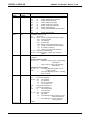
Locations 40h - 7Fh contain chipset-specific information as well as power management configuration
parameters
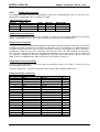
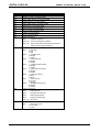
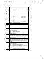
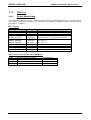
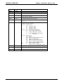
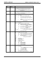
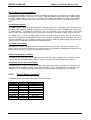
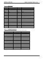
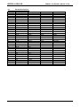
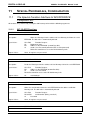
The following table provides a summary of how these areas may be further divided.
Beginning
Ending
Checksum
Description
00h
10h
2Eh
30h
34h
40h
5Ch
5Eh
6Fh
7Eh
0Fh
2Dh
2Fh
33h
3Fh
5Bh
5Dh
6Eh
7Dh
7Fh
No
Yes
No
No
No
Yes
No
No
Yes
No
RTC and Checksum
System Configuration
Checksum Value of 10h - 2Dh
Standard CMOS
Standard CMOS - SystemSoft Reserved
Extended CMOS - Chipset Specific
Checksum Value of 40h - 5Bh
Extended CMOS - Chipset Specific
Extended CMOS - Power Management
Checksum Value of 6Fh - 7Dh
41