1
®
®
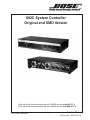
802C System Controller
Original and SMD Version
Units with serial numbers beginning with 100000 are the original 802C's.
Units with serial numbers beginning with 200000 are the new SMD 802C's.
©
1997 Bose Corporation
1
Service Manual
Part Number 129292 REV 03
Contents
Safety Information ............................................................................................................................ 3
Electrostatic Discharge Sensitive (ESDS) Device Handling ........................................................ 4
Specifications ................................................................................................................................... 5
Technical Description ...................................................................................................................... 6
Disassembly/Assembly Procedures .............................................................................................. 7
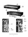
Figure 1. Locking Tab Screw Location ............................................................................................. 7
Figure 2. Original 802C PCB Exploded View ................................................................................... 8
Figure 3. SMD 802C PCB Exploded View ....................................................................................... 8
Test Procedures .......................................................................................................................... 9-10
Part List Notes ................................................................................................................................ 11
Main Part List .................................................................................................................................. 12
Figure 4. Main Parts Exploded View .............................................................................................. 13
Electrical Part List ..................................................................................................................... 14-17
Voltage Conversion Instructions .................................................................................................. 18
Figure 5. Voltage Conversion Diagram .......................................................................................... 18
Figure 6. Top Cover Connection Diagram ...................................................................................... 19
2
SAFETY INFORMATION
1. Parts that have special safety characteristics are identified by the
symbol on
schematics or by special notes on the parts list. Use only replacement parts that
have critical characteristics recommended by the manufacturer.
2. Make leakage current or resistance measurements to determine that exposed
parts are acceptably insulated from the supply circuit before returning the unit
to the customer. Use the following checks to perform these measurements:
A. Leakage Current Hot Check-With the unit completely reassembled, plug
the AC line cord directly into a 120V AC outlet. (Do not use an isolation
transformer during this test.) Use a leakage current tester or a metering
system that complies with American National Standards Institute (ANSI)
C101.1 “Leakage Current for Appliances” and Underwriters Laboratories
(UL) 1492 (71). With the unit AC switch first in the ON position, then in the
OFF position, measure from a known earth ground (metal water pipe,
conduit, etc.) to all exposed metal parts of the unit (antennas, handle bracket,
metal cabinet, screwheads, metallic overlays, control shafts, etc.), especially
any exposed metal parts that offer an electrical return path to the chassis.
Any current measured must not exceed 0.5 milliamp. Reverse the unit power
cord plug in the outlet and repeat test. ANY MEASUREMENTS NOT WITHIN
THE LIMITS SPECIFIED HEREIN INDICATE A POTENTIAL SHOCK HAZARD THAT MUST BE ELIMINATED BEFORE RETURNING THE UNIT TO
THE CUSTOMER.
B. Insulation Resistance Test Cold Check-(1) Unplug the power supply and
connect a jumper wire between the two prongs of the plug. (2) Turn on the
power switch of the unit. (3) Measure the resistance with an ohmmeter between the jumpered AC plug and each exposed metallic cabinet part on the
unit. When the exposed metallic part has a return path to the chassis, the
reading should be between 1 and 5.2 Megohms. When there is no return path
to the chassis, the reading must be “infinite”. If it is not within the limits specified,
there is the possibility of a shock hazard, and the unit must be repaired and rechecked before it is returned to the customer.
PROPRIETARY INFORMATION
THIS DOCUMENT CONTAINS PROPRIETARY INFORMATION OF
BOSE® CORPORATION WHICH IS BEING FURNISHED ONLY FOR
THE PURPOSE OF SERVICING THE IDENTIFIED BOSE PRODUCT
BY AN AUTHORIZED BOSE SERVICE CENTER OR OWNER OF THE
BOSE PRODUCT, AND SHALL NOT BE REPRODUCED OR USED
FOR ANY OTHER PURPOSE.
3
ELECTROSTATIC DISCHARGE SENSITIVE (ESDS)
DEVICE HANDLING
This unit contains ESDS devices. We recommend the following precautions when repairing,
replacing or transporting ESDS devices:
• Perform work at an electrically grounded work station.
• Wear wrist straps that connect to the station or heel straps that connect to conductive floor
mats.
• Avoid touching the leads or contacts of ESDS devices or PC boards even if properly
grounded. Handle boards by the edges only.
• Transport or store ESDS devices in ESD protective bags, bins, or totes. Do not insert unprotected devices into materials such as plastic, polystyrene foam, clear plastic bags, bubble wrap
or plastic trays.
CAUTION: THE 802®C SYSTEM CONTROLLER CONTAINS NO USER-SERVICEABLE
PARTS. TO PREVENT WARRANTY INFRACTIONS, REFER SERVICING TO WARRANTY
SERVICE STATIONS OR FACTORY SERVICE.
4
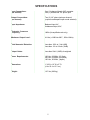
SPECIFICATIONS
Input Connections:
(per channel)
One (1) balanced female XLR connector
One (1) unbalanced 1/4" phone jack
Output Connections:
(per channel)
Two (2) 1/4" phone jacks per channel
(outputs used depend upon mode selected)
Input Impedance:
Balanced input, 4kΩ
Unbalanced input, 42kΩ
Electronic Crossover
Frequency:
180Hz (bi-amplified mode only)
Maximum Output Level:
4 Volts (+12dB into 600Ω, 50Hz-16kHz)
Total Harmonic Distortion:
Less than .02% at 1 Volt (0dB)
Less than .2% at 8 Volts (18dB)
Output Noise:
Less than 20uV (-9dBV) A-weighted
Power Requirements:
120 Vac, 50-60Hz, 3.5 Watts
220 Vac, 50-60Hz, (European)
100 Vac, 50-60Hz, (Japan)
Dimensions:
1 3/4"H x 10" W x 5" D
(4.4 x 25.4 x 12.7 cm)
Weight:
1.97 lbs (.895 kg)
5
TECHNICAL DESCRIPTION
The 802®C System Controller is a sophisticated signal processing device which combines the
functions of three equalizers, an automatic switching circuit, and an electronic crossover. The
802C system controller automatically selects the proper crossover function and equalization
curve for a given system application through use of a switching network operating in conjunction with the unit's output jacks. In addition to signal routing based on equalization requirements, the switching network indicates mode of operation on its front panel. The front panel
also includes high-cut and low-cut switches which decrease line output by 4dB at 55Hz and by
10dB at 16kHz. Sharp subsonic and ultrasonic band-limiting filters reduce power waste, stage
noise, high-frequency instability, and interference. The 802C system controller retains the
compact dimensions of its predecessor, the Bose® 802E active equalizer, and fits into one
space of a standard 19" equipment rack with the optional RMK-8 Rack Mount Kit.
In an on-going process of manufacturing updates, as technology permits, Bose Corporation
has begun using SMD (surface mount devices) components on its 802C controller. The new
SMD components are such a space saving feature that this new version permits us to eliminate the "piggy-back" PCB and place all electronics on one single printed circuit board. This
manual will identify the different procedures, PCB layouts, and components where necessary.
There is no difference in the operation or function between the original 802C and the
802C SMD units.
6
DISASSEMBLY/ASSEMBLY PROCEDURES
Note: Refer to the Figures (2 and 3) for the
following procedures.
4.2 Perform procedure 2.
5. Main PCB Removal
1. Top Cover Removal
5.1 Perform procedure 1.
1.1 Remove the four screws (two located
at the rear of the unit and one located on
each side of the unit) that secure the top
cover to the chassis.
5.2 Remove the 6 knurled nuts securing
the input and output jacks to the chassis.
5.3 Remove the 5 screws that secure the
main PCB to the chassis.
1.2 Lift the rear of the top cover slightly
and slide it forward until the front of the top
cover is clear of the switches.
5.4 On the rear of the unit, at the XLR
jacks there is a small hole with a locking
screw inside (see Figure 1). Insert a small
flathead screwdriver into the hole and
rotate the locking screw 1/8 turn counterclockwise to release the locking tab.
2. Top Cover Replacement
2.1 Align the front of the top cover with the
switches and LED's and slide the cover into
place.
5.5 Lift the front of the PCB up slightly.
Gently pull the PCB out while pushing on
the center of the XLR jacks.
2.2 Secure the top cover into place.
3. 302EQ ("piggy-back") PCB Removal
6. Main PCB Replacement
Note: The original 802C has two PCB's.
The following procedure will discuss the
removal of the "piggy-back" PCB.
6.1 Carefully slide the PCB into the chassis while aligning the XLR jacks into their
housing.
Note: The "piggy-back" PCB does not
need to be removed when removing the
main PCB.
6.2 Lock the XLR jacks into place by
inserting a small screwdriver into the small
hole in the XLR jack and rotate the screw
clockwise 1/8 turn.
3.1 Perform procedure 1.
3.2 Locate the four plastic stand-offs (three
are located in the corners of the PCB and
one is located between C125 and C225).
6.3 Replace the 5 screws that hold the
PCB into place in the chassis.
6.4 Perform procedure 2.
3.3 With small needle-nose pliers, squeeze
the retaining tab of each stand-off while
gently lifting up on the PCB to release the
lock. Grasp the PCB at the middle of each
side and lift the PCB off of the connectors.
4. 302EQ ("piggy-back") PCB Replacement
4.1 Replace the "piggy-back" PCB (on the
original 802C controller) by placing the
board over the connectors and pushing the
board down onto the stand-offs.
Figure 1. Locking Tab Screw Location
7
Figure 2. Original 802C PCB Exploded View
Figure 3. SMD 802C PCB Exploded View
8
TEST PROCEDURES
Note: Set both the Lo and Hi cut switches
IN for the following response table.
1. Mode Indicator Test
Lo and Hi Cut Switch Response Table
1.1 Depending on the output jack configuration (see top cover diagram on page 17),
equalization curves and output vary. You
must test all modes of the 802C to assure
proper operation.
Frequency
55Hz
750Hz
15kHz
1.2 Perform the test below to verify that the
mode select operation is working properly.
Tolerance
± 1.8dB
± 2.0dB
3. 302 Passive Frequency Response
3.1 Apply a 750Hz, 500mVrms signal to
the input of the 802C.
Note: You can insert one or both of the
output jacks into the unit for this test.
3.2 Reference a dB meter to the 302 AMP
output jacks.
LED Indicator Status
Output
Jacks
Inserted
No Jacks
Inserted
Inserted into
802 AMP
Inserted into
302 AMP
Inserted into
802 and 302
AMP
Output
+9.3dB
0dB
(reference)
+6.9dB
802
Full
Range
On
Passive
2-Way
BiAMP
Off
Off
On
Off
Off
Off
On
Off
Off
Off
On
3.3 Refer to the frequency response table
below and verify the response of the unit.
Passive Frequency Response Table
Frequency
30Hz
55Hz
150Hz
250Hz
750Hz
3kHz
15kHz
2. 802 Full Range Frequency Response
2.1 Apply a 750Hz, 500mVrms signal to
the input of the 802C.
Output
-8.8dB
+6.2dB
-3.2dB
+3.2dB
0 dB
(reference)
0.9dB
+15.3dB
Tolerance
± 2.5dB
± 1.5dB
± 1.5dB
± 1.8dB
± 1.5dB
± 1.8dB
4. Bi-Amp Frequency Response
2.2 Reference a dB meter to the 802 AMP
output jacks.
Note: This test is performed with both the
802 AMP and the 302 AMP output jacks
used at the same time.
2.3 Refer to the frequency response table
below and verify the response of the unit.
4.1 Apply a 750Hz, 500mVrms signal to
the input of the 802C.
Full Range Frequence Response Table
Frequency
Output
Tolerance
55Hz
+14.0dB
± 1.5dB
30Hz
0dB
± 2.5dB
250Hz
+2.7dB
± 1.2dB
750Hz
0dB
(reference)
3kHz
+2.3dB
± 1.5dB
7.5kHz
+12.0dB
± 1.5dB
15kHz
+16.9dB
± 1.8dB
4.2 Reference a dB meter to the 802 AMP
output jacks (while in the Bi-Amp mode).
4.3 Refer to the frequency response table
below and verify the response of the unit.
802 Bi-Amp Frequency Response Table
Frequency
Output
Tolerance
55Hz
-20.1dB
± 2.5dB
230Hz
+2.6dB
± 1.8dB
750Hz
0 dB
(reference)
15kHz
+17.0dB
± 1.8dB
9
TEST PROCEDURES
4.4 Apply a 100Hz, 500mVrms signal to
the input of the 802C.
6. Noise Test
4.5 Reference a dB meter to the 302 AMP
output jacks (while in the Bi-Amp mode).
6.1 All noise measurements are ANSI
A-weighted true rms, with the inputs
shorted.
4.6 Refer to the frequency response table
below and verify the response of the unit.
6.2 Refer to the table below for the proper
noise levels.
302 Bi-Amp Frequency Response Table
Frequency
55Hz
100Hz
Output
+3.7dB
0dB
(reference)
-8.3dB
-25.8dB
230Hz
750Hz
Noise Table
Output
Noise
802 Full
<20uV
Range
302 Passive
<20uV
802 Bi-Amp
<20uV
302 Bi-Amp
<10uV
Tolerance
± 1.5dB
± 1.5dB
± 2.5dB
5. Distortion Test
Note: Total harmonic distortion must be
measured in all modes to assure proper
operation.
5.1 Apply a 750Hz, 5Vrms signal to the
input of the 802C.
5.2 Refer to the table below for the distortion specification for the corresponding
mode being tested.
Note: For the Bi-Amp 302 reading the
input signal should be a 100Hz, 5Vrms
signal.
Distortion Table
Output
802 Full
Range
302 Passive
802 Bi-Amp
302 Bi-Amp
Frequency. Distortion
750Hz
<0.1%
750Hz
750Hz
100Hz
<0.1%
<0.1%
<0.1%
10
PART LIST NOTES
1. This part is not normally available from Customer Service. Approval from the Field Service
Manager is required before ordering.
2. The individual parts located on the PCB are listed in the Electrical Part List.
3.
This part is critical for safety purposes. Failure to use a substitute replacement with
the same safety characteristics as the recommended replacement part might create shock, fire
and or other hazards.
4. RC-4156 is to be used ONLY as a replacement for U5 and U6. This replaces the selected
LS-404 IC previously used in these locations. Due to the higher current needs of the RC-4156,
DAMAGE could occur to the power supply if this IC is used in other locations on the PCB.
5. This part is used on the 220V variation only.
11
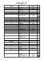
MAIN PART LIST
Item
Number
1
2
3
4
5
6
7
8
9
10
11
12
13
14
15
16
17
Reference
Designator
J1, 3
J2, 4-8
J9
J9
J10
J10
P1, 2
T1
(See Figure 4)
Description
COVER
CHASSIS
FEET
SCREW, SHEET METAL,
4-40 x .25L
CONNECTOR, XLR
NUT, KNURLED
STRAIN RELIEF BUSHING
LINE CORD, 100/120V
LINE CORD, 220V
LED
BRACKET, LED
SMD PCB ASSEMBLY
SWITCH, KNOB
SWITCH, DUAL
SCREW, MACHINE, 4-40
x .187L
STANDOFF
PCB ASSEMBLY (TOP)
PCB ASSEMBLY (MAIN)
CARTON
FILLER
POLY BAG
ACCESSORY KIT
MTG KIT (802 COVER)
SWITCH, SLEEVE
INSULATOR
SCREW, MACHINE,
NYLON,
6-32 x .75L, 220V
SCREW, MACHINE,
NYLON,
6-32 x .25L, 220V
STANDOFF, HEX, 6 x
.375L
Description
CONNECTOR, XLR,
INSERT
JACK, PHONE
WAFER, 7PIN, (2461)
CONNECTOR, 7PIN
(21458)
WAFER, 6PIN (2461)
CONNECTOR, 6PIN
(21458)
TEMINAL, FASTON
TRANSFORMER,
110/220V
TRANSFORMER, 120V
TRANSFORMER, 100V
12
Part
Number
135040
133230
103593
103118-04
121810
121890
106346
111672
113608
123487
120975
120989
107461
103140-03
123199
122068
121860
122640
100688
121783
123037
120996
122855
124843-12
Note
1
3
1
1
1
5
128843-04
5
121828-06
5
Part Number
Note
121823
121570
123237-07
121970-07
123237-06
121970-06
111262
3
120993
3
121659-1
121824
Figure 4. Main Parts Exploded View
13
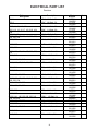
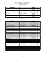
ELECTRICAL PART LIST
Resistors
Reference
Designator
Description
R1, 2
2.7kΩ, 1/4 Watt, 5%
R3, 4
3.3kΩ, 1/4 Watt, 5%
R5-7, 11, 15, 118, 218
160kΩ, 1/4 Watt, 5%
R8, 9, 12, 13, 16, 17, 101, 210, 104,
204
R10, 14, 18
R102, 103, 105, 122, 124, 202, 203,
205, 222, 224
R106, 206
330kΩ, 1/4 Watt, 5%
R107, 207
48.7kΩ, 1/4 Watt, 1%
R108, 208
20kΩ, 1/4 Watt, 5%
R109, 126, 130, 131, 209, 226, 230,
231
R110, 210
23.7kΩ, 1/4 Watt, 1%
R111, 113, 211, 213
1kΩ, 1/4 Watt, 5%
R112, 146, 152, 212, 246, 252
4.75kΩ, 1/4 Watt, 1%
R114, 214
13kΩ, 1/4 Watt, 2%
R115, 215
10kΩ, 1/4 Watt, 5%
R116, 125, 216, 225
8.2kΩ, 1/4 Watt, 2%
R117, 128, 129, 133, 134, 217, 228,
229, 233, 234
R119, 120, 219, 220
6.81kΩ, 1/4 Watt, 1%
18kΩ, 1/4 Watt, 5%
R121, 136, 221, 236
22kΩ, 1/4 Watt, 5%
R123, 223
470Ω, 1/4 Watt, 5%
R127, 227
130kΩ, 1/4 Watt, 5%
R132, 141, 145, 153-158, 232, 241,
245, 253-258
R135, 159, 235, 259
R137, 237
6.04kΩ, 1/2 Watt, 1%
510Ω, 1/4 Watt, 5%
47.5kΩ, 1/4 Watt, 1%
R138, 140, 238, 240
15.0kΩ, 1/4 Watt, 1%
R142, 242
3.0kΩ, 1/4 Watt, 1%
R143, 243
33kΩ, 1/4 Watt, 5%
8.2kΩ, 1/2 Watt, 5%
2.00kΩ, 1/4 Watt, 1%
1.9kΩ, 1/4 Watt, 1%
2.74kΩ, 1/4 Watt, 1%
14
Part
Number
1177041212725
1177041213325
1177041211645
1177041213345
122071-8225
1199762212001
1199762211911
1199762214872
1177041212035
1199762212372
1199762212741
1177041211025
1199762214751
1177041211332
1177041211035
1177041218222
1199762216811
1177041211835
1177041212235
1177041214715
1177041211345
1199762216041
122071-5115
1199761214752
1199762211502
1199762213011
1177041213335
Note
ELECTRICAL PART LIST
Resistors (continued)
Reference
Designator
Description
Part
Number
1177041215632
1199762214121
1199762212372
1199762213092
1177041212235
Note
Note
2.7kΩ, CHIP, 5%
3.3kΩ, CHIP, 5%
160kΩ, CHIP, 5%
330kΩ, CHIP, 5%
2.00kΩ, CHIP, 1%
Part
Number
124895-2725
124895-3325
124895-1645
124895-3345
124894-2001
1,91kΩ, CHIP, 1%
48.7kΩ, CHIP, 1%
20kΩ, CHIP, 5%
23.7kΩ, CHIP, 1%
124894-1911
124894-4872
124895-2035
124894-2372
2.74kΩ, CHIP, 1%
13.3kΩ, CHIP, 1%
1kΩ, CHIP, 5%
10kΩ, CHIP, 5%
8.25kΩ, CHIP, 1%
124894-2741
124894-1332
124895-1025
124895-1035
124894-8251
6.81kΩ, CHIP, 1%
124894-6811
18kΩ, CHIP, 5%
22kΩ, CHIP, 5%
470Ω, CHIP, 5%
130kΩ, CHIP, 5%
6.04kΩ, CHIP, 1%
124895-1835
124895-2235
124895-4715
124895-1345
124894-6041
47.5kΩ, CHIP, 1%
3.01kΩ, CHIP, 1%
33kΩ, CHIP, 5%
56.2kΩ, CHIP, 1%
4.75kΩ, CHIP, 1%
26.7kΩ, CHIP, 1%
124894-4752
124894-3011
124895-3335
124894-5622
124894-4751
124894-2672
R144, 244
56kΩ, 1/4 Watt, 2%
R148, 248
4.12kΩ, 1/4 Watt, 1%
R149, 249
23.7kΩ, 1/4 Watt, 1%
R150, 250
30.9kΩ, 1/4 Watt, 1%
R160, 260
22kΩ, 1/4 Watt, 5%
SMD Resistors
Reference
Designator
R1, 2
R3, 4
R5, 6, 7, 11, 15, 118, 218
R8, 9, 12, 13, 16, 101, 104
R102, 103, 105, 111, 122, 124, 202,
203, 205, 211, 222, 224
R106, 206
R107, 207
R108, 208
R109, 126, 130, 131, 209, 226, 230,
231
R110, 210
R112, 114, 212, 214
R113, 213
R115, 215
R116, 125, 139, 152, 216, 225, 239,
252
R117, 128, 129, 133, 134, 217, 228,
229, 233, 234
R119, 120, 219, 220
R121, 136, 160, 221, 236, 260
R123, 223
R127, 227
R132, 141, 145, 147, 151, 153-158,
232, 241, 245, 247, 251, 253-258
R137, 237
R142, 242
R143, 149, 150, 234, 249, 250
R144, 244
R146, 246
R164, 264
Description
15
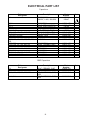
ELECTRICAL PART LIST
Capacitors
Reference
Designator
Description
C1
.0047uF, 220V
.0047uF, 1.4KV, 100/120V
Part
Number
120993
103447
C2, 3
C4
C5, 6
C7-10
C11-19, 22
C101, 117, 125, 201, 217, 225
C102, 202
C103-105, 203-205
C106, 206
C107, 108, 121, 122, 207, 208, 221,
222
C109, 209
C110, 126, 127, 210, 226, 227
C111, 211
C112, 113, 124, 212, 213, 224
C114, 214
C115, 116, 123, 215, 216, 223
C118, 119, 218, 219
C120, 220
.015uF, FILM
.01uF, CERAMIC DISC
470uF, ELECTROLYTIC
1uF, ELECTROLYTIC
.1uF, CERAMIC DISC
22uF, ELECTROLYTIC
2.2uF, ELECTROLYTIC
.0068uF, FILM
.33uF, FILM
.1uF, FILM
118091-153
119696-103
110704
119942-1R0
117502
119944-220
119943-2R2
118091-682
123785-334
118091-104
.0012uF, FILM
470pF, CERAMIC DISC
270pF, CERAMIC DISC
.033uF, FILM
.068uF, FILM
.047uF, FILM
.082uF, FILM
.022uF, FILM
118091-122
119617-471
119617-271
118091-333
118091-683
118091-473
118091-823
118091-223
Note
3
SMD Capacitors
Reference
Designator
C4
C11-22
C110, 126, 127, 210, 226, 227
C111, 211
Description
.01uF, CERAMIC, CHIP
.1uF, CERAMIC, CHIP
470pF, CERAMIC, CHIP,
10%
270pF, CERAMIC, CHIP,
10%
16
Part
Number
124959-103
124959-104
124956-4712
124956-2742
Note
ELECTRICAL PART LIST
Diodes
Reference
Designator
D1-5
D1, 101, 104, 201-204
Z1
Description
ZENER, 18V, 1W, IN4746A
1N4148, DIODE
BRIDGE RECTIFIER
Part
Number
116995-4746A
121501
112027
Note
Part
Number
117921
119168
Note
Part
Number
120535/192166
121116-1
121117-1
121854
192166
119837
Note
3
Transistors
Reference
Designator
Q1, 4, 5
Q2, 3, 6
Description
TRANSISTOR NPN
TRANSISTOR PNP
Integrated Circuits
Reference
Designator
U1, 8, 9
U2
U3
U4
U5, 6
U7, 10
Description
QUAD OP AMP, LS-404
VOLT REG, 78L15
VOLT REG, 79L15
QUAD NAND CD-4011
QUAD OP AMP, RC4156
QUAD AW. SW. CD4066
Part Number change for U2 and U3
9/18/01 Also U5 and U6 has been replaced by part number
192166 which is an LS404 IC. The RC4156 is nolonger available.
17
4
4
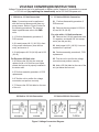
VOLTAGE CONVERSION INSTRUCTIONS
Voltage Conversions are to be performed on Military units. However it is possible to convert
a 110 Volt unit (by replacing the transformer) and a 220 Volt European unit.
1. 220 Volt to 110 Volt Conversion
2. 110 Volt to 220 Volt Conversion
Note: Conversions must be performed
with the line cord disconnected from any
power source. Refer to Figure 3 below for
the following procedures. The jumpers
listed in parentheses refer to the SMD
units.
2.1 Perform disassembly procedure 3,
PCB removal.
2.2 Remove the two jumpers LK-32 (LK42) and LK-33 (LK-43).
For units with a 110 Volt transformer.
2.2 Remove the 110 Volt transformer and
C1 capacitor, and install 220 Volt components (see the part list).
1.1 Perform disassembly procedure 3,
PCB removal.
1.2 Locate jumper LK-31, (LK-35) in front
of the power transformer (near the line
cord), and remove it.
2.3 Add jumper LK-31 (LK-35). Line cord
replacement is optional.
1.3 Add jumpers LK-32 (LK-42) and LK-33
(LK-43).
2.4 Perform assembly procedure 4, PCB
replacement.
For European 220 Volt units.
1.4 Remove the 220 Volt line cord and
replace it with a 110 Volt line cord. Make
certain the line cord is properly installed in
the strain relief.
2.5 Test the unit to confirm the voltage
conversion was perform correctly.
2.6 Add a 220 Volt label on the rear of the
unit just below the line cord.
1.5 Perform assembly procedure 4, PCB
replacement.
1.6 Test the unit to confirm the voltage
conversion was perform correctly.
1.7 Remove the 220 Volt label on the rear
of the unit.
220 Volt to 110 Volt Conversion
110 Volt to 220 Volt Conversion
Figure 5. Voltage Conversion Diagram
18
Figure 6. Top Cover Connection Diagram
19
SPECIFICATIONS AND FEATURES SUBJECT TO CHANGE WITHOUT NOTICE
®
®
Bose Corporation
The Mountain
Framingham Massachusetts USA 01701
P/N 129292 REV. 03 10/97 FOR TECHNICAL ASSISTANCE OR PART ORDERS, CALL 1-800-367-4008