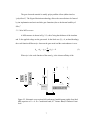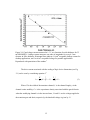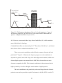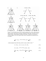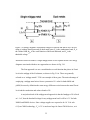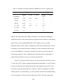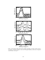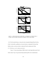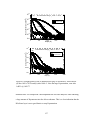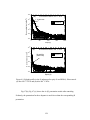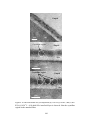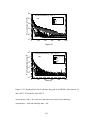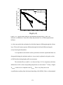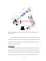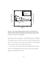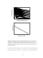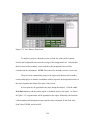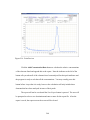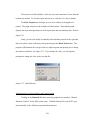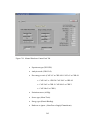
1
MATERIALS PROPERTIES OF HAFNIUM AND ZIRCONIUM SILICATES: METAL INTERDIFFUSION AND DOPANT PENETRATION STUDIES Manuel Angel Quevedo Lopez BS. MS. Dissertation Prepared for the Degree of DOCTOR OF PHILOSOPHY UNIVERSITY OF NORTH TEXAS August 2002 APPROVED: Robert M. Wallace, Major Professor Bruce E. Gnade, Major Professor and Chairman of the Materials Science Department Luigi Colombo, Committee Member Mohamed El Bouanani Committee Member Jeffrey Kelber, Committee Member Oscar Mendoza, Committee Member Witold Brostow, Coordinator of the Program in Materials Science C. Neal Tate, Dean of the Robert B. Toulouse School of Graduate Studies Quevedo-Lopez, Manuel Angel, Materials properties of hafnium and zirconium silicates: metal interdiffusion and dopant penetration studies. Doctor of Philosophy (Materials Science), August 2002, 278 pages, 10 tables, 142 figures, references. Hafnium and Zirconium based gate dielectrics are considered potential candidates to replace SiO2 or SiON as the gate dielectric in CMOS processing. Furthermore, the addition of nitrogen into this pseudo-binary alloy has been shown to improve their thermal stability, electrical properties, and reduce dopant penetration. Because CMOS processing requires high temperature anneals (up to 1050 °C), it is important to understand the diffusion properties of any metal associated with the gate dielectric in silicon at these temperatures. In addition, dopant penetration from the doped polysilicon gate into the Si channel at these temperatures must also be studied. Impurity outdiffusion (Hf, Zr) from the dielectric, or dopant (B, As, P) penetration through the dielectric into the channel region would likely result in deleterious effects upon the carrier mobility. In this dissertation extensive thermal stability studies of alternate gate dielectric candidates ZrSixOy and HfSixOy are presented. Dopant penetration studies from dopedpolysilicon through HfSixOy and HfSixOyNz are also presented. Rutherford backscattering spectroscopy (RBS), heavy ion RBS (HI-RBS), x-ray photoelectron spectroscopy (XPS), high resolution transmission electron microscopy (HR-TEM), and time of flight and dynamic secondary ion mass spectroscopy (ToF-SIMS, D-SIMS) methods were used to characterize these materials. The dopant diffusivity is calculated by modeling of the dopant profiles in the Si substrate. In this disseration is reported that Hf silicate films are more stable than Zr silicate films, from the metal interdiffusion point of view. On the other hand, dopant (B, As, and P) penetration is observed for HfSixOy films. However, the addition of nitrogen to the Hf – Si – O systems improves the dopant penetration properties of the resulting HfSixOyNz films. Copyright 2002 by Manuel Angel Quevedo Lopez ii ACKNOWLEDGMENTS It was a very uncertain time in my life when I just arrived to UNT, no plan for the future, and few acquaintances in the department to offer an advice in choosing a field. However, in my second year I was under economic pressure and I asked for additional work to Prof. Bruce Gnade. Everything in my life has changed ever since. It has been more than 3 years ago already! At that time it was not clear what I will do. Only after I started working in the lab did I realize that I was working in one of a few labs in the world with a complete setup to do real applied materials research, especially in the area that I have loved since my college days: semiconductors. I have a long list of persons to thank for helping me to achieve this important goal in my life. First of all, my advisor: Prof. Robert M. Wallace (or Bob as he likes to be called), one of the most talented physicists in the field of semiconductor devices and silicon technology. His advising style makes you feel that you always have something to learn, new challenges, and new problems to solve. I found this very appropiate for the kind of work that we do at LEMD. I learned that without effort there is in no reward…nothing is free. He showed me in an elegant way that hardwork is the secret to be successful. Thanks. Prof. Bruce Gnade is one of the most important reasons I’m now graduating from LEMD. He gave me the opportunity to join the laboratory. I will always be grateful for that opportunity. Bruce, like you said: “It has been a long journey since the first day…when we formatted the XPS hard drive,” but believe me, I have really enjoyed working with you. It’s been my pleasure. I would also like to thank Prof. Mohamed El-boananai. He was always there to offer me continuous support not only academic, but also as a friend. His way of approaching the different research problems was extremely helpful for me. He was patient and trusted in me when learning ion beam analysis; this allows me to slowly explore in this new field and build confidence with myself through all the successes and mistakes. I thank the committee members for reading this dissertation, Dr. Oscar Mendoza, Dr. Jeff Kelber, Dr. Luigi Colombo. Thanks for your intelligent advice in making this manuscript more “reader friendly”. I would also like to thank my friends at LEMD, UNT and the Staff (by strict alphabetic order): Dr.Swarna Addepalli, Tommy Benett, Alberta Caswell, Dr. J. Duggan, Alex Hernandez, Dr. M. Kim, Dr. Oscar Mendoza, Billy Roulston, G. Pant, and Dr. P. Punchaipetch. It would not be fair not to thank two persons from Texas Instruments that always offered me support: Dr. Luigi Colombo and Dr. Mark Visokay. Thanks for you continuous help. Lastly, but by far not the least, I would like to thank my family for being always very supportative to my stubborn pursuit to become a scientist. Looking back, I really thank God for giving me such wonderful parents, a wonderful girlfriend (she knows what I mean), an excellent university, and the chance to work with all the wonderful people here at UNT. Thank you all. iii TABLE OF CONTENTS Page ACKNOWLEDGMENTS ............................................................................................... iii LIST OF TABLES ........................................................................................................... vii LIST OF ILLUSTRATIONS........................................................................................... viii Chapter 1. INTRODUCTION .............................................................................................. 2. LITERATURE REVIEW: GATE DIELECTRICS ............................................. 2.1 Transistors: Fundamentals ...................................................................... 2.1.1 The Basic MIS Structure ............................................................... 2.1.2 Ideal MIS structure ........................................................................ 2.2 The insulator in MIS structures: gate dielectrics .................................... 2.2.1 SiO 2 and SiON............................................................................... 2.2.2 The Need For Alternate Gate Dielectrics ...................................... 2.2.3 Equivalent Oxide Thickness Definition ........................................ 2.3 Alternate Gate Dielectrics: Required Materials Properties .................... 2.3.1 Permittivity And Barrier Height ................................................... 2.3.1.1 Factors Affecting κ............................................................ 2.3.2 High-κ Gate Dielectric Stability In Contact With Silicon............. 2.3.3 Interface Quality............................................................................ 2.3.4 Film Morphology........................................................................... 2.3.5 Gate Compatibility ........................................................................ 2.3.6 Process Compatibility.................................................................... 2.3.7 Reliability ...................................................................................... 2.4 Pseudobinary Alloys ............................................................................... 2.4.1 Recent Results on Zr and Hf Silicate Systems .............................. 2.5 Impurity Mobility on Effect on Device Performance............................. 2.6 References .............................................................................................. 3. LITERATURE REVIEW: DOPANT DIFFUSION IN Si AND GATE OXIDES ............................................................................................................... 3.1 Introduction ............................................................................................. 3.2 Diffusion Phenomena: Fick’s Law .......................................................... 3.3 Mechanisms of Diffusion in Solids: Point Defects .................................. 3.3.1 Native Point Defects ...................................................................... 3.3.2 Dopant Defects .............................................................................. 3.4. Dopant Diffusion in Si............................................................................ 3.5. Equations Solutions to Selected Diffusion Processes ............................. 3.5.1 Diffusion from Infinite Source on Surface ................................... iv 1 6 6 6 7 10 10 13 17 19 20 25 28 32 33 34 36 37 37 41 44 48 51 51 52 55 55 57 59 61 62 3.5.2 Diffusion from Limited Source on Surface................................... 62 3.5.3 Diffusion Through Thin Layer ...................................................... 63 3.6 Dopant Diffusion Through SiO2 Films: Review of Sah’s Model ........... 66 3.7 Dopant Diffusion Through SiO 2 And SiON ............................................ 68 3.7.1 Diffusion Defects in SiO 2 .............................................................. 69 3.7.2 Random Walk Diffusion in SiO 2 ................................................... 71 3.7.3 Dopant Diffusion in Nitrided Oxides ............................................ 72 3.7.4 Boron diffusion in SiO 2 and SiON ................................................ 74 3.7.5 Phosphorus and As Diffusion in SiO 2 and SiON .......................... 76 3.8 Dopant Diffusion Studies Through Alternate Gate Dielectrics ............... 76 3.9 References ................................................................................................ 80 4. WET CHEMICAL ETCHING STUDIES: Zr AND Hf-SILICATE GATE DIELECTRICS AND DOPED POLYSILICON................................................. 83 4.1 Introduction.............................................................................................. 83 4.2 Experimental............................................................................................ 86 4.3 Results and Discussion ............................................................................ 90 4.3.1 As Deposited Films: Zr and Hf-Silicates....................................... 90 4.3.2 ZrSix Oy and HfSix Oy Etching in Dilute HF ................................... 92 4.3.2.1 ZrSix Oy .............................................................................. 92 4.3.2.2 HfSix Oy .............................................................................. 94 4.3.3 ZrSix Oy and HfSix Oy Etching in Concentrated HF ........................ 95 4.3.3.1 HfSix Oy .............................................................................. 96 4.3.3.2 ZrSix Oy .............................................................................. 99 4.3.4 Heavy Ions RBS Analysis of Remnant Zr and Hf After Etching..103 4.4 Polysilicon Etching Study........................................................................110 4.4.1 Polysilicon Etching: Non-doped Polysilicon...............................110 4.4.2 Polysilicon Etching: Doped Polysilicon ......................................112 4.5 Conclusions ..............................................................................................115 4.6 References ................................................................................................116 5. THERMAL STABILITY STUDIES OF Zr AND Hf SILICATES ....................118 5.1 Introduction..............................................................................................118 5.2 Experimental............................................................................................120 5.3 Results and Discussion ............................................................................122 5.3.1 ZrSixOy Thermal Stability: Zr Incorporation from ZrSix Oy Films into Si.............................................................................................122 5.3.2 HfSix Oy Thermal Stability: Hf Incorporation Studies from HfSix Oy Films into Si...................................................................................133 5.4 Chemical Depth profiling of Zr and Hf Incorporation.............................141 5.5 Summary .................................................................................................143 5.6 Conclusions ..............................................................................................145 5.7 References ................................................................................................146 6. DOPANT PENETRATION STUDIES FROM DOPED POLYSILICON TROUGH CVD DEPOSITED HFSIXOY AND HFSION....................................148 6.1 Introduction..............................................................................................148 6.2 Experimental Details ................................................................................149 v 6.3 Results and Discussion Part 1: HfSix Oy films..........................................154 6.3.1 Not Annealed Films: SIMS....................................................154 6.3.3 Preliminary Results on Dopant Penetration...........................156 6.3.4 B-Doped Polysilicon..............................................................159 6.3.5 P-Doped Polysilicon ..............................................................163 6.3.6 As-Doped Polysilicon............................................................166 6.4 Diffusivities Calculations: Modeling .......................................................168 6.4.1 Modeling Results: Boron Penetration....................................171 6.4.2 Modeling Results: P Penetration............................................175 6.4.3 Modeling Results: As Penetration .........................................178 6.5 Summary: Dopant Penetration Through HfSix Oy Films ..........................179 6.6 Results and Discussion Part 2: HfSix Oy Nz Films.....................................180 6.6.1 Introduction............................................................................180 6.6.2 Experimental Details ..............................................................181 6.6.3 B, P and As Penetration: Experimental Results .....................182 6.6.4 Dopant Penetration in HfSix Oy Nz: Modeling Results ............187 6.7 Comparison of Dopant Penetration Between HfSix Oy and HfSix OyN z ...188 6.8 Conclusions ..............................................................................................193 6.9 References ................................................................................................195 7. CONCLUSIONS AND FUTURE WORK ............................................................198 APPENDIX A. ...........................................................................................................200 APPENDIX B. ...........................................................................................................227 APPENDIX C. ...........................................................................................................242 APPENDIX D. ...........................................................................................................275 vi LIST OF TABLES Table Page 4.1 Remnant Zr concentrations (calculated by RBS) after ZrSix Oy removal with stirred 1% HF solutions.........................................................................................................93 4.2 Remnant Hf concentrations (calculated by RBS) after HfSix Oy removal with stirred 1% diluted HF solutions.............................................................................................94 4.3 Remnant Zr and Hf evaluated by HIRBS after UV/O 3 + etching cycles. (at/cm2 ). ...108 6.1 Dose and implant energies for the three dopants used in this study..........................150 6.2 Rapid thermal annealing matrix illustrating the different annealing conditions (temperature and time) for the dopant penetration studies ........................................151 6.3 SIMS analysis details. As analysis were carried out at Charles Evans Inc................153 6.4 Evaluated P diffusivities from the fittings shown in Fig. 19 .....................................178 6.5 Comparison of DP,HfSiO with DP,SiO2 and DP,SiON.........................................................178 6.6 Comparison of DAs,HfSiO with DAs,SiO2 ........................................................................180 6.7 Evaluated B diffusivity in HfSix Oy Nz at 1050 oC......................................................189 vii LIST OF ILLUSTRATIONS Figure Page 2.1. Schematic MIS transistor, which is alternatively called “MOS” since silicon oxide has been used as gate-dielectric film..........................................................................6 2.2. Schematic cross section (left) and energy band diagram (right) of an ideal MIS capacitor at VG = 0. ....................................................................................................7 2.3. Energy band diagrams of an ideal MIS capacitor with p-type semiconductor at VG ? 0 for a) accumulation, b) depletion and c) inversion conditions................................8 2.4. Structure of the Si/SiO 2 interface..............................................................................10 2.5. Schematic illustration of a CMOS-FET: complementary metal–oxide field effect transitor ......................................................................................................................11 2.6. Thermodynamic phase diagram (bulk) of the Si- O-N system. .................................13 2.7. Decrease in gate SiO 2 thickness with device scaling technology generation vs. actual or expected year of implementation of each technology generation. ........................14 2.8. Gate leakage current measured at 1.5 V as a function of oxide thickness for 35 nm NMOSFETs. ..............................................................................................................15 2.9. Energy-band diagrams and associated high- frequency C – V curves for ideal MIS diodes for a) n-type and b) p-type semiconductor substrates. ...................................21 2.10 . Calculated Band offsets for oxide in Si. .................................................................22 2.11. The frequency dependence of the real (ε r’) and imaginary (ε r’’) parts of the dielectric permittivity. ..............................................................................................23 2.12. Permittivity (κ) versus bandgap for oxides.............................................................24 2.13. The effect of a lower κ interface (near the Si surface) limits the total capacitance achieved with the new high-κ material. ...................................................................29 2.14. Comparison of (a) stacked and (b) single- layer gate dielectrics. ............................30 2.15. (a) The three types of M-Si-O phase diagrams (for systems with no ternary phases) viii and (b) a flowchart of reactions to identify to which type a particular M-Si-O system belongs ........................................................................................................31 2.16. Energy diagrams of threshold voltages for NMOS and PMOS FET devices using (a) midgap metal gates and (b) dual metal gates............................................................35 2.17.Ternary phase diagram for a) Ta – Si – O, b) Ti – Si – O, and c) Zr – Si – O ........38 2.18. Structure of crystalline ZrSiO 4 showing the Zr bonding to SiO 2 units. Zr–O bonding also exists in and out of the plane of the page (not shown). ...................................40 2.19. Drift mobility of Ge, Si and GaAs at 300 oC vs impurity concentration ...............45 2.20. The different components of a transistor affected by metal out diffusion from alternate gate dielectrics ...........................................................................................46 3.1. Jumping of atoms from plane to plane ......................................................................53 3.2.Vacancy, interstitial, and interstitialcy point defects. ................................................56 3.3. Schematic two-dimensional representation of (a) direct and (b) indirect diffusion mechanisms of an element A (denoted by the open circle) in a solid. .....................57 3.4. Temperature dependence of the diffusion coefficient of foreign atoms (A) in silicon, compared with self-diffusion. ...................................................................................60 3.5.Typical profiles (in linear scale) of the C/C 0 dependence with Dt1/2 .........................63 3.6. Diffusion through thin layer into infinitely thick layer of different material. ..........64 3.7. The concentration profile of diffusing dopant in SiO 2 and the concentration profile in Si. ..............................................................................................................................66 3.8. Schematic representation of calculated atomic positions for the peroxy precursor with initial Si- Si separation of 5.2 Å. .......................................................................70 3.9. Intrinsic dopant diffusion in pure SiO 2 via the peroxy linkage defect......................71 3.10. Schematic drawing showing the competition between nitrogen and boron for diffusion activation through a PLD site. .................................................................74 4.1.High-vacuum furnace constructed to anneal the Hf and Zr silicate films. ................85 4.2. a) Typical ramp times for the furnace shown in Fig. 4.1. .........................................86 ix 4.3. Experimental flow diagram fo r the etching studies of Hf and Zr silicate films. ......87 4.4. RBS setup used to improve the Zr and Hf sensitivity...............................................89 4.5. XPS and HRTEM of as-deposited films. ..................................................................90 4.6. Zr and Hf distribution across the wafer, as evaluated by RBS. ................................91 4.7. RBS spectra of typical etch time studies carried out in this study............................97 4.8. Remnant Hf after HfSix Oy removal as a function of annealing temperature. ...........99 4.9. Remnant Zr after ZrSix Oy removal, as a function of annealing temperature. ...........100 4.10. a) Remnant Zr as a function of RTA (1050 o C) annealing time, and b) as function of furnace annealing temperature. ...............................................................................102 4.11.Chemical depth profiling experimental flow diagram. ............................................103 4.12. SiO 2 thickness grown after UV/O 3 oxidation for different times. ..........................104 4.13. HI-RBS results for a) Furnace annealed and RTA annealed Hf silicate films .......105 4.14. Comparison between ToFSIMS results and chemical depth profiling. ..................106 4.15. (a) Zr 3d region for Zr silicate films after annealing and etching...........................107 4.16. Poly-Si removal with a) 80o C KOH and b) Room temperature (RT). ....................111 4.17. Dopant effect on poly-Si removal... ........................................................................113 4.18. XPS analysis of the films after poly-Si removal (B-doped) with KOH. ................114 5.1. HRTEM of a) as-deposited ZrSix Oy , b) furnace annealed (1100o C), and c) 180 s RTA (1050ºC) annealed ZrSix Oy prior to etching. ............................................................123 5.2. Zr silicate XPS results before and after RTA and furnace anneling. a) Zr3d, b) Si2p, and c) O1s regions. ..................................................................................................126 5.3. RBS results for annealed and etched ZrSix Oy films..................................................130 5.4. ToF-SIMS depth profiles of the as-deposited and furnace annealed/etched ZrSix Oy dielectric films. .........................................................................................................132 5.5. HRTEM images of HfSix Oy films prior to any etching. ...........................................134 x 5.6. Hf silicate XPS results before and after annealing ...................................................136 5.7. RBS results for annealed/etched HfSix Oy films. (a) 6 min furnace anneal, (b) RTA at 1050 o C.....................................................................................................................138 5.8. ToF-SIMS depth profiles of the as-deposited and furnace annealed/etched HfSix Oy dielectric films. .........................................................................................................139 5.9. Zr ToF-SIMS depth profiles compared to UV/O 3 + HIRBS chemical depth profiles. Hexagons represent Zr concentration evaluated with HIRBS after UV/ O3 cycles. After the 1st cycle ToF-SIMS and HIRBS concentrations show excellent agreement, showing that most of the remnant Zr is from Zr at the Si surface. ...........................142 6.1. TRIM simulations for the different dopant implants. ...............................................151 6.2.Typical ramp time for the RTP system used in this dissertation (AG-Associates model 210. Typical ramp was ~ 200 o C/s............................................................................152 6.3. TRIM simulations for the SIMS conditions used to calculate the dopant profiles in the Si substrate after poly-Si and Hf-silicate removal..............................................153 6.4. Experimental Flow diagram depicting all the steps involved in the dopant penetration studies. ......................................................................................................................154 6.5. SIMS results for not annealed (as received) doped-poly/silicate/Si stack. ...............155 6.6. HRTEM results for the as-received (not annealed films, implanted) films. .............156 6.7. SIMS results for pre-etched films. a) B-doped, b) As doped, and c) P doped. Note the higher B penetration compared with the other dopants ............................................157 6.8. B depth profile in the Si substrate after poly-Si and HfSix Oy film removal. a) after 1050 o C RTA and b) after 1000 o C...........................................................................158 6.9. B depth profile in the Si substrate after poly-Si and HfSix Oy film removal. a) after 950 o C RTA and b) after 900 o C...............................................................................159 6.10. HRTEM results of a) as deposited, b) 1s RTA @ 1050o C, and c) 60s RTA @ 1050 o C.............................................................................................................................161 6.11. HRTEM results for B-doped/HfSix Oy /Si films after 60s RTA at a) 900 o C and b)950 o C RTA. ....................................................................................................................163 6.12. P depth profile in the Si substrate after poly-Si and HfSix Oy film removal. ..........165 xi 6.13. P depth profile in the Si substrate after poly-Si and HfSix Oy film removal. a) after 950 o C RTA and b) after 900 o C. ............................................................................166 6.14. P depth profile in the Si substrate after poly-Si and HfSix Oy film removal as a function of annealing time. a) 60s and b) 20s RTA. ...............................................167 6.15. As depth profile in the Si substrate after poly-Si and HfSix Oy film removal for different annealing times and temperatures. ...........................................................168 6.16. HRTEM results for (a) 1050o C 60s RTA annealed P doped polysilicon, and (b)1050 o C 60s RTA annealed As doped polysilicon. ...........................................................169 6.17. Schematic representation of the model used to extract the dopant diffusivities in silicate films ............................................................................................................170 6.18.Typical model fitting for B penetration through HfSix Oy films. .............................173 6.19.B diffusivities evaluated using the model described in the text...............................174 6.20. Boron penetration fo r poly-Si/(10 Å SiO x + 40 Å HfSix Oy )/Si structure after 1050°C RTA for 60 s compared to that calculated for a 50 Å SiO 2 film (solid line...........175 6.21. Simulation results for P penetration after a) 1050 o C 20s and b) 1000 o C 60s. ....177 6.22. Simulation results for As penetration. ....................................................................179 6.23. HRTEM results for an as-deposited Poly-Si/HfSix Oy Nz/Si stack..........................182 6.24. B penetration results for HfSix Oy Nz films after RTA annealing. a) 1050 o C, b) 1000 o C, c) 900 oC, and d) 950 o C.....................................................................................184 6.25. P penetration results for HfSix Oy Nz films after RTA annealing. a) 1050 o C, b) 1000 o C, c) 900 oC, and d) 950 o C.....................................................................................185 6.26. As penetration results for HfSix Oy Nz films after RTA annealing. a) 1050 o C, b) 1000 o C, c) 950 oC, and d) 900 o C............................................................................186 6.27. HRTEM result for the B-doped poly-Si/HfSix Oy Nz/Si films annealed 1050 o C for 60s. ..........................................................................................................................187 6.28.Modeling results for B penetration through HfSixOyNz films after 60s 1050 oC RTA. .........................................................................................................................188 xii 6.29. B profiles in the Si substrate after poly-Si and dielectric film removal. a) after 1050 o C RTA and b) after 1000 o C RTA. ........................................................................190 6.30. Simulations results for 25Å HfSix Oy and HfSix Oy Nz films. ...................................191 6.31. SIMS P depth profiles in the Si substrate after 1000 o C RTA annealing and chemical etching of P-doped poly-Si/HfSix Oy (HfSix Oy Nz)/Si stack as function of annealing temperature for (a) 60 s, (b) 20 s. ...........................................................192 6.32. As profiles in the Si substrate after 1050 o C 60s RTA annealing. ........................193 A.1. Schematic representation of the electronic levels in the atom. ................................201 A.2. A schematic diagram of an X-ray photoelectron spectrometer system. ..................202 A.3. Schematic diagram of a dual anode X-ray...............................................................203 A.4. A schematic diagram showing the design requirements for an X-ray monochromator source on an photoelectron spectromete...................................................................204 A.5. Transmission of electrons through a concentric he mispherical analyzer ................206 A.6. (a) Schematic representation of the electronic energy levels of a C atom and the photo- ionization of a C 1s electron. b) Auger emission relaxation process for the C 1s hole-state produced in a). c) Schematic of the KE distrib ution of photoelectrons ejected from an ensemble of atoms subjected to 1486.6 eV X-ray..........................207 A.7. Schematic representation of an elastic collision between a projectile of mass M1 , velocity v, and energy E0 and a target mass M2 , which is initially at rest. ...............212 A.8. Conceptual layout of a backscattering spectrometry system ...................................217 A.9. Sputtering process during SIMS profiling. Usually the primary ion is Ga+ or Cs+ .219 A.10. Schematic drawing of a ToF-SIMS system. Note the complexity of the detection system.......................................................................................................................221 B.1.100. Hf4f region after sputtering with 2keV Ar+ ions. ..............................................227 B.2. Zr3d region after sputtering with 2KeV Ar+ ions, for different times. ....................228 B.3. Schematic of collisional cascade ..............................................................................229 B.4. MonteCarlo simulations (TRIM simulations) for 5Å Hf on Si. ...............................231 xiii B.5. Top: Regular depth profiling for ToFSIMS. Note that all the analysis is performed in the same area, increasing the probability for “knock on”. Bottom: Alternate approach to reduce “knock on..................................................................................................232 B.6. Time of Flight Secondary Ion Mass Spectroscopy (ToFSIMS) of the as-deposited and furnace annealed/etched hafnium silicate dielectric films. ................................233 B.7. RBS configuration used in this dissertation to detect remnant Hf and Zr at the Si surface.......................................................................................................................235 B.8. Comparison of RBS spectra for (a) regular RBS without the Mylar filter, Note the very low intensity of the Hf peak. (b) Log scale of figure (a); (c) RBS result for the same film analyzed using the Mylar filter in front.. .................................................235 B.9. HI-RBS configuration used to enhance sensitivity for remnant Hf and Zr at the Si surface.......................................................................................................................236 B.10. Top: HI-RBS for ZrSix Oy films after removal. 1.5 MeV Ar+ was used. Sequential measurements on the sample spot produced sputtering of remnant Zr, giving artificially low Zr concentrations. ...........................................................................237 C.1. XPS System Hardware .............................................................................................242 C.2. Signal Connections...................................................................................................243 C.3. Directory structure used in the new version of the XPS software ...........................244 C.4. Main Panel................................................................................................................244 C.5. Regions library screen..............................................................................................247 C.6. Region configuration screen.....................................................................................248 C.7. Experiment configuration screen..............................................................................250 C.8. Enter master experiment ID screen..........................................................................251 C.9. Experiment control screen .......................................................................................251 C.10. Enter Test ID ..........................................................................................................252 C.11. Experimental Graph ...............................................................................................253 C.12. Progress Indicator...................................................................................................254 xiv C.13. Bar Graphs of Channeltron Counts ........................................................................255 C.14. View historic data screen. ......................................................................................257 C.15. Print preview screen...............................................................................................258 C.16. Point deletion screen ..............................................................................................259 C.17. Manual hardware control: init tab ..........................................................................260 C.18. Manual hardware control window: manual tab ......................................................261 C.19. XPS system configuration......................................................................................262 C.20. XPS analyzer and control electronics.....................................................................265 C.21. Energy level schematic...........................................................................................266 D.1. The spreadsheet screen used for the calculations. See the text for description. ......274 D.2. Second part of the excel© screen displayed during the fitting ................................276 xv CHAPTER 1 INTRODUCTION Today, one of the most studied processes in the semiconductor industry is the replacement of the SiO 2 gate dielectric with alternate gate dielectric candidates such as HfSix Oy ,1 ZrSix Oy ,2 Al2 O3,3 La2 O3 ,4 Y2 O3 ,5 HfO 2 ,6 and ZrO 2 .7 The integration of these new dielectric materials is a difficult task because there is a long list of properties these materials must fulfill, including: large band gap, higher permittivity than SiO 2 (κ = 3.9), minimum interfacial SiO 2 , low interface state density, good barrier to dopant diffusion, thermodynamic stability in direct contact with silicon, and low leakage current: <1 A/cm2 @ 1V for an effective oxide thickness of < 1nm. 8 Additionally, integration issues, such as the gate dielectric removal after patterning to define the source and drain regions, are also a major requirement. The interface with the silicon channel plays a key role in determining overall electrical properties, since it defines among others: maximum capacitance achievable and carrier mobility. In this dissertation, detailed materials characterization of alternate gate dielectric candidates HfSix Oy and ZrSix Oy are presented. In chapter 2, an overall description of the current research ongoing in alternate gate dielectrics is given. Key concepts such as factors affecting κ, origin of high-κ, desirable properties in high-κ materials, etc are discussed as well. The second part of this dissertation presents extensive dopant penetration studies through HfSix Oy and nitrided HfSix Oy films (HfSix Oy Nz). In chapter 3, the most 1 important concepts related with diffusion theory in Si and conventional gate oxides (SiO 2 and SiON) is described. One of the most frequently used chemicals in the microelectronics industry for gate dielectric removal is hydrofluoric acid (HF). In chapter 4, the results on the etching properties of Hf and Zr silicate in HF solutions are presented. As-deposited Hf silicate films were found to be more difficult to etch when compared with as-deposited Zr silicate films. After annealing, both Hf and Zr silicate are more difficult to etch than as-deposited films. Annealed Zr silicate films were the most difficult to remove in either concentrated, or diluted HF solutions. Film densification, along with crystallization of the silicate films near the Si interface are thought to be responsible for the etch rate change in these silicate systems. Alternate processes to remove remnant metal from the silicon surface after gate dielectric removal are also discussed. After annealing and dielectric film removal, remnant Zr and Hf concentrations near the Si surface of ~1019 /cm3 and ~1016 /cm3 , respectively were observed. The electrical performance of silicon-based CMOS (Complementary MetalOxide-Semiconductor) transistors is extremely sensitive to impurities in the channel region of the transistor. 9 A high annealing temperature (such as temperatures used during dopant activation annealings) is likely to produce film decomposition and/or crystallization, as well as the concomitant metal inter-diffusion into the silicon substrate. 10 Substantial metal (Zr or Hf) incorporation into the channel region of the transistor is expected to dramatically decrease the electrical performance of silicon-based CMOS transistors, mostly due to deleterious effects on carrier mobility through scattering. 2 In chapter 5 metal incorporation studies into silicon substrates, and thermal stability of alternate gate dielectric candidates HfSix Oy and ZrSix Oy films after aggressive thermal annealing is reported. Considerable Zr incorporation is observed after furnace and rapid thermal annealing. No detectible Hf incorporation is observed for HfSix Oy films annealed with the same conditions as the ZrSix Oy films. PVD deposited Hf silicate films showed superior thermal stability compared with CVD deposited Zr silicate films, although the effect of Hf and Zr content needs to be investigated. One concern regarding any high-κ dielectric used in conjunction with a polysilicon gate is dopant penetration through the films. Dopant penetration through the gate oxide and into the channel region is an increasingly important issue in p-type (boron) and n-type (As, P) metal-oxide-silicon field effect transistors (MOSFET’s). In chapter 6, diffusion characteristics of As, P and B in HfSix Oy and HfSix Oy Nz films have been investigated using doped polysilicon/HfSix Oy (N z)/Si structure samples. Based on a conventional two-boundary model, diffusion coefficients of each dopant in HfSix Oy and HfSix Oy Nz have been derived from impurity distribution profiles in Si. 11 B, As and P diffusivities evaluated in HfSix Oy are higher compared with that of SiO 2 and SiON films. The results presented in chapter 6 also indicate that introducing N into HfSix Oy films can reduce dopant penetration through films of these materials. The B diffusivity at 1050o C in HfSix Oy Nz is lower compared with that in HfSix Oy . We believe this is due to crystallization of the HfSix Oy film during annealing. No P and As penetration is observed in nitrided Hf silicate films. Suppression of crystallization observed in HfSix Oy Nz films can be is attributed to the lower Hf content in the films and the incorporation of N. 3 Finally, at the end or this dissertation four appendixes are presented. In Appendix A an overview of the most important characterization techniques used in this dissertation are presented. Appendix B shows some of the artifacts found in various characterization techniques during sample analysis. Appendix C shows details of the upgrade of the x-ray photoelectron spectroscopy (XPS) system at the Laboratory for Electronic Materials and Devices (LEMD). Technical details as well as software descriptions are presented. Finally, Appendix D presents the details of the Microsoft Excel file used to calculate the dopant diffusivities in the silicate films. 4 References 1 G.D. Wilk and R.M. Wallace, Appl. Phys. Lett. 74, 2854 (1999). G.D. Wilk and R.M. Wallace, Appl. Phys. Lett. 76, 112 (2000). 3 A. Chin, Y.H. Wu, S.B. Chen, C.C. Liao and W.J. Chen, VLSI Symp. Tech. Dig., p. 16 (2000). 4 S.Guha, E.Cartier, M.A.Gribelyuk, N.A.Borjarczuk, and M.A.Coppel, Appl. Phys. Lett. 77, 2710 (2000). 5 J.J.Chambers and G.N.Parsons, Appl. Phys. Lett. 77, 2385 (2000). 6 B.H. Lee, L. Kang, W.J. Qi, R. Nieh, Y. Jeon, K. Onishi and J.C. Lee, IEDM Symp. Tech. Dig., p. 133 (1999). 7 W.-J. Qi, R. Nieh, B.H. Lee, L. Kang, Y. Jeon, K. Onishi, T. Ngai, S. Banerjee and J.C. Lee, IEDM Symp. Tech. Dig., p. 145 (1999). 8 See the review: G.D. Wilk, R.M. Wallace and J.M. Anthony, J. Appl. Phys. 89, 5243 (2001), and references therein. 9 S. M. Sze, Physics of Semiconductors Devices, John Wiley and Sons, New York (1981) pp 29. 10 H. Bracht, MRS Bulletin 25(6), 22 (2000). 11 C. T. Sah, H. Sello, and D. A. Tremere, J. Phys.:Condens. Matter. 11, 288 (1959). 2 5 CHAPTER 2 LITERATURE REVIEW: GATE DIELECTRICS 2.1 Transistor: fundamentals 2.1.1 The basic MIS structure The metal- insulator-semiconductor (MIS, MOS) field-effect transistor (FET) is the most important device for ultra-large-scale- integration (ULSI>107 transistors on a chip). 1 As the name implies, the MIS transistor consists of a semiconductor substrate and a top gate electrode, between which an insulating gate dielectric film of thickness d is formed (Fig 2.1). Source and drain junctions are fabricated with a small overlap to the gate, between which an inversion layer in a channel of length L is formed. Carriers (electrons in this case of a n-channel FET) can flow from the source through the drain, when applied gate voltage VG is sufficiently large. VG VD n+ Dr ain So urc e Gate dielectric ga te Source W n+ d L Substrate VSUB Figure. 2.1 Schematic MIS transistor, which is alternatively called “MOS” since silicon oxide has been used as gate-dielectric film. 6 The gate electrode material is usually polycrystalline silicon (abbreviated as “polysilicon”). The Si- gate fabrication technology allows the source/drain to be formed by ion implantation and activated after gate formation (due to the thermal stability of SiO 2 ) 1 . 2.1.2 Ideal MIS structure A MIS structure is shown in Fig. 2.2, with d being the thickness of the insulator and VG the applied voltage on the gate metal. In the ideal case (Vg = 0, no band bending), the work function difference φ ms between the gate metal and the semiconductor is zero: φ ms = φ m − ( χ + Eg 2q + φF ) = 0 (1) Where φ m is the work function of the metal, χ is the electron affinity of the Figure 2.2. Schematic cross section (left) and energy band diagram (right) of an ideal MIS capacitor at VG = 0. EC : Conduction band, EV: Valence Band, Ei intrinsic Fermi level. 7 Figure 2.3. Energy band diagrams of an ideal MIS capacitor with p-type semiconductor at VG ? 0 for a) accumulation, b) depletion and c) inversion conditions.2 semiconductor, EG is the band gap, and q the elementary charge. 2 In this case, when no gate voltage is applied, the Fermi level EF of the semiconductor, considered as the 8 electrochemical potential of the electrons, coincides with the Fermi level EFM of the metal, and thus the band is flat. As schematically shown in Fig 2.3, when the structure shown in Fig 2.2 is biased with VG ? 0, basically three situations may arise at the semiconductor surface. Regardless of VG, EF remains constant throughout the semiconductor since no current flows. When VG < 0, the negative potential attracts positive charges in the semiconductor/insulator interface (Fig 2.3a); this result in an accumulation of holes (majority carriers) near the semiconductor. When a small positive voltage (VG > 0) is applied, negative charges are introduced in the semiconductor (Fig 2.3b). This at first is due to holes being pushed away from the surface, leaving behind a depletion region consisting of uncompensated acceptor ions. When a larger positive voltage is applied, this surface depletion depth is widened. Correspondingly, the total electrostatic potential variation, as represented by the bending of the bands, increases so that Ei at the surface crosses over EF. This is called the intrinsic condition. Beyond this point, the concentration n of electrons (minority carriers) is larger than the concentration p of holes at the surface (contrary to the bulk), and thus the surface is under an inversion condition (Fig 2.3c). Similar results can be obtained for n-type semiconductors when polarity of VG is reversed. This MIS electrical behavior is the basis for the microelectronic industry. In the following sections some important components of this MIS structures will be discussed, essentially an extremely important component: the gate dielectric. 9 Si Si O O O Si Si Si Si Si Si O O O O O O O O O O O Si Si Si Si Si Si O O O O O O O O O O Si Si Si (4) Si Si (2) O OH O O O O O H O O (1) (3) (5) Si Si Si Si Si Si Si O O Si O O Si Si Si O O Si O O Si Si Si Figure 2.4. Structure of the Si/SiO 2 interface. Some defects are also shown. 1) Si dangling bond, 2) non-bridging oxygen bond, 3) weak Si- Si bond, 4) strained Si-O bond, and 5) Hydrogen containing species.1 2.2 The insulator in MIS structures: gate dielectrics 2.2.1 SiO2 and SiON Nature has gifted the silicon microelectronics industry with a fantastic material, SiO 2 . SiO 2 is native to Si and forms a low defect density interface. It also has high resistivity, excellent dielectric strength, a large band gap, and a high melting point. 3 These properties are mainly responsible for enabling the microelectronics revolution. 10 n channel p channel Gate n+ n+ Isolation Gate P+ p well P+ n well Substrate Figure 2.5. Schematic illustration of a CMOS-FET: complementary metal–oxide field effect transitor.3 The Si/SiO 2 interface, which forms the heart of the MOS-FET (or MIS-FET) gate structure shown in Fig 2.4, is probably the world most economically and technologically important materials interface. Indeed, other semiconductors such as Ge or GaAs were not selected as the semiconducting material of choice, mainly due to their lack of a stable native oxide and a low defect density interface. Other reasons include: Si single crystal are easier to produce, Ge band gap at room temperature is too small for device operation, and GaAs requires a lot of work to make suitable single crystals. The complementary metal–oxide–semiconductor field effect transistor (MOSFET, Fig. 2.5), is the building block of the integrated circuit. The ease of fabrication of SiO 2 gate dielectrics and the passivated Si/SiO 2 interface that results have made this possible. In spite of its many attributes, however, SiO 2 suffers from a relatively low dielectric constant (κ ~ 3.9). The concerns regarding high leakage current, dopant penetration, and reliability in ultra thin SiO 2 have led to materials structures such as Si- oxynitrides (Si-O-N). These 11 films have essentially the same dielectric constant of SiO 2 .3 The main advantage of oxynitrides is that they provide a barrier against B (and other impurities) penetration through the gate dielectric,3 resulting in unwanted doping of the channel. The phase diagram of the Si- O-N system (Fig 2.6) consists of four phases: Si, SiO 2 , Si3 N4 and Si2 N2 O.4 Under equilibrium conditions, the Si3 N4 and SiO 2 never coexist. At chemical equilibrium, N should not incorporate into a SiO 2 film. Howeve r, N containing SiO 2 films have been grown on Si (see chapter 3).1,3 Two reasons for the ability to incorporate N have been reported.3-5-7 First, N atoms may simply be kinetically trapped at the reaction zone near the interface, and thus the N is present in a non-equilibrium state. In this case, it is assumed that the N is incorporated into the film during oxynitridation and reacts only with Si- Si bonds at or near the interface, not with the Si- O bonds in the SiO 2 layer. The second explanation is that the N at the interface may indeed be thermodynamically stable, due to the presence of free energy terms not represented on the bulk diagram. Brown et al. 8 demonstrated that the dielectric constant of oxynitrides increases linearly with the N content in the SiO 2 film. Due to the slightly higher κ due to N incorporation (Si3 N4 κ~7.5)8 oxynitrides films having the same capacitance density as a SiO 2 film will be physically thicker.# However a major drawback must also be taken into account: increasing the N content also decreases the band gap, decreasing the barrier height for electron and hole tunneling. This compromises the reduced leakage current from the physically thicker film, as explained below in section 3.1. # This also decreases the associated leakage current (i.e. charge that can leak off through the dielectric). See section 3.1 for a discussion in tunneling and leakage current. 12 Figure 2.6 Thermodynamic phase diagram (bulk) of the Si- O-N system. Adapted from [4]. G refers to glassy phase, LS = Liquid state, Crist = cristobalite and tryd = trydimite. Another important property of Si- O-N films is their ability to act as a diffusion barrier to impurities (such as B, P and As from the poly-crystalline silicon gate). 9-14 This is mostly due to the physically thicker dielectric film. Details of these properties are given in chapter 3. 2.2.2 The need for alternate gate dielectrics# High gate dielectric capacitance is necessary to produce the required drive currents for sub- micron devices. Using the parallel plate capacitor approximation, the capacitance is inversely proportional to gate dielectric thickness: # This review follows closely that by Wilk et al.15 13 Figure 2.7. Decrease in gate SiO 2 thickness with device scaling technology generation vs. actual or expected year of implementation of each technology generation. Adapted from [16]. C= κε 0 A t (2) Where κ is the dielectric constant, also known as the relative dielectric permittivity of the material. ε 0 is the permittivity of free space (8.85×10⁻³ fF/µm), A is the area of the capacitor, and t is the thickness of the dielectric. 15 Higher capacitance can be achieved by the following: decreasing the dielectric thickness (t), increasing the capacitor area, (not feasible due to CMOS scaling), or finding a dielectric material with a κ higher than that for SiO 2 or SiON. 14 Figure 2.8. Gate leakage current measured at 1.5 V as a function of oxide thickness for 35 nm NMOSFETs. Leakage current increases one order of magnitude for every 0.2 nm decrease in SiO 2 thickness. Horizontal lines indicate 1 A/cm2 acceptable leakage current for desktop applications, and 1 mA/cm2 acceptable leakage for portable applications. Reproduced with permission of the authors.3 The drive current associated with the scaling of logic device dimensions (see Fig 2.1) can be seen by considering equation 3.1 ID = W V µCinv VG − VT − D × V D L 2 (3) Where W is the width of the transistor channel, L is the channel length, µ is the channel carrier mobility, Cinv is the capacitance density associated with the gate dielectric when the underlying channel is in the inverted state, VG and VD are the voltages applied to the transistor gate and drain, respectively; the threshold voltage is given by VT. 15 Since high gate dielectric capacitance is necessary to produce the required drive currents (Eq. 3) for submicron devices, and further since capacitance is inversely proportional to gate dielectric thickness (Eq. 1), the dielectric layers (i.e. SiO 2 and SiON) have been scaled to ever thinner dimensions, as is shown in Fig. 2.7. 16 This gives rise to a number of problems, including impurity penetration through the thinner dielectric film, enhanced scattering of carriers in channel with these impurities, possible reliability degradation, high gate leakage current, etc. This continuous need to increase integrated circuit performance through shrinkage of the circuit elements has produced the scaling of the dimensions of MOSFET’s and other devices. This has been since the advent of integrated circuits about 40 years ago. According to a trend known as Moore’s law, 17 the exponential growth of chip complexity due to decreasing the transistor size is accompanied by concurrent improvements in circuit speed, memory capacity, and cost per bit. To maintain the high drive current and gate capacitance required of scaled MOSFETs, SiO 2 gate dielectrics have decreased in thickness from hundreds of nanometers 40 years ago to less than 2 nm today. Further, as can be seen in Fig. 2.8, SiO 2 (or SiON gate dielectric thickness) thickness continues to shrink. Many ultra small transistors have been reported, with SiO 2 layers as thin as 0.8 nm. 18-21 In fact, the International Technology Roadmap for Semiconductors16 predicts that SiO 2 gate dielectrics of 1 nm or less will be required within 10 years. SiO 2 layers thinner than 1.2 nm may not have the insulating properties required of a gate dielectric. Therefore alternate gate dielectric materials, having ‘‘equivalent oxide thickness’’ less than 1.2 nm may be used. 3,15 16 2.2.3 Equivalent oxide thickness definition Equivalent oxide thickness, (t eq, EOT) is the thickness of the SiO 2 layer (κ ~3.9) having the same capacitance as a given thickness of an alternate dielectric layer. Equation 2 can be rewritten in terms of teq as mentioned this represents the theoretical thickness of SiO 2 that would be required to achieve the same capacitance density as the alternate dielectric and is given by:15 A t eq = 3.9ε 0 C (4) For example, if a SiO 2 capacitor is used, and assuming that 10 Å of this film produces a capacitance density of (C/A) = 34.5 fF/µm2 , thus the physical thickness of an alternate dielectric that must be used in order to achieve the same capacitance density is given by:15 t eq κ ox = t high−κ κ high−κ (5) Eq. 5 can be rearranged as: t high−κ = κ high−k t 3.9 eq (6) Where 3.9 is κSiO2. Therefore, an alternate gate dielectric with a relative permittivity of 16 and physical thickness of 40Å can be used, to obtain teq ~ 10Å. Since extracting the t eq of less than 50Å thick films has become necessary, it is important to briefly discuss the effects of leakage current and frequency on the accuracy of such calculations. 17 With sufficiently thick (t film >30Å) films, the measured capacitance of an MOS in accumulation is considered to well represent the film capacitance, Cfilm , although care must be taken of the increasing effect of the capacitance of the accumulation layer in the thinner film regime. This effect will produce a difference between the CET (Capacitance Equivalent Oxide Thickness), evaluated from the capacitance – current (C –V) plot, and the EOT (Equivalent Oxide Thickness), evaluated when an additional evidence of the film thickness is available (such as HRTEM). For example, electrical characterization of a 50Å gate-oxide capacitor can yield an effective oxide thickness greater than 60Å. If the physical oxide thickness is known, t ox,phys from methods as HRTEM or ellipsometry, then the areal gate capacitance can be approximated by the oxide capacitance ( Cox = ε ox ). Conversely, an effective oxide t ox thickness, t ox,eff, can be extracted from the measured gate capacitance in accumulation or inversion. For MOS capacitors with thin gate oxides, t ox,phys and t ox,eff, are not equivalent. In such cases, a more general model of the MOS system is required, where the total gate capacitance (CG) consists of the oxide capacitance in series with the silicon substrate capacitance, CS , and the gate electrode capacitance (Cp). The capacitance in given by: 22 1 1 1 CG = + + C C C ox p s −1 CG approaches the ideal oxide capacitance only when CS and Cp are much larger than Cox. Several physical effects reduce the values of CS and Cp . For instance, in the sub-3 nm range, significant amount of the tunneling current flows through such ultra-thin films and the devices exhibit the diode- like C –V characteristics as termed by MOS tunnel 18 diode. If the tunneling is large, measurement of the capacitance in accumulation is regarded as impossible. 23 The leakage problem may be overcome by measuring the capacitance at a very high frequency so that the capacitive current is dominant. At very high frequency, however, the series resistance becomes significant because of the low impedance of the capacitor. 24 2.3 Alternate gate dielectrics: required materials properties15 A recent review on the materials properties was provided by Wilk et al.15 The fundamental limits imposed on SiO 2 (SiON) are the excessive high leakage current, reduced drive current, and reliability. 3 The first two of these properties impose a limit of ~ 13Å as the thinnest SiO 2 acceptable. According to [16] the SiO 2 (or SiON), will have to be replaced by in as little as 4-5 years (2006). As an alternative to SiO 2 /SiON systems, much work has been done on materials with higher κ that can provide higher drive current, while keeping the leakage current low. The following section discusses the desired materials properties of alternate gate dielectrics. The only disadvantage of SiO 2 is its low κ. At this point, the only single advantage of alternate gate dielectrics is their high κ. Key materials properties of any new high- κ material include high permittivity, barrier high properties to prevent tunneling, stability in direct contact with silicon, good interface quality, good film morphology, gate compatibility, process compatibility and reliability. Below, a brief discussion of each of these is shown. 19 2.3.1 Permittivity and barrier height Selecting a gate dielectric with a higher permittivity (κ) than 3.9 (SiO 2 ), is clearly essential. One of the drawbacks in determining the κ for alternate dielectrics is the available data on κ values. Most of the data available is for bulk materials; however, much more experimental data is needed for measurements of dielectric constant for gate dielectric films thinner than ~ 100 Å. 15 The required permittivity must be balanced against the barrier height in order to limit the tunneling process.2,25 For electrons traveling from the silicon substrate to the gate, this is the conduction band offset, ∆EC ˜ q [χ-(Φ M-Φ B)]. (Fig 2.9); for electrons traveling from the gate to the Si substrate, this is Φ B. This is because leakage current increases exponentially with decreasing barrier height (and thickness), for a direct tunneling process this is:25 J DT = A t 2 diel 2m*q exp − 2t diel h2 Vdiel Φ B − 2 (7) Here A is a constant, t diel is the physical thickness of the dielectric, Vdiel is the voltage drop across the dielectric, and m* is the electron effective mass in the dielectric. For highly defective films, electron transport will instead be dominated by trapassisted mechanism such as the Frenkel-Poole emission (Eq. 8) or hopping conduction (Eq. 9), as described by: q J FP = E exp − kT 20 qE Φ B − πε i (8) a) Vacuum Level +Qf C Ideal C-V VFB qχ qΦ M qΦB Eg EF V EC EF Ei qΨB -Qf C Ideal C-V VFB EV METAL - SEMICONDUCTOR (b) Vacuum Level V + +Qf C Ideal C-V VFB qχ qΦM qΦB Eg EC EF Ei EV qΨB EF METAL SEMICONDUCTOR V -Qf C Ideal C-V - V FB V + Figure 2.9 Energy-band diagrams and associated high- frequency C– V curves for ideal MIS diodes for a) n-type and b) p-type semiconductor substrates. For these ideal diodes, V=0 corresponds to a flatband condition. For dielectrics with positive (+Qf) or negative (-Qf ) fixed charge, an applied voltage (VFB ) is required to obtain a flatband condition and the corresponding C– V curve shifts in proportion to the fixed charge1 After [15]. J hop = q 2 l 2 n * ΓE kT 21 (9) Figure 2.10 Calculated Band offsets for oxide in Si. Reproduced with permission of the authors.26 Here l is the interval of separation between adjacent hopping sites, n* is the density of free electrons in the dielectric, and Γ is the mean hopping frequency. A gate dielectric must have a sufficient ∆EC value to the polysilicon gate (see section 2.1), and to other gate materials, in order to obtain low off-state currents (leakage current). If ∆EC is < 1.0 eV, it will likely prevent the oxide’s use in gate dielectric applications because thermal emission or tunneling would lead to an unacceptably high leakage current. If VT could also be reduced this problem would be solved. Most potential gate dielectrics do not have reported ∆EC values; the closest indicator is the band gap (E G) of the dielectric. Generally, large EG corresponds to large 22 Interfacial and space charge CMOS εr’ Dipolar, directional Ionic Electronic Ε εr”r’’ 10-2 1 εr’=1 102 104 106 108 1010 1012 1014 1016 Figure 2.11. The frequency dependence of the real (ε r’) and imaginary (ε r’’) parts of the dielectric permittivity. In CMOS devices, ionic and electronic contributions are present.27 Adapted from Wilk et al. (see ref. 15). ∆EC. However, some materials have large valence band offset, ∆EV, which constitutes most of the dielectric’s band gap. Calculated Band offsets are shown in Fig 2.10. 26 The oxides of Zr, Hf, La, Y, and Al and their silicates all have conduction band offsets of >1eV. There are two main contributions to the dielectric constant: electronic and ionic polarization. 27 Figure 2.11 illustrates the frequency ranges were each contribution is important. In general, atoms with a large ionic radius (high atomic number) exhibit more electron dipole response to an external electric field. This is because there are more electrons to respond to the field. This electronic contribution is the main reason for the higher permittivity of oxides with higher atomic number at high frequencies. The ionic contribution to the permittivity can be much larger than the electronic portion in cases such as perovskite crystals. For instance in the (Ba, Sr)TiO 3 case the Ti 23 Figure 2.12. Permittivity (κ) versus bandgap for oxides. Reproduced with permission of the authors 26 ions in unit cells throughout the crystal are uniformly displaced in response to an applied electric field, this is because the Ti ions reside in one of two stable, nonisosymmetric positions about the center of the Ti–O octahedra. This displacement of Ti ions causes an enormous polarization in the material, and thus can give rise to very large dielectric constants of 2000–3000. Since ions respond more slowly than electrons to an applied field, the ionic contribution begin to decrease at very high frequencies, in the infrared range of ~1012 Hz, as shown in Fig. 2.11. Ionic contribution is, however, important at low frequencies. Some of the potential candidate materials may have other contributions to the permittivity, which do not exhibit the same phenomena as the perovskites. The addition of certain levels of network modifier ions such as Zr or Hf to materials such as SiO 2 can 24 produce an increased dielectric constant even at low incorporation levels, through a discernable change in the bond order of the material. 28 Experimentally, κ varies roughly inversely with band gap (Fig 2.12).26 Stability and band offset requirements tend to restrict us to oxides with a sizable band gap and a rather small dielectric constant. 2.3.1.1 Factors affecting κ The low frequency dielectric constant is the sum of electronic and lattice contributions, κ = κe + κl. The electronic component is also the optical dielectric constant ε 8 , and it is given by the refractive index squared, κe = ε 8 =n2 . Values of ε 8 for the oxides are typically 4–5 and do not exceed 8. 29 This is small, so the major contribution to κ must be from the lattice, κl which is related to microscopic parameters as26 κl = *2 Ne 2 ZT m ωTO (10) Where N is the number of ions per unit volume, e is the electronic charge, ZT * is the transverse effective charge, m is the reduced mass, and ωT O is the frequency of the transverse optical phonon. Large values of κl arise for small ωT O in solids with a low frequency or soft-phonon modes. A negative value of ωT O corresponds to ferroelectricity. It is popular to treat κ as the sum of atomic or ionic polarizabilities when searching for new oxides or when treating the κ of alloys. The susceptibility, χ = κ−1 is the ratio of polarization vector P to the applied electric field E. The susceptibility can be thought of as the sum of individual contributions from each atom or bonding unit. More formally, an atom or ion polarizability α is defined as the ratio of a dipole moment to a local electric field, Eloc. 25 The local field differs from the applied field; it is the field in a spherical hole in the solid and is given by Eloc=E – P/(3ε 0 ). This leads to the Clausius–Mosotti relation for the ion types:30 1 κ −1 N iα i = ∑ 3 κ+2 (11) Here, N is the numbers of ions of type i per unit volume. To use this in a new system or an alloy such as a silicate, we must know how the ion coordination varies, as this determines the ion density N. N varies roughly with coordination, except that bond lengths tend to increase slightly for high coordination. Eq 11 means that dielectric constants are not always linear interpolations of the end members.28 The high dielectric constant of insulators currently investigated as alternatives to SiO 2 in metal–oxide–semiconductor structures is due to their large static ionic polarizability. 31 This is usually accompanied by the presence of soft optical phonons (SO). The long-range dipole (LO, longitudinal optical) field associated with the interface excitations resulting from these modes and from their coupling with surface plasmons, while small in the case of SiO 2 , causes a reduction of the effective electron mobility in the inversion layer of the Si substrate for most high- κ materials, especially binary oxides such as HfO 2 and ZrO 2 , as described in detail by Fischetti et al..31 Unfortunately the origin of this undesirable property is intrinsically related to the high- κ itself. The dielectric constant of a nonmetallic solid results from the contribution of the ionic and the electronic polarization (see Fig 2.11). The latter scales roughly with the inverse of the direct band gap of the solid. (see Fig 2.12). In an insulator (high band gap), higher dielectric constant can only originate from a larger ionic polarization. 26 Quoting Fischetti: “Indeed, in most of the high- κ materials being considered, the large dielectric constant is due to highly polarizable (“soft”), often metal–oxygen, bonds (Hf – O, Zr – O). It is the polarization of these ‘‘soft’’ bonds that screens the external field and results in the desired high- κ. Associated with ‘‘soft’’ bonds are low-energy lattice oscillations (phonons), ‘‘optical’’ in nature because of the ionic character of the atomic bonds in most insulators. By contrast, the Si – O (‘‘hard’’) bonds in SiO 2 yield a reduced ionic polarization. Associated with ‘‘hard’’ bonds are ‘‘hard’’ optical phonons”. 31 Fischetti et al.31 demonstrated (theoretically) that a silicate- like structure near the interface would result in less degradation of the channel mobility relative to binary oxide, mostly due to the SiO 2 content in the silicate structure. SiO 2 is moderately affected by the presence of SO modes (soft optical), the stiffness of the Si–O bond results in a highfrequency LO-mode (longitudinal optical) which couples poorly with thermal electrons. Thus SO modes have a very small effect, of about 5%, on the electron mobility (in SiO 2 ). In materials with soft metal–oxygen bonds, the dielectric constant increases, and so does also the SO coupling. In addition, modes of lower energy, usually caused by oscillations of the oxygen ion in metal–O bonds, emerge and couple very effectively with thermal electrons. The insulators with high- κ such as ZrO 2 and HfO 2 are negatively affected by the presence of low-energy modes and by the larger electron/SO-phonon coupling constant. Such materials would show the lowest mobility. It appears that the price one must pay for a higher κ is a reduced electron mobility. Among the materials, metal-oxides appear to be the worst because of the soft modes caused by the oscillation of the oxygen ions, while silicate- like structures show significant promise. 27 2.3.2 High-κ gate dielectric stability in contact with silicon Many dielectrics are known with κ > 3.9. 32 However, there is a significant driving force for most dielectrics to react with Si; that is, most dielectrics are not thermodynamically stable in contact with Si. It is possible to limit the extent on the reaction by introducing an interfacial barrier; however, concerns regarding reaction at high annealing temperatures still exist.15,32 Furthermore, the interface layer plays a determining role in the resulting electrical properties of the stack. See Fig 2.13. For all thin gate dielectrics, the interface with Si plays a key role in determining the overall electrical properties. Many of the high-κ metal oxide systems investigated so far have unstable interfaces with Si: they react with Si to form an undesirable interfacial layer and require a reaction barrier. Using an interfacial layer of another low-permittivity material will limit the highest possible gate stack capacitance, or equivalently the lowest achievable teq value. When the stack-structure contains several dielectrics in series, the lowest capacitance layer will dominate the overall capacitance and also will set a limit on the minimum achievable teq value. The total capacitance of two dielectrics in series (see Fig 2.13) is given by: 1 CTOT = 1 1 + C1 C2 (12) Where C1 and C2 are the capacitances of the two layers, respectively. If one considers a dielectric stack structure suc h that the shown in Fig 2.13, and if the bottom layer (interfacial layer) of the stack is SiO 2 , and the top layer (layer 2) is the highκ alternative gate dielectric, Eq. 2 is simplified (assuming equal areas) to: 28 Gate electrode Upper interface Gate dielectric Lower interface Channel layer Si substrate Figure 2.13. The effect of a lower κ interface (near the Si surface) limits the total capacitance achieved with the new high- κ material. Adapted from Wilk et al. (see ref. 15). 3 .9 t eq = t SiO2 + κ high−κ × t high−κ (13) It is clear that the minimum achievable teq (EOT) will never be less than that of the lower-κ (in this case, pure SiO 2 ) layer. Therefore, the expected increase in the gate capacitance associated with the high- κ dielectric is compromised. This is illustrated in Figure 2.14 for idealized gate stack structures. It can be seen that both stacks result in teq˜10 Å, each with layers that have very different values. Ta2 O5 and TiO 2 are predicted and are observed to phase-separate into SiO 2 and metal oxide, and possibly silicide phases upon annealing and can therefore likely be ruled out as viable gate dielectric candidates. 33,34 In contrast phase diagrams for the Zr (Hf) Si-O system indicate that the metal oxide ZrO 2 and the compound silicate ZrSiO 4 are predicted to both be stable in direct contact with Si up to high temperatures, ~ 1050 o C.15 29 Gate electrode 30 Å (κ = 25) High-κ layer 40 Å (κ = 40) 5 Å SiO 2 (κ = 3.9) Silicon A) B) Figure 2.14. Comparison of (a) stacked and (b) single- layer gate dielectrics. Both structures results in the same overall gate stack capacitance or equivalent oxide15 thickness, teq = 10 Å. Adapted from Wilk et al. (see ref. 15). An important approach toward predicting and understanding the relative stability of a particular three-component system for device applications can be explained through ternary phase diagrams. 35,36 For a binary oxide to be stable in contact with silicon, a tie line must exist between the or nitride and silicon, as shown in Fig 2.15. For example, as discussed by Schlom and Haeni, 32 iron (Fe) has three binary oxides that are solid at 1000K; FeO, Fe3 O4 , and Fe2 O3 , but all these have ∆G<0 for the reaction Si + MO x à M + SiO 2 . This indicates that none of these oxides are thermodynamically stable in contact with Si at 1000 K, 1 1 G1o0 0 0K = −158kJ / mol Si + FeO ∆ → Fe + SiO 2 2 2 (14a) G1000K =−668 kJ / mol 2 Si + Fe3O4 ∆ → 3Fe + 2 SiO 2 (14b) o 30 Figure 2.15 (a) The three types of M-Si-O phase diagrams (for systems with no ternary phases) and (b) a flowchart of reactions to identify to which type a particular M-Si-O system belongs. Thermodynamic stability of the MO x /Si interface is synonymous with the existence of a tie line between MO x and Si. Reproduced with permission of the authors 32 3 3 G1o0 0 0K = −534 kJ / mol Si + Fe2O 3 ∆ → 2 Fe + SiO 2 2 2 (14c) A thermodynamically stable binary oxide in contact with Si is ZrO 2 . 32 G1000K =+177kJ / mol Si + ZrO 2 ∆ → Zr + SiO 2 (15a) G1000K = +24kJ / mol 3Si + ZrO 2 ∆ → ZrSi 2 + SiO 2 (15b) o o 3 1 1 G1o0 0 0K =+9 kJ / mol Si + ZrO2 ∆ → ZrSi2 + ZrSiO 4 2 2 2 31 (15c) 1 1 1 G1o0 0 0K =+ 86kJ / mol Si + ZrO2 ∆ → Zr + ZrSiO 4 2 2 2 (15d) It is important to realize that even when one is working with an alternative gate dielectric that is thermodynamically stable with Si (as predicted by free energy calculations), such a dielectric/Si interface in not stable under all processing conditions and deposition kinetics. Unwanted reactions can occur if processing occurs in excess of oxygen, reducing environment, etc. Such reactions will likely result in dielectric film decomposition, with a possible by-product than might react with Si. 2.3.3 Interface quality The SiO 2 /Si interface (shown schematically in Fig 2.3) is almost perfect. It has midgap interface-state density Dit ~ 2×10¹⁰ states/cm2 eV.3 Most of the of the high- κ reported show Dit ~ 1011 - 1012 states/cm2 eV, with flatband voltage shift ∆VFB > 300 mV.15 An interesting approach to study the Si/high- κ interface is to use the average number of bonds per atom. 37 According to Lucovsky et al, 37 if the average number of bonds per atom Nav>3, the interface defect density increases proportionally. Metal oxides which contain elements with a high coordination (such as Ta and Ti) will ha ve a high Nav, and form an overconstrained interface with Si. This will produce degradation in leakage, current and electron channel mobility. Similarly, cations with low coordination (Ba, Ca) compared to that of Si lead to underconstrained systems in the corresponding metal oxides. These systems (metal oxides, ternary alloys, etc.) which are either over- or underconstrained with respect to SiO 2 , lead to formation of a high density of electrical defects near the Si- dielectric interface, resulting in poor electrical properties.15 32 Any silicide bonding which forms near the channel interface will also tend to produce unfavorable bonding conditions, leading to poor leakage current and electron channel mobilities. ZrO2 and HfO 2 have been previously reported as having high oxygen diffusivities. 38 This is a serious concern regarding control of the interface once it is initially formed. Any annealing treatments which have an excess of oxygen present will lead to rapid oxygen diffusion through the oxides, resulting in SiO 2 or SiO 2 -containing interface layers (i.e. silicates). Another annealing ambient of concern is forming gas (90% N2 : 10% H2 ), which is a standard final anneal in the CMOS process and is believed to passivate interfacial traps, such as dangling bonds. This passivation is due to the reaction of H2 with the nonsatisfied Si- bonds, forming Si- H bonds. Since many high- κ dielectrics can be reduced in the presence of H2 , high-κ gate dielectrics also need to be characterized with respect to the effect of anneals in reducing ambient. It is important to note that it is very likely that any near-term solution will likely involve an interface comprised of several monolayers of Si–O (or Si-N) containing material layer, at the channel interface. This layer could serve to preserve the critical, high-quality nature of the SiO 2 interface; a different high- κ material could then be used on top of the interfacial layer.15 2.3.4 Film morphology One of the main drawbacks that most alternate gate dielectrics face is that they will crystallize under typical processing temperatures (~1000-1050 o C). From a leakage current perspective, it is desirable to have the alternate gate dielectric in the glassy phase. 33 However, Guha et.al. 39 have recently reported that, contrary to expectations, the polycrystallinity of Al2 O3 does not compromise leakage currents; therefore, further research in this area in needed. The amorphous phase is expected to improve dopant penetration properties, due to the absence of grain boundaries. In addition, grain size and orientation changes throughout a polycrystalline film can cause significant variations in κ, leading to irreproducible properties. Given the concerns regarding polycrystalline and single crystal films, it appears that an amorphous film structure is the ideal one for the gate dielectric. This is another clear virtue of SiO 2 . 2.3.5 Gate compatibility A major issue for integrating any advanced gate dielectric into a standard CMOS device is that the dielectric should be compatible with both Si- based and metal gates. Sibased are desirable because dopant implant conditions can be tuned to create the desired threshold voltage VT for both NMOS and PMOS (n-type channel MOS and p-type channel MOS) FETs, and the process- integration schemes are well established in industry. It is likely, that many of the high-κ gate dielectrics investigated to this point require metal gates. This is expected because the same instability with Si, mentioned in Sec. 3.2, will exist at both the channel and the poly-Si gate interfaces. Metal gates are very desirable for eliminating dopant depletion effects and sheet resistance constraints. In addition, use of metal gates in a replacement gate process can lower the required thermal budget by eliminating the need for a dopant activation anneal in the poly-Si electrode. There are two basic approaches toward achieving successful 34 Figure 2.16 Energy diagrams of threshold voltages for NMOS and PMOS FET devices using (a) midgap metal gates and (b) dual metal gates. Ec is the conductance band, Ev is the valence band, Φ M is the work function of the metal indicated, and VT is the threshold voltage.15 insertion of metal electrodes: a single midgap metal or two separate metals. The energy diagrams associated with these two approaches are shown in Fig 2.16. The first approach is to use a metal that has a work function that places its Fermi level at the midgap of the Si substrate, as shown in Fig. 2.16a. These are generally referred to as “midgap metals”. TiN is an example of these gates. The main advantage of employing a midgap metal arises from a symmetrical VT value for both nMOS and pMOS, because by definition the same energy difference exists between the metal Fermi level and the conduction and valence bands of Si. A major drawback of the midgap metal approach is that the bandgap of Si is fixed at 1.1 eV, thus the threshold voltage for any midgap metal on Si will be 0.5 V for both NMOS and PMOS devices. Since voltage supplies are expected to be 1.0 V for sub0.13µm CMOS technology, VT 0.5 V is much too large for future CMOS devices, as it 35 would be difficult to achieve a reasonable gate overdrive (V G - VT ) for the desired device performance. A second approach (Figure 2.16) toward metal electrodes involves two separate metals, one for PMOS and one for NMOS devices. In the ideal case shown, the (work function of a metal M) value of could achieve VT ~ 0.2V for NMOS devices, while the higher M value of could achieve VT ~ 0.2V for PMOS devices. A key issue for gate-electrode materials research will be the control of the gateelectrode work function (Fermi level) after further CMOS processing. It is likely that compositionally controlled metal gate alloys will be required to obtain the desired work function values. 2.3.6 Process compatibility The deposition process for the dielectric must be compatible with current or expected CMOS processing, cost, and throughput. Most of the deposition techniques available occur under non equilibrium conditions. It is certainly possible to obtain properties different from those expected under equilibrium conditions; Therefore it is important to consider the various methods for depositing the gate dielectrics. Physical vapor deposition (PVD) methods have provided a convenient means to evaluate materials systems for alternate dielectric applications. The damage inherent in a sputter PVD process, however, results in surface damage and thereby creates unwanted interfacial states. For this reason, chemical vapor deposition (CVD) methods have proven to be quite successful in providing uniform coverage over complicated device topologies. CVD deposition requires careful attention in order to control interfacial layer formation. The precursor employed in the deposition process must also be tailored to 36 avoid unwanted impurities in the film as well as permit useful final compositions in the dielectric film. Extremely high-κ dielectrics, such as SrTiO 3 have been deposited directly on Si using MBE; however, a manufacturability scaled CMOS process incorporating MBE methods remains a clear challenge, due to the inherent poor throughput. 2.3.6 Reliability The electrical reliability of a new gate dielectric is critical for application in CMOS technology. The determination of whether or not a high- κ dielectric satisfies the strict reliability criteria requires a well-characterized materials system. The determination of the preferred dielectric materials has yet to be completed thus making even initial reliability extrapolations problematic. 2.4. Pseudobinary allows: Zr and Hf Silicate Recently, pseudobinary alloys have been proposed as suitable for alternate gate dielectric applications.15,40-42 These materials have many advantages over regular binary oxides. A binary oxide is a material with two distinct oxide constituents that are intermixed, such as (MO 2 )0.5 (SiO 2 )0.5 , where M = Zr, Hf, Al, etc. [i.e., (ZrO 2 )0.5 (SiO 2 )0.5 àZrSiO 4 ]. A pseudobinary mixture involves a stoichiometry that results in an amorphous (glassy) state, such as (HfO 2 )x (SiO 2 )1-x , for x<0.2. 43 Many materials (e.g., Ta 2 O5 and TiO 2 ) are predicted and are observed 44 to phase separate into SiO 2 and metal oxide (Mx Oy , M metal), and possibly silicide (Mx Siy ) phases upon annealing. Therefore such materials are likely to be ruled out as viable gate dielectric candidates due mostly to reliability issues after dopant activation annealing; even though they exhibit κ>3.9. In contrast to the Ta and Ti systems, phase diagrams for 37 Fig. 2.17. Ternary phase diagram for a) Ta – Si – O, b) Ti – Si – O, and c) Zr – Si – O.15 pseudobinary alloys, such as the Zr-Si-O system45 indicate that the metal oxide ZrO 2 and the compound silicate ZrSiO 4 are predicted to both be stable in direct contact with Si up to high temperatures (at least 900 o C). Recent work on two such systems of pseudobinaries40-42 indicate that Zr and Hf silicates exhibit encouraging gate dielectric properties. Both materials systems have the principle of mixing a high-κ metal oxide (ZrO 2 , HfO 2 ) with an amorphous, stable, lowerκ material (SiO 2 ) or obtain a desirable morphology with suitable properties for a CMOS gate dielectric. ZrO 2 :SiO 2 and HfO 2 :SiO 2 silicates within an appropriate composition ranges have been demonstrated to exhibit very low leakage currents and improved κ values with only small amounts of ZrO 2 or HfO 2 in the material.40 38 Figs. 2.17a and 2.17b show that there are no apparent thermodynamically stable ternary compounds for the Ta – Si – O and Ti – Si – O systems, glassy silicates(Ta x Siy Oz or Tix Siy Oz) of these materials may be obtained. The subsequent thermal processing that these materials experience will be of key importance, as these systems are likely to separate into more stable Mx O y and Mx Siy phases. In this dissertation, the work is focused in the Hf–Si–O and Zr–Si–O systems. One potentially large advantage for silicates is that this class of materials should have a silicate-Si interface that is chemically similar to the SiO 2 –Si interface, in this way, the SiO 2 /Si interface quality for transistor channel regions in maintained, while increasing κ. This is especially important since the channel interface is playing a dominant role in determining device performance, and because almost any simple oxide (as discussed in section 2.3) deposited on Si will form a silicate interfacial layer, even if it is very thin. The tetravalent transition metal cations such as Zr and Hf offer the advantage of substituting well at Si sites, which form SiO 4 tetrahedra. For the case of forming nonstoichiometric silicates, such as (ZrO 2 )x (SiO 2 )y and (HfO 2 )x (SiO 2 )y , where x and y are not integers. A tetravalent cation such as Zr4+ or Hf4+ ions should substitute well for Si4+ , to provide a favorable bonding for a silicate network with low defect densities. The Bravais lattice for the stoichiometric compound ZrSiO 4 is body-centered tetragonal, and belongs to point group D 4h. 46,47 The crystal is composed of SiO 4 tetrahedra interspersed with Zr atoms, but can be considered as parallel chains of ZrO 2 and SiO 2 structural unit molecules, as shown in Fig. 2.18. Each Zr and Si atom shares bonds to four O atoms within each chain, and each successive pair of O atoms is oriented in a transverse configuration, forming ZrO 2 and SiO 2 units. The Si–O bond length is 39 Figure 2.18 Structure of crystalline ZrSiO 4 showing the Zr bond ing to SiO 2 units. Zr–O bonding also exists in and out of the plane of the page (not shown). After ref [15]. shorter than the Zr–O bond length within a chain, as is represented in the figure. Figure 20 show that each Zr atom also shares bonds with other O atoms in neighboring chains, providing a three-dimensional stability to the material. It is important to note that each Zr and Si atom has only O atoms as nearest neighbors. Chemical analysis of homogeneous silicate films is therefore expected to show only Zr–O nearest neighbor bonding, with a slight effect from Si as a next- nearest neighbor. It is reasonable to assume that for Hf and Zr concentrations less than that of the stoichiometric MO 2 – SiO 2 compound, nearly all bonds will be Zr–O (or Hf–O) and Si–O bonds40-42 40 Using coordination chemistry arguments between Hf and Zr, HfSiO 4 should have the same structure as ZrSiO 4 . A value of κ = 12.6 for bulk ZrSiO 4 was reported.47 Since HfO 2 has reported values of κ = 21-25.48 A HfSiO 4 compound is expected to have a range of κ = 13– 20. The value of κ will depend strongly on film composition, density and structure. For example, amorphous materials typically have less lattice polarizability than their crystalline counterparts yielding lower κ values. Considering all of the desired properties (ZrO 2 )x (SiO 2 )1-x and (HfO 2 )x (SiO 2 )1-x should be excellent materials candidates for advanced gate dielectrics. 2.4.1 Recent results on Zr and Hf silicate systems. Wilk and Wallace suggested the first application of Zr and Hf silicates as alternate gate dielectric 40-42 In these papers, it was shown that a stable gate dielectric based on Zr and Hf silicates with a teq<20 Å deposited directly on Si could be achieved. A smooth interface was also demonstrated for both Hf and Zr silicate films with minimal interfacial layer. Leakage current densities after annealing compared with that for equivalent SiO 2 gate dielectric films, with J <10-5 A/cm2 at VG - VFB =1V. Based on FTIR and EXAFS studies, Lucovsky28 recently provided a basis for explaining the enhancement on κ for low Zr (or Hf) concentration in alloys, similar to those studied by Wilk and Wallace. Based on general considerations of local atomic bonding in alloys with x <0.1 for [Zr(Hf)O 2 )x (SiO 2 )1-x ] it is proposed that there is effectively one broken or terminal Si – O group per Si atom, and four of these bonds are corner connected neighbors to a given Zr (Hf) atom. As the concentration of Zr(Hf)O 2 increases, the number or terminal (broken) groups per Si atoms increases, leading to an increased Zr coordination. 41 Since κ of SiO 2 is 3.9, and that of Zr(Hf) silicate is >12, based on bonding statistics, analysis of EXAFS data and an assumption that the combination of Si – O – Zr(Hf) vibrational modes to κ decreases with increasing Zr concentration, the variation of κ with Zr(Hf)O 2 content in Zr(Hf) silicates is given by:28,49 ( κ = 3.9 + 8.1 4 a1,3 ZW 3 + 6a2, 2 Z 2W 2 + 4a 3,1 Z 3W + a4, 0 Z 4 ) (16) where w and Z are the respective normalized concentrations of bridging and terminal O’s on a given Si. The constant 3.9 fixes κ for SiO 2 and the constant 8.1 fixes κ for stoichiometric silicates. ai,j are the product of i) the number of terminal Si–O bonds per group, and ii) the square of an average bond order. Qi et al50 . have also shown experimentally the effect of Zr concentration in κ in co- magnetron sputtered Zr silicate films. Films with low Zr(Hf) content may not crystallize during high temperature anneals but their dielectric constant may be too low to be useful for device applications. The dielectric constant increased to a value above 10 for high Zr(Hf) content silicate but in this case, crystallization may be a problem during high temperature annealing. Recently, MOCVD Hf silicate films were grown over a wide range of temperatures and compositions with minimal interfacial layer growth. 51 Another interesting effect on the effect of metal concentration in Zr(Hf) silicates is given by Kawamoto. 52 By first principles the trends of band offsets at Zr silicate/Si interfaces is studied. Based on bulk calculations, the silicate band gap was shown to decrease with increasing Zr concentration. This would cause a lowering in the conduction band offset, with the concomitant increase in leakage current. Thus, as the Zr 42 concentration is increased in the silicate, a trade-off develops between barrier thickness, and barrier height. Similar behavior is expected in the Hf silicate system. Even thought that the Zr (Hf) – O – Si have been reported to be highly stable in direct contact with Si, (up to 1050 o C),40 recent publications showed that several controversial issues remain with this system, such as high- κ nucleation on a clean Si surface as well as its thermal stability at the polysilicon and Si interfaces. Kwong53 et al. have shown that chemical vapor deposited Zr oxide and silicates are stable on Si up to 800 °C in N2 . They report equivalent oxide thickness of about 10– 12Å. Qi et al. 54 found similar results for sputtered Zr and Zr silicate films. Maria et al. claims that under a high temperature anneal, the silicates tend to phase separate into the individual components SiO 2 and metal oxide. 55 Callegari et al. 56 evaluated sputtered hafnium oxide and hafnium silicate films. Silicon incorporation into the film was achieved by reactively sputtering from a Hf oxide target in a predominantly Ar atmosphere containing small additions of O2 and He diluted silane gases. Thick interfacial layers with low dielectric constants were grown due to the oxidizing ambient. Leakage currents were found to increase when no oxygen was added to the plasma. This suggests that a thin oxide layer may be needed to nucleate low leakage Hf oxides and silicates films on Si. Almost all the film growth process for high- κ film appears to produce a thin interfacial layer after the growth or during post deposition annealing steps. This is in contradiction to the thermodynamic equilibrium predicted by Hubbard and Schlom. 36 This could be due to two reasons: a) excess oxygen during deposition and ) Si diffusion into the film. 43 Recently, by attempting the growth of ZrO 2 by pulser laser ablation deposition an interfacial Zr silicate film was grown. 57 By selectively removing the ZrO 2 upper layer, suitable electrical properties were observed, with EOT ~ 8 Å (frequency corrected), with very low flat band voltages shifts and negligible frequency dispersion, also in a very recent work, Park et al. 58 demonstrated that when depositing HfO 2 (CVD) on HF last Si substrates, a Hf silicate films is produced, the Hf concentration in the silicate increases with deposition time. Post deposition annealing produced a silicate structure consisting of an upper layer (Hf rich) and a lower layer (Si rich). Similar results were obtained when deposition of HfO 2 on SiO 2 substrates was attempted. 59 This demonstrated that a silicate rather than a binary oxide is more likely to be suitable for high-κ applications. 2.5 Impurity mobility effect on device performance. Addressing stability, such as Hf and Zr metal out diffusion into the Si substrate, during thermal annealing is extremely important, since a particular demanding step in the conventional CMOS process flow is the dopant activation anneals (~ 1050 o C), which the gate dielectric must undergo without degrading. Fig. 2.19 shows the electron and hole drift mobility at 300 K as function of impurity concentration for Ge, Si and GaAs.2 For Si based devices, the impurity concentration in the channel region must be maintained below ~ 1016 imp/cm3 . Higher concentrations would produce a deleterious effect on the carrier (electron or hole) mobility, as seen in Fig 2.19b. From a device performance point of view is desirable to have a mobility degradation of <10% of that expected for a SiO 2 dielectric. It must be noted that the impurities have to be ionized, and at room temperature. 44 a) b c) Figure 2.19. Drift mobility of Ge, Si and GaAs at 300 o C vs impurity concentration. After Ref. [2]. It is well known that the electrical performance of silicon-based CMOS transistors is sensitive to impurities in the channel region of the transistor. 60 Because CMOS processing requires high temperature anneals (up to 1050 o C), it is important to understand the diffusion properties of any metal associated with the gate dielectric into 45 a ) Gate Dielectric 4 2 1 3 3 b ) Figure 2.20. The different components of a transistor affected by metal out diffusion from alternate gate dielectrics: 1) channel region, 2) interfacial reactions with the polysilicon (or metal) gate, 3) enhanced source and drain leakage, and 4) compromise sidewalls insulation properties.60 silicon at these temperatures. Impurity out-diffusion into the channel region would likely result in deleterious effects upon carrier mobility. Recent studies of the incorporation of Zr into Si from ZrO 2 have indicated that no significant interdiffusion of Zr occurred within detectible limits by dynamic SIMS after moderate annealing (500-700°C, 5 min., N2 ).50 Ono et al.61 reported on interfacial reactions occurring in a lineup of rare-earth- 46 metal oxide (La 2 O3 ) between 20 and 30 nm in thickness grown on Si by using a pyrolysis method. It was found that the quantity of Si–O–La bonds increases as the postannealing temperature rises, and that this increase depends strongly on the ion radii of the rare-earth elements. That is, metal–oxides with larger ion radii such as La easily form LaSiO (silicate) layers, probably because Si atoms can diffuse easily from the substrates to the films. Fig. 2.20 shows the different components of a transistor affected by metal out diffusion from alternate gate dielectrics: 1) channel region, producing deleterious carrier mobility and therefore degrading electrical performance, 2) interfacial reactions with the polysilicon (or me tal) gate, possible silicide formation 3) enhanced source and drain leakage due to metal diffusion into these regions, and 4) compromise sidewalls insulation properties, mostly metal incorporation in the low- κ SiO 2 , creating pathways for leakage current.32 Furthermore, by using deep level transient spectroscopy (DLTS) it has been found that Zr and Hf introduce deep level defects in the upper and lower half of the silicon band gap. 62 Based on the lack of data on metal out-diffusion from alternate gate dielectrics into Si and furthermore the big impact that any out diffusion would have on the carrier mobility in the channel, this dissertation presents detailed experimental studies of metal (Hf, Zr) out diffusion form alternate gate dielectrics Zr and Hf silicates. 47 2.6 References 1 T. Hori, Gate Dielectrics and MOS ULSI’s. (Springer, New York, 1997). S. M. Sze: Physics of Semiconductor devices, 2nd edition. (Wiley, New York 1981). 3 M. L. Green, E. P. Gusev, R. Degraeve, and E. L. Garfunkel. J. Appl. Phys.. 90, 2057 (2001). 4 M. Hillert, S. Jonsson, and B. Sundman, Z. Metallkd. 83, 648 (1992). 5 R. J. Hussey, T. L. Hoffman, Y. Tao, and M. J. Graham, J. Electrochem. Soc. 143, 221 (1996). 6 G. Weidner and D. Kruger, Appl. Phys. Lett. 62, 294 (1993). 7 P. J. Tobin, Y. Okada, S. A. Ajuria, V. Lakhotia, W. A. Feil, and R. Hegde, J. Appl. Phys. 75, 1811 (1994). 8 D. M. Brown, P. V. Gray, F. K. Heumann, H. R. Philipp, and E. A. Taft, J. Electrochem. Soc. 115, 311 (1968). 9 T. Aoyama, K. Suzuki, H. Tashiro, Y. Toda, T. Yamazaki, Y. Arimoto, and T. Ito, J. Electrochem. Soc. 140, 3624 (1993). 10 T. Aoyama, K. Suzuki, H. Tashiro, Y. Tada, and K. Horiuchi, J. Electro-chem. Soc. 145, 689 (1998). 11 K. A. Ellis and R. A. Buhrman, J. Electrochem. Soc. 145, 2068 (1998). 12 K. Krisch, M. L. Green, F. H. Baumann, D. Brasen, L. C. Feldman, and L. Manchanda, IEEE Trans. Electron Devices 43, 982 (1996). 13 K. A. Ellis and R. A. Buhrman, Appl. Phys. Lett. 74, 967 (1999). 14 T. Aoyama, H. Tashiro, and K. Suzuki, J. Electrochem. Soc. 146, 1879 (1999). 15 G. D. Wilk , R. M. Wallace, and J. M. Anthony. J. Appl. Phys. 89, 5243 (2001). 16 See The Internatio nal Technology Roadmap for Semiconductors, Semiconductor Industry Association; see also http: //public.itrs.net. 17 G. E. Moore, Electron. Mag. 38, 114 (1965). 18 Y. Taur, D. Buchanan, W. Chen, D. J. Frank, K. I. Ismail, S.-H. Lo, G. A.Sai-Halasz, R. G. Viswanathan, H.-J. C. Wann, S. J. Wind, and H.-S.Wong, Proc. IEEE 85, 486 (1997). 19 G. Timp, K. K. Bourdelle, J. E. Bower, F. H. Baumann, T. Boone, Cirelli, K. EvansLutterodt, J. Garno, A. Ghetti, H. Gossmann, M. Green, D. Jacobson, Y. Kim, R. Kleiman, F. Kle mens, A. Kornblit, Lochstampfor, W. Mansfield, S. Moccio, D. A. Muller, L. E. Ocola, M. O’Malley, J. Rosamilia, J. Sapjeta, P. Silverman, T. Sorsch, D. M. Tennant,W. Timp, and B. E. Weir, Tech. Dig. Int. Electron Devices Meet. p615. (1998). 20 G. Timp, A. Agarwal, K. K. Bourdelle, J. E. Bower, T. Boone, A. Ghetti, M. L. Green, J. Garno, H. Gossmann, D. Jacobson, R. Kleiman, A. Ko-rnblit,F. Klemens, S. Moccio, M. L. O’Malley, L. Ocola, J. Rosamilia, Sapjeta, P. Silverman, T. Sorsch, W. Timp, and D. Tennant, Tech. Dig. Int.Electron Devices Meet. p1041 (1998). 21 A. Chaterjee, R. A. Chapman, G. Dixit, J. Kuehne, S. Hattangady, Yang, G. A. Brown, R. Aggarwal, U. Erdogan, Q. He, M. Hanratty, Rogers, S. Murtaza, S. J. Fang, R. Kraft, 2 48 A. L. P. Rotondaro, J. C. Hu, M.Terry, W. Lee, C. Fernando, A. Konecni, G. Wells, D. Frystak, C. Bowen,M. Rodder, and I.-C. Chen, Tech. Dig. Int. Electron Devices Meet. p821. (1997). 22 K. S. Krisch, J. D. Bude and L. Manchanda, IEEE Electron Dev. Lett. 17, 521 (1996). 23 M. Matsumura and Y. Hirose, Jpn. J. Appl. Phys. 38, L845 (1999). 24 A. Nara, N. Yasuda, H. Satake and A. Totiumi, IEEE Trans. on Semicond. Manuf. 15, 209 (2002). 25 E. H. Nicollian and J. R. Brews, MOS (Metal Oxide Semiconductor) Physics and Technology (Wiley, New York, 1982). 26 J. Robertson MRS Bulletin. 27, 217 (March 2002). 27 S. O. Kasap, Principles of Electrical Engineering Materials and Devices, 2nd ed. (McGraw-Hill, New York, 2002). 28 G. Lucovsky and B. Rayner, Appl. Phys. Lett. 77, 2912 (2000). 29 J. Robertson, J. Vac. Sci. Technol. B18, 1785 (2000). 30 C. Kittel, Solid State Physics. (John Wiley & Sons, New York, 1967) p 759. 31 M. V. Fishetti, D. A. Neumayer, E. A. Cartier, J. Appl. Phys. 90, 4587 (2001). 32 D. G. Schlom and J. H. Haeni. MRS Bulletin. 27, 198 (March 2002). 33 C.J. Taylor, D.C. Gilmer, D. Colombo, G.D. Wilk, S.A. Campbell, J. Roberts, and W.L. Gladfelter, J. Am. Chem. Soc. 121, 5220 (1999). 34 G.B. Alers, D.J. Werder, Y. Chabal, H.C. Lu, E.P. Gusev, E. Garfunkel, T. Gustafsson, and R.S. Urdahl, Appl. Phys. Le tt. 73, 1517 (1998). 35 S. Q. Wang and J. W. Mayer, J. Appl. Phys. 64, 4711 (1988). 36 K. J. Hubbard and D. G. Schlom, J. Mater. Res. 11, 2757 (1996). 37 G. Lucovsky, Y. Wu, H. Niimi, V. Misra, and J. C. Phillips, Appl. Phys.Lett. 74, 2005 (1999). 38 A. Kumar, D. Rajdev, and D. L. Douglass, J. Am. Chem. Soc. 55, 439 (1972). 39 S. Guha, E. Cartier, N. A. Bojarczuk, J. Bruley, L. Gignac, and J. Karasinski. J. Appl. Phys. 90, 512 (2001). 40 G. D. Wilk, R. M. Wallace, and J. M. Anthony, J. Appl. Phys. 87,484 (2000). 41 G. D. Wilk and R. M. Wallace, Appl. Phys. Lett. 74, 2854 (1999). 42 G. D. Wilk and R. M. Wallace, Appl. Phys. Lett. 76,11 (2000). 43 R. M. Wallace and G. D. Wilk, MRS bulletin, 192, (March 2002). 44 G.B. Alers, D.J. Werder, Y. Chabal, H.C. Lu,E.P. Gusev, E. Garfunkel, T. Gustafsson, and R.S. Urdahl, Appl. Phys. Lett. 73 (1998) p. 1517. C.J. Taylor, D.C. Gilmer, D. Colombo, G.D. Wilk, S.A. Campbell, J. Roberts, and W.L. Gladfelter, J. Am. Chem. Soc. 121, (1999) p. 5220. 45 S.Q. Wang and J.W. Mayer, J. Appl. Phys. 64, 4711 (1988). 46 L. Bragg, G. F. Claringbull, and W. H. Taylor, Crystal Structures of Minerals, Cornell University Press, Ithaca, p. 185 (1965). 47 W. B. Blumenthal, The Chemical Behavior of Zirconium, Van Nostrand, Princeton, , pp. 201–219 (1958). 48 M. Balog, M. Schieber, S. Patai, and M. Michman, J. Cryst. Growth 17, 298 (1972); M. Balog, M. Schieber, M. Michman, and S. Patai, Thin Solid Films 41, 247 (1977); M. 49 Balog, M. Schieber, M. Michman, and S.Patai, ibid. 47,109 (1977); M. Balog, M. Schieber, M. Michman, and S. Patai, J. Elec. Chem. Soc. 126, 1203 (1979). 49 G. Lucovsky, G. B. Rayner, and R. S. Johnson, Microelectron. Reliab. 41, 937 (2001). 50 W-J. Qi, R. Nieh, E. Dharmarajan, B. H. Lee, Y. Jeon, L. Kang, K. Onishi, and J. C. Lee. IEDM Symp. Tech. Dig. p. 145 (1999) 51 B. C. Hendrix, A. S. Borovik, C. Xu, J. F. Roeder, T. H. Baom, M. J. Bevan, M. R. Visokay, J. J. Chambers, A. L. Rotondaro, H. Lu, and L. Colombo. Appl. Phys. Lett. 80, 2362 (2002). 52 A. Kawamoto, K. Cho, P. G. Griffin, and R. Dutton, Appl. Phys. Lett. 90, 1333 (2001) 53 D. L. Kwong and J. M. White, Proceedings of the Sematech FEP PAG Meeting, Austin, Texas, Feb. 2000. 54 W.-J. Qi, R. Nieh, B. H. Lee, K. Onishi, L. Kang, Y. Jeon, J. C. Lee, V. Kaushik, B.-Y. Neuyen, L. Prabhu, K. Eisenbeiser, and J. Finder, 2000 Symposium on VLSI Technology, IEEE Electronic Devices Society Honolulu, June 2000, p. 16. 55 J. P. Maria, D. Wicaksana, A. I. Kingon, B. Busch, H. Schulte, E. Garfunkel, T. Gustafsson. J. Appl. Phys. 90, 3476 (2001). 56 A. Callegari, E. Cartier, M. Gribelyuk, H. F. Okorn-Schnidt, and T. Zabel, J. Appl. Phys. 90, 6466 (2001). 57 T. Yamagushi, H. Satake, N. Fukoshima, and A Toriumi, Appl. Phys. Lett. 80, 1987 (2002). 58 B. K. Park, J. Park, M. Cho, S. Hwang, K. Oh, Y. Han, and D. Y. Yang, Appl. Phys. Lett. 80, 2368 (2002). 59 J. Park, B. K. Park, M. Cho, S. Hwang, K. Oh, and D. Y. Yang, J. Electrochem. Soc. 149, G89 (2002) 60 H. Bracht, MRS Bulletin 25, 22 (2000). 61 H. Ono and T. Katsumata, Appl. Phys. Lett. 78, 1832 (2001). 62 H. Lemke, Phys. Stat. Sol. (A) 122, 617 (1990). 50 CHAPTER 3 LITERATURE REVIEW: DOPANT DIFFUSION IN Si AND GATE OXIDES 3.1 Introduction Diffusion in solids is a classical field of study of which dopant diffusion in Si is a subset. The major driving force for the study of diffusion in Si is the technological importance of dopant diffusion as a fundamental process step in the fabrication of Sibased integrated circuits (IC’s). Dopant atoms in silicon are the group-V donor impurities (P, As and Sb) and the group-III acceptor impurities B, Ga, In and Al. These dopant atoms are selectively introduced either into the Si substrate or the polycrystalline silicon gate to achieve the desired conductivity. Dopant redistribution by diffusion is almost inevitable in subsequent processing steps during IC’s fabrication. Issues such as dopant penetration through the gate dielectric and uncontrolled dopant profiles in the source/drain regions must be addressed. The electrical performance of silicon-based CMOS transistors is extremely sensitive to impurities in the channel region of the transistor. 1 A high annealing temperature (involved during dopant activation annealing) is likely to produce film decomposition and/or crystallization. Substantial dopant incorporation into the channel region of the transistor is expected to dramatically decrease the electrical performance of silicon-based CMOS transistors, mostly due to deleterious effects on carrier mobility through scattering. 1 See figure 19 chapter 2. If dopant diffusion in silicon exhibited simple behavior such as that predicted by the Fick’s law formulation, explained in section 3.2, we would always find concentration 51 profiles of the form of a complementary error function (erfc). It is relatively easy to extract the diffusivities of the dopant from such profiles. However, in reality this is not the case, since dopant diffusion in Si involves more complex processes than those accounted for in Fick’s Law. Another problem is that the thickness of the gate dielectric is approaching the ultimate depth resolution limit for almost every characterization technique, and dopant profiles within films with a thickness of 30-50Å are difficult to obtain with enough accuracy, giving misleading diffusivity values. The diffusion in Si (as well as in SiO 2 , SiON and alternate gate dielectrics) is considerably more complicated than predicted by Fick’s law. Thus, understanding dopant diffusion in Si and any gate dielectric is fundamentally related to MOSFET (and therefore IC’s) progress. 3.2 Diffusion phenomena: Fick’s Law Even though that there are relatively fixed locations for each atom of a solid, the thermal vibration of the atoms will occasionally be of sufficient magnitude to allow a bound atom to surmount its potential barrier and move to an adjacent location. This frequency is given by: 2 ν b = νe − Eb kT (1) Where Eb is the energy of the barrier, k is Boltzmann’s constant, and ν is the frequency with which the atom is vibrating in the direction of the jump. The frequency with which a jump will actually occur will also depend on the availability of empty sites and the available directions in which a given atom can jump. 52 (a) Eb (b) n1 n2 x1 x2 Figure 3.1 (a) Schematic barrier energy for diffusion, and (b) Energy Jumping of atoms from plane to plane. (with atoms jumping in both the –x and +x directions with equal probability, net flow will only result when there is a difference in atomic densities between planes 1 and 2.2 In order to relate the atomic jumps to a net transfer of impurities, consider first the one-dimensional case shown in Fig 3.1. Let two adjacent atomic planes be located at x 1 and x 2 , and suppose that the density of diffusing atoms residing in plane 1 is n1 (at/cm2 ) and in plane 2 is n2 . Atoms can jump only in the +x or –x direction and have equal probability of going in either direction. If the jump frequency is ν b , then there will be ν bn1 /2 jumping to the right per unit time from x1 and ν bn2 /2 jumping to the left per unit time from x 2 . The net flux is given by: J =− ν b ( n1 − n 2 ) 2 (2) However, it is customary to express the concentration in terms of N (at/cm3 ), not in n (at/cm2 ). If, as in the case of an actual crystal lattice, all atoms are located on planes separated by a distance ∆x, then N is given by n/∆x. The concentration gradient ∂N / ∂x is given by ∆N/∆x where ∆N = N1 – N2 = (n1 – n2 )/∆x, where ∆x = x 1 – x2 . Substituting this in equation 2 gives: 53 ν 2 ∂N J = − b (∆x ) ∂x 2 (3) Defining the diffusion coefficient D as ∆x2 (ν b/2) gives: J = −D ∂N ∂x (4) Which is often referred to as Fick’s first law of diffusion. In one dimension, the diffusion equation (4) takes the form: ∂C A ∂ ∂C A − DA = GA dt ∂x ∂x (5) Where CA and DA respectively, are the concentration and diffusion coefficients of a point defect A as a function of time (t) and position (x). Possible reactio ns between A and other defects are taken into account by GA. If no reactions take place (i.e., GA = 0), and a constant concentration C Aeq is maintained at the surface, the solution of Equation 5 is given by: x C A = C eq A 1 − erf 2 D t ) A (6) With a concentration- independent diffusion coefficient DA. This solution holds for the diffusion of mainly interstitially dissolved foreign atoms like hydrogen, lithium, and the 3d transition metals in silicon, provided that their diffusion is not affected by chemical complex formation between the foreign atom and other defects. Fitting of the concentration profiles yields the direct interstitial diffusion coefficient. In contrast to interstitial diffusion, the diffusion of mainly substitutionally dissolved dopants often results in diffusion profiles that deviate from Equation 6. In this 54 case, the experimentally obtained diffusion coefficient DA is a complex quantity that comprises not only the individual diffusion coefficient of the point defect governing the process, but also the equilibrium concentrations of the other defects involved in the defect reaction. 3.3 Mechanisms of diffusion in solids: points defects The controlled incorporation of extrinsic point defects in silicon is a critical task for the production of electronic devices. Homogeneous doping is generally achieved by adding a controlled amount of the dopant element to the silicon melt during crystal growth. However, the fabrication of electronic devices like diodes, transistors, and complex integrated circuits requires spatially inhomogeneous dopant distributions, in order to define the source and drain regions of the transistor, for example. In this section the various point defects responsib le for dopant diffusion in Si will be reviewed. Point defects can be separated into two categories: native (intrinsic) point defects and impurity (extrinsic) related defects. Intrinsic point defects exist in the pure silicon lattice. Impurity related defects arise from the introduction of foreign impurities into the Si lattice. Group-III and V are a special class of impurities called dopants. Their most important properties in Si is that they are highly soluble compared to other impurities (with exception of Ge), and that by adequate thermal annealings they can be electrically active (by occupying substitutional sites in the Si lattice). 3.3.1 Native point defects There are three native point defects of interest for silicon: vacancy, interstitial, and interstitialcy. 3 The vacancy (V) is defined as a simple empty lattice site (Fig 3.2a). Fig 3.2(a) also shows three examples how the resultant unsatisfied bonds have 55 Figure 3.2 Vacancy, interstitial, and interstitialcy point defects. a) Vacancy in the +, 0 and – charges states (see text for discussion). b) Dark spheres indicate atoms in two different interstitial positions. c) Interstitialcy defects. These represent silicon interstitialcy defects if both of the dark spheres are silicon atoms, and dopant interstitialcies AI in one of the spheres is a dopant atom. 3 (with permission) reconfigured themselves to accommodate the vacancy defect in the lattice. Darkened bonds indicate orbitals with unpaired spins, which make V+ and V- visible in electron paramagnetic resonance experiments. 4 A self- interstitial is a silicon atom that resides in one of the interstices of the silicon lattice. Then dark spheres in Fig 3.2b indicate the two possible interstitial positions with the highest symmetry (tetrahedral and hexagonal interstitials in the Si lattice). The interstitialcy is distinct from the interstitial. The interstitialcy consists of two 56 Figure 3.3 Schematic two-dimensional representation of (a) direct and (b) indirect diffusion mechanisms of an element A (denoted by the open circle) in a solid. Ai, As, V, and I denote substitutionally and interstitially dissolved foreign atoms, vacancies, and silicon self- interstitials, respectively. 5 AV and AI are defect pairs of the corresponding defects. Adapted from [5]. atoms on non-substitutional positions configured about a single substitutional lattice site. In analogy to the vacancy formed by removing an atom from a lattice sit, an interstitialcy is formed by placing an extra atom about a lattice site. Two possibilities are shown in Fig 3.2c, where the dark spheres represent the Si atoms that make up the silicon- interstitialcy defect.3 3.3.2 Dopant defects An atom that resides on a lattice site is known as substitutional defect. As mentioned before, dopants dissolve in the lattice in the Si lattice almost exclusively on substitutional lattice sites. For simplicity, when the dopant atom occupies a substitutional site surrounded only by Si atoms it will be referred as As. When a vacancy resides next to 57 a substitutiona l dopant atom will be designated AsV. AI will be designated for dopantinterstitialcy pair; this occurs when one of the dopant atoms is occupying an interstitialcy. If the dopant atom itself occupies an interstitial position, it will be referred to as an interstitial dopant written Ai. It is worthwhile to mention that a dopant can only be electrically active when it is in a substitutional position, As. Fig 3.3a illustrates various mechanisms for the diffusion of an element A in silicon. 5 As mentioned, the diffusion of mainly interstitially dissolved foreign atoms (Ai), like hydrogen or the 3d transition elements in silicon, proceeds via interstitial lattice sites. No intrinsic point defects are involved in this direct interstitial mechanism. Direct diffusion of atoms on substitutional sites (As ) can occur by means of a direct exchange with an adjacent silicon atom or a ring mechanism. No experimental evidence has been found for these direct mechanisms, since the diffusion of As by indirect mechanisms is usually more energetically favorable. Various indirect diffusion mechanisms, which involve intrinsic point defects, are illustrated in Figure 3.3b. These mechanisms can be expressed by the point-defect reactions: As + V ⇔ AV (7) As + I ⇔ AI (8) As + I ⇔ Ai (9) and As ⇔ Ai + V 58 (10) Reactions 7 and 8 represent the vacancy and interstitialcy mechanisms, respectively. Isolated intrinsic defects approach substitutional impurities and form nextnearest AV and AI defect pairs due to Coulomb attraction and/or minimization of local strain. For long-range migration of As, the AV pair must partially dissociate, and the vacancy has to diffuse to at least a third nearest-neighbor site in the diamond lattice and return along a different path to complete the diffusion step. In contrast, dopant diffusion via the interstitialcy mechanism only occurs if the AI pair does not dissociate. Reactions 9 and 10 are the “kick-out” and the “dissociative” (or “Frank–Turnbull”) mechanisms, respectively. They describe the diffusion behavior of hybrid elements (i.e. gold, sulfur, platinum and zinc) that are mainly dissolved on substitutional sites, but that move as interstitial defects (Ai). 3.4 Dopant diffusion in Si Most of the diffusion data presented in this dissertation represents dopant profiles in Si. It is therefore worthwhile to give a brief introduction to dopant diffusion in Si. The diffusion of the common dopants boron, phosphorus, arsenic, and antimony is always faster than silicon self-diffusion (see Figure 3.4), irrespective of whether the atom has a smaller (e.g., boron, phosphorus) or larger (arsenic, antimony) atomic radius than silicon. This can be understood as an indication that dopant diffusion is also mediated by vacancies and self- interstitials. Considering lattice distortion, small dopants attract selfinterstitials and repel vacancies, whereas bigger dopants are more attractive for vacancies than for self- interstitials. The diffusion of dopants is described on the basis of the vacancy and interstitialcy mechanisms represented by reactions 7 and 8, respectively. Both reactions are mathematically equivalent to the kick-out mechanism (Reaction 9). 59 Figure 3.4 Temperature dependence of the diffusion coefficient of foreign atoms (A) in silicon, compared with self-diffusion. Solid lines represent diffusion data of elements that are mainly dissolved substitutionally and diffuse via the vacancy or interstitialcy mechanism. Long dashed lines (— —) illustrate diffusion data for hybrid elements, which are mainly dissolved on the substitutional lattice site, but their diffusion proceeds via a minor fraction in an interstitial configuration. The short-dashed lines (– – – –) indicate the elements that diffuse via the direct interstitial mechanism. With permission [3,5]. As noted, dopant diffusion in silicon can occur through multiple mechanisms (see Fig. 3.3). The relative magnitude of these different diffusion mechanisms depends upon the atomic interactions of the dopant species and the silicon lattice. As for the principal dopant atoms, boron and phosphorus diffuse predominately by an interstitial mechanism, antimony diffuses mainly through a vacancy mechanism, and arsenic diffuses using both mechanisms in silicon. 2 60 The short-dashed lines in Figure 3.4 indicate elements that mainly diffuse via the direct interstitial mechanism. It is typical of these elements that a deviation of the vacancy and self- interstitial concentrations from thermal equilibrium does not affect their diffusion. The slower diffusion of interstitial oxygen, compared with the other interstitial impurities, is explained by the bond-centered position of interstitial oxygen, whose motion requires the breaking of two silicon bonds. 6,7 Gold, sulfur, platinum, and zinc are hybrid elements that are mainly substitutionally dissolved, but move as interstitial defects. The diffusion behavior of these foreign atoms is accurately described on the basis of the interstitial-substitutional exchange mechanisms, that is, the kick-out and dissociative mechanisms. 8,9 3.5 Equation solutions to selected diffusion processes In this section, solutions of equation 5 for various boundary conditions are presented. When the concentration gradient at a specific point along the diffusion path changes with time, t, the diffusion behavior becomes transient dependent. This transient condition is represented by a second-order differential equation known as Fick’s second law:2 ∂N ∂ 2N =D 2 ∂t ∂x (11) where t is the diffusion time. In three dimensions (assuming isotropic diffusion) , ∂N = D∇ 2 N ∂t (12) Eq. 11 can be solved by separation of variables, 10 that is: N ( x, t ) = X ( x)Y (t ) 61 (13) Where X is a function of only x and Y is a function only of the time t, where λ is a function dependent of N . The general solution to Eq.13 is:10 N ( x, t ) = ∫ [A( λ ) cos λx + B( λ ) sin λx ]e −λ Dt dλ 2 (14) solutions with boundary conditions appropriate for semiconductor processing are given in the following section. 3.5.1 Diffusion from infinite source on surface This condition is one of the more common conditions. The impurity concentration at the surface is set by forming a layer of a doping source on the surface. The layer is either thick enough initially or continually replenished so that the concentration N0 is maintained at the solid solubility limit of the impurity in the semiconductor during the entire diffusion time. Assuming that the semiconductor is infinitely thick (as shown in the insert of Fig 3.5), the solution is as follows:2,10 2 − z2 N ( x, t ) = N 0 1 − ∫ e dz π (15) Where z = x / Dt . The integral is a converging infinite series referred to as the error function, or erf(z). Using the erf(z) abbreviation, Eq. 5 can be written as:2 x N ( x, t ) = N 0 1 − erf 2 Dt (16) 3.5.2 Diffusion from limited source on surface At t = 0, a fixed number S/cm2 of impurities is on the surface. N is given by:2 N ( x, t ) = 62 2 S e − x / 4Dt πDt (17) 1 Relative concentration, C/C 0 t=0 xà8 C0 0.8 t=1 t=4 0.6 t = 16 0.4 t 0.2 8 t à8 0 0 0.5 1 1.5 2 2.5 Space-time similarity variable, x/2(Dt) 3 1/2 Figure 3.5 Typical profiles (in linear scale) of the C/C 0 dependence with Dt1/2 Shadow areas represent the impurity diffusion. Adapted from [2]. In this case the distribution is Gaussian and not an error function (erf).11 The surface concentration N(0,t) continually diminishes with time and is given by: N (0, t ) = S πDt (18) Thus, in the limited-source case, the surface concentration decreases linearly with t . 3.5.3 Diffusion through thin layer The second part of this dissertation is focused on dopant penetration into Si through alternate gate dielectric hafnium silicate films from doped-polysilicon after aggressive thermal annealing. It is therefore important to show the solution for Fick’s equation when the diffusion process occurs through a thin layer. 63 Normalized concentration Normalized concentration Thin N0 barrier x = -a N1 m=1 N2 N0 N1 m = 0.1 Thin barrier x = -a x=0 N2 x=0 a) b) Figure 3.6 Diffusion through thin layer into infinitely thick layer of different material. For a) segregation coefficient, m = 1 and b) m = 0.1. See text for discussion on segregation coefficient. Fig. 3.6 shows the two circumstances considered. In a) there is no segregation coefficient between the two media, and thus the concentration is continuous across the boundary. The segregation coefficient (m) is defined as the ratio of the equilibrium concentration of impurities on the thin barrier side to the impurity concentration in the diffusing medium. For the SiO 2 /Si system, three cases are possible. The impurities can be rejected by the oxide (m > 1), and a pile- up of impurity in the Si would then occur. If m < 1, dopant will be depleted from the Si and build-up in the oxide. If m = 1, the dopant in the oxide and Si will be uniform across the interface.2,3,4 The equations for the case shown in Fig 3.6a (m = 1) are as follows:12 D1 ∂ 2 N 1 ∂N 1 = ∂X 2 Dt for –a < x < 0 (19a) D2 ∂ 2 N 2 ∂N 2 = ∂X 2 Dt for x > 0 (19b) 64 The conditions are: J1 = J2 at x = 0. N1 (-a,t) = N0 where a = thickness of thin layer N1 (0,t) = N2 (0,t) N2 (x,t) à 0 as x à 8 J1 and J2 are the dopant flux across the source/thin barrier and the thin barrier/diffusing medium, respectively. N1 and D1 are the dopant concentration (at/cm3 ) and the diffusion coefficient (cm2 /s) in the oxide layer, respectively. N2 and D2 are the concentration and diffusion coefficient of the dopant in diffusing medium, respectively. The solutions are4,2 j 1− µ a( 2 j + 1) + x 1 − µ a( 2 j + 1) − N1 ( x, t ) = N 0 ∑ × erfc − erfc 1+ µ 2 D1t 2 D1t j =0 1 + µ ∞ 2µ N 0 N 2 ( x, t ) = 1+ µ x j 1 − µ a( 2 j + 1) x × erfc + ∑ 2 D1t 2 D2 t j =0 1 + µ (20) ∞ (21) Where µ = D1 /D2 , and erfc is the complementary error function. In the event that the concentration is not continuous from medium 1 to medium 2, and additional boundary condition is needed. (Fig 3.6b) N2 (0,t) = m N1 (0, t) Note that m is the segregation coefficient. Solutions to equations 20 and 21 are different and have similar forms as the equations described in the next section. 65 C(x,t) Poly-Si Silicon SiO2 C0 C1 (x,t) C2 (x,t) x = -x0 x x=0 Figure 3.7 The concentration profile of diffusing dopant in SiO 2 and the concentration profile in Si. 3.6 Dopant diffusion through SiO 2 films: review of Sah’s model To obtain the B diffusivities in HfSix Oy , we fit the dopant penetration profiles in the Si to a simple diffusion model first developed by Sah et al., 13 that has been applied to different SiO 2 and oxynitrides systems by other authors. 14,15 In this model, the polysilicon gate is treated as a constant boron source on top of a thin oxide, as shown in Fig 3.7. The concentration of boron in polysilicon is treated as constant because the B diffusion in polysilicon is rapid, assuring a flat profile after a very short time, and the amount of B penetrating into the oxide and substrate is small compared with the total implant dose. The boundary and the initial conditions are: C1 ( − x0 , t ) = C0 = constant = t > 0 66 (22) mC1 = C2 x = 0, t > 0 D1 (23) ∂C1 ∂C 2 = D2 x = 0, t > 0 ∂x ∂x C1 = C2 = 0 x > − x0 , C2 = 0 x = ∞, t=0 all t (24) (25) (26) The subscript “1” denotes the region of the system bounded by –x0 < x < 0, where x0 is the original oxide thickness and is a constant. The subscript “2” denotes the semiinfinite region of silicon. The D’s and C’s are the diffusivities and the concentration of the diffusant, respectively. The proportionality constant m is the segregation coefficient of the diffusant at the interface of silicon and oxide. The initial distribution of the diffusant in the SiO 2 is neglected. See equation (25). The solutions of the diffusion equation, satisfying equations (23)-(26) are:13 ∞ (2n + 1)x 0 + rx − α .erfc (2n + 1) x0 − x C 1( x , t ) = C0 ∑ α n erfc 2 D1t 2 D1t n =0 ∞ C 2 ( x, t ) = m (1 − α ) C0 ∑ α erfc n= 0 n (2n + 1)x0 + rx 2 D1t Here α = (m − r ) / (m + r ) and r = D1 / D2 . By fitting the experimental diffusion profile in the Si substrate evaluated by SIMS, the diffusivities in Si and the barrier (dielectric) can be calculated. The free parameters for the fit are m, D1 and D2 . 67 (27) (28) 3.7 Dopant diffusion through conventional gate dielectrics: SiO 2 and SiON It has been recognized for over 20 years that poly-Si gate technology for pchannel metal oxide semiconductor field effect transistor (MOSFET) can be hampered by the diffusion of dopants from the doped polysilicon through the underlying gate oxide and into the channel region, especially with the reduction in gate oxide thickness with each technology node predicted by the SIA (see chapter 2). 16 Typically, poly-Si gates are doped by ion implantation into patterned polysilicon during the source/drain doping step, followed by diffusion and activation during the source/drain anneal. If the annealing conditions employ a high temperature or if the furnace contains impurities that enhance dopant diffusivity (such as H2 or H2 O) the dopant may penetrate through the gate oxide into the channel region. 14,17-19 Most of the effort in explaining impurity diffusion in oxides has been aimed at ionic diffusion in silica glasses, in which the impurities fall into the broad class of network modifiers. 20,21 These types of impurities diffuse in SiO 2 as ions, by deforming the network (elastic energy) and by breaking ionic bonds (electrostatic energy). Typical diffusion activation energies in silica fall in the range of 0.43 (H2 ) to 1.63 eV for (Mg++). Network former impurities such as B, P and As, on the other hand, diffuse by reacting with the network itself at preferred locations or network defects by expending a certain amount of energy to be activated (migration) through the defect. In addition, the total activation energy of diffusion must include the energy required to form the preferred diffusion site (defect formation energy). Typical diffusion activation energies in SiO 2 fall in the range of 3 eV (B in H2 ambient)22 to 4.7 eV (As). 23 As a result, network formers diffuse very slowly at low temperatures. In this section, the diffusion characteristics in 68 SiO 2 and SiON for the most common dopants used in poly-Si technology, B, P and As are reviewed. 3.7.1 Diffusion defects in SiO2 Defects in SiO 2 have been extensively studied and reviewed. 24,25 Detailed microscopic models have emerged for three fundamental defects: a) the E’ center, which is an oxygen vacancy with a hole trapped on one of the Si atoms nearest the vacancy: O3 ≡ Si • ...+ Si ≡ O3 ,18 b) The nonbridging oxygen hole center (NBOHC), which is a trapped hole on a singly coordinated O2- ion: O3 ≡ Si − O • ...H − O − Si ≡ O3 , and c) the peroxy radical, O3 ≡ Si − O − O • ...Si ≡ O3 .26,27 Where the thee dots ( . . .) represents a weak bond. Recently, Fair has proposed that the precursors to the NBOHC and the peroxy radical both can act as preferred diffusion defects for network formers in SiO 2 . Edwards and Fowler 28 have also studied the peroxy-radical and used molecular orbital calculations to determine the peroxy linkage structure shown in Fig 3.8. From this structure, the peroxy linkage is created. The peroxy linkage defect (PLD) is characterized by a large Si – Si separation of ~ 5 Å. It is believed that PLDs could be abundant in vitreous SiO 2 ,18 due to the appreciable variation of the Si – Si distances in the material. 29 Griscom et al. 26 assumed the existence of the bridging peroxy linkage in their model for peroxy radical formation. Dianov et al. 30 studied several possible reactions that would form the two-fold coordinated Si atom, =Si0 . They concluded that the most probable channel of reaction is: = Si 0 (−3.1eV ) + ≡ Si − O − O − Si ≡ ( +1.7eV ) a −1.4eV 69 (29a) 1.84 A 1.84 A O O 1.45 A Si Si O O O O O O Figure 3.8 Schematic representation of calculated atomic positions for the peroxy precursor with initial Si- Si separation of 5.2 Å. After ref [28]. Equation 29a is based on molecular cluster calculations and shows that the reaction producing a PLD is favorable. As SiO 2 growth commences, PLDs can be formed throughout the thickness of the oxide by the dissolution reaction of gaseous O2 into SiO 2 ,18 O2 ( g ) ↔ O2 ( s ) ≡ Si − O − Si ≡ +O 2 →≡ Si − O − O − Si ≡ +O (29b) ∆H f = −0.7eV ≡ Si − O − O − Si ≡→≡ Si − O − Si ≡ +O (29c) (29d) Reaction 29d shows that some or most of the PLDs will be transformed back into ≡ Si − O − Si ≡ until some equilibrium concentration of PLDs is achieved at the oxidation temperature with a reaction enthalpy of ∆Hf = -0.7 eV, based on thermochemical and molecular dynamics calculations.25 The O that is formed represents a parallel flux of oxidant in addition to O2 . As a result, network former element diffusion in SiO 2 is believed to be an activated process where atoms, I (interstitial), interact with a PLD, first being activated from a low energy interstitial position to form an O – I – O bridging molecule, followed by I migration to the next interstice by breaking O – I –O bonds. This process is illustrated in Fig 3.9. The dopant (B, P, As) sits in a low energy 70 D D PLD PLD defect formation Dopant activation thru PLD Figure 3.9 Intrinsic dopant diffusion in pure SiO 2 via the peroxy linkage defect. The total diffusion activation energy is the sum of the PLD formation energy, ∆Hf, plus the dopant activation energy required to break bonds with PLD ∆Hm. D is the doping atom. (B, As, P). interstitial site near a PLD whose formation enthalpy is ∆Hf. Then the dopant is activated through the PLD to the next low energy interstitial site with migration energy ∆Hm . It is accepted that the activation energy for solid state diffusion, EA in SiO 2 , SiON is given by: E A = ∆H f + ∆H m (30) 3.7.2 Random walk diffusion in SiO2 In the random- walk theory of diffusion, the diffusion coefficient has the form: 31 D = γλ 2 Γ (31) Where γ is a geometric constant (1/6), λ2 is the average square of the jump lengths, and Γ is the average number of jumps per second and is given by: Γ = X PLD X actν 71 (32) where XPLD is the molecular fraction of PLDs in the oxide which is also the probability that a PLD defect is adjacent to a diffusant atom in the oxide network and is determined to be:18 X PLD = ( ( PLD) = exp ( SiO 2 ) ∆S f k ) exp ( − ∆H f kT ) (33) where ∆Sf is the entropy of formation of the PLD and ∆Ηf is the enthalpy of formation. The product of the vibration frequency, ν, of an atom in equilibrium at the bridging site on a peroxy linkage defect and the atom fraction of atoms activated from that site, Xact, is the jump frequency, ω: ω = X ACTν = exp ∆S m ) k ( exp ( ∆Hm )ν kT (34) where ∆Sm and ∆Ηm are the entropy and enthalpy of atomic migration, respectively. Since D = D0 exp( − E A / kT ) with EA given by Eq. 30, then D0 is expressed as: D 0 = γλ 2ν exp [(∆ S m + ∆ S f ) / k ] (35) Equation 35 expresses clearly the effect of PLDs on dopant diffusion in SiO2 , mostly with the relation of Γ with D. 3.7.3 Dopant diffusion in nitrided oxides Nitrided SiO 2 ,“SiON”, has many advantages over pure SiO 2 . Introducing N in the SiO 2 network inhibits dopant penetration (especially B) through thin SiO 2 films during high temperature annealing. 32 The ability of silicon oxynitrides to impede this diffusion process has become one of their most important advantages over conventional silicon oxides. In the past, conventional gate oxides served as diffusion barriers due to the lo wer 72 dopant diffusivity in SiO 2 . However, the need for thinner gate oxides threatens to render them ineffective as diffusion barriers against boron. For this reason, nitrided oxide films have recently been used as the gate dielectric in fabricating MOSFET’s. These films have also improved electrical properties over SiO 2 , such as higher dielectric constant. Nitrided oxides can be produced by thermal nitridation of SiO 2 in ammonia (NH3 ), N2 O or NO,33,34,35 as well as plasma methods.49 N is not homogeneously distributed in the SiO 2 film. Usually, the nitrogen pilesup at the Si interface.34,35 It is assumed that the region of the oxide that is most highly doped with N will act as the diffusion limiting step for dopant penetration through the nitrided oxide. It is thought that N typically substitutes for O in the ≡ Si − O − Si ≡ network, forming ≡ Si − N − Si ≡ bonds. 36 In general, it is thought that N diffuses interstitially, become trapped, and then exchanges N with the O in the network. 37 Fair has proposed that N competes with the dopant (B, As, P) for access to PLD diffusion sites. 18 This competition is schematically shown in Fig 3.10, where nitrogen and a dopant atom are trying to be activated through the same PLD. From equations 32 and 33, the diffusion coefficient in oxide as a function of nitrogen concentration [N] can be written as: DD ([ N ]) = γλ2 X PLD X [ N ]( activation)ν (36) where X [N](activation) is the probability of D (dopant) activation via a PLD when nitrogen is present. Thus, according to this model, the effect of adding N to the oxide is to reduce dopant diffusivity due to N competition for PLDs. 73 D - Diffusing atom (As, P. B) - Nitrogen - Silicon D - Oxygen Peroxy Linkage Defect (PLD) Figure 3.10 Schematic drawing showing the competition between nitrogen and boron for diffusion activation through a PLD site. Monte Carlo simulations have also shown that N blocks dopant diffusion by the presence of Si – N bonds. This results in a decrease in dopant diffusivity as a function of N concentration. 38 3.7.4 Boron diffusion in SiO2 and SiON The diffusion of boron from doped polysilicon gates into the channel region of ptype MOSFETs can cause an undesirable shift in the threshold voltage of the device and degrade gate oxide reliability. The nature of the diffusion mechanism for B in SiO 2 and SiON has recently been investigated. 38,18 However, there is a large background of knowledge that comes from the study of borosilicate glasses which suggests that, for pure borosilicates, boron is threefold coordinated with oxygen. 39,40 More recently, Fowler and Edwards suggest that during diffusion, boron is threefold coordinated with oxygen. 41,42 They further suggest that when boron exchanges for a silicon atom, which is fourfold coordinated there is a 74 corresponding motion of oxygen atoms that maintains the proper coordination. 41,42 It is also possible that an oxygen deficiency defect codiffuses with the boron atom, which results in the proper coordination of the boron atom, and under-coordination of one adjacent Si atom. This substitutional model also explains why hydrogen and fluorine in sufficient quantities can increase diffusivity by over an order of magnitude. Based on energy calculations by Fowler and Edwards,42 when trigonal boron substitutes for a tetrahedral Si atom, a hydrogen attaches to the remaining oxygen atom; this lowers the activation energy for diffusion. The work of Navi and Dunham suggests that fluorine, in its role as an oxide terminator, helps break Si – O bonds. Since these bonds must be broken and rearranged during diffusion, the presence of fluorine would lower the activation energy. 43 The effect of F in boron diffusion has also been extensively studied by Aoyama. 44 As previously explained in section 3.7.1, Fair has also proposed a mechanism that involves PLD formation to explain the B diffusion in SiO 2 and SiON.18 This model also explains the effect of H, F and N on the diffusivity of B in SiO 2 . It is believed that the introduction of F in the gate oxide by BF 2 ion implantation of the polysilicon gate enhances B diffusivity in SiO 2 . Using the PLD as the basis for B diffusion, it has been proposed that F introduced into SiO 2 creates additional PLDs, which then enhances diffusion. Although the effects of fluorine and hydrogen on boron diffusion are easily explained by substitutional mechanism, 15,25,38,41,42 it is important to note that, although the model given by Fair (PLD) is somewhat complicated, it is very accurate in the prediction 75 of B diffusion in the presence of F, H and N. Also the effect of enhanced B diffusion in ultra-thin oxides is explained well by this model. 45 3.7.4 Phosphorus and As diffusion in SiO2 and SiON Although P and As diffusivities in SiO 2 and SiON are much lower (< 2 orders of magnitude) than the corresponding B diffusivity, penetration still occurs,13,46,47 especially for very thin films, where the oxide (nitride) stops acting as an effective barrier for penetration. This is mostly due to the high defect concentration in ultra-thin films.18 Most of the research on dopant penetration has focused on boron, 17,18,24,29, 38-44 However, as scaling continues, P and As penetration will become an issue in n-type MOSFETs. It has been suggested that all network- forming cations (P, As, B, Si, Ge) diffuse through a similar mechanism. 47,48 Insight into the diffusion mechanism of As, P and B comes from the similarity between the effect of nitrogen and fluorine. Similarly as for B, the incorporation of small amounts of nitrogen in the SiO 2 film reduces P and As penetration into Si. 46,47,49 Ellis et al. suggested that P, B and As diffuse susbtitutionally, and N blocks substitution by occluding diffusion pathways.15 Fair has also suggested that N blocks the formation of PLDs, reducing the diffusivity of these dopants in N doped SiO 2 (SiON).18 Actually, both models are quite similar, the difference being the PLDs structure proposed by Fair. 3.8 Dopant diffusion studies through alternate gate dielectrics As explained in chapter 2, as the scaling of silicon integrated circuits continues, alternate gate dielectrics will be required to replace the current SiO 2 and SiON gate dielectrics. Finding an alternate gate dielectric is a challenging proble m that must be 76 solved by the semiconductor industry. One of the most challenging issues to be solved is dopant penetration through the alternate gate dielectric, mostly due to the fact that the gate dielectric has to be compatible with poly-Si technology. During dopant activation annealing, some of these dopants might diffuse through the alternate gate dielectric and reach the channel region. This would cause undesirable changes in the device performance, such as flat band voltage shift.52 Dopant penetration through many alternate gate dielectric candidates is under investigation. Recently, Hf-based dielectrics have been investigated. 50,51,52 Onishi et al.52 observed B penetration through HfO 2 films after annealing temperatures as low as 950 o C. They demonstrated that surface nitridation prior to dielectric deposition reduces the Vfb shift caused by boron penetration. 53 It was found that by using simple NH3 rapid thermal anneals (RTA), an extremely thin EOT value (7.1 Å) with low leakage (10-2 A/cm2 @ –1.5 V) can be achieved for a MOS capacitor. Nitridation is also useful in preventing interfacial reactions and thus improving thermal stability, as well as minimizing dopant diffusion. Nonetheless, there are still concerns about large hysteresis and interface trap density resulting from the Si- surface nitridation method. Furthermore, since surface nitridation forms a very thin Si3 N4 layer at the HfO 2 /Si interface, 54 boron can still penetrate into the HfO 2 region and potentially degrade MOSFET performance. Therefore, it is desirable to locate the N barrier near the HfO 2 /gate electrode interface. It is well known that nitrogen near the Si channel negatively affects carrier mobility, by degrading the Si/SiO 2 interface.49,50,53 77 Nitrogen profile engineering has been intensively studied in thermal SiO 2 gate dielectric films. Typically, high temperature annealing of SiO 2 in N2 O, NO, or NH3 gas ambients results in a relatively higher nitrogen concentration at the dielectric/Si interface, rather than at the poly-Si/dielectric interface, which would be more desirable.49 For this reason, remote N2 -plasma nitridation of thermal SiO 2 55,56 or ultra-thin deposited and annealed nitride layer formation was suggested for obtaining a heavier nitrogen profile at the top surface. 57 Unlike SiO 2 , incorporation of nitrogen in high- κ dielectrics such as HfO 2 may result in the formation of conductive nitrides (for example Hfx Ny ). Hence the film has to be treated carefully in order to reoxidize the nitrided layer. There have been a fe w reports on the effects on the electrical properties of nitrogen incorporation in Ta 2 O5 films by annealing in N-containing ambient. 58 In a recent study, a simple scheme for nitrogen incorporation near the top of the HfO 2 film was suggested. 59 The Si-surface nitridation technique for HfO 2 has proven to provide lower equivalent oxide thickness (EOT) and good thermal stability in a TaNgated MOSFET, 60 and to suppress the boron diffusion into Si substrate.52 This consists of depositing a N-incorporated layer on the HfO 2 using a reactive sputtering technique at room temperature, followed by an oxidation anneal. The electrical properties, thermal stability, and immunity to boron diffusion were improved by N incorporation. In addition, hysteresis and interface trap density were reduced compared to those of HfO 2 film with NH3 surface nitridation, i.e., N incorporation at the lower interface. From the thermal stability viewpoint, the Al2 O3 gate dielectric shows better compatibility with poly-Si than many other high- κ materials, 61-63 however, boron 78 penetration through the Al2 O3 gate dielectric at elevated temperatures was found to be another obstacle to use the poly-Si gate on Al2 O3 .50 Park et al.51 showed that after relatively low annealing temperatures, but very long annealing time (850 o C, 30 min) B penetrates into the Si substrate thorough Al2 O3 films from B-doped poly-Si. Boron penetration and thermal instability of the p+ poly-Si/ZrO 2 /SiO 2 /n-Si MOS structure using electrical and physical characterization has been recently investigated.51 B penetration through the ZrO 2 /SiO 2 structures after annealing temperatures as low as 850 o C was reported. It is thought that the boron penetration in the ZrO 2 /SiO 2 occurred mainly through the grain boundaries of ZrO 2 films and/or the ZrSix phase formed during annealing. The rate- limiting step of the B penetration in the p+ poly-Si/ZrO 2 /SiO 2 /Si system appears to be the diffusivity of B through the interfacial SiO 2 . As the reader can see, few studies on dopant penetration through alternate gate dielectrics have been reported. In chapter 6, a comprehensive study of B, As and P penetration study through alternate gate dielectric candidate HfSix Oy and HfSix Oy Nz films is presented. 79 3.9 References 1 S. M. Sze, Physics of Semiconductors Devices, John Wiley and Sons, New York (1981) pp 29. 2 W. R. Runyan and K. E. Bean, Semiconductor integrated circuit processing technology. Addison-Wesley, 1994. 3 P.M. Fahey, P.B. Griffin, and J.D. Plummer, Rev. Mod. Phys. 61, 289 (1989). 4 G. D. Watkins, J. T. Troxell, and A. P. Chatterjee, Defects and Radiation Effects in Semiconductors. Institute of Physics Conference Series. (1979) 5 H. Bracht, MRS Bulletin June 2000, 22 (2000). 6 G.D. Watkins, J.W. Corbett, and R.S. McDonald, J. Appl. Phys. 53, 7097 (1982). 7 J.W. Corbett, R.S. McDonald, and G.D. Watkins, J. Phys. Chem. Solids 25, 873 (1964). 8 U. Gösele, W. Frank, and A. Seeger, Appl. Phys. 23, 361 (1980). 9 F. Morehead, N.A. Stolwijk, W. Meyberg, and U. Gösele, Appl. Phys. Lett. 42 690 (1983). 10 W. Jost, Diffusion in Solids, Liquids, and Gases, Academic Press, New York, 1952. 11 S. M. Hu, Atomic Diffusion in Semiconductors, Plenum Publishing Co., London, 1973. 12 R. B. Allen. J. Appl. Phys. 31, 334 (1960). 13 C. T. Sah, H. Sello, and D. A. Tremere, J. Phys.:Condens. Matter. 11, 288 (1959). 14 K. S. Krisch, M. L. Green, F. H. Baumann, D. Brasen, L. C. Feldman, and L. Machanda, IEEE Trans. Electron Devices 43, 982 (1996). 15 K. A. Ellis and R. A. Buhrman, J. Electrochem. Soc. 145, 2068 (1998). 16 See The International Technology Roadmap for Semiconductors, Semiconductor Industry Association; see also http: //public.itrs.net. 17 T. Matsuura, J. Murota, N. Mikochiba, I. Kawashuima, and T Sawai. J. Electrochem. Soc. 138, 3474 (1991). 18 R. B. Fair, J. Electrochem. Soc. 144, 708 (1997). 19 K. Shimakura, T. Susuki, and Y. Yadojwa. Solid State Electron. 18, 991 (1975). 20 O. L. Anderson and D. A. Stuart, J. Am. Ceram. Soc. 37, 573 (1953). 21 G. H. Frischat, Ionic Diffusion in Oxide Glasses, Diffusion and Defects Monographs, Trans. Tech. Pubs., Germany (1975). 22 Y. Shacham-Diamand and W. D. Oldham, J. Electron. Mater., 15, 229 (1986). 23 Y. Wada and R. Antoniadis, J. Electrochem. Soc. 128, 1317 (1981). 24 E. H. Poindexter, P. j. Caplan, and G. J. Gerardi. The Physics and Chemistry of SiO2 and the Si-SiO2 interface, C. R. Helms and B. Deal, editors, p 299. Plenum Press, New York (1988). 25 W. B. Fowler, Rev. Sol. State Sci. 5, 435 (1991). 26 D. L. Griscom. And E. J. Friebele. Phys. Rev. B, 24, 4896 (1981). 27 M. Stapelbroek, D. L. Griscom, E. J. Friebele, and G. H. Sigel, J. Non-Cryst. Solids, 32, 313 (1979). 28 A. H. Edwards and W. F. Fowler, J. Electrochem. Soc. 26, 6649 (1982) 29 V. O. Sokolov and A. B. Sulimov, Phys. Status Solidi. B. 142, K7 (1987). 30 E. Dianov, V. O. Solokov and V. M. Sulimov, J. Non-Cryst. Solids, 149, 5 (1992). 31 R. H. Doremus, Glass Science, p 142, Wiley and Sons New York (1973). 80 32 A. Uchiyama, H. Fukuda, T. Hayashi, T. Iwabuchi, and S. Ohno, IEDM Tech. Dig. P 425, (1990). 33 Z. Liu, H.-J. Wann, P. K. Ko, C. Hu, and Y. C. Cheng, IEEE Electron Device Lett. 13, 402 (1992). 34 J. Ahn, W. Ting, and D.-L. Kwong, IEEE Electron Device Lett. 13, 117 (1992). 35 Z.-Q. Yao, H. B. Harrison, S. Dimitrijev, and Y. T. Yeow, IEEE Electron Device Lett. 16, 345 (1995). 36 J. Finster, J. Hegg, and E. D. Klimkenberg, Prog. Surf. Sci. 35, 179 (1991). 37 I. J. R. Baumvol, E. Breele, F. C. Stedile, J.-J. Ganem, I. Trimaille, and S. Rigo, in The Physics and Chemistry of the SiO2 and the Si-SiO2 interface. The Electrochemical Society Proceedings Series. Pennington, NJ (1996). 38 K. A. Ellis and R. A. Buhrman, J. Electrochem. Soc. 145, 2068 (1998). 39 C. Krogh-Moe, Phys. Chem. Glasses 6, 46 (1965). 40 B. C. Bunker, D. R. Tallant, R. J. Kirkpatrick, and G. L. Turner, Phys. Chem. Glasses 31, 30 (1990). 41 W. B. Fowler and A. H. Edwards. J. Non-Cryst. Solids 33, 239 (1997). 42 W. B. Fowler, and A. H. Edwards. Mater. Sci. Foru. 33, 239 (1997). 43 M .Navi and S. Dunham. Silicon Nitride and Silicon Oxide Thin insulating Films. The Electrochemical Society Proceedings Series. Pennington, NJ (1997). 44 T. Aoyama, K. Susuki, Y. Toda, T. Yamazaki, K. Takashi, and T. Ito, J. Appl. Phys. 77, 417 (1995). 45 R. B. Fair, IEEE Electrron. Dev. Lett. 18(6), 244 (1997). 46 Y. Tsubo, Y. Komatsu, K. Saito, S. Matsumoto, Y. Sato, I. Yamamoto, and Y. Yamashita, Jap. J. Appl. Phys. 39, L955 (2000). 47 K. A. Ellis and R. A. Buhrman, Electrochemical and Solid State Lett. 2(10), 516 (1999). 48 W. H. Zachariasen, J. Amer. Chem. Soc. 54, 3481 (1932). 49 T. Hori, Gate Dielectrics and MOS ULSI’s. (Springer, New York, 1997). 50 G.D. Wilk, R.M. Wallace, and J. M. Anthony. J. Appl. Phys. 89, 5243 (2001). 51 D.G. Park, H. Cho, I.S. Yeo, J. A. Roh, and J. M. Hwang. Appl. Phys. Lett. 77, 2207 (2000). 52 K. Onishi, L. Kang, R. Choi, E. Dharmarajan, S. Gopalan, Y. Jeon, C. Kang, B. Lee, R. Nieh, and J.C. Lee, VLSI Tech. Symp., 131 (2001). 53 K. Onishi, L. Kang, R. Choi, H. J. Cho, S. Gopalan, R. Nieh, E. Dharmarajan, and J.C. Lee, IEDM Tech. Dig., 659 (2001). 54 P. Avouris, J. Vac. Sci. Technol. B5, p 1387 (1987). 55 S. V. Hattangady, IEDM Tech. Dig., p. 495 (1996). 56 S. V. Hattangady, Appl. Phys. Lett. 66, 3495 (1995). 57 Y. Wu., Microelectronics Reliability 39, p. 365 (1999). 58 H. J. Cho, Jpn. J. Appl. Phys. 40, 2814 (2001). 59 H.-Cho, C. S. Kang, K. Onishi, S. Gopalan, R. Nieh, R. Choi, E. Dharmarajan, and J. C. Lee, IEDM Tech. Dig. p.15, (2001). 60 R. Choi, Symp. VLSI Tech., p. 15 (2001). 81 61 D.-G. Park, H. J. Cho, K. Y. Lim, I. S. Yeo, J. S. Roh, and J. W. Park, J. Appl. Phys. 89, 6275 (2001). 62 D. A. Buchanan, E. P. Gusev, E. Cartier, H. Okorn-Schmidt, K. Rim, M. A. Gribelyuk, A. Mocuta, A. Ajmera, M. Copel, S. Guha, N. Bojarczuk, A. Callegari, C. D’Emic, P. Kozlowski, K. Chan, R. J. Fleming, P. C. Jami-son, J. Brown, and R. Arndt, Tech. Dig. Int. IEDM. 223 (2000). 63 D.-G. Park, H.-J. Cho, C. Lim, I.-S. Yeo, J.-S. Roh, C.-T. Kim, and J.-M.Hwang, Tech. Dig. VLSI Symp. 46 (2000). 82 CHAPTER 4 WET CHEMICAL ETCHING STUDIES OF Zr AND Hf-SILICATE GATE DIELECTRICS 4.1 Introduction One of the most studied semiconductor processes is the replacement of the SiO 2 gate dielectric with alternate gate dielectric candidates such as HfSix Oy ,1 ZrSix Oy ,2 Al2 O3,3 La2 O3 ,4 Y2 O3 ,5 HfO 2 ,6 and ZrO 2 .7 The integration of these new dielectric materials is a difficult task because there is a long list of properties these materials must fulfill, including: large band gap, higher permittivity than SiO 2 (κ = 3.9), minimum interfacial SiO 2 , thermodynamic stability in direct contact with silicon, low leakage current: <1 A/cm2 @ 1V for an effective oxide thickness of < 1nm. 8 Additionally, integration issues, such as the gate dielectric removal after patterning to define the source and drain regions, are also a major requirement. It is likely that any solution for SiO 2 replacement will involve the incorporation of a new element in the device fabrication process (i.e. Zr, Hf, Al, etc). Remnant metallic contamination after gate dielectric removal, would likely result in reduced device performance. 9 The importance of clean Si surfaces in the fabrication of metal oxide semiconductor field effect transistor (MOSFET) devices has been recognized since the beginning of silicon MOS technology. It is well known that device performance, reliability, and product yield of silicon circuits are negatively affected by the presence of chemical contaminants and particulate impurities on the wafer or device surface. 10 Total metallic impurities on or near the Si surface should be <1010 at/cm2 . If impurities are 83 present on the Si surface (after gate dielectric removal), inter-diffusion into the channel region will further reduce device performance.17,18 Also, since during gate dielectric deposition some amount of the material may be deposited on the backside of the wafer, it is important to have a cleaning process to remove the film from the backside of the wafer to avoid cross-contamination of tools in fabrication facilities. One of the most frequently used chemicals in the microelectronics industry for gate dielectric removal is hydrofluoric acid (HF). HF removes thermal and chemical oxides (SiO 2 ) leaving a very stable H terminated Si surface. Silicate glasses, such as phosphosilicates, and borophosphosilicates deposited on Si wafers have also been removed with HF solutions. 11,12 It was initially suggested that the chemical stability of the silicon surface was due to F passivation. 13 This argument was supported by the fact that the Si-F bond strength (~6.5 eV) is far greater than the Si- H bond strength (~3.5 eV). However, more recent FTIR studies established that the silicon surface stability is due to surface passivation by hydrogen. 14 The high Si – F binding energy produces Si – Si polarization, which easily result on Si – H bonds. Aqueous HF solutions are widely used in the semiconductor industry. Wet etching advantages include: ease of rinsing in water, low flammability, many commercially available aqueous chemicals al low cost providing high selectivity, low surface damage, etc. Aqueous etch chemistries also have disadvantages, including: slow drying, ineffective organic contamination removal, and it is difficult to adapt to vacuum processing. The primary use of the high dielectric constant (κ) film wet etching, in addition to the backside wafer cleaning, is to open the source/drain areas during gate electrode etch. 84 Turbomolecular pump x Ventilation Z Furnace tube y Quartz tube RGA Sample Dry N2 Temperature And vacuum monitoring Furnace control Figure 4.1 High- vacuum furnace constructed to anneal the Hf and Zr silicate films. Temperature control is done by using a computer interface. A residual gas analyzer (RGA) was used to monitor the gases inside the furnace. Difficulties with alternate gate dielectric removal have recently been reported. 15 It was suggested in that work that the alternate gate dielectric ZrSix Oy is not removed with diluted (1%) hydrofluoric acid. It was further reported that ZrO 2 could be removed by etching in similar HF solutions. In this chapter the effect of thermal annealing on the etching efficiency of different HF solutions for ZrSix Oy and HfSix Oy films will be presented. The etching behavior reported here may be related to increased film density near the Si interface, although crystallization is also very likely to produce a decrease in the etch efficiency of HF. Annealed ZrSix Oy films were harder to remove, when compared with annealed 85 1200 (a) 800 (b) Intensity (a.u) 1000 Temperature (oC) Si2p Furnace RTA 180s RTP 60 s 600 400 HF last 700 oC 6m N2 900 oC 6m N2 1100oC 6m N2 200 30m 1100oC old funace 0 200 400 600 800 1000 108 Time (s) 104 100 96 Binding Energy (eV) Figure 4.2 (a) Typical ramp times for the furnace shown in Fig 4. 1. Ramp times for the RTP system used in this study are also shown. (b) XPS analysis of Si after annealing in the furnace shown in Fig 4. 1. Minimal SiO 2 is grown after 1100 o C 6m annealing. Old furnace was the same furnace, but without vacuum capabilities. HfSix Oy films. Etching the annealed films in 49% HF showed the highest efficiency in terms of reducing remnant metal (Zr, Hf) at the Si surface 4. 2 Experimental ZrSix Oy and HfSix Oy thin films (4-5 nm) were deposited on 200mm Si(100) ptype substrates by Texas Instruments Inc. The ZrSix Oy thin films were deposited at 600 o C by chemical vapor deposition (CVD) methods. Hf silicate films were deposited by physical vapor deposition (PVD – plasma sputtering) methods from a HfSi2 target using a mixture of Ar:O 2 . The silicon substrates were prepared using a conventional HF- last process. 16 After ZrSix Oy and HfSix Oy thin film deposition, the substrates were then cleaved to ~1cm2 sample sizes for the annealing procedures described below. Furnace annealing was done in high purity, dry N2 by ramping a high vacuum furnace to the target temperature ranging from 700 - 1100°C, and then moving the sample 86 H H H H H H H H H H HF last Silicon wafer H-terminated surface 500 C PVD, CVD ~ 0.7-1 nm SiO2 ~ 5 nm Zr or Hf silicate film Annealing: RTP 180-30s (1050o C) Furnace 1100-700o C 6m Etching: HF H-terminated surface with remnant Zr and Hf ToF SIMS XPS RBS SEM HRTEM Figure 4.3. Experimental flow diagram for the etching studies of Hf and Zr silicate films. Remnant Hf or Zr were analyzed by a number of techniques, such as RBS and ToFSIMS. into the hot zone of the furnace. A high vacuum furnace was constructed for this purpose, as shown in Fig 4.1. Typical ramp times for this furnace are shown in Fig 4.2a. X-ray photoelectron spectroscopy (XPS) studies indicate that spurious oxidation is limited to <1 monolayer of SiO x during the annealing procedure (Fig 4.2b), indicating there is minimal O2 present in the furnace during the annealing procedure. For comparison, the films were also subjected to an extreme rapid thermal anneal process (RTA) at 1050 o C from 180 to 30s annealing times, also under a N2 atmosphere in a commercially available annealing system. (AG associates model 210). Typical ramp times are also shown in Fig 4.2a. After the heat treatment, the Zr and Hf silicate films were etched in stirred baths of 1% and 49% HF solutions. Stirred baths were used in order to keep a homogeneous 87 etching solution. CMOS grade HF was used in these experiments. All studies were carried out in Teflon coated lab ware. All lab material was cleaned using 18.2 MΩ deionized water. During etching, all sample surfaces were maintained perpendicular to the HF flow. After etching, the samples were rinsed 5 times in 18.2 MΩ deionized water for 5 min. The complete experimental flow diagram is shown in Fig 4.3. The etched samples were then analyzed ex-situ, with monochromatic and standard Al X-ray Photoelectron Spectroscopy (XPS). XPS detection limits were estimated to be LD,XPS~ 2×10¹³ at/cm2 for Zr and Hf silicates. Standard Rutherford Backscattering Spectroscopy (RBS) was used to determine the total amount of remnant Hf or Zr. The RBS analysis was conducted using 1.2 MeV He+ ions with a scattering angle of 100o and a detection solid angle of 3.59×10⁻³ sr. The angle between the beam direction and the normal to the sample was 35o . A 3.8 µm Mylar absorber was placed in front of the silicon detector to suppress the backscattered helium from the silicon substrate and collect only the He+ backscattered from Zr or Hf, improving the sensitivity of the analysis. This setup is shown in Fig 4.4 (see appendix a for an explanation of this configuration) The RBS data were collected using a He+ beam intensity of 200 nA and an integrated charge of 165 µC. The limits of detection were determined to be LD,RBS~5×10¹¹ at/cm2 and LD,RBS ~5x10¹² at/cm2 for Hf and Zr, respectively. For enhanced sensitivity, heavy ion RBS (HIRBS) was conducted on selected films using 1.5 MeV Ar+ ions. A scattering angle of 135 o and 35o sample tilt angle were used. The limit of detection for HIRBS were evaluated to be LD, Zr ~ 5×10¹¹ at/cm2 , and LD, Hf ~1×10¹¹ at/cm2 . 88 Silicon Detector 3.8 µm Mylar absorber 1.2 MeV He+ 100° 35° Sample Figure 4.4. RBS setup used to improve the Zr and Hf sensitivity. The mylar foil absorbs the backscattered He from the Si substrate. For a full explanation see appendix A. Metal (Zr, Hf) depth profiling in the etched films was carried out by using timeof- flight secondary ion mass spectroscopy (ToF-SIMS). Data were obtained using a 12 keV Ga+ ion beam. Analysis were conducted using a series of independently sputtered craters spread over the surface after etching. 17,18 These craters (with different depths) were produced with a 700 eV O+ beam. Before crater formation, the same 700 eV O+ beam is used to sputter clean for 1s the area where the crater is formed. An O2 chamber pressure of 1×10⁻⁶ Torr was used. The limit of detection for hafnium was determined to be LD,Hf ~6×10⁸ at/cm2 . Zirconium was LD,Zr ~2×10⁸ Zr at/cm2 , within a 0.5 nm sampling depth. For details on ToFSIMS analysis see appendix A. 89 (a) Intensity (A.U.) Si 2p 110 105 100 95 535 530 525 O 1s 540 Hf 4f 25 20 15 (b) Binding Energy (eV) Intensity (A.U.) Si 2p 108 O 1s 104 536 Zr 3d 192 100 532 188 184 96 528 180 176 Binding Energy (eV) Figure 4.5. XPS and HRTEM of as-deposited films. (a) Hf silicate films, and (b) Zr silicate films. Note the interfacial SiO x layer observed in both as-deposited films. 4.3. Results and discussion 4.3.1 As deposited films: Zr and Hf-silicates The ZrSix Oy and HfSix Oy films used in this work are consistent with silicate- like materials as determined by XPS analysis (Fig 4.5).17,18 Features for Hf in the as-deposited 90 2 15 RBS areal density (at/cm ) x 10 4.5 ZrSixOy HfSixOy 4.0 3.5 3.0 Center of the Wafer 2.5 2.0 0 1 2 3 4 5 6 7 8 Position across 8" wafer Figure 4.6. Zr and Hf distribution across the wafer, as evaluated by RBS. Slightly higher Zr concentration is observed, compared with Hf in the as-deposited films. film (Fig 4.5a) are well defined and indicate the presence of an oxidized Hf species. No evidence of Hf - Si bonding was observed, consistent with the formation of Hf silicate. Using a Shirley background subtraction calculation to analyze the XPS data28 (No separation for Si – O from the SiO x ), a stoichiometry of (HfO 2 )1-x (SiO 2 )x (x = 0.58) was calculated corresponding to 19 at.% Si, 14 at.% Hf, and 67 at.% O. The as-deposited ZrSix Oy XPS data were consistent with the formation of ZrSix Oy (Fig 4.5b).2 No evidence of direct Zr-Si bonding (silicide) or Zr-O-Zr bonding was 91 observed. Following the same analysis procedure as with Hf silicate, the composition of the films was approximately 11 at.% Si, 22 at.% Zr, and 67 at.% O corresponding to a (ZrO 2 )1-x (SiO 2 )x, stoichiometry with x = 0.33. An interfacial layer (either metal deficient silicate or SiO x ) of ~3.0 and ~1.5 nm for HfSix Oy and ZrSix Oy respectively, was observed by HRTEM, as clearly shown in Fig 4.5a and 5b. Fig 4.6 shows the Hf and Zr concentration evaluated by RBS across the wafer. Excellent uniformity is observed. This is extremely important for the Zr and Hf incorporation studies shown in the following chapters, where a uniform source of metal is critical for the data analysis. 4.3.2 ZrSixOy and HfSixOy etching in dilute HF Diluted HF solutions have been widely used before to remove SiO 2 films (thermal and chemical). In this section the results of an etch study of Hf and Zr silicate films in 1% HF solution are shown. 4.3.2.1 ZrSixOy films Table 4.1 shows the remnant Zr concentration after Zr silicate removal using 1% HF, as evaluated by RBS. We define a “remnant” Zr or Hf concentration to be composed of two components: surface species (Hf, Zr) that remain after the etch process and incorporated species (Hf, Zr) from a thermally activated interdiffusion process. In order to determine the reproducibility, each etching experiment was repeated with three different samples, etched and annealed in different batches. As-deposited and 700 o C annealed films etched in 1% HF solutions were very close to the limit of detection, except for the shortest (5 min) etch time. Overall, lower Zr concentrations are observed for etch times longer than 5 min. As will be shown in chapter 5, Zr 92 Table 4.1 Remnant Zr concentrations (calculated by RBS) after ZrSix Oy removal with stirred 1% HF solutions. Concentrations are given in 1015 at/cm2 . For these experiments Limit of detection is ~ 5x10¹³ Zr at/cm2 . Etch time 700 o C As-deposited 1100 oC Range Avg. σ Range Avg. σ Range Avg. σ 5 LD -5 3 2 0.7-14 6 5 36-3710 1298 1089 15 LD LD 8-36 20 11 30 LD -11 LD 2-690 188.4 259 60 LD LD 8-18 15 6 120 LD LD 1-6 4 3 (min) 6 4 interdiffusion into the Si substrate occurs after extreme RTA N2 annealing for uncapped films, similar to the annealing performed on the Zr silicate films reported here. Therefore, the Zr concentration determined by RBS described in this chapter is a combination of Zr remnant at the surface and Zr incorporated within the Si substrate. As mentioned earlier, significant concentrations of detected Zr is located within the top 0.6 nm of the Si substrate, demonstrating an incomplete ZrSix Oy removal with dilute HF solutions.17 In is important to note that a large variation (i.e. non reproducible etching) was observed when using diluted HF solution. This variation (noted as Ave. in the table) is associated with the higher OH- concentration in the HF solution. As explained below. It is well known that the etch rate of Si in HF solution is low, but measurable. 19 The etching of silicon can be explained as follows: the etching proceeds in two steps, a slow oxidation of the hydrogen-terminated silicon surface by water molecules (or 93 Table 4.2 Remnant Hf concentrations (calculated by RBS) after HfSix Oy removal with stirred 1% diluted HF solutions. Concentrations are given in 1015 at/cm2 . Limit of detection is ~ 5x10¹² Hf at/cm2 . Etch time 1100 oC As-deposited RTP 1050 oC (min) Range Avg. σ Range Avg. σ Range Avg. σ 5 0.8-1.1 1 0.2 16-33 20 18 1-20 8 9 15 LD LD 8-36 20 11 30 LD 35-128 78 48 1-7 3 2 60 LD 0.1-0.2 0.2 0.06 0.1-0.2 0.2 0.07 120 LD 0.2-0.5 0.4 0.1 0.1-0.4 0.3 0.1 dissolved O2 ) in the solution, and a fast removal of this oxide by the HF molecule. 20 A concentrated HF solution has the lowest water content; therefore, the etch rate is higher in more dilute HF solutions. 21 Extended etching times remove not only the Zr silicate at the surface, but also a small amount of the silicon substrate, giving an artificially lower Zr concentration, as observed in etching times longer than 5 min. 4.3.2.2 HfSixOy films A similar etch study was carried out with as-deposited and annealed HfSix Oy films. The RBS concetrations for HfSix Oy RTA (30s @ 1050 o C) and furnace annealed (6 min @ 1100 o C) are shown in Table 4.2. Hf concentrations for 700 o C furnace annealed films were below RBS LD. The two main differences between Hf and Zr silicate are: (a) as-deposited (PVD) HfSix Oy is more difficult to etch when compared with as-deposited (CVD) ZrSix Oy , and (b) remnant 94 Hf concentrations from annealed films are at least an order of magnitude lower than the corresponding Zr silicate films. No important differences in remnant Hf concentrations between RTA and furnace annealed films were found. Balog et al. reported a slower etch rate for very thick (600 to 800 nm) as-deposited CVD ZrO 2 22 and HfO 2 23 polycrystalline (monoclinic) films, compared with annealed films. In contrast to Balog’s work, in which the as-deposited films (HfO 2 or ZrO 2 ) already have a fine-grained monoclinic structure, the as-deposited HfSix Oy films reported here are amorphous. This structural difference may be expected to play an important role in the HF etching process. In contrast to asdeposited films, evidence of crystallization in our films after annealing was observed in HRTEM images. Higher etch rates were observed for such crystallized films. A thorough discussion of the HRTEM results is given in the following chapters. 4.3.3 ZrSixOy and HfSixOy etching in concentrated HF After the dielectric removal, additional layers for device fabrication, such as metallization, isolation oxides, etc. are grown or deposited. It is desirable to have an etch chemistry with high selectivity between the dielectric and the Si substrate. High selectivity will provide a sharp interface definition for subsequent device fabrication. In order to achieve the maximum selectivity for the silicate film removal, while keeping the Si substrate removal as low as possible, an etch study of as-deposited and annealed ZrSix Oy and HfSix Oy films in 49% HF solutions was performed. Recently, SiO and ZrO formation at the Silicate/S i interface has been reported. 24 It is reported that annealing in oxygen deficient atmosphere produces SiO (volatile), 25 and therefore an increase in the Zr (or Hf) concentration near the Si interface. This would 95 create higher metal concentration at the Si interface, with the concomitant increase in film density, and possible silicide formation at the Si interface. This might produce a slower etch rate in such systems. In SiO 2 , the etch rate decreases from low density (vitreous silica) to high density (crystalline phases). 26 It is important to note that XPS analysis (even RBS without the mylar film) did not show any remnant metal after etching in the results reported here. Only RBS with enhanced sensitivity (using a mylar filter) was able to detect such low remnant metal concentration after etching. These results point out the need for careful choice of experimental techniques when dealing with such low concentrations, as those reported in this work. In order to determine the optimum etch time to remove the annealed and asdeposited Zr and Hf silicate films in 49% HF, without removing the Si substrate, etching times as short as 1s in the HF solution were used. The annealing conditions were the same as for the dilute HF etch studies. Highly reproducible results were obtained using very short times (less than 3 min) and 49% HF. Remnant Zr and Hf concentrations were calculated from the integrated area in the RBS spectra. 4.3.3.1 HfSixOy films RBS spectra for HfSix Oy films etched for different times in 49% HF stirred baths are shown in Fig 4.7. The study was carried out for both as-deposited (Fig 4.7a) and 1100 o C (Fig 4.7b) furnace annealed Hf silicate films (6 min anneal time). For clarity, the RBS spectrum for a clean Si substrate is also shown. It can be seen that the as-deposited film is completely removed (Hf RBS,LD ~5×10¹¹ Hf at/cm2 ) after 30 s etch in a 49% HF solution. Even after 1s, the original Hf silicate film is essentially removed. In Fig 4.ure 4 1b the 96 Energy Channel number 200 250 300 350 400 450 500 550 600 (a) 80 Counts (A.U.) 300 s 120 s 60 30 s 20 s 40 10 s 5s 20 1s Silicon 0 (b) 120 300 s 120 s Counts (A.U.) 100 30s 80 20 s 10 s 60 40 5s 20 1s Silicon 0 200 250 300 350 400 450 500 550 600 Energy Channel Number Figure 4.7. RBS spectra of typical etch time studies carried out in this study. (a) asdeposited HfSix Oy . (b) 1100 o C furnace annealed HfSix Oy . A 49% HF solution was used. RBS results for annealed Hf silicate (1100 o C) are presented. As with the as-deposited films, after a 30 s etch the Hf signal is virtually absent. Higher remnant Hf concentrations compared with the as-deposited films are observed in annealed films for etch times <30 sec. There is clearly an annealing effect on the etch rate of HfSix Oy . An identical etching time study for Zr silicate also showed that a 30 s etch in 49 % HF is enough to remove any detectible Zr signal (RBS) from the as-deposited films, but not from the annealed films. 97 In order to further analyze the effect of annealing temperature on the etch rate of such systems, a set of samples (Hf and Zr silicates) annealed at temperatures ranging from 700 to 1100 o C (6 min/N 2 ) was studied. As previously shown, a 30 s etch in 49% HF is enough to remove both as-deposited and annealed Hf and Zr silicate films. An etch time of 20s for both silicates was chosen, providing adequate RBS signal to calculate the remnant Zr or Hf at the Si surface. Fig 4.8a shows the remnant Hf spectra determined by RBS for HfSix Oy films after a 20s etch in 49% HF, as a function of annealing temperature. As expected, after a 20s etch a very low remnant Hf concentration is detected by RBS in the as-deposited films. A very important observation is that the Hf concentration for the 1100 o C annealed films and the as-deposited films are similar. This suggests that the as-deposited HfSix Oy films are as difficult to completely remove with 20s etch in a 49% HF solution as the 1100 o C annealed films. This also suggests that crystallization and densification near the Si interface are not the only causes of remnant Hf after etching. XPS analysis did not detect remnant Hf. However, useful information can be extracted from the XPS spectra. Fig 4.8b shows the XPS results for the same etched HfSix Oy films analyzed by RBS shown in Fig 4.8a. For clarity, XPS data for the asdeposited films are also plotted. As mentioned, no HfSix Oy features are observed (Fig 4. 8b) in the as-deposited/etched films, indicating an effective HfSix Oy etching (within the limit of detection for XPS). The broad feature at ~27 eV is associated with the O2s photoelectron line from C – O bonds at the Si surface. 27 No evidence of any Hf species is observed by XPS in the annealed/etched sample. After etching, both as-deposited and 98 Energy Channel Number 200 250 300 350 400 450 500 550 600 1100 oC Counts 1000 oC a) (a) 900 oC 800 oC 700 oC As deposited Intensity (A.U.) 0 a) o (b) b) 1100 C o 900 C o 700 C Etched 0.05x 30 28 26 24 As deposited 22 20 18 16 14 12 10 Binding Energy (eV) Figure 4.8. Remnant Hf after HfSix Oy removal as a function of annealing temperature. Anneals were for 6 min in N2 atmosphere. 20s etching time in 49% HF solution was used. (a) Rutherford Backscattering Spectroscopy, and (b) X-ray Photoelectron Spectroscopy results. Note that no remnant Hf is detected by XPS. annealed samples showed only the Si2p (not shown) feature for the silicon substrate, demonstrating an effective Hf-silicate removal, at least to the XPS limit of detection. 4.3.3.2 ZrSixOy films Fig 4.9a shows the results for ZrSix Oy films annealed at different temperatures, and further etched in 49% HF for 20s. It can be seen that the remnant Zr concentration after annealing is much higher than the corresponding Hf silicate films for 1000 and 1100 99 Energy Channel Number 150 200 250 300 350 400 Counts (A. U.) (a) a) o 1100 C o 1000 C o 900 C o 800 C 700 o C (b) b) Intensity (A.U.) o 1100 C o 1000 C o 700 C N/A 0.1x 192 Not etched 188 184 180 176 Binding Energy (eV) Figure 4.9. Remnant Zr after ZrSix Oy removal, as a function of annealing temperature. Anneals were for 6 min in N2 atmosphere. 20s etching time in 49% HF solution was used. (a) Rutherford Backscattering Spectroscopy, and (b) X-ray Photoelectron Spectroscopy results. Remnant Zr is detected in the 1100 o C annealed films. Higher remnant Zr compared with the Hf silicate films is also observed. For comparison, a non-annealed/etched (N/A) and a non-annealed/non-etched films (Not etched) are also shown. o C anneals (Fig 4.8). No detectible Zr was found in the as-deposited/etched films. In contrast to the as-deposited HfSix Oy films, the as-deposited Zr silicate films are easily removed. One of the reasons for this difference in etch rate for as-deposited Hf and Zr silicate films might be related to the deposition technique: Zr silicate films were 100 deposited by CVD, and HfSix Oy films were deposited by PVD. No detectible Zr was found in the 700, 800 and 900 o C annealed films. However, an increase in remnant Zr is observed in the 1000 and 1100 o C annealed films. All films were annealed in N2 for 6 min. Fig 4.9b shows the XPS results of the ZrSix Oy films before and after etching. For the etched films, a broad Si “Shake up” feature is noted at ~186 eV which is in the same spectral region as the Zr 3d line.28 No evidence of zirconium is detected in the asdeposited/etched film (XPS detection limit LD,XPS~ 2x10¹³ Zr at/cm2 ≅0.5 at. %). Features (arrows) in the 1100 o C annealed/etched sample spectra indicate the presence of Zr in the near surface region (positioned upon the Si “shake- up” feature 28 ) and appear to coincide with the presence of residual ZrSix Oy , consistent with RBS results. The Si 2p features (not shown) for the as-deposited Zr-silicate film after etching shows only the Si2p feature for the silicon substrate and demonstrates an effective silicate removal within the XPS limit of detection. In the annealed/etched films, only the Si 2p features from a thin remnant SiO x layer and the substrate are evident. No shift in the Si2p signal due to silicide formation was observed. Fig 4.10 shows the relation of RTA annealing time (Fig 4.10a) and furnace annealing temperature (Fig 4.10b) with remnant Zr after 20s etch in 49% HF. Zr concentration, as determined by regular RBS and ToFSIMS are also compared.17,18 A correlation between the remnant Zr concentration with annealing time and temperature is observed. The ToF-SIMS Zr concentrations were calculated by integrating the Zr concentration in the ToF-SIMS depth profiles. Lower Zr concentrations were always observed when compared with RBS results. Higher remnant Zr concentrations after RTA 101 1015 ToFSIMS RBS Concentration (at/cm 2) 1014 1013 a) (a) LD RBS 1012 1011 1010 109 LD ToFSIMS 108 AD AD RTP 30s RTP 90s 180s RTA30s RTA 90s RTP RTA 180s Annealing 1014 Concentration (at/cm2 ) b) (b) ToFSIMS RBS 1013 LD RBS 1012 1011 1010 109 LD ToFSIMS 108 AD F.A. 900 F.A. 1000 F.A. 1100 Annealing Figure 4.10 (a) Remnant Zr as a function of RTA (1050 o C) annealing time, and (b) as function of furnace annealing temperature. The comparison between RBS and ToFSIMS is also plotted. As expected higher remnant Zr was observed in the RBS results (see text). AD: as-deposited films, F.A.: furnace annealed, RTA: rapid thermal anneal. @ 1050 o C (Fig 4.4a) compared with furnace annealed films are observed (Fig 4. 4b). We note that during ToF-SIMS analysis there is a short (1 sec) 700 eV O2 + “pre-sputter” surface cleaning step, prior to depth profiling using the crater formation method.17,18 This pre-sputter apparently removes much of the remnant Zr at the exposed Si surface. The 102 Annealing UV/O3 Oxidation Si/remnant (Zr, Hf) Si/(Zr,Hf)SixO Etching (Hf, Zr) + SiO2 Removal HIRBS Figure 4.11. Chemical depth profiling experimental flow diagram. lower concentrations evaluated by ToF-SIMS relative to RBS analysis can be explained in terms of this pre-sputter step. See appendix B. 4.3.4 Heavy ions RBS analysis of remnant Zr anf Hf after etching In order to further study the difference in ToF-SIMS and RBS remnant metal concentrations (see Fig 4.10), a combination of heavy ion Rutherford Backscattering Spectroscopy (HIRBS) and oxidation/etching cycles (Fig 4.11) was carried out. The combination of HI-RBS and UV/Ozone oxidation/etching cycles allows high-resolution depth profiling. 29 Fig 4.11 shows the flow diagram for the UV/Ozone + etching cycles experiments. Following silicate removal by wet etching, the sample is exposed to UV/Ozone (O 2 , 500 Torr) for 30 min to oxidize the surface, and also embed remnant Zr or Hf in a SiO 2 matrix with a self- limiting thickness. 30 The sample was held within 0.5 cm of quartz envelope mercury vapor lamp. The lamp emitted a 184.9 nm line, producing the reduction of O2 to oxygen radicals (O * ), and also a 253.7 nm line, which is absorbed by ozone to give oxygen radicals. 31 The MSiO x (M=Hf or Zr) layer is subsequently removed by immersing the sample 20s in 49% HF. After this process, the samples were analyzed ex-situ with RBS (using He+ and Ar+ ions). By repeating this process sub-nm depth profiling is achieved.17,32 103 10 Thickness (Å) 8 6 I oxy ρ Si λSi tOxy = λoxy cosθ + 1 I ρ λ Si oxy oxy 4 2 0 0 20 40 60 80 100 Oxidation time (min) Figure 4.12 SiO 2 thickness grown after UV/O 3 oxidation for different times. SiO 2 growth saturation is observed after 20 min oxidation time. The depth profiling method reported here rests upon the well-established premise that a reproducible thickness oxide is grown by the UV/ozone oxidation every cycle. This method allows a highly precise and reproducible SiO 2 growth, which is dependent on substrate temperature, oxygen partial pressure and UV exposure time. 33 This self- limiting oxide growth and reproducibility were confirmed by measuring the oxide thickness after each cycle using X-ray photoelectron spectroscopy, as shown in Fig 4.12. The calculated SiO 2 thickness grown after the oxidation was ~ 0.65 nm (corresponding to ~0.29 nm Si substrate consumption).34 The etch time after each cycle (49% HF) was limited to 20 sec. This is enough time to remove the 0.65nm SiO 2 while keeping the Si substrate removal to <0.3 nm. A Si(100) etch rate in 49% HF of ~ 1nm/min is assumed.10,34 Adding both contributions, 0.3 nm from the Si UV/Ozone oxidation + 0.3 nm from the HF etching the total Si removal after each cycle is ~0.6 nm. For enhanced sensitivity, heavy ion RBS was conducted using 1.5 MeV Ar+ ions. A scattering angle of 135o and 35o sample tilt 104 Furnace annealed annealed Zr silicate, 1.5 MeV Ar+ Furnace and RTP annealed Hf silicate, 1.5 MeV Ar+ 100 5 As deposited Counts 80 400 3 Counts 200 0 0 2 300 600 900 1200 1500 Energy Channel Number 1 60 4000 Counts (b) b) As deposited N/E 600 a) (a) 4 Counts (A. U.) 5000 800 3000 2000 1000 0 0 100 200 300 400 500 600 Energy Channel Number 40 Background Etched 1st cycle 20 RTP and F.A after etching 0 0 0 200 400 600 800 1000 1200 1400 200 300 Energy Channel Number (c) c) 60 As deposited Furnace annealed RTP annealed As deposited 3000 2 2000 Etched 1000 0 0 100 200 300 400 500 600 Energy Channel Number 40 600 Zr concentration for RTP and furnace annealed Zr silicate after Uv-ozone/etching cycles 4000 Zr concentration (at/cm ) Counts 80 1e+16 5000 Counts 1 st cycle 2 nd cycle Background 500 Energy Channel Number RTP annealed Zr silicate, 1.5 MeV Ar+ 100 400 1e+15 (d) d) 1e+14 1e+13 20 0 1e+12 200 300 400 500 600 0 1 2 3 Cycles Energy Channel Number Figure 4.13. HI-RBS results for (a) Furnace annealed and RTA annealed Hf silicate films. No remnant HF is observed in the spectra. (b) Remnant Zr after furnace annealing. (c) Remnant Zr after RTA annealing and subsequent UV/O3 cycles. Note the decreasing Zr signal with cycles, and (d) Zr concentration as function of UV/O3 cycles. Note the large decrease in Zr concentration after the first cycle: demonstration most of the Zr is at the Si surface from poor etching. were used. Although no radiation damage was detected (<1% decrease in the calculated concentration after two consecutive measurements in the same samples), each cycle was carried out with new samples. For details on radiation damage see appendix B. 105 10 2 1 Concentration (at/cm 3) 10 1 5 Z r S ix O y As dep/etched o 1100 C o 1000 C RTA 180 s RTA 90 s RTA 30s U V / O3 + H I R B S (RTA 180s) 10 2 0 As dep/etched o 1100 C 10 1 8 10 1 3 10 1 2 H f S ix O y 10 1 9 10 1 4 10 1 1 10 1 0 10 1 7 10 9 10 1 6 LD 10 1 5 0 5 10 15 20 Areal Concentration (at/cm2 ) 10 2 2 10 8 25 Depth (nm) Figure 4.14. Comparison between ToFSIMS results and chemical depth profiling. The Zr concentration after etching as measured by both techniques disagrees. However, after the first oxidation/etching cycle the Zr concentration evaluated by both techniques is very similar. This shows that most of the remnant Zr is at the Si surface. See the text for discussion. Fig 4.13 shows the HI-RBS results for Hf and Zr silicate films after chemical depth profiling. As seen in Fig 4.13, after 0.6 nm Si substrate removal (1st cycle), the total remnant Zr concentration evaluated by HI-RBS decreases in both furnace and RTA annealed films. After the 1.2 nm Si removal (2nd cycle) the Zr concentration for furnace-annealed films was below HI-RBS LD. (LD, Zr ~ 5×10¹¹ at/cm2 , LD,Hf ~1×10¹¹ at/cm2 ). This is strong evidence that most of the remnant Zr is located at the Si surface (~1 nm), remnant from the etching process. Although Zr incorporated in the Si substrate is also contributing to the remnant Zr concentration evaluated by RBS, most of the RBS signal is from Zr at the Si surface from a inadequate etch. We compare the Zr concentration obtained with this approach with the Zr concentration observed by ToFSIMS. It can be seen in Fig 4.14(a) that the Zr concentration calculated with HI-RBS at the surface in much higher compared with ToF-SIMS. As previously mentioned during 106 3500 Zr 3d a) b) Hf 4f RTP 1 st cycle RTP 1 st cycle 2500 Intensity (A.U) Intensity (A.U) 3000 RTP Etched 2000 1500 Furnace 1 st cycle 1000 RTP Etched Furnace Etched 500 Furnace Etched 0 190 185 180 175 25 170 20 15 10 5 Binding energy (eV) Binding energy (eV) Figure 4.15 (a) Zr 3d region for Zr silicate films after annealing and etching. After the first oxidation/etching cycle, no detectible Zr is observed. b) Hf 4f region for Hf silicate films after annealing and etching (No detectible Hf is observed after the film removal). ToF-SIMS analysis there is a short (1 sec) 700 eV O2 + “pre-sputter” step, prior to crater formation. This pre-sputter probably removes much of the remnant Zr at the exposed Si surface. This would explain the lower surface concentrations evaluated by ToF-SIMS. No sputter clean cycle before HI-RBS analysis in the etched films (without any oxidation cycles) was performed. Therefore, with HI-RBS, the entire remnant Zr is detected, giving a higher concentration when compared with ToF-SIMS. However, the first UV/O 3 oxidation/etching cycle can be considered roughly equivalent to the pre-sputtering cleaning in ToF-SIMS. Interestingly, after 1.2 nm removal, both ToFSIMS and HI-RBS show excellent agreement, in both the total amount of Zr incorporated into Si and in the relative concentration of Zr in Si at a depth of ~1.2 nm. This also confirms the incorporation of Zr into the Si substrate after annealing, as discussed in the following chapters. The previous experiment confirms that there are two contributions to the total Zr detected by HI-RBS: remnant Zr at the Si surface and Zr incorporated into the Si 107 Table 4.3. Remnant Zr and Hf evaluated by HIRBS after UV/O3 + etching cycles ZrSixOy HfSi xOy Etched 1st Cycle 2nd Cycle Etched 1st Cycle As deposited LD - - 5x10¹¹ - RTP-180 3x10¹⁴ 9x10¹¹ 7x10¹¹ LD - RTP-90 7x10¹³ LD - LD - RTP-30 8x10¹² LD - LD - F.A. 1100 1x10¹³ 1x10¹² LD 5x10¹¹ - F.A. 1000 5x10¹² - - LD - F.A. 900 LD - - LD - substrate. By using regular (He+) RBS (or HI-RBS), it is not possible to distinguish contributions from Zr at the surface and Zr incorporated into the substrate at such shallow depths. However by coupling HI-RBS with UV/O 3 /etching cycles it is possible distinguish surface and near surface contributions. In this study, profiling deeper into the Si substrate was not fruitful because the remnant Zr (or Hf) concentration after the 2nd cycle is below HIRBS LD. Sensitivity is limited by the detector used in this study (Si surface barrier detector). Time of flight detection (with large detection solid angle) is required and would lead to a lower (~108 at/cm2 ) detection limit. Figure 4.15(a) shows the XPS results for Zr silicate films after 180s RTA @1050 o C, and 6 min 1100 o C furnace annealing and subsequent etched films. A weak Zr feature is observed in the 180s RTA annealed/etched film, indicating the presence of Zr in the near surface region (positioned upon a Si “shake-up” feature28 ) and appears to coincide with the presence of remnant ZrSix Oy . It can be seen that, after the first oxidation/etching cycle, the remnant Zr is below the limit of detection for XPS. This also confirms that 108 most of the remnant Zr is within 0.6nm of the silicon surface, in excellent agreement with HI-RBS results shown above. Si2p XPS analysis (not shown) for the as-deposited Hfsilicate film after etching shows only the Si2p feature for the silicon substrate and demonstrates an effective silicate removal (within LD,XPS~ 2×10¹³ Hf at/cm2 ˜0.5 at. %). In the annealed/etched films, only the Si2p features from a thin remnant SiO x layer and the substrate are evident. Figure 4.15(b) shows XPS results for Hf silicate films after annealing. Contrary to Zr silicate, no detectible Hf is observed by XPS, independent of the annealing time or temperature, in agreement with HI-RBS results for Hf silicate films. Table 4.3 shows the remnant Zr and Hf concentration evaluated by HI-RBS for RTA and furnace annealed Zr and Hf silicate after UV/O3+ etching cycles. Generally, asdeposited films were easier to remove compared with the annealed films. As-deposited Hf-silicate was slightly harder to etch than the corresponding as-deposited Zr-silicate, similar to the previous experiments. The etching mechanism for these silicates is not well understood, but is believed to be similar to the SiO 2 etching mechanism by HF.11 Similar to ToF-SIMS, a direct correlation with annealing time in RTA annealed films is observed for 30, 90, and 180 sec RTA films: after the first cycle (or 0.6 nm Si substrate removal) no Zr is detected for. This again indicates a high contribution from remnant Zr at the Si surface. However, Zr incorporation after 30 and 90 sec annealing can not be excluded based upon RBS since LD,HIRBS of ~ 1011 at/cm2 is much higher compared with LD,ToF-SIMS ~ 2×10⁸ at/cm2 . In fact, Zr incorporation after these annealing conditions is evident from ToF-SIMS results (see Fig 4.14(a)). Since no Zr is detected by ToF-SIMS for 1000 o C 109 furnace annealed films, the Zr observed by HI-RBS is attributed to remnant Zr at the Si surface. In contrast to Zr-silicate, no detectible Hf is observed after RTA anneals of Hfsilicate films. Some Hf is detected in the as deposited and 1100 o C furnace annealed films. The Hf detected in the as-deposited films (see table I) is clearly from remnant surface Hf after etching. The Hf observed in the furnace annealed films is also attributed to remnant Hf at the Si surface, since no Hf incorporation (see Fig 4.14(a)) is observed in the 1100 o C films, and also because no Hf incorporation is detected after the 1st UV/O3 cycle (Fig 4.14(b)). 4.4 Polysilicon etching study. The second part of this dissertation focuses on the study of dopant penetration through HfSix Oy and HfSix Oy Nz films. One of the steps during sample preparation is the removal of the doped-polysilicon and silicate films (HfSix Oy or HfSix Oy Nz). Poly-Si removal is extremely important in the dopant penetration studies shown in the next chapters, since any remnant polysilicon might be an effective source for artificial diffusion (“knock on”) artifacts. In the following section the polysilicon etching studies are shown. 4.4.1 Polysilicon etching: non-doped polysilicon It is well known that KOH is an effective Si etchant.11,10 Several reactions for KOH etching of Si (or Poly-Si) are listed in the literature. 35 The overall reaction is: Si + 2OH − + 2 H 2 O → SiO 2 (OH ) 22− + 2H 2 ( g ) (1) This chemical reaction is independent of the source of the hydroxide ion, whether LiOH, NaOH, or KOH is used. 110 1600 1800 1400 (a) 180s 1600 1400 120s Counts (A.U.) Counts (A.U.) 1200 1000 60s 800 600 40s 400 20 s 200 1200 (b) 300s 180s 120s 1000 60s 800 600 40s 400 20 s 200 Not etched Not etched 0 0 300 350 400 450 500 550 300 Energy Channel Number 350 400 450 500 550 Energy Channel Number Figure 4.16 Poly-Si removal with a) 80o C KOH and b) Room temperature (RT). Note the higher etch rate with 80o C KOH. RT KOH does not completely remove the Poly-Si cap, since the Hf peak never reaches the surface, which corresponds to a channel value of ~500. In order to determine the polysilicon removal rate, the Poly-Si cap was removed with 15% KOH at room temperature and 80o C for different times. RBS results (1.2 MeV He+, θ=150o ) are shown in Fig 4.16 for a) 80o C KOH, and b) room temperature (RT). For comparison, a non-etched film is also shown. The corresponding RBS simulation for the as-deposited film is in agreement with the targeted poly-Si thickness (160 nm). The peak at channel number ~ 450 corresponds to Hf from the Hf silicate film. As can be seen in Fig 4.16, RT KOH does not completely remove the Poly-Si, since the Hf peak never reaches the surface (energy channel ~500). In contrast, hot KOH (80o C) completely removes the poly-Si cap in as short as 20s. Simulation of the Hf peak position without the poly-Si cap coincides with the Hf peak observed in the 80o C 20s etched polysilicon sample, in good agreement with Hf at the surface, conforming complete polysilicon removal. No effect of the annealing was observed on the etch properties of KOH for non-doped polysilicon films. 111 4.4.2 Polysilicon etching: doped polysilicon It is well known that the etch rate of Si with KOH is dependent on the doping concentration of the silicon. The dependence of the reaction (1) on doping (p-type) is explained by Raley:36 at intermediate steps in the etch, four free electrons are generated that reside near the surface. P-type dopants (as in B-doped polysilicon) reduce this surface supply of electrons. The etch rate decreases as fourth power of the concentration for p-type doping (i.e. Boron) beyond degeneracy, which occurs at about 2×1019 cm-3 active boron atoms. Retardation in the chemical mechanical polishing properties of Bdoped polysilicon has also been reported recently. 37 It is found that the removal rates of poly-Si are significantly reduced for B-doped Si. The retardation effect for Si hydrolysis is found to be significant for B concentrations higher than 5×1018 cm-3 , similar to the concentrations found by Raley. 36 Since doping plays a significant role in the poly-Si etch rate, a polysilicon etching study similar to the undoped films was carried out with the annealed films with each doping atom: As, P and B (Fig 4.17). The polysilicon in the non-annealed and annealed films was etched with 15% KOH at 80o C for 20s and 120s. Fig 4.17 shows the RBS results for the As, P and B-doped polysilicon. A nonetched doped-polysilicon film is also plotted for comparison (broken line). As reference a Hf silicate film without a polysilicon cap is also shown (dotted plot). With this sample, the Hf front edge for Hf at the surface for the RBS spectra is obtained. In this way, by following the Hf peak front edge it is possible to monitor the Poly-Si removal, i.e. when the front edge of the Hf standard (no poly-Si on top) and the Hf feature in the etched films coincide, the poly-Si films have been remo ved. 112 Arsenic As deposited 300 400 Counts (a.u.) As deposited 200 300 400 Counts (a.u.) 500 Energy Channel Number Not etched 20s 120s 200 600 300 400 500 600 Energy Channel Number Phosphorus RTP 20s @1050 C HfSix Oy std HfSixOy std Not etched 20s 120s Not etched 20s 120s 500 Counts (a.u.) Counts (a.u.) 200 HfSixOy std HfSixOy-std Not etched 20s 120s 200 600 300 400 500 600 Energy Channel Number Energy Channel Number 200 300 400 HfSix Oy std HfSix Oy std Not etched 20s 120s Not etched 20s 120s 500 Energy Channel Number Counts (a.u.) Counts (a.u.) Boron 600 200 300 400 500 600 Energy Channel Number a) (a) (b) b) Figure 4.17. Dopant effect on poly-Si removal. (a) as-deposited films, (b) annealed films. Clearly, B affects the etching rate in the As-deposited films. No effect of dopant in the etch rate after annealing is observed. Fig 4.17(a) shows the result for as deposited films. It can be seen that the main difference is that both As and P doped films are easily removed even after 20s 80o C KOH, while Bdoped poly is not removed even after 120s etch times. Even after longer etching times (as long as 600 s) the polysilicon film was not removed for the B-doped films. It is believed 113 Hf 4f (a) (b) Intensity Intensity O1s F/A F/A 60s RTA 60s RTA 20s RTA 540 538 20s RTA 536 534 532 530 528 526 25 20 15 10 5 Binding energy (eV) Binding energy (eV) Figure 4.18. XPS analysis of the films after poly-Si removal (B-doped) with KOH. (a) shows the O1s, and (b) the Hf 4f photoelectron peaks. No silicate removal is observed, showing the high selectivity of KOH for Poly-Si vs silicate. Also, no silicate decomposition is observed. Similar results were observed for P and As doped films. that this is the result of the higher B concentration near the surface resulting from the ion implantation into the polysilicon. This B acts as a stop for the KOH etching, as described earlier.36 The shoulder in the Hf peak observed in the As-doped films (not annealed/ not etched) is due to the presence of As in the polysilicon film. Fig 4.17(b) shows the RBS results for films after annealing and etching in solutions identical as those used to remove poly-Si from the as-deposited films. Clearly, after annealing (and independently of the dopant) the polysilicon film is completely removed, even after 20s etch in KOH. Fig 4.18 shows the XPS results for the films after poly-Si removal, for B-doped polysilicon. Clearly, no silicate removal by the KOH solution is observed. Also, films are highly stable after annealing. Similar results were observed for P and As doped films. This last test is extremely important, since the silicate films acts as an etch stop for KOH, protecting the Si substrate from further reaction with the KOH solution. Any 114 removal of the Si substrate during KOH etching would result in an underestimate of possible dopant penetration after annealing. (see chapter 6). 4.5 Conclusions In this chapter the effect of thermal annealing on the etching efficiency of different HF solutions for ZrSix Oy and HfSix Oy films was presented. The etching behavior reported may be related to increased film density near the Si interface, although crystallization is also very likely to produce a decrease in the etch efficiency of HF. Annealed ZrSix Oy films were harder to remove, when compared with annealed HfSix Oy films. Etching the annealed films in 49% HF showed the highest efficiency in terms of reducing remnant metal (Zr, Hf) at the Si surface. However, alternate approaches to reduce any increase in Si surface roughness due to the 49% HF etching should be considered. Additionally, the effect of the film deposition methods should also be considered for further research. It was also demonstrated that a combination of chemical etching and HI-RBS is a valuable approach to obtain nm resolution depth profiling in Si substrates. The remnant Zr evaluated by HI-RBS is composed of two contributions: Zr left at the Si surface from the etching process, and also Zr incorporated into the Si substrate after thermal annealing. Good agreement between ToF-SIMS and HI-RBS near the Si surface region was observed. It was also shown that a KOH based solution is useful in removing B, As or Pdoped polysilicon films after annealing. Un-annealed B-doped films could not be removed by the KOH solution, in agreement with previous reports. KOH based solutions were shown to be highly selective for Hf-silicate films, relative to poly-Si. 115 4.6 References 1 G.D. Wilk and R.M. Wallace, Appl. Phys. Lett. 74, 2854 (1999). G.D. Wilk and R.M. Wallace, Appl. Phys. Lett. 76, 112 (2000). 3 A. Chin, Y.H. Wu, S.B. Chen, C.C. Liao and W.J. Chen, VLSI Symp. Tech. Dig., p. 16 (2000). 4 S.Guha, E.Cartier, M.A.Gribelyuk, N.A.Borjarczuk, and M.A.Coppel, Appl. Phys. Lett. 77, 2710 (2000). 5 J.J.Chambers and G.N.Parsons, Appl. Phys. Lett. 77, 2385 (2000). 6 B.H. Lee, L. Kang, W.J. Qi, R. Nieh, Y. Jeon, K. Onishi and J.C. Lee, IEDM Symp. Tech. Dig., p. 133 (1999). 7 W.-J. Qi, R. Nieh, B.H. Lee, L. Kang, Y. Jeon, K. Onishi, T. Ngai, S. Banerjee and J.C. Lee, IEDM Symp. Tech. Dig., p. 145 (1999). 8 See the review: G.D. Wilk, R.M. Wallace and J.M. Anthony, J. Appl. Phys. 89, 5243 (2001), and references therein. 9 S. M. Sze, Physics of Semiconductors Devices, John Wiley and Sons, New York (1981). 10 Handbook of semiconductor wafer cleaning technology. Edited by Werner Kern. Noyes Publications. Park Rigde New Yersey, USA. 1993. 11 Thin film processes, Edited by W. Kern, and C. A. Decker. Academic Press, New York (1978). 12 The chemistry of the Semiconductor industry, W. Kern and W. H. Tarn, Chapman and Hall, New York (1978). 13 B.R. Weinberger, G. G. Peterson, T. T. Eschrich, and H. Krasinski, J. Appl. Phys. 60, 3232 (1986). 14 G. W. Trucks, K. Raghavachari, G. S. Higashi and Y. J. Chabal., Phys. Rev. Lett. 65, 504 (1990). 15 J. P. Chang and Y-S Lin, Appl. Phys. Lett 79, 3824 (2001). 16 S. M. Hu and D. R. Kerr, J. Electrochem. Soc. 15, 141 (1967). 17 M. Quevedo-Lopez, M. El- Bouanani, S. Addepalli, J. L.Duggan, B. E. Gnade R. M. Wallace M.R.Visokay, M. Douglas, M.J. Bevan, and L. Colombo, Appl. Phys. Lett. 79, 2958 (2001). 18 M. Quevedo-Lopez, M. El- Bouanani, S. Addepalli, J. L.Duggan, B. E. Gnade R. M. Wallace M.R.Visokay, M. Douglas, and L. Colombo, Appl. Phys. Lett. 79, 4192 (2001). 19 K. Ljungberg, Y. Backlund, A. Soderberg, M. Bergh, M. Anderson, S. Bengstsson, J.Electrchem. Soc. 142, 1297 (1995). 20 W. Hoffmeisneter and M. Zugel, Int. J. Appl. Radiat. Isotope 20, 139 (1969). 21 G.S. Higashi, Y.L. Chabal, G. W. Trucks. Appl. Phys. Lett. 69, 275 (1991). 22 M. Balog, M. Schieber, M. Michman, and S. Patai, Thin Solid Films 47, 109 (1977). 23 M. Balog, M. Schieber, M. Michman, and S. Patai, Thin Solid Films 41, 247 (1977). 24 J.P.Maria, D. Wicaksana, A. Kingon, B. Busch, H. Schulte, E. Garfunkel, and T. Gustaffson. J. Appl. Phys 90, 3476 (2001). 25 Y.Wei, R.M.Wallace and A.C.Seabaugh, Appl. Phys. Lett. 69, 1270 (1996). 26 K. Vanheusden and S. Stesmans, J. Appl. Phys. 69, 6656 (1991). 2 116 27 Handbook of X-ray Photoelectron Spectroscopy. C.D. Wagner, W. M. Riggs, L.E. Davis, and J. F. Moulder. Perkin- Elmer Corporation. (1979). 28 D. Briggs and M.P. Seah, Practical Surface Analysis, John Wiley and Sons, New York (1983) pp 131. 29 M. Quevedo-Lopez, M. El- Bouanani, B. E. Gnade R. M. Wallace, L. Colombo, M.J. Bevan, M. Douglas, H.-Y. Liu, and M.R.Visokay. Mat. Res. Soc. Symp. Proc. 686 A9.5.1 (2002). 30 M. N. Lau, L. Huang, W. H. Chang, and M. Vos, Appl., Phys. Lett. 63, 78 (1993). 31 G.D. Wilk, B. Brar, IEEE Electron Device. Lett, 20, 132 (1999). 32 W. M. Lau, L. J. Huang, W. H. Chang, M. Vos, and I. V. Michell, Appl. Phys. Lett. 63, 78 (1993) 33 D. D. Wilk and B. Brar, IEEE Electron. Dev. Lett. 20, 132 (1996). 34 W. R. Runyan and K. E. Bean. Semiconductor Integrated Circuit Processing Technology. Reading MA; Addison Wesley, 1990. 35 K. R. Williams, R. S. Muller. J. Of Microelectromechanical Systems 5(4), 256 (1996). 36 N. F. Raley, Y. Sugiyama, and T. Van Duzer. J. Electrochem. Soc. 131, 161, (1984). 37 W. L. Yang, C. Y. Cheng, M. S. Tsai, D. Liu, and M. S. Shieh, IEEE Electron. Dev. Lett. 21, 218 (2000). 117 CHAPTER 5 INTERDIFFUSION STUDIES FOR HfSiXOY AND ZrSiXOY ON Si 5.1 Introduction In this chapter metal incorporation into silicon substrates, and thermal stability of alternate gate dielectric candidates HfSix Oy and ZrSix Oy films after aggressive thermal annealing are reported. Understanding changes during thermal annealing is extremely important, since a particularly demanding step in the conventional CMOS process flow is the dopant activation anneals (T ≤1050 o C), which the gate dielectric must survive without degrading. 1,2,3,4 For thin gate dielectric candidates, the interface with the silicon channel plays a key role in determining overall electrical properties. Many of the high- κ metal oxides have unstable interfaces with silicon. For instance, the thermal stability of refractory metal oxides such as TiO 2 , Ta2 O5 , and SrTiO 3 has been investigated due to their high dielectric constant. 5 These materials however, are not stable in contact with silicon and thus require an interfacial layer, which compromises the gate stack capacitance. Interface engineering schemes have been developed to grow films such as oxynitrides and oxide/nitride reaction barriers between the high κ material and the Si substrate. 6,7 Although these barriers have been shown to reduce the reaction between the Si substrate and the high-κ dielectric, they compromise the gate stack capacitance since the material with the lowest dielectric constant (SiO 2 ) limits the total capacitance of the stack.1 Transition metal oxides such as such as HfO 2 and ZrO 2 , which are in principle thermodynamically stable next to silicon, 8,9 have been the subject of intense 118 research. 10,11,12 While these materials are thermodynamically stable under equilibrium conditions, interfacial reactions occur producing materials with lower κ, such as and SiO 2 or silicate. In the case of HfO 2 and ZrO 2 thin films, SiO 2 and silicate formation during deposition or post-deposition O2 exposure may seriously diminish the total capacitance. Furthermore, both ZrO 2 and HfO 2 tend to crystallize at relatively low temperatures, leading to polycrystalline films, with enhanced leakage current paths along grain boundaries. 13 It has been demonstrated that significant interfacial SiO 2 growth results when reoxidizing samples of ZrO 2 at temperatures as low as 500 o C.14 Copel et al. 15 showed that, after a 1000o C vacuum anneal of ZrO 2 /SiO 2 films, total silicidation occurs. This ZrO2 instability would be unacceptable in current CMOS processing. Alternate materials to study are pseudo-binaries [(MO 2 )x (SiO 2 )1-x ], where M = Zr, Hf, etc. These pseudobinary oxides have substantially lower dielectric constants than the corresponding pure metal oxides; however, the tradeoff with interface control (minimal or no interfacial SiO 2 ) makes the effective dielectric constant acceptable. Due to the physically thicker films the leakage currents are low when compared to SiO 2 films of similar equivalent oxide thickness. Recently, HfSix Oy and ZrSix Oy have received attention. 16-19 The advantages these materials include: useful dielectric constants, predicted stability when in direct contact with silicon under thermodynamic equilibrium, and high crystallization temperatures for some compositions. For a review see [1-3]. The electrical performance of silicon-based CMOS transistors is extremely sensitive to impurities in the channel region of the transistor. 20 A high annealing temperature is likely to produce film decomposition and/or crystallization, as well as the 119 concomitant metal inter-diffusion into the silicon substrate. 21 Substantial metal (Zr or Hf) incorporation into the channel region of the transistor is expected to dramatically decrease the electrical performance of silicon-based CMOS transistors, mostly due to deleterious effects on carrier mobility through scattering (see chapter 3). Recently it has been reported by Qi22 that no significant interdiffusion of Zr occurs within the detection limits of dynamic SIMS after moderate annealing (500-700°C, 5 min., N2 ). However, upon more demanding annealing conditions (up to 1100°C). It has been found that incorporation of Zr into silicon is observed. 23 5. 2 Experimental ZrSix Oy and HfSix Oy dielectric films were deposited on 200mm Si (100) p-type substrates by Texas Instruments Inc. The silicon substrates were prepared using a conventional HF- last process. The ZrSix Oy thin films (4-5 nm) were deposited at temperatures ranging from 500-600 o C by chemical vapor deposition (CVD) methods. The HfSix Oy thin films (4-5 nm) were deposited by reactive sputtering. During the deposition, the silicon substrate was maintained at 300 o C. The substrates were then cleaved into ~1cm2 sample sizes for annealing. In order to examine Hf or Zr inter-diffusion into the silicon substrate, the films were subjected to extreme furnace or rapid thermal annealing (RTA). Furnace annealing was done in high purity dry N2 by ramping a high vacuum furnace to the target temperatures ranging from 700 - 1100°C, and then moving the sample into the hot zone of the furnace, as described in chapter 4. Unintentional oxidation, resulting in a SiO x interfacial layer growth, was minimized by reducing the O2 and H2 O partial pressure in the furnace. Spurious interfacial SiO x layers produced during the furnace anneals were 120 less than one monolayer, as determined by XPS and shown in chapter 4. A ramp time of ~ 3.5 to 4 minutes was common in the furnace anneals. Total annealing time was set to 6 min. Ramp times for RTA anneals were typically ~ 5-6 seconds. RTA annealing times were set at 30 to 180 sec in order to drive metal interdiffusion, if present. See chapter 4 for ramp times plots. One of the techniques used to determine the extent of the metal-silicon interdiffusion was time of flight secondary ion mass spectroscopy (TOF-SIMS). It has been reported that during regular Ar+ sputter depth profiling Zr reduction occurs due to ion bombardment in bulk samples. 24 In order to verify this effect on thin HfSix Oy films, we carried out an ion bombardment (Ar+, 2 KeV) depth profile study in Hf silicate. Our results (shown in appendix B) support those found by Lacona et al.24 in Zr silicate, where reduction of Zr silicate to silicide is observed during Zr silicate sputter depth profiling. To avoid such artifacts, and to facilitate accurate measurement of the Hf or Zr diffusion profile in the Si substrate, the annealed (RTA or Furnace) film (either HfSix Oy or ZrSix Oy ) was removed using a CMOS grade 49% HF solution. The silicate film removal by chemical etching is not only critical to avoid depth-profiling artifacts, but also because it defines the interface used as a reference for metal inter-diffusion. From the results presented in chapter 4, a concentrated HF solution was chosen to remove the silicate films after (and before) annealing. As discussed in chapter 4, this solution minimizes Si substrate removal, and thus avoids Zr or Hf inter-diffusion profile underestimation. The etch rate of silicon in a concentrated HF solution is ~ 1- 1.5 nm/min; therefore, only the oxide, or silicate in this case, is removed. A 20 s etch duration in 49% HF was chosen for both as-deposited and annealed films to limit removal 121 of the Si substrate to ≤0.5nm. Keeping the etch duration sufficiently short is very important because any inter-diffusion from the silicate is expected to produce a higher concentration of Hf or Zr in the near surface (interface) region. Extended etching in HF could remove this near surface region, giving artificially low remnant surface concentrations and thus potential underestimates of the diffusion lengths into Si. After etching, the samples were rinsed 5 times in 18.2 MΩ deionized water for 5 min. For clarity, “remnant” Zr or Hf concentration is defined to be composed of two components: (1) Surface species (Hf, Zr) that remain after the etch process and (2) species (Hf, Zr) incorporated within the Si substrate from a thermally activated interdiffusion process, as previously defined in chapter 4. The annealed and etched samples were analyzed ex-situ, with monochromatic and standard Al source X-ray photoelectron spectroscopy (XPS), Rutherford Backscattering Spectrometry (RBS), Heavy Ion RBS (HI-RBS), and Time-of- flight Secondary Ion Mass Spectrometry (ToF-SIMS) to detect remnant Zr or HF. Regular RBS was conducted using an enhanced sensitivity configuration described in appendix A. Details on the ToFSIMS analysis are provided below. We also conducted high-resolution transmission electron microscopy (HRTEM) to monitor interfacial layer growth and film decomposition. 5.3 Results and discussion 5.3.1 ZrSixOy thermal stability: Zr incorporation from ZrSixOy films into Si HRTEM images of a) as-deposited, b) furnace annealed (1100 o C, N2 ), and c) rapid thermal annealed 180s (1050 o C, N2 ) Zr silicate films prior to any etching are presented in Fig 5..1. An interfacial (~1.7 nm), metal deficient ZrSix Oy (possibly SiO 2 ) 122 (a) (b) (c) 37 A Figure 5.1 HRTEM of (a) as-deposited ZrSix Oy , (b) furnace annealed (1100o C), and (c) 180 s RTA (1050ºC) annealed ZrSix Oy prior to etching. Complete crystallization is observed after RTA anneal. layer at the Si interface is evident in the as-deposited Zr silicate film (Fig 5.1(a)). The 123 thickness of the amorphous silicate film prior to any treatment was ~4.0 nm. Interestingly, furnace annealed films presented less crystallization after the treatment, compared with RTA films. Lattice fringes, indicative of film crystallization in the silicate films were common in samples exposed to furnace annealing temperatures >900 o C. Some interfacial layer growth was observed after annealing, especially in the RTA films. RTA annealed films at times as short as 30s showed complete crystallization after the treatment. In Fig 5.1(c) it can be seen that after 180s there is evidence of grain growth, which produces an increase in the surface roughness of the Zr silicate film. Some crystalline regions were observed in the furnace annealed films, Fig 5.1(b), but not as prominent as in the RTA annealed films Using a combination of FTIR, XRD and HRTEM, Lucovsky et al.25 provided experimental evidence that phase separation and/or crystallization in Zr silicate, with ZrO2 component x > 0.5, occurs at annealing temperatures between 800o C and 900o C. These studies were carried out on 20-50 nm thick films, annealed in an Ar atmosphere. Our studies were carried out in N2 (high purity) with higher annealing temperatures, and the ZrO 2 component in the silicate was ~ 0.33. Therefore, we expect (and observe) similar behavior in our films, that is, phase separation and/or crystallization. It is clear that the RTA process is likely to produce crystallization along with phase separation in the Zr silicate system, at least for the composition studied here. This thermal instability limits the thermal budget after gate dielectric deposition. In particular, this behavior raises issues with respect to the gate stack post-deposition processing, such as poly silicon dopant activation. Since crystallization and phase separation of a metastable two component system, such as silicates, is determined by kinetics rather than 124 thermodynamics, significant differences should be expected depending on the heat treatment, as observed in the RTA and furnace annealed films. It is also important to note that the RTA treatments were performed in a system purged with high purity N2 , whereas for the furnace anneals, the system was first evacuated to ~ 10-7 Torr, before a N2 purge. This difference in annealing conditions might explain the thicker interfacial layer observed in RTA annealed films, because the RTA probably has a higher O2 and H2 O partial pressure. Busch et al.14 have shown that significant interfacial SiO 2 growth results when reoxidizing ZrO 2 thin films (~3 nm) at temperatures as low as 500 o C. This growth saturates in time and different pressures (0.3 to 8 Torr), but the interfacial SiO 2 increases with temperature. Mobile atomic oxygen species in the ZrO 2 film are responsible for this oxidation. 14 One of the main concerns with using a gate dielectric with a tendency to crystallize at typical processing temperatures is that nucleation and growth of crystallites within the initially amorphous film will create internal interfaces, providing a driving force for diffusional redistribution of matter to minimize the excess energy provided by these interfaces. Using computational simulations, Kim et al.27 have studied the spinodal decomposition of ZrSix Oy . From those studies, it is predicted that the local augmentation in ZrO 2 concentration in the decomposed amorphous silicate enhances the tendency for crystalline ZrO 2 nucleation during spinodal decomposition. This phase separation will also produce a thicker interfacial SiO 2, as observed in the RTA 180s, Fig 5.1(c), and furnace annealed, Fig 5.5 1(b), films. 125 Zr 3d Intensity (A.U) (a) As deposited o RTA 180s 1050 C Furnace 6m 1100 oC 190 185 180 175 170 Binding energy (eV) Intensity (A.U) Si 2p (b) As deposited RTA o 180s 1050 C Furnace o 6m 1100 C 110 108 106 104 102 100 98 96 Binding Energy (eV) Intensity (A.U) O 1s (c) As deposited RTA 180s 1050 oC Furnace 6m 1100 oC 540 535 530 Binding energy (eV) 525 Figure 5.2. Zr silicate XPS results before and after RTA and furnace anneling. (a) Zr 3d, (b) Si2p, and (c) O1s regions. Note the increase in the Si-O signal (533.8 eV) intensity in the O1s region. Fig 5.2 shows the XPS spectra for as-deposited, RTA (180s, 1050 o C), and 126 furnace annealed (6m, 1100 ºC) ZrSix Oy films. The as-deposited film XPS features are consistent with the formation of ZrSix Oy without silicide formation. 17 No evidence of direct Zr-Si bonding (silicide) or Zr-O-Zr bonding was observed. Analysis of the intensity of the Zr, Si and O features using a Shirley background subtraction26 indicates that the composition of the films is approximately 11 at.% Si, 22 at.% Zr, and 67 at.% O corresponding to a (ZrO 2 )1-x (SiO 2 )x, stoichiometry with x = 0.33. After either annealing process the silicate films undergo changes, as evidenced by the changes in the XPS data. Such changes are not clear in the Zr 3d region (Fig 5.2(a)). However, changes are evident in the Si 2p (Fig 5.2b) and O 1s regions (Fig 5.2(c)). In the as-deposited films, the peak intensity ratio between Si 2p (I Si0 ) associated with the substrate (~ 99.3 eV) and the Si 2p (I Si4+) associated with Si- O-Zr binding state is r = I Sio I Si4 + ~ 1 . After furnace annealing this ratio decreases to ~ 0.5. This change is associated with SiO 2 growth at the interface, in agreement with the HRTEM results shown in Fig 5. 1. RTA annealing also shows the same tendency as the furnace annealed films, where the ratio I Sio I Si4 + is < 0.2. This result suggests that more SiO 2 is grown after RTA annealing, in agreement with HRTEM results. An important change in the Si 2p region is the shift in the feature associated with Zr silicate to higher binding energies. This shift again is associated with SiO 2 formation after annealing. The O1s region also provides useful information about how the films change (Fig 5. 1(c)). The features for Si- O and Zr-O bonds are not completely resolved in the asdeposited film. However, after furnace annealing, the feature associated with Si- O (~ 534 127 eV) is more intense. This change is even larger in the RTA annealed films, suggesting SiO 2 growth during the annealing process. These results are in agreement with the Si 2p region results. It has been reported that during high temperature annealing of amorphous Zr and La silicate films, the silicate layer may decompose into metal oxide-rich and SiO 2 rich regions. This decomposition (phase separation) may occur through regular nucleation and growth, or by spinodal decomposition. 27 At conventional device processing temperatures, spinodal decomposition might exist in the composition range of 40-mol% to 90 mol% SiO 2 in Zr silicate systems.27 At such compositions, Zr silicate decomposes into a ~20 mol% SiO 2 ZrO 2 rich phase and a >95 mol% SiO 2 rich phase. Since the Zr silicate films studied here have ~35 mol%, close to the limit for spinodal decomposition, we attribute the Si- O increase (see Fig 5.1c) to Zr silicate decomposition through spinodal decomposition. The SiO 2 growth from the annealing process also contributes to this increase in the Si- O bonding intensity. In order to find the dependence of the total remnant Zr concentrations after etching as a function of annealing temperature and time, RBS analysis of the annealed/etched films as a function of annealing temperature (furnace) or annealing time (RTA) were performed. RBS was conducted with 1.2 MeV He+ ions with a scattering angle of 100o and a detection solid angle of 3.59 × 10⁻³ sr. The angle between the beam direction and the normal to the sample was 35o . A 3.8 µm thick Mylar absorber was placed in front of the silicon detector to suppress the backscattered helium from the silicon substrate. The RBS data were collected using a He+ beam intensity of 200 nA and an integrated charge of 165 µC. Heavy ion RBS was cond ucted using 1.5 MeV Ar+ ions. 128 A scattering angle of 135o , and sample tilt of 35o were used. Sensitivity is limited by the detector used in this study (Si surface barrier detector). The RBS spectra for remnant Zr evaluated using 1.2 MeV He+ are shown in Fig 5.3 A marked relation between the annealing temperature (Fig 5.3a) and annealing time (Fig 5. 3b) with the total amount of remnant Zr atoms is observed. The total Zr concentration for the 1100 o C furnace annealed films was determined to be 1×10¹³ at/cm2 . No detectible Zr is found for annealing temperatures lower than 1000 o C. Fig 5.3b shows a dramatic increase in the total remnant Zr concentration with annealing time for RTA films. The total remnant Zr concentrations were evaluated to be 70, 7 and 0.8×10¹³ Zr at/cm2 for 180, 90, and 30s RTA annealed films, respectively. We note that the analysis depth for the RBS measurements is large (>1µm) compared to the XPS analysis depth (~ 10 nm). 28 The microstructural changes after annealing (see Fig 5.1) appear to decrease the etch rate of ZrSix Oy ,29 and may therefore be responsible for the higher remnant Zr concentration from the annealed films. Previous studies in Zr/Si30 and Zr/SiO 2 31 systems have shown that a SiO 2 layer between the Si surface and Zr enhances the silicidation. Silicidation reactions were reported at temperatures as low as 80 o C. Thus, in this study, the Zr silicate in contact with a thin SiO 2 layer at the interface may result in some degree of silicidation. However, ZrSi2 is soluble in HF and should therefore be removed during the silicate removal process. Zaima et al. 32 reported that silicidation in Zr(Hf)/Si systems is mostly due to intermixing with silicon, where Si is the most mobile species. However, these studies were done at relatively low temperatures (<800 o C), and no Zr diffusion into silicon was found at those temperatures, in agreement with results reported here. 129 140 (a) Zirconium 120 counts (A. U.) 100 80 60 1100 oC 40 1000 oC 900 oC 20 800 oC 700 oC 0 150 200 250 300 350 400 Energy Channel Number (b) 500 180 s counts (A.U.) 400 300 200 30 s 100 90 s 0 150 200 250 300 350 400 Energy Channel Number Figure 5.3 RBS results for annealed and etched ZrSix Oy films. (a) furnace anneal for 6 minutes, (b) RTA at 1050 o C. Note the higher Zr concentration for the RTA annealed films. In order to determine if the remnant Zr detected by RBS is located at the Si 130 surface, or incorporated into the Si substrate, ToF-SIMS measurements of the Zr distribution were conducted on the annealed and etched films. If the film is not removed prior to ToF-SIMS analysis, metal (Hf, Zr) “knock-on” from the Ga+ analysis beam into the Si substrate will affect the apparent metal profile by artificially inducing metal (Hf, Zr) intermixing in the Si substrate. We analyzed this “knock-on” effect on un-etched films, and we observed anomalous, flat (constant concentration) depth profiles from conventional ToF-SIMS analysis (see appendix B). Monte-Carlo simulations (TRIM) of the ion collisions (Appendix B) on un-etched films, indicated that Zr redistribution can occur ~10 nm into the silicon substrate, for the 12 keV Ga+ beam. 33 In order to minimize such ‘knock-on” effects ToF-SIMS measurements using a series of independent (O 2 -induced) sputter craters with various depths (measurements were performed at Texas Instruments Inc.) These craters were produced with a 700 eV O2 + beam. It was found that Ga- induced knock-on was minimized in such experiments.23 A 700 eV O2 + beam, at an angle of 42°, was used to sputter an area of ~300µm2 . Within the cleaned area the craters with different depths were produced. The same O2 + beam was used to create the craters. Finally, a 12 keV Ga+ beam was used to analyze the sample. (see appendix B for details) Fig 5.4 shows the Zr depth profile obtained using this technique. In order to determine the reproducibility using this approach we tested two different films furnace annealed (1100 o C) and etched in different sets. The results are shown in Fig 5.4 (solid line, filled circles). Highly reproduc ible results were obtained indicating Zr incorporation into silicon with decreasing concentrations with depth. Diffusion lengths of ~16-23 nm are observed for these films. The observed depth profile cannot be due to 131 1012 2 As dep/etched 1100 oC 1000 oC RTA 180 s RTA 90 s RTA 30s 1019 Concentration (at/cm3) 1013 ZrSixOy 1018 1011 1017 1010 109 1016 10 LD 15 0 5 10 15 20 Concentration (at/cm ) 1020 108 25 Depth (nm) Figure 5.4 ToF-SIMS depth profiles of the as-deposited and furnace annealed/etched ZrSix Oy dielectric films. Apparent Zr diffusion is detected up to depths of ~ 24 nm into the silicon substrate. Areal concentration assumes a 0.5nm sampling depth. The dashed line corresponds to the LD,ToF-SIMS=2×10¹⁵ /cm3 . Depth profiles were obtained using the multi-carter technique described in the text. “knock-on” artifacts as the energy of the oxygen ions used to create the independent sputter craters is very low (700 eV). TRIM Simulations of the Zr redistribution from 700 eV oxygen indicate that redistribution effects are limited to <1.5 nm below the Si surface.23 132 In order to analyze the effect of the RTA process on Zr diffusion from Zr silicate, we also performed rapid thermal anneals at 1050 o C. A similar trend to the furnaceannealed films is observed. Assuming that the observed Zr profile is due to Zr incorporation into the silicon substrate, and using simple infinite and semi- infinite source diffusion models 34 a diffusion coefficient Do ~ 2×10-15 cm2 /s is estimated from these profiles. An interesting feature in the Zr profiles is that the sur face concentration increases by ~ 10× with each annealing time. It should also be noted that while the targeted temperature for furnace anneals was 1100 o C, usually a temperature of 1075-1100 o C was achieved after a 3.5 - 4 minute ramp time. The similarity in the Zr concentration profile between the 90 s RTA film (90 s @ 1050 o C) and furnace annealed films (120-150s @ 1075 o C) is reasonable considering the effective annealing time at the target temperature. 5.3.2 HfSixOy thermal stability: Hf incorporation studies from HfSixOy films into Si Figure 5.5 shows HRTEM results for Hf silicate films after annealing and prior to HF etching. In the as-deposited film (Fig 5.5(a)), the darker contrast region is associated with a ~ 1.9 nm thick Hf silicate film. A ~3.2 nm Hf deficient (i.e. more SiO x rich and likely to be SiO 2 ) interfacial layer is observed in the as-deposited film. In contrast to Zr silicate, growth of this interfacial layer is not observed after the subsequent annealing process (Fig 5.5(b), and (c)). The slight reduction in the observed thickness may be a result of film densification or other structural changes resulting from the annealing and requires further study. Similar results are observed in the furnace-annealed films. We observed random film crystallization after RTA and furnace annealing, but not as dramatic as in the ZrSix Oy films. 133 (a) (b) (c) Figure 5.5.HRTEM images of HfSix Oy films prior to any etching. (a) as-deposited, (b) 6 min furnace annealed films @ 1100 o C, and (c)180 s RTA @ 1050 o C. It must be noted that the interfacial layer in the Hf silicate is thicker (~3 nm) 134 compared with Zr silicate (~2nm). The thicker interfacial layer in the HfSix Oy films might reduce the apparent Hf incorporation into the silicon substrate. Fig 5.6 shows the XPS results for the as-deposited and annealed HfSix Oy films (RTA 180s @ 1050 o C and furnace 6m @ 1100o C). The 4f 5/2 (~ 21 eV) and 4f 7/2 (~ 19 eV) features for Hf in the as-deposited film (Fig 5.6(a)) are well defined and indicate the presence of an oxidized Hf species. No evidence of Hf-Si bonding is observed and the data are consistent with the formation of Hf silicate without silicide formation. Using a Shirle y background subtraction calculation, 26 a stoichiometry of (HfO 2 )1-x (SiO 2 )x (x = 0.58) was calculated corresponding to 19 at.% Si, 14 at.% Hf, and 67 at.% O. Similar to the Zr 3d region in ZrSix Oy , the Hf 4f region does not exhibit substantial changes in the film after annealing. The Si 2p features that originate from the substrate as well as from the HfSix Oy film are shown in Fig 5.6(b). The as-deposited film shows the Si 2p signal from the substrate, along with a wide SiO 2 feature near ~103-104 eV associated with both the deposited silicate and a SiO x interfacial layer. In contrast to Zr silicate, Hf silicate shows minimal changes in the region after annealing. There is a slight change toward higher binding energies in the feature associated with Hf-O-Si bonding; however, this shift is much smaller compared with Zr silicate. The ratio r = I Sio I Si4 + decreases from ~ 1 in as- deposited film, to ~ 0.8 in annealed films, a smaller decrease compared with Zr silicate (0.2). These results show that the effect of the annealing on the Hf silicate composition is much less than compared with Zr silicate, consistent with the HRTEM results shown before. Also, virtually no differences between RTA and furnace annealing are observed. 135 (a) Intensity (A.U) Hf 4f As deposited o RTA 180 s 1050 C Furnace 6m 1100 oC Intensity (A.U) 25 20 15 Binding energy (eV) 10 (b) Si 2p As deposited RTA 180s 1050 o C Furnace 6m 1100 oC 110 108 106 104 102 100 98 96 Intensity (A.U) Binding Energy (eV) (c) O 1s As deposited 540 RTA 180s 1050 oC o Furnace 6m 1100 C 535 530 525 Binding energy (eV) Figure 5.6 Hf silicate XPS results before and after annealing. (a) Hf 4f, (b) Si2p, and (c) O1s regions. Much less change in the Si-O XPS signal intensity is observed, as compared with Zr silicate. See Fig 5.2. 136 The O 1s features for the HfSix Oy films are shown in Fig 5.6(c). The as-deposited film exhibits two chemically distinct species associated with features at ~532 eV and ~534 eV attributed to O – Si - O and O – Hf – O units in the as-deposited silicate, respectively. The observed O1s feature at ~ 533 eV of the as-deposited film is consistent with a silicate bond rather than a metal-oxide bond (~ 530 eV). Again, after annealing this region shows much larger changes compared to the Hf and Si regions. The SiO 2 feature (~534 eV) increases, as observed in the Zr silicates films, although less dramatically. Although the Hf silicate film composition (~ 60 mol% SiO 2 ) suggests that decomposition is likely to occur,27 it is not evident in this study. No evident changes were observed for lower annealing temperatures or shorter annealing times. Similarly to the Zr silicate films, an RBS study to determine the remnant Hf concentration after annealing/etching was carried out. Fig 5.7(a) shows the remnant Hf RBS spectra using 1.2 MeV He+ for furnace annealed Hf-silicate. Remnant Hf RBS spectra for RTA annealed Hf silicates are shown in Fig 5.7(b). It is observed that the remnant Hf after etching is comparable in the 1100 o C annealed and as-deposited films. In the previous chapter it was noted that the etch rate in 49% HF is slightly lower for the amorphous as-deposited Hf silicate film compared with the annealed (nanocrystalline) Hf silicate films. As also mentioned in chapter 4, Balog et al. have reported a slower etching rate for very thick (600 to 800 nm) CVD deposited and annealed ZrO 2 35 and HfO 2 36 polycrystalline (monoclinic) films. In contrast, to Balog’s work, in which the asdeposited films (HfO 2 or ZrO 2 ) already have a fine- grained monoclinic structure, the asdeposited HfSix Oy films reported here are amorphous. Furthermore, the etching properties of ZrO 2 and Zr silicate in hydrofluoric acid are completely different.10 137 a) (a) o 1100 C Counts (A. U.) 1000 oC 900 oC o 800 C o 700 C As deposited 0 200 200 RBS data300 300 Hf silicate RTP400 annealed etched 500 600 400 500 49% 20 s 600 b) (b) 180 s Counts (A. U.) 90 s 60 s 30 s As deposited 0 200 300 400 500 600 Energy Channel Number Figure 5.7. RBS results for annealed/etched HfSix Oy films. (a) 6 min furnace anneal, (b) RTA at 1050 o C. Note the similar remnant Hf concentration for as-deposited and 1100 o C Furnace annealed films. 138 1018 As-deposited 1100 C, multi-crater 3 1010 1017 109 1016 LD ToFSIMS 2 Hf Areal Density (at/cm ) Hf concentration (at/cm ) o 180s RTA (1050 C) 108 1015 0 2 4 6 8 10 Depth (nm) Figure 5.8. ToF-SIMS depth profiles of the as-deposited and furnace annealed/etched HfSix Oy dielectric films. Areal concentration assumes a 0.5nm sampling depth. The dashed line corresponds to the LD,ToF-SIMS~1×10¹⁶ /cm3 . Depth profiles were obtained using the multi-carter technique described in the text. No detectible Hf diffusion for furnace annealing temperatures lower than 1100 o C or after RTA annealing is observed. Assuming that the chemistry of Hf and Zr are similar, we expect a similar behavior in the Hf oxide-silicate system. During annealing, the Hf silicate films might undergo spinodal decomposition, increasing the Hf-O-Hf bonding. This increase in Hf-OHf bonding would explain the remnant Hf in the furnace annealed films. In other words, the Hf silicate would have a more HfO 2 -like character, with the concomitant decrease in etch rate, as observed here. This structural difference may be expected to play an important role in the HF etching process, as observed in the remnant Hf after etching the 139 1100 o C furnace annealed films. No detectible remnant Hf was observed in RTA Hf silicate films. Figure 5.8 shows the ToF-SIMS results for Hf silicate. In cont rast to Zr silicate, no detectable Hf is observed for depths >2.5 nm. It has been reported that an amorphous interfacial silicide layer due to solid-phase reaction at the interface is formed in Hf/Si systems during vacuum annealing at temperatures as low as 460 o C.37 These studies suggest that the interfacial silicide (HfSi2 ) layer is formed by the diffusion of silicon into the Hf overlayer. Hf diffusion into silicon is possible upon thermal activation; however, it has been shown that the dominant diffusing species is silicon. Similar to Zr silicate films, any interfacial HfSi2 that might form during the annealing conditions is likely to be removed by the etching solution, since HfSi2 is soluble in HF. It is noted that with the total etch time of 20s, at most 0.5 nm of the silicon substrate is removed. Therefore any Hf diffusion, if present, would be limited to <0.5-1nm of the surface. The initial Hf concentration at the Si surface (3-8×10¹⁶ at/cm3 ) observed in Fig 5. 8 is very close to the ToF-SIMS limit of detection for Hf (~ 1016 at/cm3 ). As we will discuss below (see section 5.4), the Hf detected by ToF-SIMS is due to remnant Hf associated with the inefficiency of the etch process, this remnant Hf is therefore readily available for “knock-on” artifacts during the subsequent ToF-SIMS data acquisition process. The Hf detected in the Si substrate is consequently due to measurement artifacts (ToF-SIMS “knock-on”) and not from a thermally induced inter-diffusion process from the HfSix Oy films. 140 5.4 Chemical depth profiling of Zr and Hf incorporation: ToFSIMS vs. UV/O3 depth profiling. After integrating all of the Zr of Hf detected from the ToF-SIMS profiles, lower metal concentrations were always observed when compared with evaluated remnant Zr/Hf by RBS. Also, when low energy ions, such as 700 eV O2 + used in this work, are used to create multiple craters, the “knock-on” effects are certainly greatly reduced, but not completely eliminated. In order to completely eliminate “knock-on” issues, and study the RBS vs. TOFSIMS concentration differences, the results observed by using the alternate sub- nm depth profiling approach using UV/O 3 oxidation/etching cycles described in chapter 4 and ToFSIMS is compared. Table 4.3 (shown in chapter 6, p. 107) shows the remnant Zr and Hf evaluated by HIRBS after each UV/O 3 + etching cycle. As expected the 180s RTA annealed films showed the highest remnant Zr concentration. A dramatic reduction in remnant Zr after the first oxidation/etch cycle is observed. The Zr concentration drops from 3×10¹⁴ to 9×10¹¹ at/cm2 . This demonstrates that most of the remnant Zr is at the surface of the Si substrate. After the 2nd cycle the Zr concentration further decreases to 7×10¹¹ at/cm2 . This last finding is very interesting because even after ~1.2 nm removal from the Si surface, the remnant Zr concentration is still detectible, and above the critical limit for CMOS devices of 1016 at/cm3 , where a dramatic reduction in the hole and electron mobility in silicon is found. 38 A marked dependence on remnant Zr concentration with annealing time is observed. As discussed in chapter 4, this may be associated with changes in the ZrSix Oy etch rate after the annealing due to micro-structural changes in the films. 141 10 2 2 1 01 5 RTA 1050 o C 1 01 4 10 2 0 2 UV/O3 + HIRBS (RTA 180s) 1 01 3 10 1 9 1 01 2 180 s 1 01 1 10 1 8 90 s 1 01 0 10 1 7 30 s 1 09 10 1 6 LD 10 1 5 0 Areal Concentration (at/cm ) 3 Concentration (at/cm ) 10 2 1 5 10 1 08 15 Depth (nm) Figure 5.9 Zr ToF-SIMS depth profiles compared to UV/O 3 + HIRBS chemical depth profiles. Hexagons represent Zr concentration evaluated with HIRBS after UV/ O3 cycles. After the 1st cycle ToF-SIMS and HIRBS concentrations show excellent agreement, showing that most of the remnant Zr is from Zr at the Si surface. The second point also shows that Zr incorporation into the Si is present. By comparing the Zr concentration obtained with this approach (UV/O 3 + HF etch + HIRBS) with the Zr concentration observed by ToF-SIMS. It can be seen in Fig 5. 9 that the Zr concentration determined with HI-RBS at the surface is much higher compared with ToF-SIMS. It was noted in chapter 4 that during ToF-SIMS analysis there is a short (1 sec) 700 eV O2 + “pre-sputter” step, prior to crater formation. This pre-sputter removes much of the remnant Zr at the exposed Si surface. Interestingly, after 1.2 nm removal, both ToF-SIMS and HI-RBS show excellent agreement, in both the total 142 amount of Zr incorporated into Si and in relative concentration of Zr in Si at a depth of ~1.2 nm. This also confirms the incorporation of Zr into the Si substrate after annealing. This lat finding demonstrates that the Zr detected by ToFSIMS is really from a thermally induces process, and not a result of “knock on” artifacts during depth profiling, since no radiation damage is produced during the UV/O3 + HIRBS depth profiling. The previous experiment confirms that there are two contributions to the total Zr detected by HI-RBS: remnant Zr at the Si surface and Zr incorporated into the Si substrate. By using regular (He+) RBS (or HI-RBS), it is not possible to distinguish contributions from Zr at the surface and Zr incorporated into the substrate at such shallow depths. However by coupling HI-RBS with UV/O 3 /etching cycles it is possible to distinguish surface and near surface contributions. In this study, profiling deeper into the Si substrate was not possible because the remnant Zr (or Hf) concentration after the 2nd cycle is below HIRBS LD. As mentioned before, the ensitivity is limited by the detector used in this study (Si surface barrier detector). Time of flight detection (with large detection solid angle) is required and would lead to a lower (~108 at/cm2 ) detection limit. 5.5 Summary In this chapter thermal stability studies of Zr and Hf silicates were presented. After aggressive annealing temperatures and times, Zr incorporation up to 25 nm into the Si substrate was observed, while Hf incorporation was <1 nm under the same conditions. However, Hf incorporation in the Si substrate is very likely due to ToF-SIMS artifacts (“knock-on”) from Hf remnant at the Si surface from the etching process. Since both Hf and Zr are in the same group of the periodic table they are expected to have similar chemical properties. 39 Therefore, we do not expect the chemical behavior to play a major 143 role in the observed differences in the diffusion properties of Hf and Zr reported here. Previous investigations also revealed differences in diffusion behavior in Group IVB transition metal elements. It was reported that Ti, Zr and Hf exhibit anomalous selfdiffusion when in the crystalline phase (bcc). 40 The difference in diffusion behavior we observed for Zr and Hf is also not related to atomic radii, as the difference in atomic radii between Hf (0.144nm) and Zr (0.145 nm) is minimal. The slightly smaller radius for Hf can be explained by the higher nuclear charge and the poor shielding effect of the f-electrons. The effect of the increase in electronic density (f-electrons) on the diffusion behavior of Hf has not been reported. The effect of radii in diffusion in rare-earth elements has been reported by Ono. et al. 41 It was observed that interdiffusion with Si after annealing is clearly dependent on the radii of the rare-earth element. We also do not believe the apparent difference in the diffusion of Zr and Hf can be attributed to artifacts of the analysis employed here. An obvious difference between Hf and Zr is their atomic mass. The higher mass of Hf is expected to play a role during thermally activated diffusion processes. In the well known Wert-Zener 42 diffusion theory, the diffusion coefficient is proportional to the jump frequency (Γ) of an atom to move from an equilibrium position in the lattice to an activated configuration, from which it can decay spontaneously to another site, thus producing a net mass transport (see chapter 3). Additionally, the atom vibrational frequency, which is incorporated with the jump frequency, is included in the preexponential term of the standard diffusion equation. 43 The higher mass of Hf accordingly affects this jumping frequency. This would produce lower Hf diffusion compared with Zr, which has lower mass, as observed in this work. 144 ToF-SIMS artifacts during low energy (~10keV) oxygen bombardment have been previously reported 44 and are mostly due to damage production near the surface. We can rule out such artifacts in our experiments. First, both elements were analyzed in the same conditions. Therefore, any damage would be the same in either case. Additionally, the use of very low energy oxygen (700 eV) here results in considerably less damage than in the study cited. However, only Zr diffusion was observed. Second, HI-RBS experiments, reported above confirm Zr incorporation into the Si substrate. Furthermore, Zr concentrations match those calculated by ToF-SIMS. During HIRBS analysis the depth profiling is done chemically, therefore no damage is induced in the Si surface. Also, no Hf was detected by HIRBS, similar to ToF-SIMS. 5.6 Conclusions An extensive study of metal incorporation into the Si substrate from alternate gate dielectric candidates Zr and Hf silicates is presented. After aggressive thermal annealing, Zr incorporation into the Si substrate is observed. Zr penetration depths up to 25 nm were observed. Hf silicate showed a higher stability after annealing. Any Hf penetration into the Si substrate was limited to the top 1 nm from the Si interface. Annealed Zr silicate films were more difficult to remove compared with asdeposited Zr silicate films. This can be related to microstructural changes in the films during annealing. The coupling of UV/O 3 + HI-RBS can be used to obtain depth profiling of impurities in Si, with detection limits only limited by the detector used in the RBS analysis. Additional studies on the effect of the silicate/Si interface roughness after annealing on carrier mobility are needed. Differences attributable to deposition methods, CVD deposited Zr silicate and PVD deposited Hf silicate require further investigation. 145 5.7 References 1 G.D. Wilk, R.M. Wallace and J.M. Anthony, J. Appl. Phys. 89, 5243 (2001). R.M. Wallace, G. Wilk, Semicon. International, June, 153 (2001) and July, 227 (2001). 3 R.M. Wallace and G. Wilk, MRS Bulletin, 27(3), 192 (2002); and associated articles in this special gate dielectric review issue of the MRS Bulletin. 4 International Technology Roadmap for Semiconductors. (SIA, San Jose, CA) http//public.itrs.net 2001. 5 H. F. Luan, A. Y. Mao, S. J. Lee, T. Y. Luo, and D. L. Kwong. Mat. Res. Soc. Symp. Proc. 56, 481 (1999). 6 I. C. Kizilyalli, R. Y. Huang, and P. K. Roy, IEEE Electron Device Lett. 19, 423 (1998). 7 B. He, T. MA, S. A. Campbell, and W. L. Gladfelter, Tech. Dig. Int. Electron Devices Meet., 1038 (1998). 8 K.J.Hubbard and D.G.Schlom, J. Mater. Res. 11, 2757 (1996). 9 D.G.Schlom and J.H.Haeni, MRS Bulletin 27(3), 198 (2002). 10 A. Callegeri, E. Cartier, M. Gribelyuk, O. F. Okorn-Schmidt, and T. Zabel, J. Appl. Phys. 90, 6646 (2001). 11 J.P. Chang and Y.S. Lin, J. Appl. Phys. 90, 2964 (2001). 12 J. P. Chang, Y-S Lin, S. Berger, A. Kepter, R. S. Bloom and S. Levy, J. Vac. Sci. Technol. B 19(6), 2137 (2001). 13 W. Zhu, T. P. Ma, T. Tamagawa, Y. Di, J. Kim, R. Carruthers, M. Gibson and T. Furukawa, Tech. Dig. Int. Electron Devices Meet., 20.4.1 (2001). 14 B. W. Busch, W. H. Schulte, E. Garfunkel, T. Gustaffson, W. Qi, R. Nieh and J. Lee, Phys. Rev. B62, R13290 (2000). 15 M. Copel, M. Gribelyuk, E. Gusev, Appl. Phys. Lett. 76, 436 (2000). 16 G.D. Wilk and R.M. Wallace, Appl. Phys. Lett. 74, 2854 (1999). 17 G.D. Wilk and R.M. Wallace, Appl. Phys. Lett. 76, 112 (2000). 18 W. J. Qi, R. Nieh, E. Dharmarajan, B.H. Lee, Y. Jeon, L. Kang, K. Onishi, and J.C. Lee, Appl. Phys. Lett. 77, 1704 (2000). 19 G.D. Wilk, R.M. Wallace and J.M. Anthony, J. Appl. Phys. 87, 484 (2000). 20 S. M. Sze, Physics of Semiconductors Devices, John Wiley and Sons, New York (1981) pp 29. 21 H. Bracht, MRS Bulletin 25(6), 22 (2000). 22 W.-J. Qi, R. Nieh, B.H. Lee, L. Kang, Y. Jeon, K. Onishi, T. Ngai, S. Banerjee and J.C. Lee, IEDM Symp. Tech. Dig., p. 145 (1999). 23 M. Quevedo-Lopez, M. El- Bouanani, S. Addepalli, J. L. Duggan, B. E. Gnade, R. M. Wallace, M. Visokay, M. Douglas, and L. Colombo, Appl. Phys. Lett. 79, 2958 (2001). 24 F. Lacona, R. Kelly, G. Marletta, J. Vac. Sci. Technol, A17(5), 2771 (1999). 25 G. Lucovsky, G.B. Rayner and R.S. Johnson. Microelectronics reliability 41, 937 (2001). 26 D. Briggs and M. P. Seah, Practical Surface Analysis. John Wiley and Sons. (1990) 27 H. Kim and P. C. McIntyre, Private Communication. 28 Assuming an inelastic mean free path λ~3nm, the Si 2p photoelectron can be anticipated to originate from escape depths~3λ 2 146 29 J.J. Chambers. Private Communication. T. Yamauchi, H. Kitamura, N. Wakai, S. Zaima, Y. Koide, and Y. Yasuda, J. of Vac. Sci. and Technol. 11(5), 2619 (1993). 31 J.Q. Wang and J. W. Mayer, J. Appl. Phys. 64, 4711 (1988) . 32 S. Zaima, N. Wakai, T. Yamauchi, and Y. Yasuda, J. Appl. Phys. 74, 6703 (1993), 33 J.F. Ziegler and J. P. Biersack, SRIM- The stopping and range of ions in matter. Ver 2000. 39, IBM, 2000. 34 W. R. Runyan and K. E. Bean. Semiconductor Integrated Circuit Processing Technology. Addison Wesley Publishing Co. (1994) pp 371. 35 M. Balog, M. Schieber, M. Michman, and S. Patai, Thin Solid Films 47, 109 (1977). 36 M. Balog, M. Schieber, M. Michman, and S. Patai, Thin Solid Films 41, 247 (1977). 37 J.Y. Chang and L.J. Chen, J. of Appl. Phys. 68, 4002 (1990). 38 S. M. Sze, Physics of Semiconductors Devices, John Wiley and Sons, New York (1981) pp 29. 39 G. Lucovsky, J. L. Whitten, and Y. Zhang. Microelectronics Eng. 59, 329 (2001). 40 J. M .Sanchez and D. de Fontaine, Phys. Rev. Lett. 35, 227 (1975). 41 H. Ono and T. Katsumoto, Appl. Phys. Lett. 78, 1832 (2001). 42 C. Wert and C. Zener. Phys. Rev. 76, 1169 (1949). 43 T.Y. Tan, Appl. Phys. Lett. 73, 2678 (1998). 44 N. K. Prakash and M. Petravic. J. Appl. Phys. 85, 3993 (1999). 30 147 CHAPTER 6 DOPANT PENETRATION STUDIES THROUGH HfSix Oy AND HfSix Oy Nz 6.1. Introduction Dopant penetration through the gate oxide and into the channel region is an increasingly important issue in p-type (boron) and n-type (arsenic, phosphorus) metaloxide-silicon field effect transistors (MOSFET’s) due to the constant decrease in oxide thickness. 1 Dopant diffusion (penetration) into the channel leads to performance degradation due to impurity scattering and a shift in flat band voltage. Dopant diffusivity in oxides can be modified by many factors. Increased diffusivity is observed when fluorine or hydrogen is introduced in the oxide. 2 In contrast, nitrogen incorporation is known to reduce boron diffusivity. 3,4 One concern regarding the integration of high-κ dielectrics with polysilicon gates is dopant penetration through the films. 5 However, only a few dopant penetration studies have been reported. Furthermore, dopant penetration studies in Hf silicate have not been reported. In the present chapter, diffusion characteristics of As, P and B in HfSix Oy and HfSix Oy Nz films will be presented using doped polysilicon/HfSix Oy (N z)/Si structure samples. Based on a conventional two-boundary model, diffusion coefficients of each 148 Table 6.1. Dose and implant energies for the three dopants used in this study. 1st implant Implant 2nd implant/Energy Dose(at/cm2 ) Energy (keV) Dose Energy Boron 5×10¹³ 15 3×10¹⁵ 5 Phosphorus 5×10¹⁵ 20 5.5×10¹³ 45 Arsenic 2 ×10¹⁵ 5 2×10¹⁵ 40 dopant in HfSix Oy and HfSix Oy Nz have been derived from the dopant distribution in the underlying Si. 6 6. 2 Experimental details A 1600 Å thick polysilicon film was deposited by CVD methods directly on ~50 Å thick HfSix Oy silicate films which were also deposited by CVD, or on ~ 25 Å HfSix Oy Nz films deposited by PVD methods. Substrates were Si(100). Films and implants were provided by Texas Instruments, Inc. (TI). After deposition, the polysilicon was implanted with B+, with an initial dose of 5×10¹³ at/cm2 @ 15 keV followed by a second implant dose of 3×10¹⁵ @ 5 keV. The P implants were performed with an initial dose of 5×10¹⁵ at/cm2 @ 20 keV followed by a second implant dose of 5.5×10¹³ @ 45 keV at TI. Arsenic implants were also sequential: an initial dose of 2×10¹⁵ at/cm2 @ 5 keV followed by a second implant dose of 2×10¹⁵ @ 40 keV (see table 6.1). SRIM 7 simulations indicate that these implant conditions result in dopant (B, P, and As) only within the polysilicon cap, without penetration into the Si substrate. (see Fig 6.1). 149 Poly-Si intensity (A. U.) Boron Phosphorus Arsenic Silicon Substrate Silicate 0 500 1000 1500 2000 2500 Depth (Å) Figure 6.1 SRIM simulations for the different dopant implants. All simulations were carried out with the data given in table 1. Table 6.2. Rapid thermal annealing matrix illustrating the different annealing conditions (temperature and time) for the dopant penetration studies. Temperature (oC) Dopant 1050 1000 950 900 B 1, 10, 20 and 60s 1, 10, 20 and 60s 1, 10, 20 and 60s 20 and 60s P 1, 10, 20 and 60s 1, 10, 20 and 60s 1, 10, 20 and 60s 20 and 60s As 1, 10, 20 and 60s 1, 10, 20 and 60s 1, 10, 20 and 60s 20 and 60s 150 1100 Temperature ( oC) 1000 900 Ramp profiles RTA 210 800 700 o 1050 C 1000 oC o 950 C 900 oC 600 500 400 0 5 10 15 20 25 Time (s) Figure 6.2. Typical ramp time for the RTP system used in this dissertation (AGAssociates model 210. Typical ramp was ~ 200 o C/s. The implanted polysilicon/HfSix Oy wafers were cleaved in ~1cm2 samples, and each sample was rapid thermal annealed (RTA: 1-60s, N2 , 900 - 1050 o C), as shown in Table 6.2. Typical ramp rates for the RTP system used here (AG-Associates Model 210) are shown in Fig 6.2. Following the RTA anneals, dynamic secondary ion mass spectroscopy (DSIMS) was used to measure the resultant dopant distribution profile in the substrate. Details of the analysis are given in table 6.3. Analyses were carried out at Charles Evans and Associates and Texas Instruments, Inc. 151 Table 6.3. SIMS analysis details. Arsenic analysis were carried out at Charles Evans and Associates. The P and B analysis were carried out at Texas Instruments, Inc. As B + Primary Impact Beam Primary Impact Energy Angle of Incidence P + Cs 1000 eV 60° O2+ 2000eV 48o O2 800 eV 45o In order to evaluate the dopant diffusion profile with higher accuracy after the aggressive thermal annealing, the polysilicon cap and the Hf silicate films were chemically removed. 8 Remnant doped polysilicon can act as a spurious source of diffusing species, resulting in dopant “knock-on” artifacts into the silicon substrate during DSIMS 0.6 Si o As recoil (Cs 1 keV, 60 ) o B recoil (O, 0.8 KeV, 48 ) P recoil (O, 2 KeV, 48o) Intensity (A.U.) 0.5 0.4 0.3 0.2 0.1 0.0 0 5 10 15 20 25 30 35 40 45 50 Depth (Å) 7 Figure 6.3. TRIM simulations for the SIMS conditions used to calculate the dopant profiles in the Si substrate after poly-Si and Hf-silicate removal. For the calculations, a 5 Å thick dopant layer (B, As or P) was assumed (as a remnant species) at the Si surface. Energies from the implant data given in table 1 were used. 152 Silicon Silicon Doped polysilicon ~ 5 nm silicate Annealing (RTA) 900 – 1050 oC 1 -60s 49% HF deglaze Silicon Silicon Polysilicon removal 80oC/KOH or HNO3/HF/H2O Silicate removal 49% HF Silicon Dopant diffusion through Hf silicate analysis Figure 6.4. Experimental flow diagram depicting all the steps involved in the dopant penetration studies. For not annealed B-doped films a mixture of HNO3 /HF/H2 O was used to remove the poly-Si. analysis. 9,10 In order to evaluate the effect of any remnant dopant at the Si surface during SIMS depth profiling, TRIM simulations were carried assuming 2 monolayers (~ 5Å) of dopant at the Si surface. Results are shown in Fig 6.3. 153 Silicate film Dopant Concentration (at/cm3) 1022 Polysilicon 1021 As-Doped P-doped B-implanted 1020 1019 Si substrate 1018 1017 1016 0 500 1000 1500 2000 2500 3000 Depth (Å) Figure 6.5. SIMS results for not annealed (as received) doped-poly/silicate/Si stack. No dopant penetration into the Si substrate resulting from the implantation is observed. The polysilicon and HfSix Oy film removal resulted in a Si surface without any detectible Hf silicate by RBS (monitoring Hf from the HfSix Oy ). Since the substrate is ntype for B-doped poly-Si and p type for P and As-doped poly-Si, any detected dopant deep in the Si substrate must originate from outdiffusion from the doped-polysilicon, and result from penetration through the HfSix Oy films. As-received substrates were analyzed to confirm that no dopant was present. Fig. 6.4 shows the complete experimental flow diagram for this study. 6.3 Results and discussion part 1: HfSix Oy films 6.3.1 As-deposited/etched: SIMS and HRTEM Using XPS, the Hf content in the HfSix Oy films was determined to be ~ 10-12 at. % Hf, corresponding to a stoichiometry of (HfO 2 )1-x (SiO 2 )x , x=0.52. 154 Figure 6.5 shows the SIMS results for the B, As, and P profiles before annealing. Clearly, no dopant penetration as a consequence of the ion implantation is observed. These results are in agreement with the TRIM simulations shown in Fig 6.1. As can be seen in Fig 6.5, if the SIMS analysis are carried out without removal of the poly-Si, “knock on” effects the dopant profile, as observed by the higher B and P concentration in the Si substrate region seen in Fig 6.5. Therefore, by removing the poly-Si cap, more reliable dopant profiles are obtained, mostly by the elimination of “knock on” artifacts. Fig 6.6 shows the HRTEM results for the as-deposited films without any annealing. Fig 6.6a shows an overview of the 1600 Å doped poly-Si/silicate/Si stack. A (b) (a) Poly-Si Poly-Si HfSixO y Si Si HfSixO y 5 nm 50 nm Figure 6.6. HRTEM results for the as-received (not annealed films, implanted). (a) overall view of the structure:1600 Å poly-Si/(~40 Å HfSix Oy + ~10 Å SiO 2 )/Si. (b) B-doped poly-Si films. Note the interfacial layer (probably SiO 2 ). Similar results were observed in as-deposited/notetched P and As-doped polysilicon films. 155 Hf Silicate 3 B concentration (at/cm ) Silicon Substrate Poly-Si 1022 a) B-implanted/Not annealed Not annealed/Not implanted o 1100 C 6m implanted/annealed 1021 1020 (a) 1019 1018 1017 1016 1015 0 1000 2000 3000 4000 5000 Depth (Å) HfSi xO y b) 3 As concentration (at/cm ) 1022 Poly-Si 1021 1050 1s 1050 60s 1020 1019 Si substrate (b) 1018 As implanted 1017 1016 1015 0 500 1000 1500 2000 2500 Depth (Å) c) HfSix Oy Poly-Si Not annealed 1021 1050 oC RTA 3 P concentration (at/cm ) 1s 1020 60s 1019 Si substrate 1018 (c) 1017 1016 0 500 1000 1500 2000 2500 Depth (Å) Figure 6.7. SIMS results for pre-etched films. (a) B-doped, (b) As-doped, and (c) P-doped. Note the higher B penetration compared with the other dopants. ~10-12 Å SiO 2 interfacial layer is observed in the as deposited B-doped films film (Fig 6.6(b). No detectible crystallization is observed in these as-deposited Hf silicate films. Similar results were observed in the as-deposited P and As-doped poly-Si films. 6.3.3 Preliminary results on dopant penetration Figure 6.7 shows the preliminary SIMS results for each dopant before poly-Si and silicate removal. Fig 6.7(a) presents the B-penetration profiles for not-annealed and 156 B concentration (at/cm3) 1020 o o B Penetration HfSixOyHfSiO 10501050 C RTA B Penetration C RTA (a) 1019 Not implanted N/A B Implanted N/A 1018 1s 10 10s 20s 60s 17 1016 1015 0 500 1000 1500 2000 Depth (Å) 1020 3 B concentration (at/cm ) (b) oo B Penetration HfSi RTA B Penetration HfSIO xOy 1000 1000 C C RTA 1019 Not implanted N/A B implanted N/A 1018 10s 20s 60s 1s 1017 1016 1015 0 500 1000 1500 2000 Depth (A) Figure 6.8. B depth profile in the Si substrate after poly-Si and HfSix Oy film removal. (a) after 1050 o C RTA and (b) after 1000 o C. Note the large B penetration, even after 1s RTA @ 1050 o C. annealed films. For comparison a non- implanted film was also analyzed. After annealing, a large amount of B penetrates into the silicon substrate. This is a clear indication that the Hf-silicate layer is not a good barrier to stop B penetration. 157 1020 o o B penetration HfSiO 950 C RTA B Penetration HfSixO y 950 C RTA B concentration (at/cm3 ) (b) 1, 10 and 20s 1019 Not implanted N/A B implanted N/A 18 10 60s 1017 1016 1015 0 500 1000 1500 2000 Depth (Å) 1020 B concentration (at/cm3) (a) o o900 C RTA B Penetration B Penetration HfSixOHfSiO y 900 C RTA 1019 Not implanted N/A B implanted N/A 20 and 60s (solid lines) 1018 1017 1016 1015 0 500 1000 1500 2000 Depth (Å) Figure 6.9. B depth profile in the Si substrate after poly-Si and HfSix Oy film removal. (a) after 950 o C RTA and (b) after 900 o C RTA. Fig 6.7(b) (Fig 6.7(c)) shows the As (P) penetration results after annealing. Evidently, the penetration for these dopants is much lower than the corresponding B penetration. 158 6.3.4 B-penetration In order to evaluate the dopant diffusion profile with higher accuracy after the aggressive thermal annealing, the polysilicon cap and the Hf silicate films were chemically removed.8, 9,10 The polysilicon and HfSix Oy film removal resulted in a Si surface without any detectible Hf silicate (by RBS).# Since the substrate is n-type, any boron detected in the Si substrate must originate from outdiffusion from the B-doped polysilicon, and result from penetration through the HfSix Oy films. As-received substrates were analyzed to confirm that no boron was present. The B depth profiles evaluated for 1050 and 1000 o C annealed poly-Si/HfSix Oy as a function of RTA annealing time are shown in Fig. 6.8(a) and 6.8(b), respectively. Fig. 6.8 also shows the SIMS results for control films: a) B- implanted/not-annealed (closed circles), and b) not- implanted/not-annealed (open circles). It can be seen that even after RTA for only 1s @1050 o C that B has penetrated into the Si substrate (Fig. 6.8(a)). Longer annealing times produced deeper penetration into the silicon substrate, with a B concentration higher than 1016 at/cm3 at depths up to 1800Å. A similar trend is observed after 1000o C RTA (Fig 6.9(b)) with a maximum depth penetration of ~ 1000Å. Fig 6.9(a) and 9(b) shows the B penetration profile for 950o C and 900o C RTA, respectively. B penetration is observed after 60s anneals at 950o C. No B penetration is observed for annealing times shorter than 60s @ 950 o C or for 900 o C RTA annealing for as long as 60s. # Details are given in chapter 3 159 Poly-Si 5nm (a) Crystalline region Poly-Si SiO2 5mn (b) Crystalline region Poly-Si SiO2 5nm (c) Figure 6.10. HRTEM results of (a) as deposited, (b) 1s RTA @ 1050o C, and (c) 60s RTA @ 1050 o C. ~10 Å thick SiO x interfacial layer is observed. Note the crystalline regions in the annealed films. 160 SiO 2 crystallization is not expected to play a role at this annealing temperature (1050 o C). However, as shown below, these silicate films with [Hf] ~ 10-12 at% crystallize during these annealing conditions and appear to produce an increase in B penetration. SiO 2 density effects on B penetration have been reported. 11 It was noted that higher (“excess”) density retards B penetration through the oxide film. It must be noted that a higher density for the Hf silicate films is expected, with a corresponding decrease in the B penetration. In contrast, we observed enhanced B penetration here. Fig 6.10 shows HRTEM images of the as-deposited (previously shown in Fig 6.6) and 1050 o C RTA annealed films. No detectible crystallization is observed in the asdeposited Hf silicate films (Fig 6.10(a)). Fig 6.10(b) shows the HRTEM image of a silicate film rapid thermal annealed for 1s @ 1050 o C. Crystallization is observed after this “spike” anneal. Crystalline regions seem to be composed of a tetragonal HfO 2 phase. A slight increase in the SiO 2 interfacial layer is also observed. Such crystallization after annealing could be responsible for the B penetration observed in the SIMS results. It is well known that grain boundaries enhance diffusion through thin barriers. 12 Fig. 6.10(c) the HRTEM results for the silicate films after 60s RTA @ 1050 o C. As expected, an increase in the degree of crystallization is observed. Also, some surface roughness is observed in the polysilicon/silicate interface. Silicide formation at this interface cannot be excluded, which could produce such an increase in the interface roughness. If silicide is present, it is below the detection limit for XPS. It has also been reported that dopant diffusion through SiO 2 increases the poly-Si/SiO 2 interface roughness.12,3 161 (a) (b) 5nm 5nm (c) Crystalline regions 5nm c) 5nm Figure 6.11. HRTEM results for B-doped/HfSix Oy /Si films after 60s RTA at (a) 900 o C and (b)1000 o C and (c) 950 RTA. No crystallization is observed for the films annealed at 900 o C, while some crystalline regions can be seen in the 950 o C annealed films. 950o C 60s corresponds to the annealing temperature where B diffusion is detected by SIMS. (See Fig 6.9). This demonstrates the effect of crystallization on B-penetration. Evident crystalline regions are observed after 1000 o C. In order to confirm the crystallization effect on B-penetration we analyzed by HRTEM the films annealed for 60s at 900o C, 950 o C and 1000 o C. It is clear from the 162 SIMS results that changes happen after 950 o C 60s anneal, since B penetration is observed at 950 60s RTA (see Fig 6.9(a)), while no B penetration is observed for 60s 900 o C anneal. Fig. 6.11 shows the HRTEM results for these annealings. No crystalline regions are observed for the films annealed at 900 o C/60s. Some crystalline regions are observed in the 950 and 1000 o C/60s RTA annealed films. These results are consistent with an increase in the B penetration along grain boundaries. 6.3.5 P-penetration The phosphorus profiles as a function of annealing time for a) 1050 and b) 1000 o C are shown in Fig 6.12. Fig 6.12(a) shows the SIMS results after 1050 o C RTA. For comparison a P- implanted/not annealed (P-Imp N/A) film is also shown (dotted line). We observe P penetration at annealing times = 20s in the HfSix Oy films. Fig. 6.12(b) shows the films after 1000o C RTA. It is difficult to determine any P penetration for annealing times shorter that 20s. Since most of the P detected is likely to be due to artifacts during SIMS depth profile from P remnant at the Si surface. No P penetration was observed for annealing temperatures = 1000o C and annealing time = 20s. (see Figure 6.13). Clearly, the P penetration in the Si substrate for HfSix Oy observed in the 900 and 950 o C anneals are artifacts due to SIMS “knock-on” of surface etch remnants. The P profiles as a function of annealing temperature for 20 and 60s RTA annealing times are shown in Fig 6.14. Fig 6.14(a) shows the SIMS results after 60s RTA. For comparison a P- implanted/not annealed (P-Imp N/A) film is also shown (dotted line). P penetration at annealing temperatures = 1000 o C through the 5nm HfSix Oy films was observed. Fig. 6.14(b) shows the films after RTA for 20s. P penetration is 163 1020 o P concentration (at/cm3) P penetration 1050o C RTA P Penetration HfSiHfSiO xOy 1050 C 1019 P implanted N/A 1s 10s 20s 60s (a) 1018 1017 1016 1015 0 200 400 600 800 1000 Depth (Å) Depth (Å) 1020 o P concentration (at/cm 3) o P Penetration P Penetration HfSiO HfSi 1000 C RTAC xOy 1000 P implanted N/A 1s 10s 20s 60s (b) 1019 RTA 1018 1017 1016 1015 0 200 400 600 Depth (Å) 800 1000 Figure 6.12. P depth profile in the Si substrate after poly-Si and HfSix Oy film removal. (a) after 1050 o C RTA and (b) after 1000 o C. observed after 1000o C RTA, but no P penetration was observed for annealing temperatures = 1000 and annealing time = 20s. 164 a) 1020 o P concentration (at/cm3) o Penetration HfSiO C RTA PP Penetration HfSixO950 C RTA y 950 1019 P implanted N/A 1s 10s 20s 60s (a) 1018 1017 1016 1015 0 200 400 600 800 1000 Depth (Å) 1020 o P penetration HfSiO 900 C RTA P Penetration HfSixOy 900 o C RTA P concentration (at/cm3) 1019 P implanted N/A 20s 60s (b) b) 1018 1017 1016 1015 0 200 400 600 800 1000 Depth (Å) Figure 6.13. P depth profile in the Si substrate after poly-Si and HfSix Oy film removal. (a) after 950 o C RTA and (b) after 900 o C. 165 P concentration (at/cm3) 1019 (a) Non-implanted N/A o 1050 C HfSi (HfSiO) xOy 1000 oC 1018 1017 1016 0 200 400 600 800 Depth (Å) 10 19 P concentration (at/cm 3) (b) Non-implanted N/A o 1050 C HfSi (HfSiO) xOy 10 18 10 17 1000 o C 10 16 0 200 400 600 800 Depth (Å) Figure 6.14. P depth profile in the Si substrate after poly-Si and HfSix Oy film removal as a function of annealing time. (a) 60s and (b) 20s RTA. 6.3.6 As penetration Fig. 6.15 shows the As depth profile after polysilicon and dielectric removal. Arsenic penetration through the HfSix Oy films after 60s 1050o C annealing is observed 166 As concentration (at/cm3) 10 20 As Penetration HfSiO Not Implanted N/A As-Implanted N/A 10 19 10 18 1050 oC 60s 10 17 900 oC 60s 950 oC 60s 950 oC 20s 1050 o C 1s 10 16 10 15 0 100 200 Depth (Å) 300 400 Figure 6.15. As depth profile in the Si substrate after poly-Si and HfSix Oy film removal for different annealing times and temperatures. As penetration is observed only after 1050 o C 60s RTA anneal. (solid line). No As penetration was detected for annealing < 1050 o C. Fig. 6.15 also shows the SIMS results for control films: a) As- implanted/not-annealed (closed circles), and b) not- implanted/not-annealed (open circles). The As -implanted/not-annealed sample shows a higher As concentratio n in the Si substrate compared with the notimplanted/not-annealed control. This is an indication that, in addition to SIMS yield artifacts in the near surface region, some As remains at the Si surface after etching, resulting in (artificially) higher As profiles in the Si substrate from knock-on artifacts. To further demonstrate the relation between crystallization and dopant penetration, HRTEM analysis were carried out in the As and P doped films annealed at 1050 o C/60s. Figure 6.16 shows the results of this analysis. 167 (a) (b) 5 nm 5 nm Figure 6.16. HRTEM results for (a) 1050o C 60s RTA annealed P doped polysilicon, and (b)1050 o C 60s RTA annealed As doped polysilicon. Both films showed crystallization after annealing, consistent with the B doped films results. No evident increase in the interfacial SiO 2 layer after annealing is observed. Clearly, after annealing both films (independently of the dopant) present crystalline regions, consistent with the B doped film results previously shown. This suggests that the newly formed crystalline regions in the Hf-silicate films play an important role during the dopant penetration through the silicate films. This role is likely to involve the newly formed grain boundaries. Similarly as in the B case, the crystalline regions are consistent with an HfO 2 phase (probably tetragonal). 6. 4. Diffusivity calculations: modeling In order to better understand the dopant penetration through the HfSix Oy film stack and into the Si substrate, dopant (B, As, and P) diffusivities for silicate and Si were calculated from the SIMS data. We extract the dopant diffusivity from the dopant 168 Dopant concentration at/cm3 Poly-Si Silicate Si Depth Figure 6.17. Schematic representation of the model used to extract the dopant diffusivities in silicate films. By fitting the dopant profile in the Si substrate, the dopant diffusivities in the silicate ans Si substrate can be calculated. See chapter 3. After reference [6] penetration profile into the Si substrate by employing the steady-state diffusion model in a two-boundary system, first developed by Sah et al,6 and applied to thin film SiO 2 and SiO x Ny systems by other authors. 13,14 This model is described in detail in chapter 3. Due to the enhanced diffusivity expected in ultra-thin SiO x layers,16 (such as the ~ 10 Å interfacial layer observed in the HfSix Oy ) the HfSix Oy films were considered the limiting layer for dopant penetration into the Si substrate in these calculations. In this model, the polysilicon gate is treated as the constant dopant source on top of a thin barrier (HfSix Oy ). The concentration of dopant in polysilicon is treated as constant because the dopant diffusion in polysilicon is rapid, assuring a flat profile after a 169 very short time, and the amount of dopant penetrating into the oxide and substrate is small compared with the total implant dose. Dopant concentrations in the poly-Si were taken from Fig 6.8. The equation describing the dopant penetration into the Si substrate through the silicate films are as follows (see Fig 6.17): ∂C D,HfSi x Oy (N z ) ∂t = DHfSi x Oy (N z ) ∂ 2 CD,HfSi x Oy (N z ) ∂x 2 ∂C D,Si ∂ 2CD ,Si = DSi ∂t ∂x 2 (-d HfSixOy(Nz)) < x < 0) (1) (0 < x < 8 ) (2) where x is the distance from the HfSix Oy (N z)/Si interface, t the diffusion time, and dHfSixOy(Nz) the silicate film thickness (N z represents the nitrided silicate films). CD,HfSi xO y (Nz ) , CD,Poly , and CD,Si are the concentration of the dopant in the silicate, poly-Si and Si substrate, respectively. The impurity concentration Cpoly can be assumed to be constant, because of the large diffusion coefficient along grain boundaries in polysilicon. The initial and boundary conditions are: CD,HfSixOy(Nz) = CSi = 0 (t = 0) (3) C D,HfSixOy(Nz)(-d HfSixOy(Nz) , t) = C D,poly /m (t > 0) (4) mC D,HfSixOy(Nz) (0, t) = C D,Si (0, t) = Cs(t) (t > 0) (5) ( at x = 0 for t > 0) (6) DHfSi x Oy (Nz ) ∂C HfSi x Oy (Nz ) ∂x = DSi ∂CSi ∂t CSi(x, t) à 0 (as t à8 ) (7) where m is the segregation coefficient of the impurity (B, As, P) at the interface between Si and HfSix Oy (N z). DHfSixOy(Nz) and DSi are the dopant diffusivities in the silicate and silicon substrate, respectively. Here we assume that the B segregation coefficient in the 170 poly/HfSix Oy (mpoly ) and HfSix Oy /Si (m Si) are the same (~0.55).2,4 The segregation coefficients for P and As were assumed to be 1.2,4 The value of the segregation coefficient has been determined to be nearly independent of the temperature in nonoxidizing ambient, 15 under conditions similar to this work. The solutions are :6 ∞ (2n + 1)d HfSiO( N ) + rx CD ,Si ( x) = C0 ∑ α n erfc 4 D ⋅ t n =0 D ,HfSiO ( N ) (8) where, C0 = C D, poly (1 − α ) m si , m poly DD , HfSiO( N ) r= D D , Si , α= m Si − r m Si + r As explained in chapter 3, by fitting the SIMS data in the Si substrate to the analytical function (Eq 8), using DD, HfSiO (N) and DD, Si as free parameters, the effective diffusivities for both the substrates and the dielectric were calculated. It must be noted that in the calculations the same segregation coefficient for all the annealing temperatures was assumed; therefore, the difference in the dopant penetration through the dielectric is due primarily to the dielectric diffusivity dependence with temperature. Fitting was performed using a standard least squares minimization using Microsoft Office Excel©. (discussed in appendix D). 6.5.1 Modeling results: boron penetration Typical fits to the experimental data are shown in Fig 6.18. The solid lines correspond to the modeling results, while symbols represent the experimental data. Good agreement between the fitting and the experimental data is observed. It is important to note that the model predicts the overall diffusivity in the silicate and the Si substrate. That 171 B concentration (at/cm3) 1020 Model: Solid lines 10 19 RTA 1000oC 10s RTA 1050 oC 10s 1018 1017 1016 1015 1014 0 200 400 600 800 1000 1200 Depth (Å) Depth (Å) Figure 6.18. Typical model fitting for B penetration through HfSix Oy films. The increased “tail diffusion” observed for deep B penetration is a well known phenomena in Boron. is, it does not predict the mechanism by which the dopant is diffusing through the silicate layer. The model cannot separate diffusion through the bulk and diffusion along the newly formed grain boundaries. It is important to note that the surface peak observed in the experimental data was disregarded during the simulation analysis. As previously explained, such peaks are due to SIMS artifacts during depth profile measurements. The calculated DB,HfSiO and DB, Si are shown in Fig 6.19. For comparison, the boron diffusivities in SiO 2 at the corresponding temperatures are also shown. 16 Clearly, a higher DB,HfSiO is observed, as compared to the DB,SiO2 . This is very likely due to the crystallization resulting from the thermal annealing of the HfSix Oy films, as demonstrated 172 10s 10 -11 10 -12 20s 60s Diffusivity (cm2/s) DSi [MRS Bull. 25, 22 (2000)] 10 -13 10 -14 10 -15 5 nm DHfSixOy 10 -16 10 -17 DSiO2 10 -18 10 -19 0.76 0.78 0.80 0.82 1000/T (K) Figure 6.19. B diffusivities evaluated using the model described in the text. Note the higher B diffusivity in HfSix Oy , compared with the corresponding B diffusivity in SiO 2 . The diffusivities in SiO 2 are from R. B. Fair. J. Electro. Chem. Soc. 144, 708 (1997). Good agreement with the predicted DSi found in the literature is observed. above by HRTEM. Diffusion along grain boundaries is known to be higher than diffusion in the bulk.2,12,16 It is important to note that independent of the diffusion barrier layer (HfSix Oy , SiO 2 , etc) for dopant diffusion (B, As, P), no change in the dopant diffusivity in the Si substrate is expected. This is obvious, due to the fact that once the dopant reaches the Si substrate, the diffusion would be controlled by the well known dopant diffusion mechanisms in Si. 17 Furthermore, any enhanced dopant diffusion due to implantation 173 1020 ~10Å SiOx + ~40 Å HfSixOy system 3 B concentration (at/cm ) 1019 1018 50 Å SiO 2 18 Å SiO2 1017 1016 1015 0 500 1000 1500 2000 Depth (Å) Figure 6.20. Boron penetration for poly-Si/(10 Å SiO x + 40 Å HfSix Oy )/Si structure after 1050°C RTA for 60 s compared to that calculated for a 50 Å SiO 2 film (solid line). A similar comparison to a 18 Å SiO 2 film (=EOT for the 10 Å SiO x + 40 Å HfSix Oy film) is also shown (dashed line). damage would be located in the poly-Si region, and not in the Si substrate.12 Therefore, the diffusivities for the dopant in the Si substrate, B in this case, predicted by the model should be very close to the values reported in the literature. 18 As can be seen in Fig 6.19, the values for DSi reported in the literature, and the values predicted by the model used hereare very close. However, the values for DB,HfSiO are much higher than those reported for DB,SiO2. This further validates the model used to calculate the dopant diffusivity in the silicate layer. # # SRIM simulation and experimental SIMS showed no dopant penetration in the Si substrate 174 Using literature values for B diffusivities, the expected B penetration through a SiO 2 layer with the same physical thickness (50 Å) after 60s RTA @ 1050o C is shown in Fig. 6.20. It must be noted that the deviation in the experimental data compared with the simulation is due to the fact that no fitting is attempted. Only a comparison of SiO 2 with HfSix Oy B penetration is shown. Assuming a dielectric constant κ~10.4 for the 10 Å SiO x + 40 Å HfSix Oy films 19 an overall equivalent oxide thickness, EOT ~ 18 Å is calculated. B penetration through a SiO 2 film with this EOT is also plotted in Fig. 20. As expected, the silicate films show higher B penetration when compared with the same physical thickness of SiO 2 . The comparison between the B profile for the silicate film and that calculated for the 18Å thick SiO 2 films suggests a higher diffusivity for the HfSix Oy films, than for SiO 2 with the same EOT. The results shown in this section are consistent with an enhanced B diffusivity, likely along grain boundaries from the formation of nanocrystalline grains in the dielectric upon RTA annealing. However, it is important to note that B penetration through HfSix Oy films reported here is lower when compared with similar HfO 2 films.30 No detectible B penetration is observed in HfSix Oy films after RTA annealing for 20s @ 950o C or 60s @ 900 oC. In contrast, considerable B penetration is observed in HfO 2 films after similar annealing. 30 This behavior might be a result of the lower crystallization temperature of HfO 2 , compared with HfSix Oy . 6.5.1 Modeling results: P penetration Similar to the B case, the P profiles in the Si substrate were used to evaluate the P diffusivity in the HfSix Oy films. Figure 6.21 shows the simulation results using the 175 P concentration (at/cm3 ) 1019 RTA 1050oC 20s (a)a) 1018 1017 1016 Fit B Fit A 1015 0 250 500 750 1000 Depth (Å) 1019 RTA 1000 o C 60s P concentration (at/cm3 ) (b)b) 1018 1017 Fit B 1016 Fit A 1015 0 100 200 300 400 500 600 700 800 Depth (Å) Figure 6.21. Simulation results for P penetration through 50 Å HfSix Oy after (a) 1050 o C 20s and (b) 1000 o C 60s. The experimental data were fit in two ways; fit A corresponds to the P penetration in the Si, Fit B is intended to show the SIMS artifacts from the data acquisition process. P diffusivities were extracted from fit A in both cases. 176 Table 6.4. Evaluated P diffusivities from the fittings shown in Fig. 19 Time (s) Fit A DSi (cm /s) DHfSiO (cm2 /s) 7.01×10⁻¹⁴ 1.05×10⁻¹⁵ -15 5.51×10 3.32×10⁻¹⁶ 2 1050 1000 20 60 Fit B DSi (cm /s) DHfSiO(cm2 /s) 3.02×10⁻¹⁵ 1.51×10⁻¹⁵ -16 7.15×10 5.02×10⁻¹⁶ 2 Table 6.5. Comparison of DP,HfSiO with DP,SiO2 and DP,SiON Temp(o C) Time (s) 1050 1000 20 60 Simulation Literature2,14,16 DSi DHfSiO DSi DSiO2 DSiON 2 2 2 2 (cm /s) (cm /s) (cm /s) (cm /s) (cm2 /s) 7.01×10⁻¹⁴ 1.05×10⁻¹⁵ 1-10×10-14 2-30×10-17 5.51×10⁻¹⁵ 3.32×10⁻¹⁶ 2-10×10-15 4.9×10⁻¹⁸ 2.4×10⁻¹⁸ previously explained model for P penetration after, (a) 1050 o C 20s, and (b) 1000 o C 60s. The experimental data were fit in two ways; fit A corresponds to the P penetration in the Si, Fit B is intended to show the SIMS artifacts from the data acquisition process. No fit was attempted for the films annealed at 1050o C for 60s due to the phosphorus loss observed in the non-etched films (see Fig.6.7). The P concentration in the poly-Si was extracted from the pre-etched film profiles (RTA 1050 o C for 1s). Table 6.4 shows the evaluated diffusivities for P in the HfSix Oy film and the Si substrate us ing both fits. Fit A gave the best agreement with the expected P diffusivity in Si, fit B results showed reduced P diffusivities in Si with values of ~ 7×10-16 cm2 /s, (DP,Si ~ 2-10×10-15 cm2 /s), which proves that the increased P concentration near the Si surface is due to SIMS artifacts (such as “knock on”) and not actual P diffusion into the Si substrate. 177 1018 As concentration (at/cm 3) Not Implanted/Etched N/A Simulation 1017 1050o C 60s (HfSiO) 1016 0 100 200 300 400 Depth (Å) Figure 6.22. Simulation results for As penetration through 50Å HfSix Oy films. Excellent argument between the predicted As profile in the Si substrate and the experimental data determined by SIMS is observed. Table 6.5 shows a comparison between the calculated DP,HfSiO with DP,SiO2 and DP,SiON. The evaluated diffusivity (Fit A) for HfSix Oy (SiO 2 , SiON)2,14,16 at 1000o C was 5.5×10⁻¹⁵ cm2 /s (4.9×10⁻¹⁸ cm2 /s, 2.4×10⁻¹⁸ cm2 /s), almost three orders of magnitude higher than that observed for SiO 2 and SiON. P diffusivity in HfSix Oy at 1050 o C (SiO 2 ) was calculated to be 7.0×10⁻¹⁵ cm2 /s (2-30×10-17 cm2 /s). 20 Again, the evaluated P diffusivity in HfSix Oy was higher than the expected P diffusivity in SiO 2 . As previously suggested in the boron section, this might be related with an enhanced P penetration through the newly formed grain boundaries after annealing. 6.5.1 Modeling results: As penetration Figure 6.22 shows the results of the simulation for the 60s As-doped polySi/HfSix Oy /Si stacks annealed @ 1050o C. Excellent agreement between the theory and 178 o Temp( C) 1050 Table 6.6 Comparison of DAs,HfSiO with DAs,SiO2 Time (s) Simulation Literature2,4,16,21 DSi DHfSiO DSi DSiO2 (cm2 /s) (cm2 /s) (cm2 /s) (cm2 /s) 60 9.1×10⁻¹⁵ 3.0×10⁻¹⁶ 8.7×10⁻¹⁵ 1.5×10⁻¹⁷ experiment is observed. From the simulation (see table 6.6), the calculated As diffusivity @ 1050 oC in HfSix Oy was 3.0×10⁻¹⁶ cm2 /s. Arsenic diffusivity in SiO 2 has been determined to be ~1.5×10⁻¹⁷ cm2 /s.2 Similarly as in the B and P diffusion studies previously described, Arsenic diffusivity in HfSix Oy films is higher compared with SiO 2 . The As diffusivity in the Si substrate calculated with the model was 9.05×10⁻¹⁵ cm2 /s, in excellent agreement with the reported value in the literature (8.7×10⁻¹⁵ cm2 /s). 21 The agreement with As diffusivities in Si further validates the model used here to calculate As, P and B diffusivities in HfSix Oy . 6.5 Summary: dopant penetration through HfSixOy films In the previous sections, a detailed description of B, As, and P penetration through HfSix Oy films has been presented. The three dopants studied here penetrate into the Si substrate through the 5 nm HfSix Oy films. Dopant penetration was observed for: a) B (T = 950 o C, 60s), b) P (T = 1000 o C, 20s) and c) As (T = 1050 o C, 60s). This behavior is consistent with a thermal diffusion mechanism where the temperature for dopant penetration is related with the atomic radii (mass) of the diffusing species; that is, B penetration starts at lower temperature that P and As. The B mass is also lower than P and As. 179 The diffusivities evaluated from the dopant profile in the Si substrate also follows a linear relation with the dopant atom mass: the dopant with lower mass (B) showed higher diffusivity values, compared with the dopants with higher mass (P, As). The enhanced diffusion observed for these dopants (B, As, and P) in HfSix Oy , compared with that of SiO 2 films, seems to be related with the newly formed grain boundaries resulting from HfSix Oy film crystallization, as demonstrated by HRTEM. 6.6 Results and discussion part 2: HfSix Oy Nz films 6.6.1 Introduction Nitrogen incorporation has been intensively studied in SiO 2 gate dielectric films. Typically high temperature annealing of SiO 2 in N2 O, NO, or NH3 gas ambient results in a relatively higher nitrogen concentration at the dielectric/Si interface. From the carrier mobility point of view, it is desirable to have the higher N concentration near the polySi/dielectric interface. 22 In order to accomplish this, remote N2 -plasma nitridation of thermal SiO 2 23,24 or the addition of an ultra-thin deposited and annealed nitride layer 25 have been suggested as methods to obtain a heavier nitrogen profile at the top surface, which diminishes B penetration during dopant activation annealing.22 Hf silicate has shown a variety of attractive properties, such as thermal stability, high dielectric constant (κ), stable in contact with Si, 26,27 reasonable stability against crystallization, and no Hf interdiffusion with the Si substrate8 The addition of N into Hf-silicate has recently been shown to effectively block crystallization in nitrided Hf-silicates. 28 Nitridation is also useful in preventing interfacial reaction, thus improving thermal stability, minimizing dopant diffusion, and improving Si surface quality. 22,29 Onishi et al. observed B penetration through HfO 2 films after 950 180 Figure 6.23. HRTEM image for an as-deposited Poly-Si/HfSix Oy Nz/Si stack. The total physical thickness is ~ 25Å with an intentional interfacial (SiO x ) layer of ~ 11 Å. No detectible crystalline regions are observed. o C.30 It was found that by nitriding the single crystal silicon substrate with NH3 RTA (rapid thermal annealing) prior to dielectric deposition, a reduc tion in the Vfb shift caused by B penetration during dopant activation anneal is achieved. 30 Nitrided ZrO 2 films have also shown an improvement in electrical properties and dopant penetration resistance; although the anneals were carried out at relatively low temperature (< 800 o C). 31 In this section, dopant penetration (B, As, and P) studies in nitrided Hf silicate (HfSix Oy Nz) films are presented. 6.6.2 Experimental details HfSix Oy Nz films (tphys = 2.5 nm, ~1 nm interfacial layer) were deposited by PVD methods, with Hf content of ~ 5-6 at % and ~ 18 at. % N. Films and implants were provided by Texas Instruments, Inc. The same experimental procedure explained in 181 section 6.2 was followed in this studies. Also, implants were the same as those described in Table 1. Fig 6.23 shows a HRTEM image for the as-deposited films. 6.6.3 B, P and As penetration: experimental results Fig. 6.24 shows the B penetration results for HfSix Oy Nz films after RTA annealing at a) 1050 o C, b) 1000 o C, c) 950 o C, and d) 900 o C. For comparison the B profiles for control samples: non- implanted/not annealed (open circle), and Bimplanted/not annealed (closed circle) are also shown. For reproducibility, two profiles for each sample were analyzed. The SIMS data show that B penetrates through the nitrided silicate films after 60, 20 and 10s RTA at 1050o C. The profiles observed after spike annealing (1 sec) are most probably due to SIMS artifacts, since the profile is very similar to that of the control films. The profiles observed after 1000 o C RTA are very likely due to “knock on” artifacts during the SIMS analysis from remnant B at the Si surface, since the profiles do not follow the shape for a typical thermally induced diffusion process. The same phenomenon is observed for 950o C RTA anneals (Fig 6.24(d)). No B penetration is observed for RTA at 900 o C (Fig 6.24(c)). Figures 6.25 and 6.26 show the P and As penetration profiles, respectively. Independent of the annealing time, no dopant penetration is observed. The Pimplanted/not-annealed sample shows a higher P concentration in the Si substrate, compared with implanted/annealed films. This is an indication that, in addition to SIMS yield artifacts in the near surface region, some P remains at the Si surface after etching, resulting in artificially high P profiles in the Si substrate from “knock-on” artifacts. 182 (a) 1020 (b) 1020 o HfSiON 1000 C Not implanted N/A B implanted N/A 19 10 1018 B concentration (at/cm3 ) B concentration (at/cm3 ) HfSiON 1050 C o 10 1018 10s, 20s 60s 1017 1, 10, 20 and 60s 1017 1s 1016 1016 1015 1015 0 500 1000 1500 0 2000 500 (c) 1020 B concentration (at/cm 3) HfSiON 900 oC B Implanted N/A Not implanted N/A 10 1500 2000 (d) 1020 HfSiON 950 oC 19 1000 Depth (Å) Depth (Å) B concentration (at/cm3) Not implanted N/A B Implanted N/A 19 B Implanted N/A Not implanted N/A 19 10 1018 1018 1, 10, 20 and 60s 1017 20s and 60s 1017 1016 1016 1015 1015 0 500 1000 1500 2000 Depth (Å) 0 500 1000 1500 Depth (Å) Figure 6.24. B penetration results for HfSix Oy Nz films after RTA annealing. (a) 1050 o C, (b) 1000 o C, (c) 900 o C, and (d) 950 o C. The profiles observed at annealing temperatures < 1000 o C are likely to be due to “knock on” during the SIMS analysis from remnant B at the Si surface. No B penetration is observed for “spike” (1s) annealing, even at 1050 o C. For comparison the B profiles for control samples: nonimplanted/not annealed (open circle), and a B- implanted/not annealed (closed circle) are also shown. 183 2000 (a) (b) 1020 1020 o HfSiON 1000 oC P Implanted N/A P concentration (at/cm 3) P concentration (at/cm 3) HfSiON 1050 C 19 10 1018 1, 10, 20 and 60s 1017 1016 1015 P Implanted N/A 1019 1, 10, 20 and 60s 1018 1017 1016 1015 0 200 400 600 800 1000 0 200 400 Depth (Å) 800 1000 (d) (c) 1020 1020 o HfSiON 900 C o 1019 P concentration (at/cm 3) HfSiON 950 C P concentration (at/cm 3) 600 Depth (Å) P Implanted N/A 1, 10, 20 and 60s 1018 1017 1016 1019 P Implanted N/A 1018 20 and 60s 1017 1016 1015 1015 0 200 400 600 800 1000 Depth (Å) 0 200 400 600 800 1000 Depth (Å) Figure 6.25. P penetration results for HfSix Oy Nz films after RTA annealing. (a) 1050 o C, (b) 1000 o C, (c) 950 o C, and (d) 900 o C. No P penetration is observed for the Pdoped/HfSix Oy Nz/Si stacks, even after 60s RTA at 1050 o C. For comparison the P profile for a P- implanted/not annealed (open circles) is also shown. 184 (b) (a) 10 20 1020 o HfSiON1000 C o 10 19 As concentration (at/cm3) As concentration (As/cm 3) HfSiON 1050 C Not implanted N/A As Implanted N/A 1, 10, 20 and 60s 10 18 10 17 10 16 1019 Not implanted N/A As Implanted N/A 1, 10, 20 and 60s 1018 1017 1016 1015 10 15 0 100 200 Depth (Å) 300 0 400 100 (c) 1020 400 o HfSiON 900 o C 900 C 1019 Not implanted N/A As Implanted N/A 1, 10, 20 and 60s 17 10 1016 As Concentration (at/cm 3) HfSiON 950 oC As concentration (at/cm3) 300 (d) 1020 1018 200 Depth (Å) 1015 Not implanted N/A As-Implanted N/A 1019 1018 20 and 60s 17 10 1016 1015 0 100 200 300 400 0 Depth (Å) 100 200 300 400 Depth (Å) Figure 6.26. As penetration results for HfSix Oy Nz films after RTA annealing. (a) 1050 o C, (b) 1000 o C, (c) 950 o C, and (d) 900 o C. No As penetration is observed. For comparison the As profiles for control samples: non- implanted/not annealed (open circle), and As- implanted/not annealed (closed circle) are also shown. The small surface peak observed in the 1050 o C RTA anneal is due to SIMS artifacts. 185 Polysilicon HfSix Oy Nz SiOx 5 nm Figure 6.27. HRTEM result for the B-doped poly-Si/HfSix Oy Nz/Si films annealed at 1050 o C for 60s. In contrast to the HfSix Oy films, no crystallization in observed, resulting in decreased B-diffusivity. See text for explanation. At this point, it is important to recall the effect of N on the dopant diffusion in SiON discussed in chapter 3. Ellis et al. suggested that B diffuse substitutionally, and N blocks substitution by occluding diffusion pathways.32 Fair also suggested that N blocks the formation of peroxy linkage defects (PLD’s) responsible for the B diffusion, reducing the diffusivity of B in N doped SiO 2 (SiON).33 A similar effect is produced in nitrided Hf silicate (HfSix Oy Nz) films, reducing the dopant penetration through the nitrided silicate layer. Up to this point, the results indicate that introducing N into HfSix Oy films can reduce dopant penetration through these materials. The B diffusivity @ 1050o C in HfSix Oy Nz (9.2×10⁻¹⁵ cm2 /s) is ~ 2× lower compared with that in HfSix Oy (5.2×10⁻¹⁵ cm2 /s). 186 B penetration HfSiON 1050 oC 60s B concentration (at/cm 3) 10 20 10 19 10 18 10 17 10 16 Simulation Experimental 10 15 10 14 0 500 1000 1500 2000 2500 3000 Depth (Å) Figure 6.28. Modeling results for B penetration through HfSix Oy Nz films after 60s 1050 o C RTA. Note the excellent agreement between the predicted B penetration and the experimental data. The absence of crystallization in nitrided silicate films is shown in Fig 6.27 for the 25Å (15 Å HfSix Oy Nz + 10 Å SiO 2 ) film after 1050o C RTA for 60s. In contrast, to non-nitrided silicates, no crystalline regions are observed. The suppression of crystallization observed in HfSix Oy Nz films can be attributed to the lower Hf content in the films as well as the incorporation of N. No P nor As penetration was observed for nitrided silicate films, while it was present in non-nitrided silicates. 6.6.4 Dopant penetration in HfSix Oy Nz: modeling results In order to have a direct comparison between the HfSix Oy and HfSix Oy Nz films we calculated the B diffusivities in the dielectric films. To obtain the dopant diffusivities through these Hf-silicate films, we fit the SIMS profiles to the same model previously 187 Table 6.7. Evaluated B diffusivity in HfSix Oy Nz at 1050 o C. Temp Simulation Literature (o C) Do (cm2 /s) Do (cm2 /s) 1050 HfSix Oy Nz Si (Si) 2 5.2×10⁻¹⁵ 3.2×10⁻¹³ <6×10-13 described in section 6.4. In this section only results for B penetration will be presented, since no P and As penetration was observed for the HfSix Oy Nz films. Fig. 6.28 shows the fitting results from the model used here to calculate the B diffusivities in HfSix Oy Nz films. Excellent agreement between theory and experiment is observed. As observed in Table 6.7, excellent agreement was found between the B diffusivities in Si determined for the HfSix Oy Nz stacks here and those reported in the literature.2 6.7 Comparison of dopant penetration between HfSix Oy and HfSix Oy Nz In this section a direct comparison between the HfSix Oy and HfSix Oy Nz is presented. Fig 6.29 also shows the B penetration profiles in Si for HfSix Oy Nz (broken lines) and HfSix Oy films (solid lines). After 1s RTA the B penetration in Si is much lower in HfSix Oy Nz than the corresponding B penetration in HfSix Oy films. Similar results are observed after 20 RTA. Furthermore, the B profile observed in the Si for HfSix Oy Nz (1s RTA) is very likely due to SIMS artifacts (“knock on”), and not due to a thermally activated diffusion process. Remarkably, the B penetration is lower for the 2.5 nm HfSix Oy Nz compared with the 5 nm thick HfSix Oy . 188 1020 B concentration (at/cm 3) 1050 oC RTA HfSiO HfSiON Not implanted N/A B implanted N/A 1019 (a) 1018 1s 60s 20s 1017 1016 1015 0 1020 500 1000 Depth (Å) B concentration (at/cm3) 1000 oC RTA 2000 HfSiO HfSiON Not implanted N/A B implanted N/A 1019 60s 20s 1500 1s 1018 (b) 1017 1016 1015 0 500 1000 1500 2000 Depth (Å) Figure 6.29. B profiles in the Si substrate after poly-Si and dielectric film removal. (a) after 1050 o C RTA and (b) after 1000 o C RTA. For comparison the profiles for a non implanted/not annealed and a B-implanted/not annealed are also shown The analysis of the films annealed 60s @ 1050 o C is very interesting. Although the calculated diffusivities (see table 1) are lower for nitrided films, the penetration is slightly higher than the corresponding HfSix Oy , contrary to 1s and 20s RTA, where nitrided films showed lower B penetration. Ellis et al. 32 have reported time-dependent B diffusivities in SiO 2 and Si. Generally, longer annealing times produced lower values in B diffusivities in SiO 2 . The most likely explanation for this is that a secondary species is present in the nominally pure dielectrics; these species must have the same time dependence. Hydrogen, for instance, is known to enhance B diffusivity. 33 If the density of 189 o B penetration HfSiON 1050 C 60s B concentration (at/cm3) 10 20 10 19 10 18 10 17 25 Å HfSix Oy 25 Å HfSix OyNz 10 16 25 Å HfSixOyNz 10 15 10 14 0 500 1000 1500 2000 2500 3000 Depth (Å) Figure 6.30. Simulations results for 25Å HfSix Oy and HfSix Oy Nz films using the diffusion coefficients obtained from the simulation of the SIMS profiles. Note the higher B penetration expected for the non-nitrided films. free hydrogen in the dielectric decreases with annealing time the result would be a decrease in the diffusivity. One possibility for the change in diffusivity is that the CVD deposited (HfSix Oy ) films have a higher concentration of hydrogen than the PVD deposited HfSix Oy Nz films. This produces a decrease in the B diffusivity in HfSix Oy for longer annealing, resulting in lower B penetration compared with HfSix Oy Nz films. Fig 6.29(b) shows the SIMS results for the HfSix Oy and HfSix Oy Nz films RTA annealed at 1000 o C. Control films are also shown. B penetration in HfSix Oy films is observed even after “spike” annealing (1s) RTA. In contrast, no B penetration is observed in HfSix Oy for RTA times < 60s. There is definitely a large difference in B penetration after 60s for HfSix Oy and HfSix Oy Nz, but it is difficult to establish B penetration after 60s RTA in HfSix Oy Nz films. 190 1019 P concentration (at/cm 3) 60 s RTA a) P implanted N/A 1000 oC (HfSiO) 1000 oC (HfSiON) 1018 (a) 1017 1016 0 100 200 300 400 500 600 Depth (Å) 1019 P concentration (at/cm3) 20s RTA b) P implanted N/A 1000 oC (HfSiO) 1000 oC (HfSiON) 1018 (b) 1017 1016 0 100 200 300 400 500 600 Depth (Å) Figure 6.31. SIMS P depth profiles in the Si substrate after 1000 o C RTA annealing and chemical etching of P-doped poly-Si/HfSix Oy (HfSix Oy Nz)/Si stack as function of annealing temperature for (a) 60 s, (b) 20 s. The dotted line indicates the profile for a P-implanted unannealed stack. Note the lower P penetration in HfSix Oy Nz films. In order to further demonstrate the higher B penetration in HfSix Oy films, the expected penetration predicted using the evaluated B diffusivities for each film for 25Å HfSix Oy and 25Å HfSix Oy Nz films are presented in Fig 6.30. Clearly, the B penetration is 191 1018 Non-Implanted N/A As implanted N/A 1050 oC 60s (HfSiON) As concentration (at/cm3) 1050oC 60s (HfSiO) 1017 Simulation 1016 0 100 200 Depth (Å) 300 400 Figure 6.32. As profiles in the Si substrate after 1050 o C 60s RTA annealing. Polysilicon and HfSix Oy (HfSix Oy Nz) were removed by chemical etching. The dotted line is the As profile for the annealed/etched HfSix Oy Nz films and is indistinguishable from control sample profiles. The thick dashed line is the model fit. higher in the HfSix Oy films, as we would expect from the higher diffusion coefficient for these films. The P profile comparison for HfSix Oy and HfSix Oy Nz as a function of annealing temperature for 20 and 60s RTA annealing times are shown in Fig 6.31. Fig 6.31(a) shows the SIMS results after 60s RTA. P penetration at annealing temperatures = 1000 o C in the 5nm HfSix Oy films is observed. Fig. 6.31(b) shows the films after RTA for 20s. (No P penetration was observed for annealing temperatures = 1000 and annealing time = 20s.) Clearly, the P penetration in the Si substrate for HfSix Oy is higher than the corresponding P penetration for HfSix Oy Nz films, which are comparable to the 192 implanted/not-annealed control sample profile (i.e. near the limit of detection). This indicates that the observed profiles are due to SIMS “knock-on” of surface etch remnants. Similar results were observed for HfSix Oy Nz films annealed at 1050 o C as well. Fig. 6.32 shows the As depth profile after polysilicon and dielectric removal. Although Arsenic penetration through the HfSix Oy films after 60s 1050o C annealing is observed (solid line), no penetration is detected in the HfSix Oy Nz films annealed under the same conditions (dotted line). 6.8 Conclusions The results shown in this chapter are consistent with an enhanced B diffusivity (in HfSix Oy compares with SiO 2 ), likely along grain boundaries from the formation of nanocrystalline grains in the dielectric upon RTA annealing. B penetration is higher compared with a SiO 2 film with the same physical thickness. However, it is noted that the B penetration through HfSix Oy films reported here is lower when compared with similar HfO 2 films.30 No detectible B penetration is observed in HfSix Oy films after RTA annealing for 20s @ 950o C or 60s @ 900 o C. In contrast, considerable B penetration is observed in HfO 2 films after similar annealing. It is proposed that this behavior is a result of the lower crystallization temperature of HfO 2 , compared with HfSix Oy . The results also indicate that P (As) penetrates through HfSix Oy into Si for annealing temperatures T = 1000 o C (1050 oC). This is likely due to film crystallization during annealing. The P and As diffusivities in these HfSix Oy films are at least one order of magnitude higher than those of SiO 2 and SiO x Ny . The results also indicate that introducing N into HfSix Oy films can reduce B penetration through films of these materials. Suppression of crystallization observed in 193 HfSix Oy Nz films can be attributed to the lower Hf content in the films and the incorporation of N.22,28 N incorporation is also successful in stopping P and As penetration, similar to previous reports where it was shown that N inhibits B penetration for ZrO 2 31 and HfO 2 30 films. 194 6.9 References 1 Semiconductor Industry Association Roadmap (Semiconductor Industry Association, San Jose, CA, 1999, 2000 update);http//public.itrs.net 2 T. Aoyama, K. Susuki, H. Tashiro, Y. Toda, T. Yamazaki, K. Takasaki, and T. Ito, J. Appl. Phys. 77, 417 (1995). 3 D. Mathiot, A. Straboni, E. Andre, and P. Debenest, J. Appl. Phys. 73, 8215 (1993). 4 T. Aoyama, K. Susuki, H. Tashiro, Y. Toda, Y. Arimoto, and T. Ito, J. Electrochem. Soc. 140, 3624 (1993). 5 G.D. Wilk, R.M. Wallace, and J. M. Anthony, J. Appl. Phys. 89, 5243 (2001). 6 C. T. Sah, H. Sello, and D. A. Tremere, J. Phys.:Condens. Matter. 11, 288 (1959). 7 J. F. Ziegler, J. P. Biersack, and U. Zittmark, The stopping range of ions in solids. (Pergamon, New York, 1996). See also the program SRIM at http://www.srim.org. 8 M. Quevedo- Lopez, M. El- Bouanani, S. Addepalli, J. L.Duggan, B. E. Gnade R. M. Wallace, M.R.Visokay, M. Douglas, M.J. Bevan, and L. Colombo, Appl. Phys. Lett. 79, 4192 (2001). 9 I. Banerjee and D. Kuzminov, Appl. Phys Lett 62, 1541 (1993). 10 I. Banerjee and D. Kuzminov, J. Vac. Sci. Technol. B 12(1), 205 (1994). 11 M. Navi and S. T. Dunham, Appl. Phys. Lett. 72, 2111 (1998). 12 W. R. Runyan and K. E. Bean. Semiconductor Integrated Circuit Processing Technology. Addison Wesley Publishing Co. (1994). 13 K. S. Krisch, M. L. Green, F. H. Baumann, D. Brasen, L. C. Feldman, and L. Machanda, IEEE Trans. Electron Devices 43, 982 (1996). 14 K. A. Ellis and R. A. Buhrman, J. Electrochem. Soc. 145, 2068 (1998). 15 G. Charitat and A. Martinez, J. Appl. Phys. 55, 2869 (1984). 16 R. B. Fair, J. Electro. Chem. Soc. 144, 708 (1997). 17 P. M. Fahey, P. B. Griffin, and J. D. Plummer, Rev. of Mod. Phys. 61, 289 (1989). 18 D.G.Schlom and J.H.Haeni, MRS Bulletin 27(3), 198 (2002). 19 M.J.Bevan, M.R.Visokay, J.J.Chambers, A.L.P.Rotondaro, H.Bu, A. Shanware, D.E.Mercer, R.T.Laaksonen and L.Colombo, Private communication. 20 T. Matsuura, J. Murota, N. Mikoshiba, I. Kawashima, T. Sawai, J. Electrochem. Soc. 11, 3474 (1991). 21 T. Aoyama, J. Murota, N. Mikoshiba, I. Kawashima, T. Sawai, J. Electrochem. Soc. 138, 3474 (1991). 22 T. Hori, Gate Dielectrics and MOS ULSI’s. (Springer, New York, 1997). 23 S. V. Hattangady, IEDM Tech. Dig., 495 (1996). 24 S. V. Hattangady, Appl. Phys. Lett. 66, 3495 (1995). 25 Y. Wu., Microelectronics Reliability 39, 365 (1999). 26 G. D. Wilk, R. M. Wallace, and J. M. Anthony, J. Appl. Phys. 87, 484 (2000). 27 G. D. Wilk and R. M. Wallace, Appl. Phys. Lett. 76, 11 (2000). 28 M. R. Visokay, J. J. Chambers, A. L. P. Rotondaro, A. Shanware, and L. Colombo, Appl. Phys. Lett. 80, 3183 (2002). 29 D.G. Park, H. Cho, I.S. Yeo, J. A. Roh, and J. M. Hwang, Appl. Phys. Lett. 77, 2207 (2000). 195 30 K. Onishi, L. Kang, R. Choi, H. J. Cho, S. Gopalan, R. Nieh, E. Dharmarajan, and J.C. Lee, IEDM Tech. Dig., 659 (2001). 31 S. Jeon, C.-J. Choi, T.-Y. Seong, and H. Hwang, Appl. Phys. Lett. 79, 245 (2001). 32 K.A. Ellis and R.A. Buhram, Appl. Phys. Lett. 74, 967 (1999). 33 R. B. Fair and R. A. Gafiteanu, IEEE Electron Device Lett. 17, 497 (1996). 196 CHAPTER 7 CONCLUSIONS AND FUTURE WORK 7.1 Conclusions In this section, the general conclusions of this dissertation are given. For conclusions from research specific to a chapter topic, the reader is recommended to read the last section of each chapter. In this dissertation, extensive materials properties and thermal stability studies for Hf and Zr silicate dielectric films have been presented. It was demonstrated thermal annealing affects the etching efficiency of different HF solutions for ZrSix Oy and HfSix Oy films. The etching behavior reported may be related to increased film density near the Si interface, although crystallization is also very likely to produce a decrease in the etch efficiency of HF. Annealed ZrSix Oy films were harder to remove, when compared with annealed HfSix Oy films. Etching the annealed films in 49% HF showed the highest efficiency in terms of reducing remnant metal (Zr, Hf) at the Si surface. However, alternate approaches to reduce any increase in Si surface roughness due to the 49% HF etching should be considered. Additionally, the effect of the film deposition methods should also be considered for further research. It was also shown that a KOH based solution is useful in removing B, As or Pdoped polysilicon films after annealing. Un-annealed B-doped films could not be removed by the KOH solution, in agreement with previous reports. KOH based solutions were shown to be highly selective for Hf-silicate films, relative to poly-Si. 198 It was shown that after aggressive thermal annealing, Zr incorporation into the Si substrate is observed. Zr penetration depths up to 25 nm were observed. Any Hf penetration into the Si substrate was limited to the top 1 nm from the Si interface, and likely due to inefficiencies in the etc process and ToF-SIMS “knock-on”. Additional studies on the effect of the silicate/Si interface roughness after annealing on carrier mobility are needed. Differences attributable to deposition methods, CVD deposited Zr silicate and PVD deposited Hf silicate require further investigation Enhanced B diffusivity in HfSix Oy compared with SiO 2 was demonstrated. This is very likely due to the formation of grain boundaries from the formation of nanocrystalline grains in the dielectric upon RTA annealing. B penetration is higher compared with a SiO 2 film with the same physical thickness. However, it is noted that the B penetration through HfSix Oy films reported here is lower when compared with similar HfO 2 films. It is proposed that this behavior is a result of the lower crystallization temperature of HfO 2 , compared with HfSix Oy . The results also indicate that P (As) penetrates through HfSix Oy into Si for annealing temperatures T = 1000 o C (1050 o C). This is likely due to film crystallization during annealing. The P and As diffusivities in these HfSix Oy films are at least one order of magnitude higher than those of SiO 2 and SiO x Ny . It was demonstrated that introducing N into HfSix Oy films can reduce B penetration through films of these materials. Suppression of crystallization observed in HfSix Oy Nz films can be attributed to the lower Hf content in the films and the incorporation of N. N incorporation is also successful in stopping P and As penetration. 199 It was also shown that a combination of chemical etching and HI-RBS is a valuable approach to obtain nm resolution depth profiling in Si substrates. 7.2 Future work As mentioned in the conclusions, additional work is needed in order to understand the effect of the deposition techniques (i.e. PVD vs. CVD) in the materials properties of Hf and Zr silicates. The effect of Hf and Zr content in the crystallization temperature and metal inter-diffusion of these pseudo-binary alloys also remains to be investigated. It is also important to understand the effect of metal (i.e. Zr and Hf) in the electronic structure of the Si substrate. Deep Level Transient Spectroscopy (DLTS) analysis would be ideal to asset any energy levels that the incorporation of these metal might introduce in the Si band gap. From the dopant penetration point of view, extensive work needs to be done in order to understand the dopant penetration mechanism in Hf-based materials (and in general in alternate gate dielectrics). Furthermore, it is necessary to understand the enhanced dopant diffusivity observed in the HfSix Oy films. In this dissertation it is stated that the enhanced dopant diffusivity is due to the additional grain boundary diffusion, but additional experiments to confirm or discard this are needed. The addition of nitrogen is another issue that needs to be further investigated. Although the films analyzed here have ~ 18 at. % of nitrogen, it is necessary to asset the ideal N content that would stop dopant penetration without compromising the electrical performance of the films. Finally, it is necessary to investigate the effect of dopant penetration in the flat band voltage shift (VF) in MOSCAP structures, and ultimately in MOSFET’s. 200 APPENDIX A CHARACTERIZATION TECHNIQUES REVIEW 200 1. X-RAY PHOTOELECTRON SPECTROSCOPY (XPS) 1.1 Introduction. X-ray photoelectron spectroscopy (XPS) utilizes soft X-ray photons (1 – 2 KeV) to ionize surface atoms and the energy of the ejected electrons (due to the photo electric effect) is detected and measured. Excellent reviews have been published by Siegbahn1 and Briggs and Seah. 2 XPS has its origins in the investigation of the photo-electric effect. It was at Lehigh University where the idea of developing XPS as an analytical tool was first conceived by Steinhardt. 3 Decisive developments were achieved by Siegbahn at Uppsala University (Sweden). 4 When used to study solids, XPS has a number of powerful attributes including a high (and variable ) range of sensitivities to structures on the outermost surface (<10 nm) of the solid, an ability to identify such structures chemically, and a reasonable capacity for quantification of elemental composition, as well as structure thickness, especially when combined with ion-sputter profiling. As a method for characterizing surface composition, there is no other technique that can compare with XPS, in terms of the wealth of useful information, reliability of the data, and ease of interpretation. In addition to the above, an XPS imaging mode has emerged that was hardly even anticipated 10 years ago. Since its introduction in 1970, the technique has produced a tremendous quantity of useful information, both for academic and industrial scientists. These developments have had strong influences on our views of surface chemistry, physics and engineering. Improvements in spectrometer technology have resulted in major 201 improvements in energy resolution and counting efficiency over the past 20 years. These improvements have dramatically increased the level of confidence in the energy determination of photo electron peak positions, and the ability to carry out analyses with much better statistical significance. 1.2 Fundamentals A photon of sufficiently short wavelength can ionize an atom, producing an ejected free electron. The kinetic energy KE of the electron (photoelectron) depends on the energy of the photon hν expressed by the Einstein photoelectric law: KE = hν − BE (1) where BE is the binding energy of the particular electron to the atom concerned. All of photoelectron spectroscopy is based on equation 1. Since hν is known, a measurement of KE determines BE. In reality, another variable must be taken into account: the spectrometer work function (φ s). Equation 1 becomes: KE = hν − BE − φ s (1a) Details of these calculation and energy diagrams are given in appendix C. As an example, consider what happens when a material is subjected to X-rays of 1486.6 eV. The energy diagram of Fig A.1 represents the electronic structure of such a material. The photoelectric process for removing an electron from the K level, the most strongly bond level, is schematically shown. Alternatively, for any individual atom, an L, M, or N electron might be removed. In an ensemble of many atoms, all three processes will occur, and three groups of photoelectrons with three different KE will therefore be 202 Figure A.1. Schematic representation of the electronic levels in the atom. 2 produced. Using equation 1, a BE scale can be substituted for the KE, and a direct experimental determination of the electronic energy levels in the atom is obtained. 1.3 Instrumentation XPS requires an ultra- high vacuum (<10-9 Torr) to prevent contamination of the surface of the specimen during analysis. 5 Therefore, the instrument normally consists of a preparation chamber to carry out initial cleaning and specific experiments, and an analytical chamber with a photon source, an electron energy analyzer and a detector, together with the equipment to clean and maintain the specimen surface. (Fig A.2) 203 Figure A.2. A schematic diagram of an X-ray photoelectron spectrometer system. 5 The specimen is moved into the analytical chamber where it is irradiated by the photon source. The ejected photoelectrons are focused onto the entrance slit of the electrostatic analyzer by an electromagnetic lens system. The electrons then pass through the analyzer. These electrons are detected by using an electron multiplier (usually channeltron), which is essentially a tube with the internal surfaces coated with a material which produces a large number of secondary electrons when an energetic electron hits the surface. As electrons are accelerated down the tube, impinging on the walls, they produce 204 Cooling water Focusing shield Filament 1 Filament 2 Anode face 1 Al window Anode face 2 hν Figure A.3 Schematic diagram of a dual anode X-ray. 2 source. more electrons in such a manner that the initial single electron interaction gives a large resultant signal. The multiplication factor can be as high as 106 . The spectrometer might contain several of these channeltrons across the exit to increase the acquisition speed of the analyzer. 1.3.1 X-ray sources The design of a dual anode X-ray source is shown schematically in Fig. A.3. The water-cooled anode is manufactured from copper with the top face machined to a lip with each side coated with a different X-ray producing material, i.e. aluminum and magnesium. Two filaments are positioned to the side and slightly below these face. A single filament is selected to produce X-rays from the respective anode faces. Electrons from thefilament are accelerated to high voltage, typically 15 KV to maximum power of 1kW. The electrons bombard the anode surface producing an X-ray spectrum characteristic of the material coating the anode. 205 Figure A.4 A schematic dia gram showing the design requirements for an X-ray monochromator source on an photoelectron spectrometer.5 The X-ray spectrum from these sources will consist of the characteristic peak superimposed on a background of Bremsstrahlung radiation that extends to the incident 206 energy of 15 keV, toge ther with subsidiary characteristic peaks which can also excite photoelectrons and produce photo peaks in the XPS spectrum. Most commercially available XPS systems (as the VG system used in this thesis) are equipped with a dual anode coated with a layer of aluminum and magnesium approximately 10 µm thick giving a choice of Kα peaks from these elements at 1486.6 and 1253.6 eV respectively. The large Bremsstrahlung background radiation produces photoelectrons and increases the background on the XPS spectrum while the subsidiary characteristic X-ray peaks produce unwanted peaks in the spectrum. These subsidiary peaks are removed and the background reduced by using a monochromator, such as a quartz crystal with the conditions arranged such that only the main characteristic X-ray peak satisfies the Bragg condition for diffraction. Also, the monochromator eliminates any stray electrons coming from the source from hitting the sample surface, since the source is not in the line of sight with the sample. This is especially important for samples that are susceptible to electron stimulated desorption. Normally aluminum monochromatic X-ray sources are commercially available on XPS instruments (Fig A. 4). 1.3.2 Electron energy analyzer The photoelectrons ejected from the specimen surface are focused onto the entrance slit of a concentric hemispherical analyzer (Fig A.5). A negative potential is applied to the outer cylinder and a positive potential to the inner cylinder such that in ideal circumstances the central line between the two cylinders is the line of zero potential. Electrons enter the analyzer over a range of angles, + α, governed by the width of the 207 Figure A.5 Transmission of electrons through a concentric hemispherical analyzer.5 entrance slit, the distance of this slit from the specimen and the focusing arrangement employed to extract the photoelectrons. The energy resolution, ∆E, of this analyzer is given by:2 d α2 E ∆E = + 4 2 R0 (2) Where E is the energy of the incident X-rays, R0 is the radius and d is the width of the slit. To increase sensitivity α must be as large as possible but this degrades the energy 208 α hν = 1496.6 eV 2p 2s 1s K.E (Auger) K.E. 1s XX XX X X 0 ~ 10 eV ~ 20 eV XX XX ~ 290 eV X a) c) 0 b) No of photoelectrons C1s C Auger 400 800 1200 KE (eV) BE = hν - KE Figure A.6. a) Schematic representation of the electronic energy levels of a C atom and the photo- ionization of a C 1s electron. b) Auger emission relaxation process for the C 1s hole-state produced in a). c) Schematic of the KE distribution of photoelectrons ejected from an ensemble of atoms subjected to 1486.6 eV X-rays.2 resolution, ∆E. A compromise is normally reached and it is arranged that α 2 ≈ d / 2 R0 , and equation 2 becomes: ∆E = 0.63 d E R0 209 (3) In this case the energy resolution increases linearly with decreasing slit width, d. Details on the analyzer are given in appendix C (LEMD-XPS upgrade). 1.4 Chemical analysis The electron energy levels of an atom can be divided into two types: core levels, which are tightly bound to the nucleus; and valence levels, which are only weakly bounded. For the carbon atom shown in Fig. A.6, the C 1s level is a core level and the C 2s and 2p levels are valence levels. The valence levels of an atom are the ones that interact with the valence levels of other atoms to form chemical bonds in molecules and compounds. The character and energy is changed markedly by this process, becoming characteristic of the new species formed. The core- level electrons of an atom have energies that are nearly independent on the chemical species in which the atom is bound, since they are not involved in the bonding process. Thus, in nickel carbide, the C 1s BE is within few eV of its value for Ni metal. The identification of core- level BEs thus provides unique signatures of the elements. All elements in the periodic table can be identified in this manner, except for H and He, which have no core levels transitions. Approximate BEs of the electrons in all elements in the periodic table up to Z ˜ 70 are plotted in different available handbooks and textbooks. 6 1.5 Artifacts in XPS analysis 2,6 1.5.1 Shake-up satellites Not all photoelectric processes are simple ones, leading to the formation of ions in the ground state. Often, the ion will be left in an excited state, a few electron volts above the ground state. In this event, the kinetic energy of the emitted photoelectron is reduced, with the difference corresponding to the energy difference between the ground state and 210 the excited state. This results in the formation of a satellite peak a few electron volts lower in kinetic energy (higher in binding energy) than the main peak. 1.5.2 Shake off satellites In a process similar to “shake up”, valence electrons can be completely ionized, i.e. excited to an unbounded continuum state. This process, referred to as “shake off”, leaves an ion with vacancies in both the core level and a valence level. Discrete shake-off satellites are rarely discerned in the solid state because: (a) the energy separation from the primary photoelectron peak is greater than the shake-up satellites, which means the satellites tend to fall within the region of the broad inelastic tail, and (b) transitions from discrete levels to a continuum produce onsets of increased intensity (i.e. broad shoulders) rather than discrete peaks. 1.5.3. Plasmon loss features Any electron of sufficient energy passing through a solid can excite one or more of the modes of collective oscillation of the sea of conduction electrons. These oscillations have frequencies characteristic of the material of the solid, and therefore need characteristic energies for excitation. An electron that has given up an amount of energy equal to one of these characteristics energies, in the course of excitation, is said to have suffered a plasmon loss. Within the solid, the loss is said to be that of a bulk plasmon, and if the fundamental characteristic frequency of the plasmon is ωb, then the plasmon energy loss is clearly hωb. Since electrons that have suffered a plasmon loss in energy can themselves suffer further losses of this kind in a sequential fashion, then a series of losses, all equally separated by hωb but of decreasing intensity, will occur. 7 211 1.5.4 X-ray satellites The x-ray emission spectrum used for irradiation exhibits not only the characteristic x-ray, but some minor x-ray components at higher photon energies. For each photoelectron peak that results from the Kα x-ray photoelectron, there is a family of minor peaks at lower binding energy, with intensity and spacing characteristic of the xray anode material. This problem can be solved by using a monochromatic system, since these lines do not satisfy the Bragg condition fro the crystal. 1.5.5 X-ray ghosts Occasionally, x-radiation from an element other than the x-ray source anode material impinges upon the sample, resulting in small peaks corresponding to the most intense spectral peaks, but displaced by a characteristic energy interval. Such lines can be due to Mg impurity in the Al anode, or vice versa. Other common reason of X-ray ghost lines are Cu from the anode base structure, or generation of x-ray photons in the aluminum foil x-ray window. If present, these lines should show up in all samples. 1.6 Quantitative analysis For a sample that is homogeneous in the analysis volume, the number of photoelectrons per second in a specific spectral line is given by:6 I = nfσθyλAT (1) where n is the number of atoms of the element per cm3 of sample, f is the x-ray flux in photons/cm2 -s, σ is the photoelectric cross-section for the atomic orbital of interest in cm2 , θ is an angular efficiency factor for the instrument, y is the efficiency in the photoelectric process, λ is the mean free path of the photoelectrons in the sample, A is the 212 area of the sample from which photoelectrons are detected, and T is the detection efficiency for electrons emitted from the sample. From (1), n= I f σθyλAT (2) the denominator in equation 2 can be assigned the symbol S, defined as the atomic sensitivity factor. If we consider a strong line from each of two elements, then: n1 I /S = 1 1 n2 I 2 / S 2 (3) A generalized expression for determination of the atomic fraction of any constituent in sample Cx, can be written as an extension of (3): Cx = nx I /S = x x ∑ ni ∑ I i / Si i (4) i Values for Sx are tabulated in tables,2,6 although in general the manufacturer provides specific values for their equipment. 2. RUTHERFORD BACKSCATTERING SPECTROSCOPY (RBS) 2.1 Introduction Over the last few decades Rutherford Backscattering (RBS) has developed into one of the most popular technique for thin film analysis. 8 RBS is based on collisions between atomic nuclei and derives its name from Lord Ernest Rutherford, who in 1911 was the first to present the concept of atoms having nuclei. This technique makes use of high energy (MeV) ion beams, and is based on the kinetics of elastic scattering and the energy loss of the energetic primary and (back) scattered ions. In RBS, light ions (usually 213 M1 θ E1 M1 φ MeV He Ion M2 Eo M2 E2 Figure A.7. Schematic representation of an elastic collision between a projectile of mass M1 , velocity v, and energy E0 and a target mass M2 , which is initially at rest. After the collision, the projectile and the target mass have velocities and energies v 1 , E1 , and v2 ,E2 , respectively. The angles θ and φ are positive as shown. 9 He or H) with energies ranging from 0.5 – 3 MeV, impinge on a target, with the number and energy of ions backscattered in the direction of a detector being determined. Since the collisions with the target nuclei are elastic, one can derive the mass of the scattering centers from the measured energies of the scattered particles making use of the laws of conservation of energy and momentum. The excellent ability to extract quantitative data about abundances of elements of this method is due to the precise knowledge of the Rutherford scattering cross sections for light elements. Since RBS is based on nuclear phenomena, quantification is not disturbed by chemical effects such as composition. RBS is ideally suited for determining the concentration of trace elements heavier than the major constituents of the substrate. However, its sensitivity for light masses (Z < 10), and for the composition and structure of samples well below the surface, is poor. 214 One of the main drawbacks of RBS is its poor sensitivity for light elements present in a heavier matrix. This is caused by the relatively low value of the cross section, σ, for backscattering for light elements (σRBS α Z2 , Z is the atomic number) and the fact that the energy of a particle will be low when it is backscattered from a light element, therefore being difficult to separate from the spectrum background. 2.2 Fundamentals 2.2.1 Kinematic factor The collisions between the incoming ion and the target can be described in terms of Coulomb repulsion between the two nuclei. 9 The energy fraction transferred can be calculated from the laws of conservation of energy and momentum and is given by the kinematic factor K, which is the ratio of the projectile energy after a collision to the projectile energy before a collision:8 K= E scattered Eincident 1/2 2 M sin θ M cos θ 1 − 1 + 1 M 2 M2 = M1 1 + M2 2 (4) Where E is the incident ion energy, M1 and M2 are the masses for the incident and target atoms, respectively. θ is the scattering angle. (Fig A.7). There is much greater separation between the energies of particles backscattered from light elements than from heavy elements, because a significant amount of momentum is transferred from the incident particle to a light target atom. As the mass of the target atom increases, less momentum is transferred to the target atom and the energy of the 215 backscattered particle asymptotically approaches the incident particle energy. RBS has good mass resolution for light elements, but poor mass resolution for heavy elements. For example, when He++ strikes light elements such as C, N, or O, a significant fraction of the projectile's energy is transferred to the target atom and the energy recorded for that backscattering event is much lower than the energy of the incident beam. It is usually possible to resolve C from N or P from Si, even though these elements differ in mass by only about a few atomic mass units (amu). However, as the mass of the atom being struck increases, a smaller and smaller portion of the projectile energy is transferred to the target during collision, and the energy of the backscattered ion asymptotically approaches the energy of the incident beam. It is not possible to resolve W from Ta, or Fe from Ni when these elements are present at the same depths in the sample, even though these heavier elements also differ in mass by only a few amu. However, the use of alternate technique such as XPS and PIXE (Particle Induced Photoelectron Spectroscopy) can be coupled with RBS to identify which elements is present. Even though RBS may not be able to determine the specific elements which are present, if the elements are identified by another technique, RBS can be used to quantitatively determine the number of atoms present. An important related issue is that He will not scatter backwards from H or He atoms in a sample. Elements as light as, or lighter than the projectile element will instead scatter at forward trajectories with significant energy. Thus, these elements cannot be detected using classical RBS. However, by placing a detector so that these forward scattering events can be recorded, these elements can be quantitatively measured using the same principles as RBS. (see fig A.7). 216 2.2.2 Scattering cross section The relative number of particles backscattered from a target atom into a given solid angle for a given number of incident particles is related to the differential scattering cross section. The scattering cross section is proportional to the square of the atomic number of the target atom. 2 ∂σ Z 1Z 2 e 2 4 = • ∂Ω 4 E sin 4 θ M sin θ 1− 1 + cos θ M2 • M sin θ 1− 1 M2 2 2 (5) where Z1 , Z2 are the atomic number of the incident and target atoms, respectively. E is the incident ion energy. 2.2.3 Stopping power Only a small fraction of the incident particles undergo a close encounter with an atomic nucleus and are backscattered out of the sample. The vast majority of the incident He atoms end up implanted in the sample. When probing particles penetrate to some depth in a dense medium, the projectile dissipates energy due to interactions with electrons (electronic stopping) and to glancing collisions with the nuclei of target atoms (nuclear stopping). This means that a particle which backscatters from an element at some depth in a sample will have measurably less energy than a particle which backscatters from the same element on the sample surface. The amount of energy a projectile loses per distance traversed in a sample depends on the projectile, its velocity, the elements in the sample, and the density of the sample material. Typical energy losses for 2 MeV He range between 100 and 800 eV/nm. This energy loss dependence on 217 sample composition and density enables RBS measurements of layer thicknesses, a process called depth profiling. The majority of energy loss is caused by electronic stopping, which behaves (roughly) like friction between the probing particles and the electron clouds of the target atoms. Nuclear stopping is caused by the large number of glancing collisions which occur along the path of the probing atom. Nuclear stopping contributes significant energy losses only at low particle energies.8 The ratio of energy loss to two-dimensional atom density for a given material is known as its stopping cross section (ε), commonly measured in units of eV-cm. Since the majority of energy loss is caused by interactions with electrons, the electronic structure of the target material has a significant affect upon its stopping power. In order to calculate the energy loss per unit of depth in a sample, one can multiply the stopping cross section times the density of the sample material (atoms/cm2 ). Sample densities can vary significantly. It is necessary to know the density of the sample material in order to calculate the depth of a feature or the linear thickness of a layer by RBS. The natural thickness units for RBS are atoms/cm2 . 2.4 Instrumentation The components of a backscattering system are shown in Fig A.8. The source generates a beam of collimated and monoenergetic particles of energy E0 . A typical experimental setup will provide a current of 10 to 100 nA of 2.0 MeV He+ ions in a 1mm2 area. These particles impinge on the sample (or target), which is the object to be analyzed. Almost all of the incident particles come to a rest within the sample. A very few (much less than 1 in 104 ) are scattered back out of the sample. 218 Incident particles Sample Energy E0 Beam Source Backscattered particles output Particle Analyzer system Figure A8. Conceptual layout of a backscattering spectrometry system. 8 The output from the detector, preamplifier, amplifier system is an analog signal, where the voltage is proportional to the energy of the particle. This signal is processed by a multichannel analyzer, which utilizes an analog to digital converter to subdivide the analog into a series of equal increments. Each increment is referred to as channel. The relation between the energy of a detected particle and the channel number in which that particle is counted is a characteristic of the system and must be determined experimentally, generally by using well known standards such as Rh, Au, C, etc. 3. SECONDARY ION MASS SPECTROSCOPY (SIMS) 3.1 Introduction Today, SIMS is widely used for the analysis of trace elements in solid materials, especially semiconductors and thin films. 10 The SIMS ion produces ions from solid samples without prior vaporization. During SIMS analysis, the sample surface is slowly sputtered away. Continuous analysis while sputtering produces information as a function of depth, called a depth profile. When the sputtering rate is extremely slow, the entire analysis can be performed while consuming less than a tenth of an atomic monolayer. 219 This slow sputtering mode is called static SIMS, in contrast to dynamic SIMS which is used for depth profiles. 3.2 Fundamentals The bombarding primary ion beam produces monatomic and polyatomic particles of sample material and resputtered primary ions, along with electrons and photons. The secondary particles carry negative, positive, and neutral charges and they have kinetic energies that range from zero to several hundred eV. Primary beam species useful in SIMS include Cs+, O2 +, Ar+, and Ga+ at energies between 1 and 30 keV. 10 Primary ions are implanted and mix with sample atoms to depths of 1 to 10 nm. Sputter rates in typical SIMS experiments vary between 0.5 and 5 nm/s. Sputter rates depend on primary beam energy, sample material, and crystal orientation. For further details on sputtering, see appendix B. The sputter yield is the ratio of the number of atoms sputtered to the number of impinging primary ions. Typical SIMS sputter yields range from 5 to 15. The collision cascade model has the best success at quantitatively explaining how the primary beam interacts with the sample atoms. 11 In this model, a fast primary ion passes energy to target atoms in a series of binary collisions. Energetic target atoms (called recoil atoms) collide with more target atoms. Target atoms that recoil back and escape from the sample surface constitute sputtered material. Atoms from the sample's outer monolayer can be driven in about 10 nm, thus producing surface mixing. 12 The term “knock-on” also applies to surface mixing. Sputtering leads to surface roughness in the sputter craters. Lattice imperfections, either already present or introduced by surface mixing, can be a source for roughness that 220 Primary ion beam Sample Figure 8. Sputtering process during SIMS profiling. Usually the primary ion is Ga+ or Cs+.11 takes the form of ribbons, furrows, ridges, cones, and agglomerations of cones. Polycrystalline materials form rough crater bottoms because of differential sputter rates that depend on crystal orientation. The surface roughness caused by the sputtering process is a source of uncertainty in the depth resolution of a SIMS depth profile. The SIMS ionization efficiency is called ion yield, defined as the fraction of sputtered atoms that become ionized. Ion yields vary over many orders of magnitude for the various elements. The most obvious influences on ion yield are ionization potential for positive ions and electron affinity for negative ions. Oxygen bombardment increases the yield of positive ions and cesium bombardment increases the yie ld of negative ions. The increase can range up to four orders of magnitude. 221 Oxygen enhancement occurs as a result of metal-oxygen bonds in an oxygen rich zone. When these bonds break in the ion emission-collision process, the oxygen becomes negatively charged because its high electron affinity, which favors electron capture. Oxygen’s high ionization potential inhibits positive charging. The metal is left with the positive charge. Oxygen beam sputtering increases the concentration of oxygen in the surface layer. The enhanced negative ion yields produced with cesium bombardment can be explained by work functions that are reduced by implantation of cesium into the sample surface.10,11 Because of the lower work function more secondary electrons are excited over the surface potential barrier. Increased availability of electrons leads to increased negative ion formation. 4. TIME OF FLIGHT SECONDARY ION MASS SPECTROSCOPY (TOFSIMS) 4.1 Introduction TOF-SIMS is a surface analytical technique that uses an ion beam to remove small numbers of atoms from the outermost atomic layer of a surface. Similarly to SIMS, a short pulse of primary ions strikes the surface, and the secondary ions produced in the sputtering process are extracted from the sample surface. The main difference is that the ions are detected using a time-of- flight mass spectrometer (Fig A.9). These secondary ions are dispersed in time according to their velocities (which are proportional to their mass/charge ratio m/z). TOF-SIMS is capable of detecting ions over a large mass range of 0 – 10000 atomic mass units at a mass resolution of 10000. 222 LMIG extraction lens In source aperture retard reflect ion beam sample on cold stage trajectory of secondary ions extraction lens detector reflectron Figure A.9. Schematic drawing of a ToF-SIMS system. Note the complexity of the detection system. 10 The technique is capable of generating an image of lateral distributions of these secondary ions at spatial resolutions of better than 0.15 microns. Pulsed operation of the primary beam allows insulating surfaces to be completely neutralized between pulses using a low energy electron beam 4.2 Fundamentals TOF-SIMS uses a pulsed primary ion beam to desorb and ionize species from a sample surface. The resulting secondary ions are accelerated into a mass spectrometer, where they are mass analyzed by measuring their time-of- flight from the sample surface to the detector. Due to the parallel detection nature of TOF-SIMS, the entire mass 223 spectrum is acquired from every pixel in the image. The mass spectra and the secondary ion images are then used to determine the composition and distribution of sample surface constituents. TOF-SIMS provides spectroscopy for characterization of chemical composition, and depth profiling for thin film characterization. Only the outermost (1-2) atomic layers of the sample are analyzed. To ensure the analyzed secondary ions originate from the outer surface of the sample, a primary ion dose of less than 1012 ions/cm2 is employed. Below this "static limit," less than one in one thousand surface atoms or molecules are struck by a primary ion. The actual desorption of material from the surface is caused by a "collision cascade" which is initiated by the primary ion impacting the surface. The emitted secondary ions are extracted into the TOF analyzer (Fig A.9) by applying a potential between the sample surface and the mass analyzer. TOF-SIMS spectra are generated using a pulsed primary ion source (very short pulses of <1 ns). Secondary ions travel through the TOF analyzer with different velocities, depending on their mass to charge ratio. For each primary ion pulse, a full mass spectrum is obtained by measuring the arrival times of the secondary ions at the detector and performing a simple time to mass conversion. 10 4.3 Advantages of TOF-SIMS The TOF-SIMS technique is frequently compared with other major surface techniques such as XPS or AES. The TOF-SIMS provides the following advantages over these other methods: • The technique has ultra-high sensitivity to surface layers (one atomic thickness), and detection of atomic concentrations as low as 10 ppm. 224 • Molecular fragmentation patterns are characteristic of the molecular or crystalline structure of the surface and its reaction products. • Distribution of organics and inorganics can be measured on a surface with a submicron lateral distribution. • Surface layers of insulating materials, including minerals, polymers, organic, and biological materials, can be analyzed readily. • The technique has the capacity to carry out ultra-shallow depth profiling to measure the near surface composition of electronic materials, reacted minerals, and corrosion films. High sensitivity mass spectra can be reconstructed for any location. 225 5. References 1 Siegbahn K. ESCA: Atomic Molecular and Solid State Structure Studied by Means of Electron Spectroscopy. Uppsala (1967) 2 Briggs D and M. P. Seah. Practical Surface Analysis. John Wiley and Sons. (1990) 3 R. G. Steinhardt, Anal. Chem. 23, 1585 (1951). 4 K. Siegbahn, C. N. Nordling, A. Fahlman, R. Nordberg, K. Hamrin, J. Hedman, G. Johansson, T. Bermark, S. E. Karlsson, I. Lindgren, and B. Lindberg, ESCA: Atomic, Molecular and Solid State Structure Studied by Means of Electron Spectroscopy. Almqvist and Wiksells, Uppsala (1967). 5 VG-ESCALAB Mark II User Manual. 6 C. D. Wagner, C. D. Briggs, L. E. Davis, J. F. Moulder, and J. F. Mulberry (editors), Handbook of Photoelectron Spectroscopy. Perkin-Elemer Corp. (1979). 7 R. H. Richie, Phys. Rev. 106, 874 (1957). 8 W.-. Chu, J. W. Mayer, and M.-A.Nicolet. Backscattering Spectrometry. New York, N.Y., U.S.A., (1978). 9 L. C. Feldman and J. W. Mayer, Fundamental Of Surface And Thin Films Analysis. Prentice Hall (1986). 10 A. Benninghoven, F. G. Rüdenauer, and H. W. Werner, Secondary Ion Mass Spectrometry: Basic Concepts, Instrumental Aspects, Applications and Trends. Wiley, New York, (1987). 11 S. Hofmann, Rep. Prog. Phys. 61, 827 (1998). 12 J. F. Ziegler and J. P. Biersak. SRIM-the Stopping and Range of Ions in Matter. http://www.research.ibm.com/ionbeams. 226 APPENDIX B CHARACTERIZATION TECHNIQUES: ARTIFACTS AND IMPROVEMENTS 227 1. XPS: depth profiling artifacts Depth profiling with XPS in combination with ion sputtering is a useful tool especially for the investigation of conducting and semiconducting samples. This section presents some of the artifacts found during depth profiling of Zr and Hf silicates. Essentially, this experiment demonstrated the need for alternate approaches (such as ToFSIMS) to profile Zr and Hf in Si. Ion sputtering (even when using noble gases), generates a large number of artifacts in the substrate region (only about 1% of the impact energy is used for sputtering). Such effects have been studied over the last several decades and critical reviews are published. 1,2,3 Some artifacts include:4 1. Atomic mixing and knock-on implantation: redistribution of the atoms in the surface region. 2. Preferential sputtering: enrichment of elements in multi-component material. 3. Bond breaking: especially for oxides and polymers. 4. Phase transformation: new phases, crystallization, and new chemical bonding with reactive primary ions. 5. Segregation, radiation enhanced diffusion. 6. Roughness formation, especially for polycrystalline samples. More details on ion sputtering are given in section 2. 228 Intensity (a. u.) Hf-Si-O Hf-Si 5s 15s 60s 120, 180s 25 20 15 10 5 Binding Energy (eV) Figure B. 1 Hf4f region after sputtering with 2keV Ar+ ions. For different time Hf reduction is observed. Note the increase in the Hf-Si bonding feature with the increasing sputtering time. It has been reported that during regular Ar+ sputtering, Zr reduction occurs due to ion bombardment in bulk samples. 5 Overall conclusions of that work were: a)sputtering of pure SiO 2 causes a lose of a small amount of O (SiO (g) ), b) pure ZrO 2 shows the partial reduction of ZrIV ions to lower oxidation states, while ZrSiO 4 shows both an un-expected loss of SiO 2 as well as the massive reduction of Zr (mostly to Zr-silicide). It is concluded that the instability of SiO 2 , ZrO 2 , and ZrSiO 4 can be understood if compounds like Si2 O3 and Zr2 O3 , produced under irradiation, are metastable at low enough temperatures. 229 Zr3d Zr – O - Si Zr - Si Sputtering time (s) Binding energy (eV) Figure B.2. Zr3d region after sputtering with 2KeV Ar+ ions, for different times. Similarly as in the HfSix Oy , evident Zr reduction is observed. Note the increase in the Zr-Si bonding feature with the increasing sputtering time. In order to verify this effect on thin HfSix Oy and ZrSix Oy films, ion sputering (Ar+, 2 keV) depth profiles of Hf and Zr silicate were carried out. Results support those found by Lacona et al.5 in Zr silicate. Hf reduction (Fig B.1) and Zr reduction of Zr (Hf) silicate to silicide is observed during Zr (Hf) silicate sputter depth profiling (Fig B.2). As it can be seen in Figs B.1 and B.2, the longer the sputtering time, the higher the Hf(Zr) – Si XPS feature. This is a clear indication of Zr and Hf reduction by ion sputtering. This would create misleading results if ion sputter depth profiling by XPS is attempted. 230 Collision cascade Primary particle Primary recoil Secondary recoil Implanted primary atom Displaced atoms Lattice atoms Figure B.3. Schematic of collisional cascade.3 For example, it can be wrongly concluded that a HfSi2 (ZrSi2 ) film is present under the HfSix Oy (ZrSix Oy ) films analyzed by XPS and shown in Fig B1 (B.2), even thought that the silicide formation is only a sputter artifact. 2. TIME OF FLIGHT SECONDARY ION MASS SPECTROSCOPY When a high-energy ion impinges on a solid surface, it interacts with its atoms via nuclear (elastic) and electronic (inelastic) collisions. When a target atom is hit by an impinging ion, the energy and momentum transmitted to the target atom depends on the respective masses, energy and collision parameters as described by binary collision Rutherford scattering (SEE APPENDIX A). Thus, the accelerated target atoms (recoil atom) hit another one and so forth, resulting in a random motio n of target atoms in the socalled collision cascade. The theory of Sigmund 6 successfully describes the collision 231 cascade in terms of binary collisions in an amorphous target. The extension of the collision cascade is given by the decaying recoil energy with depth. The limit is determined by the displacement energy (on the order of ~10 eV). A schematic representation of the collisional cascade is shown in figure B.3. There are numerous review articles on the ion/solid interaction mechanisms and on sputtering, 7 as well as computer program calculations.13 Most important is the fact that only a small fraction of the target atoms set into motion have a momentum directed towards the surface, and are close enough to the surface to transfer enough energy to the outermost target atom to remove it from the surface (sputtering). Owing to the large energy consumption by lattice defect formation and heat generation in the collisional cascade, only a small fraction of the primary- ion energy remains for the sputtering of surface atoms. The efficient relocation of target atoms in a more or less statistical manner is comparable to interdiffusion, leading to atomic mixing in the cascade region (see figure B.3). Diffusion models can describe atomic mixing. 8,9 2.1 Sputtering induced changes of surface composition. Atomic mixing in the collisional cascade caused by ion bombardment is inevitably present in sputter profiling. Since only a small fraction (typically 1% or less) 10 of collisional relocations leads to sputter erosion, atomic mixing can be assumed to redistribute the sample atoms within a certain layer. In the most simple case, this layer is characterized by a complete homogeneous mixture of the sample constituents within the mixing zone length. 11 Therefore, the sputter depth profile is inevitably broadened with respect to the original depth distribution by roughly the width of the mixing zone. 232 Ga+ 12 KeV Oxygen 700 eV “Knock on” “Knock on” Figure B.4. Montecarlo simulations (TRIM simulations) for 5Å Hf on Si. Data is for equivalent Ga and O2 ions used during ToFSIMS depth profiling. Note the difference in Yaxis scale. Note the level of “knock on” observed in Ga+ 12 keV sputtering. Sputtering induced changes of the surface composition are described in section 1 of this appendix. In SIMS (and ToFSIMS), atomic mixing is based on complicated processes including recoil implantation, recoil- lattice atom collisions (cascade mixing) and defect generation (vacancies, interstitials and agglomerates).6 Atomic mixing is present in any depth profiling experiment and determines the limit of depth resolution. 12 2.2 Experimental Evidence of “knock on” Ga+ “knock on” effects for remnant Hf and Zr remnant at the Si surface in ToFSIMS can be produced during regular depth profiling. Regular ToFSIMS depth profiling (in this dissertation) was usually obtained using a 12 keV Ga+ ion beam to sputter clean for 1s an area of ~ 320 µm2 at an angle of 35° from the surface normal. A 700 eV O2 + beam at an angle of 42° is then used to sputter ~300µm2 in ~2.0 nm 233 Regular ToFSIMS Setup Sputtering with 700 eV O2 Pre-cleaning 700 eV O2 1s o 12 KeV Ga+ (35 ) Silicon substrate Sputter cratesTechnique technique Sputter Crater Craters Figure B.5. Top: Regular depth profiling for ToFSIMS. Note that all the analysis is performed in the same area, increasing the probability for “knock on”. Bottom: Alternate approach to reduce “knock on”. Each crater is exposed only once to the high energy (12 keV) Ga+ ions. Craters are created with 700 eV O2 + ions. increments within the cleaned area with a O2 chamber pressure set to 1×10⁻⁶ Torr. The depth scale was calibrated to an ultra-shallow B implant. Finally, a 12 keV Ga+ beam was used to analyze the sample. The analyzed area (~45 µm2 ) was centered in the previously 234 1018 900 C 1100 C 1100 C, multi-crater As-deposited, multi-crater 1010 1017 109 1016 Hf Areal Density (at/cm2) Hf concentration (at/cm 3) As-deposited 108 1015 0 5 10 15 20 Depth (nm) Figure B.6. Time of Flight Secondary Ion Mass Spectroscopy (ToFSIMS) of the asdeposited and furnace annealed/etched hafnium silicate dielectric films. Filled symbols are from conventional analysis, open symbols are from the multi-crater approach. Areal concentratio n assumes a 0.5nm sampling depth. sputtered region. Monte-Carlo simulations 13 (Fig B.4) indicate “knock-on” redistribution effects should be observed to at least 10 nm below the Si surface for Hf sputter profiling. Since “knock on” effects are directly related to the mass ratio of the incident and target atoms, an even larger “knock on” redistribution is expected for Zr. Such “knock on” effects in Hf can be reduced if the ToFSIMS analysis is conducted using a series of independently sputtered craters (Fig B.5). These craters with different depths are created with the 700 eV O2 + beam. 235 Fig. B.6 shows the conventional ToFSIMS depth profile (solid symbols) in the Si substrate from as-deposited/etched and furnace annealed/etched HfSix Oy films. The asdeposited film shows an apparent Hf diffusion length into Si of ~ 18 nm with a corresponding total concentration of 4.6×10¹⁸ Hf at/cm3 . However, given the low temperature deposition conditions, such diffusion from the film deposition is not expected and the profile is therefore attributed to Ga+ “knock-on” of the remnant Hf in Si, as discussed below. Similar knock-on effects are observed in the annealed films, with the relative remnant concentrations attributed to the etch efficiency of the as-deposited vs. annealed films. ToFSIMS measurements using a series of independent (O 2 -induced) sputter craters, each with various depths, to minimize such knock-on (open symbols, Fig. B. (6)), confirmed that the Hf is confined to the surface region. Identical results were obtained for all RTA-annealed/etched samples as well (not shown). 3. RUTHERFORD BACKSCATTERING SPECTROMETRY Fig B.7 shows a regular RBS configuration. It consists of a incident beam ( 1.2 MeV He+), the sample tilted to 35o ) and a Si detector at a scattering angle θ = 100o . Since most of the RBS analyses performed in this dissertation were aimed to detect remnant Zr or Hf at the Si surface, a 3.8 µm Mylar (polystyrene) filter was placed in front of the Si detector. A beam intensity of 200 nA and an integrated charge of 165 µC were used. The Mylar foil blocks most of the scattered helium ions from the Si substrate, while permitting the passage of the backscattered He ions from the Zr or Hf remnant at the Si surface. 236 (b) RBS experimental set-up (a) Silicon Detector Silicon Detector 3.8 µm Mylar absorber 1.2 MeV He+ 100° 35° 1.2 MeV He+ 100° 35° Sample Sample Figure B.7. RBS configuration used in this dissertation to detect remnant Hf and Zr at the Si surface. The Mylar filter in front increases the Zr and Hf sensitivity limit. (a) no mylar, (b) Mylar filter in front. 100 5000 (a) 4000 Hafnium 80 3500 70 Si 3000 Si 60 Counts Counts (c) Hafnium Silicate: sample W27-1100 90 Hafnium Silicate: W25-1100 sample 4500 2500 2000 1500 50 40 Hf 1000 30 Hf 500 20 0 10 0 200 400 600 800 1000 Hafnium 0 100 Energy Channel number 200 300 400 500 Energy Channel number 3000 (b) (d) 2500 Si Hf 2000 Counts Si 1000 Counts Zirconium Silicate : sample W2-1100 Hafnium Silicate: W25-1100 sample 10000 Hf 100 Zirconium Zirconium 1500 1000 10 500 0 1 0 200 400 600 800 0 1000 10 20 30 40 50 60 70 80 90 Energy Channel number Energy Channel number Figure B.8. Comparison of RBS spectra for (a) regular RBS without the Mylar filter, Note the very low intensity of the Hf peak. (b) Log scale of figure (a); (c) RBS result for the same film analyzed using the Mylar filter in front. Note the increase in area, (d) Zr analyzed using the same configuration with mylar in front of the detector. Even He backscattered from Zr have enough energy to pass through the mylar filter and reach the Si detector. All films were analyzed with the same integrated charge. substrate is sufficiently low compared to that of the Zr (or Hf) backscattered He, so that 237 The 1.2 MeV He backscattered from a Si atoms losses all its energy while passing through the Mylar filter, without reaching the Si detector. Similarly, the energy of a 1.2 MeV He backscattered from Zr or Hf is high enough in energy to pass through the Mylar foil and reach the Si detector. Figure B.8(b) and (c) show the RBS comparison for Hf detection with and without the Mylar foil. Clearly, an increase in the Hf area is achieved after placing a Mylar filter in front of the detector. Similarly, Zr area increases with the Mylar filter in front, decreasing the Zr and Hf limit of detection 4. HEAVY ION RUTHERFORD BACKSCATTERING (HI - RBS) In order to increase the sensitivity for Zr and Hf, heavy ion RBS was conducted using 1.5 MeV Ar+ ions. A scattering angle of 135o and 35o sample tilt were used. Fig. B.9 shows the typical configuration used. This configuration was primarily used in the UV- Silicon Detector 1.2 MeV 1.5 MeVHe+ Ar+ 100° 35° Sample Figure B.9. HI-RBS configuration used enhance sensitivity for remnant Hf and Zr at the Si surface. Details on the experiment results are given in chapter 4 and 5. 238 Counts (A.U.) 250 200 150 100 50 Silicon 0 0 500 1000 1500 2000 Area (A.U.) Energy Channel number 0 1 2 3 4 5 6 7 8 9 Measurement No. Figure B.10 Top: HI-RBS for ZrSix Oy films after removal. 1.5 MeV Ar+ was used. Sequential measurements on the sample spot produced sputtering of remnant Zr, giving artificially low Zr concentrations. This illustrates the need to use fresh films every experiment, as described in chapter 5. Bottom: Decrease in Zr peak area as function of measurement number. O3 experiments described in chapters 4 and 5. In order to evaluate radiation damage, such as sputtering from a heavy ion such as Ar+, we performed a series of sequential analysis 239 of the same film. All HI-RBS analysis were carried out in-situ, without moving the sample. Fig. B.10 shows the results of this experiment. Fig B.10 also shows the change in area of the detected peak as a function of measurement number. There is a direct correlation between the numbers of the measurement and the decrease in peak area. This illustrates the need to use fresh films every experiment, as described in chapter 5. This effect is equivalent to the sputtering process described in the previous sections. Effects like this are very common during HIRBS, due to the nature of the incoming particle (high mass).13 240 5. References 1 N. Q. Lam, Surf. Interface Anal. 12, 65 (1988). P. Sigmund, Nucl. Instrum. Methods, B27, 1 (1987). 3 S. Hofmann, Rep. Prog. Phys. 61, 827 (1998). 4 S. Oswald and R. Reiche, Appl. Surf. Sci. 179, 307 (2001). 5 F. Lacona, R. Kelly, G. Marletta, J. Vac. Sci. Technol. (A)17(5), 2771 (1999). 6 P Sigmund, Phys. Rev. 184, 383 (1969). 7 J. B. Malherbe, Crit. Rev. Solid State Mater. Sci. 19, 55 (1994). 8 B. V. King and I. S. T. Song, J. Vac. Sci. Technol. A. 2, 1443 (1984). 9 V. Naundorf and C. Abromeit, Nucl. Instrum. Methods Phys. Res. B. 43, 531 (1989). 10 K. Wittmaak, Vacuum 34, 119 (1984). 11 Z. L. Liau, B. Y. Tsaur and J. W. Meyer, J. Vac. Sci. Technol. 16, 121 (1979). 12 S. Hofmann, Appl. Surf. Sci. 70/71, 9 (1993). 13 J.F. Ziegler and J. P. Biersack, SRIM- The stopping and range of ions in matter. Version 2000.39, (2000), http://www.research.ibm.com/ionbeams/ 2 241 APPENDIX C SOFTWARE UPGRADE DESCRIPTION FOR THE XPS-VG ESCALAB MARK II AT THE LABORATORY FOR ELECTRONIC MATERIALS AND DEVICES 242 C1. Overview This upgrade replaces a program written in C running on a Windows 3.11 operating system and a PC 386. The functionality for the new software, written in Labview©, is basically the same with a few minor modifications. The purpose of the program is to automate the collection of data from an XPS (X-Ray Photoelectron Spectroscopy) system, provide the ability to review acquired data, and to perform calculations on the data such as finding peak locations and widths. The main goal of this upgrade was to update the old system to a more reliable software-hardware combination. In summary, in was necessary to upgrade the software from C to Labview©, and the PC from 386 running on windows 3.11 to a PC PIII 800 MHz and running in windows 2000. The Upgrade was done by G-Systems. For contact info see last page of this appendix. The automated data collection consists of setting a power supply via GPIB to scan the energy spectrum and reading pulses from a counter board that are generated as a result of photoelectrons being ejected from the material under analysis. To start the XPS Surface Analysis program, go to: Start Menu»Programs»G Systems»XPS-LEMD. * To exit the program, press the Exit button or the <Escape> key. 243 C2. Hardware Figure C1 illustrates the system hardware. The large unit on the left represents the existing hardware for controlling the XPS experiment. This includes the power supply, channeltrons, x-ray filament, and other electronics. The channeltron signals enter the counter interface box through a BNC cable, where they are amplified. The mohe made counter interface box connects to the National Instruments connector block NISCB 68 that plugs directly into the counter – timer board in the computer.# Also, a GPIB cable connects the power supply directly to the GPIB controller board in the computer. Figure C1. XPS System Hardware # This box must be opened to plug/unplug the ribbon cable 244 Figure C2: Signal Connections Figure C2 illustrates the pin connections between the counter interface block and the NI-SCB 68 Connector Block. C3. Software The program is a stand-alone executable program running under the Windows 2000 operating system. Source code is also provided to run the program from the LabVIEW 6.1 development environment. On the computer, all files pertaining to the calibration process are stored in a single directory: C:\Program Files\G Systems\WinXPS 2.0. The contents of this folder are shown in Figure C3. 245 Figure C3. Directory structure used in the new version of the XPS software To backup the system configuration settings and the regions library, make copies of all the .ini files in this directory. Software Operation Main Panel Functions Figure C4: Main Panel 246 NEW EXPERIMENT Begins a new experiment using the settings made in System Config and Experiment Config. RESUME EXPERIMENT Browse the data file folders to look for .rst files. If the .rst file exists, the experiment was not completed. You can resume the experiment where it left off by selecting an .rst file. SYSTEM CONFIG Set system parameters that do not change often such as work function, dE/E, etc. This information is stored in winxps.ini. You can also turn on hardware simulation from here. REGIONS LIBRARY Displays the current library of element regions, allows you to add or modify regions to use in new experiments. The library is read from the regionlibrary.ini file. EXPERIMENT CONFIG Configure an experiment, or load an existing configuration. An experiment is composed of a set of element regions to scan and other parameters such as excitation source. Normally, you should press this button before starting an experiment to be sure you have loaded the correct configuration. VIEW HISTORIC DATA Review totalized files graphically from completed experiments. You can perform peak calculations, concentration analysis, and print graphs. 247 MANUAL IO CONTROL Allows you to control the power supply via GPIB and read the counter timer board without running a full experiment. You can also choose to communicate with only one of the hardware devices at a time if desired. EXIT Quits the application. ABOUT Provides version information (in the title bar) and general information about G Systems, Inc. HELP Opens an online help screen, providing easy access to hardware diagrams and other information. QUESTION MARK Turns on context help. Move the mouse over a button to change the information displayed in the small help window. Press the button again to turn context help off. Experimental Procedure Overview To perform an experiment, press Regions Library and verify that all the elements you wish to search for are already in the list. If they are not there, you must add them first. Then press Experiment Config to set up your experiment. Now, build up a set of regions to scan and set other experimental parameters such as analyzer mode (CAE or CRR). Now you are ready to press New Experiment. Here you will be prompted for a Master Test ID and a test ID for each test you perform. When each test is finished, data 248 Figure C5. Regions Library Screen will be stored in text files that match a pre-existing format (header and then two columns of data). Setting Up the Regions Library Click on the Regions Library button. The window shown in Figure C5 will appear. All the regions that have been configured thus far will be displayed in the left section of the window. Click on any name to see its parameters displayed on the right. You may add to this library by pressing Create New, or modify the parameters for an existing region by pressing Edit Existing. Either of these functions will change the regions library file to make a permanent change. If you edit an existing region, the old version will remain in the library file, but will not be loaded into the program. If needed, 249 Figure C6: Region Configuration you can open the region library file (regionslibrary.ini) in Notepad and manually make changes. This is not normally required, but is possible if needed – such as would be the case if you wanted to delete a region or return to an earlier version of a region. You can also make temporary changes to the region, such as increasing the start energy value by simply operating the controls on the right. When you’ve finished changing the value(s), press Apply Temporary Changes. When you press Create New or Edit Existing, you will see the window in Figure C6. Here you can set up a region and add a custom description. The indicators at the bottom of the window tell you about the range that will actually be scanned and if the creation of the totalized file will work properly based on the endpoints and step size you 250 have chosen. The Actual Start Energy and Stop Energy will be offset by the pass energy multiplied by the dE/E factor. If the OK light is not bright green, that means the step energy must be changed to a more round value in order for the totalized file conversion to work. The # of Steps indicator tells you how many data points will be collected in a single scan. Setting Up an Experiment Press the Experiment Config button to display the window shown in Figure C7. The experiment is composed of one or more regions from the library that will be scanned. Press the buttons on the left side to bring up a regions library window in which you can select a region to scan. In order to actually include a region in the experiment, you must also check the box to the left of the region button. Once this box is checked, a time will appear to the right of the region button. This time indicates how long it will take to perform all the specified scans on the region. The time is calculated from the dwell time per data point, number of points and number of scans. At the top middle of the window, the total time will be computed. This is useful for estimating how long an experiment will take to complete. Be sure to explicitly set all parameters in the lower right corner, and save the configuration file when finished. The standard save location is C:\Program Files\G Systems\WinXPS 2.0\Config. 251 Figure C7: Experiment Configuration Screen Running an Experiment Once you have set up the experiment, you may now press New Experiment. The experiment control window will open (Figure C9) and a prompt for the master experiment ID (Figure C8) will also open. The master experiment ID is a way to group experiments together. For example, you might group experiments by date, in which case the master 252 Figure C8. Enter Master Experiment ID Figure C9. Experiment Control Screen 253 Figure C10. Enter Test ID experiment ID would be the current date. After you enter a name, a directory is created in C:\Program Files\G Systems\WinXPS 2.0\Data. For example, If you chose 20020528-120016 for the master ID, the directory, C:\Program Files\G Systems \WinXPS 2.0\Data\20020528-120016 will be created. Next, press Start on the experiment control window to begin the experiment. Another dialog window will appear prompting you for the test ID. The test ID will determine the sub folder name within the master folder and the prefix of the data files themselves. For example, If you chose my test for the master ID, the directory, C:\Program Files\G Systems\WinXPS 2.0\Data\20020528-120016\my_test will be created. The test begins after the test ID is entered (Fig C10) and a graph of count data will appear as shown in Figure C11. The y-axis is set to auto-scale in order to include the peak no matter what its height may be. This setting can be toggled by right-clicking on the graph and selecting the option. Do not turn on auto-scaling for the x-axis since it is handled programmatically already. 254 Figure C11. Experimental Graph Press the Experiment Control button to bring that window to the front. You will notice that the Experiment Control window has a button to return to the X-Y graph and two other buttons as well: one for a progress indicator and one for a bar graph indicator of instantaneous counts. The progress indicator shows how far the experiment has progressed by means of a cursor moving left to right as each scan is completed. Refer to Figure C12. To change the number of scans during an experiment, press the Change # of Scans Remaining for … button. A small window will appear showing the number of scans remaining and allow you to change the number dynamically. This number is not saved to the configuration file. To select which region you wish to change, use the increment control 255 Figure C12. Progress Indicator for the array at the right side of the window. When you change the increment, the button label of Change # of Scans Remaining for … will change to the appropriate region name. Then press the but ton to change the number of scans remaining. 256 The bar graph of the channeltron counts is defaulted to a full- scale height of 100,000 counts. This may be changed by double-clicking on the top number and typing in a new value. LabVIEW does not provide auto-scaling for this type of indicator. Refer to Figure C13. Figure C13. Bar Graphs of Channeltron Counts 257 Reviewing and Analyzing Acquired Data Press the View Historic Data button to display the window shown in Figure C15. To select an experiment, press the Select Experiment button. Navigate to the desired experiment directory and open ANY file in the directory. The program will load data from each region’s totalized data file, denoted with _t before the file extension. NOTE: if there are extraneous files in this directory, the pull down region selector may have empty or bogus values in it. Keep this in mind when saving report text files. It is best to save them outside of the test directory. The current experiment directory will be displayed above the report on the right side of the screen. At any time, the user may click the Select Experiment button and follow the same steps to choose a different experiment. You can view any region in the experiment by changing the plot selector, which is located above the plot. In Figure C15, the plot selector is set to Region 4: Si2p. The Experiment ID, Sample ID, Date, Time, Region, Start Energy, End Energy, Step Size, Pass Energy, Dwell (mSec), and # Scans will be displayed for each region when it is selected. There are five cursors displayed on the plot: Boundary 1 and 2, Background, Peak, and Point Deletion. The boundary and background cursors are used to define the search region for a peak. Once the region is set, the peak is found automatically, and the other peak attributes are calculated immediately. 258 Figure C15: View Historic Data screen. To analyze a peak set a boundary cursor on each side of the peak of interest. Position the background cursor near the average of the background leve l. Only the data that lies between the boundary cursors and above the background cursor will be considered in the calculations. NOTE: The order of the boundary cursors is irrelevant. The peak cursor automatically jumps to the largest peak between the boundary cursors and displays its absolute coordinates (without regard to the background cursor) in the cursor legend at the bottom left corner of the screen. A text report may be generated at any time during the analysis. Click the Add Peak Data button to add the current region’s calculated values to the report. As shown in Figure C15, a region header will be appended to the report, followed by the locations of the boundary and background cursors and the values calculated for the Peak Area, Peak Value, FWHM, and Area/ASF. 259 Figure C16. Print Preview Click the Add Concentration Data button to calculate the relative concentrations of the elements listed and append this to the report. Note the indicator to the left of the button tells you when all of the elements have been analyzed for their peak attributes and the program is ready to calculate all the concentrations. You may actually press this button before it says that it is ready, however the calculation will only include those elements that have been analyzed in terms of their peaks. The report will not be saved until the Save Report button is pressed. The user will be prompted to select a save destination and enter a name for the report file. After the report is saved, the report text on the screen will be cleared. 260 The report text is fully editable, so the user may enter comments or notes from the keyboard as needed. To clear the report and start over, click the Clear Report button. The Print Graph button will open up a preview window of the graph to be printed. The graph will print to the computer’s default printer. Note that the graph displays the experiment parameters as well as peak data and concentration data. Refer to Figure C16. Lastly, you have the ability to manually delete bad data points from the spectrum. Move the yellow cursor to the noisy data point and press the Delete Point button. The program will determine the average of the two adjacent points and prompt you to change the counts as indicated. See Figure C17. If you change the value, you will again be prompted to change the value in the raw data file. Figure C17. Point Deletion Manual Interface to Power Supply and Counter Board Clicking on the Manual I/O button opens the graphical user interface “Manual Hardware Control” for the XPS system setup. With this Manual I/O control GUI, you must manually set the following experimental parameters: 261 Figure C18. Manual Hardware Control: Init Tab • Experiment type (XPS/UPS). • Analysis mode (CRR/CAE). • Pass energy or ratio (CAE 2eV or CRR 100/ CAE 5eV or CRR 40/ • CAE 10eV or CRR 20/ CAE 20eV or CRR 10/ • CAE 50eV or CRR 4/ CAE 100eV or CRR 2/ • CAE 200eV or CRR1). • Excitation source (Al/Mg). • Source type (Mono/Twin). • Energy type (Kinetic/Binding). • Hardware to ignore ( None/Power Supply/Channeltrons). 262 Figure C19. Manual Hardware Control Window: Manual Tab • Counter dwell time (ms) • Testing energy (eV). • HV passing energy (eV). The Init tab is displayed in Figure C18 and the Manual tab in Figure C19. The window will always begin in the Init tab so that you can configure the interface. The current system settings are listed on the right side of screen. The values of these indicators come directly from the WinXPS.ini file. Once the initialization settings are as desired, click the Manual tab. Each time you move from the Init to the Manual tab, the hardware is re- initialized. You can switch between the “Init” and “Manual” windows many times without any adverse affect. Note 263 Figure C20. System Configuration that if the manual interface is slow to respond, check the Dwell time on the init tab. It should be set to something less than 1 second in order for the user interface to respond in a normal, quick fashion. You can control the voltage setting on the power supply through the Energy (eV) control or the increment and decrement controls. If you use the Energy (eV) control, you must press SET to activate the voltage. The indicators to the right of these show the actual voltage setting in eV and volts. When you click Done , you will prompted to turn off the X-Ray source. 264 System Configuration Click on the System Config button to set up the system settings that are stored in the WinXPS.ini file. This includes such parameters as Work function, dE/E and simulation mode for the hardware. These settings are presumed to change infrequently, but are accessible through this function. Refer to Figure 20. GPIB Power Supply – Reverse Engineering Revision Date: 15 March 2002 GPIB Commands for Controlling VG Scientific Hardware VG Scientific website: www.lasurface.com GPIB Byte 0 Data Value 362 Pin # MSB – bit 7 PS voltage 0 = off 1= on 28 -6.4V 6 5 4 3 2 1 PS voltage 0 = off 1= on 29 -3.2V PS voltage 0 = off 1= on 30 -1.6V PS voltage 0 = off 1= on 31 -800mV PS voltage 0 = off 1= on 32 -400mV PS voltage 0 = off 1= on 33 -200mV PS voltage 0 = off 1= on 34 -100mV LSB – bit 0 PS voltage 0 = off 1= on 35 -50mV GPIB Byte 1 Data MSB – bit 7 unused Value always 0 362 Pin # no correlation 6 5 4 3 2 1 PS voltage 0 = off 1= on 21 -819.2V PS voltage 0 = off 1= on 22 -409.6V PS voltage 0 = off 1= on 23 -204.8V PS voltage 0 = off 1= on 24 -102.4V PS voltage 0 = off 1= on 25 -51.2V PS voltage 0 = off 1= on 26 -25.6V LSB – bit 0 PS voltage 0 = off 1= on 27 -12.8V GPIB Byte 2 Data Value 362 Pin # MSB – bit 7 unused always 0 no corr. 6 5 4 3 2 1 unused always 0 no corr. unused always 0 no corr. unused always 0 no corr. unused always 0 no corr. unused always 0 no corr. unused always 0 no corr. 265 LSB – bit 0 unused always 0 no corr. GPIB Byte 3 MSB – bit 7 x-ray off 6 5 4 3 experiment type unused Value 0= false 1= true 0 = XPS 1= UPS always 0 pass energy or retard ratio option 0= CRR 1= CAE 362 Pin # 1,2 3 no correlation pass pass pass energy energy energy or or or retard retard retard ration ration ration bit 0 bit 1 bit 2 0 = off; 1 = on CAE 2eV or CRR 100: 011 CAE 5eV or CRR 40: 001 CAE 10eV or CRR 20: 010 CAE 20eV or CRR 10: 000 CAE 50eV or CRR 4: 101 CAE 100eV or CRR 2: 110 CAE 200eV or CRR 1: 100 17 18 19 Data 16 2 1 LSB – bit 0 unused always 0 no correlation Example GPIB Commands c1 5d 00 1a => 0101 1101 1100 0001 0000 0000 0001 1010 To Do: explain binary settings, correlate GpibSpy byte order to ibwrt byte order To Do: example x-ray off command Special instructions: At end of test, program must reset all configurations to default, set power supply to 0 Volts, and turn off X-ray source if system is configured to do so. Driver functions: • Init (pass in option to reset all config states to default) • Shutdown (pass in option to turn off xray source) • Set PS voltage (pass in desired value, pass out actual value set) • Set exp type (pass in enum for selectable values) • Set pass energy or ratio (pass in enum for selectable values) 266 • Set CRR vs. CAE option (pass in enum for selectable values) XPS Scanning Theory Figure C21 shows a simplified schematic of the analyzer and controlling electronics. The 150º spherical sector analyzer acts as a narrow pass filter letting through only the electrons with an energy E (eV) = HV, where V (Volts) is the potential difference between the inner and outer hemispheres and H is a constant determined by the physical measurements of the analyzer. The sample is normally at earth potential and the electrons are transmitted from the sample to the analyzer by the electrostatic lens and retarded in energy by an amount R (eV) immediately before entering the analyzer (see Figure 22). The retarding potential (R volts) is the electrical center point of the analyzer. 1 Figure C21. XPS analyzer and control electronics.1 267 Figure C22. Energy level schematic1 If KE is the kinetic energy with which an electron leaves the sample with respect to the Fermi energy, then: KE = R + HV + W (1) Where W is the work function of the spectrometer (~ 4.6 eV). The product HV is defined as the “pass energy”, and R is the retard potential. Therefore, by varying R it is possible to scan across a range of energies in the analyzer; the software programs the analyzer voltage supply to provide the value of R. For the photoelectrons ejected by photons of energy hν, then the binding energy (BE) is defined as: B = hν − K 268 (2) where hv is 1486.7 eV for monochromatic Al x-rays, 1486.6 eV for non- monochromatic Al X-rays and 1253.6 eV for Mg X-rays. These energies must be changed in the calculations depending on the source used (i.e. Al or Mg), so that the BE scale remains independent of the X-ray energy. This has to be done when selecting the source in the controlling window. In summary, the scanning can be achieved by changing the retard voltage, while keeping constant the potential between the hemisphere plates and the pass energy (HV). W is a constant that we need to have access tothe software for calibration purposes. The user enters the appropriate binding energy range to scan (through a library of values, for example), and the resultant calculation provides the value of BE in the scan. Modes of Analyzer operation The analyzer may be operated in either of two modes. In the first mode HV is constant during a spectrum (constant analyzer energy, CAE). The bit table in the CAE mode determines the value of HV. The second mode is the constant retard ratio (CRR) mode where the ratio of kinetic to pass energy is constant during a spectrum. In this case kinetic energy is referenced to the spectrometer vacuum level. The value of the retard ratio (RR ) is determined by the bit table in the CRR mode. KE − W RR Channeltron offset calculation HV = (3) The analyzer is equipped with three channeltrons: inner, center and outer. During data acquisition the computer displays only the cps of the channeltrons in the center. At the end of the experiment it is necessary to 269 count all three channeltrons, with the correct x-axis energy. In order to do this, it is necessary to correct the outer and inner channeltrons using a offset value. The equation to calculate this is: Offset = where dE × HV E (3) dE is 0.05. For example, if a pass energy (HV) of 20 eV is used, E then the offset is calculated as: Offset = dE × HV = 0.05 × 20 = 1 eV E In this case, the inner channeltrons energy will be calculated as BE – 1eV, the outer will be evaluated as BE + 1eV, and the center channeltrons energy is constant: Inner: x (eV) – 1 eV Center: x(eV) Outer: x (eV) + 1eV 270 Conventions Used <> Angle brackets enclose the name of a key on the keyboard—for example, <Shift>. - A hyphen between two or more key names enclosed in angle brackets denotes that you should simultaneously press the named keys—for example, <Ctrl-Alt-Delete>. » The » symbol leads you through nested menu items and dialog box options to a final action. The sequence File»Page Setup»Options directs you to pull down the File menu, select the Page Setup item, and select Options from the last dialog box. * This icon denotes a note, which alerts you to important information. ! This icon denotes a caution, which advises you of precautions to take to avoid injury, data loss, or a system crash. Bold Bold text denotes items that you must select or click on in the software, such as menu items and dialog box options. Bold text also denotes parameter names. Bold italic Bold italic text denotes an activity objective, note, caution, or warning. Italic Italic text denotes variables, emphasis, a cross reference, or an introduction to a key concept. This font also denotes text that is a placeholder for a word or value that you must supply. Monospace Text in this font denotes text or characters that you should enter from the keyboard, sections of code, programming examples, 271 and syntax examples. This font is also used for the proper names of disk drives, paths, directories, programs, subprograms, subroutines, device names, functions, operations, variables, filenames and extensions, and code excerpts. Monospace bold Bold text in this font denotes the messages and responses that the computer automatically prints to the screen. Monospace italic Italic text in this font denotes text that is a placeholder for a word or value that you must supply. Paths Paths in this manual are denoted using backslashes (\) to separate drive names, directories, folders, and files. 272 Definitions, Acronyms and Abbreviations GPIB General Purpose Interface Bus (IEEE-488 communication standard). LabVIEW National Instruments’ graphical programming environment for instrumentation. (Laboratory Virtual Instrument Engineering Workbench) XPS X-Ray Photoelectron Spectroscopy Further Resources National Instruments Street Address: Internet: Telephone support: National Instruments Corporation 11500 N Mopac Expwy Austin, TX 78759-3504 (512) 794-0100 www.ni.com 1-800-IEEE-488. Thermo VG Scientific (General information on XPS and other techniques) Internet: www.lasurface.com G Systems Street Address: Internet: 860 Avenue F, Suite 100 Plano, TX 75074 Phone: 972-516-2278 Fax: 972-424-2286 http://www.gsystems.com 273 C4. References 1 VG-ESCALAB MARK II user manual. VG Scientific. East Grinstead, United Kingdom. (1985). 274 APPENDIX D MICROSOFT EXCEL© SPREADSHEET USED FOR DIFFUSIVITY CALCULATIONS 275 In this appendix a brief description of the excel© spreadsheet used to calculate de diffusivities for the different experiments is given. The calculations were based on Sah’s model, described in chapter 3. Figure D1. The spreadsheet screen used for the calculations. See the text for description. 276 Figure D1 shows the typical excel screen when fitting the dopant profiles in the Si substrate. Description of the Excel© screen. • C0 à Defines the dopant concentration in the polysilicon substrate (at/cm3 ) • Msi à Segregation coefficient at the barrier/Si interface • MsiO à Segregation coefficient at the Polysilicon/barrier interface • Thick(T) à Thickness of the diffusion barrier (cm) • Alfa à defined byα = (m − r ) / (m + r ) • Time à Diffusion time (s) • DSiO à Dopant diffusivity in the barrier (D1) • Dsi à Dopant Diffusivity in the Si substrate (D2) • r à ration of the diffusivities r = D1 / D2 • C à defines the first term in Sah’s equation : m (1 − α ) • Target cellà This cell is used by excel to do the fitting: it minimizes the Sum of (C exp – Csim )2 . Where Cexp is the concentration from the experimental data, and Csim is the concentration evaluated by the model for a given depth. Data input in the spreadsheet x à Depth in the Si substrate (Å) exp à Experimental dopant concentration (at/cm3 ) r à Calculation for r = D1 / D2 n à number of iterations alfa^n à [ α = (m − r ) / (m + r ) ]n 277 Figure D2. Second part of the excel© screen displayed during the fitting (2n+a)*t à evaluation of this term to be used later in the calculation sqrt(4DSiO*t) à Evaluation of the product of barrier diffusivity times the time. rx à product of D1 / D2 * x Note: this last three calculations are intended to clarity data input in the excel sheet. SUM à the sum of all the concentrations (defined by n) Conc à Concentration evaluated by the model (C-E)2 à The addition of all these cells is used by the “target cell” to evaluate the fitting. Where E is the concentration from the experimental data, and C is the concentration evaluated by the model for a given depth. After the input of all these parameters the user should go to: toolsàsolveràSet the target cell to be the target cell defined in the spreadsheet. When asked for by changing cell? à Input the desired parameter to change: DSiO, MsiO, etc. Click on solve. The solution is given in the spreadsheet. 278