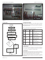
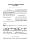
1
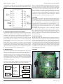
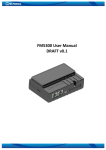
ISSN : 2230-7109 (Online) | ISSN : 2230-9543 (Print)
IJECT Vol. 6, Issue 4, Oct - Dec 2015
IDC cable Test Jig
Abhilash Mudigonda
Dept. of ECE, Vignan University, Guntur, AP, India
Abstract
In Electronics and Electrical Engineering Industry, FRC and IDC
cables play a major role in data transfer. A major challenge lies
in failure of these cables. It could be either loss or excess of data
flow or it could be data corruption due to mishandling or damage
in these lines. This issue may arrive while manually installing
connectors over these cables, and this happens to be a stumbling
block to overcome now a days. As a consequence, a lot of reverse
engineering is being done in order to trace the problem and many
ribbons are being sent back for reinstallation which might cause
wastage of time and even material. So, at least to predict the error
at the installation stage itself would reduce the time wastage and
could also bring out the alertness to install properly. It could be a
better choice to choose a controller based circuit for its flexibility
to test in with many logics.
The objective of IDC cable test jig is to test the functionality
of these FRC and IDC Ribbons using a micro controller circuit
which would provide flexibility to test various bit connectors and
indicate whether installation is done properly.
Outline of the logic:
Giving bit1 to all pins except one pin, that pin is assigned 0. Then
if that pin is shorted with any other pin, the output becomes 0.
Similarly, this operation is iterated for the remaining 64 bits and
outcome is compared with the recorded input sequence.
Keywords
IDC cable, Test Jig, ARM 7 processor, Latches, Multiplexers.
I. Introduction
An Insulation Displacement Cable (IDC), also known as multiwire planar cable (shown in Fig below) is a cable with many
conducting wires travelling parallel to each other on the same flat
plane. It is used very frequently in many electronic devices and
machines for continuous transmission of data.
Because the cable is compatible to all the equipment and flexible
to any atmosphere, the utility of it became common. These
ribbon cables are mainly used in internal peripherals of devices,
computers and much other machinery. The wires of the cable are
closed and protect the data when passed throughit. Each wire of
the cable is independent of other wires though they are attached
together. It consists of two female connectors at both the ends,
through which it can be connected to male connectors of the
device. These ribbons are of various types depending upon the
number of wires attached to each other.
These various types can be use according to our requirement.
In many electronic firms where these cables are used for data
transmission with their end points crimped with connectors.
There are different ways to crimp the connectors over the cables.
Automated crimping and manual crimping.In case, manual
crimping is used, there could be a possibility of error.
II. Problem and Objective
A. Problem
The only problem faced by the user with the IDC ribbon is whenever
the wires of the ribbon gets Short circuit to each other or gets open
68
International Journal of Electronics & Communication Technology
at any place throughout the ribbon, one cannot identify the short
or open without opening the connectors. If the short or open is to
be traced, the user must open the connectors on either side of the
ribbon and manually check the pins for problem. This consumes
the precious time of the user and is also a bit complicated work.
B. Objective
To build a circuit in order to test the functionality of the FRC and
IDC cables, this would predict the error at the installation stage
and reduce the possibility of rework.
III. Initial Design Thought
The risk of verifying the problem in the ribbon manually can be
reduced by using the test jig prepared by me. Using this jig, user
can test the ribbon by just inserting into the male connector of the
jig and can know the type of problem (either short or open) and
also place of problem within no time. The test jig is very simple
to assemble and the cost of making it is very cheap since it is
made with simple components. After experimenting with high
level components to make the testing of IDC cables automatic, we
learnt that this can be made too easy even with basic components.
The material used to make the test circuit is a general purpose
PCB, IC 7486 (XOR gate), resistors (value depends on the voltage
used, but generally need 200 ohms for 5v source) 3 mm. LEDs
and a male connector.
A. Construction
Connector
XOR gate
Resistors
LED Indicators
Fig. 1: Block Diagram Along With Initial Circuit
Here in the test jig, the odd pins of male connector in the circuit
are given logic ‘1’ and evenpins are given logic ‘0’ (here ‘1’
indicates +5v and ‘0’ indicated GND). From the same connector,
pin 1is connected to first pin of IC 7486 and pin 2 is connected
to second pin of IC. Now, the third pin of theIC is connected to
LED via resistor. In the same way, pin 3 of connector is connected
to fourth pin of theIC and pin 4 to fifth pin. Sixth pin of the IC
is connected to LED through a resistor.The basic blockdiagram
is shown in Fig and its soldered circuit is shown in figure. These
connections continuous according to the number of wired ribbon
used. The negative end of the LED will be grounded. Thenumber
of ICs required depends on the number of wires present in the
ribbon.
w w w. i j e c t. o r g
ISSN : 2230-7109 (Online) | ISSN : 2230-9543 (Print)
B. Working
The basic logic behind this circuit can be understood by knowing
the truth table of XOR gate shown. By inserting the female
connector of the ribbon into the male connector of test jig, due
to the connections i.e. logic ‘1’ to odd pins and logic ‘0’ to even
pins, the input of XOR gate appear as ‘1’ and ‘0’ which makes the
output of ‘1’ and makes the LED glow. If there exists any short
or open, the inputs will be either ‘1’ and ‘1’ or ‘0’ and ‘0’, which
makes the output ‘0’ and the LED does not glow. This indication
of the LED not glowing resembles problem in the pins of the
ribbon wires connected to that particular LED via IC.
IJECT Vol. 6, Issue 4, Oct - Dec 2015
purposes. These micro-controllers incorporate a 10/100 Ethernet
MAC, USB 2.0 Full Speed interface, four UARTs, two CAN
channels, an SPI interface, two Synchronous Serial Ports (SSP),
three I2C interfaces, an I2S interface, and a Mini Bus (LPC2378
only: 8-bit data/16-bit address parallel bus).
Fig. 3: ARM7 LPC2368 Micro-controller
Fig. 2: Ex-OR gate and its Truth Table
C. Limitations
1. The major drawback of this circuit is it cannot withstand the
power fluctuations and Vcc load.
2. As the pins get short, Vcc and ground get connected to each
other, eventually the circuit fails and hence its components.
This makes the experiment a complete failure.
3. The other limitation is its complexity. Usage of so many IC’s
increases the complexity andhence the circuit seems bulky.
4. The circuit is also a rigid one. Only, a rigid logic could be
applied and multiple tests cannot be performed.
IV. Micro-Controller based Test Jig
The alternate approach could be usage of a micro-controller driven
circuit. The circuit consists of data directing components such
as latches and multiplexers. The primary idea of the circuit is to
send data to one end of the ribbon and collect the data from other
end back to the controller. The core logic of the test jig lies here.
Because, by sending to and reading back the data status of the
ribbon pins could be easily found out.
The components mainly used in this circuit are:
1. ARM7 (LPC 2368) micro-controller.
2. 74HC 574 latches.
3. 74 HC 151 dual multiplexers.
4. Connecting wires, coupling capacitors (as per
requirement).
A. LPC 2368 ARM7 Micro-controller
LPC2364/6/8/78 is an ARM-based micro-controller for
applications requiring serial communication for a variety of
w w w. i j e c t. o r g
B. 74HC574 Octal D-latch
The M74HC574 is an high speed CMOS octal D-type latch with
3-state outputs inverting fabricated with sub-micron silicon gate
C2MOS technology. This 8 bitD-TYPE FLIP FLOP is controlled
by a clock input (CK) and an output enable input (OE). On
thepositive transition of the clock, the Q outputs will be set to
the logic states that were setup at the D inputs.
While the OE input is at low level, the eight outputs will be
in a normal logic state (high orlow logic level) and while OE
is in high level the outputs will be in a high impedance state.
The outputcontrol does not affect the internal operation of flipflops; that is, the old data can be retained or the newdata can be
entered even while the outputs are off. All inputs are equipped
with protection circuitsagainst static discharge and transient excess
voltage
Fig. 4: 74HC574 Octal Latch Pin Diagram
C. 74 HC151 Dual Multiplexer
The M74HC151 is a high speed CMOS 8 channel multiplexer
fabricated with silicon Gate C2MOS technology. It provides, in
one package, the ability to select one bit of data from up to eight
sources. The M74HC151 can be used as a universal function
generator to generate any logic function of four variables. Outputs
Y and W are complementary; the selection depends on the address
inputs A, B, and C. The strobe input must be taken low to enable
this device, when the strobe is high output is forced high and
International Journal of Electronics & Communication Technology 69
ISSN : 2230-7109 (Online) | ISSN : 2230-9543 (Print)
IJECT Vol. 6, Issue 4, Oct - Dec 2015
consequently Y output goes low. All inputs are equipped with
protection circuits against static discharge and transient excess
voltage.
Fig. 5: 74HC151 8*1 Dual Mux Pin Diagram
D. Testing for 64-pin FRC Connector Ribbon
Giving bit 1 to all pins except one pin, that pin is assigned 0.Then
if that pin is shorted with anyother pin, the output becomes
0.Similarly, this operation is iterated for the remaining 64 bits
and outcome is compared with the recorded input sequence.
For instance, if there is a short between pin 51 and pin 52 and
during iteration bit 0 is applied to pin 51, and then output would
be 0 for both pins. Hence we can say that there is a short between
pins 51and 52.
If there is any error in continuity. i.e., when bit 1 is given to all the
pins and output collected is not the same then continuity could be
predicted. The circuit elements could probably be, Eight 74574
latches for reading the input and nine 8*1 multiplexers connected
to output to read it back to the controller circuit.
E. Design Criteria
The circuit is designed as per the stipulated data flow driven from
the micro-controller card. The micro-controller accesses data from
a 40-pin connector which is a collection of certain port pins.
Utilization of those port pins sums up partial design of the circuit.
The micro-controller is only responsible for accessing the data
and further processing it, the rest of data flow must be controlled
and regulated by the circuit elements. i.e., here the elements are
multiplexers and latches.
Here, we need to send data to 64 latch pins butwe have only 8 port
pins to access. Hence we send the data to the latches commonly
and read from them by varying the clock pins. The construction
of the receiving end is related with the multiplexer set. Here,
eight multiplexers are placed to read the ribbon status and send
back to controller for comparing the output and input. The 64 bits
are redirected to the eight multiplexers and the output of eight
multiplexers is again connected to another multiplexer, and the
final output bit pin is connected to the port pins set.
F. Working
Firstly, when the controller is on, and ribbon is placed, a bit sequence
of 000000FE is passed. i.e., first pin is set 0 and remaining pins
are set 1 and this data is read to the ribbon and clockpins are set
as the same 00000001, i.e., first latch is clock enabled and soon
after that data is set, the latch bits are set with all bit 1’s, i.e.,
000000FF, and next all the remaining latches are clock enabled.
So that first bit is set 0 and remaining 63 bits are set 1 and the
data is accessed.
For example, if input sequence is 1111011, and if the pin bearing
bit0 is shorted with the adjacent pin, the output could be 1110011.
Now, the XOR comparison result would be 0001000. Now the
obtained output is sorted out to find out the faulty pin. Here if
the bit 1 is present in i’th position, then that pin number is said
to be the faulty bit.
G. LCD Panel Circuit
The obtained result is to be displayed on an LCD display. The LCD
display used is a 24*2 LCD panel, which implies that the character
length is 24 and comprises of 2 rows. The LCD panel is interfaced
to the controller through a 26-pin connector. Requirements for
LCD interfacing circuit are a 24*2 character length LCD panel and
a 10K Potentiometer (POT). The condition of the IDC cable would
be displayed on the LCD panel as “Faulty” with corresponding
pin number and type of the fault or if the cable is alright then it
will be displayed as “No fault”.
F. Circuits
The below shown block diagram is in detail explained in the
following circuit block Diagram to test a 64-pin connector.
Power
supply
LCD
Panel
LPC 2368
ARM 7
Controller
card (along
with
peripherals)
74574
Latches
Connector with
IDC ribbon
74HC151
Multiplexers
Fig. 6: Block Schematics for IDC Cable Test Jig
70
International Journal of Electronics & Communication Technology
Fig. 7: LPC 2368 Micro-controller card along with peripherals
w w w. i j e c t. o r g
IJECT Vol. 6, Issue 4, Oct - Dec 2015
ISSN : 2230-7109 (Online) | ISSN : 2230-9543 (Print)
Fig. 8: Latches and Multiplexers Connected as Per Block
Diagram
Fig. 9: Part of Circuit Showing Connectors where the IDC Cable
Needs to be Placed.
H. Flow Chart
I. Testing Observations
The test Jig was tested with various data cables by making
deliberate faults such as shorting two pins and then three pins.
The output was as expected. It was also tested for discontinuity
and got desired results.
Start
Initialize LCD display
Table 1: Observations for IDC Cable Test Jig With Multiple
Combinations of Errors Produced in Cable
Display “Insert IDC cable”
Send Input sequence to the
connector through latches
Read back the data from the other
end through multiplexers
Compare Input and
Output sequences
If Input
sequence =
Output
sequence
Display: “Faulty cable and
error at pin number: Type
of fault: Short/Open
End
w w w. i j e c t. o r g
Type of
Error
No of
bits
1
Open
2
2
Open
3
3
Open
4
4
Short
2
5
Short
3
Yes
Display in LCD
panel: “No
fault present”
No
S.no
Message displayed on LCD
screen
Faulty cable and error at pin
number 41,42
Type of fault: Open
Faulty cable and error at pin
number 52,53,54
Type of fault: Open
Faulty cable and error at pin
number 11,12,13,14
Type of fault: Open
Faulty cable and error at pin
number 12,13
Type of fault: Short
Faulty cable and error at pin
number 24,25,26
Type of fault: Short
J. Future Scope
This test jig can be further modified to suit data cables of different
bits.ie. 32 bit, 16 bit etc. Input devices can also be provided to
give various sets of sequences to the data cables.
V. Conclusion
The proposed system IDC Cable Test Jig is tested successfully by
shorting one bit with another and one bit with all other bits and
also by providing deliberate discontinuity in the cables.
The IDC Cable Test Jig is tested for various combinations of short
and open circuit and it provided expected results for majority of
the scenarios.
International Journal of Electronics & Communication Technology 71
IJECT Vol. 6, Issue 4, Oct - Dec 2015
This test jig is further modified and tested for different buses and
wiring harnesses and got expected results.
References
[1] ARM user development guide
[2] ARM System Development Guide by Andrew Sloss, Dominic
Symes, and Chris Wright.
[3] LPC 23XX user manual-NXP Semiconductors.
[4] C and C++ für Embedded Systems by Friedrich Bollow,
Matthias Homann, Klaus-Peter Köhn
[5] LPC 23XX Data sheet-NXP Semiconductors.
[6] UV4- Getting Started with KEIL-user guide.
72
International Journal of Electronics & Communication Technology
ISSN : 2230-7109 (Online) | ISSN : 2230-9543 (Print)
Abhilash Mudigonda received his
B.tech degree in Electronics and
Communication Engineering from
Vignan University, Guntur, AP, India,
in 2013. He worked as an Intern at
Efftronics Systems Private Limited,
Vijayawada, India. He is currently
working as System Engineer in Tata
Consultancy Services – Engineering
and Industrial Services (TCS-EIS). His
interests include Embedded Systems
especially in the field of Automobiles. He is also interested in
Industrial Automation and Applied Electronics.
w w w. i j e c t. o r g