1
US005963142A
United States Patent [19]
[11] Patent Number:
Zinsky et al.
[45]
[54]
[75]
SECURITY CONTROL FOR PERSONAL
5,313,639
COMPUTER
5,355,414
10/1994 Hale et a1.
5,375,243
12/1994 ParZych et al.
Inventors: Timothy R_ Zinsky, Houston; Charles
N Shaver Cypress, RogerA Kaiser
_
.
.
5,451,934
_
[73] Ass1gnee: Compaq Computer Corporation,
..... .. 380/25
. 395/725
9/1995
Dawson et al. ....... ..
340/82531
340/82531 X
5,533,125
7/1996 Bensimon et al. ................. .. 380/4
5,537,544
7/1996
Houston, Tex
Notice:
5/1994 Chao ................................... .. 380/25 X
5,475,762 12/1995 Morisawa et al. ..
an of TeX_
*Oct. 5, 1999
5,377,343 12/1994 YaeZaWa ............................... .. 380/3 X
5,388,156 2/1995 Blackledge, Jr. et al. ................ .. 380/4
Jr" Paul B‘ Rawhns’ both of smug’
[ * ]
Date of Patent:
5,963,142
Morisawa et al. .... ..
380/25 X
FOREIGN PATENT DOCUMENTS
This patent issued on a Continued pros_
2 154 344
9/1985
United Kingdom ................... .. 380/25
ecution application ?led under 37 CFR
OTHER PUBLICATIONS
1539])’ and 1S Sublect to the twenty year
patent term provisions of 35 U.S.C.
154(a)(2).
COMPAQ DESKPRO/M Reference Guide, pp. 5—1 through
5—13. No Date,
DiskLock Advertisement, PC Magazine, vol. 10, No. 11,
_
Jun. 11, 1991; NeW York, NeW York; p. 139.
[21] Appl' NO" 08/779’061
FastLock User’s Manual, Version 1.0, Rupp Corp., NeW
[22]
York, NeW York. No Date.
Primary Examiner—Brian Zimmerman
Filed:
Jam 6, 1997
Related US. Application Data
[63]
Assistant Examiner—William H. Wilson, Jr.
Attorney, Agent, or Firm—Akin, Gump, Strauss, Hauer &
Continuation of application No. 08/779,061, Jan. 6, 1997,
which is a continuation of application No. 08/398,343, Mar.
Feld’ LLP‘
3, 1995, abandoned.
[57]
[51]
Int. Cl.6 .................................................... .. G06F 12/14
A personal Computer provides Security features enabling
[52]
US‘ Cl‘
control over access to data retained in the computer. The
[58] F M f S
1e
0
earc
L
’
....................... ..
546/825 31 ézs 34
.
,
.
computer is secured by having the system ROM provide a
;
passWord at poWer-on to a security device Which controls
access to the secured features. Once a passWord has been
doWnloaded to the security device, a Protect Resources
380/4, 23, 25, 3, 395/186, 188.01; 711/164,
163; 707/9; 364/70905
,
[56]
ABSTRACT
command is issued to the securit device. To
ain access to
References Clted
the secured feature after boot-Rip, the usergprovides the
Us PATENT DOCUMENTS
correct passWord to the security device and Waits for
approval from the security device. Since the security device
4’942’6O6
?/
llziitrolewicz """"""""""
72990 Kiliseir
4’959’860
9/199O Watters ct a'l '
/
‘380M
""""" " 380M
resources is no longer required, the computer issues another
X
Protect Resources command to the security device to once
5066263 10/1991 BOSCH et aL
5,173,940
5,212,729
5,265,163
12/1992 LantZ et al.
5/1993
only veri?es the passWord and does not divulge it, security
of the system is enhanced. Once access to protected
....... .. 380/25
Schafer ....... ..
more 106k access to the Protected resources
380/4
11/1993 Golding et al. ......................... .. 380/25
81
'i
208
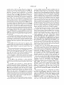
e102 ______ __
cpuuggziiinimonvnm
:
: 214
MD(H..E3)21B
:
DRAM‘:
DATA
:
F144
BUFFEHS
‘I
mt, cAs/
i 05”‘
‘i
:
PRUEESSHR
220 :l
MFM noun, MEMW£
mm]
12 Claims, 12 Drawing Sheets
aaa
cumrmum
F206
HUSTETHUSTATUS
:
_-> CONQEEIELEH
:
]
a
:
:1
____ __210___’]
________________ _
7
wicuwmnum
nms
PAHALlElPURT
n1 BUSlPBI Am wan
j
p
135
HUFPY DUNTHULLER
FUJPPY
DDNTRUL
RTCIEMDS
UARTS
U.S. Patent
0a. 5, 1999
Sheet 2 0f 12
5,963,142
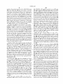
SET
MISMATCH
/ 416
DELAY ONE
,
secomn
ASSERT
UNLOCK_BIT
r 422
PROVIDE STATUS
‘
<_
0F INDEXED SLUT
UPDATE
CMD=STORE
PASSWURD
PAssgvonn
/- 430
DEASSERT
,
UNLOCK_BIT
434
PERMANENTLY
LUCK
FIG. 2
?
U.S. Patent
0a. 5, 1999
Sheet 3 0f 12
5,963,142
RESET
WRITE_CMD &
STORE_PASSWD_CMD
(WRITE_DATA &
PASSWD_CNT=0 &
NOTlSET MISMATCH
[JR MISMATCH» DR
(WR|TE_CMD &
CMD < > READ_STATUS)
& !UNLUCK_
ACE
RESOUECE
STORE
PASSWD
(WR|TE_DATA &
PASSWD_CNT=U) on
(WRITE_CMD &
CMD < > READ_
WRITE-DATA &
STATUS)
PASSWD_CNT=UK
(SET_M|SMATCH 0R MISMATCH)
DELAY_COUNT=@
FIG. 3
U.S. Patent
0a. 5, 1999
Sheet 7 0f 12
560
f- 562
INITIALIZATION
T K568
INITIALIZE
SECURITY
DEVICE
T [564
REOUEST
POWER-ON
PASSWORD
—T—-,566
CONTINUE
POWER ON
SELF TEST
ROUTINES
,}
{-570
LOCK CMOS
MEMORY
572
FIG. 8
5,963,142
U.S. Patent
0a. 5, 1999
Sheet 8 0f 12
5,963,142
586
CALL TO SECURITY
DEVICE
587
CMD=
INITIALIZE
Y
r 589
INITIALIZE
?
N
588
pEgmagK Y
/590
PERM. LOCK
?
N
592
CMD=
Y
PROTECT
ESUURCES
K594
PROTECT
?
N
v
596
CMD==
Y
ACCESS
r598
ACCESS
ESOIgRCES
N
600
SCTWJS
Y
'2
N
504
END
FIG. 9
r602
STATUS
U.S. Patent
0a. 5, 1999
Sheet 9 0f 12
5,963,142
589
INITIALIZE
SECURITY DEVICE
570
IS
CMOS MEMORY
[572
ISSUE STORE
PASSWORD
COMMAND
574
IS
ADMIN.
PASSWORD
576 \
UPDATE
SECURITY DEVICE
WITH DEFAULT
PASSWORD
UPDATE
SECURITY DEVICE
WITH ADMIN.
PASSWORD
*I
580
ENABLE FLASH
ROM PROTECT
l
I
/582
ISSUE PROTECT
RESOURCES CMD
TO SECURITY
DEVICE
584
FIG. 10
U.S. Patent
0a. 5, 1999
Sheet 10 0f 12
590
PERM LOCK
K606
WRITE FLASH
ROM LOCK
VALUE TO
REGISTER
I [608
SEND COMMAND
TO LOCK
RESOURCES TO
SECURITY DEVICE
% 5610
FIG. 11
594
r612
WRITE FLASH
ROM PROTECT
VALVE TO
REGISTER
I,
(614
SEND COMMAND
TO PROTECT
RESOURCES TO
SECURITY DEVICE
% 3-616
FIG. 12
5,963,142
U.S. Patent
0a. 5, 1999
Sheet 11 0f 12
5,963,142
598
618
CUNFIG
CMDS MEMORY
LOCKED
T
'
626
SEND COMMAND
TO ACCESS
RESOURCES T0
SECURITY DEVICE
VALID cmos.
PASSgVURD
628\
)I
PERIIRYTRRM
usER
n
/
F 638
SEND COMMAND T0
WAIT ONE
ACCESS RETsouRvcEs
¢
T0 sEcuRI Y DE ICE
I
WRITE BYTE To
624
630
SECOND
SECURITY DEVICE
SEND DEFAULT
PASSWORD
SECURITY
DEVICE STATUS
641 \
=UNL5JCKED
SET FAILED
FLAG
/
R M NL I:
WSIITEFLGSE
VALUE T0
644
INDICATE
FAILURE
*
REGISTER
646
FIG. 13
U.S. Patent
0a. 5, 1999
5,963,142
Sheet 12 0f 12
602
f 650
SENT READ
STATUS
COMMAND TO
SECURITY DEVICE
I
f- 652
READ DATA PORT
OF SECURITY
DEVICE TO GET
STATUS
% 5-654
FIG. 14
676
678
ISSUE ACCESS
RESOURCES
COMMAND TO BIOS
HANDLER
/ 682
INDICATE
FAILURE
ACCESS
RESOURCES AS
DESIRED
I
f 688
ISSUE PROTECT
RESOURCES
COMMAND TO
BIOS HANDLER
690
FIG. 15
5,963,142
1
2
SECURITY CONTROL FOR PERSONAL
COMPUTER
sary level of security. But at the same time, the passWord
approach must be suf?ciently secure so that the passWord
cannot be obtained during the process. Thus, a security
device is needed that can verify a passWord provided by the
This is a continuation of co-pending application Ser. No.
08/779,061 ?led on Jan. 6, 1997 and abandoned Ser. No.
08/398,343, ?led on Mar. 3, 1995.
user instead of requiring the user to throW a sWitch to update
the ?ash ROM and to perform such veri?cation in a secure
manner.
BACKGROUND OF THE INVENTION
SUMMARY OF THE INVENTION
1. Field of the Invention
10
This invention relates to personal computer systems and,
more particularly, to a personal computer having security
A computer according to the present invention provides
security by having the system ROM provide a passWord at
features enabling control over access to data retained in the
poWer-on to a security device Which controls access to the
computer.
secured features. Once a passWord has been doWnloaded to
the security device, a Protect Resources command is issued
to the security device Which controls access to the protected
2. Description of the Related Art
15
The rapid development and adaptation of neW technology
in the computer industry has enabled personal computers
resources such as the ?ash ROM. To access the secured
resource, the user provides the correct passWord to the
and peripherals to become ever more poWerful and sophis
ticated. HoWever, the torrid pace of technological innovation
has rendered many otherWise operable personal computers
20
These and other features of the present invention Will be
obsolete due to outdated system softWare. Particularly, if the
system resident code (or ?rmware) is outdated, an IBM
compatible computer may not be able to support features
available With the latest peripherals.
Developed since the earliest generation of personal
computers, the ?rmware residing in read only memory
security device. The security device can only verify and not
divulge the passWord, so security of the system is enhanced.
understood upon reading of the folloWing description along
With the draWings.
BRIEF DESCRIPTION OF THE DRAWINGS
25
A better understanding of the present invention can be
obtained When the folloWing detailed description of the
preferred embodiment is considered in conjunction With the
(ROM) provides an operational interface betWeen a user’s
application program/operating system and the device to
relieve the user of the concern about speci?c characteristics
folloWing draWings, in Which:
of hardWare devices. This insulation layer of code eventually
evolved into a Basic Input/Output System (BIOS) code
FIG. 1 is a block diagram of a computer system according
to the present invention;
FIG. 2 is How diagram of the security management system
in accordance With the present invention;
Which alloWed neW devices to be added to the system While
isolating the application program from the peculiarities of
the hardWare. Since the BIOS is an integral part of the
system and controls the movement of data in and out of the
35
system processor, it resides on the system ROM. As neW
FIGS. 4, 5 and 6 are schematic diagrams of portions of the
security management system associated With the state
machine of FIG. 4;
models of the personal computer family are introduced, the
BIOS had to be updated and expanded to include neW
hardWare and I/O devices.
Since the technology is rapidly changing and neW I/O
devices are being added to the personal computer systems,
40
FIG. 8 is a How chart of the boot-up process of the
modi?cation to the BIOS and other system softWare is
has made possible the ability to update the contents of the
ROM Without ever physically removing the ROM.
HoWever, since the BIOS is an integral part of the operating
system, a corrupt BIOS could lead to devastating results and
in many cases to complete failure and non-operation of the
computer of FIG. 1;
45
FIG. 10 is a How chart of BIOS initialiZation of the
security management system in accordance With the inven
50
FIG. 11 is a How chart of the BIOS softWare handler for
55
publicity on the adverse consequences of computer security
breaches. Thus, security conscious users are requesting that
security and integrity features be incorporated into their
60
issuing commands in general to the security management
updating of the ?ash ROM. HoWever, the sWitch method
Was burdensome and in?exible. A passWord approach is
enhanced user convenience While still providing the neces
the read status command of FIG. 10; and
FIG. 15 is an illustrative ?oW chart of the softWare for
system in accordance With the invention.
In previous systems, a sWitch Was used to control the
desirable due to loWer cost of eliminating a sWitch, increased
FIG. 12 is a How chart of the BIOS softWare handler for
the protect resources command of FIG. 10;
FIG. 13 is a How chart of the BIOS softWare handler for
the access resources command of FIG. 10;
FIG. 14 is a How chart of the BIOS softWare handler for
personal computers to protect the ?ash ROM and to prevent
?exibility because passWords can be easily changed, and
tion;
the permanent lock command of FIG. 10;
The user’s aWareness of accidental or intentional misuse
unintentional or malicious erasure of the ?ash ROM con
tents.
FIG. 9 is a How chart of the BIOS softWare handler for the
security management system in accordance With the inven
tion;
system.
or otherWise unauthoriZed modi?cations to the computer’s
system softWare has been made more acute folloWing the
FIG. 7 is a schematic diagram of the ?ash ROM pro
gramming circuit;
desirable to keep existing personal computers up to date to
support the latest peripherals While maintaining compatibil
ity With existing peripherals. The availability of ?ash ROMs
FIG. 3 is a state machine of the security management
system used in implementing the How diagram of FIG. 2;
65
DETAILED DESCRIPTION OF THE
PREFERRED EMBODIMENT
Prior to discussing FIGS. 2—15 Which detail the security
management system in accordance With the present
5,963,142
3
4
invention, a general background summary of the operation
of the personal computer protected by the security manage
provided on the system S and are connected to ?lter and
transformer circuitry 126, Which in turn is connected to the
ment system of the present invention merits revieW.
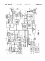
Referring noW to FIG. 1, a computer system S according
to the present invention is shoWn. In the preferred
embodiment, there are tWo primary buses located in the
system S. The ?rst bus is the PCI or Peripheral Component
Interconnect bus P Which includes an address/data portion
controller 120. This forms a netWork or Ethernet connection
for connecting the computer system S to a local area netWork
(LAN).
A PCI-ISA bridge 130 is provided to convert signals
betWeen the PCI bus P and the ISA bus I. The PCI-ISA
bridge 130 includes the necessary address and data buffers
and control signal portion. The second primary bus in the
system S is the ISA bus I. The ISA bus I includes an address
and latches, arbitration and bus master control logic for the
10
portion, a data portion 110, and a control signal portion 112.
conventionally used in ISA systems, an IDE (integrated
drive electronics) interface, and a DMA controller. Prefer
The PCI and ISA buses P and I form the backbones of the
system S.
A CPU/memory subsystem 100 is connected to the PCI
bus P. The processor 200 is preferably the Pentium processor
from Intel, preferably operating externally at 50 or 60 MHZ,
ably the PCI-ISA bridge 130 is a single integrated circuit,
15
but could be an 80486 from Intel or processors compatible
With the 80486 or Pentium or other processors if desired.
The processor 200 provides data, address, and control por
tions 202, 204, 206 to form a host bus HB. A level 2
or
external cache memory system 208 is connected to the host
20
bus HB to provide additional caching capabilities to improve
performance of the computer system. The L2 cache 208 may
25
as the 82434X chip from Intel Corporation or the chip
described in patent applications Ser. Nos. 08/324,016,
a cable to a ?oppy disk drive is connected to the combination
30
Intel, or those described in patent applications Ser. Nos.
08/324,246 now US. Pat. 5,634,073 as incorporated above
and 08/323,263 entitled “DATA ERROR DETECTION
AND CORRECTION SYSTEM”, ?led Oct. 14, 1994, now
35
turn to a keyboard connector 158 and a mouse or pointing
40
45
132 includes circuitry of a security management system
50
?ash ROM 154 through Write protection logic 540.
art.
55
Turning to FIG. 2, the operation of the security device is
provided in greater detail as a ?oWchart. The preferred
embodiment of the security device comprises the folloWing
60
connector 308 is connected to the RAMDAC 306. Amonitor
act as a PCI bus master and slave and the circuitry to act as
an Ethernet interface. Alternate Ethernet connectors 124 are
according to the present invention and so is connected to the
This is an exemplary computer system S and other
variations could readily be developed by one skilled in the
signal bus 220 is provided from the bridge chip 210.
(not shoWn) is connected to the video connector 308.
A netWork interface controller (NIC) 120 is connected to
the PCI bus P. Preferably the controller 120 is a single
integrated circuit and includes the capabilities necessary to
Amiscellaneous system logic chip 132 is connected to the
X bus X. The miscellaneous system logic chip 132 contains
counters and timers as conventionally present in personal
computer systems, an interrupt controller for both the PCI
and ISA buses P and I, enhanced parallel port circuitry and
circuitry. Additionally, the miscellaneous system logic chip
to the PCI bus P for data transfer over that bus. The data
buffers 212 provide a memory data bus 218 to the memory
array 214, While a memory address and memory control
analog converter (RAMDAC) 306. The video graphics con
troller 300 controls the operation of the video memory 304,
alloWing data to be Written and retrieved as required. Avideo
device connector 160.
poWer management logic, as Well as other miscellaneous
reference, and are utiliZed to handle memory data to a main
memory array 214. The data buffers 212 are connected to the
A video controller 300 is connected to the PCI bus P.
Video memory 304 is used to store the graphics data and is
connected to the video graphics controller 300 and a digital/
can be reprogrammed to alloW for revisions of the BIOS. An
8042 or keyboard controller 156 is connected to the X bus
X and ISA bus I address and control portion. The keyboard
controller 156 is of conventional design and is connected in
US. Pat. No. 5,555,250 and hereby incorporated by
processor data portion 202 and receive control signals from
the bridge chip 210. The data buffers 212 are also connected
144 is connected to the ISA bus I to provide an additional X
bus X for various additional components of the computer
system. A ?ash ROM 154 receives its control, address and
data signals from the X bus X. Preferably the ?ash ROM 154
contains the BIOS information for the computer system and
connected to the L2 cache 208 as it incorporates the cache
controller and therefore controls the operation of the cache
memory devices in the L2 cache 208. The bridge chip 210
is also connected to control a series of data buffers 212. The
data buffers 212 are preferably similar to the 82433LX from
control access to the CMOS memory and the poWer on
I/O chip 136 and the ISA bus I. Serial port connectors 137
are also connected to the combination I/O chip 136. Abuffer
MEMORY” pending and 08/324,246, entitled “SYSTEM
14, 1994, now US. Pat. No. 5,634,073, and hereby incor
porated by reference, is connected to the control portion 206
and to the address portion 204. The bridge chip 210 is
UARTs, various address decode logic and security logic to
passWord values. A ?oppy disk connector 138 for receiving
entitled “SINGLE BANK, MULTIPLE WAY CACHE
HAVING A PLURALITY OF POSTING QUEUES ASSO
CIATED WITH DIFFERENT TYPES OF WRITE OPERA
TIONS FOR SELECTIVELY CHECKING ONE QUEUE
BASED UPON TYPE OR READ OPERATION”, ?led Oct.
but other combinations are possible. A series of ISA slots
134 are connected to the ISA bus I to receive ISA adapter
cards. Aseries of IDE slots 133 are connected to the ISA bus
I and the PCI-ISA bridge chip 130 to receive various IDE
devices, such as hard disk drives, tape drives and CD-ROM
drives. Aseries of PCI slots 135 are connected to the PCI bus
P to receive PCI adapter cards.
A combination I/O chip 136 is connected to the ISA bus
I. The combination I/ O chip 136 preferably includes a ?oppy
disk controller, real time clock (RTC), CMOS memory, tWo
be permanently installed or may be removable if desired. A
cache and memory controller and PCI bridge chip 210, such
PCI bus, ISA arbitration circuitry, an ISA bus controller as
elements: a command register and decoder for the security
device; a data/status register for communicating With the
computer, an eight byte register ?le to store passWord for
each of the protected resources, and passWord veri?cation
logic.
65
Commands are preferably issued from the computer to the
security device at a predetermined address. Status may be
read from the last resource, or slot, indexed. The security
device is capable of protecting a plurality of resources or
slots. In the preferred embodiment shoWn in detail, only a
5,963,142
5
6
single resource is protected, but at various locations refer
-continued
ence is explicitly made to the plurality of resources or slots
Commands
and those skilled in the art can readily determine appropriate
modi?cations where not speci?cally discussed. A Read
Status command is con?gured so that the status register of
any particular resource, or slot, can be read, without affect
ing other operations occurring to a resource or slot, such as
unlocking or changing a password. Access to a speci?c
resource, or slot, in the security device is performed with an
indexed address scheme. Two addresses are used for the
Black Box
Command
Command
Code
Command Description
making changes so that the resource is
once again protected.
Permanently X8H
Permantently lock all resources. Future
Lock
accesses to protected system resources
10 Resources
are not possible unless power is cycled.
A status register read is possible.
indexing scheme, one address is for commands, while the
second address is the data/status register. The second address
acts as a data register for a write cycle and as a status register
during a read cycle. The index is placed in the upper three
bits of the command register.
The format of the command register of the preferred
15
In addition to sending commands to the security device,
status can be read from the security device at any time, by
reading the status/data register, preferably located at a sec
ond predetermined address adjacent to the ?rst predeter
embodiment is as follows:
mined address. The data/status register serves two purposes.
When serving as the data register, the register is used when
storing passwords or verifying passwords (accessing
Read or
Bit(s)
resources).
Write Name
Description
7-5
R/W
IDX[2:O]
Slot index which point to a
4
R/W
Reserved
particular resource, or slot
Reserved bit
3-0
R/W CMD[3:O]
To store passwords, the Store Password command must
?rst be sent to the security device. Then, the next eight writes
Command bits executed by security
device
to the data/status register cause the data written to the
data/status register to be stored as the password for the
25
security device. Eight bytes are preferably written to the
data/status register in the preferred embodiment, although
the actual siZe of the data/status register may be smaller or
greater. If another command for the security device arrives
The slot index, or resource index, encoding for the
preferred embodiment is as follows:
before all eight bytes have been stored for the password, the
password storage operation for that slot in the security
device aborts and the password then contains unde?ned
Slot Index Encoding
Index Bits
Slot
IDXZ
IDX1
IDXO
Number
0
O
O
O
1
1
1
1
O
O
1
1
O
O
1
1
O
1
O
1
O
1
O
1
O
1
2
3
4
5
6
7
35
Commands
BITS
As can be seen, the preferred embodiment allows up to 45
eight slots, or resources, to be controlled by the security
device. Bits 0-3 of the preferred embodiment contain the
command sent to the security device which is encoded as
follows:
Command
Command
Code
Command Description
Read Status
XOH
Changes index pointer to the slots so that a
55
X1H
Protect
XZH
Receives the next eight bytes written to the
data/status port and updates as the new pass
word.
Enables guarding by the security device after
Resources
storing a password or after access to a se
Access
cured resource is completed.
Once this command is given, the next eight
bytes written to the data/status port are com
Resources
X4H
7-5
R
IDX[2:O]
Slot index bits
4-3
R
Reserved
Reserved bits
2
1
R
R
PL
D
0
R
U
Permanently Locked
Delay in progress if set due to mis
match
UNLOCKiPin state
For overview purposes, the simpli?ed operation of the
status register to be compared against a byte of the password
stored in the security device. If correct password is provided,
the resource is unlocked, otherwise the security device is
unavailable for one second before the next command can be
pared against the stored password. If the com
pare is good, the security device will unlock
the resource and allow changes. A Protect Re
sources command must be given when done
DESCRIPTION
security device after initialiZation is next discussed. To
verify a password, ?rst an Access Resources command must
be sent to the security device. Then, the next eight writes to
the data/status register cause the byte written to the data/
status read can occur from another slot.
Store a
Password
READ OR
WRITE
NAME
Bits 7-5 provide an indication of which particular
resource or slot the remaining bits identify. The PL bit
indicates when set that this resource is permanently locked.
The D bit indicates when set that a one second delay is in
progress due to a password mismatch. The U bit is the state
of the UNLOCKi pin or signal for the resource.
Commands
Black Box
data.
The status register provides status information on a par
ticular resource when read. The status register is de?ned
below.
sent.
65
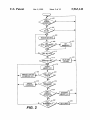
Turning to FIG. 2, the general process of unlocking a slot
after initialiZation is shown. In step 402 a determination is
made if an Access Resources command is received by the
5,963,142
7
8
security device. Until an Access Resource command is
to have multiple resources located in multiple slots for
passWords in the security device. This is done by the use of
the different indeX values, each referencing a different
resource or slot. In this description, the indeX value is alWays
received, the operation essentially loops at step 402. The
resources have to have been protected by the Protect
Resources command during initialiZation as described
beloW in order for the Access Resources command to be
recogniZed. Then in step 404, a determination is made if a
permanent lock resources (PLR) bit has been set to check the
condition that a permanently lock resources command has
been issued. If so, the Access Resources command is
ignored. Once the Access Resources command has been
received and the resource or slot is not permanently locked,
the security device receive a byte representative of a key or
assumed to be Zero to access the ?rst slot. Thus, in a multiple
resource embodiment, there are a plurality of eight byte
passWord registers used to store passWords. In the multiple
10
passWord Written to the data/status port at step 406. The byte
is compared against the appropriate byte in the passWord
stored in the register ?le in the security device at step 408.
Bytes Written to the data/status register are received in the
15
20
byte, a MISMATCH bit is set at step 410. The comparison
sequence is repeated at step 412 until the last byte, or the
25
DETECTION METHOD AND APPARATUS” now US.
Pat. No. 5,537,540 and in US. application Ser. No. 08/231,
30
codes are never visible to the user, this section may perma
35
occur.
states of the machine are sequenced on the falling edge of a
Write instruction to the command register. As shoWn in FIG.
40
then in step 422 the security unit enables the status register
4, the state machine has an IDLE state 440, an ACCi
RESOURCE state 442 in Which access to a secured resource
loW or active in step 418. The UNLOCKi signal is used to
signal that the access to the secured resources has been
granted and is used to enable the secured resources.
If the command is a Read Status command in step 420,
nently locked by the security device.
Turning to FIG. 3, a state machine 438 controlling the
security device according to the invention is disclosed. The
before another attempt to access the security device can
Further, the security unit asserts the UNLOCKi bit signal
443 entitled “METHOD AND APPARATUS FOR ASSESS
ING INTEGRITY OF COMPUTER SOFTWARE”, now
US. Pat. No. 5,421,006 both of Which are hereby incorpo
rated by reference. The Safe Start hash codes could also be
protected by a slot in the security device. Since these hash
In step 414 after the last byte has been received, if the
mismatch ?ag is set, control proceeds to step 416 Where the
Once the Access Resources command has been validated,
the security unit responds to the commands given to it.
partition of the computer. This system is disclosed in US.
patent application Ser. No. 08/315,702 entitled
“TRANSPARENT, SECURE COMPUTER VIRUS
ignored.
unlock output is kept inactive and a one-second delay occurs
of computer data for effects of computer viruses. The Safe
Start system provides veri?cation independent of and trans
parent to the operating system because it uses a reserved
non-DOS hard disk partition system to check on the DOS
eighth byte in the preferred embodiment, has been checked.
The status register is not updated until all eight bytes have
is expecting to receive bytes to compare against the stored
passWord, the passWord veri?cation phase is aborted and the
command that Was received by the security device is
slot may be used to address the rest of the protected areas
Further, Safe Start codes resource is another candidate.
The Safe Start hash codes are used to verify the integrity
After a byte is received, a compare betWeen the received key
been received.
In the preferred embodiment, eight compares must occur
before the result of the veri?cation is checked. If a command
is Written to the command register When the security device
poWer-on passWord slot controls the poWer-on passWord,
Which is currently only changeable at boot time. If a slot is
provided then the poWer-on passWord can be changed at
run-time. In addition to the poWer-on passWord slot, another
that are accessible through the Administrator passWord.
same order as received in the Store PassWord command.
byte and the corresponding byte in the passWord register ?le
is performed. If the key byte fails to match the passWord
resource embodiment, the security device has an UNLOCK_
output for each slot. The additional slots in the security
device can include slots for poWer-on passWord, adminis
trator passWord, Safe Start hash codes, among others. The
may be granted, a STOREiPASSWD state 444 in Which a
neW passWord can be stored, and a DELAY state 446 for
45
delaying responses for a period of time, preferably one
second, if the key provided does not match the passWord.
Upon reset, the state machine 438 is in IDLE state 440. In
this state, only commands are accepted. The IDLE state 440
of the indeXed slot to return the status of that slot back to the
computer.
transitions to the ACCiRESOURCE state 442 When a
In step 424, if the command is a Store PassWord
command is Written to the command register (WRITEi
command, the neXt eight bytes Written to the data/status port
COM), this command is an access resource request (ACCi
RESiCMD), the locked or unlocked status signal
(UNLOCKi) is deasserted or high and the lock status signal
(PLOCKiSTAT) is not asserted. The PLOCKiSTAT
signal, if not asserted, indicates that the Permanent
are to be stored as the neW passWord and this is done in step
426.
In step 428, if the command is a Protect Resources
command, the security feature is restarted such that a neW
passWord veri?cation is required. The UNLOCKi output is
55
deasserted or set high after receiving this command in step
430. Once this command is given, the only Way to change
transition back to the IDLE state 440 or to the DELAY state
446.
The transition from the ACCiRESOURCE state 442 to
security device protected resources is to reissue an Access
Resources command and reprovide the passWord. In step
432, if the user issues a Permanently Lock resources
60
command, the PLR bit is set in step 434. If this command is
Written to the security device, the resources are permanently
locked. Security device access to protected system resources
is no longer possible unless poWer is cycled. HoWever, a
status register read is still possible.
For simplicity, While this description focuses on protect
ing only one resource, it is Within the scope of the invention
Resources command has not been issued. Once in the
ACCiRESOURCE state 442, the state machine 438 may
the IDLE state 440 occurs When data is Written to the
data/status register (WRITEiDATA); the passWord count
equals Zero (PASSWDiCNT=0), indicating that all eight
bytes have just been Written; and the SETiMISMATCH and
MISMATCH signals are deasserted. The SETi
65
MISMATCH signal is set When the current byte being
Written is a mismatch, While the MISMATCH signal indi
cates that a byte previously Written on this attempt mis
5,963,142
10
state 442 to the DELAY state 446 occurs When data is
ENiPASSWDiCNT signal is asserted via an AND gate
474 and the OR gate 470. Further, the output of the AND
gate 474 is ANDed via AND gate 476 With the output of a
comparator 482 Which compares the proper byte in a pass
Word register 478 With a key register 480 to generate the
Written to the data/status register (WRITEiDATA); the
passWord count equals Zero, indicating the last byte has been
SETiMISMATCH signal. The passWord register 478 is
actually the depth of the passWord, eight bytes in the
matched. The transition from the ACCiRESOURCE state
442 to the IDLE state 440 also occurs When a command
other than a Read Status command is Written to the com
mand register. The transition from the ACCiRESOURCE
Written; and either the SETiMISMATCH or the MIS
MATCH signal is asserted. This transition handles the event
Where the key and the passWord do not match. A delay of
10
preferably one second is encountered once the DELAY state
preferred embodiment, and the proper byte is selected based
on the passWord counter 528 value. The key register 480
need only be a single byte register as the previous bytes of
the key need not be stored. The SETiMISMATCH signal
indicates a mismatch of the current byte and is latched to
indicate that a mismatch has already occurred in a previous
446 is entered. This period is clocked by a count-doWn
counter 536 (FIG. 5) Whose output is DELAYiCOUNT.
Thus, upon DELAYiCOUNT reaching Zero, the DELAY
clock period. The output of the latching operation, the
state 446 transitions back to the IDLE state 440.
15 MISMATCH signal, is gated With the SETiMISMATCH
signal using a NOR gate 484. The output of the NOR gate
The IDLE state 440 can also transition to the STOREi
484 is ANDed With the output of the AND gate 474 and the
PASSWD state 444 When a request to the command register
PASSWDiCNT=0 signal by an AND gate 486 to generate
the CLRiPROT signal. The output of the NOR gate 484 is
further inverted by an inverter 490 and then gated With the
output of the AND gate 474 and the PASSWDiCNT=0
signal by an AND gate 492 to generate the delay signals
SETiDLY and SETiDLYiCNT.
(WRITEiCOM) to update the passWord (STOREi
PASSWDiCMD) is Written and the unlocked status signal
(UNLOCKi) is asserted or loW. The STOREiPASSWD
state 444 transitions back to the IDLE state 440 When the
data is Written to the data register (WRITEiDATA) and the
passWord count equals Zero (PASSWDiCNT=0), signify
ing that the last byte of the neW passWord have been
accepted. The STOREiPASSWD state 444 also transitions
25
back to the IDLE state 440 When the When any command
When the state machine 438 is in state ACCi
RESOURCE 442, a command signal is Written to the
command register and the command is Read Status, an AND
gate 494 generates the LATCH STATUS signal via the OR
gate 500. The LATCH STATUS signal is also generated by
other than read status (READiSTATUS) is asserted before
the neW passWord is doWnloaded. Hence, if a command is
sent before all passWord bytes are sent, the state machine
438 transitions back to the IDLE state 440 With the passWord
AND gates 496 and 498 When the state machine is in the
being only partially updated. It should be assumed that the
passWord contains unknoWn values.
delay signal CLR DLY is generated by ANDing the DLYi
DELAY state 446, the Write command signal (WRITEi
CMD) is asserted and the command is Read Status. The clear
CNT=0 signal With the STATE=Delay condition in an AND
Turning to FIGS. 4, 5, and 6, the logic providing the
signals to the state machine 438 is disclosed in more detail.
When the state is the IDLE state 440 and a Read Status 35
command is encountered, a LATCH STATUS signal is
asserted via an AND gate 450 in conjunction With an OR
gate 500. When the state is IDLE, the command is Store
PassWord and the UNLOCKi signal is asserted loW, an
AND gate 452 in conjunction With an OR gate 454 asserts
45
MISMATCH) signal.
In IDLE state 440, When the command is Protect
command is Permanent Lock (PERMANENTiLO CK). The
output of the AND gate 466 is also the SETiPLOCK signal.
In the STORE PASSWD state 444, When data is Written
to the data register (WRITEiDATA), an AND gate 468
asserts the SETiPASSWD signal and the ENiPASSWDi
CNT signal is asserted through an OR gate 470. Further,
When in state STOREiPASSWD, and the Read Status
command is Written to the command register, the LATCH
STATUS signal is asserted via an AND gate 472 and the OR
gate 500.
When the state machine 438 is in state ACCi
RESOURCE 442 and data is Written to the data register, the
preferably the OSC or oscillator signal from the ISA bus I
but could be any suitable clock signal. As shoWn in FIG. 5,
the clear protect signal CLRiPROT is inverted by an
inverter 502 and then ANDed With the output of the ?ip-?op
506 by an AND gate 504 Whose output is provided to an OR
gate 505 Which also receives the set protect signal SETi
PROT and provides its output to the D input of the ?ip-?op
506. In this manner, the ?ip-?op 506 generates the
UNLOCKi signal during the neXt clock transition and is
made active by issuing a PROTECT RESOURCES com
mand or a PERMANENTLY LOCK RESOURCE command
Resource (PROTiRESOURCE) and the UNLOCKi signal
is asserted, the SETiPROT signal is asserted via an AND
gate 458 in conjunction With an OR gate 460. The SETi
PROT signal is also asserted by the OR gate 460 based on
an input from an AND gate 466, Which asserts its output
When the state is IDLE, UNLOCKi is asserted loW, and the
514, 520, and 522 have a clear input Which is tied to the
signal for resetting the computer (RESETi) and a clock
input Which is tied to the clock signal CLK, Which is
the SETiPASSWDiCNT signal. The SETiPASSWDi
CNT signal of the OR gate 454 is also asserted by an AND
gate 464 When the state is IDLE, the UNLOCKi signal is
deasserted or high, the lock status bit (PLOCKiSTAT) is
false, and the command is Access Resource. The output from
the AND gate 464 is also the clear mismatch (CLRi
gate 504.
Turning to FIG. 5, each of a series of ?ip-?ops 506, 508,
to the security device.
The PLOCKiSTAT signal is generated by the ?ip-?op
508, Which receives the output of an OR gate 507 at its D
input and updates the PLOCKiSTAT signal during the neXt
clock CLK transition. The OR gate 507 receives the SETi
55
PLOCK signal and the output of the ?ip-?op 508. The delay
status signal CLRiDLY is inverted by an inverter 510 and
then ANDed With the output of the ?ip-?op 514 via an AND
gate 512 Which provides its output to an OR gate 513 Which
also receives the SETiDLY signal and provides its output
to the D input of the ?ip-?op 514. In this manner, the
?ip-?op 514 generates the DLYiSTAT signal during the
neXt clock transition. Similarly, the clear mismatch signal
65
CLRiMISMAT CH is inverted by an inverter 516 and then
ANDed With the output of the ?ip-?op 520 via an AND gate
518 Which provides its output to an OR gate 519 Which also
receives the SETiMISMATCH signal and provides its
output to the D input of the ?ip-?op 520. In this manner, the
5,963,142
11
12
?ip-?op 520 generates the MISMATCH signal during the
conventional chip select, output enable, and Write enable
next clock transition. The ENiPASSWDiCNT signal is
held by the ?ip-?op 522 one clock period to generate the
DLYiENiPASSWDiCNT to provide additional time for
the other circuits that depend on this signal.
inputs that are driven by circuitry on the computer system S
When the ?ash ROM 164 is addressed. Once the FRWPi
signal is true, the ?ash ROM 164 can be Written in a manner
similar to a random access memory
Thus, the
updating of the ?ash ROM 164 can be accomplished in a
TWo counters 528 and 536 are used to sequence the
passWord count and the delay count, respectively. Both
secure manner.
counters 528 and 536 have the data inputs connected to logic
high, or 5V DC, and the COUNT UP/DOWNi input Wired
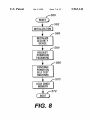
Turning to FIG. 8, a very simpli?ed ?oW chart of the
boot-up process of the computer is disclosed. As shoWn in
FIG. 8, after the computer system S is reset in step 560, the
computer system S is initialiZed in step 562. After this
initialiZation and beginning of certain self test operations. In
to ground to indicate that the counters 528 and 536 are to
10
count doWn. The SETiPASSWDiCNT signal is inverted
by an inverter 524 and then ANDed With the RESETi signal
step 568, the security device is initialiZed. Next, at step 564,
via an AND gate 526, Which drives the inverted load or LDi
signal of the counter 528 to reload the counter 528.
Similarly, the ENiDLYiCNT signal is inverted by an
inverter 532 and then ANDed With the RESETi signal via
an AND gate 534 Which drives the LDi input of the counter
536. The detection that the output of each of counters 528
and 536 equals Zero is performed by an OR gate. Thus, an
OR gate 530 is connected to the outputs of counter 528 to
15
locked in step 570 so that any contained passWords, such as
the poWer-on and administrator passWords, and any Saf
eStart hash codes are secured and cannot be read. This
locking of the CMOS memory is conventional and the
20
generate the PASSWDiCNT=0 signal. Similarly, an OR
gate 538 is connected to the outputs of counter 536 to
provided in Ser. No. 08/315,702, referenced above, but
further information can be obtained in data sheets and
25
signal for resetting purposes. Further, the ?ip-?op 539 is
clocked by the falling edge of a Write protect register address
decode signal. A Write protect register Was provided in the
FIG. 9 is a ?oW chart of the BIOS softWare handler for the
tion. It is noted that in this description all of the index values
in the commands are set to Zero as only a single slot is
30
35
40
45
Write to the ?ash ROM, the ?ash ROM resource must be
unlocked using the security device and the bit in the Write
protect register must be set.
Turning noW to FIG. 7, the Write protect logic 540 is
disclosed. The ?ash ROM Write protect (FRWPi signal and
voltage terminal of the ?ash ROM 154. The programming
voltage terminal of the ?ash ROM 154 is also pulled-up to
logic high through a resistor 554. A pull-up resistor 556 is
further provided to the Write enable input of device 154.
In addition to the connection from the Write protection
logic 540, the ?ash ROM 164 has address inputs Which are
coupled to the address portion of the X bus X, data signals
Which are coupled to the data portion of the X bus X, and
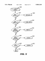
softWare begins When a system call is made to the security
device handler in step 586. The command is then parsed in
steps 587—600. In step 587, if the command is InitialiZe, as
provided in step 568, the InitialiZe routine is executed at step
589. OtherWise, in step 588, if the command is Permanent
Lock, the Perm Lock routine is executed at step 590.
OtherWise, in step 592, if the command is Protect Resources,
the Protect routine is executed at step 594. OtherWise, in step
596, if the command is Access Resources, the Access routine
is executed at step 598. OtherWise, in step 600, if the
command is Read Status, the Status routine is executed at
step 602. OtherWise, the softWare exits at step 604.
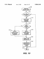
Turning to FIG. 10, the ?oW chart of BIOS initialiZation
routine of the security management system in accordance
With the invention is disclosed. As noted in FIG. 9, the
operation is entered during the poWer up procedures When
the BIOS handler is called With an INITIALIZATION
50
a synchroniZed poWer supply good (SPWRGOOD) signal
are provided to an AND gate 542, Whose output is negated
by an inverter 544 before passing through a buffer 546. A 12
VDC poWer supply is coupled to the output of the buffer 546
via a resistor 548. The output of the buffer 546 is also
provided to a resistor 550, Which is connected to the base of
a PNP transistor 552. The emitter of the transistor 552 is
connected to the 12 VDC poWer supply, While the collector
of the transistor 552 is connected to the programming
present on the preferred embodiment. The index value
Would be properly set based on the resource to be referenced
if several resources Were being secured. The execution of the
combination I/O chip 136 and Was used to enable or disable
protection of the ?ash ROM in prior systems. The use of the
bit in the register is maintained in the preferred embodiment
and is supplemented by the use of the security device to
alloW further protection of the ?ash ROM. To guarantee that
the ?ash ROM is properly protected, that register is mirrored
in the miscellaneous system logic chip 132. The Write
protect register address decode signal indicates a Write to
that register. The output of the ?ip-?op 439 is an FRWPi
signal is used to control updating of the ?ash ROM. Thus to
information relating to CMOS memory circuits adapted for
this personal computer use.
security management system in accordance With the inven
security device state machine as described above. In FIG. 6,
the UNLOCKi signal and bit 7 of the data portion of the
X-bus are provided to OR gate 537. The output of the OR
gate 537 is provided to the D input of a ?ip-?op 539. The
CLR input of the ?ip-?op 539 is connected to the RESETi
computer begins the boot-up process in step 572. An
example of hoW the CMOS memory can be locked is
generate the DLYiCNT=0 signal.
Turning to FIG. 6, the generation of the FRWPi signal in
the preferred embodiment is disclosed. This signal is gen
erated in conjunction With the UNLOCKi output of the
security device, Which is controlled through the states of the
the computer system S requests a poWer-on passWord, if
enabled, and then continues execution of the poWer-on-self
test routines at step 566. After that, the CMOS memory is
55
command value. In this initialiZation process, the computer
system S checks to determine if the CMOS memory is
locked at step 570. If so, the administrator passWord cannot
be read, so the passWord cannot be obtained to be stored.
Control is transferred to step 584 to exit.
If the CMOS memory is not locked, the computer system
S issues a Store PassWord command to the security device
in step 572. It then checks to determine if the administrative
passWord is valid in step 574. If not, the security device is
updated With a default passWord at step 576, otherWise the
60
security device is updated With the administrative passWord
65
at step 578. Next, the computer system S enables the ?ash
ROM protect bit in the Write protect register at step 580 to
prevent inadvertent programming to the ?ash ROM 164. The
Protect Resources command is then issued to enable security
protection in step 582. The softWare then exits in step 584.
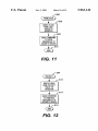
FIG. 11 is a ?oW chart of the BIOS softWare routine for
the Permanent Lock command, Which begins at step 590. In
5,963,142
13
14
step 606, the computer system S Writes the ?ash ROM lock
value to the Write protect register. The computer system S
then sends the Permanent Lock command to the security
device in step 608 before exiting in step 610.
Word to the security device, and the security device alloWs
access to the secured features. Security is enhanced in the
preferred embodiment in that the passWord cannot be
obtained from the security device: the passWord is initially
Written to it, and the security device can verify a passWord,
but the security device cannot divulge the passWord.
Additionally, the security device controls the access. If code
FIG. 12 is a ?oW chart of the BIOS softWare routine for
the Protect Resources command, Which begins at step 594.
In step 612, the computer system S Writes the ?ash ROM
protect value to Write protect register. The computer system
S then sends the Protect Resources command to the security
device in step 614 before exiting in step 616.
running on the processor could control the access, then an
attacker Would only need to ?nd out Which bits to tWiddle to
10
FIG. 13 is a ?oW chart of the BIOS softWare routine for
the Access Resources command, Which begins at step 598.
The computer system S initially checks to see if the CMOS
memory is locked in step 618. If not, the validity of the
administrator passWord is tested in step 620. If the passWord
computer system S has left secure code. Therefore an
attacker cannot utiliZe softWare to access the protected
15 device.
As shoWn in FIG. 15, after entry in step 676, the softWare
is not valid, the computer system S uses the Default Pass
Word. In this process, the computer system S then sends the
Access Resources command to the security device in step
622 and then sends the Default PassWord to the security
device in step 624.
In the event that the CMOS memory is locked in step 618,
issues an Access Resources command to the BIOS handler
at step 678. The BIOS handler then executes as described
or that the CMOS memory is not locked, but a valid
administrator passWord exists in step 620, the computer
system S sends an Access Resources command to the
security device in step 626. It then gets a byte of passWord
25
from the user in step 628 and Writes the byte to the
data/status register of the security device at step 630. Then
in step 632 the computer system S determines if the last byte
enables the security checking by the security device and the
sequence starts all over again.
The passWord is changed in the preferred embodiment by
changing the administrator passWord using existing con?gu
35
Resource request. If successful, the program Would then call
the BIOS handler With a Store PassWord request. In the Store
PassWord request the BIOS handler Would obtain the neW
not, the softWare delays one second in step 638 by Waiting
passWord, preferably con?rm it, and then Would issue the
STOREiPASSWORD command to the security device and
then provide the neW passWord to the security device. The
45
program Would then issue a Protect Resources request to the
BIOS handler.
Thus, a security device is disclosed for securing the
computer having the system ROM provide a passWord at
poWer-on to a security device Which controls access to the
secured features. Since the security device can only verify
the passWord and not divulge it, security of the system is
enhanced.
The foregoing disclosure and description of the invention
are illustrative and explanatory thereof, and various changes
register in step 644 before exiting in step 646.
Turning to FIG. 14, a ?oW chart of the BIOS softWare
routine for the Read Status command is disclosed. The
routine is entered in step 602. The softWare then sends the
Read Status command to the security device in step 650. The
ration operations. If desired, a separate program could be
provided, particularly if a passWord other than the admin
istrator passWord is utiliZed in the security device. The
program Would call the BIOS handler With an Access
indicated by the D bit being set, the softWare checks to see
if less than three passWords Were attempted in step 636. If
for the D bit to clear before restarting the sequence once
more by branching to step 626. If more than three passWords
have been attempted in step 636, failure is indicated to the
user in step 642 and the sequence is exited in step 646.
If the passWord Was correct in step 634, or if the default
passWord Was sent in step 624, the softWare branches to step
640, Where the computer system S checks on the unlocked
status of the security device. If the device is still locked, a
failure ?ag is set in step 641 to indicate failure in accessing
the security device. If the security device is unlocked in step
640 or after setting the failure ?ag in step 641, the softWare
Writes the ?ash ROM unlock value to the Write protect
above. The softWare in step 680 then checks to determine if
the failure ?ag is set or a failure to provide the proper
passWord occurred. If the access Was not successful, control
proceeds to step 682 Where the failure is indicated to the user
and then to step 690 Where the sequence ends.
If the access Was successful, the resource is unlocked and
in step 684 the desired access is made to the resource, such
as Writing a neW BIOS to the ?ash ROM 164. After the
access is completed, successfully or unsuccessfully, a Pro
tect Resources command is issued to the security device at
step 688 before exiting at step 690. This action once again
has been received. If not, control returns to step 628. Thus,
the next eight Writes to the data/status register cause each
byte Written to the data/status register to be compared
against a byte of the passWord stored in the security device.
If the last byte is encountered in step 632, the softWare then
veri?es that the passWord Was correct and accepted by
examining the D or delay bit from the security device in step
634. If the passWord is rejected by the security device as
unlock it. As the security device cannot provide the pass
Word and the CMOS memory is locked before the computer
system S is booted so that the administrator passWord also
cannot be read, the passWord is not available once the
in the siZe, shape, materials, components, circuit elements,
55
Wiring connections and contacts, as Well as in the details of
the illustrated circuitry and construction and method of
operation may be made Without departing from the spirit of
computer system S then reads the data port of the security
device to get the status in step 652 before exiting in step 654.
Turning to FIG. 15, an illustrative sequence for accessing
the invention.
We claim:
1. Asecurity device for protecting at least one resource of
a computer system, the resource having a protected state and
secured resources is shoWn. This sequence Would be
folloWed, for example, When a program Which controls
an unprotected state, access to the resource being controlled
doWnloading a neW BIOS into the ?ash ROM 164 is
by a passWord code, comprising:
executing. After a passWord has been doWnloaded to the
security device at boot-up as described above, a PROTECT
RESOURCES command can be issued to the security
device. To gain access, the user provides the correct pass
65
a memory device, comprising:
at least one memory slot for securely storing the
passWord code, the memory slot having a locked
state and an unlocked state;


![mm [mm [1 um um [11115151116 |])|]1]](http://vs1.manualzilla.com/store/data/005839409_1-1dd2adaaab9a040f039445848c9c3135-150x150.png)