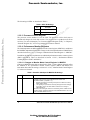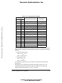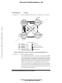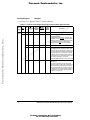
1
Freescale Semiconductor, Inc.
SA14-2056-01
(IBM Order Number)
MPC604UMAD/AD
(Motorola Order Number)
Addendum to
LE
A
SC
S
O
IC
EM
R,
O
CT
U
ND
C
IN
.
™
PowerPC 604™ RISC Microprocessor
User’s Manual:
E
E
PowerPC 604e™ Microprocessor
Supplement and
FR
Y
User’s Manual Errata
B
D
E PowerPC 604 RISC Microprocessor User’s Manual is in
This addendum toIV
the
two parts: CH
• Part
AR1: The PowerPC 604e Microprocessor Supplement provides an
0
0
overview of the 604e, with detailed information about features that differ
from those of the 604 described in the user’s manual. This information is
presented in the same order as in the user’s manual.
Note that an index is provided for Part 1 of this document.
•
Part 2: Errata to PowerPC 604 RISC Microprocessor User’s Manual
contains corrections to the user’s manual.
This document is designed to be used in conjunction with the user’s manual and
PowerPC Microprocessor Family: The Programming Environments, referred to
as The Programming Environments Manual.
In this document, the terms ‘604’, ‘604e’, ‘603’, and ‘603e’ are used as
abbreviations for ‘PowerPC 604 microprocessor’, ‘PowerPC 604e
microprocessor’, ‘PowerPC 603™ microprocessor’, and ‘PowerPC 603e™
microprocessor’, respectively. The PowerPC 604e microprocessors are available
from IBM as PPC604e and from Motorola as MPC604e.
To locate any published errata or updates for this document, refer to the website
at http://www.mot.com/powerpc/ or at http://www.chips.ibm.com/products/ppc.
The PowerPC name, PowerPC logotype, PowerPC 604e, PowerPC 604, PowerPC 603e, and PowerPC 603 are trademarks of
I.nternational Business Machines Corporation used by Motorola under license from International Business Machines Corporation.
This document contains information on a new product under development. Specifications and information herein are subject to change without notice.
© Motorola Inc. 1996
Portions hereof © International Business Machines Corp. 1991–1996. All rights reserved.
For More Information On This Product,
Go to: www.freescale.com
Addendum to 604 User’s Manual
Freescale Semiconductor, Inc...
9/96
REV 1
Freescale Semiconductor, Inc.
Part 1: The PowerPC 604e Microprocessor Supplement
Freescale Semiconductor, Inc...
This part of the document provides an overview of features of the 604e and provides
detailed information about the features that are either not implemented on or are
implemented differently from the 604.
.
NC
I
R,
1.1 Overview
O
CT
This section describes features of the 604e, provides a block diagram
showing the major
U
functional units, and describes briefly how those units interact. D
N
O
The 604e is an implementation of the PowerPC™ family
of reduced instruction set
IC
computer (RISC) microprocessors. The 604e implements
the PowerPC architecture as it is
M
specified for 32-bit addressing, which provides 32-bit
SE effective (logical) addresses, integer
E
data types of 8, 16, and 32 bits, and floating-point
data types of 32 and 64 bits (single- and
ALPowerPC implementations, the PowerPC
double-precision, respectively). For 64-bit
C
architecture provides additional 64-bit
ESinteger data types, 64-bit addressing, and related
E
features.
FR
Y
The 604e is a superscalar B
processor
capable of issuing four instructions simultaneously. As
many as seven instructions
can finish execution in parallel. The 604e has seven execution
D
units that can operate
VEin parallel:
I
• Floating-point
CH unit (FPU)
R
A processing unit (BPU)
• Branch
•
•
Condition register unit (CRU)
Load/store unit (LSU)
•
Three integer units (IUs):
— Two single-cycle integer units (SCIUs)
— One multiple-cycle integer unit (MCIU)
This parallel design, combined with the PowerPC architecture’s specification of uniform
instructions that allows for rapid execution times, yields high efficiency and throughput.
The 604e’s rename buffers, reservation stations, dynamic branch prediction, and
completion unit increase instruction throughput, guarantee in-order completion, and ensure
a precise exception model. (Note that the PowerPC architecture specification refers to all
exceptions as interrupts.)
The 604e has separate memory management units (MMUs) and separate 32-Kbyte on-chip
caches for instructions and data. The 604e implements two 128-entry, two-way set
associative translation lookaside buffers (TLBs), one for instructions and one for data, and
provides support for demand-paged virtual memory address translation and variable-sized
block translation. The TLBs and the cache use least-recently used (LRU) replacement
algorithms.
2
Addendum to PowerPC 604 RISC Microprocessor User’s Manual
For More Information On This Product,
Go to: www.freescale.com
Freescale Semiconductor, Inc.
The 604e has a 64-bit external data bus and a 32-bit address bus. The 604e interface
protocol allows multiple masters to compete for system resources through a central external
arbiter. Additionally, on-chip snooping logic maintains data cache coherency for
multiprocessor applications. The 604e supports single-beat and burst data transfers for
memory accesses and memory-mapped I/O accesses.
C.
IN
Freescale Semiconductor, Inc...
,
The 604e uses an advanced, 2.5-V CMOS process technology and is fully compatible
with
TTL devices.
OR
CT
U
1.2 PowerPC 604e Microprocessor Features
ND
O
This section summarizes features of the 604e’s implementation
of the PowerPC
IC
M
architecture.
SE
Figure 1 provides a block diagram showingLE
features of the 604e. Note that this is a
conceptual diagram that shows basic features
CA and does not attempt to show how these
features are physically implemented E
onSthe chip.
E
FR
BY
D
VE
I
CH
R
A
PowerPC 604e Microprocessor Supplement
For More Information On This Product,
Go to: www.freescale.com
3
4
16-Entry
Reorder Buffer
Store Queue
Load
Queue
32 Bit
For More Information On This Product,
Go to: www.freescale.com
DTLB
SRs
DBAT
Array
D MMU
+
64 Bit
32-Kbyte
D Cache
64 Bit
Tags
64 Bit
Tags
* +
FPSCR
/
FloatingPoint Unit
Reservation
Station (2 Entry)
128 Bit
ITLB
SRs
BUS INTERFACE
UNIT
32-Kbyte
I Cache
IBAT
Array
C
IN
64-BIT DATA BUS
64 Bit
Rename
Buffers (8)
128 Bit
I MMU
R,
O
CT
U
ND
32-BIT ADDRESS BUS
32 Bit
32 Bit
EA
Calculation
Load/Store
Unit
FPR File
S
O
IC
EM
COMPLETION
UNIT
32 Bit
32 Bit
Reservation
Station (2 Entry)
Condition
Register
Logical Unit
Reservation
Station (2 Entry)
LE
A
SC
/ +
* +
Single-Cycle
Integer Units
Rename
Buffers (12)
GPR File
Dispatch
BHT
32 Bit
EE
R
F
MultipleCycle Integer
Unit
/
*
Reservation
Station (2 Entry)
128 Bit
Reservation
Station (2)
BY
Reservation
Station (1 Entry)
CTR
LR
ED
V
I
Performance monitor
JTAG/COP
Interface
Instruction
Queue
BTAC
CR File
Rename
Buffers (8)
INSTRUCTION UNIT
Branch Processing
Unit
CH
R
A
Clock
Multiplier
Time Base
Counter/Decrementer
Fetcher
64 Bit
Freescale Semiconductor, Inc...
Freescale Semiconductor, Inc.
.
Figure 1. PowerPC 604e Microprocessor Block Diagram
Addendum to PowerPC 604 RISC Microprocessor User’s Manual
Freescale Semiconductor, Inc.
1.2.1 New Features of the PowerPC 604e Microprocessor
Features of the 604e that are not implemented in the 604 are as follows:
Freescale Semiconductor, Inc...
•
•
Additional special-purpose registers
— Hardware implementation-dependent register 1 (HID1) provides four read-only
C.
N
PLL_CFG bits for indicating the processor/bus clock ratio.
,I
R
— Three additional registers to support the performance monitor—MMCR1
is a
O
second control register that includes bits to support the useCofTtwo additional
counter registers, PMC3 and PMC4.
DU
N
Instruction execution
CO
I
— Separate execution units for branch and condition
M register (CR) instructions. The
604e implements a condition register unit
(CRU) that executes condition register
SE
logical instructions that were executed
LE in the 604’s BPU. The CRU makes it
A
possible for branch instructions
Cto execute and resolve before preceding CR
Scan
logical instructions. The 604e
dispatch one CR logical or branch instruction
E
E
per cycle, but it can execute
both
branch
and CR logical instructions at the same
FR
time.
Y
•
B in decode stage. Branch correction in the decode stage can
— Branch correction
D
now predict
branches whose target is taken from the count or link registers if no
VofEthe
I
updates
count and link register are pending. This saves at least one cycle
H
C
on
branch
correction
when the Move to Special-Purpose Register (mtspr)
AR
instruction can be sufficiently separated from the branch that uses the SPR as a
target address.
— Ability to disable the branch target address cache (BTAC)—HID0[30] has been
defined to allow the BTAC to be disabled. When HID0[30] is set, the BTAC
contents are invalidated and the BTAC behaves as if it were empty. New entries
cannot be added until the BTAC is enabled.
Enhancements to cache implementation
— 32-Kbyte, physically addressed, split data and instruction caches. Like the 604,
both caches are four-way set associative; however, each cache has twice as many
sets, logically separated into 128 sets of odd lines and 128 sets of even lines.
— Data cache line-fill buffer forwarding. In the 604, only the critical double word
of a burst operation was made available to the requesting unit at the time it was
burst into the line-fill buffer. Subsequent data was unavailable until the cache
block was filled. In the 604e, subsequent data is also made available as it arrives
in the line-fill buffer.
— Additional cache copy-back buffers. The 604e implements three copy-back write
buffers (increased from one in the 604). Having multiple copy-back buffers
provides the ability for certain instructions to take fuller advantage of the
pipelined system bus to provide more efficient handling of cache copy-back,
block invalidate operations caused by the Data Cache Block Flush (dcbf)
PowerPC 604e Microprocessor Supplement
For More Information On This Product,
Go to: www.freescale.com
5
Freescale Semiconductor, Inc.
instruction, and cache block clean operations resulting from the Data Cache
Block Store (dcbst) instruction.
Freescale Semiconductor, Inc...
•
— Coherency support for instruction fetching. Instruction fetching coherency is
controlled by HID0[23]. In the default mode, HID0[23] is 0, GBL is not asserted
.
for instruction accesses, as is the case with the 604. If the bit is set, and C
N
instruction translation is enabled (MSR[IR] = 1), the GBL signal is ,setI to reflect
the M bit for this page or block. If instruction translation is disabled
OR
T
(MSR[IR] = 0), the GBL signal is asserted for instruction fetches.
C
System interface operation
DU
N
O however, on the 604e Vdd
— The 604e has the same signal configuration as the
604;
IC must be connected to
and AVdd must be connected to 2.5 Vdc andMOVdd
3.3 Vdc. The 604e uses split voltage planes,
SE and for replacement compatibility,
E
604/604e designs should provide both
2.5-V
and 3.3-V planes and the ability to
L
A
connect those two planes together
and
disable
the 2.5-V plane for operation with
C
S
a 604.
E
E
— Support for additionalR
processor/bus
clock ratios (7:2, 5:2, and 4:1).
F
Configuration of Y
the processor/bus clock ratios is displayed through a new
B
604e-specific register,
HID1. Note that although this register is not defined by the
D
PowerPC E
architecture, it is consistent with implementation-specific registers
IV on some other processors.
implemented
H
—R
ToCsupport the changes in the clocking configuration, different precharge timings
A for the ABB, DBB, ARTRY, and SHD signals are implemented internally by the
processor. Selectable precharge timings for ARTRY and SHD can be disabled by
setting HID0[7]. Precharge timings are provided in the 604e hardware
specifications.
— No-DRTRY mode. In addition to the normal and data streaming modes
implemented on the 604, a no-DRTRY mode is implemented on the 604e that
improves performance on read operations for systems that do not use the
DRTRY signal. No-DRTRY mode makes read data available to the processor
one bus clock cycle sooner than in normal mode. In no-DRTRY mode, the
DRTRY signal is no longer sampled as part of a qualified bus grant.
— The VOLTDETGND output signal is implemented only on BGA packages as an
indicator of the core voltage.
•
•
6
Full hardware support for little-endian accesses. Little-endian accesses take
alignment exceptions for only the same set of causes as big-endian accesses.
Accesses that cross a word boundary require two accesses with the lower-addressed
word accessed first.
Additional events that can be tracked by the performance monitor.
Addendum to PowerPC 604 RISC Microprocessor User’s Manual
For More Information On This Product,
Go to: www.freescale.com
Freescale Semiconductor, Inc.
1.2.2 Overview of the PowerPC 604e Microprocessor Features
Major features of the 604e are as follows:
•
High-performance, superscalar microprocessor
— As many as four instructions can be issued per clock
C
IN
.
— As many as seven instructions can be executing per clock (including three
, integer
R
instructions)
O
Freescale Semiconductor, Inc...
T
•
— Single-clock-cycle execution for most instructions
UC
D
Seven independent execution units and two register filesN
O
— BPU featuring dynamic branch prediction
IC
M
– Two-entry reservation station
SE
E branches
– Out-of-order execution through L
two
A
C
– Shares dispatch bus with S
CRU
E
– 64-entry fully-associative
target address cache (BTAC). In the 604e,
RE branch
the BTAC can be F
disabled
and invalidated.
Y
B history table (BHT) with two bits per entry for four levels of
– 512-entry branch
D
prediction—not-taken,
strongly not-taken, taken, strongly taken
VE
I
— Condition
H register unit (CRU)
C
– Two-entry reservation station
AR
– Shares dispatch bus with BPU
— Two single-cycle IUs (SCIUs) and one multiple-cycle IU (MCIU)
– Instructions that execute in the SCIU take one cycle to execute; most
instructions that execute in the MCIU take multiple cycles to execute.
– Each SCIU has a two-entry reservation station to minimize stalls
– The MCIU has a single-entry reservation station and provides early exit (three
cycles) for 16- x 32-bit and overflow operations.
– Thirty-two GPRs for integer operands
— Three-stage floating-point unit (FPU)
– Fully IEEE 754-1985-compliant FPU for both single- and double-precision
operations
– Supports non-IEEE mode for time-critical operations
– Fully pipelined, single-pass double-precision design
– Hardware support for denormalized numbers
– Two-entry reservation station to minimize stalls
– Thirty-two 64-bit FPRs for single- or double-precision operands
PowerPC 604e Microprocessor Supplement
For More Information On This Product,
Go to: www.freescale.com
7
Freescale Semiconductor, Inc.
— Load/store unit (LSU)
– Two-entry reservation station to minimize stalls
Freescale Semiconductor, Inc...
– Single-cycle, pipelined cache access
– Dedicated adder performs EA calculations
•
•
•
C.
N
– Performs alignment and precision conversion for floating-point data
,I
R
– Performs alignment and sign extension for integer data TO
C
– Four-entry finish load queue (FLQ) provides load miss
Ubuffering
D
N
– Six-entry store queue
O
– Supports both big- and little-endian modes IC
M
Rename buffers
SE
LE
— Twelve GPR rename buffers
A
— Eight FPR rename buffers SC
E
E
— Eight condition register
(CR) rename buffers
R
F
Completion unit
BY
— Retires an instruction
from the 16-entry reorder buffer when all instructions
D
ahead IofVitEhave been completed and the instruction has finished execution.
— Guarantees
sequential programming model (precise exception model)
CH
R
A
— Monitors all dispatched instructions and retires them in order
— Tracks unresolved branches and flushes executed, dispatched, and fetched
instructions if branch is mispredicted
— Retires as many as four instructions per clock
Separate on-chip instruction and data caches (Harvard architecture)
— 32-Kbyte, four-way set-associative instruction and data caches
— LRU replacement algorithm
— 32-byte (eight-word) cache block size
— Physically indexed/physical tags. (Note that the PowerPC architecture refers to
physical address space as real address space.)
— Cache write-back or write-through operation programmable on a per page or per
block basis
— Instruction cache can provide four instructions per clock; data cache can provide
two words per clock.
— Caches can be disabled in software.
— Caches can be locked.
— Parity checking performed on both caches
8
Addendum to PowerPC 604 RISC Microprocessor User’s Manual
For More Information On This Product,
Go to: www.freescale.com
Freescale Semiconductor, Inc.
Freescale Semiconductor, Inc...
— Data cache coherency (MESI) maintained in hardware
— Secondary data cache support provided
— Instruction cache coherency optionally maintained in hardware
.
— Data cache line-fill buffer forwarding. In the 604, only the critical doubleCword
N
of the cache block was made available to the requesting unit at the time
it was
,theI cache
burst into the line-fill buffer; subsequent data was unavailable until
R
block was filled. In the 604e, subsequent data is also made available
TO as it arrives
C
in the line-fill buffer.
U
•
•
D
N
Separate memory management units (MMUs) for instructions
and data
O
C variable block size, and
— Address translation facilities for 4-Kbyte pageIsize,
M
256-Mbyte segment size
SE
— Both TLBs are 128-entry and two-way
LE set associative
A
— The page table search is performed
SC in hardware
E
— Separate IBATs and DBATs
E (four each) also defined as SPRs
R
— Separate instruction F
Y and data translation lookaside buffers (TLBs)
B
— LRU replacement algorithm
EDaddress; 32-bit physical address
— 52-bit virtual
V
HI features include the following:
Bus interface
C
AR
—
Selectable processor-to-bus clock frequency ratios (1:1, 3:2, 2:1, 5:2, 3:1, 7:2,
and 4:1)
— A 64-bit split-transaction external data bus with burst transfers
— Support for address pipelining and limited out-of-order bus transactions
— Four burst write queues—three for cache copy-back operations and one for
snoop push operations
— Two single-beat write queues
— Additional signals and signal redefinition for direct-store operations
— Provides a data streaming mode that allows consecutive burst read data transfers
to occur without intervening dead cycles. This mode also disables data retry
operations.
— No-DRTRY mode eliminates the DRTRY signal from the qualified data bus
grant condition. This improves performance on read operations for systems that
do not use the DRTRY signal. No-DRTRY mode makes read data available to
the processor one bus clock cycle sooner than if normal mode is used.
PowerPC 604e Microprocessor Supplement
For More Information On This Product,
Go to: www.freescale.com
9
Freescale Semiconductor, Inc.
Freescale Semiconductor, Inc...
•
•
•
•
Multiprocessing support features include the following:
— Hardware enforced, four-state cache coherency protocol (MESI) for data cache.
Bits are provided in the instruction cache to indicate only whether a cache block
is valid or invalid.
.
— Separate port into data cache tags for bus snooping
NC
I
— Load/store with reservation instruction pair for atomic memory references,
R,
O
semaphores, and other multiprocessor operations
CT
U
Power management
D
— Nap mode supports full shut down and snooping ON
IC
— Operating voltage of 2.5 ± 0.2 V for processor
M core, 3.3 V for external signals
E
Performance monitor can be used to help inSdebugging system designs and
improving software efficiency, especially
LEin multiprocessor systems.
A
In-system testability and debugging
SC features through JTAG boundary-scan
E
capability
E
FR
BY
1.3 PowerPC Architecture
Implementation
D
The PowerPC architecture
shares the benefits of the POWER architecture optimized for
VE
I
single-chip implementations.
The PowerPC architecture design facilitates parallel
CH and is scalable to take advantage of future technological gains.
instructionRexecution
A
This section describes the PowerPC architecture in general, and specific details about the
implementation of the 604e as a low-power, 32-bit member of the PowerPC processor
family. Note that the individual section headings indicate the chapters in the user’s manual
to which they correspond.
•
•
•
•
•
•
10
Section 1.3.1, “Features,” describes general features of the 604e with respect to the
PowerPC architecture.
Section 1.3.2, “PowerPC 604e Processor Programming Model (Chapter 2),”
describes the aspects of the register and instruction implementation that are specific
to the 604e.
Section 1.3.3, “Cache and Bus Interface Unit Operation (Chapter 3),” describes the
604e-specific cache features.
Section 1.3.4, “Exceptions (Chapter 4),” indicates that the 604e exception model is
identical to that of the 604.
Section 1.3.5, “Memory Management (Chapter 5),” indicates that the 604e MMU
implementation is identical to that of the 604.
Section 1.3.6, “Instruction Timing (Chapter 6),” describes specific characteristics of
the 604e instruction timing model.
Addendum to PowerPC 604 RISC Microprocessor User’s Manual
For More Information On This Product,
Go to: www.freescale.com
Freescale Semiconductor, Inc.
•
Section 1.3.7, “Signal Descriptions (Chapter 7),” describes differences in the
operation of the signals implemented on the 604e.
•
Section 1.3.8, “System Interface Operation (Chapter 8),” describes differences in the
604e bus protocol.
.
Freescale Semiconductor, Inc...
•
NC
Section 1.3.9, “Performance Monitor (Chapter 9),” defines additional features
, I and
R
changes in the 604e implementation of the performance monitor. O
CT
U
ND
1.3.1 Features
The 604e is a high-performance, superscalar implementationOof the PowerPC architecture.
IC architecture specifications but
Like other PowerPC processors, it adheres to the PowerPC
M
also has additional features not defined by the architecture.
These features do not affect
SE
software compatibility. The PowerPC architecture
allows optimizing compilers to schedule
E
instructions to maximize performance through
AL efficient use of the PowerPC instruction set
C
and register model. The multiple, independent
execution units in the 604e allow compilers
ES throughput.
E
to maximize parallelism and instruction
Compilers that take advantage of the
FR can additionally optimize instruction processing of
flexibility of the PowerPC architecture
the PowerPC processors. BY
D
E summarize the features of the 604e, including both those that are
The following sections
IV
defined by the H
architecture
and those that are unique to the 604e implementation.
C
The PowerPC
AR architecture consists of the following layers, and adherence to the PowerPC
architecture can be measured in terms of which of the following levels of the architecture
is implemented:
•
PowerPC user instruction set architecture (UISA)—Defines the base user-level
instruction set, user-level registers, data types, floating-point exception model,
memory models for a uniprocessor environment, and programming model for a
uniprocessor environment.
•
PowerPC virtual environment architecture (VEA)—Describes the memory model
for a multiprocessor environment, defines cache control instructions, and describes
other aspects of virtual environments. Implementations that conform to the VEA
also adhere to the UISA, but may not necessarily adhere to the OEA.
•
PowerPC operating environment architecture (OEA)—Defines the memory
management model, supervisor-level registers, synchronization requirements, and
the exception model. Implementations that conform to the OEA also adhere to the
UISA and the VEA.
For more information, refer to The Programming Environments Manual.
PowerPC 604e Microprocessor Supplement
For More Information On This Product,
Go to: www.freescale.com
11
Freescale Semiconductor, Inc.
Freescale Semiconductor, Inc...
The 604e complies to all three levels of the PowerPC architecture. Note that the PowerPC
architecture defines additional instructions for 64-bit data types. These instructions cause
an illegal instruction exception on the 604e. PowerPC processors are allowed to have
implementation-specific features that fall outside, but do not conflict with, the PowerPC
architecture specification. Examples of features that are specific to the 604e include
C. the
N
performance monitor and nap mode.
,I
OR
T
1.3.2 PowerPC 604e Processor Programming ModelC(Chapter 2)
The 604e and 604 implement the register set required by the 32-bit
portion of the PowerPC
DU
N
architecture. In addition, the 604e supports all 604-specific
registers
as well as several
O
IC
604e-specific registers, as described in this section.
M
Figure 2 shows the registers implemented in the 604e,
SE indicating those that are defined by
the PowerPC architecture and those that are 604e-specific.
All registers except the FPRs are
LE
A
32 bits wide.
C
ES
E
FR
BY
D
VE
I
CH
R
A
12
Addendum to PowerPC 604 RISC Microprocessor User’s Manual
For More Information On This Product,
Go to: www.freescale.com
Freescale Semiconductor, Inc.
SUPERVISOR MODEL—OEA
Configuration Registers
USER MODEL
UISA
General-Purpose
Registers
Freescale Semiconductor, Inc...
GPR1
GPR31
Floating-Point
Registers
FPR0
FPR1
MSR
ED
V
I
C
IN
.
R,
O
HID1
SPR 1009
CT PVR SPR 287
U
Memory Management Registers
ND
O
Instruction BAT
Data BAT Registers
Registers
Segment Registers
ICSPR 536
DBAT0U
M
SR0
IBAT0U
SPR 528
E SPR 537
SDBAT0L
SR1
SPR 529
IBAT0L
E DBAT1U SPR 538
IBAT1U
SPR 530 L
SPR 539
DBAT1L
A
SPRC
531
IBAT1L
DBAT2U SPR 540
SR15
S
SPR 532
IBAT2U E
DBAT2L
SPR 541
E
SDR1
IBAT2L
SPR 533
DBAT3U SPR 542
FR SPR
534
IBAT3U
SDR1
SPR 25
SPR 543
DBAT3L
BY IBAT3L SPR 535
Condition Register
CH
R
Floating-Point
Status
A
CR
Machine State
Register
HID0
SPR 1008
Hardware Implementation
Dependent Register 11
GPR0
FPR31
Hardware Implementation
Dependent Register 01
and Control Register
FPSCR
Performance
Monitor Counters1
Processor Version
Register
Performance Monitor
Monitor Control1
Sampled Data/
Instruction Address1
PMC1
SPR 953
MMCR0
SPR 952
SDA
SPR959
PMC2
SPR 954
MMCR1
SPR 956
SIA
SPR 955
PMC3
SPR 957
PMC4
SPR 958
Exception Handling Registers
XER
XER
SPRGs
SPR 1
Link Register
LR
SPR 8
Count Register
CTR
SPR 272
SPRG1
SPR 273
SPRG2
SPR 274
SPRG3
SPR 275
Time Base Facility
(For Reading)
TBL
TBR 268
TBU
TBR 269
1604e-specific—not
Save and Restore
Registers
SRR0
SPR 26
SRR1
SPR 27
DSISR
DSISR
SPR 18
Data Address
Register
DAR
SPR 19
Miscellaneous Registers
SPR 9
USER MODEL
VEA
2 Optional
SPRG0
Time Base Facility
(For Writing)
TBL
SPR 284
TBU
SPR 285
External Access
Register 2
EAR
Instruction Address
Breakpoint Register1
IABR
SPR 1010
Data Address
Breakpoint Register2
DABR
Processor
Identification Register2
PIR
SPR 1023
Decrementer
SPR 1013
DEC
SPR 22
SPR 282
defined by the PowerPC architecture
to the PowerPC Architecture
Figure 2. Programming Model—PowerPC 604e Microprocessor Registers
PowerPC 604e Microprocessor Supplement
For More Information On This Product,
Go to: www.freescale.com
13
Freescale Semiconductor, Inc.
The 604e includes the following registers not defined by the PowerPC architecture that are
either not provided in the 604 or incorporate changes from the 604 implementation:
•
Freescale Semiconductor, Inc...
•
•
•
•
Hardware implementation-dependent register 1 (HID1)—This register, which is not
implemented in the 604, is used to display the PLL configuration. This register. is
described in Section 1.3.2.2, “HID1—PLL Configuration Register.”
NC
I
, used to
Performance monitor counter registers (PMC3–PMC4). The countersRare
O
record the number of times a certain event has occurred. PMC3 and
PMC4
are not
T
implemented in the 604. PMC1 and PMC2 are implementedUinCthe 604 and are
described in the user’s manual. See Section 1.3.2.4.3, “Performance
Monitor
ND
Counter Registers (PMC3 and PMC4),” for more information.
O
IC
Performance monitor mode control register 0 (MMCR0)—MMCR0
has additional
M
E
bits not described in the user’s manual. TheSadditional
bits are described in Section
E Register 0—MMCR0.”
1.3.2.4.1, “Changes to Monitor Mode L
Control
A
Cregister 1 (MMCR1)—The performance
Performance monitor mode control
ES for enabling various performance monitoring
monitor control registers areEused
R
interrupt conditions andFestablishes
the function of the counters. MMCR1 is not
implemented in the 604.
See
Section
1.3.2.4.2, “Monitor Mode Control Register 1—
BY
MMCR1,” for more
information.
D
Hardware Iimplementation-dependent
register 0 (HID0)—This register is used to
VE
control H
various functions within the 604 and 604e, such as enabling checkstop
RC and locking, enabling, and invalidating the instruction and data caches.
conditions,
A
Additional bits defined in the HID0 register disable the BTAC, control whether
coherency is maintained for instruction fetches, and disable the default precharge
values for the shared (SHD) and address retry (ARTRY) signals. The 604e defines
additional bits not included in the 604 implementations of the HID0 register. These
bits are described in Section 1.3.2.1, “PowerPC 604e-Specific Bits in HID0.”
Note that while it is not guaranteed that the implementation of HID registers is consistent
among PowerPC processors, other processors may be implemented with similar or
identical HID registers.
1.3.2.1 PowerPC 604e-Specific Bits in HID0
The 604e has three additional bits in HID0, described in Table 1. The HID0 bits not shown
here are implemented as they are in the 604 and are described in Section 2.1.2.3, “Hardware
Implementation-Dependent Register 0,” in the user’s manual.
14
Addendum to PowerPC 604 RISC Microprocessor User’s Manual
For More Information On This Product,
Go to: www.freescale.com
Freescale Semiconductor, Inc.
Table 1. Additional HID0 Bits
Freescale Semiconductor, Inc...
Bit
Description
C
IN
.
12
Reserved. This bit should always be set to zero.
23
Coherent instruction fetch enable—controls whether instruction fetch bus operations are snooped.
0
In this default state, all instruction fetch address tenures are nonglobal, regardless of the state of the
MSR[IR] or the WIMG bits. Therefore, coherency checking on instruction fetches is disabled, as it is on
the 604.
1
The 604e presents a value on the GBL signal for instruction fetch address tenures that reflects the state
of the M bit if MSR[IR] = 1. If IR = 0 and HID0[23] is set, the GBL signal is asserted for all instruction
fetch address tenures.
When modifying the instruction cache enable or instruction cache lock bits, software should place an isync
instruction after the mtspr[HID0] instruction to ensure that the subsequent instructions are fetched with the
proper cache mode.
Note that, like the 604, the 604e never snoops its data cache during its own instruction fetch address tenure,
regardless of the state of GBL. Therefore, assertion of the GBL signal does not guarantee coherency
between the 604e’s own instruction cache and data cache. As in the 604, coherency between the instruction
and data caches must be maintained by software.
Additional information is provided in Section 1.3.3.1, “Instruction Cache.”
30
BY
EE
R
F
LE
A
SC
S
O
IC
EM
R,
O
CT
U
ND
BTAC disable—used to disable use of the 64-entry branch target address cache.
0
The BTAC is enabled and new entries can be added.
1
The BTAC contents are invalidated and the BTAC behaves as if it were empty. New entries cannot be
added until the BTAC is enabled.
Note that the BTAC can be flushed by disabling and re-enabling the BTAC using two successive mtspr
instructions.
CH
R
A
ED
V
I
When modifying the data cache enable or data cache lock bits, software should place a sync
instruction both before and after the move to the HID0 register to ensure that the data cache
is properly updated by instructions both before and after the move to HID0 instruction.
1.3.2.2 HID1—PLL Configuration Register
The 604e has added HID1, (SPR 1009), shown in Figure 3. HID1 is a supervisor-level
register that allows software to read the current PLL_CFG value. The PLL_CFG signal
values are read from bits HID1[0–3]. The remaining bits are reserved and are read as zeros.
HID1 is a read-only register.
Reserved
0000
0
0000
0000
0000
0000
0000
3 4
0000
31
Figure 3. HID1 Clock Configuration Register
PowerPC 604e Microprocessor Supplement
For More Information On This Product,
Go to: www.freescale.com
15
Freescale Semiconductor, Inc.
The bit settings in HID1 are described in Table 2.
Table 2. HID1 Bit Settings
Bits
Description
0–3
PLL configuration bits (0–3)
4–31
Reserved (Read as zero)
Freescale Semiconductor, Inc...
1.3.2.3 Processor Version Register
R,
O
CT
U
ND
C
IN
.
The processor version number is 9 for the 604e. The processor revision level starts at
O
0x0100 and changes for each chip revision. The revision
IClevel is updated on all silicon
revisions. For more information, see “Processor Version
EM Register (PVR),” in Chapter 2,
S
“PowerPC Register Set,” of The Programming Environments Manual.
LE
A
1.3.2.4 Performance Monitor Registers
SC
E
The 604e implements an additionalEmonitor mode control register (MMCR1) in addition to
the MMCR0 implemented in the
FR604. Changes to the 604e implementation of MMCR0 are
described in Section 1.3.2.4.1,
BY “Changes to Monitor Mode Control Register 0—MMCR0.”
D
In addition, the 604eE
implements two additional performance monitor counter registers
V also
I
(PMC3 and PMC4).
These
are described in Section 1.3.2.4.3, “Performance Monitor
H
C
Counter Registers
(PMC3
and
PMC4).”
AR
1.3.2.4.1 Changes to Monitor Mode Control Register 0—MMCR0
Changes to MMCR0 in the 604e are described in Table 3. These changes primarily reflect
the addition of two performance monitor counter registers (PMC3 and PMC4). For
information about other bit settings, see Section 2.1.2.4.1, “Monitor Mode Control Register
0,” in the user’s manual.
Table 3. PowerPC 604e-Specific MMCR0 Bit Settings
Bits
Name
6
DISCOUNT
16
Description
Disable counting of PMC1–PMC4 when a performance monitor interrupt is
signalled or the occurrence of an enabled time base transition with
((INTONBITTRANS =1) & (ENINT = 1)).
0
Signalling a performance monitoring interrupt does not affect the counting
status of PMC1–PMC4.
1
The signalling of a performance monitoring interrupt prevents the changing
of the PMC1 counter. The PMC2–PMC4 counters does not change if
PMCTRIGGER = 0.
Because, a time base signal could have occurred along with an enabled counter
negative condition, software should always reset INTONBITTRANS to zero, if the
value in INTONBITTRANS was a one.
Addendum to PowerPC 604 RISC Microprocessor User’s Manual
For More Information On This Product,
Go to: www.freescale.com
Freescale Semiconductor, Inc.
Freescale Semiconductor, Inc...
Table 3. PowerPC 604e-Specific MMCR0 Bit Settings (Continued)
Bits
Name
Description
10–15
THRESHOLD
Threshold value. All 6 bits are supported by the 604e. The threshold value is
multiplied by 4, allowing threshold values from 0 to 252 in increments of 4. The
intent of the THRESHOLD support is to be able to characterize L1 data cache
misses.
17
PMCINTCONTROL
Enable interrupt signalling due to any PMCn (n>1) counter negative.
0
Disable PMCn (n>1) interrupt signalling due to PMCn (n>1) counter
negative.
1
Enable PMCn (n>1) interrupt signalling due to PMCn (n>1) counter
negative.
18
PMCTRIGGER
PMCTRIGGER may be used to trigger counting of PMCn (n>1) after PMC1 has
become negative or after a performance monitoring interrupt is signalled.
0
Enable PMCn (n>1) counting
1
Disable PMCn (n>1) counting until PMC1 bit 0 is “on” or until a performance
monitor interrupt is signalled.
PMCTRIGGER may be used to trigger counting of PMCn (n>1) after PMC1 has
become negative. This provides a triggering mechanism to allow counting after a
certain condition occurs or after enough time has occurred. It can be used to
support getting the count associated with a specific event.
BY
EE
R
F
LE
A
SC
S
O
IC
EM
R,
O
CT
U
ND
C
IN
.
1.3.2.4.2 Monitor Mode
Control Register 1—MMCR1
ED
V
The 604e definesIan additional monitor mode control register (MMCR1), which functions
H
as an event Cselector
for the two 604e-specific performance monitor counter registers
R
(PMC3 and
A PMC4). MMCR1 is SPR 956. The MMCR1 register is shown in Figure 4.
Reserved
0000000000000000000000000000
PMC3SELECT PMC4SELECT
0
4 5
9 10
31
Figure 4. Monitor Mode Control Register 1 (MMCR1)
Bit settings for MMCR1 are shown in Table 4. The corresponding events are described in
the Section 1.3.2.4.3, “Performance Monitor Counter Registers (PMC3 and PMC4).”
Table 4. MMCR1 Bit Settings
Bits
Name
Description
0–4
PMC3SELECT
PMC3 event selector
5–9
PMC4SELECT
PMC4 event selector
10–31
—
Reserved
PowerPC 604e Microprocessor Supplement
For More Information On This Product,
Go to: www.freescale.com
17
Freescale Semiconductor, Inc.
1.3.2.4.3 Performance Monitor Counter Registers (PMC3 and PMC4)
The 604e implements two additional performance monitor counter registers, PMC3 and
PMC4. PMC3 is SPR 957 and PMC4 is SPR 958. The events are described in Table 5 and
Table 6.
R,
O
CT
U
ND
Table 5. Selectable Events—PMC3
Freescale Semiconductor, Inc...
MMCR1[0–4]
Comments
0 0000
Register counter holds current value.
0 0001
Count every cycle.
0 0010
Indicates the number of instructions being completed every cycle
0 0011
0 0100
0 0101
0 0110
0 0111
0 1000
O
IC
EM
C
IN
.
S
E
L
CtoABIU or cache busy. Counts cycles between when a load or
Number of cycles the LSU stalls due
S
store request is made and a response
was expected. For example, when a store is retried, there
EE instruction is presented to the cache again. Cycles in between are
are four cycles before the same
R
not counted.
F
Number of cycles
BYthe LSU stalls due to a full store queue
D
NumberE
of cycles the LSU stalls due to operands not available in the reservation station
V
Number
HI of instructions written into the load queue. Misaligned loads are split into two transactions
C
with the first part always written into the load queue. If both parts are cache hits, data is returned to
AR the rename registers and the first part is flushed from the load queue. To count the instructions that
RTCSELECT bit transition. 0 = 47, 1 = 51, 2 = 55, 3 = 63 (bits from the time base lower register).
Number of instructions dispatched
enter the load queue to stay, the misaligned load hits must be subtracted. See event 8 in Table 6.
0 1001
Number of cycles that completion stalls for a store instruction
0 1010
Number of cycles that completion stalls for an unfinished instruction. This event is a superset of
PMC3 event 9 and PMC4 event 10.
0 1011
Number of system calls
0 1100
Number of cycles the BPU stalled as branch waits for its operand
0 1101
Number of fetch corrections made at the dispatch stage. Prioritized behind the execute stage.
0 1110
Number of cycles the dispatch stalls waiting for instructions
0 1111
Number of cycles the dispatch stalls due to unavailability of reorder buffer (ROB) entry. No ROB
entry was available for the first nondispatched instruction.
1 0000
Number of cycles the dispatch unit stalls due to no FPR rename buffer available. First
nondispatched instruction required a floating-point reorder buffer and none was available.
1 0001
Number of instruction table search operations
1 0010
Number of data table search operations. Completion could result from a page fault or a PTE
match.
1 0011
Number of cycles the FPU stalled
1 0100
Number of cycles the SCIU1 stalled
1 0101
Number of times the BIU forwards noncritical data from the line-fill buffer
18
Addendum to PowerPC 604 RISC Microprocessor User’s Manual
For More Information On This Product,
Go to: www.freescale.com
Freescale Semiconductor, Inc.
Table 5. Selectable Events—PMC3 (Continued)
MMCR1[0–4]
C.
N
1 0111
Number of data bus transactions completed with two data bus transactions queued behind
,I
R
1 1000
Counts pairs of back-to-back burst reads streamed without a dead cycle between
O them in data
T
streaming mode
UC
1 1001
Counts non-ARTRYd processor kill transactions caused by a write-hit-on-shared
condition
D
N
1 1010
This event counts non-ARTRYd write-with-kill address operations
O that originate from the three
castout buffers. These include high-priority write-with-killIC
transactions caused by a snoop hit on
modified data in one of the BIU’s three copy-back buffers.
When the cache block on a data cache
EM buffers.
miss is modified, it is queued in one of three copy-back
The miss is serviced before the
S
copy-back buffer is written back to memoryE
as a write-with-kill transaction.
AL buffers are occupied
1 1011
Number of cycles when exactly two castout
C
ESretried due to occupied castout buffers
1 1100
Number of data cache accesses
E
1 1101
Number of read transactions
FR from load misses brought into the cache in a shared state
Y
1 1110
CRU IndicatesB
that a CR logical instruction is being finished.
D
VE events for PMC4.
Table 6 lists the selectable
I
CH
Table 6. Selectable Events—PMC4
R
A
1 0110
Freescale Semiconductor, Inc...
Comments
Number of data bus transactions completed with pipelining one deep with no additional bus
transactions queued behind it
MMCR1[5–9]
Description
0 0000
Register counter holds current value
0 0001
Count every cycle
0 0010
Number of instructions being completed
0 0011
RTCSELECT bit transition. 0 = 47, 1 = 51, 2 = 55, 3 = 63 (bits from the time base lower register).
0 0100
Number of instructions dispatched
0 0101
Number of cycles the LSU stalls due to busy MMU
0 0110
Number of cycles the LSU stalls due to the load queue full
0 0111
Number of cycles the LSU stalls due to address collision
0 1000
Number of misaligned loads that are cache hits for both the first and second accesses. Related to
event 8 in PMC3.
0 1001
Number of instructions written into the store queue
0 1010
Number of cycles that completion stalls for a load instruction
0 1011
Number of hits in the BTAC. Warning—if decode buffers cannot accept new instructions, the
processor refetches the same address multiple times.
0 1100
Number of times the four basic blocks in the completion buffer from which instructions can be
retired were used
PowerPC 604e Microprocessor Supplement
For More Information On This Product,
Go to: www.freescale.com
19
Freescale Semiconductor, Inc.
Table 6. Selectable Events—PMC4 (Continued)
MMCR1[5–9]
.
0 1101
Number of fetch corrections made at decode stage
0 1110
Number of cycles the dispatch unit stalls due to no unit available. First nondispatched instruction
requires an execution unit that is either full or a previous instruction is being dispatched to that unit.
0 1111
Freescale Semiconductor, Inc...
Description
1 0000
1 0001
1 0010
1 0011
1 0100
1 0101
1 0110
1 0111
1 1000
1 1001
C
IN
R,
O
CT
U
Number of cycles the dispatch unit stalls due to no CR rename buffer
D available. First
nondispatched instruction requires a CR rename buffer and none
is available.
N
O
Number of cycles the dispatch unit stalls due to CTR/LRIC
interlock. First nondispatched instruction
could not dispatch due to CTR/LR/mtcrf interlock. M
SE
Number of cycles spent doing instruction table search operations
E
ALsearch operations
Number of cycles spent doing data table
C
S
Number of cycles SCIU0 wasE
stalled
E
Number of cycles MCIUR
F was stalled
Number of bus cycles
BY after an internal bus request without a qualified bus grant
D
NumberE
of data bus transactions completed with one data bus transaction queued behind
V
I
Number
H of write data transactions that have been reordered before a previous read data
transaction using the DBWO feature
C
AR Number of ARTRYd processor address bus transactions
Number of cycles the dispatch unit stalls due to unavailability of GPR rename buffer. First
nondispatched instruction requires a GPR reorder buffer and none are available.
1 1010
Number of high-priority snoop pushes. Snoop transactions, except for write-with-kill, that hit
modified data in the data cache cause a high-priority write (snoop push) of that modified cache
block to memory.This operation has a transaction type of write-with-kill. This event counts the
number of non-ARTRYd processor write-with-kill transactions that were caused by a snoop hit on
modified data in the data cache. It does not count high-priority write-with-kill transactions caused
by snoop hits on modified data in one of the BIU’s three copy-back buffers.
1 1011
Number of cycles for which exactly one castout buffer is occupied
1 1100
Number of cycles for which exactly three castout buffers are occupied
1 1101
Number of read transactions from load misses brought into the cache in an exclusive (E) state
1 1110
Number of undispatched instructions beyond branch
1.3.2.5 Support for Misaligned Little-Endian Accesses
The 604e provides hardware support for misaligned little-endian accesses. Little-endian
accesses in the 604e take an alignment exception for the same cases that big-endian
accesses take alignment exceptions. Any data access that crosses a word boundary requires
two accesses regardless of whether the data is in big- or little-endian format. When two
accesses are required, the lower addressed word (in the current addressing mode) is
accessed first. Consider the memory mapping in Figure 5.
20
Addendum to PowerPC 604 RISC Microprocessor User’s Manual
For More Information On This Product,
Go to: www.freescale.com
Freescale Semiconductor, Inc.
Freescale Semiconductor, Inc...
Big-Endian Mode
Contents
A
B
C
D
E
F
G
H
Address
00
01
02
03
04
05
06
07
Contents
I
J
K
L
Address
08
09
0A
0B
Little-Endian Mode
Contents
A
B
C
D
P ,
R
O
0C
0D
0E T 0F
C
U
D
N
O
IC F
E
G
H
M
E
M
N
O
C
IN
.
02
01
00
S 03
E
AL
Contents
I
J
K
L
M
N
O
P
C
S
Address
0F
0E
0D
0C
0B
0A
09
08
EE
R
F
Figure 5. Big-Endian
and Little-Endian Memory Mapping
BY
If two bytes are requested
ED starting at little-endian address 0x3, one byte at big-endian
V
address 0x4 containing
data E is accessed first followed by one byte at big-endian address
I
Hdata
0x3 containing
D. For a load halfword, the data written back to the GPR would be
C
R bytes are requested starting at little-endian address 0x6, two bytes at
D, E. IfAfour
Address
07
06
05
04
big-endian address 0x0 containing data A, B are accessed first followed by two bytes at
big-endian address 0xE containing data O, P. For a load word, the data written back to the
GPR would be O, P, A, B.
Misaligned little-endian accesses to direct-storage segments are boundedly-undefined.
1.3.2.6 Instruction Set
The 604e implements the same set of instructions that are implemented in the 604; that is,
the entire PowerPC instruction set (for 32-bit implementations) and most optional
PowerPC instructions. For information, see Section 2.3.3, “Instruction Set Overview,” in
the user’s manual. The following changes affect information provided in the user’s manual.
•
•
The undefined result of an integer divide overflow differs from that of the 604.
Changes to the behavior of the dcbst and dcbtst instructions are described in
Section 1.3.3.4, “Changes to dcbt/dcbtst Instruction Behavior.”
PowerPC 604e Microprocessor Supplement
For More Information On This Product,
Go to: www.freescale.com
21
Freescale Semiconductor, Inc.
Freescale Semiconductor, Inc...
1.3.3 Cache and Bus Interface Unit Operation (Chapter 3)
The 604e has separate 32-Kbyte data and instruction caches. This is double the size of the
604 caches. The 604e caches are logically organized as a four-way set with 256 sets
compared to the 604’s 128 sets. The physical address bits that determine the set are
19
C. of
through 26 with 19 being the most-significant bit of the index. If bit 19 is zero, theNblock
I and the
data is an even 4-Kbyte page that resides in sets 0–127; otherwise, bit 19 is,one
R
block of data is an odd 4-Kbyte page that resides in sets 128–255. Because
O the caches are
T
four-way set-associative, the cache set element (CSE0–CSE1) signals
remain
unchanged
C
U
from the 604. Figure 6 shows the organization of the caches.
D
Sets128–255
(odd pages)
Sets 0–127
(even pages)
Block 0 Address Tag 0
Block 1 Address Tag
E1D
V
HITag 2
Block 2 Address
C
Address Tag 3
Block 3
AR
BY
EE
R
F
LE
A
SC
S
N
O
IC
M
E
State
Words 0–7
State
Words 0–7
State
Words 0–7
State
Words 0–7
8 Words/Block
Figure 6. Cache Unit Organization
1.3.3.1 Instruction Cache
The 604e’s 32-Kbyte, four-way set-associative instruction cache is physically indexed.
Within a single cycle, the instruction cache provides up to four instructions.
The 604e provides coherency checking for instruction fetches. Instruction fetching
coherency is controlled by HID0[23]. In the default mode, HID0[23] is 0 and the GBL
signal is not asserted for instruction accesses on the bus, as is the case with the 604. If the
bit is set and instruction translation is enabled (MSR[IR] = 1), the GBL signal is set to
reflect the M bit for this page or block. If HID0[23] is set and instruction translation is
disabled (MSR[IR] = 0), the GBL signal is asserted and coherency is maintained in the
instruction cache.
The PowerPC architecture defines a special set of instructions for managing the instruction
cache. The instruction cache can be invalidated entirely or on a cache-block basis. In
addition, the instruction cache can be disabled and invalidated by setting the HID0[16] and
HID0[20] bits, respectively. The instruction cache can be locked by setting HID0[18].
22
Addendum to PowerPC 604 RISC Microprocessor User’s Manual
For More Information On This Product,
Go to: www.freescale.com
Freescale Semiconductor, Inc.
1.3.3.2 Data Cache
The 604e’s data cache is a 32-Kbyte, four-way set-associative cache. It is a
physically-indexed, nonblocking, write-back cache with hardware support for reloading on
cache misses. Within one cycle, the data cache provides double-word access to the LSU.
.
Freescale Semiconductor, Inc...
C
The 604e provides additional support for data cache line-fill buffer forwarding. IInNthe 604,
,
only the critical double word of a burst operation was made available to the R
requesting
unit
O
at the time it was burst into the line-fill buffer. Subsequent data was unavailable
until
the
CT as it arrives in
cache block was filled. On the 604e, subsequent data is also made U
available
the line-fill buffer.
ND
O
The 604e implements three copy-back write buffers (the
IC 604 has one). The additional
M
copy-back buffers allow certain instructions to take
further
advantage of the pipelined
E
system bus to provide highly efficient handlingSof cache copy-back operations, block
LEBlock Flush (dcbf) instruction, and cache
invalidate operations caused by the Data Cache
A
block clean operations resulting from theCData Cache Block Store (dcbst) instruction.
ES
Like the 604, the data cache tags are
RE dual-ported, so snooping does not affect the internal
operation of other transactionsFon the system interface. If a snoop hit occurs in a modified
Y
block, the LSU is blockedBinternally
for one cycle to allow the eight-word block of data to
D
be copied to the write-back
buffer,
if
necessary.
E
V
Like the instruction
HI cache, the data cache can be invalidated all at once or on a per cache
C
block basis.
The data cache can be disabled and invalidated by setting the HID0[17] and
AR
HID0[21]
bits, respectively. The data cache can be locked by setting HID0[19].
1.3.3.3 Data Cache Line-Fill Buffer Forwarding
When a load misses the cache, it is placed into the load queue. The critical data comes back
first and is unconditionally forwarded to the load/store unit. If a subsequent in-order load
to the same cache block hits on valid data in the data line-fill buffer, it is forwarded to the
load/store unit from the line-fill buffer. In the 604, a subsequent in-order load to the same
cache block is required to wait until the line-fill buffer is completely written into the cache
before data is accessed from the cache.
1.3.3.4 Changes to dcbt/dcbtst Instruction Behavior
Both the 604 and the 604e treat the dcbt and dcbtst instructions as no-ops if any of the
following conditions is met:
•
•
•
The address misses in the TLB and in the BAT.
The address is directed to a direct-store segment.
The address is directed to a cache-inhibited page.
The 604e also treats the instructions as no-ops if the data cache lock bit HID0[19] is set.
PowerPC 604e Microprocessor Supplement
For More Information On This Product,
Go to: www.freescale.com
23
Freescale Semiconductor, Inc.
1.3.3.5 Snooping Protocol Change for Read-with-Intent-to-Modify
Bus Operations
Freescale Semiconductor, Inc...
It is now illegal for any snooping device to generate a SHD snoop response without an
ARTRY response to a RWITM address tenure. This change is required for the 604. and
604e. This change is also effective for later revisions of the 604. For more information,
NC see
the entry for “Section 3.9.6, Page 3-21” in Part 2: “Errata to PowerPC, I604 RISC
Microprocessor User’s Manual,” of this document.
OR
CT
U
1.3.3.6 Two Additional Cache Copy-Back Write Buffers
D
N
The 604e bus interface unit has six write buffers, four for burst
write operations and two for
O
single-beat operations.
IC
M
E cache block of data for burst
• The four burst write buffers can hold a full S
32-byte
E buffers, one is a snoop push buffer and
write data bus tenures. Of the four burstLwrite
the other three are cache copy-back
buffers.
CA
S
— The snoop push buffer is dedicated
for snoop push write operations.
EE
R
— The three copy-backFbuffers are used for cache copy-back operations, block
invalidates dueB
toY
the Data Cache Block Flush (dcbf) instruction or block cleans
due to the Data
Cache Block Store (dcbst) instruction.
D
E
Vtwo
• Each of the
single-beat write buffers can hold up to 8 bytes of data.
I
H
C
The 604 implements
only one copy-back buffer, but is otherwise the same as the 604e
AR
implementation.
Typically, these three copy-back buffers are written to memory in the same order in which
they are filled, having the lowest priority access among all the bus interface unit’s memory
queues. Write operations from these buffers can occur out-of-order under the two following
conditions:
•
A snoop hit on one or more copy-back buffers causes the copy-back buffers to have
the second highest priority among the BIU’s memory queues, after only the
snoop-push buffer. In this case, the next write from these three copy-back buffers
will be from the buffer that contains the newest data corresponding to the snoop hit.
If the snoop address hit on multiple copy-back buffers (possibly due to the dcbst
instruction), the accesses for all matching buffers except the one with the newest
data are cancelled.
•
Similarly, if execution of the dcbst instruction causes multiple copy-back buffers to
contain the same address, each buffer that contains this address is cancelled unless
it contains the newest data or unless the buffer is the next address transaction to go
to the bus.
The three copy-back buffers in the 604e notably improve the performance of multiple dcbf
and dcbst instructions because the address and data tenures of burst writes can be pipelined.
24
Addendum to PowerPC 604 RISC Microprocessor User’s Manual
For More Information On This Product,
Go to: www.freescale.com
Freescale Semiconductor, Inc.
1.3.4 Exceptions (Chapter 4)
The 604e implements the same set of exceptions as the 604, as described in the user’s
manual.
C
IN
1.3.5 Memory Management (Chapter 5)
R,
O
CT
1.3.6 Instruction Timing (Chapter 6)
U
D
The 604e instruction timing model has a few changes from theN
604, although it is basically
O
the same design. A conceptual model of the 604eIC
hardware design showing the
relationships between the various units that affectEM
the instruction timing is shown in
S
Figure 7.
E
L
CA
branch
S
Dispatch
Unit
correction
E (Four-instruction
Fetch Unit
E
dispatch)
FR
Y
instruction dispatch
B buses
D
E operand buses
VGPR
I
GPR result buses
CH
R
FPR operand buses
A
The 604e MMU implementation is the same as is used in the 604.
FPR result
CR result bus
RS(1)
RS(2)
CRU
BPU
SCIU
MCIU
LSU
SCIU
RS(2)
FPU
32 FPRs
RS(2)
FPR
Rename
Buffers
RS(2) RS(2)
32 GPRs
RS(2)
GPR
Rename
Buffers
Freescale Semiconductor, Inc...
.
result status buses
Completion
Unit
32-Kbyte data cache
4-way, 8 words/block
Result buses
Operand buses
Figure 7. Block Diagram—Internal Data Paths
PowerPC 604e Microprocessor Supplement
For More Information On This Product,
Go to: www.freescale.com
25
Freescale Semiconductor, Inc.
The instruction timing in the 604e incorporates the following changes:
Freescale Semiconductor, Inc...
•
•
•
Addition of a condition register unit (CRU)—The CRU executes all condition
register logical and flow control instructions. Because the CRU shares the dispatch
bus with the BPU, only one condition register or branch instruction can be issued. per
clock cycle. In the 604, the CR logical unit operations are handled by the BPU.
NC The
I
addition of the CRU allows branch instructions to potentially execute/resolve
, before
R
a preceding CR logical instruction. Although one CR logical or branch
instruction
TO
can be dispatched per clock cycle, both branch and CR logicalCinstructions
can
U
execute simultaneously. Branches are still executed in order
with
respect
to
other
D
N
branch instructions. If either the CR logical reservation
station
or
the
branch
CO
reservation station is full then no instructions can Ibe
dispatched to either unit.
M
Branch correction in decode stage—Branch correction
in the decode stage has been
SE
modified to predict branches whose target
is taken from the CTR or LR. This
E
correction occurs if no CTR or LR updates
AL are pending. This correction like all other
C
decode stage corrections is doneSonly on the first two instructions of the decode
stage. This correction saves E
atE
least one cycle on branch correction when the mtspr
R
instruction can be separated
from
the branch that uses the SPR as a target address.
F
Y
Instruction fetch when
B translation is disabled—If translation is disabled
D
(MSR[IR] = 0),
the
604e fetches instructions when they hit in the cache or if the
VE instruction fetch was to the same page as this instruction fetch.
previous completed
I
H instruction access hits in the cache, the 604e continues to fetch any
WhereCan
R
consecutive
accesses to that same page.
A
1.3.7 Signal Descriptions (Chapter 7)
The 604e provides a versatile bus interface that allows a wide variety of system design
options. The interface includes a 72-bit data bus (64 bits of data and 8 bits of parity), a
36-bit address bus (32 bits of address and 4 bits of parity), and sufficient control signals to
allow for a variety of system-level optimizations. The system interface is specific for each
PowerPC processor implementation. The 604e system interface is shown in Figure 8.
NOTE
A bar over a signal name indicates that the signal is active
low—for example, ARTRY (address retry) and TS (transfer
start). Active-low signals are referred to as asserted (active)
when they are low and negated when they are high. Signals that
are not active-low, such as AP[0–3] (address bus parity signals)
and TT[0–4] (transfer type signals) are referred to as asserted
when they are high and negated when they are low.
26
Addendum to PowerPC 604 RISC Microprocessor User’s Manual
For More Information On This Product,
Go to: www.freescale.com
Freescale Semiconductor, Inc.
ADDRESS
ARBITRATION
Freescale Semiconductor, Inc...
ADDRESS
START
ADDRESS
TRANSFER
BUS REQUEST
1
1
DATA BUS GRANT
BUS GRANT
1
1
DATA BUS WRITE ONLY
ADDRESS BUS BUSY
1
1
DATA BUS BUSY
TRANSFER START
1
64
EXTENDED TRANSFER START
1
8
1
ADDRESS
32
ADDRESS PARITY
4
ADDRESS PARITY ERROR
TRANSFER TYPE
TRANSFER CODE
TRANSFER SIZE
EE
R
F
TRANSFER BURST
CACHE INHIBIT
TRANSFER
ATTRIBUTE
H
ADDRESS C
R
TERMINATION
A
1
1
1
1
1
S
E1
L
3A
1
SC1
1
5
3
1
WRITE THROUGH
1
GLOBAL
1
BY
CACHE SET MEMBER
D
E
IV
ADDRESS ACKNOWLEDGE
ADDRESS RETRY
SHARED
2
1
1
1
INTERRUPT
SYSTEM RESET
MACHINE CHECK
1
CHECKSTOP INPUT
1
CHECKSTOP OUTPUT
1
RESERVATION
1
HARD RESET
1
SYSTEM CLOCK
1
CLOCK OUT
4
TEST ACCESS PORT
1
TEST DATA OUT
INTERRUPT
SIGNALS
PROCESSOR
STATE
CLOCK
JTAG / COP
ENABLE TIMEBASE
L2_INT
1
RUN
1
HALTED
4
PLL CONFIG
1
.
DATA PARITY ERROR
SYSTEM MANAGEMENT
1
C
IN
,
RDATA
O
T TRANSFER
DATA BUS DISABLE C
U
D
TRANSFERN
ACKNOWLEDGE
O
DATA
DATAC
I RETRY
TERMINATION
M
TRANSFER ERROR ACK
E
DATA
DATA PARITY
1
1
DATA
ARBITRATION
MISC
ANALOG VDD
Figure 8. PowerPC 604e Microprocessor Signal Groups
The 604e system interface differs from that of the 604 in the following respects:
•
The 604e has the same signal configuration as the 604; however, on the 604e Vdd
and AVdd must be connected to 2.5 Vdc and OVdd must be connected to 3.3 Vdc.
The 604e uses split voltage planes, and for replacement compatibility, 604/604e
designs should provide both 2.5-V and 3.3-V planes and the ability to connect those
two planes together and disable the 2.5-V plane for operation with a 604.
PowerPC 604e Microprocessor Supplement
For More Information On This Product,
Go to: www.freescale.com
27
Freescale Semiconductor, Inc.
•
Addition of no-DRTRY mode. In addition to the normal and data-streaming modes
implemented on the 604, a no-DRTRY mode is implemented on the 604e that
improves performance on read operations for systems that do not use the DRTRY
signal. No-DRTRY mode makes read data available to the processor one bus clock
cycle sooner than in normal mode. In no-DRTRY mode, the DRTRY signalC
is.no
N
longer sampled as part of a qualified bus grant.
I
,
R
This functionality is described more fully in Section 1.3.8, “System
OInterface
T
Operation (Chapter 8).”
C
Freescale Semiconductor, Inc...
•
U
Power management signals—The 604e implements signals
NDthat allow the processor
to operate in three different modes—normal, nap, andOdoze.
IC
— HALTED signal—The HALTED signal is asserted
M when the processor is halted
internally and no snoop copy-back operations
SE are in progress.
LEis always asserted.
– In nap mode, the HALTED signal
A
– In doze mode, the HALTED
SCsignal is asserted unless a snoop-triggered
E
copy-back is pending.E
FRHALTED signal is not asserted.
– In normal mode, the
Y
B 604e supports nap mode with a RUN signal similar to the 604.
— RUN signal—The
D
Asserting
VEthe RUN signal is equivalent to the doze mode in the 603.
I
The operation
CH of power management on the 604e is described in Section 1.3.7.1,
R
“Power
A Management.”
•
•
•
•
28
Internal clocking changes—The 604e internal clocking scheme is more similar to
the 603e than to the 604. The 604e requires a single system clock (SYSCLK) input
that sets the frequency of operation for the bus interface. Internally, the 604e uses a
phase-locked loop (PLL) circuit to generate a master clock for all of the CPU
circuitry (including the bus interface circuitry) which is phase-locked to the
SYSCLK input.
Bus clock ratios—The 604e supports processor-to-bus frequency ratios of 1:1, 3:2,
2:1, 5:2, 3:1, 4:1, and 7:2. Each ratio is limited to the frequency ranges specified in
the PLL_CFG encodings shown in Table 7. Support for processor/bus clock ratios
5:2, 7:2, and 4:1 is not supported in the 604.
To support the changes in the clocking configuration, different precharge timings
for the ABB, DBB, ARTRY, and SHD signals are implemented internally by the
processor. Selectable precharge timings for ARTRY and SHD can be disabled by
setting HID0[7]. Precharge timings are provided in the 604e hardware
specifications.
The 604e’s PLL_CFG settings are compatible with the 603e and the 604, although
the supported frequency ranges may differ. Changing the PLL_CFG setting during
nap mode is not permitted. Table 7 lists PLL_CFG settings used for specifying
processor/bus frequency ratios (r) and VCO divider values (d). For specific
information, see the hardware specifications.
Addendum to PowerPC 604 RISC Microprocessor User’s Manual
For More Information On This Product,
Go to: www.freescale.com
Freescale Semiconductor, Inc.
Table 7. PLL Configuration Encodings
PLL_CFG[0–3]
Freescale Semiconductor, Inc...
Processor/Bus Frequency Ratio (r)
Bin
Dec
0000
0
1x
0001
1
1x
0010
2
7x
0011
3
PLL bypass
0100
4
2x
0101
5
0110
6
0111
7
1000
8
1001
9
1010
10
LE
2.5x
A
SC4.5x
6.5x
BY
EE
R
F
ED
V
1011 I
11
H
C
1100
12
AR1101
13
VCO Divider (d)
R,
O
C/8T
U
/2
ND
/2
S
O
IC
EM
C
IN
.
n/a
/2
/2
/2
/2
3x
/2
5.5x
/2
4x
/2
5x
/2
1.5x
/2
6x
/2
1110
14
3.5x
/2
1111
15
Off
n/a
The processor/bus frequency ratio (r) and the value of the VCO divider (d) shown in
Table 7 together determine the resulting frequency ranges according to the following
formulas:
— SYSCLK frequency range:
– Min = VCOmin/(r*d)
– Max = VCOmax/(r*d)
— Core frequency range:
– Min = VCOmin/d
– Max = VCOmax/d
The actual values supported by a given 604e are provided in the 604e hardware
specifications.
•
The addition of the VOLTDETGND output signal (BGA package only). The
VOLTDETGND signal is an indicator of the core voltage for use with power
supplies capable of providing 2.5-V and 3.3-V outputs.
PowerPC 604e Microprocessor Supplement
For More Information On This Product,
Go to: www.freescale.com
29
Freescale Semiconductor, Inc.
1.3.7.1 Power Management
The 604e supports three power management modes—normal, doze, and nap.
•
Freescale Semiconductor, Inc...
•
•
In normal mode, all clocks are running and instruction execution is proceeding
normally.
.
C
In doze mode, no instructions are being executed, but clocks are still running
IN to
,
allow snooping of the caches. If necessary, the caches perform copybacks
of
OR
modified data.
T
UCthe decrementer,
In nap mode, all internal clocks except those necessary toD
keep
N
timebase, and interrupt logic running are stopped.
CO
I
A transition state table for the three modes is shown inMFigure 9.
SE
E
AL
C
ES NORMAL
E
FR
BY
D
VE
I
NAP
DOZE
CH
R
A
Figure 9. Power Management States
The following sections describe how the processor can go from one mode to the other.
1.3.7.1.1 State Transition from Normal Mode to Doze Mode
As shown in Figure 9, the only state transition allowed from the normal mode is to the doze
mode. This transition requires system support. The RUN signal must be asserted by the
system for at least 10 bus cycles before the software power management sequence can
begin. The RUN signal does not affect the 604e operation in the normal mode, but affects
operation during the transition from normal mode to doze mode. The software power
management sequence is the following code:
sync
mtmsr
isync
branch back to the sync instruction
The mtmsr instruction should modify only MSR[POW]. All other MSR values such as the
external interrupt enable should be set up before the software power management sequence
is begun. When mtmsr is executed, the processor waits for its internal state to be idle before
asserting HALTED, putting the processor in the doze mode. When entering the doze mode,
30
Addendum to PowerPC 604 RISC Microprocessor User’s Manual
For More Information On This Product,
Go to: www.freescale.com
Freescale Semiconductor, Inc.
the system must assert RUN for at least 10 bus cycles after HALTED is asserted. When in
the doze state, the HALTED signal is deasserted only when a snoop-triggered copy-back is
in progress. The system must continually assert RUN whenever HALTED is negated in
doze mode due to a snoop copy-back.
Freescale Semiconductor, Inc...
1.3.7.1.2 State Transition from Doze Mode to Nap Mode
A processor in doze mode can enter nap mode by doing the following:
C
IN
.
R,
O
T is asserted for
1. The system should ensure that the bus is idle and the HALTEDC
signal
U
at least 10 bus cycles.
D
Nbus
2. The system should negate RUN and continue to prevent
grants for at least 10
O
additional bus cycles. At this point, the processor IisCin the nap mode and bus
transactions can be resumed. The processor does
EMnot snoop any subsequent bus
S
transactions.
LE
A
In going from doze to the nap mode, the C
system must ensure that the 604e not receive any
S
TS (or XATS) assertions by negatingEaddress
bus grants to other bus masters. If the bus is
E transition
not quiescent throughout the 10 clock
window, the system may hang.
R
F
1.3.7.1.3 State Transition
BY from Nap Mode to Doze Mode
D
A processor in nap mode
can enter doze mode with the following sequence:
VE
I
1. The system
H should ensure that the bus is idle for at least 10 bus cycles.
C
2. The
ARsystem should assert the RUN signal and continue to prevent bus grants
for at least an additional 10 bus cycles. At this point, the processor is in doze
mode and all bus transactions can be snooped.
1.3.7.1.4 State Transition from Nap Mode to Normal Mode
Normal execution resumes from the nap mode when an interrupt or reset condition occurs.
The transition from nap to normal mode is triggered by hard reset, soft reset, system
management interrupt, machine check interrupt (if MSR[ME] = 1), external interrupt (if
MSR[EE] = 1), or decrementer interrupt (if MSR[EE] = 1). When this transition occurs, the
processor resumes clocking and vectors to the proper exception handler. Note that SRR0
points to an instruction inside the software power management sequence.
To exit power management, the exception handler should return to code outside this loop.
To re-enter power management, the system must ensure that the above mode transition rules
are followed.
1.3.7.1.5 State Transition from Doze Mode to Normal Mode
The transition from doze to normal mode can be triggered by the same conditions as the
nap to normal mode transition. This transition can also be triggered by a snoop detecting a
parity error and causing a machine check exception. Other than the additional trigger
condition, this transition is identical to the nap-to-normal mode transition.
PowerPC 604e Microprocessor Supplement
For More Information On This Product,
Go to: www.freescale.com
31
Freescale Semiconductor, Inc.
1.3.7.2 Addition of the VOLTDETGND Signal (BGA Package Only)
Freescale Semiconductor, Inc...
The VOLTDETGND output signal, which is implemented only on BGA packages, is an
indicator of the core voltage. On the 604e, which has a 2.5-V core, VOLTDETGND is tied
to ground internally to indicate to a power supply that a low-power processor is present.
C. and
This signal connects to a control signal on a power supply capable of providing 2.5-V
N
3.3-V outputs. Refer to the hardware specifications for more information
, I about
R
VOLTDETGND.
O
CT
U
1.3.8 System Interface Operation (Chapter 8)
ND
O
The 604e supports the three following bus modes:
IC
M
• Normal mode. Default mode, as implemented by
E the 604.
S
• Data streaming mode (referred to as no-DRTRY/data
streaming mode in the user’s
LE mode). For information about the 604e
manual and referred to elsewhere as A
fast-L2
implementation of data streaming
mode, see Section 1.3.8.3, “Data Bus Arbitration
SC
E
in Data Streaming Mode.” E
FR
• No-DRTRY mode that improves
performance for data read operations. In
no-DRTRY mode B
theYdata retry function is not available, and all read data is used
by the processor
EDone bus cycle earlier than in normal mode. (Not implemented on
the 604.) IV
H
C
Note
that this mode is identical to the no-DRTRY mode in the 603 except for the
R
A in which it is entered during hard reset. Data streaming is not allowed in
manner
no-DRTRY mode—there always must be at least one dead cycle between data
tenures.
1.3.8.1 No-DRTRY Mode
No-DRTRY mode disables the data retry function provided through the DRTRY signal. In
normal mode, the memory system can cancel a data read operation by the master on the bus
cycle after TA was asserted. This functionality requires the load data to be held an
additional cycle to validate the data, and if necessary to assert DRTRY to cancel the
operation. Disabling data retry eliminates the need for this cycle and allows data to be
forwarded during load operations one bus cycle sooner—immediately when the assertion
of TA is recognized. In no-DRTRY mode, the system must ensure that there are no attempts
at late cancellation, which may cause improper operation by the 604e. The system must also
ensure that a snooping device asserts ARTRY no later than the first assertion of TA to the
604e, but not on the cycle after the first assertion of TA.
To enter no-DRTRY mode, the system must assert DRTRY coincidentally with HRESET.
This can be done by tying DRTRY asserted in hardware. DRTRY must remain asserted.
In no-DRTRY mode, data bus arbitration is unchanged except that DRTRY is no longer
used to determine a qualified DBG. A qualified DBG in no-DRTRY mode is simply the
assertion of DBG and the negation of DBB (plus possibly additional qualifications due to
32
Addendum to PowerPC 604 RISC Microprocessor User’s Manual
For More Information On This Product,
Go to: www.freescale.com
Freescale Semiconductor, Inc.
ARTRY identical to those qualifications in normal and data streaming bus modes).
The system must define the beginning of the window in which the snoop response is valid
and ensure that no data is transferred before the same cycle as the beginning of that window
in no-DRTRY mode. For example, if the system defines a snoop response window. that
begins the second cycle after TS, the earliest TA can be asserted to the 604e is the
NCsecond
I
,
cycle after TS.
Freescale Semiconductor, Inc...
R
This no-DRTRY mode timing constraint on the earliest allowable assertion
TO of TA with
C
respect to ARTRY is identical to that constraint in data streaming mode.
U
D
N mode, the following
To upgrade a 604-based system to the 604e and use no-DRTRY
O
considerations should be observed:
IC
•
•
•
M
The system uses the 604 in normal bus mode,
SEdescribed earlier in this section.
E
The DRTRY must be tied negated andLnever used.
A
before the first cycle of the system’s snoop
The system must never assert TA
SC
E
response window.
E
R
F
This system would then see Y
a performance
improvement due to the shorter effective latency
B
seen by the 604e on read operations. This reduction in latency is equal to one bus cycle
(three processor cycles
EDin 3:1 bus mode).
IV
H
1.3.8.2 PowerPC
604e Processor Configuration during HRESET
RC
A
The 604e has three modes that are configurable during a hard reset. Table 8 describes how
the 604e is configured during hard reset. Normal mode and data-streaming mode HRESET
configurations are identical to those on the 604.
Table 8. PowerPC 604e Processor Modes Configurable during Assertion of
HRESET
604e Mode
Input Signal
Timing Requirements
Notes
Normal
DRTRY
Must be negated throughout the duration of the
HRESET assertion. After HRESET negation,
DRTRY can be used normally.
—
Data streaming
DRTRY
Must be asserted and negated with HRESET and
remain negated during normal operation.
Can be done by tying
DRTRY to HRESET
No-DRTRY
DRTRY
Must be asserted with HRESET and remain
asserted during normal operation.
Can be done by statically
tying DRTRY asserted.
1.3.8.3 Data Bus Arbitration in Data Streaming Mode
When the 604 operates in data streaming mode, DBG must be asserted for exactly one cycle
per data bus tenure, in the cycle before the data tenure is to begin. The system cannot either
assert DBG earlier than one cycle before the data tenure is to begin, park DBG, or assert it
for multiple consecutive cycles.
PowerPC 604e Microprocessor Supplement
For More Information On This Product,
Go to: www.freescale.com
33
Freescale Semiconductor, Inc...
Freescale Semiconductor, Inc.
In data streaming mode, the 604e is compatible with the 604’s assertion requirements for
DBG, but less restrictive regarding successive data tenures mastered by the 604e. For the
604e, DBG must be asserted no earlier than the cycle before the 604e’s data tenure is to
begin only when another master currently controls the data bus (that is, when DBB would
normally be asserted for a data tenure). If no other masters currently control the data
C. bus
N
(are asserting DBB), the 604e allows the system to park DBG on the 604e. DBB
, I remains
R
participate
in
an output-only signal in data streaming mode (that is, DBB does not
TO to ensure that
determining a qualified data bus grant), requiring the system to useCDBG
U
different masters don’t collide on data tenures.
D
N data tenures for which it
Like the 604, the 604e requires a dead cycle between successive
O
ICcan be streamed without a dead
is master, except for back-to-back burst read operations that
M
cycle. For back-to-back data tenures that cannot be E
the 604e does not accept an
S streamed,
early data bus grant for the second tenure and negates
its DBB output signal for one cycle
E
between the first and second data tenure.
ALThe system must not attempt to stream
C
consecutive TA assertions from the first
ES to second data tenure in this case. Instead, a
minimum of one dead cycle must E
be placed between the DBBs of two tenures if the two
FR
tenures are not both burst reads.
BY
D
1.3.9 Performance
E Monitor (Chapter 9)
V
I
The 604e incorporates
a performance monitor facility that system designers can use to help
CH and optimize software performance, especially in multiprocessing
bring up, Rdebug,
A
systems. The performance monitor is a software-accessible mechanism that provides
detailed information concerning the dispatch, execution, completion, and memory access
of PowerPC instructions.
A performance monitor control register (MMCR0 or MMCR1) can be used to specify the
conditions for which a performance monitoring interrupt is taken. For example, one such
condition is associated with one of the counter registers (PMC1–PMC4) incrementing until
the most-significant bit indicates a negative value. Additionally, the sampled instruction
address and sampled data address registers (SIA and SDA) are used to hold addresses for
instruction and data related to the performance monitoring interrupt.
The performance monitor has two additional counter registers and one additional control
registers. The control register is MMCR1 (SPR 956). The counters, PMC3 and PMC4, are
SPR 957 and SPR 958, respectively. MMCR0 has also been changed slightly from the
original 604 definition. These registers are described in Section 1.3.2.4, “Performance
Monitor Registers.”
When the 604e vectors to the performance monitor interrupt exception handler, it
automatically clears any pending performance monitor interrupts. Note that unlike the 604,
the 604e does not require MMCR0[ENINT] to be cleared (and possibly reset) before
external interrupts can be re-enabled.
34
Addendum to PowerPC 604 RISC Microprocessor User’s Manual
For More Information On This Product,
Go to: www.freescale.com
Freescale Semiconductor, Inc.
INDEX
Freescale Semiconductor, Inc...
Numerics
604e-specific features
604 to 604e upgrade using no-DRTRY, 33
block diagram, 4
branch correction in decode stage, 5, 26
clocking differences from 604, 28
features
604e-specific features, 5
complete feature summary, 7
misaligned little-endian access support, 20
overview, 2
processor configuration during HRESET, 33
registers
604e-specific bits
HID0, 5, 15, 22
MMCR0, 14, 16
new registers
HID1, 15
MMCR1, 14, 17
PMC3/PMC4, 14, 18
programming model, 13
PVR number, 16
signals
differences between the 604 and 604e, 27
HRESET, 33
power management signals, 28
VOLTDETGND, 32
CH
R
A
ED
V
I
BY
EE
R
F
R,
O
CT
U
ND
C
IN
.
instruction cache
coherency checking, HID0 bit 23, 22
description, 22
overview, 5
organization, 22
summary of enhancements, 5
Clock configuration register, 15
CRU (condition register unit), 5, 26
O
IC
EM
S
ED
L
A Data cache
description, 23
SC
B
Big-endian memory mapping, 21
Block diagram, 604e, 4
Branch correction in decode stage, 5, 26
BTAC (branch target address cache), 5
Bus clock, 28
C
Cache
coherency checking with HID0 (bit 23), 22
copy-back buffers, 5, 24
data cache
description, 23
line-fill buffer, 5
line-fill forwarding, 23
overview, 5
line-fill buffer, 5
line-fill forwarding, 23
overview, 5
Data streaming mode, 32, 33
dcbt/dcbtst behavior changes, 23
E
Exceptions, 25
F
Fast L2 mode, 32, 33
Features of the 604e, see 604e-specific features
H
HALTED signal, 28
HID0 register
604e-specific bits, 15
bit 23, instruction fetching coherency, 15, 22
bit 30, disable BTAC, 5, 15
disabling the instruction cache, 22
HID1 register
bit settings, 16
description, 15
HRESET signal, 33
I
Instruction cache
coherency checking, 22
description, 22
overview, 5
Instruction timing
block diagram of internal data paths, 25
PowerPC 604e Microprocessor Supplement
For More Information On This Product,
Go to: www.freescale.com
35
Freescale Semiconductor, Inc.
INDEX
R
Freescale Semiconductor, Inc...
Instructions
dcbt/dcbtst behavior changes, 23
instruction execution, 5
instruction fetch, 26
instruction set
description, 21
execution, 5
separate execution units, 5
Internal clocking
differences from 604, 28
L
Little-endian
memory mapping, 21
misaligned little-endian access support, 20
M
EE
R
F
Registers
604e-specific bits
HID0, 5, 15, 22
MMCR0, 14, 16
clock configuration register, 15
new registers
HID1, 15
MMCR1, 14, 17
PMC3/PMC4, 14, 18
PLL configuration register, see HID1
programming model, 13
PVR number, 16
RUN signal, 28
O
IC
EM
R,
O
CT
U
ND
Overview of the 604e, 2
604 to 604e differences, 27
HALTED, 28
HRESET, 33
power management signals, 28
precharge timing signals, 28
RUN, 28
signal groupings, illustration, 27
VOLTDETGND, 32
Snooping
RWITM protocol changes, 24
System interface operation, 32
P
V
Performance monitor
description, 34
registers, 16–20
PMCn (performance monitor counter)
registers, 14, 18
Power management
signals, 28
state transitions, 30
PowerPC architecture
603e, similiarities to 604e, 28
architecture implementation, 10
general features, 11
implementation of the 604e, 2
instructions implemented, 21
programming model, 13
Precharge timing signals, 28
Processor clock, 28
Processor configuration during HRESET, 33
PVR (processor version register), 16
VOLTDETGND signal, 32
36
BY
.
S
ES
L
A Signals
SC
Memory management unit, 25
Memory mapping, 21
Misaligned little-endian access, 20
MMCRn (monitor mode control registers), 14, 16
ED
N
V
No-DRTRY mode,H
28I
, 32
C
O
AR
C
IN
Addendum to PowerPC 604 RISC Microprocessor User’s Manual
For More Information On This Product,
Go to: www.freescale.com
Freescale Semiconductor, Inc.
Part 2: Errata to PowerPC 604 RISC Microprocessor
User’s Manual
This errata describes corrections to the PowerPC 604 RISC Microprocessor User’s Manual
C. For
and changes to the 604 that require the information in the user’s manual to be updated.
N
, I manual
convenience, the section number and page number of the errata item in theRuser’s
are provided.
TO
Freescale Semiconductor, Inc...
A0
A0
C
Unless otherwise stated, these corrections apply to the 604 and the
DU604e.
2.1.1, Page 2-6,
N
O with the heading “Block
Add the following to the second-level bullet
IC
address translation (BAT) registers”:
M
The 604 implements the G
SEbit in the IBAT registers; however,
attempting to execute code
LE from an IBAT area with G = 1 causes an
A
ISI exception. This
complies
with the revision of the architecture
C Microprocessor
S
described in PowerPC
Family: The Programming
E
E
Environments
.
R
F
Y sentence in the paragraph after Table 2-2 should read as
The B
first
follows:
D
VEThe instruction that triggers the instruction address breakpoint
I
exception is not executed before the exception handler is invoked.
CH
2.1.2.1, Page 2-9
R
2.1.2.2, A
Page 2-10
2.1.2.3, Page 2-11
The SPR number for the PIR should be shown as 1023 rather than
1013.
Table 2-3, last row. The note at the end of the description for HID0[29]
is incorrect. The BHT is not initialized at power-on reset.
2.1.2.4.2, Page 2-14 Replace Table 2-5 and Table 2-6 with the following:
Table 2-5. Selectable Events—PMC1
MMCR0[0–4]
Description
000 0000
Nothing. Register counter holds current value.
000 0001
Processor cycles 0b1. Count every cycle.
000 0010
Number of instructions completed every cycle
000 0011
RTCSELECT bit transition. 0 = 47, 1 = 51, 2 = 55, 3 = 63 (bits from the time base lower register).
000 0100
Number of instructions dispatched
000 0101
Instruction cache misses
000 0110
Data TLB misses (in order)
000 0111
Branch misprediction correction from execute stage
Errata to PowerPC 604 RISC Microprocessor User’s Manual
For More Information On This Product,
Go to: www.freescale.com
37
Freescale Semiconductor, Inc.
Section #/Page #
Changes
Table 2-5. Selectable Events—PMC1 (Continued)
Freescale Semiconductor, Inc...
MMCR0[0–4]
Description
.
000 1000
Number of reservations requested. The lwarx instruction is ready for execution in the LSU.
000 1001
Number of data cache load misses exceeding the threshold value with lateral L2 cache intervention
000 1010
Number of data cache store misses exceeding the threshold value with lateral L2 cache
intervention
000 1011
Number of mtspr instructions dispatched
R,
O
CT
U
ND
C
IN
O
IC
M
000 1110
Number of integer instructions completed every cycle
SE (no loads or stores)
000 1111
Number of floating-point instructions completed
LE every cycle (no loads or stores)
A
001 0000
LSU produced result.
SC
E
001 0001
SCIU1 produced result for an
E add, subtract, compare, rotate, shift, or logical instruction.
R
001 0010
FPU produced result. F
BY dispatched to the LSU
001 0011
Number of instructions
D
001 0100
Number E
V of instructions dispatched to the SCIU1
I
H of instructions dispatched to the FPU
001 0101
CNumber
R
001 0110A
Valid snoop requests received from outside the 604. Does not distinguish hits or misses.
000 1100
Number of sync instructions completed
000 1101
Number of eieio instructions completed
001 0111
Number of data cache load misses exceeding the threshold value without lateral L2 intervention
001 1000
Number of data cache store misses exceeding the threshold value without lateral L2 intervention
001 1001
Number of cycles the branch unit is idle
001 1010
Number of cycles MCIU0 is idle
001 1011
Number of cycles the LSU is idle. No new instructions are executing; however, active loads or
stores may be in the queues.
001 1100
Number of times the L2_INT is asserted (regardless of TA state)
001 1101
Number of unaligned loads
001 1110
Number of entries in the load queue each cycle (maximum of five). Although the load queue has
four entries, a load miss latch may hold a load waiting for data from memory.
001 1111
Number of instruction breakpoint hits
38
Addendum to PowerPC 604 RISC Microprocessor User’s Manual
For More Information On This Product,
Go to: www.freescale.com
Freescale Semiconductor, Inc.
Section #/Page #
Changes
Table 2-6. Selectable Events—PMC2
Freescale Semiconductor, Inc...
MMCR0[26–31]
Description
.
00 0000
Register counter holds current value.
00 0001
Processor cycles 0b1. Count every cycle.
00 0010
Number of instructions completed. Legal values are 000, 001, 010, 011, 100.
00 1110
SCIU0 produced result (of an add, subtract, compare, rotate, shift, or logical instruction).
00 1111
MCIU produced result (of a multiply/divide or SPR instruction).
01 0000
Number of instructions dispatched to the branch unit.
01 0001
Number of instructions dispatched to the SCIU0.
01 0010
Number of loads completed. These include all cache operations and tlbie, tlbsync, sync, eieio,
and icbi instructions.
01 0011
Number of instructions dispatched to the MCIU
01 0100
Number of snoop hits occurred
01 0101
Number of cycles during which the MSR[EE] bit is cleared
01 0110
Number of cycles the MCIU is idle
01 0111
Number of cycles SCIU1 is idle
01 1000
Number of cycles the FPU is idle
01 1001
Number of cycles the L2_INT signal is active (regardless of TA state)
01 1010
Number of times four instructions were dispatched
01 1011
Number of times three instructions were dispatched
01 1100
Number of times two instructions were dispatched
C
IN
R,
O
00 0011
RTCSELECT bit transition. 0 = 47, 1 = 51, 2 = 55, 3 = 63 (bits from the time
CT base lower register).
U
00 0100
Number of instructions dispatched (0 to 4 instructions per cycle)
ND
00 0101
Number of cycles a load miss takes
O
IC
00 0110
Data cache misses (in order)
M
SE
00 0111
Number of instruction TLB misses
E
00 1000
Number of branches completed. Indicates
AL the number of branch instructions being completed
every cycle (00 = none, 10 = one,
11 = two, 01 is an illegal value).
C
ES obtained (stwcx. operation completed successfully)
00 1001
Number of reservations successfully
E
FR dispatched (in order)
00 1010
Number of mfspr instructions
BYinstructions. It may not hit in the cache.
00 1011
Number of icbi
D
00 1100
Number
pipeline “flushing” instructions (sc, isync, mtspr (XER), mcrxr, floating-point
VE ofwith
I
operation
divide by 0 or invalid operand and MSR[FE0, FE1] = 00, branch with
HMSR[BE] = 1, load
string indexed with XER = 0, and SO bit getting set)
C
R BPU produced result.
00 1101 A
Errata to PowerPC 604 RISC Microprocessor User’s Manual
For More Information On This Product,
Go to: www.freescale.com
39
Freescale Semiconductor, Inc.
Section #/Page #
Changes
Table 2-6. Selectable Events—PMC2 (Continued)
Freescale Semiconductor, Inc...
MMCR0[26–31]
Description
01 1101
Number of times one instruction was dispatched
01 1110
Number of unaligned stores
01 1111
Number of entries in the store queue each cycle (maximum of six)
C
IN
.
R,
O
T
2.1.3, Page 2-16
Add Section 2.1.3, “Reset Settings,” as follows: C
U
D after a hard reset and
Table 2-6a shows the state of the registers
Naddress
O
before the first instruction is fetched from
0xFFF0_0100 (the
C
system reset exception vector). MI
SE (Used at Power-On)
Table 2–6a. Settings after Hard Reset
E
AL Register
Register
Setting
Setting
C
S
E
BATs
Undefined
LR
Undefined
E
R
F disabled
Caches*
Undefined and
MSR
0x00000040 (only IP set)
BY
CR
Undefined
PIR
Undefined
D
EUndefined
CTR
PVR
ROM value
V
I
DABR
is disabled.
Reservation
Undefined
CH Breakpoint
Address is undefined.
address
R
A
DAR
Undefined
Reservation flag
Cleared
DEC
Undefined
SDR1
Undefined
DSISR
Undefined
SPRG0–SPGR3
Undefined
EAR
E is cleared;
RID is undefined.
SR
Undefined
FPR
Undefined
SRR0
Undefined
FPSCR
Set to 0
SRR1
Undefined
GPR
Undefined
Time base
Undefined
HID0
0x00000000
TLB
Undefined
IABR
Breakpoint is disabled.
Address is undefined.
XER
Undefined
* The processor automatically begins operations by issuing an instruction fetch. Because caching is
inhibited at start-up, this generates a single-beat load operation on the bus.
40
Addendum to PowerPC 604 RISC Microprocessor User’s Manual
For More Information On This Product,
Go to: www.freescale.com
Freescale Semiconductor, Inc.
Section #/Page #
Freescale Semiconductor, Inc...
2.3.4.7, Page 2-47
Changes
Table 2-35—Add the following note:
An attempt to perform an atomic memory access (lwarx or stwcx.)
to a location in write-through-required mode causes a DSI exception
and DSISR[5] is set.
C.
N
2.3.5.3.1, Page 2-51 Table 2-38. Add the following to the description of the dcbst
,I
instruction:
R
O appear out of
A dcbst instruction followed by a store operationTmay
C
order on the bus so that systems that have L2
caches that check for
DUparadox.
cache paradox conditions may detect a cache
N
O
When a 604 executes a dcbst instruction
IC to a cache block in shared
state followed by a store instruction
EM to the same cache block, the
S
dcbst instruction causes a clean transaction on the bus if the 604’s L1
LE data state. The store operation should
cache block is not in modified
A
C on the bus because it should hit on shared data
cause a kill operation
SHowever,
E
in the L1 cache.
604 may send out the kill operation
E operation. the
R
before the
clean
An
controller that performs paradox
Fcould be confused by L2
checking
this
kill/clean sequence to the same
BYblock. The kill operation (with TC0–TC2 = 000) implies that
cache
ED
the 604 is obtaining exclusive rights and will modify the line. The
V
I
following clean operation implies that the 604 does not have the
H
C
block modified. This may confuse the L2 controller.
AR
To avoid this, put a sync instruction after the dcbst instruction or
don’t check for this paradox.
3.4.1, Page 3-9
Add the following note to Table 3-2:
Table 3-2 states that when the 604 issues a kill operation (that does
not receive an ARTRY snoop response) the associated 604’s cache
block state changes from shared to modified. But if an lwarx
instruction is followed by an stwcx. instruction to a different address,
the 604 may broadcast a kill operation without marking the cache
block in the on-chip cache modified.
In designing an L2 cache controller for the 604, it should not be
assumed that a kill operation issued by the 604 results in the 604
gaining modified ownership.
The 604e does not broadcast the kill operation without marking the
cache block as modified.
Errata to PowerPC 604 RISC Microprocessor User’s Manual
For More Information On This Product,
Go to: www.freescale.com
41
Freescale Semiconductor, Inc.
Section #/Page #
3.4.2, Page 3-8
Changes
Add the following section:
3.4.2 General Comments on 604 Snooping
Freescale Semiconductor, Inc...
When a 604 is not the bus master, it monitors all bus traffic and
performs cache and memory queue snooping as appropriate.. The
snooping is triggered by the receipt of a qualified snoop Irequest,
NC as
, (TS) and
indicated by the simultaneous assertion of the transferRstart
O
the global (GBL) bus signals. The only exception
to
this
qualified
T
C
snoop request is for four address-only transactions;
the
604
also
U SYNC, and ICBI
D
snoops its own TLB invalidate, TLBSYNC,
transactions regardless of the global (GBL)
ON bit setting.
IC
The 604 drives two snoop status
M signals, ARTRY and SHD, in
response to qualified snoop
SE requests. These signals provide
E of the addressed block with respect to
information about the L
state
A
604 for the current
bus operation. These signals are described in
SCdocument. The following additional comments
more detail inEthis
apply:
RE
F
• Any
Y bus transaction that does not have the GBL signal asserted
Bcan
be ignored by all bus snoopers. All such transactions, except
D
E
the
self-snooping
transactions, are ignored by the 604.
V
I
• Several bus transactions (write with flush, read, and read with
CH
intent to modify) are defined twice, once with the TT0 reset and
R
A
once with it set (for atomic operations). These operations behave
in exactly the same manner with respect to bus snooping.
• The receiving processor may assert ARTRY in response to any
bus transaction as a result of internal conflicts that prevent the
appropriate snooping.
• The receiving processor may clear its reservation due to snoop
address hit with several bus transactions (write-with-flush, readwith-intent-to-modify, write-with-kill, and kill). The reservation
is clear even if the 604 ARTRYs the particular bus transaction.
42
Addendum to PowerPC 604 RISC Microprocessor User’s Manual
For More Information On This Product,
Go to: www.freescale.com
Freescale Semiconductor, Inc.
Section #/Page #
3.6.4, Page 3-14
Changes
The following should replace Figure 3-6 and Figure 8-15 in Chapter 8.
SHR
INVALID
SHW
(On a miss, the old
line is first invalidated
and copied back
EE
RH
CH
R
A
ED
V
I
BY
F
O
IC
EM
WH
RME
LE
A
SC
S
SHR
SHW
(burst)
SHW
WM
Freescale Semiconductor, Inc...
if M)
R
MODIFIED
.
SHARED
RMS
SHR
R,
O
RHT
C
U
ND
C
IN
SHW
EXCLUSIVE
WH
RH
WH
BUS TRANSACTIONS
RH =
RMS =
RME =
WH =
WM =
SHR =
SHW =
Read Hit
Read Miss, Shared
Read Miss, Exclusive
Write Hit
Write Miss
Snoop Hit on a Read
Snoop Hit on a Write or
Read-with-Intent-to-Modify
= Snoop Push
= Invalidate Transaction
= Read-with-Intent-to-Modify
= Cache Block Fill
Figure 9-1. MESI Cache Coherency Protocol—State Diagram (WIM = 001)
3.9.4, Page 3-19
Add the following paragraphs:
In a multiprocessor system, a processor can execute an lwarx
instruction and another processor can broadcast a flush bus operation
to the target address of the lwarx, invalidating the cache block
without canceling the reservation. Therefore, the first processor may
broadcast a reservation set (TT = 0x01, address only) tenure without
having a valid copy of the reservation address in its data cache.
After a data cache hit for an lwarx instruction, the only condition
that can cancel the corresponding lwarx reservation set transaction
is another snoop, which clears the reservation before the transaction
wins arbitration to the address bus.
Errata to PowerPC 604 RISC Microprocessor User’s Manual
For More Information On This Product,
Go to: www.freescale.com
43
Freescale Semiconductor, Inc.
Freescale Semiconductor, Inc...
Section #/Page #
Changes
If the processor detects that a snoop flush operation to the reservation
address has invalidated the cache for the reservation address between
the time at which the lwarx hit the cache and the time the lwarx
reservation set broadcast won arbitration to the address bus, the
processor always retries the lwarx at the cache even thoughCit. still
N retried
performs the reservation set address tenure. In this case, Ithe
,
lwarx instruction misses in the cache and causes R
a read-atomic
transaction on the bus. Externally this wouldTO
be seen as the
following:
UC
D
N
snoop: flush (address A)
O
processor: lwarx reservation set operation
(address A)
IC
M
processor: read atomic (address
SE A)
E
To avoid this paradox, L
paradox
checking mechanisms should allow
A
an lwarx reservation
set operation to be broadcast when the
C
processor can have
ES a valid reservation but does not have a valid copy
E
of the lwarx
R target in its data cache.
F
3.9.6, Page 3-20
CH
R
A
Y row 4. Add the following to the description of “Kill block”:
TableB3-4,
D
EA kill block hit on a cache block marked modified causes a cache
IV block push operation, and then the block is invalidated.
Note that if a kill operation hits on a write queue entry, it does not
cause that entry to be purged. Instead the kill operation is ARTRYd
and the entry is pushed to memory.
Table 3-4, row 5. Add the following to the description of
“write-with-kill”:
A global write-with-kill operation on the bus can cause a loss of
memory coherency and make it appear that a program has not
executed serially. Note that the 604 (or 604e) never issues a global
write-with-kill operation.
If data is stored at a memory location and a subsequent store to that
address writes different data into the L1 cache, it is possible for the
604 to ARTRY a snooped write-with-kill operation to an address in
the same cache block and simultaneously invalidate the L1 cache line
for address A. If the 604 attempts to load data from address A, it will
miss in the L1 cache and the 604 will arbitrate for the bus. If the 604
wins arbitration over the ARTRYd write-with-kill operation, the load
operation retrieves the original data before the data for the
write-with-kill is written to memory. Since the older data is returned
instead of the newer data, it appears that the program is not executed
sequentially.
44
Addendum to PowerPC 604 RISC Microprocessor User’s Manual
For More Information On This Product,
Go to: www.freescale.com
Freescale Semiconductor, Inc.
Section #/Page #
Changes
A similar scenario occurs when data is in the 604’s copy-back buffer,
and other data is in the L1 cache. In this scenario, the write-with-kill
is ARTRYd, the data in the copy-back buffer is pushed to memory
and the data in the cache is killed. The subsequent load retrieves from
memory the data that had been in the copy-back buffer.
C. The
N
probability of encountering either of these scenarios is increased
by
I
performing a dcbst to the address before storing the newer
R, data.
Freescale Semiconductor, Inc...
O
T attempts to read
To avoid this scenario, do not write software C
that
U
from a location that may still be in the L1
Dcache, and is the target
address for a write-with-kill access (for N
example a DMA operation).
CO from the cache before the
This may be done by flushing theIblock
M
DMA operation is initiated, or
by using a software lock to indicate
SEcomplete and the location is safe for
when the DMA operation is
reading.
LE
A
C
Alternatively, useSwrite-with-flush
instead of write-with-kill.
EE
R 1. Add the following to the entry for
Table 3-4,Frow
“Read-with-intent-to-modify
(RWITM) RWITM Atomic”:
Y
B
It is now illegal for any snooping device to generate a SHD snoop
ED
response without an ARTRY response to an RWITM address tenure.
V
HI This change is also required for the 604.
3.9.6, Page 3-21
C
AR
If the processor sees this illegal snoop response to its RWITM
address tenure, it will not respond correctly to snoops to that address
until that data is fully loaded into the data cache from the line-fill
buffer.
For a snoop-read/RWNITC to that address that hits on the line-fill
buffer, the processor asserts SHD instead of ARTRY. In this case, the
processor updates the data cache to be modified and the reading
device has a copy marked S (shared). Store operations to the cache
block could be lost at this point.
For all invalidating snoop operations to that address, the processor
asserts no response instead of asserting ARTRY. In this case, the
processor updates the data cache to be modified while another device
could also have a modified copy. The processor’s stores to this cache
block or another processor’s stores to this cache block could be lost.
3.9.6, Page 3-21
Table 3-4, row 7. The first sentence in the “Response” column for
“Read-with-no-intent-to-cache (RWNITC)” should read as follows:
An RWNITC operation is issued by a bus-attached device as
TT0–TT4 = 0b01011.
Errata to PowerPC 604 RISC Microprocessor User’s Manual
For More Information On This Product,
Go to: www.freescale.com
45
Freescale Semiconductor, Inc.
Section #/Page #
3.9.6, Page 3-22
Transaction
Freescale Semiconductor, Inc...
ICBI
Changes
Add the following to Table 3-4:
Response
C
IN
.
An ICBI transaction is issued by a processor that executes an icbi instruction. All copies of the
addressed block in bus-attached instruction caches are invalidated. In this transaction, a 604
could assert ARTRY in response to its own transaction.
R,
O
3.10, Page 3-23
The introduction to Table 3-6 should include the following:
CT
U
Table 3-6 provides information about general
conditions and
D cache
does not take into account all possible interactions
and conditions. In
N
O
particular, Table 3-6 does not address
IC many of the conditions that
might be encountered in an in-line
M L2 cache implementation.
SE
3.10, Page 3-25, 26 Table 3-6. Entries where lwarx
is the action that causes “lwarx
LE should
A
reservation set” bus operation,
also say the following:
C
S
It is possible for
a
snoop
invalidate
operation
that invalidates both the
E
E
cache block
and
the
reservation
to
preempt
the
operation and cause
R
the 604 Fto generate a “read atomic” operation instead. It is also
possible
BY that between the time that the lwarx instruction hits in the
D
cache and the lwarx reservation set is broadcast that a flush snoop
VEoperation can remove the cache block from the cache without
I
canceling the reservation. In this case, the lwarx broadcast still
CH
R
occurs even through the cache block is not in the data cache.
A
4.1, Page 4-4
Table 4-2. The entry for floating-point unavailable exception should
read as follows:
The floating-point unavailable exception is implemented as defined
in the PowerPC architecture.
4.5.1, Page 4-13
The following should be added to the end of this section:
Asserting SRESET causes the 604 to perform a system reset
exception. SRESET is an edge-sensitive signal that may be asserted
and deasserted asynchronously, provided the minimum pulse width
specified in the PowerPC 604 RISC Microprocessor Hardware
Specifications is met. This exception modifies the MSR, SRR0, and
SRR1, as described in The Programming Environments Manual.
Unlike hard reset, soft reset does not directly affect the states of
output signals. Attempts to use SRESET during a hard reset
sequence or while the JTAG logic is non-idle cause unpredictable
results. Processing interrupted by a SRESET can be restarted.
A hard reset is initiated by asserting HRESET. Hard reset is used
primarily for power-on reset (POR), but can also be used to restart a
running processor. The HRESET signal should be asserted during
power up and must remain asserted for a period that allows the PLL
46
Addendum to PowerPC 604 RISC Microprocessor User’s Manual
For More Information On This Product,
Go to: www.freescale.com
Freescale Semiconductor, Inc.
Section #/Page #
Changes
to achieve lock and the internal logic to be reset. This period is
specified in the PowerPC 604 RISC Microprocessor Hardware
Specifications. The 604 internal state after the hard reset interval is
defined in Table 2-6a.
.
If HRESET is asserted for less than this amount of time, the
NCresults
I
are not predictable. If HRESET is asserted during normal
operation,
,
all operations cease and the machine state is lost. OR
Freescale Semiconductor, Inc...
4.5.2.1, Page 4-15
CT
Table 4-8. The entries for SRR1 bits 10 and 11U
should be swapped, as
D
follows:
N
O
10. Set when an instruction cache parity
IC error is detected, otherwise
M
zero
E
S
11. Set when a data cache
Eparity error is detected, otherwise zero
L
The entry for SRR1[30]
CA should read as follows:
S
SRR1[30] is zero
for APE, DPE, instruction or data cache parity
EE
error, or TEA.
For MCP or other conditions, SRR1[30] is set to value
R
F
of MSR[30].
If MCP and TEA are asserted simultaneously,
SRR1[30]
BY is zero and the exception is not recoverable.
D
4.5.6, Page 4-17 IVE
In bullets 3 and 4, parenthetical comments that currently say “(and
H
double-precision
values aligned on a double-word boundary)” should
C
R
read “(and double-precision values not aligned on a double-word
A
boundary).”
5.1.3, Page 5-10
Replace the last paragraph in this section with the following:
Real addressing mode translation occurs when address translation is
disabled; in this case the physical address generated is identical to
the effective address. Instruction and data address translation is
enabled with the MSR[IR] and MSR[DR] bits, respectively. Thus
when the processor generates an access, and the corresponding
address translation enable bit in MSR (MSR[IR] for instruction
accesses and MSR[DR] for data accesses) is cleared, the resulting
physical address is identical to the effective address and all other
translation mechanisms are ignored.
5.1.4, Page 5-11
Replace the first sentence after Table 5-2 with the following:
The operating system programs whether instructions can be fetched
from an area of memory by appropriately using the no-execute
option provided in the segment register.
5.1.6.3, Page 5-16
Change this heading to 5.1.6.2.1.
5.1.6.4, Page 5-16
Change this heading to 5.1.6.2.2.
Errata to PowerPC 604 RISC Microprocessor User’s Manual
For More Information On This Product,
Go to: www.freescale.com
47
Freescale Semiconductor, Inc.
Section #/Page #
Freescale Semiconductor, Inc...
5.1.7, Page 5-17
Changes
Table 5-3, row 3. The reference in the description column for “Page
Protection Violation” should refer to “Page Memory Protection”
instead of “Block Memory Protection.”
Add a note to the entry in the “Exception” column that DSISR[6] is
also set for store operations.
C.
IN
,
5.2, Page 5-20
Add a note at the end of the section that the PowerPC architecture
OR
states the following:
T
For data accesses performed in real addressing
UCmode (MSR[DR] =
D
0), the WIMG bits are assumed to be 0b0011
N (the data is write-back,
O
caching is enabled, memory coherency
is enforced, and memory is
ICperformed
guarded). For instruction accesses
in real addressing
M
mode (MSR[IR] = 0), the WIMG
SE bits are assumed to be 0b0001 (the
data is write-back, caching
LE is enabled, memory coherency is not
A
enforced, and memory
C is guarded).
S
E sentence, change “PTE reads should occur...” to
5.4.5, Page 5-29
Step 2. In the E
second
R
“PTE reads
F occur...”
Y
StepB
5. In the second sentence, delete the word ‘typically’.
D
5.4.6, Page 5-33 VE
from the second full paragraph everything from the third
I Delete
sentence (beginning with “In the examples below...”) to the end of the
H
C
paragraph.
AR
Delete the third full paragraph (beginning with “On single-processor
systems, ....”).
6.4.4, Page 6-24
Add the following note to the last paragraph on the page:
Note that clearing HID0[29] disables the use of the branch history
table.
6.4.4.1.2, Page 6-27 Replace the description of the timing example for Figure 6-10 with the
following:
0. In cycle 1, instructions 0 and 1 are in decode stage, but
instructions 2–5 cannot be fetched because of a miss in the
BTAC.
1. In cycle 2, instructions 0 and 1 are dispatched and instructions
2–5 are located and fetched.
2. In cycle 3, instructions 0 and 1 are in the execute stage and
instructions 2–5 are in the decode stage, and the
instruction timing proceeds as normal.
48
Addendum to PowerPC 604 RISC Microprocessor User’s Manual
For More Information On This Product,
Go to: www.freescale.com
Freescale Semiconductor, Inc.
Section #/Page #
7.1, Page 7-3
Freescale Semiconductor, Inc...
7.2.1.1, Page 7-4
Changes
The DRVMOD input signals shown in the Processor Configuration
group are not described. These signals must be pulled up to VDD for
the 604/604e to operate in accordance with the hardware
specifications.
.
Bus Request (BR)—Output
NC
I
Replace the last sentence in the “Timing Comments—Negation”
with
R,
O
the following:
T
Cassertion
It is also negated for at least one cycle after the
of ARTRY,
U
D
unless that processor was responsible for
the
assertion
of
ARTRY
N
O
due to the need to perform a cache
block push for that snoop
IC
operation.
M
E
S
7.2.1.3.1, Page 7-5 Address Bus Busy (ABB)—Output
E
L
Add the following comment
A to “Timing Comments—High
C
Impedance”:
S
Efractional
Occurs during
portion of the bus cycle in which ABB is
E
R is guaranteed by design to be high impedance by the
negated.FABB
endBofYthe cycle in which it is negated.
D
7.2.2.1.1, Page 7-6 E
Start (TS)—Output
V Transfer
I
Replace
the
description of “State Meaning—Negated” with the
H
C
following:
AR
Negated—Has no special meaning. However, TS is negated during
an entire direct-store address tenure.
Replace the description for “Timing Comments—High Impedance”
with the following:
High Impedance—Occurs one bus clock cycle after the negation of
TS. For the 604, the TS negation is only one bus cycle long,
regardless of the TS-to-AACK delay.
7.2.2.1.2, Page 7-6 Transfer Start (TS)—Input
Replace the description of “Timing Comments—Assertion” with the
following:
Assertion—May occur at any time outside of the cycles that define
the window of an address tenure. This window is marked by either
the interval that includes the cycle of a previous TS assertion through
the cycle after AACK.
7.2.2.2.1, Page 7-6, 7Extended Address Transfer Start (XATS)—Output
Replace the description of “State Meaning—Negated” with the
following:
Negated—Has no special meaning; however, XATS remains negated
during an entire memory address tenure.
Errata to PowerPC 604 RISC Microprocessor User’s Manual
For More Information On This Product,
Go to: www.freescale.com
49
Freescale Semiconductor, Inc.
Section #/Page #
Changes
Freescale Semiconductor, Inc...
Replace the description of “Timing Comments—High Impedance”
with the following:
High Impedance—Occurs one bus clock cycle after the negation of
XATS. For the 604, the XATS negation is only one bus-cycle long,
regardless of the XATS-to-AACK delay.
C.
IN
,
7.2.2.2.2, Page 7-7 Extended Address Transfer Start (XATS)—Input
OR with the
Replace the description of “Timing Comments—Assertion”
T
following:
UC
D
Assertion—May occur at any time outside
N of the cycles that define
O
the window of an address tenure. This
window
is marked by either
ICof a previous
the interval that includes the cycle
XATS assertion
M
through the cycle after AACK
SE or by the cycles in which ABB is
E tenure, whichever is greater.
asserted for a previous L
address
A
7.2.3.3, Page 7-9
Address Parity Error
SC(APE)—Output
E
Replace the first
E sentence in “State Meaning—Asserted” with the
following:FR
Asserted—Indicates
incorrect address bus parity has been detected
BY
D
by
the
processor
on
a
snoop of a transaction type that the processor
VErecognizes and can respond to.
I
CH7-10 Transfer Type (TT0–TT4)—Input
7.2.4.1.2, Page
R
A
Replace Table 7-1 with the following:
Table 7-1. Transfer Encoding for PowerPC 604 Processor Bus Master
TT0–TT4
604 Bus Master
Transaction
Transaction
Transaction Source
00000
Clean block
Address only
Cache operation
00100
Flush block
Address only
Cache operation
01000
SYNC
Address only
Cache operation
01100
Kill block
Address only
Store hit/shared or cache operation
10000
Ordered I/O operation
Address only
eieio (The 604 does not snoop eieio transactions.)
10100
External control word write Single-beat write ecowx (The 604 does not snoop ecowx transactions.)
11000
TLB invalidate
11100
External control word read Single-beat read
eciwx (The 604 does not snoop eciwx transactions.)
00001
lwarx reservation set
Address only
lwarx operation that hit in the cache at the time of its
execution. The cache block may have been flushed
between execution of the lwarx and broadcast of the
reservation set operation. Note that the 604 does not
snoop lwarx reservation set operations.
00101
Reserved
Address only
N/A
50
Address only
tlbie
Addendum to PowerPC 604 RISC Microprocessor User’s Manual
For More Information On This Product,
Go to: www.freescale.com
Freescale Semiconductor, Inc.
Section #/Page #
Changes
Table 7-1. Transfer Encoding for PowerPC 604 Processor Bus Master (Continued)
604 Bus Master
Transaction
TT0–TT4
Freescale Semiconductor, Inc...
01001
TLBSYNC
Transaction
Address only
Transaction Source
tlbsync
C
IN
.
R,
O
CTstore
00010
Write with flush
Single-beat write Caching-inhibited or write-through
U
or burst
ND dcbf, or dcbst instruction
00110
Write with kill
Single-beat write Cast-out, snoop copy-back,
O
or burst
that hit on modified
IC data.
M
01010
Read
Single-beat read Cacheable
SE load miss—cacheable instruction miss,
or burst
cache-inhibited load, cache-inhibited instruction fetch.
E
01110
Read with intent to modify Burst
ALStore miss
C
10010
Write with flush atomic
Single-beat
ES write stwcx.
E
R
10110
Reserved
N/A
FN/A
11010
Read atomic
read lwarx
BY orSingle-beat
burst
D
E
11110
Read with
intent to modify Burst
stwcx. miss with valid reservation
IV
atomicH
RC
00011
—
N/A (The 604 does not snoop.)
AReserved
01101
ICBI
Address only
N/A
1xx01
Reserved
—
N/A (The 604 does not snoop.)
00111
Reserved
—
N/A (The 604 does not snoop.)
01011
Read with no intent to
cache
Single-beat read
or burst
N/A
01111
Reserved
—
N/A (The 604 does not snoop.)
1xx11
Reserved
—
N/A (The 604 does not snoop.)
Errata to PowerPC 604 RISC Microprocessor User’s Manual
For More Information On This Product,
Go to: www.freescale.com
51
Freescale Semiconductor, Inc.
Section #/Page #
7.2.4.4, Page 7-13
Changes
Replace Table 7-3 with the following:
Table 7-3. Transfer Code Signal Encoding for the PowerPC 604 Processor
From
TS after
BR
Transfer
TC0Asserted Copyback ARTRYd
WT1
Type
TC2
2, 3
Buffer
Snoop 4
Freescale Semiconductor, Inc...
Write
with kill
1
100
Never
Always
0
xx0
No
Yes
100
No
Yes
000
No
Yes
ED
V
I
CH
R
A 010 Yes
52
BY
No
F
Final
MESI
State5
Comments
C
IN
.
R,
O
Yes
M, E, S or Could be cache copy-back,
CT block clean (dcbst),
U
I
or block flush (dcbf)
Dbetween these operations, this
To distinguish
Nmust
O
transaction
be ARTRYd. This transaction
eventually
IC returns (before anything but another
M
snoop push directly from the data cache)
SE indicating another WT/TC code combination.
E
L
No
I
Block flush (dcbf)
A
No SC M, E, or I Block clean (dcbst)
E
The dcbst instruction changes the data cache
state to E when the modified line is placed in the
RE
Don’t care I
Cache copy-back
copy-back buffer queue. Before the low-priority
copy-back buffer entry successfully completes
its address tenure, the data cache line state can
be changed to M by a subsequent store to that
line; it can be changed to I by either a
subsequent dcbi instruction or by a cache-miss.
Don’t care S or I
Snoop push6 directly from data cache (read or
read-atomic)
The read or read-atomic snoop changes the
data cache state to S when the modified line is
placed in the snoop push buffer queue. Before
the snoop push buffer successfully completes
its address tenure, the data cache line state can
be changed to I by either a subsequent dcbi
instruction or cache-miss.
Addendum to PowerPC 604 RISC Microprocessor User’s Manual
For More Information On This Product,
Go to: www.freescale.com
Freescale Semiconductor, Inc.
Section #/Page #
Changes
Table 7-3. Transfer Code Signal Encoding for the PowerPC 604 Processor (Continued)
From
TS after
BR
Transfer
TC0Asserted Copyback ARTRYd
WT1
Type
TC2
2, 3
Buffer
Snoop 4
Freescale Semiconductor, Inc...
Write
with kill
0
010
100
Yes
Yes
D
YesE
V
I
CH
R
A 100 Yes
BY
Final
MESI
State5
Comments
Don’t care S or I
EE
R
F
LE
A
SC
S
C
IN
.
Snoop push6 from copy-back buffer (read or
read-atomic)
In this case, the processor keeps a shared copy
in the data cache if this copy-back buffer
contained a block clean (dcbst) transaction. If
the copy-back buffer contained a block flush
(dcbf) or a cache copy-back transaction, the
processor has no valid copy of this line in its
data cache after this transaction completes
successfully.
To determine whether the processor has kept a
shared copy or has invalidated this line, this
transaction must be ARTRYd. If this transaction
originated from the copy-back buffers and no
new snoops are given to the processor, the
transaction immediately comes back as the next
TS and indicates a DCBF, DCBST, or copy-back
WT/TC code. If the transaction comes back as a
snoop push read, it came from the data cache.
O
IC
EM
R,
O
CT
U
ND
No
Don’t care I
Snoop push6 directly from data cache (RWITM,
RWITM-atomic, flush, write with flush, write with
flush-atomic, or kill)
Yes
Don’t care I
Snoop push6 from copy-back buffers (RWITM,
RWITM-atomic, flush, write with flush atomic,
write with flush, write with kill, or kill)
Snoop push6 from data cache (clean or
RWNITC).
The clean or RWNITC snoop changes the data
cache state to E when the modified line is
placed in the snoop push buffer queue. Before
the snoop push buffer successfully completes
its address tenure, the data cache line state can
be changed to M by a subsequent store to that
line, or it can be changed to I by either a
subsequent DCBI instruction or cache miss.
000
Yes
No
Don’t care M, E, or I
000
Yes
Yes
Don’t care M, E, or I Snoop push6 from copy-back buffers (clean or
(if dcbst in RWNITC)
buffer)
If this snoop hit on a block flush (dcbf) or a
cache copy-back in the copy-back buffers, the
I (if cache processor does not have a valid copy of this
copy-back address after this transaction completes
or dcbf in successfully. If this snoop hit on a block store
buffer)
(dcbst) in the copy-back buffers, the processor
can keep an exclusive copy of the cache block.
Errata to PowerPC 604 RISC Microprocessor User’s Manual
For More Information On This Product,
Go to: www.freescale.com
53
Freescale Semiconductor, Inc.
Section #/Page #
Changes
Table 7-3. Transfer Code Signal Encoding for the PowerPC 604 Processor (Continued)
Freescale Semiconductor, Inc...
From
TS after
BR
Transfer
TC0Asserted Copyback ARTRYd
WT1
Type
TC2
2, 3
Buffer
Snoop 4
Kill block x
100
1
000
1
001
1
000
W8
0x0
Read
W
No
Never
No
0x1
1x0
Don’t care I
M
ED
V
I
CH
R
A 100 Never
x
W
ICBI
Never
Final
MESI
State5
BY
Don’t care E or S
EE
R
F
S
E
L
A
SC E or S
Comments
Kill block deallocate (dcbi)
C
IN
.
R,
O
Kill block & allocate castout
CT required (dcbz)
U
Kill block; write
Dto block marked S
N
Data read
O no castout required
The
cache state is S if SHD was asserted to the
IC
processor for a read or read-atomic transaction.
EM
Kill block & allocate no castout required (dcbz)
If SHD was not asserted or if the transaction
was an RWITM or RWITM-atomic transaction,
the cache state is E.
Data read castout required
The cache state is S if SHD was asserted to the
processor for a read or read-atomic transaction.
If SHD was not asserted, or if the transaction
was an RWITM or RWITM-atomic transaction,
the cache state is E.
Valid in
Instruction read
instruction
cache
No
Don’t care Invalid in Kill block deallocate (icbi9)
instruction
cache
1
The value shown in the WT column reflects the actual logic value seen on the signal (active low).
window of opportunity for the assertion of BR is defined as the second cycle after AACK if ARTRY were asserted
the cycle after AACK.
3 The full condition for this column is “The BR corresponding to this transaction was asserted in the window of
opportunity for the last snoop to this address.”
4 The full condition for this column is “This transaction is the first TS asserted by this processor after one or more
ARTRYd snoop transactions and the address of this transaction matches the address of at least one of those ARTRYd
snoop transactions.”
5 This column reflects the final MESI state in the processor of the line referenced by this transaction after the transaction
completes successfully without ARTRY.
6 This snoop push is guaranteed to push the most recently modified data in the processor. No more snoop operations are
required to ensure that this snoop has been fully processed by the processor.
7 READ in this case encompasses all of read or RWITM, normal or atomic.
8 W = write-through bit from translation. WT is active-high and is the inverse of the setting of the W bit.
9 icbi is distinguished from kill block by assertion of TT4.
2 The
7.2.5.1, Page 7-16
54
Address Acknowledge (AACK)—Input
Replace the description of “State Meaning—Asserted” with the
following:
Asserted—Indicates that the address phase of a transaction is
complete. The address bus will go to a high-impedance state on the
next bus clock cycle. The processor samples ARTRY on the bus
Addendum to PowerPC 604 RISC Microprocessor User’s Manual
For More Information On This Product,
Go to: www.freescale.com
Freescale Semiconductor, Inc.
Section #/Page #
Changes
Freescale Semiconductor, Inc...
clock cycle following the assertion of AACK. The 604 also supports
sampling of ARTRY as early as the second cycle after TS.
7.2.5.2.1, Page 7-16 Address Retry (ARTRY)—Output
Replace the last sentence in “State Meaning—Asserted” with the.
following:
NC
I
, snoop that
If the processor needs to update memory as a result ofRthe
O
caused the retry, the processor asserts BR in
the
window of
T
C
opportunity for that snoop. The window of opportunity
is
defined as
DUasserted the cycle after
the second cycle after AACK if ARTRYN
was
O
AACK.
IC
Replace “Timing Comments—Assertion”
with the following:
EM
S
Assertion—Asserted the second bus cycle after the assertion of TS if
LEwhen a retry is required, there is only one
a retry is required. Thus,
A
C the assertion of TS and the assertion of ARTRY.
empty cycle between
ES
CH
Add the following
RE to “Timing Comments—Negation”:
ARTRY F
becomes high impedance for at least one half bus cycle, then
is driven
BY high for approximately one bus cycle. ARTRY is then
D
Eguaranteed by design to become high impedance at latest by the start
IV of third cycle after AACK.
7.2.5.2.2, Page
Address Retry (ARTRY)—Input
AR 7-17 Remove
the last sentence in “State Meaning—Asserted.”
7.2.5.3.1, Page 7-17 Shared (SHD)—Output
Replace the description of “State Meaning—Asserted” with the
following:
Asserted—If ARTRY is not asserted, indicates that after this
transaction completes successfully, the master will keep a valid
shared copy of the address or that a reservation exists on this address.
If SHD is asserted with ARTRY for a given snooping master, this
indicates that the snoop scored a hit on modified data that will be
pushed from that master as its next address transaction.
Replace the description of “State Meaning—Negated/High
Impedance” with the following:
Negated/High Impedance—Indicates that after this address
transaction completes successfully, the processor will not have a
valid copy of the snooped address.
Errata to PowerPC 604 RISC Microprocessor User’s Manual
For More Information On This Product,
Go to: www.freescale.com
55
Freescale Semiconductor, Inc.
Section #/Page #
Changes
7.2.5.3.2, Page 7-18 Shared (SHD)—Input
Replace the description of “State Meaning—Negated” with the
following:
Negated—If ARTRY is not asserted, indicates that for a
self-generated read or read-atomic transaction, the master
C. can
N
allocate the incoming cache block as exclusive-unmodified.
,I
Freescale Semiconductor, Inc...
7.2.6.1, Page 7-18
R
O
Data Bus Grant (DBG)—Input
CT
Add the following to the description of “StateU
Meaning—Asserted”:
The master achieves the position of master
ND of the data bus (that is,
O
has achieved a qualified data bus
IC grant) when the following
conditions are met:
M
E
The data bus is not bus busyS(DBB is negated). (This condition does
E
not apply to the 604 A
orL604e in fast-L2 mode.)
C
DRTRY is negated.
ES (This condition does not apply to the 604 in
fast-L2 modeEor the 604e in fast-L2 or no-DRTRY mode.)
R
F
ARTRY
Y is negated if ARTRY applies to the associated address
B
tenure.
CH
R
A
D
EReplace
V
the description of “Timing Comments—Assertion” with the
I
following:
Assertion—May occur any time to indicate that the processor or
other master is free to assume the position of master of the data bus.
The earliest it is sampled by the processor is the same cycle TS or
XATS is asserted.
Note that the 604 timing requirements for DBG in fast-L2 mode are
different. For the 604 in fast-L2 mode, DBG must be asserted for
exactly one cycle per data bus tenure, the cycle before the data tenure
is to begin. The system is not allowed to assert DBG earlier than one
cycle before the data tenure is to commence, nor to park DBG, nor
to assert it for multiple consecutive cycles. DBB does not participate
in determining a qualified data bus grant. Therefore, the system is
required to assert DBG in a manner such that different masters don't
collide on data tenures. Also, the system must assert DBG in a
manner such that 604 data tenures are complete before providing
another DBG. If a DBG is given early to the 604 in fast-L2 mode, the
processor drops the current data tenure prematurely in the next cycle
and begins the subsequent data tenure if a subsequent data tenure is
pending.
The 604e has less restrictive timing requirements in fast-L2 mode.
For the 604e in fast-L2 mode, DBG must be asserted no earlier than
the cycle before 604e's data tenure is to commence only when
56
Addendum to PowerPC 604 RISC Microprocessor User’s Manual
For More Information On This Product,
Go to: www.freescale.com
Freescale Semiconductor, Inc.
Freescale Semiconductor, Inc...
Section #/Page #
Changes
another master currently owns the data bus (that is, when DBB
would normally be asserted for a data tenure). If no other masters
currently own the data bus (asserting DBB), the 604e allows the
system to park DBG on 604e. DBB is still an output-only signal in
fast-L2 Mode (that is, DBB does not participate in determining
C.
N
qualified data bus grant), requiring the system to use DBGI to ensure
that different masters don't collide on data tenures.RIf, the system
Oasserting DBG
attempts to stream any back-to-back data tenuresTby
C
with the final TA of the first data tenure, the processor
will accept the
DUcurrent data tenure is a
DBG as a qualified data bus grant only ifNthe
burst read and the next data tenure is
aOburst read. The 604e will not
ICother types of data tenures.
allow the system to stream any two
M
7.2.6.2, Page 7-19
E
S
Data Bus Write Only (DBWO)—Input
E
L
Replace the description
Aof “Timing Comments—Negation” with the
C
following:
ESoccur any time after a qualified data bus grant and
Negation—May
E
before the
FRnext qualified data bus grant.
Y
BBus Busy (DBB)—Output
7.2.6.3.1, Page 7-19 Data
D
VEReplace the description of “State Meaning—Negated” with the
I
H following:
C
Negated—Indicates that the 604 is not using the data bus, unless the
AR
data tenure is being extended by the assertion of DRTRY. Note that
for the 604e in no-DRTRY mode, DRTRY is tied asserted and is
ignored.
Replace the description of “Timing Comments—Negation” with the
following:
Negation—Occurs for a fractional bus clock cycle following the
assertion of the final TA.
7.2.7.4, Page 7-22
Data Bus Disable (DBDIS)—Input
Replace the first sentence in the description of “State Meaning—
Asserted” with the following:
Indicates for a write transaction that the processor must release the
data bus (DH[0–31] and DL[0-31]) and the data bus parity (DP[0–7])
to high impedance during the following cycle.
Errata to PowerPC 604 RISC Microprocessor User’s Manual
For More Information On This Product,
Go to: www.freescale.com
57
Freescale Semiconductor, Inc.
Section #/Page #
Freescale Semiconductor, Inc...
7.2.8.3, Page 7-24
7.2.9.3, Page 7-26
Changes
Transfer Error Acknowledge (TEA)—Input
Add the following note to “State Meaning—Asserted”:
Note that If TEA is asserted during a direct-store transaction, the
machine check or checkstop action of the TEA is delayed and the
following direct-store transactions continue until all data transfers
C.
N
I asserts
from the direct-store segment complete. The bus agent, that
R
TEA must assert TEA for every direct-store data tenure
including
Oa checkstop the
T
last one. The processor takes a machine check
or
no
C
sooner than the last direct-store data tenure U
has been terminated by
D
the assertion of TEA. The load or storeN
reply is not necessary after
O
the last data tenure has received a TEA
IC assertion.
M
Machine Check Interrupt (MCP)—Input
SE
In the first sentence under “State
Meaning—Asserted,” both instances
E
L
of MSR[EE] should beAreplaced by MSR[ME].
SC
E
7.2.10.2, Page 7-28 Reservation (RSRV)—Output
E
Replace the
FR“Timing Comments—Assertion/Negation” with the
following:
BY
Assertion—Occurs synchronously one bus clock cycle after the
D
VEexecution of an lwarx instruction that sets the internal reservation
I
condition. On 604 and 604e, the RSRV signal is asserted as late as
CH
the fourth cycle after AACK for a read-atomic operation if the lwarx
R
A
instruction requires a read-atomic operation.
Negation—Occurs synchronously one bus clock cycle after the
execution of an stwcx. instruction that clears the reservation or as
late as the second bus cycle after a TS for a snoop that clears the
reservation.
7.2.13, Page 7-32
58
The information regarding nap, doze, and sleep modes provided in
Section 1.3.7.1, “Power Management,” on page 30 of this document
should be added as Section 7.2.13.
Addendum to PowerPC 604 RISC Microprocessor User’s Manual
For More Information On This Product,
Go to: www.freescale.com
Freescale Semiconductor, Inc.
Section #/Page #
8.3.2.4, Page 8-16
Changes
Replace Table 8-5 with the following:
Table 8-5. Misaligned Data Transfers (Four-Byte Examples)
Data Bus Byte Lanes
Freescale Semiconductor, Inc...
Transfer Size
(Four Bytes)
TSIZ(0–2)
A29–A31
100
000
Misaligned—first access
011
001
001
100
010
010
010
100
second access
Misaligned—first access
second access
Misaligned—first access
001
Aligned
ED
V
Misaligned—firstIaccess
H
Csecond
access
R
A
second access
BY
Misaligned—first access
second access
A:
—:
E
0 1L
1
A
SC1 0 0
1
2
3
4
5
—
—
—
—
—
—
—
—
A
—
—
—
—
—
—
—
—
A
A
A
—
100
—
—
—
—
A
A
A
A
011
101
—
—
—
—
—
A
A
A
001
000
A
—
—
—
—
—
—
—
010
110
—
—
—
—
—
—
A
A
010
000
A
A
—
—
—
—
—
—
001
111
—
—
—
—
—
—
—
A
011
000
A
A
A
—
—
—
—
—
E
1 0E
0
R
F
011
second access
Misaligned—first access
R, —
A
A
A
A
— O—
T
A
A
A C— — —
U
—
—
— D—
A
— —
N
O
—
—
IC A A — — —
M
S—E — — — A A —
0
Aligned
C.
N
I6 7
Byte lane used
Byte lane not used
Errata to PowerPC 604 RISC Microprocessor User’s Manual
For More Information On This Product,
Go to: www.freescale.com
59
Freescale Semiconductor, Inc.
Section #/Page #
8.3.2.4, Page 8-16
Changes
Add the following table after Table 8-5:
Table 8-5b shows the signal configuration for three-word accesses:
Table 8-5b. Misaligned Data Transfer—Three-Byte Examples
C
IN
Data Bus Byte Lane(s)
Transfer Size
TSIZ0
TSIZ1
TSIZ2
A29–A31
0
Freescale Semiconductor, Inc...
Three Bytes
0
1
1
000
A
A
0
1
1
001
—
A
0
1
1
010
0
1
1
011
0
1
0
1
First transfer—two bytes
0
Second transfer—one byte
0
1
1 0 0S
E
L
1 A 101
SC
EE 1
0
R
F
1
0
60
C—O
I
—
—
EM
—
,
4 R 5
O
A
— T—
—
C
U
A
A
—
—
ND
2
3
6
7
—
—
—
—
A
A
A
—
—
—
—
A
A
A
—
—
A
A
—
—
—
—
—
A
—
—
—
—
—
A
A
A
110
—
—
—
—
—
—
A
A
000
A
—
—
—
—
—
—
—
—
—
—
—
—
—
---
A
A
A
—
—
—
—
—
—
0 Y
0
1
111
B
D
Second transfer—two bytes 0
1
0
000
VE
I
8.4.5, Page 8-31
CH See entry for Section 3.6.4.
R
A
First transfer—one byte
1
.
Addendum to PowerPC 604 RISC Microprocessor User’s Manual
For More Information On This Product,
Go to: www.freescale.com
Freescale Semiconductor, Inc.
Section #/Page #
8.5, Page 8-36
Changes
Replace Figure 8-20 with the following:
1
2
3
4
5
6
7
8
9 10 11 12 13 14 15 16 17 18 19 20
BR
Freescale Semiconductor, Inc...
BG
ABB
TS
A0–A31
TT0–TT4
CPU A
CPU A
Read
Write
TBST
GBL
AACK
CH
R
A
ED
V
I
BY
LE
A
Read
SC
CPU A
EE
R
F
S
O
IC
EM
R,
O
CT
U
ND
C
IN
.
ARTRY
DBG
DBB
D0–D63
In 0
In 1
In 2
In 3
Out 0 Out 1
Out 2
Out 3
In 0
In 1
In 2
In 2
In 3
TA
DRTRY
TEA
1
2
3
4
5
6
7
8
9 10 11 12 13 14 15 16 17 18 19 20
Figure 8-20. Burst Transfers with Data Delay Controls
Errata to PowerPC 604 RISC Microprocessor User’s Manual
For More Information On This Product,
Go to: www.freescale.com
61
Freescale Semiconductor, Inc.
Section #/Page #
8.5, Page 8-37
Changes
Replace Figure 8-21 with the following:
1
2
3
4
5
6
7
8
9 10 11 12 13 14 15 16 17
BR
BG
Freescale Semiconductor, Inc...
ABB
O
IC
EM
TS
A0–A31
TBST
GBL
ED
V
I
.
SA
CPU
E
L
Read
Write
CA Read
S
EE
R
F
BY
CPU A
TT0–TT4
R,
O
CT
U
ND
C
IN
CPU A
AACK
CH
ARTRY
R
A
DBG
DBB
D0–D63
In 0
In 1
In 2
In 3
Out 0 Out 1 Out 2
In 0
In 1 In 2
In 3
TA
DRTRY
TEA
1
2
3
4
5
6
7
8
9 10 11 12 13 14 15 16 17
Figure 8-21. Use of Transfer Error Acknowledge (TEA)
62
Addendum to PowerPC 604 RISC Microprocessor User’s Manual
For More Information On This Product,
Go to: www.freescale.com
Freescale Semiconductor, Inc.
Section #/Page #
8.7.1, Page 8-49
Changes
Add the following paragraph as paragraph 2 on this page:
In fast-L2 mode, an external device must never assert ARTRY after
the cycle of the first TA assertion. Thus, if ARTRY is always asserted
by an external device, at latest, the second cycle after TS, TA can be
asserted by the system as early as the second cycle after TS (with
C. the
N
first cycle of ARTRY).
,I
Freescale Semiconductor, Inc...
R
Add the following paragraph as last paragraph in thisOsection:
CT mode would
It is assumed that systems using fast-L2/data-streaming
U
be running the 604 bus interface at its upper
ND frequency limits for
which the cycle time is very short andOthe partial precharge of ABB
ICguarantee that the precharge is
and DBB might make it difficult to
M
successful enough that other
would see a valid precharge
SEdevices
value at the end of the precharge
cycle. This timing problem can be
E
solved by not connecting
AL or using ABB/DBB in the system design
C
since this designScan be done fairly easily.
8.8.1, Page 8-50
9.1, Page 9-2
EE
The reference
FR to MSR[EE] should say MSR[ME].
Y
(604B
only) Add the following sentence to the fifth paragraph.
D
must always reset ENINT after taking a performance
VESoftware
I
monitor
interrupt.
This is not the case for the 604e.
H
C
R 9-5 The entry for 00 0110 should include dcbz misses.
9.1.1.1.2,
APage
The entry for 00 1011 should read as follows:
Number of icbi instructions executed by the processor plus the
number of icbi instructions snooped from the bus. The icbi
instruction may not hit in the cache.
9.1.2.2.3, Page 9-11 Change the first sentence of the first bullet to read “Not all load and
store operations are monitored when a threshold event is selected in
PMC1.”
Add the following bullet:
If L2_INT is not connected to any source (negated or to an L2
controller) the results obtained from the threshold events 9, 10, 23,
and 24 of PMC1 are undefined.
A.1, Page A-8
A.2, Page A-12
A.3, Page A-26
A.4, Page A-33
A.5, Page A-44
Tables A-1, A-2, A-29, A-36, and A-46. The tlbie instruction is
incorrectly listed as not implemented on the 604. However, the 604
does not implement the tlbia instruction.
Errata to PowerPC 604 RISC Microprocessor User’s Manual
For More Information On This Product,
Go to: www.freescale.com
63
Freescale Semiconductor, Inc...
Freescale Semiconductor, Inc.
O
IC
EM
R,
O
CT
U
ND
C
IN
.
Information in this document is provided solely to enable system and software implementers to use PowerPC microprocessors. There are no express or implied
copyright or patent licenses granted hereunder by Motorola or IBM to design, modify the design of, or fabricate circuits based on the information in this document.
LE
A
SC
S
The PowerPC 604 and 604e microprocessors embody the intellectual property of Motorola and of IBM. However, neither Motorola nor IBM assumes any responsibility
or liability as to any aspects of the performance, operation, or other attributes of the microprocessor as marketed by the other party or by any third party. Neither Motorola
nor IBM is to be considered an agent or representative of the other, and neither has assumed, created, or granted hereby any right or authority to the other, or to any
third party, to assume or create any express or implied obligations on its behalf. Information such as errata sheets and data sheets, as well as sales terms and conditions
such as prices, schedules, and support, for the product may vary as between parties selling the product. Accordingly, customers wishing to learn more information about
the products as marketed by a given party should contact that party.
BY
EE
R
F
Both Motorola and IBM reserve the right to modify this manual and/or any of the products as described herein without further notice. NOTHING IN THIS MANUAL,
NOR IN ANY OF THE ERRATA SHEETS, DATA SHEETS, AND OTHER SUPPORTING DOCUMENTATION, SHALL BE INTERPRETED AS THE CONVEYANCE BY
MOTOROLA OR IBM OF AN EXPRESS WARRANTY OF ANY KIND OR IMPLIED WARRANTY, REPRESENTATION, OR GUARANTEE REGARDING THE
MERCHANTABILITY OR FITNESS OF THE PRODUCTS FOR ANY PARTICULAR PURPOSE. Neither Motorola nor IBM assumes any liability or obligation for
damages of any kind arising out of the application or use of these materials. Any warranty or other obligations as to the products described herein shall be undertaken
solely by the marketing party to the customer, under a separate sale agreement between the marketing party and the customer. In the absence of such an agreement,
no liability is assumed by Motorola, IBM, or the marketing party for any damages, actual or otherwise.
ED
V
I
CH
R
“Typical” parameters
A can and do vary in different applications. All operating parameters, including “Typicals,” must be validated for each customer application by
customer’s technical experts. Neither Motorola nor IBM convey any license under their respective intellectual property rights nor the rights of others. Neither Motorola
nor IBM makes any claim, warranty, or representation, express or implied, that the products described in this manual are designed, intended, or authorized for use as
components in systems intended for surgical implant into the body, or other applications intended to support or sustain life, or for any other application in which the
failure of the product could create a situation where personal injury or death may occur. Should customer purchase or use the products for any such unintended or
unauthorized application, customer shall indemnify and hold Motorola and IBM and their respective officers, employees, subsidiaries, affiliates, and distributors harmless
against all claims, costs, damages, and expenses, and reasonable attorney fees arising out of, directly or indirectly, any claim of personal injury or death associated
with such unintended or unauthorized use, even if such claim alleges that Motorola or IBM was negligent regarding the design or manufacture of the part.
Motorola and
are registered trademarks of Motorola, Inc. Motorola, Inc. is an Equal Opportunity/Affirmative Action Employer.
IBM, the IBM logo and IBM Microelectronics are trademarks of International Business Machines Corporation.
The PowerPC name, PowerPC logotype, PowerPC 604e, PowerPC 604, PowerPC 603e, and PowerPC 603 are trademarks of International Business Machines
Corporation used by Motorola under license from International Business Machines Corporation. International Business Machines Corporation is an Equal
Opportunity/Affirmative Action Employer.
International Business Machines Corporation:
IBM Microelectronics Division, 1580 Route 52, Bldg. 504, Hopewell
Junction, NY 12533-6531; Tel. (800) PowerPC
World Wide Web Address: http://www.chips.ibm.com/products/ppc
http://www.ibm.com
Motorola Literature Distribution Centers:
USA/EUROPE: Motorola Literature Distribution; P.O. Box 20912; Phoenix, Arizona 85036;
Tel.: 1-800-441-2447
JAPAN: Nippon Motorola Ltd.; Tatsumi-SPD-JLDC, Toshikatsu Otsuki, 6F
Seibu-Butsuryu-Center, 3-14-2 Tatsumi Koto-Ku, Tokyo 135, Japan; Tel.: 03-3521-8315
HONG KONG: Motorola Semiconductors H.K. Ltd.; 8B Tai Ping Industrial Park, 51 Ting
Kok Road, Tai Po, N.T., Hong Kong; Tel.: 852-26629298
MFAX: [email protected]; TOUCHTONE (602) 244-6609
INTERNET: http://Design-NET.com
Technical Information: Motorola Inc. SPS Customer Support Center; (800) 521-6274.
Document Comments: FAX (512) 891-2638, Attn: RISC Applications Engineering.
World Wide Web Address: http://www.mot.com/powerpc/
For More Information On This Product,
Go to: www.freescale.com