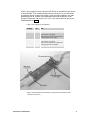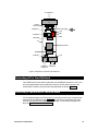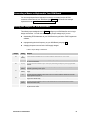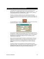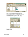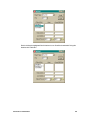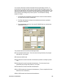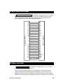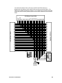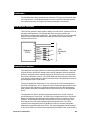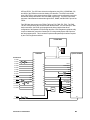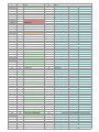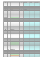
1
2608 Sweetgum Drive
Apex NC 27502
Toll-free: 800-549-9377
International: 919-387-0076
FAX: 919-387-1302
XSA Board V1.0
User Manual
How to install, test, and use
your new XSA Board
RELEASE DATE: 9/14/2001
Copyright © 2001 by X Engineering Software Systems Corporation.
All XS-prefix product designations are trademarks of XESS Corp.
All XC-prefix product designations are trademarks of Xilinx.
All rights reserved. No part of this publication may be reproduced, stored in a retrieval
system, or transmitted, in any form or by any means, electronic, mechanical,
photocopying, recording, or otherwise, without the prior written permission of the publisher.
Printed in the United States of America.
XSA BOARD V1.0 USER MANUAL
1
Table of Contents
Table of Contents................................................................................................2
Preliminaries........................................................................................................4
Getting Help!.................................................................................................4
Take notice!! .................................................................................................4
Packing List ..................................................................................................5
Installation............................................................................................................6
Installing the XSTOOLS Utilities and Documentation ................................6
Applying Power to Your XSA Board............................................................6
Using a 9VDC wall-mount power supply ....................................................6
Powering Through the PS/2 Connector ......................................................6
Solderless Protoboard Installation...............................................................6
Connecting a PC to Your XSA Board .........................................................8
Connecting a VGA Monitor to Your XSA Board .........................................8
Connecting a Mouse or Keyboard to Your XSA Board..............................9
Setting the Jumpers on Your XSA Board ...................................................9
Testing Your XSA Board............................................................................10
Programming the XSA Board Clock Oscillator .........................................11
Programming.....................................................................................................12
Downloading Designs into the FPGA and CPLD of Your XSA Board ....12
Storing Non-Volatile Designs in Your XSA Board ....................................15
Downloading and Uploading Data to the SDRAM in Your XSA Board...17
Programmer's Models.......................................................................................19
XSA Board Organization............................................................................19
Programmable logic: XC2S100 Spartan-II FPGA and XC9572XL CPLD20
100 MHz Programmable Oscillator ...........................................................20
XSA BOARD V1.0 USER MANUAL
2
16 MByte Synchronous DRAM .................................................................22
256 KByte Flash RAM................................................................................22
Seven-Segment LED .................................................................................24
Four-Position DIP Switch...........................................................................24
PS/2 Port.....................................................................................................24
Pushbutton..................................................................................................25
VGA Monitor Interface ...............................................................................25
Parallel Port Interface.................................................................................25
XSA Pin Connections .......................................................................................27
XSA Schematics ...............................................................................................28
XSA BOARD V1.0 USER MANUAL
3
1
Preliminaries
Getting Help!
Here are some places to get help if you encounter problems:
If you can't get the XSA Board hardware to work, send an e-mail message describing
your problem to [email protected] or submit a problem report at
http://www.xess.com/reqhelp.html. Our web site also has
answers to frequently-asked-questions,
example designs for the XS Boards,
application notes,
a place to sign-up for our email forum where you can post questions to other XS
Board users.
If you can't get your Xilinx WebPACK software tools installed properly, send an e-mail
message describing your problem to [email protected] or check their web site at
http://www.xilinx.com/support/support.htm.
Take notice!!
The XSA Board requires an external power supply to operate! It does not draw power
through the downloading cable from the PC parallel port.
If you are connecting a 9VDC power supply to your XSA Board, please make sure the
center terminal of the plug is positive and the outer sleeve is negative.
XSA BOARD V1.0 USER MANUAL
4
Packing List
Here is what you should have received in your package:
an XSA Board;
a 6' cable with a 25-pin male connector on each end;
an XSTOOLS CDROM with software utilities and documentation for using the XSA
Board.
XSA BOARD V1.0 USER MANUAL
5
2
Installation
Installing the XSTOOLS Utilities and Documentation
Xilinx currently provides the WebPACK tools for programming their CPLDs and Spartan-II
FPGAs. Any recent version of WebPACK software should generate bitstream
configuration files that are compatible with your XSA Board. You can download the most
current version of the WebPACK tools from
http://www.xilinx.com/xlnx/xil_prodcat_landingpage.jsp?title=ISE+WebPack. Follow the
directions Xilinx provides for installing their software.
XESS Corp. provides the additional XSTOOLS utilities for interfacing a PC to your XSA
Board. Run the SETUP.EXE program on the XSTOOLS CDROM to install these utilities.
Applying Power to Your XSA Board
You can use your XSA Board in three ways, distinguished by the method you use to apply
power to the board.
Using a 9VDC wall-mount power supply
You can use your XSA Board all by itself to experiment with logic designs. Just place the
XSA Board on a non-conducting surface as shown in Figure 1. Then apply power to jack
J5 of the XSA Board from a 9V DC wall-mount power supply with a 2.1 mm female,
center-positive plug. (See Figure 2 for the location of jack J5 on your XSA Board.) The
on-board voltage regulation circuitry will create the voltages required by the rest of the
XSA Board circuitry. Be careful!! The voltage regulators on the XSA Board will
become hot. Attach a heat sink to them if necessary.
Powering Through the PS/2 Connector
You can use your XSA Board with a laptop PC by connecting a PS/2 male-to-male cable
from the PS/2 port of the laptop to the J4 connector. You must also have a shunt across
pins 1 and 2 of jumper J7. The on-board voltage regulation circuitry will create the
voltages required by the rest of the XSA Board circuitry. Many PS/2 ports cannot
supply more than 0.5A so large, fast FPGA designs may not work when using
this power source!
Solderless Protoboard Installation
The two rows of pins from your XSA Board can be plugged into a solderless protoboard
with holes spaced at 0.1" intervals. (One of the A.C.E. protoboards from 3M is a good
XSA BOARD V1.0 USER MANUAL
6
choice.) Once plugged in, many of the pins of the FPGA are accessible to other circuits
on the protoboard. (The numbers printed next to the rows of pins on your XSA Board
correspond to the pin numbers of the FPGA.) Power can still be supplied to your XSA
Board though jack J9, or power can be applied directly through several pins on the
underside of the board. Just connect +5V, +3.3V, +2.5V and ground to the pins of your
XSA Board listed in Table 1.
• Table 1: Power supply pins for the XSA Board.
Voltage
Pin
+5V
2
+3.3V
22
Note
Remove the shunt from jumper J7 if you wish
to use your own +3.3V supply.
Leave the shunt on jumper J7 to generate the
+3.3V supply from the +5V supply.
+2.5V
54
Remove the shunt from jumper J2 if you wish
to use your own +2.5V supply.
Leave the shunt on jumper J2 to generate the
+2.5V supply from the +3.3V supply.
GND
52
• Figure 1: External connections to the XSA Board. (Actually, this is an XS40 Board, but the
connections are the same.)
XSA BOARD V1.0 USER MANUAL
7
PC Parallel Port
J8
External
Clock Input
J7
J9
100 MHz Osc.
9VDC Power Supply
J6
+3.3V
GND
SW1
Pushbutton
U15
CPLD
Flash RAM
+5V
Spartan-II FPGA
U10
J10
J2
SDRAM
Pushbutton
+2.5V
SW2
J4
J3
PS/2 Mouse VGA Monitor
or Keyboard
• Figure 2: Arrangement of components on the XSA Board.
Connecting a PC to Your XSA Board
The 6' DB25 male-to-male cable included with your XSA Board connects it to a PC. One
end of the cable attaches to the parallel port on the PC and the other connects to the
female DB-25 connector (J8) at the top of the XSA Board as shown in Figure 1.
Connecting a VGA Monitor to Your XSA Board
You can display images on a VGA monitor by connecting it to the 15-pin J3 connector at
the bottom of your XSA Board (see Figure 1). You will have to download a VGA driver
circuit to your XSA Board to actually display an image. You can find an example VGA
driver at http://www.xess.com/ho03000.html.
XSA BOARD V1.0 USER MANUAL
8
Connecting a Mouse or Keyboard to Your XSA Board
You can accept inputs from a keyboard or mouse by connecting it to the J4 PS/2
connector at the bottom of your XSA Board (see Figure 1). You can find an example
keyboard driver at http://www.xess.com/ho03000.html.
Setting the Jumpers on Your XSA Board
The default jumper settings shown in Table 2 configure your XSA Board for use in a logic
design environment. You will need to change the jumper settings only if you are:
downloading FPGA bitstreams to your XSA Board using the Xilinx JTAG Programmer
software,
reprogramming the clock frequency on your XSA Board (see page 11),
changing the power sources for the XSA supply voltages.
• Table 2: Jumper settings for XSA Boards.
Jumper
Setting
Purpose
J2
On
(default)
A shunt should be installed if the +2.5V supply voltage is derived from the +3.3V supply.
J6
J7
Off
The shunt should be removed if the +2.5V supply voltage is applied from an external source through
pin 22 of the XSA Board.
1-2 (set)
The shunt should be installed on pins 1 and 2 (set) when setting the frequency of the programmable
oscillator.
2-3 (osc)
(default)
The shunt should be installed on pins 2 and 3 (osc) during normal operations when the programmable
oscillator is generating a clock signal.
1-2
(default)
The shunt should be installed on pins 1 and 2 if the +3.3V supply voltage is derived from the +5V
supply.
2-3
J9
J10
The shunt should be installed on pins 2 and 3 if the +3.3V supply voltage is derived from the 9VDC
supply applied through jack J5.
1-2 (xi)
The shunt should be installed on pins 1-2 if the XSA Board is to be downloaded using the Xilinx JTAG
Programmer software utility.
2-3 (xs)
(default)
The shunt should be installed on pins 2-3 if the XSA Board is to be downloaded using the XESS
GXSLOAD software utility.
N/A
This is a header that provides access to the +5V and GND references on the board. No shunt should
be placed on this header.
XSA BOARD V1.0 USER MANUAL
9
Testing Your XSA Board
Once your XSA Board is installed and the jumpers are in their default configuration, you
can test the board using the GUI-based GXSTEST utility as follows.
You start GXSTEST by clicking on the
icon placed on the desktop during the
XSTOOLS installation. This brings up the screen shown below.
Next you select the parallel port that your XS Board is connected to from the Port pulldown
list. GXSTEST starts with parallel port LPT1 as the default, but you can also select LPT2
or LPT3 depending upon the configuration of your PC.
After selecting the parallel port, you select the type of XS Board you are testing from the
associated pulldown list. Then click on the TEST button to start the testing procedure.
GXSTEST will configure the FPGA to perform a test procedure on your XSA Board. After
several seconds you will see a O displayed on the LED digit if the test completes
successfully. Otherwise an E will be displayed if the test fails. A status window will also
appear on your PC screen informing you of the success or failure of the test.
If your XS Board fails the test, you will be shown a checklist of common causes for failure.
If none of these causes applies to your situation, then test the board using another PC. In
our experience, 99.9% of all problems are due to the parallel port. If you cannot get your
board to pass the test even after taking these steps, then contact XESS Corp for further
assistance.
As a result of testing the XSA Board, the CPLD is programmed with the standard parallel
port interface found in the dwnldpar.svf bitstream file located within the XSTOOLS\XSA
folder. This is the standard interface that should be loaded into the CPLD when you want
to use it with the GXSLOAD utility.
XSA BOARD V1.0 USER MANUAL
10
Programming the XSA Board Clock Oscillator
The XSA Board has a 100 MHz programmable oscillator (a Dallas Semiconductor
DS1075Z-100). The 100 MHz master frequency can be divided by factors of 1, 2, ... up to
2052 to get clock frequencies of 100 MHz, 50 MHz, ... down to 48.7 KHz, respectively.
The divided frequency is sent to the FPGA as a clock signal.
The divisor is stored in non-volatile memory in the oscillator chip so it will resume
operation at its programmed frequency whenever power is applied to the XS Board. You
can store a particular divisor into the oscillator chip by using the GUI-based GXSSETCLK
as follows.
You start GXSSETCLK by clicking on the
icon placed on the desktop during
the XSTOOLS installation. This brings up the screen shown below.
Your next step is to select the parallel port that your XSA Board is connected to from the
Port pulldown list. GXSSETCLK starts with parallel port LPT1 as the default, but you can
also select LPT2 or LPT3 depending upon the configuration of your PC. After selecting
the parallel port, you select from the pulldown list the type of XS Board you have
connected to the PC parallel port.
Next you must enter a divisor between 1 and 2052 into the Divisor text box. Once it is
programmed, the oscillator will output a clock signal generated by dividing its 100 MHz
master frequency by the divisor. The divisor is stored in non-volatile storage in the
oscillator chip so you only need to use GXSSETCLK when you want to change the
frequency.
An external clock signal can be substituted for the internal master frequency of the
programmable oscillator. Checking the external clock checkbox will enable this feature in
the programmable oscillator chip. If the external clock option is selected, you are then
responsible for providing the external clock to the XSA Board through pin 64.
XSA BOARD V1.0 USER MANUAL
11
3
Programming
This section will show you how to download a logic designs into the FPGA and CPLD of
your XSA Board and how to download and upload data to and from the SDRAM and
Flash devices on the board.
Downloading Designs into the FPGA and CPLD of Your XSA Board
During the development and testing phases, you will usually connect the XSA Board to the
parallel port of a PC and download your circuit each time you make changes to it. You
can download a Spartan-II FPGA design into your XSA Board using the GXSLOAD utility
as follows.
You start GXSLOAD by clicking on the
icon placed on the desktop during the
XSTOOLS installation. Then select the type of XS Board you are using and the parallel
port to which it is connected as shown below.
After setting the board type and parallel port, you can download .BIT or .SVF files to the
Spartan-II FPGA or XC9572XL CPLD on your XSA Board simply by dragging them to the
FPGA/CPLD area of the GXSLOAD window as shown below.
XSA BOARD V1.0 USER MANUAL
12
Once you release the left mouse button and drop the file, the highlighted file name
appears in the FPGA/CPLD area and the Load button in the GXSLOAD window is
enabled. Clicking on the Load button will begin sending the highlighted file to the XSA
Board through the parallel port connection. .BIT files contain configuration bitstreams that
are loaded into the FPGA while .SVF files will go to the CPLD. GXSLOAD will reject any
non-downloadable files (ones with a suffix other than .BIT or .SVF). During the
downloading process, GXSLOAD will display the name of the file and the progress of the
current download.
You can drag & drop multiple files into the FPGA/CPLD area. Clicking your mouse on a
filename will highlight the name and select it for downloading. Only one file at a time can
be selected for downloading.
XSA BOARD V1.0 USER MANUAL
13
Double-clicking the highlighted file will deselect it so no file will be downloaded Doing this
disables the Load button.
XSA BOARD V1.0 USER MANUAL
14
Storing Non-Volatile Designs in Your XSA Board
The Spartan-II FPGA on the XSA Board stores its configuration in an on-chip SRAM
which is erased whenever power is removed. Once your design is finished, you may want
to store the bitstream in the 256 KByte Flash device on the XSA Board which configures
the FPGA for operation as soon as power is applied.
Before downloading to the Flash, the FPGA .BIT file must be converted into a .EXO or
.MCS format using one of the following commands:
promgen –u 0 file.bit –p exo –s 256
promgen –u 0 file.bit –p mcs –s 256
In the commands shown above, the bitstream in the file.bit file is transformed into an .EXO
or .MCS file format starting at address zero and proceeding upward until an upper limit of
256 KBytes is reached.
Before attempting to program the Flash, you must place all four DIP switches
into the OFF position!
After the .EXO or .MCS file is generated, it is loaded into the Flash device by dragging it
into the Flash/EEPROM area and clicking on the Load button. This activates the following
sequence of steps:
1. The entire Flash device is erased.
2. The CPLD on the XSA Board is reprogrammed to create an interface between
the Flash device and the PC parallel port. (This interface is stored in the
fintf100.svf bitstream file located within the XSTOOLS\XSA folder.)
3. The contents of the .EXO or .MCS file are downloaded into the Flash through the
parallel port.
4. The CPLD is reprogrammed to create a circuit that configures the FPGA with the
contents of the Flash when power is applied to the XSA Board. (This
configuration loader is stored in the fcnfg100.svf bitstream file located within the
XSTOOLS\XSA folder.)
Multiple files can be stored in the Flash device just by dragging them into the
Flash/EEPROM area, highlighting the files to be downloaded and clicking the Load button.
(Note that anything previously stored in the Flash will be erased by each new download.)
This is useful if you need to store information in the Flash in addition to the FPGA
bitstream. Files are selected and de-selected for downloading just by clicking on their
names in the Flash/EEPROM area. The address ranges of the data in each file
should not overlap or this will corrupt the data stored in the Flash device!
XSA BOARD V1.0 USER MANUAL
15
You can also examine the contents of the Flash device by uploading it to the PC. To
upload data from an address range in the Flash, type the upper and lower bounds of the
range into the High Address and Low Address fields below the Flash/EEPROM area, and
select the format in which you would like to store the data using the drop-down list. Then
click on the file icon and drag & drop it into any folder. This activates the following
sequence of steps:
1. The CPLD on the XSA Board is reprogrammed to create an interface between
the Flash device and the PC parallel port.
2. The Flash data between the high and low addresses (inclusive) is uploaded
through the parallel port.
3. The uploaded data is stored in a file named FLSHUPLD with an extension that
reflects the file format.
The uploaded data can be stored in the following formats:
MCS: Intel hexadecimal file format. This is the same format generated by the promgen
utility with the –p mcs option.
HEX: Identical to MCS format.
EXO-16: Motorola S-record format with 16-bit addresses (suitable for 64 KByte uploads
only).
EXO-24: Motorola S-record format with 24-bit addresses. This is the same format
generated by the promgen utility with the –p exo option.
EXO-32: Motorola S-record format with 32-bit addresses.
XES-16: XESS hexadecimal format with 16-bit addresses. (This is a simplified file format
that does not use checksums.)
XES-24: XESS hexadecimal format with 24-bit addresses.
XSA BOARD V1.0 USER MANUAL
16
XES-32: XESS hexadecimal format with 32-bit addresses.
After the data is uploaded from the Flash, you must reprogram the CPLD on the XSA
Board with one of the following files:
XSTOOLS\XSA\fintf100.svf: Drag & drop this file into the FPGA/CPLD area and click on
the Load button to put the XSA in a mode where it will configure the FPGA with the
contents of the Flash device upon power-up.
XSTOOLS\XSA\dwnldpar.svf: Drag & drop this file into the FPGA/CPLD area and click on
the Load button to put the XSA in a mode where it will configure the FPGA through
the parallel port.
Downloading and Uploading Data to the SDRAM in Your XSA Board
The XSA Board contains a 16 MByte synchronous DRAM (SDRAM) whose contents can
be downloaded and uploaded by GXSLOAD. This is useful for initializing the SDRAM with
data for use by the FPGA and then reading the SDRAM contents after the FPGA has
operated upon it. The SDRAM is loaded with data by dragging & dropping one or more
.EXO, .MCS, .HEX, and/or .XES files into the RAM area of the GXSLOAD window and
then clicking on the Load button. This activates the following sequence of steps:
1. The Spartan-II FPGA on the XSA Board is reprogrammed to create an interface
between the RAM device and the PC parallel port. (This interface is stored in the
ram100.bit bitstream file located within the XSTOOLS\XSA folder. The CPLD
must have previously been loaded with the dwnldpar.svf file found in
the same folder.)
2.
The contents of the .EXO, .MCS, .HEX or .XES files are downloaded into the
SDRAM through the parallel port. The data in the files will overwrite each
other if their address ranges overlap.
3. If any file is highlighted in the FPGA/CPLD area, then this bitstream is loaded into
the FPGA or CPLD on the XSA Board. Otherwise the FPGA remains configured
as an interface to the SDRAM.
You can also examine the contents of the SDRAM device by uploading it to the PC. To
upload data from an address range in the SDRAM, type the upper and lower bounds of
the range into the High Address and Low Address fields below the RAM area, and select
the format in which you would like to store the data using the drop-down list. Then click on
the file icon and drag & drop it into any folder. This activates the following sequence of
steps:
1. The Spartan-II FPGA on the XSA Board is reprogrammed to create an interface
between the RAM device and the PC parallel port. (This interface is stored in the
ram100.bit bitstream file located within the XSTOOLS\XSA folder.)
2. The SDRAM data between the high and low addresses (inclusive) is uploaded
through the parallel port.
3. The uploaded data is stored in a file named RAMUPLD with an extension that
reflects the file format.
XSA BOARD V1.0 USER MANUAL
17
XSA BOARD V1.0 USER MANUAL
18
4
Programmer's
Models
This section describes the various sections of the XSA Board and shows how the I/O of
the FPGA and CPLD are connected to the rest of the circuitry. The schematics which
follow are less detailed so as to simplify the descriptions. Please refer to the complete
schematics at the end of this document if you need more details.
XSA Board Organization
The XSA Board contains the following components:
XC2S100 Spartan-II FPGA: This is the main repository of programmable logic on the XSA
Board.
XC9572XL CPLD: This CPLD manages the interfaces between the PC parallel port and
the rest of the XSA Board.
Osc: A programmable oscillator generates the master clock for the XSA Board.
Flash: A 256 KByte Flash device provides non-volatile storage for data and configuration
bitstreams.
SDRAM: A 16 MByte SDRAM provides volatile storage for data accessible by the FPGA.
LED: A seven-segment LED allows visible feedback as the XSA Board operates.
DIP switch: A four-position DIP switch passes settings to the XSA Board or controls the
upper address bits of the Flash device.
Pushbutton: A single pushbutton sends momentary contact information to the FPGA.
Parallel Port: This is the main interface for passing configuration bitstreams and data to
and from the XSA Board.
PS/2 Port: A keyboard or mouse can interface to the XSA Board through this port.
VGA Port: The XSA Board can send signals to display graphics on a VGA monitor through
this port.
Prototyping Header: Many of the FPGA I/O pins are connected to the 84 pins on the
bottom of the XSA Board that are meant to mate with solderless breadboards.
XSA BOARD V1.0 USER MANUAL
19
D7-D0
A17-A0
8
Parallel Port
2 - PPD0
3 - PPD1
4 - PPD2
5 - PPD3
6 - PPD4
7 - PPD5
8 - PPD6
9 - PPD7
17 - PPC3
16 - PPC2
14 - PPC1
11 - PPS7
12 - PPS5
13 - PPS4
15 - PPS3
/WE
/RESET
/CE
/OE
FLASH
XC9572XL
XC2S100
A17 - A0
D7 - D0
D7-D0
D15 - D0
SDRAM
BA1 - BA0, A12 - A0
RAS, CAS, /CS, /WE
TDI
TMS
TCK
TDO
GCLK
OSC
CCLK
/PROGRAM
/INIT
M0
GCLK
M1
M2
/CS
/WR
BSY/DOUT
DONE
TCK
TMS
TDI
TDO
GCLK
1 - PPC0
10 - PPS6
DQMH
DQML
CKE
CLK
PS/2 Port
PSCLK
PSDATA
RED1 - RED0
GREEN1 - GREEN0
BLUE1 - BLUE0
/HSYNC
/VSYNC
VGA Connector
• Figure 3: XSA Board programmer’s model.
Programmable logic: XC2S100 Spartan-II FPGA and XC9572XL CPLD
The XSA Board contains two programmable logic chips:
A 100-Kgate Xilinx XC2S100 Spartan-II FPGA in a 144-pin QFP package. The FPGA
is the main repository of programmable logic on the XSA Board.
A Xilinx XC9572XL CPLD that is used to manage the configuration of the FPGA via
the parallel port. The CPLD also controls the programming of the Flash RAM on the
XSA Board.
100 MHz Programmable Oscillator
A Dallas DS1075 programmable oscillator provides a clock signal to both the FPGA and
the CPLD. The DS1075 has a maximum frequency of 100 MHz that is divided to provide
frequencies of 100 MHz, 50 MHz, 33.3 MHz, 25 MHz, ..., 48.7 KHz. The clock signal is
connected to a dedicated clock input of the CPLD. The CPLD passes the clock signal on
to the FPGA. This allows the CPLD to control the clock source for the FPGA.
To set the divisor value, the DS1075 must be placed in its programming mode. This is
done by pulling the clock output to +5V on power-up with a shunt across pins 1 and 2 of
jumper J6. Then programming commands to set the divisor can be sent to the DS1075
XSA BOARD V1.0 USER MANUAL
20
control pin C0 of the parallel port. The divisor is stored in EEPROM in the DS1075 so it
will be restored whenever power is applied to the XSA Board.
The shunt on jumper J6 must be across pins 2 and 3 to make the oscillator output a clock
signal upon power-up. The clock signal enters a dedicated clock input of the CPLD. Then
the CPLD can output a clock signal to a dedicated clock input of the FPGA.
To get a precise frequency value or to sync the XSA circuitry with an external system, you
can insert an external clock signal through pin 64 of the prototyping header. This external
clock replaces the internal 100 MHz clock source in the DS1075 oscillator. You must use
the GXSSETCLK software utility to enable the external clock input of the DS1075.
Clock signals can also be directly applied to two of the dedicated clock inputs of the FPGA
through the pins of the prototyping header.
+5V
PP-C0
J6
Pin 1
18
88
Spartan-II
FPGA
Pin 31
42
17
XC9572XL
CPLD
1
2
3
DS1075
Pin 64
100 MHz
Prog. Osc.
15
XSA BOARD V1.0 USER MANUAL
21
16 MByte Synchronous DRAM
95
99
101
103
113
115
117
120
121
118
116
114
112
102
100
96
141
4
6
10
11
7
5
3
140
138
139
136
133
134
137
123
132
130
126
124
122
131
129
91
Q0
Q1
Q2
Q3
Q4
Q5
Q6
Q7
Q8
Q9
Q10
Q11
Q12
Q13
Q14
Q15
A0
A1
A2
A3
A4
A5
A6
A7
A8
A9
A10
A11
A12
BA0
BA1
/WE
/CS
/RAS
/CAS
DQMH
DQML
CKE
CLK
8M X 16 SDRAM
Spartan-II FPGA
A Hynix HY57V281620AT-H SDRAM with 16 MBytes of storage (8M × 16) is connected to
the FPGA as shown below. Note that the clock signal to the SDRAM is also re-routed
back to a dedicated clock input of the FPGA. This makes it easy to synchronize the
internal operations of the FPGA with the SDRAM operations.
256 KByte Flash RAM
An Atmel AT49F002 Flash RAM with 256 KBytes of storage (256K × 8) is connected to
both the FPGA and CPLD as shown below.
The CPLD and FPGA both have access to the Flash RAM. Typically, the CPLD will
program the Flash with data passed through the parallel port. If the data is an FPGA
configuration bitstream, then the CPLD can be configured to program the FPGA with the
bitstream from Flash whenever the XSA Board is powered up. After power-up, the FPGA
XSA BOARD V1.0 USER MANUAL
22
can read and/or write the Flash. (Of course, the CPLD and FPGA have to be
programmed such that they do not conflict if both are trying to access the Flash.) The
Flash can be disabled by raising the /CE pin to +5V in which case the I/O lines connected
to the Flash can be used for general-purpose communication between the FPGA and the
CPLD.
11
12
49
50
1
64
63
62
61
60
59
58
45
44
57
43
56
46
47
52
51
48
2
4
5
6
7
8
9
10
41
43
58
59
40
29
28
27
74
75
76
66
50
48
42
47
65
51
54
64
63
56
39
44
46
49
57
60
62
67
+5V
S6
8
S5
S4
S2 S3 S1
S0
DP
DIPSW1
DIPSW2
DIPSW3
DIPSW4
S0
S2
S3
S5
S6
S4
DP
S1
Spartan-II FPGA
XC9572XL CPLD
/CE
/OE
/WE
/RESET
A0
A1
A2
A3
A4
A5
A6
A7
A8
A9
A10
A11
A12
A13
A14
A15
A16
A17
D0
D1
D2
D3
D4
D5
D6
D7
256 KByte Flash RAM
XSA BOARD V1.0 USER MANUAL
23
Seven-Segment LED
The XSA Board has a 7-segment LED digit for use by the FPGA or the CPLD. The
segments of this LED are active-high meaning that a segment will glow when a logic-high
is applied to it.
The LED shares the same pins as the eight bits of the Flash RAM data bus.
Four-Position DIP Switch
The XSV Board has a bank of four DIP switches accessible from the CPLD and FPGA.
When closed or ON, each switch pulls the connected pin of the FPGA and CPLD to
ground. Otherwise, the pin is pulled high through a resistor when the switch is open or
OFF.
When not being used, the DIP switches should be left in the open or OFF
configuration so the pins of the FPGA and CPLD are not tied to ground and can
freely move between logic low and high levels.
The DIP switches also share the same pins as the uppermost four bits of the Flash RAM
address bus. If the Flash RAM is programmed with several FPGA bitstreams, then the
DIP switches can be used to select a particular bitstreams which will be loaded into the
FPGA by the CPLD on power-up.
PS/2 Port
The XSA Board provides a PS/2-style interface (mini-DIN connector J4) to either a
keyboard or a mouse. The FPGA receives two signals from the PS/2 interface: a clock
signal and a serial data stream that is synchronized with the falling edges on the clock
signal.
+5V
Spartan-II
FPGA
94
93
clk
data
PS/2
Connector
(J4)
Pushbutton
(SW2)
XSA BOARD V1.0 USER MANUAL
24
Pushbutton
The XSA Board has a single pushbutton that shares the FPGA pin connected to the data
line of the PS/2 port. The pushbutton applies a low level to the FPGA pin when pressed
and a resistor pulls the pin to a high level when the pushbutton is not pressed.
VGA Monitor Interface
The FPGA can generate a video signal for display on a VGA monitor. When the FPGA is
generating VGA signals, the FPGA outputs two bits of red, green, and blue color
information to a simple resistor-ladder DAC. The outputs of the DAC are sent to the RGB
inputs of a VGA monitor along with the horizontal and vertical sync pulses (/HSYNC,
/VSYNC) from the FPGA.
vsync
26
23
12
Spartan-II
FPGA
13
19
20
21
22
RED0
RED1
hsync
red
GREEN0
GREEN1
green
VGA
Connector
(J3)
BLUE0
BLUE1
blue
Parallel Port Interface
The parallel port is the main interface for communicating with the XSA Board. Control line
C0 goes directly to the DS1075 oscillator and is used for setting the divisor as described
previously, and status line S6 connects directly to the FPGA for use as a communication
line from the FPGA back to the PC. The CPLD handles the fifteen remaining active lines
of the interface to the parallel port. Fifteen of the active lines of the parallel port connect to
general-purpose I/O pins on the CPLD.
Three of the parallel port control lines, C1–C3, connect to the JTAG pins through which
the CPLD is programmed. The C1 control line clocks configuration data presented on the
C3 line into the CPLD while the C2 signal steers the actions of the CPLD programming
state machine. Meanwhile, information from the CPLD returns to the PC through status
line S7.
The eight data lines, D0–D7, and the remaining three status lines, S3–S5, connect to
general-purpose pins of the CPLD. The CPLD can be programmed to act as an interface
between the FPGA and the parallel port (the dwnldpar.svf file is an example of such an
interface). Schmitt-trigger inverters are inserted into the D1 line so it can carry a clean
clock edge for use by any state machine programmed into the CPLD. The CPLD
connects to the configuration pins of the Spartan-II FPGA so it can pass configuration
bitstreams from the parallel port to the FPGA. The actual configuration data is presented
on the to the FPGA on the same 8-bit bus that connects the CPLD, Flash, seven-segment
XSA BOARD V1.0 USER MANUAL
25
LED and FPGA. The CPLD also drives the configuration pins (CCLK, /PROGRAM, /CS,
and /WR) of the FPGA that control the loading of a bitstream. The CPLD uses the M0
input of the FPGA to select either the slave-serial or master-select configuration mode (M1
and M2 are already hard-wired to VCC and GND, respectively.) The CPLD can monitor
the status of the bitstream download through the /INIT, DONE, and BSY/DOUT pins of the
FPGA.
The CPLD also has access to the FPGA JTAG pins: TCK, TMS, TDI, TDO. The TMS,
TDI, and TDO pins share the connections with the BSY/DOUT, /CS, and /WR pins. With
these connections, the CPLD can be programmed with an interface that allows
configuration of the Spartan-II FPGA through the Xilinx JTAG Programmer software utility.
Jumper J9 allows the connection of status pin S7 to the general-purpose CPLD pin that
also drives status pin S5. This is needed to implement the parallel port interface required
by the JTAG Programmer software.
FLASH RAM
8
XC9572XL
Spartan-II FPGA
Parallel Port
D7 - D0
2 - PPD0
33
3 - PPD1
32
4 - PPD2
31
5 - PPD3
27
6 - PPD4
25
7 - PPD5
24
8 - PPD6
23
9 - PPD7
17 - PPC3
TDI
16 - PPC2
TMS
14 - PPC1
TCK
11 - PPS7
TDO
/PROGRAM
39
/INIT
38
M0
36
M1
22
M2
28
/CS
29
30
53
12 - PPS5
35
13 - PPS4
20
15 - PPS3
34
1 - PPC0
CCLK
16
15
/WR
19
BSY/DOUT
18
DONE
40
TCK
13
TMS
OSC
TDI
TDO
37
69
68
109
31
30
38
72
2
142
32
34
78
10 - PPS6
XSA BOARD V1.0 USER MANUAL
26
A
XSA Pin Connections
The following tables list the pin numbers of the Spartan-II FPGA and the XC9572XL CPLD
along with the pins of the other chips that they connect to on the XSA Board. The
columns of the table are arranged as follows:
Column 1 lists the Spartan-II FPGA pin. It is left blank if there is no connection to the
FPGA for this function.
Column 2 lists the XC9572XL CPLD pin. It is left blank if there is no connection to the
CPLD for this function.
Column 3 lists the pins of other devices on the XSA Board that are connected to the
associated FPGA and/or CPLD port.
Column 4 lists the pin of the XSA prototyping header that is connected to the associated
FPGA and/or CPLD pin.
Columns 5–7 list the pins of devices on the Xstend Board that will connect to the FPGA
and/or CPLD when the XSA Board is inserted into an Xstend Board.
XSA BOARD V1.0 USER MANUAL
27
FPGA
1
2
3
4
5
6
7
8
9
10
11
12
13
15
18
19
20
21
22
23
26
27
28
29
30
31
32
34
37
38
39
40
41
42
43
44
46
47
48
49
50
51
54
56
57
58
59
60
62
63
64
65
66
67
68
69
72
74
75
76
77
78
79
CPLD XSA Function
+3.3V
13
SPARTAN-TCK
SDRAM-A7
SDRAM-A1
SDRAM-A6
SDRAM-A2
SDRAM-A5
GND
+2.5V
SDRAM-A3
SDRAM-A4
VGA-RED0
VGA-RED1
SPARTAN-GCK3
SPARTAN-GCK2
VGA-GREEN0
VGA-GREEN1
VGA-BLUE0
VGA-BLUE1
VGA-/HSYNC
VGA-/VSYNC
62
FLASH-A3
63
FLASH-A2
64
FLASH-A1
19
SPARTAN-/WRITE
15
SPARTAN-CS
15*
SPARTAN-TDI
19*
SPARTAN-TDO
16
SPARTAN-CCLK
18
SPARTAN-DOUT/BSY
2
FLASH-D0,DIN/D0,LED-S1
1
FLASH-A0
11
FLASH-/CE
57
FLASH-A10
12
FLASH-/OE
4
FLASH-D1,LED-DP
5
FLASH-D2,LED-S4
43
FLASH-A11
44
FLASH-A9
6
FLASH-D3,LED-S6
45
FLASH-A8
46
FLASH-A13
47
FLASH-A14,DIPSW1A
48
FLASH-A17,DIPSW1D
7
FLASH-D4,LED-S5
49
FLASH-/WE
50
FLASH-/RESET
8
FLASH-D5,LED-S3
9
FLASH-D6,LED-S2
51
FLASH-A16,DIPSW1C
52
FLASH-A15,DIPSW1B
56
FLASH-A12
58
FLASH-A7
10
FLASH-D7,LED-S0
38
SPARTAN-/INIT
39
SPARTAN-/PROGRAM
40
SPARTAN-DONE
61
FLASH-A4
60
FLASH-A5
59
FLASH-A6
PARPORT-S6
Proto. Pin
54
16
52
22
27
28
31
1
29
32
33
34
36
37
50
51
56
69
68
15
30
73
45
71
57
65
58
61
40
39
59
60
38
78
79
82
83
35
62
66
80
81
84
3
4
5
10
41
55
53
70
77
6
9
67
7
XSTend Functions
+3.3V
Xchecker-TCK
GND
RAM-A15
RLED-/DP
Xchecker-RT
RAM-A12
RAM-A10
RAM-A11
PS2/DATA
PS2/CLK
Pushbutton-/RESET
RLED-/S4
RLED-/S2
RLED-/S3
DIPSW8
Xchecker-TDI
Xchecker-RD
Xchecker-CCLK
Xchecker-DIN
RAM-A9
RLED-/S1
RAM-/CE
RAM-A13
RLED-/S5
RAM-/OE
RAM-D1
BARLED-2
RAM-D2
BARLED-3
RAM-A8
RLED-/S0
RAM-A14
RLED-/S6
RAM-D3
BARLED-4
RAM-A3
LLED-/S3
RAM-A4
LLED-/S4
RAM-A5
LLED-/S5
RAM-A6
LLED-/S6
RAM-D4
BARLED-5
RAM-WE
CODEC-LRCK
DIPSW7
RAM-D6
BARLED-7
RAM-D5
BARLED-6
RAM-A7
LLED-/DP
RAM-A0
LLED-/S0
RAM-A1
LLED-/S1
RAM-A2
LLED-/S2
RAM-D7
BARLED-8
RAM-D0
BARLED-1
Xchecker-INIT
Pushbutton-/PROGRAM Xchecker-PROG
Xchecker-DONE
CODEC-SDIN
DIPSW6
CODEC-SCLK
DIPSW5
CODEC-SDOUT DIPSW4
CODEC-MCLK
DIPSW3
Xchecker-CLKO
VGA-/VSYNC
Pushbutton-/SPARE
RAM-/LCE
DIPSW1
Xchecker-TRIG
FPGA
80
83
84
85
86
87
88
91
93
94
95
96
99
100
101
102
103
106
109
111
112
113
114
115
116
117
118
120
121
122
123
124
126
129
130
131
132
133
134
136
137
138
139
140
141
142
CPLD XSA Function
42
36
18*
30
29
28
33
32
31
27
25
24
23
22
34
20
35
53
17
MASTER_CLK
SDRAM-CLK
PS2-DATA,PUSHBUTTON
PS2-CLK
SDRAM-Q0
SDRAM-Q15
SDRAM-Q1
SDRAM-Q14
SDRAM-Q2
SDRAM-Q13
SDRAM-Q3
SPARTAN-M2
SPARTAN-M0
SPARTAN-M1
SDRAM-Q12
SDRAM-Q4
SDRAM-Q11
SDRAM-Q5
SDRAM-Q10
SDRAM-Q6
SDRAM-Q9
SDRAM-Q7
SDRAM-Q8
SDRAM-QML
SDRAM-/WE
SDRAM-QMH
SDRAM-/CAS
SDRAM-CLK
SDRAM-/RAS
SDRAM-CKE
SDRAM-/CS
SDRAM-A12
SDRAM-BA0
SDRAM-A11
SDRAM-BA1
SDRAM-A9
SDRAM-A10
SDRAM-A8
SDRAM-A0
SPARTAN-TMS
PARPORT-C1,CPLD-TCK
PARPORT-C2,CPLD-TMS
PARPORT-C3,CPLD-TDI
PARPORT-D0
PARPORT-D1
PARPORT-D2
PARPORT-D3
PARPORT-D4
PARPORT-D5
PARPORT-D6
PARPORT-D7
PARPORT-S3
PARPORT-S4
PARPORT-S5
PARPORT-S7,CPLD-TDO
PROG-OSC
Proto. Pin
8
18
19
20
23
24
13
25
26
RAM-/RCE
VGA-RED1
VGA-/HSYNC
VGA-GREEN1
VGA-RED0
VGA-GREEN0
MASTER_CLK
XSTend Functions
DIPSW2
Xchecker-RST
Xchecker-CLKI
VGA-BLUE0
VGA-BLUE1
12
14
21
17
64
Xchecker-TMS
Osc-In
B
XSA Schematics
The following pages show the detailed schematics for the XSA Board.
XSA BOARD V1.0 USER MANUAL
28
xsa1_0.sch-1 - Tue Sep 11 15:53:20 2001
xsa1_0.sch-2 - Tue Sep 11 15:53:21 2001
xsa1_0.sch-3 - Tue Sep 11 15:53:21 2001
xsa1_0.sch-4 - Tue Sep 11 15:53:21 2001
xsa1_0.sch-5 - Tue Sep 11 15:53:22 2001
xsa1_0.sch-6 - Tue Sep 11 15:53:22 2001
xsa1_0.sch-7 - Tue Sep 11 15:53:22 2001
xsa1_0.sch-8 - Tue Sep 11 15:53:23 2001
xsa1_0.sch-9 - Tue Sep 11 15:53:23 2001