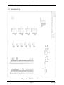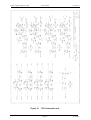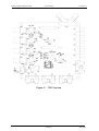
1
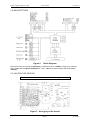
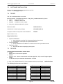
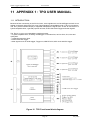
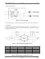
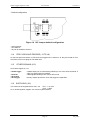
CMS Trigger Sequencer Card
User manual
version 3.0
CMS
Trigger Sequencer Card
User Manual
VERSION 3.0
Institut de Physique Nucléaire de Lyon
Page 1
July 2003
CMS Trigger Sequencer Card
User manual
version 3.0
1 Contents
1 CONTENTS
2
2 FIGURES
4
3 TABLES
4
4 INTRODUCTION
5
4.1 GENERAL DESCRIPTION
5
4.2 ARCHITECTURE
6
4.3 CAUTION FOR HEATING
6
5 HARDWARE
7
5.1 FRONT PANEL
7
5.2 INSIDE CONNECTORS
8
5.3 PCI
11
5.4 FPGA
11
5.5 EPROMs
11
5.6 DELAY LINES
11
5.7 JUMPERS & SWITCHES
12
5.8 BUTTONS
12
5.9 LEDS
13
5.10 SUPPLIES
13
6 TSC FUNCTIONALITIES
14
6.1 FONCTIONNAL BLOCK DIAGRAM
14
6.2
TRIGGER PART
14
6.2.1 TRIGGER SOURCE
14
6.2.2 TRIGGER FILTER
15
6.2.2.1 INHIBIT
15
6.2.2.2 GATE
15
6.2.2.3 MINIMUM NUMBER OF CLOCKS BETWEEN TRIGGERS
6.2.2.4 COUNTING
17
6.2.2.5 TRIGGER STAMP COUNTER AND FIFO 18
6.2.2.6 RESET TRIGGER FILTER
18
6.3
CLOCKS
18
6.4
SEQUENCER PART
18
6.4.1 TRIGGER SEQUENCE
18
6.4.2 CALIBRATION SEQUENCE
18
6.4.3 RESET SEQUENCE
19
6.4.4 FED CLOCK AND TRIGGER
19
6.5
ENCODER PART
19
6.6
PULSER
20
6.7
FIRMWARE
20
6.8
INTERRUPTS
20
6.9
RESETS
20
6.10 I2C BUSES
20
6.10.1 LOCAL I2C
20
6.10.2 EXTERNAL I2C
20
7 SOFTWARE
22
7.1 PCI CONFIGURATION AND ADDRESS MAP
22
7.1.1 MEMORY REQUIREMENTS
22
7.1.2 PCI CONFIGURATION REGISTERS
22
7.1.3 BRIDGE INITIALIZATION
23
7.2 I/O MAPPING
24
7.2.1 REGISTERS
25
7.3 SOFTWARE INSTALLATION
29
Page 2
17
July 2003
CMS Trigger Sequencer Card
User manual
7.4 DRIVER
29
7.5 DEVICE
29
7.6 USER LEVEL ROUTINES
30
8 GETTING STARTED
31
8.1 HARDWARE VERIFICATIONS
31
8.2 SOFTWARE TESTS
31
9 CONTACTS & ORDERING INFORMATION
31
10 VERSION AND HISTORY
31
11 APPENDIX 1 : TPO USER MANUAL
32
11.1 INTRODUCTION
11.2 HYBRID COMPATIBLE LINES (J11 TO J14)
11.3 GENERAL PURPOSE I2C LINES (J32, J18, J47 AND J48)
11.4 FED CLOCK AND TRIGGER ( J3 TO J8)
11.5 OTHER SIGNALS (J15)
11.6 SUPPLYING (J16)
11.7 SCHEMATICS
Page 3
version 3.0
32
33
33
35
35
35
36
July 2003
CMS Trigger Sequencer Card
User manual
version 3.0
2 FIGURES
Figure 1
Figure 2
Figure 3
Figure 4
Figure 5
Figure 6
Figure 7
Figure 8
Figure 9
Figure 10
Figure 11
Figure 12
Figure 13
Figure 14
Figure 15
Figure 16
Figure 17
Photograph of TSC
Block Diagram
Area (grey) to be fanned
Front panel connectors
Jumpers
Fonctionnal block diagram
Trigger gate timing
Trigger gate cabling
Trigger gate calibration
TPO Functionnal block diagram
I2C output jumper location
I2C output supply
I2C Cell functionnal diagram for J32
I2C Jumper default configuration
TPO Schematics no1
TPO Schematics no2
TPO Top view
3 TABLES
Table 1. Description of J8 local supply connector
Table 2. Description of JTAG connector
Table 3. Description of J1 connector
Table 4. Description of J2 connector
Table 5 Jumper settings
Table 6 LEDs
Table 7 Summary of the register address mapping
Table 8 Distribution of external I2C channels
Table 9 PCI bridge configuration registers
Table 10 Local bridge configuration registers
Table 11 Summary of the register address mapping
Table 12 Different jumper configurations for J32
Table 13 Summary of TPO connections
Page 4
July 2003
CMS Trigger Sequencer Card
User manual
version 3.0
4 INTRODUCTION
4.1 GENERAL DESCRIPTION
The TSC (Trigger Sequencer Card) is intended to assume timing aspects in the CMS silicon tracker
test stations.
It is presented in a PCI form factor for workstations (Figure 1).
Placed between trigger, clock source and FEC-CCU, it can also supply a laser pulser.
The trigger part assumes gating, counting and blocking following triggers. Internal clock and triggers
are also provided.
The sequencer part matches all APV requests including trigger, calibration and reset.
All the necessary software for TSC set up is provided.
Figure 1
Photograph of TSC
Page 5
July 2003
CMS Trigger Sequencer Card
User manual
version 3.0
4.2 ARCHITECTURE
Figure 2
Block Diagram
Main parts of this card include a PCI bridge to interface PCI bus, a FPGA for trigger logic, allowing
future modifications, biphase modulator for TTCrx, 2 DLLs for precise delays and several level
adaptors.
4.3 CAUTION FOR HEATING
Because of ECL use, this card produces heat. Fanning is mandatory.
Figure 3 Area (grey) to be fanned
Page 6
July 2003
CMS Trigger Sequencer Card
User manual
version 3.0
5 HARDWARE
5.1 FRONT PANEL
Figure 4. Front panel connectors
LED trigger accepted : highlights each time a trigger is accepted and sent to APVs.
FED clock and trigger (4x): LVDS clock and trigger outputs for FED(s).
Trigger input : NIM input for external trigger.
Pulser out : NIM output to trigger a pulser.
Reset Trigger Filter : NIM input for hardware Reset Trigger Filter.
Clock input : ECL external 40 Mhz clock input.
Optical output : Optical connection to the optical FEC input.
Page 7
July 2003
CMS Trigger Sequencer Card
User manual
version 3.0
5.2 INSIDE CONNECTORS
Local supply J8. For debugging. HE10 14 pins connector
Pin number
1
2
3
4
5
6
7
8
9
10
11
12
13
14
Signal name
VCC
VCC
VCC
GND
GND
GND
GND
GND
GND
VM12_PCI
VM12_PCI
VIO
DVDD
DVDD
Description
+ 5 volts
+ 5 volts
+ 5 volts
-12 volts
-12 volts
Universal PCI supply
+3.3 volts local from +5 volts
+3.3 volts local from +5 volts
Table 1. Description of local supply connector
JTAG J9. HE10 10 pins connector.
Pin number
1
2
3
4
5
6
7
8
9
10
Signal name
TCK
GND
TDO
DVDD
TMS
DVDD
Nc
Nc
TDI
GND
Description
JTAG clock
JTAG data out
+3.3 volts local from +5 volts
JTAG mode select
+3.3 volts local from +5 volts
JTAG data in
Table 2. Description of JTAG connector
One of the PCI for workstations form factor's problem is the short front panel size. Because of this, two
more SMC 50 pins connectors were added, J1 and J2.
See below tables 3 and 4 for description.
Page 8
July 2003
CMS Trigger Sequencer Card
Pin
number
1
2
3
4
5
6
7
8
9
10
11
12
13
14
15
16
17
18
19
20
21
22
23
24
25
26
27
28
29
30
31
32
33
34
35
36
37
38
39
40
41
42
43
44
45
46
47
48
49
50
User manual
Signal name
HYB7_SDA
HYB7_SCL
GND
HYB6_SDA
HYB6_SCL
GND
HYB5_SDA
HYB5_SCL
GND
HYB4_SDA
HYB4_SCL
GND
HYB3_SDA
HYB3_SCL
GND
HYB2_SDA
HYB2_SCL
GND
HYB1_SDA
HYB1_SCL
GND
HYB0_SDA
HYB0_SCL
GND
RESET_HYB
GND
GND
DVDD
DVDD
DVDD
GND
GND
TRAPV7_H
TRAPV7_L
TRAPV6_H
TRAPV6_L
TRAPV5_H
TRAPV5_L
TRAPV4_H
TRAPV4_L
TRAPV3_H
TRAPV3_L
TRAPV2_H
TRAPV2_L
TRAPV1_H
TRAPV1_L
TRAPV0_H
TRAPV0_L
GND
GND
version 3.0
Description
Technology
I2C data for hybrid #7
I2C clock for hybrid #7
***
***
I2C data for hybrid #6
I2C clock for hybrid #6
***
***
I2C data for hybrid #5
I2C clock for hybrid #5
***
***
I2C data for hybrid #4
I2C clock for hybrid #4
***
***
I2C data for hybrid #3
I2C clock for hybrid #3
***
***
I2C data for hybrid #2
I2C clock for hybrid #2
***
***
I2C data for hybrid #1
I2C clock for hybrid #1
***
***
I2C data for hybrid #0
I2C clock for hybrid #0
***
***
General hybrid reset
***
+ 3.3v digital output
+ 3.3v digital output
+ 3.3v digital output
High level Clock&Trigger for hybrid #7
Low level Clock&Trigger for hybrid #7
High level Clock&Trigger for hybrid #6
Low level Clock&Trigger for hybrid #6
High level Clock&Trigger for hybrid #5
Low level Clock&Trigger for hybrid #5
High level Clock&Trigger for hybrid #4
Low level Clock&Trigger for hybrid #4
High level Clock&Trigger for hybrid #3
Low level Clock&Trigger for hybrid #3
High level Clock&Trigger for hybrid #2
Low level Clock&Trigger for hybrid #2
High level Clock&Trigger for hybrid #1
Low level Clock&Trigger for hybrid #1
High level Clock&Trigger for hybrid #0
Low level Clock&Trigger for hybrid #0
LVDS+
LVDSLVDS+
LVDSLVDS+
LVDSLVDS+
LVDSLVDS+
LVDSLVDS+
LVDSLVDS+
LVDSLVDS+
LVDS-
Table 3. Description of J1 connector
*** Open drain maximum 3.3 volts
Page 9
July 2003
CMS Trigger Sequencer Card
Pin
number
1
2
3
4
5
6
7
8
9
10
11
12
13
14
15
16
17
18
19
20
21
22
23
24
25
26
27
28
29
30
31
32
33
34
35
36
37
38
39
40
41
42
43
44
45
46
47
48
49
50
User manual
Signal name
version 3.0
Description
GND
SDA0
GND
SCL0
GND
SDA1
GND
SCL1
Fed_clk0_h
Fed_clk0_l
Fed_trig0_h
Fed_trig0_l
Fed_clk1_h
Fed_clk1_l
Fed_trig1_h
Fed_trig1_l
Fed_clk2_h
Fed_clk2_l
Fed_trig2_h
Fed_trig2_l
Fed_clk3_h
Fed_clk3_l
Fed_trig3_h
Fed_trig3_l
Fed_clk4_h
Fed_clk4_l
Fed_trig4_h
Fed_trig4_l
Fed_clk5_h
Fed_clk5_l
Fed_trig5_h
Fed_trig5_l
GND
INHIBIT
TRIGGER_OUT
RES_DLLOUT3
SCLI2C_FPGA
SDAI2C_FPGA
GND
RESNIM
GND
GND
CKAPV_ECLN
CKAPV_ECLP
GND
GND
TRAPV_ECLN
TRAPV_ECLP
GND
GND
Technology
I2C data for I2C line #0
***
I2C clock for I2C line #0
***
I2C data for I2C line #1
***
I2C clock for I2C line #1
High level fed clock #0
Low level fed clock #0
High level fed trigger #0
Low level fed trigger #0
High level fed clock #1
Low level fed clock #1
High level fed trigger #1
Low level fed trigger #1
High level fed clock #2
Low level fed clock #2
High level fed trigger #2
Low level fed trigger #2
High level fed clock #3
Low level fed clock #3
High level fed trigger #3
Low level fed trigger #3
High level fed clock #4
Low level fed clock #4
High level fed trigger #4
Low level fed trigger #4
High level fed clock #5
Low level fed clock #5
High level fed trigger #5
Low level fed trigger #5
***
LVDS+
LVDSLVDS+
LVDSLVDS+
LVDSLVDS+
LVDSLVDS+
LVDSLVDS+
LVDSLVDS+
LVDSLVDS+
LVDSLVDS+
LVDSLVDS+
LVDSLVDS+
LVDSLVDS+
LVDS-
Trigger inhibit input
Trigger accepted output
Reserved CMOS output
Local I2C clock
Local I2C data
CMOS In
***
***
***
***
Reserved NIM output
NIM Out
APV clock
APV clock
ECLECL+
APV trigger
APV trigger
ECLECL+
3.3v
Table 4. Description of J2 connector
*** Open drain maximum 3.3 volts
Page 10
July 2003
CMS Trigger Sequencer Card
User manual
version 3.0
5.3 PCI
Bridge
Mode
Connector
Clock Speed
Switching regime
Bus width
PCI Specification
PLX 9080-3
J
PCI J3
<= 33MHz
5V
32 bit
v 2.1
5.4 FPGA
ALTERA EP20K60EQC208-1X
The FPGA is the heart of the TSC. It assumes all functions of the trigger and sequencer parts, except
fine delays. It is reconfigurable in firmware and thereby maintains a flexible hardware architecture.
During normal operation the FPGA is loaded on power up from the on-board Flash
memory.
5.5
EPROMs
•
NM93CS46N (M32) : Serial CMOS EEPROM 64 x 16bits.
It contains PCI configuration parameters, including the TSC serial number.
•
EPC2LC20 (M28) : Flash EPROM containing the FPGA design file.
5.6
DELAY LINES
Type : CERN 00051BS PHOS4 Rev 1.2 from Microelectronics Group.
Description :
• ASIC providing 4 calibrated delay lines
• Step 1 nS
• I2C programmable
Page 11
July 2003
CMS Trigger Sequencer Card
5.7
User manual
version 3.0
JUMPERS
Figure 5.
Jumpers
The user should not have to keep busy with jumpers.
•
PLX PCI bridge mode
S2 : PLX normal mode : closed. PLX test mode :open. By default set to closed
•
PLX EPROM
S3 : Serial EPROM protected mode : closed , non protected mode : open. By default set to closed
•
EPROMs programming
PLX EPROM
programmation mode
Closed
Open
Open
Open
Open
S4
S5
S6
S7
S8
FPGA flash EPROM programmation mode
Open
Closed
Closed
Closed
Closed
Table 5 : Jumper settings
5.8
BUTTONS
2 pushbuttons S1 and S10
S1 : Pushing this button
-
asks for a FPGA reset.
The FPGA returns to a cold start status.
The contents of registers are lost.
S10 : For proper use, a PLL is used in the FPGA, pushing this button asks for this PLL reset inside
the FPGA. Nothing to see with hybrid PLL.
Page 12
July 2003
CMS Trigger Sequencer Card
5.9
User manual
version 3.0
LEDS
D1 is placed on the front panel, D7,D8 and D9 are placed close to the FPGA.
Extingished
D1
D7
D8
D9
FPGA is initialized
No clock is present
lighted
Each time a trigger is sent to hybrid
FPGA is not initialized
Not used
Clock OK
Table 6 : LEDs
5.10
SUPPLIES
Except VIO, only 5 volts is required for this card. 3.3 and 1.7 volts are made locally.
There was a modification on 3.3 volts. It is now made on a little mezzanine card pluged in J8. This
mezzanine card has 2 functions :
- 3.3 volts regulation from 5 volts supply.
- Delayed relay to insure short rising edge of 3.3 volts for Delay Lines supply management.
Page 13
July 2003
CMS Trigger Sequencer Card
User manual
version 3.0
6 TSC FUNCTIONALITIES
6.1 FONCTIONNAL BLOCK DIAGRAM
Figure 6.
6.2
Fonctionnal block diagram
TRIGGER PART
3 ways of triggering exist :
-
External trigger NIM input.
Frequency programmable internal pulse generator.
Software triggered pulse.
The trigger part is essentialy a trigger filter. Many functions are reset by Reset Trigger Filter.
6.2.1 TRIGGER SOURCE
•
Selecting internal or external source.
By writing bit3=0 and bit2=0 in trigger register control (PCIBAR2+0CH), external trigger is selected
By writing bit3=1 and bit2=0 in trigger register control (PCIBAR2+0CH), internal trigger is selected
Page 14
July 2003
CMS Trigger Sequencer Card
•
User manual
version 3.0
Selecting internal source frequency
The internal trigger frequency is selectable by steps of 20 microseconds.
The value of the frequency (period) is written into Internal trigger frequency register
(PCIBAR2+10H).
•
Selecting soft trigger
First, select soft trigger source by writing bit3=1 and bit2=1 in trigger register control
(PCIBAR2+0CH).
Each time a soft trigger is to be sent, write in soft trigger register control (PCIBAR2+34H).
6.2.2 TRIGGER FILTER
6.2.2.1 INHIBIT
The trigger can be inhibited by entering a logic level 0 on the inhibit pin (CMOS non 5 volts tolerant pin
34 connector J2).
It can also be inhibited by writing bit1=1 in trigger register control (PCIBAR2+0CH).
At power on this function is disabled : bit1=0.
6.2.2.2
•
GATE
Theory of operation
Figure 7.
Trigger gate timing
A gate signal synchronized with the 40 Mhz clock is made localy, programmable in position and width
by steps of 1nS. If the external trigger rising edge happens during the high level of this gate, the
trigger is accepted and a signal output trigger (25nS duration) is generated in the following clock
period.
DLLs are used to make the gate, position and width are 25 levels [0,24] programmable by steps of 1
nS.
Set position by writing bit[6:5] = 01 and position value in bit[4:0] of Local I2C DLL1 register
(PCIBAR2+40H).
Set width by writing bit[6:5] = 11 and width value in bit[4:0] of Local I2C DLL1 register
(PCIBAR2+40H).
This part of the filter may be inactivated by choosing position=0 and width=24.
Page 15
July 2003
CMS Trigger Sequencer Card
•
User manual
version 3.0
Gate implementation.
DLL1 (M42) is used : see figure 7
- Line 0 + line 1 for trigger gate position
- Line 2 + line 3 for trigger gate width
The DLLs have minimum signal delay. For trigger gate position and width, 2 lines are connected in
series, one to calibrate (insure 25 nS exactly) and the other to be used as an exact delay. The first is
calibrated automatically (see Software chapter), the second is set by the user.
Therefore, line 0 and 2 should be calibrated automatically while line 1 should be set for gate position
and line 3 set for gate width.
All delay lines are set to 0 delay by the FPGA at power on.
Figure 8.
Trigger gate cabling
All software related to the gate management is located in :
~/Daq_Cms_Like/DeviceDriver/Tsc_Driver/gate/
The tar file can be found at the following address :
lyoftp.in2p3.fr/cms/Tsc/gate.tar
Page 16
July 2003
CMS Trigger Sequencer Card
User manual
version 3.0
Gate calibration
Tools are proposed in order to calibrate gate width and position.
For this purpose, a test setting was implemented in the FPGA (see figure 8). This mechanism
switches 40 Mhz clock on 2 lines :
- One connected to a Non Gated Trigger Counter through a synchronisation circuit.
- The other is connected to a Gated Trigger Counter through the gate circuit and a
synchronisation circuit.
Thereby, it becomes easy to check if the gate is transparent or not.
This mechanism is triggered by writing in Gate Delay Calibration Request register (PCIBAR2+50H).
Scanning Local I2C Status register (PCIBAR2+44H) bit8=1 means calibration is done.
The counters are readable in Local I2C Status register (PCIBAR2+44H). The content of Non Gated
Trigger Counter is in bit[15:12], the content of Gated Trigger Counter is in bit[19:16]
By reading these counters while scanning for different values of gate width and position, it is possible
to calibrate the gate.
A calibrating function, using these features, is implemented in the constructor of TscDevice class.
Figure 9.
6.2.2.3
Trigger gate calibration
MINIMUM NUMBER OF CLOCKS BETWEEN TRIGGERS
In order not to disturb APV sequence, the number of clocks between triggers must be decided. A
counter assumes this. This counter is reset by Reset Trigger Filter. It acts only for external triggers.
The minimum is set to 3, it is programmable up to 65535 by writing the value in Minimum number of
clocks register (PCIBAR2+4H).
6.2.2.4
COUNTING
The last stage of the trigger filter is a counter. It may be used to manage the spill size of the ADC. This
counter is fully programmable from 0 to 65535 by writing the value in Trigger maximum count register
(PCIBAR2+8H).
After initialization and during acquisition, the counter is incremented of 1 each trigger, the current
value can be read in Trigger counter current value (PCIBAR2+28H).
When the current read value reaches the initial set value, the triggers are blocked and an interrupt is
sent.
Note that the set value 0 is reserved for no counting, in this case the counter is transparent and there
is no need to reset the trigger filter.
Page 17
July 2003
CMS Trigger Sequencer Card
new
6.2.2.5
User manual
version 3.0
TRIGGER STAMP COUNTER AND FIFO
A 32 bits counter has been added. This counter runs at 40 MHz. It is reset by the resetFED command.
When a trigger occurs, the counter value is loaded in a FIFO. The FIFO is 512 deep.
FIFO management
•
•
•
FIFO status : Read the Trigger stamp FIFO status register (PCIBAR2+74H)
FIFO clear : Write to Clear Trigger stamp FIFO register (PCIBAR2+74H)
FIFO read : Read Trigger stamp FIFO content register (PCIBAR2+78H)
6.2.2.6
RESET TRIGGER FILTER
When the trigger counter is set to a value different from 0, the triggers are blocked when the counter
reaches this set value. Then, to go on, a hardware or software Reset Trigger Filter order has to be
given.
• Software reset : write into Reset Trigger Filter register (PCIBAR2+2CH).
• Hardware reset : NIM pulse in the Reset Trigger Filter input.
The hardware reset is active at the high level (-800 mV) of the pulse. Note that the trigger filter is
transparent during the high level of the pulse, this is why this reset pulse has to be short. The
minimum length is 25 nS.
6.3
CLOCKS
The clock source can be choosen between both an ECL external clock input and a 40 Mhz internal
clock generator.
The choice is done by writing in Trigger register control (PCIBAR2+CH) bit6=1 for external source and
bit6=0 for internal source.
At power up the internal source is selected.
If external source is selected, the input has always to be fed, if it is not the case, the 1 nS delay in the
DLLs is no more garanteed. A cold start is then necessary.
6.4
SEQUENCER PART
The sequencer has :
• 2 inputs : clock and trigger from the trigger filter.
• 5 outputs : APV clock and trigger, FED clock and trigger, pulser.
The APV trigger output of the sequencer can hold trigger, calibration and reset sequences. Refer to
APV user manual for details.
6.4.1 TRIGGER SEQUENCE
This is the trigger input of the sequencer delayed of an entire number of clocks called APV latency.
The APV latency can be updated by writing the latency value [1, 65535] in the APV latency register
(PCIBAR2+18H).
6.4.2 CALIBRATION SEQUENCE
The calibration sequence is a 110 sequence, it comes an entire number of clocks after the trigger
input of the sequencer. This number is called Calibration latency.
The Calibration latency can be updated by writing the latency value [1, 65535] in the Calibration
latency register (PCIBAR2+38H).
First, the output of this Calibration sequence must be enabled by writing bit4=1 in the trigger register
control (PCIBAR2+0CH).
Page 18
July 2003
CMS Trigger Sequencer Card
User manual
version 3.0
6.4.3 RESET SEQUENCE
•
Reset sequence hardware trigged
The reset sequence is a 101 sequence, it comes an entire number of clocks after the trigger input
of the sequencer. This number is called Reset latency.
The Reset latency can be updated by writing the latency value [1, 65535] in the Reset latency
register (PCIBAR2+0).
First, the output of this Reset sequence must be enabled by writing bit5=1 in the trigger register
control (PCIBAR2+0CH).
•
Reset sequence software trigged
A reset sequence can be asked at any time by writing in the Soft APV reset register
(PCIBAR2+28H).
Typically, this is for updating slow control values in the APV.
6.4.4 FED CLOCK AND TRIGGER
The TSC can drive up to 10 FED clock and trigger, 4 via the front panel and 6 via J2 connector.
•
FED trigger latency
In order to use correctly the FED without header finding, the FED trigger output is to be delayed a
certain number (FED latency) of clocks.
This is done by writing latency value [1, 65535] in FED trigger latency register (PCIBAR2+14H).
Note that a reset sequence 101 (same as the one for APV) is sent each time a soft APV reset is
asked.
•
Fine FED clock delay
The FED clock is tunable in fine delay from 0 to 24 by steps of 1 nS. The DLL2 (M43) line 0 is
used for this purpose.
Set fine FED clock delay by writing bit[6:5] = 00 and delay value [0,24] in bit[4:0] both in I2CDLL2
register (PCIBAR2+4CH).
•
Fine FED trigger delay
The FED trigger is also tunable in fine delay from 0 to 24 by steps of 1 nS. The DLL2 (M43) line 1
is used for this purpose.
Set fine FED trigger delay by writing bit[6:5] = 01 and delay value [0,24] in bit[4:0] both in
I2CDLL2 register (PCIBAR2+4CH).
In order to reset the FED trigger counter, a reset sequence 101 is sent by writing in FED soft reset
register (PCIBAR2+68H). In the same time, an APV Soft Trigger Reset is also sent.
All delay lines are set to 0 delay by the FPGA at power on.
6.5
ENCODER PART
This encoder is intended to receive the APV clock and trigger outputs of the sequencer in order to
encode them by a biphase modulation. This modulated signal supplies the optical transmitter
connected to the FEC.
This part is the same as the TTCvx one, also implemented in ECL technology. This is why heating
problems must be solved by a fan.
To produce 40, 80 and 160 Mhz, a PLL (M30) is used. Sometimes it has to be resetted, this is done by
writing in Reset encoder PLL register (PCIBAR2+30H).
Page 19
July 2003
CMS Trigger Sequencer Card
6.6
User manual
version 3.0
PULSER
The TSC can drive a pulser. This is the trigger input of the sequencer delayed from 0 to 24 by steps of
1 nS. The DLL2 (M43) line 2 is used for this purpose.
This is done by writing bit[6:5] = 10 and delay value [0, 24] in bit[4:0] both in I2CDLL2 register
(PCIBAR2+4CH).
6.7
FIRMWARE
The firmware is the FPGA design file. It is loaded in the flash EPROM.
If updates are necessary, the content of the flash EPROM can be updated by the JTAG connector
(J8).
In future versions it will be updated through PCI bridge.
The version number can be read in Firmware version register (PCIBAR2+7CH).
Bit[3:0] means subsubversion number , bit[7:4] means subversion number , bit[11:8] means version
number.
6.8
INTERRUPTS
An interrupt is sent through the PCI bridge each time an end of trigger counter is reached, for this, the
interrupts must be enabled by writing bit0=1 in Trigger control register (PCIBAR2+CH).
When the interrupt rises, it has to be catched as soon as possible. Just after, it has to be reset by
writing in RAZ interrupt register (PCIBAR2+3CH).
Anyway, if it is not seen by the interrupt controler, it is reset automatically after 1.6 millisecond.
6.9
RESETS
•
PCI reset, Reset Button (S1)
- asks for a FPGA reset.
- The FPGA returns to a cold start status.
- The contents of registers are lost.
•
Power on/off cycle: The PCI bridge loads the configuration parameters from the serial EEPROM
M32. It also produces a PCI reset condition, resulting in a reload of FPGA.
6.10
I2C BUSES
2 I2C buses are held by the FPGA :
6.10.1 LOCAL I2C
An I2C bus for local needs, controlling DLL1 and DLL2. It can be accessed by registers 40H
through 4CH.
6.10.2 EXTERNAL I2C
An I2C bus connected to outside by J1 and J2.
- 8 lines are connected by J1, they are destinated to hybrids.
- 2 lines are connected by J2, they are destinated to general purpose material.
It can be accessed by registers 54H through 64H.
In both cases, the lines are connected directly to the FPGA. The outputs are 3.3 volts and the inputs
are not 5 volts tolerant.
Page 20
July 2003
CMS Trigger Sequencer Card
User manual
version 3.0
Using external I2C
-
Select mode
The external I2C system assumes 1 through 4 byte, write and read functions plus RAL mode (APV
I2C). The mode is selectable in External I2C Mode register (PCIBAR2+54H).
-
Select address and channel
There are 10 external I2C channels switchable (see table 8).
I2C address is specified in bit[7:1] and I2C channel in bit[11:8] of External I2C Address + Channel
register (PCIBAR2+58H).
-
Writing data
Whatever mode is used, data is written in External I2C Data To Send register (PCIBAR2+5CH). The
MS byte(s) are filled with zeros.
Note that MSB of data is sent first in the I2C frame.
-
Reading data
Whatever mode is used, data is read in External I2C Data Received register (PCIBAR2+60H).
Note that MSB of data word is read first in the I2C frame.
-
Reading status
Reading bit0 of External I2C Status register (PCIBAR2+64H) = 0 means busy state (transaction in
progress), = 1 means external I2C bus ready.
Write sequence
1) Wait for I2C ready, External I2C Status register bit0=1
2) Select mode in External I2C Mode register
3) Write data in External I2C Data To Send register
4) Write address and channel in External I2C Address + Channel register.
This last access triggers the write transaction.
Read sequence
1) Wait for I2C ready, External I2C Status register bit0=1
2) Read data in External I2C Data Received register.
This last access triggers the read transaction.
I2C channel number
0
1
2
3
4
5
6
7
8
9
Type
SCL
SDA
SCL
SDA
SCL
SDA
SCL
SDA
SCL
SDA
SCL
SDA
SCL
SDA
SCL
SDA
SCL
SDA
SCL
SDA
Connector
J1
J1
J1
J1
J1
J1
J1
J1
J1
J1
J1
J1
J1
J1
J1
J1
J2
J2
J2
J2
Pin number
23
22
20
19
17
16
14
13
11
10
8
7
5
4
2
1
8
6
4
2
Table 8 Distribution of external I2C channels
Page 21
July 2003
CMS Trigger Sequencer Card
User manual
version 3.0
7 SOFTWARE
For users who don't want to worry with register accesses and PCI configuration stuff, see directly §7.5
7.1 PCI CONFIGURATION AND ADDRESS MAP
7.1.1 MEMORY REQUIREMENTS
PCI configuration space header type 0
The card has the following PCI space requirements :
PCI Configuration Space
PCI Memory Space
64 bytes
128 bytes
PCI I/O Space is not used.
PCI Interrupts are used.
No Bus Master behavior
All register accesses must be long word (32 bits) access, even if one bit, byte or word is necessary.
This concerns write and read accesses.
7.1.2 PCI CONFIGURATION REGISTERS
See the table 9 for the list of registers called during the PCI configuration at the driver level.
Register
Name
Vendor ID
Device ID
PCIREV
PCI-CFG
address
00H
02H
08H
PCIBAR0
10H
PCIBAR2
18H
PCIILR
3CH
Value
10DCH
CEF0H
EPROM
defined
System
defined
System
defined
System
defined
Comments
CERN ID. Value read from serial EPROM
Value read from serial EPROM
PCI revision ID register. Loaded from the serial EPROM, this
value is interpreted as the card serial number
Base address register for PCI memory space accesses to
PCI9080 bridge local registers
Base address register for PCI memory space accesses to TSC
registers
PCI Interrupt Line register
Table 9 PCI bridge configuration registers
Vendor ID : CERN number (10DCH) is used.
Device ID : CEF0H
Vendor ID, device ID, revision ID are taken from EPROM at boot time.
Page 22
July 2003
CMS Trigger Sequencer Card
User manual
version 3.0
7.1.3 BRIDGE INITIALIZATION
PCIBAR0 is remapped to an address during device opening, local configuration register offsets are
relative to this address.
See the table 10 for the list of registers called during the local bridge configuration.
Register
Name
MARBR
PCI address
offset
08H
Value
1200000H
INTCSR
68H
F010100H
Comments
Mode arbitration register.
Bit21 : Local Bus Direct Slave Give up Bus Mode
Bit24 : Delayed Transaction Mode
Interrupt control/status register
Bit 8 : PCI Interrupt Enable
Bit11: PCI Local Interrupt Enable
Bit16 : Local Interrupt Output Enable
Bit27-24 : ! Target abort
Table 10 Local bridge configuration registers
Page 23
July 2003
CMS Trigger Sequencer Card
User manual
version 3.0
7.2 I/O MAPPING
Address
PCIBAR2
PCIBAR2 + 4H
PCIBAR2 + 8H
PCIBAR2 + CH
PCIBAR2 + 10H
PCIBAR2 + 14H
PCIBAR2 + 18H
PCIBAR2 + 1CH
PCIBAR2 + 20H
PCIBAR2 + 24H
PCIBAR2 + 28H
PCIBAR2 + 2CH
PCIBAR2 + 30H
PCIBAR2 + 34H
PCIBAR2 + 38H
PCIBAR2 + 3CH
PCIBAR2 + 40H
PCIBAR2 + 44H
PCIBAR2 + 48H
PCIBAR2 + 4CH
PCIBAR2 + 50H
PCIBAR2 + 54H
PCIBAR2 + 58H
PCIBAR2 + 5CH
PCIBAR2 + 60H
PCIBAR2 + 64H
PCIBAR2 + 68H
PCIBAR2 + 6CH
PCIBAR2 + 70H
PCIBAR2 + 74H
PCIBAR2 + 78H
PCIBAR2 + 7CH
Read function
Reset latency
Minimum number of clocks
Trigger maximum count
Trigger register control
Internal trigger frequency
FED trigger latency
APV latency
Write function
Reset latency [1, 65535]
Min number of clocks [3, 65535]
Trigger maximum count [1, 65535]
Trigger register control
Internal trigger frequency
FED trigger latency
APV latency
Trigger counter current value
APV soft reset
Reset trigger filter
Reset encoder PLL
Soft trigger
Calibration latency
RAZ interrupt
Local I2C DLL1 (gate)
Calibration latency
Local I2C DLL1 (gate)
Local I2C status
Local I2C DLL2 (FED, pulser)
External I2C mode + reset
External I2C address + channel
External I2C data to send
External I2C data received
External I2C status
FED soft reset
Hybrid Reset
Hybrid Reset
Trigger stamp FIFO status
Trigger stamp FIFO content
Firmware version
Table 11
Local I2C controller init
Local I2C DLL2 (FED, pulser)
Gate delay calibration request
External I2C mode + reset
External I2C address + channel
External I2C data to send
Clear Trigger stamp FIFO
Summary of the register address mapping
All register offsets are in local space 0 and referenced to PCIBAR2.
Page 24
July 2003
CMS Trigger Sequencer Card
User manual
version 3.0
7.2.1 REGISTERS
PCIBAR2+0H
Bit
15:0
31:16
4
5
6
31:7
Bit
15:0
31:16
Trigger register control
Value after Reset
0
0
Write
Yes
Yes
Value after Reset
0
0
Write
Yes
Yes
Value after Reset
0
0
Read
Yes
Yes
Yes
Write
Yes
Yes
Yes
Value after Reset
0
0
00
Yes
Yes
Yes
Yes
Yes
Yes
Yes
Yes
0
0
0
0
Write
Yes
Yes
Value after Reset
1
0
Write
Yes
Yes
Value after Reset
0
0
Write
Yes
Yes
Value after Reset
0
0
Write
Yes
Value after Reset
0
R/W
Read
Yes
Yes
Read
Yes
Yes
R/W
Internal trigger frequency
FED trigger latency
R/W
Read
Yes
Yes
R/W
Description
FED trigger latency value [1, 65535]
Reserved
PCIBAR2+18H
Write
Yes
Yes
R/W
Description
Number of 20 microseconds periods [1, 65535]
Reserved
PCIBAR2+14H
Bit
15:0
31:16
Maximum trigger count
Description
Interrupt 1 : Enable 0 : Disable
Inhibit
1 : Enable 0 : Disable
00
No trigger
01
Select external trigger
10
Select internal trigger
11
Select soft trigger
Calibration 1 : Enable 0 : Disable
Reset
1 : Enable 0 : Disable
Clock
1 : External 0 : Internal
Reserved
PCIBAR2+10H
Bit
15:0
31:16
Minimum number of clocks
Description
Maximum trigger counter value [0, 65535]
Reserved
PCIBAR2+CH
Bit
0
1
3:2
Read
Yes
Yes
Description
Minimum number of clocks value [3, 65535]
Reserved
PCIBAR2+8H
Bit
15:0
31:16
R/W
Description
Reset latency value [1, 65535]
Reserved
PCIBAR2+4H
Bit
15:0
31:16
Reset latency
Read
Yes
Yes
APV latency
R/W
Description
APV latency value [1, 65535]
Reserved
Read
Yes
Yes
PCIBAR2+1CH
PCIBAR2+20H
PCIBAR2+24H
PCIBAR2+28H
Bit
31:0
APV Soft reset
Write only
Description
Read
No
APV Soft reset
Page 25
July 2003
CMS Trigger Sequencer Card
PCIBAR2+28H
Bit
15:0
31:16
Bit
31:0
Bit
15:0
31:16
Bit
31:0
31:7
Reset encoder PLL
Value after Reset
0
0
Write
Yes
Value after Reset
0
Write
No
No
Value after Reset
DEAD
0
Write
Yes
Value after Reset
0
Write
Yes
Value after Reset
0
Write
Yes
Yes
Value after Reset
0
0
Write
Yes
Value after Reset
0
Read
No
No
Write
Yes
Yes
Value after Reset
0
00
No
Yes
0
Read only
Read
Yes
Yes
Write only
Read
No
Soft trigger generation
Write only
Read
No
Calibration latency
R/W
Description
Calibration latency value [1, 65535]
Reserved
Read
Yes
Yes
RAZ interrupt
Write only
Description
Read
No
RAZ interrupt
PCIBAR2+40H
Bit
4 :0
6 :5
Trigger status register (for debug)
Description
Output one soft trigger pulse
PCIBAR2+3CH
Write
No
No
Read
No
Description
Reset encoder PLL
PCIBAR2+38H
Read only
Write only
Description
Trigger status register (answers DEADH)
Reserved
PCIBAR2+34H
Bit
31:0
Reset trigger filter
Description
PCIBAR2+30H
version 3.0
Read
Yes
Yes
Reset trigger filter
PCIBAR2+2CH
Bit
15:0
31:16
Trigger counter current value
Description
Trigger counter current value
Reserved
PCIBAR2+2CH
Bit
31:0
User manual
Local I2C DLL1 (gate)
R/W
Description
Delay value [0, 24]
Line 0 : 00 position calibration
Line 1 : 01 user gate position
Line 2 : 10 width calibration
Line 3 : 11 user gate width
Reserved
Proper address of DLL1 chip is hardware coded.
The DLL chips are not readable, therefore, this R/W register returns the last write values not
necessarily the effective ones that stand in the DLL chip.
Page 26
July 2003
CMS Trigger Sequencer Card
PCIBAR2+44H
Bit
2 :0
3
7 :4
8
11:9
19:12
31:20
Read only
Description
Reserved
0 : busy 1 : DLL ready for new I2C transaction
Reserved
0 : Calibration not done 1 : Calibration done
Reserved
Gated trigger counter value
Reserved
Read
Yes
Yes
Yes
Yes
Yes
Yes
Yes
31:7
Description
Bit
3:0
4
31:4
Write
Yes
Value after Reset
Read
No
No
Write
Yes
Yes
Value after Reset
0
00
No
Yes
0
Write
Yes
Value after Reset
0
Write
Yes
Value after Reset
0000
Yes
Yes
0
0
Read
Yes
Yes
Write
Yes
Yes
Yes
Yes
Value after Reset
0
0000
0000
0
Write
Yes
Value after Reset
0
Write only
Gate delay calibration request
Write only
Read
No
External I2C mode
R/W
Description
Read
0000 Single byte write
Yes
0001 Single byte read
0010 Double byte write
0011 Double byte read
0100 Triple byte write
0101 Triple byte read
0110 Quadruple byte write
0111 Quadruple byte read
1001 1 byte write + read (RAL mode)
1 : Reset external I2C controller, has to be released to 0 Yes
Reserved
Yes
External I2C address + channel
Description
Reserved
I2C address
I2C channel [0, 9]
Reserved
PCIBAR2+5CH
Bit
31:0
Value after Reset
000
0
0000
0
000
0
0
R/W
Description
PCIBAR2+58H
Bit
0
7:1
11:8
31:12
Local I2C DLL2
Gate delay calibration
PCIBAR2+54H
Write
No
No
No
No
No
No
No
Read
No
Description
Delay value [0, 24]
Line 0 : 00 FED clock delay
Line 1 : 01 FED trigger delay
Line 2 : 10 Pulser delay
Line 3 : 11 reserved (connector J2 pin 36)
Reserved
PCIBAR2+50H
Bit
31:0
Local I2C controller init (not used)
Reserved
PCIBAR2+4CH
Bit
4 :0
6 :5
version 3.0
Local I2C status
PCIBAR2+48H
Bit
31:0
User manual
R/W
(see table 7)
External I2C data to send
Description
R/W
Read
Yes
Data to send
Page 27
July 2003
CMS Trigger Sequencer Card
PCIBAR2+60H
Bit
31:0
new
3:2
4
31:5
Bit
31:0
Bit
31:0
new
Bit
31:0
Bit
3:0
7.4
11:8
31:12
FED Soft reset
Value after Reset
0
Read
Yes
Yes
Write
No
No
Value after Reset
0
0
Yes
Yes
Yes
No
No
No
000
0
0
Write
Yes
Value after Reset
0
Write
Yes
Yes
Value after Reset
Write
Yes
Value after Reset
0
Write
No
No
No
No
No
Value after Reset
0
0
0
0
0
Write
No
Value after Reset
0
Read
Yes
Write
No
Yes
Yes
Yes
No
No
No
Value after Reset
SubSub version
Number
Sub vers. number
Version number
0
Write only
Read
No
Hybrid Reset
R/W
Clear trigger stamp FIFO
Read
Yes
Yes
Trigger stamp FIFO status
Read only
Read
Yes
Yes
Yes
Yes
Yes
Trigger stamp FIFO content
Description
Read only
Read
Yes
The counter value
Firmware version
0
Write only
Read
No
Description
Number of events in the FIFO
Reserved
0 : Not empty 1 : Empty
0 : Not full 1 : Full
Reserved
PCIBAR2+7CH
Write
No
Read only
Description
Clear trigger stamp FIFO
PCIBAR2+78H
new
External I2C status
Description
RESET_HYB : Pin 25 of connector J1 = Value of Bit 0
Reserved
PCIBAR2+74H
Bit
8:0
11:9
12
13
31:14
Read
Yes
Description
PCIBAR2+70H
PCIBAR2+74H
new
Description
FED Soft reset
PCIBAR2+6CH
Bit
0
31:1
Read only
Description
0 : busy 1 : Ready for new I2C transaction
0 : last operation not succeeded
1 : last operation succeeded
Reserved for internal use
Last acknowledgement bit status
Reserved
PCIBAR2+68H
version 3.0
External I2C data received
Data received
PCIBAR2+64H
Bit
0
1
User manual
Read only
Description
Sub Sub version number
Sub version number
Version number
Reserved
Page 28
July 2003
CMS Trigger Sequencer Card
7.3
User manual
version 3.0
SOFTWARE INSTALLATION
Driver and all related software are disponible under CVS.
Contact [email protected]
7.4
DRIVER
The TSC is delivered with a Linux driver.
Minimum version : These files must exist in ~Daq_Cms_Like/DeviceDriverTsc_Driver/
• tscdrv.c
driver source code
• tcdrv.h
header for driver code
• Makefile
makefile for tscdrv.o target
In ~Daq_Cms_Like/DeviceDriverTsc_Driver/
Make the module
>make tscdrv.o
Install tscdrv.o module (root privilege)
>insmod tscdrv.o
Verify the module is now present in the module list
>lsmod
Major number is 147
Steps in the driver :
•
System initialization
•
•
Scan the PCI bus until the TSC Vendor and Device ID are found
Put addresses, interrupt line in tscpmc9080 structure
•
Device openning
•
Application calls
•
•
7.5
Remap PCIBAR0 and PCIBAR2 in Local0 and Local2 of tscpmc9080 structure
All useful calls are ioctl specifying the keyword
DEVICES
3 kinds of device must exist to access driver:
•
tscdrv
•
tscusr
•
tsci2c
Minor 0 and 1. Full control of registers
Minor 16 to 32. Used to control throttle and reset trigger filter. Only control of trigger register.
10 devices (0 to 9) to control I2C channels from J1 and J2
In ~Daq_Cms_Like/DeviceDriverTsc_Driver/, prepare devices (root privilege)
>make devices
The following devices are now installed :
Device name
/tscdrv00
/tscdrv01
/tscusr00
/tscusr01
/tscusr02
/tscusr03
/tscusr04
/tscusr05
/tsci2c00
Minor number
0
1
16
17
18
19
20
21
32
Device name
/tsci2c01
/tsci2c02
/tsci2c03
/tsci2c04
/tsci2c05
/tsci2c06
/tsci2c07
/tsci2c08
/tsci2c09
Page 29
Minor number
33
34
35
36
37
38
39
40
41
July 2003
CMS Trigger Sequencer Card
User manual
version 3.0
Verify these devices are present in /dev
7.6
•
USER LEVEL APPLICATIONS
C++ classes in the CMS DAQ software
Refer to Daq distribution
LxTsc9080 : Access to the registers by read and write methods, to base 0, 2 and 3. Byte, short and
long accesses are implemented.
TscDevice : A collection of methods similar to TscDescription.
•
Graphical application
TscDialog : a graphical user interface, developped with qt, to control the main parts of the TSC.
In ~Daq_Cms_Like/Gui/
-
>TscDialog
In the first thumb index, open the device.
In the second, Set :
• Minimum Number of Clocks to 3
• Trigger count to 0 (free run)
• Internal trigger frequency to 40
• Trigger control to 8 (Internal source)
The Trigger accepted LED on the front panel should blink.
1.
2.
3.
4.
5.
6.
7.
8.
In TscDialog, Set APV latency
Run PllDialog and request hard reset , init PLL
The APV frame should now appear
In TscDialog, Set Trigger control to 40 and set Reset latency
The APV frame should now be stable
In TscDialog, Set Trigger control to 56 and set Calibration latency
Run Apv25Dialog and set APV latency according to the previous setting
The calibration pulses should appear on the APV frame
•
Software for gate use
All software for gate use, particularily gate calibration can be found in :
~Daq_Cms_Like/DeviceDriverTsc_Driver/gate/
The tar file can be found at the following address :
lyoftp.in2p3.fr/cms/Tsc/gate.tar
Page 30
July 2003
CMS Trigger Sequencer Card
User manual
version 3.0
GETTING STARTED
8.1 HARDWARE VERIFICATIONS
Fanning : This card has to be fanned. Several solutions exist, the best seems to be a fan fixed to the
cover of the PC, airflow crossing the cover by a hole. The fan can be supplied by +5 or +12volts from
the PC bus supply .
Jumpers S2, S3 and S4 are closed. Others are left open.
Power off, install the card in a PCI slot. Turn power on, the LED D9 should light immediately.
8.2 SOFTWARE TESTS
After power up, the TSC should be visible by the OS. 2 ways to verify the card was installed correctly :
>lspci -vv or >cat /proc/bus/pci/devices. In both cases,the Vendor (10DC) and Device (CEF0) IDs
should be mentionned.
Install the driver, see §7.4
Install devices, see §7.5
Run application program, see §7.6
9 CONTACTS & ORDERING INFORMATION
TSC ordering requests must be addressed to :
Didier Contardo
email : [email protected]
All other questions about TSC can be addressed to :
Michel Ageron
email : m.ageron@ ipnl.in2p3.fr
10 VERSION AND HISTORY
December 2001 :
Firmware version 1.4.1. First delivery of the TSC. All functions described in this documentation are
implemented except I2C functions.
February 2002 :
Firmware version 1.5.0. Clock management improved. External I2C implemented except channel 8
and 9 (from J2).
June 2002 :
Firmware version 1.5.2. Complete implementation of 10 I2C channels. Add trigger stamp counter
and FIFO. Use NIM reserved pin as FIFO full. Output separated ECL APV clock and trigger.
July 2003 :
Firmware version 1.5.3. Improvement of the external I2C controller robustness. Add an external
I2C controller reset. Change external I2C controller speed to 100 khz.
Changes in hardware Reset Trigger Filter (Synchronism).
Page 31
July 2003
CMS Trigger Sequencer Card
User manual
version 3.0
11 APPENDIX 1 : TPO USER MANUAL
11.1 INTRODUCTION :
Because of less connectivity of the PCI for factor, some signals such as Clock&Trigger and I2C do not
appear on the back side of the TSC card. These signals are accessible through J1 and J2 connectors.
The TPO (Tracker Parallel Output) is supposed to dispatch the signals from J1 and J2 connectors to 4
hybrid compatible lines, 4 general purpose I2C lines, 6 FED Clock and Trigger and other signals.
The TPO is a 114x114 mm standalone card that houses :
- 4 hybrid compatible lines, including clock&trigger on the same line, I2C for APVs, PLL, Mux and
optohybrid.
- 4 general purpose I2C lines.
- 6 FED Clock and Trigger
- Other signals such as Inhibit trigger, Trigger out, NIM FIFO full, APV clock and APV trigger.
Figure 10 TPO Functionnal block diagram
Page 32
July 2003
CMS Trigger Sequencer Card
User manual
version 3.0
11.2 HYBRID COMPATIBLE LINES (J11 TO J14)
Hybrids require an I2C, a Clock&trigger and a reset lines.
- I2C line :
through a 3.3v to 2.5v adaptors. Refer to table 12 and figure 10 for plug
number or device to open.
- Clock&trigger line :
the LVDS signal is direcly connected to TSC.
- Reset line :
a unique reset from the TSC is level adapted and distributed to hybrids.
TSC
I2C channel
number
0
1
2
3
4
5
6
7
8
9
TPO
Pin number
on TSC
23
22
20
19
17
16
14
13
11
10
8
7
5
4
2
1
8
SDA
Connector
on TSC
J1
J1
J1
J1
J1
J1
J1
J1
J1
J1
J1
J1
J1
J1
J1
J1
J2
J2
SCL
SDA
J2
J2
4
2
Type
SCL
SDA
SCL
SDA
SCL
SDA
SCL
SDA
SCL
SDA
SCL
SDA
SCL
SDA
SCL
SDA
SCL
6
I2C channel
assignment
Plug number
Device to
open
/dev/…
Hybrid #1
J14
/tsci2c00
Hybrid #2
J13
/tsci2c01
Hybrid #3
J12
/tsci2c02
Hybrid #4
J11
/tsci2c03
Not routed
/tsci2c04
Not routed
/tsci2c05
I2C line
J47
/tsci2c06
I2C line
J48
/tsci2c07
I2C line
J18
/tsci2c08
I2C line
J32
/tsci2c09
Table 12 Summary of TPO connections
11.3 GENERAL PURPOSE I2C LINES (J32, J18, J47 AND J48)
- Jumper location
Figure 11 I2C output jumper location
Page 33
July 2003
CMS Trigger Sequencer Card
User manual
version 3.0
- Internal / External supply
Figure 12 I2C output supply
Limits for external supply : 3.3 volts to 5.5 volts. Note that only the + line is floating, the ground is not.
- Using 82B715
The 82B715 is an I2C bus extender allowing long cables, refer to figure 13 for cell J32, the J18, J47
and J48 cells are identical. It is mounted on a support and therefore, can be unused. Refer to table 13
for different jumper combinations.
Figure 13 I2C Cell functionnal diagram for J32
J20
J17
J23
J30
J26
J28
with 87B715
with pull up
without pull up
X
X
X
X
without 87B715
with pull up
without pull up
X
X
X
X
X
X
X
X
Table 13 Different jumper configurations for J32
Page 34
July 2003
CMS Trigger Sequencer Card
User manual
version 3.0
- Default configuration
Figure 14 I2C Jumper default configuration
- Internal supply
- Use 87B715
- All pull up resistance swiched
11.4
FED CLOCK AND TRIGGER ( J3 TO J8)
On the front pannel, there are 4 FED clock and trigger lines. 6 others on J2, they are routed on TPO.
Add some more Lemo plugs to use these lines.
11.5
OTHER SIGNALS (J15)
Some other signals on J15
- Inhibit trigger
- FIFO full
- APV clock
- APV trigger
11.6
a CMOS input (non 5 volts tolerent) pulled up to 3.3 volts, when shorted at 0
volts, any trigger output is inhibited
a NIM signal indicating event counter FIFO is full
the only outputs where APV clock and trigger are separated
SUPPLYING (J16)
This card must be supplied with 5 volts. J16
Pin 1 -> +5 volts
Pin 2 -> GND
An on board regulator supplies 2.5 volts for hybrid interface.
Page 35
July 2003
CMS Trigger Sequencer Card
11.7
User manual
version 3.0
SCHEMATICS
Figure 15.
TPO Schematics no1
Page 36
July 2003
CMS Trigger Sequencer Card
User manual
Figure 16.
version 3.0
TPO Schematics no2
Page 37
July 2003
CMS Trigger Sequencer Card
User manual
Figure 17.
version 3.0
TPO Top view
Page 38
July 2003