1
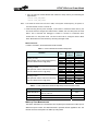
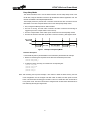
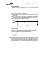
HT32F125x Low Power Mode HT32F125x Low Power Mode D/N:HA0284E Introduction Induction This application note is intended to help system designers to have a software and hardware implementation overview of the low-power modes of the HT32F125x series products. Users can learn how to use the HT32F125x products and low-power management so as to optimize the use of HT32F125x in low power applications. Related Documents HT32F125x Dataseet HT32F125x User Manual Power Consumption and Wakeup Time Measurement Introduction After reading this section, user can learn about the measurement of the HT32F125x low-power mode power consumptions and HT32F125x wake up timings. Power Measurement User can measure the power consumption of the HT32F125x with the firmware provided in the Zip file that comes together with this application note. This firmware is available in the Current Measurements folder. Power is measured in the following low-power modes: Sleep Mode Only the clock of CortexTM-M3 CPU core will be stopped during Sleep mode. Power consumption in this mode depends on the clock source and the active peripherals. To cover all the functionalities of this mode, measurements are made using different clock sources (HSI and HSE), clock frequencies (from 1MHz to 72 MHz), APB peripheral configurations (all peripheral clocks ON or all peripheral clocks OFF – including Flash and SRAM). Deep Sleep Mode 1 In Deep-Sleep mode 1, all clocks in VDD18 power domain are stopped, high speed oscillators (HSI, HSE) and PLL are turned off, and the power source of VDD18 is LDO (in low current mode). 1 HT32F125x Low Power Mode Deep Sleep Mode 2 The Deep-Sleep mode 2 is the same with Deep-Sleep mode 1 except the power source of VDD18 is DMOS. Power Down Mode Shut down VDD18 power domain and keep VDD33 and VBAK power domain. Note: 1. Please refer to the HT32F125x User Manual for more details on the different low-power modes. 2. For the Sleep and Deep Sleep modes, all unused I/O pins are configured as input floating. The Schmitt trigger input is disabled, leading to zero consumption for these I/O pins. How to Measure the Power Consumption For HT32F125x Development Board, the measurement of the power consumption is made by replacing jumper J25 by an ammeter and by powering the board from an external supply, or by using the USB cable. Firmware Description In the header file (main.h) several #define can be selected to parameterize the example. Uncomment the corresponding line in the main.h file to select the needed clock configuration for Sleep mode: #define HSE_PLL_ON #define HSE_PLL_ON_72MHz //#define HSE_PLL_ON_36MHz //#define HSE_PLL_ON_18MHz //#define HSE_PLL_OFF //#define HSE_PLL_OFF_8MHz //#define HSE_PLL_OFF_1MHz //#define //#define //#define //#define HSI_PLL_ON HSI_PLL_ON_72MHz HSI_PLL_ON_36MHz HSI_PLL_ON_18MHz //#define HSI_PLL_OFF //#define HSI_PLL_OFF_8MHz //#define HSI_PLL_OFF_1MHz Please uncommenting the respective line to select the needed low-power mode: #define SLEEP //#define DEEP_SLEEP_1 //#define DEEP_SLEEP_2 //#define POWER_DOWN Please uncommenting the respective line to select the needed peripheral clock selection (clock gating) : //#define SLEEP_ALLPERIPH_ENABLE #define SLEEP_ALLPERIPH_DISABLE User can select the needed FMC clock selection in sleep mode by uncommenting the respective line: //#define SLEEP_FMC_ENABLE #define SLEEP_FMC_DISABLE 2 HT32F125x Low Power Mode User can select the needed SRAM clock selection in sleep mode by uncommenting the respective line. //#define SLEEP_SRAM_ENABLE //#define SLEEP_SRAM_DISABLE Note: 1. No mater the clock source is HSI or HSE, if the system clock frequency is equal to or less than 8 MHz, the PLL is turned off. 2. After executing the low-power example, if user wants to reload the Flash memory, the boot mode must be changed from Main Flash to SRAM, and must also press the reset button. This is because the debugger is unable to connect to HT32F125x when HT32F125x is in low-power mode. The boot mode must be configured back to Main Flash. Measurement is then started by rebooting the target board. Measure Results In Table 1 and Table 2, the measurement results are listed: Table 1 Power measurement results in Sleep mode Condition fHCLK Running on HSE, AHB prescaler used to reduce the frequency, FMC and SRAM clocks off @ Sleep Running on HSE, AHB prescaler used to reduce the frequency, FMC and SRAM clocks on @ Sleep Running on HSI, AHB prescaler used to reduce the frequency, FMC and SRAM clocks off @ Sleep 72MHz 36MHz 18MHz 8MHz 1MHz 72MHz 36MHz 18MHz 8MHz 1MHz 72MHz 36MHz 18MHz 8MHz 1MHz All APB Peripherals Enabled 26.42mA 15.64mA 10.1mA 4.39mA 2.21mA 28.27mA 16.57mA 10.57mA 4.6mA 2.24mA 26.39mA 15.5mA 9.97mA 4.33mA 2.15mA All APB Peripherals Disabled 6.76mA 5.25mA 4.49mA 1.43mA 1.13mA 8.67mA 6.21mA 4.98mA 1.64mA 1.16mA 6.63mA 5.12mA 4.36mA 1.36mA 1.06mA Table 2 Power measurement results in Deep Sleep and Power Down modes Power Mode Condition VDD33/VBAT = 3.3V Deep Sleep Mode 1 VDD18 use LDO, LDO in low power mode, RTC on, use LSI 67uA Deep Sleep Mode 2 VDD18 use DMOS, LDO Off, RTC on, use LSI 11.5uA Power Down Mode VDD18 Off, RTC on, use LSI 4.5uA Wake-up Time Measurement This section describes how to measure the time required by the HT32F125x to wake up from different low-power modes. The related firmware is provided with this application note. The firmware is found in the Zip file in the Wake-up Timing folder. 3 HT32F125x Low Power Mode The wakeup time definition: Sleep and Deep Sleep modes: The wakeup time starts on the rising edge of RTCOUT(PB10) and ends after the execution of the first instruction after the WFE. For Power Down mode: After waking up from Power Down mode, program execution restarts as same as a Reset condition. The Power Down mode wakeup time is the time between the rising of RTCOUT(PB10) and the execution of the first instruction of the code. How to Measure the Wake-up Time Pin PA5 is set after waking up from the low-power modes, to measure the wakeup time, an oscilloscope should be connected across the PA5 and PB10 pins. The wakeup time is the time between the rising edge of PB10 (RTCOUT) and the rising edge of PA5. Firmware Description In the header file (main.h) several #define can be selected to parameterize the example. Please uncommenting the respective line to select the needed low-power mode. //#define //#define //#define //#define SLEEP DEEP_SLEEP_1 DEEP_SLEEP_2 POWER_DOWN Uncommenting the respective line to select the needed system clock source. /* Define the system clock */ #define HCLK_HSI //#define HCLK_HSI_PLL //#define HCLK_HSE //#define HCLK_HSE_PLL In the main file (main.c). Before entering a low-power mode, PA5 is configured as an output push-pull and reset to the low level. After wakeup from low-power mode: For the Sleep and Deep Sleep modes, a direct write to the GPIOA_SRR (Output Set Reset Control register) is performed to set PA5 to the high level For Power Down mode, pin PA5 should be set at the code startup (this part of the code is managed in the startup files. See below). To measure the wakeup time for the Power Down mode, please first configure and set the PA5 pin. To manage this, the following assembly code is added to the tools startup file: ;/* LDR LDR STR ;/* LDR LDR STR STR Enable peripheral clocks of AFIO and GPIOA */ R0, = 0x4008802C R1, = 0x00014000 R1,[R0] PA5 output high */ R0, = 0x4001A000 R1, = 0x0020 R1,[R0, #0x24] R1,[R0] Note: After executing the low-power example, if user wants to reload the Flash memory, the boot mode configuration must be changed from Main Flash to SRAM, and then press the reset button. This is because the debugger is unable to connect to HT32F125x when HT32F125x is in low-power mode. The boot mode must be configured back to Main Flash. Measurement is then started by rebooting the target board. 4 HT32F125x Low Power Mode Measurement Results The wake-up time measurements in the Sleep, Deep Sleep and Power Down modes are listed in Table 3. Table 3 Wake-up time measurement results Symbol Parameter Condition Typical Value tWUSLEEP Wake up from Sleep Mode 1.04us tWUDS1 Wake up from Deep Sleep Mode 1 17.4us tWUDS2 Wake up from Deep Sleep Mode 2 Wake up on HSI clock 17.4us tWUPD Wake up from Power Down Mode 118us tWUSLEEP Wake up from Sleep Mode 1.04us tWUDS1 Wake up from Deep Sleep Mode 1 tWUDS2 Wake up from Deep Sleep Mode 2 tWUSLEEP Wake up from Sleep Mode tWUDS1 Wake up from Deep Sleep Mode 1 tWUDS2 Wake up from Deep Sleep Mode 2 tWUSLEEP Wake up from Sleep Mode tWUDS1 Wake up from Deep Sleep Mode 1 tWUDS2 Wake up from Deep Sleep Mode 2 Wake up on HSE clock Wake up on PLL clock PLL uses HSI Wake up on PLL clock PLL uses HSE 5.04ms 5.04ms 0.2us 146us 146us 0.2us 5.16ms 5.16ms Conclusion From the different results user can see the trade-off between power consumption and wakeup time in the HT32F125x. The condition is: the lower the power consumption, the longer the wakeup time. By the way, as HSE and PLL require longer ready time, so when clock source is HSE or PLL, the Deep Sleep mode Wakeup time will be longer。To reduce the Wakeup time of Deep Sleep Mode, user can use the HSI first and then switch to other user preferred clock source(System Clock, HSE or PLL)。 User should find the best trade-off according to the user application constraints. Power Consumption Optimization Introduction As a matter of fact: microcontroller power consumption increases with the clock frequency. So, user has to find the best ratio between power consumption and overall system performance. In many applications, power consumption can be reduced by adjusting system/peripheral frequency to the required performance. If no specific system/peripheral activity is required, the low-power modes of the HT32F125x can be used. Using the Clock Configuration in Your Application This section describes how to use the clock configuration of the HT32F125x, using a firmware found in the Zip file delivered with this application note. This firmware is available in the Run_Mode folder. 5 HT32F125x Low Power Mode This program sends the time from RTC through the USART of HT32F125x. First, the user has to adjust the time using the HyperTerminal. Time is displayed on the HyperTerminal and refreshed every second. The RTC is configured to generate an interruption every second. When the interruption occurs, the RTC counter is captured; the time is calculated and sent through USART. Hardware Environment Use this example with HT32F125x Development board: please refer to the HT32F125x Development Board Use the USART cable found in the HT32F125x Development board package. A null-modem female/female RS232 cable must be connected between the DB9 connector and the PC serial port. The measurement of the power consumption is made by replacing jumper J25 by an ammeter. Firmware Description Configure HyperTerminal on the PC Word length = 8 bits One Stop bit No parity Baud rate = 115200 flow control: none Configure the firmware In the header file (main.h) several #define can be selected to parameterize the example. #define for peripheral selection (clock gating) //#define ALL_PERIPHERIALS_ENABLE //#define ONLY_USART_RTC_ENABLE #define for frequency selection //#define HCLK_72MHz //#define HCLK_8MHz #define for switching to Sleep mode while the application is waiting for the RTC interrupt //#define SLEEP_WFI_ON Note: After executing the low-power example, if user wants to reload the Flash memory, the boot mode configuration must be changed from Main Flash to SRAM, and then press the reset button. This is because the debugger is unable to connect to HT32F125x when HT32F125x is in low-power mode. The boot mode must be configured back to Main Flash. Measurement is then started by rebooting the target board. 6 HT32F125x Low Power Mode Measurement Results Table 4 Example measurements of Run Mode at 25 °C Peripheral Clock Frequency Sleep Typical Consumption ALL On 72MHz No 51.8mA Only RTC On 72MHz No 37.4mA Only RTC On 72MHz Yes 12.7mA Only RTC On 8MHz No 11.1mA Only RTC On 8MHz Yes 2.05mA Conclusion For reducing the power consumption, HT32F125x has to be initialized with an optimized configuration according to the user application. The user must focus on the application requirements and configure the HT32F125x accordingly. From this example, user can learn the possible HT32F125x clock configurations and to optimize the power consumption of an application. The configurations are described below: System and Peripheral Frequency If the application does not need to run at the maximum frequency, the user can reduce HCLK by using the PLL or the prescaler divisor. Clock Gating To optimize power consumption, user should disable the unused peripherals by the HT32F125x clock gating configurations. Sleep Mode Another way of reducing power consumption is to switch to the HT32F125x Sleep mode when the application is waiting for an event or an interrupt. Using the Deep Sleep and Power Down mode in battery-operated application Introduction Some applications powered by a standard battery are not running all the time. In this kind of applications, the microcontroller waits for an external event, and needs to reduce its power consumption during the not running phase. The software provided with this application note gives two examples (DeepSleepMode and PowerDownMode) of how to use the HT32F125x in battery-operated applications. In the examples the HT32F125x switches to low-power mode as soon as the application does not require processing. The two low-power modes are based on the Cortex-M3 core’s Deep Sleep feature and WFE instruction. 7 HT32F125x Low Power Mode Deep Sleep Mode This section describes how to use the WFE instruction and the Deep Sleep mode of the HT32F125x, using the firmware found in the Zip file delivered with this application note. The firmware is available in the DeepSleepMode folder. The example performs a periodic ADC conversion and stores the ADC conversion result in RAM buffer. It uses RTC Compare Match event to auto wakeup Deep Sleep modes. First, configure the Backup Domain, GPIO and ADC. The RTC is running, and each ADC conversion and ADC conversion result storage is triggered by the RTC compare match in the main loop. The RTC compare match event wakes up the HT32F125x from the Deep Sleep modes. The PA5 I/O shows the time taken by the ADC conversion and RTC_CMP register reload. Figure 1 Example of Deep Sleep Mode Firmware Description In the header file (main.h) several #define can be selected to parameterize the example. Please uncommenting the respective line to select the needed low-power mode: //#define DEEP_SLEEP_1 //#define DEEP_SLEEP_2 To select the timing of the loop, uncomment the corresponding line: //#define //#define //#define //#define //#define LOOP_50mS LOOP_500mS LOOP_1S LOOP_3S LOOP_5S Note: After executing the low-power example, if user wants to reload the Flash memory, the boot mode configuration must be changed from Main Flash to SRAM, and then press the reset button. This is because the debugger is unable to connect to HT32F125x when HT32F125x is in low-power mode. The boot mode must be configured back to Main Flash. Measurement is then started by rebooting the target board. 8 HT32F125x Low Power Mode Power Down Mode This section describes how to use the Power Down mode of the HT32F125x, using the firmware found in the Zip file delivered with this application note. The firmware is available in the PowerDownMode folder. The example performs a periodic ADC conversion and stores the ADC conversion result in RAM buffer. It uses RTC Compare Match event to auto wakeup Power Down mode. First, configure the Backup Domain, GPIO and ADC. The RTC is running and RTC Compare Match event wakeup the HT32F125x from Power Down mode. After each wakeup from Power Down mode, the HT32F125x restarts from the reset state and each ADC conversion is performed after the HT32F125x has been configured. The PA5 I/O shows the time taken by the program running. Figure 2 Example of Power Down Mode Firmware Description In the header file (main.h) several #define can be selected to parameterize the example. To select the timing of the loop, uncomment the corresponding line: //#define //#define //#define //#define //#define LOOP_50mS LOOP_500mS LOOP_1S LOOP_3S LOOP_5S Note: After executing the low-power example, if user wants to reload the Flash memory, the boot mode configuration must be changed from Main Flash to SRAM, and then press the reset button. This is because the debugger is unable to connect to HT32F125x when HT32F125x is in low-power mode. The boot mode must be configured back to Main Flash. Measurement is then started by rebooting the target board. 9 HT32F125x Low Power Mode How to Measure the Current Consumption For HT32F125x Development Board, the measurement of the power consumption is made by replacing jumper J25 by an ammeter and by powering the board from an external supply, or by using the USB cable. Measurement Results Table 5 shows the measurements. Table 5 Example measurements of Low-Power mode at 25°C Low Power Mode 50ms 500ms 1s 3s 5s Deep Sleep Mode 1 77.2uA 69.3uA 69.2uA 68.6uA 68.5uA Deep Sleep Mode 2 23.4uA 14.3uA 13.8uA 13.4uA 13.4uA Power Down Mode 363.2uA 46.2uA 26.4uA 10.7uA 8.8uA Conclusion Because the Cortex-M3 CPU core integrates the efficient Core-level instructions for low-power applications (Sleep mode and Deepsleep mode), together with the low-power features of the HT32F125x, user can optimize system power consumption according to the application requirement. Measurements show that the trade-off between wakeup time and power consumption must be taken into account. 10