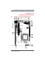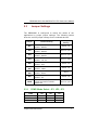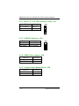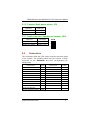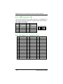
1
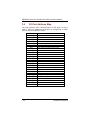
SBC826A0 All-in-One Half-Size PCI CPU CARD and Serial ATA User’s Manual Disclaimers The information in this manual has been carefully checked and is believed to be accurate. Axiomtek Co., Ltd. assumes no responsibility for any infringements of patents or other rights of third parties which may result from its use. Axiomtek assumes no responsibility for any inaccuracies that may be contained in this document. Axiomtek makes no commitment to update or to keep current the information contained in this manual. Axiomtek reserves the right to make improvements to this document and/or product at any time and without notice. No part of this document may be reproduced, stored in a retrieval system, or transmitted, in any form or by any means, electronic, mechanical, photocopying, recording, or otherwise, without the prior written permission of Axiomtek Co., Ltd. Copyright 2004 by Axiomtek Co., Ltd. All rights reserved. July 2004, Version A1 Printed in Taiwan ii ESD Precautions Integrated circuits on computer boards are sensitive to static electricity. To avoid damaging chips from electrostatic discharge, observe the following precautions: Do not remove boards or integrated circuits from their anti-static packaging until you are ready to install them. Before handling a board or integrated circuit, touch an unpainted portion of the system unit chassis for a few seconds. This helps to discharge any static electricity on your body. Wear a wrist-grounding strap, available from most electronic component stores, when handling boards and components. Trademarks Acknowledgments AXIOMTEK is a trademark of Axiomtek Co., Ltd. IBM is a registered trademark of International Business Machines Corporation. MS-DOS, and Windows 95/98/NT/2000 are trademarks of Microsoft Corporation. Phoenix-Award is a trademark of Phoenix-Award Software, Inc. IBM, PC/AT, PS/2, VGA are trademarks of International Business Machines Corporation. Intel and Celeron, Pentium III are trademarks of Intel Corporation. Other brand names and trademarks are the properties and registered brands of their respective owners. iii Table of Contents Chapter 1 Introduction............................................................1 1.1 Specifications ................................................................2 1.2 Utilities Supported.........................................................4 Chapter 2 Jumpers and Connectors......................................5 2.1 Board Layout and Fixing Holes....................................5 2.2 Connector and Jumper Locations ...............................6 2.3 Jumper Settings.............................................................7 2.3.1 COM2 Mode Select: JP1, JP2, JP3 ................................. 7 2.3.2 IGA2 TTL LCD VDD Selection (CN2): JP4 ................. 8 2.3.3 AT&ATX Selection: JP5 ................................................ 8 2.3.4 CMOS Clear Jumper: JP6 .............................................. 8 2.3.5 Compact flash Master/Slave: JP8.................................. 8 2.3.6 Compact flash power select: JP9 ................................... 9 2.3.7 Audio Line Out/Speaker Out Jumper: JP10.................. 9 2.4 Connectors.....................................................................9 2.4.1 USB Connector: CN1 ....................................................10 2.4.2 IGA2 24bit TTL Connector: CN2.................................10 2.4.3 SATA-150 Connectors: CN3, CN4................................12 2.4.4 DVI Output Connector: CN6 .......................................13 2.4.5 AUDIO Connector: CN7..............................................13 2.4.6 ATX Connector: CN8 ...................................................14 2.4.7 Front Panel Bezel Connector: CN9 ..............................14 2.4.8 IrDA Connector: CN10 .................................................15 2.4.9 Keyboard and Mouse Connectors ................................15 2.4.10 ACPI Connector ..........................................................16 2.4.11 FAN Connector: FAN1................................................16 2.4.12 Floopy Disk Connector: FDD1 ...................................17 2.4.13 COM PORT Connectors: COM1~2............................17 2.4.14 PRINT PORT Connector: LPT1 ................................18 2.4.15 Compact Flash Slot: CF1.............................................19 iv Chapter 3 Haredware Description......................................21 3.1 3.2 3.3 3.4 3.5 Microprocessors..........................................................21 BIOS ...........................................................................21 System Memory ...........................................................21 I/O Port Address Map ..................................................22 Interrupt Controller......................................................23 Chapter 4 Award BIOS Utility ............................................25 4.1 BIOS Introduction ........................................................25 4.2 BIOS Setup ...................................................................25 4.2.1 Standard CMOS Setup ..................................................27 4.2.2 Advanced BIOS Features .............................................30 4.2.3 Advanced Chipset Features..........................................35 4.2.4 Integrated Peripherals ..................................................38 4.2.5 Power Management Setup............................................44 4.2.6 PNP/PCI Configuration ..............................................47 4.2.7 PC Health Status ..........................................................49 4.2.8 Frequency/Voltage Control .........................................50 4.2.9 Load Fail-Safe Defaults ................................................51 4.2.10 Set Supervisor/User Password....................................52 4.2.11 Save & Exit Setup........................................................53 4.2.12 Exit Without Saving ....................................................54 Appendix A Serial ATA Setup Information.....................55 Appendix B Watchdog Timer ..............................................57 v This page does not contain any information. vi SBC826A0 All-in-One Half-Size PCI CPU Card User’s Manual Chapter 1 Introduction The SBC826A0 is an industrial grade CPU card. It provides reliable high performance and function-rich capability. The SBC826A0 with Socket 370 can adapt a wide variety of Celeron and Pentium III microprocessors. The CPU incorporates the VIA CLE266 north bridge and the VT8237 south bridge. The CLE266 provides superior performance between the CPU, SDRAM, V-Link bus and internal AGP-8x VGA controller. The PCI Bus Controller of VT8237 ensures the compatibility with PCI bus passive backplanes. The SBC826A0 packs the unique features of Graphics (CRT or DVI) +LCD, Serial ATA, Ethernet (Gigabit & Fast), USB2.0 and etc. Designed for the professional embedded developers, the Socket370 all-in-one SBC826A0 Half-Size CPU card is virtually the ultimate one-step solution to various applications. Introduction 1 SBC826A0 All-in-One Half-Size PCI CPU CardUser’s Manual 1.1 Specifications CPU: Socket 370 for Intel Celeron, Pentium III, Tualatin Chipset: Bus Clock: VIA CLE266 and VT8237 66,100,133MHz L2 Cache: Integrated in CPU BIOS: 4Mbit PnP Flash BIOS System Memory: 1 x 184-pin DIMM sockets Maximum of 1GB DDR266 RAM IDE Interface: IDE1 x 40-pin CF with IDE2 channel PIO Mode 0-4, DMA Mode 0-2 and Ultra DMA/33/66/100/133 2 channels of SATA-150 with RAID 0 or 1 supported BIOS programmable for 4 IE channels (2*PATA-133 & 2*SATA-150) as primary/secondary/third/forth IDE Onboard Multi-I/O: One FDD supporting up to two devices One SPP/EPP/ECP parallel port (box header) Two serial ports: 1x RS-232, 1x RS-232/422/485 selectable via jumper One IrDA for wireless communication One Keyboard Interface One Mouse Interface One Mini-DIN PS/2 connector for Keyboard and Mouse VGA Controller: AGP interface controller integrated in VIA CLE266 Supports DVI/CRT and 24-bit LCD Extended Screen Resolutions up to 1600x1200 Supports DualView feature as DVI + TTL LCD LCD Backlight control supported 2 Introduction SBC826A0 All-in-One Half-Size PCI CPU Card User’s Manual Ethernet: Dual Realtek 8100C PCI Bus 10/100M Base-T or one Realtek 8100C PCI Bus 10/100M Base-T and one Realtek 8110s PCI Bus 10/100/1000M Base-T Wake On LAN (via ATX power supply) Onboard Dual RJ-45 connectors USB Interface: USB ports; USB Spec. Rev. 2.0 compliant Audio AC’97 2.2 S/PDIF extension compliant codec 18-bit stereo full duplex SD codec 3D stereo expansion for simulated surround 18-bit independent rate stereo ADC/DAC 4 stereo, 2 mono analog line-level inputs Low Power consumption mode Exceeds Microsoft® WHQL logo requirements Compact Flash TYPE II Supports CompactFlash memory modules IBM MicroDrive supported Power Management: ACPI (Advanced Configuration and Power Interface) Watchdog Timer: Watch Dog Timer Time-out value. of 0~255 second/minutes Operating Temperature: 0 o C~60 o C (32 o F~140 o F) Operating Humidity: 5%~95%; non-condensing Dimensions: 121.92 mm x 185 mm NOTE: Specifications are subject to change without notice. Introduction 3 SBC826A0 All-in-One Half-Size PCI CPU CardUser’s Manual 1.2 Utilities Supported VIA Chipset Driver Ethernet Utility and Drivers VGA Drivers 4 Introduction SBC826A0 All-in-One Half-Size PCI CPU Card User’s Manual Chapter 2 Jumpers and Connectors 2.1 Board Layout and Fixing Holes Jumpers and Connectors 5 SBC826A0 All-in-One Half-Size PCI CPU CardUser’s Manual 2.2 6 Connector and Jumper Locations Jumpers and Connectors SBC826A0 All-in-One Half-Size PCI CPU Card User’s Manual 2.3 Jumper Settings The SBC826A0 is configured to match the needs of the application by proper jumper settings. The following tables show the correct jumper settings for the onboard devices. Jumper Jumper Setting Default Setting JP1 COM2 RS232/422/485 Default: RS232 Short 1-2 JP2 COM2 RS232/422/485 Default: RS232 Short 3-5,4-6 JP3 COM2 RS232/422/485 Default: RS232 Short 3-5,4-6 JP4 JP5 IGA2 TTL LCD VDD Selection Default: TTL 5V AT&ATX Selection Short 1-2(5V) Short 2-3 Default: ATX JP6 Clear CMOS Selection Default: VBAT JP8 CF Master/Slave Default: Slave JP9 Compact flash power select Default: 5V Short 1-2 JP10 Audio Line Out/Speaker Out Jumper Selection Default: Speak Out Short 3-5,4-6 2.3.1 Short 1-2 Short COM2 Mode Select: JP1, JP2, JP3 COM2 RS-232 (default) RS-422 RS-485 JP3 JP2 JP1 3-5, 4-6 1-3, 2-4 1-3, 2-4 3-5, 4-6 1-3, 2-4 1-3, 2-4 1-2 3-4 5-6, 7-8 Jumpers and Connectors 7 SBC826A0 All-in-One Half-Size PCI CPU CardUser’s Manual 2.3.2 IGA2 TTL LCD VDD Selection (CN2): JP4 VDDM 5V (TTL default) 3.3V Settings Short 1-2 Short 2-3 JP4 1 2 3 2.3.3 AT&ATX Selection: JP5 Select AT POWER ATX POWER Settings Short 1-2 Short 2-3(Default) JP5 1 2 3 2.3.4 CMOS Clear Jumper: JP6 Options Normal (default) Clear CMOS Settings Short 1-2 Short 2-3 2.3.5 Compact flash Master/Slave: JP8 Options Slave(default) Master 8 Settings Open Short Jumpers and Connectors SBC826A0 All-in-One Half-Size PCI CPU Card User’s Manual 2.3.6 Compact flash power select: JP9 Options 5V(default) 3.3V Settings Short 1-2 Short 2-3 2.3.7 Audio Line-out / Speaker-out Jumper: JP10 Options Line Out Speaker Out (default) 2.4 JP10 Settings Short 1-3, 2-4 Short 3-5, 4-6 1 2 3 4 5 6 Connectors The connectors allow the CPU card to connect with other parts of the system. The following table lists the function of each connector on the SBC826A0 and their corresponding pin assignments. Connectors Label Connectors Label USB Connector IGA2 24bit TTL Connector S-ATA 1 Connector S-ATA 2 Connector DVI Connector AUDIO Connector Power Connector Front Panel Bezel Connector IRDA Connector Keyboard and Mouse Connectors (Mini DIN) Ext PS/2 Keyboard Connector CN1 CN2 CN3 CN4 CN6 CN7 CN8 CN9 CN10 CN11 Ext PS/2 Mouse Connector ACPI Connector CPU FAN Connector Floppy Disk Connector COM PORT Connector PRINT PORT Connector Compact Flash Slot IDE Connector LAN RJ45 Connector LAN RJ45 Connector CN13 CN14 FAN1 FDD1 COM1~2 LPT1 CF1 IDE1 LAN1 LAN2 Jumpers and Connectors CN12 9 SBC826A0 All-in-One Half-Size PCI CPU CardUser’s Manual 2.4.1 USB Connector: CN1 The Universal Serial Bus (USB) connector on SBC826A0 is used when installing peripherals supporting the USB interface. CN1: USB 1 Connector Pin 1 3 5 7 9 Description VCC USB1+ USB1GND GND Pin 2 4 6 8 10 Description VCC USB2+ USB2GND GND 2 4 6 8 10 1 3 5 7 9 2.4.2 IGA2 24bit TTL Connector: CN2 Pin 1 4 7 10 13 16 19 22 25 28 31 34 37 40 43 10 Signal -12V GND ENAVEE P1 P4 P7 P10 P13 P16 P19 P22 GND M ENABKL VCCM Pin 2 5 8 11 14 17 20 23 26 29 32 35 38 41 44 Signal +12VM VCCM GND P2 P5 P8 P11 P14 P17 P20 P23 SHFCLK LP GND VCCM Pin 3 6 9 12 15 18 21 24 27 30 33 36 39 42 Signal GND VCCM P0 P3 P6 P9 P12 P15 P18 P21 GND FLM GND -SHFCLK Jumpers and Connectors SBC826A0 All-in-One Half-Size PCI CPU Card User’s Manual Flat Panel Interface Pins for Color TFT LCD Pin 18-bit 24-bit LP FLM SHFCLK M ENAVDD ENABLK P23 P22 P21 P20 P19 P18 P17 P16 P15 P14 P13 P12 P11 P10 P9 P8 P7 P6 P5 P4 P3 P2 P1 P0 HSYNC VSYNC CK DE ENAVDD ENABLK R5 R4 R3 R2 R1 R0 HSYNC VSYNC CK DE ENAVDD ENABLK R7 R6 R5 R4 R3 R2 R1 R0 G7 G6 G5 G4 G3 G2 G1 G0 B7 B6 B5 B4 B3 B2 B1 B0 Jumpers and Connectors G5 G4 G3 G2 G1 G0 B5 B4 B3 B2 B1 B0 11 SBC826A0 All-in-One Half-Size PCI CPU CardUser’s Manual Flat Panel Connector Pin Description Name Description P0~P35 ENABKL SHFCLK M LP Flat panel data output Activity Indicator and Enable Backlight outputs Shift clock. Pixel clock for flat panel data M signal for panel AC drive control Latch pulse. Flat panel equivalent of HSYNC First line marker. Flat panel equivalent of VSYNC +12V power controlled by chipset Power sequencing controls for panel LCD bias volt 3.3V or 5V selected by JP2 FLM +12VM ENAVEE VCCM 2.4.3 SATA-150 Connectors: CN3, CN4 Dual Channel Serial ATA / RAID Controller Complies with Serial ATA Specification Revision 1.0 Dual Channel master mode PCI On-chip two-channel Serial ATA (S-ATA) PHY for support of up to two S-ATA devices directly Supports optional external S-ATA PHY on P-ATA secondary port for support of two additional S-ATA devices Primary P-ATA port can support two P-ATA devices (master and slave) along with two S-ATA devices on the PATA secondary port (with external S-ATA PHY) plus two more SATA devices on the direct S-ATA interface S-ATA devices can be configured in multiple RAID configurations - supports RAID Level 0, RAID Level 1, RAID Level 0+1 and JBOD S-ATA drive transfer rate is capable of up to 150 MB/s per channel (serial speed of 1.5 Gbit/s) External Crystal input for Serial ATA port operation 12 Jumpers and Connectors SBC826A0 All-in-One Half-Size PCI CPU Card User’s Manual 2.4.4 DVI Output Connector: CN6 1 TX2- 2 TX2+ 3 Ground 4 NC 5 NC 6 SPCLK 7 SPD DATA 8 CRT-VSYNC 9 TX1- 10 11 Ground 12 NC 13 TX1+ NC 14 VGAVCC 15 Ground 16 FPDETECT 17 TX0- 18 TX0+ 19 Ground 20 NC 21 NC 22 Ground 23 TXC+ 24 TXC- C1 CRT-RED C2 CRT-GREEN C3 CRT-BLUE C4 CRT-HSYNC C5 VGAGND C6 NC 2.4.5 AUDIO Connector: CN7 CN7: Audio Connector Pin 1 3 5 7 9 Signal MIC-IN Line In L Line In R Audio Out L Audio Out R Pin 2 4 6 8 10 Jumpers and Connectors Signal GND GND GND GND GND 2 4 6 8 10 1 3 5 7 9 13 SBC826A0 All-in-One Half-Size PCI CPU CardUser’s Manual 2.4.6 ATX Connector: CN8 Pin Description 1 +5V GND +12V SB5V GND +5V 2 3 4 5 6 6 5 4 3 2 1 2.4.7 Front Panel Bezel Connector: CN9 CN9 Power LED This 3-pin connector, designated at Pins 1,3 and 5, connects the system power LED indicator to its respective switch on the case. Pin 1 is +; pin 3 and 5 is assigned as -. The Power LED lights up when the system is powered ON. External Speaker and Internal Buzzer Connector Pins 2, 4, 6, and 8 of CN9 connect to the case-mounted speaker unit or internal buzzer. Short pins 4-6 when connecting the CPU card to an internal buzzer. When connecting an external speaker, set these jumpers to Open and install the speaker cable on pin 8 (+) and pin 2 (-). System Reset Switch Pins 9 & 11 of CN9 connect to the case-mounted reset switch and allow rebooting of your computer instead of turning OFF the power switch. This is a preferred method of rebooting in order to prolong the life of the system’s power supply. 14 Jumpers and Connectors SBC826A0 All-in-One Half-Size PCI CPU Card User’s Manual HDD Activity LED This connector extends to the hard drive activity LED on the control panel. This LED will flash when the HDD is being accessed. Pins 10 & 12 of CN9 connect the hard disk drive and the front panel HDD LED. Pins 10 is -, and pin 12 is assigned as +. 2.4.8 IrDA Connector: CN10 CN10 is a 5-pin Pitch2.54mm IrDA connector for wireless communication. CN10 2.4.9 +5V 1 N.C. 2 IRRX 3 GND 4 IRTX 5 Keyboard and Mouse Connectors The SBC826A0 provides a keyboard (CN12) and a mouse (CN13) interface with a 5-pin connector. CN11 is a DIN connector for PS/2 keyboard/Mouse connection. CN12/CN13 Clock 1 Data 2 No Connection 3 GND 4 Power 5 Mouse Clock Keyboard Clock 6 VCC Mouse Data 5 4 3 2 1 GND Keyboard Data CN11 Jumpers and Connectors 15 SBC826A0 All-in-One Half-Size PCI CPU CardUser’s Manual 2.4.10 ACPI Connector Advanced Configuration and Power Interface (ACPI) defines a flexible and extensible interface that allows system designers to select appropriate cost/feature trade-offs for power management. The interface enables and supports reliable power management through improved hardware and operating system coordination. The specification enables new power management technology to evolve independently in operating systems and hardware while ensuring that they continue to work together. CN14 on the SBC826A0 is a 6-pin header connector that provides ACPI interface. CN14 1 4 5 6 E G P G X N W N T D _ D B S N M I 2 3 P W _ O N S B 5 V 2.4.11 FAN Connector: FAN1 Pin 1 2 3 16 Description Sensor +12V GND 3 2 1 Jumpers and Connectors SBC826A0 All-in-One Half-Size PCI CPU Card User’s Manual 2.4.12 Floppy Disk Connector: FDD1 The SBC826A0 provides a 26-pin connector which is the general output for a single floppy drive. The floppy drive could be any one of the following types: 3.5" 720KB or 1.44MB/2.88MB. FDD1: FDD Connector Pin Assignment Pin 1 4 7 10 13 16 19 22 25 28 31 34 Description GND No connector GND Motor enable A# GND Motor enable B# GND Write data# GND Write protect# GND Disk change# Pin Description Pin 2 Reduce write current GND Index# GND Drive select A# GND STEP# GND Track 0 # GND Side 1 select# 3 5 8 11 14 17 20 23 26 29 32 6 9 12 15 18 21 24 27 30 33 Description GND No connector GND Drive select B# GND Direction# GND Write gate# GND Read data# GND 2.4.13 COM PORT Connectors: COM1~2 SBC826A0 uses two 10-pin connectors for COM1 and COM2. Interrupt Requests on COM1 and COM2 which are selected via IRQ4 and IRQ3 respectively. Additionally, both ports can be enabled or disabled via BIOS setting. Pin Description Pin Description 1 3 5 7 9 Data Carrier Detect (DCD) Receive Data (RXD) Transmit Data (TXD) Data Terminal Ready (DTR) Ground (GND) 2 4 6 8 10 Data Set Ready (DSR) Request to Send (RTS) Clear to Send (CTS) Ring Indicator (RI) NC Jumpers and Connectors 2 1 3 4 5 6 7 9 8 10 17 SBC826A0 All-in-One Half-Size PCI CPU CardUser’s Manual The RS-422/485 pin assignments for COM2 are listed below. Pin # 1 2 3 4 5 6 7 8 9 10 Signal Name R2-422 TXNo connector TX+ No connector RX+ No connector RXNo connector GND No connector RS-485 DATANo connector DATA+ No connector No connector No connector No connector No connector GND No connector 2.4.14 PRINT PORT Connector: LPT1 LPT1: Parallel Port Connector Pin Assignment Pin 1 3 5 7 9 11 13 15 17 19 21 23 25 18 Description Strobe# Data 0 Data 1 Data 2 Data 3 Data 4 Data 5 Data 6 Data 7 Acknowledge# Busy Paper Empty# Printer Select Pin 2 4 6 8 10 12 14 16 18 20 22 24 26 Description Auto Form Feed# Error# Initialize# Printer Select In# GND GND GND GND GND GND GND GND NC 1 2 3 4 5 6 7 9 8 10 11 13 12 15 17 19 14 16 18 20 21 22 23 25 24 26 Jumpers and Connectors SBC826A0 All-in-One Half-Size PCI CPU Card User’s Manual 2.4.15 Compact Flash Slot: CF1 The SBC826A0 Series is equipped with a CompactFlash slot on the solder side and it supports the IDE interface CompactFlash disk card. The socket itself is especially designed to prevent any incorrect installation of the CompactFlash disk card. When installing or removing the CompactFlash disk card, please make sure that the system power is off. Jumpers and Connectors 19 SBC826A0 All-in-One Half-Size PCI CPU CardUser’s Manual This page does not contain any information. 20 Jumpers and Connectors SBC826A0 All-in-One Half-Size PCI CPU Card User’s Manual Chapter 3 Hardware Description 3.1 Microprocessors The SBC826A0 supports Intel Celeron and Pentium III CPUs. Systems based on these CPUs can be operated under Windows XP/NT/2000, Windows 98, DOS and Linux environments. The system performance depends on the microprocessor installed onboard. 3.2 BIOS System BIOS used on the SBC826A0 is Phoenix-Award Plug and Play BIOS. The SBC826A0 contains a single 4Mbit Flash. 3.3 System Memory The SBC826A0 industrial CPU board supports one 184-pin DDR DIMM (Dual In-Line Memory Module) socket for a maximum memory of 1GB buffer DDR266 SDRAMs. The memory module can come in sizes of 64MB, 128MB, 256MB, 512MB and 1GB. Hardware Description 21 SBC826A0 All-in-One Half-Size PCI CPU CardUser’s Manual 3.4 I/O Port Address Map The Intel Pentium CPU communicates via I/O ports. It has a total of 1KB port addresses available for assignment to other devices via I/O expansion cards. Address 000-01F 020-03F 060-06F 070-07F 080-09F 0C0-0DF 0F0 0F1 0F8-0FF 1F0-1F8 200-207 250-25F 278-27F 300-31F 360-36F 378-37F 380-38F 3A0-3AF 3B0-3BF 3C0-3CF 3D0-3DF 3F0-3F7 3F8-3FF 3E8-3EF 2F8-2FF 2E8-2EF 3F0-3FF 22 Devices DMA controller #1 Interrupt controller #1 Keyboard controller Real time clock, NMI DMA page register DMA controller #2 Clear math coprocessor busy signal Reset math coprocessor Math processor Fixed disk controller Game port Reserved Reserved Reserved Reserved Parallel port #1 Reserved Reserved MDA video card (including LPT1) VGA card CGA card Floppy disk controller Serial port #1 (COM1) Reserved Serial port #2 (COM2) Reserved Winbond I/O #1 Hardware Description SBC826A0 All-in-One Half-Size PCI CPU Card User’s Manual 3.5 Interrupt Controller NMI IRQ0 IRQ1 IRQ2 IRQ3 IRQ4 IRQ5 IRQ6 IRQ7 IRQ8 IRQ9 IRQ10 IRQ11 IRQ12 IRQ13 IRQ14 IRQ15 Hardware Description Parity check error System timer output Keyboard Interrupt rerouting from IRQ8 through IRQ15 Serial port #2 Serial port #1 Audio Floppy disk controller Parallel port #1 Real time clock Free Ethernet Ethernet PS/2 Mouse Math coprocessor Primary IDE channel Secondary IDE Channel 23 SBC826A0 All-in-One Half-Size PCI CPU CardUser’s Manual This page does not contain any information. 24 Hardware Description SBC826A0 All-in-One Half-Size PCI CPU Card User’s Manual Chapter 4 Award BIOS Utility Chapter 4 describes the different settings available in the Award BIOS that comes with the SBC826A0. Also contained here are instructions on how to set up the BIOS configuration. 4.1 BIOS Introduction The Award BIOS (Basic Input/Output System) installed in the system ROM supports Intel processors in a standard IBM-AT compatible I/O system. The BIOS provides critical low-level support for standard devices such as disk drives, serial and parallel ports. It also adds virus and password protection as well as special support for detailed fine-tuning of the chipset controlling the entire system. 4.2 BIOS Setup The Award BIOS provides a Setup utility program for specifying the system configurations and settings. The BIOS ROM of the system stores the Setup utility. When the computer is turned ON, the Award BIOS is immediately activated. The following message will appear on the screen: Press <DEL> to Enter Setup Then, press the <Del> key immediately to enter the Setup utility. The delay of pressing the <Del> key will cause POST (Power-on Self Test) to continue with the test routines, thus preventing invoking the Setup. In this case, the system has to be restarted for entering the BIO setup by pressing the ”Reset” button or simultaneously pressing the <Ctrl>, <Alt> and <Delete> keys. Besides, turning the system OFF first and then ON again can also restart the system. Award BIOS Utility 25 SBC826A0 All-in-One Half-Size PCI CPU CardUser’s Manual When entering the Setup utility, the Main Menu screen will appear on the screen. Various setup functions and exit choices can be selected from this menu. In general, the arrow keys are used to highlight items, <Enter> to select, the <PgUp> and <PgDn> keys to change entries, <F1> for help and <Esc> to quit. CMOS Setup Utility-Copyright © 1984-2001 Award Software Standard CMOS Features Frequency/Voltage Control Advanced BIOS Features Load Optimized Defaults Advanced Chipset Features Set User Password Integrated Peripherals Save & Exit Setup Power Management Setup Exit Without Saving PnP/PCI Configurations PC Health Status Esc : Quit F9 : Menu in BIOS F10 : Save & Exit Setup F6 : SAVE CMOS TO BIOS : Select Item F7 : LOAD CMOS FROM BIOS Time, Date, Hard Disk Type… The section below the setup items in the Main Menu displays the control keys for this menu. Another section located at the bottom of the Main Menu, just below the control keys section, displays information on the currently highlighted item in the list. NOTE: If the computer cannot boot after making and saving system changes with Setup, the Award BIOS, via its builtin override feature, resets your system to the CMOS default settings. Avoid making any changes to the chipset defaults are strongly recommended. These defaults have been carefully chosen by both Award and the system manufacturer to provide the absolute maximum performance and reliability. 26 Award BIOS Utility SBC826A0 All-in-One Half-Size PCI CPU Card User’s Manual 4.2.1 Standard CMOS Setup “Standard CMOS Setup” is used to record some basic hardware configurations in the computer system and set the system clock and error handling. If the motherboard is already installed in a working system, there is no need to enter this option. However, the Standard CMOS option has to be setup in any of the following situations: the system hardware configurations are changed, the onboard battery fails, and the configuration stored in the CMOS memory is lost or damaged. Phoenix – Award BIOS CMOS Setup Utility Standard CMOS Features Date (mm:dd:yy) Wed, Jul 20 2004 Item Help Time (hh:mm:ss) 13 : 9 : 11 Menu Level IDE Primary Master None IDE Primary Slave None Change the IDE Secondary Master None Day, month, IDE Secondary Slave None Year and Century Drive A 1.44M, 3.5 in. Drive B None Video Halt on EGA/VGA All, But keyboard Base Memory Extended Memory Total Memory 640K 494960k 491520k : Move Enter: Select +/-/PU/PD: Value F10: Save ESC: Exit F1: General Help F5: Previous Values F6: Fail-Safe Defaults F7: Optimized Defaults At the bottom of the menu are the control keys for the use of this menu. The <F1> key can be pressed in each item field to display the relevant information for help. The memory display at the lower right-hand side of the menu is read-only. It will adjust automatically according to the memory changed. The following pages describe each item of this menu. Award BIOS Utility 27 SBC826A0 All-in-One Half-Size PCI CPU CardUser’s Manual Date The date format is <day>, <date> <month> <year>. Press <F3> to show the calendar. day The day of week, from Sun to Sat, determined by the BIOS, is read only date The date, from 1 to 31 (or the maximum allowed in the month), can key in the numerical / function key month The month, Jan through Dec. year The year, depends on the year of BIOS Time The time format is <hour> <minute> <second> accepting either functional key or numerical key. The time is calculated based on the 24-hour military-time clock. For example, 1 p.m. is 13:00:00. IDE Primary Master/Primary Slave/Secondary Master/Secondary Slave This category identifies the type of the channel that is installed in the computer. There are 45 predefined types and 2 user definable types for Enhanced IDE BIOS. Type 1 to Type 45 are predefined. Type User is user-definable. Press <PgUp>/<+> or <PgDn>/<−> to select a numbered hard disk type or type the number and press <Enter>. Note that the specifications of the drive in the system must match with the drive table. The hard disk will not work properly if the improper information within this category is entered. If the disk drive type does not match or is not listed, the Type User is used to define the drive type manually. If the Type User is selected, related information has to be entered. Enter the information directly from the keyboard and press <Enter>. This information should be provided in the documentation from the hard disk vendor or the system manufacturer. If the controller of HDD interface is ESDI, select “Type 1”. If the controller of HDD interface is SCSI, select “None”. If the controller of HDD interface is CD-ROM, select “None”. 28 Award BIOS Utility SBC826A0 All-in-One Half-Size PCI CPU Card User’s Manual CYLS. number of cylinders LANDZONE landing zone HEADS number of heads SECTORS number of sectors PRECOMP write precom MODE HDD access mode If there is no hard disk drive installed, select NONE and press <Enter>. Drive A type/Drive B type The category identifies the types of floppy disk drive A or drive B installed in the computer. None No floppy drive installed 360K, 5.25 in 5.25 inch PC-type standard drive; 360Kb capacity 1.2M, 5.25 in 5.25 inch AT-type high-density drive; 1.2MB capacity 720K, 3.5 in 3.5 inch double-sided drive; 720Kb capacity 1.44M, 3.5 in 3.5 inch double-sided drive; 1.44MB capacity 2.88M, 3.5 in 3.5 inch double-sided drive; 2.88MB capacity Halt On This field determines whether the system will halt if an error is detected during power up. No errors The system boot will halt on any error detected. (default) All errors Whenever the BIOS detects a nonfatal error, the system will stop and you will be prompted. All, But Keyboard The system boot will not stop for a keyboard error; it will stop for all other errors. All, But Diskette The system boot will not stop for a disk error; it will stop for all other errors. All, But Disk/Key The system boot will not stop for a keyboard or disk error; it will stop for all other errors. Award BIOS Utility 29 SBC826A0 All-in-One Half-Size PCI CPU CardUser’s Manual 4.2.2 Advanced BIOS Features This section is used to configure and improve the system and set up some system features according to the user’s preference. Phoenix – Award BIOS CMOS Setup Utility Advanced BIOS Features Hard Disk Boot Priority Virus Warning CPU Internal Cache CPU L2 Cache ECC Checking Quick Power On Self Test First Boot Device Second Boot Device Third Boot Device Boot Other Device Onboard LAN boot Rom Swap Floppy Drive Boot Up Floppy Seek Boot Up NumLock Status Gate A20 Option Typematic Rate Setting Typematic Rate (Chars/Sec) Typematic Delay (Msec) Security Option MPS Version Control For OS OS Select For DRAM > 64MB Video BIOS Shadow Small Logo(EPA) Show Display Board ID Message Press Enter Disabled Enabled Enabled Enabled Floppy HDD-0 LS120 Enabled Disable Disabled Enabled On Fast Disabled 6 250 Setup 1.4 Non-OS2 Enabled Disabled Disabled Item Help Menu Level Allows you to choose the VIRUS warning feature for IDE Hard disk boot sector protection. If this function is enable and someone attempts to write data into this area, BIOS will show a warning message on screen and alarm beep : Move Enter: Select +/-/PU/PD: Value F10: Save ESC: Exit F1: General Help F5: Previous Values F6: Fail-Safe Defaults F7: Optimized Defaults 30 Award BIOS Utility SBC826A0 All-in-One Half-Size PCI CPU Card User’s Manual Virus Warning This item protects the boot sector and partition table of the hard disk against accidental modifications. If an attempt is made, the BIOS will halt the system and display a warning message. If this occurs, the user can either continue the operation or run an antivirus program to locate and remove the problem. NOTE: Many disk diagnostic programs, which attempt to access the boot sector table, can cause the virus warning. Thus, disable the Virus Warning feature while running any of these programs. CPU Internal Cache / External Cache Cache memory is additional memory that is much faster than conventional DRAM (system memory). CPUs from 486-type and up contain internal cache memory, and most, but not all, modern PCs have additional (external) cache memory. When the CPU requests data, the system transfers the requested data from the main DRAM into cache memory, for even faster access by the CPU. These items are used to enable (speed up memory access) or disable the cache function. By default, these are Enabled. CPU L2 Cache ECC Checking When enabled, this allows ECC checking of the CPU’s L2 cache. By default, this field is Enabled. Processor Number Feature When a Pentium III CPU is installed, the system automatically detects it and displays this item. Quick Power On Self Test This option speeds up Power-on Self Test (POST) after turning on the system power. If it is set as Enabled, BIOS will shorten or skip some check items during POST. The default setting is “Enabled”. Enabled Disabled Enable Quick POST Normal POST First/Second/Third Boot Device These items allow the selection of the 1st, 2nd, and 3rd devices that the system will search for during its boot-up sequence. The wide range of selection includes Floppy, LS120, ZIP100, HDD0~3, SCSI, CDROM, USB Floppy, USB CDROM, USB, HDD and LAN. Award BIOS Utility 31 SBC826A0 All-in-One Half-Size PCI CPU CardUser’s Manual Boot Other Device This item allows the user to enable/disable the boot device not listed on the First/Second/Third boot devices option above. The default setting is Enabled. Onboard LAN boot rom Choice Enable when you need boot on LAN Function, Like PXE ,RPL. Swap Floppy Drive This allows you to determine whether to enable Swap Floppy Drive or not. When enabled, the BIOS swaps floppy drive assignments so that Drive A becomes Drive B, and Drive B becomes Drive A. By default, this field is set to “Disabled”. Boot Up Floppy Seek During POST, BIOS will determine the floppy disk drive type, 40 or 80 tracks. 360Kb type is 40 tracks while 720Kb, 1.2MB and 1.44MB are all 80 tracks. The default value is “Enabled”. Enabled BIOS searches for floppy disk drive to determine if it is 40 or 80 tracks. Note that BIOS can not tell from 720K, 1.2M or 1.44M drive type as they are all 80 tracks. Disabled BIOS will not search for the type of floppy disk drive by track number. There will be no warning message displayed if the drive installed is 360K. Boot Up NumLock Status This option enables and disables the numberlock function of the keypad. The default value is “On”. On Keypad functions confine with numbers Off Keypad functions convert to special functions (i.e., left/right arrow keys) Gate A20 Option The default value is “Fast”. 32 Normal The A20 signal is controlled by keyboard controller or chipset hardware. Fast Default: Fast. The A20 signal is controlled by Port 92 or chipset specific method. Award BIOS Utility SBC826A0 All-in-One Half-Size PCI CPU Card User’s Manual Typematic Rate Setting This determines the typematic rate of the keyboard. The default value is “Disabled”. Enabled Enable typematic programming rate and typematic delay Disabled Disable typematic rate and typematic delay programming. The system BIOS will use default value of these 2 items and the default is controlled by keyboard. Typematic Rate (Chars/Sec) This option refers to the number of characters the keyboard can type per second. The default value is “6”. 6 8 10 12 15 20 24 30 6 characters per second 8 characters per second 10 characters per second 12 characters per second 15 characters per second 20 characters per second 24 characters per second 30 characters per second Typematic Delay (Msec) This option sets the display time interval from the first to the second character when holding a key. The default value is “250”. 250 500 750 1000 Award BIOS Utility 250 msec 500 msec 750 msec 1000 msec 33 SBC826A0 All-in-One Half-Size PCI CPU CardUser’s Manual Security Option This item limits the access to the system and Setup, or just to Setup. The default value is “Setup”. System Setup NOTE: The system will not boot and access to Setup will be denied if the incorrect password is entered at the prompt. The system will boot, but access to Setup will be denied if the correct password is not entered at the prompt. To disable security, select PASSWORD SETTING at Main Menu and then password is asked to enter. Do not type anything, just press <Enter> and it will disable security. Once the security is disabled, the system will boot and you can enter Setup freely. OS Select for DRAM > 64MB This segment is specifically created for OS/2 when DRAM is larger than 64MB. If the operating system is OS/2 and DRAM used is larger the 64MB, “OS 2” has to be selected; otherwise (under nonOS2), default is “NON-OS2”. Video BIOS Shadow Video shadowing increases the video speed by copying the video BIOS into RAM. However, it is still optional depending on the chipset design. The default value of this option is “Enabled”. Enabled Disabled 34 Video BIOS shadowing is enabled Video BIOS shadowing is disabled Award BIOS Utility SBC826A0 All-in-One Half-Size PCI CPU Card User’s Manual 4.2.3 Advanced Chipset Features Since the features in this section are related to the chipset on the CPU board and are completely optimized, changing the default settings in this setup table are not recommended unless the user is well oriented with the chipset features. Phoenix – Award BIOS CMOS Setup Utility Advanced Chipset Features DRAM Clock/Drive Control AGP & P2P Bridge Control CPU & PCI Bus Control Memory Hole System BIOS Cacheable Video RAM Cacheable VGA Share Memory Size Select Display Device Panel Type Press Enter Press Enter Press Enter Disabled Disabled Disabled 32M CRT 1027X768 18 bit Item Help Menu Level : Move Enter: Select +/-/PU/PD: Value F10: Save ESC: Exit F1: General Help F5: Previous Values F6: Fail-Safe Defaults F7: Optimized Defaults Memory Hole To improve performance, certain space in memory is reserved for ISA cards. This memory must be mapped into the memory space below 16MB. The available choices are 15M-16M and Disabled. System BIOS Cacheable Selecting “Enabled” allows caching of the system BIOS ROM at F0000h-FFFFFh, resulting in better system performance. However, if any program writes to this memory area, a system error may result. The choice: Enabled, Disabled. Video RAM Cacheable Selecting “Enabled” allows caching of the A/B segment, resulting in better system performance. The choice: Enabled, Disabled. VGA Share Memory Size This field selects the memory size that is shared by the VGA. Select Display Device This field selects the type of display CRT/DVI, CRT/LCD, CRT, LCD, DVI connector. Award BIOS Utility 35 SBC826A0 All-in-One Half-Size PCI CPU CardUser’s Manual 4.2.3.1 DRAM CLOCK/DRIVER CONTROL . Phoenix – Award BIOS CMOS Setup Utility DRAM clock / Drive Control Current FSB Frequency Current DRAM Frequency DRAM Clock DRAM Timing DRAM Cas Latency Bank Interleave Precharge to Active (Trp) Active to Precharge (Tras) Active to CMD (Trcd) DRAM Command Rate 100 MHz 133MHz By SPD By SPD 2.5 Disabled 3T 6T 3T 2T Command Item Help Menu Level : Move Enter: Select +/-/PU/PD: Value F10: Save ESC: Exit F1: General Help F5: Previous Values F6: Fail-Safe Defaults F7: Optimized Defaults Current FSB Frequency This field shows the detected FSB of the CPU. Current DRAM Frequency This field shows the detected frequency of the DRAM. 36 Award BIOS Utility SBC826A0 All-in-One Half-Size PCI CPU Card User’s Manual 4.2.3.2 DRAM Clock 100 MHz The memory clock speed will run at 200MHz. 133 MHz The memory clock speed will run at 266MHz. Phoenix – Award BIOS CMOS Setup Utility DRAM clock / Drive Control AGP Aperture Size AGP Driving Control AGP Driving Value AGP Fast Write AGP Master 1 WS Write AGP Master 1 WS Read 64M Auto DA Disabled Disabled Disabled Item Help Menu Level : Move Enter: Select +/-/PU/PD: Value F10: Save ESC: Exit F1: General Help F5: Previous Values F6: Fail-Safe Defaults F7: Optimized Defaults AGP Aperture Size The field sets aperture size of the graphics. The aperture is a portion of space. Host cycles that hit the aperture range are forwarded to the AGP without any translation AGP Master 1 WS Write When “Enabled”, writes to the AGP (Accelerated Graphics Port) executed with one wait states. AGP Master 1 WS Read When “Enabled”, read to the AGP (Accelerated Graphics Port) executed with one wait states. AGP Driving Control This item adjusts the AGP driving force. ‘Manual’ is chosen to key-in an AGP Driving Value. ‘Auto’ is recommended for avoiding any error in the system. AGP Driving Value This item adjusts the AGP driving force. AGP Fast Write This item enables the AGP model into fast write mode. Award BIOS Utility 37 SBC826A0 All-in-One Half-Size PCI CPU CardUser’s Manual 4.2.4 Integrated Peripherals This option sets the hard disk configuration, mode and port. Phoenix – Award BIOS CMOS Setup Utility Integrated Peripherals VIA OnChip IDE Device Press Enter Item Help Press Enter VIA OnChip PCI Device Super I/O Device Press Enter Menu Level Init Display First PCI Slot V-Link Data 2X Support Disabled IDE HDD Block Mode Enabled Watch Dog Timer Select Disabled : Move Enter: Select +/-/PU/PD: Value F10: Save ESC: Exit F1: General Help F5: Previous Values F6: Fail-Safe Defaults F7: Optimized Defaults Init Display First This item allows you to decide to active whether PCI Slot or AGP first. The options available are PCI Slot, AGP. IDE HDD Block Mode This field allows your hard disk controller to use the fast block mode to transfer data to and from your hard disk drive. 38 Award BIOS Utility SBC826A0 All-in-One Half-Size PCI CPU Card User’s Manual 4.2.4.1 VIA OnChip IDE Device Phoenix – Award BIOS CMOS Setup Utility VIA OnChip IDE Device OnChip SATA Enabled Item Help IDE SATA Mode IDE DMA Transfer Access Enabled Menu Level OnChip IDE Channel 0 Enabled OnChip IDE Channel 1 Enabled IDE Prefetch Mode Enabled Primary Master PIO Auto Primary Slave PIO Auto Secondary Master PIO Auto Secondary Slave PIO Auto Primary Master UDMA Auto Primary Slave UDMA Auto Secondary Master UDMA Auto Secondary Slave UDMA Auto IDE HDD Block Mode Auto : Move Enter: Select +/-/PU/PD: Value F10: Save ESC: Exit F1: General Help F5: Previous Values F6: Fail-Safe Defaults F7: Optimized Defaults OnChip SATA The choice: Enabled, Disabled. SATA Mode This option allows you to setup your Serial ATA work with the modes below: IDE Mode: On-Chip Serial ATA configuration. RAID Mode: Support Software RAID OnChip IDE Channel0 The integrated peripheral controller contains an IDE interface with support for two IDE channels. Select Enabled to activate each channel separately. IDE Prefetch Mode The onboard IDE drive interface supports IDE prefetching for faster drive accesses. If you install a primary and/or secondary add-in IDE interface, set this field to Disabled if the interface does not support prefetching. Award BIOS Utility 39 SBC826A0 All-in-One Half-Size PCI CPU CardUser’s Manual Primary Master/Slave PIO The four IDE PIO (Programmed Input/Output) fields let you set a PIO mode (0-4) for each of the two IDE devices that the onboard IDE interface supports. Modes 0 through 4 provide successively increased performance. In Auto mode, the system automatically determines the best mode for each device. The options available are Auto, Mode 0, Mode 1, Mode 2, Mode 3, and Mode 4. Primary Master/Slave UDMA Ultra DMA 66/100 implementation is possible only if your IDE hard drive supports it and the operating environment includes a DMA driver (Windows 95 OSR2 or a third-party IDE bus master driver). If your hard drive and your system software support Ultra DMA 33/66/100, select Auto to enable BIOS support. The options available are Auto, Mode 0, Mode 1, and Mode 2. 40 Award BIOS Utility SBC826A0 All-in-One Half-Size PCI CPU Card User’s Manual 4.2.4.2 VIA OnChip PCI Device Phoenix – Award BIOS CMOS Setup Utility VIA OnChip PCI Device VIA 3058 Audio Auto Item Help Enable OnChip USB Controller OnChip EHCI Controller Enabled Menu Level Disabled USB Device Function Disabled USB Keyboard Support Disabled USB Mouse Support : Move Enter: Select +/-/PU/PD: Value F10: Save ESC: Exit F1: General Help F5: Previous Values F6: Fail-Safe Defaults F7: Optimized Defaults OnChip USB This should be enabled if the system has a USB installed on the system board and the USB will be used. Even when equipped, if a higher performance controller is added, this feature should be disabled. The choice: Enabled, Disabled. USB Keyboard Support Select “Enabled” if the system contains a Universal Serial Bus (USB) controller and you have a USB keyboard. The choice: Enabled, Disabled. Award BIOS Utility 41 SBC826A0 All-in-One Half-Size PCI CPU CardUser’s Manual 4.2.4.3 Super IO Device Phoenix – Award BIOS CMOS Setup Utility Super IO Device Onboard FDC Controller Enabled Item Help 3F8/IRQ4 Onboard Serial Port 1 Onboard Serial Port 2 2F8/IRQ3 Menu Level UART Mode Select Normal RxD, TxD Active Hi, Lo IR Transmission Delay Enabled UR2 Duplex Mode Half Use IR Pins IR-Rx2Tx2 Onboard Parallel Port [378/IRQ7 Parallel Port Mode SPP EPP Mode Select EPP1.7 ECP Mode Use DMA 3 : Move Enter: Select +/-/PU/PD: Value F10: Save ESC: Exit F1: General Help F5: Previous Values F6: Fail-Safe Defaults F7: Optimized Defaults Onboard FDD Controller Select Enabled if your system has a floppy disk controller (FDC) installed on the system board and you wish to use it. If you install and-in FDC or the system has no floppy drive, select Disabled in this field. The options available are Enabled, Disabled. Onboard Serial Port 1/Port 2 Select an address and corresponding interrupt for the first and second serial ports. The options available are 3F8/IRQ4, 2E8/IRQ3, 3E8/IRQ4, 2F8/IRQ3, Disabled, Auto. UART 2 Mode The second serial port offers these infrared interface modes: IrDA ASKIR IrDA-compliant serial infrared port Normal (default value) NOTE: The UART Mode Select will not appear on the menu once you disable the setting of Onboard Serial Port 2. When UART Mode Select is set as ASKIR or IrDA, the options RxD, TxD Active and IR Transmittion delay will appear. 42 Award BIOS Utility SBC826A0 All-in-One Half-Size PCI CPU Card User’s Manual IR Function Duplex This item allows you to select the IR half/full duplex function. TX, RX inverting enable This item enables the TX, RX inverting which depends on different H/W requirement. This field is not recommended to change its default setting for avoiding any error in your system. Onboard Parallel Port This item allows you to determine access onboard parallel port controller with which I/O address. The options available are 378H/IRQ7, 278H/IRQ5, 3BC/IRQ7, Disabled. Onboard Parallel Port Mode Select an operating mode for the onboard parallel (printer) port. Select Normal unless your hardware and software require one of the other modes offered in this field. The options available are EPP1.9, ECP, SPP, ECPEPP1.7, EPP1.7. ECP Mode Use DMA Select a DMA channel for the parallel port for use during ECP mode. Parallel Port EPP Type Select EPP port type 1.7 or 1.9. Award BIOS Utility 43 SBC826A0 All-in-One Half-Size PCI CPU CardUser’s Manual 4.2.5 Power Management Setup The Power Management Setup is to save energy of the system effectively. It will shut down the hard disk and turn OFF video display after a period of inactivity. Phoenix – Award BIOS CMOS Setup Utility Power Management Setup ACPI Function Power Management Option HDD Power Down Suspend Mode Video Off Option Video Off Method MODEM Use IRQ Soft-Off by PWRBTN Ac Loss Auto Restart IRQ /Event Activity Detect Enabled User Define Disabled Disable Suspend -> Off V/H SYNC+Blank 3 Instant-Off Off Press Enter Item Help Menu Level : Move Enter: Select +/-/PU/PD: Value F10: Save ESC: Exit F1: General Help F5: Previous Values F6: Fail-Safe Defaults F7: Optimized Defaults ACPI Function This item is to enable/disable the Advanced Configuration and Power Interface (ACPI). The choice: Enabled, Disabled. Power Management Option This item is to select the Power Management mode. The choice: User Define, Min Saving, Max Saving. 44 Award BIOS Utility SBC826A0 All-in-One Half-Size PCI CPU Card User’s Manual Video Off Option When enabled, this feature allows the VGA adapter to operate in a power saving mode. Always On Monitor will remain on during power saving modes. Monitor blanked when the system enters the Suspend mode. Monitor blanked when the system enters either Suspend or Standby modes. Monitor blanked when the system enters any power saving mode. Suspend --> Off Susp, Stby --> Off All Modes --> Off Video Off Method This determines the manner in which the monitor is blanked. V/H SYNC + Blank DPMS Blank Screen This causes the system to turn off the vertical and horizontal synchronization ports and write blanks to the video buffer. Select this option if your monitor supports the Display Power Management Signaling (DPMS) standard of the Video Electronics Standards to select video power management values. This option only writes blanks to the video buffer. Video Off Method In suspending, this item is to select the CRT closed method under APM mode. The choice: Blank Screen, V/H SYNC+Blank, DPMS MODEM Use IRQ APM 1.2 function used only. The choice: NA, 3, 4, 5, 7, 9, 10, 11 Award BIOS Utility 45 SBC826A0 All-in-One Half-Size PCI CPU CardUser’s Manual Soft-off by PWRBTN This only works with the system using an ATX power supply. It also allows user to define the type of soft power OFF sequence for the system to follow. This option follows the conventional manner systems perform when power is turned OFF. Instant-Off is a soft power OFF sequence requiring only the switching of the power supply button to OFF. Upon turning OFF system from the power switch, this option will delay the complete system power OFF Delay 4 Sec. sequence by approximately 4 seconds. Within this delay period, system will temporarily enter into Suspend Mode enabling you to restart the system at once. Instant-Off (default) 46 Award BIOS Utility SBC826A0 All-in-One Half-Size PCI CPU Card User’s Manual 4.2.6 PNP/PCI Configuration Phoenix – Award BIOS CMOS Setup Utility PnP/PCI Configurations PNP OS Installed Reset Configuration Data No Disabled Item Help Menu Level Resources Controlled By XIRQ Resources PCI/VGA Palette Snoop Assign IRQ For VGA Assign IRQ For USB Auto (ESCD) Press Enter Disabled Enabled Enabled Select Yes if you are using a Plug and play capable operating system select No if you need the BIOS to configure non-boot devices : Move Enter: Select +/-/PU/PD: Value F10: Save ESC: Exit F1: General Help F5: Previous Values F6: Fail-Safe Defaults F7: Optimized Defaults PNP OS Installed This item is to determine install PnP OS or not. The options available are Yes and No. Reset Configuration Data Normally, this field is “Disabled”. Select “Enabled” to reset Extended System Configuration Data (ESCD). When exiting Setup or installed a new add-on, the system reconfiguration has caused such a serious conflict that the operating system cannot boot. The options available are Enabled and Disabled to configure all of the boot and Plug and Play compatible devices. However, this capability means absolutely nothing unless you are using a Plug and Play operating system such as Windows95. The options available are Auto and Manual. Resource controlled by The Award Plug and Play BIOS has the capacity to automatically configure all of the boot and the Plug and Play compatible devices. However, this capability means absolutely nothing unless using a Plug and Play operating system such as Windows98. The options available are Auto and Manual. Award BIOS Utility 47 SBC826A0 All-in-One Half-Size PCI CPU CardUser’s Manual IRQ Resources When resources are controlled manually, assign each system interrupt a type, depending on the type of device using the interrupt. PCI/VGA Palette Snoop Leave this field at “Disabled”. The choice: Enabled, Disabled. Assign IRQ For USB/VGA This item is to enable or disable the IRQ assignment for USB/VGA. The options available are Enabled, Disabled 48 Award BIOS Utility SBC826A0 All-in-One Half-Size PCI CPU Card User’s Manual 4.2.7 PC Health Status This section is to monitor the current hardware status of the CPU fan speeds and the core voltages. This is available only if there is hardware monitoring mechanism onboard. Phoenix – Award BIOS CMOS Setup Utility PC Health Status Disabled CPU Warning Temperature Item Help 42C/107F System Temperature 42C/107F CPU Temperature Menu Level 4020 RPM Current CPU FAN1 Speed Vcore 2.5V 3.3V 5V 12V 1.346 2.53 3.35 5.05 12.3 : Move Enter: Select +/-/PU/PD: Value F10: Save ESC: Exit F1: General Help F5: Previous Values F6: Fail-Safe Defaults F7: Optimized Defaults Current CPUFAN Speed These optional and read-only fields show the current speeds in RPM (revolution per minute) for the CPU fan and chassis fan as monitored by the hardware monitoring IC. 2.5V/3.3V/5V/12V Show the voltage of 2.5V/3.3V/5V/12V Award BIOS Utility 49 SBC826A0 All-in-One Half-Size PCI CPU CardUser’s Manual 4.2.8 Frequency/Voltage Control CMOS Setup Utility-Copyright © 1984-2001 Award Software Frequency/Voltage Control Auto Detect DIMM/PCI Clk Enabled Spread Spectrum Disabled Menu Level CPU Clock 133 : Move Enter: Select +/-/PU/PD: Value F10: Save ESC: Exit F1: General Help F5: Previous Values F6: Fail-Safe Defaults F7: Optimized Defaults Auto Detect DIMM/PCI Clk When enabled, this item will auto detect if the DIMM and PCI socket have devices and will send clock signal to DIMM and PCI devices. When disabled, it will send the clock signal to all DIMM and PCI socket. The choice: Enabled, Disabled. Spread Spectrum This item is to enable/disable the spread spectrum modulate. The choice: Enabled, Disabled. 50 Award BIOS Utility SBC826A0 All-in-One Half-Size PCI CPU Card User’s Manual 4.2.9 Load Fail-Safe Defaults This option is to load the troubleshooting default values permanently stored in the BIOS ROM. These default settings are non-optimal and disable all high-performance features. Phoenix – Award BIOS CMOS Setup Utility Standard CMOS Features Frequency/Voltage Control Advanced BIOS Features Load Fail-Safe Defaults Advanced Chipset Features Load Optimized Defaults Integrated Peripherals Set Supervisor Password Power Ma Load Fail-Safe Defaults (Y/N)? N PnP/PCI C PC Health Status Exit Without Saving Esc : Quit F10 : Save & Exit Setup : Select Item Load Fail-Safe Defaults To load BIOS defaults value to CMOS SRAM, enter “Y”. If not, enter “N”. Award BIOS Utility 51 SBC826A0 All-in-One Half-Size PCI CPU CardUser’s Manual 4.2.10 Set Supervisor/User Password Either supervisor or user password, or both of them can be set in this option. The differences between them are: supervisor password: can enter and change the options of the setup menus. user password: just can enter but do not have the right to change the options of the setup menus. When this function is selected, the following message will appear at the center of the screen for creating a password. ENTER PASSWORD: Type the password with eight characters at most, and press <Enter>. The password typed will now clear any previously entered password from CMOS memory. Then, confirm the password by typing the password again and pressing <Enter>. Or, not enter a password and abort the selection by pressing <Esc>. To disable the password by pressing <Enter> without typing in any password when the message “Enter Password” is showed. Then, message below will appear to confirm that the password has been disabled. PASSWORD DISABLED. Once the password is disabled, the system will boot and enter Setup freely. When a password is enabled, it has to be typed to enter the Setup every time. This prevents any unauthorized person from changing the system configuration. Additionally when a password is enabled, the BIOS can also set to request a password every time the system reboots. This would prevent unauthorized use of the computer. The user can determine when the password is required within the BIOS Features Setup Menu and its Security option. If the Security option is set to “System”, the password is required during boot up and entry into Setup. If it set as “Setup”, prompting will only occur prior to entering Setup. 52 Award BIOS Utility SBC826A0 All-in-One Half-Size PCI CPU Card User’s Manual 4.2.11 Save & Exit Setup This is to determine whether or not to accept the modifications. Typing “Y” quits the setup utility and saves all changes into the CMOS memory. Typing “N” brigs back to Setup utility. Phoenix – Award BIOS CMOS Setup Utility Standard CMOS Features Frequency/Voltage Control Advanced BIOS Features Load Fail-Safe Defaults Advanced Chipset Features Load Optimized Defaults Integrated Peripherals Set Supervisor Password Power Man SAVE to CMOS and EXIT (Y/N)? Y PnP/PCI Con PC Health Status Esc : Quit F10 : Save & Exit Setup Award BIOS Utility Exit Without Saving : Select Item 53 SBC826A0 All-in-One Half-Size PCI CPU CardUser’s Manual 4.2.12 Exit Without Saving Select this option to exit the Setup utility without saving the changes made in this session. Typing “Y” will quit the Setup utility without saving the modifications. Typing “N” will return to Setup utility. Phoenix – Award BIOS CMOS Setup Utility Standard CMOS Features Frequency/Voltage Control Advanced BIOS Features Load Fail-Safe Defaults Advanced Chipset Features Load Optimized Defaults Integrated Peripherals Set Supervisor Password Power Man Quit Without Saving (Y/N)? N PnP/PCI Con PC Health Status Exit Without Saving Esc : Quit F10 : Save & Exit Setup : Select Item Abandon all Data 54 Award BIOS Utility SBC826A0 All-in-One Half-Size PCI CPU Card User’s Manual Appendix A Serial ATA Setup Information The board provides the last technology IDE connector. The two slim type connector of Serial ATA are for fast IDE data transfer. Nowadays the Serial ATA can provide the data transfer rate up to 150MB/sec. This is better than the traditional Parallel ATA (Ultra ATA/133) interface for 133MB/sec. On-Chip Serial ATA configuration: This option is to disable or enable the Serial ATA devices: Disable: this disables any Serial ATA Device. Enabled: this enables any Serial ATA Device. Serial ATA Port Mode: This option is to setup the Serial ATA work with the modes below: IDE Mode: On-Chip Serial ATA configuration RAID Mode: Software RAID support Serial ATA Setup Information 55 SBC826A0 All-in-One Half-Size PCI CPU CardUser’s Manual This page does not contain any information. 56 Serial ATA Setup Information SBC826A0 All-in-One Half-Size PCI CPU Card User’s Manual Appendix B Watchdog Timer Watchdog Timer Setting The watchdog timer makes the system auto-reset while it stops to work for a period. The integrated watchdog timer can be setup as system reset mode by program. Timeout Value Range 1 to 255 Second or Minute Program Sample Watchdog timer setup as system reset with 5 second of timeout 2E, 87 2E, 87 2E, 07 2F, 08 Logical Device 8 2E, 30 Activate 2F, 01 2E, F3 Set as Second* 2F, 00 2E, F4 Set as 5 2F, 05 Minute: bit 4 = 1; Second: bit 4 = 0 Watchdog Timer 57 SBC826A0 All-in-One Half-Size PCI CPU CardUser’s Manual Using the Watchdog Function Start ↓ Un-Lock WDT ↓ Select Logic device ↓ Set Second or Minute ↓ Set base timer :O 02E 87 ; Un-lock super I/O O 02E 87 ; Un-lock super I/O : O 02E 07 O 02F 08 :O 02E F3 O 02F 0X; X=0,Second X=4,Minute :O 02E F4 O 02F MN ;MN=00,01,02,…FF ,Value=0 to 255 ↓ Activate WDT :O 02E 30 O 02F 01 ↓ WDT counting ↓ re-set timer ↓ IF No re-set timer ↓ IF to disable WDT 58 :O 02E F4 O 02F MN ; MN=00,01,02,…FF :WDT time-out, generate RESET :O 02E 30 O 02F 00 ; Can be disable at any time Wathcdog Timer