1
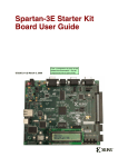
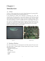
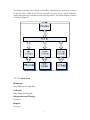
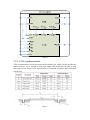
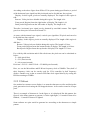
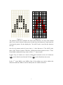
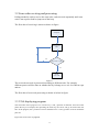
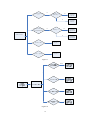
Text video Terminal
EDA385-Embedded system Design – Advanced Course
Ruiyi Zhang (sx07rz1)
Liding Zhao (sx07lz9)
Ling Ma (sx08ml4)
1
Abstract
This report documents the development of embedded video terminal that runs on a
Xilinx Spartan-3E FPGA (XC3S500E-4FG320C) FPGA on Spartan-3E Starter
Development Board. This project is developed under the environment of Xilinx ISE
and Platform Studio. The system includes Xilinx provided hardware, custom VHDL
IP and a Microblaze microprocessor, on which the c program were running. The
characters inputted by ps2 keyboard will be displayed on the VGA monitor.
2
Contents
1. Introduction.……………………………………………………………………..4
1.1 VT100…………………………………………………………………………………..4
1.2 Hardware platform……………………………………………………………………...4
1.3 Contribution……………………………………………………………………………..5
2. Hardware.………………………………………………………………………….6
2.1 PS/2 controller…………………………………………………………………………..6
2.2 VGA text controller……………………………………………………………………..6
2.2.1 VGA synchronization……………………………………………………………….....7
2.2.2 VGA text……………………………………………………………………………….8
3. Software.…………………………………………………………………………..12
3.1 Scan code……………………………………………………………………………….12
3.2 Scan code receiving and processing …………………………………………………....13
3.3 VGA displaying program………………………………………………………………..13
4. Conclusion………………………………………………………………………...15
4.1 Lesson learned…………………………………………………………………………...15
4.2 Further work……………………………………………………………………………..15
4.3 Installation and user manual……………………………………………………………..15
3
Chapter 1
Introduction
1.1 VT100
VT100 is a video terminal which was made by Digital Equipment Corporation (DEC).
It became the first standard used by terminal emulators [2].
It was introduced in August 1978, following its predecessor, the VT52, and
communicated with its host system over serial lines using the ASCII character set and
control sequences standardized by ANSI. The VT100 was also the first Digital
mass-market terminal to incorporate "graphic renditions" (blinking, bolding, reverse
video, and underlining) as well as a selectable 80 or 132 column display. All setup of
the VT100 was accomplished using interactive displays presented on the screen; the
setup data was stored in non-volatile memory within the terminal. The VT100 also
introduced an additional character set that allowed the drawing of on-screen forms.
Figure 1a shows the prototype of video terminal.
Figure 1a
Figure 1b [3]
1.2 Hardware Platform
The video terminal project was implemented on the Xilinx Spartan-3E starter board.
The target board is a Xilinx Spartan 3E Starter board shown in figure 1b with the
following specifications:
Microblaze microprocessor
BRAM
PS2 Controller
VGA Text Controller
UART
GPIO
4
The hardware architecture is based on PLB Bus. The Microbalze processor is master
of the bus, PS2, UART and VGA text controller are slave device. UART controller
connected to the hyper terminal is used as debug console. The block diagram is shown
as below in Figure 2.
Figure 2. Block diagram of Hardware
1.3 Contribution
Hardware:
Ruiyi Zhang and Liding Zhao
Software:
Ruiyi Zhang and Ling Ma
Integration and Testing:
Everyone
Report:
Everyone
5
Chapter 2
Hardware
2.1 PS/2 controller
PS/2 controller is used to receive scan code from ps/2 keyboard and the scan code is
written into memory mapped register. Microblaze processor can get the scan code
through read these registers. The keyboard uses a serial protocol with 11-bit frames,
as illustrated in figure. These bits are:
1 start bit. This is always 0.
●8 data bits, least significant bit first.
●1 parity bit (odd parity).
●1 stop bit. This is always 1.
Figure 3[1]
In this project, we use ps/2 controller of Xilinx IP core at last. Although we created
our own hardware of ps/2 controller, it is not very stable under polling mode. It would
be quite time consuming to debug it connected to PLB Bus. Therefore, we decided to
use Xilinx IP to save time to continue the project.
2.2 VGA text controller
The VGA port of Xilinx Spartan-3E starter board has five active signals, including the
horizontal and vertical synchronization signals, hsync and vsync, and three video
signals for the red, green, blue color. It is connected to a 15-pin D-sub connector to
display 8 different colors. The hsync and vsync signals are used to control the
horizontal and vertical scans of the monitor.
A VGA controller generates the synchronization signals and outputs data pixels
consequently. In our design, VGA controller is divided into two components:
synchronization circuit and text generation circuit. The first circuit generates the
timing and synchronization signals. The second one generates three RGB video
signals [4].
The VGA text controller block overview is show in figure 4.
6
Figure 4
2.2.1 VGA synchronization
VGA synchronization circuit generates the horizontal sync signal, which specifies the
time to traverse a row, and the vertical sync signal, which specifies the time to scan
the entire screen. In our VGA specification, a resolution of 640-by-480 with 60Hz
refresh rate.
Figure 5
7
According to the above figure from Xilinx VGA system timing specification, a period
of the horizontal sync signal has 800 pixels and can be divided into four regions:
Display: In this region, pixels are actually displayed. The length of this region is
640.
Retrace: Video pixels are disable during this region. The length is 96.
Front porch: Region forms the right border of display. The length is 16.
Back porch: Region forms the left border of display. The length is 48.
Therefore, horizontal sync signal can be obtained by mod-800 counter. This signal
goes low when pixel is between 656 and 751.
As same with horizontal sync signal, vertical sync signal has 521pixels and can also
be divided into four regions:
Display: In this region, pixels are actually displayed. The length of this region is
480 lines.
Retrace: Video pixels are disable during this region. The length is 2 lines.
Front porch: Region forms the bottom border of display. The length is 10 lines.
Back porch: Region forms the top border of display. The length is 33 lines.
For a 640-by-480 resolution and 60 Hz refresh rate, the pixel rate can be calculated as
below:
P = 800 (pixels/line)
L = 521 (lines/screen)
S = 60 (screens/second)
Pixel rate = P*L*S = 800*521*60 = 25.008M (pixel/second).
Here, we use the Microblaze and PLB bus frequency clock of 50MHz. Then, half of
their frequency clock can be exactly used for VGA controller by half frequency
divider. Another way is that to connect PLB Bus clock signal directly by setting the
PLB bus running at 25MHz.
2.2.2 VGA text
One method to construct a text display is to treat the characters as tiles and design the
pixel generation circuit using the tile-mapped scheme. A tile can be treated as a super
pixel.
There is a example of character A. In the figure a, A is displayed like this pattern, the
figure b is the binary pattern to generate A. In the right figure, ‘0’ stands for dots to be
blanked, ‘1’ stands for dots to be lighted.
Some software are quite useful to generate hex according to the characters or simple
pattern.
8
0
0
0
0
0
0
0
0
0
0
0
1
1
0
0
0
0
0
0
0
0
0
0
0
1
1
1
1
1
0
0
0
0
0
0
0
0
1
1
1
1
1
1
0
0
0
0
0
0
0
0
1
1
1
1
0
0
0
1
0
0
0
0
0
0
0
0
1
1
1
1
0
0
0
1
0
0
0
0
0
0
0
0
0
0
1
1
1
1
1
1
0
0
0
0
0
0
0
0
0
0
0
0
0
1
1
1
1
1
0
0
0
0
0
0
0
0
0
0
0
0
0
0
1
1
0
0
0
Figure 6 a
Figure 6 b
The patterns of the tiles constitute the font of the characters. An 8-by-16(8-column
and 16-row) font is chosen in this project. In this font, each character is represented as
8-by-16pixel pattern. For the display, the 7-bit ASCII code is used for the character
tiles [4].
One 8-by-16 pattern needs 16 bytes, that is, 2 7 bits. Because of 7-bit ASCII code,
there exist 2 7 kinds of pattern. Therefore, a ROM stored these patterns needs 214 bits.
If the ROM is addressed in byte, there will be 211 bytes in total.
If these 8-by-16 charters are used in 640-by-480 resolution screen, 80 characters
640
480
) can be fitted in one line and 30 lines (
) can be fitted into one screen.
(
8
16
In the 211 bytes ROM, seven MSBs of the 11-bits address are used to address the
characters and four LSBs are used to identify the row within a character.
9
Figure 7
Text circuit architecture is show in figure, it is made up two components. The first one
is dual port memory, which has one port for writing and one port for reading. The
writing port connected to PLB register.
Once Microblaze writing to this register in the four fields, that is x and y position of
character and ASCII code of character and write enable. This register can be set to 32
bits (bit 31 to 24 is stored for position y, bit 23 to 16 is stored for position x, bit 15 to
8 is stored for ASCII code, bit 7 to 0 is stored for write enable). As the figure shown,
in the writing port of memory, five bits of psn_y and seven bits of psn_x form twelve
bits address of writing and seven bits ASCII code is the data of input. Another address
of read port is connected to upper bits of pixel_x and pixel_y, which are generated by
synchronization circuit. The read output data is ASCII code of every saved character.
This character ASCII code together with three lowest bits of pixel_y is used to address
the byte of font ROM. In the last stage, three lowest bits of pixel_x is the input signal
of 8-to-1 MUX to select every pixel of this byte.
A cursor is included to mark to current location of entry and the cursor block keeps
the track of current location of cursor.
Table summarizes the resource utilization for PS/2 controller and VGA text controller
blocks created for this project.
10
PS/2 controller
Resources
Number of Slices
Number of Slice Flip Flops
Number of 4 input LUTs
Number of BRAMs
Used
275 out of 4656
370 out of 9312
421 out of 9312
0 out of 20
Utilization
5%
3%
4%
0%
Used
155 out of 4656
229 out of 9312
162 out of 9312
3 out of 20
Utilization
3%
2%
1%
15 %
VGA text controller
Resources
Number of Slices
Number of Slice Flip Flops
Number of 4 input LUTs
Number of BRAMs
We can see that most components of the VGA text controller hardware are RAM,
which are used as memory and ROM.
11
Chapter 3
Software
Based on hardware architecture, software mainly consists of two parts: one is that
PS/2 keyboard scan code receiving and processing program, the other one is VGA
displaying program.
3.1 Scan code
According to PS/2 keyboard specification, three types of key activities are observed:
●When a key is pressed, the make code of the key is transmitted.
●When a key is pressed down continuously, the make code is transmitted repeatedly
at a specific rate.
●When a key is released, the break code is transmitted.
For instance, when A is pressed and released, the keyboard first transmit its make
code and then the break code: 1C F0 1C.
As can be seen that 1C is the make code and F0 1C is the break code.
If we hold the key down for a while and then release it, the make code will be sent
several times: 1C 1C 1C … 1C F0 1C.
One case should be concerned is that multiple keys can be pressed at same time. For
example, @ character is obtained by pressed shift and 2. We can first press shift key
(scan code is 12) and then the 2 key (scan code 1E), and release 2 key and then shift
key. The total scan code sequence is 12 1E F0 1E F0 12.
Another case also needs concerned is that make code of some keys is four bytes
instead of two bytes, which are known is extended keys. For example upper arrow is
E0 75.
Upper case character can be obtained by two ways, one is that press shift key and
corresponding lower case key and then release them. Another way is that press and
release caps lock key first, then press the corresponding lower case key.
All the cases mentioned above are needed to treat differently. In the program,
normally we use judgement and flag to make them separately
12
3.2 Scan code receiving and processing
Polling method is used to receive the scan code, read scan code repeatedly until scan
code is not equal to 0x00 to jump out of the loop.
The flow char of receiving is shown as below in figure.
Setup PS/2
Receive Scan
Code
Yes
Scan Code == 0x00
No
Saving
Scan Code
Figure 8
The received scan code is processed according to different code. For example,
different process will be done on whether the key belongs to a-z or 0-9 or shift or caps
and etc.
The flow char of scan code processing is shown as below in figure.
3.3 VGA displaying program
The main idea of this program is to record every x and y position of character and cursor after
punch the key. For example, after punching the enter key, the cursor will go to head of the next
line. In the program, the x position of cursor should be set to 1 and y position of cursor should be
plus one.
Figure lists some cases of judgment.
13
Yes
Scan code is in the range of
a-z ?
Yes
Shift_flag == 1 or
Capslock_flag == 1?
Ascii code =
corresponding
small case
No
Yes
Scan code is in the range of
0-9, other printable char ?
Yes
Shift_flag == 1 ?
Switch (Scan code)
No
Scan code == shift ?
Shift_flag = 1
Scan code == caps lock ?
Caps_flag = 1
Figure 9
Figure 10
14
Ascii code =
corresponding
upper case
Ascii code =
corresponding
upper line char
Ascii code =
corresponding
lower line char
Chapter 4
Conclusion
The project was finished in fulfillment of the course requirements for EDA385,
Embedded Systems Advanced Course. It is a very good experience to learn embedded
system design and deeply get know to the methodology of hardware/software
co-design.
4.1 Lesson learned
1. Use Xilinx IP core as much as possible. Although building your own custom
hardware is challenging, you will has to face extra trouble and make more efforts to
meet very time-constraint project deadline.
2. If the component used is the IP core of ISE will not be recognized by EDK user_
logic because its library path is not known to specify.
In our project, one dual-port memory is used Xilinx-IP core of ISE and it works.
When it port to user_logic of EDK, this memory is not recognized because of the
library. One solution is to write VHDL code according to the template of dual-port
memory provided by Xilinx.
4.2 Further work
1. Implement text processing and editing program which would have the functions
such as copy and paste.
2. Make PS/2 mouse compatible.
4.3 Installation and user manual
1. Connect CRT displayer with VGA port and PS/2-based keyboard to the board.
2. Start Xilinx EDK 10.1, open the project file and download it to the FPGA.
3. After downloading, there should be a cursor on the VGA screen and then punch the keyboard to
input text. The keys in inside the red line rectangle of below picture are supported.
Figure 11
15
Bibliography
[1]Adam Chapweske. The PS/2 mouse/keyboard protocol.
http://www.computer-engineering.org/ps2protocol/, May 2003.
[2] VT100 User Guide. http://www.vt100.net/
[3] Spartan-3E Starter Kit Board User Guide
http://www.digilentinc.com/Data/Products/S3EBOARD/S3EStarter_ug230.pdf
[4]Pong P. Chu. FPGA Prototyping by VHDL Examples: Xilinx Spartan-3 Version.
Wiley, first edition, February 4, 2008.
16


![2008 [DAMN SMALL NAS]](http://vs1.manualzilla.com/store/data/005757702_2-ad0d2f1082977ee9ed587e807bbc0127-150x150.png)