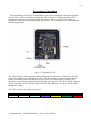
1
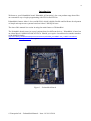
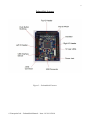
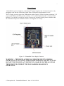
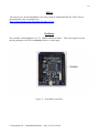
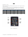
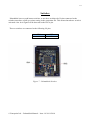
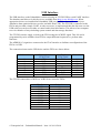
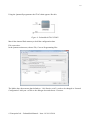
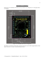
Polmaddie6 User Manual
Issue – 1.0
2
Foreword
PLEASE READ THIS ENTIRE MANUAL BEFORE PLUGGING IN
OR POWERING UP YOUR POLMADDIE6 BOARD.
PLEASE TAKE SPECIAL NOTE OF THE WARNINGS WITHIN
THIS MANUAL.
Trademarks
Altera, QuartusII, Max10 and NIOS are the registered trademarks of Altera Inc, San Jose,
California, US.
Polmaddie6 is a trademark of Enterpoint Ltd.
© Enterpoint Ltd. – Polmaddie6 Manual – Issue 1.0 20/11/2014
3
CONTENTS
Foreword
Trademarks
Introduction
Polmaddie6 Features
Getting Started
Polmaddie Features
Power Input
Io Headers
FPGA
Oscillator
Leds
Switches
USB Interface
Programming Polmaddie6
Mechanical Arrangement
Medical and Safety Critical Use
Warranty
Support
© Enterpoint Ltd. – Polmaddie6 Manual – Issue 1.0 20/11/2014
2
2
4
5
6
7
7
8
10
10
11
12
13
14
15
16
16
16
4
Introduction
Welcome to your Polmaddie6 board. Polmaddie is Enterpoint’s low cost product range that offers
an economical way to begin programming with FPGAs and FPGAs.
Polmaddie6 features Altera’s low cost MAX10, which is highly flexible and facilitates development
of simple microprocessor systems based on Altera’s NIOS processor.
The aim of this manual is to assist in using the main features of Polmaddie6.
The Polmaddie board comes in several variants based on different devices. Polmaddie6 is based on
an Altera Max10 10M08SAE144C8G FPGA. Should you require a board based on another member
of the MAX10 family:
http://www.altera.com/literature/br/br-max10-brochure.pdf?GSA_pos=6&WT.oss_r=1&WT.oss=max10
please contact Enterpoint sales for a quote.
Figure 1 – Polmaddie6 Board
© Enterpoint Ltd. – Polmaddie6 Manual – Issue 1.0 20/11/2014
5
Polmaddie6 features
Figure 2 – Polmaddie6 Features
© Enterpoint Ltd. – Polmaddie6 Manual – Issue 1.0 20/11/2014
6
Getting Started
Your Polmaddie6 will be supplied pre-programmed with a ‘traffic lights’ test design. The test
design will allow the user to determine that the LEDs and the push button switches of the
Polmaddie6 board are working. To use this test you should:
(1) Apply power to the Polmaddie6 board, either by connecting a 5V power supply to the 2.1mm
jack socket or by plugging a cable into the USB socket, either from a USB power supply adapter or
a PC.
(2) The LEDs should light in a ‘traffic lights’ sequence. There is also Power indicator LED which
will light to show that power is present and the 3.3V regulator is working.
(3) Press SW1 (This is the left Push Button switch). The traffic lights sequence will reset to the
beginning of the sequence.
(4) Press SW2 (This is the right Push Button switch). The traffic lights sequence will pause until the
switch is released.
© Enterpoint Ltd. – Polmaddie6 Manual – Issue 1.0 20/11/2014
7
Power Input
Polmaddie6 is powered either by connecting a 5V power supply to the 2.1mm jack socket or by
plugging a cable into the USB socket, either from a USB power supply adapter or a PC.
The 5V supply is used to power the USB interface and to supply a voltage regulator producing 3.3V
to power the FPGA, the LEDs and the oscillator. 3.3V is also available on pin 2 of each of the IO
headers. If you decide to use this as a source of power for external circuitry please remember that
the maximum total power available from the 3.3V Regulator is 2 Amps.
Figure 3 – Polmaddie6 Power Supply Features.
WARNING – THE REGULATORS MAY BECOME HOT IN NORMAL
OPERATION ALONG WITH THE BOARDS THERMAL RELIEF. PLEASE
DO NOT TOUCH OR PLACE HIGHLY FLAMABLE MATERIALS NEAR
THESE DEVICES WHILST THE POLMADDIE6 BOARD IS IN
OPERATION.
© Enterpoint Ltd. – Polmaddie6 Manual – Issue 1.0 20/11/2014
8
IO Headers
Figure 4 – Polmaddie6 Headers
The three 40-pin IDC Headers provide a simple mechanical and electrical interface for external
signal inputs. The connectors on this header are on a 0.1inch (2.54mm), pitch and allow other
electronic circuitry or user-designed add-on boards to be connected.
The headers each have 20 IOs routed to the FPGA. These are NOT 5V tolerant, the maximum
input voltage should be limited to 3.3V. IO21 is a dedicated Analog input. All the other IO can be
used as digital inputs or outputs. The headers each also have a permanent positive power pin on pin
2 and 19 permanent 0V connections as shown below:
Digital IO
Max10 digital IO are either High Speed or Low Speed. In the table below High Speed IO are shown
shaded blue (pins 26 to 119) and Low Speed IO are shaded yellow (pins 6-25 and 120-132). More
information about the IO specifications and capabilities is available from www.altera.com.
http://www.altera.co.uk/literature/lit-max-10.jsp
© Enterpoint Ltd. – Polmaddie6 Manual – Issue 1.0 20/11/2014
9
LEFT HEADER
PIN
1
3
5
7
9
11
13
15
17
19
21
23
25
27
29
31
33
35
37
39
USE
IO40
IO39
IO38
IO37
IO36
IO35
IO34
IO33
IO32
IO31
IO30
IO29*
IO28*
IO27*
IO26*
IO25*
IO24*
IO23*
IO22*
IO21*
FPGA
PIN
33
32
30
29
28
26
25
24
22
21
17
14
13
12
11
10
8
7
6
3
TOP HEADER
PIN
2
4
6
8
10
12
14
16
18
20
22
24
26
28
30
32
34
36
38
40
USE
3.3V
0V
0V
0V
0V
0V
0V
0V
0V
0V
0V
0V
0V
0V
0V
0V
0V
0V
0V
0V
PIN
1
3
5
7
9
11
13
15
17
19
21
23
25
27
29
31
33
35
37
39
USE
IO20
IO19
IO18
IO17
IO16
IO15
IO14
IO13
IO12
IO11
IO10
IO9
IO8
IO7
IO6
IO5
IO4
IO3
IO2
IO1
FPGA
PIN
132
131
130
127
124
123
120
119
118
115
114
113
112
111
110
101
100
99
98
97
RIGHT HEADER
PIN
2
4
6
8
10
12
14
16
18
20
22
24
26
28
30
32
34
36
38
40
USE
3.3V
0V
0V
0V
0V
0V
0V
0V
0V
0V
0V
0V
0V
0V
0V
0V
0V
0V
0V
0V
PIN
1
3
5
7
9
11
13
15
17
19
21
23
25
27
29
31
33
35
37
39
USE
IO60
IO59
IO58
IO57
IO56
IO55
IO54
IO53
IO52
IO51
IO50
IO49
IO48
IO47
IO46
IO45
IO44
IO43
IO42
IO41
FPGA
PIN
96
93
92
91
90
89
87
86
85
84
81
80
79
78
77
70
69
65
64
62
PIN
2
4
6
8
10
12
14
16
18
20
22
24
26
28
30
32
34
36
38
40
USE
3.3V
0V
0V
0V
0V
0V
0V
0V
0V
0V
0V
0V
0V
0V
0V
0V
0V
0V
0V
0V
*these signals have series 470 resistors and 10pf capacitors to ground so they can be used as analog
inputs.
Analog Inputs
The Max10 device has one dedicated analog input (IO21) and eight optional analog/digital IO.
When they are used for analog signals IO 22 to 29 are single ended inputs connecting to a 12 bit
ADC with a maximum sampling rate of 1MHz. The maximum input voltage is 3.3V. More
information about the Max10 analog capability can be found in
http://www.altera.co.uk/literature/hb/max-10/ug_m10_adc.pdf from www.altera.com.
© Enterpoint Ltd. – Polmaddie6 Manual – Issue 1.0 20/11/2014
10
FPGA
The main device on the Polmaddie6 is the Altera Max10 10M08SAE144C8G FPGA. Device
documentation can be obtained from:
http://www.altera.co.uk/literature/lit-max-10.jsp
Oscillator
The oscillator on Polmaddie6 is a 3.3V, 25MHz ASEM oscillator. This clock signal is routed
directly through to the FPGA on Pin 88, which is a clock input.
Figure 5 – Polmaddie6 Oscillator
© Enterpoint Ltd. – Polmaddie6 Manual – Issue 1.0 20/11/2014
11
LEDs
Polmaddie6 has 13 LEDs.
LED 1 is a green power indicator LED and indicates the presence of the 3.3V supply. It cannot be
controlled by the FPGA.
LEDs 2 to 13 are arranged in 4 blocks of three, each block having one red, one orange and one
green LED. This means they can be used to simulate traffic lights. They are all controlled by the
FPGA. They connect to the FPGA as shown below:
LED
LED4
LED2
LED3
LED7
LED5
LED6
FPGA PIN
41
39
38
135
138
141
COLOUR
RED
ORANGE
GREEN
RED
ORANGE
GREEN
LED
LED10
LED8
LED9
LED13
LED11
LED12
Figure 6 – Polmaddie6 LEDs
© Enterpoint Ltd. – Polmaddie6 Manual – Issue 1.0 20/11/2014
FPGA PIN
74
75
76
106
105
102
COLOUR
RED
ORANGE
GREEN
RED
ORANGE
GREEN
12
Switches
Polmaddie6 has two push button switches; to use these switches the IO pins connected to the
switches must have a pull up resistor setting in the constraints file. This means that when a switch is
activated a low level signal will be detected on the FPGA pin.
.
The two switches are connected to the following IO pins:
SW1
66
SW2
50
Figure 7 – Polmaddie6 Switches
© Enterpoint Ltd. – Polmaddie6 Manual – Issue 1.0 20/11/2014
13
USB Interface
The USB interface on the Polmaddie6 is achieved using an FT232H USB to serial UART interface.
The datasheet and drivers for this device are available from http://www.ftdichip.com. When
appropriate drivers are installed the Polmaddie6 USB port should be detected as a serial port.
Alternative data optimised drivers are also available from FTDI. The FT232H is connected to the
FPGA and provided a simple UART, or other converter, is implemented then the data sent over the
USB serial port can be used either as control and/or data information. This allows a host computer
to act in a number of ways including system control and data storage functions.
The FT232H can also supply a clock to the FPGA using the ACBUS5 signal. This I/O can be
programmed by tools available from FTDI to output different frequencies or perform other
functions.
The ADBUS(0:3) signals are connected to the JTAG interface to facilitate reconfiguration of the
FPGA via USB.
The connections between the USB device and the FPGA are shown below:
FT232H PIN
16
19
18
20
15
17
13
14
FT232H PORT
FUNCTION
CTS#
DCD#
DSR#
RI#
RTS#
DTR#
TXD
RXD
JTAG
FUNCTION
TMS
TDO
TCK
TDI
The FT232R connections ACBUS0 to ACBUS9 are routed to FPGA:
FT232R
ACBUS0
ACBUS1
ACBUS2
ACBUS3
ACBUS4
ACBUS5
ACBUS6
ACBUS7
ACBUS8
ACBUS9
FPGA PIN
56
55
54
52
51
27
46
45
44
43 (JTAG_ENABLE)
© Enterpoint Ltd. – Polmaddie6 Manual – Issue 1.0 20/11/2014
FPGA PIN
16
58
59
57
20
60
18
19
14
Programming Polmaddie6
The programming of the FPGA on Polmaddie6 can be achieved using the Altera tool QuartusII.
Version 4.0.2 or later is required to program the Max 10 device. It is anticipated that a JTAG
connection will be used in conjunction with this software. There is a single JTAG chain on
Polmaddie6 which allows the programming of the FPGA. We recommend you use the Enterpoint
PROG4 programmer.
Figure 8– Polmaddie6 JTAG
The JTAG interface can be enabled to allow configuration to take place or disabled to allow the
JTAG pins to function as USB signals or GPIO. This functionality is selected using the jumper
header J4. With the jumper fitted to the lower two pins JTAG functionality is selected. For
alternative uses the jumper must be fitted to the upper two pins of J4. This JTAG enable signal can
also be controlled via the ACBUS9 signal of the FT232H USB device, in which case the jumper
should not be fitted.
The JTAG connector has a layout as follows:
GND
NC (pin14)
GND
NC
GND
TDI
GND
TDO
GND
TCK
© Enterpoint Ltd. – Polmaddie6 Manual – Issue 1.0 20/11/2014
GND
TMS
GND (pin1)
3.3V
15
Using the QuartusII programmer the JTAG chain appears like this:
Figure 9– Polmaddie6 JTAG CHAIN
Max10 has internal flash memory to hold the configuration data.
File conversion:
In the Quartus main menu, choose File, Convert Programming files.
The Mode drop-down menu (that defaults to ‘1-bit Passive serial’) needs to be changed to ‘Internal
Configuration. Add your .sof file to the dialogue box and choose ‘Generate.
© Enterpoint Ltd. – Polmaddie6 Manual – Issue 1.0 20/11/2014
16
Mechanical Arrangement
Dimensions are in millimetres. The three 40-way connectors are arranged on a 0.1 inch grid relative
to eachother.
Figure 10– Polmaddie6 Mechanical Arrangement
The PCB is 1.6mm thick and the tallest component is the power jack which is approximately 11mm
high. Dimensions are subject to manufacturing tolerances.
© Enterpoint Ltd. – Polmaddie6 Manual – Issue 1.0 20/11/2014
17
Medical and Safety Critical Use
Polmaddie6 boards are not authorised for the use in, or use in the design of, medical or other safety
critical systems without the express written person of the Board of Enterpoint. If such use is
allowed the said use will be entirely the responsibility of the user. Enterpoint Ltd will accepts no
liability for any failure or defect of the Polmaddie6 board, or its design, when it is used in any
medical or safety critical application
Warranty
Polmaddie6 comes with a 90 return to base warranty. Enterpoint reserves the right not honour a
warranty if the failure is due to maltreatment of the Polmaddie6 board.
Outside the warranty period Enterpoint offers a fixed price repair or replacement service. We
reserve the right not to offer this service where a Polmaddie6 has been maltreated or otherwise
deliberately damaged. Please contact support if need to use this service.
Other specialised warranty programs can be offered to users of multiple Enterpoint products.
Please contact sales on [email protected] if you are interested in these types of warranty,
Support
Enterpoint offers support during normal United Kingdom working hours 9.00am to 5.00pm. Please
examine our Polmaddie6 FAQ web page and the contents of this manual before raising a support
query. We can be contacted as follows:
Telephone
Email
- +44 (0) 121 288 3945
- [email protected]
© Enterpoint Ltd. – Polmaddie6 Manual – Issue 1.0 20/11/2014