1
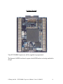
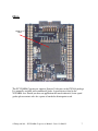
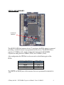
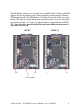
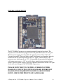
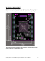
XC3S3400A Coprocessor User Manual
Issue – 1.0
© Enterpoint Ltd. – XC3S3400A Coprocessor Manual – Issue 1.0 10/6/12
1
Programming Cable
You will need a programming cable to connect between your PC and the
XC3S3400A Coprocessor board. The Enterpoint PROG3 cable is recommended, or if
you have a parallel port on your PC the Enterpoint PROG2 cable can be used.
Foreword
PLEASE READ THIS ENTIRE MANUAL BEFORE PLUGGING IN
OR POWERING UP YOUR XC3S3400A COPROCESSOR BOARD.
PLEASE TAKE SPECIAL NOTE OF ANY WARNINGS WITHIN
THIS MANUAL.
Trademarks
Spartan-3A, ISE, Webpack, Xilinx are the registered trademarks of Xilinx Inc, San Jose,
California, US.
© Enterpoint Ltd. – XC3S3400A Coprocessor Manual – Issue 1.0 10/6/12
2
Contents
Programming Cable
Foreword
Trademarks
XC3S3400A Coprocessor Board
Introduction
Getting Started
FPGA
SPI FLASH
DIL HEADERS
LEDS
CLOCK
POWER CONNECTIONS
POWER REGULATORS
CONFIGURATION JUMPER SETTINGS
PROGRAMMING XC3S3400A Coprocessor
Mechanical Arrangement
Medical and Safety Critical Use
Warranty
Support
© Enterpoint Ltd. – XC3S3400A Coprocessor Manual – Issue 1.0 10/6/12
2
2
2
4
5
6
7
8
10
12
13
14
15
16
17
19
20
20
20
3
XC3S3400A Coprocessor
© Enterpoint Ltd. – XC3S3400A Coprocessor Manual – Issue 1.0 10/6/12
4
Introduction
Welcome to your XC3S3400A Coprocessor board. This board is primarily intended
to extend the processing capabilities of any of the Enterpoint Xilinx based
development boards, e.g. Raggedstone 1 and 2, Broaddown 2 and 4 or Drigmorn 2, 3
and 4. However it could also be used to extend the capabilities of a user's own board
which has suitable headers and power supply arrangement.
The aim of this manual is to assist in using the main features of XC3S3400A
Coprocessor.
There are features that are beyond the scope of the manual. Should you need to use
these features then please email [email protected] for detailed instructions.
XC3S3400A Coprocessor currently comes with a XC3S3400A-4CSG484CD
Spartan-3A. A variant based on the XC3S1800A device may be offered at a later date
or as an OEM product. Please contact out us on [email protected] should you
need further information.
© Enterpoint Ltd. – XC3S3400A Coprocessor Manual – Issue 1.0 10/6/12
5
Getting Started
Your XC3S3400A Coprocessor will be supplied un-programmed.
The Spartan-3A FPGA on board requires the full ISE toolset to develop and build a
design.
© Enterpoint Ltd. – XC3S3400A Coprocessor Manual – Issue 1.0 10/6/12
6
FPGA
SPARTAN-3A
FPGA
The XC3S3400A Coprocessor supports Spartan-3A devices in the CSG484 package.
It is normally available with commercial grade -4 speed devices fitted in the
X3S3400A size. Should you have an application that needs industrial, faster speed
grades please contact sales for a quote at [email protected].
© Enterpoint Ltd. – XC3S3400A Coprocessor Manual – Issue 1.0 10/6/12
7
SPI FLASH MEMORY
128M FLASH
MEMORY
The M25P128 SPI flash memory device U3 configures the FPGA when it is powered
providing a suitable bitstream is programmed into the device. The M25P128 has a
capacity of 128Mbits with a single configuration bitstream for XC3S3400A
Coprocessor taking between 3.6Mbits (LX16) and 11.4Mbits (LX45).
After configuration the SPI Flash can be accessed via the following pins of the
FPGA:
M25P128 FUNCTION
CCLK
MOSI
DIN
CSO_B
FPGA PIN
V17
V13
W17
U7
The WRITE and HOLD pins of this memory device are permanently connected to
3.3V.
© Enterpoint Ltd. – XC3S3400A Coprocessor Manual – Issue 1.0 10/6/12
8
The M25P128 SPI flash memory device can also be accessed from a host board via
pins RHS2 to RHS5 if the correct link is made on J5.
Pin6
ISSUE 1.1 board
Pin1
Fitting the link between pins 1 and 6 maps the SPI Flash signals as shown below:
RHS DIL HEADER PIN
2
3
4
5
JTAG Signal
DIN(U3 pin 2)
MOSI(U3 pin 5)
CSO_B (U3 pin 1)
CCLK (U3 pin6)
An adapter is available to facilitate the jumper settings on version 1.0
of this board. This is not necessary for version 1.1.
© Enterpoint Ltd. – XC3S3400A Coprocessor Manual – Issue 1.0 10/6/12
9
DIL HEADERS
The DIL Headers provide a simple mechanical and electrical interface for connecting
the XC3S3400A coprocessor module to a supporting board. There are twenty I/O on
each side of the DIL Header giving a total of 40 possible I/O.
LEFT COLUMNS
OUTER PINS
INN
ER
S3
ROW FUNCTION PIN PINS
1
IO_L05N_0 AB6
0V
2
IO_L05P_0 AB5
0V
3
IO_L08N_2 AA8
0V
4
IO_L08P_2 AB7
0V
5
IO_L12N_2 AA10
0V
6
IO_L12P_2 AB10
0V
7
IO_L02N_1 AA22
0V
8
IO_L02P_1
Y21
0V
9
IO_L06N_1 Y22
0V
10
IO_L06P_1 W22
0V
11
IO_L14N_1
P22
0V
12
IO_L14P_1
R22
0V
13
IO_L28N_1 G22
0V
14
IO_L28P_1
H22
0V
15
IO_L37N_1 D22
0V
16
IO_L37P_1
D21
0V
17
IO_L1N_0
C19
0V
18
IO_L1P_0
D19
0V
19
IO_L7N_0
A19
0V
20
IO_L7P_0
B20
0V
RIGHT COLUMNS
OUTER PINS
INNER
S3
PINS FUNCTION PIN
3.3V
IO_L04N_2 AA4
3.3V
IO_L04P_2 AB4
3.3V
IO_L35N_3
W1
3.3V
IO_L35P_3
Y1
3.3V
IO_L33N_3
V1
3.3V
IO_L33P_3
U2
3.3V
IO_L30N_3
U1
3.3V
IO_L30P_3
T1
3.3V
IO_L28N_3
R1
3.3V
IO_L28P_3
R2
3.3V
IO_L25N_3
P2
3.3V
IO_L25P_3
P1
3.3V
IO_L22N_3
N1
3.3V
IO_L22P_3
M1
3.3V
IO_L14N_3
J1
3.3V
IO_L14P_3
H2
3.3V
IO_L11N_3
H1
3.3V
IO_L11P_3
G1
3.3V
IO_L06N_3
F1
3.3V
IO_L06P_3
F2
These DIL Headers can support up 20 pairs of LVDS signalling. The Spartan-3A
FPGA can terminate any of these pairs as inputs. True differential output standards
are supported only on FPGA banks 0 and 2. See Xilinx datasheet ds610.pdf available
from www.xilinx.com . LVDS termination on individual signal pairs is a
programmable option that can be set in build constraints for the FPGA when using
the ISE toolset. The LVDS pairs are shown in the table above along with their bank
numbers and the Spartan-3A pin numbers.
© Enterpoint Ltd. – XC3S3400A Coprocessor Manual – Issue 1.0 10/6/12
10
The DIL Header connectors are arranged on a standard 0.1inch (2.54mm) pitch. This
supports the use of prototype circuits using stripboard or other prototype materials.
The horizontal pitch of the DIL Headers is 1.6 inches between the outer rows of the
headers. The inner pins of the header form continuous power strips, one side header
has an inner column of 3.3V pins. The other header has an inner column of DGND
(0V). Note the voltage on each side of the header pins differs between issue 1.0
and issue 1.1 of this pcb
ISSUE 1
3.3V
ISSUE 1.1
0V
0V
3.3V
Issue number
© Enterpoint Ltd. – XC3S3400A Coprocessor Manual – Issue 1.0 10/6/12
11
LEDS
LED3
LED2
LED1
XC3S3400A Coprocessor has 3 LEDs. These are arranged in a block to the left of the
FPGA. The uppermost LED is Red, the centre one is Orange and the lowest one is
green. The LEDS will turn on dimly when power is applied to the board. The relevant
IO pin for an LED needs to be asserted high to ensure the specific LED turns on.
The LEDS are connected to the FPGA as indicated below:
LED
1
2
3
FPGA PIN
M2
L1
L3
COLOUR
GREEN
ORANGE
RED
© Enterpoint Ltd. – XC3S3400A Coprocessor Manual – Issue 1.0 10/6/12
12
CLOCK
It will be necessary for the user to arrange a clock source for the FPGA. If this board
is plugged into an Enterpoint development board it is simply a case of routing the
clock on that board to one of the IOs on the DIL headers supporting this module.
Alternatively a 3.3V oscillator can be connected to one of the input pins from your
own circuitry.
© Enterpoint Ltd. – XC3S3400A Coprocessor Manual – Issue 1.0 10/6/12
13
POWER CONNECTIONS
The XC3S3400A Coprocessor is powered principally from the host board. The
Coprocessor board should be plugged into 0.1mm pitch DIL headers on a host pcb.
The host power supply must be capable of supplying at least 1A at 3.3V to the
Coprocessor module. The actual power supply requirements are dependent upon the
demands of the IOs which operate from the 3.3V supply, and the design in the
processor core, which operates at 1.2V. A demanding design running at high speed
will require more power at 1.2V (up to 4A) than a simple design running at lower
speeds. Whatever power supply is used care should be taken not to exceed 5.4V input
as this will cause damage to the XC3S3400A Coprocessor.
PLEASE NOTE THAT TO USE THE 1.0 VERSION OF THIS
BOARD IN CONJUNCTION WITH STANDARD ENTERPOINT
BOARDS WILL REQUIRE IT TO BE PLUGGED IN UPSIDE
DOWN. CHECK THE PINOUTS OF EACH BOARD.
© Enterpoint Ltd. – XC3S3400A Coprocessor Manual – Issue 1.0 10/6/12
14
POWER REGULATOR
1.2V REGULATOR
A Micrel MI22600 regulator supplies 1.2V with a maximum current available of 6A
(In practice this may be limited by the power available from the 3.3Vsupply from the
host board).
WARNING – REGULATORS CAN BECOME HOT IN NORMAL
OPERATION ALONG WITH THE BOARDS THERMAL RELIEF. PLEASE
DO NOT TOUCH OR PLACE HIGHLY FLAMABLE MATERIALS NEAR
THESE DEVICES WHILST THE XC3S3400A Coprocessor BOARD IS IN
OPERATION.
© Enterpoint Ltd. – XC3S3400A Coprocessor Manual – Issue 1.0 10/6/12
15
CONFIGURATION JUMPER SETINGS
The XC3S3400A module can be programmed in two ways. The first is to use the
JTAG connector J2, which is a 7x2 2mm Right angled shrouded male header.
Alternatively the JTAG connections can be accessed from the host board via the DIL
header pins. Using this approach some of the IO on the DIL header will be
unavailable while configuration is taking place.
Jumper J5 is used to select whether the JTAG signal source is the connector J2 or the
DIL headers pins RHS2 to RHS5
ISSUE 1.1 board
Pin4
Pin3
J5 LINK
None
Pins 3 to 4
JTAG SOURCE
J2
RHS2 to RHS5
Fitting the link between pins 3 and 4 maps the JTAG signals as shown below:
RHS DIL HEADER PIN
2
3
4
5
JTAG Signal
TDI
TDO
TCK
TMS
An adapter is available to facilitate the jumper settings on version 1.0
of this board. This is not necessary for version 1.1.
© Enterpoint Ltd. – XC3S3400A Coprocessor Manual – Issue 1.0 10/6/12
16
Programming XC3S3400A Coprocessor
The programming of the FPGA and SPI Flash part on XC3S3400A Coprocessor is
achieved using the JTAG interface.
There is a single JTAG chain on XC3S3400A Coprocessor. The JTAG chain allows
the programming of the Spartan-3A and SPI Flash device.
The JTAG connector has a layout as follows (top view):
3V3
GND
TMS
GND
TCK
GND
TDO
GND
TDI
GND
NC
GND
NC
GND
Using iMPACT Boundary Scan the JTAG chain appears like this:
1. Programming the FPGA directly.
Direct JTAG programming of the Spartan-3A FPGA is volatile and the FPGA will
lose its configuration every time the board power is cycled. For sustained use of an
FPGA design programming the design into the Flash memory is recommended (see 2
and 3 below).
Direct JTAG programming using .bit files is useful for fast, temporary programming
during development of FPGA programs. Right click the icon representing the
Spartan-3A FPGA and choose ‘Assign New Configuration File’. Navigate to your .bit
file and choose ‘OPEN’. The next dialogue box will offer to add a flash memory and
you should decline. Right click the icon representing the Spartan-3A FPGA and
choose ‘Program’. On the next dialogue box ensure that the ‘Verify’ box is not
checked. (If it is you should uncheck it, failure to do this will result in error messages
being displayed). Click OK. The Spartan-6 will program. This process is very quick
(typically one second)
© Enterpoint Ltd. – XC3S3400A Coprocessor Manual – Issue 1.0 10/6/12
17
2. Programming the SPI flash memory using Boundary Scan.
Once the SPI Flash memory has been programmed, the Spartan-3A device will
automatically load from the Flash memory at power up. Generation of suitable Flash
memory files (.mcs) can be achieved using ISE iMPACT’s Prom File Formatter.
Right click on the icon representing the Spartan-3A and choose ‘Add SPI/BPI Flash’
Navigate to your programming file (.mcs) and click OPEN. Use the next dialogue
box to select SPI flash and M25P128. Data width should be set to 1. The flash
memory should appear as shown below.
Right click on the icon representing the flash memory and choose program to load
your program into the device. It is recommended that options to ‘Verify’ and ‘Erase
before programming’ are chosen. Otherwise all defaults can be accepted. The
programming operation will take some time (at least 3 or 4 minutes)
© Enterpoint Ltd. – XC3S3400A Coprocessor Manual – Issue 1.0 10/6/12
18
MECHANICAL ARRANGEMENT
The Dimensions on the drawing below are millimetres (mm). All sizes quoted are
subject to manufacturing tolerances and should only be used as a general guide.
The height of the highest components (the header pins), measured from the lower
surface of the board, is approximately 7mm.
© Enterpoint Ltd. – XC3S3400A Coprocessor Manual – Issue 1.0 10/6/12
19
Medical and Safety Critical Use
XC3S3400A Coprocessor boards are not authorised for the use in, or use in the
design of, medical or other safety critical systems without the express written person
of the Board of Enterpoint. If such use is allowed the said use will be entirely the
responsibility of the user. Enterpoint Ltd will accepts no liability for any failure or
defect of the XC3S3400A Coprocessor board, or its design, when it is used in any
medical or safety critical application.
Warranty
XC3S3400A Coprocessor comes with a 90 day return to base warranty. Do not
attempt to solder connections to the XC3S3400A Coprocessor. Enterpoint reserves
the right not honour a warranty if the failure is due to soldering or other maltreatment
of the XC3S3400A Coprocessor board.
Outside warranty Enterpoint offers a fixed price repair or replacement service. We
reserve the right not to offer this service where a XC3S3400A Coprocessor has been
maltreated or otherwise deliberately damaged. Please contact support if you need to
use this service.
Other specialised warranty programs can be offered to users of multiple Enterpoint
products. Please contact sales on [email protected] if you are interested in
these types of warranty,
Support
Telephone and email support is offered during normal United Kingdom working
hours (GMT or GMT + 1) 9.00am to 5.00pm.
Telephone - +44 (0) 121 288 3945
Email
- [email protected]
© Enterpoint Ltd. – XC3S3400A Coprocessor Manual – Issue 1.0 10/6/12
20


![Atari ST System-on-Chip in VHDL (Author: Lyndon Amsdon) [undated]](http://vs1.manualzilla.com/store/data/005994841_1-cb1a0817df59f22c671df08194997a7c-150x150.png)