1
80C186EC/80C188EC
Microprocessor
User’s Manual
80C186EC/80C188EC
Microprocessor
User’s Manual
1995
Information in this document is provided solely to enable use of Intel products. Intel assumes no liability whatsoever, including
infringement of any patent or copyright, for sale and use of Intel products except as provided in Intel’s Terms and Conditions
of Sale for such products.
Intel Corporation makes no warranty for the use of its products and assumes no responsibility for any errors which may appear
in this document nor does it make a commitment to update the information contained herein.
Intel retains the right to make changes to these specifications at any time, without notice.
Contact your local Intel sales office or your distributor to obtain the latest specifications before placing your product order.
MDS is an ordering code only and is not used as a product name or trademark of Intel Corporation.
Intel Corporation and Intel's FASTPATH are not affiliated with Kinetics, a division of Excelan, Inc. or its FASTPATH trademark
or products.
*Other brands and names are the property of their respective owners.
Additional copies of this document or other Intel literature may be obtained from:
Intel Corporation
Literature Sales
P.O. Box 7641
Mt. Prospect, IL 60056-7641
or call 1-800-879-4683
© INTEL CORPORATION, 1995
CONTENTS
CHAPTER 1
INTRODUCTION
1.1
HOW TO USE THIS MANUAL....................................................................................... 1-2
1.2
RELATED DOCUMENTS .............................................................................................. 1-3
1.3
ELECTRONIC SUPPORT SYSTEMS ........................................................................... 1-4
1.3.1
FaxBack Service .......................................................................................................1-4
1.3.2
Bulletin Board System (BBS) ....................................................................................1-5
1.3.2.1
How to Find ApBUILDER Software and Hypertext Documents on the BBS ...1-6
1.3.3
CompuServe Forums ................................................................................................1-6
1.3.4
World Wide Web .......................................................................................................1-6
1.4
TECHNICAL SUPPORT ................................................................................................ 1-6
1.5
PRODUCT LITERATURE.............................................................................................. 1-7
1.6
TRAINING CLASSES .................................................................................................... 1-7
CHAPTER 2
OVERVIEW OF THE 80C186 FAMILY ARCHITECTURE
2.1
ARCHITECTURAL OVERVIEW .................................................................................... 2-1
2.1.1
Execution Unit ...........................................................................................................2-2
2.1.2
Bus Interface Unit .....................................................................................................2-3
2.1.3
General Registers .....................................................................................................2-4
2.1.4
Segment Registers ...................................................................................................2-5
2.1.5
Instruction Pointer .....................................................................................................2-6
2.1.6
Flags .........................................................................................................................2-7
2.1.7
Memory Segmentation ..............................................................................................2-8
2.1.8
Logical Addresses ...................................................................................................2-10
2.1.9
Dynamically Relocatable Code ...............................................................................2-13
2.1.10 Stack Implementation .............................................................................................2-15
2.1.11 Reserved Memory and I/O Space ...........................................................................2-15
2.2
SOFTWARE OVERVIEW ............................................................................................ 2-17
2.2.1
Instruction Set .........................................................................................................2-17
2.2.1.1
Data Transfer Instructions .............................................................................2-18
2.2.1.2
Arithmetic Instructions ...................................................................................2-19
2.2.1.3
Bit Manipulation Instructions .........................................................................2-21
2.2.1.4
String Instructions ..........................................................................................2-22
2.2.1.5
Program Transfer Instructions .......................................................................2-23
2.2.1.6
Processor Control Instructions ......................................................................2-27
2.2.2
Addressing Modes ..................................................................................................2-27
2.2.2.1
Register and Immediate Operand Addressing Modes ...................................2-27
2.2.2.2
Memory Addressing Modes ...........................................................................2-28
2.2.2.3
I/O Port Addressing .......................................................................................2-36
2.2.2.4
Data Types Used in the 80C186 Modular Core Family .................................2-37
iii
CONTENTS
2.3
INTERRUPTS AND EXCEPTION HANDLING ............................................................ 2-39
2.3.1
Interrupt/Exception Processing ...............................................................................2-39
2.3.1.1
Non-Maskable Interrupts ...............................................................................2-42
2.3.1.2
Maskable Interrupts .......................................................................................2-42
2.3.1.3
Exceptions .....................................................................................................2-42
2.3.2
Software Interrupts ..................................................................................................2-44
2.3.3
Interrupt Latency .....................................................................................................2-44
2.3.4
Interrupt Response Time ........................................................................................2-45
2.3.5
Interrupt and Exception Priority ...............................................................................2-46
CHAPTER 3
BUS INTERFACE UNIT
3.1
MULTIPLEXED ADDRESS AND DATA BUS ................................................................ 3-1
3.2
ADDRESS AND DATA BUS CONCEPTS ..................................................................... 3-1
3.2.1
16-Bit Data Bus .........................................................................................................3-1
3.2.2
8-Bit Data Bus ...........................................................................................................3-5
3.3
MEMORY AND I/O INTERFACES................................................................................. 3-6
3.3.1
16-Bit Bus Memory and I/O Requirements ...............................................................3-7
3.3.2
8-Bit Bus Memory and I/O Requirements .................................................................3-7
3.4
BUS CYCLE OPERATION ............................................................................................ 3-7
3.4.1
Address/Status Phase ............................................................................................3-10
3.4.2
Data Phase .............................................................................................................3-13
3.4.3
Wait States ..............................................................................................................3-13
3.4.4
Idle States ...............................................................................................................3-18
3.5
BUS CYCLES .............................................................................................................. 3-20
3.5.1
Read Bus Cycles ....................................................................................................3-20
3.5.1.1
Refresh Bus Cycles .......................................................................................3-22
3.5.2
Write Bus Cycles .....................................................................................................3-23
3.5.3
Interrupt Acknowledge Bus Cycle ...........................................................................3-26
3.5.3.1
System Design Considerations .....................................................................3-28
3.5.4
HALT Bus Cycle ......................................................................................................3-29
3.5.5
Temporarily Exiting the HALT Bus State .................................................................3-32
3.5.6
Exiting HALT ...........................................................................................................3-34
3.6
SYSTEM DESIGN ALTERNATIVES ........................................................................... 3-36
3.6.1
Buffering the Data Bus ............................................................................................3-37
3.6.2
Synchronizing Software and Hardware Events .......................................................3-39
3.6.3
Using a Locked Bus ................................................................................................3-40
3.7
MULTI-MASTER BUS SYSTEM DESIGNS................................................................. 3-41
3.7.1
Entering Bus HOLD ................................................................................................3-41
3.7.1.1
HOLD Bus Latency ........................................................................................3-42
3.7.1.2
Refresh Operation During a Bus HOLD ........................................................3-43
3.7.2
Exiting HOLD ..........................................................................................................3-45
3.8
BUS CYCLE PRIORITIES ........................................................................................... 3-46
iv
CONTENTS
CHAPTER 4
PERIPHERAL CONTROL BLOCK
4.1
PERIPHERAL CONTROL REGISTERS........................................................................ 4-1
4.2
PCB RELOCATION REGISTER.................................................................................... 4-1
4.3
RESERVED LOCATIONS ............................................................................................. 4-4
4.4
ACCESSING THE PERIPHERAL CONTROL BLOCK .................................................. 4-4
4.4.1
Bus Cycles ...............................................................................................................4-4
4.4.2
READY Signals and Wait States .............................................................................4-4
4.4.3
F-Bus Operation .......................................................................................................4-5
4.4.3.1
Writing the PCB Relocation Register ...............................................................4-6
4.4.3.2
Accessing the Peripheral Control Registers ....................................................4-6
4.4.3.3
Accessing Reserved Locations .......................................................................4-6
4.5
SETTING THE PCB BASE LOCATION......................................................................... 4-6
4.5.1
Considerations for the 80C187 Math Coprocessor Interface ....................................4-7
CHAPTER 5
CLOCK GENERATION AND POWER MANAGEMENT
5.1
CLOCK GENERATION.................................................................................................. 5-1
5.1.1
Crystal Oscillator .......................................................................................................5-1
5.1.1.1
Oscillator Operation .........................................................................................5-2
5.1.1.2
Selecting Crystals ............................................................................................5-5
5.1.2
Using an External Oscillator ......................................................................................5-6
5.1.3
Output from the Clock Generator ..............................................................................5-6
5.1.4
Reset and Clock Synchronization .............................................................................5-6
5.2
POWER MANAGEMENT............................................................................................. 5-10
5.2.1
Idle Mode ................................................................................................................5-11
5.2.1.1
Entering Idle Mode ........................................................................................5-11
5.2.1.2
Bus Operation During Idle Mode ...................................................................5-13
5.2.1.3
Leaving Idle Mode .........................................................................................5-14
5.2.1.4
Example Idle Mode Initialization Code ..........................................................5-15
5.2.2
Powerdown Mode ...................................................................................................5-16
5.2.2.1
Entering Powerdown Mode ...........................................................................5-17
5.2.2.2
Leaving Powerdown Mode ............................................................................5-18
5.2.3
Power-Save Mode ..................................................................................................5-19
5.2.3.1
Entering Power-Save Mode ..........................................................................5-20
5.2.3.2
Leaving Power-Save Mode ...........................................................................5-22
5.2.3.3
Example Power-Save Initialization Code .......................................................5-22
5.2.4
Implementing a Power Management Scheme ........................................................5-24
CHAPTER 6
CHIP-SELECT UNIT
6.1
COMMON METHODS FOR GENERATING CHIP-SELECTS....................................... 6-1
6.2
CHIP-SELECT UNIT FEATURES AND BENEFITS ...................................................... 6-1
6.3
CHIP-SELECT UNIT FUNCTIONAL OVERVIEW ......................................................... 6-2
v
CONTENTS
6.4
PROGRAMMING ........................................................................................................... 6-5
6.4.1
Initialization Sequence ..............................................................................................6-6
6.4.2
Start Address ..........................................................................................................6-10
6.4.3
Stop Address ..........................................................................................................6-10
6.4.4
Enabling and Disabling Chip-Selects ......................................................................6-11
6.4.5
Bus Wait State and Ready Control .........................................................................6-11
6.4.6
Overlapping Chip-Selects .......................................................................................6-12
6.4.7
Memory or I/O Bus Cycle Decoding ........................................................................6-14
6.4.8
Programming Considerations ..................................................................................6-14
6.5
CHIP-SELECTS AND BUS HOLD............................................................................... 6-15
6.6
EXAMPLES ................................................................................................................. 6-15
6.6.1
Example 1: Typical System Configuration ..............................................................6-15
6.6.2
Example 2: Detecting Attempts to Access Guarded Memory .................................6-20
CHAPTER 7
REFRESH CONTROL UNIT
7.1
THE ROLE OF THE REFRESH CONTROL UNIT......................................................... 7-2
7.2
REFRESH CONTROL UNIT CAPABILITIES................................................................. 7-2
7.3
REFRESH CONTROL UNIT OPERATION.................................................................... 7-2
7.4
REFRESH ADDRESSES............................................................................................... 7-4
7.5
REFRESH BUS CYCLES .............................................................................................. 7-5
7.6
GUIDELINES FOR DESIGNING DRAM CONTROLLERS............................................ 7-5
7.7
PROGRAMMING THE REFRESH CONTROL UNIT..................................................... 7-7
7.7.1
Calculating the Refresh Interval ................................................................................7-7
7.7.2
Refresh Control Unit Registers .................................................................................7-7
7.7.2.1
Refresh Base Address Register ......................................................................7-8
7.7.2.2
Refresh Clock Interval Register .......................................................................7-8
7.7.2.3
Refresh Control Register .................................................................................7-9
7.7.2.4
Refresh Address Register .............................................................................7-10
7.7.3
Programming Example ...........................................................................................7-11
7.8
REFRESH OPERATION AND BUS HOLD.................................................................. 7-13
CHAPTER 8
INTERRUPT CONTROL UNIT
8.1
FUNCTIONAL OVERVIEW: THE INTERRUPT CONTROLLER ................................... 8-1
8.2
INTERRUPT PRIORITY AND NESTING....................................................................... 8-4
8.3
OVERVIEW OF THE 8259A ARCHITECTURE............................................................. 8-4
8.3.1
A Typical Interrupt Sequence Using the 8259A Module ...........................................8-6
8.3.2
Interrupt Requests ....................................................................................................8-9
8.3.2.1
Edge and Level Triggering ..............................................................................8-9
8.3.2.2
The Interrupt Request Register .......................................................................8-9
8.3.2.3
Spurious Interrupts ........................................................................................8-10
8.3.3
The Priority Resolver and Priority Resolution .........................................................8-10
vi
CONTENTS
8.3.3.1
Default (Fixed) Priority ...................................................................................8-11
8.3.3.2
Changing the Default Priority: Specific Rotation ............................................8-11
8.3.3.3
Changing the Default Priority: Automatic Rotation ........................................8-12
8.3.4
The In-Service Register ..........................................................................................8-12
8.3.4.1
Clearing the In-Service Bits: Non-Specific End-Of-Interrupt ..........................8-13
8.3.4.2
Clearing the In-Service Bits: Specific End-Of-Interrupt .................................8-13
8.3.4.3
Automatic End-Of-Interrupt Mode .................................................................8-13
8.3.5
Masking Interrupts ..................................................................................................8-14
8.3.6
Cascading 8259As ..................................................................................................8-14
8.3.6.1
Master/Slave Connection ..............................................................................8-14
8.3.6.2
The Cascaded Interrupt Acknowledge Cycle: An Example ...........................8-16
8.3.6.3
Master Cascade Configuration ......................................................................8-17
8.3.6.4
Slave ID .........................................................................................................8-17
8.3.6.5
Issuing EOI Commands in a Cascaded System ............................................8-17
8.3.6.6
Spurious Interrupts in a Cascaded System ...................................................8-18
8.3.7
Alternate Modes of Operation: Special Mask Mode ................................................8-19
8.3.8
Alternate Modes of Operation: Special Fully Nested Mode ....................................8-19
8.3.9
Alternate Modes of Operation: The Poll Command ................................................8-20
8.4
PROGRAMMING THE 8259A MODULE ..................................................................... 8-20
8.4.1
Initialization and Operation Command Words .........................................................8-20
8.4.2
Programming Sequence and Register Addressing .................................................8-21
8.4.3
Initializing the 8259A Module ..................................................................................8-21
8.4.3.1
8259A Initialization Sequence .......................................................................8-21
8.4.3.2
ICW1: Edge/Level Mode, Single/Cascade Mode ..........................................8-23
8.4.3.3
ICW2: Base Interrupt Type ............................................................................8-25
8.4.3.4
ICW3: Cascaded Pins/Slave Address ...........................................................8-26
8.4.3.5
ICW4: Special Fully Nested Mode, EOI Mode, Factory Test Modes .............8-26
8.4.4
The Operation Command Words ............................................................................8-30
8.4.4.1
Masking Interrupts: OCW1 ............................................................................8-30
8.4.4.2
EOI And Interrupt Priority: OCW2 .................................................................8-30
8.4.4.3
Special Mask Mode, Poll Mode and Register Reading: OCW3 .....................8-34
8.5
MODULE INTEGRATION: THE 80C186EC INTERRUPT CONTROL UNIT............... 8-36
8.5.1
Internal Interrupt Sources .......................................................................................8-36
8.5.1.1
Directly Supported Internal Interrupt Sources ...............................................8-37
8.5.1.2
Indirectly Supported Internal Interrupt Sources .............................................8-38
8.5.1.3
Using the Interrupt Request Latch Registers ................................................8-39
8.5.1.4
Using the Interrupt Request Latch Registers to Debug Interrupt Handlers ...8-40
8.6
HARDWARE CONSIDERATIONS WITH THE INTERRUPT CONTROL UNIT........... 8-42
8.6.1
Interrupt Latency and Response Time ....................................................................8-43
8.6.2
Resetting the Edge Detector ...................................................................................8-43
8.6.3
Ready Generation ...................................................................................................8-44
8.6.4
Connecting External 8259A Devices ......................................................................8-44
8.6.4.1
The External INTA Cycle ...............................................................................8-45
8.6.4.2
Timing Constraints ........................................................................................8-46
8.7
MODULE EXAMPLES ................................................................................................. 8-47
vii
CONTENTS
CHAPTER 9
TIMER/COUNTER UNIT
9.1
FUNCTIONAL OVERVIEW............................................................................................ 9-1
9.2
PROGRAMMING THE TIMER/COUNTER UNIT .......................................................... 9-6
9.2.1
Initialization Sequence ............................................................................................9-11
9.2.2
Clock Sources .........................................................................................................9-12
9.2.3
Counting Modes ......................................................................................................9-12
9.2.3.1
Retriggering ...................................................................................................9-13
9.2.4
Pulsed and Variable Duty Cycle Output ..................................................................9-14
9.2.5
Enabling/Disabling Counters ...................................................................................9-15
9.2.6
Timer Interrupts .......................................................................................................9-16
9.2.7
Programming Considerations ..................................................................................9-16
9.3
TIMING ........................................................................................................................ 9-16
9.3.1
Input Setup and Hold Timings .................................................................................9-16
9.3.2
Synchronization and Maximum Frequency .............................................................9-17
9.3.2.1
Timer/Counter Unit Application Examples .....................................................9-17
9.3.3
Real-Time Clock .....................................................................................................9-17
9.3.4
Square-Wave Generator .........................................................................................9-17
9.3.5
Digital One-Shot ......................................................................................................9-17
CHAPTER 10
DIRECT MEMORY ACCESS UNIT
10.1 FUNCTIONAL OVERVIEW.......................................................................................... 10-1
10.1.1 The DMA Transfer ..................................................................................................10-1
10.1.1.1
DMA Transfer Directions ...............................................................................10-3
10.1.1.2
Byte and Word Transfers ..............................................................................10-3
10.1.2 Source and Destination Pointers ............................................................................10-3
10.1.3 DMA Requests ........................................................................................................10-3
10.1.4 External Requests ...................................................................................................10-4
10.1.4.1
Source Synchronization ................................................................................10-5
10.1.4.2
Destination Synchronization ..........................................................................10-5
10.1.5 Internal Requests ....................................................................................................10-6
10.1.5.1
Integrated Peripheral Requests .....................................................................10-6
10.1.5.2
Timer 2-Initiated Transfers ............................................................................10-6
10.1.5.3
Serial Communications Unit Transfers ..........................................................10-7
10.1.5.4
Unsynchronized Transfers ............................................................................10-7
10.1.6 DMA Transfer Counts .............................................................................................10-7
10.1.7 Termination and Suspension of DMA Transfers .....................................................10-7
10.1.7.1
Termination at Terminal Count ......................................................................10-8
10.1.7.2
Software Termination ....................................................................................10-8
10.1.7.3
Suspension of DMA During NMI ...................................................................10-8
10.1.7.4
Software Suspension ....................................................................................10-8
10.1.8 DMA Unit Interrupts ................................................................................................10-8
10.1.9 DMA Cycles and the BIU ........................................................................................10-8
10.1.10 The Two-Channel DMA Module ..............................................................................10-9
10.1.10.1
DMA Channel Arbitration ...............................................................................10-9
viii
CONTENTS
10.1.11 DMA Module Integration .......................................................................................10-12
10.1.11.1
DMA Unit Structure .....................................................................................10-13
10.2 PROGRAMMING THE DMA UNIT ............................................................................ 10-15
10.2.1 DMA Channel Parameters ....................................................................................10-15
10.2.1.1
Programming the Source and Destination Pointers ....................................10-15
10.2.1.2
Selecting Byte or Word Size Transfers ........................................................10-19
10.2.1.3
Selecting the Source of DMA Requests ......................................................10-22
10.2.1.4
Arming the DMA Channel ............................................................................10-23
10.2.1.5
Selecting Channel Synchronization .............................................................10-23
10.2.1.6
Programming the Transfer Count Options ...................................................10-24
10.2.1.7
Generating Interrupts on Terminal Count ....................................................10-25
10.2.1.8
Setting the Relative Priority of a Channel ....................................................10-26
10.2.2 Setting the Inter-Module Priority ...........................................................................10-26
10.2.3 Using the DMA Unit with the Serial Ports ..............................................................10-26
10.2.4 Suspension of DMA Transfers Using the DMA Halt Bits .......................................10-27
10.2.5 Initializing the DMA Unit ........................................................................................10-27
10.3 HARDWARE CONSIDERATIONS AND THE DMA UNIT ......................................... 10-28
10.3.1 DRQ Pin Timing Requirements .............................................................................10-29
10.3.2 DMA Latency ........................................................................................................10-29
10.3.3 DMA Transfer Rates .............................................................................................10-29
10.3.4 Generating a DMA Acknowledge ..........................................................................10-30
10.4 DMA UNIT EXAMPLES ............................................................................................. 10-30
CHAPTER 11
SERIAL COMMUNICATIONS UNIT
11.1 INTRODUCTION ......................................................................................................... 11-1
11.1.1 Asynchronous Communications ..............................................................................11-1
11.1.1.1
RX Machine ...................................................................................................11-2
11.1.1.2
TX Machine ...................................................................................................11-4
11.1.1.3
Modes 1, 3 and 4 ...........................................................................................11-6
11.1.1.4
Mode 2 ..........................................................................................................11-7
11.1.2 Synchronous Communications ...............................................................................11-8
11.2 PROGRAMMING ......................................................................................................... 11-9
11.2.1 Baud Rates ...........................................................................................................11-10
11.2.2 Asynchronous Mode Programming .......................................................................11-13
11.2.2.1
Modes 1, 3 and 4 for Stand-alone Serial Communications .........................11-13
11.2.2.2
Modes 2 and 3 for Multiprocessor Communications ...................................11-14
11.2.2.3
Sending and Receiving a Break Character .................................................11-14
11.2.3 Programming in Mode 0 ........................................................................................11-18
11.3 HARDWARE CONSIDERATIONS FOR THE SERIAL PORT ................................... 11-18
11.3.1 CTS Pin Timings ...................................................................................................11-18
11.3.2 BCLK Pin Timings .................................................................................................11-18
11.3.3 Mode 0 Timings ....................................................................................................11-20
11.3.3.1
CLKOUT as Baud Timebase Clock .............................................................11-20
11.3.3.2
BCLK as Baud Timebase Clock ..................................................................11-21
ix
CONTENTS
11.4 SERIAL COMMUNICATIONS UNIT INTERRUPTS .................................................. 11-21
11.5 SERIAL PORT EXAMPLES....................................................................................... 11-21
11.5.1 Asynchronous Mode Example ..............................................................................11-21
11.5.2 Mode 0 Example ...................................................................................................11-23
11.5.3 Master/Slave Example ..........................................................................................11-24
CHAPTER 12
WATCHDOG TIMER UNIT
12.1 FUNCTIONAL OVERVIEW.......................................................................................... 12-1
12.2 USING THE WATCHDOG TIMER AS A SYSTEM WATCHDOG ............................... 12-1
12.2.1 Reloading the Watchdog Timer Down Counter .......................................................12-3
12.2.2 Watchdog Timer Reload Value ...............................................................................12-4
12.2.3 Initialization .............................................................................................................12-5
12.3 USING THE WATCHDOG TIMER AS A GENERAL-PURPOSE TIMER .................... 12-6
12.4 DISABLING THE WATCHDOG TIMER ....................................................................... 12-6
12.5 WATCHDOG TIMER REGISTERS.............................................................................. 12-8
12.6 INITIALIZATION EXAMPLE....................................................................................... 12-12
CHAPTER 13
INPUT/OUTPUT PORTS
13.1 FUNCTIONAL OVERVIEW.......................................................................................... 13-1
13.1.1 Bidirectional Port .....................................................................................................13-1
13.1.2 Output Port ..............................................................................................................13-3
13.1.3 Open-Drain Bidirectional Port .................................................................................13-3
13.1.4 Port Pin Organization ..............................................................................................13-3
13.1.4.1
Port 1 Organization .......................................................................................13-6
13.1.4.2
Port 2 Organization .......................................................................................13-6
13.1.4.3
Port 3 Organization .......................................................................................13-7
13.2 PROGRAMMING THE I/O PORT UNIT....................................................................... 13-7
13.2.1 Port Control Register ..............................................................................................13-7
13.2.2 Port Direction Register ............................................................................................13-8
13.2.3 Port Data Latch Register .........................................................................................13-9
13.2.4 Port Pin State Register .........................................................................................13-10
13.2.5 Initializing the I/O Ports .........................................................................................13-11
13.3 PROGRAMMING EXAMPLE ..................................................................................... 13-12
CHAPTER 14
MATH COPROCESSING
14.1 OVERVIEW OF MATH COPROCESSING .................................................................. 14-1
14.2 AVAILABILITY OF MATH COPROCESSING.............................................................. 14-1
14.3 THE 80C187 MATH COPROCESSOR........................................................................ 14-2
14.3.1 80C187 Instruction Set ...........................................................................................14-2
14.3.1.1
Data Transfer Instructions .............................................................................14-3
x
CONTENTS
14.3.1.2
Arithmetic Instructions ...................................................................................14-3
14.3.1.3
Comparison Instructions ................................................................................14-5
14.3.1.4
Transcendental Instructions ..........................................................................14-5
14.3.1.5
Constant Instructions .....................................................................................14-6
14.3.1.6
Processor Control Instructions ......................................................................14-6
14.3.2 80C187 Data Types ................................................................................................14-7
14.4 MICROPROCESSOR AND COPROCESSOR OPERATION...................................... 14-7
14.4.1 Clocking the 80C187 .............................................................................................14-10
14.4.2 Processor Bus Cycles Accessing the 80C187 ......................................................14-10
14.4.3 System Design Tips ..............................................................................................14-11
14.4.4 Exception Trapping ...............................................................................................14-13
14.5 EXAMPLE MATH COPROCESSOR ROUTINES...................................................... 14-13
CHAPTER 15
ONCE MODE
15.1 ENTERING/LEAVING ONCE MODE........................................................................... 15-1
APPENDIX A
80C186 INSTRUCTION SET ADDITIONS AND EXTENSIONS
A.1
80C186 INSTRUCTION SET ADDITIONS ................................................................... A-1
A.1.1
Data Transfer Instructions ...................................................................................... A-1
A.1.2
String Instructions ................................................................................................... A-2
A.1.3
High-Level Instructions ........................................................................................... A-2
A.2
80C186 INSTRUCTION SET ENHANCEMENTS......................................................... A-8
A.2.1
Data Transfer Instructions ...................................................................................... A-8
A.2.2
Arithmetic Instructions ............................................................................................ A-9
A.2.3
Bit Manipulation Instructions ................................................................................... A-9
A.2.3.1
Shift Instructions ............................................................................................. A-9
A.2.3.2
Rotate Instructions ....................................................................................... A-10
APPENDIX B
INPUT SYNCHRONIZATION
B.1
WHY SYNCHRONIZERS ARE REQUIRED ................................................................. B-1
B.2
ASYNCHRONOUS PINS.............................................................................................. B-2
APPENDIX C
INSTRUCTION SET DESCRIPTIONS
APPENDIX D
INSTRUCTION SET OPCODES AND CLOCK CYCLES
INDEX
xi
CONTENTS
FIGURES
Figure
2-1
2-2
2-3
2-4
2-5
2-6
2-7
2-8
2-9
2-10
2-11
2-12
2-13
2-14
2-15
2-16
2-17
2-18
2-19
2-20
2-21
2-22
2-23
2-24
2-25
2-26
2-27
2-28
2-29
2-30
3-1
3-2
3-3
3-4
3-5
3-6
3-7
3-8
3-9
3-10
3-11
3-12
3-13
3-14
xii
Page
Simplified Functional Block Diagram of the 80C186 Family CPU ................................2-2
Physical Address Generation .......................................................................................2-3
General Registers ........................................................................................................2-4
Segment Registers .......................................................................................................2-6
Processor Status Word ................................................................................................2-9
Segment Locations in Physical Memory.....................................................................2-10
Currently Addressable Segments...............................................................................2-11
Logical and Physical Address ....................................................................................2-12
Dynamic Code Relocation ..........................................................................................2-14
Stack Operation..........................................................................................................2-16
Flag Storage Format ..................................................................................................2-19
Memory Address Computation ...................................................................................2-29
Direct Addressing .......................................................................................................2-30
Register Indirect Addressing ......................................................................................2-31
Based Addressing ......................................................................................................2-31
Accessing a Structure with Based Addressing ...........................................................2-32
Indexed Addressing....................................................................................................2-33
Accessing an Array with Indexed Addressing ............................................................2-33
Based Index Addressing ............................................................................................2-34
Accessing a Stacked Array with Based Index Addressing .........................................2-35
String Operand ...........................................................................................................2-36
I/O Port Addressing ....................................................................................................2-36
80C186 Modular Core Family Supported Data Types................................................2-38
Interrupt Control Unit ..................................................................................................2-39
Interrupt Vector Table.................................................................................................2-40
Interrupt Sequence .....................................................................................................2-41
Interrupt Response Factors........................................................................................2-46
Simultaneous NMI and Exception ..............................................................................2-47
Simultaneous NMI and Single Step Interrupts............................................................2-48
Simultaneous NMI, Single Step and Maskable Interrupt ............................................2-49
Physical Data Bus Models............................................................................................3-2
16-Bit Data Bus Byte Transfers....................................................................................3-3
16-Bit Data Bus Even Word Transfers .........................................................................3-4
16-Bit Data Bus Odd Word Transfers...........................................................................3-5
8-Bit Data Bus Word Transfers.....................................................................................3-6
Typical Bus Cycle .........................................................................................................3-8
T-State Relation to CLKOUT ........................................................................................3-8
BIU State Diagram .......................................................................................................3-9
T-State and Bus Phases ............................................................................................3-10
Address/Status Phase Signal Relationships ..............................................................3-11
Demultiplexing Address Information...........................................................................3-12
Data Phase Signal Relationships ...............................................................................3-14
Typical Bus Cycle with Wait States ............................................................................3-15
READY Pin Block Diagram.........................................................................................3-15
CONTENTS
FIGURES
Figure
3-15
3-16
3-17
3-18
3-19
3-20
3-21
3-22
3-23
3-24
3-25
3-26
3-27
3-28
3-29
3-30
3-31
3-32
3-33
3-34
3-35
3-36
3-37
4-1
5-1
5-2
5-3
5-4
5-5
5-6
5-7
5-8
5-9
5-10
5-11
5-12
5-13
5-14
5-15
6-1
6-2
6-3
6-4
6-5
Page
Generating a Normally Not-Ready Bus Signal ...........................................................3-16
Generating a Normally Ready Bus Signal ..................................................................3-17
Normally Not-Ready System Timing ..........................................................................3-18
Normally Ready System Timings ...............................................................................3-19
Typical Read Bus Cycle .............................................................................................3-22
Read-Only Device Interface .......................................................................................3-23
Typical Write Bus Cycle..............................................................................................3-24
16-Bit Bus Read/Write Device Interface .....................................................................3-25
Interrupt Acknowledge Bus Cycle...............................................................................3-27
Typical 82C59A Interface ...........................................................................................3-28
HALT Bus Cycle .........................................................................................................3-31
Returning to HALT After a HOLD/HLDA Bus Exchange ............................................3-32
Returning to HALT After a Refresh Bus Cycle ...........................................................3-33
Returning to HALT After a DMA Bus Cycle ................................................................3-34
Exiting HALT (Powerdown Mode) ..............................................................................3-35
Exiting HALT (Active/Idle Mode).................................................................................3-36
DEN and DT/R Timing Relationships .........................................................................3-37
Buffered AD Bus System............................................................................................3-38
Qualifying DEN with Chip-Selects ..............................................................................3-39
Timing Sequence Entering HOLD ..............................................................................3-42
Refresh Request During HOLD ..................................................................................3-44
Latching HLDA ...........................................................................................................3-45
Exiting HOLD..............................................................................................................3-46
PCB Relocation Register..............................................................................................4-2
Clock Generator ...........................................................................................................5-1
Ideal Operation of Pierce Oscillator..............................................................................5-2
Crystal Connections to Microprocessor........................................................................5-3
Equations for Crystal Calculations................................................................................5-4
Simple RC Circuit for Powerup Reset ..........................................................................5-7
Cold Reset Waveform ..................................................................................................5-8
Warm Reset Waveform ................................................................................................5-9
Clock Synchronization at Reset..................................................................................5-10
Power Control Register ..............................................................................................5-12
Entering Idle Mode .....................................................................................................5-13
HOLD/HLDA During Idle Mode...................................................................................5-14
Entering Powerdown Mode ........................................................................................5-17
Powerdown Timer Circuit ...........................................................................................5-19
Power-Save Register .................................................................................................5-21
Power-Save Clock Transition .....................................................................................5-22
Common Chip-Select Generation Methods..................................................................6-2
Chip-Select Block Diagram...........................................................................................6-3
Chip-Select Relative Timings .......................................................................................6-4
UCS Reset Configuration .............................................................................................6-5
START Register Definition ...........................................................................................6-7
xiii
CONTENTS
FIGURES
Figure
6-6
6-7
6-8
6-9
6-10
6-11
7-1
7-2
7-3
7-4
7-5
7-6
7-7
7-8
7-9
7-10
8-1
8-2
8-3
8-4
8-5
8-6
8-7
8-8
8-9
8-10
8-11
8-12
8-13
8-14
8-15
8-16
8-17
8-18
8-19
8-20
8-21
8-22
8-23
8-24
8-25
8-26
8-27
8-28
xiv
Page
STOP Register Definition .............................................................................................6-8
Wait State and Ready Control Functions ...................................................................6-12
Overlapping Chip-Selects...........................................................................................6-13
Using Chip-Selects During HOLD ..............................................................................6-15
Typical System ...........................................................................................................6-16
Guarded Memory Detector .........................................................................................6-20
Refresh Control Unit Block Diagram.............................................................................7-1
Refresh Control Unit Operation Flow Chart..................................................................7-3
Refresh Address Formation..........................................................................................7-4
Suggested DRAM Control Signal Timing Relationships...............................................7-6
Formula for Calculating Refresh Interval for RFTIME Register ....................................7-7
Refresh Base Address Register ...................................................................................7-8
Refresh Clock Interval Register....................................................................................7-9
Refresh Control Register ............................................................................................7-10
Refresh Address Register ..........................................................................................7-11
Regaining Bus Control to Run a DRAM Refresh Bus Cycle......................................7-14
Interrupt Control Unit Block Diagram............................................................................8-2
Interrupt Acknowledge Cycle........................................................................................8-3
8259A Module Block Diagram ......................................................................................8-5
Priority Cell ...................................................................................................................8-7
Spurious Interrupts .....................................................................................................8-10
Default Priority ............................................................................................................8-11
Specific Rotation ........................................................................................................8-11
Automatic Rotation .....................................................................................................8-12
Typical Cascade Connection......................................................................................8-15
Spurious Interrupts in a Cascaded System ................................................................8-18
8259A Module Initialization Sequence .......................................................................8-23
ICW1 Register ............................................................................................................8-24
ICW2 Register ............................................................................................................8-25
ICW3 Register — Master Cascade Configuration ......................................................8-27
ICW3 Register — Slave ID .........................................................................................8-28
ICW4 Register ............................................................................................................8-29
OCW1 — Interrupt Mask Register..............................................................................8-31
OCW2 Register ..........................................................................................................8-32
OCW3 Register ..........................................................................................................8-34
Poll Status Byte ..........................................................................................................8-35
Interrupt Request Latch Register Function.................................................................8-37
Default Slave 8259 Module Priority ............................................................................8-38
Multiplexed Interrupt Requests...................................................................................8-39
DMA Interrupt Request Latch Register.......................................................................8-40
Serial Communications Interrupt Request Latch Register..........................................8-41
Timer Interrupt Request Latch Register .....................................................................8-42
Interrupt Resolution Time ...........................................................................................8-43
Resetting the Edge Detection Circuit..........................................................................8-44
CONTENTS
FIGURES
Figure
8-29
8-30
9-1
9-2
9-3
9-4
9-5
9-6
9-7
9-8
9-9
10-1
10-2
10-3
10-4
10-5
10-6
10-7
10-8
10-9
10-10
10-11
10-12
10-13
10-14
10-15
10-16
11-1
11-2
11-3
11-4
11-5
11-6
11-7
11-8
11-9
11-10
11-11
11-12
11-13
11-14
11-15
11-16
11-17
Page
Typical Cascade Connection for 82C59A-2 ...............................................................8-45
Software Wait State for External 82C59A-2 ...............................................................8-46
Timer/Counter Unit Block Diagram...............................................................................9-2
Counter Element Multiplexing and Timer Input Synchronization..................................9-3
Timers 0 and 1 Flow Chart ...........................................................................................9-4
Timer/Counter Unit Output Modes................................................................................9-6
Timer 0 and Timer 1 Control Registers ........................................................................9-7
Timer 2 Control Register ..............................................................................................9-9
Timer Count Registers................................................................................................9-10
Timer Maxcount Compare Registers..........................................................................9-11
TxOUT Signal Timing .................................................................................................9-15
Typical DMA Transfer.................................................................................................10-2
DMA Request Minimum Response Time ...................................................................10-4
Source-Synchronized Transfers .................................................................................10-5
Destination-Synchronized Transfers ..........................................................................10-6
Two-Channel DMA Module ......................................................................................10-10
Examples of DMA Priority.........................................................................................10-11
Internal DMA Request Multiplexer............................................................................10-12
80C186EC/C188EC DMA Unit .................................................................................10-14
DMA Source Pointer (High-Order Bits).....................................................................10-16
DMA Source Pointer (Low-Order Bits) .....................................................................10-17
DMA Destination Pointer (High-Order Bits) ..............................................................10-18
DMA Destination Pointer (Low-Order Bits)...............................................................10-19
DMA Control Register...............................................................................................10-20
DMA Module Priority Register ..................................................................................10-24
Transfer Count Register ...........................................................................................10-25
DMA Module HALT Register ....................................................................................10-28
Typical 10-Bit Asynchronous Data Frame ..................................................................11-2
RX Machine ................................................................................................................11-3
TX Machine ................................................................................................................11-5
Mode 1 Waveform ......................................................................................................11-6
Mode 3 Waveform ......................................................................................................11-7
Mode 4 Waveform ......................................................................................................11-7
Mode 0 Waveforms ....................................................................................................11-8
Serial Receive Buffer Register (SxRBUF) ..................................................................11-9
Serial Transmit Buffer Register (SxTBUF) ...............................................................11-10
Baud Rate Counter Register (BxCNT) .....................................................................11-11
Baud Rate Compare Register (BxCMP)...................................................................11-12
Calculating the BxCMP Value for a Specific Baud Rate...........................................11-12
Serial Port Control Register (SxCON) ......................................................................11-15
Serial Port Status Register (SxSTS).........................................................................11-16
CTS Recognition Sequence .....................................................................................11-19
BCLK Synchronization .............................................................................................11-19
Mode 0, BxCMP > 2 .................................................................................................11-20
xv
CONTENTS
FIGURES
Figure
11-18
12-1
12-2
12-3
12-4
12-5
12-6
12-7
12-8
13-1
13-2
13-3
13-4
13-5
13-6
13-7
14-1
14-2
14-3
14-4
15-1
A-1
A-2
A-3
A-4
A-5
A-6
B-1
xvi
Page
Master/Slave Example .............................................................................................11-25
Block Diagram of the Watchdog Timer Unit ...............................................................12-2
Watchdog Timer Reset Circuit....................................................................................12-2
Generating Interrupts with the Watchdog Timer.........................................................12-3
WDTOUT Waveforms.................................................................................................12-6
WDT Reload Value (High) ..........................................................................................12-9
WDT Reload Value (Low).........................................................................................12-10
WDT Count Value (High)..........................................................................................12-11
WDT Count Value (Low)...........................................................................................12-12
Simplified Logic Diagram of a Bidirectional Port Pin ..................................................13-2
Simplified Logic Diagram of an Output Port Pin .........................................................13-4
Simplified Logic Diagram of an Open-Drain Bidirectional Port ...................................13-5
Port Control Register (PxCON) ..................................................................................13-8
Port Direction Register (PxDIR)..................................................................................13-9
Port Data Latch Register (PxLTCH) .........................................................................13-10
Port Pin State Register (PxPIN) ...............................................................................13-11
80C187-Supported Data Types..................................................................................14-8
80C186 Modular Core Family/80C187 System Configuration....................................14-9
80C187 Configuration with a Partially Buffered Bus.................................................14-12
80C187 Exception Trapping via Processor Interrupt Pin..........................................14-14
Entering/Leaving ONCE Mode ...................................................................................15-1
Formal Definition of ENTER ........................................................................................ A-3
Variable Access in Nested Procedures ....................................................................... A-4
Stack Frame for Main at Level 1.................................................................................. A-4
Stack Frame for Procedure A at Level 2 ..................................................................... A-5
Stack Frame for Procedure B at Level 3 Called from A............................................... A-6
Stack Frame for Procedure C at Level 3 Called from B .............................................. A-7
Input Synchronization Circuit....................................................................................... B-1
CONTENTS
TABLES
Table
1-1
1-2
2-1
2-2
2-3
2-4
2-5
2-6
2-7
2-8
2-9
2-10
2-11
2-12
3-1
3-2
3-3
3-4
3-5
3-6
3-7
4-1
5-1
5-2
6-1
6-2
6-3
7-1
8-1
8-2
9-1
9-2
10-1
11-1
13-1
13-2
13-3
14-1
14-2
14-3
14-4
14-5
14-6
14-7
Page
Comparison of 80C186 Modular Core Family Products ...............................................1-2
Related Documents and Software................................................................................1-3
Implicit Use of General Registers .................................................................................2-5
Logical Address Sources............................................................................................2-13
Data Transfer Instructions ..........................................................................................2-18
Arithmetic Instructions ................................................................................................2-20
Arithmetic Interpretation of 8-Bit Numbers .................................................................2-21
Bit Manipulation Instructions ......................................................................................2-21
String Instructions.......................................................................................................2-22
String Instruction Register and Flag Use....................................................................2-23
Program Transfer Instructions ....................................................................................2-25
Interpretation of Conditional Transfers .......................................................................2-26
Processor Control Instructions ...................................................................................2-27
Supported Data Types ...............................................................................................2-37
Bus Cycle Types ........................................................................................................3-12
Read Bus Cycle Types ...............................................................................................3-20
Read Cycle Critical Timing Parameters......................................................................3-21
Write Bus Cycle Types ...............................................................................................3-24
Write Cycle Critical Timing Parameters......................................................................3-26
HALT Bus Cycle Pin States........................................................................................3-30
Signal Condition Entering HOLD ................................................................................3-42
Peripheral Control Block...............................................................................................4-3
Suggested Values for Inductor L1 in Third Overtone Oscillator Circuit.........................5-4
Summary of Power Management Modes ...................................................................5-24
Chip-Select Unit Registers ...........................................................................................6-5
Memory and I/O Compare Addresses ........................................................................6-10
Example Adjustments for Overlapping Chip-Selects..................................................6-14
Identification of Refresh Bus Cycles.............................................................................7-5
Operation Command Word Addressing......................................................................8-30
OCW2 Instruction Field Decoding ..............................................................................8-32
Timer 0 and 1 Clock Sources .....................................................................................9-12
Timer Retriggering......................................................................................................9-13
DMA Unit Naming Conventions and Signal Connections.........................................10-13
BxCMP Values for Typical Baud Rates and CPU Frequencies................................11-13
Port 1 Multiplexing Options ........................................................................................13-6
Port 2 Multiplexing Options ........................................................................................13-6
Port 3 Multiplexing Options ........................................................................................13-7
80C187 Data Transfer Instructions.............................................................................14-3
80C187 Arithmetic Instructions...................................................................................14-4
80C187 Comparison Instructions ...............................................................................14-5
80C187 Transcendental Instructions..........................................................................14-5
80C187 Constant Instructions ....................................................................................14-6
80C187 Processor Control Instructions......................................................................14-6
80C187 I/O Port Assignments ..................................................................................14-10
xvii
CONTENTS
TABLES
Table
C-1
C-2
C-3
C-4
D-1
D-2
D-3
D-4
D-5
xviii
Page
Instruction Format Variables........................................................................................ C-1
Instruction Operands ................................................................................................... C-2
Flag Bit Functions........................................................................................................ C-3
Instruction Set ............................................................................................................. C-4
Operand Variables ...................................................................................................... D-1
Instruction Set Summary ............................................................................................. D-2
Machine Instruction Decoding Guide........................................................................... D-9
Mnemonic Encoding Matrix ....................................................................................... D-20
Abbreviations for Mnemonic Encoding Matrix ........................................................... D-22
CONTENTS
EXAMPLES
Example
Page
5-1
Initializing the Power Management Unit for Idle or Powerdown Mode .......................5-16
5-2
Initializing the Power Management Unit for Power-Save Mode .................................5-23
6-1
Initializing the Chip-Select Unit...................................................................................6-17
7-1
Initializing the Refresh Control Unit ............................................................................7-12
8-1
Initializing the Interrupt Control Unit ...........................................................................8-47
8-2
Template for a Simple Interrupt Handler ....................................................................8-50
8-3
Using the Poll Command............................................................................................8-51
9-1
Configuring a Real-Time Clock...................................................................................9-18
9-2
Configuring a Square-Wave Generator ......................................................................9-21
9-3
Configuring a Digital One-Shot...................................................................................9-22
10-1
Initializing the DMA Unit ...........................................................................................10-31
10-2
DMA-Driven Serial Transfers....................................................................................10-34
10-3
Timed DMA Transfers ..............................................................................................10-37
11-1
Asynchronous Mode 4 Example...............................................................................11-22
11-2
Mode 0 Example ......................................................................................................11-23
11-3
Master/Slave — Implementing the Master/Slave Routines ......................................11-26
11-4
Master/Slave — The _select_slave Routine.............................................................11-27
11-5
Master/Slave — The slave_1 Routine ......................................................................11-29
11-6
Master/Slave — The _send_slave_command Routine ............................................11-32
12-1
Reload Sequence (Peripheral Control Block Located in I/O Space) ..........................12-4
12-2
Reload Sequence (Peripheral Control Block Located in Memory Space) ..................12-5
12-3
Disabling the Watchdog Timer (Peripheral Control Block in I/O Space) ....................12-7
12-4
Disabling the Watchdog Timer (Peripheral Control Block in Memory Space) ............12-8
12-5
Initializing the Watchdog Timer (Peripheral Control Block Located in I/O Space)....12-13
13-1
I/O Port Programming Example................................................................................13-12
14-1
Initialization Sequence for 80C187 Math Coprocessor ............................................14-15
14-2
Floating Point Math Routine Using FSINCOS ..........................................................14-16
xix
1
Introduction
CHAPTER 1
INTRODUCTION
The 8086 microprocessor was first introduced in 1978 and gained rapid support as the microcomputer engine of choice. There are literally millions of 8086/8088-based systems in the world today. The amount of software written for the 8086/8088 is rivaled by no other architecture.
By the early 1980’s, however, it was clear that a replacement for the 8086/8088 was necessary.
An 8086/8088 system required dozens of support chips to implement even a moderately complex
design. Intel recognized the need to integrate commonly used system peripherals onto the same
silicon die as the CPU. In 1982 Intel addressed this need by introducing the 80186/80188 family
of embedded microprocessors. The original 80186/80188 integrated an enhanced 8086/8088
CPU with six commonly used system peripherals. A parallel effort within Intel also gave rise to
the 80286 microprocessor in 1982. The 80286 began the trend toward the very high performance
Intel architecture that today includes the Intel386, Intel486 and Pentium microprocessors.
As technology advanced and turned toward small geometry CMOS processes, it became clear
that a new 80186 was needed. In 1987 Intel announced the second generation of the 80186 family:
the 80C186/C188. The 80C186 family is pin compatible with the 80186 family, while adding an
enhanced feature set. The high-performance CHMOS III process allowed the 80C186 to run at
twice the clock rate of the NMOS 80186, while consuming less than one-fourth the power.
The 80186 family took another major step in 1990 with the introduction of the 80C186EB family.
The 80C186EB heralded many changes for the 80186 family. First, the enhanced 8086/8088 CPU
was redesigned as a static, stand-alone module known as the 80C186 Modular Core. Second, the
80186 family peripherals were also redesigned as static modules with standard interfaces. The
goal behind this redesign effort was to give Intel the capability to proliferate the 80186 family
rapidly, in order to provide solutions for an even wider range of customer applications.
The 80C186EB/C188EB was the first product to use the new modular capability. The
80C186EB/C188EB includes a different peripheral set than the original 80186 family. Power
consumption was dramatically reduced as a direct result of the static design, power management
features and advanced CHMOS IV process. The 80C186EB/C188EB has found acceptance in a
wide array of portable equipment ranging from cellular phones to personal organizers.
In 1991 the 80C186 Modular Core family was again extended with the introduction of three new
products: the 80C186XL, the 80C186EA and the 80C186EC. The 80C186XL/C188XL is a higher performance, lower power replacement for the 80C186/C188. The 80C186EA/C188EA combines the feature set of the 80C186 with new power management features for power-critical
applications. The 80C186EC/C188EC offers the highest level of integration of any of the 80C186
Modular Core family products, with 14 on-chip peripherals (see Table 1-1).
1-1
INTRODUCTION
The 80C186 Modular Core family is the direct result of ten years of Intel development. It offers
the designer the peace of mind of a well-established architecture with the benefits of state-of-theart technology.
Table 1-1. Comparison of 80C186 Modular Core Family Products
Feature
80C186XL
80C186EA
80C186EB
80C186EC
Enhanced 8086 Instruction Set
Low-Power Static Modular CPU
Power-Save (Clock Divide) Mode
Powerdown and Idle Modes
80C187 Interface
ONCE Mode
Interrupt Control Unit
8259
Compatible
Timer/Counter Unit
Chip-Select Unit
DMA Unit
Enhanced
2 Channel
2 Channel
Enhanced
4 Channel
Serial Communications Unit
Refresh Control Unit
Enhanced
Enhanced
16 Total
22 Total
Watchdog Timer Unit
I/O Ports
1.1
HOW TO USE THIS MANUAL
This manual uses phrases such as 80C186 Modular Core Family or 80C188 Modular Core, as
well as references to specific products such as 80C188EA. Each phrase refers to a specific set of
80C186 family products. The phrases and the products they refer to are as follows:
80C186 Modular Core Family: This phrase refers to any device that uses the modular
80C186/C188 CPU core architecture. At this time these include the 80C186EA/C188EA,
80C186EB/C188EB, 80C186EC/C188EC and 80C186XL/C188XL.
80C186 Modular Core: Without the word family, this phrase refers only to the 16-bit bus members of the 80C186 Modular Core Family.
80C188 Modular Core: This phrase refers to the 8-bit bus products.
80C188EC: A specific product reference refers only to the named device. For example, On the
80C188EC… refers strictly to the 80C188EC and not to any other device.
1-2
INTRODUCTION
Each chapter covers a specific section of the device, beginning with the CPU core. Each peripheral chapter includes programming examples intended to aid in your understanding of device operation. Please read the comments carefully, as not all of the examples include all the code
necessary for a specific application.
This user’s guide is a supplement to the device data sheet. Specific timing values are not discussed in this guide. When designing a system, always consult the most recent version of the device data sheet for up-to-date specifications.
1.2
RELATED DOCUMENTS
The following table lists documents and software that are useful in designing systems that incorporate the 80C186 Modular Core Family. These documents are available through Intel Literature.
In the U.S. and Canada, call 1-800-548-4725 to order. In Europe and other international locations,
please contact your local Intel sales office or distributor.
NOTE
If you will be transferring a design from the 80186/80188 or 80C186/80C188
to the 80C186XL/80C188XL, refer to FaxBack Document No. 2132.
Table 1-2. Related Documents and Software
Document/Software Title
Embedded Microprocessors (includes 186 family data sheets)
Document
Order No.
272396
186 Embedded Microprocessor Line Card
272079
80186/80188 High-Integration 16-Bit Microprocessor Data Sheet
272430
80C186XL/C188XL-20, -12 16-Bit High-Integration Embedded Microprocessor
Data Sheet
272431
80C186EA/80C188EA-20, -12 and 80L186EA/80L188EA-13, -8 (low power
versions) 16-Bit High-Integration Embedded Microprocessor Data Sheet
272432
80C186EB/80C188EB-20, -13 and 80L186EB/80L188EB-13, -8 (low power
versions) 16-Bit High-Integration Embedded Microprocessor Data Sheet
272433
80C186EC/80C188EC-20, -13 and 80L186EC/80L188EC-13, -8 (low power
versions) 16-Bit High-Integration Embedded Microprocessor Data Sheet
272434
80C187 80-Bit Math Coprocessor Data Sheet
270640
Low Voltage Embedded Design
272324
80C186/C188, 80C186XL/C188XL Microprocessor User’s Manual
272164
80C186EA/80C188EA Microprocessor User’s Manual
270950
80C186EB/80C188EB Microprocessor User’s Manual
270830
80C186EC/80C188EC Microprocessor User’s Manual
272047
8086/8088/8087/80186/80188 Programmer’s Pocket Reference Guide
231017
1-3
INTRODUCTION
Table 1-2. Related Documents and Software (Continued)
Document/Software Title
Document
Order No.
8086/8088 User’s Manual Programmer’s and Hardware Reference Manual
240487
ApBUILDER Software
272216
80C186EA Hypertext Manual
272275
80C186EB Hypertext Manual
272296
80C186EC Hypertext Manual
272298
80C186XL Hypertext Manual
272630
ZCON - Z80 Code Converter
Available on BBS
1.3
ELECTRONIC SUPPORT SYSTEMS
Intel’s FaxBack* service and application BBS provide up-to-date technical information. Intel
also maintains several forums on CompuServe and offers a variety of information on the World
Wide Web. These systems are available 24 hours a day, 7 days a week, providing technical information whenever you need it.
1.3.1
FaxBack Service
FaxBack is an on-demand publishing system that sends documents to your fax machine. You can
get product announcements, change notifications, product literature, device characteristics, design recommendations, and quality and reliability information from FaxBack 24 hours a day, 7
days a week.
1-800-628-2283
U.S. and Canada
916-356-3105
U.S., Canada, Japan, APac
44(0)1793-496646
Europe
Think of the FaxBack service as a library of technical documents that you can access with your
phone. Just dial the telephone number and respond to the system prompts. After you select a document, the system sends a copy to your fax machine.
Each document has an order number and is listed in a subject catalog. The first time you use FaxBack, you should order the appropriate subject catalogs to get a complete list of document order
numbers. Catalogs are updated twice monthly. In addition, daily update catalogs list the title, status, and order number of each document that has been added, revised, or deleted during the past
eight weeks. To recieve the update for a subject catalog, enter the subject catalog number followed by a zero. For example, for the complete microcontroller and flash catalog, request document number 2; for the daily update to the microcontroller and flash catalog, request document
number 20.
1-4
INTRODUCTION
The following catalogs and information are available at the time of publication:
1.
Solutions OEM subscription form
2.
Microcontroller and flash catalog
3.
Development tools catalog
4.
Systems catalog
5.
Multimedia catalog
6.
Multibus and iRMX® software catalog and BBS file listings
7.
Microprocessor, PCI, and peripheral catalog
8.
Quality and reliability and change notification catalog
9.
iAL (Intel Architecture Labs) technology catalog
1.3.2
Bulletin Board System (BBS)
The bulletin board system (BBS) lets you download files to your computer. The application BBS
has the latest ApBUILDER software, hypertext manuals and datasheets, software drivers, firmware upgrades, application notes and utilities, and quality and reliability data.
916-356-3600
U.S., Canada, Japan, APac (up to 19.2 Kbaud)
916-356-7209
U.S., Canada, Japan, APac (2400 baud only)
44(0)1793-496340
Europe
The toll-free BBS (available in the U.S. and Canada) offers lists of documents available from
FaxBack, a master list of files available from the application BBS, and a BBS user’s guide. The
BBS file listing is also available from FaxBack (catalog number 6; see page 1-4 for phone numbers and a description of the FaxBack service).
1-800-897-2536
U.S. and Canada only
Any customer with a modem and computer can access the BBS. The system provides automatic
configuration support for 1200- through 19200-baud modems. Typical modem settings are 14400
baud, no parity, 8 data bits, and 1 stop bit (14400, N, 8, 1).
To access the BBS, just dial the telephone number and respond to the system prompts. During
your first session, the system asks you to register with the system operator by entering your name
and location. The system operator will set up your access account within 24 hours. At that time,
you can access the files on the BBS.
NOTE
If you encounter any difficulty accessing the high-speed modem, try the
dedicated 2400-baud modem. Use these modem settings: 2400, N, 8, 1.
1-5
INTRODUCTION
1.3.2.1
How to Find ApBUILDER Software and Hypertext Documents on the BBS
The latest ApBUILDER files and hypertext manuals and data sheets are available first from the
BBS. To access the files, complete these steps:
1.
Type F from the BBS Main menu. The BBS displays the Intel Apps Files menu.
2.
Type L and press <Enter>. The BBS displays the list of areas and prompts for the area
number.
3.
Type 25 and press <Enter> to select ApBUILDER/Hypertext. The BBS displays several
options: one for ApBUILDER software and the others for hypertext documents for
specific product families.
4.
Type 1 and press <Enter> to list the latest ApBUILDER files, or type the number of the
appropriate product family sublevel and press <Enter> for a list of available hypertext
manuals and datasheets.
5.
Type the file numbers to select the files you wish to download (for example, 1,6 for files 1
and 6 or 3-7 for files 3, 4, 5, 6, and 7) and press <Enter>. The BBS displays the approximate time required to download the selected files and gives you the option to download
them.
1.3.3
CompuServe Forums
The CompuServe forums provide a means for you to gather information, share discoveries, and
debate issues. Type “go intel” for access. For information about CompuServe access and service
fees, call CompuServe at 1-800-848-8199 (U.S.) or 614-529-1340 (outside the U.S.).
1.3.4
World Wide Web
Intel offers a variety of information through the World Wide Web (http://www.intel.com/). Select
“Embedded Design Products” from the Intel home page.
1.4
TECHNICAL SUPPORT
In the U.S. and Canada, technical support representatives are available to answer your questions
between 5 a.m. and 5 p.m. PST. You can also fax your questions to us. (Please include your voice
telephone number and indicate whether you prefer a response by phone or by fax). Outside the
U.S. and Canada, please contact your local distributor.
1-800-628-8686
U.S. and Canada
916-356-7599
U.S. and Canada
916-356-6100 (fax)
U.S. and Canada
1-6
INTRODUCTION
1.5
PRODUCT LITERATURE
You can order product literature from the following Intel literature centers.
1-800-468-8118, ext. 283
U.S. and Canada
708-296-9333
U.S. (from overseas)
44(0)1793-431155
Europe (U.K.)
44(0)1793-421333
Germany
44(0)1793-421777
France
81(0)120-47-88-32
Japan (fax only)
1.6
TRAINING CLASSES
In the U.S. and Canada, you can register for training classes through the Intel customer training
center. Classes are held in the U.S.
1-800-234-8806
U.S. and Canada
1-7
2
Overview of the
80C186 Family
Architecture
CHAPTER 2
OVERVIEW OF THE 80C186 FAMILY
ARCHITECTURE
The 80C186 Modular Microprocessor Core shares a common base architecture with the 8086,
8088, 80186, 80188, 80286, Intel386™ and Intel486™ processors. The 80C186 Modular Core
maintains full object-code compatibility with the 8086/8088 family of 16-bit microprocessors,
while adding hardware and software performance enhancements. Most instructions require fewer
clocks to execute on the 80C186 Modular Core because of hardware enhancements in the Bus
Interface Unit and the Execution Unit. Several additional instructions simplify programming and
reduce code size (see Appendix A, “80C186 Instruction Set Additions and Extensions”).
2.1
ARCHITECTURAL OVERVIEW
The 80C186 Modular Microprocessor Core incorporates two separate processing units: an Execution Unit (EU) and a Bus Interface Unit (BIU). The Execution Unit is functionally identical
among all family members. The Bus Interface Unit is configured for a 16-bit external data bus
for the 80C186 core and an 8-bit external data bus for the 80C188 core. The two units interface
via an instruction prefetch queue.
The Execution Unit executes instructions; the Bus Interface Unit fetches instructions, reads operands and writes results. Whenever the Execution Unit requires another opcode byte, it takes the
byte out of the prefetch queue. The two units can operate independently of one another and are
able, under most circumstances, to overlap instruction fetches and execution.
The 80C186 Modular Core family has a 16-bit Arithmetic Logic Unit (ALU). The Arithmetic
Logic Unit performs 8-bit or 16-bit arithmetic and logical operations. It provides for data movement between registers, memory and I/O space.
The 80C186 Modular Core family CPU allows for high-speed data transfer from one area of
memory to another using string move instructions and between an I/O port and memory using
block I/O instructions. The CPU also provides many conditional branch and control instructions.
The 80C186 Modular Core architecture features 14 basic registers grouped as general registers,
segment registers, pointer registers and status and control registers. The four 16-bit general-purpose registers (AX, BX, CX and DX) can be used as operands for most arithmetic operations as
either 8- or 16-bit units. The four 16-bit pointer registers (SI, DI, BP and SP) can be used in arithmetic operations and in accessing memory-based variables. Four 16-bit segment registers (CS,
DS, SS and ES) allow simple memory partitioning to aid modular programming. The status and
control registers consist of an Instruction Pointer (IP) and the Processor Status Word (PSW) register, which contains flag bits. Figure 2-1 is a simplified CPU block diagram.
2-1
OVERVIEW OF THE 80C186 FAMILY ARCHITECTURE
Address Bus (20 Bits)
General
Registers
AL
AH
BL
BH
CL
CH
DL
DH
SP
BP
SI
DI
Σ
Data
Bus
(16 Bits)
CS
DS
SS
ES
IP
ALU Data Bus
(16 Bits)
Internal
Communications
Registers
Temporary
Registers
Bus
Control
Logic
ALU
EU
Control
System
External
Bus
Instruction Queue
1 2 3 4 5 6
Q Bus
(8 Bits)
Flags
Execution Unit
(EU)
Bus Interface Unit
(BIU)
A1012-0A
Figure 2-1. Simplified Functional Block Diagram of the 80C186 Family CPU
2.1.1
Execution Unit
The Execution Unit executes all instructions, provides data and addresses to the Bus Interface
Unit and manipulates the general registers and the Processor Status Word. The 16-bit ALU within
the Execution Unit maintains the CPU status and control flags and manipulates the general registers and instruction operands. All registers and data paths in the Execution Unit are 16 bits wide
for fast internal transfers.
2-2
OVERVIEW OF THE 80C186 FAMILY ARCHITECTURE
The Execution Unit does not connect directly to the system bus. It obtains instructions from a
queue maintained by the Bus Interface Unit. When an instruction requires access to memory or a
peripheral device, the Execution Unit requests the Bus Interface Unit to read and write data. Addresses manipulated by the Execution Unit are 16 bits wide. The Bus Interface Unit, however,
performs an address calculation that allows the Execution Unit to access the full megabyte of
memory space.
To execute an instruction, the Execution Unit must first fetch the object code byte from the instruction queue and then execute the instruction. If the queue is empty when the Execution Unit
is ready to fetch an instruction byte, the Execution Unit waits for the Bus Interface Unit to fetch
the instruction byte.
2.1.2
Bus Interface Unit
The 80C186 Modular Core and 80C188 Modular Core Bus Interface Units are functionally identical. They are implemented differently to match the structure and performance characteristics of
their respective system buses. The Bus Interface Unit executes all external bus cycles. This unit
consists of the segment registers, the Instruction Pointer, the instruction code queue and several
miscellaneous registers. The Bus Interface Unit transfers data to and from the Execution Unit on
the ALU data bus.
The Bus Interface Unit generates a 20-bit physical address in a dedicated adder. The adder shifts
a 16-bit segment value left 4 bits and then adds a 16-bit offset. This offset is derived from combinations of the pointer registers, the Instruction Pointer and immediate values (see Figure 2-2).
Any carry from this addition is ignored.
Shift left 4 bits
1 2
19
+
3
4
0
0
0 0
15
2
2
0
6
2
0
= 1 2
19
3
1 2
15
3
0 0
15
2
4
0
Segment Base
2
0
Offset
Logical
Address
Physical Address
To Memory
A1500-0A
Figure 2-2. Physical Address Generation
2-3
OVERVIEW OF THE 80C186 FAMILY ARCHITECTURE
During periods when the Execution Unit is busy executing instructions, the Bus Interface Unit
sequentially prefetches instructions from memory. As long as the prefetch queue is partially full,
the Execution Unit fetches instructions.
2.1.3
General Registers
The 80C186 Modular Core family CPU has eight 16-bit general registers (see Figure 2-3). The
general registers are subdivided into two sets of four registers. These sets are the data registers
(also called the H & L group for high and low) and the pointer and index registers (also called the
P & I group).
H
15
L
8 7
0
AX
AH
AL
Accumulator
BX
Data
Group
BH
BL
Base
CX
CH
CL
Count
DX
DH
Pointer
and
Index
Group
DL
Data
SP
Stack Pointer
BP
Base Pointer
SI
Source Index
DI
Destination Index
A1033-0A
Figure 2-3. General Registers
2-4
OVERVIEW OF THE 80C186 FAMILY ARCHITECTURE
The data registers can be addressed by their upper or lower halves. Each data register can be used
interchangeably as a 16-bit register or two 8-bit registers. The pointer registers are always accessed as 16-bit values. The CPU can use data registers without constraint in most arithmetic and logic operations. Arithmetic and logic operations can also use the pointer and index registers. Some
instructions use certain registers implicitly (see Table 2-1), allowing compact encoding.
Table 2-1. Implicit Use of General Registers
Register
Operations
AX
Word Multiply, Word Divide, Word I/O
AL
Byte Multiply, Byte Divide, Byte I/O, Translate, Decimal Arithmetic
AH
Byte Multiply, Byte Divide
BX
Translate
CX
String Operations, Loops
CL
Variable Shift and Rotate
DX
Word Multiply, Word Divide, Indirect I/O
SP
Stack Operations
SI
String Operations
DI
String Operations
The contents of the general-purpose registers are undefined following a processor reset.
2.1.4
Segment Registers
The 80C186 Modular Core family memory space is 1 Mbyte in size and divided into logical segments of up to 64 Kbytes each. The CPU has direct access to four segments at a time. The segment
registers contain the base addresses (starting locations) of these memory segments (see Figure
2-4). The CS register points to the current code segment, which contains instructions to be
fetched. The SS register points to the current stack segment, which is used for all stack operations.
The DS register points to the current data segment, which generally contains program variables.
The ES register points to the current extra segment, which is typically used for data storage. The
CS register initializes to 0FFFFH, and the SS, DS and ES registers initialize to 0000H. Programs
can access and manipulate the segment registers with several instructions.
2-5
OVERVIEW OF THE 80C186 FAMILY ARCHITECTURE
15
0
CS
Code Segment
DS
Data Segment
SS
Stack Segment
ES
Extra Segment
Figure 2-4. Segment Registers
2.1.5
Instruction Pointer
The Bus Interface Unit updates the 16-bit Instruction Pointer (IP) register so it contains the offset
of the next instruction to be fetched. Programs do not have direct access to the Instruction Pointer,
but it can change, be saved or be restored as a result of program execution. For example, if the
Instruction Pointer is saved on the stack, it is first automatically adjusted to point to the next instruction to be executed.
Reset initializes the Instruction Pointer to 0000H. The CS and IP values comprise a starting execution address of 0FFFF0H (see “Logical Addresses” on page 2-10 for a description of address
formation).
2-6
OVERVIEW OF THE 80C186 FAMILY ARCHITECTURE
2.1.6
Flags
The 80C186 Modular Core family has six status flags (see Figure 2-5) that the Execution Unit
posts as the result of arithmetic or logical operations. Program branch instructions allow a program to alter its execution depending on conditions flagged by a prior operation. Different instructions affect the status flags differently, generally reflecting the following states:
• If the Auxiliary Flag (AF) is set, there has been a carry out from the low nibble into the high
nibble or a borrow from the high nibble into the low nibble of an 8-bit quantity (low-order
byte of a 16-bit quantity). This flag is used by decimal arithmetic instructions.
• If the Carry Flag (CF) is set, there has been a carry out of or a borrow into the high-order bit
of the instruction result (8- or 16-bit). This flag is used by instructions that add or subtract
multibyte numbers. Rotate instructions can also isolate a bit in memory or a register by
placing it in the Carry Flag.
• If the Overflow Flag (OF) is set, an arithmetic overflow has occurred. A significant digit
has been lost because the size of the result exceeded the capacity of its destination location.
An Interrupt On Overflow instruction is available that will generate an interrupt in this
situation.
• If the Sign Flag (SF) is set, the high-order bit of the result is a 1. Since negative binary
numbers are represented in standard two’s complement notation, SF indicates the sign of
the result (0 = positive, 1 = negative).
• If the Parity Flag (PF) is set, the result has even parity, an even number of 1 bits. This flag
can be used to check for data transmission errors.
• If the Zero Flag (ZF) is set, the result of the operation is zero.
Additional control flags (see Figure 2-5) can be set or cleared by programs to alter processor operations:
• Setting the Direction Flag (DF) causes string operations to auto-decrement. Strings are
processed from high address to low address (or “right to left”). Clearing DF causes string
operations to auto-increment. Strings are processed from low address to high address (or
“left to right”).
• Setting the Interrupt Enable Flag (IF) allows the CPU to recognize maskable external or
internal interrupt requests. Clearing IF disables these interrupts. The Interrupt Enable Flag
has no effect on software interrupts or non-maskable interrupts.
• Setting the Trap Flag (TF) bit puts the processor into single-step mode for debugging. In
this mode, the CPU automatically generates an interrupt after each instruction. This allows
a program to be inspected instruction by instruction during execution.
The status and control flags are contained in a 16-bit Processor Status Word (see Figure 2-5). Reset initializes the Processor Status Word to 0F000H.
2-7
OVERVIEW OF THE 80C186 FAMILY ARCHITECTURE
2.1.7
Memory Segmentation
Programs for the 80C186 Modular Core family view the 1 Mbyte memory space as a group of
user-defined segments. A segment is a logical unit of memory that can be up to 64 Kbytes long.
Each segment is composed of contiguous memory locations. Segments are independent and separately addressable. Software assigns every segment a base address (starting location) in memory
space. All segments begin on 16-byte memory boundaries. There are no other restrictions on segment locations. Segments can be adjacent, disjoint, partially overlapped or fully overlapped (see
Figure 2-6). A physical memory location can be mapped into (covered by) one or more logical
segments.
2-8
OVERVIEW OF THE 80C186 FAMILY ARCHITECTURE
Register Name:
Processor Status Word
Register Mnemonic:
PSW (FLAGS)
Register Function:
Posts CPU status information.
15
0
O
F
D
F
I
F
T
F
S
F
Z
F
A
F
P
F
C
F
A1035-0A
Bit
Mnemonic
Bit Name
Reset
State
OF
Overflow Flag
0
If OF is set, an arithmetic overflow has occurred.
DF
Direction Flag
0
If DF is set, string instructions are processed high
address to low address. If DF is clear, strings are
processed low address to high address.
IF
Interrupt
Enable Flag
0
If IF is set, the CPU recognizes maskable interrupt
requests. If IF is clear, maskable interrupts are
ignored.
TF
Trap Flag
0
If TF is set, the processor enters single-step mode.
SF
Sign Flag
0
If SF is set, the high-order bit of the result of an
operation is 1, indicating it is negative.
ZF
Zero Flag
0
If ZF is set, the result of an operation is zero.
Function
AF
Auxiliary Flag
0
If AF is set, there has been a carry from the low
nibble to the high or a borrow from the high nibble
to the low nibble of an 8-bit quantity. Used in BCD
operations.
PF
Parity Flag
0
If PF is set, the result of an operation has even
parity.
CF
Carry Flag
0
If CF is set, there has been a carry out of, or a
borrow into, the high-order bit of the result of an
instruction.
NOTE: Reserved register bits are shown with gray shading. Reserved bits must be written to a
logic zero to ensure compatibility with future Intel products.
Figure 2-5. Processor Status Word
2-9
OVERVIEW OF THE 80C186 FAMILY ARCHITECTURE
Fully
Overlapped
Partly
Overlapped
Segment D
Contiguous
Segment A
Disjoint
Logical
Segments
Segment C
Segment B
Segment E
Physical
Memory
0H
10000H
20000H
30000H
A1036-0A
Figure 2-6. Segment Locations in Physical Memory
The four segment registers point to four “currently addressable” segments (see Figure 2-7). The
currently addressable segments provide a work space consisting of 64 Kbytes for code, a 64
Kbytes for stack and 128 Kbytes for data storage. Programs access code and data in another segment by updating the segment register to point to the new segment.
2.1.8
Logical Addresses
It is useful to think of every memory location as having two kinds of addresses, physical and logical. A physical address is a 20-bit value that identifies a unique byte location in the memory
space. Physical addresses range from 0H to 0FFFFFH. All exchanges between the CPU and
memory use physical addresses.
Programs deal with logical rather than physical addresses. Program code can be developed without prior knowledge of where the code will be located in memory. A logical address consists of
a segment base value and an offset value. For any given memory location, the segment base value
locates the first byte of the segment. The offset value represents the distance, in bytes, of the target location from the beginning of the segment. Segment base and offset values are unsigned 16bit quantities. Many different logical addresses can map to the same physical location. In Figure
2-8, physical memory location 2C3H is contained in two different overlapping segments, one beginning at 2B0H and the other at 2C0H.
2-10
OVERVIEW OF THE 80C186 FAMILY ARCHITECTURE
FFFFFH
A
B
Data:
DS:
B
Code:
CS:
E
Stack:
SS:
H
Extra:
ES:
J
C
D
E
F
G
H
I
J
K
0H
A1037-0A
Figure 2-7. Currently Addressable Segments
The segment register is automatically selected according to the rules in Table 2-2. All information
in one segment type generally shares the same logical attributes (e.g., code or data). This leads to
programs that are shorter, faster and better structured.
The Bus Interface Unit must obtain the logical address before generating the physical address.
The logical address of a memory location can come from different sources, depending on the type
of reference that is being made (see Table 2-2).
Segment registers always hold the segment base addresses. The Bus Interface Unit determines
which segment register contains the base address according to the type of memory reference
made. However, the programmer can explicitly direct the Bus Interface Unit to use any currently
addressable segment (except for the destination operand of a string instruction). In assembly language, this is done by preceding an instruction with a segment override prefix.
2-11
OVERVIEW OF THE 80C186 FAMILY ARCHITECTURE
2C4H
Physical
Address
2C3H
Segment
Base
2C2H
Offset
(3H)
2C1H
2C0H
2BFH
2BEH
2BDH
2BCH
2BBH
Offset
(13H)
Logical
Addresses
2BAH
2B9H
2B8H
2B7H
2B6H
2B5H
2B4H
2B3H
2B2H
2B1H
Segment
Base
2B0H
A1038-0A
Figure 2-8. Logical and Physical Address
2-12
OVERVIEW OF THE 80C186 FAMILY ARCHITECTURE
Table 2-2. Logical Address Sources
Type of Memory Reference
Default
Segment Base
Alternate
Segment Base
Offset
Instruction Fetch
CS
NONE
IP
Stack Operation
SS
NONE
SP
Variable (except following)
DS
CS, ES, SS
Effective Address
String Source
DS
CS, ES, SS
SI
String Destination
ES
NONE
DI
BP Used as Base Register
SS
CS, DS, ES
Effective Address
Instructions are always fetched from the current code segment. The IP register contains the instruction’s offset from the beginning of the segment. Stack instructions always operate on the current stack segment. The Stack Pointer (SP) register contains the offset of the top of the stack from
the base of the stack. Most variables (memory operands) are assumed to reside in the current data
segment, but a program can instruct the Bus Interface Unit to override this assumption. Often, the
offset of a memory variable is not directly available and must be calculated at execution time. The
addressing mode specified in the instruction determines how this offset is calculated (see “Addressing Modes” on page 2-27). The result is called the operand’s Effective Address (EA).
Strings are addressed differently than other variables. The source operand of a string instruction
is assumed to lie in the current data segment. However, the program can use another currently
addressable segment. The operand’s offset is taken from the Source Index (SI) register. The destination operand of a string instruction always resides in the current extra segment. The destination’s offset is taken from the Destination Index (DI) register. The string instructions
automatically adjust the SI and DI registers as they process the strings one byte or word at a time.
When an instruction designates the Base Pointer (BP) register as a base register, the variable is
assumed to reside in the current stack segment. The BP register provides a convenient way to access data on the stack. The BP register can also be used to access data in any other currently addressable segment.
2.1.9
Dynamically Relocatable Code
The segmented memory structure of the 80C186 Modular Core family allows creation of dynamically relocatable (position-independent) programs. Dynamic relocation allows a multiprogramming or multitasking system to make effective use of available memory. The processor can write
inactive programs to a disk and reallocate the space they occupied to other programs. A disk-resident program can then be read back into available memory locations and restarted whenever it
is needed. If a program needs a large contiguous block of storage and the total amount is available
only in non-adjacent fragments, other program segments can be compacted to free enough continuous space. This process is illustrated in Figure 2-9.
2-13
OVERVIEW OF THE 80C186 FAMILY ARCHITECTURE
Before
Relocation
After
Relocation
Code
Segment
Stack
Segment
CS
SS
DS
ES
CS
SS
DS
ES
Code
Segment
Data
Segment
Stack
Segment
Data
Segment
Extra
Segment
Extra
Segment
Free Space
A1039-0A
Figure 2-9. Dynamic Code Relocation
To be dynamically relocatable, a program must not load or alter its segment registers and must
not transfer directly to a location outside the current code segment. All program offsets must be
relative to the segment registers. This allows the program to be moved anywhere in memory, provided that the segment registers are updated to point to the new base addresses.
2-14
OVERVIEW OF THE 80C186 FAMILY ARCHITECTURE
2.1.10 Stack Implementation
Stacks in the 80C186 Modular Core family reside in memory space. They are located by the Stack
Segment register (SS) and the Stack Pointer (SP). A system can have multiple stacks, but only
one stack is directly addressable at a time. A stack can be up to 64 Kbytes long, the maximum
length of a segment. Growing a stack segment beyond 64 Kbytes overwrites the beginning of the
segment. The SS register contains the base address of the current stack. The top of the stack, not
the base address, is the origination point of the stack. The SP register contains an offset that points
to the Top of Stack (TOS).
Stacks are 16 bits wide. Instructions operating on a stack add and remove stack elements one
word at a time. An element is pushed onto the stack (see Figure 2-10) by first decrementing the
SP register by 2 and then writing the data word. An element is popped off the stack by copying
it from the top of the stack and then incrementing the SP register by 2. The stack grows down in
memory toward its base address. Stack operations never move or erase elements on the stack. The
top of the stack changes only as a result of updating the stack pointer.
2.1.11 Reserved Memory and I/O Space
Two specific areas in memory and one area in I/O space are reserved in the 80C186 Core family.
• Locations 0H through 3FFH in low memory are used for the Interrupt Vector Table.
Programs should not be loaded here.
• Locations 0FFFF0H through 0FFFFFH in high memory are used for system reset code
because the processor begins execution at 0FFFF0H.
• Locations 0F8H through 0FFH in I/O space are reserved for communication with other Intel
hardware products and must not be used. On the 80C186 core, these addresses are used as
I/O ports for the 80C187 numerics processor extension.
2-15
OVERVIEW OF THE 80C186 FAMILY ARCHITECTURE
POP AX
POP BX
PUSH AX
Existing
Stack
12
34
10
50
BB
AA
00
11
1062
00
11
1062
00
11
1060
22
33
1060
22
33
1060
22
33
105E
44
55
105E
44
55
105E
44
55
105B
66
77
105B
66
77
105B
66
77
105A
88
99
1058
AA
BB
TOS
Bottom of stack
1062
TOS
105A
88
99
105A
88
99
1058
AA
BB
1058
AA
BB
1056
34
12
1056
34
12
1054
45
67
1054
45
67
1052
89
AB
1052
89
AB
1050
CD
EF
1050
CD
EF
TOS
01
23
1054
45
67
1052
89
AB
1050
CD
EF
10
50
SS
10
50
SS
10
50
SS
00
08
SP
00
06
SP
00
0A
SP
Not presently
on stack
1056
Stack operation for code sequence
PUSH AX
POP AX
POP BX
A1013-0A
Figure 2-10. Stack Operation
2-16
OVERVIEW OF THE 80C186 FAMILY ARCHITECTURE
2.2
SOFTWARE OVERVIEW
All 80C186 Modular Core family members execute the same instructions. This includes all the
8086/8088 instructions plus several additions and enhancements (see Appendix A, “80C186 Instruction Set Additions and Extensions”). The following sections describe the instructions by category and provide a detailed discussion of the operand addressing modes.
Software for 80C186 core family systems need not be written in assembly language. The processor provides direct hardware support for programs written in the many high-level languages
available. The hardware addressing modes provide straightforward implementations of based
variables, arrays, arrays of structures and other high-level language data constructs. A powerful
set of memory-to-memory string operations allow efficient character data manipulation. Finally,
routines with critical performance requirements can be written in assembly language and linked
with high-level code.
2.2.1
Instruction Set
The 80C186 Modular Core family instructions treat different types of operands uniformly. Nearly
every instruction can operate on either byte or word data. Register, memory and immediate operands can be specified interchangeably in most instructions. Immediate values are exceptions:
they must serve as source operands and not destination operands. Memory variables can be manipulated (added to, subtracted from, shifted, compared) without being moved into and out of registers. This saves instructions, registers and execution time in assembly language programs. In
high-level languages, where most variables are memory-based, compilers can produce faster and
shorter object programs.
The 80C186 Modular Core family instruction set can be viewed as existing on two levels. One is
the assembly level and the other is the machine level. To the assembly language programmer, the
80C186 Modular Core family appears to have about 100 instructions. One MOV (data move) instruction, for example, transfers a byte or a word from a register, a memory location or an immediate value to either a register or a memory location. The 80C186 Modular Core family CPUs,
however, recognize 28 different machine versions of the MOV instruction.
The two levels of instruction sets address two requirements: efficiency and simplicity. Approximately 300 forms of machine-level instructions make very efficient use of storage. For example,
the machine instruction that increments a memory operand is three or four bytes long because the
address of the operand must be encoded in the instruction. Incrementing a register, however, requires less information, so the instruction can be shorter. The 80C186 Core family has eight single-byte machine-level instructions that increment different 16-bit registers.
The assembly level instructions simplify the programmer’s view of the instruction set. The programmer writes one form of an INC (increment) instruction and the assembler examines the operand to determine which machine level instruction to generate. The following paragraphs
provide a functional description of the assembly-level instructions.
2-17
OVERVIEW OF THE 80C186 FAMILY ARCHITECTURE
2.2.1.1
Data Transfer Instructions
The instruction set contains 14 data transfer instructions. These instructions move single bytes
and words between memory and registers. They also move single bytes and words between the
AL or AX register and I/O ports. Table 2-3 lists the four types of data transfer instructions and
their functions.
Table 2-3. Data Transfer Instructions
General-Purpose
MOV
Move byte or word
PUSH
Push word onto stack
POP
Pop word off stack
PUSHA
Push registers onto stack
POPA
Pop registers off stack
XCHG
Exchange byte or word
XLAT
Translate byte
Input/Output
IN
Input byte or word
OUT
Output byte or word
Address Object and Stack Frame
LEA
Load effective address
LDS
Load pointer using DS
LES
Load pointer using ES
ENTER
Build stack frame
LEAVE
Tear down stack frame
Flag Transfer
LAHF
Load AH register from flags
SAHF
Store AH register in flags
PUSHF
Push flags from stack
POPF
Pop flags off stack
Data transfer instructions are categorized as general purpose, input/output, address object and
flag transfer. The stack manipulation instructions, used for transferring flag contents and instructions used for loading segment registers are also included in this group. Figure 2-11 shows the
flag storage formats. The address object instructions manipulate the addresses of variables instead of the values of the variables.
2-18
OVERVIEW OF THE 80C186 FAMILY ARCHITECTURE
LAHF S Z U A U P U C
SAHF
7 6 5 4 3 2 1 0
PUSHF U U U U O D I T S Z U A U P U C
POPF
15 14 13 12 11 10 9 8 7 6 5 4 3 2 1 0
U = Undefined; Value is indeterminate
O = Overflow Flag
D = Direction Flag
I = Interrupt Enable Flag
T = Trap Flag
S = Sign Flag
Z = Zero Flag
A = Auxiliary Carry Flag
P = Parity Flag
C = Carry Flag
A1014-0A
Figure 2-11. Flag Storage Format
2.2.1.2
Arithmetic Instructions
The arithmetic instructions (see Table 2-4) operate on four types of numbers:
•
•
•
•
Unsigned binary
Signed binary (integers)
Unsigned packed decimal
Unsigned unpacked decimal
2-19
OVERVIEW OF THE 80C186 FAMILY ARCHITECTURE
Table 2-5 shows the interpretations of various bit patterns according to number type. Binary numbers can be 8 or 16 bits long. Decimal numbers are stored in bytes, two digits per byte for packed
decimal and one digit per byte for unpacked decimal. The processor assumes that the operands in
arithmetic instructions contain data that represents valid numbers for that instruction. Invalid data
may produce unpredictable results. The Execution Unit analyzes the results of arithmetic instructions and adjusts status flags accordingly.
Table 2-4. Arithmetic Instructions
Addition
ADD
Add byte or word
ADC
Add byte or word with carry
INC
Increment byte or word by 1
AAA
ASCII adjust for addition
DAA
Decimal adjust for addition
Subtraction
SUB
Subtract byte or word
SBB
Subtract byte or word with borrow
DEC
Decrement byte or word by 1
NEG
Negate byte or word
CMP
Compare byte or word
AAS
ASCII adjust for subtraction
DAS
Decimal adjust for subtraction
Multiplication
MUL
Multiply byte or word unsigned
IMUL
Integer multiply byte or word
AAM
ASCII adjust for multiplication
Division
2-20
DIV
Divide byte or word unsigned
IDIV
Integer divide byte or word
AAD
ASCII adjust for division
CBW
Convert byte to word
CWD
Convert word to double-word
OVERVIEW OF THE 80C186 FAMILY ARCHITECTURE
Table 2-5. Arithmetic Interpretation of 8-Bit Numbers
Hex
2.2.1.3
Bit Pattern
Unsigned
Binary
Signed
Binary
Unpacked
Decimal
Packed
Decimal
07
00000111
7
+7
7
7
89
10001001
137
–119
invalid
89
C5
11000101
197
–59
invalid
invalid
Bit Manipulation Instructions
There are three groups of instructions for manipulating bits within bytes and words. These three
groups are logical, shifts and rotates. Table 2-6 lists the bit manipulation instructions and their
functions.
Table 2-6. Bit Manipulation Instructions
Logicals
NOT
“Not” byte or word
AND
“And” byte or word
OR
“Inclusive or” byte or word
XOR
“Exclusive or” byte or word
TEST
“Test” byte or word
Shifts
SHL/SAL
Shift logical/arithmetic left byte or word
SHR
Shift logical right byte or word
SAR
Shift arithmetic right byte or word
Rotates
ROL
Rotate left byte or word
ROR
Rotate right byte or word
RCL
Rotate through carry left byte or word
RCR
Rotate through carry right byte or word
Logical instructions include the Boolean operators NOT, AND, OR and exclusive OR (XOR), as
well as a TEST instruction. The TEST instruction sets the flags as a result of a Boolean AND operation but does not alter either of its operands.
Individual bits in bytes and words can be shifted either arithmetically or logically. Up to 32 shifts
can be performed, according to the value of the count operand coded in the instruction. The count
can be specified as an immediate value or as a variable in the CL register. This allows the shift
count to be a supplied at execution time. Arithmetic shifts can be used to multiply and divide binary numbers by powers of two. Logical shifts can be used to isolate bits in bytes or words.
2-21
OVERVIEW OF THE 80C186 FAMILY ARCHITECTURE
Individual bits in bytes and words can also be rotated. The processor does not discard the bits rotated out of an operand. The bits circle back to the other end of the operand. The number of bits
to be rotated is taken from the count operand, which can specify either an immediate value or the
CL register. The carry flag can act as an extension of the operand in two of the rotate instructions.
This allows a bit to be isolated in the Carry Flag (CF) and then tested by a JC (jump if carry) or
JNC (jump if not carry) instruction.
2.2.1.4
String Instructions
Five basic string operations process strings of bytes or words, one element (byte or word) at a
time. Strings of up to 64 Kbytes can be manipulated with these instructions. Instructions are available to move, compare or scan for a value, as well as to move string elements to and from the
accumulator. Table 2-7 lists the string instructions. These basic operations can be preceded by a
one-byte prefix that causes the instruction to be repeated by the hardware, allowing long strings
to be processed much faster than is possible with a software loop. The repetitions can be terminated by a variety of conditions. Repeated operations can be interrupted and resumed.
Table 2-7. String Instructions
REP
Repeat
REPE/REPZ
Repeat while equal/zero
REPNE/REPNZ
Repeat while not equal/not zero
MOVSB/MOVSW
Move byte string/word string
MOVS
Move byte or word string
INS
Input byte or word string
OUTS
Output byte or word string
CMPS
Compare byte or word string
SCAS
Scan byte or word string
LODS
Load byte or word string
STOS
Store byte or word string
String instructions operate similarly in many respects (see Table 2-8). A string instruction can
have a source operand, a destination operand, or both. The hardware assumes that a source string
resides in the current data segment. A segment prefix can override this assumption. A destination
string must be in the current extra segment. The assembler does not use the operand names to address strings. Instead, the contents of the Source Index (SI) register are used as an offset to address
the current element of the source string. The contents of the Destination Index (DI) register are
taken as the offset of the current destination string element. These registers must be initialized to
point to the source and destination strings before executing the string instructions. The LDS, LES
and LEA instructions are useful in performing this function.
2-22
OVERVIEW OF THE 80C186 FAMILY ARCHITECTURE
String instructions automatically update the SI register, the DI register, or both, before processing
the next string element. The Direction Flag (DF) determines whether the index registers are autoincremented (DF = 0) or auto-decremented (DF = 1). The processor adjusts the DI, SI, or both
registers by one for byte strings or by two for word strings.
If a repeat prefix is used, the count register (CX) is decremented by one after each repetition of
the string instruction. The CX register must be initialized to the number of repetitions before the
string instruction is executed. If the CX register is 0, the string instruction is not executed and
control goes to the following instruction.
Table 2-8. String Instruction Register and Flag Use
SI
Index (offset) for source string
DI
Index (offset) for destination string
CX
Repetition counter
AL/AX
Scan value
Destination for LODS
Source for STOS
DF
Direction Flag
0 = auto-increment SI, DI
1 = auto-decrement SI, DI
ZF
2.2.1.5
Scan/compare terminator
Program Transfer Instructions
The contents of the Code Segment (CS) and Instruction Pointer (IP) registers determine the instruction execution sequence in the 80C186 Modular Core family. The CS register contains the
base address of the current code segment. The Instruction Pointer register points to the memory
location of the next instruction to be fetched. In most operating conditions, the next instruction
will already have been fetched and will be waiting in the CPU instruction queue. Program transfer
instructions operate on the IP and CS registers. Changing the contents of these registers causes
normal sequential operation to be altered. When a program transfer occurs, the queue no longer
contains the correct instruction. The Bus Interface Unit obtains the next instruction from memory
using the new IP and CS values. It then passes the instruction directly to the Execution Unit and
begins refilling the queue from the new location.
The 80C186 Modular Core family offers four groups of program transfer instructions (see Table
2-9). These are unconditional transfers, conditional transfers, iteration control instructions and interrupt-related instructions.
2-23
OVERVIEW OF THE 80C186 FAMILY ARCHITECTURE
Unconditional transfer instructions can transfer control either to a target instruction within the
current code segment (intrasegment transfer) or to a different code segment (intersegment transfer). The assembler terms an intrasegment transfer SHORT or NEAR and an intersegment transfer FAR. The transfer is made unconditionally when the instruction is executed. CALL, RET and
JMP are all unconditional transfers.
CALL is used to transfer the program to a procedure. A CALL can be NEAR or FAR. A NEAR
CALL stacks only the Instruction Pointer, while a FAR CALL stacks both the Instruction Pointer
and the Code Segment register. The RET instruction uses the information pushed onto the stack
to determine where to return when the procedure finishes. Note that the RET and CALL instructions must be the same type. This can be a problem when the CALL and RET instructions are in
separately assembled programs. The JMP instruction does not push any information onto the
stack. A JMP instruction can be NEAR or FAR.
Conditional transfer instructions are jumps that may or may not transfer control, depending on
the state of the CPU flags when the instruction is executed. Each conditional transfer instruction
tests a different combination of flags for a condition (see Table 2-10). If the condition is logically
TRUE, control is transferred to the target specified in the instruction. If the condition is FALSE,
control passes to the instruction following the conditional jump. All conditional jumps are
SHORT. The target must be in the current code segment within –128 to +127 bytes of the next
instruction’s first byte. For example, JMP 00H causes a jump to the first byte of the next instruction. Jumps are made by adding the relative displacement of the target to the Instruction Pointer.
All conditional jumps are self-relative and are appropriate for position-independent routines.
2-24
OVERVIEW OF THE 80C186 FAMILY ARCHITECTURE
Table 2-9. Program Transfer Instructions
Conditional Transfers
JA/JNBE
Jump if above/not below nor equal
JAE/JNB
Jump if above or equal/not below
JB/JNAE
Jump if below/not above nor equal
JBE/JNA
Jump if below or equal/not above
JC
Jump if carry
JE/JZ
Jump if equal/zero
JG/JNLE
Jump if greater/not less nor equal
JGE/JNL
Jump if greater or equal/not less
JL/JNGE
Jump if less/not greater nor equal
JLE/JNG
Jump if less or equal/not greater
JNC
Jump if not carry
JNE/JNZ
Jump if not equal/not zero
JNO
Jump if not overflow
JNP/JPO
Jump if not parity/parity odd
JNS
Jump if not sign
JO
Jump if overflow
JP/JPE
Jump if parity/parity even
JS
Jump if sign
Unconditional Transfers
CALL
Call procedure
RET
Return from procedure
JMP
Jump
Iteration Control
LOOP
Loop
LOOPE/LOOPZ
Loop if equal/zero
LOOPNE/LOOPNZ
Loop if not equal/not zero
JCXZ
Jump if register CX=0
Interrupts
INT
Interrupt
INTO
Interrupt if overflow
BOUND
Interrupt if out of array bounds
IRET
Interrupt return
2-25
OVERVIEW OF THE 80C186 FAMILY ARCHITECTURE
Iteration control instructions can be used to regulate the repetition of software loops. These instructions use the CX register as a counter. Like the conditional transfers, the iteration control instructions are self-relative and can transfer only to targets that are within –128 to +127 bytes of
themselves. They are SHORT transfers.
The interrupt instructions allow programs and external hardware devices to activate interrupt service routines. The effect of a software interrupt is similar to that of a hardware-initiated interrupt.
The processor cannot execute an interrupt acknowledge bus cycle if the interrupt originates in
software or with an NMI (Non-Maskable Interrupt).
Table 2-10. Interpretation of Conditional Transfers
Mnemonic
“Jump if…”
JA/JNBE
(CF or ZF)=0
above/not below nor equal
JAE/JNB
CF=0
above or equal/not below
JB/JNAE
CF=1
below/not above nor equal
JBE/JNA
(CF or ZF)=1
below or equal/not above
JC
CF=1
carry
JE/JZ
ZF=1
equal/zero
JG/JNLE
((SF xor OF) or ZF)=0
greater/not less nor equal
JGE/JNL
(SF xor OF)=0
greater or equal/not less
JL/JNGE
(SF xor OF)=1
less/not greater nor equal
JLE/JNG
((SF xor OF) or ZF)=1
less or equal/not greater
JNC
CF=0
not carry
JNE/JNZ
ZF=0
not equal/not zero
JNO
OF=0
not overflow
JNP/JPO
PF=0
not parity/parity odd
JNS
SF=0
not sign
JO
OF=1
overflow
JP/JPE
PF=1
parity/parity equal
JS
SF=1
sign
NOTE:
2-26
Condition Tested
The terms above and below refer to the relationship of two unsigned values;
greater and less refer to the relationship of two signed values.
OVERVIEW OF THE 80C186 FAMILY ARCHITECTURE
2.2.1.6
Processor Control Instructions
Processor control instructions (see Table 2-11) allow programs to control various CPU functions.
Seven of these instructions update flags, four of them are used to synchronize the microprocessor
with external events, and the remaining instruction causes the CPU to do nothing. Except for flag
operations, processor control instructions do not affect the flags.
Table 2-11. Processor Control Instructions
Flag Operations
STC
Set Carry flag
CLC
Clear Carry flag
CMC
Complement Carry flag
STD
Set Direction flag
CLD
Clear Direction flag
STI
Set Interrupt Enable flag
CLI
Clear Interrupt Enable flag
External Synchronization
HLT
Halt until interrupt or reset
WAIT
Wait for TEST pin active
ESC
Escape to external processor
LOCK
Lock bus during next instruction
No Operation
NOP
2.2.2
No operation
Addressing Modes
The 80C186 Modular Core family members access instruction operands in several ways. Operands can be contained either in registers, in the instruction itself, in memory or at I/O ports. Addresses of memory and I/O port operands can be calculated in many ways. These addressing
modes greatly extend the flexibility and convenience of the instruction set. The following paragraphs briefly describe register and immediate modes of operand addressing. A detailed description of the memory and I/O addressing modes is also provided.
2.2.2.1
Register and Immediate Operand Addressing Modes
Usually, the fastest, most compact operand addressing forms specify only register operands. This
is because the register operand addresses are encoded in instructions in just a few bits and no bus
cycles are run (the operation occurs within the CPU). Registers can serve as source operands, destination operands, or both.
2-27
OVERVIEW OF THE 80C186 FAMILY ARCHITECTURE
Immediate operands are constant data contained in an instruction. Immediate data can be either
8 or 16 bits in length. Immediate operands are available directly from the instruction queue and
can be accessed quickly. As with a register operand, no bus cycles need to be run to get an immediate operand. Immediate operands can be only source operands and must have a constant value.
2.2.2.2
Memory Addressing Modes
Although the Execution Unit has direct access to register and immediate operands, memory operands must be transferred to and from the CPU over the bus. When the Execution Unit needs to
read or write a memory operand, it must pass an offset value to the Bus Interface Unit. The Bus
Interface Unit adds the offset to the shifted contents of a segment register, producing a 20-bit
physical address. One or more bus cycles are then run to access the operand.
The offset that the Execution Unit calculates for memory operand is called the operand’s Effective Address (EA). This address is an unsigned 16-bit number that expresses the operand’s distance, in bytes, from the beginning of the segment in which it resides. The Execution Unit can
calculate the effective address in several ways. Information encoded in the second byte of the instruction tells the Execution Unit how to calculate the effective address of each memory operand.
A compiler or assembler derives this information from the instruction written by the programmer.
Assembly language programmers have access to all addressing modes.
The Execution Unit calculates the Effective Address by summing a displacement, the contents of
a base register and the contents of an index register (see Figure 2-12). Any combination of these
can be present in a given instruction. This allows a variety of memory addressing modes.
2-28
OVERVIEW OF THE 80C186 FAMILY ARCHITECTURE
Single Index
Encoded
in the
Instruction
Double Index
BX
BX
SI
or
or
or
BP
BP
DI
or
+
SI
EU
or
DI
Explicit
in the
Instruction
+
Displacement
+
Effective
Address
0000
CS
or
SS
Assumed Unless
Overridden
by Prefix
0000
or
DS
BIU
0000
or
+
ES
0000
+
Physical Addr
A1015-0A
Figure 2-12. Memory Address Computation
The displacement is an 8- or 16-bit number contained in the instruction. The displacement generally is derived from the position of the operand’s name (a variable or label) in the program. The
programmer can modify this value or explicitly specify the displacement.
2-29
OVERVIEW OF THE 80C186 FAMILY ARCHITECTURE
The BX or BP register can be specified as the base register for an effective address calculation.
Similarly, either the SI or the DI register can be specified as the index register. The displacement
value is a constant. The contents of the base and index registers can change during execution. This
allows one instruction to access different memory locations depending upon the current values in
the base or base and index registers. The default base register for effective address calculations
with the BP register is SS, although DS or ES can be specified.
Direct addressing is the simplest memory addressing mode (see Figure 2-13). No registers are involved, and the effective address is taken directly from the displacement of the instruction. Programmers typically use direct addressing to access scalar variables.
With register indirect addressing, the effective address of a memory operand can be taken directly
from one of the base or index registers (see Figure 2-14). One instruction can operate on various
memory locations if the base or index register is updated accordingly. Any 16-bit general register
can be used for register indirect addressing with the JMP or CALL instructions.
In based addressing, the effective address is the sum of a displacement value and the contents of
the BX or BP register (see Figure 2-15). Specifying the BP register as a base register directs the
Bus Interface Unit to obtain the operand from the current stack segment (unless a segment override prefix is present). This makes based addressing with the BP register a convenient way to access stack data.
Opcode
Mod R/M
Displacement
EA
A1016-0A
Figure 2-13. Direct Addressing
2-30
OVERVIEW OF THE 80C186 FAMILY ARCHITECTURE
Opcode
Mod R/M
BX
or
BP
or
SI
or
DI
EA
A1017-0A
Figure 2-14. Register Indirect Addressing
Opcode
Mod R/M
Displacement
BX
or
BP
+
EA
A1018-0A
Figure 2-15. Based Addressing
Based addressing provides a simple way to address data structures that may be located in different
places in memory (see Figure 2-16). A base register can be pointed at the structure. Elements of
the structure can then be addressed by their displacements. Different copies of the same structure
can be accessed by simply changing the base register.
2-31
OVERVIEW OF THE 80C186 FAMILY ARCHITECTURE
Displacement
(Rate)
High Address
Age
Rate
+
Base
Register
Status
Displacement
(Rate)
+
Vac
Sick
Dept
Div
Base Register
Employee
EA
EA
Age
Status
Rate
Vac
Sick
Dept
Div
Employee
Low Address
A1019-0A
Figure 2-16. Accessing a Structure with Based Addressing
With indexed addressing, the effective address is calculated by summing a displacement and the
contents of an index register (SI or DI, see Figure 2-17). Indexed addressing is often used to access elements in an array (see Figure 2-18). The displacement locates the beginning of the array,
and the value of the index register selects one element. If the index register contains 0000H, the
processor selects the first element. Since all array elements are the same length, simple arithmetic
on the register can select any element.
2-32
OVERVIEW OF THE 80C186 FAMILY ARCHITECTURE
Opcode
Mod R/M
Displacement
SI
or
DI
+
EA
A1020-0A
Figure 2-17. Indexed Addressing
High Address
Array (8)
Displacement
Array (7)
Displacement
+
Array (6)
+
Array (5)
Index Register
Array (4)
Index Register
14
Array (3)
2
Array (2)
EA
Array (1)
EA
Array (0)
1 Word
Low Address
A1021-0A
Figure 2-18. Accessing an Array with Indexed Addressing
2-33
OVERVIEW OF THE 80C186 FAMILY ARCHITECTURE
Based index addressing generates an effective address that is the sum of a base register, an index
register and a displacement (see Figure 2-19). The two address components can be determined at
execution time, making this a very flexible addressing mode.
Opcode
Mod R/M
Displacement
BX
or
BP
+
SI
or
DI
+
EA
A1022-0A
Figure 2-19. Based Index Addressing
Based index addressing provides a convenient way for a procedure to address an array located on
a stack (see Figure 2-20). The BP register can contain the offset of a reference point on the stack.
This is typically the top of the stack after the procedure has saved registers and allocated local
storage. The offset of the beginning of the array from the reference point can be expressed by a
displacement value. The index register can be used to access individual array elements. Arrays
contained in structures and matrices (two-dimensional arrays) can also be accessed with based
indexed addressing.
String instructions do not use normal memory addressing modes to access operands. Instead, the
index registers are used implicitly (see Figure 2-21). When a string instruction executes, the SI
register must point to the first byte or word of the source string, and the DI register must point to
the first byte or word of the destination string. In a repeated string operation, the CPU will automatically adjust the SI and DI registers to obtain subsequent bytes or words. For string instructions, the DS register is the default segment register for the SI register and the ES register is the
default segment register for the DI register. This allows string instructions to operate on data located anywhere within the 1 Mbyte address space.
2-34
OVERVIEW OF THE 80C186 FAMILY ARCHITECTURE
High Address
Displacement
Parm 2
Displacement
6
Parm 1
6
+
IP
+
Old BP
Base Register (BP)
+
Old BX
Old AX
(BP) Base Register
+
Array (6)
Index Register
12
Array (5)
Index Register
12
Array (4)
Array (3)
EA
Array (2)
EA
Array (1)
Array (0)
Count
Temp
Status
1 Word
Low Address
A1024-0A
Figure 2-20. Accessing a Stacked Array with Based Index Addressing
2-35
OVERVIEW OF THE 80C186 FAMILY ARCHITECTURE
Opcode
SI
Source EA
DI
Destination EA
A1025-0A
Figure 2-21. String Operand
2.2.2.3
I/O Port Addressing
Any memory operand addressing modes can be used to access an I/O port if the port is memorymapped. String instructions can also be used to transfer data to memory-mapped ports with an
appropriate hardware interface.
Two addressing modes can be used to access ports located in the I/O space (see Figure 2-22). For
direct I/O port addressing, the port number is an 8-bit immediate operand. This allows fixed access to ports numbered 0 to 255. Indirect I/O port addressing is similar to register indirect addressing of memory operands. The DX register contains the port number, which can range from 0 to
65,535. Adjusting the contents of the DX register allows one instruction to access any port in the
I/O space. A group of adjacent ports can be accessed using a simple software loop that adjusts the
value of the DX register.
Opcode
Data
Opcode
Port Address
DX
Direct Port
Addressing
Indirect Port
Addressing
Port Address
A1026-0A
Figure 2-22. I/O Port Addressing
2-36
OVERVIEW OF THE 80C186 FAMILY ARCHITECTURE
2.2.2.4
Data Types Used in the 80C186 Modular Core Family
The 80C186 Modular Core family supports the data types described in Table 2-12 and illustrated
in Figure 2-23. In general, individual data elements must fit within defined segment limits.
Table 2-12. Supported Data Types
Type
Integer
Description
A signed 8- or 16-bit binary numeric value (signed byte or word). All operations assume
a 2’s complement representation.
The 80C187 numerics processor extension, when added to an 80C186 Modular Core
system, directly supports signed 32- and 64-bit integers (signed double-words and
quad-words). The 80C188 Modular Core does not support the 80C187.
Ordinal
An unsigned 8- or 16-bit binary numeric value (unsigned byte or word).
BCD
A byte (unpacked) representation of a single decimal digit (0-9).
ASCII
A byte representation of alphanumeric and control characters using the ASCII
standard.
Packed BCD
A byte (packed) representation of two decimal digits (0-9).One digit is stored in each
nibble (4 bits) of the byte.
String
A contiguous sequence of bytes or words. A string can contain from 1 byte to 64
Kbytes.
Pointer
A 16- or 32-bit quantity. A 16-bit pointer consists of a 16-bit offset component; a 32-bit
pointer consists of the combination of a 16-bit base component (selector) plus a 16-bit
offset component.
Floating Point
A signed 32-, 64-, or 80-bit real number representation.
The 80C187 numerics processor extension, when added to an 80C186 Modular Core
system, directly supports floating point operands. The 80C188 Modular Core does not
support the 80C187.
2-37
OVERVIEW OF THE 80C186 FAMILY ARCHITECTURE
7
0
Sign Bit
Unsigned Byte
MSB
+2
24 23
63
48 47
+1
15
0
Magnitude
0
87
0
8 7
0
+3
32 31
+2
16 15
+1
0
0
Magnitude
+n
0
7
0
7
BCD Digit n
+1
0
0 7
BCD Digit 1
+n
7
+1
16 15
+4
+5
MSB
7
Unsigned
Word
Magnitude
+6
+7
0
MSB
MSB
Sign Bit
Binary Coded
Decimal (BCD)
0
8 7
Magnitude
+3
31
Sign Bit
Signed Quad
Word*
MSB
Magnitude
Magnitude
15 14 +1
Signed Word
Sign Bit
Signed Double
Word*
0
7
Signed Byte
+1
0
BCD Digit 0
0
0 7
0
ASCII
ASCII Character n
+n
7
ASCII Character 1 ASCII Character 0
0
+1
7
0
0 7
0
Packed BCD
Least
Significant Digit
Most
Significant Digit
+n
7
+1
7
0
0
0 7
0
String
Byte Word n
+3
31
24 23
Byte Word 1
+2
+1
16 15
Byte Word 0
87
0
0
Pointer
Floating
Point*
Sign Bit
79
+9
Selector
+8
+7
+6
+5
Offset
+4
+3
Exponent
+2
+1
+0 0
Magnitude
NOTE: *Directly supported if the system contains an 80C187.
A1027-0B
Figure 2-23. 80C186 Modular Core Family Supported Data Types
2-38
OVERVIEW OF THE 80C186 FAMILY ARCHITECTURE
2.3
INTERRUPTS AND EXCEPTION HANDLING
Interrupts and exceptions alter program execution in response to an external event or an error
condition. An interrupt handles asynchronous external events, for example an NMI. Exceptions
result directly from the execution of an instruction, usually an instruction fault. The user can
cause a software interrupt by executing an “INTn” instruction. The CPU processes software interrupts in the same way that it handles exceptions.
The 80C186 Modular Core responds to interrupts and exceptions in the same way for all devices
within the 80C186 Modular Core family. However, devices within the family may have different
Interrupt Control Units. The Interrupt Control Unit handles all external interrupt sources and presents them to the 80C186 Modular Core via one maskable interrupt request (see Figure 2-24).
This discussion covers only those areas of interrupts and exceptions that are common to the
80C186 Modular Core family. The Interrupt Control Unit is proliferation-dependent; see Chapter
7, “Interrupt Control Unit,” for additional information.
NMI
Maskable
Interrupt
Request
Interrupt
Control
Unit
CPU
External
Interrupt
Sources
Interrupt
Acknowledge
A1028-0A
Figure 2-24. Interrupt Control Unit
2.3.1
Interrupt/Exception Processing
The 80C186 Modular Core can service up to 256 different interrupts and exceptions. A 256-entry
Interrupt Vector Table (Figure 2-25) contains the pointers to interrupt service routines. Each entry consists of four bytes, which contain the Code Segment (CS) and Instruction Pointer (IP) of
the first instruction in the interrupt service routine. Each interrupt or exception is given a type
number, 0 through 255, corresponding to its position in the Interrupt Vector Table. Note that interrupt types 0–31 are reserved for Intel and should not be used by an application program.
2-39
OVERVIEW OF THE 80C186 FAMILY ARCHITECTURE
Memory
Address
3FE
3FC
Table
Entry
CS
IP
Vector
Definition
CS
IP
Type 32
7E
CS
IP
Type 31
46
44
42
40
3E
3C
22
20
CS
IP
CS
IP
CS
IP
CS
IP
2 Bytes
Table
Entry
1E
1C
1A
CS
IP
Type 7 - Esc
Opcode
User
Available 18
16
14
12
10
CS
IP
CS
IP
CS
IP
Type 6 - Unused
Opcode
Reserved 0E
0C
CS
Type 3 - Breakpoint
IP
CS
IP
Type 2 - NMI
04
02
CS
IP
CS
Type 1 - Single
Step
00
IP
Type 255
82
80
7C
Memory
Address
Type 17
Type 16 - Numerics
(80C186EC)
Type 15
0A
08
06
Vector
Definition
Type 5 - Array
Bounds
Type 4 - Overflow
Type 0 - Divide
Error
2 Bytes
Type 8
CS = Code Segment Value
IP = Instruction Pointer Value
A1011-0A
Figure 2-25. Interrupt Vector Table
When an interrupt is acknowledged, a common event sequence (Figure 2-26) allows the processor to execute the interrupt service routine.
1.
The processor saves a partial machine status by pushing the Processor Status Word onto
the stack.
2.
The Trap Flag bit and Interrupt Enable bit are cleared in the Processor Status Word. This
prevents maskable interrupts or single step exceptions from interrupting the processor
during the interrupt service routine.
3.
The current CS and IP are pushed onto the stack.
4.
The CPU fetches the new CS and IP for the interrupt vector routine from the Interrupt
Vector Table and begins executing from that point.
2-40
OVERVIEW OF THE 80C186 FAMILY ARCHITECTURE
The CPU is now executing the interrupt service routine. The programmer must save (usually by
pushing onto the stack) all registers used in the interrupt service routine; otherwise, their contents
will be lost. To allow nesting of maskable interrupts, the programmer must set the Interrupt Enable bit in the Processor Status Word.
When exiting an interrupt service routine, the programmer must restore (usually by popping off
the stack) the saved registers and execute an IRET instruction, which performs the following
steps.
1.
Loads the return CS and IP by popping them off the stack.
2.
Pops and restores the old Processor Status Word from the stack.
The CPU now executes from the point at which the interrupt or exception occurred.
Interrupt Enable Bit
Trap Flag
2
Stack
1
PSW
0 0
CS
SP
Processor Status Word
IP
3
Code Segment Register
Instruction Pointer
4
CS
IP
Interrupt
Vector
Table
A1029-0A
Figure 2-26. Interrupt Sequence
2-41
OVERVIEW OF THE 80C186 FAMILY ARCHITECTURE
2.3.1.1
Non-Maskable Interrupts
The Non-Maskable Interrupt (NMI) is the highest priority interrupt. It is usually reserved for a
catastrophic event such as impending power failure. An NMI cannot be prevented (or masked)
by software. When the NMI input is asserted, the interrupt processing sequence begins after execution of the current instruction completes (see “Interrupt Latency” on page 2-44). The CPU automatically generates a type 2 interrupt vector.
The NMI input is asynchronous. Setup and hold times are given only to guarantee recognition on
a specific clock edge. To be recognized, NMI must be asserted for at least one CLKOUT period
and meet the correct setup and hold times. NMI is edge-triggered and level-latched. Multiple
NMI requests cause multiple NMI service routines to be executed. NMI can be nested in this manner an infinite number of times.
2.3.1.2
Maskable Interrupts
Maskable interrupts are the most common way to service external hardware interrupts. Software
can globally enable or disable maskable interrupts. This is done by setting or clearing the Interrupt Enable bit in the Processor Status Word.
The Interrupt Control Unit processes the multiple sources of maskable interrupts and presents
them to the core via a single maskable interrupt input. The Interrupt Control Unit provides the
interrupt vector type to the 80C186 Modular Core. The Interrupt Control Unit differs among
members of the 80C186 Modular Core family; see Chapter 7, “Interrupt Control Unit,” for information.
2.3.1.3
Exceptions
Exceptions occur when an unusual condition prevents further instruction processing until the exception is corrected. The CPU handles software interrupts and exceptions in the same way. The
interrupt type for an exception is either predefined or supplied by the instruction.
Exceptions are classified as either faults or traps, depending on when the exception is detected
and whether the instruction that caused the exception can be restarted. Faults are detected and serviced before the faulting instruction can be executed. The return address pushed onto the stack
in the interrupt processing instruction points to the beginning of the faulting instruction. This allows the instruction to be restarted. Traps are detected and serviced immediately after the instruction that caused the trap. The return address pushed onto the stack during the interrupt processing
points to the instruction following the trapping instruction.
Divide Error — Type 0
A Divide Error trap is invoked when the quotient of an attempted division exceeds the maximum
value of the destination. A divide-by-zero is a common example.
2-42
OVERVIEW OF THE 80C186 FAMILY ARCHITECTURE
Single Step — Type 1
The Single Step trap occurs after the CPU executes one instruction with the Trap Flag (TF) bit set
in the Processor Status Word. This allows programs to execute one instruction at a time. Interrupts are not generated after prefix instructions (e.g., REP), after instructions that modify segment
registers (e.g., POP DS) or after the WAIT instruction. Vectoring to the single-step interrupt service routine clears the Trap Flag bit. An IRET instruction in the interrupt service routine restores
the Trap Flag bit to logic “1” and transfers control to the next instruction to be single-stepped.
Breakpoint Interrupt — Type 3
The Breakpoint Interrupt is a single-byte version of the INT instruction. It is commonly used by
software debuggers to set breakpoints in RAM. Because the instruction is only one byte long, it
can substitute for any instruction.
Interrupt on Overflow — Type 4
The Interrupt on Overflow trap occurs if the Overflow Flag (OF) bit is set in the Processor Status
Word and the INT0 instruction is executed. Interrupt on Overflow is a common method for handling arithmetic overflows conditionally.
Array Bounds Check — Type 5
An Array Bounds trap occurs when the array index is outside the array bounds during execution
of the BOUND instruction (see Appendix A, “80C186 Instruction Set Additions and Extensions”).
Invalid Opcode — Type 6
Execution of an undefined opcode causes an Invalid Opcode trap.
Escape Opcode — Type 7
The Escape Opcode fault is used for floating point emulation. With 80C186 Modular Core family
members, this fault is enabled by setting the Escape Trap (ET) bit in the Relocation Register (see
Chapter 3, “Peripheral Control Block”). When a floating point instruction is executed with the
Escape Trap bit set, the Escape Opcode fault occurs, and the Escape Opcode service routine emulates the floating point instruction. If the Escape Trap bit is cleared, the CPU sends the floating
point instruction to an external 80C187.
80C188 Modular Core Family members do not support the 80C187 interface and always generate
the Escape Opcode Fault.
2-43
OVERVIEW OF THE 80C186 FAMILY ARCHITECTURE
Numerics Coprocessor Fault — Type 16
The Numerics Coprocessor fault is caused by an external 80C187 numerics coprocessor. The
80C187 reports the exception by asserting the ERROR pin. The 80C186 Modular Core checks
the ERROR pin only when executing a numerics instruction. A Numerics Coprocessor Fault indicates that the previous numerics instruction caused the exception. The 80C187 saves the address of the floating point instruction that caused the exception. The return address pushed onto
the stack during the interrupt processing points to the numerics instruction that detected the exception. This way, the last numerics instruction can be restarted.
2.3.2
Software Interrupts
A Software Interrupt is caused by executing an “INTn” instruction. The n parameter corresponds
to the specific interrupt type to be executed. The interrupt type can be any number between 0 and
255. If the n parameter corresponds to an interrupt type associated with a hardware interrupt
(NMI, Timers), the vectors are fetched and the routine is executed, but the corresponding bits in
the Interrupt Status register are not altered.
The CPU processes software interrupts and exceptions in the same way. Software interrupts, exceptions and traps cannot be masked.
2.3.3
Interrupt Latency
Interrupt latency is the amount of time it takes for the CPU to recognize the existence of an interrupt. The CPU generally recognizes interrupts only between instructions or on instruction boundaries. Therefore, the current instruction must finish executing before an interrupt can be
recognized.
The worst-case 80C186 instruction execution time is an integer divide instruction with segment
override prefix. The instruction takes 69 clocks, assuming an 80C186 Modular Core family member and a zero wait-state external bus. The execution time for an 80C188 Modular Core family
member may be longer, depending on the queue.
This is one factor in determining interrupt latency. In addition, the following are also factors in
determining maximum latency:
1.
The CPU does not recognize the Maskable Interrupt unless the Interrupt Enable bit is set.
2.
The CPU does not recognize interrupts during HOLD.
3.
Once communication is completely established with an 80C187, the CPU does not
recognize interrupts until the numerics instruction is finished.
2-44
OVERVIEW OF THE 80C186 FAMILY ARCHITECTURE
The CPU can recognize interrupts only on valid instruction boundaries. A valid instruction
boundary usually occurs when the current instruction finishes. The following is a list of exceptions:
1.
MOVs and POPs referencing a segment register delay the servicing of interrupts until
after the following instruction. The delay allows a 32-bit load to the SS and SP without an
interrupt occurring between the two loads.
2.
The CPU allows interrupts between repeated string instructions. If multiple prefixes
precede a string instruction and the instruction is interrupted, only the one prefix
preceding the string primitive is restored.
3.
The CPU can be interrupted during a WAIT instruction. The CPU will return to the WAIT
instruction.
2.3.4
Interrupt Response Time
Interrupt response time is the time from the CPU recognizing an interrupt until the first instruction
in the service routine is executed. Interrupt response time is less for interrupts or exceptions
which supply their own vector type. The maskable interrupt has a longer response time because
the vector type must be supplied by the Interrupt Control Unit (see Chapter 7, “Interrupt Control
Unit”).
Figure 2-27 shows the events that dictate interrupt response time for the interrupts that supply
their type. Note that an on-chip bus master, such as the DRAM Refresh Unit, can make use of
idle bus cycles. This can increase interrupt response time.
2-45
OVERVIEW OF THE 80C186 FAMILY ARCHITECTURE
Clocks
Idle
Read IP
Idle
Read CS
Idle
Push Flags
Idle
Push CS
5
4
5
4
4
4
3
4
4
5
Push IP
Idle
First Instruction Fetch
From Interrupt Routine
Total 42
A1030-0A
Figure 2-27. Interrupt Response Factors
2.3.5
Interrupt and Exception Priority
Interrupts can be recognized only on valid instruction boundaries. If an NMI and a maskable interrupt are both recognized on the same instruction boundary, NMI has precedence. The
maskable interrupt will not be recognized until the Interrupt Enable bit is set and it is the highest
priority.
Only the single step exception can occur concurrently with another exception. At most, two exceptions can occur at the same instruction boundary and one of those exceptions must be the single step. Single step is a special case; it is discussed on page 2-47. Ignoring single step (for now),
only one exception can occur at any given instruction boundary.
An exception has priority over both NMI and the maskable interrupt. However, a pending NMI
can interrupt the CPU at any valid instruction boundary. Therefore, NMI can interrupt an exception service routine. If an exception and NMI occur simultaneously, the exception vector is taken,
then is followed immediately by the NMI vector (see Figure 2-28). While the exception has higher priority at the instruction boundary, the NMI interrupt service routine is executed first.
2-46
OVERVIEW OF THE 80C186 FAMILY ARCHITECTURE
F=1
NMI
Divide
Divide Error
Push PSW, CS, IP
Fetch Divide Error Vector
Push PSW, CS, IP
Fetch NMI Vector
Execute NMI
Service Routine
IRET
Execute Divide
Service Routine
IRET
A1031-0A
Figure 2-28. Simultaneous NMI and Exception
Single step priority is a special case. If an interrupt (NMI or maskable) occurs at the same instruction boundary as a single step, the interrupt vector is taken first, then is followed immediately by
the single step vector. However, the single step service routine is executed before the interrupt
service routine (see Figure 2-29). If the single step service routine re-enables single step by executing the IRET, the interrupt service routine will also be single stepped. This can severely limit
the real-time response of the CPU to an interrupt.
2-47
OVERVIEW OF THE 80C186 FAMILY ARCHITECTURE
To prevent the single-step routine from executing before a maskable interrupt, disable interrupts
while single stepping an instruction, then enable interrupts in the single step service routine. The
maskable interrupt is serviced from within the single step service routine and that interrupt service routine is not single-stepped. To prevent single stepping before an NMI, the single-step service routine must compare the return address on the stack to the NMI vector. If they are the same,
return to the NMI service routine immediately without executing the single step service routine.
NMI
Instruction
Trap Flag = 1
Push PSW, CS, IP
Fetch Divide Error Vector
Trap Flag = 0
Push PSW, CS, IP
Fetch Single Step Vector
Execute Single Step
Service Routine
IRET
Trap Flag = ???
A1032-0A
Figure 2-29. Simultaneous NMI and Single Step Interrupts
The most complicated case is when an NMI, a maskable interrupt, a single step and another exception are pending on the same instruction boundary. Figure 2-30 shows how this case is prioritized by the CPU. Note that if the single-step routine sets the Trap Flag (TF) bit before executing
the IRET instruction, the NMI routine will also be single stepped.
2-48
OVERVIEW OF THE 80C186 FAMILY ARCHITECTURE
Interrupt Enable Bit (IE) = 1
Trap Flag (TF) = 1
NMI
Divide
Timer Interrupt
Push PSW, CS, IP
Fetch Divide Error Vector
Interrupt Enable Bit (IE) = 0
Trap Flag (TF) = 0
Push PSW, CS, IP Interrupt Enable Bit (IE) = 0
Fetch NMI Vector Trap Flag (TF) = 0
Push PSW, CS, IP
Interrupt Enable Bit (IE) = 0
Fetch Single Step Vector Trap Flag (TF) = 0
Execute Single Step
Service Routine
IRET
Interrupt Enable Bit (IE) = 0
Trap Flag (TF) = ???
Interrupt Enable Bit (IE) = 1
Trap Flag (TF) = X
Push PSW, CS, IP
Fetch Single Step Vector
Interrupt Enable Bit (IE) = 1
Trap Flag (TF) = X
Execute Single Step Service Routine
IRET
A1034-0A
Figure 2-30. Simultaneous NMI, Single Step and Maskable Interrupt
2-49
3
Bus Interface Unit
CHAPTER 3
BUS INTERFACE UNIT
The Bus Interface Unit (BIU) generates bus cycles that prefetch instructions from memory, pass
data to and from the execution unit, and pass data to and from the integrated peripheral units.
The BIU drives address, data, status and control information to define a bus cycle. The start of a
bus cycle presents the address of a memory or I/O location and status information defining the
type of bus cycle. Read or write control signals follow the address and define the direction of data
flow. A read cycle requires data to flow from the selected memory or I/O device to the BIU. In a
write cycle, the data flows from the BIU to the selected memory or I/O device. Upon termination
of the bus cycle, the BIU latches read data or removes write data.
3.1
MULTIPLEXED ADDRESS AND DATA BUS
The BIU has a combined address and data bus, commonly referred to as a time-multiplexed bus.
Time multiplexing address and data information makes the most efficient use of device package
pins. A system with address latching provided within the memory and I/O devices can directly
connect to the address/data bus (or local bus). The local bus can be demultiplexed with a single
set of address latches to provide non-multiplexed address and data information to the system.
3.2
ADDRESS AND DATA BUS CONCEPTS
The programmer views the memory or I/O address space as a sequence of bytes. Memory space
consists of 1 Mbyte, while I/O space consists of 64 Kbytes. Any byte can contain an 8-bit data
element, and any two consecutive bytes can contain a 16-bit data element (identified as a word).
The discussions in this section apply to both memory and I/O bus cycles. For brevity, memory
bus cycles are used for examples and illustration.
3.2.1
16-Bit Data Bus
The memory address space on a 16-bit data bus is physically implemented by dividing the address
space into two banks of up to 512 Kbytes each (see Figure 3-1). One bank connects to the lower
half of the data bus and contains even-addressed bytes (A0=0). The other bank connects to the
upper half of the data bus and contains odd-addressed bytes (A0=1). Address lines A19:1 select
a specific byte within each bank. A0 and Byte High Enable (BHE) determine whether one bank
or both banks participate in the data transfer.
3-1
BUS INTERFACE UNIT
Physical Implementation
of the Address Space for
16-Bit Systems
Physical Implementation
of the Address Space for
8-Bit Systems
A19:0
1 MByte
FFFFF
FFFFE
512 KBytes
FFFFF
FFFFD
512 KBytes
FFFFE
FFFFC
2
1
0
5
3
1
4
2
0
D7:0
A19:1
D15:8
BHE
D7:0
A0
A1100-0A
Figure 3-1. Physical Data Bus Models
Byte transfers to even addresses transfer information over the lower half of the data bus (see Figure 3-2). A0 low enables the lower bank, while BHE high disables the upper bank. The data value
from the upper bank is ignored during a bus read cycle. BHE high prevents a write operation from
destroying data in the upper bank.
Byte transfers to odd addresses transfer information over the upper half of the data bus (see Figure
3-2). BHE low enables the upper bank, while A0 high disables the lower bank. The data value
from the lower bank is ignored during a bus read cycle. A0 high prevents a write operation from
destroying data in the lower bank.
To access even-addressed 16-bit words (two consecutive bytes with the least-significant byte at
an even address), information is transferred over both halves of the data bus (see Figure 3-3).
A19:1 select the appropriate byte within each bank. A0 and BHE drive low to enable both banks
simultaneously.
Odd-addressed word accesses require the BIU to split the transfer into two byte operations (see
Figure 3-4). The first operation transfers data over the upper half of the bus, while the second operation transfers data over the lower half of the bus. The BIU automatically executes the two-byte
sequence whenever an odd-addressed word access is performed.
3-2
BUS INTERFACE UNIT
Even Byte Transfer
Y+1
X+1
A19:1
D15:8
Y
(X)
BHE
(High)
D7:0
A0
(Low)
Odd Byte Transfer
Y+1
(X + 1)
A19:1
D15:8
Y
X
BHE
(Low)
D7:0
A0
(High)
A1104-0A
Figure 3-2. 16-Bit Data Bus Byte Transfers
3-3
BUS INTERFACE UNIT
(X)
(X + 1)
A19:1
D15:8
BHE
(Low)
D7:0
A0
(Low)
A1107-0A
Figure 3-3. 16-Bit Data Bus Even Word Transfers
During a byte read operation, the BIU floats the entire 16-bit data bus, even though the transfer
occurs on only one half of the bus. This action simplifies the decoding requirements for read-only
devices (e.g., ROM, EPROM, Flash). During the byte read, an external device can drive both
halves of the bus, and the BIU automatically accesses the correct half. During the byte write operation, the BIU drives both halves of the bus. Information on the half of the bus not involved in
the transfer is indeterminate. This action requires that the appropriate bank (defined by BHE or
A0 high) be disabled to prevent destroying data.
3-4
BUS INTERFACE UNIT
First Bus Cycle
Y
X
(X + 1)
A19:1
D15:8
BHE
(Low)
D7:0
A0
(High)
Second Bus Cycle
Y+1
X+1
A19:1
D15:8
(Y)
X
BHE
(High)
D7:0
A0
(Low)
A1108-0A
Figure 3-4. 16-Bit Data Bus Odd Word Transfers
3.2.2
8-Bit Data Bus
The memory address space on an 8-bit data bus is physically implemented as one bank of 1 Mbyte
(see Figure 3-1 on page 3-2). Address lines A19:0 select a specific byte within the bank. Unlike
transfers with a 16-bit bus, byte and word transfers (to even or odd addresses) all transfer data
over the same 8-bit bus.
Byte transfers to even or odd addresses transfer information in one bus cycle. Word transfers to
even or odd addresses transfer information in two bus cycles. The BIU automatically converts the
word access into two consecutive byte accesses, making the operation transparent to the programmer.
3-5
BUS INTERFACE UNIT
For word transfers, the word address defines the first byte transferred. The second byte transfer
occurs from the word address plus one. Figure 3-5 illustrates a word transfer on an 8-bit bus interface.
First Bus Cycle
Second Bus Cycle
(X + 1)
(X)
A19:0
D7:0
A19:0
D7:0
A1109-0A
Figure 3-5. 8-Bit Data Bus Word Transfers
3.3
MEMORY AND I/O INTERFACES
The CPU can interface with 8- and 16-bit memory and I/O devices. Memory devices exchange
information with the CPU during memory read, memory write and instruction fetch bus cycles.
I/O (peripheral) devices exchange information with the CPU during memory read, memory write,
I/O read, I/O write and interrupt acknowledge bus cycles. Memory-mapped I/O refers to peripheral devices that exchange information during memory cycles. Memory-mapped I/O allows the
full power of the instruction set to be used when communicating with peripheral devices.
I/O read and I/O write bus cycles use a separate I/O address space. Only IN and OUT instructions
can access I/O address space, and information must be transferred between the peripheral device
and the AX register. The first 256 bytes (0–255) of I/O space can be accessed directly by the I/O
instructions. The entire 64 Kbyte I/O address space can be accessed only indirectly, through the
DX register. I/O instructions always force address bits A19:16 to zero.
Interrupt acknowledge, or INTA, bus cycles access an I/O device intended to increase interrupt
input capability. Valid address information is not generated as part of the INTA bus cycle, and
data is transferred only over the lower bank (16-bit device).
3-6
BUS INTERFACE UNIT
3.3.1
16-Bit Bus Memory and I/O Requirements
A 16-bit bus has certain assumptions that must be met to operate properly. Memory used to store
instruction operands (i.e., the program) and immediate data must be 16 bits wide. Instruction
prefetch bus cycles require that both banks be used. The lower bank contains the even bytes of
code and the upper bank contains the odd bytes of code.
Memory used to store interrupt vectors and stack data must be 16 bits wide. Memory address
space between 0H and 3FFH (1 Kbyte) holds the starting location of an interrupt routine. In response to an interrupt, the BIU fetches two consecutive, even-addressed words from this 1 Kbyte
address space. Stack pushes and pops always write or read even-addressed word data.
3.3.2
8-Bit Bus Memory and I/O Requirements
An 8-bit bus interface has no restrictions on implementing the memory or I/O interfaces. All
transfers, bytes and words, occur over the single 8-bit bus. Operations requiring word transfers
automatically execute two consecutive byte transfers.
3.4
BUS CYCLE OPERATION
The BIU executes a bus cycle to transfer data between any of the integrated units and any external
memory or I/O devices (see Figure 3-6). A bus cycle consists of a minimum of four CPU clocks
known as “T-states.” A T-state is bounded by one falling edge of CLKOUT to the next falling
edge of CLKOUT (see Figure 3-7). Phase 1 represents the low time of the T-state and starts at the
high-to-low transition of CLKOUT. Phase 2 represents the high time of the T-state and starts at
the low-to-high transition of CLKOUT. Address, data and control signals generated by the BIU
go active and inactive at different phases within a T-state.
3-7
BUS INTERFACE UNIT
T4
T1
T2
T3
T4
CLKOUT
ALE
Valid Status
S2:0
Address
AD15:0
Data
RD / WR
A1507-0A
Figure 3-6. Typical Bus Cycle
TN
CLKOUT
Falling
Edge
Rising
Edge
Phase 1
(Low Phase)
Phase 2
(High Phase)
A1111-0A
Figure 3-7. T-State Relation to CLKOUT
Figure 3-8 shows the BIU state diagram. Typically a bus cycle consists of four consecutive Tstates labeled T1, T2, T3 and T4. A TI (idle) state occurs when no bus cycle is pending. Multiple
T3 states occur to generate wait states. The TW symbol represents a wait state.
The operation of a bus cycle can be separated into two phases:
• Address/Status Phase
• Data Phase
3-8
BUS INTERFACE UNIT
The address/status phase starts just before T1 and continues through T1. The data phase starts at
T2 and continues through T4. Figure 3-9 illustrates the T-state relationship of the two phases.
T4
Bus Ready
Request Pending
HOLD Deasserted
Halt Bus Cycle
T1
T2
T3
Bus Not
Ready
Bus Ready
No Request Pending
HOLD Deasserted
Request Pending
HOLD Deasserted
TI
RESIN
Asserted
HOLD Asserted
A1538-01
Figure 3-8. BIU State Diagram
3-9
BUS INTERFACE UNIT
T4
or TI
T1
T2
T3
or TW
T4
or TI
CLKOUT
Address/
Status Phase
Data Phase
A1113-0A
Figure 3-9. T-State and Bus Phases
3.4.1
Address/Status Phase
Figure 3-10 shows signal timing relationships for the address/status phase of a bus cycle. A bus
cycle begins with the transition of ALE and S2:0. These signals transition during phase 2 of the
T-state just prior to T1. Either T4 or TI precedes T1, depending on the operation of the previous
bus cycle (see Figure 3-8 on page 3-9).
ALE provides a strobe to latch physical address information. Address is presented on the multiplexed address/data bus during T1 (see Figure 3-10). The falling edge of ALE occurs during the
middle of T1 and provides a strobe to latch the address. Figure 3-11 presents a typical circuit for
latching addresses.
The status signals (S2:0) define the type of bus cycle (Table 3-1). S2:0 remain valid until phase
1 of T3 (or the last TW, when wait states occur). The circuit shown in Figure 3-11 can also be
used to extend S2:0 beyond the T3 (or TW) state.
3-10
BUS INTERFACE UNIT
T4
or TI
T1
T2
CLKOUT
4
1
ALE
5
2
3
6
AD15:0
A19:16
S2:0
Valid
BHE
Valid
NOTES:
1.
2.
3.
4.
5.
6.
T CHOV
T CLOV
T AVLL
T CHOV
T CLOF
T LLAX
: Clock high to ALE high, S2:0 valid.
: Clock low to address valid, BHE valid.
: Address valid to ALE low (address setup to ALE).
: Clock high to ALE low.
: Clock low to address invalid (address hold from clock low).
: ALE low to address invalid (address hold from ALE).
A1101-0A
Figure 3-10. Address/Status Phase Signal Relationships
3-11
BUS INTERFACE UNIT
Latched
Address Signals
Signals From CPU
4
3
A19:16
S2:0
I
I
STB
O
O
4
LA19:16
3
LS2:0
OE
8
AD15:8
I
STB
8
O
LA15:8
OE
8
AD7:0
I
ALE
STB
O
8
LA7:0
OE
A1102-0A
Figure 3-11. Demultiplexing Address Information
Table 3-1. Bus Cycle Types
Status Bit
Operation
3-12
S2
S1
S0
0
0
0
Interrupt Acknowledge
0
0
1
I/O Read
0
1
0
I/O Write
0
1
1
Halt
1
0
0
Instruction Prefetch
1
0
1
Memory Read
1
1
0
Memory Write
1
1
1
Idle (passive)
BUS INTERFACE UNIT
3.4.2
Data Phase
Figure 3-12 shows the timing relationships for the data phase of a bus cycle. The only bus cycle
type that does not have a data phase is a bus halt. During the data phase, the bus transfers information between the internal units and the memory or peripheral device selected during the address/status phase. Appropriate control signals become active to coordinate the transfer of data.
The data phase begins at phase 1 of T2 and continues until phase 2 of T4 or TI. The length of the
data phase varies depending on the number of wait states. Wait states occur after T3 and before
T4 or TI.
3.4.3
Wait States
Wait states extend the data phase of the bus cycle. Memory and I/O devices that cannot provide
or accept data in the minimum four CPU clocks require wait states. Figure 3-13 shows a typical
bus cycle with wait states inserted.
The READY input and the Chip-Select Unit control bus cycle wait states. Only the READY input
is described in this chapter. (See Chapter 6, “Chip-Select Unit,” for additional information.)
Figure 3-14 shows a simplified block diagram of the READY input. To avoid wait states,
READY must be active (high) within a specified setup time prior to phase 2 of T2. To insert wait
states, READY must be inactive (low) within a specified setup time to phase 2 of T2 or phase 1
of T3. Depending on the size and characteristics of the system, ready implementation can take
one of two approaches: normally not-ready or normally ready.
3-13
BUS INTERFACE UNIT
T3
or TW
T2
T4
or TI
CLKOUT
4
2
1
RD/ WR
6
7
AD15:0
Write
Valid Write Data
5
3
Valid
Read Data
AD15:0
Read
S2:0
NOTES:
1. T CLOV
2. T CLOV
3. T CLIS
4. T CLOV
5. T CLIH
6. T WHDX
7. T RHAV
: Clock low to valid RD/ WR active; Write data valid
: Clock low to status inactive
: Data input valid to clock low
: Clock valid to RD/ WR inactive
: Data input HOLD from clock low
: Output data HOLD from WR high
: Bus no longer floating from RD high
A1103-0A
Figure 3-12. Data Phase Signal Relationships
3-14
BUS INTERFACE UNIT
T1
T2
T3
TW
TW
T4
CLKOUT
ALE
Valid
S2:0
A19:16
AD15:0
Address
Address
Valid Write Data
WR
READY
A1040-0A
Figure 3-13. Typical Bus Cycle with Wait States
READY
D
CLKOUT
Q
Rising
Edge
D
Q
BUS READY
Falling
Edge
A1079-01
Figure 3-14. READY Pin Block Diagram
3-15
BUS INTERFACE UNIT
A normally not-ready system is one in which READY remains low at all times except to signal a
ready condition. For any bus cycle, only the selected device drives the READY input high to
complete the bus cycle. The circuit shown in Figure 3-15 illustrates a simple circuit to generate a
normally not-ready signal. Note that if no device is selected the bus remains not-ready indefinitely. Systems with many slow devices that cannot operate at the maximum bus bandwidth usually implement a normally not-ready signal.
The start of a bus cycle clears the wait state module and forces READY low. After every rising
edge of CLKOUT, INPUT1 and INPUT2 are shifted through the module and eventually drive
READY high. Assuming INPUT1 and INPUT2 are valid prior to phase 2 of T2, no delay through
the module causes one wait state. Each additional clock delay through the module generates one
additional wait state. Two inputs are used to establish different wait state conditions.
CS1
Wait State Module
CS2
Input 1
Input 2
CS3
Out
CS4
ALE
Clear
CLKOUT
Clock
READY
A1080-0A
Figure 3-15. Generating a Normally Not-Ready Bus Signal
A normally ready signal remains high at all times except when the selected device needs to signal
a not-ready condition. For any bus cycle, only the selected device drives the READY input low
to delay the completion of the bus cycle. The circuit shown in Figure 3-16 illustrates a simple circuit to generate a normally ready signal. Note that if no device is selected the bus remains
ready. Systems that have few or no devices requiring wait states usually implement a normally
ready signal.
The start of a bus cycle preloads a zero shifter and forces READY active (high). READY remains
active if neither CS1 or CS2 goes low. Should either CS1 or CS2 go low, zeros are shifted out on
every rising edge of CLKOUT, causing READY to go inactive. At the end of the shift pattern,
READY is forced active again. Assuming CS1 and CS2 are active just prior to phase 2 of T2,
shifting one zero through the module causes two wait states. Each additional zero shifted through
the module generates one wait state.
3-16
BUS INTERFACE UNIT
Wait State Module
CS1
Enable
CS2
Out
ALE
Load
CLKOUT
Clock
READY
A1081-0A
Figure 3-16. Generating a Normally Ready Bus Signal
The READY input has two major timing concerns that can affect whether a normally ready or
normally not-ready signal may be required. Two latches capture the state of the READY input
(see Figure 3-14 on page 3-15). The first latch captures READY on the phase 2 clock edge. The
second latch captures READY and the result of first latch on the phase 1 clock edge. The following items define the requirements of the READY input to meet ready or not-ready bus conditions.
• The bus is ready if both of these two conditions are true:
— READY is active prior to the phase 2 clock edge, and
— READY remains active after the phase 1 clock edge.
• The bus is not-ready if either of these two conditions is true:
— READY is inactive prior to the phase 2 clock edge, or
— READY is inactive prior to the phase 1 clock edge.
A normally not-ready system must generate a valid READY input at phase 2 of T2 to prevent
wait states. If it cannot, then running without wait states requires a normally ready system. Figure
3-17 illustrates the timing necessary to prevent wait states in a normally not-ready system. Figure
3-17 also shows how to terminate a bus cycle with wait states in a normally not-ready system.
3-17
BUS INTERFACE UNIT
T2
or T3
or TW
T3
or TW
or TW
T4
CLKOUT
1
2
READY
In a Normally-Not-Ready system, wait states will be inserted until both 1 & 2 are met.
1. TCHIS : READY active to clock high (assumes Ready remains
active between 1 & 2)
2. TCLIH : READY hold from clock low
A1082-0A
Figure 3-17. Normally Not-Ready System Timing
A valid not-ready input can be generated as late as phase 1 of T3 to insert wait states in a normally
ready system. A normally not-ready system must run wait states if the not-ready condition cannot
be met in time. Figure 3-18 illustrates the minimum and maximum timing necessary to insert wait
states in a normally ready system. Figure 3-18 also shows how to terminate a bus cycle with wait
states in a normally ready system.
The BIU can execute an indefinite number of wait states. However, bus cycles with large numbers
of wait states limit the performance of the CPU and the integrated peripherals. CPU performance
suffers because the instruction prefetch queue cannot be kept full. Integrated peripheral performance suffers because the maximum bus bandwidth decreases.
3.4.4
Idle States
Under most operating conditions, the BIU executes consecutive (back-to-back) bus cycles. However, several conditions cause the BIU to become idle. An idle condition occurs between bus cycles (see Figure 3-8 on page 3-9) and may last an indefinite period of time, depending on the
instruction sequence.
3-18
BUS INTERFACE UNIT
T2
T3
TW
T4
CLKOUT
2
1
READY
In a Normally-Ready system, a wait state will be inserted when 1 & 2 are met.
1. T CHIS : READY low to clock high
2. T CHIH : READY hold from clock high
T2
T3
TW
T4
CLKOUT
1
2
READY
Alternatively, in a Normally-Ready system, a wait state will be inserted when1 & 2 are met.
1. T CLIS : READY low to clock low
2. T CLIH : READY hold from clock low
!
Failure to meet READY setup and hold can cause a device failure
(i.e., the bus hangs or operates inappropriately).
A1083-0A
Figure 3-18. Normally Ready System Timings
Conditions causing the BIU to become idle include the following.
• The instruction prefetch queue is full.
• An effective address calculation is in progress.
• The bus cycle inherently requires idle states (e.g., interrupt acknowledge, locked operations).
• Instruction execution forces idle states (e.g., HLT, WAIT).
3-19
BUS INTERFACE UNIT
An idle bus state may or may not drive the bus. An idle bus state following a bus read cycle continues to float the bus. An idle bus state following a bus write cycle continues to drive the bus.
The BIU drives no control strobes active in an idle state except to indicate the start of another bus
cycle.
3.5
BUS CYCLES
There are four basic types of bus cycles: read, write, interrupt acknowledge and halt. Interrupt
acknowledge and halt bus cycles define special bus operations and require separate discussions.
Read bus cycles include memory, I/O and instruction prefetch bus operations. Write bus cycles
include memory and I/O bus operations. All read and write bus cycles have the same basic format.
The following sections present timing equations containing symbols found in the data sheet. The
timing equations provide information necessary to start a worst-case design analysis.
3.5.1
Read Bus Cycles
Figure 3-19 illustrates a typical read cycle. Table 3-2 lists the three types of read bus cycles.
Table 3-2. Read Bus Cycle Types
Status Bit
Bus Cycle Type
S2
S1
S0
0
0
1
Read I/O — Initiated by the Execution Unit for IN, OUT, INS, OUTS instructions
or by the DMA Unit. A19:16 are driven to zero (see Chapter 10, “Direct Memory
Access Unit”).
1
0
0
Instruction Prefetch — Initiated by the BIU. Data read from the bus fills the
prefetch queue.
1
0
1
Read Memory — Initiated by the Execution Unit, the DMA Unit or the Refresh
Control Unit. A19:0 select the desired byte or word memory location.
3-20
BUS INTERFACE UNIT
Figure 3-20 illustrates a typical 16-bit interface connection to a read-only device interface. The
same example applies to an 8-bit bus system, except that no devices connect to an upper bus. Four
parameters (Table 3-3) must be evaluated when determining the compatibility of a memory (or
I/O) device. TADLTCH defines the delay through the address latch.
Table 3-3. Read Cycle Critical Timing Parameters
Memory Device
Parameter
Description
Equation
TOE
Output enable (RD low) to data valid
TACC
Address valid to data valid
3T – TCLOV2 –TADLTCH – TCLIS
TCE
Chip enable (UCS) to data valid
3T – TCLOV2 – TCLIS
TDF
Output disable (RD high) to output float
TRHAX
2T – TCLOV2 – TCLIS
TOE, TACC and TCE define the maximum data access requirements for the memory device. These
device parameters must be less than the value calculated in the equation column. An equal to or
greater than result indicates that wait states must be inserted into the bus cycle.
TDF determines the maximum time the memory device can float its outputs before the next bus
cycle begins. A TDF value greater than the equation result indicates a buffer fight. A buffer fight
means two (or more) devices are driving the bus at the same time. This can lead to short circuit
conditions, resulting in large current spikes and possible device damage.
TRHAX cannot be lengthened (other than by slowing the clock rate). To resolve a buffer fight condition, choose a faster device or buffer the AD bus (see “Buffering the Data Bus” on page 3-37).
3-21
BUS INTERFACE UNIT
T1
T2
T3
T4
CLKOUT
Status Valid
S2:0
ALE
Address Valid
A19:16
BHE
A15:8
RFSH
A18:16 = 0, A19=Valid Status
Valid
A15:0
[AD7:0]
Address
Valid
Data
Valid
RD
DT / R
DEN
A1084-0A
Figure 3-19. Typical Read Bus Cycle
3.5.1.1
Refresh Bus Cycles
A refresh bus cycle operates similarly to a normal read bus cycle except for the following:
• For a 16-bit data bus, address bit A0 and BHE drive to a 1 (high) and the data value on the
bus is ignored.
• For an 8-bit data bus, address bit A0 drives to a 1 (high) and RFSH is driven active (low).
The data value on the bus is ignored. RFSH has the same bus timing as BHE.
3-22
BUS INTERFACE UNIT
UCS
CE
AD7:0
O0-7
LA15:1
A 0-14
27C256
RD
OE
OE
A 0-14
27C256
AD15:8
O0-7
CE
Note: A 0 and BHE are not used.
A1105-0A
Figure 3-20. Read-Only Device Interface
3.5.2
Write Bus Cycles
Figure 3-21 illustrates a typical write bus cycle. The bus cycle starts with the transition of ALE
high and the generation of valid status bits S2:0. The bus cycle ends when WR transitions high
(inactive), although data remains valid for one additional clock. Table 3-4 lists the two types of
write bus cycles.
3-23
BUS INTERFACE UNIT
T1
T2
T3
T4
CLKOUT
S2:0
Status Valid
ALE
A19:16
Address Valid
BHE
[A15:8]
AD15:0
[AD7:0]
A18:16 = 0, A19=Valid Status
Valid
Address
Valid
Data Valid
WR
DT/R
DEN
A1085-0A
Figure 3-21. Typical Write Bus Cycle
Table 3-4. Write Bus Cycle Types
Status Bits
Bus Cycle Type
S2
S1
S0
0
1
0
Write I/O — Initiated by executing IN, OUT, INS, OUTS instructions or by the
DMA Unit. A15:0 select the desired I/O port. A19:16 are driven to zero (see
Chapter 10, “Direct Memory Access Unit”).
1
1
0
Write Memory — Initiated by any of the Byte/ Word memory instructions or the
DMA Unit. A19:0 selects the desired byte or word memory location.
Figure 3-22 illustrates a typical 16-bit interface connection to a read/write device. Write bus cycles have many parameters that must be evaluated in determining the compatibility of a memory
(or I/O) device. Table 3-5 lists some critical write bus cycle parameters.
3-24
BUS INTERFACE UNIT
Most memory and peripheral devices latch data on the rising edge of the write strobe. Address,
chip-select and data must be valid (set up) prior to the rising edge of WR. TAW, TCW and TDW define the minimum data setup requirements. The value calculated by their respective equations
must be greater than the device requirements. To increase the calculated value, insert wait states.
LA15:1
RD
A0:14
OE
I/O1:8
AD7:0
I/O1:8
AD15:8
WE
CS1
LA0
WR
A0:14
BHE
OE
WE
LCS
CS1
A1106-0A
Figure 3-22. 16-Bit Bus Read/Write Device Interface
3-25
BUS INTERFACE UNIT
The minimum device data hold time (from WR high) is defined by TDH. The calculated value
must be greater than the minimum device requirements; however, the value can be changed only
by decreasing the clock rate.
Table 3-5. Write Cycle Critical Timing Parameters
Memory Device
Parameter
Description
TWC
Write cycle time
Equation
4T
TAW
Address valid to end of write strobe (WR high)
3T – TADLTCH
TCW
Chip enable (LCS) to end of write strobe (WR high)
3T
TWR
Write recover time
TWHLH
TDW
Data valid to write strobe (WR high)
2T
TDH
Data hold from write strobe (WR high)
TWHDX
TWP
Write pulse width
TWLWH
TWC and TWP define the minimum time (maximum frequency) a device can process write bus cycles. TWR determines the minimum time from the end of the current write cycle to the start of the
next write cycle. All three parameters require that calculated values be greater than device requirements. The calculated TWC and TWP values increase with the insertion of wait states. The calculated TWR value, however, can be changed only by decreasing the clock rate.
3.5.3
Interrupt Acknowledge Bus Cycle
Interrupt expansion is accomplished by interfacing the Interrupt Control Unit with a peripheral
device such as the 82C59A Programmable Interrupt Controller. (See Chapter 8, “Interrupt Control Unit,” for more information.) The BIU controls the bus cycles required to fetch vector information from the peripheral device, then passes the information to the CPU. These bus cycles,
collectively known as Interrupt Acknowledge bus cycles, operate similarly to read bus cycles.
However, instead of generating RD to enable the peripheral, the INTA signal is used. Figure 3-23
illustrates a typical Interrupt Acknowledge (or INTA) bus cycle.
An Interrupt Acknowledge bus cycle consists of two consecutive bus cycles. LOCK is generated
to indicate the sequential bus operation. The second bus cycle strobes vector information only
from the lower half of the bus (D7:0). In a 16-bit bus system, D15:13 contain cascade address
information and D12:8 float. .
3-26
BUS INTERFACE UNIT
T1
T2
T3
T4
TI
TI
T1
T2
T3
T4
CLKOUT
ALE
S2:0
INTA
AD15:13
[A15:13]
CAS (Slave ID) Valid
AD12:0
[AD7:0]
Note
LOCK
DT / R
DEN
A19:16
[A12:8]
A12:8 are unknown
A19:16 are driven low
BHE
RD, WR
NOTE: Vector Type is read from AD7:0 only.
Figure 3-23. Interrupt Acknowledge Bus Cycle
3-27
BUS INTERFACE UNIT
Figure 3-24 shows a typical 82C59A interface example. Bus ready must be provided to terminate
both bus cycles in the interrupt acknowledge sequence.
NOTE
Due to an internal condition, external ready is ignored if the device is
configured in Cascade mode and the Peripheral Control Block (PCB) is
located at 0000H in I/O space. In this case, wait states cannot be added to
interrupt acknowledge bus cycles. However, you can add wait states to
interrupt acknowledge cycles if the PCB is located at any other address.
3.5.3.1
System Design Considerations
Although ALE is generated for both bus cycles, the BIU does not drive valid address information.
Actually, all address bits except A19:16 float during the time ALE becomes active (on both 8and 16-bit bus devices). Address-decoding circuitry must be disabled for Interrupt Acknowledge
bus cycles to prevent erroneous operation.
Processor
82C59A
INTA
INTA
INTx
INT
CAS0:2
AD15:13
RD
RD
WR
WR
GCS0
CS
LA1
A0
IR0
IR7
D7:0
AD7:0
A1087-0A
Figure 3-24. Typical 82C59A Interface
3-28
BUS INTERFACE UNIT
3.5.4
HALT Bus Cycle
Suspending the CPU reduces device power consumption and potentially reduces interrupt latency
time. The HLT instruction initiates two events:
1.
Suspends the Execution Unit.
2.
Instructs the BIU to execute a HALT bus cycle.
The Idle or Powerdown power management mode (or the absence of both of them, known as Active Mode) affects the operation of the bus HALT cycle. The effects relating to BIU operation
and the HALT bus cycle are described in this chapter. Chapter 5, “Clock Generation and Power
Management,” discusses the concepts of Active, Idle and Powerdown power management modes.
After executing a HALT bus cycle, the BIU suspends operation until one of the following events
occurs:
•
•
•
•
An interrupt is generated.
A bus HOLD is generated (except when Powerdown mode is enabled).
A DMA request is generated (except when Powerdown mode is enabled).
A refresh request is generated (except when Powerdown mode is enabled).
Figure 3-25 shows the operation of a HALT bus cycle. The address/data bus either floats or drives
during T1, depending on the next bus cycle to be executed by the BIU. Under most instruction
sequences, the BIU floats the address/data bus because the next operation would most likely be
an instruction prefetch. However, if the HALT occurs just after a bus write operation, the address/data bus drives either data or address information during T1. A19:16 continue to drive the
previous bus cycle information under most instruction sequences (otherwise, they drive the next
prefetch address). The BIU always operates in the same way for any given instruction sequence.
The Chip-Select Unit prevents a programmed chip-select from going active during a HALT bus
cycle. However, chip-selects generated by external decoder circuits must be disabled for HALT
bus cycles.
3-29
BUS INTERFACE UNIT
After several TI bus states, all address/data, address/status and bus control pins drive to a known
state when Powerdown or Idle Mode is enabled. The address/data and address/status bus pins
force a low (0) state. Bus control pins force their inactive state. Figure 3-3 lists the state of each
pin after entering the HALT bus state.
Table 3-6. HALT Bus Cycle Pin States
Pin State
Pin(s)
3-30
No Powerdown
or Idle Mode
Powerdown
or Idle Mode
AD15:0 (AD7:0 for 8-bit)
Float
Drive Zero
A15:8 (8-bit)
Drive Address
Drive Zero
A19:16
Drive 8H or Zero
Drive Zero
BHE (16-bit)
Drive Last Value
Drive One
RD, WR, DEN, DT/R, RFSH (8-bit), S2:0
Drive One
Drive One
BUS INTERFACE UNIT
T1
TI
TI
CLKOUT
ALE
S2:0
011
AD15:0
[AD7:0]
Note 1
Note 2
Note 3
[A15:8]
Note 2
Note 2
Note 3
A19:16
Note 4
BHE
[RFSH = 1]
NOTES:
1. The AD15:0 [AD7:0] bus can be floating, driving a previous write data value,
or driving the next instruction prefetch address value. For an 8-bit device,
A15:8 either drives the previous bus address value or the next instruction
prefetch address value.
2. The AD15:0 bus, or AD7:0 and A15:8 buses for an 8-bit device, drive to a
zero (all low) at this time if Powerdown Mode is enabled. When Powerdown
Mode is not enabled, the AD15:0 [AD7:0] bus either floats or drives previous
write data, and A15:8 (8-bit device) continues to drive its previous value.
3. The AD15:0 bus, or AD7:0 and A15:8 buses for an 8-bit device, drive to a
zero (all low) at this time if Idle Mode is enabled. When Idle Mode is not
enabled, the AD15:0 [AD7:0] bus either floats or drives previous write data,
and A15:8 (8-bit device) continues to drive its previous value.
4. The A19:16 bus either drives zero (all low) or 8H (all low except A19/S6,
which can be high if the previous bus cycle was a DMA or refresh operation).
If either Idle or Powerdown Mode is enabled, the A19:16 bus drives zeros
(all low) at phase 1 of TI. Otherwise, the previous value remains active.
A1088-0A
Figure 3-25. HALT Bus Cycle
3-31
BUS INTERFACE UNIT
3.5.5
Temporarily Exiting the HALT Bus State
A DMA request, refresh request or bus hold request causes the BIU to exit the HALT bus state
temporarily. This can occur only when in the Active or Idle power management mode. The BIU
returns to the HALT bus state after it completes the desired bus operation. However, the BIU
does not execute another bus HALT cycle (i.e., ALE and bus cycle status are not regenerated).
Figures 3-26, 3-27 and 3-28 illustrate how the BIU temporarily exits and then returns to the
HALT bus state.
CLKOUT
HOLD
HLDA
AD15:0
AD7:0
A15:8
A19:16
CONTROL
Valid
Valid
A1089-0A
Figure 3-26. Returning to HALT After a HOLD/HLDA Bus Exchange
3-32
BUS INTERFACE UNIT
CLKOUT
ALE
S2:0
AD15:0
[AD7:0]
Addr
[A15:8]
Address
Note 1
A19:16
Note 1
BHE
RFSH
Addr
Note 2
A19 = 1, A18:16 = 0
Note 3
NOTE:
1. Previous bus cycle value.
2. Only occurs for BHE on the first refresh bus cycle after entering HALT.
3. BHE = 1 for 16-bit device, RFSH = 0 for 8-bit device.
A1091-0A
Figure 3-27. Returning to HALT After a Refresh Bus Cycle
3-33
BUS INTERFACE UNIT
T4 T1 T2 T3 T4 T1 T2 T3
TI
TI
TI
TI
CLKOUT
ALE
S2:0
Valid Status
AD15:0
[AD7:0]
Addr
[A15:8]
A19:16
BHE
[RFSH=1]
Valid Status
Note
Note
Note
Addr
Address
Addr
8H
Valid
Valid Data
Address
Addr
8H
Valid
NOTE: Drives previous bus cycle value
A1090-0A
Figure 3-28. Returning to HALT After a DMA Bus Cycle
3.5.6
Exiting HALT
Any NMI or maskable interrupt forces the BIU to exit the HALT bus state (in any power management mode). The first bus operations to occur after exiting HALT are read cycles to reload the
CS:IP registers. Figure 3-29 and Figure 3-30 show how the HALT bus state is exited when an
NMI or INTn occurs.
3-34
BUS INTERFACE UNIT
CLKOUT
8 1/2 clocks to first vector fetch
ALE
S2:0
AD15:0
[AD7:0]
[A15:8]
Note
BHE
[RFSH = 1]
A19:16
NMI, INTx
Time is determined by PDTMR
(4 1/2 clocks min.)
NOTE: Previous bus cycle address value.
A1092-0A
Figure 3-29. Exiting HALT (Powerdown Mode)
3-35
BUS INTERFACE UNIT
CLKOUT
Note 1
NMI/NTx
ALE
S2:0
Valid
AD15:0
[AD7:0]
Note 2
Addr
[A15:8]
Note 3
Address
A19:16
Note 4
BHE
RFSH
Note 3
NOTE:
1. For NMI, delay = 4 1/2 clocks. For INTx, delay = 7 1/2 clocks (min).
2. If previous bus cycle was a read, bus will float. If previous bus cycle was
a write, bus will drive data value.
3. Previous bus cycle value.
4. If previous bus cycle was a refresh or DMA bus cycle, value will be
8H (A19 = 1), otherwise value will be 0.
A1093-0A
Figure 3-30. Exiting HALT (Active/Idle Mode)
3.6
SYSTEM DESIGN ALTERNATIVES
Most system designs require no signals other than those already provided by the BIU. However,
heavily loaded bus conditions, slow memory or peripheral device performance and off-board device interfaces may not be supported directly without modifying the BIU interface. The following
sections deal with topics to enhance or modify the operation of the BIU.
3-36
BUS INTERFACE UNIT
3.6.1
Buffering the Data Bus
The BIU generates two control signals, DEN and DT/R, to control bidirectional buffers or transceivers. The timing relationship of DEN and DT/R is shown in Figure 3-31. The following conditions require transceivers:
•
•
•
•
The capacitive load on the address/data bus gets too large.
The current load on the address/data bus exceeds device specifications.
Additional VOL and VOH drive is required.
A memory or I/O device cannot float its outputs in time to prevent bus contention, even at
reset.
T1
T2
T3
T4
T1
CLKOUT
RD,WR
DT/R
DEN
Write Cycle Operation
Read Cycle Operation
A1094-A0
Figure 3-31. DEN and DT/R Timing Relationships
The circuit shown in Figure 3-32 illustrates how to use transceivers to buffer the address/data bus.
The connection between the processor and the transceiver is known as the local bus. A connection
between the transceiver and other memory or I/O devices is known as the buffered bus. A fully
buffered system has no devices attached to the local bus. A partially buffered system has devices
on both the local and buffered buses.
3-37
BUS INTERFACE UNIT
ALE
A19:16
Latch
Processor
Address Bus
AD15:0
Address
Transceiver
Data Bus
Data
DEN
DT/ R
CPU Local Bus
Memory
or
I/O
Device
CS
Buffered Bus
A1095-0A
Figure 3-32. Buffered AD Bus System
In a fully buffered system, DEN directly drives the transceiver output enable. A partially buffered
system requires that DEN be qualified with another signal to prevent the transceiver from going
active for local bus accesses. Figure 3-33 illustrates how to use chip-selects to qualify DEN.
DT/R always connects directly to the transceiver. However, an inverter may be required if the polarity of DT/R does not match the transceiver. DT/R goes low (0) only for memory and I/O read,
instruction prefetch and interrupt acknowledge bus cycles.
3-38
BUS INTERFACE UNIT
AD15:8
8
DEN
A
OE
GCS0
B
8
D15:8
T
Buffer
AD7:0
8
A
OE
DT / R
Buffered
Data
Bus
B
8
D7:0
T
Buffer
8
8
Local
Data
Bus
A1096-01
Figure 3-33. Qualifying DEN with Chip-Selects
3.6.2
Synchronizing Software and Hardware Events
The execution sequence of a program and hardware events occurring within a system are often
asynchronous to each other. In some systems there may be a requirement to suspend program execution until an event (or events) occurs, then continue program execution.
One way to synchronize software execution with hardware events requires the use of interrupts.
Executing a HALT instruction suspends program execution until an unmasked interrupt occurs.
However, there is a delay associated with servicing the interrupt before program execution can
proceed. Using the WAIT instruction removes the delay associated with servicing interrupts.
3-39
BUS INTERFACE UNIT
The WAIT instruction suspends program execution until one of two events occurs: an interrupt
is generated, or the TEST input pin is sampled low. Unlike interrupts, the TEST input pin does
not require that program execution be transferred to a new location (i.e., an interrupt routine is
not executed). In processing the WAIT instruction, program execution remains suspended as long
as TEST remains high (at least until an interrupt occurs). When TEST is sampled low, program
execution resumes.
The TEST input and WAIT instruction provide a mechanism to delay program execution until a
hardware event occurs, without having to absorb the delay associated with servicing an interrupt.
3.6.3
Using a Locked Bus
To address the problems of controlling accesses to shared resources, the BIU provides a hardware
LOCK output. The execution of a LOCK prefix instruction activates the LOCK output.
LOCK goes active in phase 1 of T1 of the first bus cycle following execution of the LOCK prefix
instruction. It remains active until phase 1 of T1 of the first bus cycle following the execution of
the instruction following the LOCK prefix. To provide bus access control in multiprocessor systems, the LOCK signal should be incorporated into the system bus arbitration logic residing in
the CPU.
During normal multiprocessor system operation, priority of the shared system bus is determined
by the arbitration circuits on a cycle by cycle basis. As each CPU requires a transfer over the system bus, it requests access to the bus via its resident bus arbitration logic. When the CPU gains
priority (determined by the system bus arbitration scheme and any associated logic), it takes control of the bus, performs its bus cycle and either maintains bus control, voluntarily releases the
bus or is forced off the bus by the loss of priority.
The lock mechanism prevents the CPU from losing bus control (either voluntarily or by force)
and guarantees that the CPU can execute multiple bus cycles without intervention and possible
corruption of the data by another CPU. A classic use of the mechanism is the “TEST and SET
semaphore,” during which a CPU must read from a shared memory location and return data to
the location without allowing another CPU to reference the same location during the test and set
operations.
Another application of LOCK for multiprocessor systems consists of a locked block move, which
allows high speed message transfer from one CPU’s message buffer to another. During the locked
instruction (i.e., while LOCK is active), a bus hold, DMA or refresh request is recorded, but is
not acknowledged until completion of the locked instruction. However, LOCK has no effect on
interrupts. As an example, a locked HALT instruction causes bus hold, DMA or refresh bus requests to be ignored, but still allows the CPU to exit the HALT state on an interrupt.
3-40
BUS INTERFACE UNIT
In general, prefix bytes (such as LOCK) are considered extensions of the instructions they precede. Interrupts, DMA requests and refresh requests that occur during execution of the prefix are
not acknowledged until the instruction following the prefix completes (except for instructions
that are servicing interrupts during their execution, such as HALT, WAIT and repeated string
primitives). Note that multiple prefix bytes can precede an instruction.
Another example is a string primitive preceded by the repetition prefix (REP), which can be interrupted after each execution of the string primitive, even if the REP prefix is combined with the
LOCK prefix. This prevents interrupts from being locked out during a block move or other repeated string operations. However, bus hold, DMA and refresh requests remain locked out until
LOCK is removed (either when the block operation completes or after an interrupt occurs.
3.7
MULTI-MASTER BUS SYSTEM DESIGNS
The BIU supports protocols for transferring control of the local bus between itself and other devices capable of acting as bus masters. To support such a protocol, the BIU uses a hold request
input (HOLD) and a hold acknowledge output (HLDA) as bus transfer handshake signals. To
gain control of the bus, a device asserts the HOLD input, then waits until the HLDA output goes
active before driving the bus. After HLDA goes active, the requesting device can take control of
the local bus and remains in control of the bus until HOLD is removed.
3.7.1
Entering Bus HOLD
In responding to the hold request input, the BIU floats the entire address and data bus, and many
of the control signals. Figure 3-34 illustrates the timing sequence when acknowledging the hold
request. Table 3-7 lists the states of the BIU pins when HLDA is asserted. All device pins not
mentioned in Table 3-7 or shown in Figure 3-34 remain either active (e.g., CLKOUT and
T1OUT) or inactive (e.g., UCS and INTA). Refer to the data sheet for specific details of pin functions during a bus hold.
3-41
BUS INTERFACE UNIT
CLKOUT
1
HOLD
4
2
HLDA
3
AD15:0
DEN
Float
A19:16
RD,WR
DT/R
S2:0,BHE
LOCK
Float
NOTES:
1. T CLIS
2. T CHOF
3. T CLOF
4. T CLOV
: HOLD input to clock low
: Clock high to output float
: Clock low to output float
: Clock low to HLDA high
A1097-0A
Figure 3-34. Timing Sequence Entering HOLD
Table 3-7. Signal Condition Entering HOLD
Signal
HOLD Condition
A19:16, S2:0, RD, WR, DT/R, BHE (RFSH), LOCK
These signals float one-half clock before HLDA
is generated (i.e., phase 2).
AD15:0 (16-bit), AD7:0 (8-bit), A15:8 (8-bit), DEN
These signals float during the same clock in
which HLDA is generated (i.e., phase 1).
3.7.1.1
HOLD Bus Latency
The duration between the time that the external device asserts HOLD and the time that the BIU
asserts HLDA is known as bus latency. In Figure 3-34, the two-clock delay between HOLD and
HLDA represents the shortest bus latency. Normally this occurs only if the bus is idle or halted
or if the bus hold request occurs just before the BIU begins another bus cycle.
3-42
BUS INTERFACE UNIT
The major factors that influence bus latency are listed below (in order from longest delay to shortest delay).
1.
Bus Not Ready — As long as the bus remains not ready, a bus hold request cannot be
serviced.
2.
Locked Bus Cycle — As long as LOCK remains asserted, a bus hold request cannot be
serviced. Performing a locked move string operation can take several thousands of clocks.
3.
Completion of Current Bus Cycle — A bus hold request cannot be serviced until the
current bus cycle completes. A bus hold request will not separate bus cycles required to
move odd-aligned word data. Also, bus cycles with long wait states will delay the
servicing of a bus hold request.
4.
Interrupt Acknowledge Bus Cycle — A bus hold request is not serviced until after an
INTA bus cycle has completed. An INTA bus cycle drives LOCK active.
5.
DMA and Refresh Bus Cycles — A bus hold request is not serviced until after the DMA
request or refresh bus cycle has completed. Refresh bus cycles have a higher priority than
hold bus requests. A bus hold request cannot separate the bus cycles associated with a
DMA transfer (worst case is an odd-aligned transfer, which takes four bus cycles to
complete).
3.7.1.2
Refresh Operation During a Bus HOLD
Under normal operating conditions, once HLDA has been asserted it remains asserted until
HOLD is removed. However, when a refresh bus request is generated, the HLDA output is removed (driven low) to signal the need for the BIU to regain control of the local bus. The BIU does
not gain control of the bus until HOLD is removed. This procedure prevents the BIU from just
arbitrarily regaining control of the bus.
Figure 3-35 shows the timing associated with the occurrence of a refresh request while HLDA is
active. Note that HLDA can be as short as one clock in duration. This happens when a refresh
request occurs just after HLDA is granted. A refresh request has higher priority than a bus hold
request; therefore, when the two occur simultaneously, the refresh request occurs before HLDA
becomes active.
3-43
BUS INTERFACE UNIT
CLKOUT
1
3
4
HOLD
2
HLDA
5
AD15:0
DEN
RD, WR,
BHE, S2:0
DT / R,
A19:16
LOCK
5
NOTES:
1. : HLDA is deasserted, signaling need to run refresh bus cycle
2. : External bus master terminates use of the bus
3. : HOLD deasserted
4. : Hold may be reasserted after one clock
5. : BIU runs refresh cycle
A1098-0A
Figure 3-35. Refresh Request During HOLD
The device requesting a bus hold must be able to detect a HLDA pulse that is one clock in duration. A bus lockup (hang) condition can result if the requesting device fails to detect the short
HLDA pulse and continues to wait for HLDA to be asserted while the BIU waits for HOLD to be
deasserted. The circuit shown in Figure 3-36 can be used to latch HLDA.
3-44
BUS INTERFACE UNIT
+5
+5
PRE
D
Q
Latched HLDA
HLDA
CLR
RESOUT
HOLD
A1310-0A
Figure 3-36. Latching HLDA
The removal of HOLD must be detected for at least one clock cycle to allow the BIU to regain
the bus and execute a refresh bus cycle. Should HOLD go active before the refresh bus cycle is
complete, the BIU will release the bus and generate HLDA.
3.7.2
Exiting HOLD
Figure 3-37 shows the timing associated with exiting the bus hold state. Normally a bus operation
(e.g., an instruction prefetch) occurs just after HOLD is released. However, if no bus cycle is
pending when leaving a bus hold state, the bus and associated control signals remain floating, if
the system is in normal operating mode. (For signal states associated with Idle and Powerdown
modes, see “Temporarily Exiting the HALT Bus State” on page 3-32).
3-45
BUS INTERFACE UNIT
CLKOUT
1
2
HOLD
3
4
5
HLDA
AD15:0
DEN
RD, WR, BHE,
DT / R, S2:0,
A19:16
NOTES:
1. T CLIS
2.
3. T CLOV
4. T CHOV
5. T CLOV
: HOLD recognition setup to clock low
: HOLD internally synchronized
: Clock low to HLDA low
: Clock high to signal active (high or low)
: Clock low to signal active (high or low)
A1099-0A
Figure 3-37. Exiting HOLD
3.8
BUS CYCLE PRIORITIES
The BIU arbitrates requests for bus cycles from the Execution Unit, the integrated peripherals
(e.g., Interrupt Control Unit) and external bus masters (i.e., bus hold requests). The list below
summarizes the priorities for all bus cycle requests (from highest to lowest).
1.
Instruction execution read/write following a non-pipelined effective address calculation.
2.
Refresh bus cycles.
3.
Bus hold request.
4.
Single step interrupt vectoring sequence.
5.
Non-Maskable interrupt vectoring sequence.
3-46
BUS INTERFACE UNIT
6.
Internal error (e.g., divide error, overflow) interrupt vectoring sequence.
7.
Hardware (e.g., INT0, DMA) interrupt vectoring sequence.
8.
80C187 Math Coprocessor error interrupt vectoring sequence.
9.
DMA bus cycles.
10. General instruction execution. This category includes read/write operations following a
pipelined effective address calculation, vectoring sequences for software interrupts and
numerics code execution. The following points apply to sequences of related execution
cycles.
— The second read/write cycle of an odd-addressed word operation is inseparable from
the first bus cycle.
— The second read/write cycle of an instruction with both load and store accesses (e.g.,
XCHG) can be separated from the first cycle by other bus cycles.
— Successive bus cycles of string instructions (e.g., MOVS) can be separated by other bus
cycles.
— When a locked instruction begins, its associated bus cycles become the highest priority
and cannot be separated (or preempted) until completed.
11. Bus cycles necessary to fill the prefetch queue.
3-47
4
Peripheral Control
Block
CHAPTER 4
PERIPHERAL CONTROL BLOCK
All integrated peripherals in the 80C186 Modular Core family are controlled by sets of registers
within an integrated Peripheral Control Block (PCB). The peripheral control registers are physically located in the peripheral devices they control, but they are addressed as a single block of
registers. The Peripheral Control Block encompasses 256 contiguous bytes and can be located on
any 256-byte boundary of memory or I/O space. The PCB Relocation Register, which is also located within the Peripheral Control Block, controls the location of the PCB.
4.1
PERIPHERAL CONTROL REGISTERS
Each of the integrated peripherals’ control and status registers is located at a fixed offset above
the programmed base location of the Peripheral Control Block (see Table 4-1). These registers
are described in the chapters that cover the associated peripheral. “Accessing the Peripheral Control Block” on page 4-4 discusses how the registers are accessed and outlines considerations for
reading and writing them.
4.2
PCB RELOCATION REGISTER
In addition to control registers for the integrated peripherals, the Peripheral Control Block contains the PCB Relocation Register (Figure 4-1). The Relocation Register is located at a fixed offset within the Peripheral Control Block (Table 4-1). If the Peripheral Control Block is moved, the
Relocation Register also moves.
The PCB Relocation Register allows the Peripheral Control Block to be relocated to any 256-byte
boundary within memory or I/O space. The Memory I/O bit (MEM) selects either memory space
or I/O space, and the R19:8 bits specify the starting (base) address of the PCB. The remaining bit,
Escape Trap (ET), controls access to the math coprocessor interface.
“Setting the PCB Base Location” on page 4-6 describes how to set the base location and outlines
some restrictions on the Peripheral Control Block location.
4-1
PERIPHERAL CONTROL BLOCK
Register Name:
PCB Relocation Register
Register Mnemonic:
RELREG
Register Function:
Relocates the PCB within memory or I/O space.
15
0
M
E
M
E
T
R
1
9
R
1
8
R
1
7
R
1
6
R
1
5
R
1
4
R
1
3
R
1
2
R
1
1
R
1
0
R
9
R
8
A1263-0A
Bit
Mnemonic
ET
Reset
State
Bit Name
Escape Trap
0
Function
The ET bit controls access to the math coprocessor. If ET is set, the CPU will trap (resulting in
a Type 7 interrupt) when an ESC instruction is
executed.
NOTE: The 8-bit bus version of the device
automatically traps an ESC opcode to the Type 7
interrupt, regardless of the state of the ET bit.
MEM
Memory I/O
0
The MEM bit specifies the PCB location. Set
MEM to locate the PCB in memory space, or
clear it to locate the PCB in I/O space.
R19:8
PCB Base
Address
Upper Bits
0FFH
R19:8 define the upper address bits of the PCB
base address. All lower bits are zero. R19:16 are
ignored when the PCB is mapped to I/O space.
NOTE:
Reserved register bits are shown with gray shading. Reserved bits must be written
to a logic zero to ensure compatibility with future Intel products.
Figure 4-1. PCB Relocation Register
Table 4-1. Peripheral Control Block
PCB
Offset
Function
PCB
Offset
Function
PCB
Offset
Function
PCB
Offset
Function
00H
MPICP0
40H
T2CNT
80H
GCS0ST
C0H
D0SRCL
02H
MPICP1
42H
T2CMPA
82H
GCS0SP
C2H
D0SRCH
4-2
PERIPHERAL CONTROL BLOCK
Table 4-1. Peripheral Control Block
PCB
Offset
Function
PCB
Offset
Function
PCB
Offset
Function
PCB
Offset
Function
04H
SPICP0
44H
Reserved
84H
GCS1ST
C4H
D0DSTL
06H
SPICP1
46H
T2CON
86H
GCS1SP
C6H
D0DSTH
08H
Reserved
48H
P3DIR
88H
GCS2ST
C8H
D0TC
0AH
SCUIRL
4AH
P3PIN
8AH
GCS2SP
CAH
D0CON
0CH
DMAIRL
4CH
P3CON
8CH
GCS3ST
CCH
DMAPRI
0EH
TIMIRL
4EH
P3LTCH
8EH
GCS3SP
CEH
DMAHALT
10H
Reserved
50H
P1DIR
90H
GCS4ST
D0H
D1SRCL
12H
Reserved
52H
P1PIN
92H
GCS4SP
D2H
D1SRCH
14H
Reserved
54H
P1CON
94H
GCS5ST
D4H
D1DSTL
16H
Reserved
56H
P1LTCH
96H
GCS5SP
D6H
D1DSTH
18H
Reserved
58H
P2DIR
98H
GCS6ST
D8H
D1TC
1AH
Reserved
5AH
P2PIN
9AH
GCS6SP
DAH
D1CON
1CH
Reserved
5CH
P2CON
9CH
GCS7ST
DCH
Reserved
1EH
Reserved
5EH
P2LTCH
9EH
GCS7SP
DEH
Reserved
20H
WDTRLDH
60H
B0CMP
A0H
LCSST
E0H
D2SRCL
22H
WDTRLDL
62H
B0CNT
A2H
LCSSP
E2H
D2SRCH
24H
WDTCNTH
64H
S0CON
A4H
UCSST
E4H
D2DSTL
26H
WDTCNTL
66H
S0STS
A6H
UCSSP
E6H
D2DSTH
28H
WDTCLR
68H
S0RBUF
A8H
RELREG
E8H
D2TC
2AH
WDTDIS
6AH
S0TBUF
AAH
Reserved
EAH
D2CON
2CH
Reserved
6CH
Reserved
ACH
Reserved
ECH
Reserved
2EH
Reserved
6EH
Reserved
AEH
Reserved
EEH
Reserved
30H
T0CNT
70H
B1CMP
B0H
RFBASE
F0H
D3SRCL
32H
T0CMPA
72H
B1CNT
B2H
RFTIME
F2H
D3SRCH
34H
T0CMPB
74H
S1CON
B4H
RFCON
F4H
D3DSTL
36H
T0CON
76H
S1STS
B6H
RFADDR
F6H
D3DSTH
38H
T1CNT
78H
S1RBUF
B8H
PWRCON
F8H
D3TC
3AH
T1CMPA
7AH
S1TBUF
BAH
Reserved
FAH
D3CON
3CH
T1CMPB
7CH
Reserved
BCH
STEPID
FCH
Reserved
3EH
T1CON
7EH
Reserved
BEH
PWRSAV
FEH
Reserved
4-3
PERIPHERAL CONTROL BLOCK
4.3
RESERVED LOCATIONS
Many locations within the Peripheral Control Block are not assigned to any peripheral. Unused
locations are reserved. Reading from these locations yields an undefined result. If reserved registers are written (for example, during a block MOV instruction) they must be set to 0H.
NOTE
Failure to follow this guideline could result in incompatibilities with future
80C186 Modular Core family products.
4.4
ACCESSING THE PERIPHERAL CONTROL BLOCK
All communication between integrated peripherals and the Modular CPU Core occurs over a special bus, called the F-Bus, which always carries 16-bit data. The Peripheral Control Block, like
all integrated peripherals, is always accessed 16 bits at a time.
4.4.1
Bus Cycles
The processor runs an external bus cycle for any memory or I/O cycle accessing a location within
the Peripheral Control Block. Address, data and control information is driven on the external pins
as with an ordinary bus cycle. Information returned by an external device is ignored, even if the
access does not correspond to the location of an integrated peripheral control register. This is also
true for the 80C188 Modular Core family, except that word accesses made to integrated registers
are performed in two bus cycles.
4.4.2
READY Signals and Wait States
The processor generates an internal READY signal whenever an integrated peripheral is accessed. External READY is ignored. READY is also generated if an access is made to a location within the Peripheral Control Block that does not correspond to an integrated peripheral control
register. For accesses to timer control and counting registers, the processor inserts one wait state.
This is required to properly multiplex processor and counter element accesses to the timer control
registers. For accesses to the remaining locations in the Peripheral Control Block, the processor
does not insert wait states.
4-4
PERIPHERAL CONTROL BLOCK
4.4.3
F-Bus Operation
The F-Bus functions differently than the external data bus for byte and word accesses. All write
transfers on the F-Bus occur as words, regardless of how they are encoded. For example, the instruction OUT DX, AL (DX is even) will write the entire AX register to the Peripheral Control
Block register at location [DX]. If DX were an odd location, AL would be placed in [DX] and
AH would be placed at [DX–1]. A word operation to an odd address would write [DX] and [DX–
1] with AL and AH, respectively. This differs from normal external bus operation where unaligned word writes modify [DX] and [DX+1]. In summary, do not use odd-aligned byte or word
writes to the PCB.
Aligned word reads work normally. Unaligned word reads work differently. For example, IN AX,
DX (DX is odd) will transfer [DX] into AL and [DX–1] into AH. Byte reads from even or odd
addresses work normally, but only a byte will be read. For example, IN AL, DX will not transfer
[DX] into AX (only AL is modified).
No problems will arise if the following recommendations are adhered to.
Word reads
Aligned word reads of the PCB work normally. Access only evenaligned words with IN AX, DX or MOV word register, even PCB
address.
Byte reads
Byte reads of the PCB work normally. Beware of reading word-wide
PCB registers that may change value between successive reads (e.g.,
timer count value).
Word writes
Always write even-aligned words to the PCB. Writing an oddaligned word will give unexpected results.
For the 80C186 Modular Core, use either
– OUT DX, AX or
– OUT DX, AL or
– MOV even PCB address, word register.
For the 80C188 Modular Core, using OUT DX, AX will perform an
unnecessary bus cycle and is not recommended. Use either
– OUT DX, AL or
– MOV even-aligned byte PCB address, byte register low byte.
Byte writes
Always use even-aligned byte writes to the PCB. Even-aligned byte
writes will modify the entire word PCB location. Do not perform
unaligned byte writes to the PCB.
4-5
PERIPHERAL CONTROL BLOCK
4.4.3.1
Writing the PCB Relocation Register
Whenever mapping the Peripheral Control Block to another location, the user should program the
Relocation Register with a byte write (i.e., OUT DX, AL). Internally, the Relocation Register is
written with 16 bits of the AX register, while externally the Bus Interface Unit runs a single 8-bit
bus cycle. If a word instruction (i.e., OUT DX, AX) is used with an 80C188 Modular Core family
member, the Relocation Register is written on the first bus cycle. The Bus Interface Unit then runs
an unnecessary second bus cycle. The address of the second bus cycle is no longer within the control block, since the Peripheral Control Block was moved on the first cycle. External READY
must now be generated to complete the cycle. For this reason, we recommend byte operations for
the Relocation Register.
4.4.3.2
Accessing the Peripheral Control Registers
Byte instructions should be used for the registers in the Peripheral Control Block of an 80C188
Modular Core family member. This requires half the bus cycles of word operations. Byte operations are valid only for even-addressed writes to the Peripheral Control Block. A word read (e.g.,
IN AX, DX) must be performed to read a 16-bit Peripheral Control Block register when possible.
4.4.3.3
Accessing Reserved Locations
Unused locations are reserved. If a write is made to these locations, a bus cycle occurs, but data
is not stored. If a subsequent read is made to the same location, the value written is not read back.
If reserved registers are written (for example, during a block MOV instruction) they must be
cleared to 0H.
NOTE
Failure to follow this guideline could result in incompatibilities with future
80C186 Modular Core family products.
4.5
SETTING THE PCB BASE LOCATION
Upon reset, the PCB Relocation Register (see Figure 4-1 on page 4-2) contains the value 00FFH,
which causes the Peripheral Control Block to be located at the top of I/O space (0FF00H to
0FFFFH). Writing the PCB Relocation Register allows the user to change that location.
4-6
PERIPHERAL CONTROL BLOCK
As an example, to relocate the Peripheral Control Block to the memory range 10000-100FFH, the
user would program the PCB Relocation Register with the value 1100H. Since the Relocation
Register is part of the Peripheral Control Block, it relocates to word 10000H plus its fixed offset.
NOTE
Due to an internal condition, external ready is ignored if the device is
configured in Cascade mode and the Peripheral Control Block (PCB) is
located at 0000H in I/O space. In this case, wait states cannot be added to
interrupt acknowledge bus cycles. However, you can add wait states to
interrupt acknowledge cycles if the PCB is located at any other address.
4.5.1
Considerations for the 80C187 Math Coprocessor Interface
Systems using the 80C187 math coprocessor interface must not relocate the Peripheral Control
Block to location 0000H in I/O space. The 80C187 interface uses I/O locations 0F8H through
0FFH. If the Peripheral Control Block resides in these locations, the processor communicates
with the Peripheral Control Block, not the 80C187 interface circuitry.
NOTE
If the PCB is located at 0000H in I/O space and access to the math coprocessor
interface is enabled (the Escape Trap bit is clear), a numerics (ESC) instruction
causes indeterminate system operation.
Since the 8-bit bus version of the device does not support the 80C187, it automatically traps an
ESC instruction to the Type 7 interrupt, regardless of the state of the Escape Trap (ET) bit.
For details on the math coprocessor interface, see Chapter 14, “Math Coprocessing.”
4-7
5
Clock Generation and
Power Management
CHAPTER 5
CLOCK GENERATION AND POWER
MANAGEMENT
The clock generation and distribution circuits provide uniform clock signals for the Execution
Unit, the Bus Interface Unit and all integrated peripherals. The 80C186 Modular Core Family
processors have additional logic that controls the clock signals to provide power management
functions.
5.1
CLOCK GENERATION
The clock generation circuit (Figure 5-1) includes a crystal oscillator, a divide-by-two counter
and power-save and reset circuitry. See “Power-Save Mode” on page 5-19 for a discussion of
Power-Save mode as a power management option.
Power Down
Idle
Power Save
Schmitt Trigger
"Squares-up" CLKIN
CLKIN
÷2
Clock
Clock
Divider
Phase
Drivers
1
2
Internal
Phase
Clocks
To CLKOUT
OSCOUT
Reset Circuitry
Internal Reset
RESIN
A1118-0A
Figure 5-1. Clock Generator
5.1.1
Crystal Oscillator
The internal oscillator is a parallel resonant Pierce oscillator, a specific form of the common
phase shift oscillator.
5-1
CLOCK GENERATION AND POWER MANAGEMENT
5.1.1.1
Oscillator Operation
A phase shift oscillator operates through positive feedback, where a non-inverted, amplified version of the input connects back to the input. A 360° phase shift around the loop will sustain the
feedback in the oscillator. The on-chip inverter provides a 180° phase shift. The combination of
the inverter’s output impedance and the first load capacitor (see Figure 5-2) provides another 90°
phase shift. At resonance, the crystal becomes primarily resistive. The combination of the crystal
and the second load capacitor provides the final 90° phase shift. Above and below resonance, the
crystal is reactive and forces the oscillator back toward the crystal’s nominal frequency.
Z 0 = Inverter Output Z
90˚
90˚
180˚
NOTE:
At resonance, the crystal is essentially resistive.
Above resonance, the crystal is inductive.
Below resonance, the crystal is capacitive.
A1125-0A
Figure 5-2. Ideal Operation of Pierce Oscillator
Figure 5-3 shows the actual microprocessor crystal connections. For low frequencies, crystal vendors offer fundamental mode crystals. At higher frequencies, a third overtone crystal is the only
choice. The external capacitors, CX1 at CLKIN and CX2 at OSCOUT, together with stray capacitance, form the load. A third overtone crystal requires an additional inductor L1 and capacitor C1
to select the third overtone frequency and reject the fundamental frequency. See “Selecting Crystals” on page 5-5 for a more detailed discussion of crystal vibration modes.
5-2
CLOCK GENERATION AND POWER MANAGEMENT
Choose C1 and L1 component values in the third overtone crystal circuit to satisfy the following
conditions:
• The LC components form an equivalent series resonant circuit at a frequency below the
fundamental frequency. This criterion makes the circuit inductive at the fundamental
frequency. The inductive circuit cannot make the 90° phase shift and oscillations do not
take place.
• The LC components form an equivalent parallel resonant circuit at a frequency about
halfway between the fundamental frequency and the third overtone frequency. This
criterion makes the circuit capacitive at the third overtone frequency, necessary for oscillation.
• The two capacitors and inductor at OSCOUT, plus some stray capacitance, approximately
equal the 20 pF load capacitor, CX2, used alone in the fundamental mode circuit.
(a)
Fundamental
Mode Circuit
(b)
Third Overtone
Mode Circuit
CLKIN
CLKIN
(c)
Third Overtone Mode
(Equivalent Circuit)
C X1
C
OSCOUT
C X2
C X1
C
X1
OSCOUT
C X2
=C
= 20pF
X2
L1
X2
L1
C1
C1 = 200pF
L = (See text)
1
A1126-0A
Figure 5-3. Crystal Connections to Microprocessor
Choosing C1 as 200 pF (at least 10 times the value of the load capacitor) simplifies the circuit
analysis. At the series resonance, the capacitance connected to L1 is 200 pF in series with 20 pF.
The equivalent capacitance is still about 20 pF and the equation in Figure 5-4(a) yields the series
resonant frequency.
To examine the parallel resonant frequency, refer to Figure 5-3(c), an equivalent circuit to Figure
5-3(b). The capacitance connected to L1 is 200 pF in parallel with 20 pF. The equivalent capacitance is still about 200 pF (within 10%) and the equation in Figure 5-4(a) now yields the parallel
resonant frequency.
5-3
CLOCK GENERATION AND POWER MANAGEMENT
(a) Series or Parallel Resonant Frequency
(b) Equivalent Capacitance
1
f = ------------------------2π L 1 C 1
ω 2 C 1 C x2 L 1 – C 1 – C x2
C eq = ----------------------------------------------------------2
ω C 1 L1 – 1
Figure 5-4. Equations for Crystal Calculations
The equation in Figure 5-4(b) yields the equivalent capacitance Ceq at the operation frequency.
The desired operation frequency is the third overtone frequency marked on the crystal. Optimizing equations for the above three criteria yields Table 5-1. This table shows suggested standard
inductor values for various processor frequencies. The equivalent capacitance is about 15 pF.
Table 5-1. Suggested Values for Inductor L1 in Third Overtone Oscillator Circuit
5-4
CLKOUT
Frequency (MHz)
Third-Overtone Crystal
Frequency (MHz)
Inductor L1
Values (µH)
13.04
26.08
6.8, 8.2, 10.0
16
32
3.9, 4.7, 5.6
20
40
2.2, 2.7, 3.3
CLOCK GENERATION AND POWER MANAGEMENT
5.1.1.2
Selecting Crystals
When specifying crystals, consider these parameters:
• Resonance and Load Capacitance — Crystals carry a parallel or series resonance specification. The two types do not differ in construction, just in test conditions and expected
circuit application. Parallel resonant crystals carry a test load specification, with typical
load capacitance values of 15, 18 or 22 pF. Series resonant crystals do not carry a load
capacitance specification. You may use a series resonant crystal with the microprocessor,
even though the circuit is parallel resonant. However, it will vibrate at a frequency slightly
(on the order of 0.1%) higher than its calibration frequency.
• Vibration Mode — The vibration mode is either fundamental or third overtone. Crystal
thickness varies inversely with frequency. Vendors furnish third or higher overtone crystals
to avoid manufacturing very thin, fragile quartz crystal elements. At a given frequency, an
overtone crystal is thicker and more rugged than its fundamental mode counterpart. Below
20 MHz, most crystals are fundamental mode. In the 20 to 32 MHz range, you can purchase
both modes. You must know the vibration mode to know whether to add the LC circuit at
OSCOUT.
• Equivalent Series Resistance (ESR) — ESR is proportional to crystal thickness, inversely
proportional to frequency. A lower value gives a faster startup time, but the specification is
usually not important in microprocessor applications.
• Shunt Capacitance — A lower value reduces ESR, but typical values such as 7 pF will work
fine.
• Drive Level — Specifies the maximum power dissipation for which the manufacturer
calibrated the crystal. It is proportional to ESR, frequency, load and VCC. Disregard this
specification unless you use a third overtone crystal whose ESR and frequency will be
relatively high. Several crystal manufacturers stock a standard microprocessor crystal line.
Specifying a “microprocessor grade” crystal should ensure that the rated drive level is a
couple of milliwatts with 5-volt operation.
• Temperature Range — Specifies an operating range over which the frequency will not vary
beyond a stated limit. Specify the temperature range to match the microprocessor
temperature range.
• Tolerance — The allowable frequency deviation at a particular calibration temperature,
usually 25° C. Quartz crystals are more accurate than microprocessor applications call for;
do not pay for a tighter specification than you need. Vendors quote frequency tolerance in
percentage or parts per million (ppm). Standard microprocessor crystals typically have a
frequency tolerance of 0.01% (100 ppm). If you use these crystals, you can usually
disregard all the other specifications; these crystals are ideal for the 80C186 Modular Core
family.
5-5
CLOCK GENERATION AND POWER MANAGEMENT
An important consideration when using crystals is that the oscillator start correctly over the voltage and temperature ranges expected in operation. Observe oscillator startup in the laboratory.
Varying the load capacitors (within about ± 50%) can optimize startup characteristics versus stability. In your experiments, consider stray capacitance and scope loading effects.
For help in selecting external oscillator components for unusual circumstances, count on the crystal manufacturer as your best resource. Using low-cost ceramic resonators in place of crystals is
possible if your application will tolerate less precise frequencies.
5.1.2
Using an External Oscillator
The microprocessor’s on-board clock oscillator allows the use of a relatively low cost crystal.
However, the designer may also use a “canned oscillator” or other external frequency source.
Connect the external frequency input (EFI) signal directly to the oscillator CLKIN input. Leave
OSCOUT unconnected. This oscillator input drives the internal divide-by-two counter directly,
generating the CPU clock signals. The external frequency input can have practically any duty cycle, provided it meets the minimum high and low times stated in the data sheet. Selecting an external clock oscillator is more straightforward than selecting a crystal.
5.1.3
Output from the Clock Generator
The crystal oscillator output drives a divide-by-two circuit, generating a 50% duty cycle clock for
the processor’s integrated components. All processor timings refer to this clock, available externally at the CLKOUT pin. CLKOUT changes state on the high-to-low transition of the CLKIN
signal, even during reset and bus hold. CLKOUT is also available during Idle mode, but not during Powerdown mode. (See “Idle Mode” on page 5-11 and “Powerdown Mode” on page 5-16.)
In a CMOS circuit, significant current flows only during logic level transitions. Since the microprocessor consists mostly of clocked circuitry, the clock distribution is the basis of power management.
5.1.4
Reset and Clock Synchronization
The clock generator provides a system reset signal (RESOUT). The RESIN input generates RESOUT and the clock generator synchronizes it to the CLKOUT signal.
A Schmitt trigger in the RESIN input ensures that the switch point for a low-to-high transition is
greater than the switch point for a high-to-low transition. The processor must remain in reset a
minimum of 4 CLKOUT cycles after VCC and CLKOUT stabilize. The hysteresis allows a simple
RC circuit to drive the RESIN input (see Figure 5-5). Typical applications can use about 100 milliseconds as an RC time constant.
5-6
CLOCK GENERATION AND POWER MANAGEMENT
Reset may be either cold (power-up) or warm. Figure 5-6 illustrates a cold reset. Assert the RESIN input during power supply and oscillator startup. The processor’s pins assume their reset pin
states a maximum of 28 CLKIN periods after CLKIN and VCC stabilize. Assert RESIN 4 additional CLKIN periods after the device pins assume their reset states.
Applying RESIN when the device is running constitutes a warm reset (see Figure 5-7). In this
case, assert RESIN for at least 4 CLKOUT periods. The device pins will assume their reset states
on the second falling edge of CLKIN following the assertion of RESIN.
Vcc
100k typical
Vc(t)
-t
RC
= V 1-e
RESET IN
RESIN
1µF typical
A1128-0A
Figure 5-5. Simple RC Circuit for Powerup Reset
The processor exits reset identically in both cases. The rising RESIN edge generates an internal
RESYNC pulse (see Figure 5-8), resynchronizing the divide-by-two internal phase clock. The
clock generator samples RESIN on the falling CLKIN edge. If RESIN is sampled high while
CLKOUT is high, the processor forces CLKOUT low for the next two CLKIN cycles. The clock
essentially “skips a beat” to synchronize the internal phases. If RESIN is sampled high while
CLKOUT is low, CLKOUT is already in phase.
5-7
CLOCK GENERATION AND POWER MANAGEMENT
CLKIN
Vcc
Vcc and CLKIN stable to output valid 28 CLKIN periods (max)
CLKOUT
UCS, LCS
GCS7:0, NPS
T0OUT, T1OUT
TXD1:0
HLDA, ALE
RXI1, TXI1
DMAI0, DMAI1
A19:16
AD15:0, S2:0
RD, WR, DEN
DT/R, LOCK
1
RESIN
RESOUT
Vcc and CLKIN stable to
RESET high, approximately
32 CLKIN periods.
RESET high to
first bus activity,
7 CLKOUT periods.
NOTES:
1. CLKOUT synchronization occurs on the rising edge of RESIN. If RESIN is sampled high while
CLKOUT is high (solid line), then CLKOUT will remain low for two CLKIN periods. If RESIN is
sampled high while CLKOUT is low (dashed line), the CLKOUT will not be affected.
A1116-0A
Figure 5-6. Cold Reset Waveform
5-8
CLOCK GENERATION AND POWER MANAGEMENT
CLKIN
CLKOUT
UCS, LCS
GCS7:0, NPS
T0OUT
T1OUT
TXD1:0
HLDA, ALE
RXI1, TXI1
DMAI0
DMAI1
A19:16
AD15:0
S2:0, RD
WR, DEN
DT / R
LOCK
RESIN
RESOUT
Minimum RESIN
low time 4 CLKOUT
periods.
RESIN
high to
first bus
activity 7
CLKOUT
periods.
A1132-0A
Figure 5-7. Warm Reset Waveform
At the second falling CLKOUT edge after the internal clocks resynchronize, the processor deasserts RESOUT. Bus activity starts seven CLKOUT periods after recognition of RESIN in the logic high state. If an alternate bus master asserts HOLD during reset, the processor immediately
asserts HLDA and will not prefetch instructions.
5-9
CLOCK GENERATION AND POWER MANAGEMENT
CLKIN
RESIN
RESYNC
(Internal)
3
1
5
4
CLKOUT
RESOUT
6
2
NOTES:
1. Setup of RESIN to falling CLKIN.
2. RESOUT goes active.
3. RESIN allowed to go inactive after minimum 4 CLKOUT cycles.
4. RESYNC pulse generated.
5. RESYNC pulse drives CLKOUT low, resynchronizing the clock generator.
6. RESOUT goes inactive on the second falling CLKOUT edge following CLKOUT resynchronization.
A1117-0A
Figure 5-8. Clock Synchronization at Reset
5.2
POWER MANAGEMENT
Many VLSI devices available today use dynamic circuitry. A dynamic circuit uses a capacitor
(usually parasitic gate or diffusion capacitance) to store information. The stored charge decays
over time due to leakage currents in the silicon. If the device does not use the stored information
before it decays, the state of the entire device may be lost. Circuits must periodically refresh dynamic RAMs, for example, to ensure data retention. Any microprocessor that has a minimum
clock frequency has dynamic logic. On a dynamic microprocessor, if you stop or slow the clock,
the dynamic nodes within it begin discharging. With a long enough delay, the processor is likely
to lose its present state, needing a reset to resume normal operation.
An 80C186 Modular Core microprocessor is fully static. The CPU stores its current state in
flip-flops, not capacitive nodes. The clock signal to both the CPU core and the peripherals can
stop without losing any internal information, provided the design maintains power. When the
clock restarts, the device will execute from its previous state. When the processor is inactive for
significant periods, special power management hardware takes advantage of static operation to
achieve major power savings.
5-10
CLOCK GENERATION AND POWER MANAGEMENT
There are three power management modes: Idle, Powerdown and Power-Save. Power-Save mode
is a clock generation function, while Idle and Powerdown modes are clock distribution functions.
For this discussion, Active mode is the condition of no programmed power management. Active
mode operation feeds the clock signal to the CPU core and all the integrated peripherals and power consumption reaches its maximum for the application. The processor defaults to Active mode
at reset.
5.2.1
Idle Mode
During Idle mode operation, the clock signal is routed only to the integrated peripheral devices.
CLKOUT continues toggling. The clocks to the CPU core (Execution and Bus Interface Units)
freeze in a logic low state. Idle mode reduces current consumption by about a third, depending
on the activity in the peripheral units.
5.2.1.1
Entering Idle Mode
Setting the appropriate bit in the Power Control Register (Figure 5-9) prepares for Idle mode. The
processor enters Idle mode when it executes the HLT (halt) instruction. If the program arms both
Idle mode and Powerdown mode by mistake, the device halts but remains in Active mode. See
Chapter 3, “Bus Interface Unit,” for detailed information on HALT bus cycles. Figure 5-10
shows some internal and external waveforms during entry into Idle mode.
5-11
CLOCK GENERATION AND POWER MANAGEMENT
Register Name:
Power Control Register
Register Mnemonic:
PWRCON
Register Function:
Arms power management functions.
15
0
I
D
L
E
P
W
R
D
N
A1129-0A
Bit
Mnemonic
Bit Name
Reset
State
Function
IDLE
Idle Mode
0
Setting the IDLE bit forces the CPU to enter the
Idle mode when the HLT instruction is executed.
The PWRDN bit must be cleared when setting
the IDLE bit, otherwise Idle mode is not armed.
PWRDN
Powerdown
Mode
0
Setting the PWRDN bit forces the CPU to enter
the Powerdown mode when the next HLT
instruction is executed. The IDLE bit must be
cleared when setting the PWRDN bit, otherwise
Powerdown mode is not armed.
NOTE:
Reserved register bits are shown with gray shading. Reserved bits must be written
to a logic zero to ensure compatibility with future Intel products.
Figure 5-9. Power Control Register
5-12
CLOCK GENERATION AND POWER MANAGEMENT
Halt Cycle
T4 or TI
T1
TI
TI
TI
CLKOUT
Internal
Peripheral
Clock
CPU Core Clock
S2:0
011
ALE
A1119-0A
Figure 5-10. Entering Idle Mode
5.2.1.2
Bus Operation During Idle Mode
DMA requests, refresh requests and HOLD requests temporarily turn on the core clocks. If the
processor needs to run a DMA cycle during Idle mode, the internal core clock begins to toggle
on the falling CLKOUT edge three clocks after the processor samples the DMA request pin. After
one idle T-state, the processor runs the DMA cycle. The BIU uses the ready, wait state generation
and chip-select circuitry as necessary for DMA cycles during Idle mode. There is one idle T-state
after T4 before the internal core clock shuts off again.
5-13
CLOCK GENERATION AND POWER MANAGEMENT
If the processor needs to run a refresh cycle during Idle mode, the internal core clock begins to
toggle on the falling CLKOUT edge immediately after the down-counter reaches zero. After one
idle T-state, the processor runs the refresh cycle. As with all other bus cycles, the BIU uses the
ready, wait state generation and chip-select circuitry as necessary for refresh cycles during Idle
mode. There is one idle T-state after T4 before the internal core clock shuts off again.
A HOLD request from an external bus master turns on the core clock as long as HOLD is active
(see Figure 5-11). The core clock restarts one CLKOUT cycle after the bus processor samples
HOLD high. The microprocessor asserts HLDA one cycle after the core clock starts. The core
clock turns off and the processor deasserts HLDA one cycle after the external bus master deasserts HOLD.
TI
TI
1 Clock
Delay
Core
Restart
TI
TI
TI
TI
Processor
In Hold
TI
TI
Core Clock
Shuts Off
TI
TI
TI
TI
CLKOUT
Internal
Peripheral
Clock
Internal
Core Clock
HOLD
HLDA
A1120-0A
Figure 5-11. HOLD/HLDA During Idle Mode
As in Active mode, refresh requests will force the BIU to drop HLDA during bus hold. (For more
information on refresh cycles during hold, see “Refresh Operation During a Bus HOLD” on page
3-43 and “Refresh Operation and Bus HOLD” on page 7-13.) Refresh requests will also correctly
break into sequences of back-to-back DMA cycles.
5.2.1.3
Leaving Idle Mode
Any unmasked interrupt or non-maskable interrupt (NMI) will return the processor to Active
mode. Reset also returns the processor to Active mode, but the device loses its prior state.
5-14
CLOCK GENERATION AND POWER MANAGEMENT
Any unmasked interrupt received by the core will return the processor to Active mode. Interrupt
requests pass through the Interrupt Control Unit with an interrupt resolution time for mask and
priority level checking. Then, after 1½ clocks, the core clock begins toggling. It takes an additional 6 CLKOUT cycles for the core to begin the interrupt vectoring sequence.
After execution of the IRET (interrupt return) instruction in the interrupt service routine, the
CS:IP will point to the instruction following the HALT. Interrupt execution does not modify the
Power Control Register. Unless the programmer intentionally reprograms the register after exiting Idle mode, the processor will re-enter Idle mode at the next HLT instruction.
Like an unmasked interrupt, an NMI will return the core to Active mode from Idle mode. It takes
two CLKOUT cycles to restart the core clock after an NMI occurs. The NMI signal does not need
the mask and priority checks that a maskable interrupt does. This results in a considerable difference in clock restart time between an NMI and an unmasked interrupt. The core begins the interrupt response six cycles after the core clock restarts when it fetches the NMI vector from location
00008H. NMI does not clear the IDLE bit in the Power Control Register.
Resetting the microprocessor will return the device to Active mode. Unlike interrupts, a reset
clears the Power Control Register. Execution begins as it would following a warm reset (see “Reset and Clock Synchronization” on page 5-6).
5.2.1.4
Example Idle Mode Initialization Code
Example 5-1 illustrates programming the Power Control Register and entering Idle mode upon
HLT. The interrupts from the serial port and timers are not masked. Assume that the serial port
connects to a keyboard controller. At every keystroke, the keyboard sends a data byte, and the
processor wakes up to service the interrupt. After acting on the keystroke, the core will go back
into Idle mode. The example excludes the actual keystroke processing.
5-15
CLOCK GENERATION AND POWER MANAGEMENT
$mod186
name
example_80C186_power_management_code
;FUNCTION:
; SYNTAX:
; INPUTS:
;
;
;
; OUTPUTS:
;
NOTE:
;
This function reduces CPU power consumption.
extern void far power_mgt(int mode);
mode - 00 -> Active Mode
01 -> Powerdown Mode
02 -> Idle Mode
03 -> Active Mode
None
Parameters are passed on the stack as required
by high-level languages
PWRCON equ xxxxH
lib_80C186
_power_mgt
_mode
_power_mgt
lib_80C186
;substitute PWRCON register
;offset
segment public 'code'
assume cs:lib_80C186
public _power_mgt
proc far
push
mov
push
push
bp
bp, sp
ax
dx
;save caller's bp
;get current top of stack
;save registers that will
;be modified
equ
word ptr[bp+6]
mov
mov
and
out
hlt
pop
pop
pop
ret
endp
ends
end
dx,
ax,
ax,
dx,
;get parameter off the
;stack
;select Power Control Reg
;get mode
;mask off unwanted bits
dx
ax
bp
PWRCON
_mode
3
ax
;enter mode
;restore saved registers
;restore caller's bp
Example 5-1. Initializing the Power Management Unit for Idle or Powerdown Mode
5.2.2
Powerdown Mode
Powerdown mode freezes the clock to the entire device (core and peripherals) and disables the
crystal oscillator. All internal devices (registers, state machines, etc.) maintain their states as long
as VCC is applied. The BIU will not honor DMA, DRAM refresh and HOLD requests in Powerdown mode because the clocks for those functions are off. CLKOUT freezes in a logic high state.
Current consumption in Powerdown mode consists of just transistor leakage (typically less than
100 microamps).
5-16
CLOCK GENERATION AND POWER MANAGEMENT
5.2.2.1
Entering Powerdown Mode
Powerdown mode is entered by executing the HLT instruction after setting the PWRDN bit in the
Power Control Register (see Figure 5-9 on page 5-12). The HALT cycle turns off both the core
and peripheral clocks and disables the crystal oscillator. See Chapter 3, “Bus Interface Unit,” for
detailed information on HALT bus cycles. Figure 5-12 shows the internal and external waveforms during entry into Powerdown mode.
Halt Cycle
T4 or T1
T1
T2
TI
CLKIN toggles
only when
external
frequency
input is used
CLKIN
Indeterminate
OSCOUT
CLKOUT
CPU Core
Clock
Internal
Peripheral
Clock
S2:0
011
ALE
A1121-0A
Figure 5-12. Entering Powerdown Mode
During the T2 phase of the HLT instruction, the core generates a signal called Enter_Powerdown.
Enter_Powerdown immediately disables the internal CPU core and peripheral clocks. The processor disables the oscillator inverter during the next CLKOUT cycle. If the design uses a crystal
oscillator, the oscillator stops immediately. When CLKIN originates from an external frequency
input (EFI), Powerdown isolates the signal on the CLKIN pin from the internal circuitry. Therefore, the circuit may drive CLKIN during Powerdown mode, although it will not clock the device.
5-17
CLOCK GENERATION AND POWER MANAGEMENT
5.2.2.2
Leaving Powerdown Mode
An NMI, unmasked interrupt, or reset returns the processor to Active mode. Unlike other 80C186
Modular Core family members, the processor does not have clocked logic in the Interrupt Control
Unit.
If the device leaves Powerdown mode by an NMI or unmasked interrupt, a delay must follow the
interrupt request to allow the crystal oscillator to stabilize before gating it to the internal phase
clocks. An external timing pin sets this delay as described below. Leaving Powerdown by an unmasked interrupt or NMI does not clear the PWRDN bit in the Power Control Register. A reset
also takes the processor out of Powerdown mode. Since the oscillator is off, the user should follow the oscillator cold start guidelines (see “Reset and Clock Synchronization” on page 5-6).
The Powerdown timer circuit (Figure 5-13) has a PDTMR pin. Connecting this pin to an external
capacitor gives the user control over the gating of the crystal oscillator to the internal clocks. The
strong P-channel device is always on except during exit from Powerdown mode. This pullup
keeps the powerdown capacitor CPD charged up to VCC. When the processor detects an interrupt
or NMI, the weak N-channel device turns on and the P-channel turns off. Leaving Powerdown by
an unmasked interrupt or NMI does not clear the PWRDN bit in the Power Control Register. CPD
discharges slowly. At the same time, the circuit turns on the feedback inverter on the crystal oscillator and oscillation starts.
The Schmitt trigger connected to the PDTMR pin asserts the internal OSC_OK signal when the
voltage at the pin drops below its switching threshold. The OSC_OK signal gates the crystal oscillator output to the internal clock circuitry. One CLKOUT cycle runs before the internal clocks
turn back on. It takes two additional CLKOUT cycles for an NMI request to reach the CPU and
another six clocks for the vector to be fetched. An unmasked interrupt request reaches the CPU
two clocks after the Interrupt Control Unit resolution time, and the first INTA cycle starts six
clocks later.
5-18
CLOCK GENERATION AND POWER MANAGEMENT
Strong P-Channel
Pullup
0, Except when leaving
Powerdown
PDTMR Pin
CPD
OSC_OK
Weak N-Channel
Pulldown
Exit Powerdown
A1122-0A
Figure 5-13. Powerdown Timer Circuit
The first step in determining the proper CPD value is startup time characterization for the crystal
oscillator circuit. This step can be done with a storage oscilloscope if you compensate for scope
probe loading effects. Characterize startup over the full range of operating voltages and temperatures. The oscillator starts up on the order of a couple of milliseconds. After determining the oscillator startup time, refer to “PDTMR Pin Delay Calculation” in the data sheet. Multiply the
startup time (in seconds) by the given constant to get the CPD value. Typical values are less than
1µF.
If the design uses an external oscillator instead of a crystal, the external oscillator continues running during Powerdown mode. Leave the PDTMR pin unconnected and the processor can exit
Powerdown mode immediately.
5.2.3
Power-Save Mode
In addition to Idle and Powerdown modes, Power-Save mode provides another means for reducing operating current. Power-Save mode enables a programmable clock divider in the clock generation circuit. This divider operates in addition to the divide-by-two counter (see Figure 5-1 on
page 5-1).
NOTE
Power-Save mode can be used to stretch bus cycles as an alternative to wait
states.
5-19
CLOCK GENERATION AND POWER MANAGEMENT
Possible clock divisor settings are 1 (undivided), 4, 8, 16, 32 and 64. The divided frequency feeds
the core, the integrated peripherals and CLKOUT. The processor operates at the divided clock
rate exactly as if the crystal or external oscillator frequency were lower by the same amount.
Since the processor is static, a lower limit clock frequency does not apply.
The advantage of Power-Save mode over Idle and Powerdown modes is that operation of both
the core and the integrated peripherals can continue. However, it may be necessary to reprogram
integrated peripherals such as the Timer Counter Unit and the Refresh Control Unit to compensate for the overall reduced clock rate.
5.2.3.1
Entering Power-Save Mode
The Power-Save Register (Figure 5-14) controls Power-Save mode operation. The lower two bits
select the divisor. When program execution sets the PSEN bit, the processor enters Power-Save
mode. The internal clock frequency changes at the falling edge of T3 of the write to the PowerSave Register. CLKOUT changes simultaneously and does not glitch. Figure 5-15 illustrates the
change at CLKOUT.
5-20
CLOCK GENERATION AND POWER MANAGEMENT
Register Name:
Power Save Register
Register Mnemonic:
PWRSAV
Register Function:
Enables and sets clock division factor.
15
0
P
S
E
N
F
2
F
1
F
0
A1123-0A
Bit
Mnemonic
Bit Name
Reset
State
Function
PSEN
Power Save
Enable
0H
Setting this bit enables Power Save mode and
divides the internal operating clock by the value
defined by F2:0. Clearing this bit disables
Power-Save mode and forces the CPU to
operate at full speed. PSEN is automatically
cleared whenever an interrupt occurs.
F2:0
Clock
Division
Factor
0H
These bits control the clock division factor used
when Power Save mode is enabled. The
allowable values are listed below:
F2 F1 F0 Divisor
0 0 0 By 1 (undivided)
0 0 1 By 4
0 1 0 By 8
0 1 1 By 16
1 0 0 By 32
1 0 1 By 64
1 1 0 Reserved
1 1 1 Reserved
NOTE:
Reserved register bits are shown with gray shading. Reserved bits must be written
to a logic zero to ensure compatibility with future Intel products.
Figure 5-14. Power-Save Register
5-21
CLOCK GENERATION AND POWER MANAGEMENT
T2
T3
T4
CLKOUT
2
WR
1
NOTES:
1. : Write to Power-Save Register (as viewed on the bus).
2. : Low-going edge of T3 starts new clock rate.
A1124-0A
Figure 5-15. Power-Save Clock Transition
5.2.3.2
Leaving Power-Save Mode
Power-Save mode continues until one of three events occurs: execution clears the PSEN bit in
the Power-Save Register, an unmasked interrupt occurs or an NMI occurs.
When the PSEN bit clears, the clock returns to its undivided frequency (standard divide-by-two)
at the falling T3 edge of the write to the Power-Save Register. The same result happens from reprogramming the clock divisor to a new value. The Power-Save Register can be read or written
at any time.
Unmasked interrupts include those from the Interrupt Control Unit, but not software interrupts.
If an NMI occurs, or an unmasked interrupt request has sufficient priority to pass to the core,
Power-Save mode will end. The PSEN bit clears and the clock resumes full-speed operation at
the falling edge of a bus cycle T3 state. However, the exact bus cycle of the transition is undefined. The Return from Interrupt instruction (IRET) does not automatically set the PSEN bit
again. If you still want Power-Save mode operation, you can set the PSEN bit as part of the interrupt service routine.
5.2.3.3
Example Power-Save Initialization Code
Example 5-2 illustrates programming the Power-Save Unit for a typical system. The program also
includes code to change the DRAM refresh rate to compensate for the reduced clock rate.
5-22
CLOCK GENERATION AND POWER MANAGEMENT
$mod186
name
;FUNCTION:
;
;
; SYNTAX:
; INPUTS:
;
; OUTPUTS:
;
NOTE:
;
example_PSU_code
RFCON
PSEN
This function reduces CPU power consumption
by dividing the CPU operating frequency by a
divisor.
extern void far power_save(int divisor);
divisor - This variable represents F0, F1 and F2
of PWRSAV.
None
Parameters are passed on the stack as required
by high-level languages
;substitute register offset
equ
xxxxH
;Power-Save Register
equ
xxxxH
;Refresh Interval Count
;Register
equ
xxxxH
;Refresh Control Register
equ
8000H
;Power-Save enable bit
data
FreqTable
data
segment public 'data'
dw 1, 4, 8, 16, 32, 64, 0, 0
ends
lib_80C186
segment public 'code'
assume cs:lib_80C186, ds:data
PWRSAV
RFTIME
_power_save
public _power_save
proc far
push
mov
push
push
_divisor
_power_save
lib_80C186
bp
bp, sp
ax
dx
;save caller's bp
;get current top of stack
;save registers that will
;be modified
equ
word ptr[bp+6]
;get parameter off the
;stack
mov
in
and
dx, RFTIME
ax, dx
ax, 01ffh
;get current DRAM refresh
;rate
;mask off unwanted bits
div
FreqTable[_divisor]
out
mov
mov
and
or
out
pop
pop
pop
pop
ret
endp
dx,
dx,
ax,
ax,
ax,
dx,
dx
bx
ax
bp
;divide refresh rate
;by _divisor
;set new refresh rate
;select Power-Save Register
;get divisor
;mask off unwanted bits
;set enable bit
;divide frequency
;restore saved registers
ax
PWRSAV
_divisor
7
PSEN
ax
;restore caller's bp
ends
end
Example 5-2. Initializing the Power Management Unit for Power-Save Mode
5-23
CLOCK GENERATION AND POWER MANAGEMENT
5.2.4
Implementing a Power Management Scheme
Table 5-2 summarizes the power management options available to the user. With three ways
available to reduce power consumption, here are some guidelines:
• Powerdown mode reduces power consumption by several orders of magnitude. If the
application goes into and out of Powerdown frequently, the power reduction can probably
offset the relatively long intervals spent leaving Powerdown mode.
• If background CPU tasks are usually necessary and the overhead of reprogramming
peripherals is not severe, Power-Save mode can “tune” the clock rate to the best value.
Remember that current varies linearly with respect to frequency.
• Idle mode fits DMA-intensive and interrupt-intensive (as opposed to CPU-intensive) applications perfectly.
The processor can operate in Power-Save mode and Idle mode concurrently. With Idle mode
alone, rated power consumption typically drops a third or more. Power-Save mode multiplies that
reduction further according to the selected clock divisor.
Overall power consumption has two parts: switching power dissipated by driving loads such as
the address/data bus, and device power dissipated internally by the microprocessor whether or not
it is connected to external devices. A power management scheme should consider loading as well
as the raw specifications in the processor's data sheet.
Table 5-2. Summary of Power Management Modes
Mode
Relative
Power
Typical
Power
User
Overhead
Active
Full
250 mW at 16 MHz
—
Chief
Advantage
Full-speed operation
Idle
Low
175 mW at 16 MHz
Low
Peripherals are unaffected
Power-Save
Adjustable
125 mW at 16/2 MHz
Moderate to High
Code execution continues
Powerdown
Lowest
250 µW
Low to Moderate
Long battery life
NOTE
If an NMI or external maskable interrupt service routine is used to enter a
power management mode, the interrupt request signal should be deasserted
before entering the power management mode.
5-24
6
Chip-Select Unit
CHAPTER 6
CHIP-SELECT UNIT
Every system requires some form of component-selection mechanism to enable the CPU to access a specific memory or peripheral device. The signal that selects the memory or peripheral device is referred to as a chip-select. Besides selecting a specific device, each chip-select can be
used to control the number of wait states inserted into the bus cycle. Devices that are too slow to
keep up with the maximum bus bandwidth can use wait states to slow the bus down.
6.1
COMMON METHODS FOR GENERATING CHIP-SELECTS
One method of generating chip-selects uses latched address signals directly. An example interface is shown in Figure 6-1(A). In the example, an inverted A16 is connected to an SRAM device
with an active-low chip-select. Any bus cycle with an address between 10000H and 1FFFFH
(A16 = 1) enables the SRAM device. Also note that any bus cycle with an address starting at
30000H, 50000H, 70000H and so on also selects the SRAM device.
Decoding more address bits solves the problem of a chip-select being active over multiple address
ranges. In Figure 6-1(B), a one-of-eight decoder is connected to the uppermost address bits. Each
decoded output is active for one-eighth of the 1 Mbyte address space. However, each chip-select
has a fixed starting address and range. Future system memory changes could require circuit
changes to accommodate the additional memory.
6.2
CHIP-SELECT UNIT FEATURES AND BENEFITS
The Chip-Select Unit overcomes limitations of the designs shown in Figure 6-1 and has the following features:
•
•
•
•
•
•
Ten chip-select outputs
Programmable start and stop addresses
Memory or I/O bus cycle decoder
Programmable wait-state generator
Provision to disable a chip-select
Provision to override bus ready
Figure 6-2 illustrates the logic blocks that generate a chip-select. Each chip-select has a duplicate
set of logic.
6-1
CHIP-SELECT UNIT
27C256
74AC138
D7:0
A1:13
A0:12
A19
A3
Y7
Selects 896K to 1M
A18
A2
Y6
Selects 768K to 896K
A17
A1
Y5
D15:8
RD
OE
A16
CS
(A)
Chip-Selects Using
Addresses Directly
Y4
ALE
E1
Y3
HLDA
E2
Y2
E3
Y1
Selects 128K to 256K
Y0
Selects 0 to 128K
(B)
Chip-Selects Using
Simple Decoder
A1168-0A
Figure 6-1. Common Chip-Select Generation Methods
6.3
CHIP-SELECT UNIT FUNCTIONAL OVERVIEW
The Chip-Select Unit (CSU) decodes bus cycle address and status information and enables the
appropriate chip-select. Figure 6-3 illustrates the timing of a chip-select during a bus cycle. Note
that the chip-select goes active in the same bus state as address goes active, eliminating any delay
through address latches and decoder circuits. The Chip-Select Unit activates a chip-select for bus
cycles initiated by the CPU, DMA Control Unit or Refresh Control Unit.
Any of the ten chip-selects can map into either memory or I/O address space. A memory-mapped
chip-select can start and end on any 1 Kbyte address location. An I/O-mapped chip-select can
start and end on any 64 byte address location. The chip-selects typically associate with memory
and peripheral devices as follows:
6-2
CHIP-SELECT UNIT
Stop
Value
Memory/IO
Selector
MEM
Internal
Address
Bus
Ignore Stop
Address
ISTOP
Chip Select
Enable
CSEN
Stop
Value <
Comparator
Chip
Select
Address
Shifter
Start
Value ≥
Comparator
Start
Value
Peripheral Control Block
Access Indicator
A1160-0A
Figure 6-2. Chip-Select Block Diagram
UCS
Mapped to the upper memory address space; selects the BOOT memory device
(EPROM or Flash memory types).
LCS
Mapped to the lower memory address space; selects a static memory (SRAM)
device that stores the interrupt vector table, local stack, local data, and scratch
pad data.
GCS7:0
Mapped to memory or I/O address space; selects additional SRAM memory,
DRAM memory, local peripherals, system bus, etc.
6-3
CHIP-SELECT UNIT
T4
T1
T2
T3
T4
CLKOUT
ALE
A15:0
A19:16
Address Valid
GCS7:0
LCS, UCS
Status
S2:0
RD, WR
A1150-0A
Figure 6-3. Chip-Select Relative Timings
A chip-select goes active when it meets all of the following criteria:
1.
The chip-select is enabled.
2.
The bus cycle status matches the programmed type (memory or I/O).
3.
The bus cycle address is equal to or greater than the start address value.
4.
The bus cycle address is less than the stop address value or the stop address is ignored.
5.
The bus cycle is not accessing the Peripheral Control Block.
A memory address applies to memory read, memory write and instruction prefetch bus cycles.
An I/O address applies to I/O read and I/O write bus cycles. Interrupt acknowledge and HALT
bus cycles never activate a chip-select, regardless of the address generated.
After power-on or system reset, only the UCS chip-select is initialized and active (see Figure 6-4).
6-4
CHIP-SELECT UNIT
Address
1
Flash
Ready
UCS
Data
1MB
UCS
1023K
CE
Active For
Top 1 KByte
Processor
Memory
Map
0
NOTE:
1. 15 Wait states automatically inserted. Bus READY must be provided.
A1162-0A
Figure 6-4. UCS Reset Configuration
6.4
PROGRAMMING
Two registers, START and STOP, determine the operating characteristics of each chip-select.
The Peripheral Control Block defines the location of the Chip-Select Unit registers. Table 6-1
lists the registers and their associated programming names.
Table 6-1. Chip-Select Unit Registers
START Register
Mnemonic
STOP Register
Mnemonic
Chip-Select Affected
GCS0ST
GCS0SP
GCS0
GCS1ST
GCS1SP
GCS1
GCS2ST
GCS2SP
GCS2
GCS3ST
GCS3SP
GCS3
GCS4ST
GCS4SP
GCS4
GCS5ST
GCS5SP
GCS5
GCS6ST
GCS6SP
GCS6
GCS7ST
GCS7SP
GCS7
UCSST
UCSSP
UCS
LCSST
LCSSP
LCS
6-5
CHIP-SELECT UNIT
The START register (Figure 6-5) defines the starting address and the wait state requirements. The
STOP register (Figure 6-6) defines the ending address and the bus ready, bus cycle and enable
requirements.
6.4.1
Initialization Sequence
Chip-selects do not have to be initialized in any specific order. However, the following guidelines
help prevent a system failure.
1.
Initialize local memory chip-selects
2.
Initialize local peripheral chip-selects
3.
Perform local diagnostics
4.
Initialize off-board memory and peripheral chip-selects
5.
Complete system diagnostics
An unmasked interrupt or NMI must not occur until the interrupt vector addresses have been written to memory. Failure to prevent an interrupt from occurring during initialization will cause a
system failure. Use external logic to generate the chip-select if interrupts cannot be masked prior
to initialization.
6-6
CHIP-SELECT UNIT
Register Name:
Chip-Select Start Register
Register Mnemonic:
UCSST, LCSST, GCSxST (x=0-7)
Register Function:
Defines chip-select start address and number of
bus wait states.
15
C
S
9
0
C
S
8
C
S
7
C
S
5
C
S
6
C
S
4
C
S
3
C
S
2
C
S
1
C
S
0
W
S
3
W
S
2
W
S
1
W
S
0
A1163-0A
Bit
Mnemonic
Bit Name
Reset
State
Function
CS9:0
Start
Address
3FFH
Defines the starting (base) address for the chipselect. CS9:0 are compared with the A19:10
(memory bus cycles) or A15:6 (I/O bus cycles)
address bits. An equal to or greater than result
enables the chip-select.
WS3:0
Wait State
Value
0FH
WS3:0 define the minimum number of wait
states inserted into the bus cycle. A zero value
means no wait states. Additional wait states
can be inserted into the bus cycle using bus
ready.
NOTE:
Reserved register bits are shown with gray shading. Reserved bits must be written
to a logic zero to ensure compatibility with future Intel products.
Figure 6-5. START Register Definition
6-7
CHIP-SELECT UNIT
Register Name:
Chip-Select Stop Register
Register Mnemonic:
UCSSP, LCSSP, GCSxSP (x=0-7)
Register Function:
Defines chip-select stop address and other control
functions.
15
C
S
9
0
C
S
8
C
S
7
C
S
6
C
S
5
C
S
4
C
S
3
C
S
2
C
S
1
C
S
E
N
C
S
0
I
S
T
O
P
M
E
M
R
D
Y
A1164-0A
Bit
Mnemonic
Bit Name
Reset
State
Function
CS9:0
Stop
Address
3FFH
Defines the ending address for the chip-select.
CS9:0 are compared with the A19:10 (memory
bus cycles) or A15:6 (I/O bus cycles) address
bits. A less than result enables the chip-select.
CS9:0 are ignored if ISTOP is set.
CSEN
Chip-Select
Enable
0
(Note)
Disables the chip-select when cleared. Setting
CSEN enables the chip-select.
ISTOP
Ignore Stop
Address
0
(Note)
Setting this bit disables stop address checking,
which automatically sets the ending address at
0FFFFFH (memory) or 0FFFFH (I/O). When
ISTOP is cleared, the stop address requirements must be met to enable the chip-select.
NOTE:
Reserved register bits are shown with gray shading. Reserved bits must be written
to a logic zero to ensure compatibility with future Intel products. The reset state of
CSEN and ISTOP is ‘1’ for the UCSSP register.
Figure 6-6. STOP Register Definition
6-8
CHIP-SELECT UNIT
Register Name:
Chip-Select Stop Register
Register Mnemonic:
UCSSP, LCSSP, GCSxSP (x=0-7)
Register Function:
Defines chip-select stop address and other control
functions.
15
C
S
9
0
C
S
8
C
S
7
C
S
6
C
S
5
C
S
4
C
S
3
C
S
2
C
S
1
C
S
0
C
S
E
N
I
S
T
O
P
M
E
M
R
D
Y
A1164-0A
Bit
Mnemonic
MEM
Bit Name
Bus Cycle
Selector
Reset
State
1
Function
When MEM is set, the chip-select goes active
for memory bus cycles. Clearing MEM activates
the chip-select for I/O bus cycles.
MEM defines which address bits are used by
the start and stop address comparators. When
MEM is cleared, address bits A15:6 are routed
to the comparators. When MEM is set, address
bits A19:10 are routed to the comparators.
RDY
NOTE:
Bus Ready
Enable
1
Setting RDY requires that bus ready be active
to complete a bus cycle. Bus ready is ignored
when RDY is cleared. RDY must be set to
extend wait states beyond the number
determined by WS3:0.
Reserved register bits are shown with gray shading. Reserved bits must be written
to a logic zero to ensure compatibility with future Intel products. The reset state of
CSEN and ISTOP is ‘1’ for the UCSSP register.
Figure 6-6. STOP Register Definition (Continued)
The correct sequence to program a non-enabled chip-select is as follows. (If the chip-select is already enabled, either reverse the sequence or disable the chip-select before reprogramming it.)
1.
Program the START register
2.
Program the STOP register
6-9
CHIP-SELECT UNIT
6.4.2
Start Address
The START register of each chip-select defines its starting (base) address. The start address value
is compared to the ten most-significant address bits of the bus cycle. A bus cycle whose ten mostsignificant address bits are equal to or greater than the start address value causes the chip-select
to go active. Table 6-2 defines the address bits that are compared with the start address value for
memory and I/O bus cycles.
It is not possible to have a chip-select start on any arbitrary byte boundary. A chip-select configured for memory accesses can start only on multiples of 1 Kbyte. A chip-select configured for I/O
accesses can start only on multiples of 64 bytes. The equations below calculate the physical start
address for a given start address value.
For memory accesses:Start Value (Decimal) × 1024 = Physical Start Address (Decimal)
For I/O accesses:Start Value (Decimal) × 64= Physical Start Address (Decimal)
Table 6-2. Memory and I/O Compare Addresses
Address Space
Address Range
Number of Bits
Comparator Input
Resolution
Memory
1 Mbyte
20
A19:A10
1 Kbyte
I/O
64 Kbyte
16
A15:A6
64 Bytes
6.4.3
Stop Address
The STOP register of each chip-select defines its ending address. The stop address value is compared to the ten most-significant address bits of the bus cycle. A bus cycle whose ten most-significant bits of address are less than the stop address value causes the chip-select to go active.
Table 6-2 defines the address bits that are compared with the stop address value for memory and
I/O bus cycles.
It is not possible to have a chip-select end on any arbitrary byte boundary. A chip-select configured for memory accesses can end only on multiples of 1 Kbyte. A chip-select configured for I/O
accesses can end only on multiples of 64 bytes. The equations below define the ending address
for the chip-select.
For memory accesses:(Stop Value (Decimal) × 1024) – 1= Physical Ending Address (Decimal)
For I/O accesses:(Stop Value (Decimal) × 64) – 1= Physical Ending Address (Decimal)
6-10
CHIP-SELECT UNIT
In the previous equations, a stop value of 1023 (03FFH) results in a physical ending address of
0FFBFFH (memory) or 0FFBFH (I/O). These addresses do not represent the top of the memory
or I/O address space. To have a chip-select enabled to the end of the physical address space, the
ISTOP control bit must be set. The ISTOP control bit overrides the stop address comparator output (see Figure 6-2 on page 6-3).
6.4.4
Enabling and Disabling Chip-Selects
The ability to enable or disable a chip-select is important when multiple memory devices share
(or can share) the same physical address space. Examples of where two or more devices would
occupy the same address space include shadowed memory, bank switching and paging.
The STOP register holds the CSEN control bit, which determines whether the chip-select should
go active. A chip-select never goes active if its CSEN control bit is cleared.
Chip-selects can be disabled by programming the stop address value less than the start address
value or by programming the start address value greater than the stop address value. However,
the ISTOP control bit cannot be set when chip-selects are disabled in this manner.
6.4.5
Bus Wait State and Ready Control
Normally, the bus ready input must be inactive at the appropriate time to insert wait states into
the bus cycle. The Chip-Select Unit can ignore the state of the bus ready input to extend and complete the bus cycle automatically. Most memory and peripheral devices operate properly using
fifteen or fewer wait states. However, accessing such devices as a dual-port memory, an expansion bus interface, a system bus interface or remote peripheral devices can require more than fifteen wait states to complete a bus cycle.
The START register holds a four-bit value (WS3:0) that defines the number of wait states to insert into the bus cycle. Figure 6-7 shows a simplified logic diagram of the wait state and ready
control functions.
6-11
CHIP-SELECT UNIT
BUS READY
READY Control Bit
READY
Wait State Value (WS3:0)
Wait
State
Counter
Wait
State
Ready
A1165-0A
Figure 6-7. Wait State and Ready Control Functions
The STOP register defines the RDY control bit to extend bus cycles beyond fifteen wait states.
The RDY control bit determines whether the bus cycle should complete normally (i.e., require
bus ready) or unconditionally (i.e., ignore bus ready). Chip-selects connected to devices requiring
fifteen wait states or fewer can program RDY inactive to automatically complete the bus cycle.
Devices that may require more than fifteen wait states must program RDY active.
A bus cycle with wait states automatically inserted cannot be shortened. A bus cycle that ignores
bus ready cannot be lengthened.
6.4.6
Overlapping Chip-Selects
The Chip-Select Unit activates all enabled chip-selects programmed to cover the same physical
address space. This is true if any portion of the chip-selects’ address ranges overlap (i.e., chipselects’ ranges do not need to overlap completely to all go active). There are various reasons for
overlapping chip-selects. For example, a system might have a need for overlapping a portion of
read-only memory with read/write memory or copying data to two devices simultaneously.
If overlapping chip-selects do not have identical wait state and bus ready programming, the ChipSelect Unit will adjust itself based on the criteria shown in Figure 6-8.
6-12
CHIP-SELECT UNIT
No
Any
READY = 1
Wait
Minimum
WS3:0
Wait
Maximum
WS3:0
Wait
State
BUS
READY
Complete
Bus
Cycle
No
Yes
A1166-0A
Figure 6-8. Overlapping Chip-Selects
6-13
CHIP-SELECT UNIT
Table 6-3 lists example wait state and bus ready requirements for overlapping chip-selects and
the resulting requirements for accesses to the overlapped region.
Table 6-3. Example Adjustments for Overlapping Chip-Selects
Chip-Select X
Chip-Select Y
Overlapped Region Access
Wait States
Bus Ready
Wait States
Bus Ready
Wait States
Bus Ready
3
ignored
9
ignored
9
ignored
5
required
0
ignored
0
required
2
required
2
required
2
required
Be cautious when overlapping chip-selects with different wait state or bus ready programming.
The following two conditions require special attention to ensure proper system operation:
1.
When all overlapping chip-selects ignore bus ready but have different wait states, verify
that each chip-select still works properly using the highest wait state value. A system
failure may result when too few or too many wait states occur in the bus cycle.
2.
If one or more of the overlapping chip-selects requires bus ready, verify that all chipselects that ignore bus ready still work properly using both the smallest wait state value
and the longest possible bus cycle. A system failure may result when too few or too many
wait states occur in the bus cycle.
6.4.7
Memory or I/O Bus Cycle Decoding
The Chip-Select Unit decodes bus cycle status and address information to determine whether a
chip-select goes active. The MEM control bit in the STOP register defines whether memory or
I/O address space is decoded. Memory address space accesses consist of memory read, memory
write and instruction prefetch bus cycles. I/O address space accesses consist of I/O read and I/O
write bus cycles.
Chip-selects go active for bus cycles initiated by the CPU, DMA Control Unit and Refresh Control Unit.
6.4.8
Programming Considerations
When programming chip-selects active for I/O bus cycles, remember that eight bytes of I/O are
reserved by Intel. These eight bytes (locations 00F8H through 00FFH) control the interface to an
80C187 math coprocessor. A chip-select can overlap this reserved space provided there is no intention of using the 80C187. However, to avoid possible future compatibility issues, Intel recommends that no chip-select start at I/O address location 00C0H.
6-14
CHIP-SELECT UNIT
The GCS chip-select outputs are multiplexed with output port functions. The register that controls
the multiplexed outputs resides in the I/O Port Unit. (See Table 13-1 on page 13-6 and Figure
13-4 on page 13-8.)
6.5
CHIP-SELECTS AND BUS HOLD
The Chip-Select Unit decodes only internally generated address and bus state information. An external bus master cannot make use of the Chip-Select Unit. During HLDA, all chip-selects remain
inactive.
The circuit shown in Figure 6-9 allows an external bus master to access a device during bus
HOLD.
CSU Chip Select
Device select
External Master Chip Select
A1167-0A
Figure 6-9. Using Chip-Selects During HOLD
6.6
EXAMPLES
The following sections provide examples of programming the Chip-Select Unit to meet the needs
of a particular application. The examples do not go into hardware analysis or design issues.
6.6.1
Example 1: Typical System Configuration
Figure 6-10 illustrates a block diagram of a typical system design with a 128 Kbyte EPROM and
a 32 Kbyte SRAM. The peripherals are mapped to I/O address space. Example 6.1 shows a program template for initializing the Chip-Select Unit.
6-15
CHIP-SELECT UNIT
Processor
READY
ALE
A19:16
AD15:0
AD Bus
L
20
a
Addr
t
Bus
c
h
EPROM
128K
D
R
A
M
512K
SRAM
32K
Floppy
Disk
Control
DACK
DRQ
A0
CE
CE
CE
CE
DRQ
GCS0
UCS
GCS1
LCS
GCS2
A1157-0A
Figure 6-10. Typical System
6-16
CHIP-SELECT UNIT
$
$
TITLE
MOD186XREF
NAME
(Chip-Select Unit Initialization)
CSU_EXAMPLE_1
; External reference from this module
$
include(PCBMAP.INC)
;File declares Register
;Locations and names.
; Module equates
; Configuration equates
TRUE
FALSE
READY
CSEN
ISTOP
MEM
IO
EQU
EQU
EQU
EQU
EQU
EQU
EQU
0FFH
NOT TRUE
0001H
0008H
0004H
0002H
0000H
;Bus ready control modifier
;Chip-Select enable modifier
;Stop address modifier
;Memory select modifier
;I/O select modifier
;Below is a list of the default system memory and I/O environment. These
;defaults configure the Chip-Select Unit for proper system operation.
;EPROM memory is located from 0E0000 to 0FFFFF (128 Kbytes).
;Wait states are calculated assuming 16MHz operation.
;UCS# controls the accesses to EPROM memory space.
EPROM_SIZEEQU
EPROM_BASEEQU
EPROM_WAITEQU
128
;Size in Kbytes
1024 - EPROM_SIZE;Start address in Kbytes
1
;Wait states
;The UCS# START and STOP register values are calculated using the above system
;constraints and the equations below.
UCSST_VALEQU
UCSSP_VALEQU
(EPROM_BASE SHL 6) OR (EPROM_WAIT)
(CSEN) OR (ISTOP) OR (MEM)
;SRAM memory starts at 0H and continues to 7FFFH (32 Kbytes).
;Wait states are calculated assuming 16MHz operation.
;LCS# controls the accesses to SRAM memory space.
SRAM_SIZEEQU
SRAM_BASEEQU
SRAM_WAITEQU
32
0
0
;Size in Kbytes
;Start address in Kbytes
;Wait states
;The LCS# START and STOP register values are calculated using the above system
;constraints and the equations below
LCSST_VALEQU
LCSSP_VALEQU
&
(SRAM_BASE SHL 6) OR (SRAM_WAIT)
(((SRAM_BASE) OR (SRAM_SIZE)) SHL 6) OR
(CSEN) OR (MEM)
;A DRAM interface is selected by the GCS1# chip-select. The BASE value defines
;the starting address of the DRAM window.The SIZE value (along with the BASE
;value) defines the ending address. Zero wait state performance is assumed. The
;Refresh Control Unit uses DRAM_BASE to properly configure refresh operation.
Example 6-1. Initializing the Chip-Select Unit
6-17
CHIP-SELECT UNIT
DRAM_BASEEQU
DRAM_SIZEEQU
DRAM_WAITEQU
128
512
0
;Window start address in Kbytes
;Window size in Kbytes
;Wait states (change to match
;system)
;The GCS1# START and STOP register values are calculated using the above system
;constraints and the equations below
GCS1ST_VALEQU
GCS1SP_VALEQU
&
(DRAM_BASE SHL 6) OR (DRAM_WAIT)
(((DRAM_BASE) OR (DRAM_SIZE)) SHL 6) OR
(CSEN) OR (MEM)
;I/O is selected using the GCS2# chip-select. Wait states assume operation at
;16MHz. The SIZE and BASE values must be modulo 64 bytes. For this example, the
;Floppy Disk Controller is connected to GCS2# and GCS0# provides the
;DACK# signal.
IO_SIZEEQU
IO_BASEEQU
IO_WAITEQU
64
256
4
;Size in bytes
;Start address in bytes
;Wait states
DACK_BASEEQU
DACK_WAITEQU
512
0
;DACK Address (used by DMA also)
;No need for DACK wait-states
;DACK Size assumed to be 64 bytes
;The GCS0# and GCS2# START and STOP register values are calculated using the
;above system contraints and the equations below.
GCS2ST_VALEQU
GCS2SP_VALEQU
((IO_BASE/64) SHL 6) OR (IO_WAIT)
(((IO_BASE/64) OR (IO_SIZE/64)) SHL 6) OR
(CSEN) OR (IO)
GCS0ST_VALEQU
GCS0SP_VALEQU
((DACK_BASE/64) SHL 6) OR (DACK_WAIT)
(((DACK_BASE/64) + 1) SHL 6) OR (CSEN) OR (IO)
&
;The following statements define the default assumptions for SEGMENT locations.
ASSUMECS:CODE
ASSUMEDS:DATA
ASSUMESS:DATA
ASSUMEES:DATA
CODE SEGMENT PUBLIC
’CODE’
;ENTRY POINT ON POWER UP:
;The power-on or reset code does a jump here after the UCS register is
;programmed.
FW_STARTLABEL
FAR
CLI
;Forces far jump
;Make sure interrupts are
;globally disabled
;Place register initialization code here
Example 6-1. Initializing the Chip-Select Unit (Continued)
6-18
CHIP-SELECT UNIT
;SET UP CHIP SELECTS
;
;
;
;
;
UCS#
LCS#
GCS1#
GCS2#
GCS0#
-
EPROM
SRAM
DRAM
FLOPPY
DACK
Select
Select
Select
Select
Generator (programmed during DMA init)
MOV
MOV
OUT
DX, UCSSP
AX, UCSSP_VAL
DX, AL
MOV
MOV
OUT
MOV
MOV
OUT
DX,
AX,
DX,
DX,
AX,
DX,
LCSST
LCSST_VAL
AL
LCSSP
LCSSP_VAL
AL
MOV
MOV
OUT
MOV
MOV
OUT
DX,
AX,
DX,
AX,
DX,
DX,
GCS1ST
GCS1ST_VAL
AL
GCS1SP_VAL
GCS1SP
AL
MOV
MOV
OUT
MOV
MOV
OUT
DX,
AX,
DX,
DX,
AX,
DX,
GCS2ST
GCS2ST_VAL
AL
GCS2SP
GCS2SP_VAL
AL
;Finish setting up UCS#
;Remember, byte writes work ok
;Set up LCS#
;Remember, byte writes work ok
;Set up GCS1#
;Remember, byte writes work ok
;Set up GCS2#
;Remember, byte writes work ok
;Place remaining User Code here.
CODE ENDS
;POWER ON RESET CODE TO GET STARTED
ASSUME CS:POWER_ON
POWER_ONSEGMENT AT 0FFFFH
MOV
MOV
OUT
JMP
DX, UCSST
AX, UCSST_VAL
DX, AL
FW_START
;Point to UCS register
;Reprogram UCS# for EPROM size
;Jump to start of init code
POWER_ON ENDS
Example 6-1. Initializing the Chip-Select Unit (Continued)
6-19
CHIP-SELECT UNIT
; DATA SEGMENT
DATA SEGMENT PUBLIC
DD
’DATA’
256 DUP (?)
;Reserved for Interrupt Vectors
;Place additional memory variable here
DW
500 DUP (?)
STACK_TOP
LABEL
DATA
ENDS
;Stack allocation
WORD
;Program Ends
END
Example 6-1. Initializing the Chip-Select Unit (Continued)
6.6.2
Example 2: Detecting Attempts to Access Guarded Memory
A chip-select is configured to set an interrupt when the bus accesses a physical address region
that does not contain a valid memory or peripheral device. Figure 6-11 illustrates how a simple
circuit detects the errant bus cycle and generates an NMI. System software then deals with the
error. The purpose of using the chip-select is to generate a bus ready and prevent a bus “hang”
condition.
Processor
NMI
GCS5
A1158-0A
Figure 6-11. Guarded Memory Detector
6-20
7
Refresh Control Unit
CHAPTER 7
REFRESH CONTROL UNIT
The Refresh Control Unit (RCU) simplifies dynamic memory controller design with its integrated address and clock counters. Figure 7-1 shows the relationship between the Bus Interface Unit
and the Refresh Control Unit. Integrating the Refresh Control Unit into the processor allows an
external DRAM controller to use chip-selects, wait state logic and status lines.
Refresh Clock
Interval Register
CPU
Clock
F-Bus
9-Bit Down
Counter
Refresh Request
BIU
Interface
CLR Refresh Acknowledge
REQ
Refresh Control
Register
12-Bit Address Counter
Refresh Base
Address Register
Refresh Address
Register
13
7
20-Bit
Refresh Address
A1264-01
Figure 7-1. Refresh Control Unit Block Diagram
7-1
REFRESH CONTROL UNIT
7.1
THE ROLE OF THE REFRESH CONTROL UNIT
Like a DMA controller, the Refresh Control Unit runs bus cycles independent of CPU execution.
Unlike a DMA controller, however, the Refresh Control Unit does not run bus cycle bursts nor
does it transfer data. The DRAM refresh process freshens individual DRAM rows in “dummy
read” cycles, while cycling through all necessary addresses.
The microprocessor interface to DRAMs is more complicated than other memory interfaces. A
complete DRAM controller requires circuitry beyond that provided by the processor even in the
simplest configurations. This circuitry must respond correctly to reads, writes and DRAM refresh
cycles. The external DRAM controller generates the Row Address Strobe (RAS), Column Address Strobe (CAS) and other DRAM control signals.
Pseudo-static RAMs use dynamic memory cells but generate address strobes and refresh addresses internally. The address counters still need external timing pulses. These pulses are easy to derive from the processor’s bus control signals. Pseudo-static RAMs do not need a full DRAM
controller.
7.2
REFRESH CONTROL UNIT CAPABILITIES
A 12-bit address counter forms the refresh addresses, supporting any dynamic memory devices
with up to 12 rows of memory cells (12 refresh address bits). This includes all practical DRAM
sizes for the processor’s 1 Mbyte address space.
7.3
REFRESH CONTROL UNIT OPERATION
Figure 7-2 illustrates Refresh Control Unit counting, address generation and BIU bus cycle generation in flowchart form.
The nine-bit down-counter loads from the Refresh Interval Register on the falling edge of CLKOUT. Once loaded, it decrements every falling CLKOUT edge until it reaches one. Then the
down-counter reloads and starts counting again, simultaneously triggering a refresh request.
Once enabled, the DRAM refresh process continues indefinitely until the user reprograms the Refresh Control Unit, a reset occurs, or the processor enters Powerdown mode. Power-Save mode
divides the Refresh Control Unit clocks, so reprogramming the Refresh Interval Register becomes necessary.
The refresh request remains active until the bus becomes available. When the bus is free, the BIU
will run its “dummy read” cycle. Refresh bus requests have higher priority than most CPU bus
cycles, all DMA bus cycles and all interrupt vectoring sequences. Refresh bus cycles also have a
higher priority than the HOLD/HLDA bus arbitration protocol (see “Refresh Operation and Bus
HOLD” on page 7-13).
7-2
REFRESH CONTROL UNIT
Refresh Control
Unit Operation
BIU Refresh
Bus Operation
Set "E" Bit
Refresh Request
Acknowledged
Execute
Memory Read
Load Counter
From Refresh Clock
Interval Register
Increment
Address
Counter = ?
Executed
Every
Clock
Remove
Request
Continue
Decrement
Counter
Generated BIU
Request
A1265-0A
Figure 7-2. Refresh Control Unit Operation Flow Chart
The nine-bit refresh clock counter does not wait until the BIU services the refresh request to continue counting. This operation ensures that refresh requests occur at the correct interval. Otherwise, the time between refresh requests would be a function of varying bus activity. When the
BIU services the refresh request, it clears the request and increments the refresh address.
7-3
REFRESH CONTROL UNIT
The BIU does not queue DRAM refresh requests. If the Refresh Control Unit generates another
request before the BIU handles the present request, the BIU loses the present request. However,
the address associated with the request is not lost. The refresh address changes only after the BIU
runs a refresh bus cycle. If a DRAM refresh cycle is excessively delayed, there is still a chance
that the processor will successfully refresh the corresponding row of cells in the DRAM, retaining
the data.
7.4
REFRESH ADDRESSES
Figure 7-3 shows the physical address generated during a refresh bus cycle. This figure applies
to both the 8-bit and 16-bit data bus microprocessor versions. Refresh address bits RA19:13 come
from the Refresh Base Address Register. (See “Refresh Base Address Register” on page 7-8.)
From Refresh Base
Address Register
From Refresh Address Counter
Fixed
RA RA RA RA RA RA RA RA RA RA RA RA RA RA RA RA RA RA RA 1
19 18 17 16 15 14 13 12 11 10 9 8 7 6 5 4 3 2 1
19
0
20-Bit Refresh Address
A1266-0A
Figure 7-3. Refresh Address Formation
A linear-feedback shift counter generates address bits RA12:1 and RA0 is always one. The
counter does not count linearly from 0 through FFFH. However, the counting algorithm cycles
uniquely through all possible 12-bit values. It matters only that each row of DRAM memory cells
is refreshed at a specific interval. The order of the rows is unimportant.
Address bit A0 is fixed at one during all refresh operations. In applications based on a 16-bit data
bus processor, A0 typically selects memory devices placed on the low (even) half of the bus. Applications based on an 8-bit data bus processor typically use A0 as a true address bit. The DRAM
controller must not route A0 to row address pins on the DRAMs.
7-4
REFRESH CONTROL UNIT
7.5
REFRESH BUS CYCLES
Refresh bus cycles look exactly like ordinary memory read bus cycles except for the control signals listed in Table 7-1. These signals can be ANDed in a DRAM controller to detect a refresh
bus cycle. The 16-bit bus processor drives both the BHE and A0 pins high during refresh cycles.
The 8-bit bus version replaces the BHE pin with RFSH, which has the same timings. The 8-bit
bus processor drives RFSH low and A0 high during refresh cycles.
Table 7-1. Identification of Refresh Bus Cycles
Data Bus Width
7.6
BHE/RFSH
A0
16-Bit Device
1
1
8-Bit Device
0
1
GUIDELINES FOR DESIGNING DRAM CONTROLLERS
The basic DRAM access method consists of four phases:
1.
The DRAM controller supplies a row address to the DRAMs.
2.
The DRAM controller asserts a Row Address Strobe (RAS), which latches the row
address inside the DRAMs.
3.
The DRAM controller supplies a column address to the DRAMs.
4.
The DRAM controller asserts a Column Address Strobe (CAS), which latches the column
address inside the DRAMs.
Most 80C186 Modular Core family DRAM interfaces use only this method. Others are not discussed here.
The DRAM controller’s purpose is to use the processor’s address, status and control lines to generate the multiplexed addresses and strobes. These signals must be appropriate for three bus cycle
types: read, write and refresh. They must also meet specific pulse width, setup and hold timing
requirements. DRAM interface designs need special attention to transmission line effects, since
DRAMs represent significant loads on the bus.
DRAM controllers may be either clocked or unclocked. An unclocked DRAM controller requires
a tapped digital delay line to derive the proper timings.
Clocked DRAM controllers may use either discrete or programmable logic devices. A state machine design is appropriate, especially if the circuit must provide wait state control (beyond that
possible with the processor’s Chip-Select Unit). Because of the microprocessor’s four-clock bus,
clocking some logic elements on each CLKOUT phase is advantageous (see Figure 7-4).
7-5
REFRESH CONTROL UNIT
T4
T1
T2
T3/TW
T4
CLKOUT
Muxed
Address
Row
Column
S2:0
CS
RAS
1 CAS
2
WE
NOTES:
1. CAS is unnecessary for refresh cycles only.
2. WE is necessary for write cycles only.
A1267-0A
Figure 7-4. Suggested DRAM Control Signal Timing Relationships
The cycle begins with presentation of the row address. RAS should go active on the falling edge
of T2. At the rising edge of T2, the address lines should switch to a column address. CAS goes
active on the falling edge of T3. Refresh cycles do not require CAS. When CAS is present, the
“dummy read” cycle becomes a true read cycle (the DRAM drives the bus), and the DRAM row
still gets refreshed.
Both RAS and CAS stay active during any wait states. They go inactive on the falling edge of T4.
At the rising edge of T4, the address multiplexer shifts to its original selection (row addressing),
preparing for the next DRAM access.
7-6
REFRESH CONTROL UNIT
7.7
PROGRAMMING THE REFRESH CONTROL UNIT
Given a specific processor operating frequency and information about the DRAMs in the system,
the user can program the Refresh Control Unit registers.
7.7.1
Calculating the Refresh Interval
DRAM data sheets show DRAM refresh requirements as a number of refresh cycles necessary
and the maximum period to run the cycles. (The number of refresh cycles is the same as the number of rows.) You must compensate for bus latency — the time it takes for the Refresh Control
Unit to gain control of the bus. This is typically 1–5%, but if an external bus master will be extremely slow to release the bus, increase the overhead percentage. At standard operating frequencies, DRAM refresh bus overhead totals 2–3% of the total bus bandwidth.
Given this information and the CPU operating frequency, use the formula in Figure 7-5 to determine the correct value for the RFTIME Register value.
R PERIOD × F CPU
------------------------------------------------------------------------------- = RFTIME RegisterValue
Rows + ( Rows × Overhead% )
RPERIOD
= Maximum refresh period specified by DRAM manufacturer (in µs).
FCPU
= Operating frequency (in MHz).
Rows
= Total number of rows to be refreshed.
Overhead % = Derating factor to compensate for missed refresh requests (typically 1 – 5 %).
Figure 7-5. Formula for Calculating Refresh Interval for RFTIME Register
If the processor enters Power-Save mode, the refresh rate must increase to offset the reduced CPU
clock rate to preserve memory. At lower frequencies, the refresh bus overhead increases. At frequencies less than about 1.5 MHz, the Bus Interface Unit will spend almost all its time running
refresh cycles. There may not be enough bandwidth left for the processor to perform other activities, especially if the processor must share the bus with an external master.
7.7.2
Refresh Control Unit Registers
Three contiguous Peripheral Control Block registers operate the Refresh Control Unit: the Refresh Base Address Register, Refresh Clock Interval Register and the Refresh Control Register.
A fourth register, the Refresh Address Register, permits examination of the refresh address bits
generated by the Refresh Control Unit.
7-7
REFRESH CONTROL UNIT
7.7.2.1
Refresh Base Address Register
The Refresh Base Address Register (Figure 7-6) programs the base (upper seven bits) of the refresh address. Seven-bit mapping places the refresh address at any 4 Kbyte boundary within the
1 Mbyte address space. When the partial refresh address from the 12-bit address counter (see Figure 7-1 and “Refresh Control Unit Capabilities” on page 7-2) passes FFFH, the Refresh Control
Unit does not increment the refresh base address. Setting the base address ensures that the address
driven during a refresh bus cycle activates the DRAM chip select.
Register Name:
Refresh Base Address Register
Register Mnemonic:
RFBASE
Register Function:
Determines upper 7 bits of refresh address.
15
0
R
A
1
9
R
A
1
8
R
A
1
7
R
A
1
6
R
A
1
5
R
A
1
4
R
A
1
3
A1008-0A
Bit
Mnemonic
RA19:13
NOTE:
Bit Name
Refresh
Base
Reset
State
00H
Function
Uppermost address bits for DRAM refresh
cycles.
Reserved register bits are shown with gray shading. Reserved bits must be written
to a logic zero to ensure compatibility with future Intel products.
Figure 7-6. Refresh Base Address Register
7.7.2.2
Refresh Clock Interval Register
The Refresh Clock Interval Register (Figure 7-7) defines the time between refresh requests. The
higher the value, the longer the time between requests. The down-counter decrements every falling CLKOUT edge, regardless of core activity. When the counter reaches one, the Refresh Control Unit generates a refresh request, and the counter reloads the value from the register. Since
Power-Save mode divides the clock to the Refresh Control Unit, this register will require reprogramming if Power-Save mode is used.
7-8
REFRESH CONTROL UNIT
Register Name:
Refresh Clock Interval Register
Register Mnemonic:
RFTIME
Register Function:
Sets refresh rate.
15
0
R
C
8
R
C
7
R
C
6
R
C
5
R
C
4
R
C
3
R
C
2
R
C
1
R
C
0
A1288-0A
Bit
Mnemonic
RC8:0
Refresh Counter
Reload Value
NOTE:
Reset
State
Bit Name
000H
Function
Sets the desired clock count between refresh
cycles.
Reserved register bits are shown with gray shading. Reserved bits must be written to a
logic zero to ensure compatibility with future Intel products.
Figure 7-7. Refresh Clock Interval Register
7.7.2.3
Refresh Control Register
Figure 7-8 shows the Refresh Control Register. The user may read or write the REN bit at any
time to turn the Refresh Control Unit on or off. The lower nine bits contain the current nine-bit
down-counter value. The user cannot program these bits. Disabling the Refresh Control Unit
clears both the counter and the corresponding counter bits in the control register.
7-9
REFRESH CONTROL UNIT
Register Name:
Refresh Control Register
Register Mnemonic:
RFCON
Register Function:
Controls Refresh Unit operation.
15
0
R
C
8
R
E
N
R
C
7
R
C
6
R
C
5
R
C
4
R
C
3
R
C
2
R
C
1
R
C
0
A1311-0A
Bit
Mnemonic
Bit Name
Reset
State
Function
REN
Refresh
Control Unit
Enable
0
Setting REN enables the Refresh Unit. Clearing
REN disables the Refresh Unit.
RC8:0
Refresh
Counter
000H
These bits contain the present value of the
down-counter that triggers refresh requests.
The user cannot program these bits.
NOTE:
Reserved register bits are shown with gray shading. Reserved bits must be written
to a logic zero to ensure compatibility with future Intel products.
Figure 7-8. Refresh Control Register
7.7.2.4
Refresh Address Register
The Refresh Address Register (Figure 7-9) contains address bits RA12:1, which will appear on
the bus as A12:1 on the next refresh bus cycle. Bit 0 is fixed as a one in the register and in all
refresh addresses.
7-10
REFRESH CONTROL UNIT
Register Name:
Refresh Address Register
Register Mnemonic:
RFADDR
Register Function:
Contains the generated refresh address bits.
15
0
R
A
1
2
R
A
1
1
R
A
9
R
A
1
0
R
A
8
R
A
7
R
A
6
R
A
5
R
A
4
R
A
3
R
A
2
R
A
1
R
A
0
A1501-0A
Bit
Mnemonic
Bit Name
Reset
State
Function
RA12:1
Refresh
Address Bits
000H
These bits comprise A12:1 of the refresh
address.
RA0
Refresh Bit
0
1
A0 of the refresh address. This bit is always 1
and is read-only.
NOTE:
Reserved register bits are shown with gray shading. Reserved bits must be written
to a logic zero to ensure compatibility with future Intel products.
Figure 7-9. Refresh Address Register
7.7.3
Programming Example
Example 7-1 contains sample code to initialize the Refresh Control Unit. Example 5-2 on page
5-23 shows the additional code to reprogram the Refresh Control Unit upon entering Power-Save
mode.
7-11
REFRESH CONTROL UNIT
$mod186
name
example_80C186_RCU_code
; FUNCTION: This function initializes the DRAM Refresh
; Control Unit to refresh the DRAM starting at dram_addr
; at clock_time intervals.
; SYNTAX:
; extern void far config_rcu(int dram_addr, int clock_time);
; INPUTS:
;
dram_addr - Base address of DRAM to refresh
clock_time - DRAM refresh rate
; OUTPUTS:
None
;
;
NOTE: Parameters are passed on the stack as
required by high-level languages.
RFBASE
RFTIME
RFCON
Enable
equ
equ
equ
equ
lib_80186
segment public 'code'
assume cs:lib_80186
_config_rcu
_clock_time
_dram_addr
xxxxh
xxxxh
xxxxh
8000h
;substitute register offset
;enable bit
public _config_rcu
proc far
push bp
mov bp, sp
;save caller's bp
;get current top of stack
equ
equ
word ptr[bp+6]
word ptr[bp+8]
;get parameters off
;the stack
push
push
push
push
ax
cx
dx
di
;save registers that
;will be modified
Example 7-1. Initializing the Refresh Control Unit
7-12
REFRESH CONTROL UNIT
mov
mov
out
dx, RFBASE
ax, _dram_addr
dx, al
;set upper 7 address bits
mov
mov
out
dx, RFTIME
ax, _clock_time
dx, al
;set clock pre_scaler
mov
mov
out
dx, RFCON
ax, Enable
dx, al
;Enable RCU
mov
cx, 8
xor
di, di
;8 dummy cycles are
;required by DRAMs
;before actual use
_exercise_ram:
mov word ptr [di], 0
loop _exercise_ram
pop
pop
pop
pop
pop
_config_rcu
lib_80186
di
dx
cx
ax
bp
;restore saved registers
;restore caller’s bp
ret
endp
ends
end
Example 7-1. Initializing the Refresh Control Unit (Continued)
7.8
REFRESH OPERATION AND BUS HOLD
When another bus master controls the bus, the processor keeps HLDA active as long as the
HOLD input remains active. If the Refresh Control Unit generates a refresh request during bus
hold, the processor drives the HLDA signal inactive, indicating to the current bus master that it
wishes to regain bus control (see Figure 7-10). The BIU begins a refresh bus cycle only after the
alternate master removes HOLD. The user must design the system so that the processor can regain bus control. If the alternate master asserts HOLD after the processor starts the refresh cycle,
the CPU will relinquish control by asserting HLDA when the refresh cycle is complete.
7-13
REFRESH CONTROL UNIT
T1
T1
T1
T1
T1
T4
T1
CLKOUT
3
1
4
HOLD
2
HLDA
6
AD15:0
DEN
RD, WR,
BHE, S2:0
DT / R,
A19:16
5
NOTES:
1. HLDA is deasserted; signaling need to run DRAM refresh cycles less than T
CLOV.
2. External bus master terminates use of the bus.
3. HOLD deasserted; greater than TCLIS.
4. Hold may be reasserted after one clock.
5. Lines come out of float in order to run DRAM refresh cycle.
A1269-0A
Figure 7-10. Regaining Bus Control to Run a DRAM Refresh Bus Cycle
7-14
8
Interrupt Control
Unit
CHAPTER 8
INTERRUPT CONTROL UNIT
The Interrupt Control Unit (ICU) is composed of two 8259A modules connected in cascade and
three Interrupt Request Latch Registers (Figure 8-1). The slave 8259A module controls seven internal interrupt sources and one external interrupt source (INT7). The master 8259A module controls seven external interrupt sources (INT6–INT0) and the slave module cascade request. The
8259A modules are hardwired for master and slave operation. The master 8259A module offers
the ability to cascade to up to seven other 8259A modules. This arrangement is used to expand
the interrupt handling capability of an 80C186EC/C188EC system to 57 external sources.
The 8259A modules make up the heart of the Interrupt Control Unit. These modules are full implementations of the industry standard 8259A architecture. Those readers already familiar with
the 8259A may be tempted to skip the following sections. DO NOT. There are subtle, yet extremely important, differences between the discrete implementation of the 8259A and the integrated module.
To understand the function of the Interrupt Control Unit, you must first understand the architecture and programming of a single 8259A module. The remainder of this chapter is organized as
follows:
•
•
•
•
•
•
8.1
Functional overview of the interrupt controller
Interrupt priority and nesting
Architecture and programming of a single 8259A module
Integration of the 8259A modules into the Interrupt Control Unit
Programming of the Interrupt Control Unit
Hardware interfacing and examples
FUNCTIONAL OVERVIEW: THE INTERRUPT CONTROLLER
All microcomputer systems must communicate in some way with the external world. A typical
system might have a keyboard, a disk drive and a communications port, all requiring CPU attention at different times. There are two distinct ways to process peripheral I/O requests: polling and
interrupts.
8-1
INTERRUPT CONTROL UNIT
Master 8259A
IR0
IR1
IR2
IR3
IR4
IR5
IR6
IR7
INT
INTA
D7:0
Internal Control Bus
INT
IR0
IR1
IR2
IR3
IR4
IR5
IR6
IR7
Internal Address Bus
Slave 8259A
Internal Data Bus (F-Bus)
Internal Interrupt
Request Latch
Registers
INTA
D7:0
A0
A1
CAS2
CAS1
CAS0
TMI0
TMI1
DMAI2
DMAI3
TMI2
RXI0
TXI0
INT7
A1
A0
CAS2
CAS1
CAS0
INT0
INT1
INT2
INT3
INT4
INT5
INT6
INT7
CAS Bus
Interrupt Requests From Integrated Peripherals
A1217-0A
Figure 8-1. Interrupt Control Unit Block Diagram
8-2
INTERRUPT CONTROL UNIT
Polling requires that the CPU check each peripheral device in the system periodically to see
whether it requires servicing. It would not be unusual to poll a low-speed peripheral (a serial port,
for instance) thousands of times before it required servicing. In most cases, the use of polling has
a detrimental effect on system throughput. Any time used to check the peripherals is time spent
away from the main processing tasks.
Interrupts eliminate the need for polling by signalling the CPU that a peripheral device requires
servicing. The CPU then stops executing the main task, saves its state and transfers execution to
the peripheral-servicing code (the interrupt handler). At the end of the interrupt handler, the
CPU’s original state is restored and execution continues at the point of interruption in the main
task.
The 80C186 Modular Core has a single maskable interrupt input. (See “Interrupts and Exception
Handling” on page 2-39.) Expanding the interrupt capabilities of the CPU beyond that of a single
source requires an interrupt controller. The controller acts like a filter between the multiple interrupt request inputs and the single interrupt request to the CPU. The interrupt controller decides
which of the interrupt requests is the most important (has the highest priority) and presents that
interrupt to the CPU. Upon receipt of an interrupt, the CPU begins execution of a handshaking
sequence called the interrupt acknowledge cycle.
The interrupt acknowledge (or INTA) cycle) consists of two locked back-to-back bus cycles that
the CPU initiates upon receipt of an unmasked external interrupt. The INTA cycle (Figure 8-2)
is a specialized read cycle during which the CPU fetches the interrupt vector type from the interrupt controller. Interrupt acknowledge cycle timings and waveforms are covered in detail in
Chapter 3, “Bus Interface Unit.”
INTA
Data Bus
Vector Type
Valid
A1228-0A
Figure 8-2. Interrupt Acknowledge Cycle
Once the CPU has the vector type, it executes the interrupt processing sequence:
1.
Saves a partial machine status by pushing the Processor Status Word onto the stack.
2.
Clears the Trap Flag bit and Interrupt Enable bit in the Processor Status Word. This
prevents maskable interrupts or single-step exceptions from interrupting the processor
during the interrupt service routine.
3.
Pushes the current CS and IP onto the stack.
8-3
INTERRUPT CONTROL UNIT
4.
8.2
Fetches the new CS and IP for the interrupt vector routine from the Interrupt Vector Table
and begins executing from that point.
INTERRUPT PRIORITY AND NESTING
The priority of certain interrupts may change during program execution, or the program may wish
to ignore some interrupt sources entirely. The interrupt controller must offer the capability of
modifying interrupt priorities on the fly and must allow for the masking of individual interrupt
sources. The priority scheme used by a particular application is known as the interrupt structure.
In many systems, it is possible that an interrupt handler may itself be interrupted by another device. This situation is known as interrupt nesting. Typically the system would want only higherpriority interrupt sources to interrupt a handler in process. For example, you would want your
hard disk drive handler to be interrupted by an impending shut-down interrupt but not by a keyboard keystroke. Systems that allow only higher-priority interrupts to preempt handlers currently
in service are called fully nested. Fully nested is the default interrupt structure used by the 8259A
module.
There are times when it is appropriate to use an interrupt structure other than fully nested. For
example, during execution of an interrupt handler it may be necessary to temporarily enable interrupts from a lower-priority source. The 8259A has several alternate modes that allow modifications to the fully nested structure.
It is important to define the interrupt structure early in the system design process. Interrupt priority is controlled by both the hardware and software design. It may not be possible to change the
interrupt structure “in software” if the hardware is incorrectly designed. When developing an interrupt structure for your system, consider the effects of software interrupts, traps, exceptions and
non-maskable hardware interrupts.
8.3
OVERVIEW OF THE 8259A ARCHITECTURE
The 8259A Programmable Interrupt Controller was first introduced as a peripheral chip for 8085
and 8086/8088 microcomputer systems. The 8259A architecture has since been reimplemented
as a CMOS module for inclusion in more highly integrated devices.
The 8259A module (Figure 8-3) is divided into several functional blocks. The data bus buffer and
read/write logic constitute the interface between the 8259A module and the CPU. The 8259A
module’s internal control registers are accessed through this interface. This block drives the interrupt vector type on the bus during an INTA cycle.
8-4
INTERRUPT CONTROL UNIT
INT
D7:0
RD
WR
A0
CS
Data Bus
Buffer
and
Read/Write
Logic
INTA
Control Logic
Internal Bus
CAS2:0
Cascade
Buffer/
Comparator
In-service
Register
Priority
Resolver
Interrupt
Request
Register
IR0
IR1
IR2
IR3
IR4
IR5
IR6
IR7
Interrupt Mask Register
A1239-0A
Figure 8-3. 8259A Module Block Diagram
Pending interrupt requests are posted in the Interrupt Request Register. The Interrupt Request
Register contains one bit for each of the eight Interrupt Request (IR) signals. When an interrupt
request is asserted, the corresponding Interrupt Request Register bit is set. The 8259A module
can be programmed to recognize either an active high level or a positive transition on the interrupt
request lines. (See “Edge and Level Triggering” on page 8-9.)
8-5
INTERRUPT CONTROL UNIT
The Interrupt Request Register bits feed into the Priority Resolver. The Priority Resolver decides
which of the pending interrupt requests is the highest priority based on the programmed operating
mode. The Priority Resolver controls the interrupt request line to the CPU. The Priority Resolver
has a default priority scheme that places IR0 as the highest priority and IR7 as the lowest priority.
The priority can be modified through software. (See “The Priority Resolver and Priority Resolution” on page 8-10.)
When an interrupt is acknowledged, an In-Service Register bit is set for that specific interrupt
source. In some operating modes, the Priority Resolver looks at the In-Service Register in order
to make its decision. In Fully Nested Mode, for example, the Priority Resolver needs to know
whether a higher-priority interrupt is already in service before it interrupts the CPU. An interrupt
handler must explicitly clear the In-Service bit for its interrupt before returning control to the
main task. (See “The In-Service Register” on page 8-12.)
The Interrupt Mask Register contains one bit for each interrupt request (IR) line. The Interrupt
Mask Register allows the selective disabling of individual interrupt request sources. (See “Masking Interrupts” on page 8-14.)
An interrupt request line is also referred to as an interrupt level. For example, an interrupt on IR
line 7 is also called a “level 7 interrupt.” Figure 8-4 shows a simplified logic diagram for the circuitry for one IR line (or priority cell).
Multiple 8259A modules can be connected together to expand the interrupt processing capability
beyond eight levels. (See “Cascading 8259As” on page 8-14.) The Cascade Buffer/Comparator
is used only when the 8259A module is programmed for cascade mode. During an INTA cycle,
the Cascade Buffer of the master 8259A drives the address of the slave 8259A module that is being acknowledged. Each slave 8259A module uses the Cascade Comparator to determine whether
it is the addressed slave.
8.3.1
A Typical Interrupt Sequence Using the 8259A Module
The function of the 8259A module is best illustrated by an example. For this example we assume
the simplest of 8259A module configurations: a single master with the default fixed priority and
programmed for Fully Nested Mode. The initial conditions are as follows:
•
•
•
•
8-6
the 8259A has just been initialized
there are no pending interrupts
all interrupts are unmasked
the IR inputs are programmed as edge-sensitive lines
INTERRUPT CONTROL UNIT
CLR
Edge
Sense
Latch
Q
SET
LTIM Bit
0=Edge, 1= Level
In-Service
Latch
CLR
Q
CLEAR ISR
Control
Logic
SET
SET ISR
Priority
Resolver
IR
Interrupt
Request
Latch
D
Q
C
Q
Non-Masked
Request
INTA
D
C
Q
FREEZE
CLR
Internal Data Bus
MASTER CLEAR
WRITE MASK
FREEZE
READ IMR
READ IRR
READ ISR
To
Other
Priority
Cells
Notes:
1. Master clear active only during ICW1.
2. FREEZE is active during INTA and POLL sequences only.
3. D flip-flops are transparent.
A1240-0A
Figure 8-4. Priority Cell
8-7
INTERRUPT CONTROL UNIT
A typical sequence takes place as follows:
1.
A low-to-high transition on IR4 sets bit 4 in the Interrupt Request Register.
2.
The Priority Resolver checks whether any bits are set in the Interrupt Request Register
that are of a higher priority than IR4. There are none.
3.
Because the 8259A module is in Fully Nested Mode, the Priority Resolver checks whether
any bits are set in the In-Service Register that have priority greater than or equal to IR4.
There are none. This step prevents the interruption of higher-priority interrupt handlers by
lower-priority sources.
4.
At this point, the Priority Resolver has determined that IR4 has sufficient priority to
interrupt the CPU. The interrupt request line to the CPU is asserted to signal an external
interrupt request.
5.
The CPU signals acknowledgment of the interrupt by initiating an interrupt acknowledge
cycle.
6.
On the first falling edge of INTA, the 8259A module sets the In-Service Bit for IR4.
Simultaneously, the Interrupt Request Bit is reset. The 8259A module is not driving the
data bus during this phase of the cycle.
7.
On the second falling edge of INTA, the 8259A module drives the interrupt type corresponding to IR4 on the data bus. The 8259A module floats its data bus when INTA goes
high. The interrupt request signal to the CPU is deasserted.
8.
The CPU executes the interrupt processing sequence and begins to execute the interrupt
handler for IR4.
9.
During execution of the IR4 handler, IR6 goes high, setting bit 6 in the Interrupt Request
Register.
10. The Priority Resolver sees that IR6 is of lower priority than IR4, which is currently being
serviced (IR4’s In-Service bit is set). Because IR6 is of lower priority than IR4, no
interrupt request is sent to the CPU. If IR6 were set to a higher priority than IR4, the IR4
handler would be interrupted.
11. The IR4 handler completes execution. The final instructions of the handler issue an Endof-Interrupt (EOI) command to the 8259A module. The EOI command clears the InService bit IR4. This completes the servicing of IR4.
12. The Priority Resolver now sees that IR6 is still pending and that no other higher-priority
interrupts are pending or in-service. The 8259A module raises the interrupt request line
again, starting another INTA cycle.
8-8
INTERRUPT CONTROL UNIT
8.3.2
Interrupt Requests
The processing of an external interrupt begins with the assertion of an interrupt request signal on
one of the IR lines. The signal first passes through the edge/level detection circuitry, then moves
on to the Interrupt Request Register.
8.3.2.1
Edge and Level Triggering
The IR lines are programmable for either edge or level triggering. Both types of triggering are
active high. For both types, the high state on the IR line must be maintained until after the falling
edge of the first INTA pulse during an interrupt acknowledge cycle. (See “Spurious Interrupts”
on page 8-10.)
Edge triggering is defined as a zero-to-one transition on an IR line. The high state on the IR line
must be maintained until after the falling edge of the first INTA pulse during an interrupt acknowledge cycle. An edge-sensitive IR line must be returned to its low state for a specified
amount of time (refer to the data sheet for the value) to reset the edge detection circuit. Unless an
edge-sensitive IR line is returned to a low state after it is acknowledged, it cannot generate additional interrupts.
Level triggering is defined as a valid logic one on an IR line. The high value on the IR line must
be maintained until after the falling edge of the first INTA pulse during an interrupt acknowledge
cycle. Unlike an edge-sensitive IR line, a level-sensitive IR line continues to generate interrupts
as long as it is asserted. A level-sensitive IR signal must be deasserted before the EOI command
is issued if continuous interrupts from the same source are not desired.
8.3.2.2
The Interrupt Request Register
The Interrupt Request Register maintains one bit for each of the eight interrupt request lines.
When a valid interrupt request is present on an IR line, the corresponding Interrupt Request Register bit is set (an interrupt is pending). The Interrupt Request Register bits are transparent; the
state of the IR line flows directly through the latch to the Priority Resolver until the bits are
latched. The output of the Interrupt Request Register is used by the Priority Resolver to decide
whether a CPU interrupt is warranted. Since the Interrupt Request Register is transparent, a toggling IR line of sufficient priority causes the interrupt request output of the 8259A module to toggle as well.
The state of Interrupt Request bits is latched by the falling edge of an internal signal called
FREEZE. FREEZE is valid between the falling edge of the first INTA pulse and the rising edge
of the last INTA pulse during an interrupt acknowledge cycle (see Figure 8-4). The highest-priority pending Interrupt Request Register bit is cleared on the first falling edge of INTA; the other
bits are left undisturbed.
8-9
INTERRUPT CONTROL UNIT
8.3.2.3
Spurious Interrupts
For both level- and edge-sensitive interrupts, a high value must be maintained on the IR line until
after the falling edge of the second INTA pulse (see Figure 8-5). A spurious interrupt request is
generated if this stipulation is not met. A spurious interrupt on any IR line generates the same
vector as an IR7 request. However, a spurious interrupt does not set the In-Service bit for IR7
when it is acknowledged by the CPU. The interrupt handler for IR7 must check the In-Service
Register to determine whether the interrupt source was a valid IR7 (the In-Service bit is set) or a
spurious interrupt (the In-Service bit is cleared).
IR sampled on this edge.
INTA
IR (Spurious)
IR (Valid)
A1241-0A
Figure 8-5. Spurious Interrupts
8.3.3
The Priority Resolver and Priority Resolution
The Priority Resolver uses four pieces of information when deciding whether to generate a CPU
interrupt:
•
•
•
•
the programmed operating mode and priority structure
the state of the bits in the Interrupt Request Register
the state of the bits in the In-Service Register
the state of the bits in the Interrupt Mask Register
The priority scheme used by the Priority Resolver is programmable. The remainder of this section
describes the priority structure options.
8-10
INTERRUPT CONTROL UNIT
8.3.3.1
Default (Fixed) Priority
After initialization, the 8259A module sets the priorities of the interrupt levels to the default condition, in which IR7 is the lowest priority and IR0 is the highest (Figure 8-6). For systems using
fixed priority, the interrupt source with the highest priority is connected to IR0, the interrupt
source with the second-highest priority is connected to IR1, and so on. The lowest-priority device
is connected to IR7.
Highest
Priority
Lowest
Priority
IR0 IR1 IR2 IR3 IR4 IR5 IR6 IR7
Decreasing relative priority
A1242-0A
Figure 8-6. Default Priority
8.3.3.2
Changing the Default Priority: Specific Rotation
In some systems, it may be necessary to alter the default priority during program execution. Any
one of the IR lines can be reprogrammed to be the lowest-priority interrupt source. The priorities
of the remaining IR lines are then redefined in a circular fashion. For example, if IR5 is programmed to be the lowest-priority interrupt source, then IR6 becomes the highest-priority source
(see Figure 8-7). One could think of the priority pointer rotating through the IR sources. This
method of redefining the priority is called specific rotation.
The priorities of the IR lines cannot be set independently.
Highest
Priority
Lowest
Priority
IR6 IR7 IR0 IR1 IR2 IR3 IR4 IR5
Decreasing relative priority
A1243-0A
Figure 8-7. Specific Rotation
8-11
INTERRUPT CONTROL UNIT
8.3.3.3
Changing the Default Priority: Automatic Rotation
In some applications, a number of interrupting devices have equal priority. Automatic rotation
ensures that devices of equal priority get equal shares of CPU resources.
When programmed for automatic rotation, the 8259A module automatically assigns an IR line
the lowest priority after the service routine for that interrupt has completed (and the EOI command has been sent). The respective priorities of the other interrupts that were pending during the
service routine are changed in the same circular fashion as described in “Changing the Default
Priority: Specific Rotation” on page 8-11.
For example, assume that IR0 is programmed as highest priority and that the IR4 handler is currently being executed. At the completion of the IR4 handler, the Rotate on Non-Specific EOI
command is sent to the 8259A module. The 8259A module then assigns IR4 as the lowest priority. IR5 becomes the highest-priority device (see Figure 8-8).
Highest
Priority
Lowest
Priority
IR0 IR1 IR2 IR3 IR4 IR5 IR6 IR7
Before
Rotation
IR5 IR6 IR7 IR0 IR1 IR2 IR3 IR4
After
Rotation
Decreasing relative priority
A1244-0A
Figure 8-8. Automatic Rotation
8.3.4
The In-Service Register
The In-Service Register contains one bit for each of the eight IR lines. On the falling edge of the
first INTA pulse from the CPU, the In-Service bit corresponding to the highest-priority pending
interrupt is set. The In-Service bits are flags that indicate which interrupt requests have begun (but
not completed) execution of their interrupt handlers.
8-12
INTERRUPT CONTROL UNIT
More than one In-Service bit can be set concurrently. Consider the case in which a low priority
interrupt handler is interrupted by a higher-priority interrupt request (the interrupts are nested).
The In-Service bits for both interrupt sources are set when the higher-priority interrupt is acknowledged.
Setting the In-Service bit for an IR line inhibits (masks) further interrupts from that IR line and
all IR lines of a lower priority when the 8259A module is programmed for fully nested operation.
For example, if the 8259A module is programmed for default priority (IR0 highest) and the IR4
In-Service bit is set, then no interrupts are possible from IR4 through IR7 until the In-Service bit
is reset.
The default masking of interrupts by the In-Service Register can be circumvented by using either
Special Fully Nested Mode or Special Mask Mode (described below).
The In-Service bits are cleared by an End-of-Interrupt (EOI) command. The EOI command can
either be sent to the 8259A module by the CPU or be generated automatically by the 8259A module itself.
8.3.4.1
Clearing the In-Service Bits: Non-Specific End-Of-Interrupt
The Non-Specific End-of-Interrupt (EOI) command instructs the 8259A module to reset the highest-priority In-Service bit. When the 8259A module is operating in Fully Nested Mode, the highest-priority In-Service bit always corresponds to the interrupt handler in progress; the 8259A
module does not need to be told explicitly which handler is ending. The Non-Specific EOI is a
shortcut for systems that use the fully nested interrupt structure.
8.3.4.2
Clearing the In-Service Bits: Specific End-Of-Interrupt
Some operating modes of the 8259A module do not use the fully nested interrupt structure. In
these alternate modes, a lower-priority interrupt request can interrupt a higher-priority handler. If
a Non-Specific EOI is issued in this case, the highest-priority In-Service bit is reset even though
the handler for that interrupt has not completed execution. The Specific End-of-Interrupt
(EOI) command instructs the 8259A module to reset a specific bit in the In-Service Register. Systems that are not using Fully Nested Mode must issue a Specific EOI command to ensure that the
proper In-Service bit is cleared.
8.3.4.3
Automatic End-Of-Interrupt Mode
The 8259A module can be programmed to clear the In-Service Bit for an IR line on the rising
edge of the second INTA pulse of the interrupt acknowledge cycle. When Automatic End-of-Interrupt (EOI) Mode is selected, the In-Service bit for any given IR line is set only between the
falling edge of the first INTA pulse and the rising edge of the second INTA pulse.
8-13
INTERRUPT CONTROL UNIT
Use of Automatic EOI Mode precludes a fully nested interrupt structure. When Automatic EIO
Mode is selected, the In-Service bit is cleared before the handler begins execution. As soon as the
In-Service bit is cleared, any unmasked source (of any priority) can interrupt the handler.
Automatic EOI Mode can be used only in a master 8259A in a cascaded system. Using Automatic
EOI Mode for a slave in a cascaded system will lead to system malfunction.
8.3.5
Masking Interrupts
During program execution, the CPU may wish to ignore certain interrupts while enabling others.
The Interrupt Mask Register is used to selectively enable and disable each IR line. The masking
operation physically takes place after the Interrupt Request Register. A masked interrupt still sets
its corresponding Interrupt Request Register bit.
External maskable interrupts can be globally enabled and disabled within the CPU itself. The Interrupt Enable Flag in the Processor Status Word controls the global masking of external interrupts. (See Chapter 2, “Overview of the 80C186 Family Architecture,” for more information
about the Interrupt Enable Flag.)
8.3.6
Cascading 8259As
The 8259A module includes the capability to cascade up to 8 slave interrupt controllers to a single
master module. In a fully cascaded system, the interrupt request capability is extended to 64 levels. (The 80C186EC/C188EC Interrupt Control Unit uses a cascaded configuration.)
8.3.6.1
Master/Slave Connection
Figure 8-9 shows a typical master/slave connection. In a cascade configuration, each slave 8259A
module connects its interrupt output to one of the master 8259A module’s interrupt request inputs. The master controls the actions of the slaves through the Cascade Bus (CAS2:0). Each slave
device in a system has a unique Slave ID, which must be programmed to the same numerical value as the master IR line to which it is connected. During an interrupt acknowledge cycle, the master 8259A drives CAS2:0 lines with the Slave ID of the slave that is being acknowledged. The
Cascade Bus lines are inactive low and are active only during interrupt acknowledge cycles.
8-14
INTERRUPT CONTROL UNIT
Master 8259A
IR0
IR1
IR2
IR3
IR4
IR5
IR6
IR7
INT
IR0
IR1
IR2
IR3
IR4
IR5
IR6
IR7
INTA
To
CPU
From
CPU
CAS2
CAS1
CAS0
Slave 8259A
INT
CAS2
CAS1
CAS0
INTA
A1245-0A
Figure 8-9. Typical Cascade Connection
8-15
INTERRUPT CONTROL UNIT
8.3.6.2
The Cascaded Interrupt Acknowledge Cycle: An Example
The following example illustrates the interaction between master and slave 8259A modules in a
cascaded configuration. We assume the following conditions:
• The master 8259A module is programmed for cascade operation, a slave on IR7, default
priority and edge-triggered mode.
• The slave 8259A module is programmed for cascade operation, a slave address of 7, default
priority and edge-triggered mode.
• Both modules have just been initialized and no interrupts are pending.
• All interrupts in both modules are unmasked.
A typical cascade interrupt sequence takes place as follows:
1.
A low-to-high transition on IR2 of the slave 8259A module sets bit 2 in the Interrupt
Request Register.
2.
The slave’s Priority Resolver checks whether any bits are set in the Interrupt Request
Register that are of a higher priority than IR2. There are none.
3.
The slave’s Priority Resolver checks whether any bits are set in the In-Service Register
that are of an equal or higher priority than IR2. There are none.
4.
At this point, the slave’s Priority Resolver has determined that IR2 has sufficient priority
to request an interrupt. The slave interrupt request line (connected to the IR7 line on the
master 8259A module) is asserted to signal an interrupt request.
5.
The low-to-high transition on the IR7 line signals to the master that the slave module is
requesting an interrupt.
6.
The Priority Resolver within the master 8259A module checks whether the slave request
is of sufficient priority to interrupt the CPU. (It is.) Note that, for the purposes of priority
resolution, a cascaded input looks just like any other IR line.
7.
The master 8259A module asserts the interrupt request output line to the CPU.
8.
The CPU signals acknowledgment of the interrupt by initiating an interrupt acknowledge
(INTA) cycle.
9.
On the first falling edge of INTA, the following actions occur:
— The master 8259A module clears the IR7 Interrupt Request Bit and sets the IR7 InService Bit.
— The master 8259A module sees that IR7 has a slave connected to it and drives the
address of the slave (seven, in this case) on the CAS2:0 lines.
— The slave 8259A module recognizes its address on the CAS2:0 bus. The slave 8259A
module clears the IR2 Interrupt Request Bit and sets the IR2 In-Service bit.
8-16
INTERRUPT CONTROL UNIT
10. On the second falling edge of INTA, the slave 8259A module drives the interrupt type
corresponding to IR2 on the data bus. The CAS2:0 lines return to their inactive low state
and the slave 8259A module floats its data bus when INTA goes high. The interrupt
request signal from the master 8259A module to the CPU goes inactive (low). The master
8259A module does not drive the data bus during a slave acknowledge.
11. The CPU executes the interrupt processing sequence and begins to execute the interrupt
handler for a slave IR2.
12. The slave IR2 handler completes execution. The final instructions of the handler issue an
End-of-Interrupt (EOI) command to the master 8259A module and a second EOI
command to the slave 8259A module. This completes the servicing of slave IR2.
8.3.6.3
Master Cascade Configuration
The Master Cascade Configuration Register includes one bit for each of the eight interrupt request lines on the master 8259A module. Setting a bit for an IR line informs the master 8259A
module that a slave 8259A module is connected to that IR line. The master uses the Master Cascade Configuration bits during an interrupt acknowledge cycle to determine whether the CAS
lines should be active. The CAS lines are active only when a cascaded input is being acknowledged; the value on the CAS bus is equal to the line number of the cascaded interrupt request. For
example, if the master is acknowledging an interrupt from a slave cascaded on line IR4, then the
CAS2:0 bus is driving 100 binary (4 decimal).
8.3.6.4
Slave ID
The slave ID must always be programmed equal to the master IR line to which the slave is connected. For example, if a slave’s interrupt request output is connected to the master’s IR6 line,
then that slave must be programmed for a slave ID of six. A slave 8259A module responds to an
INTA signal (and deposits a vector on the bus) only if its slave ID and the CAS2:0 address match.
Special precautions must be taken when connecting a slave to IR0 of a master 8259A module. A
slave programmed for an ID of zero is active both for interrupts that it has requested and for uncascaded master interrupts (uncascaded interrupts leave the CAS lines inactive low). If this situation occurs, there will be contention on the data bus as both the master and the slave attempt to
drive the interrupt type on the data bus. Never cascade a slave 8259A module to IR0 of a master
module unless IR0 is the last available uncascaded input (i.e., the system is fully cascaded with
eight slave 8259A modules).
8.3.6.5
Issuing EOI Commands in a Cascaded System
Interrupt handlers for slave interrupts must issue two EOI commands: one for the master and one
for the slave. The master EOI must be sent first, followed by the slave EOI.
8-17
INTERRUPT CONTROL UNIT
8.3.6.6
Spurious Interrupts in a Cascaded System
A spurious interrupt on a master IR line that is uncascaded will generate a spurious IR type 7. The
CAS lines remain inactive when a spurious interrupt is acknowledged (a slave connected to IR7
will not be addressed). The type that is placed on the bus is that of an IR7 interrupt for the master
module.
A spurious interrupt on a slave IR pin can cause one of two scenarios (Figure 8-10). If the slave
IR line goes inactive well before the falling edge of the first INTA, then the master will generate
a spurious IR type 7 interrupt; the slave is not involved. If the slave IR line goes inactive near the
falling edge of the first INTA, the delay through the slave module may be long enough that the
interrupt will look like a valid slave interrupt to the master and a spurious interrupt to the slave.
In this case, the slave will deposit the vector for IR7 on the bus; the handler for slave IR7 must
check the In-Service bit to see whether the interrupt was valid or spurious.
IR sampled on this edge
INTA
Delay through slave
Slave IR
Master IR
Case 1: Spurious interrupt in master and slave
Slave IR
Delay through slave
Master IR
Case 2: Spurious interrupt in slave only
A1218-0A
Figure 8-10. Spurious Interrupts in a Cascaded System
8-18
INTERRUPT CONTROL UNIT
8.3.7
Alternate Modes of Operation: Special Mask Mode
Some applications require an interrupt handler to dynamically alter the system priority structure.
For example, the handler may need to inhibit lower-priority interrupts during a portion of its execution but enable some of them during another portion of the code. In Fully Nested Mode this
is impossible; the interrupt handler cannot enable lower-priority interrupts.
Special Mask Mode circumvents the default masking of lower-priority interrupts in Fully Nested
Mode. When Special Mask Mode is selected, only interrupts from the interrupt source currently
in service are masked; all other interrupt requests (of both lower and higher priority) are enabled.
Interrupts can still be masked individually using the Interrupt Mask Register.
8.3.8
Alternate Modes of Operation: Special Fully Nested Mode
Special Fully Nested Mode allows the nesting of interrupts to be preserved in a cascaded system.
An example best illustrates the need for Special Fully Nested Mode.
Assume that a slave 8259A module receives an interrupt and passes that interrupt request to the
master 8259A module that is in Fully Nested Mode. When the slave interrupt is acknowledged,
both the In-Service bit in the slave and the In-Service bit for the slave input in the master are set.
If the slave receives a higher-priority interrupt, the master will ignore it because the In-Service
bit for the slave module is set. The fully nested structure has been disturbed, since a higher-priority interrupt cannot interrupt a lower-priority handler.
Special Fully Nested Mode restores the fully nested structure in a cascaded system. When programmed for Special Fully Nested Mode, a master 8259A module enables interrupt requests from
all sources of equal or higher priority than the request currently in service. This allows a slave
8259A module to issue higher-priority interrupts to the master while there are lower-priority
slave interrupts in service.
Special precautions need to be taken when using Special Fully Nested Mode. The software must
determine whether any other slave interrupts are still in service before issuing an EOI to the master. This is done by modifying the EOI bit in OCW2 to indicate a Specific EOI to the slave and
then reading the slave’s In-Service Register. If the slave’s In-Service Register is all zeros, then
no other interrupts are in service for the slave and an EOI can be sent to the master. If other slave
interrupts are still in service, then an EOI should not be sent to the master 8259A module.
Special Fully Nested Mode should be used only in the master 8259A module in a cascaded system.
8-19
INTERRUPT CONTROL UNIT
8.3.9
Alternate Modes of Operation: The Poll Command
Conventional polling requires that the CPU check each peripheral device to determine whether it
needs servicing. Polling can also be accomplished with an 8259A module by using the Poll command. This method improves polling efficiency because the CPU needs to check only the 8259A
module, not each of the devices connected to it.
The Poll command is useful in various situations. For example, if more than 64 interrupt sources
are required in a system (64 is the limit for cascaded 8259A modules) the interrupt capability can
be expanded using polling. The number of interrupt request sources in a polled 8259A module
system is limited only by the number of 8259A modules that can be addressed.
The Poll command takes the place of a standard interrupt acknowledge sequence. The external
maskable interrupt request of the CPU must be disabled either by disconnecting it from the 8259A
module (when possible) or by clearing the Interrupt Enable Flag in the CPU (with a CLI instruction). Polling is covered in greater detail in “Special Mask Mode, Poll Mode and Register Reading: OCW3” on page 8-34.
8.4
PROGRAMMING THE 8259A MODULE
This section describes the programming of a single 8259A module. Programming requirements
that are specific to the 80C186EC/C188EC are covered in “Module Integration: The 80C186EC
Interrupt Control Unit” on page 8-36.
8.4.1
Initialization and Operation Command Words
The command register set of the 8259A module is divided into two types of words: Initialization
Command Words (ICWs) and Operation Command Words (OCWs). The Initialization Command Words are usually written only once during program execution (during system initialization). The Operation Command Words can be written at any time during program execution (after
initialization is complete).
The Initialization Command Words specify information that does not change during execution.
For example, the base interrupt type for the module does not change and is specified by an Initialization Command Word. The Operation Command Words specify conditions that may change
during execution. The Interrupt Mask Register, for example, is accessed through an Operation
Command Word.
8-20
INTERRUPT CONTROL UNIT
8.4.2
Programming Sequence and Register Addressing
All of the 8259A module registers reside within an address window of two bytes. Write access to
individual registers is controlled by a combination of the following:
• the address of the register (state of the A0 address line on the 8259A module)
• the data written to the register
• the sequence in which the data is written
Registers are read from the 8259A module by first sending a “read command” and then immediately reading from the module. The Interrupt Mask Register is an exception to this rule; it can be
read directly.
Each 8259A module occupies two locations in the memory map. For the 80C186EC/C188EC,
each module occupies two consecutive words in the Peripheral Control Block. These access ports
are named MPICP0, MPICP1, SPICP0 and SPICP1 (the M and S refer to master and slave). It is
through these access ports that the Initialization and Operation Command Words are sent.
8.4.3
Initializing the 8259A Module
The 8259A module must be initialized before it can be used. After reset, the states of all the
8259A registers are undefined. The 8259A modules must be initialized before the Interrupt Enable flag in the Processor Status Word is set (enabling interrupts).
8.4.3.1
8259A Initialization Sequence
The 8259A module initialization sequence is usually performed as a part of the boot code for the
system. The Initialization Command Words are written to the 8259A module following the sequence shown in Figure 8-11. The exact sequence must be followed. The 8259A module has a
state machine that controls access to the individual registers. If the sequence is not followed correctly, the state machine will get “lost” and cause improper initialization. Should the initialization
sequence be interrupted, the state machine can be reinitialized by re-starting the initialization process.
8-21
INTERRUPT CONTROL UNIT
Initialization begins with the writing of ICW1. ICW1 is accessed whenever a write to the 8259A
module occurs with A0=0 (MPICP0 or SPICP0) and data bit D4=1. The following actions occur
within the 8259A module when ICW1 is written:
•
•
•
•
•
•
the edge detection circuit is reset
the Interrupt Mask Register is cleared
the IR7 line is assigned lowest priority (default)
the slave mode address is set to 7
Special Mask Mode is cleared
the Status Read bits are set to select the Interrupt Request Register
Initialization continues with the successive writing of ICW2, ICW3 and ICW4. The remainder of
this section describes the Initialization Command Words in detail.
8-22
INTERRUPT CONTROL UNIT
Begin
Initialization
Write ICW1
Write ICW2
No
In
Cascade
Mode?
Yes
Write ICW3
No
Need
ICW4?
Yes
Write ICW4
Initialization
Complete
A1219-0A
Figure 8-11. 8259A Module Initialization Sequence
8.4.3.2
ICW1: Edge/Level Mode, Single/Cascade Mode
The bit positions and definitions for ICW1 are summarized in Figure 8-12.
8-23
INTERRUPT CONTROL UNIT
Register Name:
Initialization Command Word 1
Register Mnemonic:
ICW1 (accessed through MPICP0 and SPICP0)
Register Function:
Begins 8259A module initialization sequence.
15
0
0
0
0
1
L
T
I
M
0
S
N
G
L
I
C
4
A1220-0A
Bit
Mnemonic
Bit Name
Reset
State
Function
LTIM
Level
Trigger
Mode
X
Set to select level triggering on IR inputs. Clear
to select edge triggering.
SNGL
Single
8259A in
System
X
Set when 8259A module is the only one in
system. Clear to select cascade mode.
ICW4
Needed?
X
IC4
NOTE:
NOTE: SNGL must always be cleared for
80C186EC and 80C188EC systems.
Set to indicate that an ICW4 is needed.
NOTE: IC4 must always be set for 80C186EC
and 80C188EC systems.
Reserved register bits are shown with gray shading. Reserved bits must be written
to a logic zero to ensure compatibility with future Intel products.
Figure 8-12. ICW1 Register
The LTIM bit controls the edge detection circuitry on the interrupt request input lines. There is
no provision for setting the mode of the individual IR lines.
The SNGL bit selects either single master or cascade (master/slave) mode. The SNGL bit must
be cleared to select cascade mode for both 8259A modules in the 80C186EC/C188EC Interrupt
Control Unit.
The IC4 bit, when set, informs the 8259A module that an ICW4 command will be issued. ICW4
is always needed for the 80C186EC/C188EC. The remaining bits in the ICW1 register must be
programmed with the bit values specified in Figure 8-12.
8-24
INTERRUPT CONTROL UNIT
8.4.3.3
ICW2: Base Interrupt Type
ICW2 (Figure 8-13) specifies the five most-significant bits of the interrupt type for the 8259A
module. The lower three bits are automatically set equal to the interrupt request line that is being
acknowledged. For example, if ICW2 is programmed to 20H (for a Type 32 interrupt) and IR4 is
being acknowledged, interrupt type 24H (for a Type 36 interrupt) is driven on the bus during an
interrupt acknowledge cycle.
Register Name:
Initialization Command Word 2
Register Mnemonic:
ICW2 (accessed through MPICP1 and SPICP1)
Register Function:
Sets the base interrupt type for the module.
15
0
T
7
T
6
T
5
T
4
T
3
T
2
T
1
T
0
A1221-0A
Bit
Mnemonic
Bit Name
Reset
State
Function
T7:3
Interrupt
Type
X
Write the five high-order bits of the base
address for the interrupt type (from the Interrupt
Vector Table, Figure 2-25 on page 2-40) to the
T7:3 bits. For example, write 20H to these bits
to specify a Type 8 interrupt.
T2:0
IR Line
X
T2:0 are automatically set equal to the interrupt
request line that is being acknowledged.
NOTE:
Reserved register bits are shown with gray shading. Reserved bits must be written
to a logic zero to ensure compatibility with future Intel products.
Figure 8-13. ICW2 Register
NOTE
Pay strict attention to reserved interrupt types (see Figure 2-25 on page 2-40)
when assigning a base interrupt type to an 8259A module. Use of the reserved
interrupt types could cause incompatibilities with future Intel products.
8-25
INTERRUPT CONTROL UNIT
8.4.3.4
ICW3: Cascaded Pins/Slave Address
The function of ICW3 differs between 8259A modules configured as masters and those configured as slaves. ICW3 is accepted by the 8259A module only if it has been programmed for cascade mode.
In a master 8259A module, ICW3 is the Master Cascade Configuration Register (Figure 8-14).
Each bit in the Master Cascade Configuration Register corresponds to an interrupt request line.
Setting a bit in this register informs the master 8259A module that a slave 8259A module is connected to the corresponding input. For example, if a slave is connected to IR3 of the master, the
S3 bit in the master must be set.
In a slave 8259A module, ICW3 is the Slave ID Register (Figure 8-15). The programmed ID of
a slave must match the IR on the master to which the slave is connected. For example, if a slave
is connected to IR7 of the master 8259A module, then the slave’s ID must be programmed to seven.
8.4.3.5
ICW4: Special Fully Nested Mode, EOI Mode, Factory Test Modes
The bit positions and definitions for ICW4 are shown in Figure 8-16. The SFNM bit is used to
select Special Fully Nested Mode, and the AEOI bit is used to select the Automatic EOI Mode.
These modes can be used only in the master of a cascaded system.
The FT2:0 bits are used to select test modes during factory test. The 8259A test modes redefine
the 80C186EC/C188EC pinout to facilitate device testing.
CAUTION:
The FT2:0 bits must be programmed with the values shown in Figure 8-16. Failure
to follow this guideline will result in system failure and possible damage to the
80C186EC/C188EC system.
The remaining bits in the ICW4 register must be programmed with the bit values specified in Figure 8-16.
8-26
INTERRUPT CONTROL UNIT
Register Name:
Initialization Command Word 3 (Master)
Register Mnemonic:
ICW3 (accessed through MPICP1)
Register Function:
Selects cascaded input pins on master 8259A.
15
0
S
7
S
6
S
5
S
4
S
3
S
2
S
1
S
0
A1222-0A
Bit
Mnemonic
S7:0
Bit Name
Slave IRs
Reset
State
XXH
Function
Each S7:0 bit corresponds to the IR line of the
same number. Setting an S7:0 bit indicates that
a slave 8259A is attached to the corresponding
IR line.
NOTE: The S7 bit must be set in the master
8259A module for the 80C186EC/C188EC.
NOTE:
Reserved register bits are shown with gray shading. Reserved bits must be written
to a logic zero to ensure compatibility with future Intel products.
Figure 8-14. ICW3 Register — Master Cascade Configuration
8-27
INTERRUPT CONTROL UNIT
Register Name:
Initialization Command Word 3 (Slave)
Register Mnemonic:
ICW3 (accessed through SPICP1)
Register Function:
Sets Slave ID for slave 8259A module.
15
0
0
0
0
0
0
I
D
2
I
D
1
I
D
0
A1223-0A
Bit
Mnemonic
ID2:0
Bit Name
Slave ID
Reset
State
XXH
Function
Sets the ID for a slave 8259A module.
NOTE: The slave module in the
80C186EC/C188EC must be set to an ID of 7
(111 binary).
NOTE:
Reserved register bits are shown with gray shading. Reserved bits must be written
to a logic zero to ensure compatibility with future Intel products.
Figure 8-15. ICW3 Register — Slave ID
8-28
INTERRUPT CONTROL UNIT
Register Name:
Initialization Command Word 4
Register Mnemonic:
ICW4 (accessed through MPICP1 and SPICP1)
Register Function:
Selects SFN Mode and AEOI Mode.
15
0
0
0
S
F
N
M
0
F
T
2
F
T
1
A
E
O
I
F
T
0
A1224-0A
Bit
Mnemonic
SFNM
AEOI
FT2:0
NOTE:
Bit Name
Reset
State
Special
Fully
Nested
Mode
X
Automatic
EOI Mode
X
Factory
Test Mode
Select
XXX
Function
Set to select Special Fully Nested Mode.
NOTE: Special Fully Nested Mode must be
used only in the master of a cascaded system.
Set to select Automatic EOI Mode.
NOTE: Automatic EOI Mode must be used only
in the master of a cascaded system.
These bits select factory test modes.
CAUTION: You must write the FT2:0 bits with
the following values. Failure to do so will cause
system failure and may cause system damage.
FT2
FT1
FT0
0
0
1
Reserved register bits are shown with gray shading. Reserved bits must be written
to a logic zero to ensure compatibility with future Intel products.
Figure 8-16. ICW4 Register
8-29
INTERRUPT CONTROL UNIT
8.4.4
The Operation Command Words
The 8259A is reprogrammed during program execution by using the Operation Command
Words. The Operation Command Words can be sent at any time after initialization of the 8259A
module is complete. The three Operation Command Words (OCW1, OCW2 and OCW3) are addressed through a combination of the A1 (register address) line and the state of data bits D3 and
D4 (see Table 8-1).
Table 8-1. Operation Command Word Addressing
Access Port
Register
A1
D4
D3
SPICP1
OCW1
1
X
X
SPICP0
OCW2
0
0
0
SPICP0
OCW3
0
0
1
8.4.4.1
Masking Interrupts: OCW1
OCW1 (Figure 8-17) is the Interrupt Mask Register. Setting a bit in the Interrupt Mask Register
inhibits further interrupts from the corresponding IR line. For example, if the M3 bit is set, then
the IR3 line cannot generate interrupts. Clearing a bit in the Interrupt Mask Register enables interrupts from the corresponding IR line.
Note that the Interrupt Mask Register operates on the output of the Interrupt Request Register.
The IR lines can still set the bits in the Interrupt Request Register, even though they are masked.
An interrupt will be requested if a masked IR line sets its Interrupt Request bit and then is unmasked.
The Interrupt Mask Register is read directly by read cycles with A1=1 (the MPICP1 and SPICP1
Peripheral Control Block registers).
8.4.4.2
EOI And Interrupt Priority: OCW2
OCW2 (Figure 8-18) is used to set priority and execute EOI commands. The R (rotate), SL (specific level) and EOI (end-of-interrupt) bits comprise a three-bit instruction field. The instruction
field is decoded as shown in Table 8-2.
8-30
INTERRUPT CONTROL UNIT
Register Name:
Operation Command Word 1
Register Mnemonic:
OCW1 (accessed through MPICP1, SPICP1)
Register Function:
Interrupt Mask Register.
15
0
M
7
M
6
M
5
M
4
M
3
M
2
M
1
M
0
A1225-0A
Bit
Mnemonic
M7:0
NOTE:
Bit Name
Mask IR
Reset
State
XXH
Function
Setting a bit in the Interrupt Mask Register
inhibits the corresponding interrupt request line
from generating an interrupt. Clearing an M7:0
bit enables interrupts from the corresponding
source.
Reserved register bits are shown with gray shading. Reserved bits must be written
to a logic zero to ensure compatibility with future Intel products.
Figure 8-17. OCW1 — Interrupt Mask Register
8-31
INTERRUPT CONTROL UNIT
Register Name:
Operation Command Word 2
Register Mnemonic:
OCW2 (accessed through MPICP0, SPICP0)
Register Function:
Priority and EOI commands
15
0
R
S
L
L
2
E
O
I
0
L
1
L
0
0
A1225-0A
Bit
Mnemonic
Reset
State
Bit Name
Function
R
Rotate
X
This bit combines with the SL and EOI bits to
create a 3-bit instruction field. See Table 8-2.
SL
Specific
Level
X
This bit combines with the R and EOI bits to
create a 3-bit instruction field. See Table 8-2.
EOI
End-ofInterrupt
X
This bit combines with the R and SL bits to
create a 3-bit instruction field. See Table 8-2.
L2:0
IR Level
XXX
These bits specify the interrupt level that the
instruction (see Table 8-2) is to act upon. When
the bits are not used by an OCW2 instruction,
they are “don’t care” values.
NOTE:
Reserved register bits are shown with gray shading. Reserved bits must be written
to a logic zero to ensure compatibility with future Intel products.
Figure 8-18. OCW2 Register
Table 8-2. OCW2 Instruction Field Decoding
R
SL
EOI
Command
0
0
0
0
0
1
Non-Specific EOI Command
0
1
0
No Operation
0
1
1
Specific EOI *
1
0
0
Rotate in Automatic EOI Mode (Set)
Rotate in Automatic EOI Mode (Clear)
* These commands use the L2:0 field
8-32
INTERRUPT CONTROL UNIT
Table 8-2. OCW2 Instruction Field Decoding (Continued)
R
SL
EOI
Command
1
0
1
Rotate on Non-Specific EOI Command
1
1
0
Set Priority (Specific Rotation) *
1
1
1
Rotate on Specific EOI Command *
* These commands use the L2:0 field
The Rotate in Automatic EOI Mode commands control priority rotation when the 8259A module
is programmed (in ICW4) for Automatic EOI Mode. When Rotate in Automatic EOI Mode is set,
priority rotates automatically at the end of the interrupt acknowledge cycle. Automatic priority
rotation in Automatic EOI Mode is canceled by issuing the clear command (R=0, SL=0, EOI=0).
The Non-Specific EOI Command resets the highest-priority In-Service bit. The Rotate on NonSpecific EOI Command resets the highest-priority In-Service bit and assigns the corresponding
IR line the lowest priority.
The Specific EOI Command resets the In-Service bit for the IR line specified in the L2:0 field of
OCW2. The Rotate on Specific EOI Command resets the In-Service bit for the IR line specified
in the L2:0 field of OCW2 and assigns that line the lowest priority.
The Set Priority Command (Specific Rotation) assigns the lowest priority to the IR line specified
in L2:0 of OCW2.
Bits D4 and D3 are part of the address for the OCW2 register. D4 and D3 must always be programmed to zero. The L2:0 bits are “don’t care” when they are not used by an OCW2 instruction.
8-33
INTERRUPT CONTROL UNIT
8.4.4.3
Special Mask Mode, Poll Mode and Register Reading: OCW3
OCW3 (Figure 8-19) is used to control Special Mask Mode, Poll Mode, and register reading.
Register Name:
Operation Command Word 3
Register Mnemonic:
OCW3 (accessed through MPICP0, SPICP0)
Register Function:
Controls Special Mask Mode and register reading.
15
0
0
E
S
M
M
S
M
M
0
1
P
O
L
L
E
R
R
R
S
E
L
A1227-0A
Bit
Mnemonic
Bit Name
Reset
State
Function
ESMM
Enable
Special
Mask Mode
X
ESMM must be set to modify SMM.
SMM
Special
Mask Mode
X
Set SMM to select Special Mask Mode (allows
lower-priority interrupts to interrupt higherpriority handlers).
POLL
Poll
Command
X
Setting this bit starts the polling sequence.
Polling always takes precedence over reading
the 8259A registers.
ERR
Enable
Register
Read
X
ERR must be set to modify RSEL.
RSEL
Read
Register
Select
X
RSEL chooses which register is read during the
next read cycle. When RSEL is set, the InService Register is read; when RSEL is
cleared, the Interrupt Request Register is read.
NOTE:
Reserved register bits are shown with gray shading. Reserved bits must be written
to a logic zero to ensure compatibility with future Intel products.
Figure 8-19. OCW3 Register
8-34
INTERRUPT CONTROL UNIT
The ESMM (Enable Special Mask Mode) and SMM (Special Mask Mode) bits are used to place
the 8259A module into Special Mask Mode. Special Mask Mode is selected by setting the SMM
bit. The SMM bit can be modified (set or cleared) only when the ESMM bit is set.
The ERR (Enable Read Register) and RSEL (Register Select) bits select which register is read
from the 8259A module during read cycles that have A0=0 (A0=1 reads the Interrupt Mask Register). If the RSEL bit is set, read cycles with A0=0 read the In-Service Register. When RSEL is
clear, read cycles with A0=0 read the Interrupt Request Register. The RSEL bit can be modified
only when ERR is set. RSEL does not have to be rewritten for each read cycle; the 8259A module
“remembers” which register has been selected in OCW3. After initialization the RSEL bit is
cleared, selecting the Interrupt Request Register.
The POLL bit is used to issue a Poll command to the 8259A module. Once the Poll command is
issued, the 8259A module treats the next RD pulse (qualified with CS; the address is ignored) as
an interrupt acknowledge. If an interrupt of sufficient priority is present, then the In-Service bit
for that source is set. The 8259A module then releases the Poll Status Byte onto the data bus (see
Figure 8-20). The Poll Status Byte has bit 7 set if a device attached to the 8259A module has requested servicing; the lower three bits indicate the highest-priority IR line that is requesting service. If bit 7 is clear (no device is requesting service) then the lower three bits of the Poll Status
Byte are indeterminate and should be ignored. The Poll Command is always a two-step process:
first the Poll Command is sent to the 8259A module, then the Poll Status Byte is read. An EOI
must be issued at the end of the code for each service request, just as with normal interrupt handlers.
7
0
I
N
T
L
2
L
1
L
0
INT = 1 When an interrupt request is pending.
L2:0 = Highest pending interrrupt request level.
A1229-0A
Figure 8-20. Poll Status Byte
The Poll command can be used with all modes of operation for the 8259A module. Polling and
standard interrupt processing can be used within the same program. Systems that use polling as
the only method of device servicing must still fully initialize the 8259A module. (See “Initializing
the 8259A Module” on page 8-21.) The base interrupt type must be programmed in the 8259A
module, even though this value is not used (i.e., it is a “dummy” value). The Poll command always takes precedence over a register read command.
8-35
INTERRUPT CONTROL UNIT
8.5
MODULE INTEGRATION: THE 80C186EC INTERRUPT CONTROL UNIT
The 80C186EC/C188EC Interrupt Control Unit uses two 8259A modules with additional support
circuitry. This section describes the integration of the two 8259A modules and the programming
of the Interrupt Control Unit.
8.5.1
Internal Interrupt Sources
The 80C186/C188EC has a total of eleven internal interrupt requests from the on-chip peripherals.
•
•
•
•
•
•
•
•
•
•
•
Timer 0 Maximum Count (TMI0)
Timer 1 Maximum Count (TMI1)
Timer 2 Maximum Count (TMI2)
DMA Channel 0 Terminal Count (DMAI0) *
DMA Channel 1 Terminal Count (DMAI1) *
DMA Channel 2 Terminal Count (DMAI2)
DMA Channel 3 Terminal Count (DMAI3)
Serial Channel 0 Receive Complete (RXI0)
Serial Channel 0 Transmit Complete (TXI0)
Serial Channel 1 Receive Complete (RXI1) *
Serial Channel 1 Transmit Complete (TXI1) *
* These sources are indirectly supported. See “Indirectly Supported Internal Interrupt
Sources” on page 8-38.
Internally, the request from each of these sources is an active-high pulse that is valid for one-half
clock cycle. The Interrupt Request Latch Registers convert the pulsed request into a valid level
for the 8259A modules (see Figure 8-21). The Interrupt Request Latch Registers also add interrupt handler testing capability to the 80C186EC/C188EC.
There are three Interrupt Request Registers: one for the Timer/Counter Unit (TIMIRL), one for
the DMA Unit (DMAIRL) and one for the Serial Communication Unit (SCUIRL).
8-36
INTERRUPT CONTROL UNIT
Interrupt Request
Latch Bit
Internal
Interrupt
Request
SET
Q
Clear Internal
Request (From
IRL Control Logic)
To 8259A Module
or Port MUX
CLEAR
CLKOUT
Internal
Interrupt
Request
Output of
Interrupt
Request
Latch
A1230-0A
Figure 8-21. Interrupt Request Latch Register Function
8.5.1.1
Directly Supported Internal Interrupt Sources
Seven of the eleven internal interrupt sources are directly supported by the Interrupt Control Unit.
The connections between the Interrupt Request Latch Registers and the slave 8259A module are
“hardwired” and are not programmable. The default priority (see Figure 8-22) within the slave
8259A module is fixed due to the internal connections. The default priority can be changed by
using Specific or Automatic Rotation.
8-37
INTERRUPT CONTROL UNIT
Timer 0
Highest Priority
Timer 1
DMA Channel 2
DMA Channel 3
Timer 2
Serial Channel 0 Receive
Serial Channel 0 Transmit
INT7 Pin
Lowest Priority
A1231-0A
Figure 8-22. Default Slave 8259 Module Priority
8.5.1.2
Indirectly Supported Internal Interrupt Sources
The interrupt request lines for DMA channel 0 and DMA channel 1 and the receive and transmit
interrupts for serial channel 1 are not tied internally to the Interrupt Control Unit. These interrupt
requests are routed to external device pins through the Port 3 multiplexer (Figure 8-23). If a system requires interrupt support for these devices, the multiplexed interrupt request outputs must
be externally connected to the INT input pins of the Interrupt Control Unit.
8-38
INTERRUPT CONTROL UNIT
To Slave 8259A Module
DMAI3
Interrupt
Requests
From
On-Chip
Peripherals
DMA
DMAI2
Interrupt
Request
DMAI1
Latch
Register
P3.3/DMAI1
DMAI0
TXI1
Serial
Interrupt
Request
Latch
Register
P3.2/DMAI0
Port 3
MUX
RXI1
P3.1/TXI1
P3.0/RXI1
TXI0
RXI0
Internal Data Bus
A1232-0A
Figure 8-23. Multiplexed Interrupt Requests
8.5.1.3
Using the Interrupt Request Latch Registers
An interrupt handler for an on-board peripheral must clear that peripheral’s Interrupt Request
Latch bit before issuing an EOI to the slave 8259A. Otherwise, the IR line to the slave 8259A
module remains high, requesting another interrupt. The three Interrupt Request Registers
(DMAIRL, SCUIRL and TIMIRL) are shown in Figures 8-24, 8-25 and 8-26. All three registers
function identically.
The state of the IR (interrupt request latch) bits can be changed only when the corresponding
mask bit is set. For example, to clear an interrupt request from Timer 0, you must write a word to
the TIMRL register with the T0IR bit cleared and the MSK0 bit set. The IRL bits can be read as
well as written; the MSK bits always read back as zero.
8-39
INTERRUPT CONTROL UNIT
8.5.1.4
Using the Interrupt Request Latch Registers to Debug Interrupt Handlers
Software can set as well as clear the individual Interrupt Request Latch bits. Setting an Interrupt
Request Latch bit posts an interrupt request just as if the on-chip peripheral had requested an
interrupt. This feature allows the debugging of interrupt handlers independent of peripheral
function. A serial port interrupt handler, for example, could be debugged by initiating simulated
interrupts rather than connecting the necessary hardware to the serial port. Setting the Interrupt
Request Latch bit for DMA channel 0, DMA channel 1 or Serial channel 1 activates the corresponding interrupt output, but the interrupt outputs must still be tied back to a processor interrupt
input.
Register Name:
DMA Interrupt Request Latch
Register Mnemonic:
DMAIRL
Register Function:
Latches DMA interrupt requests.
15
0
M
S
K
3
M
S
K
1
M
S
K
2
M
S
K
0
D
M
I
R
3
D
M
I
R
2
D
M
I
R
1
D
M
I
R
0
A1233-0A
Bit
Mnemonic
Bit Name
Reset
State
Function
DMIR3:0
DMA
Interrupt
Request
0H
The corresponding DMA channel sets a bit in
this register to post an interrupt request. These
bits must be cleared to deassert the IR signal to
the 8259A module or to the Port 3 Multiplexer.
MSK3:0
IR Latch
Clear Mask
XH
This bit must be set to modify the state of the
associated DMIR3:0 bit. The MSK3:0 bits are
safeguards against accidentally clearing a
pending interrupt request. These bits are write
only.
NOTE:
Reserved register bits are shown with gray shading. Reserved bits must be written
to a logic zero to ensure compatibility with future Intel products.
Figure 8-24. DMA Interrupt Request Latch Register
8-40
INTERRUPT CONTROL UNIT
Register Name:
Serial Communications Interrupt Request Latch
Register Mnemonic:
SCUIRL
Register Function:
Latches serial communications interrupt requests.
15
0
M
S
K
3
M
S
K
1
M
S
K
2
M
S
K
0
R
X
I
R
1
T
X
I
R
1
R
X
I
R
0
T
X
I
R
0
A1234-0A
Bit
Mnemonic
Bit Name
Reset
State
Function
TXIR1:0
Serial
Transmitter
Interrupt
Request
0H
These bits are set by the corresponding
transmitter in the Serial Communications Unit.
These bits must be cleared to deassert the IR
signal to the 8259A module or to the Port 3
Multiplexer.
RXIR1:0
Serial
Receiver
Interrupt
Request
0H
These bits are set by the corresponding
receiver in the Serial Communications Unit.
These bits must be cleared to deassert the IR
signal to the 8259A module or to the Port 3
Multiplexer.
MSK3:0
IR Latch
Clear Mask
XH
This bit must be set to modify the state of the
corresponding IR bit. The MSK3:0 bits are
safeguards against accidentally clearing a
pending interrupt request. These bits are write
only.
NOTE:
Reserved register bits are shown with gray shading. Reserved bits must be written
to a logic zero to ensure compatibility with future Intel products.
Figure 8-25. Serial Communications Interrupt Request Latch Register
8-41
INTERRUPT CONTROL UNIT
Register Name:
Timer Interrupt Request Latch
Register Mnemonic:
TIMIRL
Register Function:
Latches Timer/Counter Unit interrupt requests.
15
0
M
S
K
3
M
S
K
1
M
S
K
2
T
I
R
2
M
S
K
0
T
I
R
1
T
I
R
0
A1235-0A
Bit
Mnemonic
Bit Name
Reset
State
Function
TIR2:0
Timer
Interrupt
Request
0H
The corresponding timer sets a bit in this
register to post an interrupt request. These bits
must be cleared to deassert the IR signal to the
8259A module.
MSK2:0
IR Latch
Clear Mask
XH
This bit must be set to modify the state of the
associated TIR2:0 bit. The MSK2:0 bits are
safeguards against accidentally clearing a
pending interrupt request. These bits are write
only.
NOTE:
Reserved register bits are shown with gray shading. Reserved bits must be written
to a logic zero to ensure compatibility with future Intel products.
Figure 8-26. Timer Interrupt Request Latch Register
8.6
HARDWARE CONSIDERATIONS WITH THE INTERRUPT CONTROL UNIT
This section covers hardware interface information for the Interrupt Control Unit. Specific timing
values are not presented, as these are subject to change. Consult the most recent version of the
data sheet for timing information.
8-42
INTERRUPT CONTROL UNIT
8.6.1
Interrupt Latency and Response Time
Interrupt latency is the time required for the CPU to begin the interrupt acknowledge sequence
once an unmasked external interrupt is presented. Interrupt response time is the amount of time
necessary to complete the interrupt acknowledge cycle and transfer program control to the interrupt handler.
The 8259A modules add a finite delay to the interrupt latency. The 8259A modules are asynchronous; the path through the module is modeled as a purely combinatorial delay known as the Interrupt Resolution Time (TIRES). The Interrupt Resolution Time is defined as the delay from an IR
line being asserted to the interrupt request output going active (Figure 8-27). An interrupt request
on the slave 8259A module must travel through two 8259A units (the slave and the master) and
therefore has twice the interrupt resolution delay (2 × TIRES)
IR Line
TIRES
INT Output of
8259A Module
A1236-0A
Figure 8-27. Interrupt Resolution Time
8.6.2
Resetting the Edge Detector
When programmed for edge triggered mode, the 8259A module activates an edge-detection circuit that sits between the IR lines and the Interrupt Request Register (see Figure 8-4 on page 8-7).
The edge-detection circuit is reset in one of two ways: during initialization of the module or by
deasserting the IR line.
The edge-detection circuit requires that the IR line be held low for a minimum amount of time
(TIRLH) in order to reset properly (see Figure 8-28). Failure to meet the specification for minimum
low time prevents generation of further interrupts from an interrupt source.
8-43
INTERRUPT CONTROL UNIT
IR Line
TIRLH
A1237-0A
Figure 8-28. Resetting the Edge Detection Circuit
8.6.3
Ready Generation
The on-chip 8259A modules do not supply a READY signal to the CPU during interrupt acknowledge cycles. The hardware designer must ensure that a READY signal is applied to properly terminate interrupt acknowledge cycles. Wait states are not required for interrupt
acknowledge cycles that access the on-chip 8259A modules. External cascaded 8259A devices
may require wait states.
READY is automatically asserted for read and write accesses to the on-board 8259A modules
(through the Peripheral Control Block).
8.6.4
Connecting External 8259A Devices
There are several hardware concerns when cascading additional 8259 family devices to the onboard master 8259A module. The master 8259A module has seven direct inputs that are available
for cascading. The interrupt capability of the 80C186/C188EC can be extended to 57 external interrupts by connecting seven additional 8259 family devices to these seven pins (8 slave IRs × 7
master INT6:0 + INT7 = 57 total IRs). Polling may be used to extend I/O handling capability beyond 57 sources.
This section covers external cascading and applies to all of the 8259A family devices. Intel recommends the use of the 82C59A-2 device for cascading to the 80C186EC/C188EC family due
to its higher speed and lower power consumption compared with the older NMOS 8259A devices.
A typical connection for an external cascaded 82C59A-2 device is shown in Figure 8-29. The
8259A device resides on the lower half of the 16-bit processor data bus in this example. The A0
address line is connected to latched A1 address line (8-bit systems would connect latched A0 to
the 8259A’s A0 line). The 8259A device is hardwired for slave mode by strapping the SP/EN pin.
The CAS2:0 pins are connected to the AD15:13/CAS2:0 (for 8-bit systems, these are
A15:13/CAS2:0) lines from the processor.
8-44
INTERRUPT CONTROL UNIT
D7:0
Master 8259A
WR
IR0
RD
IR1
IR2
CS
IR3
IR4
A0
IR5
IR6
IR7
D7:0
INTA
INTA
INT6
INT
CPU
WR
RD
GCS
SP/EN
CAS2
CAS1
CAS0
From latched
address line
(Note)
AD15/CAS2
AD14/CAS1
AD13/CAS0
Note: Latched A0 is used for 80C188EC, latched A1 is used for 80C186EC
A1238-0A
Figure 8-29. Typical Cascade Connection for 82C59A-2
8.6.4.1
The External INTA Cycle
Every interrupt acknowledge (INTA) cycle, including those that access the internal 8259A modules, is visible on the external processor pins. For an internal interrupt acknowledge, the interrupt
type driven by the internal 8259A module does not appear on the external bus (and anything driven on the external bus is ignored). The AD15:13/CAS2:0 lines drive the slave address (if one)
during both internal and external interrupt acknowledge cycles. The INTA cycle is described in
greater detail in Chapter 3, “Bus Interface Unit.”
8-45
INTERRUPT CONTROL UNIT
The AD15:13 pins are used for CAS2:0 information only during interrupt acknowledge cycles.
There is no need to latch the AD15:13/CAS2:0 signals during interrupt acknowledge cycles; the
8259A family devices have internal CAS latches that are activated by the INTA signal. The
8259A family devices ignore the state of the CAS lines except during interrupt acknowledge cycles. The AD15:13/CAS2:0 lines begin driving the Slave ID as soon as it is available internally.
8.6.4.2
Timing Constraints
There are several timing constraints to be aware of when connecting an external 8259 device. The
following discussion is based on an analysis of the 82C59A-2 device specifications. The
82C59A-2 is the fastest 8259A family device currently available from Intel.
Minimum RD/INTA Pulse Width (TRLRH) can be met for read cycles by inserting wait states (with
the Chip-Select Unit or an external wait state generator). Minimum INTA pulse width can be met
for interrupt acknowledge cycles by inserting wait states as well.
Minimum Write Pulse Width (TWLWH) and Minimum Data Setup Time (TDVWH) can be met by inserting wait states into write cycles to the 82C59A-2.
Data Float After RD or INTA (TRHDZ) can be guaranteed only below a processor frequency of
11.76 MHz. Above 11.76 MHz, the 82C59A-2 device (or devices) must be buffered with a transceiver (a 74F245 or the equivalent). Without the transceiver, the 82C59-A2 device does not stop
driving the data bus in time for the next bus cycle, causing bus contention.
Back-to-Back Reads (TRHRL) and Back-to-Back Writes (TWHWL) both refer to the recovery time
required by the 82C59A-2 between two accesses of the same type. This recovery time specification is violated above a processor frequency of 12.5 MHz. The simplest way to solve this problem
is to insert a “software wait state” in the programming code. The most common software wait
state is the “JMP $+2” instruction. “JMP $+2” ensures an uninterruptable delay of 14 clock cycles. Figure 8-30 shows the use of the “JMP $+2” instruction in a typical programming sequence.
MOV
MOV
OUT
JMP
MOV
DX,
AL,
DX,
$+2
DX,
EXT59_ODD;ACCESS IMR (A0=1)
07FH;UNMASK IR7 ONLY
AL
MOV
OUT
AL, 0BH;READ ISR COMMAND
DX, AL
EXT59_EVN
;SOFTWARE WAIT STATE
;READ ISR (A0=1, ISR
;WILL BE SELECTED)
Figure 8-30. Software Wait State for External 82C59A-2
8-46
INTERRUPT CONTROL UNIT
Non-Alike Access Recovery Time (TCHCL) refers to the recovery time required by the 82C59A-2
between accesses of different types (e.g., a RD followed by a WR or a WR followed by an INTA).
This problem is more complicated than the back-to-back read or write recovery time because the
programmer does not typically have control over the INTA signal. The only way to avoid violating this specification for INTA is to disable interrupts during reads or writes to the 82C59A-2 and
re-enable interrupts only after recovery time has elapsed. The “JMP $+2” method may be used
for wait states between reads and writes.
8.7
MODULE EXAMPLES
Example 8.1 is a template for system initialization. Follow this template closely when designing
your system software. Failure to initialize the 8259A modules correctly will result in system failure and potential system damage.
Example 8.2 shows the code necessary to issue an End-of-Interrupt (EOI) command. Note the
clearing of the Interrupt Request Register bit to prevent unrequested interrupts from occurring.
Example 8.3 illustrates the use of the Poll command in lieu of normal interrupt servicing.
MOD186
NAME 80C186EC_ICU_INITIALIZATION_TEMPLATE
;The following code would typically be found in the boot section
;of the system software.
;It is assumed that the equates for the pcb register mnemonics
;are in the include file “pcb_equates.inc”
$INCLUDE (PCB_EQUATES.INC)
BOOT_ROM
SEGMENT
;This is the boot rom code
ASSUME CS:BOOT_ROM, DS:NOTHING
;First, ensure that all external interrupts are disabled.
CLI
;Clear CPU interrupt enable
;Set up interrupt vector table. We only show the initialization of the timer 0
;vector. The timer 0 vector type is set to 28h (Type 40) in the slave 8259a
;initialization.
;Your system code needs to initialize all vectors for the 8259a modules and
;all exceptions and traps.
Example 8-1. Initializing the Interrupt Control Unit
8-47
INTERRUPT CONTROL UNIT
;We begin with a type 28h (Type 40) interrupt.
XOR
MOV
AX, AX
DS, AX
;Clear AX
;Data seg points to vector table
MOV
MOV
MOV
AX, OFFSET TIM0_HANDLER
BX, 28H*4
DS:[BX], AX
;Store the offset of the handler
MOV
MOV
MOV
AX, SEG TIM0_HANDLER
BX, 28H*4+2
DS:[BX], AX
;Store segment of the handler
;The remainder of the vectors would be initialized similarly.
;The above code was chosen for clarity, not efficiency!
;Now we begin initialization of the 8259A modules ... ICW1 is first
MOV
DX, SPICP0
XOR
MOV
AH, AH
AL, 10001B
OUT
DX, AL
;ICW1 for the slave is
;accessed thru SPICP0
;Clear reserved bits
;Edge trigger, cascade mode,
;IC4 required
;Now set base interrupt type at 28H for slave module in ICW2
MOV
MOV
OUT
;Slave ID is next
MOV
MOV
OUT
DX, SPICP1
AL, 28H
DX, AL
in ICW3. The slave id must be 7.
DX, SPICP1
;ICW3 is also thru SPICP1
AL, 7
;ID=7 always for slave module
DX, AL
;ICW4 completes the initialization
MOV DX, SPICP1
MOV AL, 1
OUT
;ICW2 is accessed thru SPICP1
;Base type is 28H (Type 40)
;ICW4 is also thru SPICP1
;No special fully nested mode
;No AEOI mode factory test codes
;set correctly
DX, AL
;The initialization of the slave 8259A module is done.
Example 8-1. Initializing the Interrupt Control Unit (Continued)
8-48
INTERRUPT CONTROL UNIT
;Now start the master initialization
MOV DX, MPICP0
XOR
MOV
AH, AH
AL, 10001B
OUT
DX, AL
;ICW1 for the slave is accessed
;thru MPICP0
;Clear reserved bits
;Edge trigger, cascade mode,
;IC4 required
;Now set base interrupt type at 20H (Type 32) for the master module in ICW2.
;This creates a contiguous block for the interrupt control unit
;from type 20H to type 2FH.
MOV
MOV
OUT
DX, MPICP1
AL, 20H
DX, AL
;ICW2 is accessed thru MPICP1
;Base type is 20H (Type 32)
;Now program the master cascade configuration register in ICW3
MOV
MOV
OUT
DX, MPICP1
AL, 80H
DX, AL
;ICW3 is also thru MPICP1
;Slave module is always on IR7
;ICW4 completes the initialization
MOV
MOV
OUT
DX, MPICP1
AL, 1B
;ICW4 is also thru MPICP1
;No special fully nested mode,
;no AEOI mode, factory test codes
;set correctly
DX, AL
;Initialization is now complete. we can unmask global interrupts.
STI
BOOT_ROM
ENDS
Example 8-1. Initializing the Interrupt Control Unit (Continued)
8-49
INTERRUPT CONTROL UNIT
;The following is a template for an interrupt handler for the 80C186EC/C188EC:
INT_HNDLERS SEGMENT
ASSUME CS:INT_HNDLRS
TIM0_HANDLER PROC FAR
STI
;Necessary to nest interrupts
;Handler code would be inserted here.
MOV
MOV
OUT
DX, TIMIRL
AX, 0100H
DX, AL
;Need to clear IR for
;TIMER 0 (MSK0=1, TIR0=0)
;Request is now deasserted
MOV
MOV
OUT
DX, MPICP0
AX, 20H
DX, AL
;EOI command to OCW2
;Non-specific EOI
;Send master EOI
MOV
MOV
OUT
DX, SPICP0
AX, 20H
DX, AL
;EOI command to OCW2
;Non-specific EOI
;Send slave EOI
IRET
;Return to main task
TIM0_HANDLER ENDP
INT_HNDLRS
ENDS
Example 8-2. Template for a Simple Interrupt Handler
8-50
INTERRUPT CONTROL UNIT
;The following section of code shows the polling process
;for the 8259A modules...
;
;For brevity, the Register EQUates are not shown.
;
POLL_EXAMPLE SEGMENT
ASSUME CS:POLL_EXAMPLE
MOV
MOV
OUT
DX, SPICP0
AX, 0CH
DX, AL
;POLL Command issued thru OCW3
;POLL=1 and D5:4=01
;Issue POLL Command
;The slave 8259A will deposit the poll status byte on the
;next RD# pulse...
IN
DX, AL
TEST AL, 80H
JNE INTERPT
;Read the slave 8259A
;Has there been an interrupt?
;If D7=1 --> yes!
;If the code gets to here then there has been no interrupt.
INTERPT:
JMP
NO_INTERRUPTS
AND
AL, 111B
;Get just the interrupt type.
;At this point the interrupt type is in AL. Your code
;would branch to the appropriate routines...
POLL_EXMPL
ENDS
Example 8-3. Using the Poll Command
8-51
9
Timer/Counter Unit
CHAPTER 9
TIMER/COUNTER UNIT
The Timer/Counter Unit can be used in many applications. Some of these applications include a
real-time clock, a square-wave generator and a digital one-shot. All of these can be implemented
in a system design. A real-time clock can be used to update time-dependent memory variables. A
square-wave generator can be used to provide a system clock tick for peripheral devices. (See
“Timer/Counter Unit Application Examples” on page 9-17 for code examples that configure the
Timer/Counter Unit for these applications.)
9.1
FUNCTIONAL OVERVIEW
The Timer/Counter Unit is composed of three independent 16-bit timers (see Figure 9-1). The operation of these timers is independent of the CPU. The internal Timer/Counter Unit can be modeled as a single counter element, time-multiplexed to three register banks. The register banks are
dual-ported between the counter element and the CPU. During a given bus cycle, the counter element and CPU can both access the register banks; these accesses are synchronized.
The Timer/Counter Unit is serviced over four clock periods, one timer during each clock, with an
idle clock at the end (see Figure 9-2). No connection exists between the counter element’s sequencing through timer register banks and the Bus Interface Unit’s sequencing through T-states.
Timer operation and bus interface operation are asynchronous. This time-multiplexed scheme results in a delay of 2½ to 6½ CLKOUT periods from timer input to timer output.
Each timer keeps its own running count and has a user-defined maximum count value. Timers 0
and 1 can use one maximum count value (single maximum count mode) or two alternating maximum count values (dual maximum count mode). Timer 2 can use only one maximum count value. The control register for each timer determines the counting mode to be used. When a timer is
serviced, its present count value is incremented and compared to the maximum count for that timer. If these two values match, the count value resets to zero. The timers can be configured either
to stop after a single cycle or to run continuously.
Timers 0 and 1 are functionally identical. Figure 9-3 illustrates their operation. Each has a
latched, synchronized input pin and a single output pin. Each timer can be clocked internally or
externally. Internally, the timer can either increment at ¼ CLKOUT frequency or be prescaled by
Timer 2. A timer that is prescaled by Timer 2 increments when Timer 2 reaches its maximum
count value.
9-1
TIMER/COUNTER UNIT
T0 In
T1 In
Transition Latch/
Synchronizer
Transition Latch/
Synchronizer
Timer 0
Registers
CPU
Timer 1
Registers
Timer 2
Registers
CPU
Clock
Counter
Element
Output Latch
T0
Out
Output Latch
T1
Out
Interrupt
Latch
A1292-0A
Figure 9-1. Timer/Counter Unit Block Diagram
9-2
TIMER/COUNTER UNIT
Timer 0 Timer 1 Timer 2
Timer 0 Timer 1 Timer 2
Timer 0
Serviced Serviced Serviced Dead Serviced Serviced Serviced Dead Serviced
3
4
1
T0IN
2
5
T1IN
T0OUT
T1OUT
NOTES:
1. T0IN resolution time (setup time met).
2. T1IN resolution time (setup time not met).
3. Modified count value written into Timer 0 count register.
4. T1IN resolution time, count value written into Timer 1 count register.
5. T1IN resolution time.
A1293-0A
Figure 9-2. Counter Element Multiplexing and Timer Input Synchronization
9-3
TIMER/COUNTER UNIT
Timer
Enabled
(EN = 1)
?
Start
No
Done
Yes
No
No
No
Retrigger
(RTG = 1)
?
Yes
Done
Yes
Lo to Hi
transition on input
pin since last
service
?
No
Yes
Clear Count
Register
No
Yes
Did Timer 2
Reach Maxcount
Last Service
State
?
No
Yes
Yes
Lo to Hi
transition on input
pin since last
service
?
No
Timer Input
at High Level
?
Prescaler On
(P = 1)
?
External
Clocking
(EXT = 1)
?
Done
Yes
Increment
Counter
Continued
"A"
A1294-0A
Figure 9-3. Timers 0 and 1 Flow Chart
9-4
TIMER/COUNTER UNIT
Continued From
"A"
Alternating
Maxcount Regs
(ALT = 1)
?
No
Counter =
Compare "A"
?
Yes
(Use"A")
Yes
No
Yes
No
No
(Use"B")
Using
Maxcount A
(RIU = 0)
?
Counter =
Compare "A"
?
No
Counter =
Compare "B"
?
Done
Yes
Pulse TOUT Pin
Low For 1 Clock
Yes
Yes
Set RIU Bit
TOUT Pin Driven Low
Clear RIU Bit
TOUT Pin Driven High
Yes
Continuous Mode
(CONT=1)
?
Continuous Mode
(CONT=1)
?
No
No
No
Interrupt Bit Set
?
Clear Enable Bit
(Stop Counting)
Clear Enable Bit
(Stop Counting)
Yes
Request Interrupt
Clear Counter
Done
A1295-0A
Figure 9-3. Timers 0 and 1 Flow Chart (Continued)
9-5
TIMER/COUNTER UNIT
When configured for internal clocking, the Timer/Counter Unit uses the input pins either to enable timer counting or to retrigger the associated timer. Externally, a timer increments on low-tohigh transitions on its input pin (up to ¼ CLKOUT frequency).
Timers 0 and 1 each have a single output pin. Timer output can be either a single pulse, indicating
the end of a timing cycle, or a variable duty cycle wave. These two output options correspond to
single maximum count mode and dual maximum count mode, respectively (Figure 9-4). Interrupts can be generated at the end of every timing cycle.
Timer 2 has no input or output pins and can be operated only in single maximum count mode
(Figure 9-4). It can be used as a free-running clock and as a prescaler to Timers 0 and 1. Timer 2
can be clocked only internally, at ¼ CLKOUT frequency. Timer 2 can also generate interrupts at
the end of every timing cycle.
Maxcount A
Maxcount B
Dual Maximum
Count Mode
Maxcount A
One CPU
Clock
Single Maximum
Count Mode
A1296-0A
Figure 9-4. Timer/Counter Unit Output Modes
9.2
PROGRAMMING THE TIMER/COUNTER UNIT
Each timer has three registers: a Timer Control register (Figure 9-5 and Figure 9-6), a Timer
Count register (Figure 9-7) and a Timer Maxcount Compare register (Figure 9-8). Timers 0 and
1 also have access to an additional Maxcount Compare register. The Timer Control register controls timer operation. The Timer Count register holds the current timer count value, and the Maxcount Compare register holds the maximum timer count value.
9-6
TIMER/COUNTER UNIT
Register Name:
Timer 0 and 1 Control Registers
Register Mnemonic:
T0CON, T1CON
Register Function:
Defines Timer 0 and 1 operation.
15
E
N
0
I
N
H
I
N
T
R
I
U
M
C
R
T
G
P
E
X
T
A
L
T
C
O
N
T
A1297-0A
Bit
Mnemonic
Bit Name
Reset
State
Function
EN
Enable
0
Set to enable the timer. This bit can be written only
when the INH bit is set.
INH
Inhibit
X
Set to enable writes to the EN bit. Clear to ignore
writes to the EN bit. The INH bit is not stored; it
always reads as zero.
INT
Interrupt
X
Set to generate an interrupt request when the Count
register equals a Maximum Count register. Clear to
disable interrupt requests.
RIU
Register In
Use
X
Indicates which compare register is in use. When set,
the current compare register is Maxcount Compare B;
when clear, it is Maxcount Compare A.
MC
Maximum
Count
X
This bit is set when the counter reaches a maximum
count. The MC bit must be cleared by writing to the
Timer Control register. This is not done automatically. If MC is clear, the counter has not reached a
maximum count.
NOTE:
Reserved register bits are shown with gray shading. Reserved bits must be written to a
logic zero to ensure compatibility with future Intel products.
Figure 9-5. Timer 0 and Timer 1 Control Registers
9-7
TIMER/COUNTER UNIT
Register Name:
Timer 0 and 1 Control Registers
Register Mnemonic:
T0CON, T1CON
Register Function:
Defines Timer 0 and 1 operation.
15
0
I
N
H
E
N
I
N
T
R
I
U
M
C
R
T
G
P
E
X
T
A
L
T
C
O
N
T
A1297-0A
Bit
Mnemonic
Bit Name
Reset
State
Function
RTG
Retrigger
X
This bit specifies the action caused by a low-to-high
transition on the TMR INx input. Set RTG to reset the
count; clear RTG to enable counting. This bit is
ignored with external clocking (EXT=1).
P
Prescaler
X
Set to increment the timer when Timer 2 reaches its
maximum count. Clear to increment the timer at ¼
CLKOUT. This bit is ignored with external clocking
(EXT=1).
EXT
External
Clock
X
Set to use external clock; clear to use internal clock.
The RTG and P bits are ignored with external clocking
(EXT set).
ALT
Alternate
Compare
Register
X
This bit controls whether the timer runs in single or
dual maximum count mode (see Figure 9-4 on page
9-6). Set to specify dual maximum count mode; clear
to specify single maximum count mode.
CONT
Continuous
Mode
X
Set to cause the timer to run continuously. Clear to
disable the counter (clear the EN bit) after each
counting sequence.
NOTE:
Reserved register bits are shown with gray shading. Reserved bits must be written to a
logic zero to ensure compatibility with future Intel products.
Figure 9-5. Timer 0 and Timer 1 Control Registers (Continued)
9-8
TIMER/COUNTER UNIT
Register Name:
Timer 2 Control Register
Register Mnemonic:
T2CON
Register Function:
Defines Timer 2 operation.
15
E
N
0
I
N
H
I
N
T
C
O
N
T
M
C
A1298-0A
Bit
Mnemonic
Bit Name
Reset
State
Function
EN
Enable
0
Set to enable the timer. This bit can be written
only when the INH bit is set.
INH
Inhibit
X
Set to enable writes to the EN bit. Clear to
ignore writes to the EN bit. The INH bit is not
stored; it always reads as zero.
INT
Interrupt
X
Set to generate an interrupt request when the
Count register equals a Maximum Count
register. Clear to disable interrupt requests.
MC
Maximum
Count
X
This bit is set when the counter reaches a
maximum count. The MC bit must be cleared
by writing to the Timer Control register. This
is not done automatically. If MC is clear, the
counter has not reached a maximum count.
CONT
Continuous
Mode
X
Set to cause the timer to run continuously.
Clear to disable the counter (clear the EN bit)
after each counting sequence.
NOTE:
Reserved register bits are shown with gray shading. Reserved bits must be written
to a logic zero to ensure compatibility with future Intel products.
Figure 9-6. Timer 2 Control Register
9-9
TIMER/COUNTER UNIT
Register Name:
Timer Count Register
Register Mnemonic:
T0CNT, T1CNT, T2CNT
Register Function:
Contains the current timer count.
15
T
C
1
5
0
T
C
1
4
T
C
1
3
T
C
1
2
T
C
1
1
T
C
1
0
T
C
9
T
C
8
T
C
7
T
C
6
T
C
5
T
C
4
T
C
3
T
C
2
T
C
1
T
C
0
A1299-0A
Bit
Mnemonic
TC15:0
Bit Name
Timer
Count Value
Reset
State
XXXXH
Function
Contains the current count of the associated
timer.
Figure 9-7. Timer Count Registers
9-10
TIMER/COUNTER UNIT
Register Name:
Timer Maxcount Compare Register
Register Mnemonic:
T0CMPA, T0CMPB, T1CMPA, T1CMPB, T2CMPA
Register Function:
Contains timer maximum count value.
15
T
C
1
5
0
T
C
1
4
T
C
1
3
T
C
1
2
T
C
1
1
T
C
1
0
T
C
9
T
C
8
T
C
7
T
C
6
T
C
5
T
C
4
T
C
3
T
C
2
T
C
1
T
C
0
A1300-0A
Bit
Mnemonic
TC15:0
Bit Name
Timer
Compare
Value
Reset
State
XXXXH
Function
Contains the maximum value a timer will count
to before resetting its Count register to zero.
Figure 9-8. Timer Maxcount Compare Registers
9.2.1
Initialization Sequence
When initializing the Timer/Counter Unit, the following sequence is suggested:
1.
If timer interrupts will be used, program interrupt vectors into the Interrupt Vector Table.
2.
Clear the Timer Count register. This must be done before the timer is enabled because
the count register is undefined at reset. Clearing the count register ensures that counting
begins at zero.
3.
Write the desired maximum count value to the Timer Maxcount Compare register. For
dual maximum count mode, write a value to both Maxcount Compare A and B.
4.
Program the Timer Control register to enable the timer. When using Timer 2 to prescale
another timer, enable Timer 2 last. If Timer 2 is enabled first, it will be at an unknown
point in its timing cycle when the timer to be prescaled is enabled. This results in an
unpredictable duration of the first timing cycle for the prescaled timer.
9-11
TIMER/COUNTER UNIT
9.2.2
Clock Sources
The 16-bit Timer Count register increments once for each timer event. A timer event can be a
low-to-high transition on a timer input pin (Timers 0 and 1), a pulse generated every fourth CPU
clock (all timers) or a timeout of Timer 2 (Timers 0 and 1). Up to 65536 (216) events can be counted.
Timers 0 and 1 can be programmed to count low-to-high transitions on their input pins as timer
events by setting the External (EXT) bit in their control registers. Transitions on the external pin
are synchronized to the CPU clock before being presented to the timer circuitry. The timer counts
transitions on this pin. The input signal must go low, then high, to cause the timer to increment.
The maximum count-rate for the timers is ¼ the CPU clock rate (measured at CLKOUT) because
the timers are serviced only once every four clocks.
All timers can use transitions of the CPU clock as timer events. For internal clocking, the timer
increments every fourth CPU clock due to the counter element’s time-multiplexed servicing
scheme. Timer 2 can use only the internal clock as a timer event.
Timers 0 and 1 can also use Timer 2 reaching its maximum count as a timer event. In this configuration, Timer 0 or Timer 1 increments each time Timer 2 reaches its maximum count. See Table
9-1 for a summary of clock sources for Timers 0 and 1. Timer 2 must be initialized and running
in order to increment values in other timer/counters.
Table 9-1. Timer 0 and 1 Clock Sources
9.2.3
EXT
P
Clock Source
0
0
Timer clocked internally at ¼ CLKOUT frequency.
0
1
Timer clocked internally, prescaled by Timer 2.
1
X
Timer clocked externally at up to ¼ CLKOUT frequency.
Counting Modes
All timers have a Timer Count register and a Maxcount Compare A register. Timers 0 and 1 also
have access to a second Maxcount Compare B register. Whenever the contents of the Timer
Count register equal the contents of the Maxcount Compare register, the count register resets to
zero. The maximum count value will never be stored in the count register. This is because the
counter element increments, compares and resets a timer in one clock cycle. Therefore, the maximum value is never written back to the count register. The Maxcount Compare register can be
written at any time during timer operation.
9-12
TIMER/COUNTER UNIT
The timer counting from its initial count (usually zero) to its maximum count (either Maxcount
Compare A or B) and resetting to zero defines one timing cycle. A Maxcount Compare value of
0 implies a maximum count of 65536, a Maxcount Compare value of 1 implies a maximum count
of 1, etc.
Only equivalence between the Timer Count and Maxcount Compare registers is checked. The
count does not reset to zero if its value is greater than the maximum count. If the count value exceeds the Maxcount Compare value, the timer counts to 0FFFFH, increments to zero, then counts
to the value in the Maxcount Compare register. Upon reaching a maximum count value, the Maximum Count (MC) bit in the Timer Control register sets. The MC bit must be cleared by writing
to the Timer Control register. This is not done automatically.
The Timer/Counter Unit can be configured to execute different counting sequences. The timers
can operate in single maximum count mode (all timers) or dual maximum count mode (Timers 0
and 1 only). They can also be programmed to run continuously in either of these modes. The Alternate (ALT) bit in the Timer Control register determines the counting modes used by Timers 0
and 1.
All timers can use single maximum count mode, where only Maxcount Compare A is used. The
timer will count to the value contained in Maxcount Compare A and reset to zero. Timer 2 can
operate only in this mode.
Timers 0 and 1 can also use dual maximum count mode. In this mode, Maxcount Compare A and
Maxcount Compare B are both used. The timer counts to the value contained in Maxcount Compare A, resets to zero, counts to the value contained in Maxcount Compare B, and resets to zero
again. The Register In Use (RIU) bit in the Timer Control register indicates which Maxcount
Compare register is currently in use.
The timers can be programmed to run continuously in single maximum count and dual maximum
count modes. The Continuous (CONT) bit in the Timer Control register determines whether a
timer is disabled after a single counting sequence.
9.2.3.1
Retriggering
The timer input pins affect timer counting in three ways (see Table 9-2). The programming of the
External (EXT) and Retrigger (RTG) bits in the Timer Control register determines how the input
signals are used. When the timers are clocked internally, the RTG bit determines whether the input pin enables timer counting or retriggers the current timing cycle.
When the EXT and RTG bits are clear, the timer counts internal timer events. In this mode, the
input is level-sensitive, not edge-sensitive. A low-to-high transition on the timer input is not required for operation. The input pin acts as an external enable. If the input is high, the timer will
count through its sequence, provided the timer remains enabled.
9-13
TIMER/COUNTER UNIT
Table 9-2. Timer Retriggering
EXT
RTG
Timer Operation
0
0
Timer counts internal events, if input pin remains high.
0
1
Timer counts internal events; count resets to zero on every low-to-high transition on
the input pin.
1
X
Timer input acts as clock source.
When the EXT bit is clear and the RTG bit is set, every low-to-high transition on the timer input
pin causes the Count register to reset to zero. After the timer is enabled, counting begins only after
the first low-to-high transition on the input pin. If another low-to-high transition occurs before
the end of the timer cycle, the timer count resets to zero and the timer cycle begins again. In dual
maximum count mode, the Register In Use (RIU) bit does not clear when a low-to-high transition
occurs. For example, if the timer retriggers while Maxcount Compare B is in use, the timer resets
to zero and counts to maximum count B before the RIU bit clears. In dual maximum count
mode, the timer retriggering extends the use of the current Maxcount Compare register.
9.2.4
Pulsed and Variable Duty Cycle Output
Timers 0 and 1 each have an output pin that can perform two functions. First, the output can be a
single pulse, indicating the end of a timing cycle (single maximum count mode). Second, the output can be a level, indicating the Maxcount Compare register currently in use (dual maximum
count mode). The output occurs one clock after the counter element services the timer when the
maximum count is reached (see Figure 9-9).
With external clocking, the time between a transition on a timer input and the corresponding transition of the timer output varies from 2½ to 6½ clocks. This delay occurs due to the time-multiplexed servicing scheme of the Timer/Counter Unit. The exact timing depends on when the input
occurs relative to the counter element’s servicing of the timer. Figure 9-2 on page 9-3 shows the
two extremes in timer output delay. Timer 0 demonstrates the best possible case, where the input
occurs immediately before the timer is serviced. Timer 1 demonstrates the worst possible case,
where the input is latched, but the setup time is not met and the input is not recognized until the
counter element services the timer again.
In single maximum count mode, the timer output pin goes low for one CPU clock period (see Figure 9-4 on page 9-6). This occurs when the count value equals the Maxcount Compare A value.
If programmed to run continuously, the timer generates periodic pulses.
9-14
TIMER/COUNTER UNIT
Timer 0
Serviced
1
Internal Count Value
Maxcount - 1
0
TxOUT Pin
NOTE: 1. TCLOV1
A1301-0A
Figure 9-9. TxOUT Signal Timing
In dual maximum count mode, the timer output pin indicates which Maxcount Compare register
is currently in use. A low output indicates Maxcount Compare B, and a high output indicates
Maxcount Compare A (see Figure 9-4 on page 9-6). If programmed to run continuously, a repetitive waveform can be generated. For example, if Maxcount Compare A contains 10, Maxcount
Compare B contains 20, and CLKOUT is 12.5 MHz, the timer generates a 33 percent duty cycle
waveform at 104 KHz. The output pin always goes high at the end of the counting sequence (even
if the timer is not programmed to run continuously).
9.2.5
Enabling/Disabling Counters
Each timer has an Enable (EN) bit in its Control register to allow or prevent timer counting. The
Inhibit (INH) bit controls write accesses to the EN bit. Timers 0 and 1 can be programmed to use
their input pins as enable functions also. If a timer is disabled, the count register does not increment when the counter element services the timer.
The Enable bit can be altered by programming or the timers can be programmed to disable themselves at the end of a counting sequence with the Continuous (CONT) bit. If the timer is not programmed for continuous operation, the Enable bit automatically clears at the end of a counting
sequence. In single maximum count mode, this occurs after Maxcount Compare A is reached. In
dual maximum count mode, this occurs after Maxcount Compare B is reached (Timers 0 and 1
only).
9-15
TIMER/COUNTER UNIT
The input pins for Timers 0 and 1 provide an alternate method for enabling and disabling timer
counting. When using internal clocking, the input pin can be programmed either to enable the timer or to reset the timer count, depending on the state of the Retrigger (RTG) bit in the control register. When used as an enable function, the input pin either allows (input high) or prevents (input
low) timer counting. To ensure recognition of an input level, it must be valid for four CPU clocks.
This is due to the counter element’s time-multiplexed servicing scheme for the timers.
9.2.6
Timer Interrupts
All timers can generate internal interrupt requests. Although all three timers share a single interrupt request to the CPU, each has its own vector location and internal priority. Timer 0 has the
highest interrupt priority and Timer 2 has the lowest.
Timer Interrupts are enabled or disabled by the Interrupt (INT) bit in the Timer Control register.
If enabled, an interrupt is generated every time a maximum count value is reached. In dual maximum count mode, an interrupt is generated each time the value in Maxcount Compare A or Maxcount Compare B is reached. If the interrupt is disabled after a request has been generated, but
before a pending interrupt is serviced, the interrupt request remains active (the Interrupt Controller latches the request). If a timer generates a second interrupt request before the CPU services
the first interrupt request, the first request is lost.
9.2.7
Programming Considerations
Timer registers can be read or written whether the timer is operating or not. Since processor accesses to timer registers are synchronized with counter element accesses, a half-modified count
register will never be read.
When Timer 0 and Timer 1 use an internal clock source, the input pin must be high to enable
counting.
9.3
TIMING
Certain timing considerations need to be made with the Timer/Counter Unit. These include input
setup and hold times, synchronization and operating frequency.
9.3.1
Input Setup and Hold Timings
To ensure recognition, setup and hold times must be met with respect to CPU clock edges. The
timer input signal must be valid TCHIS before the rising edge of CLKOUT and must remain valid
TCHIH after the same rising edge. If these timing requirements are not met, the input will not be
recognized until the next clock edge.
9-16
TIMER/COUNTER UNIT
9.3.2
Synchronization and Maximum Frequency
All timer inputs are latched and synchronized with the CPU clock. Because of the internal logic
required to synchronize the external signals, and the multiplexing of the counter element, the
Timer/Counter Unit can operate only up to ¼ of the CLKOUT frequency. Clocking at greater frequencies will result in missed clocks.
9.3.2.1
Timer/Counter Unit Application Examples
The following examples are possible applications of the Timer/Counter Unit. They include a realtime clock, a square wave generator and a digital one-shot.
9.3.3
Real-Time Clock
Example 9-1 contains sample code to configure Timer 2 to generate an interrupt request every 10
milliseconds. The CPU then increments memory-based clock variables.
9.3.4
Square-Wave Generator
A square-wave generator can be useful to act as a system clock tick. Example 9-2 illustrates how
to configure Timer 1 to operate this way.
9.3.5
Digital One-Shot
Example 9-3 configures Timer 1 to act as a digital one-shot.
9-17
TIMER/COUNTER UNIT
$mod186
name example_80186_family_timer_code
;FUNCTION:
;
;
;
;
;
;
;
;SYNTAX:
;
;INPUTS:
;
;
;
;
;OUTPUTS:
This function sets up the timer and interrupt controller
to cause the timer to generate an interrupt every
10 milliseconds and to service interrupts to
implement a real time clock.
;NOTE:
;
;
;
;
;
;
;
;
;
;
;
Parameters are passed on the stack as required by
high-level languages
Timer 2 is used in this example because no input or
output signals are required.
extern void far set_time(hour, minute, second, T2Compare)
hour - hour to set
minute - minute to
second - second to
T2Compare - T2CMPA
time to.
set time to.
set time to.
value (see note below)
None
For a CLKOUT of 16Mhz,
f(timer2)
= 16Mhz/4
= 4Mhz
= 0.25us for T2CMPA = 1
T2CMPA(10ms)
= 10ms/0.25us
= 10e-3/0.25e-6
= 40000
;substitute register offsets
T2CON
T2CMPA
T2CNT
TCUCON
EOI
INTSTS
timer_2_int
equ
equ
equ
equ
equ
equ
equ
xxxxh
xxxxh
xxxxh
xxxxh
xxxxh
xxxxh
19
;Timer 2 Control register
;Timer 2 Compare register
;Timer 2 Counter register
;Int. Control register
;End Of Interrupt register
;Interrupt Status register
;timer 2:vector type 19
data segment public ’data’
public _hour, _minute, _second, _msec
_hour
_minute
_second
_msec
db
db
db
db
?
?
?
?
data ends
Example 9-1. Configuring a Real-Time Clock
9-18
TIMER/COUNTER UNIT
lib_80186 segment public ’code’
assume cs:lib_80186, ds:data
public _set_time
_set_time proc far
push
mov
bp
bp, sp
;save caller’s bp
;get current top of stack
hour
equ word ptr[bp+6]
;get parameters off stack
minute equ word ptr[bp+8]
second equ word ptr[bp+10]
T2Compare equ word ptr[bp+12]
push
push
push
ax
dx
si
;save registers used
push
xor
mov
mov
mov
ds
ax, ax
;set interrupt vector
ds, ax
si, 4*timer_2_int
word ptr ds:[si], offset
timer_2_interrupt_routine
inc
si
inc
si
mov
ds:[si], cs
pop
ds
mov
mov
mov
mov
mov
mov
mov
ax, hour
_hour, al
ax, minute
_minute, al
ax, second
_second, al
_msec, 0
;set time
mov
xor
out
dx, T2CNT
ax, ax
dx, al
;clear Count register
mov
mov
out
mov
mov
out
dx,
ax,
dx,
dx,
ax,
dx,
;set maximum count value
;see note in header above
mov
xor
out
dx, TCUCON
ax, ax
dx, al
T2CMPA
T2Compare
al
T2CON
0E001H
al
;set up the control word:
;enable counting,
;generate interrupt on MC,
;continuous counting
;set up interrupt controller
;unmask highest priority interrupt
Example 9-1. Configuring a Real-Time Clock (Continued)
9-19
TIMER/COUNTER UNIT
sti
;enable interrupts
pop
si
pop
dx
pop
ax
pop
bp
ret
_set_time endp
;restore saved registers
;restore caller’s bp
timer_2_interrupt_routine proc far
push
push
cmp
jae
inc
jmp
ax
dx
_msec, 99
bump_second
_msec
short reset_int_ctl
bump_second:
mov
_msec, 0
cmp
_minute, 59
jae
bump_minute
inc
_second
jmp
short reset_int_ctl
bump_minute:
mov
_second, 0
cmp
_minute, 59
jae
bump_hour
inc
_minute
jmp
short reset_int_ctl
bump_hour:
mov
cmp
jae
inc
jmp
_minute, 0
_hour, 12
reset_hour
_hour
reset_int_ctl
reset_hour:
mov
_hour, 1
reset_int_ctl:
mov
dx, EOI
mov
ax, 8000h
out
dx, al
pop
dx
pop
ax
iret
;save registers used
;has 1 sec passed?
;if above or equal...
;reset millisecond
;has 1 minute passed?
;reset second
;has 1 hour passed?
;reset minute
;have 12 hours passed?
;reset hour
;non-specific end of interrupt
timer_2_interrupt_routine endp
lib_80186
ends
end
Example 9-1. Configuring a Real-Time Clock (Continued)
9-20
TIMER/COUNTER UNIT
$mod186
name
;FUNCTION:
;
;
; SYNTAX:
;
; INPUTS:
;
;
;
;
;
;
;
; OUTPUTS:
;
;
NOTE:
;
T1CMPA
T1CMPB
T1CNT
T1CON
example_timer1_square_wave_code
This function generates a square wave of given
frequency and duty cycle on Timer 1 output pin.
extern void far clock(int mark, int space)
mark - This is the mark (1) time.
space - This is the space (0) time.
The register compare value for a given time can be
easily calculated from the formula below.
CompareValue = (req_pulse_width*f)/4
None
Parameters are passed on the stack as required by
high-level Languages
equ
equ
equ
equ
xxxxH
xxxxH
xxxxH
xxxxH
;substitute register offsets
lib_80186
segment public ’code’
assume cs:lib_80186
public
_clock
_clock
proc far
push
mov
_space
_mark
bp
bp, sp
equ word ptr[bp+6]
equ word ptr[bp+8]
;save caller’s bp
;get current top of stack
;get parameters off the stack
push
push
push
ax
bx
dx
;save registers that will be
;modified
mov
mov
out
dx, T1CMPA
ax, _mark
dx, al
;set mark time
mov
mov
out
dx, T1CMPB
ax, _space
dx, al
;set space time
mov
xor
out
dx, T1CNT
ax, ax
dx, al
;Clear Timer 1 Counter
mov
mov
out
dx, T1CON
ax, C003H
dx, al
;start Timer 1
Example 9-2. Configuring a Square-Wave Generator
9-21
TIMER/COUNTER UNIT
pop
pop
pop
pop
ret
_clock
lib_80186
end
dx
bx
ax
;restore saved registers
bp
;restore caller’s bp
endp
ends
Example 9-2. Configuring a Square-Wave Generator (Continued)
$mod186
name example_timer1_1_shot_code
;
;
;
;
;
;
;
;
;
;
;
;
;
;
;
FUNCTION: This function generates an active-low one-shot pulse
on Timer 1 output pin.
SYNTAX:
extern void far one_shot(int CMPB);
INPUTS:
CMPB - This is the T1CMPB value required to generate a
pulse of a given pulse width. This value is calculated
from the formula below.
CMPB = (req_pulse_width*f)/4
OUTPUTS:
None
NOTE:
Parameters are passed on the stack as required by
high-level languages
T1CNT equ xxxxH
T1CMPA equ xxxxH
T1CMPB equ xxxxH
T1CON equ xxxxH
MaxCount equ 0020H
;substitute register offsets
lib_80186
segment public ’code’
assume cs:lib_80186
public
_one_shot
push
mov
_one_shot
proc far
bp
bp, sp
;save caller’s bp
;get current top of stack
Example 9-3. Configuring a Digital One-Shot
9-22
TIMER/COUNTER UNIT
_CMPB
equ word ptr[bp+6]
;get parameter off the stack
push
push
mov
xor
out
mov
mov
out
mov
mov
out
mov
mov
out
ax
dx
dx,
ax,
dx,
dx,
ax,
dx,
dx,
ax,
dx,
dx,
ax,
dx,
;save registers that will be
;modified
;Clear Timer 1 Counter
T1CNT
ax
al
T1CMPA
1
al
T1CMPB
_CMPB
al
T1CON
C002H
al
;set time before t_shot to 0
;set pulse time
;start Timer 1
CountDown:
test
jz
and
out
in ax, dx
ax, MaxCount
CountDown
ax, not MaxCount
dx, al
;read in T1CON
;max count occurred?
;no: then wait
;clear max count bit
;update T1CON
pop
pop
pop
ret
_one_shot
lib_80186
end
dx
ax
bp
;restore saved registers
;restore caller’s bp
endp
ends
Example 9-3. Configuring a Digital One-Shot (Continued)
9-23
10
Direct Memory
Access Unit
CHAPTER 10
DIRECT MEMORY ACCESS UNIT
In many applications, large blocks of data must be transferred between memory and I/O space. A
disk drive, for example, usually reads and writes data in blocks that may be thousands of bytes
long. If the CPU were required to handle each byte of the transfer, the main tasks would suffer a
severe performance penalty. Even if the data transfers were interrupt driven, the overhead for
transferring control to the interrupt handler would still decrease system throughput.
Direct Memory Access, or DMA, allows data to be transferred between memory and peripherals
without the intervention of the CPU. Systems that use DMA have a special device, known as
the DMA controller, that takes control of the system bus and performs the transfer between memory and the peripheral device. When the DMA controller receives a request for a transfer from a
peripheral, it signals the CPU that it needs control of the system bus. The CPU then releases control of the bus and the DMA controller performs the transfer. In many cases, the CPU releases the
bus and continues to execute instructions from the prefetch queue. If the DMA transfers are relatively infrequent, there is no degradation of software performance; the DMA transfer is transparent to the CPU.
The DMA Unit has four channels. Each channel can accept DMA requests from one of four
sources: an external request pin, the Serial Communications Unit, the Timer/Counter Unit or direct programming. Data can be transferred between any combination of memory and I/O space.
The DMA Unit can access the entire memory and I/O space in either byte or word increments.
10.1 FUNCTIONAL OVERVIEW
The DMA Unit is logically divided into two modules with two channels each. The four channels
are functionally identical. The following discussion is hierarchical, beginning with an overview
of a single channel and ending with a description of the full four-channel unit.
10.1.1 The DMA Transfer
A DMA transfer begins with a request. The requesting device may either have data to transmit (a
source request) or it may require data (a destination request). Alternatively, transfers may be initiated by the system software without an external request.
10-1
DIRECT MEMORY ACCESS UNIT
When the DMA request is granted, the Bus Interface Unit provides the bus signals for the DMA
transfer, while the DMA channel provides the address information for the source and destination
devices. The DMA Unit does not provide a discrete DMA acknowledge signal, unlike other DMA
controller chips (an acknowledge can be synthesized, however). The DMA channel continues
transferring data as long as the request is active and it has not exceeded its programmed transfer
limit.
Every DMA transfer consists of two distinct bus cycles: a fetch and a deposit (see Figure 10-1 on
page 10-2). During the fetch cycle, the byte or word is read from the data source and placed in an
internal temporary storage register. The data in the temporary storage register is written to the
destination during the deposit cycle. The two bus cycles are indivisible; they cannot be separated
by a bus hold request, a refresh request or another DMA request.
Deposit
Fetch
TI
T1
T2
T3
T4
T1
T2
T3
T4
CLKOUT
ALE
AD15:0
Source
Address
Source
Data
Destination Destination
Address
Data
RD
WR
A1186-0A
Figure 10-1. Typical DMA Transfer
10-2
DIRECT MEMORY ACCESS UNIT
10.1.1.1
DMA Transfer Directions
The source and destination addresses for a DMA transfer are programmable and can be in either
memory or I/O space. DMA transfers can be programmed for any of the following four directions:
•
•
•
•
from memory space to I/O space
from I/O space to memory space
from memory space to memory space
from I/O space to I/O space
DMA transfers can access the Peripheral Control Block.
10.1.1.2
Byte and Word Transfers
DMA transfers can be programmed to handle either byte or word transfers. The handling of byte
and word data is the same as that for normal bus cycles and is dependent upon the processor bus
width. For example, odd-aligned word DMA transfers on a processor with a 16-bit bus requires
two fetches and two deposits (all back-to-back). BIU bus cycles are covered in Chapter 3, “Bus
Interface Unit.” Word transfers are illegal on the 8-bit bus device.
10.1.2 Source and Destination Pointers
Each DMA channel maintains a twenty-bit pointer for the source of data and a twenty-bit pointer
for the destination of data. The twenty-bit pointers allow access to the full 1 Mbyte of memory
space. The DMA Unit views memory as a linear (unsegmented) array.
With a twenty-bit pointer, it is possible to create an I/O address that is above the CPU limit of 64
Kbytes. The DMA Unit will run I/O DMA cycles above 64K, even though these addresses are
not accessible through CPU instructions (e.g., IN and OUT). Some applications may wish to
make use of this by swapping pages of data from I/O space above 64K to standard CPU memory.
The source and destination pointers can be individually programmed to increment, decrement or
remain constant after each transfer. The programmed data width (byte or word) determines the
amount that a pointer is incremented or decremented. Word transfers change the pointer by two;
byte transfers change the pointer by one.
10.1.3 DMA Requests
There are three distinct sources of DMA requests: the external DRQ pin, the internal DMA request line and the system software. In all three cases, the system software must arm a DMA channel before it recognizes DMA requests. (See “Arming the DMA Channel” on page 10-23.)
10-3
DIRECT MEMORY ACCESS UNIT
10.1.4 External Requests
External DMA requests are asserted on the DRQ pins. The DRQ pins are sampled on the falling
edge of CLKOUT. It takes a minimum of four clocks before the DMA cycle is initiated by the
BIU (see Figure 10-2). The DMA request is cleared four clocks before the end of the DMA cycle
(effectively re-arming the DRQ input).
T4
or T3
or T2
or T1
or TW
or TI
T4
or T3
or T2
or T1
or TI
T4
or T3
or TW
or TI
T4
or TI
T1
of
DMA
Cycle
4
DRQ
1
2
3
NOTES:
1. TCLIS : DMA request to clock low.
2. Synchronizer resolution time.
3. DMA unit priority arbitration and overhead.
4. Bus interface unit latches DMA request and decides to run DMA cycle.
A1187-0A
Figure 10-2. DMA Request Minimum Response Time
External requests (and the resulting DMA transfer) are classified as either source-synchronized
or destination-synchronized. A source-synchronized request originates from the peripheral that is
sending data. For example, a disk controller in the process of reading data from a disk would use
a source-synchronized request (data would be moving from the disk to memory). A destinationsynchronized request originates from the peripheral that is receiving data. If a disk controller
were writing data to a disk, it would use a destination-synchronized request (data would be moving from memory to the disk). The type of synchronization a channel uses is programmable. (See
“Selecting Channel Synchronization” on page 10-23.)
10-4
DIRECT MEMORY ACCESS UNIT
10.1.4.1
Source Synchronization
A typical source-synchronized transfer is shown in Figure 10-3. Most DMA-driven peripherals
deassert their DRQ line only after the DMA transfer has begun. The DRQ signal must be deasserted at least four clocks before the end of the DMA transfer (at the T1 state of the deposit phase)
to prevent another DMA cycle from occurring. A source-synchronized transfer provides the
source device at least three clock cycles from the time it is accessed (acknowledged) to deassert
its request line if further transfers are not required.
Deposit Cycle
Fetch Cycle
T1
T2
T3
T4
T1
T2
T3
T4
CLKOUT
1
DRQ (Case 1)
2
DRQ (Case 2)
NOTES:
1. Current source synchronized transfer will not be immediately
followed by another DMA transfer.
2. Current source synchronized transfer will be immediately
followed by another DMA transfer.
A1188-0A
Figure 10-3. Source-Synchronized Transfers
10.1.4.2
Destination Synchronization
A destination-synchronized transfer differs from a source-synchronized transfer by the addition
of two idle states at the end of the deposit cycle (Figure 10-4). The two idle states extend the DMA
cycle to allow the destination device to deassert its DRQ pin four clocks before the end of the
cycle. If the two idle states were not inserted, the destination device would not be able to deassert
its request in time to prevent another DMA cycle from occurring.
The insertion of two idle states at the end of a destination synchronization transfer has an important side effect. A destination-synchronized DMA channel gives up the bus during the idle
states, allowing any other bus master to gain ownership. This includes the CPU, the Refresh
Control Unit, an external bus master or another DMA channel.
10-5
DIRECT MEMORY ACCESS UNIT
Deposit Cycle
Fetch Cycle
T1
T2
T3
T4
T1
T2
T3
T4
TI
TI
CLKOUT
DRQ
(Case 1)
1
DRQ
(Case 2)
2
NOTES:
1. Current destination synchronized transfer will not be immediately
followed by another DMA transfer.
2. Current destination synchronized transfer will be immediately
followed by another DMA transfer.
A1189-0A
Figure 10-4. Destination-Synchronized Transfers
10.1.5 Internal Requests
Internal DMA requests can come from either an integrated peripheral or the system software.
10.1.5.1
Integrated Peripheral Requests
All four channels can be programmed to accept internal DMA requests from either Timer 2 or the
Serial Communications Unit. The request signals from the Serial Communications Unit and Timer 2 connect to the DMA unit through the Internal DMA Request Multiplexer. (See “The Internal
DMA Request Multiplexer” on page 10-11.)
10.1.5.2
Timer 2-Initiated Transfers
When programmed for Timer 2-initiated transfers, the DMA channel performs one DMA transfer
every time that Timer 2 reaches its maximum count. Timer-initiated transfers are useful for servicing time-based peripherals. For example, an A/D converter would require data every 22 microseconds in order to produce an audio range waveform. In this case, the DMA source would
point to the waveform data, the destination would point to the A/D converter and Timer 2 would
request a transfer every 22 microseconds. (See “Timed DMA Transfers” on page 10-37.)
10-6
DIRECT MEMORY ACCESS UNIT
10.1.5.3
Serial Communications Unit Transfers
The Serial Communications Unit has two channels, each with its own receiver and transmitter.
Each of the DMA channels is assigned a Serial Communications Unit channel as follows:
•
•
•
•
DMA channel 0 supports the serial port 0 transmitter (TX0).
DMA channel 1 supports the serial port 0 receiver (RX0).
DMA channel 2 supports the serial port 1 transmitter (TX1).
DMA channel 3 supports the serial port 1 receiver (RX1).
The DMA request and interrupt request signals from the serial channels are identical. For example, when serial channel 1 completes a reception, it pulses both the interrupt request signal and
the DMA request signal high for one clock cycle.
Servicing the serial ports with DMA transfers (instead of interrupt requests) provides a tremendous gain in system throughput when blocks of serial data are transmitted and received. When
using DMA-driven serial port transfers, it is important to note that as the baud rate of the transfer
is increased, so does bus utilization by the DMA Unit. Using high baud rates or multiple channels
can degrade CPU performance. (See “DMA-Driven Serial Transfers” on page 10-34.)
10.1.5.4
Unsynchronized Transfers
DMA transfers can be initiated directly by the system software by selecting unsynchronized
transfers. Unsynchronized transfers continue, back-to-back, at the full bus bandwidth, until the
channel’s transfer count reaches zero or DMA transfers are suspended by an NMI.
10.1.6 DMA Transfer Counts
Each DMA Unit maintains a programmable 16-bit transfer count value that controls the total
number of transfers the channel runs. The transfer count is decremented by one after each transfer
(regardless of data size). The DMA channel can be programmed to terminate transfers when the
transfer count reaches zero (also referred to as terminal count).
10.1.7 Termination and Suspension of DMA Transfers
When DMA transfers for a channel are terminated, no further DMA requests for that channel will
be granted until the channel is re-started by direct programming. A suspended DMA transfer temporarily disables transfers in order to perform a specific task. A suspended DMA channel does
not need to be re-started by direct programming.
10-7
DIRECT MEMORY ACCESS UNIT
10.1.7.1
Termination at Terminal Count
When programmed to terminate on terminal count, the DMA channel disarms itself when the
transfer count value reaches zero. No further DMA transfers take place on the channel until it is
re-armed by direct programming. Unsynchronized transfers always terminate when the transfer
count reaches zero, regardless of programming.
10.1.7.2
Software Termination
A DMA channel can be disarmed by direct programming. Any DMA transfer that is in progress
will complete, but no further transfers are run until the channel is re-armed.
10.1.7.3
Suspension of DMA During NMI
DMA transfers are inhibited during the service of Non-Maskable Interrupts (NMI). DMA activity
is halted in order to give the CPU full command of the system bus during the NMI service. Exit
from the NMI via an IRET instruction re-enables the DMA Unit. DMA transfers can be enabled
during an NMI service routine by the system software.
10.1.7.4
Software Suspension
DMA transfers can be temporarily suspended by direct programming. In time-critical sections of
code, such as interrupt handlers, it may be necessary to shut off DMA activity temporarily in order to give the CPU total control of the bus.
10.1.8 DMA Unit Interrupts
Each DMA channel can be programmed to generate an interrupt request when its transfer count
reaches zero. DMA channels 2 and 3 are supported internally by the integrated Interrupt Control
Unit. DMA channels 0 and 1 are supported by the DMAI0 and DMAI1 outputs. DMAI0 and
DMAI1 go active when the transfer count reaches zero. These outputs can be connected to external interrupt pins. (See “Indirectly Supported Internal Interrupt Sources” on page 8-38.)
10.1.9 DMA Cycles and the BIU
The DMA Unit uses the Bus Interface Unit to perform its transfers. When the DMA Unit has a
pending request, it signals the BIU. If the BIU has no other higher-priority request pending, it runs
the DMA cycle. (BIU priority is described in Chapter 3, “Bus Interface Unit.”) The BIU signals
that it is running a bus cycle initiated by a master other than the CPU by driving the S6 status bit
high.
10-8
DIRECT MEMORY ACCESS UNIT
The Chip-Select Unit monitors the BIU addresses to determine which chip-select, if any, to activate. Because the DMA Unit uses the BIU, chip-selects are active for DMA cycles. If a DMA
channel accesses a region of memory or I/O space within a chip-select’s programmed range, then
that chip-select is asserted during the cycle. The Chip-Select Unit will not recognize DMA cycles
that access I/O space above 64K.
10.1.10 The Two-Channel DMA Module
Two DMA channels are combined with arbitration logic to form a DMA module (see Figure
10-5).
10.1.10.1
DMA Channel Arbitration
Within a two-channel DMA module, the arbitration logic decides which channel takes precedence when both channels simultaneously request transfers. Each channel can be set to either low
priority or high priority. If the two channels are set to the same priority (either both high or both
low), then the channels rotate priority.
10.1.10.1.1
Fixed Priority
Fixed priority results when one channel in a module is programmed to high priority and the other
is set to low priority. If both DMA requests occur simultaneously, the high priority channel performs its transfer (or transfers) first. The high priority channel continues to perform transfers as
long as the following conditions are met:
• the channel’s DMA request is still active
• the channel has not terminated or suspended transfers (through programming or interrupts)
• the channel has not released the bus (through the insertion of idle states for destinationsynchronized transfers)
The last point is extremely important when the two channels use different synchronization. For
example, consider the case in which channel 1 is programmed for high priority and destination
synchronization and channel 0 is programmed for low priority and source synchronization. If a
DMA request occurs for both channels simultaneously, channel 1 performs the first transfer. At
the end of channel 1’s deposit cycle, two idle states are inserted (thus releasing the bus). With the
bus released, channel 0 is free to perform its transfer even though the higher-priority channel
has not completed all of its transfers. Channel 1 regains the bus at the end of channel 0’s transfer. The transfers will alternate as long as both requests remain active.
10-9
DIRECT MEMORY ACCESS UNIT
Timer 2
Module
DMA Request
Internal - DMA
Request
Multiplexer
Inter-module
Arbitration
Logic
Timer 2
Request
Timer 2 Request
Source Pointer
Source Pointer
Destination Pointer
Destination Pointer
Channel 0
Control Logic
Channel 1
Control Logic
DRQ Pin
DRQ Pin
A1540-01
Figure 10-5. Two-Channel DMA Module
A higher-priority DMA channel will interrupt the transfers of a lower-priority channel. Figure
10-6 shows several transfers with different combinations of channel priority and synchronization.
10-10
DIRECT MEMORY ACCESS UNIT
Both Requests Asserted
Channel
0
1
Priority
Low Low
Synch
SRC SRC
Channel 1 Channel 0 Channel 1 Channel 0
Channel
0
1
Priority High Low
Synch
SRC SRC
Channel 0 Channel 0
Channel
0
1
Priority High Low
Synch
Dest SRC
Channel 0
Etc.
Etc.
Channel 1 Channel 1
Channel 0 Completes
All Transfers
Channel 1
Channel 0
Etc.
Channel 1
Destination Synch Releases Bus
A1190-0A
Figure 10-6. Examples of DMA Priority
10.1.10.1.2
Rotating Priority
Channel priority rotates when the channels are programmed as both high or both low priority. The
highest priority is initially assigned to channel 1 of the module. After a channel performs a transfer, it is assigned the lower priority. When requests are active for both channels, the transfers alternate between the two.
10.1.10.1.3
The Internal DMA Request Multiplexer
The source of internal DMA requests for a module is selected by the Internal DMA Request Multiplexer. The multiplexer controls the routing of internal DMA requests to each channel of the
module. When the multiplexer is programmed to select Timer 2 DMA requests, the internal request line of each channel is connected to Timer 2. When the multiplexer is programmed to select
serial port DMA requests, channel 0 is connected to the transmitter DMA request and channel 1
is connected to the receiver DMA request. A simplified diagram of the Internal DMA Request
Multiplexer is shown in Figure 10-7.
It is important to note that the Internal DMA Request Multiplexer only selects the source of internal DMA requests; it does not control whether the channel responds to internal or external
DMA requests.
10-11
DIRECT MEMORY ACCESS UNIT
Timer 2
DMA Request
A
Serial Transmitter
DMA Request
B
Q
Internal
DMA Request
For Channel 0
Q
Internal
DMA Request
For Channel 1
S
A
Serial Receiver
DMA Request
B
S
Select
(From Internal
DMA Request
Multiplexer Register)
A1183-0A
Figure 10-7. Internal DMA Request Multiplexer
10.1.11 DMA Module Integration
The DMA Unit of the 80C186EC/C188EC consists of two DMA modules (a total of four channels) and the Inter-Module Arbitration Circuitry (see Figure 10-8).
10-12
DIRECT MEMORY ACCESS UNIT
10.1.11.1
DMA Unit Structure
The two DMA modules within the DMA Unit are referred to as module A and module B. Both
modules function identically. Table 10-1 includes naming and signal connection information for
each channel.
Table 10-1. DMA Unit Naming Conventions and Signal Connections
Module
A
B
Channel
Number
Channel
Name
Internal Request
Options
0
DMA0
TIMER2 or TX0
DRQ0
1
DMA1
TIMER2 or RX0
DRQ1
0
DMA2
TIMER2 or TX1
DRQ2
1
DMA3
TIMER2 or RX1
DRQ3
External Request Pin
10-13
DIRECT MEMORY ACCESS UNIT
BIU Request
T
2
D
R
Q
T
X
0
D
R
Q
R
X
0
D
R
Q
Inter-Module
Arbitration
Logic
Module A
Request
Inter-Channel Arbitration
and
Internal Request Multiplexer
Channel 0
Channel 1
Module B
Request
T
X
1
D
R
Q
T
2
D
R
Q
Inter-Channel Arbitration
and
Internal Request Multiplexer
Channel 0
Module A
DRQ0
R
X
1
D
R
Q
Channel 1
Module B
DRQ1
DRQ2
DRQ3
A1184-0A
Figure 10-8. 80C186EC/C188EC DMA Unit
Like inter-channel priority, DMA module priority is set on a relative basis: one module may be
set higher than or equal to the other module.
Priority arbitration between modules is subject to the same rules as arbitration between channels.
When priority is fixed between modules (i.e., one module is set to a higher priority than the other),
the high-priority module continues to perform transfers as long as its DMA request is active, the
transfers have not been suspended or terminated and it has not released the bus.
The DMA modules rotate priority when both modules are set to the same priority. DMA module
B is initially set to high priority and module A is set to low priority. After a channel within a module performs a transfer, the module is set to low priority.
10-14
DIRECT MEMORY ACCESS UNIT
Channel arbitration within the DMA Unit first begins on the module level. Each module prioritizes its two DMA requests (if active) and then presents a module request to the Inter-Module Arbitration Logic. If both modules are requesting transfers, the Inter-Module Arbitration Logic
decides which of the two modules has highest priority and grants that module control of the bus.
10.2 PROGRAMMING THE DMA UNIT
A total of six Peripheral Control Block registers configure each DMA channel. Two additional
registers are used to specify parameters for inter-module priority, internal DMA request multiplexing and DMA suspension.
10.2.1 DMA Channel Parameters
The first step in programming the DMA Unit is to set up the parameters for each channel.
10.2.1.1
Programming the Source and Destination Pointers
The following parameters are programmable for the source and destination pointers:
• pointer address
• address space (memory or I/O)
• automatic pointer indexing (increment, decrement or no change) after transfer
Two 16-bit Peripheral Control Block registers define each of the 20-bit pointers. Figures 10.7 and
10.8 show the layout of the DMA Source Pointer address registers, and Figures 10.9 and 10.10
show the layout of the DMA Destination Pointer address registers. The DSA19:16 and
DDA19:16 (high-order address bits) are driven on the bus even if I/O transfers have been programmed. When performing I/O transfers within the normal 64K I/O space only, the high-order
bits in the pointer registers must be cleared.
10-15
DIRECT MEMORY ACCESS UNIT
Register Name:
DMA Source Address Pointer (High)
Register Mnemonic:
DxSRCH
Register Function:
Contains the upper 4 bits of the DMA Source pointer.
15
0
D
S
A
1
9
D
S
A
1
8
D
S
A
1
7
D
S
A
1
6
A1185-0A
Bit
Mnemonic
DSA19:16
NOTE:
Bit Name
DMA
Source
Address
Reset
State
XXXXH
Function
DSA19:16 are driven on A19:16 during the
fetch phase of a DMA transfer.
Reserved register bits are shown with gray shading. Reserved bits must be written
to a logic zero to ensure compatibility with future Intel products.
Figure 10-9. DMA Source Pointer (High-Order Bits)
10-16
DIRECT MEMORY ACCESS UNIT
Register Name:
DMA Source Address Pointer (Low)
Register Mnemonic:
DxSRCL
Register Function:
Contains the lower 16 bits of the DMA Source pointer.
15
D
S
A
1
5
0
D
S
A
1
4
D
S
A
1
3
D
S
A
1
2
D
S
A
1
1
D
S
A
1
0
D
S
A
9
D
S
A
8
D
S
A
7
D
S
A
6
D
S
A
5
D
S
A
4
D
S
A
3
D
S
A
2
D
S
A
1
D
S
A
0
A1177-0A
Bit
Mnemonic
DSA15:0
Bit Name
DMA
Source
Address
Reset
State
XXXXH
Function
DSA15:0 are driven on the lower 16 bits of the
address bus during the fetch phase of a DMA
transfer.
Figure 10-10. DMA Source Pointer (Low-Order Bits)
The address space referenced by the source and destination pointers is programmed in the DMA
Control Register for the channel (see Figure 10-13 on page 10-20). The SMEM and DMEM bits
control the address space (memory or I/O) for source pointer and destination pointer, respectively.
Automatic pointer indexing is also controlled by the DMA Control Register. Each pointer has two
bits, increment and decrement, that control the indexing. If the increment and decrement bits for
a pointer are programmed to the same value, then the pointer remains constant. The programmed
data width (byte or word) for the channel automatically controls the amount that a pointer is incremented or decremented.
10-17
DIRECT MEMORY ACCESS UNIT
Register Name:
DMA Destination Address Pointer (High)
Register Mnemonic:
DxDSTH
Register Function:
Contains the upper 4 bits of the DMA
Destination pointer.
15
0
D
D
A
1
9
D
D
A
1
8
D
D
A
1
7
D
D
A
1
6
A1178-0A
Bit
Mnemonic
DDA19:16
NOTE:
Bit Name
DMA
Destination
Address
Reset
State
XXXXH
Function
DDA19:16 are driven on A19:16 during the
deposit phase of a DMA transfer.
Reserved register bits are shown with gray shading. Reserved bits must be written
to a logic zero to ensure compatibility with future Intel products.
Figure 10-11. DMA Destination Pointer (High-Order Bits)
10-18
DIRECT MEMORY ACCESS UNIT
Register Name:
DMA Destination Address Pointer (Low)
Register Mnemonic:
DxDSTL
Register Function:
Contains the lower 16 bits of the DMA Destination
pointer.
15
D
D
A
1
5
0
D
D
A
1
3
D
D
A
1
4
D
D
A
1
2
D
D
A
1
1
D
D
A
1
0
D
D
A
9
D
D
A
8
D
D
A
7
D
D
A
6
D
D
A
5
D
D
A
4
D
D
A
3
D
D
A
2
D
D
A
1
D
D
A
0
A1179-0A
Bit
Mnemonic
DDA15:0
Bit Name
DMA
Destination
Address
Reset
State
XXXXH
Function
DDA15:0 are driven on the lower 16 bits of the
address bus during the deposit phase of a DMA
transfer.
Figure 10-12. DMA Destination Pointer (Low-Order Bits)
10.2.1.2
Selecting Byte or Word Size Transfers
The WORD bit in the DMA Control Register (Figure 10-13) controls the data size for a channel.
When WORD is set, the channel transfers data in 16-bit words. Byte transfers are selected by
clearing the WORD bit. The data size for a channel also affects pointer indexing. Word transfers
modify (increment or decrement) the pointer registers by two for each transfer, while byte transfers modify the pointer registers by one.
10-19
DIRECT MEMORY ACCESS UNIT
Register Name:
DMA Control Register
Register Mnemonic:
DxCON
Register Function:
Controls DMA channel parameters.
15
0
D
M
E
M
D
D
E
C
D
I
N
C
S
I
N
C
S
D
E
C
S
M
E
M
T
C
I
N
T
S
Y
N
1
S
Y
N
0
P
I
D
R
Q
C
H
G
S
T
R
T
W
O
R
D
A1180-0A
Bit
Mnemonic
Bit Name
Reset
State
Function
DMEM
Destination
Address
Space
Select
X
Selects memory or I/O space for the destination
pointer. Set DMEM to select memory space; clear
DMEM to select I/O space.
DDEC
Destination
Decrement
X
Set DDEC to automatically decrement the destination
pointer after each transfer. (See Note.)
DINC
Destination
Increment
X
Set DINC to automatically increment the destination
pointer after each transfer. (See Note.)
SMEM
Source
Address
Space
Select
X
Selects memory or I/O space for the source pointer.
Set SMEM to select memory space; clear SMEM to
select I/O space.
SDEC
Source
Decrement
X
Set SDEC to automatically decrement the source
pointer after each transfer. (See Note.)
SINC
Source
Increment
X
Set SINC to automatically increment the source
pointer after each transfer. (See Note.)
NOTE:
Reserved register bits are shown with gray shading. Reserved bits must be written to a
logic zero to ensure compatibility with future Intel products. A pointer remains constant if
its increment and decrement bits are equal.
Figure 10-13. DMA Control Register
10-20
DIRECT MEMORY ACCESS UNIT
Register Name:
DMA Control Register
Register Mnemonic:
DxCON
Register Function:
Controls DMA channel parameters.
15
0
D
M
E
M
D
D
E
C
D
I
N
C
S
M
E
M
S
I
N
C
S
D
E
C
T
C
I
N
T
S
Y
N
1
S
Y
N
0
P
I
D
R
Q
C
H
G
S
T
R
T
W
O
R
D
A1180-0A
Bit
Mnemonic
Bit Name
Reset
State
Function
TC
Terminal
Count
X
Set TC to terminate transfers on Terminal Count. This
bit is ignored for unsynchronized transfers (that is, the
DMA channel behaves as if TC is set, regardless of its
condition).
INT
Interrupt
X
Set INT to generate an interrupt request on Terminal
Count. The TC bit must be set to generate an interrupt.
SYN1:0
Synchronization Type
XX
Selects channel synchronization:
SYN1 SYN0
Synchronization Type
0
0
Unsynchronized
0
1
Source-synchronized
1
0
Destination-synchronized
1
1
Reserved (do not use)
P
Relative
Priority
X
Set P to select high priority for the channel; clear P to
select low priority for the channel.
IDRQ
Internal
DMA
Request
Select
X
Set IDRQ to select internal DMA requests and ignore
the external DRQ pin. Clear IDRQ to select the DRQ pin
as the source of DMA requests. When IDRQ is set, the
channel must be configured for source-synchronized
transfers (SYN1:0 = 01).
NOTE:
Reserved register bits are shown with gray shading. Reserved bits must be written to a
logic zero to ensure compatibility with future Intel products.
Figure 10-13. DMA Control Register (Continued)
10-21
DIRECT MEMORY ACCESS UNIT
Register Name:
DMA Control Register
Register Mnemonic:
DxCON
Register Function:
Controls DMA channel parameters.
15
0
D
M
E
M
D
D
E
C
D
I
N
C
S
M
E
M
S
I
N
C
S
D
E
C
T
C
I
N
T
S
Y
N
1
S
Y
N
0
P
I
D
R
Q
C
H
G
S
T
R
T
W
O
R
D
A1180-0A
Bit
Mnemonic
Bit Name
Reset
State
Function
CHG
Change
Start Bit
X
Set CHG to enable modifying the STRT bit.
STRT
Start DMA
Channel
0
Set STRT to arm the DMA channel. The STRT bit can
be modified only when the CHG bit is set.
WORD
Word
Transfer
Select
X
Set WORD to select word transfers; clear WORD to
select byte transfers. The 8-bit bus versions of the
device ignore the WORD bit.
NOTE:
Reserved register bits are shown with gray shading. Reserved bits must be written to a
logic zero to ensure compatibility with future Intel products.
Figure 10-13. DMA Control Register (Continued)
10.2.1.3
Selecting the Source of DMA Requests
DMA requests can come from either an internal source or an external source. The internal requests are further divided into Timer 2 requests and serial port requests.
Internal DMA requests are selected by setting the IDRQ bit in the DMA Control Register (see
Figure 10-13 on page 10-20) for the channel. The DMA channel ignores its DRQ pin when internal requests are programmed. Similarly, the DMA channel responds only to the DRQ pin (and
ignores internal requests) when external requests are selected.
10-22
DIRECT MEMORY ACCESS UNIT
When internal DMA requests are selected, the source of the internal request must be programmed. The Internal DMA Request Multiplexer is programmable on a module basis only. The
two channels in a module can be programmed to both respond to Timer 2 or both respond to the
serial port. A module cannot be programmed to have one channel respond to Timer 2 and one
channel respond to the serial port. The source of internal DMA requests for each module is controlled by the IDRQA and IDRQB bits in the DMA Priority Register (see Figure 10-14).
10.2.1.4
Arming the DMA Channel
Each DMA channel must be armed before it can recognize DMA requests. A channel is armed
by setting its STRT (Start) bit in the DMA Control Register (Figure 10-13 on page 10-20). The
STRT bit can be modified only if the CHG (Change Start) bit is set at the same time. The CHG
bit is a safeguard to prevent accidentally arming a DMA channel while modifying other channel
parameters.
A DMA channel is disarmed by clearing its STRT bit. The STRT bit is cleared either directly by
software or by the channel itself when it is programmed to terminate on terminal count.
10.2.1.5
Selecting Channel Synchronization
The synchronization method for a channel is controlled by the SYN1:0 bits in the DMA Control
Register (Figure 10-13 on page 10-20).
NOTE
The combination SYN1:0=11 is reserved and will result in unpredictable
operation. When IDRQ is set (internal requests selected) the channel must
always be programmed for source-synchronized transfers (SYN1:0=01).
When programmed for unsynchronized transfers (SYN1:0=00), the DMA channel will begin to
transfer data as soon as the STRT bit is set.
10-23
DIRECT MEMORY ACCESS UNIT
Register Name:
DMA Module Priority Register
Register Mnemonic:
DMAPRI
Register Function:
Controls inter-module priority and the Internal DMA
Request Multiplexer.
15
0
I
D
R
Q
B
D
M
A
P
B
I
D
R
Q
A
D
M
A
P
A
A1181-0A
Bit
Mnemonic
Bit Name
Reset
State
Function
IDRQB
Internal
DMA
Request for
Module B
0
Clear to select Timer 2 as the source of internal
DMA requests. Set to select serial channel 1 as
the source of internal DMA requests for Module
B.
IDRQA
Internal
DMA
Request for
Module A
0
Clear to select Timer 2 as the source of internal
DMA requests. Set to select serial channel 0 as
the source of internal DMA requests for Module
A.
DMAPB
DMA
Module B
Priority
0
Set to place DMA Module B at a high relative
priority.
DMAPA
DMA
Module A
Priority
0
Set to place DMA Module A at a high relative
priority.
NOTE:
Reserved register bits are shown with gray shading. Reserved bits must be written
to a logic zero to ensure compatibility with future Intel products.
Figure 10-14. DMA Module Priority Register
10.2.1.6
Programming the Transfer Count Options
The Transfer Count Register (Figure 10-15) and the TC bit in the DMA Control Register (Figure
10-13 on page 10-20) are used to stop DMA transfers for a channel after a specified number of
transfers have occurred.
10-24
DIRECT MEMORY ACCESS UNIT
The transfer count (the number of transfers desired) is written to the DMA Transfer Count Register. The Transfer Count Register is 16 bits wide, limiting the total number of transfers for a
channel to 65,536 (without reprogramming). The Transfer Count Register is decremented by one
after each transfer (for both byte and word transfers).
Register Name:
DMA Transfer Count
Register Mnemonic:
DxTC
Register Function:
Contains the DMA channel’s transfer count.
15
T
C
1
5
0
T
C
1
4
T
C
1
3
T
C
1
1
T
C
1
2
T
C
1
0
T
C
9
T
C
8
T
C
7
T
C
6
T
C
5
T
C
4
T
C
3
T
C
2
T
C
1
T
C
0
A1172-0A
Bit
Mnemonic
TC15:0
Bit Name
Transfer
Count
Reset
State
XXXXH
Function
Contains the transfer count for a DMA channel.
This value is decremented by one after each
transfer.
Figure 10-15. Transfer Count Register
The TC bit, when set, instructs the DMA channel to disarm itself (by clearing the STRT bit) when
the transfer count reaches zero. If the TC bit is cleared, the channel continues to perform transfers
regardless of the state of the Transfer Count Register. Unsynchronized (software-initiated) transfers always terminate when the transfer count reaches zero; the TC bit is ignored.
10.2.1.7
Generating Interrupts on Terminal Count
A channel can be programmed to generate an interrupt request whenever the transfer count reaches zero. Both the TC bit and the INT bit in the DMA Control Register (Figure 10-13 on page
10-20) must be set to generate an interrupt request.
10-25
DIRECT MEMORY ACCESS UNIT
10.2.1.8
Setting the Relative Priority of a Channel
The priority of a channel within a module is controlled by the Priority bit in the DMA Control
Register (Figure 10-13 on page 10-20). A channel may be assigned either high or low priority. If
both channels are programmed to the same priority (i.e., both high or both low), the channels rotate priority.
10.2.2 Setting the Inter-Module Priority
The inter-module priority for the DMA Unit is controlled by the DMAPA and DMAPB bits in
the DMA Module Priority Register (Figure 10-14 on page 10-24). A module may be assigned either high or low priority. When both modules are assigned the same priority, the modules rotate
priority.
10.2.3 Using the DMA Unit with the Serial Ports
The following setup is used for DMA-serviced serial port reception.
•
•
•
•
The source pointer points at the receive buffer (SxRBUF) in the serial port.
The destination pointer points to the area in memory where the message will be saved.
The DMA channel is programmed for serial channel requests.
The transfer count register holds the length of the memory buffer.
The serial port DMA request pulses high after each byte is received. The DMA unit then fetches
the received byte from the receive buffer (SxRBUF) register and deposits it in memory. Typically, the channel is programmed to interrupt the CPU when the memory buffer is full (i.e., when
the transfer count reaches zero).
The following setup is used for DMA-serviced serial port transmission.
•
•
•
•
The source pointer points to the area of memory where the message resides.
The destination pointer points to the transmit buffer (SxTBUF) for the serial channel.
The DMA channel is programmed for serial channel requests.
The transfer count register holds the length of the memory buffer.
The serial port DMA request pulses high after each byte is transmitted. The DMA unit then fetches the next byte of the message from memory and deposits it in the transmit buffer (initiating another transfer). Typically, the channel is programmed to interrupt the CPU when the memory
buffer is empty (i.e., when the transfer count reaches zero).
DMA-driven transmissions must be “primed” by sending the first byte manually, thus generating
the first transmit interrupt.
10-26
DIRECT MEMORY ACCESS UNIT
10.2.4 Suspension of DMA Transfers Using the DMA Halt Bits
The DMA Module HALT Register (Figure 10-16) contains three bits that allow the system software to suspend DMA transfers temporarily. The HNMI bit is set automatically whenever the
CPU receives an NMI . When the HNMI bit is set, no DMA transfers can occur from either module. The HNMI bit is automatically cleared when an IRET instruction is executed. The HNMI bit
can be cleared by the system software if DMA transfers are desired during the NMI service routine.
Executing an INT2 instruction (NMI) does not set the HNMI bit.
The HDMA and HDMB bits are used to suspend transfers for module A and module B, respectively. The HDMA and HDMB bits should be used instead of HNMI when suspending transfers
under normal circumstances. This ensures that the system software will not inadvertently interfere with an NMI service routine.
The mask bits (HMI, HMA, HMB) allow the modification of individual halt bits without performing a read-modify-write operation on the DMA Halt Register.
10.2.5 Initializing the DMA Unit
Use the following sequence when programming the DMA Unit:
1.
Program the source and destination pointers for all used channels.
2.
Program the inter-module priority.
3.
Program the DMA Control Registers in order of highest-priority channel to lowestpriority channel.
10-27
DIRECT MEMORY ACCESS UNIT
Register Name:
DMA Halt Register
Register Mnemonic:
DMAHALT
Register Function:
Allows software suspension of DMA transfers.
15
0
H
M
B
H
M
I
H
M
A
H
D
M
B
H
N
M
I
H
D
M
A
A1504-A0
Bit
Mnemonic
Bit Name
Reset
State
Function
HMI
Halt Mask
for HNMI
0
HMI must be set to modify HNMI.
HMB
Halt Mask
for Module B
0
HMB must be set to modify HDMB.
HMA
Halt Mask
for Module A
0
HMA must be set to modify HDMA.
HNMI
Halt DMA
Unit for NMI
Service
0
HNMI is set automatically when an NMI request
is processed by the CPU. HNMI suspends DMA
transfers for both modules. HNMI is cleared
automatically when an IRET instruction is
executed by the CPU.
HDMB
Halt DMA
Module B
0
Set to suspend transfers for module B.
HDMA
Halt DMA
Module A
0
Set to suspend transfers for module A.
NOTE:
Reserved register bits are shown with gray shading. Reserved bits must be written
to a logic zero to ensure compatibility with future Intel products.
Figure 10-16. DMA Module HALT Register
10.3 HARDWARE CONSIDERATIONS AND THE DMA UNIT
This section covers hardware interfacing and performance factors for the DMA Unit.
10-28
DIRECT MEMORY ACCESS UNIT
10.3.1 DRQ Pin Timing Requirements
The DRQ pins are sampled on the falling edge of CLKOUT. The DRQ pins must be set up a minimum of TCLIS before CLKOUT falling and must be held a minimum of TCLIH after CLKOUT
falls. Refer to the data sheet for specific values.
The DRQ pins have an internal synchronizer. Violating the setup and hold times can cause only
a missed DMA request, not a processor malfunction.
10.3.2 DMA Latency
DMA Latency is the delay between a DMA request being asserted and the DMA cycle being run.
The DMA latency for a channel is controlled by many factors:
• Bus HOLD — Bus HOLD takes precedence over internal DMA requests. Using bus HOLD
will degrade DMA latency.
• LOCKed Instructions — Long LOCKed instructions (e.g., LOCK REP MOVS) will
monopolize the bus, preventing access by the DMA Unit.
• Inter-channel Priority Scheme — Setting a channel at low priority will affect its latency.
The minimum latency in all cases is four CLKOUT cycles. This is the amount of time it takes to
synchronize and prioritize a request.
10.3.3 DMA Transfer Rates
The maximum DMA transfer rate is a function of processor operating frequency and synchronization mode. For unsynchronized and source-synchronized transfers, the 80C186 Modular Core
can transfer two bytes every eight CLKOUT cycles. For destination-synchronized transfers, the
addition of two idle T-states reduces the bandwidth by two clocks per word.
Maximum DMA transfer rates (in Mbytes per second) for the 80C186 Modular Core are calculated by the following equations, where FCPU is the CPU operating frequency (in megahertz).
For unsynchronized and source-synchronized transfers:
0.25 × F CPU
For destination-synchronized transfers:
0.20 × F CPU
10-29
DIRECT MEMORY ACCESS UNIT
Because of its 8-bit data bus, the 80C188 Modular Core can transfer only one byte per DMA cycle. Therefore, the maximum transfer rates for the 80C188 Modular Core are half those calculated
by the equations for the 80C186 Modular Core.
10.3.4 Generating a DMA Acknowledge
The DMA channels do not provide a distinct DMA acknowledge signal. A chip-select line can be
programmed to activate for the memory or I/O range that requires the acknowledge. The chipselect must be programmed to activate only when a DMA is in progress. Latched status line S6
can be used as a qualifier to the chip-select for situations in which the chip-select line will be active for both DMA and normal data accesses.
10.4 DMA UNIT EXAMPLES
Example 10-1 sets up channel 0 to perform an unsynchronized burst transfer from memory to
memory while channel 1 is used to service an external DMA request from a hard disk controller.
Example 10-2 shows the steps necessary to use the DMA Unit with the Serial Communications
Unit. Two DMA channels are used: one for transmit and one for receive functions.
Example 10-3 shows timed DMA transfers. A sawtooth waveform is created using DMA transfers to an A/D converter.
10-30
DIRECT MEMORY ACCESS UNIT
$MOD186
name
;
;
;
;
DMA_EXAMPLE_1
This example shows code necessary to set up two DMA channels.
One channel performs an unsynchronized transfer from memory to memory.
The second channel is used by a hard disk controller located in
I/O space.
; It is assumed that the constants for PCB register addresses are
; defined elsewhere with EQUates.
CODE_SEG
SEGMENT
ASSUME CS:CODE_SEG
START:
MOV
AX, DATA_SEG
MOV
DS, AX
ASSUME DS:DATA_SEG
;
;
;
;
; DATA SEGMENT POINTER
First we must initialize DMA channel 0. DMA0 will perform an
unsynchronized transfer from SOURCE_DATA_1 to DEST_DATA_1.
The first step is to calculate the proper values for the
source and destination pointers.
MOV
AX, SEG SOURCE_DATA_1
ROL
MOV
AND
AX, 4
BX, AX
AX, 0FFF0H
; GET HIGH 4 BITS
; SAVE ROTATED VALUE
; GET SHIFTED LOW 4 NIBBLES
ADD
AX, OFFSET SOURCE_DATA_1
; NOW LOW BYTES OF POINTER ARE IN AX
ADC
BX, 0
AND
MOV
OUT
BX, 000FH
DX, D0SRCL
DX, AL
MOV
MOV
OUT
DX, D0SRCH
AX, BX
DX, AX
; ADD IN THE CARRY
; TO THE HIGH NIBBLE
; GET JUST THE HIGH NIBBLE
; AX=LOW 4 BYTES
; GET HIGH NIBBLE
; SOURCE POINTER DONE. REPEAT FOR DESTINATION.
MOV
AX, SEG DEST_DATA_1
ROL
MOV
AND
AX, 4
BX, AX
AX, 0FFF0H
ADD
AX, OFFSET DEST_DATA_1
; GET HIGH 4 BITS
; SAVE ROTATED VALUE
; GET SHIFTED LOW 4 NIBBLES
; NOW LOW BYTES OF POINTER ARE IN AX
ADC
BX, 0
AND
MOV
OUT
BX, 000FH
DX, D0DSTL
DX, AX
; ADD IN THE CARRY
; TO THE HIGH NIBBLE
; GET JUST THE HIGH NIBBLE
; AX=LOW 4 BYTES
Example 10-1. Initializing the DMA Unit
10-31
DIRECT MEMORY ACCESS UNIT
MOV
MOV
OUT
DX, D0DSTH
AX, BX
DX, AX
; GET HIGH NIBBLE
; THE POINTER ADDRESSES HAVE BEEN SET UP. NOW WE SET UP THE TRANSFER COUNT.
MOV
AX, 29
; THE MESSAGE IS 29 BYTES LONG.
MOV
DX, D0TC
; XFER COUNT REG
OUT
DX, AX
; NOW WE NEED TO SET THE PARAMETERS FOR THE CHANNEL AS FOLLOWS:
;
;
DESTINATION
SOURCE
;
---------------;
MEMORY SPACE MEMORY SPACE
;
INCREMENT PTR INCREMENT PTR
;
; TERMINATE ON TC, NO INTERRUPT, UNSYNCHRONIZED, LOW PRIORITY RELATIVE
; TO CHANNEL 1, BYTE XFERS. WE START THE CHANNEL.
MOV
MOV
OUT
;
;
;
;
THE
NOW
FOR
THE
AX, 1011011000000110B
DX, D0CON
DX, AX
UNSYNCHRONIZED BURST IS NOW RUNNING ON THE BUS...
SET UP CHANNEL 1 TO SERVICE THE DISK CONTROLLER.
THIS EXAMPLE WE WILL ONLY BE READING FROM THE DISK.
SOURCE IS THE I/O PORT FOR THE DISK CONTROLLER.
MOV
MOV
OUT
AX, DISK_IO_ADDR
DX, D1SRCL
DX, AX
XOR
MOV
OUT
AX, AX
DX, D1SRCH
DX, AX
; PROGRAM LOW ADDR
; HI ADDR FOR IO=0
; THE DESTINATION IS THE DISK BUFFER IN MEMORY
MOV
AX, SEG DISK_BUFF
ROL
MOV
AND
AX, 4
BX, AX
AX, 0FFF0H
ADD
AX, OFFSET DISK_BUFF
; GET HIGH 4 BITS
; SAVE ROTATED VALUE
; GET SHIFTED LOW 4 NIBBLES
; NOW LOW BYTES OF POINTER ARE IN AX
ADC
BX, 0
AND
MOV
OUT
MOV
MOV
OUT
BX,
DX,
DX,
DX,
AX,
DX,
000FH
D1DSTL
AL
D1DSTH
BX
AX
; ADD IN THE CARRY
; TO THE HIGH NIBBLE
; GET JUST THE HIGH NIBBLE
; AX=LOW 4 BYTES
; GET HIGH NIBBLE
; THE POINTER ADDRESSES HAVE BEEN SET UP. NOW WE SET UP THE TRANSFER COUNT.
Example 10-1. Initializing the DMA Unit (Continued)
10-32
DIRECT MEMORY ACCESS UNIT
MOV
AX, 512
; THE DISK READS IN 512 BYTE
MOV
OUT
DX, D1TC
DX, AX
; XFER COUNT REG
SECTORS
; NOW WE NEED TO SET THE PARAMETERS FOR THE CHANNEL AS FOLLOWS:
;
;
DESTINATION
SOURCE
;
---------------;
MEMORY SPACE
I/O SPACE
;
INCREMENT PTR
CONSTANT PTR
;
; TERMINATE ON TC, INTERRUPT, SOURCE SYNC, HIGH PRIORITY RELATIVE TO
; CHANNEL 0, BYTE XFERS, USE DRQ PIN FOR REQUEST SOURCE. ARM CHANNEL.
MOV
MOV
OUT
AX, 1010001101100110B
DX, D0CON
DX, AX
; REQUESTS ON DRQ1 WILL NOW RESULT IN TRANSFERS
CODE_SEG
ENDS
DATA_SEG
SEGMENT
SOURCE_DATA_1DB '80C186EC INTEGRATED PROCESSOR'
DEST_DATA_1DB
30 DUP('MITCH')
; JUNK DATA FOR TEST
DISK_BUFF DB
DATA_SEG
512 DUP(?)
ENDS
END START
Example 10-1. Initializing the DMA Unit (Continued)
10-33
DIRECT MEMORY ACCESS UNIT
$mod186
name
;
;
;
;
;
;
DMA_WITH_SCU
The following example initializes the DMA unit to perform
DMA-driven serial transfers.
It is assumed that the serial port has been initialized for
Mode 1 asynchronous transfers. Register mnemonics are assumed
to be defined elsewhere in EQUate instructions.
DATA
SEGMENT
XMIT_BUFF DB
RECV_BUFF DB
'This is a serial message.'
128 DUP('ReCv')
; JUNK DATA
DATA
ENDS
CODE
SEGMENT
ASSUME CS:CODE
MOV
AX, DATA
MOV
DS, AX
ASSUME DS:DATA
;
;
;
;
;
; DATA SEGMENT POINTER
First we set up DMA channel 2 (Module B, channel 0) to handle
transmit requests from serial port 1.
The source of data is the transmit buffer in memory.
The destination for data is the TBUF register for serial port 1...
MOV
AX, SEG XMIT_BUFF
ROL
MOV
AND
AX, 4
BX, AX
AX, 0FFF0H
ADD
AX, OFFSET XMIT_BUFF+1
; GET HIGH 4 BITS
; SAVE ROTATED VALUE
; GET SHIFTED LOW 4 NIBBLES
; USE XMIT_BUFF+1 BECAUSE FIRST BYTE IS SENT MANUALLY.
; NOW LOW BYTES OF POINTER ARE IN AX.
ADC
BX, 0
AND
MOV
OUT
BX, 000FH
DX, D2SRCL
DX, AX
MOV
MOV
OUT
DX, D2SRCH
AX, BX
DX, AX
; ADD IN THE CARRY
; TO THE HIGH NIBBLE
; GET JUST THE HIGH NIBBLE
; AX=LOW 4 BYTES
; GET HIGH NIBBLE
; SOURCE POINTER DONE. DESTINATION IS IN PCB.
MOV
MOV
OUT
DX, D2DSTL
AX, S1TBUF
DX, AX
; TRANSMIT BUFFER FOR
; CHANNEL 1 IS DEST
Example 10-2. DMA-Driven Serial Transfers
10-34
DIRECT MEMORY ACCESS UNIT
XOR
MOV
OUT
AX, AX
DX, D2DSTH
DX, AX
; HIGH ADDRESS=0
; THE POINTER ADDRESSES HAVE BEEN SET UP. NOW WE SET UP THE TRANSFER COUNT.
MOV
MOV
OUT
AX, 25
DX, D2TC
DX, AX
; THE MESSAGE IS 25 BYTES LONG.
; XFER COUNT REG
; SELECT THE SERIAL PORTS AS THE SOURCE OF INTERNAL DMA REQUESTS
; AND SELECT MODULE B AS THE HIGHEST PRIORITY MODULE.
MOV
MOV
OUT
DX, DMAPRI
AX, 0404H
DX, AX
; IDRQB=1, DMAPB=1
; NOW WE NEED TO SET THE PARAMETERS FOR THE CHANNEL AS FOLLOWS:
;
;
DESTINATION
SOURCE
;
---------------;
I/O SPACE
MEMORY SPACE
;
CONSTANT PTR INCREMENT PTR
;
; TERMINATE ON TC, INTERRUPT, SOURCE-SYNCHRONIZED, LOW PRIORITY RELATIVE
; TO CHANNEL 1, BYTE XFERS. INTERNAL DRQ. ARM CHANNEL.
MOV
AX, 0001011101010110B
MOV
DX, D0CON
OUT
DX, AX
; THE TRANSMIT CHANNEL IS NOW ARMED. IT WILL NOT BEGIN TRANSFERS UNTIL
; IT IS "PRIMED" BY SENDING THE FIRST BYTE MANUALLY.
; NOW SET UP CHANNEL 4 TO HANDLE RECEIVE REQUESTS FROM SERIAL CHANNEL 1.
MOV
AX, SEG RECV_BUFF
ROL
MOV
AND
AX, 4
BX, AX
AX, 0FFF0H
ADD
AX, OFFSET RECV_BUFF
; GET HIGH 4 BITS
; SAVE ROTATED VALUE
; GET SHIFTED LOW 4 NIBBLES
; NOW LOW BYTES OF POINTER ARE IN AX.
ADC
BX, 0
AND
MOV
OUT
BX, 000FH
DX, D3DSTL
DX, AX
MOV
MOV
OUT
DX, D3DSTH
AX, BX
DX, AX
; ADD IN THE CARRY
; TO THE HIGH NIBBLE
; GET JUST THE HIGH NIBBLE
; AX=LOW 4 BYTES
; GET HIGH NIBBLE
; DESTINATION POINTER DONE. SOURCE IS IN PCB.
MOV
MOV
OUT
DX, D3SRCL
AX, S1RBUF
DX, AX
; RECEIVE BUFFER FOR
; CHANNEL 1 IS DEST
Example 10-2. DMA-Driven Serial Transfers (Continued)
10-35
DIRECT MEMORY ACCESS UNIT
XOR
MOV
OUT
AX, AX
DX, D3SRCH
DX, AX
; HIGH ADDRESS=0
; THE POINTER ADDRESSES HAVE BEEN SET UP. NOW WE SET UP THE TRANSFER COUNT.
MOV
AX, 128
; INTERRUPT AFTER 128 BYTES
MOV
DX, D3TC
; ARE RECEIVED.
OUT
DX, AX
; NOW WE NEED TO SET THE PARAMETERS FOR THE CHANNEL AS FOLLOWS:
;
;
DESTINATION
SOURCE
;
---------------;
MEMORY SPACE I/O SPACE
;
INCREMENT PTR CONSTANT PTR
;
; TERMINATE ON TC, INTERRUPT, SOURCE-SYNCHRONIZED, HIGH PRIORITY
; RELATIVE TO CHANNEL 1, BYTE XFERS. INTERNAL DRQ. ARM CHANNEL.
MOV
MOV
OUT
AX, 1010001101110110B
DX, D3CON
DX, AX
; AT THIS POINT THE DMA UNIT WILL HANDLE SERIAL RECEPTIONS,
; AS LONG AS THE SERIAL PORT HAS BEEN INITIALIZED.
; NOW START THE BURST TRANSMIT ("PRIME THE PUMP")
MOV
XOR
MOV
OUT
AL,
AH,
DX,
DX,
XMIT_BUFF
AH
S1TBUF
AX
; GET FIRST BYTE
; CLEAR RESERVED BITS
; TRANSMIT IT
; BURST TRANSMIT HAS BEGUN.
CODE
ENDS
END
Example 10-2. DMA-Driven Serial Transfers (Continued)
10-36
DIRECT MEMORY ACCESS UNIT
$mod186
name
DMA_EXAMPLE_1
; This example sets up the DMA Unit to perform a transfer from memory to
; I/O space every 22 uS. The data is sent to an A/D converter.
; It is assumed that the constants for PCB register addresses are
; defined elsewhere with EQUates.
CODE_SEG
SEGMENT
ASSUME CS:CODE_SEG
START:
MOV
AX, DATA_SEG
MOV
DS, AX
ASSUME DS:DATA_SEG
; DATA SEGMENT POINTER
; First, set up the pointers. The source is in memory.
MOV
AX, SEG WAVEFORM_DATA
ROL
MOV
AND
AX, 4
BX, AX
AX, 0FFF0H
ADD
AX, OFFSET WAVEFORM_DATA
; GET HIGH 4 BITS
; SAVE ROTATED VALUE
; GET SHIFTED LOW 4 NIBBLES
; NOW LOW BYTES OF POINTER ARE IN AX.
ADC
BX, 0
AND
MOV
OUT
BX, 000FH
DX, D0SRCL
DX, AX
MOV
MOV
OUT
DX, D0SRCH
AX, BX
DX, AX
MOV
MOV
OUT
AX, DA_CNVTR
DX, D0DSTL
DX, AX
; ADD IN THE CARRY
; TO THE HIGH NIBBLE
; GET JUST THE HIGH NIBBLE
; AX=LOW 4 BYTES
; GET HIGH NIBBLE
; I/O ADDRESS OF D/A
MOV
DX, D0DSTH
XOR
AX, AX
; CLEAR HIGH NIBBLE
OUT
DX, AX
; THE POINTER ADDRESSES HAVE BEEN SET UP. NOW WE SET UP THE TRANSFER COUNT.
MOV
MOV
OUT
AX, 255
DX, D0TC
DX, AX
; 8-BIT D/A, SO WE SEND 256 BYTES
; TO GET A FULL SCALE
; PROGRAM IDRQ MUX
MOV
MOV
DX, DMAPRI
AX, 00H
OUT
DX, AX
; TIMER2 IS IDRQ SOURCE
; MODULES HAVE EQUAL PRIORITY
Example 10-3. Timed DMA Transfers
10-37
DIRECT MEMORY ACCESS UNIT
; NOW WE NEED TO SET THE PARAMETERS FOR THE CHANNEL AS FOLLOWS:
;
;
DESTINATION
SOURCE
;
---------------;
I/O SPACE
MEMORY SPACE
;
CONSTANT PTR INCREMENT PTR
;
; TERMINATE ON TC, INTERRUPT, SOURCE SYNCHRONIZE, INTERNAL REQUESTS,
; LOW PRIORITY RELATIVE TO CHANNEL 1, BYTE XFERS.
MOV
MOV
OUT
AX, 0001011101010110B
DX, D0CON
DX, AX
; NOW WE ASSUME THAT TIMER 2 HAS BEEN PROPERLY PROGRAMMED FOR A 22uS DELAY.
; WHEN THE TIMER IS STARTED, A DMA TRANSFER WILL OCCUR EVERY 22uS.
CODE_SEG
ENDS
DATA_SEG
SEGMENT
WAVEFORM_DATADB 0,1,2,3,4,5,6,7,8,9,10,11,12,13
DB
14,15,16,17,18,19,20,21,22,23,24
; ETC., UP TO 255
DATA_SEG
ENDS
END START
Example 10-3. Timed DMA Transfers (Continued)
10-38
11
Serial
Communications
Unit
CHAPTER 11
SERIAL COMMUNICATIONS UNIT
11.1 INTRODUCTION
The Serial Communications Unit is composed of two identical serial ports, or channels. Each serial port is independent of the other. This chapter describes the operation of a single serial port.
The serial port implements several industry-standard asynchronous communications protocols,
and it readily interfaces to many different processors over a standard serial interface. Several processors and systems can be connected to a common serial bus using a multiprocessor protocol.
The serial port also implements a simple synchronous protocol. The synchronous protocol is most
commonly used to expand the number of I/O pins with shift registers.
Features:
•
•
•
•
•
•
•
•
•
•
Full duplex operation
Programmable seven, eight or nine data bits in asynchronous mode
Independent baud rate generator
Maximum baud rate of 1/16 the processor clock
Double-buffered transmit and receive
Clear-to-Send feature for transmission
Break character transmission and detection
Programmable even, odd or no parity
Detects both framing and overrun errors
Supports interrupt on transmit and receive
11.1.1 Asynchronous Communications
Asynchronous communications protocols allow different devices to communicate without a common reference clock. The devices communicate at a common baud rate, or bits per second. Data
is transmitted and received in frames. A frame is a sequence of bits shifted serially onto or off the
communications line.
Each asynchronous frame consists of a start bit (always a logic zero), followed by the data bits
and a terminating stop bit. The serial port can transmit and receive seven, eight or nine data bits.
The last data bit can optionally be replaced by an even or odd parity bit. Figure 11-1 shows a typical 10-bit frame.
11-1
SERIAL COMMUNICATIONS UNIT
1
2
3
4
5
6
7
8
9
10
Start
Bit
Bit 0
Bit 1
Bit 2
Bit 3
Bit 4
Bit 5
Bit 6
Parity
or
Bit 7
Stop
Bit
A1274-0A
Figure 11-1. Typical 10-Bit Asynchronous Data Frame
When discussing asynchronous communications, it makes sense to talk about the receive machine (RX machine) and the transmit machine (TX machine) separately. Each is completely independent. Transmission and reception can occur simultaneously, making the asynchronous
modes full-duplex.
11.1.1.1
RX Machine
The RX machine (Figure 11-2) shifts the received serial data into the receive shift register. When
the reception has completed, the data is then moved into the Serial Receive Buffer (SxRBUF)
Register. From there, the user can read the received data byte.
The RX machine samples the RXD pin, looking for a logical low (start bit) signifying the beginning of a reception. Once the logical low has been detected, the RX machine begins the receive
process. Each expected bit-time is divided into eight samples by the 8X baud clock. The RX machine takes the three middle samples and, based on a two-out-of-three majority, determines the
data bit value. This oversampling is common for asynchronous serial ports and improves noise
immunity. This majority value is then shifted into the receive shift register.
Using this method, the RX machine can tolerate incoming baud rates that differ from its own internal baud rates by 2.5% overspeed and 5.5% underspeed. These limits exceed the CCITT extended signaling rate specifications.
A stop bit is expected by the RX machine after the proper number of data bits. When the stop bit
has been validated, the data from the shift register is copied into SxRBUF and the Receive Interrupt (RI) bit is set. Note that the stop bit is actually validated right after its middle three samples
are taken. Therefore, the data is moved into SxRBUF and the RI bit is set approximately in the
middle of the stop bit time.
11-2
Receive
Shift
Register
Reception
Complete
RS1
FE
OE
D
D
RS0
Q
RB1
Q
RB0
RB8/
PE
RS2
D
Q
RB2
D
Q
RB4
RS5
D
Q
RB5
RS6
DBRK1
DBRK0
D
Q
RB6
SxSTS
Channel Status Logic
RS4
To PCB
RS3
SxRBUF
D
Q
RB3
To PCB
RI
RS7
D
Q
RB7
RS8
RXD
Pin
RI Request
Signal
Shift
Clock
RXD
Sampler
8X Baud
Clock
SERIAL COMMUNICATIONS UNIT
A1283-0A
Figure 11-2. RX Machine
11-3
SERIAL COMMUNICATIONS UNIT
The RX machine can detect several error conditions that may occur during reception:
1.
Parity errors — A parity error flag is set when the parity of the received data is incorrect.
2.
Framing errors — If a valid stop bit is not received when expected by the RX machine, a
framing error flag is set.
3.
Overrun errors — If SxRBUF is not read before another reception completes, the old data
in SxRBUF is overwritten and an overrun error flag is set. This indicates that data from an
earlier reception has been lost.
The RX machine also recognizes two different break characters. The shorter break character is M
bit times, where M is equal to the total number of bits (start + data + stop) in a frame. The longer
break character is 2M + 3 bit times. A break character results in at least one null (all zero) character with a framing error being received. Other error flags could be set depending on the length
of the break character and the mode of the serial port.
11.1.1.2
TX Machine
A block diagram of the TX machine is shown in Figure 11-3. The TX machine logic supports the
following features:
•
•
•
•
parity generation (even, odd or none)
Clear-to-Send
break character transmission
double-buffered operation
A transmission begins by writing a byte to the Serial Transmit Buffer (SxTBUF) Register. SxTBUF is a holding register for the transmit shift register. The contents of SxTBUF are transferred
to the transmit shift register as soon as it is empty. If no transmission is in progress (i.e., the transmit shift register is empty), SxTBUF is copied immediately to the transmit shift register. If parity
is enabled, the parity bits are calculated and appended to the transmit shift register during the
transfer. The start and stop bits are added when the data is transmitted. The Transmit Interrupt bit
(TI) is set at the beginning of the stop bit time.
Double buffering is a useful feature of the TX machine. When the transmit shift register is empty,
the user can write two sequential bytes to SxTBUF. The first byte is transmitted immediately and
the second byte is held in SxTBUF until the first byte has been transmitted.
11-4
TS8
EVN
Bit
PEN
Bit
TB7
TS7
Parity
Control
Logic
PG
a e
r n
i
t
y
From
TB8
Bit In
SxCNT
TS6
TB6
TS4
TB4
TS3
TB3
Transmit Shift Register
TX Shift Clock
TS5
TB5
From PCB
TS2
TB2
TS0
TB0
CTS
CEN
Bit
Baud Clock
TS1
TB1
TXD
TXE
Bit
Shift
Clock
Enable
Start/Stop Bit
Generation
and
Shift Control
Logic
SBRK
Bit
TX Shift
Empty
SxTBUF
Empty
SxTBUF
SERIAL COMMUNICATIONS UNIT
A1284-0A
Figure 11-3. TX Machine
11-5
SERIAL COMMUNICATIONS UNIT
The Transmit machine can be disabled by an external source by using the Clear-to-Send feature.
When the Clear-to-Send feature is enabled, the TX machine will not transmit until the CTS pin
is asserted. The CTS pin is level sensitive. Asserting the CTS pin before a pending transmission
for at least 1½ clock cycles ensures that the entire frame will be transmitted. See “CTS Pin Timings” on page 11-18 for details.
The TX machine can also transmit a break character. Setting the SBRK bit forces the TXD pin
immediately low. The TXD pin remains low until the user clears SBRK. The TX machine will
continue the transmission sequence even if SBRK is set. Use caution when setting SBRK or characters will be lost.
11.1.1.3
Modes 1, 3 and 4
The three asynchronous modes of the serial ports, Modes 1, 3 and 4, operate in approximately the
same manner. Mode 1 is the 8-bit asynchronous communications mode. Each frame consists of
a start bit, eight data bits and a stop bit, as shown in Figure 11-4. When parity is used, the eighth
data bit becomes the parity bit. Both the RX and TX machines use this frame in Mode 1 with no
exceptions.
Mode 3 is the 9-bit asynchronous communications mode (see Figure 11-5). Mode 3 is the same
as Mode 1 except that a frame contains nine data bits. The ninth data bit becomes the parity bit
when the parity feature is enabled. When parity is disabled, the ninth data bit is controlled by the
user. (See “Modes 2 and 3 for Multiprocessor Communications” on page 11-14.) Mode 3 can be
used with Mode 2 for multiprocessor communications or alone for “8 data bits + parity” frames.
Mode 4 is the 7-bit asynchronous communications mode. Each frame consists of a start bit, seven
data bits and a stop bit, as shown in Figure 11-6. Parity is not available in Mode 4. Both the RX
and TX machines use this frame in Mode 4 with no exceptions.
TXD/
RXD
1
2
3
4
5
6
7
8
9
10
Start
Bit
Bit 0
Bit 1
Bit 2
Bit 3
Bit 4
Bit 5
Bit 6
Parity
or
Bit 7
Stop
Bit
A1285-0A
Figure 11-4. Mode 1 Waveform
11-6
SERIAL COMMUNICATIONS UNIT
TXD/
RXD
1
2
3
4
5
6
7
8
9
10
11
Start
Bit
Bit 0
Bit 1
Bit 2
Bit 3
Bit 4
Bit 5
Bit 6
Bit 7
Parity
or
Bit 8
Stop
Bit
A1286-0A
Figure 11-5. Mode 3 Waveform
TXD/
RXD
1
2
3
4
5
6
7
8
9
Start
Bit
Bit 0
Bit 1
Bit 2
Bit 3
Bit 4
Bit 5
Bit 6
Stop
Bit
A1287-0A
Figure 11-6. Mode 4 Waveform
11.1.1.4
Mode 2
Asynchronous Mode 2 is referred to as the “address recognition mode.” Mode 2 is used together
with Mode 3 for multiprocessor communications over a common serial link.
In Mode 2, the RX machine will not complete a reception unless the ninth data bit is a one. Any
character received with the ninth bit equal to zero is ignored. No flags are set, no interrupts occur
and no data is transferred to SxRBUF. In Mode 3, characters are received regardless of the state
of the ninth data bit. The following is brief example of using Modes 2 and 3. See “Master/Slave
Example” on page 11-24 for more information.
Assume one master serial port connects to multiple slave serial ports over a serial link. The slaves
are initially in Mode 2, and the master is always in Mode 3. The master communicates with one
slave at a time. The CPU overhead of the serial communications burdens only the master and the
target slave device.
1.
The master transmits the “address” of the target slave, with the ninth bit set, over the serial
link.
2.
All slaves receive the character and check whether that address is theirs.
3.
The target slave switches to Mode 3; all other slaves remain in Mode 2.
4.
The master and the target slave continue the communication with all ninth data bits equal
to zero. The other slave devices ignore the activity on the serial link.
11-7
SERIAL COMMUNICATIONS UNIT
5.
At the end of the communication, the target slave switches back to Mode 2 and waits for
another address.
The parity feature cannot be used when implementing multiprocessor communications with
Modes 2 and 3, as the ninth data bit is a control bit and cannot be used as the parity bit.
11.1.2 Synchronous Communications
The synchronous mode (Mode 0) is useful primarily with shift register-based peripheral devices.
The device outputs a synchronizing clock on TXD and transmits and receives data on RXD in 8bit frames (Figure 11-7). The serial port always provides the synchronizing clock; it can never
receive a synchronous clock on TXD. Communication in the synchronous mode is half-duplex.
The RXD pin cannot transmit and receive data at the same time. Because the serial port always
acts as the master in Mode 0, all transmissions and receptions are controlled by the serial port. In
Mode 0, the parity functions and break character detection functions are not available.
TXD
RXD
Bit 0
Bit 1
Bit 2
Bit 3
Bit 4
Bit 5
Bit 6
Bit 7
Mode 0 Transmit
TXD
RXD
Bit 0
Bit 1
Bit 2
Bit 3
Bit 4
Bit 5
Bit 6
Bit 7
Mode 0 Receive
A1289-0A
Figure 11-7. Mode 0 Waveforms
11-8
SERIAL COMMUNICATIONS UNIT
11.2 PROGRAMMING
This section describes how to program the serial port using the appropriate registers. The Serial
Receive Buffer Register (SxRBUF) is shown in Figure 11-8 and the Serial Transmit Buffer Register (SxTBUF) is shown in Figure 11-9. These registers have the same functions in any serial
port mode.
Register Name:
Serial Receive Buffer Register
Register Mnemonic:
SxRBUF
Register Function:
Received data bytes are stored in SxRBUF.
15
0
R
B
7
R
B
6
R
B
5
R
B
4
R
B
3
R
B
2
R
B
1
R
B
0
A1290-0A
Bit
Mnemonic
RB7:0
NOTE:
Bit Name
Received
Data
Reset
State
0
Function
Received data byte.
Reserved register bits are shown with gray shading. Reserved bits must be written
to a logic zero to ensure compatibility with future Intel products.
Figure 11-8. Serial Receive Buffer Register (SxRBUF)
11-9
SERIAL COMMUNICATIONS UNIT
Register Name:
Serial Transmit Buffer Register
Register Mnemonic:
SxTBUF
Register Function:
Bytes are written to SxTBUF to be transmitted.
15
0
T
B
7
T
B
6
T
B
5
T
B
4
T
B
3
T
B
2
T
B
1
T
B
0
A1291-0A
Bit
Mnemonic
TB7:0
NOTE:
Bit Name
Transmit
Data Field
Reset
State
0
Function
Data byte to be transmitted.
Reserved register bits are shown with gray shading. Reserved bits must be written
to a logic zero to ensure compatibility with future Intel products.
Figure 11-9. Serial Transmit Buffer Register (SxTBUF)
11.2.1 Baud Rates
The baud rate generator is composed of a 15-bit counter register (BxCNT) and a 15-bit compare
register (BxCMP). BxCNT (Figure 11-10) is a free-running counter that is incremented by the
baud timebase clock. The baud timebase clock can be either the internal CPU clock or an external
clock applied to the BCLK pin. BxCMP (Figure 11-11) is programmed by the user to determine
the baud rate. The most-significant bit of BxCMP (ICLK) selects which source is used as the baud
timebase clock.
BxCNT is incremented by the baud timebase clock and compared to BxCMP. When BxCNT and
BxCMP are equal, the baud rate generator outputs a pulse and resets BxCNT. This pulse train is
the actual baud clock used by the RX and TX machines. The baud clock is eight times the baud
rate in the asynchronous modes because of the sampling requirements. The baud clock equals the
baud rate in the synchronous mode.
11-10
SERIAL COMMUNICATIONS UNIT
Register Name:
Baud Rate Counter Register
Register Mnemonic:
BxCNT
Register Function:
15-bit baud rate counter value.
15
0
B
C
1
4
B
C
1
3
B
C
1
2
B
C
1
1
B
C
1
0
B
C
9
B
C
8
B
C
7
B
C
6
B
C
5
B
C
4
B
C
3
B
C
2
B
C
1
B
C
0
A1275-0A
Bit
Mnemonic
BC14:0
NOTE:
Bit Name
Baud rate
counter field
Reset
State
0
Function
Reflects current value of the baud rate counter.
NOTE: Writing to this register while the serial
port is transmitting causes indeterminate
operation.
Reserved register bits are shown with gray shading. Reserved bits must be written
to a logic zero to ensure compatibility with future Intel products.
Figure 11-10. Baud Rate Counter Register (BxCNT)
11-11
SERIAL COMMUNICATIONS UNIT
Register Name:
Baud Rate Compare Register
Register Mnemonic:
BxCMP
Register Function:
Determines baud rate for the serial port.
15
I
C
L
K
0
B
R
1
4
B
R
1
3
B
R
1
2
B
R
1
1
B
R
1
0
B
R
9
B
R
8
B
R
7
B
R
6
B
R
5
B
R
3
B
R
4
B
R
2
B
R
1
B
R
0
A1276-0A
Bit
Mnemonic
ICLK
BR14:0
Bit Name
Reset
State
Internal
Clocking
0
Baud Rate
Compare
Field
0
Function
Selects the input clock:
0 = BCLK is input to baud clock.
1 = CPU clock is input to baud clock.
Sets the compare value for the baud rate clock.
Figure 11-11. Baud Rate Compare Register (BxCMP)
The equations in Figure 11-12 show how to calculate the proper BxCMP value for a specific baud
rate (where FCPU = CPU operating frequency = ½ CLKIN frequency).
Mode 0
Mode 1–4
If CPU clock is baud timebase clock:
F CPU
B x CMP = -------------------------- – 1
baudrate
F CPU
B x CMP = ------------------------------------ – 1
baudrate × 8
If BCLK is baud timebase clock:
BCLK
B x CMP = -------------------------baudrate
BCLK
B x CMP = -----------------------------------baudrate × 8
Figure 11-12. Calculating the BxCMP Value for a Specific Baud Rate
11-12
SERIAL COMMUNICATIONS UNIT
Due to internal synchronization requirements, the maximum input frequency to BCLK is one-half
the CPU operating frequency. See “BCLK Pin Timings” on page 11-18 for more information. Table 11-1 shows the correct BxCMP values for common baud rates.
Table 11-1. BxCMP Values for Typical Baud Rates and CPU Frequencies
CPU Frequency
Baud
Rate
25 MHz
20 MHz
16 MHz
8 MHz
BxCMP
Value
%
Error
BxCMP
Value
%
Error
BxCMP
Value
%
Error
BxCMP
Value
%
Error
80A2H
–0.14
8081H
0.16
8067H
0.16
8033H
0.16
9,600
8145H
–0.14
8103H
0.16
80CFH
0.16
8067H
0.16
4,800
828AH
0.00
8208H
–0.03
81A0H
–0.08
80CFH
0.16
2,400
8515H
0.00
8411H
–0.03
8340H
0.04
81A0H
–0.08
1,200
8A2BH
0.00
8822H
0.01
8682H
–0.02
8340H
0.04
19,200
NOTE
A zero or one value for BxCMP is illegal and results in unpredictable
operation. Programming BxCMP during a transmission or reception causes
indeterminate operation.
11.2.2 Asynchronous Mode Programming
The serial port operation is controlled by two registers. The Serial Port Control (SxCON) Register
controls the mode of operation of the serial port (see Figure 11-13). The Serial Port Status
(SxSTS) Register acts as the flags register, reporting on errors and the state of the RX and TX
machines (see Figure 11-14). Depending on the serial port mode, these registers can have different functionality. This section outlines how to use SxCON and SxSTS to obtain the desired operation from the serial port.
11.2.2.1
Modes 1, 3 and 4 for Stand-alone Serial Communications
When using these modes for their respective seven, eight or nine bit data modes, operation is fairly straightforward. The serial port must be initialized correctly (through SxCON), then SxSTS
needs to be interpreted.
To configure the serial port, first program the baud rate through the BxCMP register, then program SxCON (Figure 11-13 on page 11-15) as follows.
1.
Determine the values for M2:0 for the desired serial port mode.
2.
If parity is used, enable it with the PEN bit. Set the sense of parity (even or odd) with the
EVN bit. Note that parity is not available in Mode 4 (seven bit data).
11-13
SERIAL COMMUNICATIONS UNIT
3.
If the Clear-to-Send feature is used, set the CEN bit to enable it.
4.
If receptions are desired, set the REN bit to enable the RX machine. Note the TX machine
need not be explicitly enabled.
At this point, you will be able to transmit and receive in the mode specified. Now that the serial
port is operating, you must correctly interpret its status. This is done by reading the SxSTS register (Figure 11-14 on page 11-16) and interpreting its contents. Reading SxSTS clears all bits
except the CTS and TXE bits. SxSTS must first be saved in memory and then each bit can be
interpreted individually.
The RI, TI and TXE bits indicate the condition of the transmit and receive buffers. RI and TI are
also used with the Interrupt Control Unit for interrupt-based communications. The OE, FE and
PE bits indicate any errors when a character is received. Once an error occurs, the appropriate bit
remains set until SxSTS is read. For example, assume a character is received with a parity error
(PE set) and a subsequent error-free character is received. If the SxSTS register was not read between the two receptions, the PE bit remains set.
11.2.2.2
Modes 2 and 3 for Multiprocessor Communications
Programming for multiprocessor communications is much the same as the stand-alone operation.
The only added complexity is that the ninth data bit must be controlled and interpreted correctly.
The ninth data bit is set for transmissions by setting the TB8 bit in SxCON. TB8 is cleared after
every transmission. TB8 is not double-buffered. This is usually not a problem, as very few bytes
are actually transmitted with TB8 equal to one. When writing TB8, make sure that the other bits
in SxCON are written with their appropriate value.
In Modes 2 and 3, the state of the ninth data bit can be determined by the RB8 bit in SxSTS. RB8
reflects the ninth bit for the character currently in SxRBUF. Note that the RB8 bit shares functionality with the PE bit in SxSTS. When parity is enabled, the PE bit has precedence over RB8.
11.2.2.3
Sending and Receiving a Break Character
The serial port can send as well as receive BREAK characters. A BREAK character is a long
string of zeros. To send a BREAK character, set the SBRK bit in SxCON. SBRK drives the TXD
pin immediately low, regardless of the current serial port mode. The user controls the length of
the BREAK character in software by controlling the length of time that SBRK remains set. When
writing SBRK, make sure the other bits in SxCON retain their current states.
11-14
SERIAL COMMUNICATIONS UNIT
Register Name:
Serial Port Control Register
Register Mnemonic:
SxCON
Register Function:
Controls serial port operating modes.
15
0
T
B
8
S
B
R
K
R
E
N
C
E
N
E
V
N
P
E
N
M
2
M
1
M
0
A1277-0A
Bit
Mnemonic
Bit Name
Reset
State
Function
SBRK
Send Break
0
Setting SBRK drives TXD low. TXD remains low
until SBRK is cleared.
TB8
Transmitted
Bit 8
0
TB8 is the eighth data bit transmitted in modes 2
and 3.
CEN
Clear-toSend Enable
0
When CEN is set, no transmissions will occur until
the CTS pin is asserted.
REN
Receive
Enable
0
Set to enable the receive machine.
EVN
Even Parity
Select
0
When parity is enabled, EVN selects between even
and odd parity. Set for even, clear for odd parity.
PEN
Parity
Enable
0
Setting PEN enables the parity generation/checking
for all transmissions/receptions.
M2:0
Serial Port
Mode Field
0
Operating mode for the serial port channel.
NOTE:
M2
M1
M0
Mode
0
0
0
0
1
1
1
1
0
0
1
1
0
0
1
1
0
1
0
1
0
1
0
1
Synchronous Mode0
10-Bit Asynch Mode1
11-Bit Asynch Mode2
11-Bit Asynch Mode3
9-Bit Asynch Mode4
Reserved
Reserved
Reserved
Reserved register bits are shown with gray shading. Reserved bits must be written to
a logic zero to ensure compatibility with future Intel products.
Figure 11-13. Serial Port Control Register (SxCON)
11-15
SERIAL COMMUNICATIONS UNIT
The serial port receives BREAK characters of two different lengths. If a BREAK character longer
than M bit-times is detected, the DBRK0 bit in SxSTS is set. If the BREAK character is longer
than 2M+3 bit-times, DBRK1 in SxSTS is set. M is equal to the total number of bits in a frame.
For example, M is equal to 11 (decimal) in Mode 3.
Register Name:
Serial Status Register
Register Mnemonic:
SxSTS
Register Function:
Indicates the status of the serial port.
0
15
D
B
R
K
1
D
B
R
K
0
R
B
8/
P
E
R
I
T
I
F
E
T
X
E
O
E
C
T
S
A1278-0A
Bit
Mnemonic
Bit Name
Reset
State
Function
DBRK1
Detect Break 1
0
Set when a break longer than 2M+3 bits occurs.
DBRK0
Detect Break 0
0
Set when a break longer than M bits occurs.
RB8/PE
Received
Bit8/Parity
Error
0
Contains the 9th received data bit in modes 2
and 3. PE is set when a parity error occurs. PE
is valid only when parity is enabled in Mode 1,
2 or 3.
RI
Receive
Interrupt
0
RI is set when a character has been received
and placed in SxRBUF. Note that RI need not
be explicitly cleared to receive more characters.
Writing a one to this bit will not cause an
interrupt.
TI
Transmit
Interrupt
0
TI is set when a character has finished transmitting. TI determines when one more
character can be transmitted. Writing a one to
this bit will not cause an interrupt.
NOTE:
Reserved register bits are shown with gray shading. Reserved bits must be written
to a logic zero to ensure compatibility with future Intel products.
Figure 11-14. Serial Port Status Register (SxSTS)
11-16
SERIAL COMMUNICATIONS UNIT
Register Name:
Serial Status Register
Register Mnemonic:
SxSTS
Register Function:
Indicates the status of the serial port.
0
15
D
B
R
K
1
D
B
R
K
0
R
B
8/
P
E
R
I
T
I
F
E
T
X
E
O
E
C
T
S
A1278-0A
Bit
Mnemonic
Bit Name
Reset
State
Function
FE
Framing Error
0
FE is set when a framing error occurs. A
framing error occurs when a valid stop bit is not
detected.
TXE
Transmitter
Empty
1
TXE is set when both SxTBUF and the transmit
shift register are empty. TXE determines when
two consecutive bytes can be written to
SxTBUF for transmission. Accessing SxSTS
does not clear TXE.
OE
Overrun Error
0
OE is set when an overrun error occurs. An
overrun error occurs when the character in
SxRBUF is not read before another complete
character is received. SxRBUF always contains
the most recent reception.
CTS
Clear To Send
0
CTS is the complement of the value on the CTF
pin. Accessing SxSTS does not clear CTS.
NOTE:
Reserved register bits are shown with gray shading. Reserved bits must be written
to a logic zero to ensure compatibility with future Intel products.
Figure 11-14. Serial Port Status Register (Continued)
When either BREAK character is detected, an overrun error occurs (OE is set). SxRBUF will contain at least one null character.
11-17
SERIAL COMMUNICATIONS UNIT
11.2.3 Programming in Mode 0
Programming is much easier in Mode 0 than in the asynchronous modes. Configuring SxCON
(Figure 11-13 on page 11-15) for Mode 0 requires only two steps:
1.
Program M2:0 with the correct combination for Mode 0.
2.
If the Clear-to-Send feature is desired, set the CEN bit.
The serial port is now configured for Mode 0. To transmit, write a character to SxTBUF. The TI
and TXE bits reflect the status of SxTBUF and the transmit shift register. Note that the SBRK bit
is independent of serial port mode functions in Mode 0.
Receptions in Mode 0 are controlled by software. To begin a reception, set the REN bit in SxCON. The RI bit must be zero or the reception will not begin. Data begins shifting in on RXD as
soon as REN is set. The asynchronous error flags (OE, FE and PE) and break flags (DBRK0 and
DBRK1) are invalid in Mode 0.
11.3 HARDWARE CONSIDERATIONS FOR THE SERIAL PORT
There are several interface considerations when using the serial port.
11.3.1 CTS Pin Timings
When the Clear-to-Send feature is enabled, transmissions will not begin until the CTS pin is asserted while a transmission is pending. Figure 11-15 shows the recognition of a valid CTS.
The CTS pin is sampled by the rising edge of CLKOUT. The CLKOUT high time synchronizes
the CTS signal. On the falling edge of CLKOUT, the synchronized CTS signal is presented to the
serial port. CTS is an asynchronous signal. The setup and hold times are given only to ensure recognition at a specific clock edge. When CTS is asynchronously, it should be asserted for at least
1½ clock cycles to guarantee that the signal is recognized.
CTS is not latched internally. If CTS is asserted before a transmission starts, the subsequent transmission will not begin. A write to SxTBUF “arms” the CTS sense circuitry.
11.3.2 BCLK Pin Timings
The BCLK pin can be configured as the input to the baud timebase clock. The baud timebase
clock increments the BxCNT register. However, the BCLK signal does not run directly into the
baud timebase clock. BCLK is first synchronized to the CPU clock (Figure 11-16.) The internal
synchronization logic uses a low-to-high level transition on BCLK to generate the baud timebase
clock that increments the BxCNT register. The CPU recognizes a low-to-high transition by sampling the BCLK pin low, then high.
11-18
SERIAL COMMUNICATIONS UNIT
The CPU samples BCLK on the rising edge of CLKOUT. The CLKOUT high time synchronizes
the BCLK signal. On the falling edge of CLKOUT, the synchronized BCLK signal is presented
to the baud timebase clock.
CTS Resolved
During CLKOUT
High Time
CLKOUT
TCHIH
TCHIS
CTS
CTS
(Internal)
A1279-0A
Figure 11-15. CTS Recognition Sequence
CLKOUT
TCHIH
TCHIS
TCHIH
TCHIS
BCLK
Increment BCNT
(Internal)
A1280-0A
Figure 11-16. BCLK Synchronization
11-19
SERIAL COMMUNICATIONS UNIT
BCLK is an asynchronous input. However, the pin does have setup and hold times, which guarantee recognition at a specific CLKOUT. If the BCLK input signal has high and low times that
are both at least 1½ CLKOUT periods, than synchronization to CLKOUT is not necessary. However, when the BCLK signal has a high or a low time of less than 1½ CLKOUT periods, meeting
the setup and hold times to CLKOUT is necessary to avoid missing BCLK transitions. The maximum input frequency to BCLK is one-half the frequency of CLKOUT (CPU operating frequency).
11.3.3 Mode 0 Timings
This section shows the timings of the TXD and RXD pins in Mode 0. In Mode 0, TXD never
floats. When not transmitting or receiving, TXD is high. RXD floats except when transmitting a
character.
11.3.3.1
CLKOUT as Baud Timebase Clock
The behavior of the transmit/receive clock (on TXD) is governed by the value of BxCMP. When
the BxCMP value is greater than or equal to two. The TXD pin is low for two CLKOUT periods
and is high for (BxCMP – 1) CLKOUT periods (see Figure 11-17). BxCMP cannot be equal to a
one, otherwise the serial port buffer registers (SxRBUF) will not receive the correct data.
CLKOUT
TXD
Low For
2 Clocks
RXD
BIT 0
High For
N-1 Clocks
BIT 1
A1282-A
Figure 11-17. Mode 0, BxCMP > 2
For transmissions, the RXD pin changes on the next CLKOUT falling edge following a low-tohigh transition on TXD. Therefore, the data on the RXD pin is guaranteed to be valid on the rising
edges of TXD. Use the rising edge of TXD to latch the value on RXD. For receptions, the incoming serial data must meet the setup and hold timings with respect to the rising edge of TXD. These
timings can be found in the AC timings section of the data sheet.
11-20
SERIAL COMMUNICATIONS UNIT
11.3.3.2
BCLK as Baud Timebase Clock
BCLK does not run directly into the baud timebase clock, but is first synchronized to the CPU
clock. BCLK causes the baud timebase clock to increment, but transitions on TXD and RXD (for
transmissions) still occur relative to CLKOUT.
A low-to-high transition on BCLK increments BxCNT. If BxCNT is equal to BxCMP, TXD goes
low approximately 4½ CLKOUTs later. TXD will always remain low for two CLKOUT periods
and then go high. TXD will go low again 4½ CLKOUTs after BxCNT equals BxCMP. Therefore,
the output frequency on TXD is roughly equal to the input frequency on BCLK multiplied by BxCMP. There will be some clock jitter, as the output on TXD will always be some multiple of
CLKOUTs. This is due to the internal synchronization.
11.4 SERIAL COMMUNICATIONS UNIT INTERRUPTS
Serial communication is usually interrupt-driven. An interrupt needs to occur on each reception
and on each transmission of a character. The RI and TI flags in the SxSTS register (Figure 11-14
on page 11-16) provide the interrupt mechanism for the serial ports. The two serial ports, or channels, have different interrupt circuitry. Serial channel 0 is directly supported by the integrated Interrupt Control Unit. Serial channel 1 is supported by the RXI1 and TXI1 outputs. RXI1 and TXI1
go active during the stop bit of receive and transmit sequences, respectively. These outputs can
be connected to external interrupt pins. .
11.5 SERIAL PORT EXAMPLES
This section contains examples that show ways to use the serial port.
NOTE
The examples assume that the Peripheral Control Block is located in I/O space.
11.5.1 Asynchronous Mode Example
Example 11-1 contains sample code to initialize Serial Port 0 for 9600-baud operation in asynchronous Mode 4.
11-21
SERIAL COMMUNICATIONS UNIT
$mod186
name
scu_async_example
;
; Example initialization code for the Serial Communications Unit.
;
; ASYNC_CHANNEL_SETUP sets up channel 0 as 9600 baud, full duplex, 7 data bits
; plus parity, with CTS# control.
;
; We assume serial port registers have been correctly defined and
; the PCB is located in I/O space.
B0CMP
EQU 0xxxx
; Channel 0 Baud Rate Compare
S0CON
EQU 0xxxx
; Channel 0 Control
S0STS
EQU 0xxxx
; Channel 0 Status
S0RBUF
EQU 0xxxx
; Channel 0 Receive Buffer
S0TBUF
EQU 0xxxx
; Channel 0 Transmit Buffer
code_seg
segment public
assume
cs:code_seg
ASYNC_CHANNEL_SETUP proc near
; Now set up channel 0 options
mov
mov
out
mov
ax,
dx,
dx,
ax,
8067H
B0CMP
al
0059H
mov
out
dx, S0CON
dx, al
; for 9600 baud from 16MHz CPU clock
;
;
;
;
;
;
set baud rate
CEN=1 (CTS enabled)
REN=0 (receiver not enabled yet)
EVN=1 (even parity)
PEN=1 (parity turned ON)
MODE=1 (10 bit frame)
; write to Serial Control Reg.
; Clear any old pending RI or TI, just for safety's sake.
mov dx, S0STS
in
ax, dx
; clear any old RI or TI
; Turn on the receiver
mov dx,
in
ax,
or
ax,
out dx,
S0CON
dx
0020H
al
; Read S0CON
; Set REN bit
; Write S0CON
; Now receiver is enabled and sampling of the RXD line begins.
; Any write to SxTBUF will initiate a transmission.
ret
ASYNC_CHANNEL_SETUP endp
code_seg
ends
end
Example 11-1. Asynchronous Mode 4 Example
11-22
SERIAL COMMUNICATIONS UNIT
11.5.2 Mode 0 Example
Example 11-2 shows a sample Mode 0 application.
$mod186
name
example_SCU_mode_0
;**************************************************************
; FUNCTION: This function transmits the user's data, user_data, serially
; over RXD1. TXD1 provides the transmit clock. The transmission frequency
; is calculated as follows:
;
;
tran_freq = (0.5*CLKIN/BAUDRATE)-1
;
; A 0-1-0 pulse on P1.0 indicates the end of transmission.
;
; SYNTAX:
extern void far parallel_serial(char user_data,int tran_freq)
;
; INPUTS:
user_data - byte to send out serially
;
tran_freq - baud rate compare value
; OUTPUTS:
None
; NOTE:
Parameters are passed on the stack as required by high-level
;
languages.
;**************************************************************
B1CMP
S1CON
S1STS
S1TBUF
equ
equ
equ
equ
xxxxH
xxxxH
xxxxH
xxxxH
;Channel
;Channel
;Channel
;Channel
1
1
1
1
Baud Rate Compare
Control
Status
Receive Buffer
;xxxx - substitute register offset
;Example assumes that all the port pins are configured correctly and
;PCB is located in I/O space.
lib_80186
segment public 'code'
assume cs:lib_80186
public
_parallel_serial
_parallel_serialproc far
push bp
mov bp, sp
user_data
tran_freq
;save caller's bp
;get current top of stack
equ word ptr [bp+6];get parameters off the stack
equ word ptr [bp+8]
push ax
push dx
;save registers that
;will be modified
mov
;clear any pending exceptions
dx, S1STS
Example 11-2. Mode 0 Example
11-23
SERIAL COMMUNICATIONS UNIT
Check_4_TI:
mov
in
and
out
mov
mov
or
out
dx,
ax,
ax,
dx,
dx,
ax,
ax,
dx,
P1CON
dx
0feh
al
B1CMP
tran_freq
8000h
ax
mov
mov
out
dx, P2CON
ax, 0ffh
dx, al
mov
mov
out
mov
xor
out
mov
dx,
ax,
dx,
dx,
ax,
dx,
dx,
;Get state of port 1 controls
;make sure P1.0 is port
;set internal clocking bit
;Mode 0, 1 million bps
;set Port 2.1 for TXD
S1TBUF
;send user's data
user_data
al
S1CON
;Mode 0, No CTS, Transmit
ax
ax
S1STS
in
ax, dx
test ax, 0020h
jz
Check_4_TI
;check for TI bit
mov
xor
out
dx, P1LTCH
ax, ax
dx, al
;pulse P1.0
not
out
ax
dx, al
;set P1.0 high
not
out
ax
dx, al
;set P1.0 low
pop
pop
pop
ret
dx
ax
bp
;restore saved registers
;restore user's bp
_parallel_serial endp
lib_80186
ends
end
Example 11-2. Mode 0 Example (Continued)
11.5.3 Master/Slave Example
This section shows an example of a Mode 2 and 3 master/slave network. Figure 11-18 shows the
proper connection of the master to the slaves. The buffer is necessary to avoid contention on the
receive line. Alternatively, an open-collector buffer could be used and the port pin function could
be deleted.
11-24
SERIAL COMMUNICATIONS UNIT
MASTER
186 Core
Device
Master Transmit Line
TXD
RXD
Master Receive Line
TXD RXD
TXD RXD
TXD RXD
Port
Pin
Port
Pin
Port
Pin
80C51
80C196
186 Core
Device
SLAVES
A1273-0A
Figure 11-18. Master/Slave Example
Example 11-3 demonstrates how to implement a master/slave network in a typical system. The
remaining three examples show the routines used in the implementation. Example 11-4 is a master routine that addresses a slave and waits for it to respond. Example 11-5 is a slave routine that
responds to commands sent by the master. Equation 11-6 is the master routine that sends commands to the slave.
11-25
SERIAL COMMUNICATIONS UNIT
$mod186
name
example_master_slave
;*******************************************************************
; FUNCTION:
This function demonstrates how to implement the three
; master/slave routines (_slave_1, _select_slave, and _send_slave_command)
; in a typical setup.
;
; NOTE:
It is assumed that the network is set up as shown in
;
Figure 11-18, that the slave unit is running the
;
_slave_1 code, and that the PCB is located in I/O space.
;
;*******************************************************************
Slave1
equ 01h
;address assigned to slave unit 1
Flash
equ 01h
;command to flash EVAL board LEDs
Disc
equ 0fh
;command to disconnect from network
False
equ 00h
lib_80186
extrn
extrn
lib_80186
segment public 'code'
_select_slave:far
_send_slave_cmd:far
ends
code
segment public 'code'
assume cs:code
;declare external routines
public
_main
_main
proc near
push Slave1
;get slave unit 1 address
;send the address over the network
call far ptr _select_slave
add sp, 2
;adjust sp
cmp ax, false
;was slave 1 properly selected ?
je
SlaveExit
;no: then exit
push Flash
;yes: then send Flash command
;send it
call far ptr _send_slave_cmd
add sp, 2
;adjust sp
;insert a delay routine to allow completion of last command
push Disc
;prepare to disconnect slave
;send it
call far ptr _send_slave_cmd
add sp, 2
;adjust sp
SlaveExit:
_main
code
ret
endp
ends
end _main
Example 11-3. Master/Slave — Implementing the Master/Slave Routines
11-26
SERIAL COMMUNICATIONS UNIT
$mod186
name
example_master_select_slave
;**************************************************************;
;
select_slave
;
; FUNCTION: This function transmits a slave address, _slave_addr, over the
; serial network, with data bit 9 set to one. It then waits for the addressed
; slave to respond with its (slave) address. If this address does not match
; the originally transmitted slave address, or if there is no response within
; a set time, the function will return false (ax = 0). Otherwise, the function
; will return true (ax <> 0).
;
; SYNTAX:
extern int far select_slave(int slave_addr);
;
; INPUTS:
_slave_addr - address of the slave on the network
;
; OUTPUTS:
True/False
;
; NOTE:
Parameters are passed on the stack as required by high-level
;
languages. Example assumes that PCB is located in I/O space.
;**************************************************************
; substitute register offset in place of xxxxh
P1CON
P2CON
S1CON
S1STS
S1TBUF
S1RBUF
equ
equ
equ
equ
equ
equ
xxxxh
xxxxh
xxxxh
xxxxh
xxxxh
xxxxh
lib_80186
segment public 'code'
assume cs:lib_80186
public
_select_slave
_select_slave
proc far
push bp
mov bp, sp
;get slave address off the stack
_slave_addr equ word ptr [bp+6]
push cx
push dx
mov
in
and
out
mov
mov
out
dx,
ax,
ax,
dx,
dx,
ax,
dx,
P1CON
dx
0f0h
al
P2CON
0ffh
al
;Port 1
;Port 2
;Serial
;Serial
;Serial
;Serial
Control register
Control register
Port 1 Control register
Port 1 Status register
Port 1 Transmit Buffer
Port 1 Receive Buffer
;save caller's bp
;get current top of stack
;save registers that will be
;modified
;Get state of port 1 controls
;make sure P1.0:3 is port
;set Port 2.1 for TXD1, P2.0 RXD1
Example 11-4. Master/Slave — The _select_slave Routine
11-27
SERIAL COMMUNICATIONS UNIT
mov
in
mov
mov
out
mov
mov
Check_4_RI:
out
S1STS
;clear any pending exceptions
dx
S1CON
;prepare to send address
0083h
;d9=1, mode 3
ax
S1TBUF
;select slave
_slave_addr
;get slave address
dx, al
;send it
mov
mov
out
dx, S1CON
ax, 0023h
dx, ax
;set REN
;enable receiver
xor
cx, cx
;reset time-out counter
mov
dx, S1STS
;check to see if data is waiting
dec
jnz
cx
NoTimeOut
;decrement time-out counter
;time-out=false:then continue
xor
ax, ax
jmp
NoTimeOut:
dx,
ax,
dx,
ax,
dx,
dx,
ax,
;time-out=true:set return
;value false (0)
short SlaveExit
in
ax, dx
test ax, 0040h
;test for RI bit
jz
Check_4_RI
;keep checking till data received
mov
in
and
dx, S1RBUF
ax, dx
ax, 0ffh
;get slave response
xor
ax, _slave_addr;did addressed slave respond?
;ax=0:true else false
ax
;invert state of ax to be consistent
;with false(0) and true(non zero)
dx
;restore saved registers
cx
bp
;restore caller's bp
not
SlaveExit:
pop
pop
pop
ret
_select_slave
endp
lib_80186
ends
end
;mask off unwanted bits
Example 11-4. Master/Slave — The _select_slave Routine (Continued)
11-28
SERIAL COMMUNICATIONS UNIT
$mod186
name
example_slave_1_routine
;**************************************************************;
;
slave_1
;
; FUNCTION:
This function represents a slave unit connected to a multi;
processor master/slave network. This slave responds to two
;
commands:
;
Flash the LEDs on the EVAL Board, and
;
Disconnect from the Network.
;
Other commands are easily added.
;
; SYNTAX:
extern void far slave_1(void);
;
; INPUTS:
None
;
; OUTPUTS:
None
;
; NOTE:
Parameters are passed on the stack as required by high-level
;
languages. The slave should be running this code before the
;
master calls the slave. Example assumes PCB is in I/O space.
;**************************************************************
;substitute register offsets in place of xxxxh
P1CON
P1LTCH
P2CON
S1CON
S1STS
S1TBUF
S1RBUF
equ
equ
equ
equ
equ
equ
equ
xxxxh
xxxxh
xxxxh
xxxxh
xxxxh
xxxxh
xxxxh
lib_80186
segment public 'code'
assume cs:lib_80186
My_Address
TriStateEna
TriStateDis
FlashLEDs
Disconnect
public
_slave_1
equ 01h
equ 08h
equ 00h
equ 01h
equ 0fh
_slave_1
proc far
;slave 1 network address
;Tri-state buffer enable
;Tri-state buffer disable
;list of commands unit 1 responds to
push
push
push
push
;save registers that will be modified
ax
bx
cx
dx
;Port 1
;Port 1
;Port 2
;Serial
;Serial
;Serial
;Serial
Control register
Latch register
Control register
Port 1 Control register
Port 1 Status register
Port 1 Transmit Buffer
Port 1 Receive Buffer
Example 11-5. Master/Slave — The slave_1 Routine
11-29
SERIAL COMMUNICATIONS UNIT
DisconnectMode:
SelStatus:
Check_4_RI:
Wait_4_Cmd:
mov
in
mov
in
and
out
mov
mov
out
mov
mov
out
dx, S1STS
;
ax,dx
dx, P1CON
;
ax, dx
ax, 0f0h
;
dx, ax
dx, P2CON
;
ax, 0ffh
dx, ax
dx, P1LTCH
;
ax, TriStateDis
dx, ax
;
clear any pending exceptions
mov
mov
out
dx, S1CON
ax, 0022h
dx, ax
; select control register
; receive, Mode 2
mov
in
test
jz
dx, S1STS
ax, dx
ax, 0040h
Check_4_RI
;
;
;
;
mov
in
cmp
jne
dx, S1SRUF
; yes: then get data
ax, dx
al, My_Address ; is slave_1 being addressed?
SelStatus
; no: then ignore
mov
mov
out
dx, S1CON
ax, 0003h
dx, ax
mov
mov
out
mov
mov
out
dx,
ax,
dx,
dx,
ax,
dx,
mov
mov
out
dx, S1CON
ax, 0023h
dx, ax
; switch to receive mode
; Mode 3, receive
mov
in
test
jz
dx, S1STS
ax, dx
ax, 0040h
Wait_4_Cmd
;
;
;
;
mov
in
dx, S1RBUF
ax, dx
; yes: then get command
cmp
je
al, Disconnect ; Disconnect command?
DisconnectMode ; yes: then disconnect RXD from network
get state of port 1 controls
make sure P1.0:P1.3 is port
set P2.1 for TXD1, P2.0for RXD1
make sure TXD latch is tristated
set P1.7 to zero
select status register
get status
data waiting?
no: then keep checking
; yes: then switch to Mode 3, transmit
; Mode 3
P1LTCH
; enable tristate buffer
TriStateEna
ax
; gate TXD onto master’s RXD
S1TBUF
; echo My_Address to the master
My_Address
ax
select status register
get status
command waiting?
no: then keep checking
Example 11-5. Master/Slave — The slave_1 Routine (Continued)
11-30
SERIAL COMMUNICATIONS UNIT
cmp
jne
al, FlashLEDs ; Flash LEDs command
Wait_4_Cmd
; no: then ignore
mov
mov
xor
dx, P1LTCH
cx, 20
ax, ax
; yes: then flash LEDs 10 times
Send:
not ax
out dx, ax
mov bx, 0ffffh
Dly1:
dec
jnz
bx
Dly1
dec
jnz
cx
Send
jmp
short Wait_4_Cmd
pop
pop
pop
pop
dx
cx
bx
ax
_slave_1
lib_80186
ret
endp
ends
end
Example 11-5. Master/Slave — The slave_1 Routine (Continued)
11-31
SERIAL COMMUNICATIONS UNIT
$mod186
name
example_master_send_slave_command
;************************************************************************
;
;
send_slave_cmd
; FUNCTION:
This function transmits a slave command, _slave_cmd, over
;
the serial network to a previously addressed slave.
; SYNTAX:
extern void far send_slave_cmd (int slave_cmd)
;
; INPUTS:
_slave_cmd (command to send to addressed slave)
;
; OUTPUTS:
None
;
; NOTE:
Parameters are passed on the stack as required by
;
high-level languages. Example assumes PCB is in I/O space.
;************************************************************************;
; substitute register offsets in place of xxxxh
S1STS
S1CON
S1TBUF
;
lib_80186
public
equ
equ
equ
xxxxh
xxxxh
xxxxh
; Serial Port 1 Status register
; Serial Port 1 Control register
; Serial Port 1 Transmit Buffer register
segment public ‘code’
assume cs:lib_80186
_send_slave_cmd
_send_slave_cmd proc far
push bp
; save caller’s bp
mov bp, sp
; get current top of stack
; get slave command off the stack
_slave_cmd
equ word ptr [bp+6]
push ax
; save registers that are modified
push dx
mov
in
mov
mov
out
dx,
ax,
dx,
ax,
dx,
S1STS
dx
S1CON
0003h
ax
; clear any pending exceptions
mov
mov
out
dx, S1TBUF
; select slave
ax, _slave_cmd ; get command to send to slave
dx, al
; send it
pop
pop
pop
ret
dx
ax
bx
; prepare to send command
; Mode 3
; restore saved registers
; restore caller’s bp
_send_slave_cmd endp
lib_80186
ends
end
Example 11-6. Master/Slave — The _send_slave_command Routine
11-32
12
Watchdog Timer Unit
CHAPTER 12
WATCHDOG TIMER UNIT
System upsets can come from a variety of sources. Errant software can work its way into an endless loop, waiting for an event that never occurs. An unanticipated radiation source can couple
into improperly shielded circuitry. Not all sources of system upsets can be anticipated and guarded against. The Watchdog Timer Unit provides a graceful method for recovery from unexpected
hardware and software upsets.
Watchdog timers are designed to reset the system unless the timer is periodically reloaded with a
new value (this is also known as “kicking the watchdog”). The system software is responsible for
reloading the watchdog timer. It is assumed that errant code or a system lockup will prevent the
watchdog timer from being reloaded, resulting in a system reset. A special instruction sequence,
a sequence that errant code would be very unlikely to produce, is typically used to reload the timer.
The Watchdog Timer Unit (WDT) can function either as a system watchdog or as a general-purpose timer, or it can be disabled for systems that do not wish to use it.
12.1 FUNCTIONAL OVERVIEW
A block diagram of the Watchdog Timer Unit is shown in Figure 12-1. The 32-bit down counter
decrements every CLKOUT cycle. The WDTOUT pin is driven low for four CLKOUT cycles
when the down counter reaches zero (a WDT timeout). The WDTOUT signal may be used to reset
the device or as an interrupt request.
The down counter is reloaded with the 32-bit reload value under two conditions:
• when a special LOCKed instruction sequence is issued to the Protection and Control
Circuitry
• when the down counter reaches zero
The Protection and Control Circuitry is responsible for enabling and disabling the Watchdog
Timer as well as preventing unauthorized modification of count values.
12.2 USING THE WATCHDOG TIMER AS A SYSTEM WATCHDOG
There are two methods for recovery following a software upset: a full system reset or an interrupt
request. Both methods can be implemented with the Watchdog Timer Unit.
12-1
WATCHDOG TIMER UNIT
Figure 12-2 shows the circuit necessary to reset the processor when a WDT timeout occurs. The
power-on reset signal and the WDTOUT signals are ANDed together to produce the RESIN signal for the processor.
Internal Data Bus (F-BUS)
Protection
And Control
Circuitry
32-BIT Reload Value
WDTOUT
32-BIT Down Counter
CLKOUT
A1302-0A
Figure 12-1. Block Diagram of the Watchdog Timer Unit
Processor
WDTOUT
RESIN
Power-On-Reset
(Active Low)
A1303-0A
Figure 12-2. Watchdog Timer Reset Circuit
The circuit in Figure 12-3(a) is used to interrupt the processor when a WDT timeout occurs. Since
WDTOUT is normally high, the Interrupt Control Unit must be programmed for edge sensitivity
to prevent continuous interrupts from occurring.
12-2
WATCHDOG TIMER UNIT
Figure 12-3(b) shows the circuit necessary to generate an NMI from WDTOUT. NMI is edge sensitive and level latched. The inverter is needed to prevent an NMI immediately upon reset.
When using interrupts to recover from a system upset, pay close attention to “Using the Watchdog Timer as a General-Purpose Timer” on page 12-6.
(a)
(b)
Processor
Processor
WDTOUT
INTx
WDTOUT
NMI
A1304-0A
Figure 12-3. Generating Interrupts with the Watchdog Timer
When the Watchdog Timer Unit is used as a system watchdog, the goal of the system software is
to prevent the 32-bit down counter from ever reaching zero. This is accomplished by periodically
reloading the down counter with the Watchdog Timer Reload Value.
12.2.1 Reloading the Watchdog Timer Down Counter
A special LOCKed byte write instruction sequence to the Watchdog Timer Clear (WDTCLR)
Register reloads the down counter. The WDTCLR Register expects a sequence of two bytes,
which must be written within the same LOCKed instruction. The first byte must be 0AAH and
the second must be 55H. Writing any other data values or using two separate LOCKed instructions will not reload the down counter. Examples 12-1 and 12-2 show the code necessary to reload the down counter when the Peripheral Control Block is located in I/O and memory space,
respectively.
In embedded control systems, the Watchdog Timer is typically reloaded at the end of the control
loop. For systems that do not execute a single looped program, the Watchdog Timer is usually
reloaded during the system timer “tick” service.
12-3
WATCHDOG TIMER UNIT
12.2.2 Watchdog Timer Reload Value
The Watchdog Timer Reload Value is controlled by the WDTRLDL and WDTRLDH registers
in the Peripheral Control Block. These two registers make up the 32-bit reload value.
The Watchdog Timer Reload Value cannot be modified after the Watchdog Timer is reloaded using the reload instruction sequence. Locking the WDT Reload Value prevents errant code from
affecting Watchdog Timer operation.
The WDT Reload Value should be calculated based on the design of the system software. If the
system is executing a simple control loop, the Reload Value should be slightly longer than the
longest path through the loop. If the Watchdog Timer is reloaded during the timer tick service,
the Reload Value should be slightly longer than the timer tick interval. In general, determining
the Reload Value involves analysis of the system software and some amount of experimentation.
wdt_data
segment
wdt_key
DB
wdt_data
ends
wdt_code
segment
assume cs:wdt_code
mov
mov
mov
0AAH, 055H
ax, wdt_key
ds, ax
si, offset wdt_key
;ES:SI points to reset value for
;WDTCLR
mov
cld
mov
dx, WDTCLR
cx, 2
lock rep
outsb es:[si]
wdt_code
ends
;I/O address of WDTCLR
;clear direction flag (autoincrement)
;2 bytes will be written
;LOCKed reload sequence
;The WDT down counter
;has been reloaded.
Example 12-1. Reload Sequence (Peripheral Control Block Located in I/O Space)
12-4
WATCHDOG TIMER UNIT
wdt_data
segment
wdt_key
DB
wdt_data
ends
pcb_image
segment
;image of PCB
WDTCLR
EQU
XXXXH
;replace “XXXX” with appropriate
;offset from PCB+0.
WDTCLR
DW
?
pcb_image
ends
wdt_code
segment
assume cs:wdt_code
0AAH, 055H
mov
mov
mov
ax, seg wdt_key
ds, ax
si, offset wdt_key
mov
mov
mov
ax, seg WDTCLR
es, ax
di, offset WDTCLR
;DS:SI = address of WDT reset value
cld
mov
lock rep
movsb
wdt_code
ends
cx, 2
;ES:DI = address of WDTCLR register
;clear direction flag (autoincrement)
;2 bytes in key
;LOCKed reload sequence
;The WDT down counter
;has been reloaded.
Example 12-2. Reload Sequence (Peripheral Control Block Located in Memory Space)
12.2.3 Initialization
The Watchdog Timer Unit is enabled following a reset. The initial value in the down counter is
0FFFFH. The system software must program or reload the Watchdog Timer within 65,535 clock
cycles of a reset to prevent the WDTOUT signal from being asserted.
Use the following sequence to initialize the Watchdog Timer:
1.
Program the upper 16 bits of the WDT Reload Value (in the WDTRLDH register).
2.
Program the lower 16 bits of the WDT Reload Value (in the WDTRLDL register).
3.
Execute the appropriate LOCKed instruction sequence to reload the down counter and
lock accesses to the WDT Reload Value.
12-5
WATCHDOG TIMER UNIT
12.3 USING THE WATCHDOG TIMER AS A GENERAL-PURPOSE TIMER
Systems that do not require a watchdog timer can program the Watchdog Timer Unit to function
as a general-purpose timer. In reality, it is a lack of programming that allows the Watchdog Timer
Unit to perform general-purpose timer tasks.
Recall that write access to the WDT Reload Value is prohibited only after the LOCKed reload
sequence is executed. If this sequence is not performed, then access to the WDT Reload Value is
unrestrained. Systems that require a general-purpose timer simply never execute the LOCKed reload sequence, thus allowing reprogramming of the WDT Reload Register.
Arbitrary duty cycle pulse trains can be generated by the Watchdog Timer when it is configured
as a general-purpose timer. The WDTOUT signal is driven low for four CLKOUT cycles when
the down counter reaches zero. The down counter is reloaded with the WDT Reload Value during
the CLKOUT cycle immediately after the counter reaches zero. Figure 12-4 shows the WDTOUT
signal waveforms when the Watchdog Timer is configured as a general-purpose timer.
The WDTOUT signal can be used to generate interrupts like any of the timers (remember that it
must be edge triggered). Because the WDT reloads itself (five cycles after time-out), it acts as a
timer in continuous mode. Unlike the timers, however, the WDT count is decremented every
clock cycle (rather than every four clock cycles, as with the timers). For this reason, when the
WDT is used as a general-purpose timer, it can achieve a higher resolution than is possible with
the timers.
Four CLKOUT Cycles
CLKOUT
WDTOUT
WDT COUNT
1
0
N
N-1
N-2
N-3
N-4
A1305-0A
Figure 12-4. WDTOUT Waveforms
12.4 DISABLING THE WATCHDOG TIMER
Systems that do not use the Watchdog Timer can disable the entire circuit during system initialization. When the Watchdog Timer is disabled, all clocks to the unit are shut off and the circuit
consumes no power.
12-6
WATCHDOG TIMER UNIT
A LOCKed instruction sequence that is similar to the reload sequence disables the Watchdog
Timer. The Watchdog Timer Disable (WDTDIS) Register expects a sequence of two bytes,
which must be written by a single LOCKed instruction. The first byte must be 55H and the second
must be 0AAH (the reverse of the reload sequence). Writing any other data values or using two
separate LOCKed instructions will not disable the WDT. The Watchdog Timer cannot be disabled once it has been reloaded by the system software. Similarly, it cannot be enabled once it
has been disabled.
Examples 12-3 and 12-4 show the code necessary to disable the Watchdog Timer Unit when the
Peripheral Control Block is located in I/O and memory space, respectively.
wdt_data
segment
wdt_off
DB
wdt_data
ends
wdt_code
segment
assume cs:wdt_code
055H, 0AAH
mov
mov
mov
mov
ax,
es,
si,
dx,
cld
mov
cx, 2
lock rep
outsb
wdt_code
ends
seg wdt_off
ax
offset wdt_off
WDTDIS
es:[si], dx
;ES:SI points to wdt_key
;disable value of WDT
;clear direction flag (autoincrement)
;2 bytes will be written
;LOCKed disable sequence.
;The WDT is disabled
Example 12-3. Disabling the Watchdog Timer (Peripheral Control Block in I/O Space)
12-7
WATCHDOG TIMER UNIT
wdt_data
segment
wdt_off
DB
wdt_data
ends
pcb_image
segment;image of PCB
WDTDIS
EQU
XXXXH
WDTDIS
DW
?
pcb_image
ends
wdt_code
segment
assume cs:wdt_code
mov
mov
mov
055H, 0AAH
;replace “XXXX” with appropriate
;offset from PCB+0.
ax, seg wdt_off
ds, ax
si, offset wdt_off
;DS:SI = address of disable
;value for the WDT
mov
mov
mov
cld
mov
lock rep
movsb
wdt_code
ends
ax, seg WDTDIS
es, ax
di, offset WDTDIS
cx, 2
;ES:DI = address of WDTDIS register
;clear direction flag(autoincrement)
;2 bytes in sequence
;LOCKed disable sequence
;The WDT down counter
;has been disabled.
Example 12-4. Disabling the Watchdog Timer (Peripheral Control Block in Memory Space)
12.5 WATCHDOG TIMER REGISTERS
Six Peripheral Control Block Registers control the Watchdog Timer Unit. The Watchdog Timer
Reload Value is held in two 16-bit registers: WDTRLDH (Figure 12-5) and WDTRLDL (Figure
12-6). The value in the 32-bit down counter can be read from the count registers, WDTCNTH
(Figure 12-7) and WDTCNTL (Figure 12-8). The count registers are read only.
The WDT Clear (WDTCLR) and WDT Disable (WDTDIS) registers are not shown, as their functions are described in the text and are not tied to specific bit positions. “Reloading the Watchdog
Timer Down Counter” on page 12-3 describes the WDT Clear register, and “Disabling the
Watchdog Timer” on page 12-6 discusses the WDT Disable register.
12-8
WATCHDOG TIMER UNIT
Register Name:
Watchdog Timer Reload Value (High)
Register Mnemonic:
WDTRLDH
Register Function:
Contains the upper 16 bits of the Watchdog Timer
Reload Value.
15
W
R
3
1
W
R
3
0
W
R
2
9
W
R
2
8
W
R
2
7
W
R
2
6
W
R
2
5
W
R
2
4
W
R
2
3
W
R
2
2
W
R
2
1
W
R
2
0
W
R
1
9
W
R
1
8
W
R
1
7
0
W
R
1
6
A1308-0A
Bit
Mnemonic
WR31:16
Bit Name
Watchdog
Timer Reload
Value
Reset
State
0000H
Function
WR31:16 are the high-order bits of the
Watchdog Timer Reload Value.
Figure 12-5. WDT Reload Value (High)
12-9
WATCHDOG TIMER UNIT
Register Name:
Watchdog Timer Reload Value (Low)
Register Mnemonic:
WDTRLDL
Register Function:
Contains the lower 16 bits of the Watchdog Timer
Reload Value.
15
W
R
1
5
W
R
1
4
W
R
1
3
W
R
1
2
W
R
1
1
W
R
1
0
W
R
9
W
R
8
W
R
7
W
R
6
W
R
5
W
R
4
W
R
3
W
R
2
W
R
1
0
W
R
0
A1309-0A
Bit
Mnemonic
WR15:0
Bit Name
Watchdog
Timer Reload
Value
Reset
State
FFFFH
Function
WR15:0 are the low-order bits of the Watchdog
Timer Reload Value.
Figure 12-6. WDT Reload Value (Low)
12-10
WATCHDOG TIMER UNIT
Register Name:
Watchdog Timer Count Value (High)
Register Mnemonic:
WDTCNTH
Register Function:
Contains the upper 16 bits of the Watchdog Timer
Count Value.
15
W
C
3
1
W
C
3
0
W
C
2
9
W
C
2
8
W
C
2
7
W
C
2
6
W
C
2
5
W
C
2
4
W
C
2
3
W
C
2
2
W
C
2
1
W
C
2
0
W
C
1
9
W
C
1
8
W
C
1
7
0
W
C
1
6
A1306-0A
Bit
Mnemonic
WC31:16
Bit Name
Watchdog
Timer Reload
Value
Reset
State
0000H
Function
WC31:16 are the high-order bits of the
Watchdog Timer Counter Value.
Figure 12-7. WDT Count Value (High)
12-11
WATCHDOG TIMER UNIT
Register Name:
Watchdog Timer Count Value (Low)
Register Mnemonic:
WDTCNTL
Register Function:
Contains the lower 16 bits of the Watchdog Timer
Count Value.
15
W
C
1
5
W
C
1
4
W
C
1
3
W
C
1
2
W
C
1
1
W
C
1
0
W
C
9
W
C
8
W
C
7
W
C
6
W
C
5
W
C
4
W
C
3
W
C
2
W
C
1
0
W
C
0
A1307-0A
Bit
Mnemonic
WC15:0
Bit Name
Watchdog
Timer Reload
Value
Reset
State
FFFFH
Function
WC15:0 are the low-order bits of the Watchdog
Timer Counter Value.
Figure 12-8. WDT Count Value (Low)
12.6 INITIALIZATION EXAMPLE
Example 12-5 shows example code for Watchdog Timer initialization. Note that this code must
be executed within the first 65,535 clock cycles of a reset.
12-12
WATCHDOG TIMER UNIT
wdt_data
segment
wdt_key
DB
wdt_data
ends
0AAH, 055H
; The following code must be executed within the first 64K clock cycles.
boot_code
segment
assume cs:boot_code
; For this example, we want a delay of 2 seconds for the Watchdog
; Timer. The following calculation is for a 16 Mhz processor.
;
; (2 seconds) / (62.5E-9 seconds per clock) = 32,000,000 cycles
;
32,000,000 decimal = 1E847FF Hex
;
mov
ax, 47FFH
;Low order bits
mov
dx, WDTRLDL
out
dx, ax
mov
mov
out
ax, 01E8H
dx, WDTRLDH
dx, ax
;High order bits
; Now we have to reload the WDT
mov
mov
mov
mov
ax,
es,
si,
dx,
seg wdt_key
ax
offset wdt_key
WDTCLR
cld
mov
cx, 2
lock rep
outsb es:[si],dx
boot_code
ends
;DS:SI points to wdt_key
;I/O address of WDTCLR register
;clear direction flag (autoincrement)
;2 bytes will be written
;LOCKed reload sequence.
;The WDT down counter
;has been reloaded.
Example 12-5. Initializing the Watchdog Timer
(Peripheral Control Block Located in I/O Space)
12-13
13
Input/Output Ports
CHAPTER 13
INPUT/OUTPUT PORTS
Many applications do not require full use of all the on-chip peripheral functions. For example, the
Chip-Select Unit provides a total of ten chip-select lines; only a large design would require all
ten. For smaller designs that require fewer than ten chip-selects, these pins would be wasted.
The input/output ports give system designers the flexibility to replace the functions of unused peripheral pins with general-purpose I/O ports. Many of the on-chip peripheral pin functions are
multiplexed with an I/O port. If a particular peripheral pin function is unnecessary in an application, that pin can be used for I/O. The 80C186EC/80C188EC has three types of ports: bidirectional, output-only and open-drain bidirectional.
13.1 FUNCTIONAL OVERVIEW
All port pin types are derived from a common bidirectional port logic module. Unidirectional and
open-drain ports are a subset of the bidirectional module. The following sections describe each
port type. The bidirectional port is described in detail, as it is the basis for all of the other port
types. The descriptions for the unidirectional and open-drain ports only highlight their specific
differences from the common bidirectional module.
13.1.1 Bidirectional Port
Figure 13-1 shows a simplified schematic of a bidirectional port pin. The overall function of a
bidirectional port pin is controlled by the state of the Port Control Latch. The output of the Port
Control Latch selects the source of output data and the source of the control signal for the threestate output driver. When the port is programmed to act as a peripheral pin, both the data for the
pin and the directional control signal for the pin come from the associated integrated peripheral.
When a bidirectional port pin is programmed as an I/O port, all port parameters are under software control.
The output of the Port Direction latch enables (or disables) the three-state output driver when the
pin is programmed as an I/O port. The three-state output driver is enabled by clearing the Port
Direction latch. The data driven on an output port pin is held in the Port Data latch. Setting the
Port Direction latch disables the three-state output driver, making the pin an input.
The signal present on the device pin is routed through a synchronizer to a three-state latch that
connects to the internal data bus. The state of the pin can be read at any time, regardless of whether the pin is used as an I/O port or for a peripheral function.
13-1
INPUT/OUTPUT PORTS
From Integrated
Peripheral
Port/Peripheral
Data Multiplexer
Read Port
Data latch
Output Driver
I0
Q
Q
D
I1
Pin
S
Q
Write Port
Data Latch
Port Data Latch
Read Port
Pin State
SYNC
Read Port
Direction Control
Internal Data
Bus (F-Bus)
Q
D
Q
Write Port
Direction
Read Port
Direction
I0
Q
Port Direction Latch
I1
S
Q
D
Q
Write Port
Control
To Integrated
Peripheral
Port Control Latch
Peripheral
Direction Control
A1247-0A
Figure 13-1. Simplified Logic Diagram of a Bidirectional Port Pin
13-2
INPUT/OUTPUT PORTS
13.1.2 Output Port
Figure 13-2 shows the internal construction of an output port pin. An internal connection permanently enables the three-state output driver. The Port Control latch selects the source of data for
the pin, which can be either the on-chip peripheral or the Port Data latch. The Port Direction bit
has no effect on an output-only pin; it can be used for storage.
13.1.3 Open-Drain Bidirectional Port
Figure 13-3 shows the internal control logic for the open-drain bidirectional port pin. The logic
is slightly different from that for the other port types. When the open-drain port pin is configured
as an output, clearing the Port Data latch turns on the N-channel driver, resulting in a “hard zero”
being present at the pin. A one value in the Port Data Latch shuts off the driver, resulting in a high
impedance (input) state at the pin. The open-drain pin can be floated directly by setting its Port
Direction bit.
The open-drain ports are not multiplexed with on-board peripherals. The port/peripheral data
multiplexer exists for open-drain ports, even though the pins are not shared with peripheral functions. The open-drain port pin floats if the Port Control latch is programmed to select the nonexistent peripheral function.
13.1.4 Port Pin Organization
The port pins are divided into three functional groups: Port 1, Port 2 and Port 3. Most of the port
pins are multiplexed with peripheral functions.
13-3
INPUT/OUTPUT PORTS
From Integrated
Peripheral
Output Driver
(Permenantly Disabled)
Read Port
Data latch
I0
Q
Q
D
I1
Pin
S
Q
Write Port
Data Latch
Port Data Latch
Read Port
Pin State
SYNC
Read Port
Direction Control
Internal Data
Bus (F-Bus)
Q
D
Q
Write Port
Direction
Port Direction Latch
Read Port
Direction
Q
D
Q
Write Port
Control
To Integrated
Peripheral
Port Control Latch
A1248-0A
Figure 13-2. Simplified Logic Diagram of an Output Port Pin
13-4
INPUT/OUTPUT PORTS
From Port
Direction
Latch
Read Port
Data Latch
Internal
Data Bus
Port Data
Latch
Pin
I0
D
Q
I1
Q
S
Write Port
Data Latch
SYNC
Read Port
Pin State
From Port
Control
Latch
A1249-0A
Figure 13-3. Simplified Logic Diagram of an Open-Drain Bidirectional Port
13-5
INPUT/OUTPUT PORTS
13.1.4.1
Port 1 Organization
Port 1 consists of eight output-only port pins. The Port 1 pins are multiplexed with the generalpurpose chip-selects (GCS7:0). Table 13-1 shows the multiplexing options for Port 1.
Table 13-1. Port 1 Multiplexing Options
13.1.4.2
Pin Name
Peripheral Function
Port Function
P1.7/GCS7
GCS7
P1.7
P1.6/GCS6
GCS6
P1.6
P1.5/GCS5
GCS5
P1.5
P1.4/GCS4
GCS4
P1.4
P1.3/GCS3
GCS3
P1.3
P1.2/GCS2
GCS2
P1.2
P1.1/GCS1
GCS1
P1.1
P1.0/GCS0
GCS0
P1.0
Port 2 Organization
Port 2 consists of eight bidirectional port pins. Port 2 is multiplexed with the two serial channels.
Table 13-2 shows the multiplexing options for Port 2.
Table 13-2. Port 2 Multiplexing Options
Pin Name
13-6
Peripheral Function
Port Function
P2.7/CTS1
CTS1
(Input)
P2.7
P2.6/BCLK1
BCLK1
(Input)
P2.6
P2.5/TXD1
TXD1
(Output)
P2.5
P2.4/RXD1
RXD1
(I/O)
P2.4
P2.3/CTS0
CTS0
(Input)
P2.3
P2.2/BCLK0
BCLK0
(Input)
P2.2
P2.1/TXD0
TXD0
(Output)
P2.1
P2.0/RXD0
RXD
(I/O)
P2.0
INPUT/OUTPUT PORTS
13.1.4.3
Port 3 Organization
Port 3 consists of six pins: four output-only pins and two open-drain bidirectional pins. The four
output-only port pins are multiplexed with DMA and serial communications interrupt requests.
The two open-drain bidirectional pins are not multiplexed with a peripheral function. The multiplexing options for Port 3 are shown in Table 13-3.
Table 13-3. Port 3 Multiplexing Options
Pin Name
Peripheral Function
Port Function
P3.5
None (Note)
P3.4
None (Note)
P3.4 (Open-drain)
P3.3/DMAI1
DMAI1
P3.3
P3.2/DMAI0
DMAI0
P3.2
P3.1/TXI1
TXI1
P3.1
P3.0/RXI1
RXI1
P3.0
NOTE:
P3.5 (Open-drain)
P3.5 and P3.4 float when configured as peripheral
pins.
13.2 PROGRAMMING THE I/O PORT UNIT
Each port is controlled by a set of four Peripheral Control Block registers: the Port Control Register (PxCON), the Port Direction Register (PxDIR), the Port Data Latch Register (PxLTCH) and
the Port Pin State Register (PxPIN).
13.2.1 Port Control Register
The Port Control Register (Figure 13-4) selects the overall function for each port pin: peripheral
or port. For I/O ports, the Port Control Register is used to assign the pin to either the associated
on-chip peripheral or to a general-purpose I/O port. For output-only ports, the Port Control Register selects the source of data for the pin: either an on-chip peripheral or the Port Data latch.
13-7
INPUT/OUTPUT PORTS
Register Name:
Port Control Register
Register Mnemonic:
PxCON (P1CON, P2CON, P3CON)
Register Function:
Selects port or peripheral function for a port pin.
15
0
P
C
7
P
C
6
P
C
5
P
C
4
P
C
3
P
C
2
P
C
1
P
C
0
A1312-0A
Bit
Mnemonic
PC7:0
Bit Name
Port Control
7:0
Reset
State
FFH
Function
When the PC bit for a specific pin is set, the
associated integrated peripheral controls both
pin direction and pin data. Clearing the PC bit
makes the pin a general-purpose I/O port.
NOTE: PC7 and PC6 do not exist for Port 3.
NOTE:
Reserved register bits are shown with gray shading. Reserved bits must be written
to a logic zero to ensure compatibility with future Intel products.
Figure 13-4. Port Control Register (PxCON)
13.2.2 Port Direction Register
The Port Direction Register (Figure 13-5) controls the direction (input or output) for each pin programmed as a general-purpose I/O port. The Port Direction bit has no effect on output-only port
pins. These unused direction control bits can be used for bit storage.
The Port Direction Register is read/write. When read, the register returns the value written to it
previously. Pins with their direction fixed return the value in this register, not a value indicating
their true direction. The direction of a port pin assigned to a peripheral function is controlled by
the peripheral; the Port Direction value is ignored.
13-8
INPUT/OUTPUT PORTS
Register Name:
Port Direction Register
Register Mnemonic:
PxDIR (P1DIR, P2DIR, P3DIR)
Register Function:
Controls the direction of pins programmed as I/O
ports.
15
0
P
D
7
P
D
6
P
D
5
P
D
4
P
D
3
P
D
2
P
D
1
P
D
0
A1313-0A
Bit
Mnemonic
PD7:0
Bit Name
Port
Direction 7:0
Reset
State
FFH
Function
Setting the PD bit for a pin programmed as a
general-purpose I/O port selects the pin as an
input. Clearing the PD bit selects the pin as an
output.
NOTES:
1) PD7 and PD6 do not exist for Port 3.
2) The PD bits for Port 1 and P3.0 through P3.3
are ignored and can be used as storage.
NOTE: Reserved register bits are shown with gray shading. Reserved bits must be written
to a logic zero to ensure compatibility with future Intel products.
Figure 13-5. Port Direction Register (PxDIR)
13.2.3 Port Data Latch Register
The Port Data Latch Register (Figure 13-6) holds the value to be driven on an output or bidirectional pin. This value appears at the pin only if it is programmed as a port.
The Port Data Latch Register is read/write. Reading a Port Data Latch Register returns the value
of the latch itself and not that of the associated port pin.
13-9
INPUT/OUTPUT PORTS
Register Name:
Port Data Latch Register
Register Mnemonic:
PxLTCH (P1LTCH, P2LTCH, P3LTCH)
Register Function:
Contains the data driven on pins programmed as
output ports.
0
15
P
L
7
P
L
6
P
L
5
P
L
4
P
L
3
P
L
2
P
L
1
P
L
0
A1314-0A
Bit
Mnemonic
PL7:0
Bit Name
Port Data
Latch 7:0
Reset
State
FFH
Function
The data written to a PL bit appears on pins
programmed as general-purpose output ports.
NOTE: PL7 and PL6 do not exist for Port 3.
NOTE:
Reserved register bits are shown with gray shading. Reserved bits must be written to a logic zero to ensure compatibility with future Intel products.
Figure 13-6. Port Data Latch Register (PxLTCH)
13.2.4 Port Pin State Register
The Port Pin State Register (Figure 13-7) is a read-only register that is used to determine the state
of a port pin. When the Port Pin State Register is read, the current state of the port pins is gated
to the internal data bus.
13-10
INPUT/OUTPUT PORTS
Register Name:
Port Pin State Register
Register Mnemonic:
PxPIN (P1PIN, P2PIN, P3PIN)
Register Function:
Reads the logic state at a port pin.
0
15
P
P
7
P
P
6
P
P
5
P
P
4
P
P
3
P
P
2
P
P
1
P
P
0
A1315-0A
Bit
Mnemonic
PP7:0
Reset
State
Bit Name
Port Pin
State 7:0
XXXXH
Function
Reading the Port Pin State register returns the
logic state present on the associated pin.
NOTE: PP7 and PP6 do not exist for Port 3.
NOTE:
Reserved register bits are shown with gray shading. Reserved bits must be written
to a logic zero to ensure compatibility with future Intel products.
Figure 13-7. Port Pin State Register (PxPIN)
13.2.5 Initializing the I/O Ports
The state of the I/O ports following a reset is as follows:
• Port 1 is configured for peripheral function (general-purpose chip-selects, GCS7:0).
• Port 2 is configured for peripheral function. The direction of each pin is the default direction
for the peripheral function (e.g., P2.5/TXD1 is an output, P2.2/BCLK0 is an input). See
Table 13-2 on page 13-6 for details.
• Ports P3.0 through P3.3 are configured for peripheral function (interrupt requests). Ports
P3.4 and P3.5 are configured as inputs (they are floating). See Table 13-3 on page 13-7 for
details.
There are no set rules for initializing the I/O ports. The Port Data Latch should be programmed
before selecting a pin as an output port (to prevent unknown Port Data Latch values from reaching
the pins).
13-11
INPUT/OUTPUT PORTS
13.3 PROGRAMMING EXAMPLE
Example 13-1 shows a typical ASM86 routine to configure the I/O ports. GCS7 through GCS4
are routed to the pins, while P1.0 through P1.4 are used as output ports. The binary value 0101 is
written to P1.0 through P1.3. The states of pins P3.5 and P3.4 are read and stored in the AL register.
$MOD186
NAME
IO_PORT_UNIT_EXAMPLE
;This file contains an example of programming code for
;the I/O Port Unit on the 80C186EC.
;
;PCB EQUates in an include file.
#INCLUDE PCBMAP.INC
CODE_SEG
SEGMENT PUBLIC
ASSUME CS:CODE_SEG
IO_UNIT_EXMPL
PROC NEAR
;Write 0101B to data latch for pins P1.3 through P1.0
MOV
MOV
OUT
DX, P1LTCH
AL, 0101B
DX, AL
;Gate latch data to output pins.
;P1.3 to P1.0 are port pins
MOV
MOV
OUT
DX, P1CON
AL, OF0H
DX, AL
;Route DMA interrupts to package pin...
MOV
MOV
OUT
DX, P3CON
AX, 001100B
DX, AL
;Read P3.4, P3.5. We assume they have not been changed to output
;pins since reset.
MOV
IN
AND
DX, P3PIN
AX, DX
AX, 3H
;Strip unused bits
;AL now holds the state of the P3.5 and P3.4 pins
IO_UNIT_EXMPL
ENDP
CODE_SEG
END
ENDS
Example 13-1. I/O Port Programming Example
13-12
14
Math Coprocessing
CHAPTER 14
MATH COPROCESSING
The 80C186 Modular Core Family meets the need for a general-purpose embedded microprocessor. In most data control applications, efficient data movement and control instructions are foremost and arithmetic performed on the data is simple. However, some applications do require
more powerful arithmetic instructions and more complex data types than those provided by the
80C186 Modular Core.
14.1 OVERVIEW OF MATH COPROCESSING
Applications needing advanced mathematics capabilities have the following characteristics.
•
•
•
•
•
Numeric data values are non-integral or vary over a wide range
Algorithms produce very large or very small intermediate results
Computations must be precise (i.e., calculations must retain several significant digits)
Computations must be reliable without dependence on programmed algorithms
Overall math performance exceeds that afforded by a general-purpose processor and
software alone
For the 80C186 Modular Core family, the 80C187 math coprocessor satisfies the need for powerful mathematics. The 80C187 can increase the math performance of the microprocessor system
by 50 to 100 times.
14.2 AVAILABILITY OF MATH COPROCESSING
The 80C186 Modular Core supports the 80C187 with a hardware interface under microcode control. However, not all proliferations support the 80C187. Some package types have insufficient
leads to support the required external handshaking requirements. The 3-volt versions of the processor do not specify math coprocessing because the 80C187 has only a 5-volt rating. Please refer
to the current data sheets for details.
The core has an Escape Trap (ET) bit in the PCB Relocation Register (Figure 4-1 on page 4-2) to
control the availability of math coprocessing. If the ET bit is set, an attempted numerics execution
results in a Type 7 interrupt. The 80C187 will not work with the 8-bit bus version of the processor
because all 80C187 accesses must be 16-bit. The 80C188 Modular Core automatically traps ESC
(numerics) opcodes to the Type 7 interrupt, regardless of Relocation Register programming.
14-1
MATH COPROCESSING
14.3 THE 80C187 MATH COPROCESSOR
The 80C187’s high performance is due to its 80-bit internal architecture. It contains three units:
a Floating Point Unit, a Data Interface and Control Unit and a Bus Control Logic Unit. The foundation of the Floating Point Unit is an 8-element register file, which can be used either as individually addressable registers or as a register stack. The register file allows storage of
intermediate results in the 80-bit format. The Floating Point Unit operates under supervision of
the Data Interface and Control Unit. The Bus Control Logic Unit maintains handshaking and
communications with the host microprocessor. The 80C187 has built-in exception handling.
The 80C187 executes code written for the Intel387™ DX and Intel387 SX math coprocessors.
The 80C187 conforms to ANSI/IEEE Standard 754-1985.
14.3.1 80C187 Instruction Set
80C187 instructions fall into six functional groups: data transfer, arithmetic, comparison, transcendental, constant and processor control. Typical 80C187 instructions accept one or two operands and produce a single result. Operands are usually located in memory or the 80C187 stack.
Some operands are predefined; for example, FSQRT always takes the square root of the number
in the top stack element. Other instructions allow or require the programmer to specify the operand(s) explicitly along with the instruction mnemonic. Still other instructions accept one explicit
operand and one implicit operand (usually the top stack element).
As with the basic (non-numerics) instruction set, there are two types of operands for coprocessor
instructions, source and destination. Instruction execution does not alter a source operand. Even
when an instruction converts the source operand from one format to another (for example, real to
integer), the coprocessor performs the conversion in a work area to preserve the source operand.
A destination operand differs from a source operand because the 80C187 can alter the register
when it receives the result of the operation. For most destination operands, the coprocessor usually replaces the destinations with results.
14-2
MATH COPROCESSING
14.3.1.1
Data Transfer Instructions
Data transfer instructions move operands between elements of the 80C187 register stack or between stack top and memory. Instructions can convert any data type to temporary real and load it
onto the stack in a single operation. Conversely, instructions can convert a temporary real operand on the stack to any data type and store it to memory in a single operation. Table 14-1 summarizes the data transfer instructions.
Table 14-1. 80C187 Data Transfer Instructions
Real Transfers
FLD
Load real
FST
Store real
FSTP
Store real and pop
FXCH
Exchange registers
Integer Transfers
FILD
Integer load
FIST
Integer store
FISTP
Integer store and pop
Packed Decimal Transfers
14.3.1.2
FBLD
Packed decimal (BCD) load
FBSTP
Packed decimal (BCD) store and pop
Arithmetic Instructions
The 80C187’s arithmetic instruction set includes many variations of add, subtract, multiply, and
divide operations and several other useful functions. Examples include a simple absolute value
and a square root instruction that executes faster than ordinary division. Other arithmetic instructions perform exact modulo division, round real numbers to integers and scale values by powers
of two.
Table 14-2 summarizes the available operation and operand forms for basic arithmetic. In addition to the four normal operations, “reversed” instructions make subtraction and division “symmetrical” like addition and multiplication. In summary, the arithmetic instructions are highly
flexible for these reasons:
• the 80C187 uses register or memory operands
• the 80C187 can save results in a choice of registers
14-3
MATH COPROCESSING
Available data types include temporary real, long real, short real, short integer and word integer.
The 80C187 performs automatic type conversion to temporary real.
Table 14-2. 80C187 Arithmetic Instructions
Addition
Division
FADD
Add real
FDIV
Divide real
FADDP
Add real and pop
FDIVP
Divide real and pop
FIADD
Integer add
FIDIV
Integer divide
FDIVR
Divide real reversed
Subtraction
FSUB
Subtract real
FDIVRP
Divide real reversed and pop
FSUBP
Subtract real and pop
FIDIVR
Integer divide reversed
FISUB
Integer subtract
FSUBR
Subtract real reversed
FSQRT
FSUBRP
Subtract real reversed and pop
FSCALE
Scale
FISUBR
Integer subtract reversed
FPREM
Partial remainder
FRNDINT
Round to integer
Multiply real
FXTRACT
Extract exponent and significand
FMULP
Multiply real and pop
FABS
Absolute value
FIMUL
Integer multiply
FCHS
Change sign
FPREMI
Partial remainder (IEEE)
Multiplication
FMUL
14-4
Other Operations
Square root
MATH COPROCESSING
14.3.1.3
Comparison Instructions
Each comparison instruction (see Table 14-3) analyzes the stack top element, often in relationship
to another operand. Then it reports the result in the Status Word condition code. The basic operations are compare, test (compare with zero) and examine (report tag, sign and normalization).
Table 14-3. 80C187 Comparison Instructions
14.3.1.4
FCOM
Compare real
FCOMP
Compare real and pop
FCOMPP
Compare real and pop twice
FICOM
Integer compare
FICOMP
Integer compare and pop
FTST
Test
FXAM
Examine
FUCOM
Unordered compare
FUCOMP
Unordered compare and pop
FUCOMPP
Unordered compare and pop twice
Transcendental Instructions
Transcendental instructions (see Table 14-4) perform the core calculations for common trigonometric, hyperbolic, inverse hyperbolic, logarithmic and exponential functions. Use prologue code
to reduce arguments to a range accepted by the instruction. Use epilogue code to adjust the result
to the range of the original arguments. The transcendentals operate on the top one or two stack
elements and return their results to the stack.
Table 14-4. 80C187 Transcendental Instructions
FPTAN
Partial tangent
FPATAN
Partial arctangent
F2XM1
2X – 1
FYL2X
Y log2 X
FYL2XP1
Y log2 (X+1)
FCOS
Cosine
FSIN
Sine
FSINCOS
Sine and Cosine
14-5
MATH COPROCESSING
14.3.1.5
Constant Instructions
Each constant instruction (see Table 14-5) loads a commonly used constant onto the stack. The
values have full 80-bit precision and are accurate to about 19 decimal digits. Since a temporary
real constant occupies 10 memory bytes, the constant instructions, only 2 bytes long, save memory space.
Table 14-5. 80C187 Constant Instructions
14.3.1.6
FLDZ
Load + 0.1
FLD1
Load +1.0
FLDPI
Load
FLDL2T
Load log2 10
FLDL2E
Load log2 e
FLDLG2
Load log10 2
FLDLN2
Load loge 2
Processor Control Instructions
Computations do not use the processor control instructions; these instructions are available for
activities at the operating system level. This group (see Table 14-6) includes initialization, exception handling and task switching instructions.
Table 14-6. 80C187 Processor Control Instructions
FINIT/FNINIT
14-6
Initialize processor
FLDENV
Load environment
FDISI/FNDISI
Disable interrupts
FSAVE/FNSAVE
Save state
FENI/FNENI
Enable interrupts
FRSTOR
Restore state
FLDCW
Load control word
FINCSTP
Increment stack pointer
FSTCW/FNSTCW
Store control word
FDECSTP
Decrement stack pointer
FSTSW/FNSTSW
Store status word
FFREE
Free register
FCLEX/FNCLEX
Clear exceptions
FNOP
No operation
FSTENV/FNSTENV
Store environment
FWAIT
CPU wait
MATH COPROCESSING
14.3.2 80C187 Data Types
The microprocessor/math coprocessor combination supports seven data types:
• Word Integer — A signed 16-bit numeric value. All operations assume a 2’s complement
representation.
• Short Integer — A signed 32-bit numeric value (double word). All operations assume a 2’s
complement representation.
• Long Integer — A signed 64-bit numeric value (quad word). All operations assume a 2’s
complement representation.
•
•
•
•
Packed Decimal — A signed numeric value contained in an 80-bit BCD format.
Short Real — A signed 32-bit floating point numeric value.
Long Real — A signed 64-bit floating point numeric value.
Temporary Real — A signed 80-bit floating point numeric value. Temporary real is the
native 80C187 format.
Figure 14-1 graphically represents these data types.
14.4 MICROPROCESSOR AND COPROCESSOR OPERATION
The 80C187 interfaces directly to the microprocessor (as shown in Figure 14-2) and operates as
an I/O-mapped slave peripheral device. Hardware handshaking requires connections between the
80C187 and four special pins on the processor: NCS, BUSY, PEREQ and ERROR.
14-7
MATH COPROCESSING
Increasing Significance
Word
Integer
Short
Integer
(Two's Complement)
S Magnitude
15
0
S
Magnitude
(Two's Complement)
31
Long
Integer
0
(Two's
Complement)
Magnitude
S
63
Packed
Decimal
S
79
Short
Real
Long
Real
0
Magnitude
X
d
d
d
d
d
d
d
d
17 16 15 14 13 12 11 10
9
d
8
d
7
d d
6 5
d
4
d
3
d
d d
2
1 0
72
Biased
Exponent
31
23
S
S
d
Significand
0
I
Biased
Exponent
Significand
63
52
Temporary
Real S
79
Biased
Exponent
0
I
I
64 63
Significand
0
NOTES:
S = Sign bit (0 = positive, 1 = negative)
dn = Decimal digit (two per byte)
X = Bits have no significance; 80C187 ignores when loading, zeros when storing.
= Position of implicit binary point
I = Integer bit of significand; stored in temporary real, implicit in short and long real
Exponent Bias (normalized values):
Short Real: 127 (7FH)
Long Real: 1023 (3FFH)
Temporary Real: 16383 (FFFH)
A1257-0A
Figure 14-1. 80C187-Supported Data Types
14-8
MATH COPROCESSING
Latch
A1
CMD0
AD15:0
ALE
A2
EN
1
CMD1
External
Oscillator
CKM
CLK
CLKOUT
2
80C187
80C186
Modular
Core
RESOUT
RESET
WR
NPWR
RD
NPRD
BUSY
BUSY
ERROR
ERROR
PEREQ
PEREQ
NPS1
NCS
NPS2
D15:0
A1254-01
Figure 14-2. 80C186 Modular Core Family/80C187 System Configuration
14-9
MATH COPROCESSING
14.4.1 Clocking the 80C187
The microprocessor and math coprocessor operate asynchronously, and their clock rates may differ. The 80C187 has a CKM pin that determines whether it uses the input clock directly or divided
by two. Direct clocking works up to 12.5 MHz, which makes it convenient to feed the clock input
from the microprocessor’s CLKOUT pin. Beyond 12.5 MHz, the 80C187 must use a multiplyby-two clock input up to a maximum of 32 MHz. The microprocessor and the math coprocessor
have correct timing relationships, even with operation at different frequencies.
14.4.2 Processor Bus Cycles Accessing the 80C187
Data transfers between the microprocessor and the 80C187 occur through the dedicated, 16-bit
I/O ports shown in Table 14-7. When the processor encounters a numerics opcode, it first writes
the opcode to the 80C187. The 80C187 decodes the instruction and passes elementary instruction
information (Opcode Status Word) back to the processor. Since the 80C187 is a slave processor,
the Modular Core processor performs all loads and stores to memory. Including the overhead in
the microprocessor’s microcode, each data transfer between memory and the 80C187 (via the microprocessor) takes at least 17 processor clocks.
Table 14-7. 80C187 I/O Port Assignments
I/O Address
Read Definition
Write Definition
00F8H
Status/Control
Opcode
00FAH
Data
Data
00FCH
Reserved
CS:IP, DS:EA
00FEH
Opcode Status
Reserved
The microprocessor cannot process any numerics (ESC) opcodes alone. If the CPU encounters a
numerics opcode when the Escape Trap (ET) bit in the Relocation Register is a zero and the
80C187 is not present, its operation is indeterminate. Even the FINIT/FNINIT initialization instruction (used in the past to test the presence of a coprocessor) fails without the 80C187. If an
application offers the 80C187 as an option, problems can be prevented in one of three ways:
• Remove all numerics (ESC) instructions, including code that checks for the presence of the
80C187.
• Use a jumper or switch setting to indicate the presence of the 80C187. The program can
interrogate the jumper or switch setting and branch away from numerics instructions when
the 80C187 socket is empty.
• Trick the microprocessor into predictable operation when the 80C187 socket is empty. The
fix is placing pull-up or pull-down resistors on certain data and handshaking lines so the
CPU reads a recognizable Opcode Status Word. This solution requires a detailed knowledge
of the interface.
14-10
MATH COPROCESSING
Bus cycles involving the 80C187 Math Coprocessor behave exactly like other I/O bus cycles with
respect to the processor’s control pins. See “System Design Tips” for information on integrating
the 80C187 into the overall system.
14.4.3 System Design Tips
All 80C187 operations require that bus ready be asserted. The simplest way to return the ready
indication is through hardware connected to the processor’s external ready pin. If you program a
chip-select to cover the math coprocessor port addresses, its ready programming is in force and
can provide bus ready for coprocessor accesses. The user must verify that there are no conflicts
from other hardware connected to that chip-select pin.
A chip-select pin goes active on 80C187 accesses if you program it for a range including the math
coprocessor I/O ports. The converse is not true — a non-80C187 access cannot activate NCS (numerics coprocessor select), regardless of programming.
In a buffered system, it is customary to place the 80C187 on the local bus. Since DTR and DEN
function normally during 80C187 transfers, you must qualify DEN with NCS (see Figure 14-3).
Otherwise, contention between the 80C187 and the transceivers occurs on read cycles to the
80C187.
The microprocessor’s local bus is available to the integrated peripherals during numerics execution whenever the CPU is not communicating with the 80C187. The idle bus allows the processor
to intersperse DRAM refresh cycles and DMA cycles with accesses to the 80C187.
The microprocessor’s local bus is available to alternate bus masters during execution of numerics
instructions when the CPU does not need it. Bus cycles driven by alternate masters (via the
HOLD/HLDA protocol) can suspend coprocessor bus cycles for an indefinite period.
The programmer can lock 80C187 instructions. The CPU asserts the LOCK pin for the entire duration of a numerics instruction, monopolizing the bus for a very long time.
14-11
MATH COPROCESSING
External
Oscillator
Latch
A15:0
ALE
EN
CMD0
AD15:0
Buffer
A2
D15:8
CMD1
A1
1
CKM
T OE
CLK
CLKOUT
2
80C187
80C186
Modular
Core
RESOUT
RESET
WR
NPWR
RD
NPRD
BUSY
BUSY
Buffer
D7:0
ERROR
ERROR
PEREQ
PEREQ
OE T
NPS1
NCS
CS
DEN
NPS2
DT/R
D15:0
A1255-01
Figure 14-3. 80C187 Configuration with a Partially Buffered Bus
14-12
MATH COPROCESSING
14.4.4 Exception Trapping
The 80C187 detects six error conditions that can occur during instruction execution. The 80C187
can apply default fix-ups or signal exceptions to the microprocessor’s ERROR pin. The processor
tests ERROR at the beginning of numerics instructions, so it traps an exception on the next attempted numerics instruction after it occurs. When ERROR tests active, the processor executes a
Type 16 interrupt.
There is no automatic exception-trapping on the last numerics instruction of a series. If the last
numerics instruction writes an invalid result to memory, subsequent non-numerics instructions
can use that result as if it is valid, further compounding the original error. Insert the FNOP instruction at the end of the 80C187 routine to force an ERROR check. If the program is written in
a high-level language, it is impossible to insert FNOP. In this case, route the error signal through
an inverter to an interrupt pin on the microprocessor (see Figure 14-4). With this arrangement,
use a flip-flop to latch BUSY upon assertion of ERROR. The latch gets cleared during the exception-handler routine. Use an additional flip-flop to latch PEREQ to maintain the correct handshaking sequence with the microprocessor.
14.5 EXAMPLE MATH COPROCESSOR ROUTINES
Example 14-1 shows the initialization sequence for the 80C187. Example 14-2 is an example of
a floating point routine using the 80C187. The FSINCOS instruction yields both sine and cosine
in one operation.
14-13
MATH COPROCESSING
80C186
Modular Core
ERROR
RESOUT
CSx
INTx
Latch
BUSY
PEREQ
EN
ALE
NCS
A19:A16
AD15:0
RD
WR
CLKOUT
A
D
D
R
E
S
S
D15:0
A2
A19:0
D
A1
C
'74
S
D15:0
CLK
CMD1
NPWR
CMD0
NPRD
Q
Q
80C187
NPS1
CKM
PEREQ
BUSY
NPS2
D
C
Q
'74
S
ERROR
RESET
A1256-01
Figure 14-4. 80C187 Exception Trapping via Processor Interrupt Pin
14-14
MATH COPROCESSING
$mod186
name
example_80C187_init
;
;FUNCTION:
This function initializes the 80C187 numerics coprocessor.
;
;SYNTAX:
extern unsigned char far 187_init(void);
;
;INPUTS:
None
;
;OUTPUTS:
unsigned char - 0000h -> False -> coprocessor not initialized
;
ffffh -> True -> coprocessor initialized
;
;NOTE:
Parameters are passed on the stack as required by
;
high-level languages.
;
lib_80186
segment public ’code’
assume cs:lib_80186
public
_187_init
_187_initproc far
push
mov
bp
bp, sp
cli
fninit
fnstcw
;disable maskable interrupts
[bp-2]
sti
Ok:
;save caller’s bp
;get current top of stack
;init 80C187 processor
;get current control word
;enable interrupts
mov
and
cmp
je
xor
pop
ret
ax,
ax,
ax,
Ok
ax,
bp
[bp-2]
0300h
0300h
and
fldcw
[bp-2], 0fffeh
[bp-2]
;unmask possible exceptions
mov
pop
ret
ax,0ffffh
bp
;return true (80C187 ok)
;restore caller’s bp
ax
;mask off unwanted control bits
;PC bits = 11
;yes: processor ok
;return false (80C187 not ok)
;restore caller’s bp
_187_initendp
lib_80186ends
end
Example 14-1. Initialization Sequence for 80C187 Math Coprocessor
14-15
MATH COPROCESSING
$mod186
$modc187
name
example_80C187_proc
;DESCRIPTION: This code section uses the 80C187 FSINCOS transcendental
;
instruction to convert the locus of a point from polar
;
to Cartesian coordinates.
;
;VARIABLES:
The variables consist of the radius, r, and the angle, theta.
;
Both are expressed as 32-bit reals and 0 <= theta <= pi/4.
;
;RESULTS:
The results of the computation are the coordinates x and y
;
expressed as 32-bit reals.
;
;NOTES:
This routine is coded for Intel ASM86. It is not set up as an
;
HLL-callable routine.
;
;
This code assumes that the 80C187 has already been initialized.
;
assume cs:code, ds:data
data
data
segment at 0100h
r
dd x.xxxx
theta dd x.xxxx
x
dd ?
y
dd ?
ends
code
segment at 0080h
mov
mov
proc far
ax, data
ds, ax
convert
fld
fld
fsincos
fmul
fstp
fmul
fstp
r
theta
st, st(2)
x
y
;substitute real operand
;substitute real operand
;load radius
;load angle
;st=cos, st(1)=sin
;compute x
;store to memory and pop
;compute y
;store to memory and pop
convert endp
code
ends
end
Example 14-2. Floating Point Math Routine Using FSINCOS
14-16
15
ONCE Mode
CHAPTER 15
ONCE MODE
ONCE (pronounced “ahnce”) Mode provides the ability to three-state all output, bidirectional, or
weakly held high/low pins except OSCOUT. To allow device operation with a crystal network,
OSCOUT does not three-state.
ONCE Mode electrically isolates the device from the rest of the board logic. This isolation allows
a bed-of-nails tester to drive the device pins directly for more accurate and thorough testing. An
in-circuit emulation probe uses ONCE Mode to isolate a surface-mounted device from board logic and essentially “take over” operation of the board (without removing the soldered device from
the board).
15.1 ENTERING/LEAVING ONCE MODE
Forcing A19/ONCE low while RESIN is asserted (low) enables ONCE Mode (see Figure 15-1).
Maintaining A19/ONCE and RESIN low continues to keep ONCE Mode active. Returning
A19/ONCE high exits ONCE Mode.
However, it is possible to keep ONCE Mode always active by deasserting RESIN while keeping
A19/ONCE low. Removing RESIN “latches” ONCE Mode and allows A19/ONCE to be driven
to any level. A19/ONCE must remain low for at least one clock beyond the time RESIN is driven
high. Asserting RESIN exits ONCE Mode, assuming A19/ONCE does not also remain low (see
Figure 15-1).
RESIN
2
A19/ONCE
All output,
bidirectional,
weakly held
pins except
OSCOUT
1
3
NOTES: 1. Entering ONCE Mode.
2. Latching ONCE Mode.
3. Leaving ONCE Mode (assuming 2 occurred).
A1260-0A
Figure 15-1. Entering/Leaving ONCE Mode
15-1
A
80C186 Instruction
Set Additions and
Extensions
APPENDIX A
80C186 INSTRUCTION SET
ADDITIONS AND EXTENSIONS
The 80C186 Modular Core family instruction set differs from the original 8086/8088 instruction
set in two ways. First, several instructions that were not available in the 8086/8088 instruction set
have been added. Second, several 8086/8088 instructions have been enhanced for the 80C186
Modular Core family instruction set.
A.1
80C186 INSTRUCTION SET ADDITIONS
This section describes the seven instructions that were added to the base 8086/8088 instruction
set to make the instruction set for the 80C186 Modular Core family. These instructions did not
exist in the 8086/8088 instruction set.
• Data transfer instructions
— PUSHA
— POPA
• String instructions
— INS
— OUTS
• High-level instructions
— ENTER
— LEAVE
— BOUND
A.1.1
Data Transfer Instructions
PUSHA/POPA
PUSHA (push all) and POPA (pop all) allow all general-purpose registers to be stacked and unstacked. The PUSHA instruction pushes all CPU registers (except as noted below) onto the stack.
The POPA instruction pops all registers pushed by PUSHA off of the stack. The registers are
pushed onto the stack in the following order: AX, CX, DX, BX, SP, BP, SI, DI. The Stack Pointer
(SP) value pushed is the Stack Pointer value before the AX register was pushed. When POPA is
executed, the Stack Pointer value is popped, but ignored. Note that this instruction does not save
segment registers (CS, DS, SS, ES), the Instruction Pointer (IP), the Processor Status Word or
any integrated peripheral registers.
A-1
80C186 INSTRUCTION SET ADDITIONS AND EXTENSIONS
A.1.2
String Instructions
INS source_string, port
INS (in string) performs block input from an I/O port to memory. The port address is placed in
the DX register. The memory address is placed in the DI register. This instruction uses the ES
segment register (which cannot be overridden). After the data transfer takes place, the pointer register (DI) increments or decrements, depending on the value of the Direction Flag (DF). The
pointer register changes by one for byte transfers or by two for word transfers.
OUTS port, destination_string
OUTS (out string) performs block output from memory to an I/O port. The port address is placed
in the DX register. The memory address is placed in the SI register. This instruction uses the DS
segment register, but this may be changed with a segment override instruction. After the data
transfer takes place, the pointer register (SI) increments or decrements, depending on the value
of the Direction Flag (DF). The pointer register changes by one for byte transfers or by two for
word transfers.
A.1.3
High-Level Instructions
ENTER size, level
ENTER creates the stack frame required by most block-structured high-level languages. The first
parameter, size, specifies the number of bytes of dynamic storage to be allocated for the procedure
being entered (16-bit value). The second parameter, level, is the lexical nesting level of the procedure (8-bit value). Note that the higher the lexical nesting level, the lower the procedure is in
the nesting hierarchy.
The lexical nesting level determines the number of pointers to higher level stack frames copied
into the current stack frame. This list of pointers is called the display. The first word of the display
points to the previous stack frame. The display allows access to variables of higher level (lower
lexical nesting level) procedures.
After ENTER creates a display for the current procedure, it allocates dynamic storage space. The
Stack Pointer decrements by the number of bytes specified by size. All PUSH and POP operations
in the procedure use this value of the Stack Pointer as a base.
Two forms of ENTER exist: non-nested and nested. A lexical nesting level of 0 specifies the nonnested form. In this situation, BP is pushed, then the Stack Pointer is copied to BP and decremented by the size of the frame. If the lexical nesting level is greater than 0, the nested form is used.
Figure A-1 gives the formal definition of ENTER.
A-2
80C186 INSTRUCTION SET ADDITIONS AND EXTENSIONS
The following listing gives the formal definition of the
ENTER instruction for all cases.
LEVEL denotes the value of the second operand.
Push BP
Set a temporary value FRAME_PTR: = SP
If LEVEL > 0 then
Repeat (LEVEL - 1) times:
BP:=BP - 2
Push the word pointed to by BP
End Repeat
Push FRAME_PTR
End if
BP:=FRAME_PTR
SP:=SP - first operand
Figure A-1. Formal Definition of ENTER
ENTER treats a reentrant procedure as a procedure calling another procedure at the same lexical
level. A reentrant procedure can address only its own variables and variables of higher-level calling procedures. ENTER ensures this by copying only stack frame pointers from higher-level procedures.
Block-structured high-level languages use lexical nesting levels to control access to variables of
previously nested procedures. For example, assume for Figure A-2 that Procedure A calls Procedure B, which calls Procedure C, which calls Procedure D. Procedure C will have access to the
variables of Main and Procedure A, but not to those of Procedure B because Procedures C and B
operate at the same lexical nesting level.
The following is a summary of the variable access for Figure A-2.
1.
Main has variables at fixed locations.
2.
Procedure A can access only the fixed variables of Main.
3.
Procedure B can access only the variables of Procedure A and Main.
Procedure B cannot access the variables of Procedure C or Procedure D.
4.
Procedure C can access only the variables of Procedure A and Main.
Procedure C cannot access the variables of Procedure B or Procedure D.
5.
Procedure D can access the variables of Procedure C, Procedure A and Main.
Procedure D cannot access the variables of Procedure B.
A-3
80C186 INSTRUCTION SET ADDITIONS AND EXTENSIONS
Main Program (Lexical Level 1)
Procedure A (Lexical Level 2)
Procedure B (Lexical Level 3)
Procedure C (Lexical Level 3)
Procedure D (Lexical Level 4)
A1001-0A
Figure A-2. Variable Access in Nested Procedures
The first ENTER, executed in the Main Program, allocates dynamic storage space for Main, but
no pointers are copied. The only word in the display points to itself because no previous value
exists to return to after LEAVE is executed (see Figure A-3).
0
15
BP
Old BP
BPM
Display Main
Dynamic
Storage
Main
SP
*BPM = BP Value for MAIN
A1002-0A
a1002 0a pc
Figure A-3. Stack Frame for Main at Level 1
After Main calls Procedure A, ENTER creates a new display for Procedure A. The first word
points to the previous value of BP (BPM). The second word points to the current value of BP
(BPA). BPM contains the base for dynamic storage in Main. All dynamic variables for Main will
be at a fixed offset from this value (see Figure A-4).
A-4
80C186 INSTRUCTION SET ADDITIONS AND EXTENSIONS
15
0
Old BP
BPM
BP
BPM
BPM
BPA*
Display A
Dynamic
Storage A
SP
*BPA = BP Value for Procedure A
A1003-0A
Figure A-4. Stack Frame for Procedure A at Level 2
After Procedure A calls Procedure B, ENTER creates the display for Procedure B. The first word
of the display points to the previous value of BP (BPA). The second word points to the value of
BP for MAIN (BPM). The third word points to the BP for Procedure A (BPA). The last word
points to the current BP (BPB). Procedure B can access variables in Procedure A or Main via the
appropriate BP in the display (see Figure A-5).
After Procedure B calls Procedure C, ENTER creates the display for Procedure C. The first word
of the display points to the previous value of BP (BPB). The second word points to the value of
BP for MAIN (BPM). The third word points to the value of BP for Procedure A (BPA). The
fourth word points to the current BP (BPC). Because Procedure B and Procedure C have the same
lexical nesting level, Procedure C cannot access variables in Procedure B. The only pointer to
Procedure B in the display of Procedure C exists to allow the LEAVE instruction to collapse the
Procedure C stack frame (see Figure A-6).
A-5
80C186 INSTRUCTION SET ADDITIONS AND EXTENSIONS
15
0
Old BP
BPM
BPM
BPM
BPA
BP
BPA
BPM
Display B
BPA
BPB
Dynamic
Storage B
SP
A1004-0A
Figure A-5. Stack Frame for Procedure B at Level 3 Called from A
A-6
80C186 INSTRUCTION SET ADDITIONS AND EXTENSIONS
15
0
Old BP
BPM
BPM
BPM
BPA
BPA
BPM
BPA
BPB
BP
BPB
BPM
BPA
Display C
BPC
Dynamic
Storage C
SP
A1005-0A
Figure A-6. Stack Frame for Procedure C at Level 3 Called from B
LEAVE
LEAVE reverses the action of the most recent ENTER instruction. It collapses the last stack
frame created. First, LEAVE copies the current BP to the Stack Pointer, releasing the stack space
allocated to the current procedure. Second, LEAVE pops the old value of BP from the stack, to
return to the calling procedure's stack frame. A RET instruction will remove arguments stacked
by the calling procedure for use by the called procedure.
A-7
80C186 INSTRUCTION SET ADDITIONS AND EXTENSIONS
BOUND register, address
BOUND verifies that the signed value in the specified register lies within specified limits. If the
value does not lie within the bounds, an array bounds exception (type 5) occurs. BOUND is useful
for checking array bounds before attempting to access an array element. This prevents the program from overwriting information outside the limits of the array.
BOUND has two operands. The first, register, specifies the register being tested. The second, address, contains the effective relative address of the two signed boundary values. The lower limit
word is at this address and the upper limit word immediately follows. The limit values cannot be
register operands (if they are, an invalid opcode exception occurs).
A.2
80C186 INSTRUCTION SET ENHANCEMENTS
This section describes ten instructions that were available with the 8086/8088 but have been enhanced for the 80C186 Modular Core family.
• Data transfer instructions
— PUSH
• Arithmetic instructions
— IMUL
• Bit manipulation instructions (shifts and rotates)
— SAL
— SHL
— SAR
— SHR
— ROL
— ROR
— RCL
— RCR
A.2.1
Data Transfer Instructions
PUSH data
PUSH (push immediate) allows an immediate argument, data, to be pushed onto the stack. The
value can be either a byte or a word. Byte values are sign extended to word size before being
pushed.
A-8
80C186 INSTRUCTION SET ADDITIONS AND EXTENSIONS
A.2.2
Arithmetic Instructions
IMUL destination, source, data
IMUL (integer immediate multiply, signed) allows a value to be multiplied by an immediate operand. IMUL requires three operands. The first, destination, is the register where the result will
be placed. The second, source, is the effective address of the multiplier. The source may be the
same register as the destination, another register or a memory location. The third, data, is an immediate value used as the multiplicand. The data operand may be a byte or word. If data is a byte,
it is sign extended to 16 bits. Only the lower 16 bits of the result are saved. The result must be
placed in a general-purpose register.
A.2.3
Bit Manipulation Instructions
This section describes the eight enhanced bit-manipulation instructions.
A.2.3.1
Shift Instructions
SAL destination, count
SAL (immediate shift arithmetic left) shifts the destination operand left by an immediate value.
SAL has two operands. The first, destination, is the effective address to be shifted. The second,
count, is an immediate byte value representing the number of shifts to be made. The CPU will
AND count with 1FH before shifting, to allow no more than 32 shifts. Zeros shift in on the right.
SHL destination, count
SHL (immediate shift logical left) is physically the same instruction as SAL (immediate shift
arithmetic left).
SAR destination, count
SAR (immediate shift arithmetic right) shifts the destination operand right by an immediate value. SAL has two operands. The first, destination, is the effective address to be shifted. The second, count, is an immediate byte value representing the number of shifts to be made. The CPU
will AND count with 1FH before shifting, to allow no more than 32 shifts. The value of the original sign bit shifts into the most-significant bit to preserve the initial sign.
SHR destination, count
SHR (immediate shift logical right) is physically the same instruction as SAR (immediate shift
arithmetic right).
A-9
80C186 INSTRUCTION SET ADDITIONS AND EXTENSIONS
A.2.3.2
Rotate Instructions
ROL destination, count
ROL (immediate rotate left) rotates the destination byte or word left by an immediate value. ROL
has two operands. The first, destination, is the effective address to be rotated. The second, count,
is an immediate byte value representing the number of rotations to be made. The most-significant
bit of destination rotates into the least-significant bit.
ROR destination, count
ROR (immediate rotate right) rotates the destination byte or word right by an immediate value.
ROR has two operands. The first, destination, is the effective address to be rotated. The second,
count, is an immediate byte value representing the number of rotations to be made. The least-significant bit of destination rotates into the most-significant bit.
RCL destination, count
RCL (immediate rotate through carry left) rotates the destination byte or word left by an immediate value. RCL has two operands. The first, destination, is the effective address to be rotated.
The second, count, is an immediate byte value representing the number of rotations to be made.
The Carry Flag (CF) rotates into the least-significant bit of destination. The most-significant bit
of destination rotates into the Carry Flag.
RCR destination, count
RCR (immediate rotate through carry right) rotates the destination byte or word right by an immediate value. RCR has two operands. The first, destination, is the effective address to be rotated.
The second, count, is an immediate byte value representing the number of rotations to be made.
The Carry Flag (CF) rotates into the most-significant bit of destination. The least-significant bit
of destination rotates into the Carry Flag.
A-10
B
Input
Synchronization
APPENDIX B
INPUT SYNCHRONIZATION
Many input signals to an embedded processor are asynchronous. Asynchronous signals do not require a specified setup or hold time to ensure the device does not incur a failure. However, asynchronous setup and hold times are specified in the data sheet to ensure recognition. Associated
with each of these inputs is a synchronizing circuit (see Figure B-1) that samples the asynchronous signal and synchronizes it to the internal operating clock. The output of the synchronizing
circuit is then safely routed to the logic units.
Asynchronous
Input
D
Q
D
First
Latch
1
Q
Synchronized
Output
Second
Latch
2
NOTES: 1. First latch sample clock, can be phase 1 or phase 2 depending on pin function.
2. Second latch sample clock, opposite phase of first latch sample clock
(e.g., if first latch is sampled with phase 1, the second latch is sampled with phase 2).
A1007-0A
Figure B-1. Input Synchronization Circuit
B.1
WHY SYNCHRONIZERS ARE REQUIRED
Every data latch requires a specific setup and hold time to operate properly. The duration of the
setup and hold time defines a window during which the device attempts to latch the data. If the
input makes a transition within this window, the output may not attain a stable state. The data
sheet specifies a setup and hold window larger than is actually required. However, variations in
device operation (e.g., temperature, voltage) require that a larger window be specified to cover
all conditions.
Should the input to the data latch make a transition during the sample and hold window, the output of the latch eventually attains a stable state. This stable state must be attained before the second stage of synchronization requires a valid input. To synchronize an asynchronous signal, the
circuit in Figure B-1 samples the input into the first latch, allows the output to stabilize, then samples the stabilized value into a second latch. With the asynchronous signal resolved in this way,
the input signal cannot cause an internal device failure.
B-1
INPUT SYNCHRONIZATION
A synchronization failure can occur when the output of the first latch does not meet the setup and
hold requirements of the input of the second latch. The rate of failure is determined by the actual
size of the sampling window of the data latch and by the amount of time between the strobe signals of the two latches. As the sampling window gets smaller, the number of times an asynchronous transition occurs during the sampling window drops.
B.2
ASYNCHRONOUS PINS
The 80C186EC/80C188EC inputs that use the two-stage synchronization circuit are T0IN, T1IN,
NMI, TEST/BUSY, INT7:0, HOLD, all port pins used as inputs, and DRQ3:0.
B-2
C
Instruction Set
Descriptions
APPENDIX C
INSTRUCTION SET DESCRIPTIONS
This appendix provides reference information for the 80C186 Modular Core family instruction
set. Tables C-1 through C-3 define the variables used in Table C-4, which lists the instructions
with their descriptions and operations.
Table C-1. Instruction Format Variables
Variable
Description
dest
A register or memory location that may contain data operated on by the instruction,
and which receives (is replaced by) the result of the operation.
src
A register, memory location or immediate value that is used in the operation, but is not
altered by the instruction
target
A label to which control is to be transferred directly, or a register or memory location
whose content is the address of the location to which control is to be transferred
indirectly.
disp8
A label to which control is to be conditionally transferred; must lie within –128 to +127
bytes of the first byte of the next instruction.
accum
Register AX for word transfers, AL for bytes.
port
An I/O port number; specified as an immediate value of 0–255, or register DX (which
contains port number in range 0–64K).
src-string
Name of a string in memory that is addressed by register SI; used only to identify
string as byte or word and specify segment override, if any. This string is used in the
operation, but is not altered.
dest-string
Name of string in memory that is addressed by register DI; used only to identify string
as byte or word. This string receives (is replaced by) the result of the operation.
count
Specifies number of bits to shift or rotate; written as immediate value 1 or register CL
(which contains the count in the range 0–255).
interrupt-type
Immediate value of 0–255 identifying interrupt pointer number.
optional-pop-value
Number of bytes (0–64K, ordinarily an even number) to discard from the stack.
external-opcode
Immediate value (0–63) that is encoded in the instruction for use by an external
processor.
C-1
INSTRUCTION SET DESCRIPTIONS
Table C-2. Instruction Operands
Operand
Description
reg
An 8- or 16-bit general register.
reg16
An 16-bit general register.
seg-reg
A segment register.
accum
Register AX or AL
immed
A constant in the range 0–FFFFH.
immed8
A constant in the range 0–FFH.
mem
An 8- or 16-bit memory location.
mem16
A 16-bit memory location.
mem32
A 32-bit memory location.
src-table
Name of 256-byte translate table.
src-string
Name of string addressed by register SI.
dest-string
Name of string addressed by register DI.
short-label
A label within the –128 to +127 bytes of the end of the instruction.
near-label
A label in current code segment.
far-label
A label in another code segment.
near-proc
A procedure in current code segment.
far-proc
A procedure in another code segment.
memptr16
A word containing the offset of the location in the current code segment to which
control is to be transferred.
memptr32
A doubleword containing the offset and the segment base address of the location in
another code segment to which control is to be transferred.
regptr16
A 16-bit general register containing the offset of the location in the current code
segment to which control is to be transferred.
repeat
A string instruction repeat prefix.
C-2
INSTRUCTION SET DESCRIPTIONS
Table C-3. Flag Bit Functions
Name
AF
Function
Auxiliary Flag:
Set on carry from or borrow to the low order four bits of AL; cleared otherwise.
CF
Carry Flag:
Set on high-order bit carry or borrow; cleared otherwise.
DF
Direction Flag:
Causes string instructions to auto decrement the appropriate index register
when set. Clearing DF causes auto increment.
IF
Interrupt-enable Flag:
When set, maskable interrupts will cause the CPU to transfer control to an
interrupt vector specified location.
OF
Overflow Flag:
Set if the signed result cannot be expressed within the number of bits in the
destination operand; cleared otherwise.
PF
Parity Flag:
Set if low-order 8 bits of result contain an even number of 1 bits; cleared
otherwise.
SF
Sign Flag:
Set equal to high-order bit of result (0 if positive, 1 if negative).
TF
Single Step Flag:
Once set, a single step interrupt occurs after the next instruction executes. TF
is cleared by the single step interrupt.
ZF
Zero Flag:
Set if result is zero; cleared otherwise.
C-3
INSTRUCTION SET DESCRIPTIONS
Table C-4. Instruction Set
Name
AAA
Description
ASCII Adjust for Addition:
AAA
Changes the contents of register AL to
a valid unpacked decimal number; the
high-order half-byte is zeroed.
Instruction Operands:
none
AAD
ASCII Adjust for Division:
AAD
Operation
if
((AL) and 0FH) > 9 or (AF) = 1
then
(AL) ← (AL) + 6
(AH) ← (AH) + 1
(AF) ← 1
(CF) ← (AF)
(AL) ← (AL) and 0FH
Flags
Affected
AF ü
CF ü
DF –
IF –
OF ?
PF ?
SF ?
TF –
ZF ?
(AL) ← (AH) × 0AH + (AL)
(AH) ← 0
AF ?
CF ?
DF –
IF –
OF ?
PF ü
SF ü
TF –
ZF ü
(AH) ← (AL) / 0AH
(AL) ← (AL) % 0AH
AF ?
CF ?
DF –
IF –
OF ?
PF ü
SF ü
TF –
ZF ü
Modifies the numerator in AL before
dividing two valid unpacked decimal
operands so that the quotient
produced by the division will be a valid
unpacked decimal number. AH must
be zero for the subsequent DIV to
produce the correct result. The
quotient is returned in AL, and the
remainder is returned in AH; both highorder half-bytes are zeroed.
Instruction Operands:
none
AAM
ASCII Adjust for Multiply:
AAM
Corrects the result of a previous multiplication of two valid unpacked
decimal operands. A valid 2-digit
unpacked decimal number is derived
from the content of AH and AL and is
returned to AH and AL. The high-order
half-bytes of the multiplied operands
must have been 0H for AAM to
produce a correct result.
Instruction Operands:
none
NOTE:
C-4
The three symbols used in the Flags Affected column are defined as follows:
– the contents of the flag remain unchanged after the instruction is executed
? the contents of the flag is undefined after the instruction is executed
üthe flag is updated after the instruction is executed
INSTRUCTION SET DESCRIPTIONS
Table C-4. Instruction Set (Continued)
Name
AAS
Description
ASCII Adjust for Subtraction:
AAS
Corrects the result of a previous
subtraction of two valid unpacked
decimal operands (the destination
operand must have been specified as
register AL). Changes the content of
AL to a valid unpacked decimal
number; the high-order half-byte is
zeroed.
Operation
if
((AL) and 0FH) > 9 or (AF) = 1
then
(AL) ← (AL) – 6
(AH) ← (AH) – 1
(AF) ← 1
(CF) ← (AF)
(AL) ← (AL) and 0FH
Flags
Affected
AF ü
CF ü
DF –
IF –
OF ?
PF ?
SF ?
TF –
ZF ?
Instruction Operands:
none
ADC
Add with Carry:
ADC dest, src
Sums the operands, which may be
bytes or words, adds one if CF is set
and replaces the destination operand
with the result. Both operands may be
signed or unsigned binary numbers
(see AAA and DAA). Since ADC incorporates a carry from a previous
operation, it can be used to write
routines to add numbers longer than
16 bits.
if
(CF) = 1
then
(dest) ← (dest) + (src) + 1
else
(dest) ← (dest) + (src)
AF ü
CF ü
DF –
IF –
OF ü
PF ü
SF ü
TF –
ZF ü
Instruction Operands:
ADC reg, reg
ADC reg, mem
ADC mem, reg
ADC reg, immed
ADC mem, immed
ADC accum, immed
NOTE:
The three symbols used in the Flags Affected column are defined as follows:
– the contents of the flag remain unchanged after the instruction is executed
? the contents of the flag is undefined after the instruction is executed
üthe flag is updated after the instruction is executed
C-5
INSTRUCTION SET DESCRIPTIONS
Table C-4. Instruction Set (Continued)
Name
ADD
Description
Addition:
Operation
Flags
Affected
(dest) ← (dest) + (src)
AF ü
CF ü
DF –
IF –
OF ü
PF ü
SF ü
TF –
ZF ü
(dest) ← (dest) and (src)
(CF) ← 0
(OF) ← 0
AF ?
CF ü
DF –
IF –
OF ü
PF ü
SF ü
TF –
ZF ü
ADD dest, src
Sums two operands, which may be
bytes or words, replaces the
destination operand. Both operands
may be signed or unsigned binary
numbers (see AAA and DAA).
Instruction Operands:
ADD reg, reg
ADD reg, mem
ADD mem, reg
ADD reg, immed
ADD mem, immed
ADD accum, immed
AND
And Logical:
AND dest, src
Performs the logical "and" of the two
operands (byte or word) and returns
the result to the destination operand. A
bit in the result is set if both corresponding bits of the original operands
are set; otherwise the bit is cleared.
Instruction Operands:
AND reg, reg
AND reg, mem
AND mem, reg
AND reg, immed
AND mem, immed
AND accum, immed
NOTE:
C-6
The three symbols used in the Flags Affected column are defined as follows:
– the contents of the flag remain unchanged after the instruction is executed
? the contents of the flag is undefined after the instruction is executed
üthe flag is updated after the instruction is executed
INSTRUCTION SET DESCRIPTIONS
Table C-4. Instruction Set (Continued)
Name
BOUND
Description
Detect Value Out of Range:
BOUND dest, src
Provides array bounds checking in
hardware. The calculated array index
is placed in one of the general purpose
registers, and the upper and lower
bounds of the array are placed in two
consecutive memory locations. The
contents of the register are compared
with the memory location values, and if
the register value is less than the first
location or greater than the second
memory location, a trap type 5 is
generated.
Operation
Flags
Affected
if
((dest) < (src) or (dest) > ((src) + 2)
then
(SP) ← (SP) – 2
((SP) + 1 : (SP)) ← FLAGS
(IF) ← 0
(TF) ← 0
(SP) ← (SP) – 2
((SP) + 1 : (SP)) ← (CS)
(CS) ← (1EH)
(SP) ← (SP) – 2
((SP) + 1 : (SP)) ← (IP)
(IP) ← (1CH)
AF –
CF –
DF –
IF –
OF –
PF –
SF –
TF –
ZF –
if
AF –
CF –
DF –
IF –
OF –
PF –
SF –
TF –
ZF –
Instruction Operands:
BOUND reg, mem
CALL
Call Procedure:
CALL procedure-name
Activates an out-of-line procedure,
saving information on the stack to
permit a RET (return) instruction in the
procedure to transfer control back to
the instruction following the CALL. The
assembler generates a different type
of CALL instruction depending on
whether the programmer has defined
the procedure name as NEAR or FAR.
Inter-segment
then
(SP) ← (SP) – 2
((SP) +1:(SP)) ← (CS)
(CS) ← SEG
(SP) ← (SP) – 2
((SP) +1:(SP)) ← (IP)
(IP) ← dest
Instruction Operands:
CALL near-proc
CALL far-proc
CALL memptr16
CALL regptr16
CALL memptr32
NOTE:
The three symbols used in the Flags Affected column are defined as follows:
– the contents of the flag remain unchanged after the instruction is executed
? the contents of the flag is undefined after the instruction is executed
üthe flag is updated after the instruction is executed
C-7
INSTRUCTION SET DESCRIPTIONS
Table C-4. Instruction Set (Continued)
Name
CBW
Description
Convert Byte to Word:
CBW
Extends the sign of the byte in register
AL throughout register AH. Use to
produce a double-length (word)
dividend from a byte prior to
performing byte division.
Operation
if
(AL) < 80H
then
(AH) ← 0
else
(AH) ← FFH
Instruction Operands:
Flags
Affected
AF –
CF –
DF –
IF –
OF –
PF –
SF –
TF –
ZF –
none
CLC
Clear Carry flag:
(CF) ← 0
AF –
CF ü
DF –
IF –
OF –
PF –
SF –
TF –
ZF –
(DF) ← 0
AF –
CF –
DF ü
IF –
OF –
PF –
SF –
TF –
ZF –
CLC
Zeroes the carry flag (CF) and affects
no other flags. Useful in conjunction
with the rotate through carry left (RCL)
and the rotate through carry right
(RCR) instructions.
Instruction Operands:
none
CLD
Clear Direction flag:
CLD
Zeroes the direction flag (DF) causing
the string instructions to autoincrement the source index (SI) and/or
destination index (DI) registers.
Instruction Operands:
none
NOTE:
C-8
The three symbols used in the Flags Affected column are defined as follows:
– the contents of the flag remain unchanged after the instruction is executed
? the contents of the flag is undefined after the instruction is executed
üthe flag is updated after the instruction is executed
INSTRUCTION SET DESCRIPTIONS
Table C-4. Instruction Set (Continued)
Name
CLI
Description
Clear Interrupt-enable Flag:
Operation
Flags
Affected
(IF) ← 0
AF –
CF –
DF –
IF ü
OF –
PF –
SF –
TF –
ZF –
if
AF –
CF ü
DF –
IF –
OF –
PF –
SF –
TF –
ZF –
CLI
Zeroes the interrupt-enable flag (IF).
When the interrupt-enable flag is
cleared, the 8086 and 8088 do not
recognize an external interrupt request
that appears on the INTR line; in other
words maskable interrupts are
disabled. A non-maskable interrupt
appearing on NMI line, however, is
honored, as is a software interrupt.
Instruction Operands:
none
CMC
Complement Carry Flag:
CMC
Toggles complement carry flag (CF) to
its opposite state and affects no other
flags.
(CF) = 0
then
(CF) ← 1
else
(CF) ← 0
Instruction Operands:
none
NOTE:
The three symbols used in the Flags Affected column are defined as follows:
– the contents of the flag remain unchanged after the instruction is executed
? the contents of the flag is undefined after the instruction is executed
üthe flag is updated after the instruction is executed
C-9
INSTRUCTION SET DESCRIPTIONS
Table C-4. Instruction Set (Continued)
Name
CMP
Description
Compare:
Operation
(dest) – (src)
CMP dest, src
Subtracts the source from the destination, which may be bytes or words,
but does not return the result. The
operands are unchanged, but the flags
are updated and can be tested by a
subsequent conditional jump
instruction. The comparison reflected
in the flags is that of the destination to
the source. If a CMP instruction is
followed by a JG (jump if greater)
instruction, for example, the jump is
taken if the destination operand is
greater than the source operand.
Flags
Affected
AF ü
CF ü
DF –
IF –
OF ü
PF ü
SF ü
TF –
ZF ü
Instruction Operands:
CMP reg, reg
CMP reg, mem
CMP mem, reg
CMP reg, immed
CMP mem, immed
CMP accum, immed
CMPS
Compare String:
CMPS dest-string, src-string
Subtracts the destination byte or word
from the source byte or word. The
destination byte or word is addressed
by the destination index (DI) register
and the source byte or word is
addresses by the source index (SI)
register. CMPS updates the flags to
reflect the relationship of the
destination element to the source
element but does not alter either
operand and updates SI and DI to
point to the next string element.
(dest-string) – (src-string)
if
(DF) = 0
then
(SI) ← (SI) + DELTA
(DI) ← (DI) + DELTA
else
(SI) ← (SI) – DELTA
(DI) ← (DI) – DELTA
Instruction Operands:
CMP dest-string, src-string
CMP (repeat) dest-string, src-string
NOTE:
C-10
The three symbols used in the Flags Affected column are defined as follows:
– the contents of the flag remain unchanged after the instruction is executed
? the contents of the flag is undefined after the instruction is executed
üthe flag is updated after the instruction is executed
AF ü
CF ü
DF –
IF –
OF ü
PF ü
SF ü
TF –
ZF ü
INSTRUCTION SET DESCRIPTIONS
Table C-4. Instruction Set (Continued)
Name
CWD
Description
Convert Word to Doubleword:
CWD
Extends the sign of the word in register
AX throughout register DX. Use to
produce a double-length (doubleword)
dividend from a word prior to
performing word division.
Operation
if
(AX) < 8000H
then
(DX) ← 0
else
(DX) ← FFFFH
Instruction Operands:
Flags
Affected
AF –
CF –
DF –
IF –
OF –
PF –
SF –
TF –
ZF –
none
DAA
Decimal Adjust for Addition:
DAA
Corrects the result of previously
adding two valid packed decimal
operands (the destination operand
must have been register AL). Changes
the content of AL to a pair of valid
packed decimal digits.
Instruction Operands:
if
((AL) and 0FH) > 9 or (AF) = 1
then
(AL) ← (AL) + 6
(AF) ← 1
if
(AL) > 9FH or (CF) = 1
then
(AL) ← (AL) + 60H
(CF) ← 1
AF ü
CF ü
DF –
IF –
OF ?
PF ü
SF ü
TF –
ZF ü
none
DAS
Decimal Adjust for Subtraction:
DAS
Corrects the result of a previous
subtraction of two valid packed
decimal operands (the destination
operand must have been specified as
register AL). Changes the content of
AL to a pair of valid packed decimal
digits.
if
((AL) and 0FH) > 9 or (AF) = 1
then
(AL) ← (AL) – 6
(AF) ← 1
if
(AL) > 9FH or (CF) = 1
then
(AL) ← (AL) – 60H
(CF) ← 1
AF ü
CF ü
DF –
IF –
OF ?
PF ü
SF ü
TF –
ZF ü
Instruction Operands:
none
NOTE:
The three symbols used in the Flags Affected column are defined as follows:
– the contents of the flag remain unchanged after the instruction is executed
? the contents of the flag is undefined after the instruction is executed
üthe flag is updated after the instruction is executed
C-11
INSTRUCTION SET DESCRIPTIONS
Table C-4. Instruction Set (Continued)
Name
DEC
Description
Decrement:
Operation
(dest) ← (dest) – 1
DEC dest
Subtracts one from the destination
operand. The operand may be a byte
or a word and is treated as an
unsigned binary number (see AAA and
DAA).
Instruction Operands:
DEC reg
DEC mem
NOTE:
C-12
The three symbols used in the Flags Affected column are defined as follows:
– the contents of the flag remain unchanged after the instruction is executed
? the contents of the flag is undefined after the instruction is executed
üthe flag is updated after the instruction is executed
Flags
Affected
AF ü
CF –
DF –
IF –
OF ü
PF ü
SF ü
TF –
ZF ü
INSTRUCTION SET DESCRIPTIONS
Table C-4. Instruction Set (Continued)
Name
DIV
Description
Divide:
DIV src
Performs an unsigned division of the
accumulator (and its extension) by the
source operand.
If the source operand is a byte, it is
divided into the two-byte dividend
assumed to be in registers AL and AH.
The byte quotient is returned in AL,
and the byte remainder is returned in
AH.
If the source operand is a word, it is
divided into the two-word dividend in
registers AX and DX. The word
quotient is returned in AX, and the
word remainder is returned in DX.
If the quotient exceeds the capacity of
its destination register (FFH for byte
source, FFFFH for word source), as
when division by zero is attempted, a
type 0 interrupt is generated, and the
quotient and remainder are undefined.
Nonintegral quotients are truncated to
integers.
Instruction Operands:
DIV reg
DIV mem
NOTE:
Operation
When Source Operand is a Byte:
(temp) ← (byte-src)
if
(temp) / (AX) > FFH
then (type 0 interrupt is generated)
(SP) ← (SP) – 2
((SP) + 1:(SP)) ← FLAGS
(IF) ← 0
(TF) ← 0
(SP) ← (SP) – 2
((SP) + 1:(SP)) ← (CS)
(CS) ← (2)
(SP) ← (SP) – 2
((SP) + 1:(SP)) ← (IP)
(IP) ← (0)
else
(AL) ← (temp) / (AX)
(AH) ← (temp) % (AX)
Flags
Affected
AF ?
CF ?
DF –
IF –
OF ?
PF ?
SF ?
TF –
ZF ?
When Source Operand is a Word:
(temp) ← (word-src)
if
(temp) / (DX:AX) > FFFFH
then (type 0 interrupt is generated)
(SP) ← (SP) – 2
((SP) + 1:(SP)) ← FLAGS
(IF) ← 0
(TF) ← 0
(SP) ← (SP) – 2
((SP) + 1:(SP)) ← (CS)
(CS) ← (2)
(SP) ← (SP) – 2
((SP) + 1:(SP)) ← (IP)
(IP) ← (0)
else
(AX) ← (temp) / (DX:AX)
(DX) ← (temp) % (DX:AX)
The three symbols used in the Flags Affected column are defined as follows:
– the contents of the flag remain unchanged after the instruction is executed
? the contents of the flag is undefined after the instruction is executed
üthe flag is updated after the instruction is executed
C-13
INSTRUCTION SET DESCRIPTIONS
Table C-4. Instruction Set (Continued)
Name
ENTER
Description
Procedure Entry:
ENTER locals, levels
Executes the calling sequence for a
high-level language. It saves the
current frame pointer in BP, copies the
frame pointers from procedures below
the current call (to allow access to
local variables in these procedures)
and allocates space on the stack for
the local variables of the current
procedure invocation.
Instruction Operands:
ENTER locals, level
ESC
Escape:
ESC
Provides a mechanism by which other
processors (coprocessors) may
receive their instructions from the 8086
or 8088 instruction stream and make
use of the 8086 or 8088 addressing
modes. The CPU (8086 or 8088) does
a no operation (NOP) for the ESC
instruction other than to access a
memory operand and place it on the
bus.
Operation
(SP) ← (SP) – 2
((SP) + 1:(SP)) ← (BP)
(FP) ← (SP)
if
level > 0
then
repeat (level – 1) times
(BP) ← (BP) – 2
(SP) ← (SP) – 2
((SP) + 1:(SP)) ← (BP)
end repeat
(SP) ← (SP) – 2
((SP) + 1:(SP)) ← (FP)
end if
(BP) ← (FP)
(SP) ← (SP) – (locals)
AF –
CF –
DF –
IF –
OF –
PF –
SF –
TF –
ZF –
if
AF –
CF –
DF –
IF –
OF –
PF –
SF –
TF –
ZF –
mod ≠ 11
then
data bus ← (EA)
Instruction Operands:
ESC immed, mem
ESC immed, reg
NOTE:
C-14
Flags
Affected
The three symbols used in the Flags Affected column are defined as follows:
– the contents of the flag remain unchanged after the instruction is executed
? the contents of the flag is undefined after the instruction is executed
üthe flag is updated after the instruction is executed
INSTRUCTION SET DESCRIPTIONS
Table C-4. Instruction Set (Continued)
Name
HLT
Description
Halt:
Operation
None
HLT
Causes the CPU to enter the halt
state. The processor leaves the halt
state upon activation of the RESET
line, upon receipt of a non-maskable
interrupt request on NMI, or upon
receipt of a maskable interrupt request
on INTR (if interrupts are enabled).
Flags
Affected
AF –
CF –
DF –
IF –
OF –
PF –
SF –
TF –
ZF –
Instruction Operands:
none
NOTE:
The three symbols used in the Flags Affected column are defined as follows:
– the contents of the flag remain unchanged after the instruction is executed
? the contents of the flag is undefined after the instruction is executed
üthe flag is updated after the instruction is executed
C-15
INSTRUCTION SET DESCRIPTIONS
Table C-4. Instruction Set (Continued)
Name
IDIV
Description
Integer Divide:
IDIV src
Performs a signed division of the
accumulator (and its extension) by the
source operand. If the source operand
is a byte, it is divided into the doublelength dividend assumed to be in
registers AL and AH; the single-length
quotient is returned in AL, and the
single-length remainder is returned in
AH. For byte integer division, the
maximum positive quotient is +127
(7FH) and the minimum negative
quotient is –127 (81H).
If the source operand is a word, it is
divided into the double-length dividend
in registers AX and DX; the singlelength quotient is returned in AX, and
the single-length remainder is returned
in DX. For word integer division, the
maximum positive quotient is +32,767
(7FFFH) and the minimum negative
quotient is –32,767 (8001H).
If the quotient is positive and exceeds
the maximum, or is negative and is
less than the minimum, the quotient
and remainder are undefined, and a
type 0 interrupt is generated. In
particular, this occurs if division by 0 is
attempted. Nonintegral quotients are
truncated (toward 0) to integers, and
the remainder has the same sign as
the dividend.
Instruction Operands:
IDIV reg
IDIV mem
NOTE:
C-16
Operation
When Source Operand is a Byte:
(temp) ← (byte-src)
if
(temp) / (AX) > 0 and
(temp) / (AX) > 7FH or
(temp) / (AX) < 0 and
(temp) / (AX) < 0 – 7FH – 1
then (type 0 interrupt is generated)
(SP) ← (SP) – 2
((SP) + 1:(SP)) ← FLAGS
(IF) ← 0
(TF) ← 0
(SP) ← (SP) – 2
((SP) + 1:(SP)) ← (CS)
(CS) ← (2)
(SP) ← (SP) – 2
((SP) + 1:(SP)) ← (IP)
(IP) ← (0)
else
(AL) ← (temp) / (AX)
(AH) ← (temp) % (AX)
When Source Operand is a Word:
(temp) ← (word-src)
if
(temp) / (DX:AX) > 0 and
(temp) / (DX:AX) > 7FFFH or
(temp) / (DX:AX) < 0 and
(temp) / (DX:AX) < 0 – 7FFFH – 1
then (type 0 interrupt is generated)
(SP) ← (SP) – 2
((SP) + 1:(SP)) ← FLAGS
(IF) ← 0
(TF) ← 0
(SP) ← (SP) – 2
((SP) + 1:(SP)) ← (CS)
(CS) ← (2)
(SP) ← (SP) – 2
((SP) + 1:(SP)) ← (IP)
(IP) ← (0)
else
(AX) ← (temp) / (DX:AX)
(DX) ← (temp) % (DX:AX)
The three symbols used in the Flags Affected column are defined as follows:
– the contents of the flag remain unchanged after the instruction is executed
? the contents of the flag is undefined after the instruction is executed
üthe flag is updated after the instruction is executed
Flags
Affected
AF ?
CF ?
DF –
IF –
OF ?
PF ?
SF ?
TF –
ZF ?
INSTRUCTION SET DESCRIPTIONS
Table C-4. Instruction Set (Continued)
Name
IMUL
Description
Integer Multiply:
IMUL src
Performs a signed multiplication of the
source operand and the accumulator.
If the source is a byte, then it is
multiplied by register AL, and the
double-length result is returned in AH
and AL. If the source is a word, then it
is multiplied by register AX, and the
double-length result is returned in
registers DX and AX. If the upper half
of the result (AH for byte source, DX
for word source) is not the sign
extension of the lower half of the
result, CF and OF are set; otherwise
they are cleared. When CF and OF are
set, they indicate that AH or DX
contains significant digits of the result.
Operation
When Source Operand is a Byte:
(AX) ← (byte-src) × (AL)
if
(AH) = sign-extension of (AL)
then
(CF) ← 0
else
(CF) ← 1
(OF) ← (CF)
Flags
Affected
AF ?
CF ü
DF –
IF –
OF ü
PF ?
SF ?
TF –
ZF ?
When Source Operand is a Word:
(DX:AX) ← (word-src) × (AX)
if
(DX) = sign-extension of (AX)
then
(CF) ← 0
else
(CF) ← 1
(OF) ← (CF)
Instruction Operands:
IMUL reg
IMUL mem
IMUL immed
IN
Input Byte or Word:
IN accum, port
Transfers a byte or a word from an
input port to the AL register or the AX
register, respectively. The port number
may be specified either with an
immediate byte constant, allowing
access to ports numbered 0 through
255, or with a number previously
placed in the DX register, allowing
variable access (by changing the value
in DX) to ports numbered from 0
through 65,535.
When Source Operand is a Byte:
(AL) ← (port)
When Source Operand is a Word:
(AX) ← (port)
AF –
CF –
DF –
IF –
OF –
PF –
SF –
TF –
ZF –
Instruction Operands:
IN AL, immed8
IN AX, DX
NOTE:
The three symbols used in the Flags Affected column are defined as follows:
– the contents of the flag remain unchanged after the instruction is executed
? the contents of the flag is undefined after the instruction is executed
üthe flag is updated after the instruction is executed
C-17
INSTRUCTION SET DESCRIPTIONS
Table C-4. Instruction Set (Continued)
Name
INC
Description
Increment:
Operation
(dest) ← (dest) + 1
AF ü
CF –
DF –
IF –
OF ü
PF ü
SF ü
TF –
ZF ü
(dest) ← (src)
AF –
CF –
DF –
IF –
OF –
PF –
SF –
TF –
ZF –
INC dest
Adds one to the destination operand.
The operand may be byte or a word
and is treated as an unsigned binary
number (see AAA and DAA).
Instruction Operands:
INC reg
INC mem
INS
In String:
INS dest-string, port
Performs block input from an I/O port
to memory. The port address is placed
in the DX register. The memory
address is placed in the DI register.
This instruction uses the ES register
(which cannot be overridden). After the
data transfer takes place, the DI
register increments or decrements,
depending on the value of the direction
flag (DF). The DI register changes by 1
for byte transfers or 2 for word
transfers.
Instruction Operands:
INS dest-string, port
INS (repeat) dest-string, port
NOTE:
C-18
Flags
Affected
The three symbols used in the Flags Affected column are defined as follows:
– the contents of the flag remain unchanged after the instruction is executed
? the contents of the flag is undefined after the instruction is executed
üthe flag is updated after the instruction is executed
INSTRUCTION SET DESCRIPTIONS
Table C-4. Instruction Set (Continued)
Name
INT
Description
Interrupt:
INT interrupt-type
Activates the interrupt procedure
specified by the interrupt-type
operand. Decrements the stack pointer
by two, pushes the flags onto the
stack, and clears the trap (TF) and
interrupt-enable (IF) flags to disable
single-step and maskable interrupts.
The flags are stored in the format used
by the PUSHF instruction. SP is
decremented again by two, and the CS
register is pushed onto the stack.
Operation
(SP) ← (SP) – 2
((SP) + 1:(SP)) ← FLAGS
(IF) ← 0
(TF) ← 0
(SP) ← (SP) – 2
((SP) + 1:(SP)) ← (CS)
(CS) ← (interrupt-type × 4 + 2)
(SP) ← (SP) – 2
((SP) + 1:(SP)) ← (IP)
(IP) ← (interrupt-type × 4)
Flags
Affected
AF –
CF –
DF –
IF ü
OF –
PF –
SF –
TF ü
ZF –
The address of the interrupt pointer is
calculated by multiplying interrupttype by four; the second word of the
interrupt pointer replaces CS. SP
again is decremented by two, and IP is
pushed onto the stack and is replaced
by the first word of the interrupt
pointer. If interrupt-type = 3, the
assembler generates a short (1 byte)
form of the instruction, known as the
breakpoint interrupt.
Instruction Operands:
INT immed8
NOTE:
The three symbols used in the Flags Affected column are defined as follows:
– the contents of the flag remain unchanged after the instruction is executed
? the contents of the flag is undefined after the instruction is executed
üthe flag is updated after the instruction is executed
C-19
INSTRUCTION SET DESCRIPTIONS
Table C-4. Instruction Set (Continued)
Name
INTO
Description
Interrupt on Overflow:
INTO
Generates a software interrupt if the
overflow flag (OF) is set; otherwise
control proceeds to the following
instruction without activating an
interrupt procedure. INTO addresses
the target interrupt procedure (its type
is 4) through the interrupt pointer at
location 10H; it clears the TF and IF
flags and otherwise operates like INT.
INTO may be written following an
arithmetic or logical operation to
activate an interrupt procedure if
overflow occurs.
Operation
if
(OF) = 1
then
(SP) ← (SP) – 2
((SP) + 1:(SP)) ← FLAGS
(IF) ← 0
(TF) ← 0
(SP) ← (SP) – 2
((SP) + 1:(SP)) ← (CS)
(CS) ← (12H)
(SP) ← (SP) – 2
((SP) + 1:(SP)) ← (IP)
(IP) ← (10H)
Flags
Affected
AF –
CF –
DF –
IF –
OF –
PF –
SF –
TF –
ZF –
Instruction Operands:
none
IRET
Interrupt Return:
IRET
Transfers control back to the point of
interruption by popping IP, CS, and the
flags from the stack. IRET thus affects
all flags by restoring them to previously
saved values. IRET is used to exit any
interrupt procedure, whether activated
by hardware or software.
(IP) ← ((SP) + 1:(SP))
(SP) ← (SP) + 2
(CS) ← ((SP) + 1:(SP))
(SP) ← (SP) + 2
FLAGS ← ((SP) + 1:(SP))
(SP) ← (SP) + 2
AF ü
CF ü
DF ü
IF ü
OF ü
PF ü
SF ü
TF ü
ZF ü
if
AF –
CF –
DF –
IF –
OF –
PF –
SF –
TF –
ZF –
Instruction Operands:
none
JA
JNBE
Jump on Above:
Jump on Not Below or Equal:
JA disp8
JNBE disp8
((CF) = 0) or ((ZF) = 0)
then
(IP) ← (IP) + disp8 (sign-ext to 16 bits)
Transfers control to the target location
if the tested condition ((CF=0) or
(ZF=0)) is true.
Instruction Operands:
JA short-label
JNBE short-label
NOTE:
C-20
The three symbols used in the Flags Affected column are defined as follows:
– the contents of the flag remain unchanged after the instruction is executed
? the contents of the flag is undefined after the instruction is executed
üthe flag is updated after the instruction is executed
INSTRUCTION SET DESCRIPTIONS
Table C-4. Instruction Set (Continued)
Name
JAE
JNB
Description
Jump on Above or Equal:
Jump on Not Below:
JAE disp8
JNB disp8
Operation
if
(CF) = 0
then
(IP) ← (IP) + disp8 (sign-ext to 16 bits)
Transfers control to the target location
if the tested condition (CF = 0) is true.
Instruction Operands:
JAE short-label
JNB short-label
JB
JNAE
Jump on Below:
Jump on Not Above or Equal:
JB disp8
JNAE disp8
if
(CF) = 1
then
(IP) ← (IP) + disp8 (sign-ext to 16 bits)
Transfers control to the target location
if the tested condition (CF = 1) is true.
Instruction Operands:
JB short-label
JNAE short-label
JBE
JNA
Jump on Below or Equal:
Jump on Not Above:
JBE disp8
JNA disp8
if
((CF) = 1) or ((ZF) = 1)
then
(IP) ← (IP) + disp8 (sign-ext to 16 bits)
Transfers control to the target location
if the tested condition ((C =1) or
(ZF=1)) is true.
Instruction Operands:
Flags
Affected
AF –
CF –
DF –
IF –
OF –
PF –
SF –
TF –
ZF –
AF –
CF –
DF –
IF –
OF –
PF –
SF –
TF –
ZF –
AF –
CF –
DF –
IF –
OF –
PF –
SF –
TF –
ZF –
JBE short-label
JNA short-label
JC
Jump on Carry:
JC disp8
Transfers control to the target location
if the tested condition (CF=1) is true.
if
(CF) = 1
then
(IP) ← (IP) + disp8 (sign-ext to 16 bits)
Instruction Operands:
JC short-label
NOTE:
AF –
CF –
DF –
IF –
OF –
PF –
SF –
TF –
ZF –
The three symbols used in the Flags Affected column are defined as follows:
– the contents of the flag remain unchanged after the instruction is executed
? the contents of the flag is undefined after the instruction is executed
üthe flag is updated after the instruction is executed
C-21
INSTRUCTION SET DESCRIPTIONS
Table C-4. Instruction Set (Continued)
Name
JCXZ
Description
Jump if CX Zero:
JCXZ disp8
Transfers control to the target location
if CX is 0. Useful at the beginning of a
loop to bypass the loop if CX has a
zero value, i.e., to execute the loop
zero times.
Operation
if
(CX) = 0
then
(IP) ← (IP) + disp8 (sign-ext to 16 bits)
Instruction Operands:
Flags
Affected
AF –
CF –
DF –
IF –
OF –
PF –
SF –
TF –
ZF –
JCXZ short-label
JE
JZ
Jump on Equal:
Jump on Zero:
JE disp8
JZ disp8
if
(ZF) = 1
then
(IP) ← (IP) + disp8 (sign-ext to 16 bits)
Transfers control to the target location
if the condition tested (ZF = 1) is true.
Instruction Operands:
JE short-label
JZ short-label
JG
JNLE
Jump on Greater Than:
Jump on Not Less Than or Equal:
JG disp8
JNLE disp8
if
((SF) = (OF)) and ((ZF) = 0)
then
(IP) ← (IP) + disp8 (sign-ext to 16 bits)
Transfers control to the target location
if the condition tested (SF = OF) and
(ZF=0) is true.
Instruction Operands:
AF –
CF –
DF –
IF –
OF –
PF –
SF –
TF –
ZF –
AF –
CF –
DF –
IF –
OF –
PF –
SF –
TF –
ZF –
JG short-label
JNLE short-label
JGE
JNL
Jump on Greater Than or Equal:
Jump on Not Less Than:
JGE disp8
JNL disp8
if
(SF) = (OF)
then
(IP) ← (IP) + disp8 (sign-ext to 16 bits)
Transfers control to the target location
if the condition tested (SF=OF) is true.
Instruction Operands:
JGE short-label
JNL short-label
NOTE:
C-22
The three symbols used in the Flags Affected column are defined as follows:
– the contents of the flag remain unchanged after the instruction is executed
? the contents of the flag is undefined after the instruction is executed
üthe flag is updated after the instruction is executed
AF –
CF –
DF –
IF –
OF –
PF –
SF –
TF –
ZF –
INSTRUCTION SET DESCRIPTIONS
Table C-4. Instruction Set (Continued)
Name
JL
JNGE
Description
Jump on Less Than:
Jump on Not Greater Than or Equal:
JL disp8
JNGE disp8
Operation
if
AF –
CF –
DF –
IF –
OF –
PF –
SF –
TF –
ZF –
if
AF –
CF –
DF –
IF –
OF –
PF –
SF –
TF –
ZF –
if
AF –
CF –
DF –
IF –
OF –
PF –
SF –
TF –
ZF –
(SF) ≠ (OF)
then
(IP) ← (IP) + disp8 (sign-ext to 16 bits)
Transfers control to the target location
if the condition tested (SF≠OF) is true.
Instruction Operands:
JL short-label
JNGE short-label
JLE
JNG
Jump on Less Than or Equal:
Jump on Not Greater Than:
JGE disp8
JNL disp8
Flags
Affected
((SF) ≠ (OF)) or ((ZF) = 1)
then
(IP) ← (IP) + disp8 (sign-ext to 16 bits)
Transfers control to the target location
If the condition tested ((SF≠OF) or
(ZF=0)) is true.
Instruction Operands:
JGE short-label
JNL short-label
JMP
Jump Unconditionally:
JMP target
Transfers control to the target location.
Instruction Operands:
Inter-segment
then
(CS) ← SEG
(IP) ← dest
JMP short-label
JMP near-label
JMP far-label
JMP memptr
JMP regptr
JNC
Jump on Not Carry:
JNC disp8
Transfers control to the target location
if the tested condition (CF=0) is true.
if
(CF) = 0
then
(IP) ← (IP) + disp8 (sign-ext to 16 bits)
Instruction Operands:
JNC short-label
NOTE:
AF –
CF –
DF –
IF –
OF –
PF –
SF –
TF –
ZF –
The three symbols used in the Flags Affected column are defined as follows:
– the contents of the flag remain unchanged after the instruction is executed
? the contents of the flag is undefined after the instruction is executed
üthe flag is updated after the instruction is executed
C-23
INSTRUCTION SET DESCRIPTIONS
Table C-4. Instruction Set (Continued)
Name
JNE
JNZ
Description
Jump on Not Equal:
Jump on Not Zero:
JNE disp8
JNZ disp8
Operation
if
(ZF) = 0
then
(IP) ← (IP) + disp8 (sign-ext to 16 bits)
Transfers control to the target location
if the tested condition (ZF = 0) is true.
Instruction Operands:
JNE short-label
JNZ short-label
JNO
Jump on Not Overflow:
JNO disp8
Transfers control to the target location
if the tested condition (OF = 0) is true.
if
(OF) = 0
then
(IP) ← (IP) + disp8 (sign-ext to 16 bits)
Instruction Operands:
JNO short-label
JNS
Jump on Not Sign:
JNS disp8
Transfers control to the target location
if the tested condition (SF = 0) is true.
if
(SF) = 0
then
(IP) ← (IP) + disp8 (sign-ext to 16 bits)
Instruction Operands:
JNS short-label
JNP
JPO
Jump on Not Parity:
Jump on Parity Odd:
JNO disp8
JPO disp8
if
(PF) = 0
then
(IP) ← (IP) + disp8 (sign-ext to 16 bits)
Transfers control to the target location
if the tested condition (PF=0) is true.
Instruction Operands:
JNO short-label
JPO short-label
NOTE:
C-24
The three symbols used in the Flags Affected column are defined as follows:
– the contents of the flag remain unchanged after the instruction is executed
? the contents of the flag is undefined after the instruction is executed
üthe flag is updated after the instruction is executed
Flags
Affected
AF –
CF –
DF –
IF –
OF –
PF –
SF –
TF –
ZF –
AF –
CF –
DF –
IF –
OF –
PF –
SF –
TF –
ZF –
AF –
CF –
DF –
IF –
OF –
PF –
SF –
TF –
ZF –
AF –
CF –
DF –
IF –
OF –
PF –
SF –
TF –
ZF –
INSTRUCTION SET DESCRIPTIONS
Table C-4. Instruction Set (Continued)
Name
JO
Description
Jump on Overflow:
JO disp8
Transfers control to the target location
if the tested condition (OF = 1) is true.
Operation
if
(OF) = 1
then
(IP) ← (IP) + disp8 (sign-ext to 16 bits)
Instruction Operands:
JO short-label
JP
JPE
Jump on Parity:
Jump on Parity Equal:
JP disp8
JPE disp8
if
(PF) = 1
then
(IP) ← (IP) + disp8 (sign-ext to 16 bits)
Transfers control to the target location
if the tested condition (PF = 1) is true.
Instruction Format:
JP short-label
JPE short-label
JS
Jump on Sign:
JS disp8
Transfers control to the target location
if the tested condition (SF = 1) is true.
if
(SF) = 1
then
(IP) ← (IP) + disp8 (sign-ext to 16 bits)
Instruction Format:
JS short-label
LAHF
Load Register AH From Flags:
(AH) ← (SF):(ZF):X:(AF):X:(PF):X:(CF)
LAHF
Copies SF, ZF, AF, PF and CF (the
8080/8085 flags) into bits 7, 6, 4, 2 and
0, respectively, of register AH. The
content of bits 5, 3, and 1 are
undefined. LAHF is provided primarily
for converting 8080/8085 assembly
language programs to run on an 8086
or 8088.
Flags
Affected
AF –
CF –
DF –
IF –
OF –
PF –
SF –
TF –
ZF –
AF –
CF –
DF –
IF –
OF –
PF –
SF –
TF –
ZF –
AF –
CF –
DF –
IF –
OF –
PF –
SF –
TF –
ZF –
AF –
CF –
DF –
IF –
OF –
PF –
SF –
TF –
ZF –
Instruction Operands:
none
NOTE:
The three symbols used in the Flags Affected column are defined as follows:
– the contents of the flag remain unchanged after the instruction is executed
? the contents of the flag is undefined after the instruction is executed
üthe flag is updated after the instruction is executed
C-25
INSTRUCTION SET DESCRIPTIONS
Table C-4. Instruction Set (Continued)
Name
LDS
Description
Load Pointer Using DS:
LDS dest, src
Operation
Flags
Affected
(dest) ← (EA)
(DS) ← (EA + 2)
AF –
CF –
DF –
IF –
OF –
PF –
SF –
TF –
ZF –
(dest) ← EA
AF –
CF –
DF –
IF –
OF –
PF –
SF –
TF –
ZF –
(SP) ← (BP)
(BP) ← ((SP) + 1:(SP))
(SP) ← (SP) + 2
AF –
CF –
DF –
IF –
OF –
PF –
SF –
TF –
ZF –
Transfers a 32-bit pointer variable from
the source operand, which must be a
memory operand, to the destination
operand and register DS. The offset
word of the pointer is transferred to the
destination operand, which may be
any 16-bit general register. The
segment word of the pointer is
transferred to register DS.
Instruction Operands:
LDS reg16, mem32
LEA
Load Effective Address:
LEA dest, src
Transfers the offset of the source
operand (rather than its value) to the
destination operand.
Instruction Operands:
LEA reg16, mem16
LEAVE
Leave:
LEAVE
Reverses the action of the most recent
ENTER instruction. Collapses the last
stack frame created. First, LEAVE
copies the current BP to the stack
pointer releasing the stack space
allocated to the current procedure.
Second, LEAVE pops the old value of
BP from the stack, to return to the
calling procedure's stack frame. A
return (RET) instruction will remove
arguments stacked by the calling
procedure for use by the called
procedure.
Instruction Operands:
none
NOTE:
C-26
The three symbols used in the Flags Affected column are defined as follows:
– the contents of the flag remain unchanged after the instruction is executed
? the contents of the flag is undefined after the instruction is executed
üthe flag is updated after the instruction is executed
INSTRUCTION SET DESCRIPTIONS
Table C-4. Instruction Set (Continued)
Name
LES
Description
Load Pointer Using ES:
LES dest, src
Operation
Flags
Affected
(dest) ← (EA)
(ES) ← (EA + 2)
AF –
CF –
DF –
IF –
OF –
PF –
SF –
TF –
ZF –
none
AF –
CF –
DF –
IF –
OF –
PF –
SF –
TF –
ZF –
Transfers a 32-bit pointer variable from
the source operand to the destination
operand and register ES. The offset
word of the pointer is transferred to the
destination operand. The segment
word of the pointer is transferred to
register ES.
Instruction Operands:
LES reg16, mem32
LOCK
Lock the Bus:
LOCK
Causes the 8088 (configured in
maximum mode) to assert its bus
LOCK signal while the following
instruction executes. The instruction
most useful in this context is an
exchange register with memory.
The LOCK prefix may be combined
with the segment override and/or REP
prefixes.
Instruction Operands:
none
NOTE:
The three symbols used in the Flags Affected column are defined as follows:
– the contents of the flag remain unchanged after the instruction is executed
? the contents of the flag is undefined after the instruction is executed
üthe flag is updated after the instruction is executed
C-27
INSTRUCTION SET DESCRIPTIONS
Table C-4. Instruction Set (Continued)
Name
LODS
Description
Load String (Byte or Word):
LODS src-string
Transfers the byte or word string
element addressed by SI to register AL
or AX and updates SI to point to the
next element in the string. This
instruction is not ordinarily repeated
since the accumulator would be
overwritten by each repetition, and
only the last element would be
retained.
Instruction Operands:
LODS src-string
LODS (repeat) src-string
LOOP
Loop:
LOOP disp8
Decrements CX by 1 and transfers
control to the target location if CX is
not 0; otherwise the instruction
following LOOP is executed.
Operation
When Source Operand is a Byte:
(AL) ← (src-string)
if
(DF) = 0
then
(SI) ← (SI) + DELTA
else
(SI) ← (SI) – DELTA
When Source Operand is a Word:
(CX) ← (CX) – 1
if
(CX) ≠ 0
then
(IP) ← (IP) + disp8 (sign-ext to 16 bits)
AF –
CF –
DF –
IF –
OF –
PF –
SF –
TF –
ZF –
(CX) ← (CX) – 1
if
(ZF) = 1 and (CX) ≠ 0
then
(IP)←(IP) + disp8 (sign-ext to 16 bits)
AF –
CF –
DF –
IF –
OF –
PF –
SF –
TF –
ZF –
LOOP short-label
Loop While Equal:
Loop While Zero:
LOOPE disp8
LOOPZ disp8
Decrements CX by 1 and transfers
control is to the target location if CX is
not 0 and if ZF is set; otherwise the
next sequential instruction is executed.
Instruction Operands:
LOOPE short-label
LOOPZ short-label
NOTE:
C-28
AF –
CF –
DF –
IF –
OF –
PF –
SF –
TF –
ZF –
(AX) ← (src-string)
if
(DF) = 0
then
(SI) ← (SI) + DELTA
else
(SI) ← (SI) – DELTA
Instruction Operands:
LOOPE
LOOPZ
Flags
Affected
The three symbols used in the Flags Affected column are defined as follows:
– the contents of the flag remain unchanged after the instruction is executed
? the contents of the flag is undefined after the instruction is executed
üthe flag is updated after the instruction is executed
INSTRUCTION SET DESCRIPTIONS
Table C-4. Instruction Set (Continued)
Name
Description
LOOPNE
LOOPNZ
Loop While Not Equal:
Loop While Not Zero:
LOOPNE disp8
LOOPNZ disp8
Decrements CX by 1 and transfers
control to the target location if CX is
not 0 and if ZF is clear; otherwise the
next sequential instruction is executed.
Operation
Flags
Affected
(CX) ← (CX) – 1
if
(ZF) = 0 and (CX) ≠ 0
then
(IP) ← (IP) + disp8 (sign-ext to 16 bits)
AF –
CF –
DF –
IF –
OF –
PF –
SF –
TF –
ZF –
(dest)←(src)
AF –
CF –
DF –
IF –
OF –
PF –
SF –
TF –
ZF –
Instruction Operands:
LOOPNE short-label
LOOPNZ short-label
MOV
Move (Byte or Word):
MOV dest, src
Transfers a byte or a word from the
source operand to the destination
operand.
Instruction Operands:
MOV mem, accum
MOV accum, mem
MOV reg, reg
MOV reg, mem
MOV mem, reg
MOV reg, immed
MOV mem, immed
MOV seg-reg, reg16
MOV seg-reg, mem16
MOV reg16, seg-reg
MOV mem16, seg-reg
NOTE:
The three symbols used in the Flags Affected column are defined as follows:
– the contents of the flag remain unchanged after the instruction is executed
? the contents of the flag is undefined after the instruction is executed
üthe flag is updated after the instruction is executed
C-29
INSTRUCTION SET DESCRIPTIONS
Table C-4. Instruction Set (Continued)
Name
MOVS
Description
Move String:
Operation
Flags
Affected
(dest-string) ← (src-string)
AF –
CF –
DF –
IF –
OF –
PF –
SF –
TF –
ZF –
When Source Operand is a Byte:
AF ?
CF ü
DF –
IF –
OF ü
PF ?
SF ?
TF –
ZF ?
MOVS dest-string, src-string
Transfers a byte or a word from the
source string (addressed by SI) to the
destination string (addressed by DI)
and updates SI and DI to point to the
next string element. When used in
conjunction with REP, MOVS performs
a memory-to-memory block transfer.
Instruction Operands:
MOVS dest-string, src-string
MOVS (repeat) dest-string, src-string
MUL
Multiply:
MUL src
Performs an unsigned multiplication of
the source operand and the accumulator. If the source is a byte, then it is
multiplied by register AL, and the
double-length result is returned in AH
and AL. If the source operand is a
word, then it is multiplied by register
AX, and the double-length result is
returned in registers DX and AX. The
operands are treated as unsigned
binary numbers (see AAM). If the
upper half of the result (AH for byte
source, DX for word source) is nonzero, CF and OF are set; otherwise
they are cleared.
Instruction Operands:
(AX) ← (AL) × (src)
if
(AH) = 0
then
(CF) ← 0
else
(CF) ← 1
(OF) ← (CF)
When Source Operand is a Word:
(DX:AX) ← (AX) × (src)
if
(DX) = 0
then
(CF) ← 0
else
(CF) ← 1
(OF) ← (CF)
MUL reg
MUL mem
NOTE:
C-30
The three symbols used in the Flags Affected column are defined as follows:
– the contents of the flag remain unchanged after the instruction is executed
? the contents of the flag is undefined after the instruction is executed
üthe flag is updated after the instruction is executed
INSTRUCTION SET DESCRIPTIONS
Table C-4. Instruction Set (Continued)
Name
NEG
Description
Negate:
NEG dest
Subtracts the destination operand,
which may be a byte or a word, from 0
and returns the result to the destination. This forms the two's
complement of the number, effectively
reversing the sign of an integer. If the
operand is zero, its sign is not
changed. Attempting to negate a byte
containing –128 or a word containing –
32,768 causes no change to the
operand and sets OF.
Operation
When Source Operand is a Byte:
(dest) ← FFH – (dest)
(dest) ← (dest) + 1 (affecting flags)
When Source Operand is a Word:
(dest) ← FFFFH – (dest)
(dest) ← (dest) + 1 (affecting flags)
Flags
Affected
AF ü
CF ü
DF –
IF –
OF ü
PF ü
SF ü
TF –
ZF ü
Instruction Operands:
NEG reg
NEG mem
NOP
No Operation:
None
AF –
CF –
DF –
IF –
OF –
PF –
SF –
TF –
ZF –
When Source Operand is a Byte:
AF –
CF –
DF –
IF –
OF –
PF –
SF –
TF –
ZF –
NOP
Causes the CPU to do nothing.
Instruction Operands:
none
NOT
Logical Not:
NOT dest
Inverts the bits (forms the one's
complement) of the byte or word
operand.
(dest) ← FFH – (dest)
When Source Operand is a Word:
(dest) ← FFFFH – (dest)
Instruction Operands:
NOT reg
NOT mem
NOTE:
The three symbols used in the Flags Affected column are defined as follows:
– the contents of the flag remain unchanged after the instruction is executed
? the contents of the flag is undefined after the instruction is executed
üthe flag is updated after the instruction is executed
C-31
INSTRUCTION SET DESCRIPTIONS
Table C-4. Instruction Set (Continued)
Name
OR
Description
Logical OR:
OR dest,src
Performs the logical "inclusive or" of
the two operands (bytes or words) and
returns the result to the destination
operand. A bit in the result is set if
either or both corresponding bits in the
original operands are set; otherwise
the result bit is cleared.
Operation
Flags
Affected
(dest) ← (dest) or (src)
(CF) ← 0
(OF) ← 0
AF ?
CF ü
DF –
IF –
OF ü
PF ü
SF ü
TF –
ZF ü
(dest) ← (src)
AF –
CF –
DF –
IF –
OF –
PF –
SF –
TF –
ZF –
Instruction Operands:
OR reg, reg
OR reg, mem
OR mem, reg
OR accum, immed
OR reg, immed
OR mem, immed
OUT
Output:
OUT port, accumulator
Transfers a byte or a word from the AL
register or the AX register, respectively, to an output port. The port
number may be specified either with
an immediate byte constant, allowing
access to ports numbered 0 through
255, or with a number previously
placed in register DX, allowing variable
access (by changing the value in DX)
to ports numbered from 0 through
65,535.
Instruction Operands:
OUT immed8, AL
OUT DX, AX
NOTE:
C-32
The three symbols used in the Flags Affected column are defined as follows:
– the contents of the flag remain unchanged after the instruction is executed
? the contents of the flag is undefined after the instruction is executed
üthe flag is updated after the instruction is executed
INSTRUCTION SET DESCRIPTIONS
Table C-4. Instruction Set (Continued)
Name
OUTS
Description
Out String:
Operation
Flags
Affected
(dst) ← (src)
AF –
CF –
DF –
IF –
OF –
PF –
SF –
TF –
ZF –
(dest) ← ((SP) + 1:(SP))
(SP) ← (SP) + 2
AF –
CF –
DF –
IF –
OF –
PF –
SF –
TF –
ZF –
OUTS port, src_string
Performs block output from memory to
an I/O port. The port address is placed
in the DX register. The memory
address is placed in the SI register.
This instruction uses the DS segment
register, but this may be changed with
a segment override instruction. After
the data transfer takes place, the
pointer register (SI) increments or
decrements, depending on the value
of the direction flag (DF). The pointer
register changes by 1 for byte
transfers or 2 for word transfers.
Instruction Operands:
OUTS port, src_string
OUTS (repeat) port, src_string
POP
Pop:
POP dest
Transfers the word at the current top of
stack (pointed to by SP) to the
destination operand and then
increments SP by two to point to the
new top of stack.
Instruction Operands:
POP reg
POP seg-reg (CS illegal)
POP mem
NOTE:
The three symbols used in the Flags Affected column are defined as follows:
– the contents of the flag remain unchanged after the instruction is executed
? the contents of the flag is undefined after the instruction is executed
üthe flag is updated after the instruction is executed
C-33
INSTRUCTION SET DESCRIPTIONS
Table C-4. Instruction Set (Continued)
Name
POPA
Description
Pop All:
POPA
Pops all data, pointer, and index
registers off of the stack. The SP value
popped is discarded.
Instruction Operands:
none
POPF
Pop Flags:
POPF
Operation
Flags
Affected
(DI) ← ((SP) + 1:(SP))
(SP) ← (SP) + 2
(SI) ← ((SP) + 1:(SP))
(SP) ← (SP) + 2
(BP) ← ((SP) + 1:(SP))
(SP) ← (SP) + 2
(BX) ← ((SP) + 1:(SP))
(SP) ← (SP) + 2
(DX) ← ((SP) + 1:(SP))
(SP) ← (SP) + 2
(CX) ← ((SP) + 1:(SP))
(SP) ← (SP) + 2
(AX) ← ((SP) + 1:(SP))
(SP) ← (SP) + 2
AF –
CF –
DF –
IF –
OF –
PF –
SF –
TF –
ZF –
Flags ← ((SP) + 1:(SP))
(SP) ← (SP) + 2
AF ü
CF ü
DF ü
IF ü
OF ü
PF ü
SF ü
TF ü
ZF ü
(SP) ← (SP) – 2
((SP) + 1:(SP)) ← (src)
AF –
CF –
DF –
IF –
OF –
PF –
SF –
TF –
ZF –
Transfers specific bits from the word at
the current top of stack (pointed to by
register SP) into the 8086/8088 flags,
replacing whatever values the flags
previously contained. SP is then
incremented by two to point to the new
top of stack.
Instruction Operands:
none
PUSH
Push:
PUSH src
Decrements SP by two and then
transfers a word from the source
operand to the top of stack now
pointed to by SP.
Instruction Operands:
PUSH reg
PUSH seg-reg (CS legal)
PUSH mem
NOTE:
C-34
The three symbols used in the Flags Affected column are defined as follows:
– the contents of the flag remain unchanged after the instruction is executed
? the contents of the flag is undefined after the instruction is executed
üthe flag is updated after the instruction is executed
INSTRUCTION SET DESCRIPTIONS
Table C-4. Instruction Set (Continued)
Name
PUSHA
Description
Push All:
PUSHA
Pushes all data, pointer, and index
registers onto the stack . The order in
which the registers are saved is: AX,
CX, DX, BX, SP, BP, SI, and DI. The
SP value pushed is the SP value
before the first register (AX) is pushed.
Instruction Operands:
none
PUSHF
Push Flags:
PUSHF
Operation
temp ← (SP)
(SP) ← (SP) – 2
((SP) + 1:(SP)) ← (AX)
(SP) ← (SP) – 2
((SP) + 1:(SP)) ← (CX)
(SP) ← (SP) – 2
((SP) + 1:(SP)) ← (DX)
(SP) ← (SP) – 2
((SP) + 1:(SP)) ← (BX)
(SP) ← (SP) – 2
((SP) + 1:(SP)) ← (temp)
(SP) ← (SP) – 2
((SP) + 1:(SP)) ← (BP)
(SP) ← (SP) – 2
((SP) + 1:(SP)) ← (SI)
(SP) ← (SP) – 2
((SP) + 1:(SP)) ← (DI)
AF –
CF –
DF –
IF –
OF –
PF –
SF –
TF –
ZF –
(SP) ← (SP) – 2
((SP) + 1:(SP)) ← Flags
AF –
CF –
DF –
IF –
OF –
PF –
SF –
TF –
ZF –
Decrements SP by two and then
transfers all flags to the word at the top
of stack pointed to by SP.
Instruction Operands:
none
NOTE:
Flags
Affected
The three symbols used in the Flags Affected column are defined as follows:
– the contents of the flag remain unchanged after the instruction is executed
? the contents of the flag is undefined after the instruction is executed
üthe flag is updated after the instruction is executed
C-35
INSTRUCTION SET DESCRIPTIONS
Table C-4. Instruction Set (Continued)
Name
RCL
Description
Rotate Through Carry Left:
RCL dest, count
Rotates the bits in the byte or word
destination operand to the left by the
number of bits specified in the count
operand. The carry flag (CF) is treated
as "part of" the destination operand;
that is, its value is rotated into the loworder bit of the destination, and itself is
replaced by the high-order bit of the
destination.
Instruction Operands:
RCL reg, n
RCL mem, n
RCL reg, CL
RCL mem, CL
RCR
Rotate Through Carry Right:
RCR dest, count
Operates exactly like RCL except that
the bits are rotated right instead of left.
Instruction Operands:
RCR reg, n
RCR mem, n
RCR reg, CL
RCR mem, CL
NOTE:
C-36
Operation
Flags
Affected
(temp) ← count
do while (temp) ≠ 0
(tmpcf) ← (CF)
(CF) ← high-order bit of (dest)
(dest) ← (dest) × 2 + (tmpcf)
(temp) ← (temp) – 1
if
count = 1
then
if
high-order bit of (dest) ≠ (CF)
then
(OF) ← 1
else
(OF) ← 0
else
(OF) undefined
AF –
CF ü
DF –
IF –
OF ü
PF –
SF –
TF –
ZF –
(temp) ← count
do while (temp) ≠ 0
(tmpcf) ← (CF)
(CF) ← low-order bit of (dest)
(dest) ← (dest) / 2
high-order bit of (dest) ← (tmpcf)
(temp) ← (temp) – 1
if
count = 1
then
if
high-order bit of (dest) ≠
next-to-high-order bit of (dest)
then
(OF) ← 1
else
(OF) ← 0
else
(OF) undefined
AF –
CF ü
DF –
IF –
OF ü
PF –
SF –
TF –
ZF –
The three symbols used in the Flags Affected column are defined as follows:
– the contents of the flag remain unchanged after the instruction is executed
? the contents of the flag is undefined after the instruction is executed
üthe flag is updated after the instruction is executed
INSTRUCTION SET DESCRIPTIONS
Table C-4. Instruction Set (Continued)
Name
Description
REP
REPE
REPZ
REPNE
REPNZ
Repeat:
Repeat While Equal:
Repeat While Zero:
Repeat While Not Equal:
Repeat While Not Zero:
Controls subsequent string instruction
repetition. The different mnemonics
are provided to improve program
clarity.
REP is used in conjunction with the
MOVS (Move String) and STOS (Store
String) instructions and is interpreted
as "repeat while not end-of-string" (CX
not 0).
Operation
do while (CX) ≠ 0
service pending interrupts (if any)
execute primitive string
Operation in succeeding byte
(CX) ← (CX) – 1
if
primitive operation is CMPB,
CMPW, SCAB, or SCAW and
(ZF) ≠ 0
then
exit from while loop
Flags
Affected
AF –
CF –
DF –
IF –
OF –
PF –
SF –
TF –
ZF –
REPE and REPZ operate identically
and are physically the same prefix byte
as REP. These instructions are used
with the CMPS (Compare String) and
SCAS (Scan String) instructions and
require ZF (posted by these instructions) to be set before initiating the
next repetition.
REPNE and REPNZ are mnemonics
for the same prefix byte. These
instructions function the same as
REPE and REPZ except that the zero
flag must be cleared or the repetition is
terminated. ZF does not need to be
initialized before executing the
repeated string instruction.
Instruction Operands:
none
NOTE:
The three symbols used in the Flags Affected column are defined as follows:
– the contents of the flag remain unchanged after the instruction is executed
? the contents of the flag is undefined after the instruction is executed
üthe flag is updated after the instruction is executed
C-37
INSTRUCTION SET DESCRIPTIONS
Table C-4. Instruction Set (Continued)
Name
RET
Description
Return:
RET optional-pop-value
Transfers control from a procedure
back to the instruction following the
CALL that activated the procedure.
The assembler generates an intrasegment RET if the programmer has
defined the procedure near, or an
intersegment RET if the procedure has
been defined as far. RET pops the
word at the top of the stack (pointed to
by register SP) into the instruction
pointer and increments SP by two. If
RET is intersegment, the word at the
new top of stack is popped into the CS
register, and SP is again incremented
by two. If an optional pop value has
been specified, RET adds that value to
SP.
Operation
Flags
Affected
(IP) ← ((SP) = 1:(SP))
(SP) ← (SP) + 2
if
inter-segment
then
(CS) ← ((SP) + 1:(SP))
(SP) ← (SP) + 2
if
add immed8 to SP
then
(SP) ← (SP) + data
AF –
CF –
DF –
IF –
OF –
PF –
SF –
TF –
ZF –
(temp) ← count
do while (temp) ≠ 0
(CF) ← high-order bit of (dest)
(dest) ← (dest) × 2 + (CF)
(temp) ← (temp) – 1
if
count = 1
then
if
high-order bit of (dest) ≠ (CF)
then
(OF) ← 1
else
(OF) ← 0
else
(OF) undefined
AF –
CF ü
DF –
IF –
OF ü
PF –
SF –
TF –
ZF –
Instruction Operands:
RET immed8
ROL
Rotate Left:
ROL dest, count
Rotates the destination byte or word
left by the number of bits specified in
the count operand.
Instruction Operands:
ROL reg, n
ROL mem, n
ROL reg, CL
ROL mem CL
NOTE:
C-38
The three symbols used in the Flags Affected column are defined as follows:
– the contents of the flag remain unchanged after the instruction is executed
? the contents of the flag is undefined after the instruction is executed
üthe flag is updated after the instruction is executed
INSTRUCTION SET DESCRIPTIONS
Table C-4. Instruction Set (Continued)
Name
ROR
Description
Rotate Right:
ROR dest, count
Operates similar to ROL except that
the bits in the destination byte or word
are rotated right instead of left.
Instruction Operands:
ROR reg, n
ROR mem, n
ROR reg, CL
ROR mem, CL
SAHF
Store Register AH Into Flags:
Operation
(temp) ← count
do while (temp) ≠ 0
(CF) ← low-order bit of (dest)
(dest) ← (dest) / 2
high-order bit of (dest) ← (CF)
(temp) ← (temp) – 1
if
count = 1
then
if
high-order bit of (dest) ≠
next-to-high-order bit of (dest)
then
(OF) ← 1
else
(OF) ← 0
else
(OF) undefined
AF –
CF ü
DF –
IF –
OF ü
PF –
SF –
TF –
ZF –
(SF):(ZF):X:(AF):X:(PF):X:(CF) ← (AH)
AF ü
CF ü
DF –
IF –
OF –
PF ü
SF ü
TF –
ZF ü
SAHF
Transfers bits 7, 6, 4, 2, and 0 from
register AH into SF, ZF, AF, PF, and
CF, respectively, replacing whatever
values these flags previously had.
Instruction Operands:
none
NOTE:
Flags
Affected
The three symbols used in the Flags Affected column are defined as follows:
– the contents of the flag remain unchanged after the instruction is executed
? the contents of the flag is undefined after the instruction is executed
üthe flag is updated after the instruction is executed
C-39
INSTRUCTION SET DESCRIPTIONS
Table C-4. Instruction Set (Continued)
Name
SHL
SAL
Description
Shift Logical Left:
Shift Arithmetic Left:
SHL dest, count
SAL dest, count
Shifts the destination byte or word left
by the number of bits specified in the
count operand. Zeros are shifted in on
the right. If the sign bit retains its
original value, then OF is cleared.
Instruction Operands:
SHL reg, n
SHL mem, n
SHL reg, CL
SHL mem, CL
SAR
SAL reg, n
SAL mem, n
SAL reg, CL
SAL mem, CL
Shift Arithmetic Right:
SAR dest, count
Shifts the bits in the destination
operand (byte or word) to the right by
the number of bits specified in the
count operand. Bits equal to the
original high-order (sign) bit are shifted
in on the left, preserving the sign of the
original value. Note that SAR does not
produce the same result as the
dividend of an "equivalent" IDIV
instruction if the destination operand is
negative and 1 bits are shifted out. For
example, shifting –5 right by one bit
yields –3, while integer division –5 by 2
yields –2. The difference in the instructions is that IDIV truncates all numbers
toward zero, while SAR truncates
positive numbers toward zero and
negative numbers toward negative
infinity.
Operation
(temp) ← count
do while (temp) ≠ 0
(CF) ← high-order bit of (dest)
(dest) ← (dest) × 2
(temp) ← (temp) – 1
if
count = 1
then
if
high-order bit of (dest) ≠ (CE)
then
(OF) ← 1
else
(OF) ← 0
else
(OF) undefined
AF ?
CF ü
DF –
IF –
OF ü
PF ü
SF ü
TF –
ZF ü
(temp) ← count
do while (temp) ≠ 0
(CF) ← low-order bit of (dest)
(dest) ← (dest) / 2
(temp) ← (temp) – 1
if
count = 1
then
if
high-order bit of (dest) ≠
next-to-high-order bit of (dest)
then
(OF) ← 1
else
(OF) ← 0
else
(OF) ← 0
AF ?
CF ü
DF –
IF –
OF ü
PF ü
SF ü
TF –
ZF ü
Instruction Operands:
SAR reg, n
SAR mem, n
SAR reg, CL
SAR mem, CL
NOTE:
C-40
Flags
Affected
The three symbols used in the Flags Affected column are defined as follows:
– the contents of the flag remain unchanged after the instruction is executed
? the contents of the flag is undefined after the instruction is executed
üthe flag is updated after the instruction is executed
INSTRUCTION SET DESCRIPTIONS
Table C-4. Instruction Set (Continued)
Name
SBB
Description
Subtract With Borrow:
SBB dest, src
Subtracts the source from the destination, subtracts one if CF is set, and
returns the result to the destination
operand. Both operands may be bytes
or words. Both operands may be
signed or unsigned binary numbers
(see AAS and DAS)
Operation
if
(CF) = 1
then
(dest) = (dest) – (src) – 1
else
(dest) ← (dest) – (src)
Flags
Affected
AF ü
CF ü
DF –
IF –
OF ü
PF ü
SF ü
TF –
ZF ü
Instruction Operands:
SBB reg, reg
SBB reg, mem
SBB mem, reg
SBB accum, immed
SBB reg, immed
SBB mem, immed
NOTE:
The three symbols used in the Flags Affected column are defined as follows:
– the contents of the flag remain unchanged after the instruction is executed
? the contents of the flag is undefined after the instruction is executed
üthe flag is updated after the instruction is executed
C-41
INSTRUCTION SET DESCRIPTIONS
Table C-4. Instruction Set (Continued)
Name
SCAS
Description
Scan String:
SCAS dest-string
Subtracts the destination string
element (byte or word) addressed by
DI from the content of AL (byte string)
or AX (word string) and updates the
flags, but does not alter the destination
string or the accumulator. SCAS also
updates DI to point to the next string
element and AF, CF, OF, PF, SF and
ZF to reflect the relationship of the
scan value in AL/AX to the string
element. If SCAS is prefixed with
REPE or REPZ, the operation is
interpreted as "scan while not end-ofstring (CX not 0) and string-element =
scan-value (ZF = 1)." This form may be
used to scan for departure from a
given value. If SCAS is prefixed with
REPNE or REPNZ, the operation is
interpreted as "scan while not end-ofstring (CX not 0) and string-element is
not equal to scan-value (ZF = 0)."
Operation
When Source Operand is a Byte:
(AL) – (byte-string)
if
(DF) = 0
then
(DI) ← (DI) + DELTA
else
(DI) ← (DI) – DELTA
When Source Operand is a Word:
(AX) – (word-string)
if
(DF) = 0
then
(DI) ← (DI) + DELTA
else
(DI) ← (DI) – DELTA
Instruction Operands:
SCAS dest-string
SCAS (repeat) dest-string
NOTE:
C-42
The three symbols used in the Flags Affected column are defined as follows:
– the contents of the flag remain unchanged after the instruction is executed
? the contents of the flag is undefined after the instruction is executed
üthe flag is updated after the instruction is executed
Flags
Affected
AF ü
CF ü
DF –
IF –
OF ü
PF ü
SF ü
TF –
ZF ü
INSTRUCTION SET DESCRIPTIONS
Table C-4. Instruction Set (Continued)
Name
SHR
Description
Shift Logical Right:
SHR dest, src
Shifts the bits in the destination
operand (byte or word) to the right by
the number of bits specified in the
count operand. Zeros are shifted in on
the left. If the sign bit retains its original
value, then OF is cleared.
Instruction Operands:
SHR reg, n
SHR mem, n
SHR reg, CL
SHR mem, CL
STC
Set Carry Flag:
Operation
(temp) ← count
do while (temp) ≠ 0
(CF) ← low-order bit of (dest)
(dest) ← (dest) / 2
(temp) ← (temp) – 1
if
count = 1
then
if
high-order bit of (dest) ≠
next-to-high-order bit of (dest)
then
(OF) ← 1
else
(OF) ← 0
else
(OF) undefined
AF ?
CF ü
DF –
IF –
OF ü
PF ü
SF ü
TF –
ZF ü
(CF) ← 1
AF –
CF ü
DF –
IF –
OF –
PF –
SF –
TF –
ZF –
(DF) ← 1
AF –
CF –
DF ü
IF –
OF –
PF –
SF –
TF –
ZF –
STC
Sets CF to 1.
Instruction Operands:
none
STD
Set Direction Flag:
STD
Sets DF to 1 causing the string instructions to auto-decrement the SI and/or
DI index registers.
Instruction Operands:
none
NOTE:
Flags
Affected
The three symbols used in the Flags Affected column are defined as follows:
– the contents of the flag remain unchanged after the instruction is executed
? the contents of the flag is undefined after the instruction is executed
üthe flag is updated after the instruction is executed
C-43
INSTRUCTION SET DESCRIPTIONS
Table C-4. Instruction Set (Continued)
Name
STI
Description
Set Interrupt-enable Flag:
Operation
Flags
Affected
(IF) ← 1
AF –
CF –
DF –
IF ü
OF –
PF –
SF –
TF –
ZF –
When Source Operand is a Byte:
AF –
CF –
DF –
IF –
OF –
PF –
SF –
TF –
ZF –
STI
Sets IF to 1, enabling processor
recognition of maskable interrupt
requests appearing on the INTR line.
Note however, that a pending interrupt
will not actually be recognized until the
instruction following STI has executed.
Instruction Operands:
none
STOS
Store (Byte or Word) String:
STOS dest-string
Transfers a byte or word from register
AL or AX to the string element
addressed by DI and updates DI to
point to the next location in the string.
As a repeated operation.
Instruction Operands:
STOS dest-string
STOS (repeat) dest-string
NOTE:
C-44
(DEST) ← (AL)
if
(DF) = 0
then
(DI) ← (DI) + DELTA
else
(DI) ← (DI) – DELTA
When Source Operand is a Word:
(DEST) ← (AX)
if
(DF) = 0
then
(DI) ← (DI) + DELTA
else
(DI) ← (DI) – DELTA
The three symbols used in the Flags Affected column are defined as follows:
– the contents of the flag remain unchanged after the instruction is executed
? the contents of the flag is undefined after the instruction is executed
üthe flag is updated after the instruction is executed
INSTRUCTION SET DESCRIPTIONS
Table C-4. Instruction Set (Continued)
Name
SUB
Description
Subtract:
Operation
Flags
Affected
(dest) ← (dest) – (src)
AF ü
CF ü
DF –
IF –
OF ü
PF ü
SF ü
TF –
ZF ü
(dest) and (src)
(CF ) ← 0
(OF) ← 0
AF ?
CF ü
DF –
IF –
OF ü
PF ü
SF ü
TF –
ZF ü
SUB dest, src
The source operand is subtracted from
the destination operand, and the result
replaces the destination operand. The
operands may be bytes or words. Both
operands may be signed or unsigned
binary numbers (see AAS and DAS).
Instruction Operands:
SUB reg, reg
SUB reg, mem
SUB mem, reg
SUB accum, immed
SUB reg, immed
SUB mem, immed
TEST
Test:
TEST dest, src
Performs the logical "and" of the two
operands (bytes or words), updates
the flags, but does not return the
result, i.e., neither operand is
changed. If a TEST instruction is
followed by a JNZ (jump if not zero)
instruction, the jump will be taken if
there are any corresponding one bits
in both operands.
Instruction Operands:
TEST reg, reg
TEST reg, mem
TEST accum, immed
TEST reg, immed
TEST mem, immed
NOTE:
The three symbols used in the Flags Affected column are defined as follows:
– the contents of the flag remain unchanged after the instruction is executed
? the contents of the flag is undefined after the instruction is executed
üthe flag is updated after the instruction is executed
C-45
INSTRUCTION SET DESCRIPTIONS
Table C-4. Instruction Set (Continued)
Name
WAIT
Description
Wait:
Operation
None
AF –
CF –
DF –
IF –
OF –
PF –
SF –
TF –
ZF –
(temp) ← (dest)
(dest) ← (src)
(src) ← (temp)
AF –
CF –
DF –
IF –
OF –
PF –
SF –
TF –
ZF –
WAIT
Causes the CPU to enter the wait state
while its test line is not active.
Instruction Operands:
none
XCHG
Exchange:
XCHG dest, src
Switches the contents of the source
and destination operands (bytes or
words). When used in conjunction with
the LOCK prefix, XCHG can test and
set a semaphore that controls access
to a resource shared by multiple
processors.
Instruction Operands:
XCHG accum, reg
XCHG mem, reg
XCHG reg, reg
NOTE:
C-46
Flags
Affected
The three symbols used in the Flags Affected column are defined as follows:
– the contents of the flag remain unchanged after the instruction is executed
? the contents of the flag is undefined after the instruction is executed
üthe flag is updated after the instruction is executed
INSTRUCTION SET DESCRIPTIONS
Table C-4. Instruction Set (Continued)
Name
XLAT
Description
Translate:
Operation
Flags
Affected
AL ← ((BX) + (AL))
AF –
CF –
DF –
IF –
OF –
PF –
SF –
TF –
ZF –
(dest) ← (dest) xor (src)
(CF) ← 0
(OF) ← 0
AF ?
CF ü
DF –
IF –
OF ü
PF ü
SF ü
TF –
ZF ü
XLAT translate-table
Replaces a byte in the AL register with
a byte from a 256-byte, user-coded
translation table. Register BX is
assumed to point to the beginning of
the table. The byte in AL is used as an
index into the table and is replaced by
the byte at the offset in the table corresponding to AL's binary value. The first
byte in the table has an offset of 0. For
example, if AL contains 5H, and the
sixth element of the translation table
contains 33H, then AL will contain 33H
following the instruction. XLAT is
useful for translating characters from
one code to another, the classic
example being ASCII to EBCDIC or
the reverse.
Instruction Operands:
XLAT src-table
XOR
Exclusive Or:
XOR dest, src
Performs the logical "exclusive or" of
the two operands and returns the
result to the destination operand. A bit
in the result is set if the corresponding
bits of the original operands contain
opposite values (one is set, the other
is cleared); otherwise the result bit is
cleared.
Instruction Operands:
XOR reg, reg
XOR reg, mem
XOR mem, reg
XOR accum, immed
XOR reg, immed
XOR mem, immed
NOTE:
The three symbols used in the Flags Affected column are defined as follows:
– the contents of the flag remain unchanged after the instruction is executed
? the contents of the flag is undefined after the instruction is executed
üthe flag is updated after the instruction is executed
C-47
D
Instruction Set
Opcodes and Clock
Cycles
APPENDIX D
INSTRUCTION SET OPCODES
AND CLOCK CYCLES
This appendix provides reference information for the 80C186 Modular Core family instruction
set. Table D-1 defines the variables used in Table D-2, which lists the instructions with their formats and execution times. Table D-3 is a guide for decoding machine instructions. Table D-4 is
a guide for encoding instruction mnemonics, and Table D-5 defines Table D-4 abbreviations.
Table D-1. Operand Variables
Variable
Description
mod
mod and r/m determine the Effective Address (EA).
r/m
r/m and mod determine the Effective Address (EA).
reg
reg represents a register.
MMM
MMM and PPP are opcodes to the math coprocessor.
PPP
PPP and MMM are opcodes to the math coprocessor.
TTT
TTT defines which shift or rotate instruction is executed.
r/m
EA Calculation
mod
Effect on EA Calculation
000
(BX) + (SI) + DISP
00
if r/m ≠ 110, DISP = 0; disp-low and disp-high are absent
001
(BX) + (DI) + DISP
00
if r/m = 110, EA = disp-high:disp-low
010
(BP) + (SI) + DISP
01
DISP = disp-low, sign-extended to 16 bits; disp-high is absent
011
(BP) + (DI) + DISP
10
DISP = disp-high:disp-low
100
(SI) + DISP
11
r/m is treated as a reg field
101
(DI) + DISP
DISP follows the second byte of the instruction (before any required data).
110
(BP) + DISP, if mod ≠ 00
Physical addresses of operands addressed by the BP register are computed
using the SS segment register. Physical addresses of destination operands of
string primitives (addressed by the DI register) are computed using the ES segment register, which cannot be overridden.
disp-high:disp-low, if mod =00
111
(BX) + DISP
reg
16-bit (w=1)
8-bit (w=0)
TTT
Instruction
000
AX
AL
000
ROL
001
CX
CL
001
ROR
010
DX
DL
010
RCL
011
BP
BL
011
RCR
100
SP
AH
100
SHL/SAL
101
BP
CH
101
SHR
110
SI
DH
110
—
111
DI
BH
111
SAR
D-1
INSTRUCTION SET OPCODES AND CLOCK CYCLES
Table D-2. Instruction Set Summary
Function
Format
Clocks
Notes
DATA TRANSFER INSTRUCTIONS
MOV = Move
register to register/memory
1000100w
mod reg r/m
2/12
register/memory to register
1000101w
mod reg r/m
2/9
immediate to register/memory
1100011w
mod 000 r/m
data
immediate to register
1 0 1 1 w reg
data
data if w=1
memory to accumulator
1010000w
addr-low
addr-high
9
accumulator to memory
1010001w
addr-low
addr-high
8
register/memory to segment register
10001110
mod 0 reg r/m
2/9
segment register to register/memory
10001100
mod 0 reg r/m
2/11
memory
11111111
mod 110 r/m
register
0 1 0 1 0 reg
segment register
0 0 0 reg 1 1 0
immediate
011010s0
data
memory
10001111
mod 000 r/m
register
0 1 0 1 1 reg
segment register
0 0 0 reg 1 1 1
PUSHA = Push all
01100000
36
POPA = Pop all
01100001
51
data if w=1
12/13
(1)
3/4
(1)
PUSH = Push
16
10
9
data if s=0
10
POP = Pop
20
10
(reg ?01)
8
XCHG = Exchange
register/memory with register
1000011w
register with accumulator
1 0 0 1 0 reg
3
XLAT = Translate byte to AL
11010111
11
mod reg r/m
4/17
IN = Input from
fixed port
1110010w
variable port
1110110w
port
10
8
OUT = Output from
fixed port
1110010w
variable port
1110110w
port
9
7
NOTES:
1. Clock cycles are given for 8-bit/16-bit operations.
2. Clock cycles are given for jump not taken/jump taken.
3. Clock cycles are given for interrupt taken/interrupt not taken.
4. If TEST = 0
Shading indicates additions and enhancements to the 8086/8088 instruction set. See Appendix A, “80C186
Instruction Set Additions and Extensions,” for details.
D-2
INSTRUCTION SET OPCODES AND CLOCK CYCLES
Table D-2. Instruction Set Summary (Continued)
Function
Format
Clocks
Notes
DATA TRANSFER INSTRUCTIONS (Continued)
LEA = Load EA to register
10001101
mod reg r/m
LDS = Load pointer to DS
11000101
mod reg r/m
(mod ?11)
18
6
LES = Load pointer to ES
11000100
mod reg r/m
(mod ?11)
18
ENTER = Build stack frame
11001000
data-low
data-high
L
L=0
15
L=1
25
L>1
22+16(n-1)
LEAVE = Tear down stack frame
11001001
8
LAHF = Load AH with flags
10011111
2
SAHF = Store AH into flags
10011110
3
PUSHF = Push flags
10011100
9
POPF = Pop flags
10011101
8
ARITHMETIC INSTRUCTIONS
ADD = Add
reg/memory with register to either
000000dw
mod reg r/m
immediate to register/memory
100000sw
mod 000 r/m
data
immediate to accumulator
0000010w
data
data if w=1
3/10
data if sw=01
4/16
3/4
(1)
ADC = Add with carry
reg/memory with register to either
000100dw
mod reg r/m
immediate to register/memory
100000sw
mod 010 r/m
data
immediate to accumulator
0001010w
data
data if w=1
register/memory
1111111w
mod 000 r/m
register
0 1 0 0 0 reg
3
AAA = ASCII adjust for addition
00110111
8
DAA = Decimal adjust for addition
00100111
4
3/10
data if sw=01
4/16
3/4
(1)
INC = Increment
3/15
NOTES:
1. Clock cycles are given for 8-bit/16-bit operations.
2. Clock cycles are given for jump not taken/jump taken.
3. Clock cycles are given for interrupt taken/interrupt not taken.
4. If TEST = 0
Shading indicates additions and enhancements to the 8086/8088 instruction set. See Appendix A, “80C186
Instruction Set Additions and Extensions,” for details.
D-3
INSTRUCTION SET OPCODES AND CLOCK CYCLES
Table D-2. Instruction Set Summary (Continued)
Function
Format
Clocks
Notes
ARITHMETIC INSTRUCTIONS (Continued)
SUB = Subtract
reg/memory with register to either
001010dw
mod reg r/m
immediate from register/memory
100000sw
mod 101 r/m
data
immediate from accumulator
0001110w
data
data if w=1
3/10
data if sw=01
4/16
3/4
(1)
SBB = Subtract with borrow
reg/memory with register to either
000110dw
mod reg r/m
immediate from register/memory
100000sw
mod 011 r/m
data
immediate from accumulator
0001110w
data
data if w=1
register/memory
1111111w
mod 001 r/m
register
0 1 0 0 1 reg
3/10
data if sw=01
4/16
3/4
(1)
DEC = Decrement
NEG = Change sign
3/15
3
1111011w
mod reg r/m
3
register/memory with register
0011101w
mod reg r/m
3/10
register with register/memory
0011100w
mod reg r/m
immediate with register/memory
100000sw
mod 111 r/m
data
immediate with accumulator
0011110w
data
data if w=1
CMP = Compare
AAS = ASCII adjust for subtraction
3/10
data if sw=01
3/4
00111111
DAS = Decimal adjust for subtraction
00101111
MUL = multiply (unsigned)
1111011w
3/10
4
mod 100 r/m
register-byte
26-28
register-word
35-37
memory-byte
32-34
memory-word
41-43
IMUL = Integer multiply (signed)
1111011w
mod 101 r/m
register-byte
25-28
register-word
34-37
memory-byte
31-34
memory-word
integer immediate multiply (signed)
(1)
7
40-43
011010s1
mod reg r/m
data
data if s=0
22-25/
29-32
NOTES:
1. Clock cycles are given for 8-bit/16-bit operations.
2. Clock cycles are given for jump not taken/jump taken.
3. Clock cycles are given for interrupt taken/interrupt not taken.
4. If TEST = 0
Shading indicates additions and enhancements to the 8086/8088 instruction set. See Appendix A, “80C186
Instruction Set Additions and Extensions,” for details.
D-4
INSTRUCTION SET OPCODES AND CLOCK CYCLES
Table D-2. Instruction Set Summary (Continued)
Function
Format
Clocks
Notes
ARITHMETIC INSTRUCTIONS (Continued)
AAM = ASCII adjust for multiply
11010100
00001010
DIV = Divide (unsigned)
1111011w
mod 110 r/m
19
register-byte
29
register-word
38
memory-byte
35
memory-word
IDIV = Integer divide (signed)
44
1111011w
mod 111 r/m
register-byte
29
register-word
38
memory-byte
35
memory-word
44
AAD = ASCII adjust for divide
11010101
CBW = Convert byte to word
10011000
00001010
15
2
CWD = Convert word to double-word
10011001
4
BIT MANIPULATION INSTRUCTIONS
NOT= Invert register/memory
1111011w
mod 010 r/m
3
AND = And
reg/memory and register to either
001000dw
mod reg r/m
immediate to register/memory
1000000w
mod 100 r/m
data
immediate to accumulator
0010010w
data
data if w=1
reg/memory and register to either
000010dw
mod reg r/m
immediate to register/memory
1000000w
mod 001 r/m
data
immediate to accumulator
0000110w
data
data if w=1
reg/memory and register to either
001100dw
mod reg r/m
immediate to register/memory
1000000w
mod 110 r/m
data
immediate to accumulator
0011010w
data
data if w=1
3/10
data if w=1
4/16
3/4
(1)
OR = Or
3/10
data if w=1
4/10
3/4
(1)
XOR = Exclusive or
3/10
data if w=1
4/10
3/4
(1)
NOTES:
1. Clock cycles are given for 8-bit/16-bit operations.
2. Clock cycles are given for jump not taken/jump taken.
3. Clock cycles are given for interrupt taken/interrupt not taken.
4. If TEST = 0
Shading indicates additions and enhancements to the 8086/8088 instruction set. See Appendix A, “80C186
Instruction Set Additions and Extensions,” for details.
D-5
INSTRUCTION SET OPCODES AND CLOCK CYCLES
Table D-2. Instruction Set Summary (Continued)
Function
Format
Clocks
Notes
BIT MANIPULATION INSTRUCTIONS (Continued)
TEST= And function to flags, no result
register/memory and register
1000010w
mod reg r/m
immediate data and register/memory
1111011w
mod 000 r/m
data
immediate data and accumulator
1010100w
data
data if w=1
3/10
data if w=1
4/10
3/4
(1)
Shifts/Rotates
register/memory by 1
1101000w
mod TTT r/m
2/15
register/memory by CL
1101001w
mod TTT r/m
5+n/17+n
register/memory by Count
1100000w
mod TTT r/m
count
5+n/17+n
STRING MANIPULATION INSTRUCTIONS
MOVS = Move byte/word
1010010w
14
INS = Input byte/word from DX port
0110110w
14
OUTS = Output byte/word to DX port
0110111w
14
CMPS = Compare byte/word
1010011w
22
SCAS = Scan byte/word
1010111w
15
STRING MANIPULATION INSTRUCTIONS (Continued)
LODS = Load byte/word to AL/AX
1010110w
12
STOS = Store byte/word from AL/AX
1010101w
10
Repeated by count in CX:
MOVS = Move byte/word
11110010
1010010w
8+8n
INS = Input byte/word from DX port
11110010
0110110w
8-8n
OUTS = Output byte/word to DX port
11110010
0110111w
8+8n
CMPS = Compare byte/word
1111001z
1010011w
5+22n
SCAS = Scan byte/word
1111001z
1010111w
5+15n
LODS = Load byte/word to AL/AX
11110010
0101001w
6+11n
STOS = Store byte/word from AL/AX
11110100
0101001w
6+9n
NOTES:
1. Clock cycles are given for 8-bit/16-bit operations.
2. Clock cycles are given for jump not taken/jump taken.
3. Clock cycles are given for interrupt taken/interrupt not taken.
4. If TEST = 0
Shading indicates additions and enhancements to the 8086/8088 instruction set. See Appendix A, “80C186
Instruction Set Additions and Extensions,” for details.
D-6
INSTRUCTION SET OPCODES AND CLOCK CYCLES
Table D-2. Instruction Set Summary (Continued)
Function
Format
Clocks
Notes
PROGRAM TRANSFER INSTRUCTIONS
Conditional Transfers — jump if:
JE/JZ= equal/zero
01110100
disp
4/13
(2)
JL/JNGE = less/not greater or equal
01111100
disp
4/13
(2)
JLE/JNG = less or equal/not greater
01111110
disp
4/13
(2)
JB/JNAE = below/not above or equal
01110010
disp
4/13
(2)
JC = carry
01110010
disp
4/13
(2)
JBE/JNA = below or equal/not above
01110110
disp
4/13
(2)
(2)
JP/JPE = parity/parity even
01111010
disp
4/13
JO = overflow
01110000
disp
4/13
(2)
JS = sign
01111000
disp
4/13
(2)
JNE/JNZ = not equal/not zero
01110101
disp
4/13
(2)
JNL/JGE = not less/greater or equal
01111101
disp
4/13
(2)
JNLE/JG = not less or equal/greater
01111111
disp
4/13
(2)
JNB/JAE = not below/above or equal
01110011
disp
4/13
(2)
JNC = not carry
01110011
disp
4/13
(2)
JNBE/JA = not below or equal/above
01110111
disp
4/13
(2)
JNP/JPO = not parity/parity odd
01111011
disp
4/13
(2)
JNO = not overflow
01110001
disp
4/13
(2)
JNS = not sign
01111001
disp
5/15
(2)
direct within segment
11101000
disp-low
reg/memory indirect within segment
11111111
mod 010 r/m
indirect intersegment
11111111
mod 011 r/m
direct intersegment
10011010
segment offset
Unconditional Transfers
CALL = Call procedure
disp-high
15
13/19
(mod ?11)
38
23
selector
NOTES:
1. Clock cycles are given for 8-bit/16-bit operations.
2. Clock cycles are given for jump not taken/jump taken.
3. Clock cycles are given for interrupt taken/interrupt not taken.
4. If TEST = 0
Shading indicates additions and enhancements to the 8086/8088 instruction set. See Appendix A, “80C186
Instruction Set Additions and Extensions,” for details.
D-7
INSTRUCTION SET OPCODES AND CLOCK CYCLES
Table D-2. Instruction Set Summary (Continued)
Function
Format
Clocks
Notes
PROGRAM TRANSFER INSTRUCTIONS (Continued)
RET = Return from procedure
within segment
11000011
within segment adding immed to SP
11000010
intersegment
11001011
intersegment adding immed to SP
16
data-low
data-high
11001010
data-low
data-high
short/long
11101011
disp-low
direct within segment
11101001
disp-low
reg/memory indirect within segment
11111111
mod 100 r/m
indirect intersegment
11111111
mod 101 r/m
direct intersegment
11101010
segment offset
18
22
25
JMP = Unconditional jump
14
disp-high
14
(mod ?11)
11/17
26
14
selector
Iteration Control
LOOP = Loop CX times
11100010
disp
6/16
LOOPZ/LOOPE =Loop while zero/equal
11100001
disp
5/16
(2)
(2)
LOOPNZ/LOOPNE =
Loop while not zero/not equal
11100000
disp
5/16
(2)
JCXZ = Jump if CX = zero
11100011
disp
6/16
(2)
Type specified
11001101
type
47
Type 3
Interrupts
INT = Interrupt
11001100
45
INTO = Interrupt on overflow
11001110
48/4
BOUND = Detect value out of range
01100010
IRET = Interrupt return
11001111
mod reg r/m
(3)
33-35
28
NOTES:
1. Clock cycles are given for 8-bit/16-bit operations.
2. Clock cycles are given for jump not taken/jump taken.
3. Clock cycles are given for interrupt taken/interrupt not taken.
4. If TEST = 0
Shading indicates additions and enhancements to the 8086/8088 instruction set. See Appendix A, “80C186
Instruction Set Additions and Extensions,” for details.
D-8
INSTRUCTION SET OPCODES AND CLOCK CYCLES
Table D-2. Instruction Set Summary (Continued)
Function
Format
Clocks
Notes
PROCESSOR CONTROL INSTRUCTIONS
CLC = Clear carry
11111000
2
CMC = Complement carry
11110101
2
STC = Set carry
11111001
2
CLD = Clear direction
11111100
2
STD = Set direction
11111101
2
CLI = Clear interrupt
11111010
2
STI = Set interrupt
11111011
2
HLT = Halt
11110100
2
WAIT = Wait
10011011
6
LOCK = Bus lock prefix
11110000
2
ESC = Math coprocessor escape
11011MMM
NOP = No operation
10010000
3
CS
00101110
2
SS
00110110
2
DS
00111110
2
ES
00100110
2
mod PPP r/m
(4)
6
SEGMENT OVERRIDE PREFIX
NOTES:
1. Clock cycles are given for 8-bit/16-bit operations.
2. Clock cycles are given for jump not taken/jump taken.
3. Clock cycles are given for interrupt taken/interrupt not taken.
4. If TEST = 0
Shading indicates additions and enhancements to the 8086/8088 instruction set. See Appendix A, “80C186
Instruction Set Additions and Extensions,” for details.
Table D-3. Machine Instruction Decoding Guide
Byte 1
Byte 2
Hex
Bytes 3–6
ASM-86 Instruction Format
Binary
00
0000 0000
mod reg r/m
(disp-lo),(disp-hi)
add
reg8/mem8, reg8
01
0000 0001
mod reg r/m
(disp-lo),(disp-hi)
add
reg16/mem16,reg16
02
0000 0010
mod reg r/m
(disp-lo),(disp-hi)
add
reg8,reg8/mem8
03
0000 0011
mod reg r/m
(disp-lo),(disp-hi)
add
reg16,reg16/mem16
add
AL,immed8
data-hi
add
AX,immed16
04
0000 0100
data-8
05
0000 0101
data-lo
06
0000 0110
push
ES
07
0000 0111
pop
ES
08
0000 0100
or
reg8/mem8,reg8
mod reg r/m
(disp-lo),(disp-hi)
D-9
INSTRUCTION SET OPCODES AND CLOCK CYCLES
Table D-3. Machine Instruction Decoding Guide (Continued)
Byte 1
Byte 2
Hex
Bytes 3–6
ASM-86 Instruction Format
Binary
09
0000 1001
mod reg r/m
(disp-lo),(disp-hi)
or
reg16/mem16,reg16
0A
0000 1010
mod reg r/m
(disp-lo),(disp-hi)
or
reg8,reg8/mem8
0B
0000 1011
mod reg r/m
(disp-lo),(disp-hi)
0C
0000 1100
data-8
0D
0000 1101
data-lo
0E
0000 1110
data-hi
or
reg16,reg16/mem16
or
AL, immed8
or
AX,immed16
push
CS
0F
0000 1111
10
0001 0000
mod reg r/m
(disp-lo),(disp-hi)
—
adc
11
0001 0001
mod reg r/m
(disp-lo),(disp-hi)
adc
reg16/mem16,reg16
12
0001 0010
mod reg r/m
(disp-lo),(disp-hi)
adc
reg8,reg8/mem8
13
0001 0011
mod reg r/m
(disp-lo),(disp-hi)
14
0001 0100
data-8
15
0001 0101
data-lo
16
0001 0110
data-hi
reg8/mem8,reg8
adc
reg16,reg16/mem16
adc
AL,immed8
adc
AX,immed16
push
SS
17
0001 0111
pop
SS
18
0001 1000
mod reg r/m
(disp-lo),(disp-hi)
sbb
reg8/mem8,reg8
19
0001 1001
mod reg r/m
(disp-lo),(disp-hi)
sbb
reg16/mem16,reg16
1A
0001 1010
mod reg r/m
(disp-lo),(disp-hi)
sbb
reg8,reg8/mem8
1B
0001 1011
mod reg r/m
(disp-lo),(disp-hi)
1C
0001 1100
data-8
1D
0001 1101
data-lo
1E
0001 1110
data-hi
sbb
reg16,reg16/mem16
sbb
AL,immed8
sbb
AX,immed16
push
DS
1F
0001 1111
pop
DS
20
0010 0000
mod reg r/m
(disp-lo),(disp-hi)
and
reg8/mem8,reg8
21
0010 0001
mod reg r/m
(disp-lo),(disp-hi)
and
reg16/mem16,reg16
22
0010 0010
mod reg r/m
(disp-lo),(disp-hi)
and
reg8,reg8/mem8
23
0010 0011
mod reg r/m
(disp-lo),(disp-hi)
24
0010 0100
data-8
25
0010 0101
data-lo
26
0010 0110
data-hi
and
reg16,reg16/mem16
and
AL,immed8
and
AX,immed16
ES:
(segment override prefix)
27
0010 0111
28
0010 1000
mod reg r/m
(disp-lo),(disp-hi)
sub
29
0010 1001
mod reg r/m
(disp-lo),(disp-hi)
sub
reg16/mem16,reg16
2A
0010 1010
mod reg r/m
(disp-lo),(disp-hi)
sub
reg8,reg8/mem8
2B
0010 1011
mod reg r/m
(disp-lo),(disp-hi)
2C
0010 1100
data-8
2D
0010 1101
data-lo
D-10
daa
data-hi
reg8/mem8,reg8
sub
reg16,reg16/mem16
sub
AL,immed8
sub
AX,immed16
INSTRUCTION SET OPCODES AND CLOCK CYCLES
Table D-3. Machine Instruction Decoding Guide (Continued)
Byte 1
Byte 2
Hex
Bytes 3–6
ASM-86 Instruction Format
Binary
2E
0010 1110
DS:
2F
0010 1111
das
(segment override prefix)
30
0011 0000
mod reg r/m
(disp-lo),(disp-hi)
xor
31
0011 0001
mod reg r/m
(disp-lo),(disp-hi)
xor
reg16/mem16,reg16
32
0011 0010
mod reg r/m
(disp-lo),(disp-hi)
xor
reg8,reg8/mem8
33
0011 0011
mod reg r/m
(disp-lo),(disp-hi)
xor
reg16,reg16/mem16
xor
AL,immed8
data-hi
xor
AX,immed16
(segment override prefix)
reg8/mem8,reg8
34
0011 0100
data-8
35
0011 0101
data-lo
36
0011 0110
SS:
37
0011 0111
aaa
38
0011 1000
mod reg r/m
(disp-lo),(disp-hi)
xor
reg8/mem8,reg8
39
0011 1001
mod reg r/m
(disp-lo),(disp-hi)
xor
reg16/mem16,reg16
3A
0011 1010
mod reg r/m
(disp-lo),(disp-hi)
xor
reg8,reg8/mem8
3B
0011 1011
mod reg r/m
(disp-lo),(disp-hi)
xor
reg16,reg16/mem16
xor
AL,immed8
data-hi
xor
AX,immed16
(segment override prefix)
3C
0011 1100
data-8
3D
0011 1101
data-lo
3E
0011 1110
DS:
3F
0011 1111
aas
40
0100 0000
inc
AX
41
0100 0001
inc
CX
42
0100 0010
inc
DX
43
0100 0011
inc
BX
44
0100 0100
inc
SP
45
0100 0101
inc
BP
46
0100 0110
inc
SI
47
0100 0111
inc
DI
48
0100 1000
dec
AX
49
0100 1001
dec
CX
4A
0100 1010
dec
DX
4B
0100 1011
dec
BX
4C
0100 1100
dec
SP
4D
0100 1101
dec
BP
4E
0100 1110
dec
SI
4F
0100 1111
dec
DI
50
0101 0000
push
AX
51
0101 0001
push
CX
52
0101 0010
push
DX
D-11
INSTRUCTION SET OPCODES AND CLOCK CYCLES
Table D-3. Machine Instruction Decoding Guide (Continued)
Byte 1
Byte 2
Hex
Bytes 3–6
ASM-86 Instruction Format
Binary
53
0101 0011
push
BX
54
0101 0100
push
SP
55
0101 0101
push
BP
56
0101 0110
push
SI
57
0101 0111
push
DI
58
0101 1000
pop
AX
59
0101 1001
pop
CX
5A
0101 1010
pop
DX
5B
0101 1011
pop
BX
5C
0101 1100
pop
SP
5D
0101 1101
pop
BP
5E
0101 1110
pop
SI
5F
0101 1111
pop
DI
60
0110 0000
pusha
61
0110 0001
62
0110 0010
63
0110 0011
—
64
0110 0100
—
65
0110 0101
—
66
0110 0110
—
67
0110 0111
68
0110 1000
popa
mod reg r/m
bound
reg16,mem16
—
data-lo
data-hi
data-lo, data-hi
push
immed16
69
0110 1001
mod reg r/m
imul
immed16
70
0111 0000
IP-inc-8
jo
short-label
71
0111 0001
IP-inc-8
jno
short-label
72
0111 0010
IP-inc-8
jb/jnae/jc
short-label
73
0111 0011
IP-inc-8
jnb/jae/jnc
short-label
74
0111 0100
IP-inc-8
je/jz
short-label
75
0111 0101
IP-inc-8
jne/jnz
short-label
76
0111 0110
IP-inc-8
jbe/jna
short-label
77
0111 0111
IP-inc-8
jnbe/ja
short-label
78
0111 1000
IP-inc-8
js
short-label
79
0111 1001
IP-inc-8
jns
short-label
7A
0111 1010
IP-inc-8
jp/jpe
short-label
7B
0111 1011
IP-inc-8
jnp/jpo
short-label
7C
0111 1100
IP-inc-8
jl/jnge
short-label
7D
0111 1101
IP-inc-8
jnl/jge
short-label
D-12
INSTRUCTION SET OPCODES AND CLOCK CYCLES
Table D-3. Machine Instruction Decoding Guide (Continued)
Byte 1
Byte 2
Hex
Bytes 3–6
ASM-86 Instruction Format
Binary
7E
0111 1110
IP-inc-8
jle/jng
short-label
7F
0111 1111
IP-inc-8
jnle/jg
short-label
80
1000 0000
mod 000 r/m
(disp-lo),(disp-hi), data-8
add
reg8/mem8,immed8
mod 001 r/m
(disp-lo),(disp-hi), data-8
or
reg8/mem8,immed8
mod 010 r/m
(disp-lo),(disp-hi), data-8
adc
reg8/mem8,immed8
mod 011 r/m
(disp-lo),(disp-hi), data-8
sbb
reg8/mem8,immed8
mod 100 r/m
(disp-lo),(disp-hi), data-8
and
reg8/mem8,immed8
mod 101 r/m
(disp-lo),(disp-hi), data-8
sub
reg8/mem8,immed8
mod 110 r/m
(disp-lo),(disp-hi), data-8
xor
reg8/mem8,immed8
mod 111 r/m
(disp-lo),(disp-hi), data-8
cmp
reg8/mem8,immed8
mod 000 r/m
(disp-lo),(disp-hi), data-lo,data-hi
add
reg16/mem16,immed16
mod 001 r/m
(disp-lo),(disp-hi), data-lo,data-hi
or
reg16/mem16,immed16
mod 010 r/m
(disp-lo),(disp-hi), data-lo,data-hi
adc
reg16/mem16,immed16
mod 011 r/m
(disp-lo),(disp-hi), data-lo,data-hi
sbb
reg16/mem16,immed16
mod 100 r/m
(disp-lo),(disp-hi), data-lo,data-hi
and
reg16/mem16,immed16
mod 101 r/m
(disp-lo),(disp-hi), data-lo,data-hi
sub
reg16/mem16,immed16
mod 110 r/m
(disp-lo),(disp-hi), data-lo,data-hi
xor
reg16/mem16,immed16
mod 111 r/m
(disp-lo),(disp-hi), data-lo,data-hi
cmp
reg16/mem16,immed16
mod 000 r/m
(disp-lo),(disp-hi), data-8
add
reg8/mem8,immed8
81
81
82
1000 0001
1000 0001
1000 0010
mod 001 r/m
—
mod 010 r/m
(disp-lo),(disp-hi), data-8
adc
reg8/mem8,immed8
mod 011 r/m
(disp-lo),(disp-hi), data-8
sbb
reg8/mem8,immed8
mod 100 r/m
mod 101 r/m
—
(disp-lo),(disp-hi), data-8
mod 110 r/m
83
1000 0011
sub
reg8/mem8,immed8
—
mod 111 r/m
(disp-lo),(disp-hi), data-8
mod 000 r/m
(disp-lo),(disp-hi), data-SX
mod 001 r/m
cmp
reg8/mem8,immed8
add
reg16/mem16,immed8
—
mod 010 r/m
(disp-lo),(disp-hi), data-SX
adc
reg16/mem16,immed8
mod 011 r/m
(disp-lo),(disp-hi), data-SX
sbb
reg16/mem16,immed8
mod 100 r/m
mod 101 r/m
—
(disp-lo),(disp-hi), data-SX
mod 110 r/m
sub
reg16/mem16,immed8
—
mod 111 r/m
(disp-lo),(disp-hi), data-SX
cmp
reg16/mem16,immed8
84
1000 0100
mod reg r/m
(disp-lo),(disp-hi)
test
reg8/mem8,reg8
85
1000 0101
mod reg r/m
(disp-lo),(disp-hi)
test
reg16/mem16,reg16
86
1000 0110
mod reg r/m
(disp-lo),(disp-hi)
xchg
reg8,reg8/mem8
D-13
INSTRUCTION SET OPCODES AND CLOCK CYCLES
Table D-3. Machine Instruction Decoding Guide (Continued)
Byte 1
Byte 2
Hex
Bytes 3–6
ASM-86 Instruction Format
Binary
87
1000 0111
mod reg r/m
(disp-lo),(disp-hi)
xchg
reg16,reg16/mem16
88
1000 0100
mod reg r/m
(disp-lo),(disp-hi)
mov
reg8/mem8,reg8
89
1000 1001
mod reg r/m
(disp-lo),(disp-hi)
mov
reg16/mem16,reg16
8A
1000 1010
mod reg r/m
(disp-lo),(disp-hi)
mov
reg8,reg8/mem8
8B
1000 1011
mod reg r/m
(disp-lo),(disp-hi)
mov
reg16,reg16/mem16
8C
1000 1100
mod OSR r/m
(disp-lo),(disp-hi)
mov
reg16/mem16,SEGREG
8D
1000 1101
mod reg r/m
(disp-lo),(disp-hi)
lea
reg16,mem16
8E
1000 1110
mod OSR r/m
(disp-lo),(disp-hi)
mov
SEGREG,reg16/mem16
mod 1 - r/m
—
mod 1 - r/m
—
8F
1000 1111
pop
mem16
90
1001 0000
nop
(xchg AX,AX)
91
1001 0001
xchg
AX,CX
92
1001 0010
xchg
AX,DX
93
1001 0011
xchg
AX,BX
94
1001 0100
xchg
AX,SP
95
1001 0101
xchg
AX,BP
96
1001 0110
xchg
AX,SI
97
1001 0111
xchg
AX,DI
98
1001 1000
cbw
99
1001 1001
9A
1001 1010
cwd
disp-lo
disp-hi,seg-lo,seg-hi
call
far-proc
9B
1001 1011
wait
9C
1001 1100
pushf
9D
1001 1101
popf
9E
1001 1110
sahf
9F
1001 1111
A0
1010 0000
addr-lo
addr-hi
mov
AL,mem8
A1
1010 0001
addr-lo
addr-hi
mov
AX,mem16
A2
1010 0010
addr-lo
addr-hi
mov
mem8,AL
A3
1010 0011
addr-lo
addr-hi
mov
mem16,AL
A4
1010 0100
movs
dest-str8,src-str8
A5
1010 0101
movs
dest-str16,src-str16
A6
1010 0110
cmps
dest-str8,src-str8
A7
1010 0111
A8
1010 1000
data-8
A9
1010 1001
data-lo
D-14
lahf
data-hi
cmps
dest-str16,src-str16
test
AL,immed8
test
AX,immed16
INSTRUCTION SET OPCODES AND CLOCK CYCLES
Table D-3. Machine Instruction Decoding Guide (Continued)
Byte 1
Byte 2
Hex
Bytes 3–6
ASM-86 Instruction Format
Binary
AA
1010 1010
stos
dest-str8
AB
1010 1011
stos
dest-str16
AC
1010 1100
lods
src-str8
AD
1010 1101
lods
src-str16
AE
1010 1110
scas
dest-str8
AF
1010 1111
scas
dest-str16
B0
1011 0000
data-8
mov
AL,immed8
B1
1011 0001
data-8
mov
CL,immed8
B2
1011 0010
data-8
mov
DL,immed8
B3
1011 0011
data-8
mov
BL,immed8
B4
1011 0100
data-8
mov
AH,immed8
B5
1011 0101
data-8
mov
CH,immed8
B6
1011 0110
data-8
mov
DH,immed8
B7
1011 0111
data-8
mov
BH,immed8
B8
1011 1000
data-lo
data-hi
mov
AX,immed16
B9
1011 1001
data-lo
data-hi
mov
CX,immed16
BA
1011 1010
data-lo
data-hi
mov
DX,immed16
BB
1011 1011
data-lo
data-hi
mov
BX,immed16
BC
1011 1100
data-lo
data-hi
mov
SP,immed16
BD
1011 1101
data-lo
data-hi
mov
BP,immed16
BE
1011 1110
data-lo
data-hi
mov
SI,immed16
BF
1011 1111
data-lo
data-hi
mov
DI,immed16
C0
1100 0000
mod 000 r/m
data-8
rol
reg8/mem8, immed8
mod 001 r/m
data-8
ror
reg8/mem8, immed8
mod 010 r/m
data-8
rcl
reg8/mem8, immed8
mod 011 r/m
data-8
rcr
reg8/mem8, immed8
mod 100 r/m
data-8
shl/sal
reg8/mem8, immed8
mod 101 r/m
data-8
shr
reg8/mem8, immed8
mod 111 r/m
data-8
sar
reg8/mem8, immed8
mod 110 r/m
C1
1100 0001
—
mod 000 r/m
data-8
rol
reg16/mem16, immed8
mod 001 r/m
data-8
ror
reg16/mem16, immed8
mod 010 r/m
data-8
rcl
reg16/mem16, immed8
mod 011 r/m
data-8
rcr
reg16/mem16, immed8
mod 100 r/m
data-8
shl/sal
reg16/mem16, immed8
mod 101 r/m
data-8
shr
reg16/mem16, immed8
mod 110 r/m
—
D-15
INSTRUCTION SET OPCODES AND CLOCK CYCLES
Table D-3. Machine Instruction Decoding Guide (Continued)
Byte 1
Byte 2
Hex
Bytes 3–6
ASM-86 Instruction Format
Binary
mod 111 r/m
data-8
sar
reg16/mem16, immed8
data-lo
data-hi
ret
immed16 (intrasegment)
ret
(intrasegment)
1100 0100
mod reg r/m
(disp-lo),(disp-hi)
les
reg16,mem16
C5
1100 0101
mod reg r/m
(disp-lo),(disp-hi)
lds
reg16,mem16
C6
1100 0110
mod 000 r/m
(disp-lo),(disp-hi),data-8
mov
mem8,immed8
C2
1100 0010
C3
1100 0011
C4
mod 001 r/m
—
mod 010 r/m
—
mod 011 r/m
—
mod 100 r/m
—
mod 101 r/m
—
mod 110 r/m
—
C6
1100 0110
mod 111 r/m
C7
1100 0111
mod 000 r/m
—
(disp-lo),(disp-hi),data-lo,data-hi
mov
mod 001 r/m
—
mod 010 r/m
—
mod 011 r/m
—
mod 100 r/m
—
mod 101 r/m
—
mod 110 r/m
—
mod 111 r/m
mem16,immed16
—
C8
1100 1000
data-lo
data-hi, level
data-lo
data-hi
C9
1100 1001
CA
1100 1010
ret
immed16 (intersegment)
CB
1100 1011
ret
(intersegment)
CC
1100 1100
int
3
CD
1100 1101
int
immed8
CE
1100 1110
CF
1100 1111
D0
1101 0000
immed16, immed8
leave
data-8
into
iret
mod 000 r/m
(disp-lo),(disp-hi)
rol
reg8/mem8,1
mod 001 r/m
(disp-lo),(disp-hi)
ror
reg8/mem8,1
mod 010 r/m
(disp-lo),(disp-hi)
rcl
reg8/mem8,1
mod 011 r/m
(disp-lo),(disp-hi)
rcr
reg8/mem8,1
mod 100 r/m
(disp-lo),(disp-hi)
sal/shl
reg8/mem8,1
mod 101 r/m
(disp-lo),(disp-hi)
shr
reg8/mem8,1
mod 110 r/m
mod 111 r/m
D-16
enter
—
(disp-lo),(disp-hi)
sar
reg8/mem8,1
INSTRUCTION SET OPCODES AND CLOCK CYCLES
Table D-3. Machine Instruction Decoding Guide (Continued)
Byte 1
Byte 2
Hex
D1
D1
Bytes 3–6
1101 0001
1101 0001
mod 000 r/m
(disp-lo),(disp-hi)
rol
reg16/mem16,1
mod 001 r/m
(disp-lo),(disp-hi)
ror
reg16/mem16,1
mod 010 r/m
(disp-lo),(disp-hi)
rcl
reg16/mem16,1
mod 011 r/m
(disp-lo),(disp-hi)
rcr
reg16/mem16,1
mod 100 r/m
(disp-lo),(disp-hi)
sal/shl
reg16/mem16,1
mod 101 r/m
(disp-lo),(disp-hi)
shr
reg16/mem16,1
mod 111 r/m
(disp-lo),(disp-hi)
sar
mod 000 r/m
(disp-lo),(disp-hi)
rol
reg8/mem8,CL
mod 001 r/m
(disp-lo),(disp-hi)
ror
reg8/mem8,CL
mod 010 r/m
(disp-lo),(disp-hi)
rcl
reg8/mem8,CL
mod 011 r/m
(disp-lo),(disp-hi)
rcr
reg8/mem8,CL
mod 100 r/m
(disp-lo),(disp-hi)
sal/shl
reg8/mem8,CL
mod 101 r/m
(disp-lo),(disp-hi)
shr
reg8/mem8,CL
mod 110 r/m
D2
1101 0010
—
mod 110 r/m
D3
ASM-86 Instruction Format
Binary
1101 0011
reg16/mem16,1
—
mod 111 r/m
(disp-lo),(disp-hi)
sar
reg8/mem8,CL
mod 000 r/m
(disp-lo),(disp-hi)
rol
reg16/mem16,CL
mod 001 r/m
(disp-lo),(disp-hi)
ror
reg16/mem16,CL
mod 010 r/m
(disp-lo),(disp-hi)
rcl
reg16/mem16,CL
mod 011 r/m
(disp-lo),(disp-hi)
rcr
reg16/mem16,CL
mod 100 r/m
(disp-lo),(disp-hi)
sal/shl
reg16/mem16,CL
mod 101 r/m
(disp-lo),(disp-hi)
shr
reg16/mem16,CL
mod 110 r/m
mod 111 r/m
—
(disp-lo),(disp-hi)
sar
reg16/mem16,CL
D4
1101 0100
0000 1010
aam
D5
1101 0101
0000 1010
aad
D6
1101 0110
—
D7
1101 0111
xlat
source-table
D8
1101 1000
mod 000 r/m
(disp-lo),(disp-hi)
esc
opcode,source
D9
1101 1001
mod 001 r/m
(disp-lo),(disp-hi)
esc
opcode,source
DA
1101 1010
mod 010 r/m
(disp-lo),(disp-hi)
esc
opcode,source
DB
1101 1011
mod 011 r/m
(disp-lo),(disp-hi)
esc
opcode,source
DC
1101 1100
mod 100 r/m
(disp-lo),(disp-hi)
esc
opcode,source
DD
1101 1101
mod 101 r/m
(disp-lo),(disp-hi)
esc
opcode,source
DE
1101 1110
mod 110 r/m
(disp-lo),(disp-hi)
esc
opcode,source
DF
1101 1111
mod 111 r/m
(disp-lo),(disp-hi)
esc
opcode,source
E0
1110 0000
IP-inc-8
loopne/loopnz
short-label
D-17
INSTRUCTION SET OPCODES AND CLOCK CYCLES
Table D-3. Machine Instruction Decoding Guide (Continued)
Byte 1
Byte 2
Hex
Bytes 3–6
ASM-86 Instruction Format
Binary
E1
1110 0001
IP-inc-8
loope/loopz
short-label
E2
1110 0010
IP-inc-8
loop
short-label
E3
1110 0011
IP-inc-8
jcxz
short-label
E4
1110 0100
data-8
in
AL,immed8
E5
1110 0101
data-8
in
AX,immed8
E6
1110 0110
data-8
out
AL,immed8
E7
1110 0111
data-8
out
AX,immed8
E8
1110 1000
IP-inc-lo
IP-inc-hi
call
near-proc
E9
1110 1001
IP-inc-lo
IP-inc-hi
jmp
near-label
EA
1110 1010
IP-lo
IP-hi,CS-lo,CS-hi
jmp
far-label
EB
1110 1011
IP-inc-8
jmp
short-label
EC
1110 1100
in
AL,DX
ED
1110 1101
in
AX,DX
EE
1110 1110
out
AL,DX
EF
1110 1111
out
AX,DX
F0
1111 0000
lock
(prefix)
F1
1111 0001
—
F2
1111 0010
repne/repnz
F3
1111 0011
rep/repe/repz
F4
1111 0100
hlt
F5
1111 0101
F6
1111 0110
cmc
mod 000 r/m
(disp-lo),(disp-hi),data-8
mod 001 r/m
F7
1111 0111
reg8/mem8,immed8
—
mod 010 r/m
(disp-lo),(disp-hi)
not
reg8/mem8
mod 011 r/m
(disp-lo),(disp-hi)
neg
reg8/mem8
mod 100 r/m
(disp-lo),(disp-hi)
mul
reg8/mem8
mod 101 r/m
(disp-lo),(disp-hi)
imul
reg8/mem8
mod 110 r/m
(disp-lo),(disp-hi)
div
reg8/mem8
mod 111 r/m
(disp-lo),(disp-hi)
idiv
reg8/mem8
mod 000 r/m
(disp-lo),(disp-hi),data-lo,data-hi
test
mod 001 r/m
D-18
test
reg16/mem16,immed16
—
mod 010 r/m
(disp-lo),(disp-hi)
not
reg16/mem16
mod 011 r/m
(disp-lo),(disp-hi)
neg
reg16/mem16
mod 100 r/m
(disp-lo),(disp-hi)
mul
reg16/mem16
mod 101 r/m
(disp-lo),(disp-hi)
imul
reg16/mem16
mod 110 r/m
(disp-lo),(disp-hi)
div
reg16/mem16
mod 111 r/m
(disp-lo),(disp-hi)
idiv
reg16/mem16
INSTRUCTION SET OPCODES AND CLOCK CYCLES
Table D-3. Machine Instruction Decoding Guide (Continued)
Byte 1
Byte 2
Hex
Bytes 3–6
ASM-86 Instruction Format
Binary
F8
1111 1000
clc
F9
1111 1001
stc
FA
1111 1010
cli
FB
1111 1011
sti
FC
1111 1100
cld
FD
1111 1101
std
FE
1111 1110
FE
FF
1111 1110
1111 1111
mod 000 r/m
(disp-lo),(disp-hi)
inc
mem16
mod 001 r/m
(disp-lo),(disp-hi)
dec
mem16
mod 010 r/m
—
mod 011 r/m
—
mod 100 r/m
—
mod 101 r/m
—
mod 110 r/m
—
mod 111 r/m
—
mod 000 r/m
(disp-lo),(disp-hi)
inc
mem16
mod 001 r/m
(disp-lo),(disp-hi)
dec
mem16
mod 010 r/m
(disp-lo),(disp-hi)
call
reg16/mem16 (intrasegment)
mod 011 r/m
(disp-lo),(disp-hi)
call
mem16 (intersegment)
mod 100 r/m
(disp-lo),(disp-hi)
jmp
reg16/mem16 (intrasegment)
mod 101 r/m
(disp-lo),(disp-hi)
jmp
mem16 (intersegment)
mod 110 r/m
(disp-lo),(disp-hi)
push
mem16
mod 111 r/m
—
D-19
INSTRUCTION SET OPCODES AND CLOCK CYCLES
Table D-4. Mnemonic Encoding Matrix (Left Half)
x0
x1
x2
x3
x4
x5
x6
x7
ADD
ADD
ADD
ADD
ADD
ADD
PUSH
POP
b,f,r/m
ADC
w,f,r/m
ADC
b,t,r/m
ADC
w,t,r/m
ADC
b,ia
ADC
w,ia
ADC
ES
PUSH
ES
POP
b,f,r/m
AND
w,f,r/m
AND
b,t,r/m
AND
w,t,r/m
AND
b,i
AND
w,i
AND
SS
SEG
SS
DAA
b,f,r/m
XOR
w,f,r/m
XOR
b,t,r/m
XOR
w,t,r/m
XOR
b,i
XOR
w,i
XOR
=ES
SEG
AAA
b,f,r/m
INC
w,f,r/m
INC
b,t,r/m
INC
w,t,r/m
INC
b,i
INC
w,i
INC
=SS
INC
INC
AX
PUSH
CX
PUSH
DX
PUSH
BX
PUSH
SP
PUSH
BP
PUSH
SI
PUSH
DI
PUSH
AX
PUSHA
CX
POPA
DX
BOUND
BX
SP
BP
SI
DI
JO
JNO
JNE/
JNZ
JBE/
JNA
JNBE/
JA
Immed
JNB/
JAE/
JNC
Immed
JE/
JZ
Immed
w,f,r/m
JB/
JNAE/
JC
Immed
TEST
TEST
XCHG
XCHG
b,r/m
NOP
(XCHG)
AX
MOV
w,r/m
XCHG
b,r/m
XCHG
is,r/m
XCHG
b,r/m
XCHG
w,r/m
XCHG
b,r/m
XCHG
w,r/m
XCHG
CX
MOV
DX
MOV
BX
MOV
SP
MOVS
BP
MOVS
SI
CMPS
DI
CMPS
m→AL
MOV
m→AX
MOV
AL→m
MOV
AX→m
MOV
MOV
MOV
MOV
MOV
i→AL
Shift
i→CL
Shift
i→DL
RET
i→BL
RET
i→AH
LES
i→CH
LDS
i→DH
MOV
i→BH
MOV
b,i
Shift
w,i
Shift
(i+SP)
Shift
b,i,r/m
Shift
AAM
AAD
w,i,r/m
XLAT
b
LOOPNZ/
LOOPNE
w
LOOPZ/
LOOPE
b,v
LOOP
w,v
JCXZ
IN
IN
OUT
OUT
REP
REP
HLT
CMC
Grp1
Grp1
b,r/m
w,r/m
0x
1x
2x
3x
4x
5x
6x
7x
8x
9x
Ax
Bx
Cx
Dx
Ex
LOCK
Fx
z
NOTE: Table D-5 defines abbreviations used in this matrix. Shading indicates reserved opcodes.
D-20
INSTRUCTION SET OPCODES AND CLOCK CYCLES
Table D-4. Mnemonic Encoding Matrix (Right Half)
x8
x9
xA
xB
xC
xD
xE
xF
OR
OR
OR
OR
OR
OR
PUSH
b,f,r/m
SBB
w,f,r/m
SBB
b,t,r/m
SBB
w,t,r/m
SBB
b,i
SBB
w,i
SBB
CS
PUSH
POP
b,f,r/m
SUB
w,f,r/m
SUB
b,t,r/m
SUB
w,t,r/m
SUB
b,i
SUB
w,i
SUB
DS
SEG
DS
DAS
b,f,r/m
CMP
w,f,r/m
CMP
b,t,r/m
CMP
w,t,r/m
CMP
b,i
CMP
w,i
CMP
=CS
SEG
AAS
b,f,r/m
DEC
w,f,r/m
DEC
b,t,r/m
DEC
w,t,r/m
DEC
b,i
DEC
w,i
DEC
=DS
DEC
DEC
AX
POP
CX
POP
DX
POP
BX
POP
SP
POP
BP
POP
SI
POP
DI
POP
AX
PUSH
CX
IMUL
DX
PUSH
BX
IMUL
SP
INS
BP
INS
SI
OUTS
DI
OUTS
w,i
JS
w,i
JNS
b,i
JP/
JPE
w,i
JNP/
JPO
b
JL/
JNGE
w
JNL/
JGE
b
JLE/
JNG
w
JNLE/
JG
LEA
MOV
POP
POPF
sr,t,r/m
SAHF
r/m
LAHF
0x
1x
2x
3x
4x
5x
6x
MOV
MOV
MOV
MOV
MOV
b,f,r/m
CBW
w,f,r/m
CWD
b,t,r/m
CALL
w,t,r/m
WAIT
sr,f,r/m
PUSHF
TEST
TEST
L,D
STOS
b,ia
MOV
w,ia
MOV
MOV
MOV
MOV
MOV
MOV
MOV
i→AX
ENTER
i→CX
LEAVE
i→DX
RET
i→BX
RET
i→SP
INT
i→BP
INT
i→SI
INTO
i→DI
IRET
ESC
ESC
l(i+SP)
ESC
l
ESC
type 3
ESC
(any)
ESC
ESC
ESC
0
CALL
1
JMP
2
JMP
3
JMP
4
IN
5
IN
6
OUT
7
OUT
CLC
STC
CLI
STI
CLS
STD
Grp2
Grp2
b,r/m
w,r/m
7x
8x
9x
STOS
LODS
LODS
SCAS
SCAS
Ax
Bx
Cx
Dx
Ex
Fx
NOTE: Table D-5 defines abbreviations used in this matrix. Shading indicates reserved opcodes.
D-21
INSTRUCTION SET OPCODES AND CLOCK CYCLES
Table D-5. Abbreviations for Mnemonic Encoding Matrix
Abbr
Abbr
Definition
b
byte operation
Definition
Abbr
ia
immediate to accumulator
Definition
Abbr
m
memory
Definition
t
to CPU register
d
direct
id
indirect
r/m
EA is second byte
v
variable
f
from CPU register
is
immediate byte, sign extended
si
short intrasegment
w
word operation
i
immediate
l
long (intersegment)
sr
segment register
z
zero
Byte 2
Immed
Shift
Grp1
mod 000 r/m
ADD
ROL
TEST
INC
mod 001 r/m
OR
ROR
—
DEC
mod 010 r/m
ADC
RCL
NOT
CALL id
CALL l, id
mod 011 r/m
SBB
RCR
NEG
mod 100 r/m
AND
SHL/SAL
MUL
JMP id
mod 101 r/m
SUB
SHR
IMUL
JMP i, id
mod 110 r/m
XOR
—
DIV
PUSH
mod 111 r/m
CMP
SAR
IDIV
—
mod and r/m determine the Effective Address (EA) calculation. See Table D-1 for definitions.
D-22
Grp2
Index
INDEX
80C187 Math Coprocessor, 14-2–14-8
accessing, 14-10–14-11
arithmetic instructions, 14-3–14-4
bus cycles, 14-11
clocking, 14-10
code examples, 14-13–14-16
comparison instructions, 14-5
constant instructions, 14-6
data transfer instructions, 14-3
data types, 14-7–14-8
design considerations, 14-10–14-11
example floating point routine, 14-16
exceptions, 14-13
I/O port assignments, 14-10
initialization example, 14-13–14-16
instruction set, 14-2
interface, 14-7–14-13
and chip-selects, 6-14, 14-11
and PCB location, 4-7
exception trapping, 14-13
generating READY, 14-11
processor control instructions, 14-6
testing for presence, 14-10
transcendental instructions, 14-5
8259A Programmable Interrupt Controllers, 8-1–
8-51
and factory test modes, 8-26
architectural overview, 8-4–8-20
assigning lowest priority, 8-30–8-33
block diagram, 8-5
cascading, 8-14–8-18
and EOI commands, 8-17
and spurious interrupts, 8-18
configuring the master, 8-17
configuring the slave, 8-17
IR0 precautions, 8-17
connecting external devices, 8-44–8-47
executing EOI commands, 8-30–8-33
initializing, 8-21–8-29
sequence, 8-21–8-23
masking interrupts, 8-30–8-31
master, 8-1
master/slave connection, 8-14
programming, 8-20–8-35
sequence, 8-21–8-23
registers
addressing, 8-21
reading, 8-34
selecting Automatic EOI Mode, 8-26
selecting cascade mode, 8-24
selecting edge- or level-triggered interrupts,
8-24
selecting Poll Mode, 8-34–8-35
selecting Special Fully Nested Mode, 8-26–
8-29
selecting Special Mask Mode, 8-34–8-35
slave, 8-1
specifying base interrupt type, 8-25
specifying ICW4 requirement, 8-24
specifying slave connections, 8-26
specifying slave IDs, 8-26
See also Interrupt Control Unit
82C59A Programmable Interrupt Controller
interfacing with, 3-26–3-28, 8-44–8-47
timing constraints, 8-46–8-47
A
Address and data bus, 3-1–3-6
16-bit, 3-1–3-5
considerations, 3-7
8-bit, 3-5–3-6
considerations, 3-7
See also Bus cycles‚ Data transfers
Address bus, See Address and data bus
Address space, See Memory space‚ I/O space
Addressing modes, 2-27–2-36
and string instructions, 2-34
based, 2-30, 2-31, 2-32
based index, 2-34, 2-35
direct, 2-29
immediate operands, 2-28
indexed, 2-32, 2-33
indirect, 2-36
memory operands, 2-28
register indirect, 2-30, 2-31
register operands, 2-27
Index-1
INDEX
AH register, 2-5
AL register, 2-5, 2-18, 2-23
ApBUILDER files, obtaining from BBS, 1-6
Application BBS, 1-5
Architecture
CPU block diagram, 2-2
device feature comparisons, 1-2
family introduction, 1-1
overview, 1-1, 2-1
Arithmetic
instructions, 2-19–2-20
interpretation of 8-bit numbers, 2-20
Arithmetic Logic Unit (ALU), 2-1
Array bounds trap (Type 5 exception), 2-43
ASCII, defined, 2-37
Automatic EOI mode‚ See Interrupts
Auxiliary Flag (AF), 2-7, 2-9
AX register, 2-1, 2-5, 2-18, 2-23, 3-6
B
Base Pointer (BP)‚ See BP register
Baud Rate Compare Register (BxCMP), 11-12
Baud Rate Counter Register (BxCNT), 11-11
BBS, 1-5
BCD, defined, 2-37
Bit manipulation instructions, 2-21–2-22
BOUND instruction, 2-43, A-8
BP register, 2-1, 2-13, 2-30, 2-34
Breakpoint interrupt (Type 3 exception), 2-43
Bulletin board system (BBS), 1-5
Bus cycles, 3-20–3-47
address/status phase, 3-10–3-12
and 80C187, 14-11
and CSU, 6-14
and Idle mode, 5-13
and PCB accesses, 4-4
and Powerdown mode, 5-16
and T-states, 3-9
data phase, 3-13
HALT cycle, 3-29–3-36
and chip-selects, 6-4
HALT state, exiting, 3-32–3-36
idle states, 3-18
instruction prefetch, 3-20
interrupt acknowledge (INTA) cycles, 3-6,
3-26–3-27, 8-3
and cascaded 8259As, 8-16–8-17
Index-2
and chip-selects, 6-4
and external 8259A devices, 8-45
and ICU, 8-44
operation, 3-7–3-20
priorities, 3-46–3-47, 7-2
read cycles, 3-20–3-22
refresh cycles, 3-22–3-23, 7-4, 7-5
control signals, 7-5, 7-6
during HOLD, 3-43–3-45, 7-13–7-14
wait states, 3-13–3-18
write cycles, 3-23–3-26
See also Data transfers
Bus hold protocol, 3-41–3-46
and CLKOUT, 5-6
and CSU, 6-15
and Idle mode, 5-14
and refresh cycles, 3-43–3-45, 7-13–7-14
and reset, 5-9
latency, 3-42–3-43
Bus Interface Unit (BIU), 2-1, 2-3, 2-11, 3-1–3-47
and DMA, 10-8
and DRAM refresh requests, 7-4
and TCU, 9-1
buffering the data bus, 3-37–3-39
modifying interface, 3-36–3-39, 3-39
relationship to RCU, 7-1
synchronizing software and hardware events,
3-39–3-40
using a locked bus, 3-40–3-41
using multiple bus masters, 3-41–3-46
BX register, 2-1, 2-5, 2-30
C
Carry Flag (CF), 2-7, 2-9
Cascade bus, 8-14
Chip-Select Unit (CSU), 6-1
and DMA, 10-9
and DMA acknowledge signal, 10-30
and HALT bus cycles, 3-29
and READY, 6-11–6-12
and wait states, 6-11–6-12
block diagram, 6-3
bus cycle decoding, 6-14
examples, 6-15–6-20
features and benefits, 6-1
functional overview, 6-2–6-5
programming, 6-5–6-15
INDEX
registers, 6-5–6-15
system diagram, 6-16
See also Chip selects
Chip-selects
activating, 6-4
and 80C187 interface, 6-14, 14-11
and bus hold protocol, 6-15
and DMA acknowledge signal, 10-30
and DRAM controllers, 7-1
and guarded memory locations, 6-20
and reserved I/O locations, 6-14
enabling and disabling, 6-11
initializing, 6-6–6-15
methods for generating, 6-1
multiplexed I/O port pins, 13-6
overlapping, 6-12–6-14
programming considerations, 6-14
start address, 6-10, 6-14
stop address, 6-10
timing, 6-4
CL register, 2-5, 2-21, 2-22
CLKOUT
and bus hold, 5-6
and power management modes, 5-6
and reset, 5-6
Clock divider, 5-19
control register, 5-21
Clock generator, 5-6–5-10
and system reset, 5-6–5-7
output, 5-6
synchronizing CLKOUT and RESOUT, 5-6–
5-7
Clock sources, TCU, 9-12
Code (programs)‚ See Software
Code segment, 2-5
CompuServe forums, 1-6
Counters‚ See Timer Counter Unit (TCU)
CPU, block diagram, 2-2
Crystal‚ See Oscillator
CS register, 2-1, 2-5, 2-6, 2-13, 2-23, 2-39, 2-40,
2-41
Customer service, 1-4
CX register, 2-1, 2-5, 2-23, 2-25, 2-26
D
Data, 3-6
Data bus, See Address and data bus
Data segment, 2-5
Data sheets, obtaining from BBS, 1-6
Data transfers, 3-1–3-6
instructions, 2-18
PCB considerations, 4-5
PSW flag storage formats, 2-19
See also Bus cycles
Data types, 2-37–2-38
DI register, 2-1, 2-5, 2-13, 2-22, 2-23, 2-30, 2-32,
2-34
Digital one-shot, code example, 9-17–9-23
Direct Memory Access (DMA) Unit, 10-1–10-38
and BIU, 10-8
and CSU, 10-9
and PCB, 10-3
and SCU, 10-26, 10-30
arming channel, 10-23
DMA acknowledge signal, 10-2, 10-30
DRQ timing, 10-29
examples, 10-30–10-38
HALT bit, 10-27
HALT bits, 10-27
hardware considerations, 10-28–10-30
initialization code, 10-30–10-38
initializing, 10-27
Interrupt Request Latch Register (DMAIRL),
8-40
interrupts, 10-8
generating on terminal count, 10-25
introduction, 10-1
latency, 10-29
modules, 10-9–10-10, 10-12–10-14
multiplexed I/O port pins, 13-7
overview, 10-1–10-15
pointers, programming, 10-15–10-19
priority
channel, 10-9–10-10, 10-26
fixed, 10-9–10-11
module, 10-26–10-28
rotating, 10-11
programming, 10-22–10-27
arming channel, 10-23
channel priority, 10-26
initializing, 10-27
interrupts, 10-25
module priority, 10-26
source, 10-24
suspending transfers, 10-27
Index-3
INDEX
synchronization, 10-23
transfer count, 10-24–10-25
programming, pointers, 10-15–10-19
requests, 10-3
external, 10-4
internal, 10-6–10-7
multiplexer, 10-11
SCU, 10-7
software, 10-7
Timer 2, 10-6
selecting source, 10-11, 10-22
serial transfer example, 10-30–10-38
synchronization
destination-synchronized, 10-5
selecting, 10-23
source-synchronized, 10-5
unsynchronized, 10-7
timed DMA transfer example, 10-30–10-38
transfers, 10-1–10-15
count, 10-7
programming, 10-24–10-25
direction, 10-3
rates, 10-29
size, 10-3
selecting, 10-19
suspending, 10-7, 10-8, 10-27
terminating, 10-7, 10-8
Direction Flag (DF), 2-7, 2-9, 2-23
Display, defined, A-2
Divide Error trap (Type 0 exception), 2-42
DMA Control Register (DxCON), 10-20
DMA Destination Pointer Register, 10-18, 10-19
DMA HALT Register (DMAHALT), 10-28
DMA Source Pointer Register, 10-16, 10-17
Documents, related, 1-3
DRAM controllers
and wait state control, 7-5
clocked, 7-5
design guidelines, 7-5
unclocked, 7-5
See also Refresh Control Unit
DS register, 2-1, 2-5, 2-6, 2-13, 2-30, 2-34, 2-43
DX register, 2-1, 2-5, 2-36, 3-6
E
Effective Address (EA), 2-13
calculation, 2-28
Index-4
Emulation mode, 15-1
End-of-Interrupt (EOI) command, 8-32
and polling, 8-35
automatic EOI, 8-13
issuing in a cascaded system, 8-17
non-specific EOI, 8-13, 8-33
rotate in automatic EOI mode, 8-33
rotate on specific EOI, 8-33
set priority, 8-33
specific EOI, 8-13, 8-33
ENTER instruction, A-2
ES register, 2-1, 2-5, 2-6, 2-13, 2-30, 2-34
Escape opcode fault (Type 7 exception), 2-43, 14-1
Examples, code‚ See Software
Exceptions, 2-42–2-44
priority, 2-46–2-49
Execution Unit (EU), 2-1, 2-2
Extra segment, 2-5
F
Fault exceptions, 2-42
FaxBack service, 1-4
F-Bus
and PCB, 4-5
operation, 4-5
Flags‚ See Processor Status Word (PSW)
Floating Point, defined, 2-37
Fully nested mode‚ See Interrupts
H
HALT bus cycle‚ See Bus cycles
HOLD/HLDA protocol‚ See Bus hold protocol
Hypertext manuals, obtaining from BBS, 1-6
I
I/O devices
interfacing with, 3-6–3-7
memory-mapped, 3-6
I/O ports, 13-1–13-12
addressing, 2-36
bidirectional, 13-1, 13-7
configuration example, 13-12
initializing, 13-11
open-drain bidirectional, 13-3
output-only, 13-3
overview, 13-1
port 1, 13-6
INDEX
port 2, 13-6
port 3, 13-7
programming, 13-7–13-12
registers, 13-7–13-11
reset status, 13-11
I/O space, 3-1–3-7
accessing, 3-6
reserved locations, 2-15, 6-14
Idle mode, 5-11–5-16, 5-16
bus operation, 5-13
control register, 5-12
entering, 5-11, 5-13
exiting, 5-14–5-15
exiting HALT bus cycle, 3-36
initialization code, 5-15–5-16
Idle states
and bus cycles, 3-18
Immediate operands, 2-28
IMUL instruction, A-9
Initialization Command Words (ICWs), 8-20
accessing, 8-21
ICW1, 8-22–8-24
ICW2, 8-25
ICW3, 8-26–8-28
ICW4, 8-26
initialization sequence, 8-21–8-22
Input/output ports, 13-1
Inputs, asynchronous, synchronizing, B-1
INS instruction, A-2
In-Service Register, 8-12–8-14
reading, 8-35
Instruction Pointer (IP), 2-1, 2-6, 2-13, 2-23, 2-39,
2-40, 2-41
reset status, 2-6
Instruction prefetch bus cycle‚ See Bus cycles
Instruction set, 2-17, A-1, D-1
additions, A-1
arithmetic instructions, 2-19–2-20, A-9
bit manipulation instructions, 2-21–2-22, A-9
data transfer instructions, 2-18–2-20, A-1,
A-8
data types, 2-37–2-38
enhancements, A-8
high-level instructions, A-2
nesting, A-2
processor control instructions, 2-27
program transfer instructions, 2-23–2-24
reentrant procedures, A-2
rotate instructions, A-10
shift instructions, A-9
string instructions, 2-22–2-23, A-2
INT instruction, single-byte‚ See Breakpoint
interrupt
INT0 instruction, 2-43
INTA bus cycle‚ See Bus cycles
Integer, defined, 2-37, 14-7
Interrupt Control Unit (ICU), 8-1–8-51
and wait states, 8-44
and Watchdog Timer, 12-2
block diagram, 8-2
connecting external 8259A devices, 8-44
generating READY, 8-44
hardware considerations, 8-42–8-47
initialization code, 8-47–8-49
integrated 8259A modules, 8-36–8-40
interfacing with an 82C59A Programmable
Interrupt Controller, 3-26–3-28
resetting edge-detection circuit, 8-43
Interrupt controller, 8-1
Interrupt Enable Flag (IF), 2-7, 2-9, 2-41
Interrupt Mask Register (OCW1), 8-30, 8-31
reading, 8-35
Interrupt Request Register, 8-9, 8-30, 8-36, 8-40,
8-41, 8-42
and debugging interrupt handlers, 8-40
clearing latch bit, 8-39
reading, 8-35
setting latch bit, 8-40
Interrupt Vector Table, 2-39, 2-40
Interrupt-on-overflow trap (Type 4 exception),
2-43
Interrupts, 2-39–2-42
and CSU initialization, 6-6
automatic EOI mode, 8-14
edge-sensitive, 8-9–8-10
fully nested mode, 8-4
internal sources, 8-36–8-39
with direct support, 8-37–8-38
with indirect support, 8-36, 8-38, 8-39
latency, 2-44–2-45, 8-43
reducing, 3-29
level-sensitive, 8-9–8-10
maskable, 2-42
masking, 8-14
multiplexed requests, 8-39
nesting, 8-4
Index-5
INDEX
NMI, 2-42
generating with WDT, 12-3
nonmaskable, 2-44
overview, 8-3
priority, 2-46–2-49, 8-4, 8-10–8-12
automatic rotation, 8-12
fixed, 8-11
specific rotation, 8-11
priority cell, 8-6
processing, 2-39–2-41, 8-3–8-4, 8-6
requests, 8-9
reserved, 2-39, 8-25
resetting edge-detection circuit, 8-9, 8-43
resolution time, 8-43
response time, 2-45, 8-43
software, 2-44
spurious, 8-10
and cascaded 8259As, 8-18
structure, 8-4
alternate modes, 8-13, 8-19–8-20
timer interrupts, 9-16
See also Exceptions, Interrupt Control Unit
INTn instruction, 2-44
Invalid opcode trap (Type 6 exception), 2-43
IRET instruction, 2-41
J
JMP $+2 instruction, 8-46, 8-47
L
Latency‚ See Bus hold protocol‚ Direct Memory
Access (DMA) Unit‚ Interrupts
LEAVE instruction, A-7
Local bus, 3-1, 3-41, 14-11
Long integer, defined, 14-7
Long real, defined, 14-7
M
Manuals, online, 1-6
Master Cascade Configuration Register (ICW3),
8-17, 8-26, 8-27
Math coprocessing, 14-1
hardware support, 14-1
overview, 14-1
Memory
addressing, 2-28–2-36
operands, 2-28
Index-6
reserved locations, 2-15
Memory devices‚ interfacing with, 3-6–3-7
Memory segments, 2-8
accessing, 2-5, 2-10, 2-11, 2-13
address
base value, 2-10, 2-11, 2-12
Effective Address (EA), 2-13
logical, 2-10, 2-12
offset value, 2-10, 2-13
overriding, 2-11, 2-13
physical, 2-3, 2-10, 2-12
and dynamic code relocation, 2-13
Memory space, 3-1–3-6
MPICP0, 8-21, 8-24, 8-32, 8-34
MPICP1, 8-21, 8-25, 8-27, 8-29, 8-31
N
Normally not-ready signal‚ See READY
Normally ready signal‚ See READY
Numerics coprocessor fault (Type 16 exception),
2-44, 14-13
O
ONCE mode, 15-1
One-shot, code example, 9-17–9-23
Operation Command Words (OCWs), 8-20, 8-30
accessing, 8-21
addressing, 8-30
OCW1, 8-30–8-31
OCW2, 8-30–8-33
OCW3, 8-34–8-35
Ordinal, defined, 2-37
Oscillator
external
and powerdown, 5-19
selecting crystal, 5-5
using canned, 5-6
internal crystal, 5-1–5-10
controlling gating to internal clocks,
5-18
operation, 5-2–5-3
selecting C1 and L1 components, 5-3–
5-6
OUTS instruction, A-2
Overflow Flag (OF), 2-7, 2-9, 2-43
INDEX
P
Packed BCD, defined, 2-37
Packed decimal, defined, 14-7
Parity Flag (PF), 2-7, 2-9
PCB Relocation Register, 4-1, 4-3, 4-6
and math coprocessing, 14-1
PDTMR pin, 5-18
Peripheral Control Block (PCB), 4-1
8259A register access ports, 8-21
accessing, 4-4
and DMA Unit, 10-3
and F-Bus operation, 4-5
base address, 4-6–4-7
bus cycles, 4-4
READY signals, 4-4
reserved locations, 4-6
wait states, 4-4
Peripheral control registers, 4-1, 4-6
Pointer, defined, 2-37
Poll Status Byte, 8-35
Polling
and 8259A initialization, 8-35
overview, 8-3
with the Poll command, 8-20, 8-34
POPA instruction, A-1
Port Control Register (PxCON), 13-8
Port Data Latch Register (PxLTCH), 13-10
Port Direction Register (PxDIR), 13-9
Port Pin State Register (PxPIN), 13-11
Power consumption‚ reducing, 3-29, 5-24
Power Control Register, 5-12
Power management, 5-10–5-24
Power management modes
and HALT bus cycles, 3-29, 3-32, 3-34
compared, 5-24
Powerdown mode, 5-16–5-19, 7-2
and bus cycles, 5-16
control register, 5-12
entering, 5-17
exiting, 5-18–5-19
exiting HALT bus cycle, 3-35
initialization code, 5-15–5-19
Power-Save mode, 5-19–5-23, 7-2
and DRAM refresh rate, 5-22
and refresh interval, 7-7
control register, 5-21
entering, 5-20
exiting, 5-22
initialization code, 5-22–5-23
Power-Save Register, 5-21
Priority cell‚ See Interrupts
Priority Resolver, 8-10
Processor control instructions, 2-27
Processor Status Word (PSW), 2-1, 2-7, 2-41
bits defined, 2-7, 2-9
flag storage formats, 2-19
reset status, 2-7
Program transfer instructions, 2-23–2-24
conditional transfers, 2-24, 2-26
interrupts, 2-26
iteration control, 2-25
unconditional transfers, 2-24
Programming examples‚ See Software
PUSH instruction, A-8
PUSHA instruction, A-1
R
RCL instruction, A-10
RCR instruction, A-10
Read bus cycles‚ See Bus cycles
READY
and chip-selects, 6-11
and internal 8259A modules, 8-44
and normally not-ready signal, 3-16–3-18
and normally ready signal, 3-16–3-17
and PCB accesses, 4-4
and wait states, 3-13–3-18
block diagram, 3-15
implementation approaches, 3-13
timing concerns, 3-17
Real, defined, 14-7
Real-time clock, code example, 9-17–9-20
Refresh address, 7-4
Refresh Address Register (RFADDR), 7-10
Refresh Base Address Register (RFBASE), 7-8
Refresh bus cycle‚ See Bus cycles
Refresh Clock Interval Register (RFTIME), 7-7,
7-8
Refresh Control Register (RFCON), 7-9, 7-10
Refresh Control Unit (RCU), 7-1–7-14
and bus hold protocol, 7-13–7-14
and Powerdown mode, 7-2
and Power-Save mode, 5-20, 7-2, 7-7
block diagram, 7-1
Index-7
INDEX
bus latency, 7-7
calculating refresh interval, 7-7
control registers, 7-7–7-10
initialization code, 7-11
operation, 7-2
overview, 7-2–7-4
programming, 7-7–7-12
relationship to BIU, 7-1
Register operands, 2-27
Registers, 2-1
control, 2-1
data, 2-4, 2-5
general, 2-1, 2-4, 2-5
H & L group, 2-4
index, 2-5, 2-13, 2-34
P & I group, 2-4
pointer, 2-1, 2-5, 2-13
pointer and index, 2-4
segment, 2-1, 2-5, 2-11, 2-12
status, 2-1
Relocation Register‚ See PCB Relocation Register
Reset
and bus hold protocol, 5-6
and clock synchronization, 5-6–5-10
cold, 5-7, 5-8
RC circuit for reset input, 5-7
warm, 5-7, 5-9
with Watchdog Timer, 12-1
ROL instruction, A-10
ROR instruction, A-10
S
SAL instruction, A-9
SAR instruction, A-9
Serial Communications Unit (SCU)
and DMA, 10-26
asynchronous communications, 11-1–11-8,
11-13–11-17
example, 11-21–11-24
mode 1, 11-6
mode 2, 11-7
mode 3, 11-6
mode 4, 11-6
baud rates, 11-10–11-13
baud timebase clock, 11-20, 11-21
BCLK pin timings, 11-18–11-20
break characters, 11-4, 11-14
Index-8
CTS# pin timings, 11-18
examples, 11-21–11-32
features, 11-1
framing errors, 11-4
hardware considerations, 11-18–11-21
Interrupt Request Latch Register (SCUIRL),
8-41
interrupts, 11-21
master/slave example, 11-24–11-32
multiplexed I/O port pins, 13-6–13-7
multiprocessor communications, 11-14
overrun errors, 11-4
overview, 11-1–11-8
parity errors, 11-4
programming, 11-9–11-18
receiver, 11-2
RX machine, 11-2
stand-alone communications, 11-13
synchronous communications, 11-8, 11-18
example, 11-23
timings, 11-20
transmitter, 11-4
TX machine, 11-4
Serial Port Control Register (SxCON), 11-15
Serial Port Status Register (SxSTS), 11-16, 11-17
Serial ports‚ See Serial Communications Unit
(SCU)
Serial Receive Buffer Register (SxRBUF), 11-9
Serial Transmit Buffer Register (SxTBUF), 11-10
SHL instruction, A-9
Short integer, defined, 14-7
Short real, defined, 14-7
SHR instruction, A-9
SI register, 2-1, 2-5, 2-13, 2-22, 2-23, 2-30, 2-32,
2-34
Sign Flag (SF), 2-7, 2-9
Single-step trap (Type 1 exception), 2-43
Slave ID, 8-17
register (ICW3), 8-26, 8-28
Software
code example
80C187 floating-point routine, 14-16
80C187 initialization, 14-13–14-15
digital one-shot, 9-17–9-23
DMA initialization, 10-30–10-38
DMA-driven serial transfers, 10-30
I/O port configuration, 13-12
real-time clock, 9-17–9-19
INDEX
SCU asynchronous mode, 11-21–11-22
SCU master/slave network, 11-24–
11-32
initialization code, 11-26–11-28
_select_slave routine, 11-27–11-28
_send_slave_command routine,
11-32
_slave_1 routine, 11-29–11-31
SCU synchronous mode, 11-23
square-wave generator, 9-17–9-22
TCU configurations, 9-17–9-23
timed DMA transfers, 10-30–10-38
using the Poll command, 8-51
WDT disable, 12-7, 12-8
WDT initialization, 12-13
WDT reload sequence, 12-4, 12-5
data types, 2-37, 2-38
dynamic code relocation, 2-13, 2-14
interrupts, 2-44
overview, 2-17
See also Addressing modes, Instruction set
Special fully nested mode, 8-19
Special mask mode, 8-19, 8-34–8-35
selecting, 8-35
SPICP0, 8-21, 8-24, 8-32, 8-34
SPICP1, 8-21, 8-25, 8-28, 8-29, 8-31
Square-wave generator, code example, 9-17–9-22
SS register, 2-1, 2-5, 2-6, 2-13, 2-15, 2-30, 2-45
Stack frame pointers, A-2
Stack Pointer, 2-1, 2-5, 2-13, 2-15, 2-45
Stack segment, 2-5
Stacks, 2-15
START registers, CSU, 6-5, 6-7, 6-11
STOP registers, CSU, 6-5, 6-8, 6-12
String instructions, 2-22–2-23
and addressing modes, 2-34
and memory-mapped I/O ports, 2-36
operand locations, 2-13
operands, 2-36
Strings
accessing, 2-13, 2-34
defined, 2-37
Synchronizing asynchronous inputs, B-1
T
Technical support, 1-6
Temporary real, defined, 14-7
Terminology
"above" vs. "greater", 2-26
"below" vs. "less", 2-26
device names, 1-2
Timer Control Registers (TxCON), 9-7, 9-8
Timer Count Registers (TxCNT), 9-10
Timer Counter Unit (TCU), 9-1–9-23
and Power-Save mode, 5-20
application examples, 9-17–9-23
block diagram, 9-2
clock sources, 9-12
configuring a digital one-shot, 9-17–9-23
configuring a real-time clock, 9-17–9-19
configuring a square-wave generator, 9-17–
9-22
counting sequence, 9-12–9-13
dual maxcount mode, 9-13–9-14
enabling and disabling counters, 9-15–9-16
frequency, maximum, 9-17
initializing, 9-11
input synchronization, 9-17
Interrupt Request Latch Register (TIMIRL),
8-42
interrupts, 9-16
overview, 9-1–9-6
programming, 9-6–9-16
considerations, 9-16
pulsed output, 9-14–9-15
retriggering, 9-13–9-14
setup and hold times, 9-16
single maxcount mode, 9-13, 9-14–9-16
timer delay, 9-1
timing, 9-1
and BIU, 9-1
considerations, 9-16
TxOUT signal, 9-15
variable duty cycle output, 9-14–9-15
Timer Maxcount Compare Registers (TxCMPA,
TxCMPB), 9-11
Timers‚ See Timer Counter Unit (TCU), Watchdog
Timer Unit
Training, 7
Index-9
INDEX
Trap exceptions, 2-42
Trap Flag (TF), 2-7, 2-9, 2-43, 2-48
T-state
and bus cycles, 3-9
and CLKOUT, 3-8
defined, 3-7
W
Wait states
and bus cycles, 3-13
and chip-selects, 6-11–6-14
and DRAM controllers, 7-1
and external 82C59A device, 8-46
and ICU, 8-44
and PCB accesses, 4-4
and READY input, 3-13
Watchdog Timer (WDT) Unit, 12-1–12-13
and Interrupt Control Unit, 12-2
block diagram, 12-2
disabling, 12-6–12-8
down counter, reloading, 12-1, 12-3, 12-4
generating interrupts, 12-3
initializing, 12-5
output waveforms, 12-6
overview, 12-1–12-2
registers, 12-8–12-13
reset circuit, 12-2
using as general-purpose timer, 12-6
using as watchdog, 12-1–12-5
WDT Count Value Register, 12-11, 12-12
WDT Reload Value Register, 12-9, 12-10
Word integer, defined, 14-7
World Wide Web, 1-6
Write bus cycle, 3-23
Z
Zero Flag (ZF), 2-7, 2-9, 2-23
Index-10


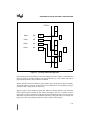

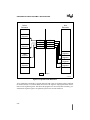

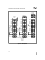


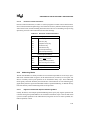

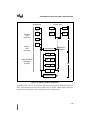

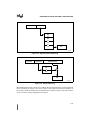

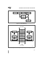
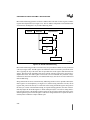
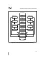


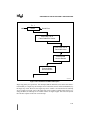
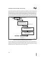
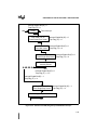


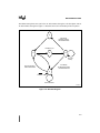

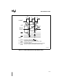
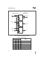

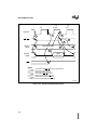


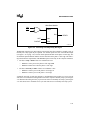
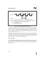
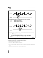
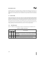


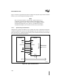


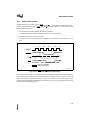

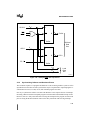

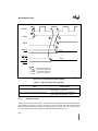


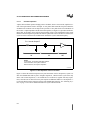


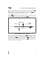

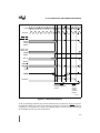

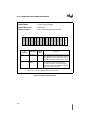
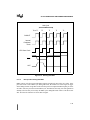

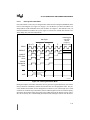

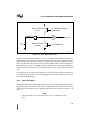

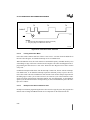


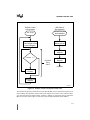


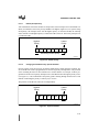
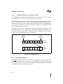


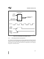
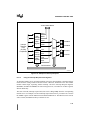
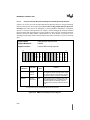

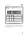


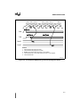
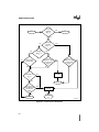
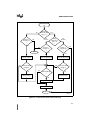


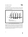


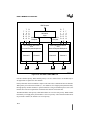


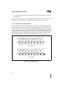
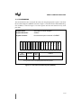

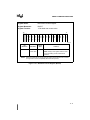

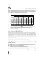


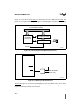

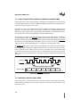


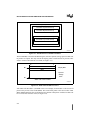
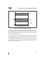
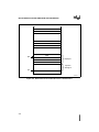
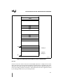


![E^YB?= ce``_bd VY\Uc V_b @QbQTYW] 4UReW BD](http://vs1.manualzilla.com/store/data/005839928_1-81490c34e940fa2480ecad1c81f1b8b0-150x150.png)