1
US006401154B1
(12) United States Patent
(10) Patent N0.:
(45) Date of Patent:
Chiu et al.
(54) FLEXIBLE ARCHITECTURE FOR AN
(75) Inventors: Kenny Kok-Hoong Chiu; Michael S.
Quimby, both of Austin, TX (US)
(73) Assignee: Advanced Micro Devices, Inc.,
Sunnyvale, CA (US)
Notice:
Jun. 4, 2002
ISA Systems Architecture, Tom Shanley & Don Anderson,
EMBEDDED INTERRUPT CONTROLLER
(*)
US 6,401,154 B1
1995, table of contents and pp. 29—37, 334—475.
82C54 CHMOS Programmable Interval Timer, Intel Cor
poration, Sep. 1993, pp. 5—24 through 5—29.
82C59A—2 CHMOS Programmable Interrupt Controller,
Intel Corporation, Oct. 1988, pp. 5—45 through 5—52.
ElanTM SC400 and Elan SC410 Single—Chip, Low—Power;
PC/AT—Compatible
Subject to any disclaimer, the term of this
patent is extended or adjusted under 35
U.S.C. 154(b) by 0 days.
Microcontrollers,
Data
Sheet,
Advanced Micro Devices, Inc., Dec. 1998, pp. 1 through
132.
ElanTM SC410 Microcontroller, Product Brief, Advanced
Micro Devices, Inc., @1999, 3 pages, http://WWW.amd.com/
products/lpd/elan410/21328a.html.
(21) Appl. No.: 09/566,205
(22) Filed:
May 5, 2000
* cited by examiner
(51)
Int. c1.7 .............................................. .. G06F 13/24
Primary Exami”@r—RuPa1 Dharia
(52)
US. Cl. ...................... .. 710/260; 710/266; 710/300
(74) Attorney) Agent» 0’ Fi’m—Ak1n> GumP’ Strauss>
(58)
Field of Search ............................... .. 710/260—266,
710/300
(56)
References Cited
4,438,492 A *
3/1984 Harmon, Jr. et al.
* 12/2000 Khan et al. ............... .. 710/107
and
E lanS C41 0
ABSTRACT
channel sWitch matrix. A scalable number of interrupt
sources can be routed to any particular interrupt request line.
In addition, from the same architecture, multiple interrupt
OTHER PUBLICATIONS
E lan TMS C400
Haw 8‘ Feld LLP
(57)
A programmable interrupt controller arrangement is pro
vided including a multiple number of selectably enabled
programmable interrupt controllers along With a multi
U.S. PATENT DOCUMENTS
6,163,826 A
_
sources are alloWed to share any one of the interrupt request
Microcontrollers
lines. Interrupt signals are routed via the sWitch matrix under
User’Manual, Advanced Micro Devices, Inc., @1997, pp.
10—1 through 10—10.
softWare control. PC/AT compatibility is achieved by selec
tively disabling certain of the programmable interrupt con
The Indispensable PC Hardware Book, Hans—Peter Messemer, Third Ed., @1997, table of contents and pp. 521—547,
“01165
659—680.
39 Claims, 8 Drawing Sheets
x/ 402
Stnrt initialization
Set interrupt trigger
x/ 404
type (edge or level)
Initialization
process
Sct cascade or
x/ 406
PC/AT mode
Cascade im'halintiun
W 41 2
Enablwdisable
interrupt enable bits
Decode
process
Enable/disable
NMI enable bits
Receive/issue
interrupt request
Routing
Trigger polarity
process
Inversion
- nine interrupt source
to interrupt priority
Channel
x/ 418
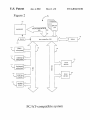
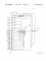
U.S. Patent
Jun. 4, 2002
Sheet 1 of 8
US 6,401,154 B1
processor address bus
J
CPU Core
@
no
processor data bus
,-----------.----
m.
P
1e
1
M.ED$2m.Ou3m
.L
B
w
P
A
8G
66
T Wbmmmr w“m."rmmcm
16%
L
I-Ul.l
w.“inr
E
Vl
mm“
m
_r
m
m
w| n.-..
1
TB
m
_
CW5
mHMS‘I0mm%IV
m
m
W.
w
.M
H
M
n
x
w
m
W
m
U
a
IsP
F
55mC&
s. 2
m
awasAulrl‘QM
mG1|v
c
Ht D
.HMM:
01c mm
“ram
InnW“3.6%
mm
nI\I-
M
smm
mm
Wm
m...“
mw
mm
M
m
mw
MW
mm
WM
Mm
m
W
mm
0mm
_
now;
nE!\b
d|
DA
m m Fm
mmI?ramIV
b
9
>
v
9+
*
+G
m.
r
r
f
K
mm
MM
E
u
m..r....
x<5mc
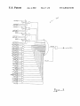
U.S. Patent
processor
Jun. 4, 2002
Sheet 2 of 8
DRAM
104
PROCESSOR BUS
0m.
m
k
H0
108
w mm
mSQv\
A
US 6,401,154 B1
w
m/6\_
msn<~
112
K
&SSmtmdmC
4Wuum5S
116
118
PC/AT-compatible system
U.S. Patent
Jun. 4, 2002
Sheet 3 of 8
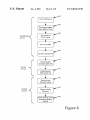
Figure 3
US 6,401,154 B1
j
I'
ISA slots
73
O
n:
V‘! ‘G’ N '- O a
65565 8 53858
118
55955595. EEEEE
\
system
IRQO
timer
112
M4\
keyboard
IRQ]
I|
interface:
_
_
_
._
._. . . _ . . .-.
_.._ .._
5° . _ . . _
I
M6
\
serial
port
_
IRQ4
IR 6
100
I
r/
> INTR
l1
V 1R1 INTR
i
l
!
!
r 1R2
r 1R3
' 1R4
1
{
!
' 1R5
E
t
g
Q
“ml
I
¢%7
7 IR6
1)
148
disk
i
controller
1'50
\
I:
parallel
IR 7
8259 PIC
i
132
E
g
:a:
r
l
INTR _
.
r
real-time
IR 12
clock
Q
1
l
1
/L—+
[R2
\
5
_/
7
!
' 1R3
l
‘—""l_> 1R4
:
, 1R5
casca e
134
.!
i
154
\.
136
IRQ
§L> 1R1
lRQ8
. \-
i
,
Port
152
“m5 er
D7:DO
!
'; , 1R6
;
I
|
l
I
r IR7
slave
‘mouse
i
mterface
i
8259 PIC
INTA# 4
Interrupt
i
Acknowledge
i
l
'56
\
numeric
coprocessor
mom
1
I
_
i
L. ........... _.I.IE§£'BEFEP.I?.SX§EEIB .......... “.5
PC/AT-compatible system
processor
U.S. Patent
Jun. 4, 2002
Sheet 5 of 8
US 6,401,154 B1
Figure 5
interrupt control register
.
blt
reset
R/W
NMI done
NMl enable
reserved
slave 2 global
slave 1 global
interrup:
interrupt
master global
interrupt
mode enable
mode enable
mode enable
0
O
0
O
O
O
R/W
W
R/W
R/w
R/W
R/W
U.S. Patent
Jun. 4, 2002
Sheet 6 of 8
CHANNEL 22 ROUTER
CHANNEL 2 ROUTER
‘
GPIRQO
p01
GPIRQIO
polarit 10
src_engl
INTA
polaritgH
INTD
QHANNEL 1 ROUTER
‘ '.
US 6,401,154 B1
U.S. Patent
Jun. 4, 2002
Sheet 7 of 8
US 6,401,154 B1
GPIRQO
olarit 0
ngliuengo
GPIRQ] 0
olarit l0
npmi_eng10
INTA
polarityl 1
nmi_enbl 1
INTD
nmi_out
_> nmi (to CPU)
m. “I.
U.S. Patent
Jun. 4, 2002
f
Sheet 8 of 8
US 6,401,154 B1
W402
Start initialization
i
Set interrupt trigger
Kl/ 404
type (edge or level)
i
Initialization
Set cascade or
process
PC/AT mode
M406
‘(1/ 408
Set vector offset
l
\
410
Cascade initialization
l
Enable/disable
412
Kl/
interrupt enable bits
Decode
l
process
Enable/disable
NMI enable bits
K’
l
‘1/414
K/ 4 l 6
Receive/issue
interrupt request
i
I
Routmg <
Trigger polarity
Process
W418
inversion
i
4
Route interrupt source [1/ 20
to interrupt priority
\
channel
Figure 8
US 6,401,154 B1
1
2
FIGS. 5A—5C are block diagrams of con?guration regis
FLEXIBLE ARCHITECTURE FOR AN
EMBEDDED INTERRUPT CONTROLLER
ters of an exemplary microcontroller according to one
embodiment;
BACKGROUND OF THE INVENTION
FIG. 6 is a detailed schematic of the interrupt router of
FIG. 4;
1. Field of the Invention
FIG. 7 is a detailed schematic of a non-maskable sWitch
This application relates to microcontroller architecture,
and more particularly to a programmable interrupt control
ler.
2. Description of the Related Art
matrix of the interrupt router of FIG. 4; and
FIG. 8 is a How diagram of an exemplary con?guration
1O
A typical interrupt controller has 8 input lines that take
DETAILED DESCRIPTION OF PREFERRED
EMBODIMENT
requests from one of 8 different devices. The controller then
passes the request on to the processor, telling it Which device
issued the request (Which interrupt number triggered the
request, from 0 to 7). The original PC and XT systems had
one of these controllers, and hence supported interrupts 0 to
The folloWing related patent applications are hereby
15
7 only.
Starting With the IBM AT, a second interrupt controller
Was added to the system to expand it; this Was part of the
expansion of the ISA system bus from 8 to 16 bits. In order
to ensure compatibility, the designers of the AT didn’t Want
incorporated by reference as if set forth in their entirety:
US. patent application Ser. No. 09/379,457, entitled
FLEXIBLE MICROCONTROLLER ARCHITECTURE;
US. patent application Ser. No. 09/379,160, entitled
BUFFER CHAINING;
US. patent application Ser. No. 09/379,015, entitled
METHOD AND APPARATUS FOR OVERLAPPING
to change the single interrupt line going to the processor. So
PROGRAMMABLE ADDRESS REGION;
US. patent application Ser. No. 09/379,012, entitled
What they did instead Was to cascade the tWo interrupt
controllers together.
The ?rst interrupt controller still has 8 inputs and a single
process.
25
GENERAL PURPOSE BUS WITH PROGRAMMABLE
output going to the processor. The second one has the same
TIMING, ?led concurrently;
design, but it takes 8 neW inputs (doubling the number of
interrupts) and output its single feed into input line 2 of the
DIRECT MEMORY ACCESS CHANNEL CONFIG
US. patent application Ser. No. 09/378,873, entitled
URABILITY SUPPORT;
US. patent application Ser. No. 09/379,020, entitled
?rst controller. If any of the inputs on the second controller
become active, the output from that controller triggers
interrupt #2 on the ?rst controller, Which then signals the
FLEXIBLE ADDRESS PROGRAMMING WITH WRAP
processor.
BLOCKING; and
US. patent application Ser. No. 09/379,019, entitled
SUMMARY OF THE INVENTION
Brie?y, the illustrative system provides an interrupt con
troller With the ?exibility to provide a PC/AT-compatible or
35
non-PC/AT-compatible embedded environment. Multiple
The microcontroller M provides a highly integrated CPU 36
slave controllers together With a master controller are com
With a complete set of peripherals that are superset of
common PC/AT peripherals and With a set of memory
bined With a multi-channel routing sWitch matrix. Flexibility
is provided through interrupt sharing and selective slave
mapped peripherals. In the disclosed exemplary
controller disabling. The sWitch matrix, under softWare
embodiment, the CPU 36 is the Am5x86 CPU core, Which
control, directs the multiple interrupt signals from internal
utiliZes the industry standard x86 microprocessor instruction
and external sources to any priority channel of the multi
stage interrupt controller. Con?guration of the sWitch matrix
may be performed upon initialiZation or during run time.
The sWitch matrix, slave controllers and master controller
cascade formation may be con?gured to utiliZe a large
45
memory and peripherals into a memory address space and an
I/O address space. The PAR registers 70 also alloW control
of important attributes like cacheability and Write protection
interrupt channels.
for memory resources. Both the PAR registers 70 and a
Con?guration Base Address register (CBAR) 78 serve as
address decode registers. While the PAR registers 70 are
memory-mapped, the CBAR 78 is direct-mapped to 1/0.
BRIEF DESCRIPTION OF THE DRAWINGS
A better understanding of the illustrative system can be
55
An address decoding unit (ADU) 38 provides ?exible
distributed memory and I/O address decode logic. Address
decode is distributed betWeen a general purpose (GP)-Bus
folloWing draWings, in Which:
FIG. 1 is a block diagram of some elements of an
exemplary microcontroller according to one embodiment;
FIG. 2 is a detailed block diagram of the circuitry of the
programmable interrupt controller of the microcontroller of
the illustrative system according to one embodiment;
FIG. 3 is a block diagram illustrating the interrupt sub
system for a typical PC/AT computer system;
FIG. 4 is a block diagram illustrating the interrupt sub
set. The CPU 36 includes an integrated 16 K Write back
cache.
The microcontroller M provides Programmable Address
Region (PAR) registers 70 that enable ?exible placement of
number of interrupt channels or alternatively, to operate
under PC/AT compatibility using a reduced number of
obtained When the folloWing detailed description of the
disclosed embodiment is considered in conjunction With the
REDIRECTING I/O ADDRESS HOLES.
Turning noW to the draWings, FIG. 1 shoWs a typical
microcontroller M in accordance With the present invention.
Controller 24, memory controllers such as a read-only
memory (ROM) controller 10 and a dynamic random access
memory (DRAM) controller 20, and a Peripheral Compo
nent Interconnect (PCI) bus 82. PC/AT-compatible periph
erals are direct-mapped to I/O, and remaining integrated
system for an exemplary microcontroller according to one
peripherals are memory-mapped. The memory space and
I/O space of a general purpose bus 72 are accessible by the
CPU 36. The memory space and I/ O space of the PCI bus 82
are accessible by the CPU 36 and PCI master controller 80,
embodiment;
and external bus masters.
65
US 6,401,154 B1
3
4
Asystem arbiter 26 includes an arbiter 66 for performing
arbitration for a processor bus 76 (shoWn divided into its
address, data, and control portions) and an arbiter 68 for
performing arbitration for the PCI Bus 82. The processor bus
arbiter 66 may arbitrate betWeen several possible processor
bus masters. For example, the processor bus arbiter 66 may
handle requests for the CPU 36, a general purpose bus
?y-by (single cycle) transfers betWeen general purpose bus
peripherals and DRAM, and variable clock modes. The
controller 22 is PC/AT-compatible.
A PIO (programmable I/O) unit 50 provides PIO logic to
support 32 programmable I/O signals (PIOs) to monitor
signals and control devices not handled by other functions of
the microcontroller M. The PIOs are shared With other
functions on the microcontroller M.
DMAC 22 and the PCI host bridge 18 on behalf of an
external bus master requesting access to DRAM. The PCI
bus arbiter 68 may arbitrate betWeen ?ve possible PCI
10
timers unit 52 include three 16-bit timers, tWo-stage cascad
masters.
ing of timers, and several modes of operations.
A processor bus interface 77 is responsible for DMA
cache snooping, dynamic clock speed adjusting, dynamic
bus siZing, ready signal consolidation. Memory Mapped
Con?guration Region (MMCR) control and general purpose
A timers unit 52 provides general purpose timers for
generic timing or counting applications. Features of the
An in-circuit emulator (ICE) core 42 provides an inte
15
address control are performed by the ADU 38. A bus
interface unit, or BIU, 34 basically assists the CPU 36 With
grated debug interface for embedded hardWare/softWare
debug during a special debug mode, ICE mode. Controlla
bility and observability may be achieved through a fast
JTAG-compliant serial interface.
APCI host bridge 18 is integrated into the microcontroller
bus, DMA, and memory control.
Aclocks module 58 provides oscillators and phase locked
loops (PLLs) to support the DRAM controller 20, UARTs
40, general purpose timers (GPT) 52, and a real-time clock
microcontroller DRAM space. The PCI Host bridge 18 may
be a 33 MHZ, 32-bit PCI Bus Revision 2.2-compliant host
(RTC) 60.
bridge interface.
M Which alloWs the CPU 36 to generate PCI master trans
actions and alloWs external PCI masters to access the
A PIC 48 includes 3 industry standard programmable
The DRAM controller 20 provides SDRAM
(synchronous DRAM) support, symmetric and asymmetri
cal DRAM support, SDRAM auto refresh support, SDRAM
interrupt controllers (PICs) integrated together With a highly
25
ering support, DRAM read pre-fetching support, read
may be programmed to operate in PC/AT-compatible mode.
around-Write support, and supports up to 256 megabytes of
DRAM. The DRAM controller 20 may service requests
from the CPU 36, the PCI host bridge 18 on behalf of an
external PCI master, or the general purpose bus DMA
controller and may issue commands to SDRAM devices.
DRAM cycles may also be initiated by a Write buffer 28 or
The router may handle routing of 33 various external and
internal interrupt sources to the 22 interrupt channels of the
three PICs.
A programmable interval timer (PIT) 62, Which is com
patible to 8254 PIT circuitry, is provided. The PIT 62
provides three 16-bit general purpose programmable
channels, six programmable counter modes, and binary and
BCD counting support.
a read-ahead buffer 30 internal to the DRAM controller 20.
The Write buffer 28 and the read-ahead buffer 30 together
provide buffering techniques to optimiZe DRAM system
performance.
The microcontroller M further includes an integrated reset
controller 44 to control the generation of soft or hard resets
to the CPU 36 and system resets to the various internal cores.
The reset controller 44 provides a control bit to enable ICE
mode after the CPU 36 has been reset.
A data steering block 12 stores data and routes data as
needed from 8/16-bit devices from/to the general purpose
bus 72 to/from a CPU bus. On DMASDRAM reads, the data
steering block 12 may save data until the next address
strobe.
An integrated ROM/Flash controller 100 provides a glue
less interface to up to three ROMs, EPROMs, or ?ash
A general purpose bus controller 24 controls the general
purpose bus 72, an internal and external bus that connects 8
or 16-bit peripherals to the microcontroller M Without glue
programmable interrupt router. TWo of the PICs 48 may be
cascaded as slaves to a master PIC Which arbitrates interrupt
requests from various sources to the CPU 36. The PICs 48
Error Correction Code (ECC) support, DRAM Write buff
45
devices. It supports asynchronous and advanced page-mode
selects, programmable bus interface timing, “ready” signal
devices.
The RTC block 60 is compatible With the Motorola MC
146818A device used in PC/AT systems. The RTC 60
support for external devices, and support for 8/ 16-bit I/ O and
memory mapped I/O cycles. In the disclosed embodiment,
the general purpose bus 72 supports a programmable inter
rupt controller (PIC) 48, a programmable interval timer
supports binary or BCD representation of time, calendar, and
alarm, its oWn poWer pin and reset, 14 bytes of clock and
control registers, 114 bytes of general purpose RAM, three
interrupts sources, battery backup capability, and an internal
(PIT) 62, a Watchdog timer (WDT) 32, the real-time clock
(RTC) 60, the general purpose timers (GPT) 52, a softWare
timer (SWT) 64, UARTs 40, a synchronous serial interface
RTC reset signal to perform a reset at poWer-up.
logic. Features of the controller 24 include 8 external chip
(SSI) 56, programmable I/O logic 50, and PC/AT compat
ibility logic 74.
The microcontroller M includes a DMA controller 22
(general purpose bus DMAC) on the general purpose bus 72.
The controller 22 is shoWn integrated With the general
purpose bus controller 24. The DMA controller 22 is
designed to handle any DMA accesses betWeen general
55
A synchronous serial interface (SSI) 56 provides ef?cient
full-duplex and half-duplex, bi-directional communications
to peripheral devices. Other features include clock speed
programmable from 64 KHZ to 8 MHZ and multiple device
enables.
AsoftWare timer (SWT) 64 is a peripheral on the GP-Bus
72 Which provides a millisecond time base With microsec
ond resolution timing for softWare. The peripheral 64
includes a 16-bit millisecond up counter and a 10-bit mil
lisecond up counter.
A test controller block 46 includes test logic such as the
Features of the controller 22 includes support for up to 7
DMA request channels (With a maximum of 4 external 65 J TAG controller. The test logic is provided to test and ensure
purpose bus peripherals (internal or external) and DRAM.
requests), support for three 16-bit channels and four 8-bit
that the components of the microcontroller M function
channels, buffer chaining capability in enhanced mode,
correctly.
US 6,401,154 B1
6
5
A UART block 40 includes tWo PC16550-compatible
Accordingly, the ISA bus 122 is a standard component of all
PC/AT-compatible systems. The ISA bus 122 has several
features, many of Which are discussed beloW. A general
function of the ISA bus 122 is to provide a mechanism for
8- or 16-bit devices to be added to the computer system S
such that the devices may interact With its other circuitry.
For example, an external device may need to interrupt the
processor 100. Accordingly, the device needs to interact With
the interrupt subsystem 112. Adherence to ISA bus 122
UARTs, both capable of running 16450 and 16550 software.
The UART block 40 supports DMA operation, a FIFO mode,
an internal baud rate clock to handle baud rates up to 1.5M
bits/s, false start bit detection, break detection, full-duplex
operation, and other features.
A Watchdog timer block (WDT) 32 is a mechanism to
alloW system softWare to regain control of the microcon
troller M When the softWare fails to behave as expected. The
Watchdog timer block 32 supports up to a 30-second time
10
requirements makes such interaction possible. FIG. 2 shoWs
a 16-bit device 126 and an 8-bit device 128 connected to the
ISA bus 122. These devices may be either soldered on the
system board or they may be connected via an ISA expan
sion slot connector. An example of an 8-bit device is a ?oppy
peripherals include the DMA controller 22, the PIT 62, the
15 disk drive controller While a ?xed disk drive controller is a
PIC 48, the UARTs 40, and the RTC 60.
out With a 33 MHZ CPU clock.
The PC/AT compatibility logic 74 provides PC/AT
compatible functions. The PC/AT compatible integrated
commonly used 16-bit device. Both are typically found in
This particular microcontroller is illustrative. The tech
niques and circuitry according to the invention could be
PC/AT systems.
The folloWing sections describe particular requirements
and implementations for PC/AT compatibility of the micro
controller M. For simplicity and clarity, requirements Which
applied to a Wide variety of microcontrollers and other
similar environments. The term “microcontroller” itself has
differing de?nitions in industry. Some companies refer to a
processor core With additional features (such as I/O) as a
are common across most computer system architectures are
“microprocessor” if it has no onboard memory, and digital
signal processors (DSPs) are noW used for both special and
general purpose controller functions. As here used, the term
“microcontroller” covers all of the products, and generally
means an execution unit With added functionality all imple
mented on a single monolithic integrated circuit.
not described herein. Thus, for example, no mention is made
of chip select signals, except Where pertinent to discussing
particular architectural requirements of a PC/AT-compatible
system.
Programmable Interrupt Controller (PIC)
PC/AT Compatibility Requirements
Before discussing the PC/AT-compatible features of the
microcontroller M of FIG. 1, a brief introduction to PC/AT
compatibility is provided. FIG. 2 is a block diagram of a
computer system S used to illustrate some of the basic
hardWare features of a PC/AT-compatible computer. First, a
processor 100, also knoWn as a microprocessor, is shoWn.
PC/AT-compatible systems are based upon the Intel 8088 or
In the PC/AT World, all hardWare interrupts to a processor
are channeled through tWo interrupt controllers. The inter
rupt controllers are Intel 8259A or their equivalent devices.
The PC/AT architecture supports tWo cascaded 8259A PICs
for a total of ?fteen maskable interrupt request sources. The
interrupt controllers are eight-input devices that can accept
compatible microprocessors. The 8086, 80286, 80386,
interrupt signals from several devices, assign priorities to
each interrupt, and then interrupt the processor. Upon receipt
80486, and Pentium microprocessors are all considered
PC/AT-compatible With the 8088 microprocessor.
of the interrupt, the processor automatically reads the par
FIG. 2 also shoWs a processor bus 102. The processor bus
102 connects the processor 100 to the other components of
ticular interrupt controller to determine the source of the
highest priority interrupt. Once determined, the processor
calls the appropriate softWare interrupt routine.
the computer system S and provides a pathWay for address,
data, and control signals to traverse. Also shoWn coupled to
the processor bus 102 is a memory or DRAM 104. The
TWo interrupt controllers, a master and a slave, are used
so that ?fteen levels of interrupts are available. The INTR
DRAM 104 contains data such as, for example, instructions
output of the slave is connected to the IR2 input of the
that the processor 100 executes.
45 master. This con?guration enables the slave interrupt con
troller to interrupt the master interrupt controller to cause an
Next, a bus controller 106 coupled to the processor bus
interrupt. Although not required, typical PC/AT systems
implement additional logic to alloW programmable steering
of the IRQs. The programmable interrupt controllers provide
102 is shoWn. The bus controller 106 contains logic Which
enables the processor 100 to communicate With external
devices. A ROM device 108 is shoWn coupled to the bus
controller 106. The ROM 108 contains ?rmWare instructions
Which are executed by the processor 100 When the computer
other features Which are Well-knoWn to PC/AT system
designers.
system S is poWered up.
A clock 124 is also shoWn as input to both the processor
100 and the bus controller 106. The clock 124 enables
synchroniZation of these and other devices so that the
processor 100 can communicate With other devices in the
FIG. 3 is a block diagram illustrating the interrupt sub
system 112 for the PC/AT-compatible system introduced in
FIG. 2. The interrupt subsystem 112 consists of tWo interrupt
55
computer system S.
of resources in the system S. The eight interrupts coming in
from the slave PIC 132 produce a single INTR signal Which
FIG. 2 shoWs tWo peripheral buses, an X bus 120 and an
ISA bus 122. The X bus 120 is simply a buffered version of
in this case goes to the IR2 line of the master PIC 130, as
the ISA bus 122. As shoWn in FIG. 2, several components of
PC/AT-compatible systems are connected to the system
through the X bus 120. These components include a DMA
subsystem 110, an interrupt subsystem 112, a keyboard
subsystem 114, a real-time clock and CMOS RAM sub
system 116, and system timers 118.
Also shoWn as part of the computer system S is an ISAbus
122. ISA is an acronym for Industry Standard Architecture.
controllers: a master PIC 130 and a slave PIC 132. Together,
the tWo PICs 130 and 132 receive interrupts from a variety
65
FIG. 3 shoWs. In a PC/AT-compatible system, the interrupt
priorities are assigned in ascending order. That is, IRO has a
higher priority than IR1 and IR2, and so on. Because the
eight interrupts from the slave PIC 132 interrupt the IR2 line
of the master PIC 130, all eight of the slave interrupts have
higher priority than IR3 through IR7 of the master PIC 130.
As FIG. 3 shoWs, the interrupt inputs are labeled IRQO
through IRQ15, for a total of sixteen interrupts for the tWo
US 6,401,154 B1
8
7
The interrupt router 168 may receive interrupts from
PICs 130 and 132. However, the INTR output from the slave
PIC 132 is an input to IR2 of the master PIC 130. Therefore,
only ?fteen IRQ interrupts are available. In PC/AT
compatible systems, the ?fteen available interrupts are
either sources external to the microcontroller M or those
internal to the microcontroller M. The external sources
include devices connected to the PCI bus 82 or the general
purpose bus 72. Additionally, the interrupt router 168 may
receive interrupts from internal sources including the ICE
42, the address decode unit 38, the programmable interval
timers 62, the UARTs 40, the real-time clock 60, the
assigned to particular logic of the computer system S.
In PC/AT-compatible systems, the IRQO is received from
a system timer 118, as FIG. 3 shoWs. IRQl is provided by
a keyboard interface 144. IRQ2 is cascaded from the slave
controller 132. IRQ3 and IRQ4 are each assigned to a serial
Watchdog timer 32, the synchronous serial interface 56, the
DRAM controller 20, the PCI host bridge 18, and the general
port in PC/AT-compatible systems. In FIG. 3, hoWever, the
purpose DMA controller 22.
The interrupt router 168 is implemented in hardWare as
combinatorial logic and is used to route any of the interrupt
IRQ3 and IRQ4 inputs are shoWn tied to ISA slots 140. The
ISA slots 140 permit one or more external serial cards to be
connected to the computer system S. The serial card(s) may
then be assigned the IRQ3 or IRQ4 inputs to the master
interrupt controller 130, as desired. The IRQ4 input is also
shoWn connected to a serial port 146. An integrated serial
port 146 is generally a part of a PC/AT-compatible system.
Next, the IRQ5 input is received from the ISA slots 140.
IRQ5 is reserved in PC/AT-compatible systems for connec
tion to a parallel port. The IRQ6 input is received from a
sources (both internally generated or externally generated),
15
the interrupt priority channels for arbitration. Signal intr Will
be presented to the processor 36 from the master PIC 160 as
an interrupt request. FIG. 6 shoWs the logical implementa
tion of the sWitch channel matrix or router 168 Which
?oppy disk controller 148. Like IRQ4, the IRQ6 input is also
connected to the ISA slots 140, alloWing for an external
?oppy disk controller to be connected to the computer
system S as desired. The IRQ7 input is from a parallel port
150. Again, the IRQ7 line is also connected to the ISA slots
consists of logically ORing, represented by the scalable OR
25
140 for expandable options.
The next eight interrupts, IRQ8 through IRQ15 are inputs
gate 254, all the interrupt sources possible for each of the 22
channels.
The interrupt vector to the processor 36, not shoWn in
FIG. 4, is transmitted through the general purpose bus 72
connecting the peripherals to the processor 36. Signal irq
[22:1]itrig are the internally generated hardWare interrupts
to the slave PIC controller 132. First, the IRQ8 input is
received from a real-time clock 152. IRQs 9, 10, 11, 14 and
15 are all shoWn coming in from the ISA slots 140. These
from interrupt trigger bits. Each channel has its oWn inter
rupt trigger bit. Another embodiment Would provide a
reduced number of internally generated hardWare interrupt
interrupts can be coupled to any 8- or 16-bit ISA devices.
In PC/AT-compatible systems, the IRQ12 input is
received from a mouse interface 154 While the IRQ13 input
is received from a numeric co-processor 156. Thus, FIG. 3
is an illustrative representation of hoW the ?fteen available
to the individual interrupt priority channels P1—P22 under
softWare control. Once routed, the interrupt sources are
output from the interrupt router 168 as irqip1—irqip22 to
35
bits (instead of one per channel) that could be used to route
to the interrupt priority channels. One skilled in the art can
understand that this architecture is not limited to the shoWn
number of interrupt sources.
From FIG. 6, each internally generated hardWare interrupt
interrupts into both the master and slave interrupt controllers
130 and 132 are organiZed in PC/AT-compatible systems.
source has its oWn enable bit, Which can be cleared through
softWare to gate the interrupt at the polarity inversion logic
Exemplary Implementation
250 or the AND gate array 252 from causing an interrupt
The microcontroller M of the illustrative system provides
a highly programmable architecture Which grants its cus
tomers the option to enable PC/AT functionality. The micro
request output over the irqip1—irqip22 output signal lines.
Also, this architecture alloWs sharing of interrupt sources
With respect to a particular interrupt channel. The OR gate
controller M provides three 8259A programmable interrupt
254 associated With each of the 22 channel routers 201—222,
controllers. The PICs for the microcontroller M can be
collectively a crossbar sWitch, alloW sharing by mapping
con?gured as either a stand-alone master controller, one 45 multiple interrupt sources to the interrupt channels. Sharing
slave cascade, or cascading With both slave controllers. The
is one manner that alloWs routing of more interrupt sources
?exible architecture thus provides embedded system design
than available interrupt priority channels. Level sensitive
ers the ability to utiliZe the tWenty-tWo interrupts available
using the three 8259A PICs, to program tWo of the PICs for
PC/AT functionality, or to disable both slaves, leaving only
eight available interrupts, as desired.
FIG. 4 is a block diagram of the programmable interrupt
controller 48 introduced in FIG. 1 as part of the microcon
troller M. The PIC 48 consists of three industry standard
sharing is typically implemented by tying multiple interrupt
programmable interrupt controllers integrated together With
outputs using an open drain or open collector output to a
single interrupt input pin. HoWever, interrupt sharing may be
easily con?gured, according to the present embodiment, by
the aforementioned mapping scheme illustrated in FIG. 6.
Interrupt sharing is preferred for level sensitive interrupts
and not edge-triggered interrupts. Edge triggered interrupts
55
are not recommended to be shared because it is dif?cult to
a highly programmable interrupt router. Accordingly, FIG. 4
keep track of the number of edges being generated to signify
shoWs a master PIC 160, a slave PIC 162, a second slave PIC
164, and an interrupt router or channel sWitch matrix 168.
The tWo industry standard PICs 162 and 164 are cascaded as
slaves to the master PIC 160. The master PIC 160 arbitrates
interrupt requests. Furthermore, glitches Which can occur so
frequently on these lines (due to asynchronous nature of
most PC interrupt controllers) are difficult to differentiate
With real interrupt signals. Level sensitive interrupts can be
interrupt requests from various sources to the CPU 36. The
shared as the interrupt remains active before the end-of
programmable interrupt router 168 handles routing of the
interrupt is performed and thus is easily recogniZable. In
edge triggered interrupts, this information is lost.
Returning to FIG. 5, the interrupt control register 167
controls the global interrupt mode (edge vs. level) for the
various external and internal interrupt sources to the tWenty
tWo interrupt channels of the three PICs 160, 162 and 164.
Speci?cally, the PIC 48 is able to handle more interrupt
sources than available interrupt priority channels.
Interrupt Router/SWitch Matrix
65
master 160, slave 1 162 and slave 2 164 programmable
interrupt controllers. According to an embodiment, bits [2:0]
US 6,401,154 B1
9
10
control the global interrupt mode for each of the PICs. Each
bit, along With the respective LTIM bit of PICICW1 register
the NMI sWitch matrix 300. NMI sharing is possible With
this architecture but is preferred for level sensitive NMI
for the same PIC (see FIG. 5B), provides a global or
individual channel interrupt mode for the respective PIC is
requests.
The polarity control signal per external interrupt source is
set. If this bit is set and the LTIM bit cleared, all the PIC
common to those used across the channel sWitch matrices.
The NMI enable bits for each source are enabled/disabled
interrupt channels Will recogniZe edge sensitive interrupt
requests. If this bit is cleared, hoWever, the PIC channels can
be programmed individually to select either edge or level
under softWare control.
PC/AT Compatibility
sensitive interrupt recognition. Bit 2 of this register controls
slave 2 PIC global interrupt mode enable. Bit location [1]
controls PIC global interrupt mode enable for slave 1 and bit
location [0] controls the PIC global interrupt mode enable
The PIC 48 of the microcontroller M is designed to
support PC/AT compatibility. In this respect, the program
mable interrupt router 168 may be con?gured at startup or
during normal operation to appropriately route ISA interrupt
signals to the corresponding interrupt channels of the slave
for the master PIC. According to one embodiment, for
PC/AT compatibility, bits [1:0] should set together With bits
S2(set) and S5(cleared) of register PIC ICW3 (see FIG. 5C).
In such a case, slave 2 controllers bypass any interrupt
15
sources mapped to slave 2 controller and should have no
PICs 162 and 164 and the master PIC 160. Table 1 beloW
shoWs the interrupt channel assignment for PC/AT
compatible systems and the corresponding interrupt of the
effect.
microcontroller M. These channel assignments are imple
Externally generated interrupts e.g. INTA—INTD and
GPIRQO—GPIRQ10 go through the polarity inversion logic
mented in softWare, typically during BIOS initialiZation.
250 to further provide ?exibility in the architecture to
accommodate different types of interrupt sources. For
example, a PCI generated interrupt request that is active loW
must be inverted using this programmable inversion logic
250 prior to reaching the interrupt priority channel to Which
TABLE 1
PC/AT interrupt channel assignment for the microcontroller M
25 No.
it is mapped before the controller can recogniZe a valid
interrupt request. All internally-generated interrupt signals
may have the correct active high polarity and therefore do
not require inversion. Although this embodiment is
described in connection With the cascaded interrupt control
ler architecture, it should be understood this same concept
may be extended With only minor modi?cation to any
interrupt controllers that recogniZe either ?xed active (high
or loW) interrupt requests or ?xed edge-triggered (loW-to
high or high-to-loW) interrupt requests.
I/O device
microcontroller M interrupt source
IRQO
System Timer( )
Internal via pitiOiirq
IRQ1
Keyboard Interface
External via General Purpose IRQ
pin
IRQZ
IRQ3
IRQ4
IRQ5
Slave1 cascading
Serial Port 2
Serial Port 1
Parallel Port 2
IRQ6
Floppy Disk Controller
Cascaded from Slave Controller
Internal via uartZiirq
Internal via uartliirq
External via General Purpose IRQ
pin
External via General Purpose IRQ
pin
IRQ7
Parallel Port 2
External via General Purpose IRQ
pin
35
It should also be understood that the architecture is easily
scalable to accommodate more than the number of interrupt
IRQ8
IRQ9
Real Time Clock
Internal via rtciirq
Any 8 or 16 bit ISA device External via General Purpose IRQ
sources shoWn simply by Widening the channel sWitch
IRQ1O
Any 8 or 16 bit ISA device External via General Purpose IRQ
routed through a simple OR device, additional interrupt
IRQ11
Any 8 or 16 bit ISA device External via General Purpose IRQ
sources can be added Without signi?cant changes in the
hardWare design. A modi?cation to the AND gate array 252
IRQ12
Mouse Interface
(FIG. 6) and, if an active loW interrupt is used, a modi?ca
tion to the polarity inversion array 250 could easily be made
IRQ13
Numeric Co-processor
IRQ14
Any 8- or 16-bit ISA device External via General Purpose IRQ
to accommodate additional sources. Also, softWare control 45
IRQ15
can easily be modi?ed to gate the additional sources.
Any 8- or 16-bit ISA device External via General Purpose IRQ
pin
matrix 168. Speci?cally, since the interrupt sources are
pin
pin
External via General Purpose IRQ
pin
In FIG. 6, all of the thirty-tWo hardWare interrupt sources
Internal via ferriirq
pin
pin
are common to all the tWenty-tWo channel routers 201—222.
Returning to FIG. 4, a multiplexor 170 and 172 is imple
The individual bits of polarity [14:0] per external interrupt
source is also common to all the channel routers 201—222.
mented at the output of each slave controller 162 and 164 to
The decoder for the enable signals is not shoWn; only the
decoded representation of the signals is shoWn. Those
provide PC/AT compatibility. When signals s2 and s5,
skilled in the art are generally familiar With the design of
decoders When given an encoder design. Each channel
crossbar sWitch matrix 201—222 has its oWn unique inter
cleared respectively under softWare control, PC/AT compat
ibility could be maintained Whereby the outputs of slave 1
control signals for the multiplexors 170 and 172, are set and
nally generated hardWare interrupt trigger irq[1]itrig—irq
controller is cascaded onto IR2 input of master controller
respectively and slave 2 controller is disabled. Different
[22]itrig.
master and slave(s) con?gurations could be programmed
Turning to FIG. 7, there is also a non-maskable interrupt
(NMI) sWitch matrix 300 for all the interrupt sources. Signal
depending on the signals s2 and s5.
Additional embodiments exist to provide further ?exibil
ity. One alternate embodiment is to provide another level of
sWitch matrix betWeen the slave controllers 170 and 172 and
the master controller 160. This alloWs routing the output of
each slave to any input of the master controller under
softWare control. This additional sWitch matrix Would be
55
nmiitrig is an internally generated NMI trigger bit Which
can be used to generate an NMI under softWare control. FIG.
7 shoWs the logical OR function of this sWitch matrix,
similar to the channel routers 201—222. Signal nmi is pre
conditioned to be synchronous to the processor clock before
being presented to the processor 36 and the circuit is not
shoWn. Similarly, this architecture can be scaled to accom
modate more NMI sources than What is shoWn by Widening
65
implemented in much the same Way as the interrupt router
168. Speci?cally, through minimal additional softWare
control, additional interrupt trigger bits associated With the
US 6,401,154 B1
11
12
priority interrupt signals output from the slave controllers
simplicity, the discussion of the registers of FIGS. 5B and
5C will discuss only bit locations of primary importance to
the subject matter herein. Bit location [3] sets the level
triggered interrupt mode. If bit [3] is set to Zero, edge
sensitive interrupt detection is enabled and if set to 1, level
sensitive interrupt detection is enabled. Bit location [1],
SNGL sets the single PIC mode. Speci?cally, set to 0, the
system is con?gured in a cascade mode, while if set to 1,
only a single PIC system is enabled. Setting this bit to 1 then
170 and 172 could be used to route certain interrupt sources
from the slave controllers to any selected input to the master
controller. Software control would continue to maintain
PC/AT compatibility by ensuring the PC/AT priority
scheme. Another embodiment would require additional
hardware i.e. increased additional slave controllers which
would effectively increase priority interrupt channels to the
entire system up to a maximum of 64 priority interrupt
channels by using 8 slave controllers cascaded onto master
controller. This would allow systems to take advantage of a
signi?cant increase the number of interrupt sources possible.
Also shown in FIG. 4 is a set of con?guration registers
166 coupled to the interrupt router 168. The con?guration
registers 166 control the PIC 48 of the microcontroller M.
10
the master PIC. In routing the interrupt request from slave 1
and slave 2 directly to IR2 and IRS of the master PIC
15
The con?guration registers 166 include both memory
mapped and direct-mapped registers. The memory-mapped
registers of the PIC 48 are mapped into the memory-mapped
con?guration register space of the microcontroller M.
mapping for both the internal peripheral sources listed above
and for eXternal sources connected to the buses 72 and 82.
25
compatible system.
FIG. 5A is a block diagram of one of the memory-mapped
registers of the microcontroller M known as an interrupt
control register 167. The bottom three bits control the global
interrupt mode enable feature for each of the master 160, the
slave 162, and the slave 164. For example, if bit 0 of the
interrupt control register 167 is set, the global interrupt mode
for the master PIC 162 is enabled. The global interrupt mode
allows the individual controller to either recogniZe the edge
or level sensitive interrupts (at its 8 inputs) either globally or
individually. For PC/AT compatibility, bits 1 and 0 of the
interrupt control register 167 are set, while bit 2 is cleared.
respectively. Continuing, the master PIC operation control
ler 2 (MPICOCW2) is the register providing control for
various interrupt priority control and end of interrupt of
modes. Bits [2:0] set the speci?c end of interrupt level select.
Binary values 000—111b select for IRQO—IRQ7 respectively.
Master PIC operation controller 3 (MPICOCW3) provides
control for IRR/ISR register reads, master and poll modes.
Master PIC initialiZation control word 2 (MPICICW2) is the
second initialiZation register of the master controller. Bit
Among other functions, these registers control the interrupt
The direct-mapped registers are accessible in the PC/AT I/O
address space of the microcontroller M. Refer to Table 2,
below, for particular I/O port assignments for a PC/AT
will logically remove slave 1 and slave 2 controllers from
35
locations [7:3] identify the base interrupt vector number. For
eXample, these bits will be programmed to 00001b for the
master PIC (IRQO generates INT8), and 01110b for the slave
PIC (IRQ8 corresponds to INT 70h) in a PC/AT compatible
system. Further, bit locations [2:0] represent bit locations
A10 through A8 of the interrupt vector. These bits are always
0 in a PC/AT compatible system.
Turning to FIG. 5C, additional con?guration registers are
shown. The master PIC initialiZation control word 3
(MPICICW3) is the third initialiZation register of the master
controller. This register controls the slave cascading con
?guration for the various interrupt channels. For each bit
location, a 0 couples the respective device to the respective
IRQ input. When bit location is set to 1, then the respective
IRQ input is used for slave cascading. If bits 2 and 5 of this
register are cleared, both slave controllers are logically
removed from the cascade chain to the master controller and
Upon power-on-reset, these bits are ‘set’ to further maintain
only 8 interrupt request priority levels are available to the
PC/AT compatibility.
user. Continuing, the master PIC initialiZation controller 4
Con?guration/InitialiZation
(MPICICW4) is the fourth initialiZation register of the
master controller. InitialiZation of this register is optional
unless bit location [0] of register MPICICW1 is set.
The PIC 48 includes a set of con?guration registers 166,
as shown in FIG. 5. These registers include an interrupt
request register, in-service registers, interrupt mask register,
four initialiZation control words, and 2 operation control
45
words per controller.
Continuing, the master PIC interrupt mask (MPICINTMSK)
provides masking of individual interrupt request for the
master controller. A 0 value in any bit location unmasks the
respective IRQ signal. Alternatively a 1 in a bit location
The register names are:
masks the respective interrupt input.
A set of such registers is available for each controller 160,
162, and 164. Additional registers could be added to the
Master Controller
Slave Controller 1
Slave Controller 2
system with only minor modi?cation for applications
MPICICW1
MPICICWZ
MPICICW3
MPICICW4
MPICOCWZ
MPICOCW3
MPICOCW1
S1PICICW1
S1PICICW2
S1PICICW3
S1PICICW4
S1PICOCW2
S1PICOCW3
S1PICOCW1
S2PICICW1
SZPICICWZ
S2PICICW3
S2PICICW4
SZPICOCWZ
S2PICOCW3
S2PICOCW1
involving more than two slave controllers, as discussed
(also known as IntI
mask register)
55
(also known as IntI mask (also known as IntI mask
register)
correspond to the I/O port assignments required for PC/AT
register)
compatibility.
The initialiZation of the PIC 48 consists of writing a
sequence of two to four bytes to each of the master PIC 160,
the slave PIC 162, and the slave PIC 164. The ?rst initial
FIGS. 5B and 5C illustrate the various con?guration
registers of an embodiment. These will be described in the
conteXt of the master controller. Minor differences eXist for
analogous slave controller registers. Turning speci?cally to
FIG. 5B shown are 4 of the 7 con?guration registers. The
master PIC initialiZation control word 1 (MPICICW1) is the
?rst initialiZation register of the master controller. For
above. These are direct-mapped registers assigned to I/O
ports 20h—21h for the master PIC 160, 24h—25h for the slave
PIC 164, and 0A0h—0A1h for the slave PIC 162 of the
microcontroller M. The I/O port assignments for the master
PIC 160 and the slave PIC 162 for the microcontroller M
65
iZation byte is written to the lower address of each interrupt
controller (020h for the master 160, OAOh for the slave 164,
and 024h for the slave 162). All subsequent initialiZation
bytes are written to the upper address of the interrupt
controllers (021h for the master 160, 0A1h for the slave 164,
US 6,401,154 B1
14
13
For PC/AT compatibility, any interrupt sources used in the
and 025h for the slave 162). Hardware programmers of
ordinary skill Will recognize this programming sequence as
system must be mapped to the appropriate interrupt priori
ties outlined in table 1 via the interrupt mapping registers
preferred for 8259 and 8259-compatible interrupt control
lers.
residing in CONFIG REGISTERS 166 of FIG. 4.
In addition to the registers shoWn in Table 2, an interrupt
control register 167 of FIG. 5, one of the many memory
TABLE 2
mapped registers of the microcontroller M, is programmed
for PC/AT compatibility by setting bits 1 and 0 of the
register. These bits provide control for global or individual
Con?guring the PIC 48 of the microcontroller M
PC/AT-compatible
in general
system
for master 160, slave
162, and slave 164:
for master 160 and
slave 162:
1.
ICW1[1] = Ob
initialize ICW1
PC/AT programming
example
20h = 15h
AOh = 15h
2.
3.
initialize ICW2 With master
vector offset value
slave
initialize ICW3 if
Master
ICW1 Was set for
cascaded PICs
ICW2 = 08h
ICW2 = 70h
ICW3[2] =
1b
channel interrupt mode control for each of the controllers.
For PC/AT compatibility, all the 8 channels are controlled
globally to either recognizing level sensitive or edge sensi
tive interrupts on all its input. These bits default to ‘set’ upon
(master 160 uses I/O
20h and 21h slave 162
uses I/O AOh and A1h)
21h = 08h
A1h = 70h
21h = 04h
A1h = 02h
15
Thus, the PIC 48 of the microcontroller M alloWs embed
ded system designers to program the PIC 48 for PC/AT
compatibility. In this case, only one of the slave controllers
is cascaded to the master controller 160 via input IR2. The
second slave controller is logically removed from the master
ICW3[5] =
Ob
Slave
4.
ICW3 = 02h
initialize ICW4 only ICW4[1] = Ob
if ICW1 provides
ICW4[4] = Ob
21h = 01h
A1h = 01h
controller 160 and the highest priority channel originally
hooked to the second controller is noW automatically routed
for
to input IR5 of the master controller 160, thereby preserving
the architecture of the PC/AT interrupt controller.
Table 2 shoWs hoW the PIC 48 of the microcontroller M
may be con?gured for either a PC/AT-compatible system or
for a non-PC/AT-compatible system. Up to four initialization
Alternatively, embedded system designers may fully utilize
the tWenty-tWo available interrupts of the PIC 48 for other
applications, as desired.
The programmable interrupt controller consists of a sys
control Words, denoted ICW1, ICW2, ICW3, and ICW4,
may be programmed for each of the master controller 160,
the slave controller 162, and the second slave controller 164.
An optional 3 operation control Words can also be pro
grammed after the four initialization control Words are
performed for each controller to further con?gure the con
trollers.
First, the ICW1 register is initialized. This initialization
poWer-on-reset Which maintains PC/AT compatibility, for
example the register of FIG. 5.
tem of three individual interrupt controllers (Master, Slave 1
and Slave 2), each of Which has eight interrupt channels. The
interrupt controller is implemented asynchronously. TWo of
the interrupt channels on the Master controller are used to
cascade the slave controllers. This alloWs a total of 22
35
byte noti?es the relevant PIC (master 160, slave 162, or
slave 164) that an initialization sequence is commencing.
The ICW1 register also controls the type of interrupt trig
gering (edge- or level-sensitive), Whether or not the relevant
interrupt priority levels in the ElanSC520 microcontroller.
The priority levels are numbered from P1—P22 to indicate
Which priority levels are assigned to slave or master
controllers, With P1 being the highest and P22 being the
loWest priority.
PIC 160, 162, or 164 is in a cascaded environment or alone,
Turning noW to FIG. 8, shoWn is an example of an
and Whether the fourth initialization control Word (ICW4) is
interrupt ?oW sequence through the PIC 48. The initializa
tion process begins at step 402 upon initial con?guration.
HoWever, it should be understood that the programmable
nature of the components involved, including the interrupt
required. For PC/AT-compatible interrupt control, bit 1 of
the ICW1 is set to a zero. Accordingly, the third column of
Table 2 shoWs programming examples for programming the
ICW1 register for both the master 160 and one slave 162.
45
tains the vector offset for the relevant PIC 160, 162 or 164.
For PC/AT-compatible systems, the ICW2 register for the
above, this provides ?exibility in alloWing compatibility
master PIC 160 contains an 08h While the ICW2 register for
the slave PIC 162 contains a 70h, as Table 2 shoWs. Third,
With any number of various interrupt sources. At step 406,
PC/AT mode can be enabled under softWare control by
the ICW3 register is initialized. The ICW3 register is
initialized only if the ICW1 register Was programmed to
setting a particular cascade mode con?guration. PC/AT
compatibility generally requires that only one of the multiple
cascade one or more interrupt controllers. Programming the
ICW3 register identi?es Which IR inputs of the master PIC
160 are hooked up to the slave PICs 162 and 164. Looking
back to FIG. 4, the slave PIC 162 is input to the master PIC
160 at IR2. The slave PIC 164 is input to the master PIC 160
at IR5. Thus, in a PC/AT-compatible implementation of the
microcontroller M, bit 2 of the ICW3 register is set While bit
5 of the ICW3 register is cleared, since a single slave PIC
162 is sufficient for PC/AT compatibility.
Next, Table 2 shoWs that the ICW4 register is initialized.
router 168, as Well as the slave and master PICs 162, 164 and
160, alloW for run-time programming of the interrupt rout
ing process. Continuing at step 404, either edge-sensitive or
level-sensitive interrupt trigger type is set. As discussed
Next, the ICW2 register is initialized. This register con
55
slave PIC devices be enabled. Continuing, softWare may
then set the vector offset at step 408. If set at step 406, the
particular cascade con?guration is then initialized at step
410. Of course, the particular initialization process herein
described, may be performed through sequences other than
that described in connection With FIG. 8.
Continuing, at step 412, the active interrupt sources are
mapped to proper interrupt priority channel. At step 414,
necessary polarity inversion con?guration is programmed
The ICW4 register con?gures the relevant PIC for special
fully nested mode, buffered mode, automatic end of interrupt
mode, and microprocessor mode. An optional 30CW regis
for certain active loW requests input. The decoding process
ters can be programmed to further con?gure the P1 control
lers.
rupt signals are set to activate a particular internet source on
continues to step 416 Where the various enable bits and
associated enable signals including the non-maskable inter
a per channel router 201—222 basis. At step 418, certain of
US 6,401,154 B1
15
16
the interrupt priority channels are unmasked. This is done
via the interrupt mask register in the individual master and
slave controllers. Finally at step 420, the channel router is
ready to receive a issued interrupt request.
a logic circuit to direct enabled interrupt signals to the
interrupt request line associated With the channel
router.
5. The interrupt routing device of claim 4, Wherein the
interrupt signals are enabled according to predetermined
values of interrupt trigger bits associated With each interrupt
Asynchronous Operation
It can be noted that this architecture lends itself Well to
asynchronous interrupt controllers since the combinatorial
logic of the sWitch matrix Will very likely generate glitches
signal.
Whenever there are interrupts active on the interrupt priority
values of the interrupt trigger bits are set under softWare
control.
7. The interrupt routing device of claim 2, further com
channels. This is acceptable since the interrupt controllers
themselves are designed With accepting asynchronous inter
6. The interrupt routing device of claim 4, Wherein the
10
rupts Which can be glitchy. There is no special hardWare
prising:
needed to pre-condition the interrupt signals feeding into the
controllers. The enable bit for each interrupt source can be
used to test the connectivity of the interrupt source to the
priority channel at the system level. This applies to the NMI
sWitch matrix as Well. HoWever, preconditioning of the NMI
occurs synchronously before feeding into NMI pin of CPU
because a timing requirements of CPU according to US.
patent application Ser. No. 09/518,489, entitled MICRO
a router betWeen the plurality of slave interrupt controllers
15
lines from any of the plurality of slave interrupt con
trollers to any input of the master interrupt controller.
8. The interrupt routing device of claim 4, the plurality of
channel routers further comprising:
a polarity inversion circuit coupled to a selected plurality
of channel router inputs of the plurality of channel
CONTROLLER INCLUDING A CPU HAVING EDGE
SENSITIVE NON-MASKABLE INTERRUPT (NMI) CIR
routers for inverting interrupt signals.
CUITRY AND AN INTERRUPT CONTROL UNIT
9. The interrupt routing device of claim 1, further com
PROVIDING FOR NMI SHARING, herein incorporated by
reference.
The foregoing disclosure and description of the various
embodiments are illustrative and explanatory thereof, and
various changes in the descriptions of the microcontroller
and other circuitry, the organiZation of the components, and
25
sor.
a master programmable interrupt controller and a slave
programmable interrupt controller of the plurality of pro
grammable interrupt controllers are enabled in a PC/AT
compatible mode.
11. The interrupt routing device of claim 1, Wherein the
35
plurality of interrupt sources to a plurality of interrupt
of programmable interrupt controllers comprising:
a master programmable interrupt controller and ?rst slave
programmable interrupt controller enabled in the
PC/AT-compatible mode and a non-PC/AT-compatible
mode; and
lines, a ?rst set of programmable interrupt controllers
of the plurality of programmable interrupt controllers
being disabled in a PC/AT-compatible mode and a
second set of programmable interrupt controllers of the
a second slave programmable interrupt controller disabled
in the PC/AT-compatible mode and enabled in the
plurality of programmable interrupt controllers being
45
2. The interrupt routing device of claim 1, Wherein the
plurality of programmable interrupt controllers include a
plurality of slave interrupt controllers for selecting among
the interrupt request lines according to a prede?ned interrupt
signal priority and a master interrupt controller for selecting
among the selected interrupt request lines received from the
plurality of slave interrupt controllers.
3. The interrupt routing device of claim 2, further com
and non-maskable interrupt sources on a single interrupt
priority channel.
14. The interrupt routing device of claim 13, Wherein the
number of interrupt sources is more than the available
number of interrupt priority channels.
15. The interrupt routing device of claim 13, Whereby
55
PC/AT-compatible mode.
4. The interrupt routing device of claim 1, the program
mable router further comprising:
a plurality of channel routers to route one of the plurality
of interrupt signals to an interrupt request line associ
ated With a channel router of the plurality of channel
gered or level triggered on a per interrupt source basis.
routers, thereby forming an interrupt sWitch matrix,
and
interrupt sharing is provided for both internally generated
interrupts and externally generated interrupts.
16. The interrupt routing device of claim 1, Wherein the
plurality of interrupt sources are recogniZed as edge trig
gered in a edge triggered interrupt mode or as level triggered
in a level triggered interrupt mode.
17. The interrupt routing device of claim 16, Wherein the
interrupt mode is selectable such that all of the interrupts are
recogniZed as either edge triggered or level triggered in a
global mode or individually recogniZed as either edge trig
disable programmable interrupt controllers of the plu
rality of programmable interrupt controllers in a
a selection circuit to selectably enable interrupt signals;
non-PC/AT-compatible mode.
13. The interrupt routing device of claim 1, Wherein the
programmable router provides for sharing of the interrupt
prising:
comprising:
plurality of programmable interrupt controllers comprise
8259-compatible programmable interrupt controllers.
12. The interrupt routing device of claim 1, the plurality
request lines;
a plurality of programmable interrupt controllers coupled
to the programmable router by the interrupt request
an interrupt control register to selectively enable and
a non-maskable interrupt channel router to route one of a
10. The interrupt routing device of claim 1, Wherein only
1. An interrupt routing device, comprising:
enabled in a non-PC/AT-compatible mode.
prising:
plurality of non-maskable interrupt signals to a proces
the order and timing of steps taken, as Well as in the details
of the illustrated system may be made Without departing
from the spirit of the invention.
What is claimed is:
a programmable router to route interrupt signals from a
and the master interrupt controller, the second interrupt
sWitch matrix directing any of the interrupt request
65
18. A method of con?guring a programmable interrupt
controller, the method comprising the steps of:
enabling a master programmable interrupt controller;
US 6,401,154 B1
17
18
a selection circuit to selectably enable individual inter
selectively enabling none, one or more slave program
rupt signals; and
mable interrupt controllers of a plurality of slave pro
grammable interrupt controllers to generate a desired
a logic circuit to direct enabled interrupt signals to the
interrupt request line associated With the channel
number of interrupt channels.
19. The method of claim 18, Wherein the plurality of
interrupt sources are recognized as edge triggered in a edge
router.
27. The microcontroller of claim 26, Wherein the interrupt
signals are enables according to predetermined values of
triggered interrupt mode or as level triggered in a level
triggered interrupt mode.
interrupt trigger bits associated With each interrupt signal.
20. The method of claim 19, Wherein the interrupt mode
is selectable such that all of the interrupts are recogniZed as
either edge triggered or level triggered in a global mode or
10
29. The microcontroller of claim 26, further comprising:
individually recogniZed as either edge triggered or level
a router betWeen the plurality of slave interrupt controllers
triggered on a per interrupt source basis.
21. The method of claim 18, Wherein, for PC/AT
compatibility, the master programmable interrupt controller
15
and the master interrupt controller, the second interrupt
sWitch matrix directing any of the interrupt request
lines from any of the plurality of slave interrupt con
trollers to any output of the master interrupt controller.
30. The microcontroller of claim 26, the plurality of
channel routers further comprising:
a polarity inversion circuit coupled to a selected plurality
of channel router inputs of the plurality of channel
is enabled and one slave programmable interrupt controller
of the plurality of slave programmable interrupt controllers
is enabled or disabled.
22. The method of claim 18, Wherein for non-PC/AT
compatibility, a master programmable interrupt controller is
enabled and a combination of the other programmable
interrupt controllers are enabled.
23. A ?exible PC/AT-compatible microcontroller, com
routers for inverting interrupt signals.
31. The microcontroller of claim 23, further comprising:
prising:
an x86-compatible processor;
a processor bus coupled to the x86-compatible processor;
28. The microcontroller of claim 23, Wherein the values of
the interrupt trigger bits are set under softWare control.
25
a non-maskable interrupt channel router to route one of a
plurality of non-maskable interrupt signals to a proces
sor.
a general purpose bus;
a general purpose bus controller coupled betWeen the
processor bus and the general purpose bus, the general
32. The microcontroller of claim 23, Wherein only a
master programmable interrupt controller and a slave pro
grammable interrupt controller of the plurality of program
purpose bus controller, comprising:
mable interrupt controllers are enabled in a PC/AT
a means for con?guring the general purpose bus to
emulate an industry standard architecture
compatible mode.
33. The microcontroller of claim 23, Wherein the plurality
of programmable interrupt controllers comprise 8259
compatible bus;
a plurality of PC/AT peripheral devices;
35
a programmable router to route interrupt signals from a
plurality of interrupt sources to a plurality of inter
34. The microcontroller of claim 23, the plurality of
programmable interrupt controllers comprising:
rupt request lines; and
a plurality of programmable interrupt controllers
coupled to the programmable router by the interrupt
request lines, a ?rst set of programmable interrupt
controllers of the plurality of programmable inter
a master programmable interrupt controller and ?rst slave
programmable interrupt controller enabled in the
PC/AT-compatible mode and a non-PC/AT-compatible
mode; and
rupt controllers being disabled in a PC/AT
compatible mode and a second set of programmable
interrupt controllers of the plurality of program
compatible programmable interrupt controllers.
a second slave programmable interrupt controller disabled
in the PC/AT-compatible mode and enabled in the
45
mable interrupt controllers being enabled in a non
non-PC/AT-compatible mode.
35. The microcontroller of claim 23, Wherein the pro
PC/AT-compatible mode.
grammable router provides for sharing of the interrupt and
24. The microcontroller of claim 23, Wherein the plurality
of programmable interrupt controllers include a plurality of
slave interrupt controllers for selecting among the interrupt
request lines according to a prede?ned interrupt signal
priority and a master interrupt controller for selecting among
the selected interrupt request lines received from the plu
non-maskable interrupt sources on a single interrupt priority
channel.
36. The microcontroller of claim 35, Wherein the number
rality of slave interrupt controllers.
25. The microcontroller of claim 24, further comprising:
sharing is provided for both internally generated interrupts
and externally generated interrupts.
of interrupt sources is more than the available number of
interrupt priority channels.
37. The microcontroller of claim 36, Whereby interrupt
55
an interrupt control register to selectively enable and
38. The controller of claim 23, Wherein the plurality of
interrupt sources are recogniZed as edge triggered in a edge
triggered interrupt mode or as level triggered in a level
disable programmable interrupt controllers of the plu
rality of programmable interrupt controllers in a
PC/AT-compatible mode.
triggered interrupt mode.
26. The microcontroller of claim 23, the programmable
router further comprising:
39. The controller of claim 38, Wherein the interrupt mode
is selectable such that all of the interrupts are recogniZed as
either edge triggered or level triggered in a global mode or
a plurality of channel routers to route one of the plurality
individually recogniZed as either edge triggered or level
of interrupt signals to an interrupt request line associ
ated With a channel router of the plurality of channel
routers, thereby forming an interrupt sWitch matrix,
comprising:
triggered on a per interrupt source basis.
65
*
*
*
*
*