1
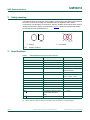
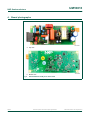
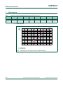
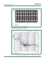
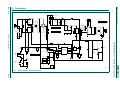
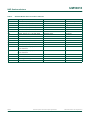
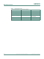
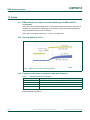
UM10813 SSL5301DB1204 120 V 36 W fixtures, isolated high PF mains dimmable LED driver demo board Rev. 1.1 — 15 October 2014 User manual Document information Info Content Keywords SSL5301DB1204, SSL5301T, flyback converter, high Power Factor (PF), high efficiency, low Total Harmonic Distortion (THD), 120 V mains, main phase-cut dimmable Abstract This document describes the operation of the SSL5301DB1204 36 W LED driver demo board featuring SSL5301T and using an isolated flyback topology. The demo board is designed for mains phase-cut dimmable applications used in Solid-State Lighting (SSL) applications. UM10813 NXP Semiconductors SSL5301DB1204 120 V 36 W LED driver demo board Revision history Rev Date Description v.1.1 20141015 updated version v.1 20140820 first issue Contact information For more information, please visit: http://www.nxp.com For sales office addresses, please send an email to: [email protected] UM10813 User manual All information provided in this document is subject to legal disclaimers. Rev. 1.1 — 15 October 2014 © NXP Semiconductors N.V. 2014. All rights reserved. 2 of 22 UM10813 NXP Semiconductors SSL5301DB1204 120 V 36 W LED driver demo board 1. Introduction WARNING Lethal voltage and fire ignition hazard The non-insulated high voltages that are present when operating this product, constitute a risk of electric shock, personal injury, death and/or ignition of fire. This product is intended for evaluation purposes only. It shall be operated in a designated test area by personnel qualified according to local requirements and labor laws to work with non-insulated mains voltages and high-voltage circuits. This product shall never be operated unattended. This user manual describes the operation of the SSL5301DB1204 36 W isolated flyback converter driver demo board featuring the SSL5301T. The demo board is designed for 120 V mains phase-cut dimmable applications. The SSL5301DB1204 demo board is designed for 48 V at a 700 mA LED string load. The single layer PCB with dimensions 120 mm 50 mm 30 mm is intended for fixtures used in SSL applications. The SSL5301DB1204 demo board provides a simple and effective solution for a 120 V mains application. It includes a high Power Factor (PF), high efficiency, and a low Total Harmonic Distortion (THD). The topology uses a single stage flyback converter without Power Factor Correction (PFC) pre-stage. 1.1 Features • SSL5301T LED driver • Single stage flyback converter without PFC pre-stage • 120 V mains phase-cut dimmable for Leading-Edge (LE), Trailing-Edge (TE) and smart dimmers • • • • • • • • • Open LED string protection Short circuit LED string protection OverCurrent Protection (OCP) OverTemperature Protection (OTP) Power factor > 0.95 THD < 10 % Efficiency > 88 % Compliant with IEC61000-3-2 harmonics standard Compliant with FCC15 EMC standard Figure 2 shows the assembled top and bottom board views. UM10813 User manual All information provided in this document is subject to legal disclaimers. Rev. 1.1 — 15 October 2014 © NXP Semiconductors N.V. 2014. All rights reserved. 3 of 22 UM10813 NXP Semiconductors SSL5301DB1204 120 V 36 W LED driver demo board 2. Safety warning The board must be connected to mains voltage. Avoid touching the demo board while it is connected to the mains voltage. An isolated housing is obligatory when used in uncontrolled, non-laboratory environments. Galvanic isolation of the mains phase using a variable transformer is always recommended. Figure 1 shows the symbols that identify the isolated and non-isolated devices. 019aab174 019aab173 a. Isolated Fig 1. b. Not isolated Isolation symbols 3. Specifications Table 1. UM10813 User manual SSL5301DB1204 demo board specifications Symbol Parameter Value Vmains AC mains voltage supply 120 V (AC); 10 % Pi nominal input power 37 W Po nominal output power 32.5 W VLED output voltage (LED voltage) 48 V (range is 38 V to 52 V) ILED output current (LED current) 675 mA to 725 mA (nominal 700 mA) Iripple output ripple current ±30 % ILED/Vmains line regulation < 0.5 % for Vmains = 120 V; 10 % ILED/VLED load regulation < 2 mA/V efficiency > 88 % PF power factor > 0.99 THD total harmonic distortion < 10 % fsw switching frequency 45 kHz PCB dimensions LWH 120 mm 50 mm 30 mm OVP[1] OverVoltage Protection (OVP) or Open String Protection (OSP) VLED > 55 V OSP[2] Output Short Protection VLED = 0 V [1] OVP is a latched protection. It is valid during start-up or during operation when no LEDs are connected. [2] OSP is valid if an output short event of the LEDs occurs during start-up or during operation. All information provided in this document is subject to legal disclaimers. Rev. 1.1 — 15 October 2014 © NXP Semiconductors N.V. 2014. All rights reserved. 4 of 22 UM10813 NXP Semiconductors SSL5301DB1204 120 V 36 W LED driver demo board 4. Board photographs a. Top view b. Bottom view Fig 2. UM10813 User manual SSL5301DB1204 36 W panel demo board All information provided in this document is subject to legal disclaimers. Rev. 1.1 — 15 October 2014 © NXP Semiconductors N.V. 2014. All rights reserved. 5 of 22 UM10813 NXP Semiconductors SSL5301DB1204 120 V 36 W LED driver demo board 5. Board connections The SSL5301DB1204 demo board is supplied using 120 V mains voltage. Figure 3 shows the board connections. Table 2. Input and output connections Figure 8 (top view) shows the connectors. Connector Function Comment X9 120 V mains input live and neutral between pins 1 and 2 of X9 J1 LED load pin 1 of J1 to + LED load pin 2 of J1 to - LED load S2 For measurement purposes only (option 1) during measurements on the demo board using oscilloscope probes, connect 10 V to pin 2 of S2. Short pins 2 and 3 of S3 S3 For measurement purposes only (option 2) during measurements on the demo board using oscilloscope probes, short pins 1 and 2 of S3 Remarks: • Make all connections with the input mains supply switched off. • Use a protective shield over the application. Never touch the board when measuring or testing. Connections and testing: • Connect a 16-LED string load to J1 of the SSL5301DB1204 demo board. Connect a power meter at both the X9 input and the J1 output. • Connect the 120 V mains to the input connection points of the flyback converter using an isolating transformer (initially set to 0 V). Alternatively, use an AC power supply with limited output current capability (for example, 500 mA). • Set Vmains to the voltages as indicated in Table 3. Fig 3. UM10813 User manual SSL5301DB1204 demo board connections with 16-string LED load All information provided in this document is subject to legal disclaimers. Rev. 1.1 — 15 October 2014 © NXP Semiconductors N.V. 2014. All rights reserved. 6 of 22 UM10813 NXP Semiconductors SSL5301DB1204 120 V 36 W LED driver demo board 6. Functional description 6.1 Input filtering Common-mode and differential mode filters are implemented to reduce common-mode or differential mode noise (see Figure 7). This noise originates from the HF switching currents/voltages in the primary side of the converter from returning to the mains. The common-mode filter is L5 (or L2), C14 and C34. The differential mode filter is L1 (including leakage of L5), C2, C3, C8, and C9. The noise is also kept to a minimum by: • Small primary current loop from C2 to pin 1 of T1, pin 3 of T1 to the drain of external MOSFET Q1. Ground return from sense resistors R1, R2 back to ground of C2. • Snubber components D3, R6, R46 and C1 closely parallel to pins 1 and 3 of T1 • To reduce capacitance to surroundings, the track length from pin 3 of T1 to the drain of the external MOSFET must be small. • Small secondary current loop from pin 10 of T1 to D19 and C10 and returning to pin 9 of T1 For the 36 W application, the value of capacitor C2 must be high enough to act as a buffer for the HF currents flowing in the primary side through Lp of T1. It must be low enough to maintain a high PF. A value of 470 nF gives good results. 6.2 Rmains detection (RMAINS pin) The SSL5301T uses a detection level of 20 A to detect mains zero crossing. The input current from the mains is derived from the mains input voltage via resistors R13, R14, R15, R44 and R45. For 120 V mains detection at maximum input mains, the resistor values are: • R13, R14, and R15: 150 k • R44 and R45: 0 The resulting mains zero crossing detection is: 150 k 150 k + 150 k 20 A . To remove unwanted noise at low input voltage levels, extra external filtering on the RMAINS pin is realized with C7 = 220 pF. To prevent non-detection of the zero crossing, an additional circuit on the mains input is included. However, this circuit is only required if measurements are carried out on the demo board using oscilloscope probes. The circuit is comprised of diodes D7 and D8, resistors R16, R17, R18, and R69, capacitor C6, and transistor Q2. It is operational if 5 V to 10 V is supplied externally to header S2 (with pins 2 and 3 of S3 shorted). It is also operational when pins 1 and 2 of S3 are shorted. 6.3 Supply voltage The SSL5301T supply voltage (VCC) is generated using an auxiliary winding, a 24 V Zener diode (D27), and transistor Q6. OverVoltage Protection (OVP) is a latched protection. It is reached at a minimum supply voltage of 28 V at the VCC pin, which corresponds to a 52 V LED voltage. UM10813 User manual All information provided in this document is subject to legal disclaimers. Rev. 1.1 — 15 October 2014 © NXP Semiconductors N.V. 2014. All rights reserved. 7 of 22 UM10813 NXP Semiconductors SSL5301DB1204 120 V 36 W LED driver demo board UnderVoltage LockOut (UVLO) is reached when VCC < VCC(stop) (maximum 10 V). 6.4 Charge pump and filter damping The charge pump capacitor C38 is connected to the drain of MOSFET Q1. When Q1 switches off, capacitor C37 is charged using D21. Capacitor C37 and resistor R56 determine the time constant. The values of R56 and C37 are selected, so a time constant of 700 s is achieved. This time constant is required to latch a Leading-Edge (LE) triac dimmer correctly. When Q1 switches on, the charge return through C38 is via D22. The MOSFET Q4 conducts when the voltage on capacitor C37 exceeds the gate Q4 threshold voltage (10 V). The damping resistance is R55 = 4.7 in series with RDSon of Q4 (0.5 ). This total resistance is small to maintain high efficiency. When MOSFET Q4 is not conducting (e.g. during zero crossings of the mains or when an LE triac dimmer switches on), resistors R53 and R54 determine the series damping (totaling 112 (or 2 56 )). This relatively high value of resistance is required to limit inrush current. It is also required to dampen the ringing of the differential mode filter. 6.5 RC damper and bleeding circuit To ensure that sufficient current is flowing through the LE triac dimmer when the dimmer switches on, resistors R49 and R50 and capacitor C36 are required. After the LE triac dimmer has latched and is conducting, the total of the bleeder current + the converter current is sensed across resistors R66 and R68. R63 / (R63 + R64) attenuates the voltage across R66 // R68 which is supplied to the BLS pin. This voltage is controlled to the regulation voltage Vth(reg)BLS. In this way, the total of the bleeder current and the converter current is kept constant. To ensure its conduction throughout the dimming range, this current is set greater than the hold current of the triac dimmer. Capacitor C39 ensures that the regulation loop is fast, especially at low dimming levels. To achieve a similar power distribution across R51 + R52 and MOSFET Q3, the bleeder resistors R51 and R52 are 390 . 6.6 Output capacitor and filtering A provision for RC snubber across the secondary diode has been made on Printed-Circuit Board (PCB). The RC snubber is not mounted on the SSL5301DB1204 demo board, because it is not required for this board. If necessary, it can improve the high-frequency EMI performance. However, depending on the values chosen for resistors R42 and R48 and capacitor C35, the overall system efficiency decreases. To get Iripple < 30 %, output capacitors C10 and C11 (470 F) are chosen. When capacitors C10 and C11 are 2 1000 F, the ripple can be decreased to < 15 %. When the demo board is not operational, resistor R41 discharges capacitors C10 and C11. Extra differential and common-mode filtering at the LED output is realized using inductor L3 and capacitors C12 and C13. UM10813 User manual All information provided in this document is subject to legal disclaimers. Rev. 1.1 — 15 October 2014 © NXP Semiconductors N.V. 2014. All rights reserved. 8 of 22 UM10813 NXP Semiconductors SSL5301DB1204 120 V 36 W LED driver demo board 7. Performance Table 3. Parameters of SSL5301DB1204 demo board as a function of Vmains Vmains (V) Imains (mA) Pi (W) VLED (V) ILED (mA) PLED (W) PF THD (%) (%) 108 350 37 47 705 32.5 0.99 9 88 120 312 37 47 707 32.5 0.99 8 88 132 280 37 47 708 32.5 0.99 7 88 7.1 Power losses DDD 3ORVV : ș (1) Trailing-edge (2) Leading-edge Fig 4. UM10813 User manual Total power loss as a function of triac conduction angle All information provided in this document is subject to legal disclaimers. Rev. 1.1 — 15 October 2014 © NXP Semiconductors N.V. 2014. All rights reserved. 9 of 22 UM10813 NXP Semiconductors SSL5301DB1204 120 V 36 W LED driver demo board DDD ,/(' P$ ș (1) Trailing-edge (2) Leading-edge Fig 5. ILED as a function of triac conduction angle 7.2 ElectroMagnetic Interference (EMI) Fig 6. UM10813 User manual EMI performance All information provided in this document is subject to legal disclaimers. Rev. 1.1 — 15 October 2014 © NXP Semiconductors N.V. 2014. All rights reserved. 10 of 22 UM10813 NXP Semiconductors SSL5301DB1204 120 V 36 W LED driver demo board 7.3 Dimmer performance Table 4. SSL5301DB1204 dimmer performance Dimmer type ILED (minimum dim level) ILED (maximum dim level) (mA) (mA) Cooper 6B28 6 650 CTCL-153P-WH 5.5 600 GE-18020 50 648 GE-18025 65 646 GE-52159 65 645 Lutron 6B38 35 610 Lutron D600PHD 45 590 Lutron LG-600P 3.5 638 Lutron LG-600PH-IV 3.5 642 Lutron S36 3 645 Lutron S-600P 3 645 Lutron S-600PH 3.5 645 Lutron S600PR IV 3.5 643 Lutron T9 3.5 650 Leviton 663 50 645 Leviton 6631 3.5 650 Leviton 6681 3 650 Leviton 6682 50 650 Leviton 6842 65 645 Leviton 898F 50 646 Niko 310-0190X (TE) 3 645 The dimmer performance is smooth with the dimmers tested in Table 4. The minimum dimming level is < 0.5 %. UM10813 User manual All information provided in this document is subject to legal disclaimers. Rev. 1.1 — 15 October 2014 © NXP Semiconductors N.V. 2014. All rights reserved. 11 of 22 xxxxxxxxxxxxxxxxxxxxx xxxxxxxxxxxxxxxxxxxxxxxxxx xxxxxxx x x x xxxxxxxxxxxxxxxxxxxxxxxxxxxxxx xxxxxxxxxxxxxxxxxxx xx xx xxxxx xxxxxxxxxxxxxxxxxxxxxxxxxxx xxxxxxxxxxxxxxxxxxx xxxxxx xxxxxxxxxxxxxxxxxxxxxxxxxxxxxxxxxxx xxxxxxxxxxxx x x xxxxxxxxxxxxxxxxxxxxx xxxxxxxxxxxxxxxxxxxxxxxxxxxxxx xxxxx xxxxxxxxxxxxxxxxxxxxxxxxxxxxxxxxxxxxxxxxxxxxxxxxxx xxxxxxxx xxxxxxxxxxxxxxxxxxxxxxxxx xxxxxxxxxxxxxxxxxxxx xxx NXP Semiconductors UM10813 User manual 8. Schematic ' 4 6,+81(*( 6-/ 5 ȍ ) $ 5 ȍ 5 ȍ / / 5 Nȍ ; 8 5 ȍ / / & Q) 5 9 5 Nȍ / / & Q) & Q) & QP & Q) & Q) /S + ' 60$-$ ȍDW0+] 5 ȍ 5 ȍ 5 ȍ 5 ȍ & Q) 0&/ ȍDW0+] : : 3 5 Nȍ QP ,/(' 9DWP$ 7 0&/ ' /V + /DX[ + 5 Nȍ & & Q) 5 Nȍ - & ) /(' Q) 3 /(' & Q) 3 & Q) ' (63 $ 5 & ȍ S) ' 5 %$6- ȍ ' 8 ' 6-/ ' 6-/ 4 ,5),*3%) +6 KHDWVLQN 5 $ 5 Nȍ 9&& ȍ %/'59 5 4 166/7* %/6 ȍ 66/7 '5$,1 *1' 5 Pȍ KHDWVLQNFOLS 5 5 ȍ ' %=;& 4 %& & ) 5 3:'59 5 Nȍ 4 67310 %$6 ȍ 5 ,616 ' %=;& Nȍ 0&/ 5 Nȍ & Q) 5 Nȍ 5 ȍ 5 ȍ & ) 5 5 ȍ Nȍ $ $ $ 3 $ $ ȍ 5 ȍ ' %=;&9 ' & Q) 5 Nȍ 6-/ $ & Q) $ 5 Nȍ Fig 7. SSL5301DB1204 schematic diagram DDD UM10813 12 of 22 © NXP Semiconductors N.V. 2014. All rights reserved. 4 .6&2678 6 KHDGHU ZD\ 9 5 Nȍ 3 50$,16 6 KHDGHU ZD\ /(' / + & ) $ :% *1' 5 Nȍ 0&/ 5 QP 5 QP ' %$6 ' SSL5301DB1204 120 V 36 W LED driver demo board Rev. 1.1 — 15 October 2014 All information provided in this document is subject to legal disclaimers. 3 ( HDUWK & S) QP 5 Nȍ / + a / / 5 ȍ ( HDUWK & S) a / ' %$6 %' / QP 5 ȍ 5 ȍ UM10813 NXP Semiconductors SSL5301DB1204 120 V 36 W LED driver demo board 9. Bill Of Materials (BOM) Table 5. SSL5301DB1204 demo board bill of materials Reference Description and values Part number Manufacturer BD1 bridge rectifier; 600 V; 800 mA B6S-G Comchip Tech C1 capacitor; 22 nF; 5 %; 250 V; PET; THT ECQE2223JF Panasonic C2 capacitor; 470 nF; 10 %; 630 V; PET; THT BFC246840474 Vishay C3 capacitor; 47 nF; 5 %; 630 V; PET; THT ECQE6473JF Panasonic C4; C6 capacitor; 100 nF; 10 %; 50 V; X7R; 0603 C0603C104K5RACTU KEMET C5 capacitor; 22 F; 20 %; 50 V; ALU; THT ECA1HAK220X Panasonic C7 capacitor; 220 pF; 10 %; 50 V; X7R; 0805 CC0805KRX7R9BB221 Yageo C8; C9 capacitor; 10 nF; 20 %; 275 V (AC); polypropylene; X2 BFC233620103 EPCOS C10; C11 capacitor; 470 F; 20 %; 63 V; ALU; lead spacing = 12.5 mm; height = 20 mm ECA1JAM471X Panasonic C12; C13 capacitor; 100 nF; 10 %; 100 V; X7R; 0603 GRM188R72A104KA35D Murata C14 capacitor; 2.2 nF; 20 %; 300 V; VY2; THT VY2222M35Y5US6TV7 Vishay C34 capacitor; not mounted; 100 pF; 10 %; 300 V (AC); Y5S; THT VY2101K29Y5SG63V7 Vishay C35 capacitor; not mounted - - C36 capacitor; 220 nF; 10 %; 400 V; PET; THT BFC236855104 Vishay C37 capacitor; 22 nF; 10 %; 50 V; X7R; 0603 CC0603KRX7R9BB223 Yageo C38 capacitor; 15 pF; 10 %; 630 V; C0G; 1206 GRM31A5C2J150JW01D Murata C39 capacitor; 150 nF; 10 %; 50 V; X7R; 0603 C0603C154K5RACTU KEMET D2 diode; 100 V; 250 mA; SOD-323 BAS316 NXP Semiconductors D3 diode; 600 V; 1 A; DO-214AC ES1J Fairchild D4 diode; TVS; unidirectional; 440 V; 600 mA; DO-214AC; SMA SMAJ440A Littelfuse D5 diode; 300 V; 250 mA; SOD-323F BAS21J NXP Semiconductors D6 diode; Zener; 13 V; 200 mA; SOD-323 BZX384-C13 NXP Semiconductors D7; D8; D23; D26 diode; 600 V; 1 A; SMF S1JL Taiwan Semiconductor D19 diode; 200 V; 8 A; TO-220F BYW29EX-200 NXP Semiconductors D20 diode; Zener; 10 V; 200 mA BZX384-C10 NXP Semiconductors D21; D22 diode; 100 V; 250 mA BAS316 NXP Semiconductors D25 diode; Zener; 5.6 V; 200 mA BZX384-C5V6 NXP Semiconductors D27 diode; Zener; 24 V; 200 mA BZX384-C24 NXP Semiconductors UM10813 User manual All information provided in this document is subject to legal disclaimers. Rev. 1.1 — 15 October 2014 © NXP Semiconductors N.V. 2014. All rights reserved. 13 of 22 UM10813 NXP Semiconductors SSL5301DB1204 120 V 36 W LED driver demo board Table 5. SSL5301DB1204 demo board bill of materials Reference Description and values Part number Manufacturer F1 fuse; 2 A; slow-blow 38312000000 Littelfuse HS1 heat sink; 24 mm x 10 mm; aluminum: 2.0 mm - - HS1_insulator thermal insulator between heat sink and 53-77-9ACG MOSFET Q3 Aavid J1 connector; terminal block; 5.08 mm 1508060000 Weidmüller L1 inductor; differential mode; 696 H; 2 A 750312186 Würth Elektronik L2 inductor; not mounted; common-mode; 47 mH; 450 mA B82731T2451A020 EPCOS L3 inductor; common-mode; 47 H; 2 A 744841247 Würth Elektronik L5 inductor; common-mode; 47 mH; 700 mA B82732F2701B001 EPCOS MCL1 terminal block; BL 5.08/2 1716320000 Weidmüller MCL2; MCL3 EMI suppression bead; 12 at 25 MHz 2673000501 Fair-Rite MCL4 Heat sink clip TRMC-1 Kang Yang MCL11 not mounted - - Q1 MOSFET-N; 710 V; 7 A; TO-220 STP8N65M5 ST Micro Electronics Q2 transistor; NPN; 400 V; 500 mA; TO-126 KSC2752OSTU Fairchild Q3 MOSFET-N; 500 V; 3.1 A IRFI830GPBF Vishay Q4 MOSFET-N; 600 V; 7 A SIHU7N60E-GE3 Vishay Q5 transistor; NPN; 30 V; 1 A NSS30101LT1G ON Semiconductor Q6 transistor; NPN; 65 V; 100 mA BC846 NXP Semiconductors R1; R2 resistor; 0.91 ; 1 %; 250 mW; 1206 RCWE1206R910FKEA Vishay R3 resistor; 5.6 k; 1 %; 63 mW; 0603 ERJP03F5601V Panasonic R4 resistor; 39 ; 1 %; 63 mW; 0603 ERJ3GEYJ390V Panasonic R5 resistor; 15 k; 1 %; 100 mW; 0603 RC0603FR-0715KL Yageo R6 resistor; 180 k; 1 %; 500 mW; 1206 CRGH1206F180K TE Connectivity R7 resistor; 27 ; 1 %; 250 mW; 1206 ERJ8GEYJ270V Panasonic R11 varistor; 320 V; 170 pF V320LA10P Littelfuse R13; R14; R15 resistor; 150 k; 1 %; 250 mW; 1206 RE1206DR-07150KL Yageo R16 resistor; 3.9 k; 1 %; 250 mW; 1206 RC1206JR-073K9L Yageo R17 resistor; 47 k; 1 %; 100 mW; 0603 RC0603FR-0747KL Yageo R18 Resistor; 390 k; 1 %; 100 mW; 0603 RC0603FR-07390KL Yageo R41 resistor; 120 k; 1 %; 250 mW; 1206 RC1206FR-07120KL Yageo R42 resistor; not mounted - - R43 resistor; fusible; 4.7 ; 5 %; 2 W; MFP2 MFP2-4R7 JI Welwyn Components R44; R45; R47 resistor; 0 ; 1 %; 250 mW; 1206 RC1206FR-070RL Yageo R46 resistor; not mounted; 180 k; 1 %; 500 mW; 1206 CRGH1206F180K TE Connectivity R48 resistor; not mounted - - R49; R50 resistor; 470 ; 5 %; 3 W; ROX; THT ROX2SJ470R TE Connectivity R51; R52 resistor; 390 ; 5 %; 2 W; ROX; THT ROX2SJ390R TE Connectivity UM10813 User manual All information provided in this document is subject to legal disclaimers. Rev. 1.1 — 15 October 2014 © NXP Semiconductors N.V. 2014. All rights reserved. 14 of 22 UM10813 NXP Semiconductors SSL5301DB1204 120 V 36 W LED driver demo board Table 5. SSL5301DB1204 demo board bill of materials Reference Description and values Part number Manufacturer R53; R54 resistor; 56 ; 1 %; 2 W; 2512 CRGH2512J56R TE Connectivity R55 resistor; 4.7 ; 5 %; 2 W; 2512 RC2512JK-7W4R7L Yageo R56 resistor; 33 k; 1 %; 100 mW; 0603 RC0603FR-0733KL Yageo R57 resistor; 300 ; 1 %; 100 mW; 0603 CRCW0603300RFKEA Vishay R58 resistor; 470 ; 5 %; 100 mW; 0603 RC0603JR-07470RL Yageo R59 resistor; 18 ; 1 %; 500 mW; 1206 CRCW120618R0FKEAHP Vishay R61 resistor; 300 k; 5 %; 100 mW; 0603 ERJ3GEYJ304V Panasonic R62 resistor; 1.5 M; 5 %; 100 mW; 0603 ERJ3GEYJ155V Panasonic R63; R64 resistor; 820 ; 5 %; 100 mW; 0603 ERJ3GEYJ821V Panasonic R65 resistor; 0 ; 1 %; 250 mW; 1206 CRCW12060000Z0EAHP Panasonic R66; R68 resistor; 7.5 ; 1 %; 2 W; 2512 RHC2512FT7R50 Stackpole Electronics R67; R69 resistor; 47 k; 5 %; 100 mW; 0603 RC0603JR-0747KL Yageo S2 header; 2-way of 36-pin part; pitch = 2.54 mm SL11 124 36G Fischer S3 header; 3-way of 36-pin part; pitch = 2.54 mm SL11 124 36G Fischer T1 transformer; PQ2620 750314763 Würth Elektronik U1 SSL5511T SSL5511T NXP Semiconductors WB1 wire bridge; 0.8 mm; pitch = 10.16 mm 923345-04-C 3M X9 connector; mains inlet 771W-BX2-01 Qualtek UM10813 User manual All information provided in this document is subject to legal disclaimers. Rev. 1.1 — 15 October 2014 © NXP Semiconductors N.V. 2014. All rights reserved. 15 of 22 UM10813 NXP Semiconductors SSL5301DB1204 120 V 36 W LED driver demo board 10. PCB layout 10.1 Component assembly ($57+ ( 5 ( ($57+ & & - / / & 0+ / 5 & /(' / 0+ & & 4 & 5 ' 7 & 4 & ; & 4 4 9 6 & & ) & 6 :% 5 0+ 0&/ 5 5 0+ +6 DDD a a. Top view a & & %' 5 ' 5 ' ' 5 5 ' ' 5 5 5 ' 5 ' 4 5 5 & 5 5 ' 5 4 5 5 5 : 5 ' 5 & 5 5 ' & 8 5 5 & 5 ' : 5 5 5 5 5 5 & 5 ' 5 & 5 ' ' 5 5 5 5 DDD b. Bottom view Fig 8. UM10813 User manual PCB component assembly All information provided in this document is subject to legal disclaimers. Rev. 1.1 — 15 October 2014 © NXP Semiconductors N.V. 2014. All rights reserved. 16 of 22 UM10813 NXP Semiconductors SSL5301DB1204 120 V 36 W LED driver demo board 10.2 Signal layout Fig 9. PCB signal layout 11. Transformer specifications 11.1 Flyback transformer specification A PQ2620 core/bobbin is used for the flyback converter. $ GRWORFDWHVWHUP PD[ PD[ PD[ WHUPQXPEHUVIRU UHIHUHQFHRQO\ [ SDUWPXVWLQVHUWIXOO\WR VXUIDFH$LQUHFRPPHQGHGJULG 35, 9 N+] ORWFRGHDQGGDWHFRGH [ 6(& 9P$ [ $8; [ 'LPHQVLRQVLQPP UHFRPPHQGHG SFSDWWHUQFRPSRQHQWVLGH DDD Fig 10. Flyback transformer specification UM10813 User manual All information provided in this document is subject to legal disclaimers. Rev. 1.1 — 15 October 2014 © NXP Semiconductors N.V. 2014. All rights reserved. 17 of 22 UM10813 NXP Semiconductors SSL5301DB1204 120 V 36 W LED driver demo board Table 6. Electrical specifications All values are specified at 25 C unless otherwise specified. UM10813 User manual Parameter Value DC resistance (3-1) 707 m; ±10 % DC resistance (10-9) 135 m; ±10 % DC resistance (6-4) 96 m; ±10 % primary inductance (3-1) 680 H; ±10 % 100 mV; 10 kHz leakage inductance (3-1) 2 H nominal; 5 H maximum short 10-9 and 6-4; 100 mV; 100 kHz primary saturation current 2.7 A turns ratio 3-1: 10-9 2.8: 1; ±1 % turns ratio 3-1: 6-4 3.5: 1; ±1 % All information provided in this document is subject to legal disclaimers. Rev. 1.1 — 15 October 2014 Conditions © NXP Semiconductors N.V. 2014. All rights reserved. 18 of 22 UM10813 NXP Semiconductors SSL5301DB1204 120 V 36 W LED driver demo board 12. Errata 12.1 EMI performance shows increased peaking at 20 MHz with PE connected When the mains Protective Earth (PE) is connected, the EMI performance decreases at 20 MHz. The performance decreasing is not an issue in the present SSL5301DB1204 demo board because PE is not connected. When PE is connected, mount C34 = 2.2 nF in the application. 12.2 Start-up behavior of VCC Fig 11. Behavior of VCC and ILED during start-up 12.3 Flyback transformer construction and wire diameter Table 7. Flyback transformer construction Wire Description 1st primary 21 turns of bifilar wire; = 0.2 mm copper secondary 15 turns of TIW; = 0.4 mm copper 2nd 21 turns of bifilar wire; = 0.2 mm copper primary auxiliary 12 turns; = 0.4 mm copper The secondary windings are sandwiched between the 1st and 2nd primary windings for low primary leakage inductance. UM10813 User manual All information provided in this document is subject to legal disclaimers. Rev. 1.1 — 15 October 2014 © NXP Semiconductors N.V. 2014. All rights reserved. 19 of 22 UM10813 NXP Semiconductors SSL5301DB1204 120 V 36 W LED driver demo board 13. Abbreviations Table 8. Abbreviations Acronym Description EMI ElectroMagnetic Interference HF High-Frequency LED Light-Emitting Diode OCP OverCurrent Protection OTP OverTemperature Protection PE Protective Earth PF Power Factor PCB Printed-Circuit Board PFC Power Factor Correction PWM Pulse Width Modulation SSL Solid-State Lighting THD Total Harmonic Distortion 14. References UM10813 User manual [1] SSL5301T data sheet — Mains dimmable controller for LED lighting [2] AN11533 application note — SSL5301 mains phase-cut dimmable LED driver All information provided in this document is subject to legal disclaimers. Rev. 1.1 — 15 October 2014 © NXP Semiconductors N.V. 2014. All rights reserved. 20 of 22 UM10813 NXP Semiconductors SSL5301DB1204 120 V 36 W LED driver demo board 15. Legal information 15.1 Definitions Draft — The document is a draft version only. The content is still under internal review and subject to formal approval, which may result in modifications or additions. NXP Semiconductors does not give any representations or warranties as to the accuracy or completeness of information included herein and shall have no liability for the consequences of use of such information. NXP Semiconductors does not accept any liability related to any default, damage, costs or problem which is based on any weakness or default in the customer’s applications or products, or the application or use by customer’s third party customer(s). Customer is responsible for doing all necessary testing for the customer’s applications and products using NXP Semiconductors products in order to avoid a default of the applications and the products or of the application or use by customer’s third party customer(s). NXP does not accept any liability in this respect. Export control — This document as well as the item(s) described herein may be subject to export control regulations. Export might require a prior authorization from competent authorities. 15.2 Disclaimers Limited warranty and liability — Information in this document is believed to be accurate and reliable. However, NXP Semiconductors does not give any representations or warranties, expressed or implied, as to the accuracy or completeness of such information and shall have no liability for the consequences of use of such information. NXP Semiconductors takes no responsibility for the content in this document if provided by an information source outside of NXP Semiconductors. In no event shall NXP Semiconductors be liable for any indirect, incidental, punitive, special or consequential damages (including - without limitation - lost profits, lost savings, business interruption, costs related to the removal or replacement of any products or rework charges) whether or not such damages are based on tort (including negligence), warranty, breach of contract or any other legal theory. Notwithstanding any damages that customer might incur for any reason whatsoever, NXP Semiconductors’ aggregate and cumulative liability towards customer for the products described herein shall be limited in accordance with the Terms and conditions of commercial sale of NXP Semiconductors. Right to make changes — NXP Semiconductors reserves the right to make changes to information published in this document, including without limitation specifications and product descriptions, at any time and without notice. This document supersedes and replaces all information supplied prior to the publication hereof. Suitability for use — NXP Semiconductors products are not designed, authorized or warranted to be suitable for use in life support, life-critical or safety-critical systems or equipment, nor in applications where failure or malfunction of an NXP Semiconductors product can reasonably be expected to result in personal injury, death or severe property or environmental damage. NXP Semiconductors and its suppliers accept no liability for inclusion and/or use of NXP Semiconductors products in such equipment or applications and therefore such inclusion and/or use is at the customer’s own risk. Applications — Applications that are described herein for any of these products are for illustrative purposes only. NXP Semiconductors makes no representation or warranty that such applications will be suitable for the specified use without further testing or modification. Customers are responsible for the design and operation of their applications and products using NXP Semiconductors products, and NXP Semiconductors accepts no liability for any assistance with applications or customer product design. It is customer’s sole responsibility to determine whether the NXP Semiconductors product is suitable and fit for the customer’s applications and products planned, as well as for the planned application and use of customer’s third party customer(s). Customers should provide appropriate design and operating safeguards to minimize the risks associated with their applications and products. Evaluation products — This product is provided on an “as is” and “with all faults” basis for evaluation purposes only. NXP Semiconductors, its affiliates and their suppliers expressly disclaim all warranties, whether express, implied or statutory, including but not limited to the implied warranties of non-infringement, merchantability and fitness for a particular purpose. The entire risk as to the quality, or arising out of the use or performance, of this product remains with customer. In no event shall NXP Semiconductors, its affiliates or their suppliers be liable to customer for any special, indirect, consequential, punitive or incidental damages (including without limitation damages for loss of business, business interruption, loss of use, loss of data or information, and the like) arising out the use of or inability to use the product, whether or not based on tort (including negligence), strict liability, breach of contract, breach of warranty or any other theory, even if advised of the possibility of such damages. Notwithstanding any damages that customer might incur for any reason whatsoever (including without limitation, all damages referenced above and all direct or general damages), the entire liability of NXP Semiconductors, its affiliates and their suppliers and customer’s exclusive remedy for all of the foregoing shall be limited to actual damages incurred by customer based on reasonable reliance up to the greater of the amount actually paid by customer for the product or five dollars (US$5.00). The foregoing limitations, exclusions and disclaimers shall apply to the maximum extent permitted by applicable law, even if any remedy fails of its essential purpose. Safety of high-voltage evaluation products — The non-insulated high voltages that are present when operating this product, constitute a risk of electric shock, personal injury, death and/or ignition of fire. This product is intended for evaluation purposes only. It shall be operated in a designated test area by personnel that is qualified according to local requirements and labor laws to work with non-insulated mains voltages and high-voltage circuits. The product does not comply with IEC 60950 based national or regional safety standards. NXP Semiconductors does not accept any liability for damages incurred due to inappropriate use of this product or related to non-insulated high voltages. Any use of this product is at customer’s own risk and liability. The customer shall fully indemnify and hold harmless NXP Semiconductors from any liability, damages and claims resulting from the use of the product. Translations — A non-English (translated) version of a document is for reference only. The English version shall prevail in case of any discrepancy between the translated and English versions. 15.3 Trademarks Notice: All referenced brands, product names, service names and trademarks are the property of their respective owners. GreenChip — is a trademark of NXP Semiconductors N.V. UM10813 User manual All information provided in this document is subject to legal disclaimers. Rev. 1.1 — 15 October 2014 © NXP Semiconductors N.V. 2014. All rights reserved. 21 of 22 UM10813 NXP Semiconductors SSL5301DB1204 120 V 36 W LED driver demo board 16. Contents 1 1.1 2 3 4 5 6 6.1 6.2 6.3 6.4 6.5 6.6 7 7.1 7.2 7.3 8 9 10 10.1 10.2 11 11.1 12 12.1 12.2 12.3 13 14 15 15.1 15.2 15.3 16 Introduction . . . . . . . . . . . . . . . . . . . . . . . . . . . . 3 Features . . . . . . . . . . . . . . . . . . . . . . . . . . . . . . 3 Safety warning . . . . . . . . . . . . . . . . . . . . . . . . . . 4 Specifications. . . . . . . . . . . . . . . . . . . . . . . . . . . 4 Board photographs . . . . . . . . . . . . . . . . . . . . . . 5 Board connections . . . . . . . . . . . . . . . . . . . . . . 6 Functional description . . . . . . . . . . . . . . . . . . . 7 Input filtering . . . . . . . . . . . . . . . . . . . . . . . . . . . 7 Rmains detection (RMAINS pin) . . . . . . . . . . . . . 7 Supply voltage . . . . . . . . . . . . . . . . . . . . . . . . . 7 Charge pump and filter damping . . . . . . . . . . . 8 RC damper and bleeding circuit . . . . . . . . . . . . 8 Output capacitor and filtering . . . . . . . . . . . . . . 8 Performance . . . . . . . . . . . . . . . . . . . . . . . . . . . . 9 Power losses . . . . . . . . . . . . . . . . . . . . . . . . . . 9 ElectroMagnetic Interference (EMI) . . . . . . . . 10 Dimmer performance . . . . . . . . . . . . . . . . . . . 11 Schematic . . . . . . . . . . . . . . . . . . . . . . . . . . . . . 12 Bill Of Materials (BOM) . . . . . . . . . . . . . . . . . . 13 PCB layout . . . . . . . . . . . . . . . . . . . . . . . . . . . . 16 Component assembly . . . . . . . . . . . . . . . . . . . 16 Signal layout . . . . . . . . . . . . . . . . . . . . . . . . . . 17 Transformer specifications . . . . . . . . . . . . . . . 17 Flyback transformer specification . . . . . . . . . . 17 Errata. . . . . . . . . . . . . . . . . . . . . . . . . . . . . . . . . 19 EMI performance shows increased peaking at 20 MHz with PE connected . . . . . . . . . . . . 19 Start-up behavior of VCC . . . . . . . . . . . . . . . . . 19 Flyback transformer construction and wire diameter . . . . . . . . . . . . . . . . . . . . . . . . . . . . . 19 Abbreviations . . . . . . . . . . . . . . . . . . . . . . . . . . 20 References . . . . . . . . . . . . . . . . . . . . . . . . . . . . 20 Legal information. . . . . . . . . . . . . . . . . . . . . . . 21 Definitions . . . . . . . . . . . . . . . . . . . . . . . . . . . . 21 Disclaimers . . . . . . . . . . . . . . . . . . . . . . . . . . . 21 Trademarks. . . . . . . . . . . . . . . . . . . . . . . . . . . 21 Contents . . . . . . . . . . . . . . . . . . . . . . . . . . . . . . 22 Please be aware that important notices concerning this document and the product(s) described herein, have been included in section ‘Legal information’. © NXP Semiconductors N.V. 2014. All rights reserved. For more information, please visit: http://www.nxp.com For sales office addresses, please send an email to: [email protected] Date of release: 15 October 2014 Document identifier: UM10813