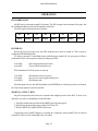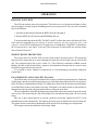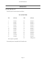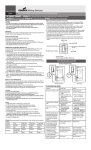
1
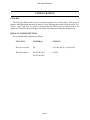
4I20 POWER DRIVER MANUAL
Version 1.0
Copyright 1997 by MESA ELECTRONICS Richmond, CA. Printed in the United States of America.
All rights reserved. This document and the data disclosed herein is not to be reproduced, used,
disclosed in whole or in part to anyone without the written permission of MESA ELECTRONICS.
Mesa Electronics
4175 Lakeside Drive, Suite #100
Richmond, CA 94806-1950
Tel (510) 223-9272 - Fax (510) 223-9585
E-Mail: [email protected] - Website: www.mesanet.com
4I20 USER'S MANUAL
TABLE OF CONTENTS
HANDLING PRECAUTIONS
Static electricity . . . . . . . . . . . . . . . . . . . . . . . . . . . . . . . . . . . . . . . . . . . . . . . . . . . . . . . . . . . . . . . . . . . . . . . . 3
INTRODUCTION
General . . . . . . . . . . . . . . . . . . . . . . . . . . . . . . . . . . . . . . . . . . . . . . . . . . . . . . . . . . . . . . . . . . . . . . . . . . . . . . . . 4
CONFIGURATION
General . . . . . . . . . . . . . . . . . . . . . . . . . . . . . . . . . . . . . . . . . . . . . . . . . . . . . . . . . . . . . . . . . . . . . . . . . . . . . . . .
Default jumper settings . . . . . . . . . . . . . . . . . . . . . . . . . . . . . . . . . . . . . . . . . . . . . . . . . . . . . . . . . . . . . . . .
Base address selection . . . . . . . . . . . . . . . . . . . . . . . . . . . . . . . . . . . . . . . . . . . . . . . . . . . . . . . . . . . . . . . . .
Pullup power jumper . . . . . . . . . . . . . . . . . . . . . . . . . . . . . . . . . . . . . . . . . . . . . . . . . . . . . . . . . . . . . . . . . . .
5
5
7
9
INSTALLATION
General . . . . . . . . . . . . . . . . . . . . . . . . . . . . . . . . . . . . . . . . . . . . . . . . . . . . . . . . . . . . . . . . . . . . . . . . . . . . . . . 11
I/O connector orientation . . . . . . . . . . . . . . . . . . . . . . . . . . . . . . . . . . . . . . . . . . . . . . . . . . . . . . . . . . . . . 11
OPERATION
Bit addressing . . . . . . . . . . . . . . . . . . . . . . . . . . . . . . . . . . . . . . . . . . . . . . . . . . . . . . . . . . . . . . . . . . . . . . . . . 12
Power on. . . . . . . . . . . . . . . . . . . . . . . . . . . . . . . . . . . . . . . . . . . . . . . . . . . . . . . . . . . . . . . . . . . . . . . . . . . . . . 12
Writing output bits . . . . . . . . . . . . . . . . . . . . . . . . . . . . . . . . . . . . . . . . . . . . . . . . . . . . . . . . . . . . . . . . . . . . 12
Reading input bits . . . . . . . . . . . . . . . . . . . . . . . . . . . . . . . . . . . . . . . . . . . . . . . . . . . . . . . . . . . . . . . . . . . . . 13
Short circuit protection . . . . . . . . . . . . . . . . . . . . . . . . . . . . . . . . . . . . . . . . . . . . . . . . . . . . . . . . . . . . . . . 13
Connector pinout . . . . . . . . . . . . . . . . . . . . . . . . . . . . . . . . . . . . . . . . . . . . . . . . . . . . . . . . . . . . . . . . . . . . . 14
4I20TEST . . . . . . . . . . . . . . . . . . . . . . . . . . . . . . . . . . . . . . . . . . . . . . . . . . . . . . . . . . . . . . . . . . . . . . . . . . . . 15
REFERENCE INFORMATION
Specifications . . . . . . . . . . . . . . . . . . . . . . . . . . . . . . . . . . . . . . . . . . . . . . . . . . . . . . . . . . . . . . . . . . . . . . . . . 16
Warranty. . . . . . . . . . . . . . . . . . . . . . . . . . . . . . . . . . . . . . . . . . . . . . . . . . . . . . . . . . . . . . . . . . . . . . . . . . . . . . 17
Schematic diagrams . . . . . . . . . . . . . . . . . . . . . . . . . . . . . . . . . . . . . . . . . . . . . . . . . . . . . . . . . . . . . . . . . . . 19
4I20 USER'S MANUAL
HANDLING PRECAUTIONS
STATIC ELECTRICITY
The CMOS integrated circuits on the 4I20 can be damaged by exposure to electrostatic
discharges. The following precautions should be taken when handling the 4I20 to prevent
possible damage.
A. Leave the 4I20 in its antistatic bag until needed.
B. All work should be performed at an antistatic workstation.
C. Ground equipment into which 4I20 will be installed.
D.
Ground
handling
personnel
with
conductive
bracelet
through
megohm
1
resistor
to
ground.
E. Avoid wearing synthetic fabrics, particularly Nylon.
4I20 USER'S MANUAL
INTRODUCTION
GENERAL
The 4I20 is a stackable PC/104 card with 24 open drain 350 mA outputs for solenoids, valves,
relays, motors, incandescent lamps and other medium power DC loads. The 4I20 outputs are
galvanically isolated from logic ground to avoid ground loops, as the total ground return current be as
much as 8.4 amps. The isolation also allows the 4I20 to drive ground referred loads.
The 4I20 has readback capability on all outputs to verify output switching, and allow unused
outputs to be used as input bits. The output drivers on the 4I20 (TI TIPC6A259) have a built-in 800
mA current limit and are protected against short circuits and capacitive loads with a unique chopping
current limit system.
The outputs have built in 50V clamp diodes to allow driving inductive loads without external
flyback diodes. The 4I20 output connector is a 50 pin header with I/O module compatible pinout
(interleaved grounds), allowing the 4I20 to drive unbuffered OPTO-22 style I/O module racks.
All outputs have optional (plug in) pullup resistors that can be powered from the isolated 5V
power on the 4I20 or external power.
The 4I20 input and output are organized as a 24 bit multiplexer and a 24 bit addressable latch. This
allows simple addressing of single I/O bits. All 4I20 access is through a single 8 bit I/O port.
Page 4
4I20 USER'S MANUAL
CONFIGURATION
GENERAL
The 4I20 port address and I/O power connection options are set with jumpers. Each group of
jumpers will be discussed separately by function. In the following discussions, when the words "up",
"down", "right", and "left" are used it is assumed that the 4I20 I/O card is oriented with its bus
connectors J1 and J2 at the bottom edge of the card (nearest the person doing the configuration).
DEFAULT JUMPER SETTINGS
Factory default 4I20 jumpering is as follows:
FUNCTION
JUMPER(S)
SETTING
4I20 power option
W3
I/O conn. pin 49 = Local power
4I20 Base address
W2,W3,W4,W5,
0300H
W6,W7,W8,W9
Page 5
4I20 USER'S MANUAL
CONFIGURATION
DEFAULT JUMPER SETTINGS
Page 6
4I20 USER'S MANUAL
CONFIGURATION
BASE ADDRESS SELECTION
The base I/O address of the 4I20 card is selected by placing shorting jumpers on jumper blocks
W2 through W9. The 4I20 occupies 4 contiguous locations in I/O space. Jumper blocks W2 through
W9 have three pins and two valid shorting jumper locations, up, and down. The position of jumpers on
W2 through W9 is a binary representation of the 4I20 base address. When a jumper is in the up
position, it matches a high address line.
The following table shows some example base address settings
ADDRESS
W2
W3
W4
W5
W6
W7
W8
W9
(A9)
(A8)
(A7)
(A6)
(A5)
(A4)
(A3)
(A2)
0300H
up
up
down
down
down
down
down
down
0294H
up
down
up
down
down
up
down
up
0368H
up
up
down
up
up
down
up
down
0320H
up
up
down
down
up
down
down
down
Page 7
4I20 USER'S MANUAL
CONFIGURATION
BASE ADDRESS JUMPERS
Page 8
4I20 USER'S MANUAL
CONFIGURATION
PULLUP POWER JUMPER
Pin 49 on the 4I20 I/O connector is connected to the output pullup resistor common. It can either
be connected to the isolated +5V supply on the 4I20 or powered externally.
If external power is used, jumper W1 must pe placed in the right hand position. The externally
supplied voltage must be within the output voltage rating of the 4I20 (48V). With no external load,
the outputs will swing up to (2 (VIN-5)/3) +5) volts.
To use local power, W1 is placed in the left hand position. If local power is used, unloaded outputs
will swing to +5V. The isolated power can be used to supply a very small (5mA) amount of isolated
+5V power if desired. This power is available on pin 49 of the I/O connector.
Make very sure that you do not apply power to pin 49 of the I/O connector if you have the local
power option enabled (W1 left). This can destroy the 4I20 card!
Page 9
4I20 USER'S MANUAL
CONFIGURATION
PULLUP POWER JUMPER
Page 10
4I20 USER'S MANUAL
INSTALLATION
GENERAL
When the 4I20 has been properly configured for its application, it can be inserted into a PC/104
stack. The standoffs should then be tightened to secure the 4I20 in its place. When the 4I20 is secured
in the stack the 50 pin header can be plugged in from the side.
I/O CONNECTOR ORIENTATION
The 50 pin connector on the 4I20 has its pin one end marked with a white square on the circuit
card. This corresponds with the red stripe on typical flat cable assemblies. If more positive
polarization is desired, center polarized IDC header connectors should be used. These connectors
will not fully mate with the pins on the 4I20 if installed backwards. A suggested center polarized 50
pin IDC header is AMP PN 1-746285-0.
Page 11
4I20 USER'S MANUAL
OPERATION
BIT ADDRESSING
All 4I20 access is through a single I/O location. The 4I20 occupies four locations in I/O space, but
the 3 additional addresses are merely duplicates of the first.
The 4I20 register bit functions are as follows:
D7
D6
D5
D4
D3
D2
D1
D0
DATA
POWER
WRITE
BSEL4
BSEL3
BSEL2
BSEL1
BSEL0
POWER ON
Before any I/O access can occur, the 4I20 isolated power must be turned on. This is done by
setting the POWER bit high(D6).
In order to guarantee a controlled startup with all outputs turned off, it is necessary to follow a
predermined 5 byte write sequence when powering up the 4I20:
write 00H
write 40H
(Put output latch in known state)
(Turn on 4I20 isolated power)
Wait a minimum of 1mS for power to come up
write FFH
write 40H
write DFH
(Do dummy write to no-op bit)
(leave power on but toggle all other bits)
(Do dummy read)
All subsequent writes to the 4I20 should have the POWER bit set. If the power bit is ever cleared,
the 5 byte starup sequence must be repeated.
WRITING OUTPUT BITS
Any 4I20 output driver bit can be set or cleared with a single byte write to the 4I20. To write to an
output bit, you write a command byte to the 4I20 that:
1. Specifies the desired output bit with the BSEL bits (bits 0 through 4)
2. Specifies the desired output state with the DATA bit (D7)
3. Has the WRITE (D5) and POWER (D6) bits set
Output bits written with D7 high are set (turned on), output bits written with D7 low are cleared
(turned off). Writes to bits 24 through 31 have no effect.
Page 12
4I20 USER'S MANUAL
OPERATION
READING INPUT BITS
The 4I20 can read the status of its output bits. This can be use to verify output switching, or allow
unused outputs to be used as inputs. Reading inputs is a two step process, First, you write a command
byte to the 4I20 that:
1. Specifies the desired input bit with the BSEL bits (bits 0 through 4).
2. Has the WRITE bit (D5) cleared and POWER bit (D6) set.
You then read the data from the 4I20. The DATA bit (D7) reflects the status of the selected I/O bit
at the time the command byte was written. To poll an input bit, you must repeat the write, read
sequence. A low DATA bit indicates an 'off' output state, or a high input. A high DATA bit indicates
an 'on' output state or a low input. To use an I/O bit as an input, you must make sure that the output
driver for that I/O bit is off.
SHORT CIRCUIT PROTECTION
The output driver ICs that the 4I20 uses have built in short circuit protection. This protection
logic causes the output drivers to start chopping the output drive if the output current exceeds 800
mA. The chopped output duty cycle is about 2%. This effectively constitutes foldback current
limiting. Because of this characteristic, capacitive and incandescent lamp loads may turn on more
slowly than expected or not turn on at all!
It is possible to detect whether an output driver is current limiting by repeatedly reading the
output status.
INCANDESCENT AND CAPACITIVE LOADS
The built-in short circuit protection that the driver chips use limits the maximum size of loads that
exhibit a larger inrush current than operating current. Some loads that exhibit this effect are capacitive
loads, DC motors, and incandescent lamps. To reliably drive these loads, the inrush current should not
exceed the 800 mA short circuit limit of the chip. If this limit is exceeded, the driver chip will not be
damaged, but may stay in the chopping mode and never fully turn on the load.
The rule of thumb for incandescent lamps states that the inrush current is about 10 times the steady
state current. This means that the 4I20 will reliably drive incandecent lamps with a 80 mA current
rating.
One way to drive larger lamps is to provide a preheat resistor that supplies about 25% of the
nominal lamp current continuously. This reduces the inrush current and also increases the lamp life.
The preheat resistor can be driven from another 4I20 output if low operating power is important.
4I20 outputs can also be paralleled to drive larger lamps.
Page 13
4I20 USER'S MANUAL
Page 14
4I20 USER'S MANUAL
OPERATION
CONNECTOR PIN-OUT
The 4I20 50 pin I/O connector pinout is as follows:
P1 CONNECTOR
PIN
SIGNAL
PIN
SIGNAL
1
I/O bit 0
25
I/O bit 12
3
I/O bit 1
27
I/O bit 13
5
I/O bit 2
29
I/O bit 14
7
I/O bit 3
31
I/O bit 15
9
I/O bit 4
33
I/O bit 16
11
I/O bit 5
35
I/O bit 17
13
I/O bit 6
37
I/O bit 18
15
I/O bit 7
39
I/O bit 19
17
I/O bit 8
41
I/O bit 20
19
I/O bit 9
43
I/O bit 21
21
I/O bit 10
45
I/O bit 22
23
I/O bit 11
47
I/O bit 23
49
Pullup power
All even pins are grounded
Note that this pinout is compatible with I/O module racks.
Page 15
4I20 USER'S MANUAL
OPERATION
4I20TEST
A simple test program is supplied with the 4I20 for functional testing and verification. This
program is called 4I20TEST.EXE. 4I20TEST performs a rotating bit test of all 24 I/O bits. You must
not haveI/O cable attached to the 4I20 when running this test.
4I20TEST is invoked with the 4I20 base address (in hex) on the command line.
4I20TEST 300
Would test the 4I20 at the default (0300H) base address. 4I20TEST prints a '*' every good pass
and can be aborted by pressing any key.
Page 16
4I20 USER'S MANUAL
REFERENCE INFORMATION
SPECIFICATIONS
MIN
MAX
UNIT
Voltage
4.5
5.5
V
Supply current
---
50
mA
Input capacitance
---
15
pF
Input leakage current
---
5
uA
Output drive capability
150
---
pF
Output sink current
12
---
mA
Input logic low
-.3
.8
V
Input logic high
2.0
48
V
Output on state voltage
----
.5
V
Output off state voltage
---
48
V
-40
+85
o
o
POWER SUPPLY
(no ext. load)
BUS LOADING:
I/O BIT SPECIFICATIONS:
350 mA sink
ENVIRONMENTAL:
Operating temperature range
-I version
-C version
0
+70
Relative humidity
0
90
C
C
Percent
Non-condensing
Page 17
4I20 USER'S MANUAL
REFERENCE INFORMATION
WARRANTY
Mesa Electronics warrants the products it manufactures to be free effects in material and
workmanship under normal use and service for the period of 2 years from date of purchase. This
warranty shall not apply to products which have been subject to misuse, neglect, accident, or
abnormal conditions of operation.
In the event of failure of a product covered by this warranty, Mesa Electronics, will repair any product
returned to Mesa Electronics within 2 years of original purchase, provided the warrantor's
examination discloses to its satisfaction that the product was defective. The warrantor may at its
option, replace the product in lieu of repair.
With regard to any product returned within 2 years of purchase, said repairs or replacement will be
made without charge. If the failure has been caused by misuse, neglect, accident, or abnormal
conditions of operation, repairs will be billed at a nominal cost.
THE FOREGOING WARRANTY IS IN LIEU OF ALL OTHER WARRANTIES,
EXPRESS OR IMPLIED. INCLUDING BUT NOT LIMITED TO ANY IMPLIED
WARRANTY OF MERCHANTABILITY, FITNESS, OR ADEQUACY FOR ANY
PARTICULAR PURPOSE OR USE. MESA ELECTRONICS SHALL NOT BE LIABLE FOR
ANY SPECIAL, INCIDENTAL, OR CONSEQUENTIAL DAMAGES, WHETHER IN
CONTRACT, TORT, OR OTHERWISE.
If any failure occurs, the following steps should be taken:
1. Notify Mesa Electronics, giving full details of the difficulty. On receipt of this information,
service data, or shipping instructions will be forwarded to you.
2. On receipt of the shipping instructions, forward the product, in its original protective
packaging, transportation prepaid to Mesa Electronics. Repairs will be made at Mesa Electronics and
the product returned transportation prepaid.
Page 18
4I20 USER'S MANUAL
Page 19