1
VadaTech AMC520
User’s Manual
July 18, 2014
Version 2.2.2
THE POWER OF VISION
VadaTech AMC520 User’s Manual
Copyright
© 2014 VadaTech Incorporated
All rights reserved
VadaTech and the globe image are trademarks of VadaTech Incorporated.
All other product or service names mentioned in this document are the property of their
respective owners.
Notice
While reasonable efforts have been made to assure the accuracy of this document,
VadaTech, Inc. assumes no liability resulting from any omissions in this document or from
the use of the information obtained herein. VadaTech reserves the right to revise this
document and to make changes periodically and the content hereof without obligation of
VadaTech to notify any person of such revision or changes.
Electronic versions of this material may be read online, downloaded for personal use, or
referenced in another document as a URL to the VadaTech Incorporated Web site. The text
itself may not be published commercially in print or electronic form, edited, translated, or
otherwise altered without the permission of VadaTech, Inc.
It is possible that this publication may contain reference to or information about VadaTech
products (machines and programs), programming, or services that are not available in your
country. Such references or information must not be construed to mean that VadaTech
intends to announce such products, programming, or services in your country.
Trademarks
The VadaTech, Inc name and logo are registered trademarks of VadaTech Incorporated in
the U.S.A. All other product or service names mentioned in this document are the property
of their respective owners.
© 2014, VadaTech Incorporated. Printed in the U.S.A., All Rights Reserved.
VADATECH FORM No. 3WI731-01 Rev. B
VT-MAN-CUS-100402-2.2.1
Page 2 of 101
VadaTech AMC520 User’s Manual
Revision History
Doc
Rev
0.0.1
1.0.0
2.0.0
2.0.1
2.1.0
2.2.0
2.2.1
2.2.2
Description of Change
Initial version
Documentation completed
Updated entire document to match Rev B board.
Updated document to match Rev C board and software.
Clarified the size and configurations of the QDRII+ SRAM.
Added section describing how to modify the hardware to
convert channels between OpAmp and Magnetic after
purchase.
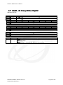
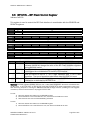
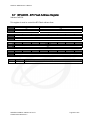
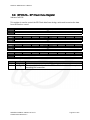
Added CREN:USERIOTEST and CREN:RTMTEST registers fields
and associated description to enable the front panel User I/O
and RTM Data/Clock loopback diagnostic tests.
Added board photo.
Provided an improved block diagram.
Added Front Panel User I/O connector description.
Added capture and capture_all script description to simplify
ADC data capture process.
Expanded the DACCTRL:FIXED_GENx fields and added the
DACFD register to allow arbitrary fixed data value to be
presented to the DAC channels.
Changes to add DAC loop-through from ADC channels feature:
Added description of the DAC loop-through feature.
Added DAC MMCM status bits to BRDSTATUS register.
Expanded the DACCTRL:FIXED_GENx fields and dropped the
FIXED_ portion of the name to add values for each ADC
channel.
VADATECH FORM No. 3WI731-01 Rev. B
VT-MAN-CUS-100402-2.2.1
Revision Date
2/7/2012
4/4/2012
9/15/2012
10/14/2013
3/18/2014
7/16/2014
7/17/2014
7/18/2014
Page 3 of 101
VadaTech AMC520 User’s Manual
Table of Contents
1 Document Overview ............................................................................................................... 9 1.1 Applicable Products......................................................................................................... 9 1.2 Document References .................................................................................................... 9 1.3 Acronyms Used in this Document ................................................................................ 10 2 Hardware Overview .............................................................................................................. 12 2.1 Block Diagram ............................................................................................................... 14 2.2 Board Layout.................................................................................................................. 15 2.3 On-board Switches ........................................................................................................ 17 2.4 On-board Headers/Jumpers ......................................................................................... 17 2.5 FPGA Debug Test Points ............................................................................................... 18 2.6 Front Panel Interfaces................................................................................................... 18 2.6.1 Front Panel IPMI LEDs and Hot-Swap Handle...................................................... 18 2.6.2 Front Panel IPMI RS-232 Port ............................................................................... 19 2.6.3 Front Panel FPGA RS-232 Port.............................................................................. 19 2.6.4 Front Panel SFP+ Ports.......................................................................................... 20 2.6.5 Front Panel FPGA STATUS LEDs............................................................................ 20 2.6.6 Front Panel User LEDs ........................................................................................... 21 2.6.7 Front Panel FPGA DONE LED................................................................................. 21 2.6.8 Front Panel PCIe LEDs ........................................................................................... 21 2.6.9 Front Panel FPGA JTAG Port .................................................................................. 21 2.6.10 Front Panel CLK IN Port ..................................................................................... 22 2.6.11 Front Panel TRIG IN Port .................................................................................... 22 2.6.12 Front Panel TRIG OUT Port ................................................................................. 23 2.6.13 Front Panel User I/O .......................................................................................... 23 2.7 On-board ADC/DAC Clock Routing ............................................................................... 24 2.8 On-board Trigger Routing .............................................................................................. 26 2.9 On-board QDRII+ / IODELAY Calibration / Misc Clocking ........................................... 27 2.10 Backplane/RTM Connections ................................................................................... 27 2.1 FPGA Banking/Pinning/Floorplan ................................................................................ 28 2.2 FPGA SERDES Backplane Interfaces ........................................................................... 28 2.3 FPGA SERDES Front Panel Interfaces .......................................................................... 28 2.4 FPGA SERDES Reference Clocks.................................................................................. 29 2.5 Backplane/On-board PCIe Clock Routing (CLK3/FCLKA) ........................................... 30 2.6 On-board 125MHz Clock Routing ................................................................................. 31 2.7 ADC Channel Coupling (Magnetic vs. OpAmp) ............................................................ 32 3 IPMI MMC Serial Menu Interface ........................................................................................ 34 3.1 E-Keying Configuration .................................................................................................. 34 4 IPMI Sensors ........................................................................................................................ 35 5 FPGA Reference Design....................................................................................................... 36 5.1 FPGA Reference Design External Interfaces ............................................................... 36 5.2 FPGA Reference Design Internals ................................................................................ 37 5.2.1 PCIe Bridge (pcie_local_bridge.vhd) ..................................................................... 39 VADATECH FORM No. 3WI731-01 Rev. B
VT-MAN-CUS-100402-2.2.1
Page 4 of 101
VadaTech AMC520 User’s Manual
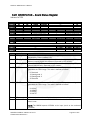
5.2.2 Interrupt Controller (vt_interrupt_controller_x32.vhd) ........................................ 40 5.2.3 Clock Router (clock_router.vhd) ............................................................................ 40 5.2.4 LED Controller (leds.vhd) ....................................................................................... 40 5.2.5 ADC Chip Controller (adc_chip.vhd) ...................................................................... 40 5.2.6 ADC Channel (adc_chan.vhd) ................................................................................ 40 5.2.7 ADC SPI Master (adc_spi.vhd)............................................................................... 40 5.2.8 ADC Synchronizer (adc_sync.vhd)......................................................................... 41 5.2.9 ADC Selector (adc_selector.vhd)........................................................................... 41 5.2.10 DAC Chip Controller (dac_chip.vhd) .................................................................. 41 5.2.11 DAC Channel (dac_channel.vhd) ....................................................................... 41 5.2.12 BPI Flash Core (bpi_flash.vhd) .......................................................................... 41 5.2.13 SYSMON Core (sysmon_core.vhd) .................................................................... 42 5.2.14 Utility Core (vt_utility_x32.vhd) .......................................................................... 42 5.2.15 Miscellaneous Helper Cores .............................................................................. 42 5.2.16 Xilinx IP Cores ..................................................................................................... 42 6 Customer FPGA Development ............................................................................................. 44 6.1 Modular FPGA Project Design....................................................................................... 45 6.2 FPGA Development/Debug Cycle ................................................................................. 46 7 Host-side Software Support ................................................................................................ 47 7.1 AMC520 Device Driver .................................................................................................. 47 7.2 AMC520 Tool Application ............................................................................................. 48 8 Appendix A: FPGA PCIe Register Specification................................................................... 51 8.1 FPGA Reference Design PCIe Config Space ................................................................ 51 8.2 GIMSR – Global Interrupt Mask Set Register .............................................................. 55 8.3 GIMCR – Global Interrupt Mask Clear Register ........................................................... 56 8.4 GISR – Global Interrupt Status Register ...................................................................... 57 8.5 BCSR – Bit Change Status Register ............................................................................. 58 8.6 BPICTRL - BPI Flash Control Register ........................................................................... 59 8.7 BPIADDR - BPI Flash Address Register ........................................................................ 60 8.8 BPIDATA - BPI Flash Data Register ............................................................................... 61 8.9 CREN – Clock Routing Enable Register ....................................................................... 62 8.10 CRTCLKA/B/C/D/TRIGSTART/TRIGEND/TRIGOUT – Clock Routing Registers ..... 64 8.11 DACCTRL – DAC Control Register ............................................................................. 66 8.12 DACDELAY – DAC Delay Register.............................................................................. 68 8.13 DACFD – DAC Fixed Data Register ........................................................................... 69 8.14 ADCCTRL0/1/2/3/4 – ADC Chip 0/1/2/3/4 Control Registers ............................ 70 8.15 ADCDELAY0/1/2/3/4 – ADC Chip 0/1/2/3/4 Delay Registers ............................ 71 8.16 ADCBIST[0/1]0/1/2/3/4 – ADC Chip 0/1/2/3/4 BIST 0/1 Registers ................. 72 8.17 SPICTRL0/1/2/3/4 – ADC Chip 0/1/2/3/4 SPI Control Register......................... 73 8.18 SYNCCTRL – ADC Synchronizer Control Register .................................................... 74 8.19 SYNCDELAY – ADC Synchronizer Delay Register..................................................... 75 8.20 ADCSEL – ADC Selector Register.............................................................................. 76 8.21 ADCDATA – ADC Data Register ................................................................................. 77 8.22 TEMP – FPGA Temperature Register........................................................................ 78 8.23 VCCINT – FPGA Internal Voltage Register ................................................................ 79 8.24 VCCAUX – FPGA Auxiliary Voltage Register .............................................................. 80 8.25 BRDSTATUS – Board Status Register....................................................................... 81 VADATECH FORM No. 3WI731-01 Rev. B
VT-MAN-CUS-100402-2.2.1
Page 5 of 101
VadaTech AMC520 User’s Manual
8.26 A0/1STATUS – AMC Port 0/1 Status Registers ...................................................... 83 8.27 A2/3STATUS – AMC Ports 4-7/8-11 Status Registers............................................ 84 8.28 SCRATCH – Scratch Register .................................................................................... 85 8.29 VER – FPGA Version Register.................................................................................... 86 8.30 SIG –Signature Register ............................................................................................ 87 9 Appendix B: Linux Device Driver IOCTL Spec ..................................................................... 88 9.1 AMC520_IOC_GET_INFO .............................................................................................. 88 9.2 AMC520_IOC_GET_BCISTATUS .................................................................................... 89 9.3 AMC520_IOC_GET/SET_CLOCK_ROUTING ................................................................. 90 9.4 AMC520_IOC_GET_PORTSTATUS ................................................................................ 91 9.5 AMC520_IOC_GET/SET_REG ....................................................................................... 92 9.6 AMC520_IOC_GET/SET_EXREG ................................................................................... 92 9.7 AMC520_IOC_GET_SYSMON........................................................................................ 92 9.8 AMC520_IOC_GET/SET_ADCCTRL............................................................................... 93 9.9 AMC520_IOC_GET/SET_ADCSEL ................................................................................. 94 9.10 AMC520_IOC_GET_ADCDATA ................................................................................... 94 9.11 AMC520_IOC_GET/SET_ADCREG ............................................................................ 95 9.12 AMC520_IOC_GET/SET_SYNCCTRL ......................................................................... 95 9.13 AMC520_IOC_GET/SET_DACCTRL ........................................................................... 96 9.14 AMC520_IOC_GET/SET_DACDELAY ......................................................................... 97 9.15 AMC520_IOC_GET/SET_SYNCDELAY ...................................................................... 97 9.16 AMC520_IOC_GET/SET_ADCDELAY ......................................................................... 98 9.17 AMC520_IOC_FLASH_OP .......................................................................................... 99 10 Appendix C: AMC520 Card-edge Pin-out ......................................................................... 100 11 Appendix D: AMC520 RTM Pin-out .................................................................................. 101 VADATECH FORM No. 3WI731-01 Rev. B
VT-MAN-CUS-100402-2.2.1
Page 6 of 101
VadaTech AMC520 User’s Manual
Figures
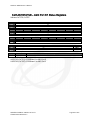
Figure 1: AMC520 board photo .................................................................................................. 12 Figure 2: AMC520 simplified block diagram .............................................................................. 14 Figure 3: AMC520 top-side layout (front towards right) ............................................................ 15 Figure 4: AMC520 bottom-side layout (front towards left)........................................................ 16 Figure 5: AMC520 front panel..................................................................................................... 18 Figure 6: Front panel CLK IN circuit ............................................................................................ 22 Figure 7: Front panel TRIG IN circuit........................................................................................... 22 Figure 8: Front panel TRIG OUT circuit ....................................................................................... 23 Figure 9: On-board ADC/DAC Clock Routing .............................................................................. 25 Figure 10: On-board trigger routing ............................................................................................ 26 Figure 11: QDRII+, IODELAY calibration, and misc clock routing ............................................. 27 Figure 12: Virtex 6 GTX clock forwarding for AMC520 .............................................................. 29 Figure 13: PCIe clock routing ...................................................................................................... 30 Figure 14: 125MHz clock routing ............................................................................................... 31 Figure 15: ADC Coupling Zero-Ohm Resistors Location ............................................................ 32 Figure 16: ADC Channel Coupling: Channels 0/1 Magnetic Example ..................................... 33 Figure 17: ADC Channel Coupling: Channels 0/1 OpAmp Example ......................................... 33 Figure 18: AMC520 FPGA Top-Level Reference Design Diagram ............................................ 37 Figure 19: AMC520 FPGA ADC Reference Design Diagram ..................................................... 38 Figure 20: AMC520 FPGA DAC Reference Design Diagram ..................................................... 39 VADATECH FORM No. 3WI731-01 Rev. B
VT-MAN-CUS-100402-2.2.1
Page 7 of 101
VadaTech AMC520 User’s Manual
Tables
Table 1: Acronyms....................................................................................................................... 11 Table 2: SW5 settings .................................................................................................................. 17 Table 3: P7 TRIG IN termination header .................................................................................... 17 Table 4: P8 CLK IN termination header...................................................................................... 17 Table 5: FPGA Debug Test Points ............................................................................................... 18 Table 6: AMC LED behavior ......................................................................................................... 18 Table 7: IPMI RS-232 port pin-out .............................................................................................. 19 Table 8: FPGA RS-232 port pin-out ............................................................................................. 20 Table 9: STATUS LED usage in Reference Design ..................................................................... 20 Table 10: FPGA User LEDs .......................................................................................................... 21 Table 11: FPGA JTAG Pin-out ....................................................................................................... 21 Table 12: USER IO 0/7 Connector .............................................................................................. 23 Table 13: USER IO 8/15 Connector............................................................................................ 23 Table 14: Selecting the ADC clock source ................................................................................. 24 Table 15: FPGA reference design backplane SERDES interfaces ............................................ 28 Table 16: FPGA reference design backplane SERDES interfaces ............................................ 28 Table 17: ADC Channel Coupling Resistors ............................................................................... 33 Table 18: MMC Sensors .............................................................................................................. 35 Table 19: Modular FPGA Project Variations ............................................................................... 45 Table 20: FPGA reference design PCIe device/vendor IDs ....................................................... 51 Table 21: FPGA reference design PCIe BAR configuration ....................................................... 51 Table 22: FPGA reference design register map ......................................................................... 54 Table 23: AMC520 card-edge pin-out ..................................................................................... 100 Table 24: AMC520 J30 Pin-out ................................................................................................ 101 Table 25: AMC520 J31 Pin-out ................................................................................................ 101 VADATECH FORM No. 3WI731-01 Rev. B
VT-MAN-CUS-100402-2.2.1
Page 8 of 101
VadaTech AMC520 User’s Manual
1 Document Overview
This document describes the AMC520 board including the FPGA reference design, host-side
device driver/tool, and configuration of the MMC microcontroller. It also describes how to go
about using/customizing the FPGA reference design for customer specific needs.
Further FPGA/software development is generally expected to be performed at the
customer’s site to add any additional application-specific functionality to the AMC520 board.
The reference design FPGA/software implementation is provided as an example and proofof-concept but is not considered a formal baseline for the customer’s application and it may
change at any time.
This document describes the Rev C and later version of the board. Prior board versions are
not supported.
1.1 Applicable Products
VadaTech AMC520 (Virtex-6)
Related product:
o VadaTech AMC514 (Virtex-6 - AMC520 derives from this design)
1.2 Document References
AMC520 FPGA Pin-out/Design Diagrams (found in AMC520 VHDL Sources release)
VadaTech AMC520 Datasheet (http://www.vadatech.com)
PICMG® AMC.0 R2.0 AdvancedMC Mezzanine Module (http://www.picmg.org)
PICMG® AMC.1 R2.0 AdvancedMC PCI Express and AS (http://www.picmg.org)
PICMG® AMC.2 R1.0 AdvancedMC Ethernet (http://www.picmg.org)
PICMG® uTCA.4 R1.0 Enhancements for Rear I/O and Precision Timing
(http://www.picmg.org)
Xilinx Virtex-6 Datasheets and User’s Guides
(http://www.xilinx.com/support/documentation/virtex-6.htm)
Xilinx Virtex-6 Integrated Block for PCI Express (PCIe) Documentation
(http://www.xilinx.com/products/ipcenter/V6_PCI_Express_Block.htm)
Xilinx Virtex-6 Embedded Tri-Mode Ethernet MAC Wrapper Documentation
(http://www.xilinx.com/products/ipcenter/V6_Embedded_TEMAC_Wrapper.htm)
Xilinx XAUI Documentation (http://www.xilinx.com/products/ipcenter/XAUI.htm)
Xilinx Memory Interface Generator Documentation
(http://www.xilinx.com/products/ipcenter/MIG.htm)
VADATECH FORM No. 3WI731-01 Rev. B
VT-MAN-CUS-100402-2.2.1
Page 9 of 101
VadaTech AMC520 User’s Manual
1.3 Acronyms Used in this Document
Acronym
A/D
ADC
AMC
BAR
BIST
BPI
CGND
CLK
CPU
D/A
DAC
DDR3
DIP
DMUX
DR
FPGA
FRU
GbE
GND
GTX
ioctl
IP
IPMI
JSM
JTAG
LED
LVCMOS
LVDS
MAC
MB
MIG
M-LVDS
mmap
MMC
MMIO
MUX
n.c.
PCIe
PHY
PICMG
PIO
SDRAM
SERDES
SGMII
Description
Analog to Digital Converter
Analog to Digital Converter
Advanced Mezzanine Card
Base Address Register
Built-In Self Test
Byte Peripheral Interface
Chassis Ground
Clock
Central Processing Unit
Digital to Analog Converter
Digital to Analog Converter
Dual Data Rate 3 SDRAM
Dual In-line Package
De-multiplexer
Data Ready
Field Programmable Gate Array
Field Replaceable Unit
Gigabit Ethernet
Signal Ground
Virtex-6 Gigabit Transceiver
Input/Output/Control
Intellectual Property / Internet Protocol
Intelligent Platform Management Interface
JTAG Switch Module
Joint Test Action Group
Light Emitting Diode
Low-Voltage Complementary Metal Oxide Semiconductor
Low Voltage Differential Signaling
Media Access Controller
Megabyte (2^20 bytes)
Memory Interface Generator
Multi-point Low Voltage Differential Signaling
Memory Map
Module Management Controller
Memory Mapped Input/Output
Multiplexer
No connection
Peripheral Component Interconnect Express
Physical Layer Device
PCI Industrial Computer Manufacturer’s Group
Programmed Input/Output
Synchronous Dynamic Random Access Memory
Serializer/Deserializer
Serial Gigabit Medium Independent Interface
VADATECH FORM No. 3WI731-01 Rev. B
VT-MAN-CUS-100402-2.2.1
Page 10 of 101
VadaTech AMC520 User’s Manual
TCLK
TRN
Telephony Clock
Transaction (layer of PCIe implementation)
Table 1: Acronyms
VADATECH FORM No. 3WI731-01 Rev. B
VT-MAN-CUS-100402-2.2.1
Page 11 of 101
VadaTech AMC520 User’s Manual
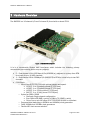
2 Hardware Overview
The AMC520 is a 10-channel A/D and 2-channel D/A card with on-board FPGA.
Figure 1: AMC520 board photo
It is in a double-wide Physics AMC form-factor which includes the following primary
components (your ordering option may vary slightly):
5 – Dual-channel 16-bit 125 Msps A/Ds (AD9268) w/ magnetic or op-amp from RTM
for a total of up to 10 ADC channels
1 – Dual-channel 16-bit 250Msps D/A (MAX5878) to RTM for a total of up to two DAC
channels
FPGA Block:
o Xilinx Virtex-6 FF1759 FPGA with optional density and speed:
LX240T -1 or -2 (partially pinned FF1759 part)
LX365T -1 or -2 (partially pinned FF1759 part)
LX550T -1 or -2 (fully pinned FF1759 part)
SX475T -1 or -2 (fully pinned FF1759 part)
o Option for QDRII+ SRAM
Channels: Single channel configuration
Size: 2Mbit x36 (8MB + parity) or 2Mbit x72 (16MB + parity)
Chips: One or two x36 chips of CY7C25652KV18-400 or equivalent
o Programmable (defaulting to 300MHz and 400MHz) clock generators
o Fixed 100MHz and 125MHz clock generators
o Flexible ADC clock source selection
VADATECH FORM No. 3WI731-01 Rev. B
VT-MAN-CUS-100402-2.2.1
Page 12 of 101
VadaTech AMC520 User’s Manual
o Backplane M-LVDS Clock/Trigger Transceivers (SN65MLVD080)
o Backplane PCIe 2x4 or x8 connectivity w/ active repeaters (AMC Ports 4-11)
o Backplane Dual 1000Base-X connectivity (AMC Ports 0 & 1)
o Backplane Arbitrary SERDES connectivity (AMC Ports 2 & 3 and 12-15)
o Front panel Dual SFP+ cages
o 4 – User LEDs
o 16 – Status LEDs
o FPGA Configuration DONE LED
o Front panel CLK IN / TRIG IN / TRIG OUT
o 16 – Front panel Arbitrary USER I/O
o Front panel FPGA JTAG (switchable to backplane JSM)
o RS-232 console port
o 32MB BPI Configuration Flash (JS28F256P30T or equivalent)
AMC MMC controller w/ IPMI LEDs, hot swap handle, RS-232, etc
VADATECH FORM No. 3WI731-01 Rev. B
VT-MAN-CUS-100402-2.2.1
Page 13 of 101
VadaTech AMC520 User’s Manual
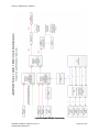
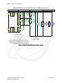
2.1 Block Diagram
AMC Card Edge
AMC Front Panel
RTM Connector
A simplified block diagram is shown below:
Figure 2: AMC520 simplified block diagram
VADATECH FORM No. 3WI731-01 Rev. B
VT-MAN-CUS-100402-2.2.1
Page 14 of 101
VadaTech AMC520 User’s Manual
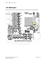
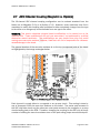
2.2 Board Layout
The top-side layout of the card is shown below which includes user accessible jumpers:
P8
P7
Figure 3: AMC520 top-side layout (front towards right)
VADATECH FORM No. 3WI731-01 Rev. B
VT-MAN-CUS-100402-2.2.1
Page 15 of 101
VadaTech AMC520 User’s Manual
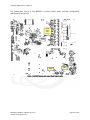
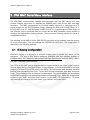
The bottom-side layout of the AMC520 is shown below which includes configuration
switches and test points:
FPGA
DEBUG
TEST
POINTS
SW6
SW5
Figure 4: AMC520 bottom-side layout (front towards left)
VADATECH FORM No. 3WI731-01 Rev. B
VT-MAN-CUS-100402-2.2.1
Page 16 of 101
VadaTech AMC520 User’s Manual
2.3 On-board Switches
The card includes a set of DIP switches at SW5 which control miscellaneous board functions
as shown below:
SW51
2
3
4
Off
Reserved [factory default]
Reserved [factory default]
Direct FPGA JTAG to front panel [factory default]
Flash NOT write protected [factory default]
On
Reserved (do not set)
Reserved (do not set)
Direct FPGA JTAG to AMC connector (JSM)
Flash write protected
Table 2: SW5 settings
The card includes a set of DIP switches at SW6 which control the MMC microcontroller and
are reserved for VadaTech use. These default to OFF-OFF-OFF-OFF, please do not change
the setting without instruction from VadaTech.
2.4 On-board Headers/Jumpers
The jumper P7 enables 50ohm parallel termination for the TRIG IN front panel port.
Pin
Shunted
1-2 50ohm termination
Open
100Kohm weak pull-down
Table 3: P7 TRIG IN termination header
The jumper P8 enables 50ohm parallel termination for the CLK IN front panel port.
Pin
Shunted
1-2 50ohm termination
Open
100Kohm weak pull-down
Table 4: P8 CLK IN termination header
VADATECH FORM No. 3WI731-01 Rev. B
VT-MAN-CUS-100402-2.2.1
Page 17 of 101
VadaTech AMC520 User’s Manual
2.5 FPGA Debug Test Points
Test points are conveniently located within a silkscreen box on the back of the board to
provide additional debug capability. They are listed in the order in which they appear within
the box on the board.
Test
Point
TP262
TP255
TP253
TP254
TP251
TP250
TP247
TP242
VHDL Name
FPGA Pin
DEBUG(0)
DEBUG(1)
DEBUG(2)
DEBUG(3)
DEBUG(4)
DEBUG(5)
DEBUG(6)
DEBUG(7)
F12
E12
B16
A16
H15
G14
D16
C16
Table 5: FPGA Debug Test Points
2.6 Front Panel Interfaces
The front panel of the AMC520 is shown below:
Figure 5: AMC520 front panel
2.6.1 Front Panel IPMI LEDs and Hot-Swap Handle
The front panel includes the standard AMC IPMI LEDs showing hot-swap status and general
card health. The LEDs behave as follows:
LED
Blue
Red
Green
Amber
Off
Card active
No Fault
No payload power
Normal
On
OK to remove
Payload Power Fault
Payload power OK
n/a
Blink
Hot-swap/power transitioning
n/a
E-Keying failure
MMC flash writing
Table 6: AMC LED behavior
VADATECH FORM No. 3WI731-01 Rev. B
VT-MAN-CUS-100402-2.2.1
Page 18 of 101
VadaTech AMC520 User’s Manual
NOTE: The card should only be removed from a running carrier when the IPMI Blue LED is
solid ON.
To insert the card, pull out the hot-swap handle until it stops. Insert the card into the
carrier’s guide rails and push on the front panel firmly until it is fully seated into the
connector. If the card does not go fully in, do not force it and instead remove it and check
for proper orientation or obstructions. Once fully inserted the Blue LED should go to solid
ON while the Green LED should start blinking. Then push in the handle to latch the card into
the carrier, the Blue LED should blink for a time and then go solid OFF while the Green LED
goes solid ON.
To remove the card, pull out the hot-swap handle until it stops to unlatch the card from the
carrier (but do not pull hard enough to remove the card itself yet). The Blue LED should
blink for a time and then go solid ON. Once it does, pull the hot-swap handle straight out
firmly to remove the card from the carrier.
2.6.2 Front Panel IPMI RS-232 Port
An IPMI RS-232 port is provided on the front panel for connecting to the MMC CPU. This
port is used for configuration of AMC E-Keying using a menu interface (see subsequent
section). A VadaTech cable (P/N CBL-DB9MUSB1) is available for converting this port into a
DB9 serial port. The port setup is 115200-8-N-1-NOFLOW. The pin-out is as follows:
Pin
1
2
3
4
5
SHIELD
Signal
n.c.
RXD
TXD
n.c.
GND
CGND
Table 7: IPMI RS-232 port pin-out
WARNING: This port uses the MicroUSB form factor but DOES NOT carry USB signaling.
Therefore please be careful not to attach any USB device to the AMC520 board as damage
could result.
2.6.3 Front Panel FPGA RS-232 Port
A CPU/FPGA RS-232 port is provided on the front panel which is routed to the FPGA to
enable it to be used by a soft CPU core in the FPGA if desired. A VadaTech cable (P/N CBLDB9MUSB1) is available for converting this port into a DB9 serial port. The port setup is
115200-8-N-1-NOFLOW.
VADATECH FORM No. 3WI731-01 Rev. B
VT-MAN-CUS-100402-2.2.1
Page 19 of 101
VadaTech AMC520 User’s Manual
The pin-out is as follows:
Pin
1
2
3
4
5
SHIELD
Signal
n.c.
RXD
TXD
n.c.
GND
CGND
Table 8: FPGA RS-232 port pin-out
WARNING: This port uses the MicroUSB form factor but DOES NOT carry USB signaling.
Therefore please be careful not to attach any USB device to the AMC520 board as damage
could result.
2.6.4 Front Panel SFP+ Ports
The front panel hosts two SFP+ ports which route directly to FPGA SERDES ports. In addition
to the SERDES the SFP+ ports provide RXLOS (RX Loss of Signal) and TX_FAULT (TX Fault)
indications to the FPGA as well as TX_DISABLE (TX Disable) control from the FPGA.
2.6.5 Front Panel FPGA STATUS LEDs
There is a grouping of 16 STATUS LEDs on the front panel with the first 12 of them being
green and the last four being yellow. These LEDs are connected to the FPGA for displaying
arbitrary status information in the customer’s application. The usage of these LEDs by the
FPGA reference design is shown below (but does not constrain the customer’s application to
using them for these purposes):
LED
0
1
2
3
Reference
Design Usage
ADC 0/1 Running
ADC 2/3 Running
ADC 4/5 Running
ADC 6/7 Running
LED
4
5
6
7
Reference Design LED
Reference Design
Usage
Usage
ADC 8/9 Running
8
MMCMs Locked
DAC 0/1 Running
9
QDRII+ BIST OK
SFP+ 0 SYNCed
10
SFP+ 0 Signal Detected
SFP+ 1 SYNCed
11
SFP+ 1 Signal Detected
Table 9: STATUS LED usage in Reference Design
LED
12
13
14
15
Reference Design
Usage
FPGA main reset
QDRII+ Calibrating
PCIe 4-7 PCIe TRN reset
PCIe 4-7 not x4
NOTE: The FPGA reference design implements a power-on lamp test mode for these LEDs.
After the FPGA loads it will turn all of these LEDs on for one second then off for one second,
after which it displays the status information as shown above. Also note that it is normal for
the QDRII+ to not finish calibration if the board is ordered without QDRII+ chips.
VADATECH FORM No. 3WI731-01 Rev. B
VT-MAN-CUS-100402-2.2.1
Page 20 of 101
VadaTech AMC520 User’s Manual
2.6.6 Front Panel User LEDs
The front panel includes four green User LEDs which are controlled via the FPGA. The FPGA
reference design uses these LEDs in the following manner (but does not constrain the
customer’s application to using them for these purposes):
LED
U0
U1
U2
U3
Reference Design Usage
Backplane FPGA 1000Base-X Port 0 SYNCed
Backplane FPGA 1000Base-X Port 1 SYNCed
Backplane FPGA PCIe 4-7 Linked
Backplane FPGA PCIe 8-11 Linked
Table 10: FPGA User LEDs
NOTE: The FPGA reference design implements a power-on lamp test mode for these LEDs.
After the FPGA loads it will turn all of these LEDs on for one second then off for one second,
after which it displays the status information as shown above.
2.6.7 Front Panel FPGA DONE LED
A green FPGA DONE LED is lit to indicate that the FPGA configuration loaded successfully.
2.6.8 Front Panel PCIe LEDs
The front panel includes eight green LEDs showing PCIe RX signal detection (Root Complex
is sending PCIe signals) and eight green LEDs showing PCIe TX signal detection (FPGA is
sending PCIe signals). These LEDs are driven by the on-board PCIe repeaters.
2.6.9 Front Panel FPGA JTAG Port
The front panel includes a JTAG port which is routed to the Xilinx Virtex-6 FPGA on the board
when SW5[3] is set to OFF. This port can be connected to a Xilinx Platform USB II cable (or
equivalent) and has the following pin-out:
Pin
1
3
5
7
9
11
13
Signal
GND
GND
GND
GND
GND
GND
GND
Pin
2
4
6
8
10
12
14
Signal
+2.5V
TMS
TCK
TDO
TDI
n.c.
n.c.
Table 11: FPGA JTAG Pin-out
VADATECH FORM No. 3WI731-01 Rev. B
VT-MAN-CUS-100402-2.2.1
Page 21 of 101
VadaTech AMC520 User’s Manual
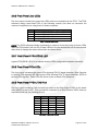
2.6.10 Front Panel CLK IN Port
There is a CLK IN port provided on the front panel via an MMCX jack. This clock input is one
possible source for the ADC clock distribution.
The clock input uses the following circuit:
Figure 6: Front panel CLK IN circuit
The input is LVTTL w/ 5V tolerance.
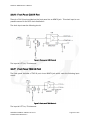
2.6.11 Front Panel TRIG IN Port
The front panel includes a TRIG IN port via an MMCX jack which uses the following input
circuit:
Figure 7: Front panel TRIG IN circuit
The input is LVTTL w/ 5V tolerance.
VADATECH FORM No. 3WI731-01 Rev. B
VT-MAN-CUS-100402-2.2.1
Page 22 of 101
VadaTech AMC520 User’s Manual
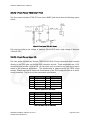
2.6.12 Front Panel TRIG OUT Port
The front panel includes a TRIG OUT port via an MMCX jack which uses the following output
circuit:
Figure 8: Front panel TRIG OUT circuit
The output provides a low voltage of between 0V and 0.5V and a high voltage of between
2.0V and 3.3V.
2.6.13 Front Panel User I/O
The front panel includes two Samtec TSS-105-04-G-D-RA 10-pin connectors which connect
directly to the FPGA pins and include ESD protection circuits. These connectors are +2.5V
compatible and provide a total of 16 I/O pins which may be used for any user input/output
needs in the customer application. The directionality is determined by the FPGA image
loaded. Please take care to follow the directionality of the FPGA image as there is no shortcircuit protection. The pin-out of the connectors is as follows:
Pin
1
3
5
7
9
Signal
USERI/O-00
USERI/O-02
USERI/O-04
USERI/O-06
GND
Pin
2
4
6
8
10
Signal
USERI/O-01
USERI/O-03
USERI/O-05
USERI/O-07
GND
Table 12: USER IO 0/7 Connector
Pin
1
3
5
7
9
Signal
USERI/O-08
USERI/O-10
USERI/O-12
USERI/O-14
GND
Pin
2
4
6
8
10
Signal
USERI/O-09
USERI/O-11
USERI/O-13
USERI/O-15
GND
Table 13: USER IO 8/15 Connector
VADATECH FORM No. 3WI731-01 Rev. B
VT-MAN-CUS-100402-2.2.1
Page 23 of 101
VadaTech AMC520 User’s Manual
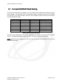
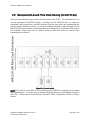
2.7 On-board ADC/DAC Clock Routing
The ADC clock distribution is handled by a set of external clock distribution buffers arranged
in two stages. The resulting clock from the two stages is selected by the FPGA using the
CLK_SEL[1:0]_[1:0] lines for stage 1 and CLK_SEL for stage 2 (refer to FPGA pin-out in VHDL
Sources release package).
‘0’
‘0’
‘0’
‘0’
‘1’
‘1’
‘1’
‘1’
CLK_SEL
CLK_SEL[1:0]_1
Don’t care
Don’t care
Don’t care
Don’t care
“00”
“01”
“10”
“11”
CLK_SEL[1:0]_0
“00”
“01”
“10”
“11”
Don’t care
Don’t care
Don’t care
Don’t care
Meaning
RTM Clock 0
On-Board 125MHz
(Reserved – clock off)
(Reserved – clock off)
Backplane TCLKA
RTM Clock 1
RTM Clock 2
Front CLK IN
Table 14: Selecting the ADC clock source
The DAC chip is clocked from the FPGA. Therefore it is flexible as to what clock is used to
drive it. The following diagram shows the ADC / DAC clock routing for the board.
NOTE: Higher resolution diagrams in PDF form can be found in the AMC520 VHDL Sources
distribution package.
VADATECH FORM No. 3WI731-01 Rev. B
VT-MAN-CUS-100402-2.2.1
Page 24 of 101
VadaTech AMC520 User’s Manual
Figure 9: On-board ADC/DAC Clock Routing
VADATECH FORM No. 3WI731-01 Rev. B
VT-MAN-CUS-100402-2.2.1
Page 25 of 101
VadaTech AMC520 User’s Manual
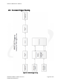
2.8 On-board Trigger Routing
Figure 10: On-board trigger routing
VADATECH FORM No. 3WI731-01 Rev. B
VT-MAN-CUS-100402-2.2.1
Page 26 of 101
VadaTech AMC520 User’s Manual
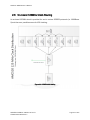
2.9 On-board QDRII+ / IODELAY Calibration / Misc Clocking
Two programmable oscillators are provided for driving the QDRII+ and other IODELAY
calibration / Misc clocking within the FPGA.
Figure 11: QDRII+, IODELAY calibration, and misc clock routing
2.10 Backplane/RTM Connections
Refer to the appendixes at the end of this document for backplane and RTM pin-outs.
VADATECH FORM No. 3WI731-01 Rev. B
VT-MAN-CUS-100402-2.2.1
Page 27 of 101
VadaTech AMC520 User’s Manual
2.1 FPGA Banking/Pinning/Floorplan
Detailed information on the FPGA Banking, Pinning, and Floorplan can be found in the
AMC520 VHDL Sources package in the ‘Docs’ directory.
2.2 FPGA SERDES Backplane Interfaces
The board is designed to support flexible system interfacing to the backplane via the
reprogrammable FPGA. Interfaces such as PCIe x1/x2/x4/x8 (Gen1 or Gen2), 1000Base-X,
Aurora, and others are realizable. The FPGA reference design demonstrates 1000Base-X to
AMC ports 0 & 1, PCIe x4 Gen 1 to AMC ports 4-7, and PCIe x4 Gen 1 to AMC Ports 8-11.
AMC Port
0
1
2
3
4
5
6
7
8
9
10
11
12
13
14
15
Reference Design
1000Base-X (hard core)
1000Base-X (hard core)
Connected but unused in reference design
Connected but unused in reference design
PCIe x4 Gen 1 Lane 0 (hard core)
PCIe x4 Gen 1 Lane 1 (hard core)
PCIe x4 Gen 1 Lane 2 (hard core)
PCIe x4 Gen 1 Lane 3 (hard core)
PCIe x4 Gen 1 Lane 0 (hard core)
PCIe x4 Gen 1 Lane 1 (hard core)
PCIe x4 Gen 1 Lane 2 (hard core)
PCIe x4 Gen 1 Lane 3 (hard core)
Connected but unused in reference design
Connected but unused in reference design
Connected but unused in reference design
Connected but unused in reference design
Table 15: FPGA reference design backplane SERDES interfaces
2.3 FPGA SERDES Front Panel Interfaces
The board is designed to support flexible system interfacing to the front panel SFP+ cages
via the reprogrammable FPGA. Interfaces such as 1000Base-X, Aurora, and others are
realizable. The FPGA reference design demonstrates 1000Base-X to SFP+ ports 0 & 1.
SFP+ Port
0
1
Reference Design
1000Base-X (hard core)
1000Base-X (hard core)
Table 16: FPGA reference design backplane SERDES interfaces
VADATECH FORM No. 3WI731-01 Rev. B
VT-MAN-CUS-100402-2.2.1
Page 28 of 101
VadaTech AMC520 User’s Manual
2.4 FPGA SERDES Reference Clocks
The AMC520 design attempts to provide the most flexible options for GTX clock forwarding
to enable a wide variety of SERDES protocols while minimizing the number of clocks on the
board to reduce noise to the ADCs.
Figure 12: Virtex 6 GTX clock forwarding for AMC520
VADATECH FORM No. 3WI731-01 Rev. B
VT-MAN-CUS-100402-2.2.1
Page 29 of 101
VadaTech AMC520 User’s Manual
2.5 Backplane/On-board PCIe Clock Routing (CLK3/FCLKA)
There are two different ways to clock the PCIe cores in the FPGA. The preferred way is to
use the backplane CLK3/FCLKA which is provided into the MGT115 bank, by using the
backplane clock coming from the MCH then the PCIe can work with both spread-spectrum
and non-spread-spectrum clocking. An on-board 100MHz oscillator is also provided into the
MGT114 bank which enables non-spread-spectrum clocking only if a backplane PCIe clock is
not available. Either clock can be used by either or both PCIe banks via internal clock
forwarding in the Virtex-6.
Figure 13: PCIe clock routing
NOTE: The FCLKA is used ONLY for PCIe clocking on the AMC520 in keeping with the latest
AMC specifications. It cannot carry an arbitrary CLK3 signal from the backplane through to
the FPGA. Please consult the VadaTech Telco/GPS Clock Configuration Guide for further
details.
VADATECH FORM No. 3WI731-01 Rev. B
VT-MAN-CUS-100402-2.2.1
Page 30 of 101
VadaTech AMC520 User’s Manual
2.6 On-board 125MHz Clock Routing
An on-board 125MHz clock is provided for use in various SERDES protocols (i.e. 1000BaseX) and also as a possible source for ADC clocking.
Figure 14: 125MHz clock routing
VADATECH FORM No. 3WI731-01 Rev. B
VT-MAN-CUS-100402-2.2.1
Page 31 of 101
VadaTech AMC520 User’s Manual
2.7 ADC Channel Coupling (Magnetic vs. OpAmp)
The 10-channel ADC channel coupling configuration can be ordered standard from the
factory as all Magnetic (F=0) or all OpAmp (F=1). However, some customers may find it
necessary to modify this coupling after purchase to either completely change from one type
to the other or to change only some channels from one type to the other.
WARNING: This section describes physical board modifications to be carried out at the
customer site. These modifications will void your warrantee if not performed by a skilled
electronics rework technician. The modifications are very simple since they only entail
moving some zero-ohm resistors, however, VadaTech will not be responsible for customercaused damage to the board.
The general location of the zero-ohm resistors is on the top (component) side of the board
as highlighted by the orange rectangles below:
Figure 15: ADC Coupling Zero-Ohm Resistors Location
Each channel is routed either to a magnetic or an op-amp circuit. This routing is done by
way of three-pad 0402 size zero-ohm resistors on the board. The center pad connects to
the ADC chip-side circuit and the other two outer pads connect to the magnetic or op-amp
circuits leading back to the RTM. Therefore, changing the coupling for the ADC chip is simply
a matter of shifting the zero-ohm resistors over on the pads using proper rework techniques.
VADATECH FORM No. 3WI731-01 Rev. B
VT-MAN-CUS-100402-2.2.1
Page 32 of 101
VadaTech AMC520 User’s Manual
There are connections for both the differential analog signals and the common mode. Both
must be matched for a proper configuration. Also, a single common mode signal comes
from each dual-channel ADC chip and is shared between two adjacent channels. Therefore
the coupling configuration must be changed in pairs and not individually.
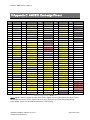
The following table lists the resistors which must be mounted for each coupling
configuration of each channel/pair of the AMC520 Rev C board:
ADC
Channel
0
1
2
3
4
5
6
7
8
9
Channel
Pair
A
B
C
D
E
Magnetic
OpAmp
R937/R936/R44
R934/R933/R44
R685/R684/R11
R682/R681/R11
R661/R660/R7
R664/R663/R7
R639/R638/R3
R33/R477/R3
R94/R645/R5
R644/R640/R5
R940/R935/R78
R939/R932/R78
R688/R683/R12
R686/R680/R12
R665/R659/R8
R667/R662/R8
R641/R634/R4
R491/R490/R4
R647/R584/R6
R646/R635/R6
Table 17: ADC Channel Coupling Resistors
Two example diagrams are shown below. The first diagram shows where the three-pad
resistors should be mounted to make channels 0 and 1 use Magnetic coupling. The second
diagram shows where the three-pad resistors should be mounted to use OpAmp coupling.
The other pairs of channels follow a very similar layout to these example channels.
Figure 16: ADC Channel Coupling: Channels 0/1 Magnetic Example
Figure 17: ADC Channel Coupling: Channels 0/1 OpAmp Example
VADATECH FORM No. 3WI731-01 Rev. B
VT-MAN-CUS-100402-2.2.1
Page 33 of 101
VadaTech AMC520 User’s Manual
3 IPMI MMC Serial Menu Interface
The IPMI MMC microcontroller handles communication with the AMC carrier and must
provide E-Keying information to describe the SERDES ports used on the AMC card-edge
connector. The MMC configuration for E-Keying initially ships with a matching set of EKeying records for the FPGA reference design, meaning two GbE ports on AMC Ports 0 & 1,
PCIe on AMC ports 4-7, and XAUI ports on AMC Ports 8-11. If you change the FPGA design to
use different ports or protocols then you should use the MMC controller’s menu system to
configure the appropriate e-keying records. Using incorrect E-Keying records can result in
unexpected behavior.
The interface to the MMC is via the IPMI RS-232 port (refer to the hardware overview section
for more information). The port settings are 115200-8-N-1-NOFLOW. The configuration is
described in the following sections.
3.1 E-Keying Configuration
Electronic Keying or E-Keying is a complex subject that is beyond the scope of this
document. The rest of this section assumes familiarity with the relevant sections of
PICMG® AMC.0 R2.0 Advanced Mezzanine Card Base Specification and the AMC.1, AMC.2
and AMC.3 subsidiary specifications.
The FPGA on the AMC can be programmed to support multiple link types in the Common
Options region and the Fat Pipes Region of the connector. In order for the AMC to function
properly in a MicroTCA or ATCA carrier, the AMC’s FRU Information must correctly describe
the link types provided by the FPGA. To set the E-Keying information, type ekey and press
Enter. This will display a list of common link descriptors. Any link descriptor can be enabled
or disabled by typing the corresponding number and pressing Enter. When the configuration
is correct, type “save” and press Enter to save it in the AMC’s FRU Information. To cancel
your changes and return to the main menu, type “cancel” and press Enter.
VADATECH FORM No. 3WI731-01 Rev. B
VT-MAN-CUS-100402-2.2.1
Page 34 of 101
VadaTech AMC520 User’s Manual
4 IPMI Sensors
The AMC520 Management Controller monitors the following sensors:
Sensor Number
0x90
0x10
0x11
0x18
0x19
0x20
0x28
0x29
Name
VT AMC520 HS
VT AMC520 T1
VT AMC520 T2
VT AMC520 Tint
VT AMC520 Text
VT AMC520 12V
1.0V
1.5V
Description
AMC.0 Hot-Swap Sensor
Intake Air Temperature
Exhaust Air Temperature
Board Temperature near FPGA
FPGA Die Temperature
12V Input Power
1 Volt Rail Voltage
1.5 Volt Rail Voltage
Table 18: MMC Sensors
To access the sensors please refer to your AMC carrier’s documentation.
VADATECH FORM No. 3WI731-01 Rev. B
VT-MAN-CUS-100402-2.2.1
Page 35 of 101
VadaTech AMC520 User’s Manual
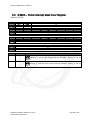
5 FPGA Reference Design
The FPGA is fully customizable and it is expected that the customer will need to provide their
own custom FPGA design to enable application-specific data processing within the fabric.
However, a reference design is provided to demonstrate the basic board hardware
functionality and to act as a manufacturing/ acceptance test.
5.1 FPGA Reference Design External Interfaces
The reference design demonstrates the following ports:
2 – 1000Base-X Ethernet to AMC Ports 0 & 1 (link only, no traffic)
2 – 1000Base-X Ethernet to SFP+ Ports 0 & 1 (link only, no traffic)
PCIe x4 Gen 1 to AMC Ports 4-7 (full register interface)
PCIe x4 Gen 1 to AMC Ports 8-11 (configuration space only)
10-channels (5 chips) of ADC w/ BIST verifier and data path and synchronizer
2-channels (1 chip) of DAC w/ built-in signal generation
QDRII+ 72-bit SRAM controller
4 - User LEDs w/ diagnostic display
16 - Status LEDs w/ diagnostic display
Clock/trigger routing interfaces
SYSMON temperature/voltage readings
FPGA RS-232 port (loopback)
16 - User I/O Outputs
MRT520 DensiShield external loopback test for RTM data/clock interfaces
NOTE: These are the interfaces chosen for the reference design, but the FPGA’s pin-out is
designed to enable a great deal of flexibility for customer-specific applications. Many
different styles of interfaces are possible to both the AMC backplane and front panel
through custom FPGA development at the customer’s site.
VADATECH FORM No. 3WI731-01 Rev. B
VT-MAN-CUS-100402-2.2.1
Page 36 of 101
VadaTech AMC520 User’s Manual
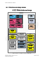
5.2 FPGA Reference Design Internals
Figure 18: AMC520 FPGA Top-Level Reference Design Diagram
VADATECH FORM No. 3WI731-01 Rev. B
VT-MAN-CUS-100402-2.2.1
Page 37 of 101
VadaTech AMC520 User’s Manual
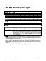
AMC520 FPGA ADC Reference Design Pipeline (High-speed ADC Snapshot Capture)
Dual-Clock FIFO
(minimal)
Data
(16 bit)
Data
(16 bit)
Data
(16 bit)
PCIe 125MHz Transaction Domain
Data
(32 bit)
PCIe Bridge Read
Dual-Clock FIFO
(large for storage)
Single Channel Selector
(10:1)
Data
(16 bit)
CPU BAR 4 Register
(Four more identical chips;
Total 5 chips / 10 channels
Each chip its own bank / Regional Clock domain)
SNAPSHOT STORAGE AVAILABLE:
~128 Kilo-samples
DISCLAIMER: It is assumed that an end-user design is likely to perform DSP to
intelligently reduce the data and/or streaming operations to extend the sampling time
(typically to support continuous sampling), but that is beyond the scope of this example
design. The example design captures a snapshot in one pass and then the snapshot
is read by the CPU in another pass for the purpose of creating a raw data file for
analysis. The limitations of the example design are not intended to be nor should be
considered as limitations to the end-user design.
pcie_local_bridge.vhd
CLK
adc_selector.vhd
DCO
BUFR
IDELAY
(fixed minimum delay to
match data path intrinsic
delay)
DIFF DCO
IBUFDS
(LVDS DIFF_TERM)
CLK
adc_chip.vhd
DATA B
(17 bit SDR)
Data
(16 bit)
Dual-Clock FIFO
(minimal)
IDDR x 17
(1:2)
(16-bit data + OR bit)
ADC 125 MHz SDR Global Domain
adc_chan.vhd
DATA A
(17 bit SDR)
adc_chan.vhd
DATA
(17 bit DDR)
BIST Verifier/Data Passthrough
(Strips OR bit)
ADC 125 MHz SDR/Non-interleaved Domain
BIST Verifier/Data Passthrough
(Strips OR bit)
IDELAY x 17
DIFF DATA
(17 bit DDR)
IBUFDS x 17
(LVDS DIFF_TERM)
ADC 125 MHz DDR/Interleaved Domain
NOTE: Transfer of a single
ADC channel at a time is
supported by the reference
design for sake of simplicity.
Figure 19: AMC520 FPGA ADC Reference Design Diagram
VADATECH FORM No. 3WI731-01 Rev. B
VT-MAN-CUS-100402-2.2.1
Page 38 of 101
VadaTech AMC520 User’s Manual
AMC520 FPGA DAC Reference Design Pipeline
(Continuous Looping DAC Output)
DATA B
(16 bit SDR)
SINE/RAMP
Data Gen
dac_chan.vhd
dac_chan.vhd
DATA B
(17 bit SDR)
DATA A
(16 bit SDR)
SINE/RAMP
Data Gen
OSERDES x 14
(2:1 SDR->SDR)
DATA
(18 bit SDR)
dac_chip.vhd
ODELAY x 18
DIFF DATA
(18 bit SDR)
OBUFDS x 18
(LVDS)
DATA A
(17 bit SDR)
XOR Generator
“1010” Clock
Pattern
XOR Generator
DAC_CLK0
(Fs * 2)
DAC 250 MHz SDR/Non-Interleaved Domain
OSERDES x 14
(4:1 SDR->DDR)
ODELAY
DIFF DAC_CLK0
(Fs * 2)
OBUFDS
(LVDS)
DAC 500 MHz SDR/Interleaved Domain
Five looping
data patterns
are available:
SINE Fs/2
SINE Fs/4
SINE Fs/8
SINE Fs/16
RAMP
“10” SELIQ Fixed Pattern
(2 x 1 bit SDR)
Figure 20: AMC520 FPGA DAC Reference Design Diagram
NOTE: Full-size versions of these diagrams are available in the AMC520 VHDL Sources
package under the ‘Docs’ directory.
In addition to the Xilinx SERDES/MIG cores which make up some of the external interfaces
in the reference design, there are various other VadaTech cores in the design which are
described below.
5.2.1 PCIe Bridge (pcie_local_bridge.vhd)
The PCIe Bridge implements a state machine which converts PCIe Transaction layer packets
into internal register bus transactions. It supports up to 32-bit PIO reads and up to 32-bit
PIO writes. Byte enables are supported for register accesses so individual bytes may be
read/written if desired.
The PCIe bridge also includes a state machine for handling in-band interrupt signaling to the
host processor.
VADATECH FORM No. 3WI731-01 Rev. B
VT-MAN-CUS-100402-2.2.1
Page 39 of 101
VadaTech AMC520 User’s Manual
5.2.2 Interrupt Controller (vt_interrupt_controller_x32.vhd)
The interrupt controller consolidates the level-sensitive interrupt lines coming from several
internal and external sources to provide one single master interrupt line to the PCIe Bridge.
The interrupt controller also supports a Bit Change Interrupts which are effectively edge
detectors combined with an event capture mechanism used for alerting the software any
time monitored lines such as the thermal alert line change state.
5.2.3 Clock Router (clock_router.vhd)
The Clock Router enables flexible routing of off-board and on-board clocks. It also
enables/disables various input/output buffers. See the register specification that follows for
details of routing sources and targets.
5.2.4 LED Controller (leds.vhd)
The LED Controller allows various statuses to be reflected onto the front panel User LEDs.
Refer to the Hardware Overview section for status information displayed.
5.2.5 ADC Chip Controller (adc_chip.vhd)
This core controls one instance of a dual-channel ADC chip and includes instances of the
two ADC channels which the chip handles in addition to an instance of a SPI Master
controller to facilitate communication to ADC chip registers. This core includes the basic
source-synchronous clocking and I/O interfacing for the ADC chip interface to the FPGA. It
includes the ability to delay the data relative to the clock if needed.
5.2.6 ADC Channel (adc_chan.vhd)
This core implements a single de-interleaved ADC channel with a BIST verify and data
channel which connects to the ADC Selector.
5.2.7 ADC SPI Master (adc_spi.vhd)
This core implements a SPI Master for communicating with the ADC chip registers.
VADATECH FORM No. 3WI731-01 Rev. B
VT-MAN-CUS-100402-2.2.1
Page 40 of 101
VadaTech AMC520 User’s Manual
5.2.8 ADC Synchronizer (adc_sync.vhd)
This core outputs synchronization pulses to the five ADC chips on the board so that when
they are in a divided down clock mode they will all sample coherently on the same clock
edge. This core includes the ability to delay the sync pulses relative to the ADC global clock
if necessary. NOTE: Although the FPGA provides this example of how to generate sync
pulses, the reference design doesn’t use the ADC chips in a divided down mode so the
effect of the sync pulse generation is only visible by probing the signals on the board or if the
customer sets up their own divided down mode for the ADC chips.
5.2.9 ADC Selector (adc_selector.vhd)
This core picks off the data from one of the ten ADC channels and stores it into one large
storage FIFO. This storage FIFO can then be read out by the external CPU via PCIe to collect
ADC sample data into a file.
5.2.10 DAC Chip Controller (dac_chip.vhd)
This core controls the dual-channel DAC chip and includes two instances of the DAC
channels the chip handles. This core includes the basic source-synchronous clocking and
I/O interfacing for the DAC chip interface to the FPGA. It includes the ability to delay the
data relative to the clock if needed.
5.2.11 DAC Channel (dac_channel.vhd)
This core implements a DAC channel with data generation for nine different looping data
patterns: All zeros, All ones, All mid-level, Ramp, SINE Fs/2, SINE Fs/4, SINE Fs/8, and SINE
Fs/16, or a user supplied level. The sine patterns generate continuous sine waves but only
utilize a limited number of DAC symbols. The ramp pattern generates every DAC symbol
from 0x0000 through 0xFFFF and then wraps around and repeats (creating a saw-tooth
wave).
In addition to the data generation capabilities, the DAC channel cores can also loop-through
the ADC data from any of the 10 ADC channels such that the analog output will be a
reproduction of the analog input.
5.2.12 BPI Flash Core (bpi_flash.vhd)
A BPI Flash core is present which enables access to the BPI Flash on the board via PCIe.
This core enables the software running on the host CPU to reprogram the FPGA
configuration file and trigger re-configuration. The software has a feature which enables this
VADATECH FORM No. 3WI731-01 Rev. B
VT-MAN-CUS-100402-2.2.1
Page 41 of 101
VadaTech AMC520 User’s Manual
to be seamless by saving off and then restoring the PCIe core configuration info across the
reconfiguration of the FPGA.
5.2.13 SYSMON Core (sysmon_core.vhd)
A SYSMON core is present which captures the internal die temperature, internal voltage, and
auxiliary voltage.
5.2.14 Utility Core (vt_utility_x32.vhd)
A utility cores is present which contains read-only identification information such as version,
signature, etc. It also contains some read-only registers which reflect current status
information that can change over time. There is also a scratch register present in this core
which is useful for bus testing.
5.2.15 Miscellaneous Helper Cores
Some general-purpose VadaTech cores, which were not described previously, are also
included in the reference design as follows:
General Purpose Arbitrary Clock Enable Divider (vt_clocken_div_arbitrary.vhd)
o Provides a re-usable way to slow down portions of the design while still using
the same clock
General Purpose Reset Synchronizer (vt_reset_sync.vhd)
o Provides a re-usable asynchronous assertion/synchronous de-assertion reset
General Purpose Clock Synchronizer (vt_multi_sync.vhd)
o Provides a re-usable clock domain crossing for individual signals to help
mitigate meta-stability
5.2.16 Xilinx IP Cores
The following cores from Xilinx are used:
Virtex-6 Integrated Block for PCI Express (x2)
o Wraps the two Virtex-6 embedded PCIe cores
o Provides the basic control/status/data interface for the reference design
o Provides for basic backplane verification for PCIe
VADATECH FORM No. 3WI731-01 Rev. B
VT-MAN-CUS-100402-2.2.1
Page 42 of 101
VadaTech AMC520 User’s Manual
Virtex-6 Embedded Tri-mode Ethernet MAC Wrapper (x2)
o Wraps the four Virtex-6 embedded MAC cores and GTX transceivers
o Used in 1000Base-X mode in this design for backplane/SFP+ verification
Memory Interface Generator
o Used to generate a QDRII+ 72-bit memory controller
o Includes built-in BIST engine
FIFO Interface Generator
o Used for various clock domain crossing and data storage purposes
VADATECH FORM No. 3WI731-01 Rev. B
VT-MAN-CUS-100402-2.2.1
Page 43 of 101
VadaTech AMC520 User’s Manual
6 Customer FPGA Development
The reference FPGA design combines IP cores from Xilinx with VadaTech custom VHDL code.
This design can be changed or replaced by the customer to allow for custom DSP/control
solutions that are tailor-made to take full advantage of the Xilinx Virtex-6 FPGA.
It is expected that if the customer wishes to synthesize a new FPGA image, that they will
have access to both Xilinx ISE v13.4 (full version required to support the Virtex-6 chip on the
board) as well as the necessary IP cores. Xilinx may require per-core licenses even if they
are free. The Xilinx ISE tool license and core licenses are NOT included as part of the
purchase of the AMC520 card.
LEGAL NOTICE: The VadaTech custom VHDL code included in this reference design is the
intellectual property of VadaTech Incorporated. Permission is granted to use the VadaTech
custom VHDL code royalty-free in customer designs targeting the VadaTech AMC520 card
only. Redistribution to third parties or use of this code for any other purpose is strictly
prohibited. VadaTech is not responsible for damage or loss caused by reprogramming of the
FPGA by the customer. Use caution when changing the reference design or creating your
own design as it is possible to damage components on the AMC520 board or other attached
boards/equipment.
If a completely new design is desired it is recommended that at a minimum the UCF files
from the reference design be used since they provide the complete pin-out of the FPGA on
the AMC520 board. The provided source files were used to create the flash image that is
shipped on the board from VadaTech.
VADATECH FORM No. 3WI731-01 Rev. B
VT-MAN-CUS-100402-2.2.1
Page 44 of 101
VadaTech AMC520 User’s Manual
6.1 Modular FPGA Project Design
The FPGA reference design uses a modular and flexible design for supporting multiple
densities, speed grades, and control interfaces. Each unique combination of these variables
is wrapped into an ISE project for the combinations that are currently supported (contact
VadaTech if your desired combination is not listed). The following table shows how the
projects use the available high-level modules to create unique supported product variations:
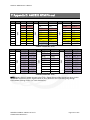
AMC520-XXX-42X-1XX
High-Level Module
amc520_fpga_low_density.ucf
amc520_fpga_amc_pcie_2x4.vhd
X
X
Table 19: Modular FPGA Project Variations
When reviewing the VHDL sources it is important to understand the thinking behind the
project layout. In the root of the project folder you will find the VadaTech-developed VHDL
source files. In this directory you will also find an amc520_fpga_coregen.xise project file
which is used to generate all of the Xilinx IP cores into the ipcore_dir directory. The
contents of this directory include only the Xilinx generated files without modification. The
coregen project is not used to create an actual FPGA image, it is only used to create
common Xilinx IP cores for use by the targeted sub-projects.
Sometimes it is necessary for VadaTech to modify the Xilinx generated files for special
situations such as re-arranging clocking resources or to flip polarity of a SERDES pair, etc.
When these situations arise we create a new directory with a prefix of Customized_ (such as
Customized_1000BaseX) where we will copy ONLY the Xilinx generated files that need direct
modification and we make the changes in this location. This ensures that the
customizations are not lost if the cores are regenerated. However, if/when the cores are
regenerated and the parameters to the core are changed, you will need to perform a threeway merge between the newly generated IP files in the sub-directories of ipcore_dir and
the Customized_* directories. This three-way merge needs to ensure that the newly
generated options are incorporated while simultaneously preserving the VadaTech
customizations. When regenerating IP with different parameters please also ensure that the
changes are updated to the amc520_lib.vhd file too since various generics are listed in this
file and will take precedence over the files in ipcore_dir.
Finally, a sub-directory containing the ordering options of the board is present (such as
AMC520_XXX_42X_1XX) which includes the actual project file used to generate the FPGA
images for the named board configuration by combining the appropriate source files in the
root, Customized_* sub-directories, and ipcore_dir sub-directories.
VADATECH FORM No. 3WI731-01 Rev. B
VT-MAN-CUS-100402-2.2.1
Page 45 of 101
VadaTech AMC520 User’s Manual
6.2 FPGA Development/Debug Cycle
During FPGA development various different programming mechanisms are supported:
1) Configure FPGA directly via front panel or backplane JTAG using Xilinx Impact or
equivalent and a .bit file. Remember to set the JTAG front/back switch setting on the board.
The configuration remains only during the current power-up. No PCIe activity should be
taking place to the AMC520 while the FPGA is reconfigured or the host CPU could lock-up,
crash, etc. If this configuration is done after the host CPU’s operating system has configured
the PCIe BARs then it will be necessary to reboot the host CPU before attempting to use the
PCIe bus to the AMC520. This will cause the host CPU to rescan the PCIe bus and configure
the BARs appropriately.
2) Program FPGA’s BPI Flash via front panel or backplane JTAG using Xilinx Impact or
equivalent using a .mcs file. Remember to set the JTAG front/back switch setting on the
board. Then reset/power-cycle the board to have the FPGA configure itself from the BPI
flash. The configuration remains permanent and will take effect at every power-up. No PCIe
activity should be taking place to the AMC520 while the FPGA’s BPI flash is reprogrammed
or the host CPU could lock-up, crash, etc. While programming the BPI flash the Xilinx Impact
tool downloads its own FPGA core in order to facilitate programming and during this time the
PCIe link to the AMC520 will go down.
3) Program the FPGA’s BPI Flash via PCIe using the amc520tool and
amc520_fpga.ko driver provided using a .bin file. During this process the PCIe configuration
data that the operating system originally setup will be preserved, then the BPI flash
programmed, then the FPGA will be instructed to reconfigure itself from the BPI flash, and
finally the PCIe configuration data will be restored into the FPGA’s PCIe core. The new FPGA
image can then seamlessly be used without the need to reboot the host CPU. The
configuration remains permanent and will take effect at every power-up.
NOTE: Approach #3 is only valid if the PCIe core’s configuration space has not been modified
in the new FPGA image compared to the one that is running at the time of the reprogramming. If PCIe BARs are being added or resized, etc the safest thing to do is use
approach #2 or alternatively the customer could create a variation of this scheme in the
software that simply programs the BPI flash and then reboots the host CPU without
attempting to restore the previous state. Attempting to restore the previous PCIe
configuration state into an FPGA PCIe core that has been re-structured may result in the host
CPU locking up, crashing, etc.
The .bin and .bit files can be created via Xilinx ISE; the reference design project is setup to
create both.
The .mcs file can be created by encapsulating a .bit file using Xilinx Impact; the reference
design project is setup to do this as well.
VADATECH FORM No. 3WI731-01 Rev. B
VT-MAN-CUS-100402-2.2.1
Page 46 of 101
VadaTech AMC520 User’s Manual
7 Host-side Software Support
The AMC520 board includes access to a software tool and device driver which are used to
control the FPGA reference design from an external PCIe Host CPU (not included) such as an
x86 PrAMC or desktop PC w/ VadaTech PCI101 adapter. The software support includes the
following:
amc520_fpga.ko: Device driver module to control the FPGA via PCIe
amc520tool: Tool for controlling the device driver/FPGA
Sources are made available for the device driver and tool so that they can be used as an
example for your own application-specific designs.
NOTE: Due to the complete re-programmability of the FPGA, it is not possible to make a
universal AMC520 device driver/tool application. The driver/tool provided matches the
FPGA image provided as the reference design. If the FPGA image is replaced or changed by
the customer then it follows that the customer will also need to update the device
driver/tool appropriately.
7.1 AMC520 Device Driver
To compile the AMC520 device driver:
1) Enter the driver directory
2) Modify the Makefile if necessary to point to your Linux kernel source directory
3) Type make
The device driver is loaded by issuing the following command:
insmod /modules/amc520_fpga.ko
The device driver supports open, close, poll/select, and ioctl operations from the application.
Generally the application should open() the device, then make an ioctl call to get
information about the device if desired.
The application can then use ioctls to setup the FPGA as desired. Then it can call the
poll() or select() system call to wait for status changes to become available. The
application can use POLLPRI to watch for status changes (POLLIN is reserved for future use
by customer applications which may need data collection notification, etc). If the driver
indicates that the status changed then the application should read the status using the
appropriate ioctl.
Once the application is done with the card it should close() the file handle.
VADATECH FORM No. 3WI731-01 Rev. B
VT-MAN-CUS-100402-2.2.1
Page 47 of 101
VadaTech AMC520 User’s Manual
The ioctl() interfaces available for the device driver are documented in an appendix at the
end of this document. These interfaces are the primary means for controlling and getting
status from the FPGA reference design. The amc520tool application utilizes these ioctls.
7.2 AMC520 Tool Application
The amc520tool provides basic support for controlling the FPGA and gathering status via the
amc520_fpga.ko driver interfaces. It also supports various diagnostic tests.
To compile the tool application:
1) Enter the tool directory
2) Type make
The usage information for the tool is shown below:
AMC520 Tool v2.0.2 R1
usage: amc520tool <cmd> [<opts>]
LOW-LEVEL DEBUG CMDs:
sig_test
- Repeated read test
scratch_test
- Repeated read/write test
useriotest [0/1]
- Show/set Front User I/O test mode
rtmtest [0/1]
- Show/set RTM Data/Clock LB test mode
readreg <addr>
- Read BAR 4 PCIe register
writereg <addr> <val>
- Write BAR 4 PCIe register
dumpreg ['all']
- Dump BAR 4 PCIe contents
readexreg <addr>
- Read BAR 5 PCIe register
writeexreg <addr> <val> - Write BAR 5 PCIe register
dumpadc <chip>
- Dump ADC chip SPI registers
readadc <chip> <addr>
- Read ADC chip SPI register byte
writeadc <chip> <addr> <value>
- Write ADC chip SPI register byte
bpi_id
- Report the FPGA BPI flash mfg/dev IDs
bpi_dump [all]
- Dump the FPGA BPI flash contents
bcistatus
- Wait for FPGA monitored status
adcdelay <chip> [<tap>] - Show/set ADC delay(chip=0-4, tap=0-31)
dacdelay [<tap>]
- Show/set DAC delay (tap=0-31)
syncdelay [<tap>]
- Show/set SYNC delay (tap=0-31)
PRIMARY CMDs:
detect
- Detect driver/FPGA versions
portstatus ['refresh']
- Show FPGA backplane/SFP+ port statuses
sysmon
- Report system monitor info
bpi_program <bin_file>
- Program the FPGA BPI flash
dac [<xor_en> <chan0_mode> <chan1_mode>]
chanX_mode=run_zeros|run_ones|run_mid|run_ramp|run_fsdiv2|
run_fsdiv4|run_fsdiv8|run_fsdiv16|(fixed value)|
run_adc<0-9>|stop
- Show/set DAC mode
routing [<target> <src>] - Show/Set FPGA clock routing target's source
target: tclka, tclkb, tclkc, tclkd, trigstart, trigend, trigout
src:
disable, zero, one, tclka, tclkb, tclkc, tclkd, trigstart,
trigend, trigin, dactoggle, adcclk, adc0toggle, adc1toggle,
adc2toggle, adc3toggle, adc4toggle
VADATECH FORM No. 3WI731-01 Rev. B
VT-MAN-CUS-100402-2.2.1
Page 48 of 101
VadaTech AMC520 User’s Manual
adcclksel [<sel>]
sel:
- Show/Set ADC clock selector
rtmclk0, rtmclk1, rtmclk2, 125mhz, tclka, front
sync [<div>]
- Show/set ADC sync (div 0=OFF, 1=DIV2, ...)
adc <chan> <run_adc_analog|
- ADC analog samples
run_adc_midscale| - ADC fixed mid-scale
run_adc_posfull|
- ADC fixed +full-scale
run_adc_negfull|
- ADC fixed -full-scale
run_adc_checker|
- ADC checkerboard
run_adc_pnlong|
- ADC PRN long seq
run_adc_pnshort|
- ADC PRN short seq
run_adc_toggle|
- ADC toggle seq
run_ramp|
- FPGA ramp pattern
bist>
- Auto-BIST w/ ADC checkerboard
- Operate an ADC channel with the given mode
NOTE: The stdout from this command is BINARY and should be redirected
to a file or alternatively to a pipe such as netcat for
direct transmission to another system. Only one ADC channel
should be running at a time for this reference design.
adccheck <filename>
adcconv <filename>
- Check file for ADC overflow
- Convert binary file to CSV on stdout
The options for the tool generally follow the field definitions in the register specification.
Please refer to the register specification later in the document for details. The
amc520_fpga.ko driver module must be loaded prior to using the tool.
ADC Example (capturing channel 0 with on-board 125MHz clock):
The manual way of capturing data is shown below (a simpler way is shown following):
./amc520tool adc 0 run_adc_analog > /tmp/chan0.bin
./amc520tool adccheck /tmp/chan0.bin
./amc520tool adcconv /tmp/chan0.bin > /tmp/chan0.csv
(optional)
The above example runs the ADC channel 0 and collects the snapshot data into a binary file.
Then the binary file is optionally checked for overflow, etc. Finally the binary file is converted
into a comma separated values file. Either file can be loaded into Matlab or some other
analysis tool as desired. All ten channels can be checked one at a time.
A script called capture is provided to simplify the process shown above, so it can be
condensed as:
./capture 0
(outputs to chanX.bin and chanX.csv)
Another helper script called capture_all is provided which allows interactive capture of all
10 channels. The script prompts the user to press enter before each channel’s data is
captured so that the signal generation equipment may be setup, etc.
./capture_all
VADATECH FORM No. 3WI731-01 Rev. B
VT-MAN-CUS-100402-2.2.1
(outputs to chan<0‐9>.bin and chan<0‐9>.csv)
Page 49 of 101
VadaTech AMC520 User’s Manual
DAC Examples:
amc520tool dac 1 run_fsdiv16 run_fsdiv16
The above example runs the DAC using XOR data mode with both channel 0 and channel 1
outputting a sine wave with frequency Fs/16.
amc520tool dac 1 run_adc3 run_adc4
The above example runs the DAC using XOR data mode with both channel DAC channel 0
outputting ADC channel 3’s data and DAC channel 1 outputting ADC channel 4’s data. This
demonstrates the ADC-to-DAC loop-through feature.
Ethernet/PCIe Status Example:
amc520tool portstatus refresh
The above example shows the status of the SERDES ports on the FPGA including the two
1000Base-X ports to the AMC Ports 0 & 1, two PCIe x4 ports to AMC Ports 4-7 and 8-11, and
two 1000Base-X ports to the front SFP+ ports. Press CTRL-C to exit the refresh loop.
Clock Routing Example:
amc520tool
amc520tool
amc520tool
amc520tool
amc520tool
amc520tool
amc520tool
routing
routing
routing
routing
routing
routing
routing
tclka dactoggle
tclkb dactoggle
tclkc dactoggle
tclkd dactoggle
trigstart dactoggle
trigend dactoggle
trigout dactoggle
The example above sends the ‘dactoggle’ signal (DAC clock divided by 2) to the four
backplane TCLK M-LVDS channels, the two backplane M-LVDS trigger channels, and the
front panel TRIG OUT connector.
NOTE: The DAC clock in this reference design is 125MHz resulting in a toggle signal of
62.5MHz.
VADATECH FORM No. 3WI731-01 Rev. B
VT-MAN-CUS-100402-2.2.1
Page 50 of 101
VadaTech AMC520 User’s Manual
8 Appendix A: FPGA PCIe Register Specification
The reference design’s register space is controlled by an external CPU via PCIe x4 on AMC
Ports 4-7. An external CPU may also connect via PCIe x4 on AMC Ports 8-11 however this
port supports only link establishment and OS configuration but not internal registers.
8.1 FPGA Reference Design PCIe Config Space
The PCIe configuration space as seen by the external CPU attached to either AMC Ports 4-7
or AMC Ports 8-11:
Item
Vendor ID
Device ID
Subsystem Vendor ID
Subsystem Device ID
Value
0xABCD (VadaTech Incorporated)
0x4520 (AMC520)
0xABCD (VadaTech Incorporated)
0x4520 (AMC520)
Table 20: FPGA reference design PCIe device/vendor IDs
BAR
4
5
Size
64 KB
8 MB
Type
32-bit addr MMIO
32-bit addr MMIO
Access Style
32-bit PIO w/ byte enables
32-bit PIO w/ byte enables
Contents
Internal registers
(for customer expansion)
Table 21: FPGA reference design PCIe BAR configuration
The design supports a control/status register interface via BAR 4 using 32-bit PIO access to
the internal registers.
The BAR 4 registers utilize a simple internal bus mechanism to interface to the PCIe Local
Bridge core. This mechanism expects that read data is already available, and the local
bridge will issue a read completion pulse once it is captured by the bridge (to facilitate
popping a ‘first word fall through’ style FIFO for example). Write data is provided
simultaneously with a write pulse, and the internal registers are expected to absorb the write
data as fast as the local bridge can provide it. There is no flow control mechanism for the
BAR 4 registers.
The BAR 5 registers utilize a handshaking mechanism intended to provide some means of
flow control. This mechanism provides a single-clock read request pulse simultaneous with
the address and then waits for a read acknowledge pulse. The read data is captured by the
local bridge on the first clock cycle on which the read acknowledge pulse is seen by it. The
read request will time-out after 10 clock cycles and will be abandoned if no
acknowledgement is seen. This prevents lock-up of the PCIe bus. Write data is provided
simultaneously with a write pulse, and the internal registers are expected to absorb the write
data as fast as the local bridge can provide it. Therefore, there is a flow control mechanism
for BAR 5 reads but not for writes.
VADATECH FORM No. 3WI731-01 Rev. B
VT-MAN-CUS-100402-2.2.1
Page 51 of 101
VadaTech AMC520 User’s Manual
NOTE: These BAR 4 & 5 access styles are provided simply as a reference. If your application
requires a different access style, then please feel free to customize them to suit your needs.
The goal of these mechanisms is simplicity and NOT performance. The PCIe interface can
perform at greater efficiency if you design your registers/FIFOs to support PCIe pipelining
and/or DMA operations. This is beyond the scope of the VadaTech reference design.
The design includes an interrupt controller which signals interrupts using either Legacy INTA
or an MSI vector.
Refer to the register specification in a subsequent section for details of the internal registers
BAR.
As mentioned previously, only the AMC Ports 4-7 PCIe actually has internal registers
attached. The AMC Ports 8-11 PCIe is an exact clone of the first port but there are no
internal registers attached to it. This second port is provided simply to verify the low-level
hardware connectivity.
The register map and detailed register specification for AMC Ports 4-7 PCIe are shown on
the following pages.
VADATECH FORM No. 3WI731-01 Rev. B
VT-MAN-CUS-100402-2.2.1
Page 52 of 101
VadaTech AMC520 User’s Manual
Core
Interrupt
Controller
BPI Flash
Controller
Clock Router
DAC
ADC Chip 0
ADC Chip 1
ADC Chip 2
ADC Chip 3
BAR4 Offset
0x0000
0x0004
0x0008
0x000C
0x0010 – 0x00FF
0x0100
0x0104
0x0108
0x010C – 0x07FF
0x0800
0x0804
0x0808
0x080C
0x0810
0x0814
0x0818
0x081C
0x0820 – 0x0FFF
0x1000
0x1004
0x1008
0x100C – 0x1FFF
0x2000
0x2004
0x2008
0x200C
0x2010
0x2014 – 0x27FF
0x2800
0x2804
0x2808
0x280C
0x2810
0x2814 – 0x2FFF
0x3000
0x3004
0x3008
0x300C
0x3010
0x3014 – 0x37FF
0x3800
0x3804
0x3808
0x380C
0x3810
0x3814 – 0x3FFF
Mnemonic
GIMSR
GIMCR
GISR
BCSR
N/A
BPICTRL
BPIADDR
BPIDATA
N/A
CREN
CRTCLKA
CRTCLKB
CRTCLKC
CRTCLKD
CRTRIGSTART
CRTRIGEND
CRTRIGOUT
N/A
DACCTRL
DACDELAY
DACFD
N/A
ADCCTRL0
ADCDELAY0
ADCBIST00
ADCBIST10
SPICTRL0
N/A
ADCCTRL1
ADCDELAY1
ADCBIST01
ADCBIST11
SPICTRL1
N/A
ADCCTRL2
ADCDELAY2
ADCBIST02
ADCBIST12
SPICTRL2
N/A
ADCCTRL3
ADCDELAY3
ADCBIST03
ADCBIST13
SPICTRL3
N/A
Description
Global Interrupt Mask Set Register
Global Interrupt Mask Clear Register
Global Interrupt Status Register
Bit-Change Status Register
Reserved
BPI Flash Control Register
BPI Flash Address Register
BPI Flash Data Register
Reserved
Clock Router Enables Register
Clock Router TCLKA Source Register
Clock Router TCLKB Source Register
Clock Router TCLKC Source Register
Clock Router TCLKD Source Register
Clock Router Trig Start Source Register
Clock Router Trig End Source Register
Clock Router TRIG OUT Source Register
Reserved
DAC Control Register
DAC Delay Register
DAC Fixed Data Register
Reserved
ADC Chip 0 Control Register
ADC Chip 0 Delay Register
ADC Chip 0 BIST 0 Register
ADC Chip 0 BIST 1 Register
ADC Chip 0 SPI Control Register
Rsvd
ADC Chip 1 Control Register
ADC Chip 1 Delay Register
ADC Chip 1 BIST 0 Register
ADC Chip 1 BIST 1 Register
ADC Chip 1 SPI Control Register
Rsvd
ADC Chip 2 Control Register
ADC Chip 2 Delay Register
ADC Chip 2 BIST 0 Register
ADC Chip 2 BIST 1 Register
ADC Chip 2 SPI Control Register
Rsvd
ADC Chip 3 Control Register
ADC Chip 3 Delay Register
ADC Chip 3 BIST 0 Register
ADC Chip 3 BIST 1 Register
ADC Chip 3 SPI Control Register
Rsvd
…continued on next page …
VADATECH FORM No. 3WI731-01 Rev. B
VT-MAN-CUS-100402-2.2.1
Page 53 of 101
VadaTech AMC520 User’s Manual
…continued from previous page…
ADC Chip 4
ADC
Synchronizer
ADC Selector
Sysmon
Utility
0x4000
ADCCTRL4
ADC Chip 4 Control Register
0x4004
ADCDELAY4
ADC Chip 4 Delay Register
0x4008
ADCBIST04
ADC Chip 4 BIST 0 Register
0x400C
ADCBIST14
ADC Chip 4 BIST 1 Register
0x4010
SPICTRL4
ADC Chip 4 SPI Control Register
0x4014 – 0x47FF
N/A
Rsvd
0x4800
SYNCCTRL
ADC Synchronizer Control Register
0x4804
SYNCDELAY
ADC Synchronizer Delay Register
0x4808 – 0x4FFF
N/A
Rsvd
0x5000
ADCSEL
ADC Selector Register
0x5004
ADCDATA
ADC Data Register
0x5008 – 0x6FFF
N/A
Rsvd
0x7000
TEMP
FPGA Temperature Register
0x7004
VCCINT
FPGA Internal Voltage Register
0x7008
VCCAUX
FPGA Auxiliary Voltage Register
0x700C – 0x7FDF
N/A
Reserved
0x7FE0
BRDSTATUS
Board Status (including SFP+) Register
0x7FE4
A3STATUS
AMC Port 3 (PCIe 8-11) Status Register
0x7FE8
A2STATUS
AMC Port 2 (PCIe 4-7) Status Register
0x7FEC
A1STATUS
AMC Port 1 (1000Base-X) Status Register
0x7FF0
A0STATUS
AMC Port 0 (1000Base-X) Status Register
0x7FF4
SCRATCH
Scratch Register
0x7FF8
VER
FPGA Version Register
0x7FFC
SIG
Signature Register
Table 22: FPGA reference design register map
The following pages describe the registers in detail. In these register descriptions certain
field behavior tags are used. The following is a list of those behaviors:
RO
R/W
R/W1C
R/W1S
-
Read Only
Read/Write
Read/Write 1 to Clear
Read/Write 1 to Set
VADATECH FORM No. 3WI731-01 Rev. B
VT-MAN-CUS-100402-2.2.1
Page 54 of 101
VadaTech AMC520 User’s Manual
8.2 GIMSR – Global Interrupt Mask Set Register
Address: 0x0000
Field
Access
Reset
31
BCI
R/W1S
0
30
THERM
R/W1S
0
29
23
22
21
28
27
26
25
24
19
18
17
16
11
10
9
8
3
2
1
0
Rsvd
RO
X
20
Field
Access
Reset
Rsvd
RO
X
15
14
13
12
Field
Access
Reset
Rsvd
RO
X
7
6
5
Field
Access
Reset
4
Rsvd
RO
X
Bit(s)
31
BCI
Field
30
THERM
Description
Read: Bit Change Interrupt is enabled when ‘1’ else it is disabled.
Write: Writing ‘1’ sets the Bit Change Interrupt enabled. Writing ‘0’ has no
effect.
Read: Thermal alert interrupt enabled when ‘1’ else it is disabled.
Write: Writing ‘1’ sets the thermal alert interrupt enabled. Writing ‘0’ has no
effect.
VADATECH FORM No. 3WI731-01 Rev. B
VT-MAN-CUS-100402-2.2.1
Page 55 of 101
VadaTech AMC520 User’s Manual
8.3 GIMCR – Global Interrupt Mask Clear Register
Address: 0x0004
Field
Access
Reset
31
BCI
R/W1C
0
30
THERM
R/W1C
0
29
23
22
21
28
27
26
25
24
19
18
17
16
11
10
9
8
3
2
1
0
Rsvd
RO
X
20
Field
Access
Reset
Rsvd
RO
X
15
14
13
12
Field
Access
Reset
Rsvd
RO
X
7
6
5
Field
Access
Reset
4
Rsvd
RO
X
Bit(s)
31
BCI
Field
30
THERM
Description
Read: Bit Change Interrupt is enabled when ‘1’ else it is disabled.
Write: Writing ‘1’ sets the Bit Change Interrupt disabled. Writing ‘0’ has no
effect.
Read: Thermal alert interrupt enabled when ‘1’ else it is disabled.
Write: Writing ‘1’ sets the thermal alert interrupt disabled. Writing ‘0’ has no
effect.
VADATECH FORM No. 3WI731-01 Rev. B
VT-MAN-CUS-100402-2.2.1
Page 56 of 101
VadaTech AMC520 User’s Manual
8.4 GISR – Global Interrupt Status Register
Address: 0x0008
Field
Access
Reset
31
BCI
RO
0
30
THERM
RO
0
29
23
22
21
28
27
26
25
24
19
18
17
16
11
10
9
8
3
2
1
0
Rsvd
RO
X
20
Field
Access
Reset
Rsvd
RO
X
15
14
13
12
Field
Access
Reset
Rsvd
RO
X
7
6
5
Field
Access
Reset
4
Rsvd
RO
X
Bit(s)
31
BCI
Field
30
THERM
Description
Bit Change Interrupt is pending when ‘1’ else it is not pending. Refer to BCSR
register.
Thermal alert interrupt is pending when ‘1’ else it is not pending. This status
comes from an on-board ADT7461 thermal probe which monitors the FPGA’s
core temperature. This chip is configured by the MMC and is monitored by the
MMC’s IPMI application. The THERM indication to the FPGA is a secondary
function of the chip.
NOTE: This register reflects the pending interrupt line statuses whether or not they are
actually triggering an interrupt to the CPU. A status bit only triggers an actual interrupt to the
CPU if its corresponding mask bit is also ‘1’.
There is no way to clear the interrupt status from this register. The interrupt must either be
acknowledged at its source or masked within the interrupt controller to get the CPU interrupt
to cease.
VADATECH FORM No. 3WI731-01 Rev. B
VT-MAN-CUS-100402-2.2.1
Page 57 of 101
VadaTech AMC520 User’s Manual
8.5 BCSR – Bit Change Status Register
Address: 0x000C
Field
Access
Reset
31
Rsvd
RO
X
30
THERM
R/W1C
0
29
23
22
21
28
26
25
24
19
18
17
16
11
10
9
8
3
2
1
0
Rsvd
RO
X
20
Field
Access
Reset
Rsvd
RO
X
15
14
13
12
Field
Access
Reset
Rsvd
RO
X
7
6
5
Field
Access
Reset
Bit(s)
30
27
4
Rsvd
RO
X
Field
THERM
Description
Read: The *THERM line on the board changed state when this bit is ‘1’, else it did
not change state.
Write: Writing ‘1’ clears this bit. Writing ‘0’ has no effect.
VADATECH FORM No. 3WI731-01 Rev. B
VT-MAN-CUS-100402-2.2.1
Page 58 of 101
VadaTech AMC520 User’s Manual
8.6 BPICTRL - BPI Flash Control Register
Address: 0x0100
This register is used to control the BPI Flash interface in coordination with the BPIADDR and
BPIDATA registers.
Field
Access
Reset
31
BUSY
RO
0
30
29
28
23
22
21
20
27
Rsvd
RO
X
26
25
24
19
18
17
16
11
10
9
8
3
2
RECONFIG
R/W1SC
0
1
WRITE
R/W
0
0
EXEC
R/W1SC
0
Rsvd
RO
X
Field
Access
Reset
15
14
13
12
Rsvd
RO
X
Field
Access
Reset
7
Field
Access
Reset
Bit(s)
31
Field
BUSY
2
RECONFIG
1
WRITE
0
EXEC
6
5
Rsvd
RO
X
4
Description
When this bit is ‘1’ it indicates that the BPI Flash controller is busy. The
software should not change the value of the BPI Flash controller registers
during the busy period.
This bit can be set to ‘1’ to trigger a reconfiguration of the FPGA which in
turn triggers the re-initialization of the MCU/GPS receiver.
This bit should be set to ‘1’ for a write operation and ‘0’ for a read
operation. The type of operation takes effect when the EXEC bit is set.
When this bit is set to ‘1’ it triggers execution of a BPI Flash read or write
transaction as indicated by the WRITE bit.
WARNING: The PCIe upgrade capability assumes that a valid FPGA configuration file will be downloaded into
the BPI Flash. If this mechanism is used in such a way that it results in the FPGA configuration image in the
flash becoming corrupted or missing the AMC520 board will no longer function (including the PCIe upgrade
mechanism) and the board will have to be programmed via JTAG.
To read:
To write:
1) Write the desired word address to the BPIADDR register.
2) Set the WRITE bit to zero and EXEC bit to one, then wait for the BUSY bit to clear.
3) Read the flash data from the BPIDATA:READ_DATA field.
1) Write the desired word address to the BPIADDR register.
2) Set the WRITE bit to one and EXEC bit to one, then wait for the BUSY bit to clear.
VADATECH FORM No. 3WI731-01 Rev. B
VT-MAN-CUS-100402-2.2.1
Page 59 of 101
VadaTech AMC520 User’s Manual
8.7 BPIADDR - BPI Flash Address Register
Address: 0x0104
This register is used to control the BPI Flash address lines.
0x8004
Field
Access
Reset
31
30
Rsvd
RO
X
29
28
23
22
21
20
26
ADDR[28:24]
R/W
0x00
25
24
19
18
17
16
11
10
9
8
3
2
1
0
ADDR[23:16]
R/W
0x00
Field
Access
Reset
15
14
13
12
ADDR[15:8]
R/W
0x00
Field
Access
Reset
7
6
5
4
ADDR[7:0]
R/W
0x00
Field
Access
Reset
Bit(s)
0-28
27
Field
ADDR
Description
BPI Flash address to use for transaction.
VADATECH FORM No. 3WI731-01 Rev. B
VT-MAN-CUS-100402-2.2.1
Page 60 of 101
VadaTech AMC520 User’s Manual
8.8 BPIDATA - BPI Flash Data Register
Address: 0x0108
This register is used to control the BPI Flash data lines during a write and to receive the data
from the flash on a read.
0x8008
Field
Access
Reset
31
30
29
28
27
READ_DATA[15:8]
RO
0x00
26
25
24
23
22
21
20
19
READ_DATA[7:0]
RO
0x00
18
17
16
15
14
13
12
11
WRITE_DATA[15:8]
R/W
0x00
10
9
8
7
6
5
4
3
WRITE_DATA[7:0]
R/W
0x00
2
1
0
Field
Access
Reset
Field
Access
Reset
Field
Access
Reset
Bit(s)
16-31
0-15
Field
Description
READ_DATA Holds the data captured by the FPGA during a read transaction.
WRITE_DATA The data to be written to the FPGA should be stored here prior to
executing the transaction.
VADATECH FORM No. 3WI731-01 Rev. B
VT-MAN-CUS-100402-2.2.1
Page 61 of 101
VadaTech AMC520 User’s Manual
8.9
CREN – Clock Routing Enable Register
Address: 0x0800
Field
Access
Reset
31
MLVDS_IN
R/W
0
30
29
28
27
Rsvd
RO
X
26
25
24
23
22
21
Rsvd
RO
X
20
19
18
17
ADCCLKSEL
R/W
1
16
15
14
Rsvd
RO
X
13
12
USERIOTEST
R/W
0
11
10
Rsvd
RO
X
9
8
RTMTEST
R/W
0
3
TCLKD_OUT
R/W
0
2
TCLKC_OUT
R/W
0
1
TCLKB_OUT
R/W
0
0
TCLKA_OUT
R/W
0
Field
Access
Reset
Field
Access
Reset
7
Field
Access
Reset
Bit(s)
0
1
2
3
4
5
8
6
Rsvd
RO
X
Field
TCLKA_OUT
TCLKB_OUT
TCLKC_OUT
TCLKD_OUT
TRIGSTART_OUT
TRIGEND_OUT
RTMTEST
5
4
TRIGEND_OUT
TRIGSTART_OUT
R/W
0
R/W
0
Description
Enable the TCLKA M-LVDS transmitter when ‘1’ else disable it (receive).
Enable the TCLKB M-LVDS transmitter when ‘1’ else disable it (receive).
Enable the TCLKC M-LVDS transmitter when ‘1’ else disable it (receive).
Enable the TCLKD M-LVDS transmitter when ‘1’ else disable it (receive).
Enable the TRIGSTART M-LVDS transmitter when ‘1’ else disable it (receive).
Enable the TRIGEND M-LVDS transmitter when ‘1’ else disable it (receive).
Enable the MRT520 RTM External loopback data/clock test when ‘1’ else
disable it.
RTMTEST =
D08 outputs 40MHz
D09 outputs 20MHz
D10 outputs 10MHz
D11 outputs 5MHz
(external loopback routes D08 to D04)
(external loopback routes D09 to D05)
(external loopback routes D10 to D06)
(external loopback routes D11 to D07)
D00 outputs 40MHz received from D04
D01 outputs 20MHz received from D05
D02 outputs 10MHz received from D06
D03 outputs 5MHz received from D07
(external loopback routes D00 to CLK2)
(external loopback routes D01 to CLK0)
(external loopback routes D02 to CLK1)
(external loopback routes D03 to unused TTL.C on connector)
VADATECH FORM No. 3WI731-01 Rev. B
VT-MAN-CUS-100402-2.2.1
Page 62 of 101
VadaTech AMC520 User’s Manual
12
18-16
USERIOTEST
Enable the front panel USER I/O test when ‘1’ else disable it.
ADCCLKSEL
USERIOTEST =
USERIO[15 downto 0] outputting from board counting up at 80MHz
Selects the source for the ADC clock:
0: RTM CLK0
1: On-board 125MHz
2: Reserved (stop clock)
3: Reserved (stop clock)
4: Backplane TCLKA
5: RTM CLK1
6: RTM CLK2
7: Front CLK IN
31
MLVDS_IN
Enable all the backplane M-LVDS receivers when ‘1’ else disable them.
NOTE: It is OK to have the receivers enabled all the time even when
transmitting on some of the clock channels. But there should usually only be
one transmitter on any given backplane clock channel (i.e. choose MCH or
AMC to drive each channel). The software in the reference design only
enables the M-LVDS receivers if one of the backplane clocks/triggers is
actually being used as the source of a clock route; this may help to minimize
the noise level of the board for ADC capture.
VADATECH FORM No. 3WI731-01 Rev. B
VT-MAN-CUS-100402-2.2.1
Page 63 of 101
VadaTech AMC520 User’s Manual
8.10 CRTCLKA/B/C/D/TRIGSTART/TRIGEND/TRIGOUT
–
Clock Routing Registers
Addresses: 0x0804 (CRTCLKA), 0x0808 (CRTCLKB), 0x080C (CRTCLKC), 0x0810
(CRTCLKD), 0x0814 (CRTRIGSTART), 0x0818 (CRTRIGEND), 0x081C (CRTRIGOUT)
31
30
29
28
Field
Access
Reset
23
22
21
20
Field
Access
Reset
26
25
24
19
18
17
16
11
10
9
8
3
2
1
0
Rsvd
RO
X
15
14
13
12
Field
Access
Reset
Rsvd
RO
X
7
Field
Access
Reset
Bit(s)
3-0
27
Rsvd
RO
X
6
5
Rsvd
RO
X
Field
SOURCE
4
SOURCE
R/W
(see below)
Description
This field selects the source signal to drive to the destination as follows:
0x0: Fixed logic ‘0’ value
0x1: Fixed logic ‘1’ value
0x2: Backplane TCLKA input
0x3: Backplane TCLKB input
0x4: Backplane TCLKC input
0x5: Backplane TCLKD input
0x6: Backplane TRIGSTART input
0x7: Backplane TRIGEND input
0x8: Front panel TRIG IN input
0x9: DAC Toggle Bit (half frequency of DAC fabric clock)
0xA: ADC Global Clock input
0xB: ADC0 Toggle Bit (half frequency of ADC0 fabric clock)
0xC: ADC1 Toggle Bit (half frequency of ADC1 fabric clock)
0xD: ADC2 Toggle Bit (half frequency of ADC2 fabric clock)
0xE: ADC3 Toggle Bit (half frequency of ADC3 fabric clock)
0xF: ADC4 Toggle Bit (half frequency of ADC4 fabric clock)
The Clock Routing Registers all follow the same layout. The registers correspond to MUX
selectors in the FPGA and select the source signal for a given target. The targets are as
follows:
VADATECH FORM No. 3WI731-01 Rev. B
VT-MAN-CUS-100402-2.2.1
Page 64 of 101
VadaTech AMC520 User’s Manual
Register
CRTCLKA (0x0804)
CRTCLKB (0x0808)
CRTCLKC (0x080C)
CRTCLKD (0x0810)
CRTRIGSTART (0x0814)
CRTRIGEND (0x0818)
CRTRIGOUT (0x081C)
For designating signal to route to
Backplane TCLKA output
Backplane TCLKB output
Backplane TCLKC output
Backplane TCLKD output
Backplane TRIGSTART output
Backplane TRIGEND output
Front panel TRIG OUT
Reset default
0 (low)
0 (low)
0 (low)
0 (low)
0 (low)
0 (low)
8 (TRIG IN loopback)
NOTE: A given backplane clock input cannot source its own output.
VADATECH FORM No. 3WI731-01 Rev. B
VT-MAN-CUS-100402-2.2.1
Page 65 of 101
VadaTech AMC520 User’s Manual
8.11 DACCTRL – DAC Control Register
Address: 0x1000
Field
Access
Reset
31
RESET
R/W
1
30
XOR_EN
R/W
1
29
TORB
R/W
0
28
PD
R/W
1
27
23
22
21
20
Rsvd
RO
X
19
15
14
Rsvd
RO
X
13
12
7
6
Rsvd
RO
X
5
4
Field
Access
Reset
Field
Access
Reset
Field
Access
Reset
Bit(s)
0-4
Field
GEN0
26
25
24
18
17
16
TOGGLE
RO
0
11
10
GEN1
R/W
0x00
9
8
3
2
GEN0
R/W
0x00
1
0
Rsvd
RO
X
Description
This field selects the DAC channel 0 data output pattern:
0x00: Generate all zero data values
0x01: Generate all ones data values
0x02: Generate mid-level data value
0x03: Generate ramp data values
0x04: Generate Fs/2 Sine data values
0x05: Generate Fs/4 Sine data values
0x06: Generate Fs/8 Sine data values
0x07: Generate Fs/16 Sine data values
0x08: Generate fixed data value from the DACFD register
0x09 – 0x0F: Reserved
0x10: Loop-through the ADC channel 0 data to the DAC
0x11: Loop-through the ADC channel 1 data to the DAC
0x12: Loop-through the ADC channel 2 data to the DAC
0x13: Loop-through the ADC channel 3 data to the DAC
0x14: Loop-through the ADC channel 4 data to the DAC
0x15: Loop-through the ADC channel 5 data to the DAC
0x16: Loop-through the ADC channel 6 data to the DAC
0x17: Loop-through the ADC channel 7 data to the DAC
0x18: Loop-through the ADC channel 8 data to the DAC
0x19: Loop-through the ADC channel 9 data to the DAC
0x1A – 0x1F: Reserved
8-12
GEN1
16
28
TOGGLE
PD
This field selects the DAC channel 1 data output pattern (refer to GEN0 for
possible values).
This bit toggles when the DAC clock is running.
Power down the DAC chip when ‘1’ else power it up.
VADATECH FORM No. 3WI731-01 Rev. B
VT-MAN-CUS-100402-2.2.1
Page 66 of 101
VadaTech AMC520 User’s Manual
29
30
TORB
XOR_EN
31
RESET
Select Offset Binary mode when ‘1’, else select Two’s Complement.
Enable the XOR function on the DAC data outputs when ‘1’, else don’t use
XOR function.
Reset the DAC cores when ‘1’, else release them from reset.
VADATECH FORM No. 3WI731-01 Rev. B
VT-MAN-CUS-100402-2.2.1
Page 67 of 101
VadaTech AMC520 User’s Manual
8.12 DACDELAY – DAC Delay Register
Address: 0x1004
31
30
29
28
Field
Access
Reset
23
22
21
20
Field
Access
Reset
26
25
24
19
18
17
16
11
10
9
8
3
2
TAP
R/W
0
1
0
Rsvd
RO
X
15
14
13
12
Field
Access
Reset
Rsvd
RO
X
7
6
Rsvd
RO
X
Field
Access
Reset
Bit(s)
0-4
27
Rsvd
RO
X
TAP
Field
5
4
Description
This field selects the ODELAY tap to use for the FPGA DAC data outputs. It
can be used to adjust the relative phase relationship between the systemsynchronous DAC clock and the DAC data to enhance the data setup/hold
time at the DAC chip’s inputs. Refer to Xilinx ODELAY documentation for
further details.
NOTE: This value should only be changed when the DACCTRL:RESET bit is
‘1’.
VADATECH FORM No. 3WI731-01 Rev. B
VT-MAN-CUS-100402-2.2.1
Page 68 of 101
VadaTech AMC520 User’s Manual
8.13 DACFD – DAC Fixed Data Register
Address: 0x1008
31
30
29
28
Field
Access
Reset
23
22
21
20
Field
Access
Reset
26
25
24
19
18
17
16
11
10
9
8
3
2
1
0
FD1[7:0]
R/W
0x0000
15
14
13
12
Field
Access
Reset
FD0[15:8]
R/W
(see below)
7
6
5
Field
Access
Reset
Bit(s)
0-15
16-31
27
FD1[15:8]
R/W
(see below)
4
FD0[7:0]
R/W
0x0000
FD0
FD1
Field
Description
Fixed data value to provide to DAC channel 0 when DACCTRL:GEN0=0x8.
Fixed data value to provide to DAC channel 1 when DACCTRL:GEN1=0x8.
VADATECH FORM No. 3WI731-01 Rev. B
VT-MAN-CUS-100402-2.2.1
Page 69 of 101
VadaTech AMC520 User’s Manual
8.14 ADCCTRL0/1/2/3/4 – ADC Chip 0/1/2/3/4 Control Registers
Address: 0x2000, 0x2800, 0x3000, 0x3800, 0x4000
31
RESET
R/W
1
30
PDWN
R/W
0
29
OE
R/W
1
28
27
26
Rsvd
RO
X
25
24
23
22
21
20
Rsvd
RO
X
19
18
17
16
TOGGLE
RO
0
15
OVERFLOW1
RO
0
14
13
12
Rsvd
RO
X
11
10
Field
Access
Reset
9
BIST_RESET1
R/W
1
8
RAMP_GEN1
R/W
0
7
OVERFLOW0
RO
0
6
5
4
Rsvd
RO
X
3
2
Field
Access
Reset
1
BIST_RESET0
R/W
1
0
RAMP_GEN0
R/W
0
Field
Access
Reset
Field
Access
Reset
0
Bit(s)
Field
RAMP_GEN0
1
7
BIST_RESET0
OVERFLOW0
8
RAMP_GEN1
9
15
BIST_RESET1
OVERFLOW1
16
29
30
31
TOGGLE
OE
PDWN
RESET
Description
Generate internal ramp data on ADC channel A when ‘1’, else pass through
the actual ADC samples.
Reset the BIST verifier for ADC channel A when ‘1’, else let it run.
When this bit is ‘1’ it indicates that the clock domain crossing FIFO between
the ADC Channel A and the ADC Selector core overflowed. This flag can be
cleared with the RESET bit.
Generate internal ramp data on ADC channel B when ‘1’, else pass through
the actual ADC samples.
Reset the BIST verifier for ADC channel B when ‘1’, else let it run.
When this bit is ‘1’ it indicates that the clock domain crossing FIFO between
the ADC Channel B and the ADC Selector core overflowed. This flag can be
cleared with the RESET bit.
This bit toggles when the ADC source-synchronous chip clock is running.
This bit enables the ADC chip’s data outputs when ‘1’ else it disables them.
When ‘1’ power-down the ADC chip, else power it up.
When ‘1’ reset the ADC cores for this chip, else let them run.
VADATECH FORM No. 3WI731-01 Rev. B
VT-MAN-CUS-100402-2.2.1
Page 70 of 101
VadaTech AMC520 User’s Manual
8.15 ADCDELAY0/1/2/3/4 – ADC Chip 0/1/2/3/4 Delay Registers
Address: 0x2004, 0x2804, 0x3004, 0x3804, 0x4004
31
30
29
28
Field
Access
Reset
23
22
21
20
Field
Access
Reset
26
25
24
19
18
17
16
11
10
9
8
3
2
TAP
R/W
0
1
0
Rsvd
RO
X
15
14
13
12
Field
Access
Reset
Rsvd
RO
X
7
6
Rsvd
RO
X
Field
Access
Reset
Bit(s)
0-4
27
Rsvd
RO
X
TAP
Field
5
4
Description
This field selects the IDELAY tap to use for the FPGA ADC data inputs. It can
be used to adjust the relative phase relationship between the sourcesynchronous ADC clock and the ADC data to enhance the data setup/hold
time at the FPGA’s inputs. Refer to Xilinx IDELAY documentation for further
details.
NOTE: This value should only be changed when the ADCCTRLx:RESET bit is
‘1’.
VADATECH FORM No. 3WI731-01 Rev. B
VT-MAN-CUS-100402-2.2.1
Page 71 of 101
VadaTech AMC520 User’s Manual
8.16 ADCBIST[0/1]0/1/2/3/4 – ADC Chip 0/1/2/3/4 BIST 0/1
Registers
Address: 0x2008/0x200C,
0x4008/0x400C
Field
Access
Reset
0x2808/0x280C,
31
ERROR
RO
0
30
STARTED
RO
0
29
23
22
21
20
Rsvd
RO
X
15
14
13
12
28
27
0x3808/0x380C,
26
25
24
19
18
17
16
WORD[16]
RO
0
11
10
9
8
3
2
1
0
Rsvd
RO
X
Field
Access
Reset
Field
Access
Reset
WORD[15:8]
RO
0
7
6
5
Field
Access
Reset
Bit(s)
0-16
0x3008/0x300C,
4
WORD[7:0]
RO
0
Field
WORD
30
STARTED
31
ERROR
Description
This field captures the data from the ADC channel. If the BIST is in reset
this field will simply reflect the current sample from the ADC. If the BIST is
not in reset then this field will reflect the current sample from the ADC until
an error occurs at which point it will hold onto the sample that caused the
error so that it can be inspected.
NOTE: This field may show unpredictable results if the value is changing
when it is read. It is intended to be read only after the ERROR flag is set
and the value is stable.
This field shows ‘0’ until the BIST verifier starts running for the given
channel at which point it becomes ‘1’.
This field shows ‘0’ until a BIST verifier error occurs for the given channel at
which point it becomes ‘1’.
VADATECH FORM No. 3WI731-01 Rev. B
VT-MAN-CUS-100402-2.2.1
Page 72 of 101
VadaTech AMC520 User’s Manual
8.17 SPICTRL0/1/2/3/4 – ADC Chip 0/1/2/3/4 SPI Control
Register
Address: 0x2010, 0x2810, 0x3010, 0x3810, 0x4010
Field
Access
Reset
31
RESET
R/W
1
30
DONE
RO
0
29
RNOTW
R/W
1
28
23
22
21
20
Field
Access
Reset
27
26
ADDR[12:0]
R/W
(see below)
25
24
19
18
17
16
11
10
9
8
3
2
1
0
ADDR[7:0]
R/W
0x0000
15
14
13
12
Field
Access
Reset
READ_DATA
RO
0x00
7
6
5
Field
Access
Reset
4
WRITE_DATA
R/W
0x00
Bit(s)
0-7
Field
WRITE_DATA
8-15
READ_DATA
16-28
ADDR
29
30
RNOTW
DONE
31
RESET
Description
Data to write to the ADC chip via SPI is placed into this field prior to
releasing the controller from reset.
Data read from the ADC chip via SPI is placed into this field after the DONE
bit is set by the controller.
The address to read/write via SPI is placed into this field prior to releasing
the controller from reset.
This flag indicates a READ operation when ‘1’, else a WRITE operation.
This flag indicates that the requested operation has completed when ‘1’,
else it has not completed yet.
When this field is ‘1’ the SPI controller is held in reset, else it is allowed to
run. Setup the other fields before releasing the core from reset as the
controller performs the transaction immediately upon being released from
reset.
VADATECH FORM No. 3WI731-01 Rev. B
VT-MAN-CUS-100402-2.2.1
Page 73 of 101
VadaTech AMC520 User’s Manual
8.18 SYNCCTRL – ADC Synchronizer Control Register
Address: 0x4800
Field
Access
Reset
31
RESET
R/W
1
30
29
28
23
22
21
20
Field
Access
Reset
27
Rsvd
RO
X
26
25
24
19
18
17
16
11
10
9
8
3
2
1
0
Rsvd
RO
X
15
14
13
12
Field
Access
Reset
Rsvd
RO
X
7
6
5
Field
Access
Reset
4
DIV
R/W
0x00
Bit(s)
0-7
DIV
Field
31
RESET
Description
This field sets the divisor for the SYNC pulse generation to the ADC chips
(which is generated by dividing down the ADC global clock). If this field is
set to 0x00 or the RESET bit is set then SYNC pulse generation is disabled.
Otherwise the SYNC pulse is the clock divided by (DIV + 1).
When this field is ‘1’ the ADC Sychronizer core is held in reset, otherwise it
is allowed to run.
VADATECH FORM No. 3WI731-01 Rev. B
VT-MAN-CUS-100402-2.2.1
Page 74 of 101
VadaTech AMC520 User’s Manual
8.19 SYNCDELAY – ADC Synchronizer Delay Register
Address: 0x4804
31
30
29
28
Field
Access
Reset
23
22
21
20
Field
Access
Reset
26
25
24
19
18
17
16
11
10
9
8
3
2
TAP
R/W
0
1
0
Rsvd
RO
X
15
14
13
12
Field
Access
Reset
Rsvd
RO
X
7
6
Rsvd
RO
X
Field
Access
Reset
Bit(s)
0-4
27
Rsvd
RO
X
TAP
Field
5
4
Description
This field selects the ODELAY tap to use for the FPGA SYNC pulse outputs. It
can be used to adjust the relative phase relationship between the systemsynchronous ADC global clock and the SYNC pulses to enhance the pulse’s
setup/hold time at the ADC chip inputs.
Refer to Xilinx ODELAY
documentation for further details.
NOTE: This value should only be changed when the SYNCCTRL:RESET bit is
‘1’.
VADATECH FORM No. 3WI731-01 Rev. B
VT-MAN-CUS-100402-2.2.1
Page 75 of 101
VadaTech AMC520 User’s Manual
8.20 ADCSEL – ADC Selector Register
Address: 0x5000
Field
Access
Reset
31
RESET
R/W
1
30
OVERFLOW
RO
0
23
22
29
UNDERFLOW
RO
0
21
Field
Access
Reset
28
EMPTY
RO
1
20
Rsvd
RO
X
27
26
25
24
CHAN
R/W
0x0
19
18
17
16
READ_AVAIL[16]
RO
(see below)
15
14
13
12
11
READ_AVAIL[15:8]
RO
(see below)
10
9
8
7
6
5
4
3
READ_AVAIL[7:0]
RO
0x00000
2
1
0
Field
Access
Reset
Field
Access
Reset
Bit(s)
0-16
Field
READ_AVAIL
24-27
CHAN
28
EMPTY
29
UNDERFLOW
30
OVERFLOW
Description
This field indicates the number of FIFO entries available to be read in the
ADC Selector storage FIFO.
This field selects which ADC channel is desired as the input to the ADC
Selector storage FIFO in the range 0-9 (other values reserved).
This field shows as ‘0’ when there is at least one entry in the storage FIFO,
else it shows ‘1’.
This field shows ‘0’ normally but will show ‘1’ if the FIFO is attempted to be
read when it is empty.
This field shows ‘0’ until the FIFO overflows at which point it shows ‘1’. No
data corruption occurs when the FIFO overflows and this can be used as
normal mechanism to know when the FIFO is full of data to read. Generally
the sequence should be:
1) Configure the ADC Selector and release it from reset
2) Configure the selected ADC Chip/Channel and release them from reset
3) Wait for this OVERFLOW bit to be set
4) Reset the ADC Chip/Channel to keep it from providing more samples
5) Read out the entire contents of the FIFO
31
RESET
When this field is ‘1’ it holds the ADC Selector core in reset, else it is
allowed to run.
VADATECH FORM No. 3WI731-01 Rev. B
VT-MAN-CUS-100402-2.2.1
Page 76 of 101
VadaTech AMC520 User’s Manual
8.21 ADCDATA – ADC Data Register
Address: 0x5004
31
30
29
28
27
SAMPLE0[15:8]
RO
(see below)
26
25
24
23
22
21
20
19
SAMPLE0[7:0]
RO
0x0000
18
17
16
15
14
13
12
11
SAMPLE1[15:8]
RO
(see below)
10
9
8
7
6
5
2
1
0
Field
Access
Reset
Field
Access
Reset
Field
Access
Reset
Field
Access
Reset
Bit(s)
0-15
16-31
4
3
SAMPLE1[7:0]
RO
0x0000
Field
SAMPLE1
SAMPLE0
Description
This field holds the second sample of the current ADC Selector storage FIFO
entry.
NOTE: Reading this field causes the current FIFO entry (2 samples) to pop
off of the FIFO to prepare the next entry to be read.
This field holds the first sample of the current ADC Selector storage FIFO
entry.
VADATECH FORM No. 3WI731-01 Rev. B
VT-MAN-CUS-100402-2.2.1
Page 77 of 101
VadaTech AMC520 User’s Manual
8.22 TEMP – FPGA Temperature Register
Address: 0x7000
31
30
29
28
Field
Access
Reset
23
22
21
20
Field
Access
Reset
26
25
24
19
18
17
16
11
10
9
8
3
2
1
0
Rsvd
RO
X
15
14
13
12
Field
Access
Reset
TEMP[15:8]
RO
0
7
6
5
Field
Access
Reset
Bit(s)
0-15
27
Rsvd
RO
X
4
TEMP[7:0]
RO
0
Field
TEMP
Description
This field provides the internal die temperature reading of the FPGA. Refer
to the Xilinx UG370 document for important details.
NOTE: Similar information is available via chassis IPMI mechanisms which
utilize the on-board AMC MMC CPU to read the temperature/voltage
external to the FPGA.
VADATECH FORM No. 3WI731-01 Rev. B
VT-MAN-CUS-100402-2.2.1
Page 78 of 101
VadaTech AMC520 User’s Manual
8.23 VCCINT – FPGA Internal Voltage Register
Address: 0x7004
31
30
29
28
Field
Access
Reset
23
22
21
20
Field
Access
Reset
26
25
24
19
18
17
16
11
10
9
8
3
2
1
0
Rsvd
RO
X
15
14
13
12
Field
Access
Reset
VCCINT[15:8]
RO
0
7
6
5
Field
Access
Reset
Bit(s)
0-15
27
Rsvd
RO
X
4
VCCINT[7:0]
RO
0
Field
VCCINT
Description
This field provides the internal voltage reading of the FPGA. Refer to the
Xilinx UG370 document for important details.
NOTE: Similar information is available via chassis IPMI mechanisms which
utilize the on-board AMC MMC CPU to read the temperature/voltage
external to the FPGA.
VADATECH FORM No. 3WI731-01 Rev. B
VT-MAN-CUS-100402-2.2.1
Page 79 of 101
VadaTech AMC520 User’s Manual
8.24 VCCAUX – FPGA Auxiliary Voltage Register
Address: 0x7008
31
30
29
28
Field
Access
Reset
23
22
21
20
Field
Access
Reset
26
25
24
19
18
17
16
11
10
9
8
3
2
1
0
Rsvd
RO
X
15
14
13
12
Field
Access
Reset
VCCAUX[15:8]
RO
0
7
6
5
Field
Access
Reset
Bit(s)
0-15
27
Rsvd
RO
X
4
VCCAUX[7:0]
RO
0
Field
VCCAUX
Description
This field provides the auxiliary voltage reading of the FPGA. Refer to the
Xilinx UG370 document for important details.
NOTE: Similar information is available via chassis IPMI mechanisms which
utilize the on-board AMC MMC CPU to read the temperature/voltage
external to the FPGA.
VADATECH FORM No. 3WI731-01 Rev. B
VT-MAN-CUS-100402-2.2.1
Page 80 of 101
VadaTech AMC520 User’s Manual
8.25 BRDSTATUS – Board Status Register
Address: 0x7FE0
Field
Access
Reset
31
SDA
RO
X
23
Field
Access
Reset
30
SCL
RO
X
29
DACINOK
RO
X
22
21
Rsvd
RO
X
2/10
16-17
19
26
Rsvd
RO
X
25
18
17
Rsvd
RO
X
24
WP
RO
X
16
SPEED
RO
(depends on FPGA project)
14
13
Rsvd
RO
X
12
11
10
SFP1_TXFLT
RO
X
9
SFP1_RXLOS
RO
X
8
SFP1_SYNC
RO
X
7
6
5
Rsvd
RO
X
4
3
2
SFP0_TXFLT
RO
X
1
SFP0_RXLOS
RO
X
0
SFP0_SYNC
RO
X
Field
Access
Reset
1/9
20
DENSITY
RO
(depends on FPGA project)
27
15
Field
Access
Reset
Bit(s)
0/8
28
DACLOCKED
RO
X
Field
SFP0/1_SYNC
Description
When ‘1’ indicates that the corresponding SFP port is SYNCed, else not.
(Reported by FPGA 1000Base-X IP)
SFP0/1_RXLOS When ‘1’ indicates a loss of signal condition on the corresponding SFP port,
else an incoming signal was detected. (Reported by SFP module)
SFP0/1_TXFLT When ‘1’ indicates a transmit fault condition on the corresponding SFP port,
else no transmit fault. (Reported by SFP module)
SPEED
This value is specified as a GENERIC in the FPGA project settings that
generated the FPGA image. The value is defined as follows:
0: Reserved
1: Speed grade -1
2: Speed grade -2
3: Reserved
20-21
DENSITY
This value is specified as a GENERIC in the FPGA project settings that
generated the FPGA image. The value is defined as follows:
0: LX240T
1: LX365T
2: LX550T
3: SX475T
24
28
WP
DACLOCKED
Indicates that the on-board flash is write protected when ‘1’ else it is not.
When ‘1’ indicates that the DAC MMCM is locked to the ADC input clock,
else it is not.
NOTE: The MMCM expects 125MHz at its input (such as the on-board
125MHz).
VADATECH FORM No. 3WI731-01 Rev. B
VT-MAN-CUS-100402-2.2.1
Page 81 of 101
VadaTech AMC520 User’s Manual
29
DACINOK
30
31
SCL
SDA
When ‘1’ indicates that the DAC MMCM’s input appears to be running, else
it appears to have stopped.
Shows the current state of the I2C bus SCL line. (placeholder)
Shows the current state of the I2C bus SDA line. (placeholder)
VADATECH FORM No. 3WI731-01 Rev. B
VT-MAN-CUS-100402-2.2.1
Page 82 of 101
VadaTech AMC520 User’s Manual
8.26 A0/1STATUS – AMC Port 0/1 Status Registers
Address: 0x7FF0, 0x7FEC
31
30
29
28
Field
Access
Reset
23
22
21
20
Field
Access
Reset
26
25
24
19
18
17
16
11
10
9
8
3
2
1
Rsvd
RO
X
15
14
13
12
Field
Access
Reset
Rsvd
RO
X
7
6
5
Field
Access
Reset
Bit(s)
0
27
Rsvd
RO
X
Field
1G_SYNC0
4
Rsvd
RO
X
0
1G_SYNC0
RO
0
Description
AMC Lane 0/1 SYNCed when ‘1’ else not SYNCed.
A0STATUS (0x7FF0): 1000Base-X to AMC Port 0
A1STATUS (0x7FEC): 1000Base-X to AMC Port 1
VADATECH FORM No. 3WI731-01 Rev. B
VT-MAN-CUS-100402-2.2.1
Page 83 of 101
VadaTech AMC520 User’s Manual
8.27 A2/3STATUS – AMC Ports 4-7/8-11 Status Registers
Address: 0x7FE8, 0x7FE4
31
Field
Access
Reset
29
RO
0
30
Rsvd
RO
X
23
22
21
PCIE_LINK
28
26
25
24
19
18
17
16
11
10
9
8
3
2
1
0
PCIE_WIDTH
RO
0x00
20
Field
Access
Reset
Rsvd
RO
X
15
14
13
12
Field
Access
Reset
Rsvd
RO
X
7
6
5
Field
Access
Reset
Bit(s)
24-29
27
4
Rsvd
RO
X
Field
PCIE_WIDTH
Description
Indicates the currently linked width of the backplane PCIe bus:
0x01: PCIe x1
0x02: PCIe x2
0x04: PCIe x4
0x08: PCIe x8
Others: Reserved
31
PCIE_LINK
PCIe bus linked when ‘1’ else not linked.
A2STATUS (0x7FE8): PCIE to AMC Ports 4-7 (PCIe x4 to MCH 1 – Register interface)
A3STATUS (0x7FE4): PCIE to AMC Ports 8-11 (PCIe x4 to MCH 2 – Config only)
VADATECH FORM No. 3WI731-01 Rev. B
VT-MAN-CUS-100402-2.2.1
Page 84 of 101
VadaTech AMC520 User’s Manual
8.28 SCRATCH – Scratch Register
Address: 0x7FF4
31
30
29
28
27
SCRATCH[31:24]
R/W
(see below)
26
25
24
23
22
21
20
19
SCRATCH[23:16]
R/W
(see below)
18
17
16
15
14
13
12
11
SCRATCH[15:8]
R/W
(see below)
10
9
8
7
6
5
4
2
1
0
Field
Access
Reset
Field
Access
Reset
Field
Access
Reset
Field
Access
Reset
Bit(s)
31-0
3
SCRATCH[7:0]
R/W
0x00000000
Field
SCRATCH
Description
Scratchpad area for PCIe bus testing or free for other software use.
VADATECH FORM No. 3WI731-01 Rev. B
VT-MAN-CUS-100402-2.2.1
Page 85 of 101
VadaTech AMC520 User’s Manual
8.29 VER – FPGA Version Register
Address: 0x7FF8
31
30
29
23
22
21
15
14
13
7
6
5
Field
Access
Reset
Field
Access
Reset
Field
Access
Reset
Field
Access
Reset
Bit(s)
31-24
23-16
15-8
7-0
Field
MAJOR
MINOR
PATCH
REV
28
27
MAJOR
RO
(varies based on FPGA release)
26
25
24
20
18
17
16
12
10
9
8
4
2
1
0
19
MINOR
RO
(varies based on FPGA release)
11
PATCH
RO
(varies based on FPGA release)
3
REV
RO
(varies based on FPGA release)
Description
Major release number of the FPGA image.
Minor release number of the FPGA image.
Patch release number of the FPGA image.
Revision release number of the FPGA image.
The version number is printed as follows: v<MAJOR>.<MINOR>.<PATCH> R<REVISION>. For
example: v1.0.0 R3.
VADATECH FORM No. 3WI731-01 Rev. B
VT-MAN-CUS-100402-2.2.1
Page 86 of 101
VadaTech AMC520 User’s Manual
8.30 SIG –Signature Register
Address: 0x7FFC
31
30
29
28
Field
Access
Reset
23
22
21
20
Field
Access
Reset
26
25
24
19
18
17
16
11
10
9
8
3
2
1
0
Rsvd
RO
X
15
14
13
12
Field
Access
Reset
Rsvd
RO
X
7
6
5
Field
Access
Reset
Bit(s)
7-0
27
Rsvd
RO
X
4
SIG
RO
0x20
Field
SIG
Description
Unchanging value which helps to verify that the proper FPGA image is
programmed into the part.
VADATECH FORM No. 3WI731-01 Rev. B
VT-MAN-CUS-100402-2.2.1
Page 87 of 101
VadaTech AMC520 User’s Manual
9 Appendix B: Linux Device Driver IOCTL Spec
The interfaces to the driver are exported in the amc520_fpga.h header file which should be
included in any user application that uses the driver.
9.1 AMC520_IOC_GET_INFO
typedef struct {
unsigned char
unsigned char
unsigned char
unsigned char
} amc520_version_t;
major;
minor;
patch;
rev;
#define AMC520_NAME_LEN 20
/* amc520_fpga-BB.DD.F\0 */
typedef enum {
AMC520_FPGA_LX240T = 0,
AMC520_FPGA_LX365T,
AMC520_FPGA_LX550T,
AMC520_FPGA_SX475T
} amc520_fpga_density_t;
// This structure contains information that is not expected to change during
runtime
typedef struct {
amc520_version_t
driver_version;
unsigned
fpga_identified
driver_version valid, 1=all valid */
amc520_version_t
fpga_version;
amc520_fpga_density_t
fpga_density;
unsigned
fpga_speed
unsigned
flash_wp
} amc520_info_t;
: 1;
/* 0=only
: 2;
: 1;
Usage:
int fd;
amc520_info_t info;
ioctl( fd, AMC520_IOC_GET_INFO, &info );
This call returns information about the driver/FPGA.
VADATECH FORM No. 3WI731-01 Rev. B
VT-MAN-CUS-100402-2.2.1
Page 88 of 101
VadaTech AMC520 User’s Manual
9.2 AMC520_IOC_GET_BCISTATUS
typedef struct {
unsigned
} amc520_bcistatus_t;
therm
: 1;
Usage:
int fd;
amc520_bcistatus_t bcistatus;
ioctl( fd, AMC520_IOC_GET_BCISTATUS, &bcistatus );
This call returns BCI status from the FPGA. The application may use the select() or poll() call
using POLLPRI to monitor this structure for changes. The FPGA interrupts the CPU any time
the structure changes and the device driver will wake the sleeping application process so
that it can then read the status.
VADATECH FORM No. 3WI731-01 Rev. B
VT-MAN-CUS-100402-2.2.1
Page 89 of 101
VadaTech AMC520 User’s Manual
9.3 AMC520_IOC_GET/SET_CLOCK_ROUTING
#define
#define
#define
#define
#define
#define
#define
#define
#define
#define
#define
#define
#define
#define
#define
#define
AMC520_SOURCE_ZERO
AMC520_SOURCE_ONE
AMC520_SOURCE_TCLKA
AMC520_SOURCE_TCLKB
AMC520_SOURCE_TCLKC
AMC520_SOURCE_TCLKD
AMC520_SOURCE_TRIGSTART
AMC520_SOURCE_TRIGEND
AMC520_SOURCE_TRIGIN
AMC520_SOURCE_DACTOGGLE
AMC520_SOURCE_ADCCLK
AMC520_SOURCE_ADC0TOGGLE
AMC520_SOURCE_ADC1TOGGLE
AMC520_SOURCE_ADC2TOGGLE
AMC520_SOURCE_ADC3TOGGLE
AMC520_SOURCE_ADC4TOGGLE
#define
#define
#define
#define
#define
#define
#define
#define
AMC520_ADCCLKSEL_FROM_RTMCLK0
AMC520_ADCCLKSEL_FROM_ONBOARD125MHZ
AMC520_ADCCLKSEL_FROM_RESERVED2
AMC520_ADCCLKSEL_FROM_RESERVED3
AMC520_ADCCLKSEL_FROM_TCLKA
AMC520_ADCCLKSEL_FROM_RTMCLK1
AMC520_ADCCLKSEL_FROM_RTMCLK2
AMC520_ADCCLKSEL_FROM_FRONTCLKIN
typedef struct {
/* clock routes */
unsigned
tclka_out
unsigned
tclkb_out
unsigned
tclkc_out
unsigned
tclkd_out
unsigned
trigstart_out
unsigned
trigend_out
unsigned
trigout_out
/* path enables
unsigned
unsigned
unsigned
unsigned
unsigned
unsigned
unsigned
0x00
0x01
0x02
0x03
0x04
0x05
0x06
0x07
0x08
0x09
0x0A
0x0B
0x0C
0x0D
0x0E
0x0F
:
:
:
:
:
:
:
*/
mlvds_in_en
tclka_out_en
tclkb_out_en
tclkc_out_en
tclkd_out_en
trigstart_out_en
trigend_out_en
/* test enables */
unsigned
useriotest
unsigned
rtmtest
0
1
2
3
4
5
6
7
4;
4;
4;
4;
4;
4;
4;
:
:
:
:
:
:
:
1;
1;
1;
1;
1;
1;
1;
: 1;
: 1;
/* board-level clock routing selectors */
unsigned
adcclksel
: 3;
} amc520_clock_routing_t;
VADATECH FORM No. 3WI731-01 Rev. B
VT-MAN-CUS-100402-2.2.1
Page 90 of 101
VadaTech AMC520 User’s Manual
Usage:
int fd;
amc520_clock_routing_t routing;
ioctl( fd, AMC520_IOC_GET_CLOCK_ROUTING, &routing );
ioctl( fd, AMC520_IOC_SET_CLOCK_ROUTING, &routing );
These calls get/set the Clock Router registers.
9.4 AMC520_IOC_GET_PORTSTATUS
typedef struct {
unsigned sync
: 1;
} amc520_1g_portstatus_t;
typedef struct {
unsigned tx_fault : 1;
unsigned rxlos
: 1;
unsigned sync
: 1;
} amc520_sfp_portstatus_t;
typedef struct {
unsigned link
: 1;
unsigned width
: 6;
} amc520_pcie_portstatus_t;
typedef struct {
amc520_1g_portstatus_t
amc_1g[2];
amc520_pcie_portstatus_t amc_pcie[2];
amc520_sfp_portstatus_t sfp[2];
} amc520_portstatus_t;
Usage:
int fd;
amc520_portstatus_t portstatus;
ioctl( fd, AMC520_IOC_GET_PORTSTATUS, &portstatus );
This call returns status information about the backplane interfaces of the FPGA.
VADATECH FORM No. 3WI731-01 Rev. B
VT-MAN-CUS-100402-2.2.1
Page 91 of 101
VadaTech AMC520 User’s Manual
9.5 AMC520_IOC_GET/SET_REG
typedef struct {
unsigned int
unsigned int
} amc520_reg_t;
offset;
value;
Usage:
int fd;
amc520_reg_t reg;
ioctl( fd, AMC520_IOC_GET_REG, ® );
ioctl( fd, AMC520_IOC_SET_REG, ® );
This call reads or writes a BAR 4 PCIe register in the FPGA.
9.6 AMC520_IOC_GET/SET_EXREG
typedef struct {
unsigned int
unsigned int
} amc520_reg_t;
offset;
value;
Usage:
int fd;
amc520_reg_t reg;
ioctl( fd, AMC520_IOC_GET_EXREG, ® );
ioctl( fd, AMC520_IOC_SET_EXREG, ® );
This call reads or writes a BAR 5 PCIe register in the FPGA.
9.7 AMC520_IOC_GET_SYSMON
typedef struct {
unsigned short temp;
unsigned short vccint;
unsigned short vccaux;
} amc520_sysmon_t;
Usage:
int fd;
amc520_sysmon_t sysmon;
ioctl( fd, AMC520_IOC_GET_SYSMON, &sysmon );
This call gets the FPGA’s SYSMON A-to-D values for reporting temperatures and voltages.
VADATECH FORM No. 3WI731-01 Rev. B
VT-MAN-CUS-100402-2.2.1
Page 92 of 101
VadaTech AMC520 User’s Manual
9.8 AMC520_IOC_GET/SET_ADCCTRL
#define AMC520_ADC_CHANS_PER_CHIP 2
#define AMC520_ADC_CHIPS
5
#define AMC520_ADC_CHANS
(AMC520_ADC_CHANS_PER_CHIP *
AMC520_ADC_CHIPS)
typedef struct {
unsigned
(read-only)
unsigned
data
unsigned
unsigned
unsigned
unsigned
only)
} amc520_adcchan_t;
overflow
: 1;
// ADC channel output FIFO overflow
ramp_gen
: 1;
// FPGA Ramp pattern instead of ADC
bist_reset :
bist_error :
bist_started
bist_word :
typedef struct {
unsigned int
unsigned
unsigned
unsigned
unsigned
amc520_adcchan_t
} amc520_adcctrl_t;
chip_idx;
1;
1;
: 1;
17;
//
//
//
//
BIST
BIST
BIST
BIST
error status reset
error occurred (read-only)
started running (read-only)
word data capture (read-
// selects chip for get/set
reset
: 1;
power_down
: 1;
output_enable : 1;
toggle
: 1;
// read-only
chan[AMC520_ADC_CHANS_PER_CHIP];
Usage:
int fd;
amc520_adcctrl_t adcctrl;
ioctl( fd, AMC520_IOC_GET_ADCCTRL, &adcctrl );
ioctl( fd, AMC520_IOC_SET_ADCCTRL, &adcctrl );
These calls get or set the ADC control parameters.
VADATECH FORM No. 3WI731-01 Rev. B
VT-MAN-CUS-100402-2.2.1
Page 93 of 101
VadaTech AMC520 User’s Manual
9.9 AMC520_IOC_GET/SET_ADCSEL
typedef struct {
unsigned
unsigned
unsigned
unsigned
unsigned
unsigned int
} amc520_adcsel_t;
reset
chan
: 1;
: 4;
overflow
underflow
empty
: 1;
: 1;
: 1;
read_available;
// read-only
// read-only
// read-only
// read-only
Usage:
int fd;
amc520_adcsel_t adcsel;
ioctl( fd, AMC520_IOC_GET_ADCSEL, &adcsel );
ioctl( fd, AMC520_IOC_SET_ADCSEL, &adcsel );
These calls get/set the ADC selector control/status information.
9.10 AMC520_IOC_GET_ADCDATA
typedef struct {
unsigned int
buffer
unsigned short*
driver to put data into
} amc520_adcdata_t;
buffer_entries;
buffer;
// # samples to put into
// user-space buffer for
Usage:
int fd;
amc520_adcdata_t adcdata;
ioctl( fd, AMC520_IOC_GET_ADCDATA, &adcdata );
This call return data from the ADC Selector’s storage FIFO in the FPGA.
VADATECH FORM No. 3WI731-01 Rev. B
VT-MAN-CUS-100402-2.2.1
Page 94 of 101
VadaTech AMC520 User’s Manual
9.11 AMC520_IOC_GET/SET_ADCREG
typedef struct {
unsigned int
unsigned
unsigned char
} amc520_adcreg_t;
chip_idx;
addr : 13;
value;
Usage:
int fd;
amc520_adcreg_t adcreg;
ioctl( fd, AMC520_IOC_SET_ADCREG, &adcreg );
This call uses the serial controller within the FPGA to get/set an ADC register.
9.12 AMC520_IOC_GET/SET_SYNCCTRL
typedef struct {
unsigned
unsigned
...
} amc520_syncctrl_t;
reset
div
: 1;
: 8; // 0=Disabled, 1=DIV2, 2=DIV3,
Usage:
int fd;
amc520_adcstatus_t syncctrl;
ioctl( fd, AMC520_IOC_GET_SYNCCTRL, &syncctrl );
ioctl( fd, AMC520_IOC_SET_SYNCCTRL, &syncctrl );
These calls get/set the ADC synchronizer control parameters.
VADATECH FORM No. 3WI731-01 Rev. B
VT-MAN-CUS-100402-2.2.1
Page 95 of 101
VadaTech AMC520 User’s Manual
9.13 AMC520_IOC_GET/SET_DACCTRL
#define
#define
#define
#define
#define
#define
#define
#define
#define
#define
#define
#define
#define
#define
#define
#define
#define
#define
#define
AMC520_DAC_GEN_ZEROS
AMC520_DAC_GEN_ONES
AMC520_DAC_GEN_MID
AMC520_DAC_GEN_RAMP
AMC520_DAC_GEN_FSDIV2
AMC520_DAC_GEN_FSDIV4
AMC520_DAC_GEN_FSDIV8
AMC520_DAC_GEN_FSDIV16
AMC520_DAC_GEN_FIXED_DATA
AMC520_DAC_GEN_ADC0
AMC520_DAC_GEN_ADC1
AMC520_DAC_GEN_ADC2
AMC520_DAC_GEN_ADC3
AMC520_DAC_GEN_ADC4
AMC520_DAC_GEN_ADC5
AMC520_DAC_GEN_ADC6
AMC520_DAC_GEN_ADC7
AMC520_DAC_GEN_ADC8
AMC520_DAC_GEN_ADC9
#define AMC520_DAC_BINARY
#define AMC520_DAC_TWOS_COMPLEMENT
typedef struct {
unsigned int
unsigned int
unsigned int
unsigned int
unsigned int
unsigned int
unsigned int
unsigned
unsigned
unsigned
unsigned
} amc520_dacctrl_t;
0x0
0x1
0x2
0x3
0x4
0x5
0x6
0x7
0x08
0x10
0x11
0x12
0x13
0x14
0x15
0x16
0x17
0x18
0x19
0
1
reset
xor_en
torb
pd
toggle
dacinok
daclocked
gen1
fixed_data1
gen0
fixed_data0
:
:
:
:
:
:
:
:
:
:
:
1;
1;
1;
1;
1; // read-only
1; // read-only
1; // read-only
5;
16;
5;
16;
Usage:
int fd;
amc520_daccommon_t dacctrl;
ioctl( fd, AMC520_IOC_GET_DACCTRL, &dacctrl );
ioctl( fd, AMC520_IOC_SET_DACCTRL, &dacctrl );
These calls get/set the DAC control parameters.
VADATECH FORM No. 3WI731-01 Rev. B
VT-MAN-CUS-100402-2.2.1
Page 96 of 101
VadaTech AMC520 User’s Manual
9.14 AMC520_IOC_GET/SET_DACDELAY
typedef struct {
unsigned
} amc520_delay_t;
tap : 5;
Usage:
int fd;
amc520_delay_t dacdelay;
ioctl( fd, AMC520_IOC_GET_DACDELAY, &dacdelay );
ioctl( fd, AMC520_IOC_SET_DACDELAY, &dacdelay );
These calls get/set the DAC IODELAY tap setting which can skew the DAC clock relative to
the DAC data as it leaves the FPGA if necessary for optimal setup/hold time.
9.15 AMC520_IOC_GET/SET_SYNCDELAY
typedef struct {
unsigned
} amc520_delay_t;
tap : 5;
Usage:
int fd;
amc520_delay_t syncdelay;
ioctl( fd, AMC520_IOC_GET_SYNCDELAY, &syncdelay );
ioctl( fd, AMC520_IOC_SET_SYNCDELAY, &syncdelay );
These calls get/set the ADC Synchronizer IODELAY tap setting which can skew the ADC Sync
pulses relative to the ADC global clock as the pulses leave the FPGA if necessary for optimal
setup/hold time.
VADATECH FORM No. 3WI731-01 Rev. B
VT-MAN-CUS-100402-2.2.1
Page 97 of 101
VadaTech AMC520 User’s Manual
9.16 AMC520_IOC_GET/SET_ADCDELAY
typedef struct {
unsigned int
unsigned
} amc520_adcdelay_t;
chip_idx;
// selects chip for get/set
tap : 5;
Usage:
int fd;
amc520_adcdelay_t adcdelay;
ioctl( fd, AMC520_IOC_GET_ADCDELAY, &adcdelay );
ioctl( fd, AMC520_IOC_SET_ADCDELAY, &adcdelay );
These calls get/set the ADC Data IODELAY tap setting which can skew the ADC Data relative
to the ADC channel clock as the data enters the FPGA if necessary for optimal setup/hold
time.
VADATECH FORM No. 3WI731-01 Rev. B
VT-MAN-CUS-100402-2.2.1
Page 98 of 101
VadaTech AMC520 User’s Manual
9.17 AMC520_IOC_FLASH_OP
typedef enum {
AMC520_FLASH_READ = 0,
AMC520_FLASH_WRITE,
AMC520_FLASH_RECONFIG
} amc520_flash_action_t;
typedef struct {
unsigned int
unsigned short
amc004_flash_action_t
} amc520_flash_op_t;
address;
data;
action;
Usage:
int fd;
amc520_flash_op_t flash_op;
flash_op.address = 0;
flash_op.data = 0;
flash_op.action = AMC520_FLASH_READ;
ioctl( fd, AMC520_IOC_FLASH_OP, &flash_op );
This call translates directly to FPGA BPI flash bus transactions for READ and WRITE. When
the RECONFIG action is specified the FPGA will reload the configuration data out of the flash.
Please refer to the provided device driver and tool application code for a complete example
of how to use this ioctl.
VADATECH FORM No. 3WI731-01 Rev. B
VT-MAN-CUS-100402-2.2.1
Page 99 of 101
VadaTech AMC520 User’s Manual
10 Appendix C: AMC520 Card-edge Pin-out
AMC
Finger
1
2
3
4
5
6
7
8
9
10
11
12
13
14
15
16
17
18
19
20
21
22
23
24
25
26
27
28
29
30
31
32
33
34
Net
GND
AMC+12V
*AMCPS1
AMCMP
AMCGA0
n.c.
GND
n.c.
AMC+12V
GND
AMC/TX0+
AMC/TX0GND
AMC/RX0+
AMC/RX0GND
AMCGA1
AMC+12V
GND
AMC/TX1+
AMC/TX1GND
AMC/RX1+
AMC/RX1GND
AMCGA2
AMC+12V
GND
AMC/TX2+
AMC/TX2GND
AMC/RX2+
AMC/RX2GND
AMC
Finger
35
36
37
38
39
40
41
42
43
44
45
46
47
48
49
50
51
52
53
54
55
56
57
58
59
60
61
62
63
64
65
66
67
68
Net
AMC/TX3+
AMC/TX3GND
AMC/RX3+
AMC/RX3GND
*AMCENABLE
AMC+12V
GND
AMC/TX4+
AMC/TX4GND
AMC/RX4+
AMC/RX4GND
AMC/TX5+
AMC/TX5GND
AMC/RX5+
AMC/RX5GND
AMCSCL
AMC+12V
GND
AMC/TX6+
AMC/TX6GND
AMC/RX6+
AMC/RX6GND
AMC/TX7+
AMC/TX7GND
AMC/RX7+
AMC
Finger
69
70
71
72
73
74
75
76
77
78
79
80
81
82
83
84
85
86
87
88
89
90
91
92
93
94
95
96
97
98
99
100
101
102
Net
AMC/RX7GND
AMCSDA
AMC+12V
GND
CLKA+
CLKAGND
CLKB+
CLKBGND
PCI-E/CLK+
PCI-E/CLKGND
*AMCPS0
AMC+12V
GND
GND
AMC/RX8AMC/RX8+
GND
AMC/TX8AMC/TX8+
GND
AMC/RX9AMC/RX9+
GND
AMC/TX9AMC/TX9+
GND
AMC/RX10AMC/RX10+
GND
AMC/TX10-
AMC
Finger
103
104
105
106
107
108
109
110
111
112
113
114
115
116
117
118
119
120
121
122
123
124
125
126
127
128
129
130
131
132
133
134
135
136
Net
AMC/TX10+
GND
AMC/RX11AMC/RX11+
GND
AMC/TX11AMC/TX11+
GND
AMC/RX12AMC/RX12+
GND
AMC/TX12AMC/TX12+
GND
AMC/RX13AMC/RX13+
GND
AMC/TX13AMC/TX13+
GND
AMC/RX14AMC/RX14+
GND
AMC/TX14AMC/TX14+
GND
AMC/RX15AMC/RX15+
GND
AMC/TX15AMC/TX15+
GND
CLKCCLKC+
AMC
Finger
137
138
139
140
141
142
143
144
145
146
147
148
149
150
151
152
153
154
155
156
157
158
159
160
161
162
163
164
165
166
167
168
169
170
Net
GND
CLKDCLKD+
GND
TRIGSTARTTRIGSTART+
GND
TRIGENDTRIGEND+
GND
n.c.
n.c.
GND
n.c.
n.c.
GND
n.c.
n.c.
GND
n.c.
n.c.
GND
n.c.
n.c.
GND
n.c.
n.c.
GND
AMCTCLK
AMCTMS
*AMCTRST
AMCTDO
AMCTDI
GND
Table 23: AMC520 card-edge pin-out
NOTE: Signals shown in Yellow connect to the FPGA. Signals shown in Blue connect to other circuits
on the AMC and not the FPGA. Signals shown in plum connect to the FPGA after going through
intermediate circuits (i.e. M-LVDS transceivers or JTAG routing).
VADATECH FORM No. 3WI731-01 Rev. B
VT-MAN-CUS-100402-2.2.1
Page 100 of 101
VadaTech AMC520 User’s Manual
11 Appendix D: AMC520 RTM Pin-out
E
n.c.
CLK1n.c.
n.c.
D11D08D05D02n.c.
n.c.
n.c.
CLK1+
n.c.
n.c.
D11+
D08+
D05+
D02+
n.c.
n.c.
GndD
D
C
n.c.
n.c.
CLK2n.c.
D10D07D04D01SCL_RTM_L
SDA_RTM_L
n.c.
n.c.
CLK2+
n.c.
D10+
D07+
D04+
D01+
RTM_MP
*RTM_PS
GndB
B
A
GND
F
GND
10
9
8
7
6
5
4
3
2
1
GndF
GND
Row
n.c.
CLK0n.c.
n.c.
D09D06D03D00+12VRTM
+12VRTM
n.c.
CLK0+
n.c.
n.c.
D09+
D06+
D03+
D00+
+12VRTM
+12VRTM
Table 24: AMC520 J30 Pin-out
E
GndD
CH0_PACH1_TFCH2_PACH3_TFCH4_PACH5_TFCH6_PACH7_TFCH8_PACH9_TF-
CH0_PA+
CH1_TF+
CH2_PA+
CH3_TF+
CH4_PA+
CH5_TF+
CH6_PA+
CH7_TF+
CH8_PA+
CH9_TF+
D
GND
OUTI-/0
GND
OUTQ-/0
GND
n.c.
n.c.
n.c.
n.c.
n.c.
C
GND
OUTI+/0
GND
OUTQ+/0
GND
n.c.
n.c.
n.c.
n.c.
n.c.
GndB
B
A
GND
F
GND
10
9
8
7
6
5
4
3
2
1
GndF
GND
Row
CH0_TFCH1_PACH2_TFCH3_PACH4_TFCH5_PACH6_TFCH7_PACH8_TFCH9_PA-
CH0_TF+
CH1_PA+
CH2_TF+
CH3_PA+
CH4_TF+
CH5_PA+
CH6_TF+
CH7_PA+
CH8_TF+
CH9_PA+
Table 25: AMC520 J31 Pin-out
NOTE: Signals shown in Yellow connect to the FPGA. Signals shown in Blue connect to other circuits
on the AMC and not the FPGA. Signals shown in plum connect to the FPGA after going through
intermediate clocking circuits (i.e. clock distribution).
VADATECH FORM No. 3WI731-01 Rev. B
VT-MAN-CUS-100402-2.2.1
Page 101 of 101