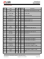
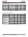
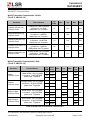
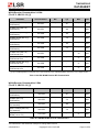
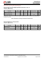
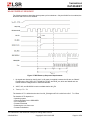
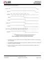
1
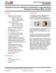
TiWi5 MODULE DATASHEET Integrated Transceiver Modules for WLAN 802.11 a/b/g/n, Bluetooth, Bluetooth Low Energy (BLE), and ANT FEATURES DESCRIPTION IEEE 802.11 a,b,g,n,d,e,I compliant Typical WLAN Transmit Power: o 18.3 dBm, 11 Mbps, CCK (b) o 14.4 dBm, 54 Mbps, OFDM (g) o 12.5 dBm, 65 Mbps, OFDM (n) Typical WLAN Sensitivity: o -88 dBm, 8% PER,11 Mbps o -74 dBm, 10% PER, 54 Mbps o -72 dBm, 10% PER, 65 Mbps Bluetooth 2.1+EDR, Power Class 1.5 Full support for BLE 4.0 and ANT Miniature footprint: 18 mm x 13 mm Low height profile: 1.9 mm Terminal for PCB/Chip antenna feeds Worldwide acceptance: FCC (USA), IC (Canada), and CE (Europe) Modular certification allows reuse of LSR FCC ID and ETSI certification without repeating the expensive testing on your end product Compact design based on Texas Instruments WL1273L Transceiver Seamless integration with TI OMAP™ application processors SDIO Host data path interfaces Bluetooth Advanced Audio Interfaces Low power operation modes RoHS compliant Streamlined development with LSR Design Services APPLICATIONS Security HVAC Control, Smart Energy Sensor Networks Medical The TiWi5 module is a high performance 2.4 /5.5 GHz IEEE 802.11 a/b/g/n, Bluetooth 2.1+EDR, and Bluetooth Low Energy (BLE) 4.0 radio in a cost effective, pre-certified footprint. The module realizes the necessary PHY/MAC layers to support WLAN applications in conjunction with a host processor over a SDIO interface. The module also provides a Bluetooth platform through the UART or btSPI HCI transport layer. Both WLAN and Bluetooth share the same antenna port. TiWi5 is pin for pin compatible with the TiWi-R2 and TiWi-BLE modules. TiWi5 does not include the on module U.FL connector. Need to get to market quickly? Not an expert in 802.11 or Bluetooth? Need a custom antenna? Would you like to own the design? Would you like a custom design? Not quite sure what you need? Do you need help with your host board? LSR Design Services will be happy to develop custom hardware or software, integrate the design, or license the design so you can manufacture yourself. Contact us at [email protected] or call us at 262-375-4400. The information in this document is subject to change without notice. 330-0042-R2.6 Copyright © 2011-2015 LSR Page 1 of 56 TiWi5 MODULE DATASHEET ORDERING INFORMATION Order Number 450-0053 450-0053R Description TiWi5 Module (Tray, SPQ = 100) TiWi5 Module (Tape and Reel, SPQ = 1000) Table 1 Orderable TiWi5 Part Numbers MODULE ACCESSORIES Order Number Description 001-0009 2.4/5.5 GHz Dual-Band Dipole Antenna with Reverse Polarity SMA Connector 080-0001 U.FL to Reverse Polarity SMA Bulkhead Cable 105mm Table 2 Module Accessories The information in this document is subject to change without notice. 330-0042-R2.6 Copyright © 2011-2015 LSR Page 2 of 56 TiWi5 MODULE DATASHEET BLOCK DIAGRAM Figure 1 TiWi5 Module Block Diagram – Top-Level The information in this document is subject to change without notice. 330-0042-R2.6 Copyright © 2011-2015 LSR Page 3 of 56 TiWi5 MODULE DATASHEET TABLE OF CONTENTS FEATURES .......................................................................................................................... 1 APPLICATIONS ................................................................................................................... 1 DESCRIPTION ..................................................................................................................... 1 ORDERING INFORMATION ................................................................................................ 2 MODULE ACCESSORIES ................................................................................................... 2 BLOCK DIAGRAM ............................................................................................................... 3 PIN DESCRIPTIONS ............................................................................................................ 8 BT_FUNC2 and BT_FUNC5 Pins ............................................................................................................. 10 BT_FUNC4 Pin ........................................................................................................................................... 10 WL_UART_DBG Pin .................................................................................................................................. 10 WL_RS232_RX and WL_RS232_TX Pins ................................................................................................ 10 INI FILE RADIO PARAMETERS ........................................................................................ 11 5 GHZ AP MODE ............................................................................................................... 12 ELECTRICAL SPECIFICATIONS ...................................................................................... 13 Absolute Maximum Ratings ..................................................................................................................... 13 Recommended Operating Conditions .................................................................................................... 13 General Characteristics ............................................................................................................................ 14 WLAN RF Characteristics......................................................................................................................... 17 Bluetooth RF Characteristics .................................................................................................................. 19 Bluetooth Low Energy RF Characteristics ............................................................................................. 20 WLAN POWER-UP SEQUENCE ....................................................................................... 21 WLAN POWER-DOWN SEQUENCE ................................................................................. 22 BLUETOOTH POWER-UP SEQUENCE............................................................................ 23 BLUETOOTH POWER-DOWN SEQUENCE ..................................................................... 24 ENABLE SCHEME ............................................................................................................ 25 IRQ OPERATION ............................................................................................................... 25 SLOW (32 KHZ) CLOCK SOURCE REQUIREMENTS ..................................................... 26 The information in this document is subject to change without notice. 330-0042-R2.6 Copyright © 2011-2015 LSR Page 4 of 56 TiWi5 MODULE DATASHEET BLUETOOTH HCI UART ................................................................................................... 27 BLUETOOTH AUDIO CODEC INTERFACE ..................................................................... 29 Overview .................................................................................................................................................... 29 PCM Hardware Interface ........................................................................................................................... 29 Data Format ............................................................................................................................................... 29 Frame-Idle Period ...................................................................................................................................... 30 Clock-Edge Operation .............................................................................................................................. 31 Two Channel PCM Bus Example ............................................................................................................. 31 Audio Encoding ......................................................................................................................................... 32 Improved Algorithm for Lost Packets ..................................................................................................... 32 BLUETOOTH PCM CLOCK MISMATCH HANDLING....................................................... 33 BLUETOOTH INTER-IC SOUND (I2S) .............................................................................. 34 UDI SUPPORT ................................................................................................................... 35 ADVANCED AUDIO FEATURES ...................................................................................... 36 Wideband (WB) Speech ............................................................................................................................ 36 Assisted A2DP ........................................................................................................................................... 37 SDIO INTERFACE TIMING ................................................................................................ 38 SDIO CLOCK TIMING........................................................................................................ 39 SOLDERING RECOMMENDATIONS ................................................................................ 40 Recommended Reflow Profile for Lead Free Solder ............................................................................. 40 CLEANING ......................................................................................................................... 41 OPTICAL INSPECTION ..................................................................................................... 41 REWORK ........................................................................................................................... 41 SHIPPING, HANDLING, AND STORAGE ......................................................................... 41 Shipping ..................................................................................................................................................... 41 Handling ..................................................................................................................................................... 41 Moisture Sensitivity Level (MSL) ............................................................................................................. 41 Storage ....................................................................................................................................................... 41 Repeating Reflow Soldering .................................................................................................................... 42 AGENCY CERTIFICATIONS ............................................................................................. 43 The information in this document is subject to change without notice. 330-0042-R2.6 Copyright © 2011-2015 LSR Page 5 of 56 TiWi5 MODULE DATASHEET AGENCY STATEMENTS ................................................................................................... 43 Federal Communication Commission Interference Statement ............................................................ 43 Industry Canada Statements.................................................................................................................... 45 OEM RESPONSIBILITIES TO COMPLY WITH FCC AND INDUSTRY CANADA REGULATIONS ....................................................................................................... 47 OEM LABELING REQUIREMENTS FOR END-PRODUCT .............................................. 48 OEM END PRODUCT USER MANUAL STATEMENTS.................................................... 49 EUROPE ............................................................................................................................ 50 CE Notice ................................................................................................................................................... 50 Declaration of Conformity (DOC) ............................................................................................................ 50 MECHANICAL DATA......................................................................................................... 51 PCB FOOTPRINT .............................................................................................................. 52 TAPE AND REEL SPECIFICATION .................................................................................. 53 DEVICE MARKINGS .......................................................................................................... 54 Rev 1 Devices ............................................................................................................................................ 54 Rev 2 Devices ............................................................................................................................................ 54 Rev 3 Devices ............................................................................................................................................ 55 CONTACTING LSR............................................................................................................ 56 The information in this document is subject to change without notice. 330-0042-R2.6 Copyright © 2011-2015 LSR Page 6 of 56 TiWi5 MODULE DATASHEET TIWI5 MODULE FOOTPRINT AND PIN DEFINITIONS To apply the TiWi5 module, it is important to use the module pins in your application as they are designated in below and in the corresponding pin definition table found on pages 8 and 9. Not all the pins on the TiWi5 module may be used, as some are reserved for future functionality. Figure 2 TiWi5 Pinout (Top View) The information in this document is subject to change without notice. 330-0042-R2.6 Copyright © 2011-2015 LSR Page 7 of 56 TiWi5 MODULE DATASHEET PIN DESCRIPTIONS Module Pin Name I/O Type Buffer Type Logic Level 1 VBAT PI - - 2 BT_FUNC5 DO 4 mA 1.8 VDC HOST_WU (*) 3 WL_UART_DBG DIO 4 mA 1.8 VDC WL_UART_DBG 4 WLAN_IRQ DO 4 mA 1.8 VDC WLAN Interrupt Request 5 BT_EN DI - 1.8 VDC Bluetooth Enable 6 FM_EN DI - 1.8 VDC NOT SUPPORTED, CONNECT TO GND 7 WL_RS232_RX DI - 1.8 VDC WLAN TEST UART RX (*) 8 WL_RS232_TX DO 4 mA 1.8 VDC WLAN TEST UART TX (*) 9 FM_I2S_FSYNC DO 4 mA 1.8 VDC NOT SUPPORTED, NO CONNECT 10 WL_EN DI - 11 VIO PI - - POWER SUPPLY FOR 1.8 VDC DIGITAL DOMAIN 12 GND GND - - Ground 13 SDIO_D3 DIO 8 mA 1.8 VDC SDIO INTERFACE, HOST PULL UP 14 SDIO_D2 DIO 8 mA 1.8 VDC SDIO INTERFACE, HOST PULL UP 15 SDIO_D1 DIO 8 mA 1.8 VDC SDIO INTERFACE, HOST PULL UP 16 SDIO_D0 DIO 8 mA 1.8 VDC SDIO INTERFACE, HOST PULL UP 17 SDIO_CMD DIO 8 mA 1.8 VDC HOST PULL UP 18 SDIO_CLK DI - 1.8 VDC HOST PULL UP 19 SLOW_CLK DI - 1.8 VDC SLEEP CLOCK (32 kHz) 20 FM_IRQ DO 4 mA 1.8 VDC NOT SUPPORTED, NO CONNECT 21 FM_SDA DO 4 mA 1.8 VDC NOT SUPPORTED, NO CONNECT 22 FM_SCL DO 4 mA 1.8 VDC NOT SUPPORTED, NO CONNECT 23 FM_I2S_CLK DO 4 mA 1.8 VDC NOT SUPPORTED, NO CONNECT 24 FM_I2S_DI DI 4 mA 1.8 VDC NOT SUPPORTED, CONNECT TO GND 25 FM_I2S_DO DO 4 mA 1.8 VDC NOT SUPPORTED, NO CONNECT 26 FM_AUD_RIN AI - - NOT SUPPORTED, CONNECT TO GND 27 FM_AUD_LIN AI - - NOT SUPPORTED, CONNECT TO GND 28 FMRFOUT AO - - NOT SUPPORTED, NO CONNECT 29 FMRFIN AI - - NOT SUPPORTED, CONNECT TO GND 30 GND GND - - Ground 31 FM_AUD_ROUT AO - - NOT SUPPORTED, NO CONNECT Description Battery Voltage 3.6 VDC Nominal (3.0-4.8 VDC) 1.8 VDC WLAN Enable The information in this document is subject to change without notice. 330-0042-R2.6 Copyright © 2011-2015 LSR Page 8 of 56 TiWi5 MODULE DATASHEET Module Pin Name I/O Type Buffer Type Logic Level 32 FM_AUD_LOUT AO - - 33 AUD_FSYNC DIO 4 mA 1.8 VDC PCM I/F 34 HCI_RX DI 8 mA 1.8 VDC Bluetooth HCI UART RX (*) 35 HCI_RTS DO 4 mA 1.8 VDC Bluetooth HCI UART RTS (*) 36 HCI_TX DIO 8 mA 1.8 VDC Bluetooth HCI UART TX 37 AUD_CLK DO 4 mA 1.8 VDC PCM I/F (*) 38 AUD_OUT DO 4 mA 1.8 VDC PCM I/F (*) 39 HCI_CTS DI 4 mA 1.8 VDC Bluetooth HCI UART CTS (*) 40 AUD_IN DI 4 mA 1.8 VDC PCM I/F (*) 41 BT_FUNC2 DI 4 mA 1.8 VDC Bluetooth Wakeup[DI] / DC2DC mode[DO](*) 42 BT_FUNC4 DO 4 mA 1.8 VDC BT_UARTD (DEBUG) (*) 43 VDD_LDO_CLASS_1P5 NC - - VBAT VOLTAGE PRESENT, NO CONNECT 44 GND GND - - Ground 45 GND GND - - Ground 46 GND GND - - Ground 47 GND GND - - Ground 48 ANT RF - Antenna terminal for WLAN and Bluetooth (note [1]) 49 GND GND - - Ground 50 GND GND - - Ground 51 GND GND - - Ground 52 GND GND - - Ground PI = Power Input AI = Analog Input PO = Power Output AO = Analog Output Description NOT SUPPORTED, NO CONNECT DI = Digital Input (1.8 VDC Logic Level) DO = Digital Output (1.8 VDC Logic Level) AIO = Analog Input/Output RF = RF Port GND = Ground Note[1]: Antenna terminal presents DC short circuit to ground. (*) indicates that pin is capable of bidirectional operation, but is used as the type shown. Table 3 TiWi5 Module Pin Descriptions All digital I/O signals use 1.8V logic. If the host microcontroller does not support 1.8V logic, then level shifters MUST be used. The information in this document is subject to change without notice. 330-0042-R2.6 Copyright © 2011-2015 LSR Page 9 of 56 TiWi5 MODULE DATASHEET BT_FUNC2 and BT_FUNC5 Pins When BT is awake and active, BT_WU (BT_FUNC2) is high (from host to module). This is an active high signal. The host puts the BT section to sleep by de-asserting (logic low level) the BT_WU signal (input to the module). The module then drives HOST_WU (BT_FUNC5) low to acknowledge to the host that it is has been put into sleep mode. Using these pins is optional. BT_FUNC4 Pin The BT_FUNC4 (BT_UARTD) pin is a debug pin. It is a 1.8V logic UART TX line. This pin should never need to be used in normal operation. It may be useful to terminate this pin to a test point or header in case it is needed. WL_UART_DBG Pin The WL_UART_DBG pin is a debug pin. It is a 1.8V logic UART TX line. This pin should never need to be used in normal operation. It may be useful to terminate this pin to a test point or header in case it is needed. WL_RS232_RX and WL_RS232_TX Pins This pins are used for a WLAN test mode interface. Both pins are 1.8V logic level UART pins. These pins should be brought out to a header on the host PCB. The WLAN test interface can be used to place the module into constant packet transmit and constant packet receive modes. These modes can be useful for antenna and sensitivity testing. The information in this document is subject to change without notice. 330-0042-R2.6 Copyright © 2011-2015 LSR Page 10 of 56 TiWi5 MODULE DATASHEET INI FILE RADIO PARAMETERS There is an ini file that contains WLAN radio parameters which are critical to both the RF performance and EMC compliance of the module. The ini file available on the LSR wiki is only intended to be used with the LSR WLAN Eval Tool. Note that this ini file will not work when using the TiWi5 module in normal operation which typically involves an operating system. To use the TiWi5 module in normal operation, refer to specifics contained in the TiWi Family INI File Radio Parameter User Guide which is also available for download on the LSR website. The settings specified in the appropriate ini file must be used to operate the module in compliance with the modular certification for FCC or ETSI. There is a unique ini file for operating the module in compliance with FCC regulations, and a different ini file for operating the module in compliance with the ETSI regulations. The information in this document is subject to change without notice. 330-0042-R2.6 Copyright © 2011-2015 LSR Page 11 of 56 TiWi5 MODULE DATASHEET 5 GHZ AP MODE The TiWi5 module was not certified as a DFS Master, and therefore the AP mode is not allowed in the 5 GHz bands. The AP mode is allowed to be used in the 2.4 GHz band. Software cannot prevent the usage of the AP mode in the 5 GHz band, so it is the module-integrators responsibility to ensure the 5 GHz AP mode is not used. The information in this document is subject to change without notice. 330-0042-R2.6 Copyright © 2011-2015 LSR Page 12 of 56 TiWi5 MODULE DATASHEET ELECTRICAL SPECIFICATIONS The majority of these characteristics are based on controlling and conditioning the tests using the TiWi5 control software application. Other control conditions may require these values to be re-characterized by the customer. Absolute Maximum Ratings Parameter Min Max Unit Power supply voltage (VBAT)(4)(5) -0.5 +5.5 V Digital supply voltage (VIO) -0.5 2.1 V Voltage on any GPIO -0.5 VIO + 0.5 V Voltage on any Analog Pins(3) -0.5 2.1 V +10 dBm -40 +85 ºC -55 +125 ºC RF input power, antenna port Operating temperature(6) Storage temperature 1. 2. 3. 4. 5. 6. Stresses beyond those listed under “absolute maximum ratings” may cause permanent damage to the device and are not covered by the warranty. These are stress ratings only and functional operation of the device at these or any other conditions beyond those indicated under “recommended operating conditions” is not implied. Exposure to absolutemaximum-rated conditions for extended periods may affect device reliability. All parameters are measured as follows unless stated otherwise: VDD_IN=1.8V, VDDIO_1.8V=1.8V, VDD_LDO_CLASS1P5=3.6V Analog pins: XTALP, XTALM, RFIOBT, DRPWRXBM, DRPWRXBP, DRPWTXB, and also FMRFINP, FMRFINM, FMRFINM, FMAUDLIN, FMAUDRIN, FMAUDLOUT, FMAUDROUT The following signals are from the VBAT group, PMS_VBAT and VDD_LDO_CLASS1P5 (if BT class 1.5 direct VBAT is used). Maximum allowed depends on accumulated time at that voltage; 4.8V for 7 years lifetime, 5.5V for 6 hours cumulative. The device can be reliably operated for 5,000 active-WLAN cumulative hours at TA of 85oC. Table 4 Absolute Maximum Ratings Recommended Operating Conditions Parameter Min Typ Max Unit VBAT 3.0 3.6 4.8 V VIO 1.62 1.8 1.92 V VIH 0.65 x VIO - VIO V VIL 0 - 0.35 x VIO V VOH @ 4, 8 mA VIO - 0.45 - VIO V VOL @ 4, 8 mA 0 - 0.45 V -40 25 85 ºC Ambient temperature range Table 5 Recommended Operating Conditions The information in this document is subject to change without notice. 330-0042-R2.6 Copyright © 2011-2015 LSR Page 13 of 56 TiWi5 MODULE DATASHEET General Characteristics Parameter Min WLAN RF frequency range 1 WLAN RF frequency range 2 WLAN RF data rate Max Unit 2412 2472 MHz 4910 5835 MHz 65 Mbps 2480 MHz 1 BT RF frequency Range Typ 802.11 a/b/g/n rates supported 2402 Table 6 General Characteristics Power Consumption – WLAN 2.4 GHz Parameter Test Conditions Min Typ Max Unit CCK (802.11b) TX Current 2437 MHz, VBAT =3.6V, Tamb=+25°C Po=18.3 dBm, 11 Mbps CCK L=1200 bytes, tdelay (idle)=4 S - 247 - mA OFDM (802.11g) TX Current 2437 MHz, VBAT =3.6V, Tamb=+25°C Po=14.4 dBm, 54 Mbps OFDM L=1200 bytes, tdelay (idle)=4 S - 180 - mA OFDM (802.11n) TX Current 2437 MHz, VBAT =3.6V, Tamb=+25°C Po=12.5 dBm, 65 Mbps OFDM L=1200 bytes, tdelay (idle)=4 S - 166 - mA CCK (802.11b) RX Current - 93 - mA OFDM (802.11g) RX Current - 93 - mA OFDM (802.11n) RX Current - 93 - mA Dynamic Mode [1] - <1.2 - mA [1] Total Current from VBAT for reception of Beacons with DTIM=1 TBTT=100 mS, Beacon duration 1.6ms, 1 Mbps beacon reception in Listen Mode. Table 7 2.4 GHz WLAN Power Consumption The information in this document is subject to change without notice. 330-0042-R2.6 Copyright © 2011-2015 LSR Page 14 of 56 TiWi5 MODULE DATASHEET Power Consumption – WLAN 5 GHz Parameter Test Conditions Min Typ Max Unit OFDM 9 Mbps (802.11a) TX Current 5745 MHz, VBAT =3.6V, Tamb=+25°C Po=17.6 dBm, 9 Mbps OFDM L=1200 bytes, tdelay (idle)=4 S - 296 - mA OFDM 54 Mbps (802.11a) TX Current 5745 MHz, VBAT =3.6V, Tamb=+25°C Po=15.0 dBm, 54 Mbps OFDM L=1200 bytes, tdelay (idle)=4 S - 235 - mA MCS0 6.5 Mbps (802.11a) TX Current 5745 MHz, VBAT =3.6V, Tamb=+25°C Po=18.0 dBm, MCS0 OFDM L=1200 bytes, tdelay (idle)=4 S - 298 - mA MCS7 65 Mbps (802.11a) TX Current 5745 MHz, VBAT =3.6V, Tamb=+25°C Po=13.2 dBm, MCS7 OFDM L=1200 bytes, tdelay (idle)=4 S - 219 - mA 54/65 Mbps (802.11a/n) RX Current - 100 - mA Dynamic Mode [1] - <1.2 - mA [1] Total Current from VBAT for reception of Beacons with DTIM=1 TBTT=100 mS, Beacon duration 1.6ms, 1 Mbps beacon reception in Listen Mode. Table 8 5 GHz WLAN Power Consumption The information in this document is subject to change without notice. 330-0042-R2.6 Copyright © 2011-2015 LSR Page 15 of 56 TiWi5 MODULE DATASHEET Power Consumption - Bluetooth Parameter Test Conditions Min Typ Max Unit GFSK TX Current Constant Transmit, 1DH5, PRBS9 - 45 - mA EDR TX Current Constant Transmit, 2DH5,3DH5, PRBS9 - 43 - mA GFSK RX Current Constant Receive, 1DH1 - 35 - mA EDR RX Current Constant Receive, 2DH5, 3DH5 - 41 - mA Deep Sleep Current Deep Sleep Mode - 70 - µA Typ Max Unit - 16 mA Table 9 Bluetooth Power Consumption DC Characteristics – General Purpose I/O Parameter Test Conditions Min VIO Current Logic input low, VIL 0 - 0.35 x VIO V Logic input high, VIH 0.65 x VIO - VIO V Logic output low, VOL (Full Drive) Iout = 8 mA 0 - 0.45 V Iout = 4 mA 0 - 0.45 V Logic output low, VOL (Reduced Drive) Iout = 1 mA 0 - 0.112 V Iout = 0.09 mA 0 - 0.01 V Logic output high, VOH (Full Drive) Iout = -8 mA VIO - 0.45 - VIO V Iout = -4 mA VIO - 0.45 - VIO V Logic output high, VOH (Reduced Drive) Iout = -1 mA VIO - 0.112 - VIO V Iout = -0.3 mA VIO - 0.033 - VIO V Table 10 DC Characteristics General Purpose I/O The information in this document is subject to change without notice. 330-0042-R2.6 Copyright © 2011-2015 LSR Page 16 of 56 TiWi5 MODULE DATASHEET WLAN RF Characteristics WLAN Transmitter Characteristics 2.4 GHz (TA=25°C, VBAT=3.6 V) Test Conditions Typ EVM Min Typ Max Unit 11 Mbps CCK (802.11b) TX Output Power 11 Mbps CCK , 802.11(b) Mask Compliance, 35% EVM RMS power over TX packet 1.1 - 18.3 - dBm 9 Mbps OFDM (802.11g) TX Output Power 9 Mbps OFDM , 802.11(g) Mask Compliance, -8 dB EVM RMS power over TX packet -24 - 18.0 - dBm 54 Mbps OFDM (802.11g) TX Output Power 54 Mbps OFDM, 802.11(g) Mask Compliance, -25 dB EVM RMS power over TX packet -34 - 14.4 - dBm -24 - 18.2 - dBm -35 - 12.5 - dBm Parameter 6.5 Mbps OFDM (802.11n) TX Output Power 65 Mbps OFDM (802.11n) TX Output Power 6.5 Mbps OFDM, 802.11(n) Mask Compliance, -5 dB EVM RMS power over TX packet 65 Mbps OFDM, 802.11(n) Mask Compliance, -28 dB EVM RMS power over TX packet Table 11 WLAN 2.4 GHz Transmitter RF Characteristics WLAN Transmitter Characteristics 5 GHz (TA=25°C, VBAT=3.6 V) Parameter 9 Mbps TX Output Power 54 Mbps TX Output Power MCS0 6.5 Mbps TX Output Power MCS7 65 Mbps TX Output Power Test Conditions 9 Mbps OFDM , 802.11(a) Mask Compliance, -8 dB EVM RMS power over TX packet 54 Mbps OFDM , 802.11(a) Mask Compliance, -25 dB EVM RMS power over TX packet MCS0 OFDM , 802.11(a) Mask Compliance, -5 dB EVM RMS power over TX packet MCS7 OFDM , 802.11(a) Mask Compliance, -27 dB EVM RMS power over TX packet Typ EVM Start Freq -31 5170 -28 5260 -21 5745 17.8 5825 -31 5170 13.0 5240 -30 5260 -28 5745 15.2 5825 -31 5170 13.1 5240 -28 5260 -21 5745 18.2 5825 -31 5170 12.5 5240 -31 5260 -29 5745 Min Typ Max 13.0 - - - - 15.6 14.6 15.7 12.8 13.5 End Freq Unit 5240 - - - - 5700 5700 5700 5700 dBm dBm dBm dBm 5825 Table 12 WLAN 5 GHz Transmitter RF Characteristics The information in this document is subject to change without notice. 330-0042-R2.6 Copyright © 2011-2015 LSR Page 17 of 56 TiWi5 MODULE DATASHEET WLAN Receiver Characteristics 2.4 GHz (TA=25°C, VBAT=3.6 V) [1] Parameter Test Conditions Min Typ Max Unit 1 Mbps CCK (802.11b) RX Sensitivity 8% PER - -97 - dBm 11 Mbps CCK (802.11b) RX Sensitivity 8% PER - -88 - dBm 9 Mbps OFDM (802.11g) RX Sensitivity 10% PER - -89 - dBm 54 Mbps OFDM (802.11g) RX Sensitivity 10% PER - -74 - dBm 6.5 Mbps OFDM (802.11n) RX Sensitivity 10% PER - -89 - dBm 65 Mbps OFDM (802.11n) RX Sensitivity 10% PER - -72 - dBm 11 Mbps CCK (802.11b) RX Overload Level 8% PER - - -10 dBm 9 Mbps OFDM (802.11g) RX Overload Level 10% PER - - -17 dBm 54 Mbps OFDM (802.11g) RX Overload Level 10% PER - - -17 dBm 65 Mbps OFDM (802.11n) RX Overload Level 10% PER - - -17 dBm [1] Up to 2 dB degradation at Channel 13 for 11g/n modes and up to 2 dB degradation at Channel 14 for 11b/g/n modes. Table 13 2.4 GHz WLAN Receiver RF Characteristics WLAN Receiver Characteristics 5 GHz (TA=25°C, VBAT=3.6 V) [1] Parameter Test Conditions Min Typ Max Unit 9 Mbps (802.11a) RX Sensitivity 10% PER - -87 - dBm 54 Mbps (802.11a) RX Sensitivity 10% PER - -72 - dBm MCS0 6.5 Mbps (802.11a) RX Sensitivity 10% PER - -88 - dBm MCS7 65 Mbps (802.11a) RX Sensitivity 10% PER - -70 - dBm <10% PER - - -17 dBm Max Input Level (3) OFDM (11a or 11n) Table 14 5 GHz WLAN Receiver RF Characteristics The information in this document is subject to change without notice. 330-0042-R2.6 Copyright © 2011-2015 LSR Page 18 of 56 TiWi5 MODULE DATASHEET Bluetooth RF Characteristics Bluetooth Transmitter GFSK and EDR Characteristics, Class 1.5 (TA=25°C, VBAT=3.6 V) Parameter Test Conditions Min Typ Max Bluetooth Spec Unit GFSK RF Output Power - 9.5 - - dBm EDR RF Output Power - 7.3 - Power Control Step Size 2 5 8 2-8 dB EDR Relative Power -2 1 -4/+1 dB dBm Table 15 Bluetooth Transmitter RF Characteristics Bluetooth Receiver Characteristics (TA=25°C, VBAT=3.6 V) Test Conditions Min Typ Max Bluetooth Spec Unit GFSK Sensitivity BER=0.1% - -91 - -70 dBm EDR 2 Mbps Sensitivity BER=0.01% - -90 - -70 dBm EDR 3 Mbps Sensitivity BER=0.01% - -83 - -70 dBm GFSK Maximum Input Level BER=0.1% - - -5 -20 dBm EDR 2 Maximum Input Level BER=0.1% - - -10 - dBm EDR 3 Maximum Input Level BER=0.1% - - -10 - dBm Parameter Table 16 Bluetooth Receiver RF Characteristics The information in this document is subject to change without notice. 330-0042-R2.6 Copyright © 2011-2015 LSR Page 19 of 56 TiWi5 MODULE DATASHEET Bluetooth Low Energy RF Characteristics Bluetooth BLE Transmitter GMSK and EDR Characteristics, Class 1.5 (TA=25°C, VBAT=3.6 V) Test Conditions Parameter Min Typ Max Bluetooth Spec Unit GMSK RF Output Power - 10 - - dBm Power Control Step Size 2 5 8 2-8 dB (1) BLE spec = 10dBm max can be achieved using normal system losses due to filters etc, or by reducing value through VS command. Table 17 Bluetooth Low Energy Transmitter RF Characteristics Bluetooth BLE Receiver Characteristics (TA=25°C, VBAT=3.6 V) Test Conditions Min Typ Max Bluetooth Spec Unit GMSK Sensitivity PER = 30.8% - -90 - -70 dBm GMSK Maximum Input Level PER = 30.8% - -5 - -20 dBm Parameter Table 18 Bluetooth Low Energy Receiver RF Characteristics The information in this document is subject to change without notice. 330-0042-R2.6 Copyright © 2011-2015 LSR Page 20 of 56 TiWi5 MODULE DATASHEET WLAN POWER-UP SEQUENCE The following sequence describes device power-up from shutdown. Only the WLAN Core is enabled; the Bluetooth and FM cores are disabled. Figure 3 TiWi5 Power-up Sequence Requirements 1. No signals are allowed on the IO pins if no IO power is supplied, because the IOs are not 'failsafe’. Exceptions are CLK_REQ_OUT, SLOWCLK, XTALP, and AUD_xxx, which are failsafe and can tolerate external voltages with no VDDS and DC2DC. 2. VBAT, VIO, and SLOWCLK must be available before WL_EN. 3. Twakeup = T1 + T2 The duration of T1 is defined as the time from WL_EN=high until Fref is valid for the SoC. T1=~55ms The duration of T2 depends on: – Operating system – Host enumeration for the SDIO/WSPI – PLL configuration – Firmware download – Releasing the core from reset – Firmware initialization The information in this document is subject to change without notice. 330-0042-R2.6 Copyright © 2011-2015 LSR Page 21 of 56 TiWi5 MODULE DATASHEET WLAN POWER-DOWN SEQUENCE Notes: 1. The DC2DC(1.8V) signal can be monitored on BT_FUNC2 Module Pin (#41) 2. DC_REQ and CLK_REQ are internal signals shown for reference only Figure 4 TiWi5 Module Power-down Sequence Requirements 1. DC_REQ will go low only if WLAN is the only core working. Otherwise if another core is working (e.g BT) it will stay high. 2. CLK_REQ will go low only if WLAN is the only core working. Otherwise if another core is working and using the FREF (e.g BT) it will stay high. 3. If WLAN is the only core that is operating, WL_EN must remain de-asserted for at least 64sec before it is re-asserted. The information in this document is subject to change without notice. 330-0042-R2.6 Copyright © 2011-2015 LSR Page 22 of 56 TiWi5 MODULE DATASHEET BLUETOOTH POWER-UP SEQUENCE The following sequence describes device power up from shutdown. Only the Bluetooth core is enabled; the WLAN core is disabled. Notes: 1. (A) After this sequence is completed, the device is in the low VIO-leakage state while in shutdown 2. The DC2DC(1.8V) signal can be monitored on BT_FUNC2 Module Pin (#41) 3. DC_REQ, CLK_REQ, and FREF are internal signals shown for reference only Figure 5 Bluetooth Power-up Sequence Power up requirements: 1. No signals are allowed on the IO pins if no IO power supplied, because the IOs are not 'failsafe'. Exceptions are CLK_REQ_OUT, SLOWCLK, XTALP, and AUD_xxx, which are failsafe and can tolerate external voltages with no VDDS and DC2DC. 2. VDDS and SLOWCLK must be stable before releasing BT_EN. 3. Fast clock must be stable maximum 55 ms after BT_EN goes HIGH. The information in this document is subject to change without notice. 330-0042-R2.6 Copyright © 2011-2015 LSR Page 23 of 56 TiWi5 MODULE DATASHEET BLUETOOTH POWER-DOWN SEQUENCE Notes: 1. The DC2DC(1.8V) signal can be monitored on BT_FUNC2 Module Pin (#41) 2. DC_REQ and CLK_REQ are internal signals shown for reference only Figure 6 Bluetooth Power-down Sequence The TiWi5 module indicates completion of Bluetooth power-up sequence by asserting HCI_RTS low. This occurs up to 100 ms after BT_EN goes high. The information in this document is subject to change without notice. 330-0042-R2.6 Copyright © 2011-2015 LSR Page 24 of 56 TiWi5 MODULE DATASHEET ENABLE SCHEME The module has 3 enable pins, one for each core: WL_EN, and BT_EN and FM_EN. Presently, there are 2 modes of active operation now supported: WLAN and Bluetooth. It is recommended that the FM_EN pin be grounded to disable the FM section. It is also recommended that the FM section be disabled by Bluetooth HCI commands. 1. Each core is operated independently by asserting each EN signal to Logic '1'. In this mode it is possible to control each core asynchronously and independently. 2. Bluetooth mode operation. WLAN will be operated through WL_EN asynchronously and independently of Bluetooth. IRQ OPERATION 1. The default state of the WLAN_IRQ prior to firmware initialization is 0. 2. During firmware initialization, the WLAN_IRQ is configured by the SDIO module; a WLAN_IRQ changes its state to 1. 3. A WLAN firmware interrupt is handled as follows: a. The WLAN firmware creates an Interrupt-to-Host, indicated by a 1-to-0 transition on the WLAN_IRQ line (host must be configured as active-low or falling-edge detect). b. After the host is available, depending on the interrupt priority and other host tasks, it masks the firmware interrupt. The WLAN_IRQ line returns to 1 (0-to-1 transition on the WLAN_IRQ line). c. The host reads the internal register status to determine the interrupt sources - the register is cleared after the read. d. The host processes in sequence all the interrupts read from this register e. The host unmasks the firmware interrupts. 4. The host is ready to receive another interrupt from the WLAN device. The information in this document is subject to change without notice. 330-0042-R2.6 Copyright © 2011-2015 LSR Page 25 of 56 TiWi5 MODULE DATASHEET SLOW (32 KHZ) CLOCK SOURCE REQUIREMENTS The slow clock is always supplied from an external source. It is input on the SLOW_CLK pin, and can be a digital signal in the range of VIO only. For slow clock frequency and accuracy refer to Table 19. The external slow clock must be stable before the system exits from shut down mode. Parameter [1] Condition Symbol Min Input slow clock frequency WLAN, BT Input transition time Tr/Tf – 10% to 90% Tr/Tf Frequency input duty cycle VIL Max 32768 Input slow clock accuracy Input voltage limits Typ 30 Square wave, DC coupled VIH 0 50 0.65 x VDDS Unit Hz +/-250 ppm 100 ns 70 % VDDS Vpeak 0.35 x VDDS Input impedance 1 MW Input capacitance 5 pF Rise and fall time 100 ns Phase noise 1 kHz -125 dBc/Hz [1] Slow clock is a fail safe input Table 19 Slow Clock Source Requirements The information in this document is subject to change without notice. 330-0042-R2.6 Copyright © 2011-2015 LSR Page 26 of 56 TiWi5 MODULE DATASHEET BLUETOOTH HCI UART Figure 7 Bluetooth UART Timing Table 20 Bluetooth UART Timing The information in this document is subject to change without notice. 330-0042-R2.6 Copyright © 2011-2015 LSR Page 27 of 56 TiWi5 MODULE DATASHEET Figure 8 Bluetooth UART Data Frame Table 21 Bluetooth UART Data Frame The information in this document is subject to change without notice. 330-0042-R2.6 Copyright © 2011-2015 LSR Page 28 of 56 TiWi5 MODULE DATASHEET BLUETOOTH AUDIO CODEC INTERFACE Overview The CODEC interface is a fully dedicated programmable serial port that provides the logic to interface to several kinds of PCM or I2S codecs. The interface supports: Two voice channels Master / slave modes Coding schemes: μ-Law, A-Law, Linear, Transparent Long & short frames Different data sizes, order and positions UDI profile High rate PCM interface for EDR Enlarged interface options to support a wider variety of Codecs PCM bus sharing PCM Hardware Interface The PCM interface is one implementation of the codec interface. It contains the following four lines: Clock--configurable direction (input or output) Frame Sync--configurable direction (input or output) Data In--Input Data Out--Output/Hi-Z The WL1273L device can be either the master of the interface where it generates the clock and the framesync signals, or slave where it receives these two signals. The PCM interface is fully configured by means of a VS command. For slave mode, clock input frequencies of up to 16MHz are supported. At clock rates above 12MHz, the maximum data burst size is 32 bits. For master mode, the WL1273L can generate any clock frequency between 64kHz and 4.096MHz. Data Format The data format is fully configurable: The data length can be from 8 to 320 bits, in 1-bit increments, when working with two channels, or up to 640 bits when using 1 channel. The data length can be set independently for each channel. The data position within a frame is also configurable with 1-clock (bit) resolution, and can be set independently (relative to the edge of the Frame Sync signal) for each channel. The Data_In and Data_Out bit order can be configured independently. For example; Data_In can start with MSB while Data_Out starts with LSB. Each channel is separately configurable. The inverse bit order (i.e. LSB first) is supported only for sample sizes up to 24 bits. The data in and data out size do not necessarily have to be the same length. The Data_Out line is configured as a ‘high-Z’ output between data words. Data_Out can also be set for permanent high-Z, irrespective of data out. This allows the WL1273L to be a bus slave in a multi-slave PCM environment. At power up, Data_Out is configured as high-Z. The information in this document is subject to change without notice. 330-0042-R2.6 Copyright © 2011-2015 LSR Page 29 of 56 TiWi5 MODULE DATASHEET Frame-Idle Period The CODEC interface has the capability for frame-idle periods, where the PCM clock can “take a break” and become ‘0’ at the end of the PCM frame, after all data has been transferred. The WL1273L supports frame-idle periods both as master and slave of the PCM bus. When WL1273L is the master of the interface, the frame-idle period is configurable. There are 2 configurable parameters: Clk_Idle_Start - Indicates the number of PCM clock cycles from the beginning of the frame till the beginning of the idle period. After Clk_Idle_Start clock cycles, the clock becomes ‘0’. Clk_Idle_End – Indicates the time from the beginning of the frame till the end of the idle period. This time is given in multiples of PCM clock periods. The delta between Clk_Idle_Start and Clk_Idle_End is the clock idle period. e.g. For PCM clock rate = 1MHz, frame sync period = 10kHz, Clk_Idle_Start = 60, Clk_Idle_End = 90. Between each two-frame sync there are 70 clock cycles (instead of 100). The clock idle period starts 60 clock cycles after the beginning of the frame and lasts 90-60=30 clock cycles. This means that the idle period ends 100-90=10 clock cycles before the end of the frame. The data transmission must end prior to the beginning of the idle period. Figure 9 Frame Idle Period The information in this document is subject to change without notice. 330-0042-R2.6 Copyright © 2011-2015 LSR Page 30 of 56 TiWi5 MODULE DATASHEET Clock-Edge Operation The CODEC interface of the WL1273L can work on the rising or the falling edge of the clock. It also has the ability to sample the frame sync and the data at inversed polarity. The following diagram shows the operation of a falling-edge-clock type of codec. The codec is the master of the PCM bus. The frame-sync signal is updated (by the codec) on the falling clock edge and therefore is sampled (by the WL1273L) on the next rising clock. The data from the codec is sampled (by the WL1273L) on the clock falling edge. Figure 10 Negative Clock Edge PCM Operation Two Channel PCM Bus Example In the following figure, a 2-channel PCM bus is shown where the two channels have different word sizes and arbitrary positions in the bus’ frame. (FT stands for Frame Timer) Figure 11 2 Channels PCM Bus Timing The information in this document is subject to change without notice. 330-0042-R2.6 Copyright © 2011-2015 LSR Page 31 of 56 TiWi5 MODULE DATASHEET Audio Encoding The WL1273L CODEC interface can use one of four audio coding patterns: A-Law (8-bit) μ-Law (8-bit) Linear (8 or 16-bit) Transparent Improved Algorithm for Lost Packets The WL1273L features an improved algorithm for improving voice quality when received voice data packets go missing. There are two options: Repeat the last sample – possible only for sample sizes up to 24 bits. For sample sizes >24 bits, the last byte is repeated. Repeat a configurable sample of 8-24 bits (depends on the real sample size), in order to simulate silence (or anything else) in the PCM bus. The configured sample is written in a specific register for each channel. The choice between those two options is configurable separately for each channel. The information in this document is subject to change without notice. 330-0042-R2.6 Copyright © 2011-2015 LSR Page 32 of 56 TiWi5 MODULE DATASHEET BLUETOOTH PCM CLOCK MISMATCH HANDLING In BT RX, the WL1273L receives RF voice packets and writes these to the CODEC I/F. If the WL1273L receives data faster than the CODEC I/F output allows, an overflow occurs. In this case, the WL1273L BT function has 2 possible behavior modes: ‘allow overflow’ and ‘don’t allow overflow’. If overflow is allowed, the WL1273L BT function continues receiving data and overwrites any data not yet sent to the CODEC. If overflow is not allowed, RF voice packets received when buffer is full, are discarded The information in this document is subject to change without notice. 330-0042-R2.6 Copyright © 2011-2015 LSR Page 33 of 56 TiWi5 MODULE DATASHEET BLUETOOTH INTER-IC SOUND (I2S) The WL1273L can be configured as an Inter-IC Sound (I2S) serial interface to an I2S CODEC device. In this mode, the WL1273L audio CODEC interface is configured as a bi-directional, full duplex interface, with two time slots per frame: Time slot 0 is used for the left channel audio data and time slot 1 for the right channel audio data. Each time slot is configurable up to 40 serial clock cycles in length and the frame is configurable up to 80 serial clock cycles in length. The information in this document is subject to change without notice. 330-0042-R2.6 Copyright © 2011-2015 LSR Page 34 of 56 TiWi5 MODULE DATASHEET UDI SUPPORT The UDI profile defines the protocols and procedures that are used by devices implementing UDI for the 3G mobile phone systems, such as devices with Bluetooth connections to a 3G Handset, communicating via video phone over a 3G network. Up to 2 channels of UDI data can be supported. The data is transferred via the CODEC interface using transparent mode, and is sent out using eSCO EV4 Bluetooth packets (EV5 is also selectable). The information in this document is subject to change without notice. 330-0042-R2.6 Copyright © 2011-2015 LSR Page 35 of 56 TiWi5 MODULE DATASHEET ADVANCED AUDIO FEATURES The WL1273L supports an embedded SBC encoder/decoder (codec) and sample rate converter to achieve enhanced audio/voice options. BLE and ANT are not supported when advanced audio features are active. Wideband (WB) Speech Normal (e)SCO voice links are 8ksamples/s. Proposed enhancements to Bluetooth profiles HFP, HSP, CTP, and ICP profiles and the TCS-Binary protocol, require the capability of 16ksamples/s voice and SBC encoding/decoding, necessary for WB speech. The WL1273L Audio Processor can perform as an SBC codec to support wide-band speech with no additional Bluetooth voice-processing requirements from the Host. Figure 12 WL1273L WB Speech Support The information in this document is subject to change without notice. 330-0042-R2.6 Copyright © 2011-2015 LSR Page 36 of 56 TiWi5 MODULE DATASHEET Assisted A2DP A2DP profile requires the following: SBC encoding 44.1kHz or 48kHz audio sampling rate L2CAP encapsulation for up to 512kbps ACL link If done in the host, this will put a significant load on host processing power. The WL1273L can accept a standard I2S audio stream at any of the standard rates and perform all above requirements internally to achieve full A2DP, thus offloading host. Figure 13 WL1273L Assisted A2DP The information in this document is subject to change without notice. 330-0042-R2.6 Copyright © 2011-2015 LSR Page 37 of 56 TiWi5 MODULE DATASHEET SDIO INTERFACE TIMING Table 22 SDIO Interface Read (see Figure 14) Figure 14 SDIO Single Block Read Table 23 SDIO Interface Write (see Figure 15) Figure 15 SDIO Single Block Write The information in this document is subject to change without notice. 330-0042-R2.6 Copyright © 2011-2015 LSR Page 38 of 56 TiWi5 MODULE DATASHEET SDIO CLOCK TIMING Table 24 SDIO Timing Figure 16 SDIO Timing The information in this document is subject to change without notice. 330-0042-R2.6 Copyright © 2011-2015 LSR Page 39 of 56 TiWi5 MODULE DATASHEET SOLDERING RECOMMENDATIONS Recommended Reflow Profile for Lead Free Solder Note: The quality of solder joints on the castellations (‘half vias’) where they contact the host board should meet the appropriate IPC Specification. See IPC-A-610-D Acceptability of Electronic Assemblies, section 8.2.4 Castellated Terminations.” Figure 17 Reflow Profile The information in this document is subject to change without notice. 330-0042-R2.6 Copyright © 2011-2015 LSR Page 40 of 56 TiWi5 MODULE DATASHEET CLEANING SHIPPING, HANDLING, AND STORAGE In general, cleaning the populated modules is strongly discouraged. Residuals under the module cannot be easily removed with any cleaning process. Shipping Cleaning with water can lead to capillary effects where water is absorbed into the gap between the host board and the module. The combination of soldering flux residuals and encapsulated water could lead to short circuits between neighboring pads. Water could also damage any stickers or labels. Cleaning with alcohol or a similar organic solvent will likely flood soldering flux residuals into the RF shield, which is not accessible for post-washing inspection. The solvent could also damage any stickers or labels. Ultrasonic cleaning could damage the module permanently. OPTICAL INSPECTION After soldering the Module to the host board, consider optical inspection to check the following: Proper alignment and centering of the module over the pads. Proper solder joints on all pads. Excessive solder or contacts to neighboring pads, or vias. REWORK The module can be unsoldered from the host board if the Moisture Sensitivity Level (MSL) requirements are met as described in this datasheet. Bulk orders of the TiWi5 modules are delivered in trays of 100 or reels of 1,000. Handling The TiWi5 modules contain a highly sensitive electronic circuitry. Handling without proper ESD protection may destroy or damage the module permanently. Moisture Sensitivity Level (MSL) Per J-STD-020, devices rated as MSL 4 and not stored in a sealed bag with desiccant pack should be baked prior to use. Devices are packaged in a Moisture Barrier Bag with a desiccant pack and Humidity Indicator Card (HIC). Devices that will be subjected to reflow should reference the HIC and J-STD-033 to determine if baking is required. If baking is required, refer to J-STD-033 for bake procedure. Storage Per J-STD-033, the shelf life of devices in a Moisture Barrier Bag is 12 months at <40ºC and <90% room humidity (RH). Do not store in salty air or in an environment with a high concentration of corrosive gas, such as Cl2, H2S, NH3, SO2, or NOX. Do not store in direct sunlight. The product should not be subject to excessive mechanical shock. Never attempt a rework on the module itself, e.g. replacing individual components. Such actions will terminate warranty coverage. The information in this document is subject to change without notice. 330-0042-R2.6 Copyright © 2011-2015 LSR Page 41 of 56 TiWi5 MODULE DATASHEET Repeating Reflow Soldering Only a single reflow soldering process is encouraged for host boards. The information in this document is subject to change without notice. 330-0042-R2.6 Copyright © 2011-2015 LSR Page 42 of 56 TiWi5 MODULE DATASHEET AGENCY CERTIFICATIONS FCC ID: TFB-TIWI501, 15.247 IC ID: 5969A-TIWI501, RSS 210 CE: Compliant to standards EN 60950-1, EN 300 328, EN 301 489, and EN 301 893 SAR: This wireless mobile and/or portable device has been shown to be compliant for localized specific absorption rate (SAR) for uncontrolled environment/general exposure limits specified in ANSI/IEEE Std. C95.1-1999 and had been tested in accordance with the measurement procedures specified in IEEE 1528-2003, OET Bulletin 65 Supp. C, RSS-102 and Safety Code 6. AGENCY STATEMENTS Federal Communication Commission Interference Statement This equipment has been tested and found to comply with the limits for a Class B digital device, pursuant to Part 15 of the FCC Rules. These limits are designed to provide reasonable protection against harmful interference in a residential installation. This equipment generates uses and can radiate radio frequency energy and, if not installed and used in accordance with the instructions, may cause harmful interference to radio communications. However, there is no guarantee that interference will not occur in a particular installation. If this equipment does cause harmful interference to radio or television reception, which can be determined by turning the equipment off and on, the user is encouraged to try to correct the interference by one of the following measures: Reorient or relocate the receiving antenna. Increase the separation between the equipment and receiver. Connect the equipment into an outlet on a circuit different from that to which the receiver is connected. Consult the dealer or an experienced radio/TV technician for help. This device complies with Part 15 of the FCC Rules. Operation is subject to the following two conditions: (1) This device may not cause harmful interference, and (2) this device must accept any interference received, including interference that may cause undesired operation. UNII devices operating within 5.15-5.25 GHz are to be restricted to indoor operations to reduce any potential for harmful interference to co-channel MSS operations. FCC 15.407(c) states: The device shall automatically discontinue transmission in case of either absence of information to transmit or operational failure. These provisions are not intended to preclude transmission of control or signaling information or the use of repetitive codes used by certain digital technologies to complete frame or burst intervals. Applicants shall include in their application for equipment authorization a description of how this requirement is met. Description to meet FCC 15.407(c): Data transmission is always initiated by software, which is then passed down through the MAC, through the digital and analog baseband, and finally to the RF transceiver. Several special packets (ACKs, CTS, PSPoll, etc) are initiated by the MAC. These are the only ways the digital baseband portion will The information in this document is subject to change without notice. 330-0042-R2.6 Copyright © 2011-2015 LSR Page 43 of 56 TiWi5 MODULE DATASHEET turn on the RF transmitter, which it then turns off at the end of the packet. Therefore, the transmitter will be on only while one of the aforementioned packets are being transmitted. FCC CAUTION: Any changes or modifications not expressly approved by the party responsible for compliance could void the user's authority to operate this equipment. The information in this document is subject to change without notice. 330-0042-R2.6 Copyright © 2011-2015 LSR Page 44 of 56 TiWi5 MODULE DATASHEET Industry Canada Statements Operation is subject to the following two conditions: (1) this device may not cause interference, and (2) this device must accept any interference, including interference that may cause undesired operation of the device. To reduce potential radio interference to other users, the antenna type and its gain should be so chosen that the equivalent isotropically radiated power (e.i.r.p.) is not more than that permitted for successful communication. This device has been designed to operate with the antenna(s) listed below, and having a maximum gain of 2.0 dBi (LSR Dipole) and 1.0 dBi (Johanson Chip). Antennas not included in this list or having a gain greater than 2.0 dBi and 1.0 dBi are strictly prohibited for use with this device. The required antenna impedance is 50 ohms. List of all Antennas Acceptable for use with the Transmitter 1) LSR 001-0009 dipole antenna and LSR 080-0001 U.FL to Reverse Polarity SMA cable. 2) Johanson 2450AD46A5400E chip antenna. UNII devices operating within 5.15-5.25 GHz are to be restricted to indoor operations to reduce any potential for harmful interference to co-channel MSS operations. IC RSS-210 A9.4 (4) states: The device shall automatically discontinue transmission in case of absence of information to transmit, or operational failure. A description of how this is done shall accompany the application for equipment certification. Note that this is not intended to prohibit transmission of control or signaling information or the use of repetitive codes where required by the technology. Description to meet IC RSS-210 A9.4(4): Data transmission is always initiated by software, which is then passed down through the MAC, through the digital and analog baseband, and finally to the RF transceiver. Several special packets (ACKs, CTS, PSPoll, etc) are initiated by the MAC. These are the only ways the digital baseband portion will turn on the RF transmitter, which it then turns off at the end of the packet. Therefore, the transmitter will be on only while one of the aforementioned packets are being transmitted. The information in this document is subject to change without notice. 330-0042-R2.6 Copyright © 2011-2015 LSR Page 45 of 56 TiWi5 MODULE DATASHEET L'opération est soumise aux deux conditions suivantes: (1) cet appareil ne peut pas provoquer d'interférences et (2) cet appareil doit accepter toute interférence, y compris les interférences qui peuvent causer un mauvais fonctionnement de l'appareil. Pour réduire le risque d'interférence aux autres utilisateurs, le type d'antenne et son gain doiventêtre choisis de manière que la puissance isotrope rayonnée équivalente (PIRE) ne dépasse pascelle permise pour une communication réussie. Cet appareil a été conçu pour fonctionner avec l'antenne (s) ci-dessous, et ayant un gain maximum de 2,0 dBi (LSR dipôle) et 1,0 dBi (Chip Johanson). Antennes pas inclus danscette liste ou d'avoir un gain supérieur à 2,0 dBi et 1,0 dBi sont strictement interdites pour l'utilisation avec cet appareil. L'impédance d'antenne requise est de 50 ohms. Liste de toutes les antennes acceptables pour une utilization avec l'émetteur 1) LSR 001-0009 antenne dipôle et LSR 080-0001 U. FL à Reverse SMA à polarité du câble. 2) Antenne Johanson puce 2450AD46A5400E. Dispositifs UNII opérant dans 5.15-5.25 GHz doivent être limitées à des opérations à l'intérieur afin de réduire tout risque d'interférences nuisibles à la co-canal exploitation du MSS. IC RSS-210 A9.4 (4): le dispositif doit automatiquement cesser d'émettre en cas d'absence d'informations à transmettre, ou l'échec opérationnel. Une description de la façon dont cela est fait doit accompagner la demande d'homologation du matériel. Notez que ce n'est pas pour objet d'interdire la transmission de contrôle ou de signalisation d'informations ou l'utilisation de codes répétitifs requis par la technologie. Description de rencontrer IC RSS-210 A9.4 (4): La transmission de données est toujours initiée par le logiciel, qui est ensuite transmis à travers la MAC, à travers la bande de base numérique et analogique et, enfin, à l'émetteur-récepteur RF. Plusieurs paquets spéciaux (ACK, CTS, PSPoll, etc) sont initiées par le MAC. Ce sont les seuls moyens de la partie bande de base numérique se met en marche l'émetteur RF, ce qui lui puis s'éteint à la fin du paquet. Par conséquent, l'émetteur sera sur que lorsque l'un des paquets ci-dessus sont transmises. The information in this document is subject to change without notice. 330-0042-R2.6 Copyright © 2011-2015 LSR Page 46 of 56 TiWi5 MODULE DATASHEET OEM RESPONSIBILITIES TO COMPLY WITH FCC AND INDUSTRY CANADA REGULATIONS The TiWi5 Module has been certified for integration into products only by OEM integrators under the following conditions: This device is granted for use in Mobile only configurations in which the antennas used for this transmitter must be installed to provide a separation distance of at least 20cm from all person and not be co-located with any other transmitters except in accordance with FCC and Industry Canada multitransmitter product procedures. As long as the two conditions above are met, further transmitter testing will not be required. However, the OEM integrator is still responsible for testing their end-product for any additional compliance requirements required with this module installed (for example, digital device emissions, PC peripheral requirements, etc.). IMPORTANT NOTE: In the event that these conditions cannot be met (for certain configurations or co-location with another transmitter), then the FCC and Industry Canada authorizations are no longer considered valid and the FCC ID and IC Certification Number cannot be used on the final product. In these circumstances, the OEM integrator will be responsible for re-evaluating the end product (including the transmitter) and obtaining a separate FCC and Industry Canada authorization. Le module de TiWi5 a été certifié pour l'intégration dans des produits uniquement par des intégrateurs OEM dans les conditions suivantes: Ce dispositif est accordé pour une utilisation dans des configurations mobiles seul dans lequel les antennes utilisées pour cet émetteur doit être installé pour fournir une distance de séparation d'au moins 20cm de toute personne et ne pas être colocalisés avec les autres émetteurs, sauf en conformité avec la FCC et de l'Industrie Canada, multi-émetteur procédures produit. Tant que les deux conditions précitées sont réunies, les tests de transmetteurs supplémentaires ne seront pas tenus. Toutefois, l'intégrateur OEM est toujours responsable de tester leur produit final pour toutes les exigences de conformité supplémentaires requis avec ce module installé (par exemple, les émissions appareil numérique, les exigences de périphériques PC, etc.) NOTE IMPORTANTE: Dans le cas où ces conditions ne peuvent être satisfaites (pour certaines configurations ou de co-implantation avec un autre émetteur), puis la FCC et Industrie autorisations Canada ne sont plus considérés comme valides et l'ID de la FCC et IC numéro de certification ne peut pas être utilisé sur la produit final. Dans ces circonstances, l'intégrateur OEM sera chargé de réévaluer le produit final (y compris l'émetteur) et l'obtention d'un distincte de la FCC et Industrie Canada l'autorisation. The information in this document is subject to change without notice. 330-0042-R2.6 Copyright © 2011-2015 LSR Page 47 of 56 TiWi5 MODULE DATASHEET OEM LABELING REQUIREMENTS FOR END-PRODUCT The TiWi5 module is labeled with its own FCC ID and IC Certification Number. The FCC ID and IC certification numbers are not visible when the module is installed inside another device, as such the end device into which the module is installed must display a label referring to the enclosed module. The final end product must be labeled in a visible area with the following: “Contains Transmitter Module FCC ID: TFB-TIWI501” “Contains Transmitter Module IC: 5969A-TIWI501” or “Contains FCC ID: TFB-TIWI501” “Contains IC: 5969A-TIWI501” The OEM of the TiWi5 Module must only use the approved antenna(s) listed above, which have been certified with this module. Le module de TiWi5 est étiqueté avec son propre ID de la FCC et IC numéro de certification. L'ID de la FCC et IC numéros de certification ne sont pas visibles lorsque le module est installé à l'intérieur d'un autre appareil, comme par exemple le terminal dans lequel le module est installé doit afficher une etiquette faisant référence au module ci-joint. Le produit final doit être étiqueté dans un endroit visible par le suivant: “Contient Module émetteur FCC ID: TFB-TIWI501" “Contient Module émetteur IC: 5969A-TIWI501" ou “Contient FCC ID: TFB-TIWI501" “Contient IC: 5969A-TIWI501" Les OEM du module TiWi5 ne doit utiliser l'antenne approuvée (s) ci-dessus, qui ont été certifiés avec ce module. The information in this document is subject to change without notice. 330-0042-R2.6 Copyright © 2011-2015 LSR Page 48 of 56 TiWi5 MODULE DATASHEET OEM END PRODUCT USER MANUAL STATEMENTS The OEM integrator should not to provide information to the end user regarding how to install or remove this RF module or change RF related parameters in the user manual of the end product. The user manual for the end product must include the following information in a prominent location: This device is granted for use in Mobile only configurations in which the antennas used for this transmitter must be installed to provide a separation distance of at least 20cm from all person and not be co-located with any other transmitters except in accordance with FCC and Industry Canada multitransmitter product procedures. Other user manual statements may apply. L'intégrateur OEM ne devraient pas fournir des informations à l'utilisateur final sur la façon d'installer ou de supprimer ce module RF ou modifier les paramètres liés RF dans le manuel utilisateur du produit final. Le manuel d'utilisation pour le produit final doit comporter les informations suivantes dans unendroit bien en vue: Ce dispositif est accordé pour une utilisation dans des configurations mobiles seule dans laquelle les antennes utilisées pour cet émetteur doit être installé pour fournir une distance de séparation d'au moins 20cm de toute personne et ne pas être co-localisés avec les autres émetteurs, sauf en conformité avec FCC et Industrie Canada, multi-émetteur procédures produit. Autres déclarations manuel de l'utilisateur peuvent s'appliquer. The information in this document is subject to change without notice. 330-0042-R2.6 Copyright © 2011-2015 LSR Page 49 of 56 TiWi5 MODULE DATASHEET EUROPE CE Notice This device has been tested and certified for use in the European Union. See the Declaration of Conformity (DOC) for specifics. If this device is used in a product, the OEM has responsibility to verify compliance of the final product to the EU standards. A Declaration of Conformity must be issued and kept on file as described in the Radio and Telecommunications Terminal Equipment (R&TTE) Directive. The ‘CE’ mark must be placed on the OEM product per the labeling requirements of the Directive. Declaration of Conformity (DOC) This DOC can be downloaded from the LSR Wiki. The information in this document is subject to change without notice. 330-0042-R2.6 Copyright © 2011-2015 LSR Page 50 of 56 TiWi5 MODULE DATASHEET MECHANICAL DATA Figure 18 Module Mechanical Dimensions (Maximum Module Height = 1.9mm) The information in this document is subject to change without notice. 330-0042-R2.6 Copyright © 2011-2015 LSR Page 51 of 56 TiWi5 MODULE DATASHEET PCB FOOTPRINT Figure 19 TiWi5 Recommended PCB Footprint (Top View) The information in this document is subject to change without notice. 330-0042-R2.6 Copyright © 2011-2015 LSR Page 52 of 56 TiWi5 MODULE DATASHEET TAPE AND REEL SPECIFICATION Figure 20 TiWi5 Tape and Reel Specification The information in this document is subject to change without notice. 330-0042-R2.6 Copyright © 2011-2015 LSR Page 53 of 56 TiWi5 MODULE DATASHEET DEVICE MARKINGS Rev 1 Devices WL1273L: WL1273LYFVR PG3.32 Front End: TQP6M9002 Pre-production devices. LS RESEARCH TiWi5 450-0053 2D Bar Code 1-XXXXXX Where 1 = Revision XXXXXX = incremental serial number 2D Barcode Format is Data Matrix Standard Rev 2 Devices WL1273L: WL1273LYFVR PG3.32 Front End: TQP6M9002 LSR logo changed from red to black. Added FCC and IC numbers to the label. Revision number is no longer part of the serial number. Minor label format changes. LS RESEARCH XXXXXX Model: TiWi5 P/N: 450-0053 FCC: TFB-TIWI501 IC: 5969A-TIWI501 REV 2 2D Bar Code Where 2 = Revision XXXXXX = incremental serial number 2D Barcode Format is Data Matrix Standard The information in this document is subject to change without notice. 330-0042-R2.6 Copyright © 2011-2015 LSR Page 54 of 56 TiWi5 MODULE DATASHEET Rev 3 Devices WL1273L: WL1273LYFVR PG3.32 Front End: TQP6M9002 Incorporated PCB DFM improvements. LS RESEARCH XXXXXX Model: TiWi5 P/N: 450-0053 FCC: TFB-TIWI501 IC: 5969A-TIWI501 REV 3 2D Bar Code Where 3 = Revision XXXXXX = incremental serial number 2D Barcode Format is Data Matrix Standard The information in this document is subject to change without notice. 330-0042-R2.6 Copyright © 2011-2015 LSR Page 55 of 56 TiWi5 MODULE DATASHEET CONTACTING LSR Headquarters LSR W66 N220 Commerce Court Cedarburg, WI 53012-2636 USA Tel: (262) 375-4400 Fax: (262) 375-4248 Website www.lsr.com Sales Contact [email protected] The information in this document is provided in connection with LS Research (hereafter referred to as “LSR”) products. No license, express or implied, by estoppel or otherwise, to any intellectual property right is granted by this document or in connection with the sale of LSR products. EXCEPT AS SET FORTH IN LSR’S TERMS AND CONDITIONS OF SALE LOCATED ON LSR’S WEB SITE, LSR ASSUMES NO LIABILITY WHATSOEVER AND DISCLAIMS ANY EXPRESS, IMPLIED OR STATUTORY WARRANTY RELATING TO ITS PRODUCTS INCLUDING, BUT NOT LIMITED TO, THE IMPLIED WARRANTY OF MERCHANTABILITY, FITNESS FOR A PARTICULAR PURPOSE, OR NON-INFRINGEMENT. IN NO EVENT SHALL LSR BE LIABLE FOR ANY DIRECT, INDIRECT, CONSEQUENTIAL, PUNITIVE, SPECIAL OR INCIDENTAL DAMAGES (INCLUDING, WITHOUT LIMITATION, DAMAGES FOR LOSS OF PROFITS, BUSINESS INTERRUPTION, OR LOSS OF INFORMATION) ARISING OUT OF THE USE OR INABILITY TO USE THIS DOCUMENT, EVEN IF LSR HAS BEEN ADVISED OF THE POSSIBILITY OF SUCH DAMAGES. LSR makes no representations or warranties with respect to the accuracy or completeness of the contents of this document and reserves the right to make changes to specifications and product descriptions at any time without notice. LSR does not make any commitment to update the information contained herein. Unless specifically provided otherwise, LSR products are not suitable for, and shall not be used in, automotive applications. LSR’s products are not intended, authorized, or warranted for use as components in applications intended to support or sustain life. The information in this document is subject to change without notice. 330-0042-R2.6 Copyright © 2011-2015 LSR Page 56 of 56