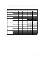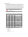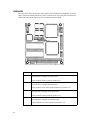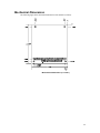
1
CMV586DX133,
CMV486DX100HR and
CMV486DX66HR cpuModuleTM
User’s Manual
BIOS Versions 4.7x
®
USA
Publication CMV586 99.06.03
CMV586DX133, CMV486DX100HR and
CMV486DX66HR cpuModuleTM
User’s Manual
®
USA
REAL TIME DEVICES USA, INC.
200 Innovation Blvd
PO Box 906
State College, PA 16804-0906
Phone: +1-814-234-8087
FAX: +1-814-234-5218
E-mail
[email protected]
[email protected]
website
http://www.rtdusa.com
Revision History
97.09.03
New FM version.
97.09.08
Fixed references to ATSET.
97.09.09
Fixed description of {F1} upon error.
97.10.31
v4.6x initial release
98.02.26
Added CMi586 v4.6x
98.05.20
Added CMC version
98.06.12}
Fixed CMX JP5 and JP6
99.05.11
Fixed Serial Port Disables, bus clock, added quick boot
99.05.25
Fixed parallel port description, separated 386 and 586
99.05.28
Cleaned up numbering and added bottom solder blob WMF
99.06.03
Changed BIOS number
Publication CMV586 99.06.03
Published by:
Real Time Devices USA, Inc.
200 Innovation Blvd.
P.O. Box 906
State College, PA 16804-0906
Copyright 1996, 1997, 1998 by Real Time Devices USA, Inc.
All rights reserved
Printed in U.S.A.
PC/XT, PC/AT are registered trademarks of IBM Corporation.
IBM is a registered trademark of International Business Machines Inc.
MS-DOS is a registered trademark of Microsoft Corp.
PC/104 is a registered trademark of PC/104 Consortium.
The Real Time Devices Logo is a registered trademark of Real Time Devices USA.
cpuModule is a trademark of Real Time Devices USA.
CMV586DX133, CMV486DX100HR and CMV486DX66HR are trademarks of Real Time Devices USA.
utilityModule is a trademark of Real Time Devices USA.
All other trademarks appearing in this document are the property of their respective owners.
Chapter 1: Introduction . . . . . . . . . . . . . . . . . . . . . . . . . . . . . . . . . . 7
The CMV586DX133 / 486DX100HR / 486DX66HR cpuModules .8
Specifications ....................................................................................10
Chapter 2: Getting Started . . . . . . . . . . . . . . . . . . . . . . . . . . . . . . . . 13
Basic Connector Locations ...............................................................14
Default Configuration .......................................................................15
Cable Kits .........................................................................................16
Connecting Power .............................................................................17
Connecting the utility cable ..............................................................18
Connecting a Keyboard ....................................................................19
Connecting to the PC/104 Bus ..........................................................20
Booting the cpuModule for the First Time .......................................21
If You Misconfigure the cpuModule ................................................22
For More Information .......................................................................23
Chapter 3: Connecting the cpuModule . . . . . . . . . . . . . . . . . . . . . . 25
I/O Connections ................................................................................26
Auxiliary Power, J8 ..........................................................................28
First Serial Port, J3 ............................................................................29
Second Serial Port, J4 .......................................................................30
Parallel Port, J2 .................................................................................31
Multifunction Connector, J1 .............................................................33
Chapter 4: Configuring the cpuModule . . . . . . . . . . . . . . . . . . . . . 41
Configuring Hardware ......................................................................42
Configuring with the Setup program ................................................47
Chapter 5: Using the cpuModule . . . . . . . . . . . . . . . . . . . . . . . . . . . 55
The BIOS ..........................................................................................60
BIOS Routines for Hardware Control ..............................................65
Direct Hardware Control ..................................................................70
Storing Applications On-board .........................................................74
Using Virtual Devices .......................................................................83
Utility Programs ................................................................................88
Chapter 6: Hardware Reference . . . . . . . . . . . . . . . . . . . . . . . . . . . 93
Jumpers .............................................................................................94
Solder Jumpers ..................................................................................98
Mechanical Dimensions ....................................................................99
486DX100/66 Processor Thermal Management ..............................100
5x86DX133 Processor Thermal Management .................................101
Chapter 7: Troubleshooting . . . . . . . . . . . . . . . . . . . . . . . . . . . . . . . 103
Common Problems and Solutions .....................................................104
Chapter 8: Limited Warranty . . . . . . . . . . . . . . . . . . . . . . . . . . . . . 111
CHAPTER 1: INTRODUCTION
This manual is meant for users developing with the CMV586DX133,
CMV486DX100HR or CMV486DX66HR cpuModules. It contains information on hardware and software of the cpuModule.
The manual is organized as follows:
Chapter 1:
Introduction
Introduces main features and specifications.
Chapter 2:
Getting Started
Provides abbreviated instructions to get started.
Chapter 3:
Connecting the cpuModule
Provides information on connecting the cpuModule to peripherals.
Chapter 4:
Configuring the cpuModule
Provides information on configuring hardware and software.
Chapter 5:
Using the cpuModule
Provides information needed to develop applications for the cpuModule.
The chapter includes general information on the cpuModule, plus detailed information on storing applications, using Virtual Devices and system functions, and using utility programs.
Chapter 6:
Hardware Reference
Lists jumpers and their locations and mechanical dimensions.
Chapter 7:
Troubleshooting
Offers advice on debugging problems with your system.
Chapter 8:
Warranty
The CMV586DX133 / 486DX100HR / 486DX66HR cpuModules
The PC/104 cpuModules described in this manual are designed for industrial applications which require:
•
software and hardware compatibility with the PC/AT world
•
high-speed "number-crunching" operation
•
low power consumption
•
small physical dimensions
•
high reliability
•
good noise immunity
This cpuModule is highly integrated, combining all major functions of a PC/AT computer on one
compact board. It integrates all primary I/O functions of a AT compatible computer:
•
keyboard interface
•
Bidirectional parallel port
•
two RS232 serial ports
•
Real Time Clock
•
Speaker port
It also enhances standard AT-compatible computer systems by adding:
•
two Solid State Disk sockets
•
a non-volatile configuration EEPROM
•
a Watchdog Timer
The figure below shows a simplified block diagram of the cpuModule:
AMD
486 or 5x86
Processor
8MB
DRAM
EEPROM
RS232
RS232
Parallel
Keyboard
Speaker
BIOS
ACC Micro
Chipset
Watchdog
SSD
Sockets
Bus Buffers
PC/104 Bus
You can easily customize the cpuModule by stacking PC/104 modules such as video controllers,
modems, LAN controllers, or analog and digital data acquisition modules. Stacking PC/104 modules
on the cpuModule avoids expensive installations of backplanes and card cages and preserves the
module's compactness.
8
A PC compatible BIOS is also implemented in the cpuModule. This BIOS supports ROM-DOS and
MS-DOS operating systems. Drivers in the BIOS allow booting from floppy disk, hard disk, Solid
State Disk, or DiskOnChip, thus enabling the system to be used with traditional disk drives or nonmechanical drives.
The cpuModule and BIOS are also compatible with most real-time operating systems for PC compatible computers, although these may require creation of custom drivers to use the SSD, EEPROM,
and watchdog timer.
For industrial applications, a set of BIOS functions have also been implemented which allow easy
control of system hardware devices.
9
Specifications
CMV586DX133
•
•
•
•
•
AMD Am5x86 microprocessor
133 MHz clock speed
3.3 V processor supply
16 KB on-chip cache memory
Math coprocessor
CMV486DX100HR
•
•
•
•
•
•
AMD Am486 microprocessor
100 MHz clock speed
Extended temperature processor
3.3 V processor supply
16 KB on-chip cache memory
Math coprocessor
CMV486DX66HR
•
•
•
•
•
•
AMD Am486 microprocessor
66 MHz clock speed
Extended temperature processor
3.3 V processor supply
16 KB on-chip cache memory
Math coprocessor
DMA, Interrupts, Timers
•
•
•
Six (6) DMA channels (8237 compatible)
Fifteen (15) interrupt channels (8259 compatible)
Three (3) counter/timers (8254 compatible)
Memory Configurations
•
8M bytes DRAM, installed
Solid State Disk
•
•
Device
Atmel 5V Flash
SRAM
NOVRAM
12V Flash
(read-only)
EPROM
AMD 5V Flash
•
10
two 32-pin sockets
an SSD socket can hold one of the following Conventional SSD devices:
Full Read/Write
Access
yes
yes
yes
no
128Kbytes
256Kbytes
512Kbytes
1Mbyte
yes
yes
yes
yes
yes
no
no
yes
yes
yes
yes
no
no
no
no
no
no
no
yes
yes
yes
no
yes
yes
yes
no
an SSD socket can alternately hold one of the following devices which install using a
BIOS Extension:
Device
DiskOnChip 2000
DiskOnChip 1000
MCSI PromDisk
Full Read/Write
Access
yes
yes
yes
Maximum Number per
cpuModule
1
1
2
Sizes
2 - 72 MB *
1MB, 2MB
4MB, 8MB *
(*) Larger devices may be available in the future.
Peripherals
•
•
•
•
•
•
Two full-duplex RS232 serial ports; baud rates from 50 to 115.2k baud
(with 16450-type UARTs)
Parallel port with SPP and bidirectional capability with selectable interrupts
PC/AT standard keyboard port
Speaker port
Real Time Clock (requires user-supplied external battery for backup)
Watchdog Timer
BIOS
•
•
•
•
Directly supports Solid State Disk (SSD) and DiskOnChip
User-configurable using built-in Setup program
Supports serial link to host computer for keyboard, video, floppy, hard disk
Can boot from floppy disk, hard disk, Solid State Disk,
or serial port link (Virtual Devices)
Connections
•
•
•
•
•
•
AT bus, per PC/104 specifications (64-pin J7, 40-pin J6)
Serial port 1 connector (10-pin J3)
Serial port 2 connector (10-pin J4)
Parallel port connector (26-pin J2)
Multifunction connector (10-pin J1)
Auxiliary power connector (8-pin J8)
Physical Characteristics
•
•
•
Dimensions: 3.6 x 3.8 x 0.6" (97 x 100 x 16mm)
Weight (mass): 3.4 ounces (100 grams)
PCB: 12-layer, mixed surface-mount and thru-hole
Operating environment
•
•
•
•
•
Power supply: 5V +/- 5%
486DX100 processor operating temperature: -40 to +85 degrees C (with proper cooling) See 486DX100/66 Processor Thermal Management on page 100
586DX133 processor operating temperature: -20 to +70 degrees C (with proper cooling) See 5x86DX133 Processor Thermal Management on page 101
Operating relative humidity: 0 to 95%, non-condensing
Storage temperature : -55 to +125 degrees C.
Power Consumption
Exact power consumption depends on the peripherals connected to the board, the selected SSD configuration and the memory configuration.
11
The table below lists power consumption for typical configurations and clock speeds:
Typical Power Consumption
Module
Consumption
RAM
SSD
Coprocessor
CMV586DX133
133MHz
1.75A (8.75W)
8MB
512kB
Atmel Flash
Internal
CMV486DX100HR
100MHz
1.5A (7.5W)
8MB
512kB
Atmel Flash
Internal
CMV486DX66HR
67MHz
0.84A (4.2W)
8MB
512kB
Atmel Flash
Internal
For information on changing clock speeds, see Processor Clock Control on page 73.
12
CHAPTER 2: GETTING STARTED
For many users, the factory configuration of the cpuModule can be used
to get a PC/104 system operational. If you are one of these users, you can
get your system up and running quickly by following a few simple steps
described in this chapter. Briefly, these steps are:
• Connect power.
• Connect the utility cable.
• Connect a keyboard.
• Connect the PC/104 bus to a video card.
Refer to the remainder of this chapter for details on each of these steps.
13
Basic Connector Locations
The figure and table below show the connectors used in this chapter.
J1
J7
J6
J8
CMV Basic Connector Locations
Basic Connectors
Connector
Function
Size
J1
Multifunction
10 pin
J6
PC/104 bus (AT)
40 pin
J7
PC/104 Bus (XT)
64 pin
J8
Auxiliary power
10 pin
For a complete listing of connectors, please refer to I/O Connections on page 26.
NOTE!
14
Pin 1 of each connector is indicated by a square solder pad on the bottom of the PC board and a white box silkscreened on the top of the
board.
Default Configuration
The cpuModule comes from the factory with jumper JP5 installed. This forces the cpuModule to use
the default Setup outlined in the following table. This configuration allows you to:
•
boot from the Atmel SSD included in the first SSD socket or from floppy disk
•
run the Setup program to configure the cpuModule
This procedure is described in more detail at the end of this chapter.
Highlights of Default Setup
Item
Setting
Controlled by:
Boot device
Atmel SSD / Floppy
Setup
SSD size/type
Atmel 512KB Flash in
first SSD socket
Setup + jumpers
Memory
8MB
Setup
Video
EGA/VGA
Setup
Floppy Drive 1
1.44M 3.5"
Setup
Floppy Drive 2
Not installed
Setup
Hard disk
Not installed
Setup
15
Cable Kits
For maximum flexibility, cables are not provided with the cpuModule. You may wish to purchase
our cable kit for the cpuModule.
The XK-CM10 cable kit contains the following:
•
•
•
•
16
Multifunction cable (keyboard socket, battery, reset, speaker)
Two serial port cables (two - DIL10 to DSUB9)
Parallel port cable (DIL26 to DSUB25)
Power cable (DIL8 to wire leads)
Connecting Power
WARNING!
If you improperly connect power, the module will almost certainly be
damaged or destroyed. Such damage is not warranted! Please verify
connections to the module before applying power.
Power is normally supplied to the cpuModule through the PC/104 bus, connectors J6 and J7. If you
are placing the cpuModule onto a PC/104 stack that has a power supply, you do not need to make
additional connections to supply power.
If you are using the cpuModule without a PC/104 stack or with a stack that does not include a power
supply, refer to Auxiliary Power, J8 on page 28 for more details.
17
Connecting the utility cable
The Multifunction connector, J1, implements the following interfaces:
•
AT keyboard
•
Speaker output
•
System reset input
•
Battery input
To use these interfaces, you must connect to the Multifunction connector, making sure the orientation of pin 1 is correct. If you are using the Multifunction cable from our cable kit, the cable provides
a small speaker, a 5-pin circular DIN connector for the keyboard, a pushbutton for resetting the PC/
104 system, and a lithium battery to provide backup power to the Real Time Clock.
To connect individual devices to the Multifunction connector, please see Multifunction Connector,
J1 on page 33.
18
Connecting a Keyboard
You may plug a PC/AT compatible keyboard directly into the circular DIN connector of the Multifunction cable in our cable kit. Some newer keyboards may use a smaller "mini-DIN" connector; you
will need an adapter to plug these keyboards into the cpuModule.
NOTE!
Many keyboards are switchable between PC/XT and AT operating
modes, with the mode usually selected by a switch on the back or bottom of the keyboard. For correct operation with this cpuModule, you
must select AT mode.
19
Connecting to the PC/104 Bus
Since this cpuModule does not include a video display controller, you will probably wish to stack
the cpuModule with another card to add video. For example, you may add the CM112 utilityModule,
which adds a VGA display controller with flat-panel support and a floppy and IDE hard drive controller, all on one PC/104 module.
The PC/104 bus connectors of the cpuModule are simply plugged onto a PC/104 stack to connect to
other devices.
We recommend you follow the procedure below to ensure that stacking of the modules does not
damage connectors or electronics.
WARNING!
Do not force the module onto the stack! Wiggling the module or applying too much pressure may damage it. If the module does not readily
press into place, remove it, check for bent pins or out-of-place keying
pins, and try again.
• Turn off power to the PC/104 system or stack.
• Select and install standoffs to properly position the cpuModule on the PC/104 stack.
• Touch a grounded metal part of the rack to discharge any buildup of static electricity.
• Remove the cpuModule from its anti-static bag.
• Check that keying pins in the bus connector are properly positioned.
• Check the stacking order; make sure an XT bus card will not be placed between two
AT bus cards or it will interrupt the AT bus signals.
• Hold the cpuModule by its edges and orient it so the bus connector pins line up with
the matching connector on the stack.
• Gently and evenly press the cpuModule onto the PC/104 stack.
20
Booting the cpuModule for the First Time
You can now apply power to the cpuModule. Depending on the VGA card you are using, you may
see a greeting message from the VGA BIOS. You will then see:
•
•
the cpuModule BIOS version information
a message indicating jumper JP5 is installed and the default Setup is therefore being
used
•
a message requesting you press {F1} to continue booting using the default Setup, or
press {Delete} to enter the Setup program
If you press {F1}, the cpuModule will try to boot from a 512KB Atmel Flash in the first SSD socket.
If no device is found, it will try to boot from the first floppy drive.
If you press {Delete}, the cpuModule will enter Setup. Once you have configured the cpuModule
using Setup, save your changes, turn off power, remove jumper JP5, and reboot.
21
If You Misconfigure the cpuModule
It is possible you may incorrectly configure the cpuModule using Setup. If this happens, you have
several choices:
If video and keyboard are enabled:
• Re-boot the cpuModule.
• Immediately press and hold down the {Delete} key until the cpuModule enters Setup.
If video or keyboard are disabled:
• Insert jumper JP5. This will force the cpuModule to boot using the default configuration, which enables video and keyboard.
• Boot the cpuModule.
• Press the {Delete} key to enter Setup.
If the option <DEL> for Setup is disabled in the Advanced Setup screen:
• Insert jumper JP5. This will force the cpuModule to boot using the default configuration, which enables the {Delete} key to run Setup.
• Boot the cpuModule.
• Press the {Delete} key to enter Setup.
You can then reconfigure the cpuModule correctly using Setup.
22
For More Information
This chapter has been intended to get the typical user up and running quickly. If you need more details, please refer to the following chapters for more information on configuring and using the cpuModule.
23
24
CHAPTER 3: CONNECTING THE CPUMODULE
This chapter contains information necessary to use all connectors of the
cpuModule.
25
I/O Connections
The cpuModule comes from the factory ready to connect to the peripherals shown in the following
table.
Default Peripheral Settings
Item
Setting
Controlled by
Boot device
Atmel SSD / Floppy
Setup
SSD size/type
DiskOnChip @ D000
Setup + jumpers
Serial Port #1
3F8H
Setup
Serial Port #2
disabled
Setup
Parallel Port
Bi-directional at 378H
Setup
Video
EGA/VGA
Setup
Floppy Drive 1
1.44M 3.5"
Setup
Floppy Drive 2
Not installed
Setup
Hard disk
Not installed
Setup
If you are using peripherals compatible with this list, you do not need to configure any jumpers or
software settings before connecting peripherals.
If you are using different peripherals, you may need to change the cpuModule settings. In that case,
please see Configuring with the Setup program on page 47.
26
Connector Locations
The figure and table below show all connectors and the SSD sockets of the cpuModule.
J4
J3
J2
U2
J1
U1
J7
J8
J6
CMV Connector Locations
Connectors
NOTE!
Connector
Function
Size
J1
J2
J3
J4
J6
J7
J8
Multifunction
Parallel port
Serial port #1
Serial port #2
PC/104 bus (AT)
PC/104 bus (XT)
Auxiliary Power
10 pin
26 pin
10 pin
10 pin
40 pin
64 pin
8 pin
Pin 1 of each connector is indicated by a square solder pad on the bottom of the PC board and a white box silkscreened on the top of the
board.
27
Auxiliary Power, J8
WARNING!
If you improperly connect power, the module will almost certainly be
destroyed. Please verify power connections to the module before
applying power.
The power supply can be conveyed to the module either through the PC/104 bus (J6 and J7) or
through the Auxiliary Power connector, J8.
Facing the connector pins, the pinout of the Auxiliary Power connector is:
NOTE!
7
5
3
1
GND
-5V
+5V
-12V
+12V
+5V
8
6
4
2
GND
-5VDC, +12VDC and -12VDC voltages are not used by the module,
but are carried on the PC/104 bus connectors, J6 and J7.
Power Supply Protection
The cpuModule has protection circuitry which helps prevent damage due to problems with the +5V
supply, such as:
•
Reversed polarity
•
Overvoltage
•
Overcurrent
The circuitry includes a user-replaceable fuse, which is located near the PC/104 bus connector. This
fuse is a:
•
•
28
2 amp Nano fuse
Littelfuse part number R451 002
First Serial Port, J3
The first serial port is implemented on connector J3. The serial port is a PC compatible full-duplex
RS232 port.
The I/O address and interrupt for the serial port can be individually selected using Setup. The available I/O addresses and interrupts are shown in the following table.
First Serial Port Settings
I/O Address
Default IRQ
Optional IRQs
03F8H
02F8H
IRQ4
IRQ3
IRQ3, IRQ5
IRQ4, IRQ5
First Serial Port UART
The second serial port is implemented with a 16450-compatible UART (Universal Asynchronous
Receiver/Transmitter). This UART is capable of baud rates up to 115.2 kbaud. Please refer to any
standard PC-AT hardware reference for the register map of the 16450-type UART.
RS232 Serial Port
The second serial port operates only in full-duplex RS232 mode. It must therefore be connected to
an RS232-compatible device.
The following table gives the connector pinout and shows how to connect to an external serial connector, either XT(DB25) or AT(DB 9) compatible.
Pin
1
2
3
4
5
6
7
8
9,10
Connector J3: Pin Assignments in RS232 Mode
Signal
Function
in/out
DB25
DCD
DSR
RX
RTS
TX
CTS
DTR
RI
GND
Data Carrier Detect
Data Set Ready
Receive Data
Request To Send
Transmit data
Clear To Send
Data Terminal Ready
Ring Indicate
Signal Ground
in
in
in
out
out
in
out
in
--
8
6
3
4
2
5
20
22
7
DB9
1
6
2
7
3
8
4
9
5
Facing the connector pins, the pinout is:
9
7
5
3
1
GND
DTR
TXD
RXD
DCD
GND
RI
CTS
RTS
DSR
10
8
6
4
2
29
Second Serial Port, J4
A second serial port is implemented on connector J4. The serial port is a PC compatible full-duplex
RS232 port.
The I/O address and interrupt for the serial port are individually selected using Setup. The available
I/O addresses and interrupts are shown in the following table.
Second Serial Port Settings
I/O Address
Default IRQ
Optional IRQs
02F8H
02E8H
IRQ4
IRQ3
IRQ3, IRQ5
IRQ4, IRQ5
Second Serial Port UART
The second serial port is implemented with a 16450-compatible UART (Universal Asynchronous
Receiver/Transmitter). This UART is capable of baud rates up to 115.2 kbaud. Please refer to any
standard PC-AT hardware reference for the register map of the 16450-type UART.
RS232 Serial Port
The second serial port operates only in full-duplex RS232 mode. It must therefore be connected to
an RS232-compatible device.
The following table gives the connector pinout and shows how to connect to an external serial connector, either XT(DB25) or AT(DB 9) compatible.
Pin
1
2
3
4
5
6
7
8
9,10
Connector J4: Pin Assignments in RS232 Mode
Signal
Function
in/out
DB25
DCD
DSR
RX
RTS
TX
CTS
DTR
RI
GND
Data Carrier Detect
Data Set Ready
Receive Data
Request To Send
Transmit data
Clear To Send
Data Terminal Ready
Ring Indicate
Signal Ground
in
in
in
out
out
in
out
in
--
8
6
3
4
2
5
20
22
7
DB9
1
6
2
7
3
8
4
9
5
Facing the connector pins, the pinout is:
30
9
7
5
3
1
GND
DTR
TXD
RXD
DCD
GND
RI
CTS
RTS
DSR
10
8
6
4
2
Parallel Port, J2
The parallel port is available on connector J2. You can use Setup to select its address and associated
interrupt.
The pinout of the connector allows a ribbon cable to directly connect it to a DB25 connector, thus
providing a standard PC compatible port.
The following tables lists the parallel port signals and explains how to connect it to a DB25 connector to obtain a PC compatible port.
NOTE!
For correct operation, keep the length of the cable connecting the cpuModule and parallel device less than 3 meters (10 feet).
Parallel Port Connector, J2
Pin
Signal
Function
in/out
DB25
1
STB
Strobe Data
out
1
2
AFD
Autofeed
out
14
3
PD0
Printer Data 0 (LSB)
out
2
4
ERR
Printer Error
in
15
5
PD1
Parallel Data 1
out
3
6
INIT
Initialize printer
out
16
7
PD2
Printer Data 2
out
4
8
SLIN
Select printer
out
17
9
PD3
Printer Data 3
out
5
10
GND
Signal ground
--
18
11
PD4
Printer Data 4
out
6
12
GND
Signal ground
--
19
13
PD5
Printer Data 5
out
7
14
GND
Signal ground
--
20
15
PD6
Printer Data 6
out
8
16
GND
Signal ground
--
21
17
PD7
Printer Data 7 (MSB)
out
9
18
GND
Signal ground
--
22
19
ACK
Acknowledge
in
10
20
GND
Signal ground
--
23
31
32
21
BSY
Busy
in
11
22
GND
Signal ground
--
24
23
PE
Paper End
in
12
24
GND
Signal ground
--
25
25
SLCT
Ready To Receive
in
13
26
GND
Signal ground
--
26
Multifunction Connector, J1
The Multifunction connector on J1 implements the following functions:
•
Speaker output
•
AT keyboard
•
System reset input
•
Watchdog Timer output
•
Battery Input
•
Programming voltage input
The following table gives the pinout of the Multifunction connector.
Pin
Multifunction Connector, J1
Signal
Function
1
2
3
4
5
6
7
8
9
10
SPKR+
SPKRRESET
WD
KBD
KBC
GND
KBP
BAT
Vpp
in/out
Speaker output
Speaker output
External reset
Watchdog output
Keyboard Data
Keyboard Clock
Ground
Keyboard Power
Battery input
Vpp for programming
out
out
in
out
in
out
-out
in
in
Facing the connector pins, the pinout is:
9
7
5
3
1
BAT
GND
KBD
RESET
SPKR+
Vpp
KBP
KBC
WD
SPKR-
10
8
6
4
2
Speaker
A speaker output is available on two pins of the Multifunction connector. These outputs are controlled by a transistor to supply 0.1 watt of power to an external speaker. The external speaker should
have 8 ohm impedance.
Keyboard
An AT compatible keyboard can be connected to the Multifunction connector. Usually PC keyboards come with a cable ending with a 5-pin male ’DIN’ connector. The following table lists the
relationship between the Multifunction connector pins and a standard ’DIN’ keyboard connector.
33
To ensure correct operation, check that the keyboard is either an AT compatible keyboard or a switchable XT/AT keyboard set to AT mode. Switchable keyboards are usually set by a switch on the
back or bottom of the keyboard.
Pin
5
6
7
8
Keyboard Connector
Signal
Function
KBD
KBC
GND
KBP
Keyboard Data
Keyboard Clock
Ground
Keyboard Power
DIN
2
1
4
5
System Reset
Pin 3 of the multifunction connector allows connection of an external pushbutton to manually reset
the system. The pushbutton should be normally open, and connect to ground when pushed.
Watchdog Timer
The active-high Watchdog signal generated on the cpuModule is available on pin 4 of the multifunction connector.The Watchdog time-out period is 1.2 seconds. If the Watchdog timer is not reset within that period, it the Watchdog signal is asserted and the cpuModule is reset.
See Watchdog Timer Control on page 69 for more information on controlling the Watchdog Timer.
Battery
Pin 9 of the multifunction connector is the connection for an external backup battery (in the range
2.40V to 4.15V; typically 3.6V). This battery is used by the cpuModule when system power is removed, to:
•
preserve the date and time in the Real Time Clock
•
preserve information stored in Static RAM in the Solid State Disk
If you wish to back-up Static RAMs in the Solid State Disk, please note that:
•
•
jumpers JP2 and JP4 must be correctly set;
see Storing Applications On-board on page 74
SSD backup requires considerable battery power;
you may require a larger backup battery than supplied with the cable kit
Programming Voltage, Vpp
Pin 10 of the Multifunction connector is used when programming 12 volt Flash EPROMs in the
SSD, or when reprogramming the BIOS. You must supply this pin with a programming voltage,
Vpp, of 12VDC +/- 5% to program these devices.
34
Refer to Storing Applications On-board on page 74 and BIOS Build Utility (BIOSBLD.EXE) on
page 91 for more information.
NOTE!
Once programming voltage is applied to pin 10 of the Multifunction
connector, it still must be enabled to the individual SSD sockets:
Jumper JP1 pins 5-6 enable programming voltage to SSD socket U1.
Jumper JP3 pins 5-6 enable programming voltage to SSD socket U2.
PC/104 Bus, J6 and J7Connectors J6 and J7 carry signals of the PC/104 bus;
these signals match definitions of the IEEE P996 standard. The following tables list the pinouts of
the PC/104 bus connectors.
The following table lists the signals of the XT portion of the PC/104 bus.
Pin
1
2
3
4
5
6
7
8
9
10
11
12
13
14
15
16
17
18
19
20
21
22
23
24
25
26
27
28
PC/104 XT Bus Connector, J7
Row A
N.C.
SD7
SD6
SD5
SD4
SD3
SD2
SD1
SD0
IOCHRDY
AEN
SA19
SA18
SA17
SA16
SA15
SA14
SA13
SA12
SA11
SA10
SA9
SA8
SA7
SA6
SA5
SA4
SA3
Row B
0V
RESETDRV
+5V
IRQ2
-5V
DRQ2
-12V
N.C.
+12V
(Keying pin)
SMEMW*
SMEMR*
IOW*
IOR*
DACK3*
DRQ3
DACK1*
DRQ1
REFRESH*
SYSCLK
IRQ7
IRQ6
IRQ5
IRQ4
IRQ3
DACK2*
TC
BALE
35
29
30
31
32
36
SA2
SA1
SA0
0V
+5V
OSC
0V
0V
The following table lists signals of the AT portion of the PC/104 bus.
PC/104 AT Bus Connector, J6
Pin
Row C
Row D
1
0V
0V
2
SBHE*
MEMCS16*
3
LA23
IOCS16*
4
LA22
IRQ10
5
LA21
IRQ11
6
LA20
IRQ12
7
LA19
IRQ15
8
LA18
IRQ14
9
LA17
DACK0*
10
MEMR*
DRQ0
11
MEMW*
DACK5*
12
SD8
DRQ5
13
SD9
DACK6*
14
SD10
DRQ6
15
SD11
DACK7*
16
SD12
DRQ7
17
SD13
+5V*
18
SD14
MASTER*
19
SD15
0V
20
(Keying pin)
0V
Notes:
Keying pin positions are blanked to prevent misalignment of stacked modules. This is a feature of
the PC/104 specification and should be implemented on all mating PC/104 modules.
Signals marked with (*) are active-low.
All bus lines can drive a maximum current of 6mA at TTL voltage levels.
37
PC/104 Bus Signals
The following table contains brief descriptions of the PC/104 bus signals.
Signal
I/O
Description
AEN
O
Address ENable: when this line is active (high), it means a DMA
transfer is being performed and therefore the DMA controller has control over the data bus, the address bus, and the control lines.
BALE
O
Bus Address Latch Enable, active high. When active, it indicates that
address lines SA0 to SA19 are valid.
DACKx*
O
DMA ACKnowledge x=0-7, active low, used to acknowledge DMA
requests.
DRQx
I
DMA Request x=0-7: these are asynchronous lines used by peripheral
devices to request DMA service. They have increasing priority from
DRQ0 up to DRQ7. A DMA request is performed by setting the DRQ
line high and keeping it high until the corresponding DACK line is activated.
ENDXFR*
I/O
This is the only synchronous signal of the PC/104 bus and it is active
low. It indicates that the current bus cycle must be performed with 0
wait states. It is used only for 16-bit boards.
IOCHCHK*
I
I/O Channel Check, active low, indicates an error condition that cannot be corrected.
IOCHRDY
I
I/O Channel Ready: this line, usually high (ready) is pulled to a low
level by devices which need longer bus cycles.
IOCS16*
I
I/O Chip Select 16-bit: this line, active low, is controlled by devices
mapped in the I/O address space. It indicates they have a 16-bit bus
width.
IOR*
O
I/O Read, active low, indicates when the devices present on the bus
can send their information on the data bus.
IOW*
O
I/O Write, active low. When active, it allows the peripheral devices to
read data present on the data bus.
IRQx
I
Interrupt Request: x = 2 to 15, active on rising edge. IRQ15 has top
priority; the other lines have decreasing priority starting from IRQ14
down to IRQ2. An interrupt request is performed by changing the level of the corresponding line from low to high and keeping it high until
the microprocessor has recognised it.
KEY
N/A
These locations contain mechanical keying pins to help prevent incorrect connector insertion.
O
These signals select a 128kbyte window in the 16Mbyte address space
available on the bus.
LA23..LA17
38
MASTER*
I
During a DMA cycle, this active-low signal, indicates that a resource
on the bus is about to drive the data and address lines.
MEMCS16*
I
Memory Chip Select 16-bit: this line, active low, is controlled by devices mapped in the memory address space and indicates they have a
16-bit bus width.
MEMR*
I/O
This active-low signal indicates a memory read operation. Devices using this signal must decode the address on lines LA23..LA17 and
SA19..SA0.
MEMW*
I/O
This active-low signal indicates a memory write operation. Devices
using this signal must decode the address on lines LA23..LA17 and
SA19..SA0.
OSC
O
OSCillator: clock with a 70 ns period and a 50% duty cycle. It is a
14.31818MHz always presents.
REFRESH*
O
This line is active low and indicates that the current bus cycle is a
DRAM refresh cycle. The refresh cycles are activated every 15 microseconds.
RESETDRV
O
This line, active high, is used to reset the devices on the bus, at poweron or after a reset command.
SA0..19
O
Address bits 0 to 19: these lines are used to address the memory space
and the I/O space. SA0 is the least significant bit while SA19 is the
most significant bit.
SBHE*
O
This active-low signal indicates a transfer of the most significant data
byte (SD15..SD8).
SD8..15
I/O
Data bits: these are the high-byte data bus lines. SD8 is the least significant bit; SD15 the most significant bit.
SD0..7
I/O
Data bits: these are the low-byte data bus lines. SD0 is the least significant bit; SD7 the most significant bit.
SMEMR*
O
Memory Read command, active low.
SMEMW*
O
Memory Write command, active low.
SYSCLK
O
System Clock, 8.0MHz with a 50% duty cycle. Only driven during external bus cycles.
TC
O
Terminal Count: this line is active high and indicates the conclusion
of a DMA transfer.
39
PC/104 Bus Termination
Termination of PC/104 bus signals is not recommended and may cause malfunctions of the cpuModule. If termination must be applied, it should be a series termination of a resistor and capacitor, not
exceeding 40-60 ohms and 30-70 pF, between each signal and ground.
40
CHAPTER 4: CONFIGURING THE CPUMODULE
This chapter contains information to configure the cpuModule.
Topics covered in this chapter include:
• Configuration jumpers
• Adding SSD Memory
• Configuring Using the Setup Program
41
Configuring Hardware
42
Jumpers
Many cpuModule options are configured by positioning jumpers. Jumpers are labeled on the board
as “JP” followed by a number.
Some jumpers are three pins, allowing three settings:
•
•
•
pins 1 and 2 connected (indicated as "1-2")
pins 2 and 3 connected (indicated as "2-3")
no pins connected.
1
2
3
Some jumpers are two-pin, allowing two settings:
•
•
pins 1 and 2 connected (indicated as "closed")
pins 1 and 2 un-connected (indicated as "open")
1
2
Other jumpers are six-pin, allowing pins to be connected in one of three pairs:
•
•
•
pins 1 and 2 connected (indicated as "1-2")
pins 3 and 4 connected (indicated as "3-4")
pins 5 and 6 connected (indicated as "5-6")
2
4
6
1
3
5
Six pin jumpers on this cpuModule do not use other positions, such as 1-3, 3-5, 2-4, or 4-6.
43
Installing SSD Memory
This section explains how to add devices to the cpuModule. This procedure is only necessary when
you wish to add or change:
•
Solid State Disk memory devices
Installing SSD Memory
You may wish to install SSD memory to use the cpuModule as a "diskless" stand-alone device.
Refer to Ways to Use the Solid State Disk Sockets on page 75 for more information on various SSD
device types. Solid State Disk memories are placed in sockets U1 and U2. Generally, the device type
and size in the first socket do not have to match the device type and size in the second socket.
When implementing the Solid State Disk, you must always follow these rules:
•
•
•
•
44
The first socket must be filled before the second socket can be used;
When using two SRAMs or two NOVRAMs, both devices must be the same size;
When using both a Conventional SSD and a BIOS Extension device in the cpuModule,
the Conventional SSD must go into the first socket;
Generally, only one BIOS Extension device (like M-System's DiskOnChip or MCSI
PromDisk) may be used at a time.
The following table lists possible configurations for the first socket of the SSD and the corresponding jumpers which must be set:
Jumpers for First SSD Socket, CMV586DX133, CMV486DX100HR or CMV486DX66HR
Type
Part
Operation
Capacity
JP1
JP2
Atmel 5V Flash
29C010A
29C040A
DiskOnChip and
PromDisk
read/write
read/write
read/write
128KB
512KB
to 12MB+
1-2
1-2
3-4
1-2
1-2
1-2
DS1645Y
DS1650Y
128KB
read/write
read/write
read/write
128KB
512KB
128KB
512KB
read/write
512KB
28F010
read-only
128KB
28F020
read-only
256KB
29F010
read-only
128KB
3-4
1-2
3-4
3-4
1-2
1-2
5-6
3-4
5-6
3-4
1-2
1-2
1-2
1-2
2-3
1-2
2-3
1-2
1-2
1-2
1-2
1-2
29F040
read-only
512KB
1-2
1-2
27C010
27C020
27C040
27C080
read-only
read-only
read-only
read-only
128KB
256KB
512KB
1MB
3-4
3-4
3-4
1-2
1-2
1-2
1-2
1-2
BIOS Extension
Devices
NOVRAM
SRAM
12V Flash
AMD 5V Flash
EPROM
Notes
no backup
battery backup
no backup
battery backup
programming
read-only
programming
read-only
program or
read
program or
read
45
The following table lists possible configurations for the second socket of the SSD and the corresponding jumpers which must be set:
Jumpers for Second SSD Socket, U2
Type
Part
Operation
Capacity
JP3
JP4
Atmel 5V Flash
29C010A
29C040A
DiskOnChip and
PromDisk
read/write
read/write
read/write
128KB
512KB
to 12MB+
1-2
1-2
3-4
1-2
1-2
1-2
DS1645Y
DS1650Y
128KB
read/write
read/write
read/write
128KB
512KB
128KB
512KB
read/write
512KB
28F010
read-only
128KB
28F020
read-only
256KB
29F010
read-only
128KB
3-4
1-2
3-4
3-4
1-2
1-2
5-6
3-4
5-6
3-4
1-2
1-2
1-2
1-2
2-3
1-2
2-3
1-2
1-2
1-2
1-2
1-2
29F040
read-only
512KB
1-2
1-2
27C010
27C020
27C040
27C080
read-only
read-only
read-only
read-only
128KB
256KB
512KB
1MB
3-4
3-4
3-4
1-2
1-2
1-2
1-2
1-2
BIOS Extension
Devices
NOVRAM
SRAM
12V Flash
AMD 5V Flash
EPROM
46
Notes
no backup
battery backup
no backup
battery backup
programming
read-only
programming
read-only
program or
read
program or
read
Configuring with the Setup program
The cpuModule Setup program allows you to customize the cpuModule's configuration. Selections
made in Setup are stored on the board and read by the BIOS at power-on.
Setup for this cpuModule is called AT486. It is in three places:
•
In the board's BIOS ROM, activated by the {Delete} key during boot
•
In the Utility SSD provided in the first SSD socket
•
On the utility disk supplied with the cpuModule.
The following section explains how to start Setup.
Starting Setup
You can run Setup one of several ways:
• Re-boot the cpuModule, and hold down the {Delete} key.
• Install default jumper JP5, boot the cpuModule, and press the {Delete} key.
• Boot the cpuModule, change to the Utility SSD, and run AT486.EXE.
• Boot the cpuModule, change to a diskette containing AT486.EXE, and run AT486.
When you are finished with Setup, save your changes and exit. If you are using Setup from the BIOS,
the system will automatically reboot. Otherwise, you must manually do a hard reset, by pushing the
reset pushbutton or cycling power.
If jumper JP5 was installed, make sure you turn off the cpuModule, remove the jumper, and reboot
so the changes are recognized.
Using the Setup Program
All displays in Setup consist of two areas. The upper area lists the available selections. The lower
area displays help messages which you should always read.
Main Menu Options
From the Main menu, you may choose:
•
Standard Setup to access commonly used settings for the keyboard, floppy drives, hard
disks, and SSD.
•
Advanced Setup to access less-used settings for memory, the SSD, and error-handling.
•
Save Changes and Exit to save your changes and exit Setup.
•
Exit Without Saving Changes to leave Setup without saving your changes.
Normally you will use the first two selections to make changes to the cpuModule configuration, then
use the Save Changes and Exit selection.
The version of Setup in the BIOS ROM will automatically cause a hard reset after you exit.
The DOS version of Setup (in the utility SSD and on floppy disk) has two added options:
•
Read settings from a File which reads settings from a file on a disk
•
Save Settings to a File which saves settings to a file on disk
These allow users to configure large numbers of modules without manually entering the settings
each time.
The following sections describe each of these choices in detail.
47
Field Selection
You move between fields in Setup using the keys listed below.
Setup Keys
Key
Function
Ð
Ï
{TAB}
selects next field
selects previous field
Î
Í
selects next field on the right or first field of next line
{ESC}
returns to main menu
selects next value in field
selects former value in field
Standard Setup Fields
The following is an alphabetical list of Standard Setup fields.
Standard Setup Fields
Field
Boot Device
Active keys
ÍÎ
Selections
Selects the primary boot device.
Possible selections:
• Floppy Disk
• SSD (Solid State Disk)
• Hard Disk
•
•
Date
{0..9},{↵}
Sets the date with the format:
• month / day / year
• You must connect a backup battery, or this
setting will be lost at power down.
Hard disk 1 type
{0..9} {↵}
Selects the first hard disk type.
Selections are:
• Not Installed
• Standard : (drives under 1024 Cylinders)
• LBA: (drives over 1024 Cylinders)
• Serial: for Virtual Devices mode.
Hard disk 1 table
•
•
48
This selects the device from which system
boot is first attempted.
Hard Disk is used to boot from Hard Disk or
a BIOS Extension device in an SSD socket.
When using Standard, manually enter parameters under Hard Disk 1 Table.
When using LBA, first select Standard, enter
parameters under Hard Disk 1 Table, then
change to LBA. New parameters will be calculated automatically.
Hard disk 2 type
ÍÎ
{0..9} {↵}
Hard disk 2 table
Selects the second hard disk type. Selections are:
• Not Installed
• Standard: (drives under 1024 Cylinders)
• LBA: (drives over 1024 Cylinders)
•
•
Floppy Disk 1
ÍÎ
Floppy Disk 2
ÍÎ
Serial Port J3
ÍÎ
Serial Port J4
ÍÎ
Keyboard
ÍÎ
When using Standard, manually enter parameters under Hard Disk 2 Table.
When using LBA, first select Standard, enter
parameters under Hard Disk 2 Table, then
change to LBA. New parameters will be calculated automatically.
Selects the format of floppy disk 1:
Selections are:
•
360KB
•
720KB
•
1.2MB
•
1.44MB
•
Serial (Used in Virtual Devices mode)
Selects the format of floppy disk 2:
Selections are:
•
360KB
•
720KB
•
1.2MB
•
1.44M
Selects the address and type of the first serial port.
Selections are:
• RS232 at 03F8H (default)
• RS232 at 02F8H
• RS232 at 03E8H
• RS232 at 02E8H
• Disabled
Selects the address of the second serial port.
Selections are:
• 03F8H
• 02F8H (default)
• 03E8H
• 02E8H
• Virtual Devices
• Disabled
Selects the keyboard mode.
Selections are:
•
Disabled
•
ATkey: AT keyboard present
• Serial (Used in Virtual Devices mode)
49
ÍÎ
Memory Size
Selects the size of installed dynamic RAM
(DRAM).
• Selections are4 Mbytes
• 8 Mbytes (standard)
Selecting an incorrect value may cause malfunctions.
ÍÎ
Parallel Port
Time
Selects parallel port address
Selections are:
•
378h (default)
•
278h
•
Disabled
{0...9},{↵}
Sets the time with the format:
• hours : minutes : seconds
You must connect a backup battery or this setting
will be lost at power down.
ÍÎ
Video State
Selects video mode.
Selections are:
•
Monochrome
•
CGA, 40 by 25
•
CGA, 80 by 25
•
EGA/VGA
•
Serial (Used in Virtual Devices mode)
•
Not Installed
Selecting 'Not Installed' will not prevent accesses
to the video controller, which may cause unpredictable results.
Advanced Setup Fields
The following is a list of Advanced Setup fields.
Advanced Setup Fields
Field
SSD Device in
U1
Active keys
ÍÎ
Selections
Selects the device type installed in the first SSD
socket.
•
•
50
The setting here must match the actual device
installed in the socket.
Jumpers JP1 and JP2 must be set correctly.
SSD Device in
U2
ÍÎ
Selects the device type installed in the second SSD
socket.
•
SSD Window
ÍÎ
IRQ3 Source
ÍÎ
IRQ4 Source
ÍÎ
IRQ5 Source
ÍÎ
IRQ7 Source
ÍÎ
•
The setting here must match the actual device
installed in the socket.
Jumpers JP3 and JP4 must be set correctly.
Selects the 32Kbyte address range where the SSD is
mapped.
Selections are:
• D0000H to D7FFFH
• D8000H to DFFFFH
• E0000H to E7FFFH
• E8000H to EFFFFH
When selecting the address range, you must ensure
that:
• no other devices are mapped to the same memory addresses
• shadow memory is not enabled at the same
memory addresses
• selection does not conflict with selection of
BIOS EXT@D000 / D800 / E000 / E800
Determines source for IRQ3 interrupt.
• Disabled
• Serial J3
• Serial J4 (default)
If set to disabled, IRQ3 may be an input from the
PC/104 bus.
Determines source for IRQ4 interrupt.
• Disabled
• Serial J3 (default)
• Serial J4
If set to disabled, IRQ4 may be an input from the
PC/104 bus.
Determines source for IRQ5 interrupt.
• Disabled (default)
• Serial J3
• LPT
If set to disabled, IRQ5 may be an input from the
PC/104 bus.
Determines source for IRQ7 interrupt.
• Disabled
• LPT (default)
• Serial J4
If set to disabled, IRQ7 may be an input from the
PC/104 bus.
51
Shadow C000hC7FFh
ÍÎ
Shadow C800CFFFH
Shadow D000DFFFh
Segment E000h
Map
ÍÎ
Enables shadowing of the BIOS and memory.
Selections are:
• Enabled: address range is copied (shadowed) to
RAM.
• Disabled: address range remains mapped on the
bus.
In DOS systems, addresses between A0000H and
FFFFFH are usually reserved for devices mapped
on the bus. Accesses to these addresses are slower
than accesses to system memory (RAM). The shadow options copy code from these addresses into
RAM, improving general performance of the system.
Selects mapping of segment E000h of memory.
Selections are:
• PC/104 Bus
• BIOS ROM
When PC/104 Bus is selected, addresses in segment
E0000-EFFFFh are free for external use.
52
Boot Type
ÍÎ
Chipset Error
ÍÎ
Memory error
ÍÎ
Video Error
ÍÎ
Keyboard Error
ÍÎ
When BIOS ROM is selected, this segment is
mapped into the on-board BIOS ROM chip.This selection will cause Setup to be executed at every
boot, whether or not {Delete} is pressed.
Selects boot type.
Selections are:
• Standard: Will perform RAM scan/checking
• Quick: Will skip RAM scan/checking
Defines reaction to errors in microprocessor, coprocessor, timer, or DMA and interrupt controller initialization.
ON: prints error warning
OFF: continue without warning
Defines reaction to errors during memory tests.
ON: prints error warning
OFF: continue without warning
This setting only applies during the following power-on tests:
• memory size (base and extended)
• memory test (base and extended)
Defines reaction to video initialization errors:
ON: prints error warning
OFF: continue without warning
Defines reaction to keyboard initialization errors.
ON: prints error warning
OFF: continue without warning
Floppy Error
ÍÎ
Hard Disk Error
ÍÎ
RTC Error
ÍÎ
Defines reaction to floppy drive errors.
ON: prints error warning
OFF: continue without warning
Defines reaction to hard disk errors.
ON: prints error warning
OFF: continue without warning
Defines reaction to Real Time Clock initialization
errors.
ON: prints error warning
OFF: continue without warning
•
Clock/Bus Speed
<DEL> for Setup
ÍÎ
ÍÎ
•
•
•
•
•
When off is selected, the time and date default
to 00:00:00 and 01/01/1990 in case of an error
33.3 (default for 100 or 133 MHz operation)
25
20
15
10
Determines whether pressing the {Delete} key during boot will run the Setup program.
• Enable
• Disable
•
•
In some cases it may be desirable to disable this
feature.
To re-enable the {Delete} key, insert JP5 and
re-boot the cpuModule, then change this setting.
Save Changes and Exit
If you select this menu item, your changes are stored on the cpuModule. If you were running Setup
from the BIOS ROM, the cpuModule automatically reboots. Changes will become effective the next
time the cpuModule boots, as long as jumper JP5 is removed.
Exit Without Saving Changes
If you select this menu item, your changes are not stored on the cpuModule. If you were running
Setup from the BIOS ROM, the cpuModule automatically reboots. Nothing in the cpuModule configuration will be changed, even after the reboot.
Read Settings from a File
If you select this menu item, you are prompted for a file which contains settings to be loaded. The
settings will not be saved to the board unless you select Save Changes and Exit.
53
Save Settings to a File
If you select this menu item, you are prompted for the name of a file to which settings will be saved
(a file name with extension). These settings may be moved to another cpuModule, or used to configure a number of cpuModules identically.
54
CHAPTER 5: USING THE CPUMODULE
This chapter provides information for users who wish to develop their
own applications programs for the cpuModule.
This chapter includes information on the following topics:
• Memory map
• I/O Address map
• Interrupts
• Power On Self Tests (POSTs)
• System Functions (EEPROM, Watchdog Timer, Real Time Clock)
• Virtual Devices
• Storing Applications in Solid State Disk
• Utility Programs (SSD and BIOSBLD)
55
Memory Map
The module addresses memory using 24 address lines. This allows a maximum of 224 locations, or
16 Megabytes of memory.
The table below shows how memory in the first megabyte is allocated in the system.
First Megabyte Memory Map
FFFFFHF0000H
BIOS in Flash EPROM
EFFFFHE0000H
User memory space which normally contains the Setup program. The Advanced Setup screen allows this segment to be
mapped into the BIOS ROM or onto the PC/104 bus.
DFFFFHC0000H
User memory space. Usually, memory between C0000H and
C7FFFH is used for the BIOS of add-on VGA video cards.
BFFFFHA0000H
Normally used for video RAM as follows:
CGA
EGA/VGA
Monochrome
0B8000H to 0BFFFFH
0A0000H to 0AFFFFH
0B0000H to 0B7FFFH
9FFFFH00502H
DOS reserved memory area
00501H00400H
BIOS data area
003FFH00000H
Interrupt vector area
Memory beyond the first megabyte can be accessed in protected mode, by using EMS or a similar
memory manager. See your OS or programming language references for information on memory
managers.
56
Input/Output Address Map
As with all standard PC/104 boards, the Input/Output (I/O) space is addressed by 10 address lines
(SA0-SA9). This allows 210 or 1024 distinct I/O addresses. Any add-on modules you install must
therefore use I/O addresses in the range 0-1024 (decimal) or 000-FFF (hex).
If you add any PC/104 modules or other peripherals to the system you
must ensure they do not use reserved addresses listed below, or malfunctions will occur.
The table below lists I/O addresses reserved for the cpuModule.
I/O Addresses Reserved for the cpuModule
Address Range
Bytes
Device
000H-00FH
16
DMA Controller
010H-01FH
16
Reserved for CPU
020H-021H
2
Interrupt Controller #1
022H-02FH
13
Reserved
040H-043H
4
Timer
060H-064H
5
Keyboard Interface
070H-071H
2
Real Time Clock port
080H-08FH
16
DMA page register
0A0H-0A1H
2
Interrupt controller #2
0C0H-0DFH
32
DMA controller #2
0F0H-0FFH
16
Math co-processor
1F0H-1FFH
16
Hard disk 1
2F8H-2FFH
8
Serial port 2
378H-37FH
8
Parallel port 3
3BCH-3BFH
4
Parallel port 3
3E8H-3EFH
8
Serial port 2
3F0H-3F7H
8
Floppy disk 1
3F8H-3FFH
8
Serial port 2
1
If the floppy and/or hard drive controllers are disabled, the I/O addresses listed will not be occupied.
57
2
Only one of the I/O addresses shown for a Serial port is active at any time. You can use Setup to
select which one is active or to disable it entirely.
3
Only one of the I/O addresses shown for the Parallel printer port is active at any time. You can use
Setup to select which one is active or to disable it entirely.
58
Hardware Interrupts
If you add any PC/104 modules or other peripherals to the system you
must ensure they do not use interrupts needed by the cpuModule, or
malfunctions will occur
The cpuModule supports the standard PC interrupts listed below. Interrupts not in use by hardware
on the cpuModule itself are listed as 'available'.
Hardware Interrupts Used on the cpuModule
Interrupt
Normal Use
Source
0
Timer 0
ACC chipset
1
Keyboard
ACC chipset
2
Cascade of IRQ 8-15
ACC chipset
3
COM2
ACC chipset
4
COM1
ACC chipset
5
available
XT bus
6
Floppy 1
XT bus
7
Printer
ACC chipset
8
Real Time Clock
ACC chipset
9
available
XT bus
10
available
AT bus
11
available
AT bus
12
Not available
ACC chipset
14
IDE hard disk 2
AT bus
15
available
ACC chipset
1
Floppy disk interrupt, INT6, is available for use if no floppy disk is present in the system and floppy disk is disabled in Setup.
2
Hard disk interrupt, INT14, is available for use if no hard disk drive is present in the system and
hard disk is disabled in Setup.
59
The BIOS
The BIOS (Basic Input/Output System) is software that interfaces hardware-specific features of the
cpuModule to an operating system (OS). Physically, the BIOS software is stored in a Flash EPROM
on the cpuModule. Functions of the BIOS are divided into two parts:
The first part of the BIOS is known as POST (Power-On Self-Test) software, and it is active from
the time power is applied until an OS boots (begins execution). POST software performs a series of
hardware tests, sets up the machine as defined in Setup, and begins the boot of the OS;
The second part of the BIOS is known as the CORE BIOS. It is the normal interface between cpuModule hardware and the operating system which is in control. It is active from the time the OS
boots until the cpuModule is turned off. The CORE BIOS provides the system with a series of software interrupts to control various hardware devices.
The following sections discuss the sections of the BIOS in more detail and describe features of the
BIOS which may be useful to you in developing applications.
60
Power On Self Tests (POSTs)
When you turn on system power, the BIOS performs a series of tests and initializations. Each test or
initialization step is identified by a numeric "POST" code written to I/O address 378H. These codes
can be displayed using a commercially available "POST code display board". The following table
lists the POST codes expressed in hexadecimal, with their corresponding meanings.
Code
00H
01H
02H
03H
04H
05H
06H
07H
08H
09H
0AH
0BH
0CH
0DH
0EH
0FH
10H
11H
12H
13H
14H
15H
16H
17H
18H
19H
1AH
1BH
1CH
1DH
1EH
1FH
20H
21H
22H
POST code list
Meaning
CPU validation
CPU test
Component default programming
Timer initialization
Refresh line test
BIOS EPROM test
Keyboard controller test
First 64K RAM test
EEPROM test
0F0000H-0FFFFFH shadow memory test
DMA and interrupt controller initializations
Video device test
Timer #2 test
DMA controller #1 test
DMA controller #2 test
DMA page control registers test
Interrupt controller #1 test
Interrupt controller #2 test
Shutdown byte test
Interrupt line 0 test
Keyboard test
Protected-mode switch test
Base memory size
Expanded memory size
Base memory test
Expanded memory test
Co-processor test
Real Time Clock test
IRQ line test
Parallel port test
Floppy disk test
Hard disk test
Serial port test
Mouse test
Shadow RAM test
61
Errors While Booting
If an error occurs while the system is booting and performing the Power On Self Tests, the system
will respond in one of several ways. Its response depends on what type of error occurred and on certain selections made in Setup.
Any error encountered in POST 1 through 7 causes the module to halt.
Errors encountered after POST 7 are dealt with according to settings made in Setup:
•
With an error set to OFF in the Setup, a message is displayed on the screen and the
speaker beeps. The boot continues if possible.
•
With an error set to ON in the Setup, a message is displayed on the screen (if possible)
and you are asked for confirmation before the boot continues.
If an error is detected in the EEPROM test (POST code 8) the system sets itself according to the default configuration presented in the following section. In that case, the system displays the detected
errors and waits for confirmation before the boot continues.
When an error occurs and you are asked for confirmation to continue the boot, the {F1} key must be
pressed to continue.
62
Default Configuration
In addition to the Setup configuration stored on the board, the cpuModule has a permanent default
configuration. The system will resort to using this default configuration in two situations:
•
An error occurs when accessing the EEPROM which holds the Setup on the module.
•
You force use of the default configuration, as explained in the following section.
The default configuration is listed below.
BIOS Default Configuration
Function
Default selection
Chipset error
Hard disk 1
Hard disk 2
Boot device
Floppy Drive 1
Floppy Drive 2
Floppy Error
Hard disk Error
Serial port 1
Serial port 2
Keyboard
Keyboard Error
Memory Error
Memory Size
Parallel Port
384K remap
Real Time Clock Error
Shadow options
SSD socket 1
SSD socket 2
SSD window
Video State
VideoErr
on
not installed
not installed
Atmel SSD, then Floppy
3.5" 1.44 Meg
not installed
off
off
3F8H
disabled
AT
off
on
8 MB
LPT1 at 378H
disabled
off
disabled
2 MB DiskOnChip @ D000
none
D0000H
EGA/VGA
off
63
Bypassing the Stored Configuration
Under certain circumstances, you may want to bypass the configuration stored on the board. To do
this:
• Insert jumper JP5. This will force the cpuModule to boot using the default configuration.
• Press the {Delete} key to enter Setup.
You can then reconfigure the cpuModule correctly using Setup.
See Storing Applications On-board on page 74 for the locations and functions of jumpers.
64
BIOS Routines for Hardware Control
The cpuModule BIOS provides several routines which you may find useful to control hardware in
your application programs. Because they control hardware which is specific to this cpuModule,
these routines are also specific to this cpuModule.
Routines are provided for:
•
EEPROM Control
•
Watchdog Timer Control
The following sections describe these functions in detail.
65
EEPROM Control
The cpuModule is equipped with an EEPROM, or "Electrically Erasable and Programmable Read
Only Memory". This part is primarily used to store the configuration from the Setup program. You
can also use this part for non-volatile storage of a small amount of data. Its contents are retained even
with system power off and no backup battery connected.
The EEPROM consists of 1024 bits organized as 64 words of sixteen bits each. Thirty-two words
are used by the BIOS to store Setup information. The remaining 32 words are available to your applications. You may access these memory locations using functions of software interrupt 52H, which
are listed below.
NOTE!
The EEPROM will wear out after a large number of write cycles. You
should not use the EEPROM to hold data which is updated frequently.
To prevent unintended changes to the Setup stored in the EEPROM,
we recommend you always access the EEPROM using the interrupt
functions listed below
66
Function 0
EEPROM write/erase enable. It is active until the next disable
command and allows the device to be written and erased.
INPUTS:
AH = 0
RETURNS:
AH = error code
Function 1
EEPROM write/erase disable. This instruction must always be the
last operation performed, to prevent undesired EEPROM access.
INPUTS:
AH = 1
RETURNS:
AH = error code
Function 2
EEPROM read. Reads from the device address specified in AL the
number of words specified in CX, then stores the read values into
the buffer addressed by ES:DI
INPUTS:
AH = 2
AL = address (0-3FH accepted)
CX = number of words to read
ES:DI = pointer to the buffer where the read values are stored
RETURNS:
AH = error code; if AH<>0, then AL = number of locations read
Function 3
EEPROM write. Writes at the device address specified in AL, for
the number of words specified in CX, the values pointed by DS:SI.
Does not allow write operations at locations 0 to 1FH, which are
reserved.
INPUTS:
AH = 3
AL = word address (20H-3FH accepted)
CX = number of words to read
DS:SI = pointer to the buffer where the read values are stored
RETURNS:
AH = error code; if AH<>0, then AL = number of locations written
Function 4
EEPROM verify. Verifies that the values contained in the device
at the address specified by AL, for the number of words specified
in CX, match the values in the buffer pointed to by ES:DI
INPUTS:
AH = 4
AL = word address (0-3FH accepted)
CX = number of words to read
ES:DI = pointer to the buffer where the read values are stored
RETURNS:
AH=error code
if AH = FF, then AL = address where the compare failed
Function 5
EEPROM Erase. Erases words, starting from the address specified
in AL, for the length specified in CX
INPUTS:
AH = 5
AL = word address 20H-3FH accepted)
CX = number of words to read
RETURNS:
AH = error code; if AH<> 0, then AL= number of locations erased
Error codes
Errors detected by interrupt 52H are returned in register AH with
the following code:
register AH:
00H no errors
10H access attempted to locations reserved by the BIOS
20H invalid address
40H illegal command
80H time-out
FFH error in verify procedure
When you perform simple EEPROM read operations, you do not need to enable the EEPROM and
can use the BIOS read command (function 2) directly.
When you perform EEPROM write operations, you must perform a correct write cycle as follows:
• enable the EEPROM
• erase the relevant locations
• write the relevant locations
• disable the EEPROM
• verify that the write operation has been correctly performed
67
An example BASIC program illustrating EEPROM access is in the file CMV_EE.BAS on the cpuModule utility disk.
68
Watchdog Timer Control
The cpuModule includes a Watchdog Timer, which provides protection against programs "hanging",
or getting stuck in an execution loop where they cannot respond correctly. When enabled, the
Watchdog Timer must be periodically reset by your application program. If it is not reset before the
timeout period of 1.2 seconds expires, it will cause a reset of the cpuModule.
Three functions have been implemented on the cpuModule for Watchdog Timer control. These are:
•
Watchdog Timer enable
•
Watchdog Timer disable
•
Watchdog Timer reset
You may control the watchdog timer using functions of software interrupt 52H listed below.
Function 0CH
INPUTS:
RETURNS:
Watchdog Timer enable
AH = 0CH
None
Function 0DH
INPUTS:
RETURNS:
Watchdog Timer disable
AH = 0DH
None
Function 0EH
INPUTS:
RETURNS:
Watchdog Timer reset
AH = 0EH
None
69
Direct Hardware Control
Some of the cpuModule hardware is controlled directly without using BIOS routines. These include:
•
Real Time Clock Control
•
Parallel Port Control
The following sections describe use of these features.
70
Real Time Clock Control
The cpuModule is equipped with a Real Time Clock (RTC) which provides system date and time
functions, and also provides 64 non-volatile memory locations. The contents of these memory locations are retained whenever an external backup battery is connected, whether or not system power
is connected. These locations are RAM, and do not wear out as the EEPROM locations do.
You may access the RTC date, time, and memory using an index and data register at I/O addresses
70h and 71h. Address 70h is the Index register. It must be written with the number of the register to
read or write. Refer to the map below for valid choices for the index. Data is then written to or read
from the selected register by writing or reading (respectively) the data register at address 71h.
Do not change values stored in the RTC registers listed as
RESERVED in the table below. Doing so will interfere with proper
cpuModule operation.
Registers of the Real Time Clock are shown below:.
Real Time Clock Registers
Registers
(hex)
Registers
(decimal)
Number of
Bytes
Function
00h
0
1
BCD Seconds
02h
2
1
BCD Minutes
04h
4
1
BCD Hours
06h
6
1
Day of week
07h
7
1
Day of month
08h
8
1
Month
09h
9
1
Year
0A-31h
10-49
40
RESERVED- Do not modify!
32h
50
1
BCD Century
33-3Fh
51-63
13
RESERVED - Do not modify!
40-7Fh
64-127
64
User RAM
RTC access is illustrated in the following QuickBasic program fragment:
input "Enter address to write:", i%
input "Enter value to write:", j%
output &h70, i%
output &h71, j%
output &h70,i%
j% = input (&h71)
print "Read back value ";i%;" at address ";j%
71
Parallel Port Control
The parallel port may be operated in SPP (output-only) and bidirectional modes. The mode may be
selected in Setup, or by application software.
An example BASIC program illustrating control and access to the parallel port is in file
CMV_PAR.BAS on the utility disk.
72
Processor Clock Control
The processor clock can be programmed in the setup program. Further, the processor clock may be
changed by a solder jumper on the back of the board. For 586DX133 boards, the switch is between
clock-quadrupled and clock-tripled operation. For 486DX100 boards, the switch is between clocktripled and clock-doubled operation. Please contact the factory for further information on implementing this change.
Please see Power Consumption on page 11 for a listing of Power Consumptions at different clock
speeds.
73
Storing Applications On-board
The cpuModule was designed to be used in embedded computing applications. In these applications,
magnetic media like hard disks and floppy disks are not very desirable. It is better to eliminate magnetic storage devices and place your operating system and application software into the cpuModule's
Solid State Disk (SSD).
The following section describes two distinctly different ways you may use the Solid State Disk sockets of the cpuModule. These methods allows you to use a wide variety of memory devices to implement on-board Solid State Disk storage, each with its advantages and disadvantages.
74
Ways to Use the Solid State Disk Sockets
There are two ways you may utilize the Solid State Disk sockets of the cpuModule.
•
Using devices which install as BIOS Extensions
•
Using Conventional SSD Memory
BIOS Extension Devices such as Disk On Chip and PromDisk provide a relatively large amount of
read/write disk space in one socket of the cpuModule. These devices generally appear similar to a
conventional hard disk to DOS, allowing you to copy, delete, and rename files without using any
special utilities.
Conventional Solid State Disk uses a variety of memory devices, such as:
•
Atmel 5 volt only Flash
•
Intel 12 volt Flash
•
AMD 5-volt Flash
•
Static RAM
•
NOVRAM
•
EPROM
to create a Solid State Disk. When used with Atmel 5 volt Flash, SRAM, or NOVRAM, the SSD
appears similar to a read/write floppy disk to DOS, allowing you to copy, delete, and rename files
in the SSD without using any special utilities.
When used with Intel 12 volt Flash or AMD 5-volt Flash, you can erase and program the SSD memory in the cpuModule using the SSD.EXE utility program.
These methods are described in detail in the following sections.
75
BIOS Extension Devices
You can use BIOS Extension Devices like M-Systems Disk On Chip and MCSI PromDisk to implement a Solid State Disk which can be read and written using normal disk commands.
Advantages of using these devices include:
•
•
•
Storage capacity up to 72MB per socket (more in the future)
Full read/write capability using standard OS file commands
Integrated support for the QNX operating system is possible
(contact M-Systems for information)
Disadvantages of using them include:
•
Relatively high cost
•
Current vendor software may allow only one device per cpuModule
Parts supported by the cpuModule include:
•
•
•
M-Systems 2000 series: MD2200-D72 (72MB)
down to...
M-Systems 2000 series: MD2200-D02 (2MB)
Optional QNX versions of the above parts
•
•
M-Systems 1000 series: ED1202-D02 (2MB)
M-Systems 1000 series: ED1202-D01 (1MB)
•
MCSI PromDisk: 72300 (4MB)
•
MCSI PromDisk: 72301 (8MB)
Our website at www.rtdusa.com provides links to the websites of these manufacturers.
Installing BIOS Extension Devices
To install these devices, follow this procedure:
• Apply power to the cpuModule and run Setup.
NOTE!
If you are using both a BIOS extension device and Conventional SSD
in a cpuModule, the Conventional SSD must be placed in the first SSD
socket.
• If you are using only a BIOS Extension Device, and no Conventional SSD, set Solid
State Disk to Disabled in the Standard Setup screen.
• If you are using both a BIOS Extension Device and a Conventional SSD, set Solid
State Disk to Enabled in the Standard Setup screen.
• If you are using the BIOS Extension Device in socket U9, set SSD Device in U9 to
an appropriate memory window.
• If you are using the BIOS Extension Device in socket U10, set SSD Device in U10
to an appropriate memory window.
• If you are using the BIOS Extension Device in socket U1, set SSD Device in U1 to
an appropriate memory window.
76
• If you are using the BIOS Extension Device in socket U2, set SSD Device in U2 to
an appropriate memory window.
NOTE!
The memory window selected for a BIOS extension device must not be
used by any other program or hardware device. Make sure this window
is not used by EMM386 or another memory manager, SSD, Ethernet
card, PCMCIA card, etc.
If either SSD Device is:
BIOS EXT @D000
BIOS EXT @D800
BIOS EXT @E000
BIOS EXT @E800
SSD Window cannot be:
D000
D800
E000
E800
• Save your changes and exit Setup.
• Turn off the cpuModule.
• Set jumpers JP2 and JP3 or JP4 and JP5JP1 and JP2 or JP3 and JP4 to appropriate
settings.
Please see SSD Jumpers on page 96.
• Install the BIOS Extension Device into the correct socket.
• Reboot the cpuModule. The BIOS Extension Device should appear as the next available hard drive in your system. If there is no other hard drive installed, it will appear as drive C:.
• Format the new drive using the DOS format command.
NOTE!
If you wish to make the drive bootable, you must format it using the /s
switch of the format command. Refer to your OS manual for more
information.
• If you wish to boot from the BIOS Extension Device, run Setup and disable any other
hard drive. Set the boot device to Hard Drive. The cpuModule will not boot to a
BIOS Extension Device if another hard drive is enabled.
77
Conventional Solid State Disk
You can use numerous memory types to implement a Conventional Solid State Disk. Depending on
the devices used, you may implement read/write, read-only, or write-once-read-many type drives.
Advantages of using the Conventional SSD include:
•
Storage capacity up to 2MB total (EPROM only)
•
Allows mixing of device types
•
Atmel Flash allows read/write capability using standard DOS file commands
Disadvantages of using the Conventional SSD include:
•
Requires external utility program to program 12 volt Flash, AMD 5-volt Flash, or
EPROM.
The following memory devices or their equivalents may be used for a Conventional SSD. Access
times for all devices must be 150 ns or less, and all devices must be in 32-pin DIP packages.
•
•
•
•
•
•
NOTE!
Atmel 29C010A or 29C040A
Intel 28F010 or 28F020
AMD 29F010, 29F040
SRAM 128Kx8, 512Kx8
NOVRAM (Dallas Semiconductor DS1645Y, DS1650Y)
EPROM (27C010, 27C020, 27C040, 27C080)
There are two restrictions on mixing memory devices for a Conventional SSD:
If you use two SRAMs or two NOVRAMs, both devices must be the
same size.
The first SSD socket must be filled before the second socket is used.
Installing a Conventional SSD using Atmel 5-volt-only Flash
To install an SSD using Atmel Flash, follow this procedure:
• Apply power to the cpuModule and run Setup.
• If you are using socket U9, set SSD Device in U9 to the appropriate Atmel device
type.
• If you are using socket U10, set SSD Device in U10 to the appropriate Atmel device
type.
• If you are using the device in socket U1, set SSD Device in U1 to the appropriate
device type.
• If you are using the device in socket U2, set SSD Device in U2 to the appropriate
device type.
• Set SSD Window to a value which will not conflict with other hardware or software.
NOTE!
The memory window selected for DOC must not be used by any other
program or hardware device. Make sure this window is not in use by
EMM386 or another memory manager, or an SSD, Ethernet card, PCMCIA card, etc.
• Save your changes and exit Setup.
• Turn off the cpuModule.
78
• Set jumpers JP2 and JP3 or JP4 and JP5JP1 and JP2 or JP3 and JP4 to the appropriate
settings. Please see SSD Jumpers on page 96.
• Install the memory device(s) into the correct socket(s).
• Reboot the cpuModule. The SSD should appear as the next available drive in your
system.
• Format the SSD using the DOS format command.
NOTE!
If you wish to make the SSD bootable, you must format it using the /s
switch of the format command. Refer to your DOS manual for more information on format.
When using the MS-DOS format command, always specify a size parameter. Use a size larger than the installed SSD, e.g.
format /f:1.44M (for 2 x 512K Atmel Flash devices)
• If you wish to boot from the SSD, run Setup again and set the boot device to SSD.
Installing a Conventional SSD using Intel 12-volt Flash or AMD 5-volt Flash
Intel 12-volt Flash EPROMs and AMD 5-volt Flash can be programmed either directly on the cpuModule or externally. If you wish to program Flash EPROMs externally, follow the steps listed for
programming EPROMs. Otherwise, follow the steps below.
To program these Flash EPROMs on-board, the procedure is:
• Apply power to the cpuModule and run Setup.
• If you are using socket U9, set SSD Device in U9 to the appropriate device type.
• If you are using socket U10, set SSD Device in U10 to the appropriate device type.
• If you are using the device in socket U1, set SSD Device in U1 to the appropriate
device type.
• If you are using the device in socket U2, set SSD Device in U2 to the appropriate
device type.
• Set SSD Window to a value which will not conflict with other hardware or software.
NOTE!
The memory window selected for DOC must not be used by any other
program or hardware device. Make sure this window is not in use by
EMM386 or another memory manager, or an SSD, Ethernet card,
PCMCIA card, etc.
• Save your changes and exit Setup.
• Turn off the cpuModule.
• Set jumpers JP2 and JP3 or JP4 and JP5JP1 and JP2 or JP3 and JP4 to the appropriate
settings.
Please see SSD Jumpers on page 96.
• Install the memory device(s) into the correct socket(s).
79
• On the cpuModule or another computer, format a floppy disk and copy onto it the
files you wish to copy to the SSD. If you wish to boot from the SSD, you must
format with the '/s' switch to copy system files. See your DOS manual for details
of the format command.
NOTE!
Start with a blank, newly-formatted disk each time you transfer files.
You must copy files to the disk only one time, and must not delete, recopy, or rename files on the floppy disk. If the files become fragmented,
the process will not work!
• Apply power to the cpuModule.
• Connect programming voltage, Vpp, of 12Vdc (+/- 5%) to pin 10 of the Multifunction connector.
• Set jumper JP3 and/or JP5JP2 and/or JP4 to the required position to provide programming voltage (Vpp) to the Flash EPROMs.
Please see page SSD Jumpers on page 96.
• Run the SSD program on the cpuModule. Perform the menu selections appropriate
for the chosen memory devices, then start programming.
• When programming is complete, remove programming voltage by re-positioning
jumpers JP3 and/or JP5JP2 and/or JP4.
After re-booting, the Solid State Disk will be seen by the system as a write-protected floppy. DOS
commands normally used to read floppy disks will work with the SSD.
Installing a Conventional SSD using SRAM or NOVRAM
When the Solid State Disk is composed of SRAMs or NOVRAMs, it appears as a read/write disk
and may be read and written using normal DOS disk commands.
To install an SRAM or NOVRAM SSD, you should follow this procedure:
• Apply power to the cpuModule and run Setup.
• If you are using socket U9, set SSD Device in U9 to the appropriate SRAM or
NOVRAM device type.
• If you are using socket U10, set SSD Device in U10 to the appropriate SRAM or
NOVRAM device type.
• If you are using the device in socket U1, set SSD Device in U1 to the appropriate
device type.
• If you are using the device in socket U2, set SSD Device in U2 to the appropriate
device type.
• Set SSD Window to a value which will not conflict with other hardware or software.
NOTE!
The memory window selected for DOC must not be used by any other
program or hardware device. Make sure this window is not in use by
EMM386 or another memory manager, or an SSD, Ethernet card,
PCMCIA card, etc.
• Save your changes and exit Setup.
• Turn off the cpuModule.
80
• Set jumpers JP2 and JP3 or JP4 and JP5 JP1 and JP2 or JP3 and JP4 to the appropriate
settings. Please see page SSD Jumpers on page 96.
• Install the memory device(s) into the correct cpuModule socket(s).
• Reboot the cpuModule. The SSD should appear as the next available drive in your
system.
• Format the SSD using the DOS format command.
If you wish to make the SSD bootable, you must format it using the /s switch of the format command.
Refer to your DOS manual for more information on the format command.
If you wish to boot from the SSD, run Setup again and set the boot device to SSD.
Notes on Formatting an SRAM or NOVRAM SSD
For most purposes, you can format the SRAM or NOVRAM SSD as you would a 1.44MB floppy,
using a command line similar to:
format b: /u
To get the most possible space in the disk and ensure proper operation, use the format command with
a size parameter just over the total size of the installed SSD memory. For example, if you install
256Kbytes of SRAM, you should use format with the parameters for a 360Kbyte floppy disk. For
example:
ROM-DOS:format b: /u /n:9 /t:40
MS-DOS:format b: /f:360K
See your DOS manual for details on the format command and its parameters.
Installing a Conventional SSD using EPROM
EPROMs for an SSD must be programmed externally to the cpuModule, using an EPROM programmer and following the procedure below.
To install an EPROM SSD, you should follow this procedure:
• Apply power to the cpuModule and run Setup.
• If you are using socket U9, set SSD Device in U9 to the appropriate EPROM device
type.
• If you are using socket U10, set SSD Device in U10 to the appropriate EPROM device type.
• If you are using the device in socket U1, set SSD Device in U1 to the appropriate
device type.
• If you are using the device in socket U2, set SSD Device in U2 to the appropriate
device type.
• Set SSD Window to a value which will not conflict with other hardware or software.
NOTE!
The memory window selected for DOC must not be used by any other
program or hardware device. Make sure this window is not in use by
EMM386 or another memory manager, or an SSD, Ethernet card,
PCMCIA card, etc.
• Save your changes and exit Setup.
81
• On the cpuModule or another computer, format a floppy disk and copy onto it the
files you wish to copy to the SSD. If you wish to boot from the SSD, you must
format with the '/s' switch to copy system files. See your DOS manual for details
of the format command.
NOTE!
Start with a blank, newly-formatted disk each time you transfer files.
You must copy files to the disk only one time, and must not delete, recopy, or rename files on the floppy disk.
• Boot the cpuModule and start the SSD program. Select settings appropriate for the
chosen EPROMs.
• Select the Binary File "construct" option and then Start execution; the program will
create an EPROMx.BIN file for each EPROM.
• Use the EPROMx.BIN file created to program EPROMs with an appropriate
EPROM programmer.
• With the cpuModule off, set jumpers JP2 and JP3 or JP4 and JP5JP1 and JP2 or JP3
and JP4 to the appropriate settings for the EPROM you are using. Please see SSD
Jumpers on page 96.
• Boot the cpuModule.
After booting, the Solid State Disk will be seen by the system as a write-protected floppy. DOS commands normally used to read floppy disks will work with the SSD.
Directly Accessing the Solid State Disk
If you wish to directly access the Solid State Disk of the cpuModule, you may do so using an extension to interrupt 52H.
Contact the factory for additional information on doing so.
82
Using Virtual Devices
The cpuModule is designed for use in industrial environments as a stand-alone module, without external peripherals. Nevertheless, it may be necessary to interface a cpuModule with I/O devices like
a keyboard, monitor, or floppy or hard drive, especially for set-up or maintenance.
The cpuModule is therefore provided with “Virtual Devices”, which allows you to access a keyboard, monitor, and floppy disks without directly connecting them to the PC/104 bus of the module.
Instead, the cpuModule serial port is connected to the serial port of a PC or AT “host” computer. The
host computer’s keyboard, monitor, and floppy disks can then be made available to the cpuModule.
You can then boot from the host’s floppy drives, edit and debug programs using the host’s keyboard
and monitor, and so on.
NOTE!
Virtual Devices mode is intended for use during development, testing,
and servicing of the cpuModule. It is not intended for use during normal
operation of the cpuModule. The overhead required by Virtual Devices
will probably cause unacceptable performance while running an application.
If you require user I/O through the serial port, we strongly recommend
you implement your own serial I/O or use a commercial software product intended for this purpose.
There are two limitations when using Virtual Device mode:
•
programs must operate only in text mode
•
program screen input/output must use only BIOS calls
Applications which use graphics modes or directly access hardware (video memory, the keyboard,
or the disk drives) will not work properly.
To use Virtual Devices mode, you will need:
•
a PC or AT compatible “host” computer with a serial port
•
the connection program (SERRX.EXE) available on the host computer
•
a "null-modem" cable with the transmit data, receive data, and ground pins connected
•
the cpuModule
There are two ways to initiate Virtual Device mode. You can enable the mode by using the cpuModule Setup program, or by jumpering pins on the first serial port connector of the cpuModule. Please
note that behavior differs slightly depending on how Virtual Device mode is initiated. The following
sections discuss the two methods.
83
Initiating Virtual Devices from Setup
If the cpuModule is operational, Virtual Device mode can be accessed from Setup. This method has
the advantage that you can individually select devices for use in Virtual Devices mode. To use this
method, run Setup on the cpuModule and select the Virtual Devices you wish to use. The settings
for floppy drive A:, keyboard, and video state, and hard disk C: can each be set to "serial". Save your
changes and then follow the procedure below:
1) Turn off power to the cpuModule system.
2) Connect the null modem cable between the cpuModule and host computer.
3) Turn on the host computer.
4) Start the SERRX.EXE program on the host computer, specifying which serial
port of the host computer you wish to use.
5) Turn on the cpuModule system.
The cpuModule system will now boot from the disk drive you configured in Setup. If you have a C:
disk on the PC/104 system, it will be drive D:.
84
Initiating Virtual Devices by Jumpering Serial Port Pins
Virtual Device mode can also be initiated by shorting two pins on the first or second serial port connector of the cpuModule. This method has a slight disadvantage in that the keyboard, video, and
floppy and hard drives are all redirected to the serial port. To use this method, you must short (connect) two pins on the first serial port connector. The exact procedure is:
• Turn off power to the cpuModule system.
• Carefully connect the RI and DTR pins (7 and 8) of the serial port connector (refer to
the chapter on Connecting the cpuModule for pin locations).
• Connect the null modem cable between the cpuModule and the host computer.
• Turn on the host computer.
• Start the SERRX.EXE program on the host computer, specifying which serial port of
the host computer you wish to use.
• Turn on the cpuModule system.
The cpuModule system will then boot from the host computer’s disk drives. The drive it boots from
will be the one selected in Setup. Note that if both the PC/104 system and the host computer have
C: disks, the one on the host computer's remains disk C:, while the one on the cpuModule becomes
available as drive D:.
85
Disconnecting the Host Computer
To disconnect the host computer, press the {Prt Scrn} key at any time. The host computer will recover its peripherals and returns to normal operation.
To re-connect the cpuModule to the host, re-run SERRX.EXE on the host and wait for the message:
Waiting .....
and then press the {Return} or {Enter} key.
86
Notes when Using Virtual Device Mode
You will find it useful to remember the following points when using Virtual Devices:
Large data transfers (file accesses, display updates, etc.) take considerable time in Virtual Device
mode. Please be patient.
When you make the keyboard a Virtual Device, the key combination CTRL-ALT-DEL is not passed
to the cpuModule; it resets the host computer instead.
When you make floppy drive A: a Virtual Device, both A: and B: floppy disks are actually redirected
to the host computer.
If a communication error occurs on the serial port link, you will hear a beep from both the host computer and the cpuModule (assuming speakers are present in both systems).
87
Utility Programs
The cpuModule is supplied with several utility programs needed for programming a Conventional
SSD or reprogramming the BIOS. The following sections discuss these utilities in detail.
88
Solid State Disk Utility (SSD.EXE)
The Solid State Disk utility program (SSD.EXE) allows you to program applications into 12 volt
Flash or conventional EPROMs for use in a Conventional Solid State Disk. It is supplied on the cpuModule utility floppy disk. Use of the program is described below.
Available Options
The SSD program screen is divided into two areas:
•
the upper part contains user-selectable fields
•
the lower part contains help messages and displays program output
Once you make selections, you can:
•
•
start executing the program, by pressing the {S} key
quit the program, by pressing the {Q} key.
Field Selection
You can make selections using the keys listed in the following table.
SSD Active Keys
Key
Ð
Ï
{TAB}
Í
Î
Function
selects next field
selects previous field
selects next field to the right or first field of next line
selects next value in field
selects previous value in field
Contents of the Fields
The following is a list of selectable fields in the SSD program:
Selectable Fields
Field
Active keys
Binary Files
ÍÎ
Selections
Enables creation of binary files (EPROMx.BIN)
needed to program EPROMs for the Solid State
Disk.
Selections:
• Construct
• None
The program creates the .bin files in the directory
from which it is run. When working with a single
floppy do not enable the Construct option.
89
Devices Dimension
ÍÎ
Selects the size of each memory device for the
SSD.
Possible selections:
• Flash (128k, 256k)
• EPROM (128k, 256k, 512k, 1Mbyte)
• RAM (128k, 512k)
Select a setting which agrees with the installed
memory devices and the positions of jumpers JP1,
JP2, JP3, and JP4.
Devices
Number
ÍÎ
Devices
Type
ÍÎ
Selects the number of memory devices for the
SSD.
Possible selections:
• One
• Two
Selects the type of memory devices used to implement the Solid State Disk.
Possible selections:
• Flash
• EPROM
If EPROM is selected, the binary files construct
mode is automatically enabled.
Input File
MiniDOS
option
Source Disk
SSD
dow
Win-
ÍÎ
{TAB},{char}
Defines the name of the input file in MiniDOS or
BIOS Extension mode. In MiniDOS mode, the
filename must have the extension .EXE.
ÍÎ
Selects either MiniDOS or BIOS Extension mode.
ÍÎ
ÍÎ
Selects the floppy you wish to have copied into the
SSD.
Selects the memory window used for the SSD.
Selections are
• from 0C0000H
• to 0EC000H
by 16Kbyte steps.
This window is used only when programming the
SSD in the cpuModule socket(s).
It must not be in use by any other device.
90
BIOS Build Utility (BIOSBLD.EXE)
The BIOS Build utility program, BIOSBLD.EXE, allows you to re-program the BIOS.
Incorrectly programming the BIOS can completely halt operation of the cpuModule, requiring it to
be returned to the factory. Do not attempt to reprogram the BIOS unless you fully understand the
procedure.
BIOS Organization
The cpuModule BIOS is in a 128k byte Flash EPROM. The ROM is at addresses E0000H through
FFFFFH.
The first 64kbytes, from E0000H to EFFFFH, contains the Setup program executed when the {Delete} key is held during boot. The upper 64kbytes, from F0000H to FFFFFH, contains the normal
PC BIOS of the cpuModule.
Using BIOSBLD
The program is run by entering the following command line:
BIOSBLD <file_name> /<start_address>
Where:
<file_name>:Name of the file to be programmed into the Flash EPROM.
<start_address>:Selects the starting address for programming. Selections are:
• /E0000 to start at address E0000H
• /F0000 to start at address F0000H
Use /E0000 if reprogramming with a 128 KB BIOS file, or /F0000 if reprogramming with a 64KB
BIOS file.
Example:
To reprogram the BIOS with the file MYROM.400 (which is 128KB long), you would use the command line:
biosbld myrom.400 /E0000
NOTE!
To program the BIOS, you must apply a programming voltage, Vpp, to
the Multifunction connector. This voltage must be present during the
entire execution of the BIOSBLD.EXE program. Refer to the Multifunction connector description for details on connecting Vpp.
The BIOSBLD program ends by resetting the cpuModule.
91
92
CHAPTER 6: HARDWARE REFERENCE
This appendix gives information on the cpuModule hardware, including:
•
•
•
•
jumper settings and locations
solder jumper settings and locations
mechanical dimensions
processor thermal management
93
Jumpers
The figure below shows the locations of the jumpers used to configure the cpuModule. To use the
figure, position the module with the PC/104 bus connector at the six o'clock position and the component side facing up.The table below lists the jumpers and their settings.
Jumper
Use
JP 1
6-pin jumper.
Used with JP2 to configure first SSD socket.
Factory Default: no battery backup (position 1-2)
JP 2
3-pin jumper
Used with JP1 to configure first SSD socket.
Factory Default: selects Atmel 512K Flash memory (position 1-2)
JP 3
6-pin jumper
Used with JP4 to configure second SSD socket.
Factory Default: no battery backup (position 1-2)
JP 4
3-pin jumper
Used with JP3 to configure second SSD socket.
Factory Default: selects Atmel 512K Flash (position 1-2)
94
JP 5
2-pin jumper
Open: Use Setup stored on board; boot normally
Closed: Use default Setup
Factory Default: Closed
JP 6
2-pin jumper
RESERVED. Do not close.
Factory Default: Open
95
SSD Jumpers
For convenience, tables for the selection of SSD type and size have been repeated below.
The following table lists the possible configurations for the first socket of the SSD and the corresponding jumpers which must be set:
Jumpers for First SSD Socket, U1
Type
Part
Operation
Capacity
JP1
JP2
Atmel 5V Flash
29C010A
29C040A
DiskOnChip and
PromDisk
read/write
read/write
read/write
128KB
512KB
to 12MB+
1-2
1-2
3-4
1-2
1-2
1-2
DS1645Y
DS1650Y
128KB
read/write
read/write
read/write
128KB
512KB
128KB
512KB
read/write
512KB
28F010
read-only
128KB
28F020
read-only
256KB
29F010
read-only
128KB
3-4
1-2
3-4
3-4
1-2
1-2
5-6
3-4
5-6
3-4
1-2
1-2
1-2
1-2
2-3
1-2
2-3
1-2
1-2
1-2
1-2
1-2
29F040
read-only
512KB
1-2
1-2
27C010
27C020
27C040
27C080
read-only
read-only
read-only
read-only
128KB
256KB
512KB
1MB
3-4
3-4
3-4
1-2
1-2
1-2
1-2
1-2
BIOS Extension
Devices
NOVRAM
SRAM
12V Flash
AMD 5V Flash
EPROM
96
Notes
no backup
battery backup
no backup
battery backup
programming
read-only
programming
read-only
program or
read
program or
read
The following table lists the possible configurations for the second socket of the SSD and the corresponding
jumpers which must be set:
Jumpers for Second SSD Socket, U2
Type
Part
Operation
Capacity
JP3
JP4
Atmel 5V Flash
29C010A
29C040A
DiskOnChip and
PromDisk
read/write
read/write
read/write
128KB
512KB
to 12MB+
1-2
1-2
3-4
1-2
1-2
1-2
DS1645Y
DS1650Y
128KB
read/write
read/write
read/write
128KB
512KB
128KB
512KB
read/write
512KB
28F010
read-only
128KB
28F020
read-only
256KB
29F010
read-only
128KB
3-4
1-2
3-4
3-4
1-2
1-2
5-6
3-4
5-6
3-4
1-2
1-2
1-2
1-2
2-3
1-2
2-3
1-2
1-2
1-2
1-2
1-2
29F040
read-only
512KB
1-2
1-2
27C010
27C020
27C040
27C080
read-only
read-only
read-only
read-only
128KB
256KB
512KB
1MB
3-4
3-4
3-4
1-2
1-2
1-2
1-2
1-2
BIOS Extension
Devices
NOVRAM
SRAM
12V Flash
AMD 5V Flash
EPROM
Notes
no backup
battery backup
no backup
battery backup
programming
read-only
programming
read-only
program or
read
program or
read
97
Solder Jumpers
Solder jumpers are set at the factory and normally you will not need to change them. All solder jumpers are located on the module’s solder side. The diagram below shows the locations of the solder
jumpers. To use the diagram, position the module with the PC/104 bus connector at the six o'clock
position and the solder side facing up..
JPS10
The following table lists the solder jumpers and their settings.
JPS 5
2-pad jumper
Reserved for factory use. Leave closed.
JPS 6
2-pad jumper
Reserved for factory use. Leave closed.
JPS8
3-pad jumper
Reserved for factory use. Leave as set.
JPS9
3-pad jumper
Reserved for factory use. Leave as set.
JPS 10
3-pad jumper
Selects clock-multiplier for processor.
For 5x86DX133:
1-2: clock-quadrupled
2-3: clock-tripled
For 486DX100:
1-2: clock-doubled
2-3: clock-tripled
Defaults: 1-2 for 5x86DX133; 2-3 for 486DX100
98
Mechanical Dimensions
The following figure shows mechanical dimensions of the module (in inches).
Mechanical Dimensions (+/- 0.005")
99
486DX100/66 Processor Thermal Management
The industrial grade processor IC of the cpuModule must receive adequate cooling to ensure proper
operation and good reliability. The processor is therefore supplied with an attached heatsink.
NOTE!
This cpuModule is not warranted against damage caused by overheating due to improper or insufficient heatsinking or airflow.
The table below shows the maximum ambient temperature allowed.
Maximum Allowable Ambient Temperature
Without heat sink
With heat sink
With heat sink and fan
70 C
86 C
98 C
Values shown are valid for all possible clock frequencies.
100
5x86DX133 Processor Thermal Management
The processor IC of the cpuModule must receive adequate cooling to ensure proper operation and
good reliability. The processor is therefore supplied with an attached heatsink.
NOTE!
This cpuModule is not warranted against damage caused by overheating due to improper or insufficient heatsinking or airflow.
The table below shows the maximum ambient temperature allowed at various airflows while preventing damage to the processor.
Maximum Allowable Ambient Temperature
Without heat sink
With heat sink
With heat sink and fan
45 C
66 C
82 C
Values shown are valid for all possible clock frequencies.
101
102
CHAPTER 7: TROUBLESHOOTING
Many problems you may encounter with operation of your cpuModule
are due to common errors. This chapter will help you get your system operating properly.
It contains:
• Common problems and solutions
• Troubleshooting a PC/104 system
• How to obtain technical support
• How to return a product
103
Common Problems and Solutions
The following table lists some of the common problems you may encounter while using your cpuModule, and suggests possible solutions.
If you are having problems with your cpuModule, please review this table before contacting technical support.
Problem
Cause
Solution
cpuModule "will not boot"
no power or wrong polarity
check for correct power on PC/104 bus
connectors
incorrect Setup
(video disabled, etc.)
install jumper JP5; reboot and press {Delete} key to run Setup
defective or mis-connected device on bus
check for misaligned bus connectors;
remove other cards from stack
cable connected backwards
verify all cables are connected correctly
SSD installed backwards
check for an SSD memory installed in
socket backwards
entering Virtual Devices mode
check if first or second serial port is jumpered to force Virtual Devices mode
does not recognize Setup
changes
jumper JP5 installed
turn off power, remove JP5, reboot
Setup always runs at boot,
whether or not {Delete}
key is held
E000 segment mapped to
BIOS ROM
Enter Advanced Setup screen, change
E000 Segment Map to ’PC/104 Bus’
will not boot from particular drive or device
device not bootable
use sys command on drive or re-format the
device using the /s switch
device not formatted
format drive using /s switch
power not connected to boot
drive
connect power cable to floppy or hard
drive
"General Failure..." message attempting to access
Atmel Flash in SSD
jumpers incorrectly set
set SSD jumpers correctly; see Jumper
Setting tables for SSD;
Note: if device was formatted with jumpers set incorrectly, it must be re-formatted
Added second Atmel Flash
to SSD; will not re-format
to larger size
format command must have
size specified
execute format command with /f:1.44
switch
Atmel Flash shows disk
space available, but it cannot be written
part smaller than 1.44MB was
formatted as 1.44MB; it will
show space available even
when full
ignore "disk space remaining" messages
from DOS
REMEMBER! A bootable disk contains 3
hidden files plus format info, totalling
about 150kB
104
will not boot from DiskOnChip
erratic operation
DiskOnChip is not the only
hard drive in system
disable other hard drive(s) in system
using wrong DiskOnChip device (not 32 pin)
change to correct (32 pin) DiskOnChip
Boot device not set to Hard
disk
run Setup and set boot device to Hard
Drive
excessive bus loading
reduce number of PC/104 modules in
stack;
remove termination components from bus
signals;
remove Tri-M power supply bus terminations
power supply noise
examine power supply output with oscilloscope; glitches below 4.75Vdc will trigger
a reset; add bypass caps
power supply limiting
examine power supply output with oscilloscope; check for voltage drop below 4.75V
when hard drive or floppy drive starts; add
bypass caps
temperature too high
add fan, processor heatsink, or other cooling device(s)
See 486DX100/66 Processor Thermal
Management on page 100.
memory address conflict
check for two hardware devices (e.g.
Ethernet, SSD, Arcnet, PCMCIA) trying
to use the same memory address
check for two software devices (e.g.
EMM386, PCMCIA drivers, etc.) trying to
use the same memory addresses
check for hardware and software devices
trying to use the same memory address
check for an address range shadowed (see
Advanced Setup screen) while in use by
another hardware or software device
I/O address conflict
check for another module trying to use I/O
addresses reserved for the cpuModule between 010h and 020h
check for two modules (e.g. dataModules,
PCMCIA cards, Ethernet) trying to use the
same I/O addresses
Will not enter Virtual Devices mode
correct pins not jumpered
jumper pins 7&8 (RI and DTR) of first or
second serial port
105
incorrect cable
cable must 'criss-cross' TXD and RXD
lines from end to end
keyboard interface damaged
by misconnection
check if keyboard LEDs light
wrong keyboard type
verify keyboard is an 'AT' type or switch to
'AT' mode
Windows 3.1x installation
program hangs
smartdrive enabled
remove smartdrive command from config.sys, reboot, run install program
floppy drive light always on
cable misconnected
check for floppy drive cable connected
backwards
two hard drives will not
work, but one does
both drives configured for
master
set one drive for master and the other for
slave operation (consult drive documentation)
floppy does not work
"data error" due to drive upside down
orient drive properly (upright or on its
side)
will not boot when video
card is removed
illegal calls to video controller
look for software trying to access non-existent video controller for video, sound, or
beep commands
won't boot from PCMCIA
hard drive
booting from PCMCIA is not
supported
boot from SSD, use autoexec.bat to load
PCMCIA drivers, run application from
PCMCIA card
date and time not saved
when power is off
no backup battery
connect a backup battery to the Multifunction connector
keyboard does not work
106
Troubleshooting a PC/104 System
If you have reviewed the preceeding table and still cannot isolate the problem with your cpuModule,
please try the following troubleshooting steps. Even if the resulting information does not help you
find the problem, it will be very helpful if you contact technical support.
Simplify the system. Remove items one at a time and see if one particular item seems to cause the
problem.
Swap components. Try replacing items in the system one-at-a-time with similar items.
107
How to Obtain Technical Support
If after following the above steps, you still cannot resolve a problem with your cpuModule, please
assemble the following information:
• cpuModule model, BIOS version, and serial number
• list of all boards in system
• list of settings from cpuModule Setup program
• printout of autoexec.bat and config.sys files (if applicable)
• description of problem
• circumstances under which problem occurs
Then contact factory technical support:
108
Phone:
814 234-8087
Fax:
814 234-5218
E-mail:
[email protected]
How to Return a Product
NOTE!
You must have authorization from the factory before returning any item
for any reason!
If you wish to return a product to the factory for service, please follow this procedure:
1) Read the Limited Warranty to familiarize yourself with our warranty policy.
2) Contact the factory for a Return Merchandise Authorization (RMA) number.
3) Write a detailed description of the situation or problem.
Include as much information as possible!
4) List the name of a contact person, familiar with technical details of the
problem or situation, along with their phone and fax numbers, address,
and e-mail address (if available).
5) List your shipping address!!
6) Indicate the shipping method you would like used to return the product to
you.
We will not ship by next-day service without your pre-approval.
7) Carefully package the product, using proper anti-static packaging.
8) Write the RMA number in large (1") letters on the outside of the package.
9) Return the package to:
Real Time Devices
200 Innovation Blvd.
State College PA 16803
USA
109
110
CHAPTER 8: LIMITED WARRANTY
Real Time Devices, Inc. warrants the hardware and software products it manufactures and produces
to be free from defects in materials and workmanship for one year following the date of shipment
from REAL TIME DEVICES. This warranty is limited to the original purchaser of product and is
not transferable.
During the one year warranty period, REAL TIME DEVICES will repair or replace, at its option,
any defective products or parts at no additional charge, provided that the product is returned, shipping prepaid, to REAL TIME DEVICES. All replaced parts and products become the property of
REAL TIME DEVICES. Before returning any product for repair, customers are required to contact
the factory for an RMA number.
THIS LIMITED WARRANTY DOES NOT EXTEND TO ANY PRODUCTS WHICH HAVE
BEEN DAMAGED AS A RESULT OF ACCIDENT, MISUSE, ABUSE (such as: use of incorrect
input voltages, improper or insufficient ventilation, failure to follow the operating instructions that
are provided by REAL TIME DEVICES, "acts of God" or other contingencies beyond the control
of REAL TIME DEVICES), OR AS A RESULT OF SERVICE OR MODIFICATION BY ANYONE OTHER THAN REAL TIME DEVICES. EXCEPT AS EXPRESSLY SET FORTH ABOVE,
NO OTHER WARRANTIES ARE EXPRESSED OR IMPLIED, INCLUDING, BUT NOT LIMITED TO, ANY IMPLIED WARRANTIES OF MERCHANTABILITY AND FITNESS FOR A
PARTICULAR PURPOSE, AND REAL TIME DEVICES EXPRESSLY DISCLAIMS ALL
WARRANTIES NOT STATED HEREIN. ALL IMPLIED WARRANTIES, INCLUDING IMPLIED WARRANTIES FOR MECHANTABILITY AND FITNESS FOR A PARTICULAR PURPOSE, ARE LIMITED TO THE DURATION OF THIS WARRANTY. IN THE EVENT THE
PRODUCT IS NOT FREE FROM DEFECTS AS WARRANTED ABOVE, THE PURCHASER'S
SOLE REMEDY SHALL BE REPAIR OR REPLACEMENT AS PROVIDED ABOVE. UNDER
NO CIRCUMSTANCES WILL REAL TIME DEVICES BE LIABLE TO THE PURCHASER OR
ANY USER FOR ANY DAMAGES, INCLUDING ANY INCIDENTAL OR CONSEQUENTIAL
DAMAGES, EXPENSES, LOST PROFITS, LOST SAVINGS, OR OTHER DAMAGES ARISING OUT OF THE USE OR INABILITY TO USE THE PRODUCT.
SOME STATES DO NOT ALLOW THE EXCLUSION OR LIMITATION OF INCIDENTAL OR
CONSEQUENTIAL DAMAGES FOR CONSUMER PRODUCTS, AND SOME STATES DO
NOT ALLOW LIMITATIONS ON HOW LONG AN IMPLIED WARRANTY LASTS, SO THE
ABOVE LIMITATIONS OR EXCLUSIONS MAY NOT APPLY TO YOU.
THIS WARRANTY GIVES YOU SPECIFIC LEGAL RIGHTS, AND YOU MAY ALSO HAVE
OTHER RIGHTS WHICH VARY FROM STATE TO STATE.
111
112