1
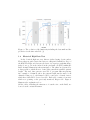
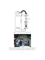
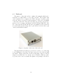
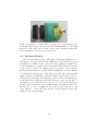
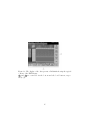
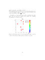
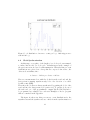
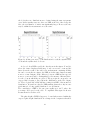
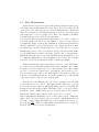
Electrical High Rate Test
Stephan Wiederkehr
Department of Physics, ETH Zürich
July 29, 2014
1
Contents
1 Introduction
1.1 LHC and CMS . . . . . .
1.2 Pixel Detector . . . . . . .
1.3 Luminosity . . . . . . . .
1.4 Electrical High Rate Test
.
.
.
.
.
.
.
.
.
.
.
.
.
.
.
.
.
.
.
.
.
.
.
.
.
.
.
.
.
.
.
.
.
.
.
.
.
.
.
.
.
.
.
.
.
.
.
.
.
.
.
.
.
.
.
.
.
.
.
.
.
.
.
.
.
.
.
.
.
.
.
.
.
.
.
.
.
.
.
.
2 Testing Procedure
8
3 Experimental Setup
3.1 Testboard . . . . . . . . . . . . .
3.2 Excitation Harness . . . . . . . .
3.3 DG2020A Data Generator . . . .
3.4 Rate Estimate and Measurement
4 Results
4.1 Early Results/Proof of
4.2 Clock Synchronisation
4.3 Pulse Height . . . . .
4.4 Pulse Length . . . . .
4.5 Rate Measurements . .
4.6 Desynchronisation . .
4.7 Chip Efficiency . . . .
3
3
3
4
6
Concept
. . . . .
. . . . .
. . . . .
. . . . .
. . . . .
. . . . .
.
.
.
.
.
.
.
.
.
.
.
.
.
.
.
.
.
.
.
.
.
.
.
.
.
.
.
.
.
.
.
.
.
.
.
.
.
.
.
.
.
.
.
.
.
.
.
.
.
.
.
.
.
.
.
.
.
.
.
.
.
.
.
.
.
.
.
.
.
.
.
.
.
.
.
.
.
.
.
.
.
.
.
.
.
.
.
.
.
.
.
.
.
.
.
.
.
.
.
.
.
.
.
.
.
.
.
.
.
.
.
.
.
.
.
.
.
.
.
.
.
.
.
.
.
.
.
.
.
.
.
.
.
.
.
.
.
.
.
.
.
.
.
.
.
.
.
.
.
.
.
.
.
.
.
.
.
.
.
.
.
.
.
.
.
.
.
.
.
.
.
.
.
.
.
.
8
11
12
13
17
.
.
.
.
.
.
.
19
19
21
25
27
31
33
37
5 Conclusion
43
6 Possible Further Studies
44
7 Acknowledgments
45
8 Appendix
47
2
1
Introduction
1.1
LHC and CMS
The Large Hadron Collider (LHC) is the latest and most powerful accelerator added to the European Organization for Nuclear Research (CERN Conseil Europen pour la Recherche Nuclaire). It consists of a 27 km long
ring in which 2 beam pipes carry the particles. The particles are forced into
a circular path by a magnetic field provided by superconducting electromagnets. There are several accelerating structures along the ring to boost the
particle energy. The beams travel opposite to each other and cross in specific areas where detectors are stationed to observe the collision of particles.
One of the four experiments located at the LHC, the compact muon
solenoid (CMS) has been designed to search for the Higgs boson and for
signs of Supersymmetry alongside the ATLAS experiment. To meet all the
requirements of such a task, the CMS detector consists of the following
elements, listing from centre:
• a tracking system, including:
– pixel detector
– silicon strip detector
• calorimeters, measuring the particles energy:
– electromagnetic calorimeter (ECAL)
– hadronic calorimeter (HCAL)
• solenoid
• muon chamber detectors
The solenoid, which is 7 meters in diameter and 13 meters long, provides
the experiment with a magnetic field of 3.8 Tesla.
Since the silicon strip detector cannot cope with the design luminosity close
to the beam, the innermost detector is made of silicon pixels which can
provide three dimensional information of each charged particle.
1.2
Pixel Detector
The CMS pixel detector is designed to measure precise hit information,
withstand radiation damage for multiple years of operation and using as
3
little material as possible to minimise multiple scattering of the particles.
The barrel part, consisting of three layers and two forward discs are arranged
such as to enclose the bunch crossings as good as possible. The described
layout of the detector is shown in figure 1. During the winter break in
2016/2017, the pixel detector will be replaced with an 4-layer barrel, 3-disk
endcap system. The fourth layer, added at a radius of 16 cm, will increase
the tracking precision and also serve as backup in case the first layer of the
strip detector degrades faster than expected. The layers are positioned at
the radii 30 mm, 68 mm, 109 mm and 160 mm, while the length of the barrel
extends to 548.8 mm. The support tube, carrying the pixel modules will also
be redesigned to avoid a large increase in material due to the added layer
and endcap discs. The detector is built in a modular concept. A module
consists normally of 16 readout chips (ROCs). A single ROC has 80 x 52
pixel channels, each of the dimension of 100 µm x 150 µm, yielding a total
of 78.8 million channels for the whole barrel part of the detector. To ease
the installation of the current detector around the beam pipe, it is built in
two halves motivating the construction of half modules.
Figure 1: Layout of the pixel detector before the upgrade. The three barrel
layers drawn in black and the four forward discs in purple. [2]
1.3
Luminosity
The LHC was designed to operate at a luminosity of 1 · 1034 cm12 ·s while
the particle bunches where set to collide every 25 ns. However, when it
4
started in 2009, the spacing between bunch crossings was 50 ns long. Increasing the centre of mass energy led to a peak luminosity of about 7 · 1033 cm12 ·s
in 2012. If the LHC can keep its level of performance, the luminosity will
be further increased along with the centre of mass energy, which is planned
to reach 14 TeV. As a next step, the spacing between bunch crossings will
be reduced to 25 ns after the first long shutdown (LS1). The development
of the luminosity in the past and the predictions for the future can be seen
in figure 2. With an increasing luminosity, even going beyond the initial
design luminosity, also the pixel detector is confronted with an increasing
rate of particle collisions. To cope with the increased requirements, a new
chip was designed and is presently under development. It will be installed
in the layers 2,3 and 4.
Therefore, in addition to the desire to reproduce hits in a common laboratory similar to those produced in the LHC, also the rate of those hits
experiences an increasing importance. Already existing methods to generate high hit rates are the beam test and the X-ray setup. The former can
emulate the situation encountered in the LHC very well, but it is a large
installation itself, where the latter can be used in a common laboratory, yet
it does only induce hits in single pixels instead of inducing hits in clusters,
as it happens in the LHC.
The electrical high rate test was developed as a small setup, suitable for
laboratories, which can induce clusters of pixel hits. It is the latest method
to induce pixel hits at a high rate for testing purposes.[1]
5
Figure 2: The evolution of the luminosity including the data until and the
prediction for the time after LS1. [3]
1.4
Electrical High Rate Test
In the electrical high rate test, hits are induced using electric pulses.
These pulses are guided via isolated wires to a Kapton foil which lies on top of
the ROC. The Kapton foil acts as a dielectric of a capacitor, such that charge
induced on top of it is also induced in the pixel unit cell (PUC) within the
ROC. A simple illustration is shown in figure 3. The pulses are generated by
a data generator, which allows to define pulse patterns in a tunable pattern
length. The used data generator was able to program different patterns
into a number of channels, where the pattern length was the same for all
channels. Using a pod, each channel could be connected to a bunch of wires,
which henceforth will be denoted as cable. Each cable consists of ten wires
which were pointing on the previously mentioned Kapton foil. Figure 4
illustrates the explanation above.
All the cables, including the structure to focus the wire on the ROC, are
denoted as the excitation harness.
6
Figure 3: A schematic
drawing of the basic
principle. Isolated wires
pointing on a Kapton
foil lying on the ROC.
The Kapton foil acts as
a dielectric of a capacitor.
Figure 4: An schematic illustration of the setup, featuring the data generator, the cables, the wires and the ROC. A more detailed description of the
setup can be found in section 3.
7
2
Testing Procedure
The first prototype ready for enhanced measurements of the excitation
harness (cf. section 3), which is the pivotal component of the eletrical high
rate test, was built at the Paul Scherrer Institute (PSI) before it was brought
to the ETH to test it. The goal of this work was to obtain a testing routine
to do experiments which require a certain hit rate. Therefore, the first step
was to reproduce the basic results of the setup, first and foremost the ability
to induce hits in a ROC.
As a second step, mechanisms which influence the rate were identified and
investigated. Also the precise procedure and setup for a rate measurement
was a priori not clear and was developed. Rate estimates and the deviation
from the measurements were analysed, as it is important to provide a desired
rate for more advanced measurements.
Finally, the chip efficiency was being tested. The efficiency test analyses the
output of the ROC with respect to the input, which is given by the provided
rate, and determines the efficiency of the readout process. Such efficiency
tests were done before with other methods, e.g. with X-rays. Therefore,
the efficiency test was used as a first example making use of a previously
defined rate, and it was a good opportunity to compare the results with
already established data.
3
Experimental Setup
A picture of the whole setup is shown in figure 5. Also, a schematic is
shown in figure 6, where the connections to the particular power supplies
are not drawn. In the real setup, a so-called pinboard appears. Its task is to
connect cables coming from the pod to the cables of the excitation harness.
Hence, the pinboard defines which channel, being output by the pod, is
connected to which cable of the excitation harness. A picture taken of the
pinboard is shown in figure 7. Another difference between the picture of the
real setup and the schematic is the connection between the testboard and
the clock input of the data generator. The connection was added after taking
the picture and enables the synchronisation of the internal clocks. However,
the connection alone does not suffice to synchronise the internal clocks. A
description of how the synchronisation can be achieved is given in the section
3.3. Independently of the synchronisation, unless mentioned otherwise, the
clock of the data generator was running with 40 MHz, as was the clock of
the testboard. Therefore, the data generator could be programmed in units
8
of 25 ns. Unless mentioned otherwise, the minimal pulse length of one clock
cycle ( = 25 ns) was used to induce hits.
The testboard was, in the end, running with the firmware 2.18. Primarily
USB problems, which seemed to be linked to the operating system (Ubuntu),
led to installing this version of the firmware.
Figure 5: A picture of the whole setup, taken before the first measurements.
The connection for the synchronisation of the clock (cf. figure 6) was added
later.
9
Figure 6: A schematic of the experimental setup.
Figure 7: A picture of the pinboard which connects the pod output cables
to the cables of the excitation harness. The blue jumpers show possible connections, where the black jumpers suppress a crosstalk between the cables.
10
3.1
Testboard
The purpose of the testboard is to emulate all commands which can be
addressed to a single ROC or even a whole module. The acquired data
can be transferred to a computer via a USB connection. A picture of the
testboard, taken of its front, is shown in figure 8. There are four LEMO
connections on the front of the testboard, where two are fixed connections to
put in a clock or a trigger, and thus are labelled CLK and TRG. The other
two connections, labelled D1 and D2 can be programmed. Both connections
were used in the presented setup. One to put out the clock, the other to put
out the synchronisation signal.
Figure 8: A picture of the front of the testboard.
The single ROC used in this project was wire bonded to a so-called chip
board. Furthermore, the chip board was connected to the testboard with
an adapter. Figure 9 shows the described setup fully connected. On the
adapter, several labelled dot contacts can be identified. With an oscilloscope they can be used to measure the signals corresponding to the labels.
11
Figure 9: A picture of a single ROC on a chip board. An adapter is connecting the chip board to the testboard. The small installation on the right
hand side of the chip board is a basic version of the excitation harness and
was not installed for the project presented here.
3.2
Excitation Harness
The excitation harness is the central part of the setup guiding the electric pulses to the ROC and inducing signals in it. Following the previous
description, it consists of wires, grouped in cables, which are gathered in a
block (of plastic) to focus the wires on the ROC. The Kapton foil is fixed
to the bottom of the block. Figure 10 shows a picture of the excitation
harness already attached to a ROC. When attaching the excitation harness
to a ROC, the block is screwed on the chip board. The chip board is a small
printed circuit board (PCB) to which the ROC is wire-bonded. The two
drilled holes in the chip board define the position of the block with respect
to the ROC. A few splitters of the ROC waver were placed at the sides of
the ROC, before screwing the block on top of it, to protect the ROC from
pressure. The actual effect of those splitters was not investigated and is not
known. As one can see in figure 10, the cables are all connected to each
other. This is to connect all of the cables to ground, which is done by the
black cable shown in the figure.
12
Figure 10: A picture of the excitation harness attached to a ROC. The black
cable is the connection to ground.
3.3
DG2020A Data Generator
In this section a more detailed description the the data generator will be
given along with a few examples of how to use it. The goal is to help using
the presented setup, not to substitute the manual. It is highly recommended
to read the latter. The data generator in question was the model DG2020A
from Tektronix (Sony), where the pod model was P3410. The figures 11
and 12 show schematics of the front and rear panel of the data generator,
respectively. The figure 13 shows a picture of its display while in the EDIT
menu.
13
Figure 11: The front panel of the data generator DG2020A. [4]
Figure 12: The rear panel of the data generator DG2020A. [4]
14
Figure 13: The display of the data generator DG2020A showing the typical
content of the EDIT menu.
1 and 2 are controlled via the bottom and side bezel buttons, respectively. [4]
15
Connecting the DG2020A:
To use the data generator only the power connector needs to be connected
while the principal power switch must be switched on (cf. figure 12). To
output channels, a pod needs to be connected to one of the three pattern
data output connectors. The clock synchronisation can be achieved by connecting the testboard to the clock in connection. Note that the testboard
supports LEMO connections, while the clock in supports SMB connections.
Once a pod is connected, the channels of the data generator must be assigned to the pod outputs. The assignment is explained below. To navigate
through the menus described in the following, use the bottom and side bezel
buttons (cf. figure 11).
Setting the internal clock:
Enter the SETUP menu and open the OSCILLATOR menu. First the source
can be chosen. To synchronise the clock with the testboard clock, choose
EXT. To enable the generation of an internal clock, select INT. If an internal clock is used the PLL should be turned ON. If an external clock is used
the PLL must be turned OFF. Using an internal clock, its frequency can be
chosen pressing INT FREQUENCY. If an external clock is used, the EXT
FREQUENCY influences the displayed frequency, e.g. in the EDIT menu,
and should therefore be chosen as close as possibly to the actual external
frequency.
Editing the channels:
To edit the channels enter the EDIT menu. Subsequent, a display will appear similar to figure 13. The leftmost entry in each row displays the name of
the channel. The pattern length can be edited pressing SETTINGS → SET
MEMORY SIZE. The memory size is then entered in units corresponding
to the pattern unit length, which is 25 ns if the internal clock has been set
to match the clock of the testboard. To edit a pattern, select EXECUTE
ACTION → SET DATA TO HIGH or SET DATA TO LOW. Select the
channel using the arrow buttons. Then use the general purpose knob or the
arrow buttons to select the bit and press the EXECUTE button to edit the
bit. To edit multiple bits at once in the same channel, press the CURSOR
button, change the cursor size with the general purpose knob and press the
CURSOR button again.
Editing the run mode:
To choose the run mode, select the SETUP menu and press RUN MODE.
Now, a variety of run modes can be selected, where the most important ones
16
are the REPEAT and the SINGLE mode. To send the patterns repeatedly,
select REPEAT. If the trigger (which the testboard sends to the ROC) shall
be synchronised with the pattern, select SINGLE. The SINGLE mode will
send the pattern once (!) each time the data generator receives a trigger
(corresponding to the synchronisation signal output by the testboard) in the
trigger input (cf. figure 11).
Assigning channels to the pod:
Press the SETUP button and select the POD ASSIGN menu. This opens
a new window in which the general purpose knob can be used to select the
internal channels (e.g. DATA01). The arrow buttons are used to select the
output channel of the pod (e.g. A-01).
Press the START/STOP button to start or stop the output of the pulse
patterns.
3.4
Rate Estimate and Measurement
It is very important, for the understanding but also to program the data
generator accordingly, to be able to estimate the hit rate. In principle, the
rate corresponds to #hits
time . Since for all rate measurements the data generator
sent the programmed pulse pattern repeatedly and without a delay between
two patterns, the relevant time is the pattern length. Within the pattern
length, the amount of hits is given by the amount of hits generated by each
pulse multiplied by the amount of pulses. This is summarised in equation
1, where Np is the amount of pulses, Nh is the number of hits per pulse, M
is the pattern length given in µs and AROC is the area of the ROC. With a
desired rate given, the formula can be applied to estimate the pattern length
and the amount of pulses to place in it.
rate [
Np · Nh
M Hz
1
]=
·
2
cm
M
AROC
(1)
To measure the rate, a sequence consisting of a CAL (calibrate), a TRG
(trigger), a TOK (token) and a delay was sent to the ROC.
The CAL signal injects charge in a pixel to emulate a hit. Unless the pixel is
armed, though, the charge is not being switched through, such that it does
not influence the pixel. The TRG signal indicates the data to be readout,
before the TOK signal starts the readout process. The data readout with
one trigger is sometimes also called an event. In general, an event may or
may not contain hits. In the following, events containing hits are labelled
17
non-zero events.
The delay consisted of a fixed part and a random contribution. The fix delay
was set to 10 µs to provide enough time for the chip to read the data out.
The random part varied between 0 and 50 µs.
The sequence can be sent in two ways, either via the Pg Single command
or via the Pg Loop command.
The Pg Loop command sends a defined sequence and a defined delay repeatedly. The user can define the start, the time during the command shall run
and the stop. The amount of sent triggers can be calculated using the time
of one loop (sequence + delay) and the duration of the command. Since the
calculation may differ from the actual amount of triggers sent, the Pg Single
command was used.
The Pg Single command sends the afore defined sequence one. Hence, to
send e.g. 1000 triggers, the Pg Single command must be executed 1000
times.
It was found, that sending those single shots led to an additional, not
constant delay.
Therefore, the total delay amounted to about 275 µs on average, corresponding to a trigger rate of roughly 3.6 kHz. The triggers were sent to the
testboard using a single command. However, in the test program, the total
amount of triggers was split up using a for loop as shown in the pseudo code
below. In the following, the amount of loops. inside such a for loop, will be
referred to just as loops.
f or (loops)
send(x sequences (each sent as P g Single))
The random delay and the loops were applied to randomise the readout. Ideally, the hits would occur randomly. However, since they have to
be programmed and therefore are not random, the readout was randomised
instead.
The program measuring the rate (cf. the appendix) essentially executed
the for loop shown above, collected the data and calculated the rate. The
data contained the amount of events corresponding to the number of triggers
sent.
Each event comprised the amount of hits, including the information about
18
the their pulse height (not calibrated) and their pixel address.
The rate was calculated by dividing the number of hits and by the total
number of triggers (loops · #triggers per loop) according to equation 2,
where Nhits is the amount of hits, Ntrg is the amount of triggers, τ (= 25
ns) is the clock cycle length, AROC is the area of the ROC and C (= 40)
M Hz
converts the rate from 40cm
into McmHz
2
2 .
rate [
4
1
M Hz
Nhits
C
·
]=
·
2
cm
Ntrg
τ
AROC
(2)
Results
4.1
Early Results/Proof of Concept
The result of an early rate measurement is shown in figure 14. The
figure shows a map of the ROC where the amount of hits is plotted as a
function of position. Indeed, each wire induces a cluster of roughly 10 pixel
hits. However, only eight clusters can be seen, even though ten clusters were
expected after connecting one cable.
Unfortunately, the observation of less than ten wires was the generic case.
The reasons were found to be one of the following:
• The wires did not point on the ROC.
• The wires were not close enough to the Kapton foil, let alone touching
it. This is discussed further in the section 6.
• The wires were broken or badly soldered.
Figure 15 shows a distribution of non-zero events per loop, where an
event describes a readout clock cycle. As the readout process is assumed
to be random, a Poisson distribution was expected. Furthermore, since the
depicted mean corresponds well to the maximum of the distribution, the
mean is equivalent to the probability to encounter a non-zero event in a
loop. The probability can be read off dividing the mean by the number of
triggers per loop, in this case 1000. This probability can be compared to the
probability given by the data generator. The latter is simply the amount of
pulses divided by the pattern length, assuming a pulse induces hits in only
one clock cycle.
As an example:
The measurement shown in figure 15 was done with 1000 triggers per loop,
19
which corresponds to a probability of 1.724 %.
The measurement was done with only one cable. The pulse pattern was 58
clock cycles long and contained one pulse of one clock cycle. Therefore, the
1
expected probability is equal to 58
≈ 1.724 %.
Generally, a good agreement between those probabilities was found.
Hence, the clock cycles were, roughly, readout equally often, confirming
the assumption of a random readout.
Figure 14: The typical outcome of a rate measurement. Only one cable is
connected. The amount of hits is plotted as a function of position.
20
Figure 15: A distribution of non-zero events per loop. 1000 triggers were
sent in 100 loop.
4.2
Clock Synchronisation
At this stage, every pulse, of the length of one clock cycle, was assumed
to induce hits in only one clock cycle. Calculations as in the example of
the previous section are based on this assumption. When the hits per event
distributions were plotted, two clear peaks were expected. One at zero, the
other at about 80 hits, since:
8 clusters · 10 hits per cluster = 80 hits
However, measurements done with the clocks from the testboard and the
data generator running asynchronously, led to the detection of so-called
low-hit-events (LHE).
Thereafter, the clocks were always synchronised by putting the clock of the
testboard into the data generator (cf. sention 3.3). To put the clock out of
the testboard, one of the programmable outputs (labelled D1/D2) had to
be programmed accordingly before each test. Examples of how to program
this are contained in the appendix.
The figure 16 shows two hits per non-zero event distributions for the
asynchronous and the synchronous case. Aside from the synchronisation of
21
the clock, these two distributions were obtained using the same test parameters. In the asynchronous case, there are LHE on the left of the clear peak.
Also, the total number of entries was significantly larger. However, the rate
stayed, within the measurement error, the same.
Figure 16: A hits per non-zero event distribution for each, the asynchronised
clock and the synchronised clock case.
A closer look at LHE revealed the data shown in the figures 17 and 18,
where the former displays a ROC map of only one non-zero event and the
latter shows the result of the whole rate measurement containing all hits.
As can be seen in the two figures, the LHE are in the same clusters as usual
non-zero events. In figure 18 the difference between a LHE and an expected
non-zero event can clearly be distinguished by the amount of hits and therefore the colour in which they are plotted. The green pixels correspond to an
expected hit belonging to the peak in the distribution on the left of figure
16. The red pixels saw additional hits coming from LHE of the mentioned
distribution. It is unclear, why the LHE manifest themselves only in some
pixels instead of being equally distributed over all clusters.
The contribution of LHE to the rate was roughly up to 40 %, where the
percentage did depend on the cable. To emphasise this, figure 19 shows a
measurement for another cable.
The pulse height of LHE did appear to be randomly scattered within the
expected pulse height distribution as a change in the comparator threshold
22
did not extinguish the LHE. Neither did the relative contribution to the rate
change significantly. It was not investigated whether the pulse height of a
particular pixel changes when the pixel is part of an LHE w.r.t. when it is
part of an usual hit.
It is being assumed that running the clock asynchronously “splits” some
pulses into two clock cycles, where each contains a fraction of the total
amount of hits. This would explain the increased number of non-zero events,
as well as the occasionally reduced amount of hits within such an event. The
LHE were not investigated more intensely and remain not fully understood,
though.
The probability of a non-zero event, as discussed in the previous subsection,
was significantly influenced by LHEs, and therefore impaired a comparison
with estimates. Since such comparisons were exceedingly important at this
stage of the experiment, the clocks were synchronised for all following test,
unless mentioned otherwise.
Figure 17: A ROC map displaying a single LHE. The amount of hits is
plotted as a function of position
23
Figure 18: A ROC map, where the amount of hits is plotted as a function
of position. The red pixels indicate LHE, while the green pixels indicate an
expected hit corresponding to the peak in figure 16.
Figure 19: A hits per non-zero event distribution. The difference to the data
shown in figure 16 is the amount of pulses used and the connected cable.
24
4.3
Pulse Height
As whole clusters of hits are induced, it was a priori not clear how the
pulse height would be distributed. Beforehand, a pulse height calibration
was done to assign an amount of charge to the digital value delivered by the
pixel.
Figure 20 shows a ROC map, where the pulse height was plotted as a function of position. From the figure it becomes clear that the pulse height is
not uniform over a cluster which leads to the broad pulse height distribution
shown in figure 21. As a consequence, the rate can be tuned gradually by
varying the comparator threshold. Figure 22 shows a plot, where the rate
is plotted as a function of the comparator threshold. Indeed, the increase
in the rate is gradual until the threshold is on the level of the noise, which
occurs at a VthrComp value of about 135. VthrComp is a digital to analogue
converter (DAC) which determines the height of the comparator threshold.
Figure 20: A ROC map. The pulse height is plotted as a function of position.
25
Figure 21: A typical distribution of the pulse height per hit.
Figure 22: The rate is depicted as a function of the comparator threshold.
26
4.4
Pulse Length
While the early measurements where done with a haphazardly chosen
pulse length, the necessity of a proper investigation of its influence became
pressing subsequently.
It was impossible, though, to analyse particular clock cycles with a random
trigger. Therefore, the trigger and the pulse had to be synchronised. The
synchronisation was achieved by adding a synchronising signal to the sequence, as depicted schematically in figure 26. One of the programmable
outputs of the testboard was programmed to put out the synchronisation
signal as it was done with the clock (cf. section 4.2). This particular signal output was then connected to the trigger input of the data generator
which was programmed as to send the sequence only once after receiving
the synchronisation signal from the testboard (cf. the paragraph about the
run mode in section 3.3).
Since the synchronisation signal was synchronous w.r.t. to the (testboard)
trigger and w.r.t. the pulse of the data generator, the trigger was synchronous w.r.t the pulse.
As illustrated in the schematic, the WBC value determines which clock cycle
is read out while the tct value determines the distance between the calibrate
signal and the trigger signal. In the following measurements the tct value,
instead of the WBC value, was varied to scan through the region of the
pulse. The usage of the tct value or the WBC value is equivalent, and the
unit of both values is given in clock cycles.
The figures 23, 24 and 25 show the amount of hits plotted as a function
of the tct value for different pulse lengths. As mentioned before (cf. section
3), the unit length of the pulse length is given in clock cycles as well.
In figure 23, it is clear to see, that there are only hits in one clock cycle
when using the smallest possible pulse length. On the other hand, figure
25 indicates clearly, that the rising edge as well as the falling edge cause
hits. Keeping this in mind, the contribution of the rising edge as well as the
falling edge can also be identified in figure 24. However, there are also hits
in between the two edges. The contribution of hits in between the edges was
found to be largest at pulse lengths of about 5-7 clock cycles. At a pulse
length of about 25 clock cycles, this contribution is very small, yet, further
increasing the pulse length does not necessarily extinguish this contribution. It can be avoided, though, by increasing the comparator threshold.
In the same way the whole contribution from the rising edge or the total
contribution from both edges can be erased. All performed pulse length
27
measurements are shown in the appendix.
In the schematic in figure 26 also the pulse, as it is assumed to behave inside
the ROC, is drawn along with the comparator threshold voltage. The chip
is designed such that it reacts only on falling edges. Therefore, whenever a
falling edge crosses the level of VthrComp , a hit is induced in a pixel. Thus,
in theory, only the falling edge of the pulse was expected to induce hits.
The contribution of the rising edge, as well as the contributions in between
the edges are attributed to the post flank oscillations. It is, however, not
understood how these oscillations cause what is depicted in figure 24 and
25.
For instance in figure 25, and considering the schematic, it is unclear how in
the contribution of the rising edge (pulse) even the second falling edge (post
flank osc.) seems to induce hits, while in the contribution of the falling edge
(pulse) only the first falling edge (post flank osc.) induces hits.
Figure 23: The amount of hits as a function of tct. The unit length of a
pulse is 25 ns.
28
Figure 24: The amount of hits as a function of tct. The unit length of a
pulse is 25 ns.
Figure 25: The amount of hits as a function of tct. The unit length of a
pulse is 25 ns.
29
Figure 26: A schematic of the signal synchronisation. Additionally, the post
flank oscillations are drawn.
30
4.5
Rate Measurements
As the hit rate is generated by the pulse pattern, which was sent repeatedly during rate measurements, the exact rate is given by reading out all
clock cycles of the pulse pattern once and averaging the hits contained in
them. For a random readout this means that every clock cycle of the pulse
pattern should be read out equally often. Hence, the amount of statistics
determines the precision of the rate measurement.
It was found, that at least 100,000 triggers have to be sent to achieve a
reasonably small error. Moreover, the influence of the loops was found to
be significant. Figure 27 shows the distribution of 600 rate measurements,
all done with 100 loops and 1000 triggers each. Figure 28 shows a similar distribution, but the measurements were done with only one loop and
100,000 triggers in it. The total amount of triggers in the measurements
of both distributions is therefore the same. However, the root mean square
(RMS) shown in the inset box in each distribution indicates that the loops
do contribute significantly to the randomness of the readout. For comparison, table 1 shows the mean and the RMS for different settings.
Using measurements, such as the hits per non-zero event distribution,
to get more precise information than merely vague estimates, the formula
in equation 1 yielded values very close to the measured rate. The formula
proved to be the most accurate way to program the data generator to provide a certain hit rate. Due to the finite width of the mentioned hits per
non-zero event distribution and the error in the measured rate, a fine tuning
of the data generator was necessary in most cases.
It should be noted that the rate can only be measured correctly with
a pixel efficiency close to 100 %. Increasing the rate will lead to a strong
decrease in the pixel efficiency which will finally reach 0 % such that the
measurable rate has an upper limit. This limit could be overcome by inducing hits in double columns which were previously not hit by any clusters.
This means, that the upper limit depends on the choice of cables.
Hence, this limitation is attributed to an overflow in the double column data
buffer. Since each cable induces up to ten clusters, which might all lie in
the same double column, this limit can occur at relatively low rates, e.g.
at about 100 McmHz
2 . Therefore, this limitation should always be considered
when choosing cables for a rate measurement.
31
Figure 27: A distribution of 600 rate measurements, all done with 100 loops
and 1000 triggers each.
Figure 28: A distribution of 500 rate measurements, all done with 1 loop
and 100,000 triggers each.
Table 1: The mean and RMS of rate distributions for different settings.
Measurements
loops
triggers per loop
mean rate [ McmHz
2 ]
RMS [ McmHz
2 ]
100
100
100
100
100
10
100
10
100
100
10
10
100
100
1000
124.8
141.48
128.91
115.74
136.47
83.56
33.13
45.83
9.14
4.07
32
4.6
Desynchronisation
There were reports of an issue when reading out data. Specifically, it
seemed that data belonging to one trigger were readout with the next or the
previous one. This shift, which is called desynchronisation, could also be
investigated with the current setup. To do so, a new sequence (cf. section
3.4) was defined consisting of the following signals.
CAL + TRG + TOK + delay + TRG + TOK + delay
The delay was 510 clock cycles long, the time between CAL and TRG
(tct) was 106 clock cycles long and the time between TRG and TOK (ttk)
was 32 clock cycles long.
A particular pixel was armed, such that the voltage defined by VCal was
switched through and read out by the first trigger, only. At the same time
the data generator was providing pulses at an afore determined rate. The
address of the armed pixel was chosen not to lie within a cluster, such that
the test could search for a particular pixel address to identify the VCal .
As the readout was random, both triggers may or may not contain hits due
to the electric pulses. The CAL signal was, however, a fix part of the sequence such that the VCal was expected in every even trigger, as the counting
started at zero.
The first test did break when encountering the first error and produced four
ROC maps in total, each plotting the amount of hits as a function of position. An error was produced when either the VCal was found in an odd
trigger, or no VCal was found in an even trigger.
The first map contains all hits gathered during the test. The map labelled
“error” contains the data belonging to the trigger which produced the first
error, while the maps labelled “previous” and “after first error” contain the
data belonging to the trigger preceding or following the error, respectively.
Figure 29 shows the outcome of two measurements. In the measurement on
the left the VCal simply vanished, while in the measurement on the right the
VCal was shifted to the next (odd) trigger.
The error was typically found after 300, 000 ± 50, 000 triggers and did
not depend on the rate, as it also occurred with the data generator turned
off. As a first step, the data flow on the testboard was changed. This was
done by increasing the parameter buffsize from its default value (2097152) to
5,000,000 and additionally increasing the parameter blocksize successively,
starting at its default value 8192.
As a result, increasing those parameters did also increase the trigger num33
ber at which the first error occurred. At the value blocksize = 1, 000, 000 no
error was found during ten measurements, each sending 2,000,000 triggers.
The figures 30 and 31 show essentially the same test, though it was modified not to stop at the first error, but to plot all the events in a certain range
around it. The hits caused by the electric pulses are clearly visible as those
events contain more than the one hit due to the VCal . The entries plotted
in green correspond to events which passed the error test, while the entries
plotted in read produced errors according to the definition above. To see
errors at all, the blocksize was set to its default value again.
Figure 31 is particularly interesting, because the VCal returned to the even
events after a period in which it was found in the odd events. It is not clear
whether the VCal shifted twice in the same direction, or if it shifted back
and, therefore, restored the original synchronisation.
In summary, the desynchronisation was not found to depend on the hit
rate. Only the blocksize and buffsize values were found to influence the appearance of the effect. The desynchronisation was not further investigated,
because it did not appear with the blocksize and buffsize values mentioned
above.
34
Figure 29: Two desynchronisation measurements. The amount of hits is
plotted as a function of position.
Left: The VCal expected in an even trigger vanished. The precedent and
following trigger contain no VCal , as expected.
Right: The VCal expected in an even trigger was shifted into the following,
odd trigger.
35
Figure 30: A desynchronisation measurement. The amount of hits is plotted
as a function of the event.
Figure 31: A desynchronisation measurement. The amount of hits is plotted
as a function of the event.
36
4.7
Chip Efficiency
After the hit rate was well understood and a procedure was found to
produce a desired rate, the next step was to use the acquired knowledge to
perform a more advanced test. The more advanced test was in fact an early
chip efficiency test, for which the setup was built.
The efficiency of a pixel was tested by switching through a VCal and
reading it out again, while the chip had to deal with the hits induced by
the data generator. Therefore, the efficiency of a pixel corresponds to the
readout VCal s divided by the total amount of VCal s sent. The latter is
equivalent to the total number of triggers sent, since the sequence sent to
the chip was the same as for a rate measurement (cf. 3.4).
Therefore, the efficiency corresponds to the following formula, where NCal
is the number of readout VCal s and Ntrg is the number of triggers.
pixel ef f iciency =
NCal
Ntrg
All pixels of the ROC could not be armed at once, due to memory
limitations, but it was armed row by row. The full procedure of a test was
the following:
• A single reset signal was sent.
• A whole row of pixels was armed and another single reset signal was
sent.
• The sequences were sent to the ROC. A total of 100,000 triggers were
sent in 100 loops and 1000 triggers each.
• The readout VCal s were plotted in a ROC map as a function of position.
• The whole ROC was unarmed and the procedure started anew. After
the last row the test ended.
According to the procedure, the outcome of such a test was a ROC map
where the pixel efficiency was plotted as a function of position. Figure 32
shows a so-called efficiency map at a hit rate of 300 McmHz
2 . As one can see
by the clusters of lesser efficiency, these tests were performed using five cables to distribute the clusters over the whole ROC. The analysis is shown
in figure 33. One can clearly see a peak at 100 %. In addition, on the left
a separate region can be distinguished. The pixels in this region belong to
37
the particularly affected double column in figure 32. The mean efficiency
of such a test was then extracted and plotted against the rate, as shown in
figure 34.
The error in the rate was taken from the rate distribution in figure 27. The
error in the efficiency was taken from the distribution in figure 35, where
the distribution of 30 efficiency test is shown. The efficiency tests for this
distribution were, however, done only over the rows 40 - 60 to decrease measurement duration.
In figure 34, the efficiency does not change, within the error, as the rate
increases from 300 to 350 McmHz
2 . This is attributed to the method used to
M Hz
increase the rate to 350 cm2 .
In section 4.5, an upper limit to the measurable rate is mentioned. This
limit was reached soon after 300 McmHz
2 . To increase the rate anyway, two
of the five cables were chosen which had a negligible overlap in terms of
affected double columns. This means that the clusters of those two cables
did lie in different double columns such as not
to increase the data in the double column data
buffers. To increase the rate, an additional
pulse was sent to one of those cables at the
same time when a pulse was sent through the
other cable. This situation is schematically
shown in the schematic on the right.
This method allowed the measurement of a higher rate. On the other hand,
a further drop in the efficiency of the strongly affected double column, shown
in figure 32, was clearly avoided as the additional hits were all in other double columns.
Figure 36 shows the efficiency and the local rate as a function of the
double column in the left column, and the efficiency as a function of the
local rate in the right column. The plots contain the data for the rates 253
M Hz
M Hz
, 300 McmHz
2 and 353 cm2 , as these were the least expected results. The
cm2
remaining data can be found in the appendix.
The local rate was calculated as in equation 3, were Nhits is the number of
hits, Ntrg is the number of triggers, τ is the clock cycle length, ADC is the
area of the double column and C converts the rate to MHz.
local rate [
M Hz
Nhits
C
]=
·
2
cm
Ntrg τ · ADC
38
(3)
The efficiency was expected to decline steadily as a function of the local rate. Yet, the difference in efficiency between the double columns at a
relatively low local rate is too large to see any tendency. The only clearly
visible decline was observed if the local rate exceeds 16 McmHz
per double
2
M Hz
column at a total rate of 300 cm2 . There, the efficiency dropped below
40 %. Including the data for 353 McmHz
2 , the reason for this jump becomes
unclear.
Contrariwise, it is not understood why, at 353 McmHz
2 , there are two double
columns which have an efficiency over 90 % at a local rate of over 16 McmHz
2 .
Especially, since the the local rate did not decrease, compared to the measurement done at a total rate of 353 McmHz
2 .
Figure 32: An efficiency map at 300
plotted as a function of position.
M Hz
.
cm2
39
The amount of readout VCal s is
Figure 33: The analysis of the pixel efficiency map at 300
of pixels as a function of their efficiency.
M Hz
.
cm2
The number
Figure 34: The mean efficiency as a function of the rate.
40
Figure 35: A distribution of 30 efficiency measurements. Each measurement
was done for the rows 40-60.
41
Figure 36: Left: The efficiency (x) and the local rate (o) (cf. eq. 3) as a
function of the double column.
Right: The efficiency as a function of the local rate.
The plots contain the data, starting on top, from the efficiency maps for 253
M Hz
M Hz
, 300 McmHz
2 and 353 cm2 .
cm2
42
5
Conclusion
The electrical high rate test produces, indeed, clusters of pixel hits at
a tunable rate. Moreover, the rate agrees well with estimates which allow
to predict the measured rate and program the data generator accordingly.
However, high rates can only be measured with a specific choice of cables.
The accuracy of rate measurements depends on the amount of statistics,
as expected. Yet, the required amount of statistics depends on the randomness of the readout.
Using a total of 100,000 triggers yielded an error of about 2 McmHz
2 . The total
amount of triggers was split using a for loop. In future experiments, a more
sophisticated method to realise a random readout might help to decrease the
necessary amount of triggers.
Synchronising the internal clocks of the data generator and the testboard
proved to be important to control the amount of non-zero events and the
amount of hits within each. With the clocks being synchronised, the pulse
length does not matter when it comes to rate calculation, since the contributions of the edges and between are very reproducable and can be included
in the estimate.
However, for most measurements the pulse length of one clock cycle is the
easiest to handle as there are only hits in one clock cycle, per pulse.
Furthermore, the setup was successfully used to test the chip efficiency.
The mean efficiency per pixel was found to be over 98 % for rates below
150 McmHz
2 . Comparing the result shown in figure 34, with data obtained by
X-ray experiments, the efficiency is already relatively low even below 150
M Hz
. The reason for this difference is attributed to the different amount of
cm2
hits per non-zero event. While in this experiment, there are about 80 hits in
a non-zero event, there are only about 3 hits per non-zero event using X-rays
at the same rate. Similar is the situation for the affected double columns.
In this experiment, an affected double column contains usually about 5 hits,
while there is rarely more than one hit per double column using an X-ray
setup.
Therefore, in an affected double column the rate can easily reach 100 McmHz
2
or more.
To increase the comparability, the amount of wires per cable could be reduced to decrease the amount of hits caused by one pulse.
43
Looking at the rates in the double columns separately, the expected
decrease of the efficiency with increasing rate is merely hinted. It is unclear
why there is a fluctuation of the efficiency, even at relatively low rates, of
up to roughly 4 %.
6
Possible Further Studies
An issue encountered with the actual setup, was the mechanical sensitivity of the excitation harness. Connecting and disconnecting cables can
require a strength which is enough to pull a wire from the ROC. As all the
wires are tightly compressed, when focusing them on the ROC, the wire will
not return, once it has been pulled away.
This could be avoided by using e.g. a PCB as interconnection between the
excitation harness and the data generator. The PCB could be part of a fixed
structure, such that the user does hardly touch the excitation harness, once
the ROC has been attached.
Generally, the control over the cluster position should be increased. At
the same time, one could decrease the amount of wires per cable. Ideally,
the wires should be connected separately, such that the distinction of cables
and wires becomes redundant.
As a suggestion, one could place the wires on top of the Kapton foil in
a well defined pattern. Since the patter is known, this would enable the
determination of the cluster position.
44
7
Acknowledgments
I would like to thank Prof. Dr. Rainer Wallny for making this work
possible, and letting me be part of the very enjoyable and helpful atmosphere. Furthermore, I would like to thank Dr. Andrey Starodumov and
Dr. Wolfram Erdmann for their assistance and support during the project.
45
References
[1] The information used in the introduction was partially taken from the
CMS TECHNICAL DESIGN REPORT FOR THE PIXEL DETECTOR UPGRADE,
ISBN 978-92-9083-380-2
[2] D.Kotlinski, R.Baur, K.Gabathuler, R.Horisberger, R.Schnyder and
W.Erdmann, Readout of the CMS Pixel Detector.,
http://ph-collectif-lecc-workshops.web.cern.ch/ph-collectif-leccworkshops/LEB00 Book/tracker/kotlinski.pdf (online 20.08.2012)
[3] The original picture was taken from a presentation of Jorgen Beck
Hansen, “Physics at run 2”.
[4] The original pictures are taken from
User Manual, “DG2020A, P3410, & P3420”, Data Generator and Pods,
Sony/Tektronix Corporation, P.O. Box 5209, Tokyo Int’l, Tokyo 100-31
Japan,
Tektronix, Inc., P.O. Box 1000, Wilsonville, OR 97070-1000
46
8
Appendix
Figure 37, 38 and 39 show all pulse length scans (cf. section 4.4). Since
the data generator did run with the clock of the testboard, the unit length
of the pulse is given by 25 ns.
All efficiency maps and their analyses are summarised in figure 40, 41
and 42. The error in the rate is ≈ 2 McmHz
2 according to figure 27.
All important programs and root makros which where used can be found
on the provided CD ROM. A brief description is given in the following.
dceff1.C Takes an efficiency map (pa.py) as input and outputs the efficiency and local rate per double column as well as the efficiency as a
function of the rate for each double column.
double.py performs the desynchronisation test as shown in figure 29. The
function adc2() defines the sequence and is not given by default. It
can, though, easily be rewritten using the adc() function, given in the
file containing the testboard functions (DTB.py).
doubleC.py performs the desynchronisation test as shown in, e.g. figure
30. This test also makes use of the adc2() function.
eff.cxx takes an efficiency map as input provided by either pixelalive.py or
pa.py. In the former case, it produces three pixel efficiency plots. One
for all pixels, a second one for all affected double columns and a third
for all clusters. In case of a map, provided by the pa.py program, it
produces the efficiency for all pixels only, as for instance in figure 33.
efferror.C produces the plot shown in figure 35. The data is hardcoded.
effhisto1.C produces the plot shown in figure 34. The data is hardcoded.
functions.py provides a couple of functions to use the pulse height calibration data.
lhe.py produces 5 ROC maps containing single LHEs, as e.g. in figure 17.
map.py measures the rate and produces a ROC map, a hits per non-zero
event distribution, a non-zero event per loop distribution and a pulse
height distribution.
47
pa2.py performs an efficiency test and produces an efficiency map. It arms
each pixel separately (instead of a whole row) and was used for debugging.
pa-error.py performs numerous efficiency tests. It provided the data for
the efferror.C makro. In the beginning, a rate measurement is included
to avoid a reinitialisation of the ROC.
pa.py performs an efficiency test and produces an efficiency map. It performs a rate measurement in the beginning, to avoid a reinitialisation
of the ROC.
param.py contains the testing parameters used in map.py, pixelalive.py,
pa.py, pa2.py, lhe.py and rate-vs-thr.py
pixelalive.py performs an efficiency test and produces an efficiency map.
rate-to-histo.py takes a text file containing the output of map.py and
produces a rate distribution.
rate-vs-thr.py performs rate measurements while sweeping through an interval of VthrComp . It produces a plot as show in figure 22.
scan-tct.py performs a pulse length scan as shown in figure 23. The synchronising signal must be added to the sequence.
48
Figure 37: The amount of hits as a function of tct. The unit length of a
pulse is 25 ns.
49
Figure 38: The amount of hits as a function of tct. The unit length of a
pulse is 25 ns.
50
Figure 39: The amount of hits as a function of tct. The unit length of a
pulse is 25 ns.
51
Figure 40: Efficiency maps, where the pixel efficiency is shown as a function
of position. The rate is shown in the top left corner of each map.
52
Figure 41: Efficiency map and plots, where the pixel efficiency is shown as a function of position and the amount of pixels is shown as a function of their efficiency,
respectively. The rate is shown in the top right or top left corner of each plot or
map, respectively.
53
Figure 42: Pixel efficiency plots, where the amount of pixels is shown as a
function of their efficiency. The rate is shown in the top right corner of each
plot.
54
Figure 43: The efficiency (x) and the local rate (o) (cf. equation 3) as a
function of the double column. The total rate is shown in the top right
corner of each plot.
55
Figure 44: The efficiency as a function of the local rate (cf. equation 3) for
each double column. The total rate is shown in the top right corner of each
plot.
56