1
Freescale Semiconductor, Inc.
PREFACE
Freescale Semiconductor, Inc...
The complete documentation package for the MC68330 consists of the MC68330
Integrated CPU32 Processor User’s Manual (MC68330UM/AD) and the MC68330
Integrated CPU32 Processor Technical Summary (MC68330UM/D).
The MC68330 Integrated CPU32 Processor User’s Manual describes the programming,
capabilities, registers, and operation of the MC68330. The MC68330 Integrated CPU32
Processor Technical Summary provides a description of the MC68330 capabilities and
detailed electrical specifications.
This user’s manual is organized as follows:
Section
Section
Section
Section
Section
Section
Section
Section
Section
MOTOROLA
1
2
3
4
5
6
7
8
9
Device Overview
Signal Descriptions
Bus Operation
System Integration Module
CPU32
IEEE 1149.1 Test Access Port
Applications
Electrical Characteristics
Ordering Information and Mechanical Data
MC68330 USER’S MANUAL
For More Information On This Product,
Go to: www.freescale.com
Freescale Semiconductor, Inc.
TABLE OF CONTENTS
Paragraph
Number
Title
Page
Number
Freescale Semiconductor, Inc...
Section 1
Device Overview
1.1
1.2
1.2.1
1.2.2
1.2.3
1.2.4
Central Processor Unit .................................................................................... 1-2
System Integration Module.............................................................................1-2
System Configuration and Protection Submodule.....................................1-2
Clock Synthesizer.............................................................................................1-3
Chip Selects ......................................................................................................1-3
External Bus Interface......................................................................................1-3
Section 2
Signal Descriptions
2.1
2.2
2.2.1
2.2.2
2.3
2.4
2.5
2.6
2.7
2.7.1
2.7.2
2.7.3
2.7.4
2.7.5
2.7.6
2.8
2.8.1
2.8.2
2.8.3
2.8.4
2.8.5
2.9
2.9.1
2.9.2
2.9.3
2.10
MOTOROLA
Signal Index.......................................................................................................2-1
Address Bus.......................................................................................................2-1
Address Bus (A23—A0)...................................................................................2-1
Address Bus (A31—A24) ................................................................................2-1
Data Bus (D15—D0) ........................................................................................2-4
Function Codes (FC3—FC0)......................................................................... 2-4
Chip Selects (CS3—CS0)............................................................................... 2-4
Interrupt Request Level (IRQ7, IRQ6, IRQ5, IRQ3) ................................ 2-5
Bus Control Signals .........................................................................................2-5
Data and Size Acknowledge (DSACK1, DSACK0).................................. 2-5
Autovector (AVEC)............................................................................................2-5
Address Strobe (AS)........................................................................................2-5
Data Strobe (DS)...............................................................................................2-5
Transfer Size (SIZ1, SIZ0) ..............................................................................2-6
Read/Write (R/W)...............................................................................................2-6
Bus Arbitration Signals....................................................................................2-6
Bus Request (BR)..............................................................................................2-6
Bus Grant (BG)...................................................................................................2-6
Bus Grant Acknowledge (BGACK).................................................................2-6
Read-Modify-Write Cycle (RMC).....................................................................2-6
Byte Write Enable (UWE, LWE)......................................................................2-7
Exception Control Signals ..............................................................................2-7
Reset (RESET)...................................................................................................2-7
Halt (HALT)........................................................................................................2-7
Bus Error (BERR)...............................................................................................2-7
Clock Signals ....................................................................................................2-7
MC68330 USER’S MANUAL
For More Information On This Product,
Go to: www.freescale.com
iii
Freescale Semiconductor, Inc.
TABLE OF CONTENTS (Continued)
Paragraph
Number
Freescale Semiconductor, Inc...
2.10.1
2.10.2
2.10.3
2.10.4
2.11
2.11.1
2.11.2
2.11.3
2.11.4
2.12
2.12.1
2.12.2
2.12.3
2.12.4
2.13
2.14
2.15
Title
Page
Number
System Clock (CLKOUT).................................................................................2-7
Crystal Oscillator (EXTAL, XTAL)...................................................................2-8
External Filter Capacitor (XFC) ......................................................................2-8
Clock Mode Select (MODCK).........................................................................2-8
Instrumentation and Emulation Signals .......................................................2-8
Instruction Fetch (IFETCH)..............................................................................2-8
Instruction Pipe (IPIPE)...................................................................................2-8
Breakpoint (BKPT)............................................................................................2-8
Freeze (FREEZE)..............................................................................................2-8
Test Signals.......................................................................................................2-9
Test Clock (TCK)...............................................................................................2-9
Test Mode Select (TMS).................................................................................. 2-9
Test Data In (TDI)..............................................................................................2-9
Test Data Out (TDO).........................................................................................2-9
Synthesizer Power (VCCSYN) ......................................................................2-9
System Power and Gound (VCC and GND)................................................2-9
Signal Summary...............................................................................................2-9
Section 3
Bus Operation
3.1
3.1.1
3.1.2
3.1.3
3.1.4
3.1.5
3.1.6
3.1.7
3.1.8
3.1.8.1
3.1.8.2
3.1.8.3
3.2
3.2.1
3.2.2
3.2.3
3.2.3.1
3.2.3.2
3.2.3.3
3.2.3.4
3.2.3.5
3.2.3.6
3.2.3.7
3.2.4
iv
Bus Transfer Signals........................................................................................3-1
Bus Control Signals .........................................................................................3-2
Function Codes.................................................................................................3-3
Address Bus (A31—A0)...................................................................................3-3
Address Strobe (AS)........................................................................................3-3
Data Bus (D15—D0) ........................................................................................3-4
Data Strobe (DS)...............................................................................................3-4
Byte Write Enable (UWE, LWE).......................................................................3-4
Bus Cycle Termination Signals......................................................................3-4
Data Transfer and Size Acknowledge Signals (DSACK1 and DSACK0) 3-4
Bus Error (BERR)...............................................................................................3-5
Autovector (AVEC)............................................................................................3-5
Data Transfer Mechanism...............................................................................3-5
Dynamic Bus Sizing.........................................................................................3-5
Misaligned Operands.......................................................................................3-7
Operand Transfer Cases.................................................................................3-8
Byte Operand to 8-Bit Port, Even (A0=0)......................................................3-8
Byte Operand to 16-Bit Port, Even (A0=0)....................................................3-8
Byte Operand to 16-Bit Port, Odd (A0=1) .....................................................3-9
Word Operand to 8-Bit Port, Aligned.............................................................3-9
Word Operand to 16-Bit Port, Aligned........................................................ 3-10
Long-Word Operand to 8-Bit Port, Aligned ............................................... 3-10
Long-Word Operand to 16-Bit Port, Aligned............................................. 3-12
Bus Operation................................................................................................. 3-14
MC68330 USER’S MANUAL
For More Information On This Product,
Go to: www.freescale.com
MOTOROLA
Freescale Semiconductor, Inc.
TABLE OF CONTENTS (Continued)
Freescale Semiconductor, Inc...
Paragraph
Number
3.2.5
3.2.6
3.3
3.3.1
3.3.2
3.3.3
3.4
3.4.1
3.4.2
3.4.3
3.4.4
3.4.4.1
3.4.4.2
3.4.4.3
3.5
3.5.1
3.5.2
3.5.3
3.5.4
3.6
3.6.1
3.6.2
3.6.3
3.6.4
3.6.5
3.7
Title
Page
Number
Synchronous Operation with DSACKx ...................................................... 3-14
Fast-Termination Cycles............................................................................... 3-15
Data Transfer Cycles..................................................................................... 3-16
Read Cycle...................................................................................................... 3-17
Write Cycle...................................................................................................... 3-18
Read-Modify-Write Cycle.............................................................................. 3-19
CPU Space Cycles........................................................................................ 3-22
Breakpoint Acknowledge Cycle.................................................................. 3-22
LPSTOP Broadcast Cycle............................................................................ 3-26
Module Base Address Register Access..................................................... 3-27
Interrupt Acknowledge Bus Cycles............................................................. 3-27
Interrupt Acknowledge Cycle — Terminated Normally........................... 3-27
Autovector Interrupt Acknowledge Cycle .................................................. 3-30
Spurious Interrupt Cycle............................................................................... 3-32
Bus Exception Control Cycles..................................................................... 3-33
Bus Errors........................................................................................................ 3-35
Retry Operation .............................................................................................. 3-37
Halt Operation ................................................................................................ 3-38
Double Bus Fault ........................................................................................... 3-40
Bus Arbitration................................................................................................ 3-40
Bus Request.................................................................................................... 3-43
Bus Grant......................................................................................................... 3-43
Bus Grant Acknowledge............................................................................... 3-43
Bus Arbitration Control.................................................................................. 3-43
Show Cycles................................................................................................... 3-45
Reset Operation ............................................................................................. 3-47
Section 4
System Integration Module
4.1
4.2
4.2.1
4.2.2
4.2.2.1
4.2.2.2
4.2.2.3
4.2.2.4
4.2.2.5
4.2.2.6
4.2.2.6.1
4.2.2.6.2
4.2.2.7
4.2.3
4.2.3.1
4.2.3.2
MOTOROLA
Module Overview..............................................................................................4-1
Module Operation.............................................................................................4-2
Module Base Address Register......................................................................4-2
System Configuration and Protection Function ..........................................4-3
System Configuration ......................................................................................4-5
Internal Bus Monitor .........................................................................................4-5
Double Bus Fault Monitor................................................................................ 4-5
Spurious Interrupt Monitor ..............................................................................4-5
Software Watchdog..........................................................................................4-6
Periodic Interrupt Timer ...................................................................................4-6
Periodic Timer Period Calculation.................................................................4-7
Using the Periodic Timer as a Real-Time Clock .........................................4-8
Simultaneous Interrupts by Sources in the SIM40.....................................4-8
Clock Synthesizer.............................................................................................4-8
Phase Comparator and Filter ...................................................................... 4-11
Frequency Divider ......................................................................................... 4-11
MC68330 USER’S MANUAL
For More Information On This Product,
Go to: www.freescale.com
v
Freescale Semiconductor, Inc.
TABLE OF CONTENTS (Continued)
Paragraph
Number
Freescale Semiconductor, Inc...
4.2.3.3
4.2.4
4.2.4.1
4.2.4.2
4.2.5
4.2.5.1
4.2.5.2
4.2.6
4.2.7
4.3
4.3.1
4.3.2
4.3.2.1
4.3.2.2
4.3.2.3
4.3.2.4
4.3.2.5
4.3.2.6
4.3.2.7
4.3.2.8
4.3.3
4.3.4.
4.3.4.1
4.3.4.2
4.3.4.3
4.3.5
4.3.5.1
4.3.5.2
4.3.5.3
4.3.5.4
4.3.5.5
4.3.5.6
4.3.5.7
Title
Page
Number
Clock Control.................................................................................................. 4-12
Chip-Select Function .................................................................................... 4-12
Programmable Features............................................................................... 4-13
Global Chip-Select Operation..................................................................... 4-13
External Bus Interface................................................................................... 4-14
Port A................................................................................................................ 4-14
Port B................................................................................................................ 4-14
Low-Power Stop ............................................................................................ 4-15
Freeze.............................................................................................................. 4-15
Programmer's Model..................................................................................... 4-16
Module Base Address Register................................................................... 4-17
System Configuration and Protection Registers...................................... 4-18
Module Configuration Register (MCR)....................................................... 4-18
Autovector Register (AVR)............................................................................ 4-20
Reset Status Register (RSR)........................................................................ 4-20
Software Interrupt Vector Register (SWIV)................................................ 4-21
System Protection Control Register (SYPCR).......................................... 4-21
Periodic Interrupt Control Register (PICR) ................................................ 4-23
Periodic Interrupt Timer Register (PITR).................................................... 4-24
Software Service Register (SWSR) ........................................................... 4-24
Clock Synthesizer Control Register (SYNCR) ......................................... 4-25
Chip-Select Registers................................................................................... 4-26
Base Address Registers ............................................................................... 4-26
Address Mask Registers............................................................................... 4-27
Chip-Select Registers Programming Example ........................................ 4-29
External Bus Interface Control..................................................................... 4-29
Port A Pin Assignment Register 1 (PPARA1)............................................ 4-29
Port A Pin Assignment Register 2 (PPARA2)............................................ 4-30
Port A Data Direction Register (DDRA)...................................................... 4-30
Port A Data Register (PORTA)..................................................................... 4-30
Port B Pin Assignment Register (PPARB) ................................................. 4-31
Port B Data Direction Register (DDRB)...................................................... 4-31
Port B Data Register (PORTB, PORTB1) ................................................... 4-31
Section 5
CPU32
5.1
5.1.1
5.1.2
5.1.3
5.1.4
5.1.5
5.1.6
5.1.7
5.1.7.1
5.1.7.2
vi
Overview.............................................................................................................5-1
Features..............................................................................................................5-2
Virtual Memory ..................................................................................................5-2
Loop Mode Instruction Execution ..................................................................5-3
Vector Base Register........................................................................................5-4
Exception Handling..........................................................................................5-4
Addressing Modes............................................................................................5-5
Instruction Set....................................................................................................5-5
Table Lookup and Interpolate Instructions...................................................5-5
Low-Power Stop Instruction............................................................................5-7
MC68330 USER’S MANUAL
For More Information On This Product,
Go to: www.freescale.com
MOTOROLA
Freescale Semiconductor, Inc.
TABLE OF CONTENTS (Continued)
Freescale Semiconductor, Inc...
Paragraph
Number
5.1.8
5.1.9
5.2
5.2.1
5.2.2
5.2.3
5.2.3.1
5.2.3.1.1
5.2.3.1.2
5.2.3.1.3
5.2.3.2
5.3
5.3.1
5.3.2
5.3.3
5.3.4
5.3.4.1
5.3.4.1.1
5.3.4.1.2
5.3.4.2
5.3.4.2.1
5.3.4.2.2
5.3.4.2.3
5.3.4.2.4
5.3.4.2.5
5.3.4.2.6
5.3.4.3
5.3.4.3.1
5.3.4.3.2
5.3.4.3.3
5.3.4.3.4
5.3.4.3.5
5.3.4.3.6
5.3.4.4
5.3.5
5.3.5.1
5.3.5.2
5.3.6
5.3.7
5.3.7.1
5.3.7.2
5.3.7.3
5.4
5.4.1
5.4.1.1
5.4.1.1.1
MOTOROLA
Title
Page
Number
Processing States.............................................................................................5-7
Privilege States.................................................................................................5-7
Architecture Summary .....................................................................................5-8
Programming Model.........................................................................................5-8
Registers.......................................................................................................... 5-10
Data Types...................................................................................................... 5-11
Organization in Registers............................................................................. 5-11
Data Registers................................................................................................ 5-11
Address Register............................................................................................ 5-12
Control Registers ........................................................................................... 5-13
Organization in Memory ............................................................................... 5-13
Data Organization and Addressing Capabilities ..................................... 5-13
Program and Data References.................................................................... 5-15
Notation Conventions ................................................................................... 5-15
Implicit Reference .......................................................................................... 5-16
Effective Address ........................................................................................... 5-16
Register Direct Mode..................................................................................... 5-17
Data Register Direct ...................................................................................... 5-17
Address Register Direct................................................................................ 5-17
Memory Addressing Modes......................................................................... 5-17
Address Register Indirect ............................................................................. 5-17
Address Register Indirect with Postincrement.......................................... 5-17
Address Register Indirect with Predecrement .......................................... 5-18
Address Register Indirect with Displacement........................................... 5-18
Address Register Indirect with Index (8-Bit Displacement).................... 5-19
Address Register Indirect with Index (Base Displacement)................... 5-20
Special Addressing Modes.......................................................................... 5-20
Program Counter Indirect with Displacement........................................... 5-20
Program Counter Indirect with Index (8-Bit Displacement).................... 5-21
Program Counter Indirect with Index (Base Displacement)................... 5-21
Absolute Short Address................................................................................ 5-22
Absolute Long Address ................................................................................ 5-22
Immediate Data.............................................................................................. 5-23
Effective Address Encoding Summary ...................................................... 5-23
Programming View of Addressing Modes................................................. 5-25
Addressing Capabilities ............................................................................... 5-25
General Addressing Mode Summary ........................................................ 5-28
M68000 Family Addressing Capability...................................................... 5-28
Other Data Structures ................................................................................... 5-29
System Stack.................................................................................................. 5-29
User Stacks..................................................................................................... 5-30
Queues ............................................................................................................ 5-31
Instruction Set................................................................................................. 5-32
M68000 Family Compatibility...................................................................... 5-32
New Instructions............................................................................................. 5-33
Low-Power Stop (LPSTOP)......................................................................... 5-33
MC68330 USER’S MANUAL
For More Information On This Product,
Go to: www.freescale.com
vii
Freescale Semiconductor, Inc.
TABLE OF CONTENTS (Continued)
Paragraph
Number
Freescale Semiconductor, Inc...
5.4.1.1.2
5.4.1.2
5.4.2
5.4.3
5.4.3.1
5.4.3.2
5.4.3.3
5.4.3.4
5.4.3.5
5.4.3.6
5.4.3.7
5.4.3.8
5.4.3.9
5.4.3.10
5.4.4
5.4.4.1
5.4.4.2
5.4.4.3
5.4.4.4
5.4.4.5
5.4.5
5.4.6
5.5
5.5.1
5.5.2
5.5.2.1
5.5.2.2
5.5.2.3
5.6
5.6.1
5.6.1.1
5.6.1.2
5.6.1.3
5.6.1.4
5.6.2
5.6.2.1
5.6.2.2
5.6.2.3
5.6.2.4
5.6.2.5
5.6.2.6
5.6.2.7
5.6.2.8
5.6.2.9
5.6.2.10
5.6.2.11
viii
Title
Page
Number
Table Lookup and Interpolate (TBL) .......................................................... 5-33
Unimplemented Instructions........................................................................ 5-33
Instruction Format and Notation.................................................................. 5-33
Instruction Summary ..................................................................................... 5-36
Condition Code Register.............................................................................. 5-40
Data Movement Instructions ........................................................................ 5-42
Integer Arithmetic Operations...................................................................... 5-43
Logical Instructions........................................................................................ 5-45
Shift and Rotate Instructions........................................................................ 5-45
Bit Manipulation Instructions........................................................................ 5-46
Binary-Coded Decimal (BCD) Instructions ............................................... 5-47
Program Control Instructions....................................................................... 5-47
System Control Instructions......................................................................... 5-48
Condition Tests .............................................................................................. 5-50
Using the Table Lookup and Interpolate Instruction ............................... 5-50
Table Example 1: Standard Usage............................................................ 5-51
Table Example 2: Compressed Table ....................................................... 5-52
Table Example 3: 8-Bit Independent Variable ......................................... 5-53
Table Example 4: Maintaining Precision................................................... 5-55
Table Example 5: Surface Interpolations.................................................. 5-56
Nested Subroutine Calls.............................................................................. 5-57
Pipeline Synchronization with the NOP Instruction................................. 5-57
Processing States.......................................................................................... 5-57
State Transitions............................................................................................ 5-57
Privilege Levels.............................................................................................. 5-58
Supervisor Privilege Level........................................................................... 5-58
User Privilege Level...................................................................................... 5-59
Changing Privilege Level............................................................................. 5-59
Exception Processing ................................................................................... 5-59
Exception Vectors.......................................................................................... 5-60
Types of Exceptions ...................................................................................... 5-61
Exception Processing Sequence ............................................................... 5-61
Exception Stack Frame................................................................................. 5-62
Multiple Exceptions ....................................................................................... 5-62
Processing of Specific Exceptions ............................................................. 5-63
Reset ................................................................................................................ 5-63
Bus Error.......................................................................................................... 5-65
Address Error.................................................................................................. 5-65
Instruction Traps............................................................................................. 5-66
Software Breakpoints.................................................................................... 5-66
Hardware Breakpoints.................................................................................. 5-67
Format Error.................................................................................................... 5-67
Illegal or Unimplemented Instructions ....................................................... 5-67
Privilege Violations........................................................................................ 5-68
Tracing............................................................................................................. 5-69
Interrupts.......................................................................................................... 5-70
MC68330 USER’S MANUAL
For More Information On This Product,
Go to: www.freescale.com
MOTOROLA
Freescale Semiconductor, Inc.
TABLE OF CONTENTS (Continued)
Freescale Semiconductor, Inc...
Paragraph
Number
5.6.2.12
5.6.3
5.6.3.1
5.6.3.1.1
5.6.3.1.2
5.6.3.1.3
5.6.3.1.4
5.6.3.2
5.6.3.2.1
5.6.3.2.2
5.6.3.2.3
5.6.3.2.4
5.6.3.2.5
5.6.3.2.6
5.6.3.2.7
5.6.4
5.6.4.1
5.6.4.2
5.6.4.3
5.7
5.7.1
5.7.1.1
5.7.1.2
5.7.1.3
5.7.2
5.7.2.1
5.7.2.2
5.7.2.2.1
5.7.2.2.2
5.7.2.2.3
5.7.2.3
5.7.2.4
5.7.2.5
5.7.2.5.1
5.7.2.5.2
5.7.2.5.3
5.7.2.6
5.7.2.7
5.7.2.7.1
5.7.2.7.2
5.7.2.8
5.7.2.8.1
5.7.2.8.2
5.7.2.8.3
5.7.2.8.4
5.7.2.8.5
MOTOROLA
Title
Page
Number
Return from Exception................................................................................... 5-72
Fault Recovery................................................................................................ 5-72
Types of Faults ............................................................................................... 5-75
Type I: Released Write Faults...................................................................... 5-75
Type II: Prefetch, Operand, RMW, and MOVEP Faults............................ 5-75
Type III: Faults during MOVEM Operand Transfer ................................... 5-76
Type IV: Faults during Exception Processing........................................... 5-77
Correcting a Fault .......................................................................................... 5-77
Type I — Completing Released Writes via Software .............................. 5-77
Type I — Completing Released Writes via RTE....................................... 5-78
Type II — Correcting Faults via RTE........................................................... 5-78
Type III — Correcting Faults via Software ................................................. 5-78
Type III — Correcting Faults by Conversion and Restart........................ 5-79
Type III — Correcting Faults via RTE.......................................................... 5-79
Type IV — Correcting Faults via Software ................................................ 5-80
CPU32 Stack Frames ................................................................................... 5-80
Four-Word Stack Frame ............................................................................... 5-80
Six-Word Stack Frame.................................................................................. 5-81
BERR Stack Frame........................................................................................ 5-81
Development Support................................................................................... 5-84
CPU32 Integrated Development Support................................................. 5-84
Background Debug Mode (BDM) Overview ............................................. 5-84
Deterministic Opcode Tracking Overview................................................. 5-85
On-Chip Hardware Breakpoint Overview.................................................. 5-85
Background Debug Mode (BDM) ............................................................... 5-85
Enabling BDM ................................................................................................ 5-86
BDM Sources ................................................................................................. 5-87
External BKPT Signal ................................................................................... 5-87
BGND Instruction ........................................................................................... 5-87
Double Bus Fault ........................................................................................... 5-87
Entering BDM ................................................................................................. 5-87
Command Execution..................................................................................... 5-88
Background Mode Registers ....................................................................... 5-88
Fault Address Register (FAR) ...................................................................... 5-88
Return Program Counter (RPC) .................................................................. 5-88
Current Instruction Program Counter (PCC)............................................. 5-88
Returning from BDM...................................................................................... 5-89
Serial Interface............................................................................................... 5-89
CPU32 Serial Logic ...................................................................................... 5-90
Development System Serial Logic............................................................. 5-92
Command Set ................................................................................................ 5-94
Command Format.......................................................................................... 5-94
Command Sequence Diagrams................................................................. 5-95
Command Set Summary.............................................................................. 5-96
Read A/D Register (RAREG/RDREG)......................................................... 5-97
Write A/D Register (WAREG/WDREG) ....................................................... 5-98
MC68330 USER’S MANUAL
For More Information On This Product,
Go to: www.freescale.com
ix
Freescale Semiconductor, Inc.
TABLE OF CONTENTS (Continued)
Paragraph
Number
Freescale Semiconductor, Inc...
5.7.2.8.6
5.7.2.8.7
5.7.2.8.8
5.7.2.8.9
5.7.2.8.10
5.7.2.8.11
5.7.2.8.12
5.7.2.8.13
5.7.2.8.14
5.7.2.8.15
5.7.2.8.16
5.7.3
5.7.3.1
5.7.3.2
5.7.3.3
5.8
5.8.1
5.8.1.1
5.8.1.2
5.8.1.3
5.8.1.3.1
5.8.1.3.2
5.8.1.3.3
5.8.1.4
5.8.1.5
5.8.1.6
5.8.1.7
5.8.2
5.8.2.1
5.8.2.2
5.8.2.3
5.8.3
5.8.3.1
5.8.3.2
5.8.3.3
5.8.3.4
5.8.3.5
5.8.3.6
5.8.3.7
5.8.3.8
5.8.3.9
5.8.3.10
5.8.3.11
5.8.3.12
x
Title
Page
Number
Read System Register (RSREG)................................................................. 5-98
Write System Register (WSREG)................................................................ 5-99
Read Memory Location (READ)................................................................ 5-100
Write Memory Location (WRITE)............................................................... 5-100
Dump Memory Block (DUMP) ................................................................... 5-102
Fill Memory Block (FILL)............................................................................. 5-103
Resume Execution (GO)............................................................................. 5-104
Call User Code (CALL)...............................................................................5-105
Reset Peripherals (RST)............................................................................. 5-107
No Operation (NOP).................................................................................... 5-107
Future Commands....................................................................................... 5-108
Deterministic Opcode Tracking................................................................. 5-108
Instruction Fetch (IFETCH)......................................................................... 5-108
Instruction PIPE (IPIPE) ............................................................................. 5-108
Opcode Tracking during Loop Mode ....................................................... 5-110
Instruction Execution Timing...................................................................... 5-110
Resource Scheduling ................................................................................. 5-110
Microsequencer ........................................................................................... 5-110
Instruction Pipeline...................................................................................... 5-110
Bus Controller Resources .......................................................................... 5-111
Prefetch Controller.......................................................................................5-112
Write-Pending Buffer................................................................................... 5-112
Microbus Controller..................................................................................... 5-112
Instruction Execution Overlap.................................................................... 5-112
Effects of Wait States................................................................................... 5-113
Instruction Execution Time Calculation ................................................... 5-114
Effects of Negative Tails ............................................................................. 5-115
Instruction Stream Timing Example ......................................................... 5-116
Timing Example 1: Execution Overlap..................................................... 5-116
Timing Example 2: Branch Instructions ................................................... 5-116
Timing Example 3: Negative Tails............................................................ 5-117
Instruction Timing Tables ........................................................................... 5-118
Fetch Effective Address .............................................................................. 5-120
Calculate Effective Address....................................................................... 5-122
MOVE Instruction ......................................................................................... 5-123
Special-Purpose MOVE Instruction.......................................................... 5-124
Arithmetic/Logical Instructions................................................................... 5-125
Immediate Arithmetic/Logical Instructions............................................... 5-126
Binary-Coded Decimal and Extended Instructions ............................... 5-127
Single Operand Instructions...................................................................... 5-127
Shift/Rotate Instructions.............................................................................. 5-128
Bit Manipulation Instructions...................................................................... 5-129
Conditional Branch Instructions................................................................ 5-129
Control Instructions......................................................................................5-130
MC68330 USER’S MANUAL
For More Information On This Product,
Go to: www.freescale.com
MOTOROLA
Freescale Semiconductor, Inc.
TABLE OF CONTENTS (Concluded)
Paragraph
Number
5.8.3.13
5.8.3.14
Title
Page
Number
Exception-Related Instructions and Operations..................................... 5-131
Save and Restore Operations................................................................... 5-132
Freescale Semiconductor, Inc...
Section 6
IEEE 1149.1 Test Access Port
6.1
6.2
6.3
6.3.1
6.3.2
6.3.3
6.3.4
6.4
6.5
Overview.............................................................................................................6-1
Boundary Scan Register .................................................................................6-2
Instruction Register...........................................................................................6-8
Extest (000)........................................................................................................6-8
Sample/Preload (001) .....................................................................................6-9
Bypass (X1X, 101)............................................................................................6-9
HI-Z (100) ...........................................................................................................6-9
MC68330 Restrictions................................................................................... 6-10
Non-IEEE 1149.1 Operation........................................................................ 6-10
Section 7
Applications
7.1
7.1.1
7.1.2
7.1.3
7.1.4
7.1.5
7.2
7.2.1
7.2.2
7.3
7.3.1
7.3.2
7.3.3
Minimum System Configuration.....................................................................7-1
Processor Clock Circuitry................................................................................7-1
Reset Circuitry ...................................................................................................7-3
SRAM Interface .................................................................................................7-3
ROM Interface....................................................................................................7-3
Serial Interface..................................................................................................7-4
MC68330 Initialization Sequence.................................................................7-5
Startup ................................................................................................................7-5
SIM Module Configuration..............................................................................7-5
Memory Interface Information.........................................................................7-6
Using a 8-Bit Boot ROM...................................................................................7-7
Access Time Calculations...............................................................................7-7
Calculating Frequency-Adjusted Output ......................................................7-9
Section 8
Electrical Characteristics
8.1
8.2
9.1
9.2
9.2
9.3
9.4
9.5
Maximum Ratings .............................................................................................8-1
Thermal Characteristics...................................................................................8-1
Standard MC68330 Ordering Information ...................................................9-1
Pin Assignment — 132-Lead Quad Flat Pack (Top View) ........................9-2
Pin Assignment — 132-Lead Quad Flat Pack (Bottom View)...................9-3
VCC and GND Functional Groups.................................................................9-4
Alphabetized Signal List .................................................................................9-5
Package Dimensions FC Suffix .....................................................................9-6
Index
MOTOROLA
MC68330 USER’S MANUAL
For More Information On This Product,
Go to: www.freescale.com
xi
Freescale Semiconductor, Inc.
LIST OF FIGURES
Figure
Number
Freescale Semiconductor, Inc...
1-1
2-1
3-1
3-2
3-3
3-4
3-5
3-6
3-7
3-8
3-9
3-10
3-11
3-12
3-13
3-14
3-15
3-16
3-17
3-18
3-19
3-20
3-21
3-22
3-23
3-24
3-25
3-26
3-27
3-28
4-1
4-2
4-3
4-4
4-5
4-6
4-7
5-1
5-2
5-3
5-4
5-5
5-6
5-7
5-8
5-9
xii
Title
Page
Number
Block Diagram.......................................................................................................1-1
Functional Signal Groups ...................................................................................2-2
Input Sample Window..........................................................................................3-1
MC68330 Interface to Various Port Sizes........................................................3-7
Long-Word Operand Read Timing from 8-Bit Port....................................... 3-11
Long-Word Operand Write Timing to 8-Bit Port............................................ 3-12
Long-Word Operand and Word Read and Write Timing — 16-Bit Port 3-13
Fast Termination Timing................................................................................... 3-16
Word Read Cycle Flowchart ............................................................................ 3-17
Write Cycle Flowchart ....................................................................................... 3-18
Read-Modify-Write Cycle Timing .................................................................... 3-20
CPU Space Address Encoding....................................................................... 3-22
Breakpoint Operation Flowchart ..................................................................... 3-24
Breakpoint Acknowledge Cycle Timing (Opcode Returned)..................... 3-25
Breakpoint Acknowledge Cycle Timing (Exception Signaled) ................. 3-26
Interrupt Acknowledge Cycle Flowchart........................................................ 3-29
Interrupt Acknowledge Cycle Timing ............................................................. 3-30
Autovector Operation Timing........................................................................... 3-32
Bus Error without DSACK ................................................................................. 3-36
Bus Error with DSACK....................................................................................... 3-36
Retry Sequence ................................................................................................. 3-37
Late Retry Sequence ........................................................................................ 3-38
HALT Timing....................................................................................................... 3-39
Bus Arbitration Flowchart for Single Request............................................... 3-41
Bus Arbitration Timing Diagram — Idle Bus Case....................................... 3-42
Bus Arbitration Timing Diagram — Active Bus Case .................................. 3-42
Bus Arbitration State Diagram......................................................................... 3-45
Show Cycle Timing Diagram........................................................................... 3-47
Timing for External Devices Driving RESET ................................................. 3-48
Initial Reset Operation Timing ......................................................................... 3-49
SIM40 Module Register Block............................................................................4-2
System Configuration and Protection Function ..............................................4-4
Software Watchdog Block Diagram ..................................................................4-6
Clock Block Diagram for Crystal Operaton ......................................................4-9
MC68330 Crystal Oscillator............................................................................. 4-10
Clock Block Diagram for External Oscillator Operation.............................. 4-10
SIM40 Programing Model................................................................................ 4-16
CPU32 Block Diagram.........................................................................................5-3
Loop Mode Instruction Sequence .....................................................................5-3
User Programming Model...................................................................................5-9
Supervisor Programming Model Supplement ................................................5-9
Status Register................................................................................................... 5-10
Data Organization in Data Registers.............................................................. 5-12
Address Organization in Address Registers................................................. 5-12
Memory Operand Addressing ......................................................................... 5-14
Single Effective-Address-Instruction Operation Word ................................ 5-15
MC68330 USER’S MANUAL
For More Information On This Product,
Go to: www.freescale.com
MOTOROLA
Freescale Semiconductor, Inc.
LIST OF FIGURES (Continued)
Freescale Semiconductor, Inc...
Figure
Number
5-10
5-11
5-12
5-13
5-14
5-15
5-16
5-17
5-18
5-19
5-20
5-21
5-22
5-23
5-24
5-25
5-26
5-27
5-28
5-29
5-30
5-31
5-32
5-33
5-34
5-35
5-36
5-37
5-38
5-39
5-40
5-41
5-42
5-43
5-44
5-45
6-1
6-2
6-3
6-4
6-5
6-6
6-7
6-8
7-1
7-2
MOTOROLA
Title
Page
Number
EA Specification Formats................................................................................. 5-24
Using SIZE in the Index Selection.................................................................. 5-26
Using Absolute Address with Indexes ........................................................... 5-26
Addressing Array Items..................................................................................... 5-27
M68000 Family Address Extension Words................................................... 5-29
Instruction Word General Format.................................................................... 5-34
Table Example 1................................................................................................ 5-51
Table Example 2................................................................................................ 5-52
Table Example 3................................................................................................ 5-54
Exception Stack Frame..................................................................................... 5-62
Reset Operation Flowchart............................................................................... 5-64
Format $0 — Four-Word Stack Frame........................................................... 5-81
Format $2 — Six-Word Stack Frame ............................................................. 5-81
Internal Transfer Count Register..................................................................... 5-82
Format $C — BERR Stack for Prefetches and Operands........................... 5-83
Format $C — BERR Stack on MOVEM Operand......................................... 5-83
Format $C — Four-and Six-Word BERR Stack .......................................... 5-83
In-Circuit Emulator Configuration .................................................................. 5-85
Bus State Analyzer Configuration ................................................................. 5-85
BDM Block Diagram ......................................................................................... 5-86
BDM Command Execution Flowchart ........................................................... 5-89
Debug Serial I/O Block Diagram .................................................................... 5-91
Serial Interface Timing Diagram..................................................................... 5-92
BKPT Timing for Single Bus Cycle ................................................................ 5-93
BKPT Timing for Forcing BDM ........................................................................ 5-93
BKPT/DSCLK Logic Diagram ......................................................................... 5-93
Command-Sequence-Diagram Example ..................................................... 5-96
Functional Model of Instruction Pipeline ..................................................... 5-109
Instruction Pipeline Timing Diagram............................................................ 5-109
Block Diagram of Independent Resources ................................................. 5-111
Simultaneous Instruction Execution............................................................. 5-113
Attributed Instruction Times............................................................................ 5-113
Example 1 — Instruction Stream .................................................................. 5-116
Example 2 — Branch Taken.......................................................................... 5-117
Example 2 — Branch Not Taken................................................................... 5-117
Example 3 — Branch Negative Tail ............................................................. 5-118
Test Access Port Block Diagram........................................................................6-2
Output Latch Cell (O.Latch).................................................................................6-5
Input Pin Cell .........................................................................................................6-5
Active-High Output Control Cell (IO.Ctl1).........................................................6-6
Active-Low Output Control Cell (IO.Ctl0)..........................................................6-6
Bidirectional Data Cell (IO.Cell).........................................................................6-7
General Arrangement for Bidirectional Pins....................................................6-7
Bypass Register ....................................................................................................6-9
Minimum System Configuration Block Diagram.............................................7-1
Sample Crystal Circuit.........................................................................................7-2
MC68330 USER’S MANUAL
For More Information On This Product,
Go to: www.freescale.com
xiii
Freescale Semiconductor, Inc.
LIST OF FIGURES (Concluded)
Figure
Number
Freescale Semiconductor, Inc...
7-3
7-4
7-5
7-6
7-7
7-8
7-9
7-10
7-11
7-12
xiv
Title
Page
Number
XFC and VCCSYN Capacitor Connections.....................................................7-2
SRAM Interface .....................................................................................................7-3
EPROM Interface...................................................................................................7-4
Serial Interface......................................................................................................7-4
External Circuitry for 8-Bit Boot ROM ................................................................7-7
8-Bit Boot ROM Timing.........................................................................................7-7
Access Time Computation Diagram..................................................................7-8
Signal Relationships to CLKOUT ......................................................................7-9
Signal Width Specifications............................................................................. 7-10
Skew between Two Outputs............................................................................ 7-11
MC68330 USER’S MANUAL
For More Information On This Product,
Go to: www.freescale.com
MOTOROLA
Freescale Semiconductor, Inc.
LIST OF TABLES
Freescale Semiconductor, Inc...
Table
Number
2-1
2-2
2-3
2-4
2-5
3-1
3-2
3-3
3-4
3-5
4-1
4-2
4-3
4-4
4-5
4-6
4-7
4-8
4-9
4-10
4-11
5-1
5-2
5-3
5-4
5-5
5-6
5-7
5-8
5-9
5-10
5-11
5-12
5-13
5-14
5-15
5-16
5-17
5-18
5-19
5-20
5-21
5-22
5-23
5-24
5-25
MOTOROLA
Title
Page
Number
Signal Index...........................................................................................................2-3
Function Codes.....................................................................................................2-4
DSACKx Codes and Results ..............................................................................2-5
Size Signal Encoding..........................................................................................2-6
Signal Summary................................................................................................ 2-10
Size Signal Encoding..........................................................................................3-2
Address Space Encoding ...................................................................................3-3
DSACKx Encoding ...............................................................................................3-5
DSACKx, BERR, and HALT Assertion Results ............................................. 3-34
Reset Source Summary ................................................................................... 3-48
Clock Operating Modes.......................................................................................4-8
System Frequencies from 32.768-kHz Reference....................................... 4-12
Clock Control Signals....................................................................................... 4-12
Port A pin Assignment Register Function...................................................... 4-14
Port B pin Assignment Register....................................................................... 4-15
Show Cycle Control Bits................................................................................... 4-19
Deriving Software Watchdog Timeout........................................................... 4-22
BMT Encoding.................................................................................................... 4-23
PIIRQL Encoding................................................................................................ 4-23
DD Encoding ...................................................................................................... 4-29
PS Encoding....................................................................................................... 4-29
Instruction Set Summary.....................................................................................5-6
Implicit Reference Instructions......................................................................... 5-16
Effective Addressing Mode Categories ......................................................... 5-25
Instruction Set Summary.................................................................................. 5-36
Condition Code Computations........................................................................ 5-41
Data Movement Operations............................................................................. 5-42
Integer Arithmetic Operations.......................................................................... 5-44
Logic Operations................................................................................................ 5-45
Shift and Rotate Operations............................................................................. 5-46
Bit Manipulation Operations ............................................................................ 5-47
Binary-Coded Decimal Operations ................................................................ 5-47
Program Control Operations............................................................................ 5-48
System Control Operations.............................................................................. 5-49
Condition Tests .................................................................................................. 5-50
Standard Usage Entries................................................................................... 5-51
Compressed Table Entries .............................................................................. 5-53
8-Bit Independent Variable Entries ................................................................ 5-54
Exception Vector Assignments........................................................................ 5-60
Exception Priority Groups................................................................................. 5-63
Tracing Control................................................................................................... 5-69
BDM Source Summary..................................................................................... 5-87
Polling the BDM Entry Source......................................................................... 5-88
CPU Generated Message Encoding.............................................................. 5-90
Size Field Encoding.......................................................................................... 5-94
BDM Command Summary............................................................................... 5-97
MC68330 USER’S MANUAL
For More Information On This Product,
Go to: www.freescale.com
xv
Freescale Semiconductor, Inc.
LIST OF TABLES (Concluded)
Table
Number
Page
Number
Register Field for RSREG and WSREG......................................................... 5-99
Boundary Scan Control Bits ...............................................................................6-3
Boundary Scan Bit Definitions ...........................................................................6-4
Instructions.............................................................................................................6-8
Memory Access Times at 16.768 MHz..............................................................7-9
Freescale Semiconductor, Inc...
5-26
6-1
6-2
6-3
7-1
Title
xvi
MC68330 USER’S MANUAL
For More Information On This Product,
Go to: www.freescale.com
MOTOROLA
Freescale Semiconductor, Inc.
Freescale Semiconductor, Inc...
SECTION 1
DEVICE OVERVIEW
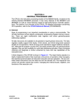
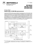
The MC68330 is a 32-bit integrated processor unit, combining high-performance data
manipulation capabilities with a variety of circuits typically used to integrate a processor
into the overall computer system. The MC68330 is a member of the M68300 Family of
modular devices featuring fully static, high-speed complementary metal-oxide
semiconductor (HCMOS) technology. Based on the powerful MC68020, the CPU32
central processing module of the MC68330 provides enhanced system performance and
uses the extensive software base of the M68000 Family. Figure 1-1 shows the major
components of the MC68330.
SIM40
INTERMODULE BUS
SYSTEM CONFIGURATI
AND PROTECTION
CLOCK SYNTHESIZE
CHIP SELECTS
AND WAIT STAT
CPU32
CORE PROCESSOR
EXTERNAL BU
INTERFACE
BUS ARBITRATION
IEEE TEST
Figure 1-1. Block Diagram
The MC68330 system integration module (SIM40) provides four chip selects that
enhance system integration for easy external memory or peripheral access. The CPU32
and SIM40 modules are connected on-chip via an intermodule bus (IMB).
The major features of the MC68330 are as follows:
• Integrated System Functions in a Single Chip
• 32-Bit M68000 Family Central Processor
— Upward User-Object-Code Compatible with the MC68000 and MC68010
— New Instructions for Embedded Control Applications
— Higher Performance Execution
• Four Programmable Chip-Select Signals
MOTOROLA
MC68330 USER’S MANUAL
For More Information On This Product,
Go to: www.freescale.com
1-1
Freescale Semiconductor, Inc...
Freescale Semiconductor, Inc.
• System Failure Protection:
— Software Watchdog Timer
— Periodic Interrupt Timer
— Spurious Interrupt, Double Bus Fault, and Bus Timeout Monitors
— Automatic Programmable Bus Termination
• Up to 16 Discrete I/O Pins
• Low-Power Operation:
— HCMOS Technology Reduces Power in Normal Operation
— LPSTOP Mode Provides Static State for Lower Standby Drain
• Frequency: 0–25 MHz at 5-V Supply, Software Programmable
• Package: 132-Pin Plastic Quad Flat Pack (PQFP)
1.1 CENTRAL PROCESSOR UNIT
The central processing unit of the MC68330 is the CPU32, an upward-compatible
M68000 Family member that excels in processing calculation-intensive algorithms and
supporting high-level languages. All MC68010 and most MC68020 enhancements, such
as virtual memory support, loop mode operation, instruction pipeline, and 32-bit
mathematical operations, are supported. Powerful addressing modes provide
compatibility with existing software programs and increase the efficiency of high-level
language compilers. New instructions, such as table lookup and interpolate and low
power stop, support the specific requirements for embedded control applications. Most
instructions can execute in half the number of clocks required by an MC68000, yielding
an overall 1.6 times performance of the same-speed MC68000.
1.2 SYSTEM INTEGRATION MODULE
The SIM40 includes an external interface and various functions that reduce the need for
external glue logic. The SIM40 contains system configuration and protection, the clock
synthesizer, four chip selects, and the external bus interface (EBI).
1.2.1 System Configuration and Protection
The system configuration and protection function controls system configuration and
provides maximum system safeguards. System protection is provided on the MC68330
by various monitors and timers, including the bus monitor, double bus fault monitor,
spurious interrupt monitor, software watchdog timer, and the periodic interrupt timer.
These system functions are integrated on the MC68330 to reduce board size and the
cost incurred with external components.
1.2.2 Clock Synthesizer
The system clock can be generated by an on-chip phase-locked loop (PLL) circuit to run
the device from a 32.768-kHz watch crystal. An external clock can also be used. The
system speed can be changed dynamically with the PLL, providing either high
performance or low power consumption under software control. With its fully static
HCMOS design, it is possible to completely stop the system clock in software while still
preserving the contents of the registers.
1-2
MC68330 USER’S MANUAL
For More Information On This Product,
Go to: www.freescale.com
MOTOROLA
Freescale Semiconductor, Inc.
1.2.3 Chip Selects
Four independent chip selects can enable external memory and peripheral circuits,
providing all handshaking and timing signals with up to 265-ns access times. Block size
is programmable in 256-byte increments up to the 4-Gbyte address capability. Accesses
can be preselected for either 8- or 16-bit transfers and up to three wait states.
1.2.4 External Bus Interface
Freescale Semiconductor, Inc...
Based on the MC68020 bus, the external bus provides 32 address lines and a 16-bit
data bus. The data bus allows dynamic sizing between 8- and 16-bit data accesses.
External bus arbitration is accomplished by a four-line handshaking interface. Strobe
signals provide easy byte-write capability. Transfers can be made in as little as two clock
cycles.
MOTOROLA
MC68330 USER’S MANUAL
For More Information On This Product,
Go to: www.freescale.com
1-3
Freescale Semiconductor, Inc.
SECTION 2
SIGNAL DESCRIPTIONS
This section contains brief descriptions of the MC68330 input and output signals in their
functional groups as shown in Figure 2-1.
Freescale Semiconductor, Inc...
2.1 SIGNAL INDEX
The input and output signals for the MC68330 are listed in Table 2-1. The name,
mnemonic, and brief functional description are presented. For more detail on each signal,
refer to the paragraph named for the signal. Guaranteed timing specifications for the
signals listed in Table 2-1 can be found in MC68330/D, MC68330 Technical Summary.
2.2 ADDRESS BUS
The address bus consists of the following two groups. Refer to 3.1.3 Address Bus for
information on the address bus and its relationship to bus operation.
2.2.1 Address Bus (A23–A0)
These three-state outputs (along with A31–A24) provide the address for the current bus
cycle, except in the CPU address space. Refer to 3.4 CPU Space Cycles for more
information on the CPU address space. A23 is the most significant address signal in this
group.
2.2.2 Address Bus (A31–A24)
These pins can be programmed as the most significant eight address bits, port A parallel
I/O, or interrupt acknowledge strobes. These pins can be used for more than one of their
multiplexed functions as long as the external demultiplexing circuit properly resolves
collisions between the different functions.
A31–A24. These pins can function as the most significant eight address bits. A31 is the
most significant address signal in this group.
Port A7–Port A0. These eight pins can serve as a dedicated parallel I/O port. See 4.2.5.1
Port A for more information on programming these pins.
IACK7–IACK1 . The MC68330 asserts one of these pins to indicate the level of an
external interrupt during an interrupt acknowledge (IACK) cycle. Peripherals can use the
IACK strobes instead of monitoring the address bus and function codes to determine that
an IACK cycle is in progress and to obtain the current interrupt level. See 3.4.4 Interrupt
Acknowledge Bus Cycles for more information. Only seven of these eight pins are used
as IACK strobe outputs since there is no IACK0 strobe.
MOTOROLA
MC68330 USER’S MANUAL
For More Information On This Product,
Go to: www.freescale.com
2-1
Freescale Semiconductor, Inc.
A31/PORT A7/IA
A30/PORT A6/IA
A29/PORT A5/IA
A28/PORT A4/IA
A27/PORT A3/IA
A26/PORT A2/IA
A25/PORT A1/IA
A24/PORT
A23–A
TEST
D15–D
FC2–FC0
Freescale Semiconductor, Inc...
RESET
BERR
HALT
AS
DS
R/W
SIZ1
SIZ0
DSACK
DSACK0
UWE
LWE
CS3
CS2
CS1
AVEC/CS
BR
BG
BGACK
RMC
IPIPE
IFETCH
BKPT
FREEZE
PORT A
TCK
TMS
TDI
TDO
EXTERNAL
BUS
INTERFACE
SYSTEM
INTEGRATION
MODULE
INTERMODULE BUS
CPU32
CORE
PROCESSOR
CHIP
SELECT
BUS
ARBITRATION
IRQ7/PORT B
IRQ6/PORT B
IRQ5/PORT B
IRQ4/PORT B
IRQ3/PORT B3
IRQ2/PORT B2
IRQ1/PORT B1
MODCK/PORT
CLOCK
CLKOUT
XTAL
EXTAL
XFC
PORT B
Figure 2-1. Functional Signal Groups
2-2
MC68330 USER’S MANUAL
For More Information On This Product,
Go to: www.freescale.com
MOTOROLA
Freescale Semiconductor, Inc.
Table 2-1. Signal Index
Signal Name
Address Bus
Address Bus/ Port A7–A0/ IACK7–
IACK1
Data Bus
Function Codes
Mnemonic
A23–A0
A31–A24
Chip Select /AVEC
CS3–CS0
BR
BG
Bus Request
Bus Grant
Freescale Semiconductor, Inc...
D15–D0
FC2–FC0
BGACK
Bus Grant Acknowledge
DSACK1,
DSACK0
UWE, LWE
Data and Size Acknowledge
Byte Write Enable
RMC
Read-Modify-Write Cycle
AS
DS
Address Strobe
Data Strobe
Size
SIZ1, SIZ0
R/ W
IRQ7 – IRQ1
Read/Write
Interrupt Request Level/
Port B7 – B1
Reset
Halt
Bus Error
System Clock Out
Crystal Oscillator
RESET
HALT
BERR
CLKOUT
EXTAL, XTAL
External Filter Capacitor
XFC
Clock Mode Select/Port B0
MODCK
Instruction Fetch
IFETCH
Instruction Pipe
Breakpoint
Freeze
IPIPE
BKPT
FREEZE
Test Clock
Test Mode Select
Test Data In
Test Data Out
Synchronizer Power
TCK
TMS
TDI
TDO
VCCSYN
System Power Supply and Return
MOTOROLA
VCC , GND
Function
Lower 24 bits of address bus
Upper eight bits of address bus, parallel I/O port, or interrupt
acknowledge lines
16-bit data bus used to transfer byte or word data
Identifies the processor state and the address space of the
current bus cycle
Enables peripherals at programmed addresses or provides
automatic vector request (CS0) during an interrupt
acknowledge cycle
Indicates that an external device requires bus mastership
Indicates that current bus cycle is complete and the
MC68330 has relinquished the bus
Indicates that an external device has assumed bus
mastership
Provides asynchronous data transfers and dynamic bus
sizing
Provides an enable signal for byte writes to external devices,
when using a 16-bit port
Identifies the bus cycle as part of an indivisible read-modifywrite operation
Indicates that a valid address is on the address bus
During a read cycle, DS indicates that an external device
should place valid data on the data bus. During a write cycle,
DS indicates that valid data is on the data bus.
Indicates the number of bytes remaining to be transferred for
this cycle
Indicates the direction of data transfer on the bus
Provides an interrupt priority level to the CPU32 or provides
parallel I/O
System reset
Suspend external bus activity
Indicates an erroneous bus operation is being attempted
Internal system clock output
Connections for an external crystal to the internal oscillator
circuit
Connection pin for an external capacitor to filter the circuit of
the phase-locked loop
Selects the source of the internal system clock or furnishes a
parallel I/O bit
Indicates when the CPU32 is performing an instruction word
prefetch and when the instruction pipeline has been flushed
Tracks movement of words through the instruction pipeline
Signals a hardware breakpoint to the CPU32
Indicates that the CPU32 has entered background debug
mode
Provides a clock for IEEE 1149.1 test logic
Controls test mode operations
Shifts in test instructions and test data
Shifts out test instructions and test data
Quiet power supply to VCO; also used to control synthesizer
mode after reset.
Power supply and return to the MC68330
MC68330 USER’S MANUAL
For More Information On This Product,
Go to: www.freescale.com
2-3
Freescale Semiconductor, Inc.
2.3 DATA BUS (D15–D0)
These three-state bidirectional signals provide the general-purpose data path between the
MC68330 and all other devices. Although the data path is a maximum of 16 bits wide, it
can be dynamically sized to support 8- or 16-bit transfers. D15 is the most significant bit of
the data bus. Refer to 3.1.5 Data Bus for information on the data bus and its relationship
to bus operation.
2.4 FUNCTION CODES (FC2–FC0)
These three-state outputs identify the processor state and the address space of the
current bus cycle, as listed in Table 2-2. Refer to 3.1.2 Function Codes and 3.4 CPU
Space Cycles for more information.
Freescale Semiconductor, Inc...
NOTE
Since FC3 is not implemented, the programmer must set
FC3 and FCM3 to zero in the chip-select base address
and address mask registers.
Table 2-2. Function Codes
3
0
0
0
0
0
0
0
0
Function Code Bits
2
1
0
0
0
0
0
0
1
0
1
0
0
1
1
1
0
0
1
0
1
1
1
0
1
1
1
Address Spaces
Reserved (Motorola)
User Data Space
User Program Space
Reserved (User )
Reserved (Motorola)
Supervisor Data Space
Supervisor Program Space
Supervisor CPU Space
2.5 CHIP SELECTS ( CS3– CS0)
These pins are chip-select output signals. The CS0 pin can also be programmed as an
autovector input.
CS3 – CS0. The chip-select output signals enable peripherals at programmed addresses.
CS0 is the chip select for a ROM containing the user's reset vector and initialization
program; therefore, it functions as the boot chip select immediately after reset. Refer to
4.2.4 Chip-Select Submodule for more information on chip selects.
AVEC. This signal requests an automatic vector during an interrupt acknowledge cycle.
Refer to 3.4.4.2 Autovector Interrupt Acknowledge Cycle and 4.3.2.2 Autovector
Register for more information on the autovector function.
2-4
MC68330 USER’S MANUAL
For More Information On This Product,
Go to: www.freescale.com
MOTOROLA
Freescale Semiconductor, Inc.
2.6 INTERRUPT REQUEST LEVEL ( IRQ7 – IRQ1)
These pins can be programmed to be either prioritized interrupt request lines or port B
parallel I/O.
IRQ7 – IRQ1 . IRQ7, the highest priority, is nonmaskable. IRQ6–IRQ1 are internally
maskable interrupts. Refer to Section 5 CPU32 for more information on interrupt request
lines.
Port B7 – B0. These pins can be used as port B parallel I/O. Refer to 4.2.5.2 Port B
registers for more information on parallel I/O signals.
Freescale Semiconductor, Inc...
2.7 BUS CONTROL SIGNALS
These signals control the bus transfer operations of the MC68330.
2.7.1 Data and Size Acknowledge ( DSACK1, DSACK0)
These two active-low input signals allow asynchronous data transfers and dynamic data
bus sizing between the MC68330 and external devices as listed in Table 2-3. Refer to
3.1.7 Bus Cycle Termination Signals for more information on these signals and their
relationship to dynamic bus sizing.
Table 2-3. DSACKx Codes and Results
DSACK1
1
(Negated)
1
(Negated)
0
(Asserted)
0
(Asserted)
DSACK0
1
(Negated)
0
(Asserted)
1
(Negated)
0
(Asserted)
Result
Insert Wait States in Current Bus Cycle
Complete Cycle – Data Bus Port Size Is 8 Bits
Complete Cycle –Data Bus Port Size Is 16 Bits
Reserved –Defaults to 16 Bit Port Size
2.7.2 Autovector (AVEC)
See 2.5 Chip Selects (CS3–CS0) .
2.7.3 Address Strobe ( AS)
This output signal is driven by the bus master to indicate a valid address on the address
bus. The function code, size, and read/write signals are also valid when AS is asserted.
Refer to 3.1.4 Address Strobe for information about the relationship of AS to bus
operation.
2.7.4 Data Strobe (DS)
During a read cycle, this output signal is driven by the bus master to indicate that an
external device should place valid data on the data bus. During a write cycle, the data
strobe indicates that valid data is on the data bus. Refer to 3.1.6 Data Strobe for
information about the relationship of DS to bus operation.
MOTOROLA
MC68330 USER’S MANUAL
For More Information On This Product,
Go to: www.freescale.com
2-5
Freescale Semiconductor, Inc.
2.7.5 Transfer Size (SIZ1, SIZ0)
These output signals are driven by the bus master to indicate the number of operand
bytes remaining to be transferred in the current bus cycle (see Table 2-4). Refer to 3.2.1
Dynamic Bus Sizing for more information.
Table 2-4. Size Signal
Encoding
Freescale Semiconductor, Inc...
SIZ1
0
1
1
0
SIZ0
1
0
1
0
Transfer Size
Byte
Word
3 Byte
Long Word
2.7.6 Read/Write (R/ W)
This active-high output signal is driven by the bus master to indicate the direction of data
transfer on the bus. A logic one indicates a read from a slave device; a logic zero indicates
a write to a slave device. Refer to 3.1.1 Bus Control Signals for more information.
2.8 BUS ARBITRATION SIGNALS
The following signals are the four bus arbitration control signals used to determine the bus
master.
2.8.1 Bus Request (BR)
This active-low input signal indicates that an external device needs to become the bus
master. This input is typically wire-ORed. Refer to 3.6 Bus Arbitration for more
information.
2.8.2 Bus Grant (BG)
Assertion of this active-low output signal indicates that the bus master has relinquished
the bus. Refer to 3.6.2 Bus Grant for more information.
2.8.3 Bus Grant Acknowledge (BGACK)
Assertion of this active-low input indicates that an external device has become the bus
master. Refer to 3.6.3 Bus Grant Acknowledge for more information.
2.8.4 Read-Modify-Write Cycle (RMC)
This output signal identifies the bus cycle as part of an indivisible read-modify-write
operation; it remains asserted during all bus cycles of the read-modify-write operation to
indicate that bus ownership cannot be transferred. Refer to 3.3.3 Read-Modify-Write
Cycle for additional information.
2-6
MC68330 USER’S MANUAL
For More Information On This Product,
Go to: www.freescale.com
MOTOROLA
Freescale Semiconductor, Inc.
2.8.5 Byte Write Enable ( UWE, LWE)
On a write cycle to a 16-bit port, these active-low output signals indicate when the upper
or lower eight bits of the data bus contain valid data. See 3.1.7 Byte Write Enable for a
description of byte write enable operation.
2.9 EXCEPTION CONTROL SIGNALS
These signals are used by the integrated processor unit to recover from an exception.
Freescale Semiconductor, Inc...
2.9.1 Reset ( RESET)
This active-low, open-drain, bidirectional signal is used to initiate a system reset. An
external reset signal (as well as a reset from the SIM) resets the MC68330 as well as all
external devices. A reset signal from the CPU32 (asserted as part of the RESET
instruction) resets external devices only — the internal state of the CPU32 is not affected;
other on-chip modules are reset, but the configuration is not altered. When asserted by the
MC68330, this signal is guaranteed to be asserted for a minimum of 512 clock cycles.
Refer to 3.7 Reset Operation for a description of bus reset operation and Section 5
CPU32 for information about the reset exception.
2.9.2 Halt (HALT)
This active-low, open-drain, bidirectional signal is asserted to suspend external bus
activity, to request a retry when used with BERR, or to perform a single-step operation. As
an output, HALT indicates a double bus fault by the CPU32. Refer to 3.5 Bus Exception
Control Cycles for a description of the effects of HALT on bus operation.
2.9.3 Bus Error (BERR)
This active-low input signal indicates that an invalid bus operation is being attempted or,
when used with HALT, that the processor should retry the current cycle. Refer to 3.5 Bus
Exception Control Cycles for a description of the effects of BERR on bus operation.
2.10 CLOCK SIGNALS
These signals are used by the MC68330 for controlling or generating the system clocks.
Refer to 4.2.3 Clock Synthesizer for more information on the various clock signals.
2.10.1 System Clock (CLKOUT)
This output signal is the system clock and is used as the bus timing reference by external
devices. CLKOUT can be slowed in low-power stop mode. See 4.3.3 Clock Synthesizer
Control Register (SYNCR) for more information.
2.10.2 Crystal Oscillator (EXTAL, XTAL)
These two pins are the connections for an external crystal to the internal oscillator circuit.
If an external oscillator is used, it should be connected to EXTAL, with XTAL left open.
See 4.2.3 Clock Synthesizer for more information.
2.10.3 External Filter Capacitor (XFC)
MOTOROLA
MC68330 USER’S MANUAL
For More Information On This Product,
Go to: www.freescale.com
2-7
Freescale Semiconductor, Inc.
This pin is used to add an external capacitor to the filter circuit of the phase-locked loop.
The capacitor should be connected between XFC and VCCSYN .
2.10.4 Clock Mode Select (MODCK)
This pin selects the source of the internal system clock during reset. After reset, it can be
programmed to be port B parallel I/O.
MODCK. The state of this active-high input signal during reset selects the source of the
internal system clock. If MODCK is high during reset, the internal voltage-controlled
oscillator (VCO) furnishes the system clock. If MODCK is low during reset, an external
frequency appearing at the EXTAL pin furnishes the system clock.
Freescale Semiconductor, Inc...
Port B0. This pin can be used as port B parallel I/O. Refer to 4.2.5.2 PORT B for more
information on parallel I/O signals.
2.11 INSTRUMENTATION AND EMULATION SIGNALS
These signals are used for test or software debugging.
2.11.1 Instruction Fetch ( IFETCH)
This active-low output signal indicates when the CPU32 is performing an instruction word
prefetch and when the instruction pipeline has been flushed. Refer to Section 5 CPU32
for information about IFETCH.
2.11.2 Instruction Pipe (IPIPE)
This active-low output signal is used to track movement of words through the instruction
pipeline. Refer to Section 5 CPU32 for information about IPIPE.
2.11.3 Breakpoint (BKPT)
This active-low input signal is used to signal a hardware breakpoint to the CPU32. Refer to
Section 5 CPU32 for information about BKPT.
2.11.4 Freeze (FREEZE)
Assertion of this active-high output signal indicates the CPU32 has acknowledged a
breakpoint and has initiated background mode operation. See Section 5 CPU32 for more
information about FREEZE and background mode.
2.12 TEST SIGNALS
The following signals are used with the onboard test logic defined by the IEEE 1149.1
standard. See Section 6 IEEE 1149.1 Test Access Port for more information on the use
of these signals.
2.12.1 Test Clock (TCK)
This input provides a clock for onboard test logic defined by the IEEE 1149.1 standard.
2-8
MC68330 USER’S MANUAL
For More Information On This Product,
Go to: www.freescale.com
MOTOROLA
Freescale Semiconductor, Inc.
2.12.2 Test Mode Select (TMS)
This input controls test mode operations for onboard test logic defined by the IEEE 1149.1
standard.
2.12.3 Test Data In (TDI)
This input is used for serial test instructions and test data for onboard test logic defined by
the IEEE 1149.1 standard.
2.12.4 Test Data Out (TDO)
Freescale Semiconductor, Inc...
This output is used for serial test instructions and test data for onboard test logic defined
by the IEEE 1149.1 standard.
2.13 SYNTHESIZER POWER (V CCSYN )
This pin supplies a quiet power source to the VCO to provide greater frequency stability
and is also used to select clock modes (see Section 4 System Integration Module).
2.14 SYSTEM POWER AND GROUND (V CC AND GND)
These pins provide system power and return to the MC68330. Multiple pins are provided
for adequate current capability. All power supply pins must have adequate bypass
capacitance for high-frequency noise suppression.
2.15 SIGNAL SUMMARY
Table 2-5 presents a summary of all the signals discussed in the preceding paragraphs.
MOTOROLA
MC68330 USER’S MANUAL
For More Information On This Product,
Go to: www.freescale.com
2-9
Freescale Semiconductor, Inc.
Table 2-5. Signal Summary
Signal Name
Address Bus
Address Bus/ Port A7–A0/
IACK7-IACK1
Data Bus
Function Codes
Chip Select/ AVEC
Freescale Semiconductor, Inc...
Bus Request
Bus Grant
Bus Grant Acknowledge
Data and Size Acknowledge
Read-Modify-Write Cycle
Address Strobe
Data Strobe
Byte Write Enable
Size
Read/Write
Interrupt Request Level/Port B7 – B1
Reset
Halt
Bus Error
System Clock Out
Crystal Oscillator
Crystal Oscillator
External Filter Capacitor
Clock Mode Select/Port B0
Instruction Fetch
Instruction Pipe
Breakpoint
Freeze
Test Clock
Test Mode Select
Test Data In
Test Data Out
Synchronizer Power
System Power Supply and Return
2-10
Mnemonic
A23–A0
A31–A24
D15–D0
FC3–FC0
CS3–CS0
BR
BG
BGACK
DSACK1, DSACK0
RMC
AS
DS
UWE, LWE
SIZ1, SIZ0
R/ W
IRQ7 – IRQ1
RESET
HALT
BERR
CLKOUT
EXTAL
XTAL
XFC
MODCK
IFETCH
IPIPE
BKPT
FREEZE
TCK
TMS
TDI
TDO
V CCSYN
V CC, GND
Input/
Output
Out
Out/I/O/
Out
I/O
Out
Out/
In
In
Out
In
In
Out
Out
Out
Out
Out
Out
In/I/O
I/O
I/O
In
Out
In
Out
In
In/I/O
Out
Out
In
Out
In
In
In
Out
–
–
MC68330 USER’S MANUAL
For More Information On This Product,
Go to: www.freescale.com
Active
State
–
–/–/Low
ThreeState
Yes
Yes
–
–
Low/
Low
Low
Low
Low
Low
Low
Low
Low
Low
–
High/Low
Low/–
Low
Low
Low
–
–
–
–
–/–
Low
Low
Low
High
–
High
High
High
–
–
Yes
Yes
No
–
No
–
–
Yes
Yes
Yes
Yes
Yes
Yes
–
No
No
–
No
–
–
–
–
Yes
No
–
No
–
–
–
–
–
–
MOTOROLA
Freescale Semiconductor, Inc.
Freescale Semiconductor, Inc...
SECTION 3
BUS OPERATION
This section provides a functional description of the bus, the signals that control it, and the
bus cycles provided for data transfer operations. It also describes the error and halt
conditions, bus arbitration, and reset operation. Operation of the external bus is the same
whether the MC68330 or an external device is the bus master; the names and
descriptions of bus cycles are from the viewpoint of the bus master. For exact timing
specifications, refer to MC68330/D, MC68330 Technical Summary.
The MC68330 architecture supports byte, word, and long-word operands allowing access
to 8- and 16-bit data ports through the use of asynchronous cycles controlled by the size
outputs (SIZ1, SIZ0) and data size acknowledge inputs (DSACK1, DSACK0 ). The
MC68330 requires word and long-word operands to be located in memory on word
boundaries. The only type of transfer that can be performed to an odd address is a singlebyte transfer, referred to as an odd-byte transfer. For an 8-bit port, multiple bus cycles
may be required for an operand transfer due to either misalignment or a word or long-word
operand.
3.1 BUS TRANSFER SIGNALS
The bus transfers information between the MC68330 and external memory or a peripheral
device. External devices can accept or provide 8 bits or 16 bits in parallel and must follow
the handshake protocol described in this section. The maximum number of bits accepted
or provided during a bus transfer is defined as the port width. The MC68330 contains an
address bus that specifies the address for the transfer and a data bus that transfers the
data. Control signals indicate the beginning and type of the cycle as well as the address
space and size of the transfer. The selected device then controls the length of the cycle
with the signal(s) used to terminate the cycle. Strobe signals, one for the address bus and
another for the data bus, indicate the validity of the address and provide timing information
for the data. Both asynchronous and synchronous operation is possible for any port width.
In asynchronous operation, the bus and control input signals are internally synchronized to
the MC68330 clock, introducing a delay. This delay is the time required for the MC68330
to sample an input signal, synchronize the input to the internal clocks, and determine
whether it is high or low. In synchronous mode, the bus and control input signals must be
timed to setup and hold times. Since no synchronization is needed, bus cycles can be
completed in three clock cycles in this mode. Additionally, using the fast-termination option
of the chip-select signals, two-clock operation is possible.
Furthermore, for all inputs, the MC68330 latches the level of the input during a sample
window around the falling edge of the clock signal. This window is illustrated in Figure 3-1,
where t su and t h are the input setup and hold times, respectively. To ensure that an input
signal is recognized on a specific falling edge of the clock, that input must be stable during
the sample window. If an input makes a transition during the window time period, the level
MOTOROLA
MC68330 USER’S MANUAL
For More Information On This Product,
Go to: www.freescale.com
3-1
Freescale Semiconductor, Inc.
recognized by the MC68330 is not predictable; however, the MC68330 always resolves
the latched level to either a logic high or low before using it. In addition to meeting input
setup and hold times for deterministic operation, all input signals must obey the protocols
described in this section.
t su
th
CLKOUT
Freescale Semiconductor, Inc...
EXT
SAMPLE WINDO
Figure 3-1. Input Sample Window
3.1.1 Bus Control Signals
The MC68330 initiates a bus cycle by driving the address, size, function code and
read/write outputs. At the beginning of a bus cycle, SIZ1 and SIZ0 are driven with the
function code signals. SIZ1 and SIZ0 indicate the number of bytes remaining to be
transferred during an operand cycle (consisting of one or more bus cycles). Table 3-1 lists
the encoding of SIZ1 and SIZ0. These signals are valid while address strobe ( AS ) is
asserted. The read/write (R/W) signal determines the direction of the transfer during a bus
cycle. Driven at the beginning of a bus cycle, R/W is valid while AS is asserted. R/ W only
transitions when a write cycle is preceded by a read cycle or vice versa. The signal may
remain low for consecutive write cycles. The read-modify-write cycle ( RMC ) signal is
asserted at the beginning of the first bus cycle of a read-modify-write operation and
remains asserted until completion of the final bus cycle of the operation.
Table 3-1. Size Signal Encoding
SIZ1
SIZ0
Transfer Size
0
1
Byte
1
0
Word
1
1
3 Byte
0
0
Long-word
3.1.2 Function Codes
The function code signals (FC2–FC0) are outputs that indicate one of eight address
spaces to which the address applies. Seven of these spaces are designated as either user
or supervisor, and program or data spaces. One other address space is designated as
CPU space to allow the CPU32 to acquire specific control information not normally
3-2
MC68330 USER’S MANUAL
For More Information On This Product,
Go to: www.freescale.com
MOTOROLA
Freescale Semiconductor, Inc.
associated with read or write bus cycles. The function code signals are valid while AS is
asserted.
Function codes (see Table 3-2) can be considered as extensions of the 32-bit address that
can provide up to eight different 4-Gbyte address spaces. Function codes are
automatically generated by the CPU32 to select address spaces for data and program at
both user and supervisor privilege levels, and a CPU address space for processor
functions. User programs access only their own program and data areas to increase
protection of system integrity and can be restricted from accessing other information. The
S-bit in the CPU32 status register is set for supervisor accesses and cleared for user
accesses to provide differentiation. Refer to 3.4 CPU Space Cycles for more information.
Freescale Semiconductor, Inc...
Table 3-2. Address Space Encoding
Function Code Bits
Address Spaces
2
1
0
0
0
0
Reserved (Motorola)
0
0
1
User Data Space
0
1
0
User Program Space
0
1
1
Reserved (User )
1
0
0
Reserved (Motorola)
1
0
1
Supervisor Data Space
1
1
0
Supervisor Program Space
1
1
1
Supervisor CPU Space
3.1.3 Address Bus (A31-A0)
The address bus signals are outputs that define the address of the byte (or the most
significant byte) to be transferred during a bus cycle. The MC68330 places the address on
the bus at the beginning of a bus cycle. The address is valid while AS is asserted.
3.1.4 Address Strobe ( AS)
AS is an output timing signal that indicates the validity of an address on the address bus
and of many control signals. AS is asserted approximately one-half clock cycle after the
beginning of a bus cycle.
3.1.5 Data Bus (D15-D0)
The data bus is a bidirectional, nonmultiplexed, parallel bus that contains the data being
transferred to or from the MC68330. A read or write operation may transfer 8 or 16 bits of
data (one or two bytes) in one bus cycle. During a read cycle, the data is latched by the
MC68330 on the last falling edge of the clock for that bus cycle. For a write cycle, all 16
bits of the data bus are driven, regardless of the port width or operand size. The MC68330
places the data on the data bus approximately one-half clock cycle after AS is asserted in
a write cycle.
3.1.6 Data Strobe (DS)
MOTOROLA
MC68330 USER’S MANUAL
For More Information On This Product,
Go to: www.freescale.com
3-3
Freescale Semiconductor, Inc.
The data strobe is an output timing signal that applies to the data bus. For a read cycle,
the MC68330 asserts DS and AS simultaneously to signal the external device to place
data on the bus. For a write cycle, DS signals to the external device that the data to be
written is valid on the bus. The MC68330 asserts DS approximately one clock cycle after
the assertion of AS during a write cycle.
3.1.7 Byte Write Enable ( UWE, LWE)
Freescale Semiconductor, Inc...
The upper write enable ( UWE) indicates that the upper eight bits of the data bus contains
valid data during a write cycle. The lower write enable (LWE) indicates that the lower eight
bits of the data bus contains valid data during a write cycle. The equations of the byte
write enables are as follows:
UWE = R/ W + AS + A0
LWE = R/ W + AS + (A0 × SIZ0)
These signals have the same timing as AS , and are only valid when writing to a 16-bit
port.
3.1.8 Bus Cycle Termination Signals
The following signals can terminate a bus cycle.
3.1.8.1 DATA TRANSFER AND SIZE ACKNOWLEDGE SIGNALS (DSACK1 AND
DSACK0). During bus cycles, external devices assert DSACK1 and/or DSACK0 as part
of the bus protocol. During a read cycle, this signals the MC68330 to terminate the bus
cycle and to latch the data. During a write cycle, this indicates that the external device has
successfully stored the data and that the cycle may terminate. These signals also indicate
to the MC68330 the size of the port for the bus cycle just completed (see Table 3-3). Refer
to 3.3.1 Read Cycle for timing relationships of DSACK1 and DSACK0.
Additionally, the system integration module (SIM40) can be programmed to internally
generate DSACK1 and DSACK0 for external accesses, eliminating logic required to
generate these signals. The SIM40 can alternatively be programmed to generate a fast
termination, providing a two-cycle external access. Refer to 3.2.6 Fast-Termination
Cycles for additional information on these cycles.
3.1.8.2 BUS ERROR (BERR). This signal is also a bus cycle termination indicator and can
be used in the absence of DSACKx to indicate a bus error condition. BERR can also be
asserted in conjunction with DSACKx to indicate a bus error condition, provided it meets
the appropriate timing described in this section and in MC68330/D, MC68330 Technical
Summary . Additionally, BERR and HALT can be asserted together to indicate a retry
termination. Refer to 3.5 Bus Exception Control Cycles for additional information on the
use of these signals.
The internal bus monitor can be used to generate the BERR signal for internal and
internal-to-external transfers in all the following descriptions. If the bus cycles of an
external bus master are to be monitored, external BERR generation must be provided
since the internal BERR monitor has no information about transfers initiated by an external
bus master.
3-4
MC68330 USER’S MANUAL
For More Information On This Product,
Go to: www.freescale.com
MOTOROLA
Freescale Semiconductor, Inc.
3.1.8.3 AUTOVECTOR (AVEC ). This signal can be used to terminate interrupt
acknowledge cycles, indicating that the MC68330 should internally generate a vector
(autovector) number to locate an interrupt handler routine. AVEC can be generated either
externally or internally by the SIM40 (refer to Section 4 System Integration Module for
additional information). AVEC is ignored during all other bus cycles.
3.2 DATA TRANSFER MECHANISM
Freescale Semiconductor, Inc...
The MC68330 supports byte, word, and long-word operands, allowing access to 8- and
16-bit data ports through the use of asynchronous cycles controlled by DSACK1 and
DSACK0 . The MC68330 also supports byte, word, and long-word operands, allowing
access to 8- and 16-bit data ports through the use of synchronous cycles controlled by the
fast-termination capability of the SIM40.
3.2.1 Dynamic Bus Sizing
The MC68330 dynamically interprets the port size of the addressed device during each
bus cycle, allowing operand transfers to or from 8- and 16-bit ports. During an operand
transfer cycle, the slave device signals its port size (byte or word) and indicates
completion of the bus cycle to the MC68330 through the use of the DSACKx inputs. Refer
to Table 3-3 for DSACKx encodings.
Table 3-3. DSACKx Encodings
DSACK1
DSACK0
1
(Negated)
1
(Negated)
0
(Asserted)
0
(Asserted)
1
(Negated)
0
(Asserted)
1
(Negated)
0
(Asserted)
Result
Insert Wait States in Current Bus Cycle
Complete Cycle — Data Bus Port Size is 8 Bits
Complete Cycle — Data Bus Port Size is 16 Bits
Reserved — Defaults to 16-Bit Port Size
For example, if the MC68330 is executing an instruction that reads a long-word operand
from a 16-bit port, the MC68330 latches the 16 bits of valid data and runs another bus
cycle to obtain the other 16 bits. The operation from an 8-bit port is similar, but requires
four read cycles. The addressed device uses DSACKx to indicate the port width. For
instance, a 16-bit device always returns DSACKx for a 16-bit port (regardless of whether
the bus cycle is a byte or word operation).
Dynamic bus sizing requires that the portion of the data bus used for a transfer to or from
a particular port size be fixed. A 16-bit port must reside on data bus bits 15–0, and an 8-bit
port must reside on data bus bits 15–8. This requirement minimizes the number of bus
cycles needed to transfer data to 8- and 16-bit ports and ensures that the MC68330
correctly transfers valid data.
The UWE/LWE signals are only valid for a 16-bit port width. Since an 8-bit port must
reside on data bus bits 15-8, the UWE/LWE signals are not required. AS or CS should be
used for an 8-bit port.
MOTOROLA
MC68330 USER’S MANUAL
For More Information On This Product,
Go to: www.freescale.com
3-5
Freescale Semiconductor, Inc.
Freescale Semiconductor, Inc...
The MC68330 always attempts to transfer the maximum amount of data on all bus cycles;
for a word operation, it always assumes that the port is 16 bits wide when beginning the
bus cycle. The bytes of operands are designated as shown in Figure 3-2. The most
significant byte of a long-word operand is OP0, and OP3 is the least significant byte. The
two bytes of a word-length operand are OP0 (most significant) and OP1. The single byte
of a byte-length operand is OP0. These designations are used in the figures and
descriptions that follow.
Figure 3-2 shows the required organization of data ports on the MC68330 bus for both 8and 16-bit devices. The four bytes shown in Figure 3-2 are connected through the internal
data bus and data multiplexer to the external data bus. The data multiplexer establishes
the necessary connections for different combinations of address and data sizes. The
multiplexer takes the two bytes of the 16-bit bus and routes them to their required
positions. The positioning of bytes is determined by the size (SIZ1 and SIZ0) and address
(A0) outputs. The SIZ1 and SIZ0 outputs indicate the number of bytes to be transferred
during the current bus cycle, as listed in Table 3-1. The number of bytes transferred during
a write or read bus cycle is equal to or less than the size indicated by the SIZ1 and SIZ0
outputs, depending on port width. For example, during the first bus cycle of a long-word
transfer to a word port, the size outputs indicate that four bytes are to be transferred
although only two bytes are moved on that bus cycle.
The address line A0 also affects the operation of the data multiplexer. During an operand
transfer, A31–A1 indicate the word base address of that portion of the operand to be
accessed, and A0 indicates the byte offset from the base (i.e., either odd or even byte).
Figure 3-2 lists the bytes required on the data bus for read cycles. The entries shown as
OPn are portions of the requested operand that are read or written during that bus cycle
and are defined by SIZ1, SIZ0, and A0 for the bus cycle. The transfer cases marked
misaligned are not generated by the MC68330.
3-6
MC68330 USER’S MANUAL
For More Information On This Product,
Go to: www.freescale.com
MOTOROLA
Freescale Semiconductor, Inc.
OP0
OPERAND
OP1
OP0
31
OP2
OP1
OP0
23
OP3
OP2
OP1
OP0
15
7
Freescale Semiconductor, Inc...
Case
(a)
(b)
(c)
(d)
(e)
(f)
(g)
(h)
(i)
(j)
(k)
(l)
(m)
(n)
(o)
Transfer Ca
SIZ1
Byte to By
0
0
Byte to Word (Ev
Byte to Word (O
0
Word to Byte (Align
1
1
Word to Byte (Misalig
1
Word to Word (Alig
Word to Word (Misalig
1
3 Byte to Byte (Align
1
1
3 Byte to Byte (Misalig
1
3 Byte to Word (Align
3 Byte to Word (Misalig
1
Long Word to Byte (Alig
0
Long Word to Byte (Misalig 0
0
Long Word to Word (Ali
Long Word to Word (Misali 0
SIZ0
1
1
1
0
0
0
0
1
1
1
1
0
0
0
0
A0
X
0
1
0
1
0
1
0
1
0
1
0
1
0
1
DSACK DSACK
1
0
0
X
0
X
1
0
1
0
0
X
0
X
1
0
1
0
0
X
0
X
1
0
1
0
0
X
0
X
0
Data Bu
D15
D8 D7
D0
OP0
(OP0
OP0
(OP0
(OP0
OP0
OP0
(OP1
(OP0
OP0
OP0
OP1
(OP0
OP0
OP0
(OP1
OP0
(OP0
OP0
OP1
(OP0
OP0
OP0
(OP1
OP0
(OP0
OP0
OP1
(OP0
OP0
NOTES:
1.Operands in parentheses are ignored by the MC68330 during read cycles.
2. Misaligned and 3 byte transfer cases, identified by an asterisk, are not supported by the MC68330.
3. A 3-byte to byte transfer does occur as the second byte transfer of a long-word to byte port transfer.
Figure 3-2. MC68330 Interface to Various Port Sizes
3.2.2 Misaligned Operands
In this architecture, the basic operand size is 16 bits. Operand misalignment refers to
whether an operand is aligned on a word boundary or overlaps the word boundary,
determined by address line A0. When A0 is low, the address is even and is a word and
byte boundary. When A0 is high, the address is odd and is a byte boundary only. A byte
operand is properly aligned at any address; a word or long-word operand is misaligned at
an odd address.
At most, each bus cycle can transfer a word of data aligned on a word boundary. If the
MC68330 transfers a long-word operand over a 16-bit port, the most significant operand
word is transferred on the first bus cycle, and the least significant operand word is
transferred on a following bus cycle.
The CPU32 restricts all operands (both data and instructions) to be aligned. That is, word
and long-word operands must be located on a word or long-word boundary, respectively.
The only type of transfer that can be performed to an odd address is a single-byte transfer,
referred to as an odd-byte transfer. If a misaligned access is attempted, the CPU32
generates an address error exception, and enters exception processing. Refer to Section
5 CPU32 for more information on exception processing.
MOTOROLA
MC68330 USER’S MANUAL
For More Information On This Product,
Go to: www.freescale.com
3-7
Freescale Semiconductor, Inc.
3.2.3 Operand Transfer Cases
The following cases are examples of the allowable alignments of operands to ports.
3.2.3.1 BYTE OPERAND TO 8-BIT PORT, ODD OR EVEN (A0 = X). The MC68330
drives the address bus with the desired address and the size pins to indicate a single-byte
operand.
BYTE OPERAN
OP0
0
7
Freescale Semiconductor, Inc...
DATA BU
CYCLE
D8 D7
D0
D15
OP0
(OP0
SIZ
0
SIZ0
1
A0
X
DSACK DSACK
1
0
For a read operation, the slave responds by placing data on bits 15-8 of the data bus,
asserting DSACK0 and negating DSACK1 to indicate an 8-bit port. The MC68330 then
reads the operand byte from bits 15–8 and ignores bits 7–0.
For a write operation, the MC68330 drives the single-byte operand on both bytes of the
data bus because it does not know the port size until the DSACKx signals are read. The
slave device reads the byte operand from bits 15-8 and places the operand in the
specified location. The slave then asserts DSACK0 to terminate the bus cycle.
3.2.3.2 BYTE OPERAND TO 16-BIT PORT, EVEN (A0 = 0). The MC68330 drives the
address bus with the desired address and the size pins to indicate a single-byte operand.
BYTE OPERAN
OP0
7
DATA BU
CYCLE
0
D8 D7
D0
D15
OP0
(OP0
SIZ
0
SIZ0
1
A0
0
DSACK DSACK
0
X
For a read operation, the slave responds by placing data on bits 15-8 of the data bus and
asserting DSACK1 to indicate a 16-bit port. The MC68330 then reads the operand byte
from bits 15-8 and ignores bits 7-0.
For a write operation, the MC68330 asserts UWE and drives the single-byte operand on
both bytes of the data bus because it does not know the port size until the DSACKx
signals are read. The slave device reads the operand from bits 15-8 of the data bus and
uses the address to place the operand in the specified location. The slave then asserts
DSACK1 to terminate the bus cycle.
3.2.3.3 BYTE OPERAND TO 16-BIT PORT, ODD (A0 = 1). The MC68330 drives the
address bus with the desired address and the size pins to indicate a single-byte operand.
3-8
MC68330 USER’S MANUAL
For More Information On This Product,
Go to: www.freescale.com
MOTOROLA
Freescale Semiconductor, Inc.
BYTE OPERAN
OP0
0
7
DATA BU
CYCLE
D8 D7
D0
D15
(OP0
OP0
SIZ
0
SIZ0
1
A0
1
DSACK DSACK
0
X
Freescale Semiconductor, Inc...
For a read operation, the slave responds by placing data on bits 7–0 of the data bus and
asserting DSACK1 to indicate a 16-bit port. The MC68330 then reads the operand byte
from bits 7–0 and ignores bits 15–8.
For a write operation, the MC68330 asserts LWE and drives the single-byte operand on
both bytes of the data bus because it does not know the port size until the DSACKx
signals are read. The slave device reads the operand from bits 7–0 of the data bus and
uses the address to place the operand in the specified location. The slave then asserts
DSACK1 to terminate the bus cycle.
3.2.3.4 WORD OPERAND TO 8-BIT PORT, ALIGNED. The MC68330 drives the address
bus with the desired address and the size pins to indicate a word operand.
WORD OPERAN
OP0
15
DATA BU
CYCLE
CYCLE
OP1
87
0
D15
D8 D7
D0
OP0
(OP1
(OP1
OP1
SIZ
1
0
SIZ0
0
1
A0
0
1
DSACK DSACK
1
0
1
0
For a read operation, the slave responds by placing the most significant byte of the
operand on bits 15–8 of the data bus and asserting DSACK0 to indicate an 8-bit port. The
MC68330 reads the most significant byte of the operand from bits 15-8 and ignores bits 70. The MC68330 then decrements the transfer size counter, increments the address, and
reads the least significant byte of the operand from bits 15-8 of the data bus.
For a write operation, the MC68330 drives the word operand on bits 15–0 of the data bus.
The slave device then reads the most significant byte of the operand from bits 15–8 of the
data bus and asserts DSACK0 to indicate that it received the data, but is an 8-bit port.
The MC68330 then decrements the transfer size counter, increments the address, and
writes the least significant byte of the operand to bits 15–8 of the data bus.
3.2.3.5 WORD OPERAND TO 16-BIT PORT, ALIGNED. The MC68330 drives the
address bus with the desired address and the size pins to indicate a word operand.
WORD OPERAN
OP0
15
DATA BU
CYCLE
MOTOROLA
OP1
0
D15
D8 D7
D0
OP0
OP1
SIZ
1
SIZ0
0
A0
0
DSACK DSACK
0
X
MC68330 USER’S MANUAL
For More Information On This Product,
Go to: www.freescale.com
3-9
Freescale Semiconductor, Inc.
For a read operation, the slave responds by placing the data on bits 15-0 of the data bus
and asserting DSACK1 to indicate a 16-bit port. When DSACK1 is asserted, the MC68330
reads the data on the data bus and terminates the cycle.
For a write operation, the MC68330 asserts UWE and LWE, and drives the word operand
on bits 15-0 of the data bus. The slave device then reads the entire operand from bits 15-0
of the data bus and asserts DSACK1 to terminate the bus cycle.
3.2.3.6 LONG-WORD OPERAND TO 8-BIT PORT, ALIGNED. The MC68330 drives the
address bus with the desired address and the size pins to indicate a long-word operand.
Freescale Semiconductor, Inc...
LONG-WORD OPERAN OP0
31
DATA BU
CYCLE
CYCLE
CYCLE
CYCLE
OP1
23
OP2
15
D0
D15
D8 D7
OP0
(OP1
(OP1
OP1
(OP3
OP2
OP3
(OP3
OP3
7
0
SIZ
0
1
1
0
SIZ0
0
1
0
1
A0
0
1
0
1
DSACK DSACK
1
0
1
0
1
0
1
0
For a read operation, shown in Figure 3-3, the slave responds by placing the most
significant byte of the operand on bits 15-8 of the data bus and asserting DSACK0 to
indicate an 8-bit port. The MC68330 reads the most significant byte of the operand (byte
0) from bits 15-8 and ignores bits 7-0. The MC68330 then decrements the transfer size
counter, increments the address, initiates a new cycle, and reads byte 1 of the operand
from bits 15-8 of the data bus. The MC68330 repeats the process of decrementing the
transfer size counter, incrementing the address, initiating a new cycle, and reading a byte
to transfer the remaining two bytes.
For a write operation, shown in Figure 3-4, the MC68330 drives the two most significant
bytes of the operand on bits 15-0 of the data bus. The slave device then reads only the
most significant byte of the operand (byte 0) from bits 15-8 of the data bus and asserts
DSACK0 to indicate reception and an 8-bit port. The MC68330 then decrements the
transfer size counter, increments the address, and writes byte 1 of the operand to bits 158 of the data bus. The MC68330 continues to decrement the transfer size counter,
increment the address, and write a byte to transfer the remaining two bytes to the slave
device.
3-10
MC68330 USER’S MANUAL
For More Information On This Product,
Go to: www.freescale.com
MOTOROLA
Freescale Semiconductor, Inc.
S0
S2
S4
S0
S2
S4
S0
S2
S4
S0
S2
S4
CLKOUT
A31–A
FC2–FC0
R/W
AS, CS
Freescale Semiconductor, Inc...
DS
SIZ0
3 BYTES
4 BYTES
2 BYTES
1 BYTE
SIZ1
DSACK0
DSACK1
D15–D
OP0
OP1
OP2
OP3
D7–D0
BYTE
READ
BYTE
READ
BYTE
READ
BYTE
READ
LONG-WORD OPERAND READ FROM 8-B
Figure 3-3. Long-Word Operand Read Timing from 8-Bit Port
MOTOROLA
MC68330 USER’S MANUAL
For More Information On This Product,
Go to: www.freescale.com
3-11
Freescale Semiconductor, Inc.
S0
S2
S4
S0
S2
S4
S0
S2
S4
S0
S2
S4
CLKOUT
A31–A
FC2–FC
R/W
AS,CS
Freescale Semiconductor, Inc...
DS
SIZ0
4 BYTES
2 BYTES
3 BYTES
1 BYTE
SIZ1
DSACK
DSACK
D15–D
D7–D0
OP0
OP1
OP2
OP3
(OP1
(OP1
(OP3
(OP3
WRITE
WRITE
WRITE
WRITE
LONG-WORD OPERAND WRITE TO 8-B
Figure 3-4. Long-Word Write Operand Timing to 8-Bit Port
3.2.3.7 Long-Word Operand to 16-Bit Port, Aligned. Figure 3-5 shows both long-word
and word read and write timing to a 16-bit port.
LONG-WORD OPERAN OP0
31
DATA BU
CYCLE
CYCLE
3-12
OP1
23
OP2
15
D15
D8 D7
D0
OP0
OP1
OP2
OP3
OP3
7
0
SIZ
0
1
SIZ0
0
0
A0
0
0
MC68330 USER’S MANUAL
For More Information On This Product,
Go to: www.freescale.com
DSACK DSACK
0
X
0
X
MOTOROLA
Freescale Semiconductor, Inc.
S0
S2
S4
S0
S2
S4
S0
S2
S4
S0
S2
S4
S0
S2
S4
S0
S2
S4
CLKOUT
A31–A
FC2–FC0
R/W
AS,CS
Freescale Semiconductor, Inc...
UWE,LWE
DS
SIZ0
SIZ1
4 BYTES
2 BYTES
2 BYTES
2 BYTES
2 BYTES
4 BYTES
DSACK0
DSACK1
D15–D
D7–D0
OP0
OP2
OP0
OP0
OP2
OP0
OP1
OP3
OP1
OP1
OP3
OP1
LONG WORD READ
FROM 16-BIT BUS
WORD READ
FROM 16-BIT BU
LONG WORD WRITE TO
16-BIT BUS
WORD
WRITE TO
16-BIT BUS
Figure 3-5. Long-Word and Word Read and Write Timing – 16-Bit Port
The MC68330 drives the address bus with the desired address and drives the size pins to
indicate a long-word operand. For a read operation, the slave responds by placing the two
most significant bytes of the operand on bits 15-0 of the data bus and asserting DSACK1
to indicate a 16-bit port. The MC68330 reads the two most significant bytes of the operand
(bytes 0 and 1) from bits 15-0. The MC68330 then decrements the transfer size counter,
increments the address, initiates a new cycle, and reads bytes 2 and 3 of the operand
from bits 15-0 of the data bus.
For a write operation, the MC68330 asserts UWE and LWE, and drives the two most
significant bytes of the operand on bits 15-0 of the data bus. The slave device then reads
the two most significant bytes of the operand (bytes 0 and 1) from bits 15-0 of the data bus
and asserts DSACK1 to indicate reception and a 16-bit port. The MC68330 then
decrements the transfer size counter by 2, increments the address by 2, asserts UWE and
LWE, and writes bytes 2 and 3 of the operand to bits 15-0 of the data bus.
MOTOROLA
MC68330 USER’S MANUAL
For More Information On This Product,
Go to: www.freescale.com
3-13
Freescale Semiconductor, Inc.
Freescale Semiconductor, Inc...
3.2.4 Bus Operation
The MC68330 bus is asynchronous, allowing external devices connected to the bus to
operate at clock frequencies different from the clock for the MC68330. Bus operation uses
the handshake lines ( AS, DS, DSACK1, DSACK0, BERR, and HALT ) to control data
transfers. AS signals a valid address on the address bus, and DS is used as a condition
for valid data on a write cycle. Decoding the size outputs and lower address line A0
provides strobes that select the active portion of the data bus. The slave device (memory
or peripheral) responds by placing the requested data on the correct portion of the data
bus for a read cycle or by latching the data on a write cycle; the slave asserts the
DSACK1/DSACK0 combination that corresponds to the port size to terminate the cycle.
Alternatively, the SIM40 can be programmed to assert the D S A C K 1 / D S A C K 0
combination internally and respond for the slave. If no slave responds or the access is
invalid, external control logic may assert BERR, or BERR with HALT to abort or retry the
bus cycle, respectively. DSACKx can be asserted before the data from a slave device is
valid on a read cycle. The length of time that DSACKx may precede data must not exceed
a specified value in any asynchronous system to ensure that valid data is latched into the
MC68330. (See MC68330/D, MC68330 Technical Summary for timing parameters.) Note
that no maximum time is specified from the assertion of AS to the assertion of DSACKx.
Although the MC68330 can transfer data in a minimum of three clock cycles when the
cycle is terminated with DSACKx , the MC68330 inserts wait cycles in clock-period
increments until DSACKx is recognized. BERR and/or HALT can be asserted after
DSACKx is asserted. BERR and/or HALT must be asserted within the time specified after
DSACKx is asserted in any asynchronous system. If this maximum delay time is violated,
the MC68330 may exhibit erratic behavior.
3.2.5 Synchronous Operation with DSACKx
Although cycles terminated with DSACKx are classified as asynchronous, cycles
terminated with DSACKx can also operate synchronously in that signals are interpreted
relative to clock edges. The devices that use these cycles must synchronize the response
to the MC68330 clock (CLKOUT) to be synchronous. Since the devices terminate bus
cycles with DSACKx, the dynamic bus sizing capabilities of the MC68330 are available.
The minimum cycle time for these cycles is also three clocks. To support systems that use
the system clock to generate DSACKx and other asynchronous inputs, the asynchronous
input setup time and the asynchronous input hold time are given. If the setup and hold
times are met for the assertion or negation of a signal, such as DSACKx, the MC68330 is
guaranteed to recognize that signal level on that specific falling edge of the system clock.
If the assertion of DSACKx is recognized on a particular falling edge of the clock, valid
data is latched into the MC68330 (for a read cycle) on the next falling clock edge if the
data meets the data setup time. In this case, the parameter for asynchronous operation
can be ignored. The timing parameters are described in MC68330/D, MC68330 Technical
Summary.
If a system asserts DSACKx for the required window around the falling edge of S2 and
obeys the proper bus protocol by maintaining DSACKx (and/or BERR/HALT) until and
throughout the clock edge that negates AS (with the appropriate asynchronous input hold
time), no wait states are inserted. The bus cycle runs at its maximum speed for bus cycles
3-14
MC68330 USER’S MANUAL
For More Information On This Product,
Go to: www.freescale.com
MOTOROLA
Freescale Semiconductor, Inc.
terminated with DSACKx (three clocks per cycle). When BERR (or BERR and HALT) is
asserted after DSACKx, BERR (and HALT) must meet the appropriate setup time prior to
the falling clock edge one clock cycle after DSACKx is recognized. This setup time is
critical, and the MC68330 may exhibit erratic behavior if it is violated. When operating
synchronously, the data-in setup and hold times for synchronous cycles may be used
instead of the timing requirements for data relative to DS.
Freescale Semiconductor, Inc...
3.2.6 Fast-Termination Cycles
With an external device that has a fast access time, the chip-select circuit fast-termination
enable (FTE) can provide a two-clock external bus transfer. Since the chip-select circuits
are driven from the system clock, the bus cycle termination is inherently synchronized with
the system clock. When fast-termination is selected, the DD bits of the corresponding
address mask register are overridden. Refer to Section 4 System Integration Module for
more information on chip selects. Fast-termination can only be used with zero wait states.
To use the fast-termination option, an external device should be fast enough to have data
ready, within the specified setup time, by the falling edge of S4. Figure 3-6 shows the
DSACKx timing for a read with two wait states, followed by a fast-termination read and
write. When using the fast-termination option, DS is asserted only in a read cycle, not in a
write cycle.
Refer to Section 4 System Integration Module for more information on chip selects.
S0 S1 S2 S3 SW
SW
S4 S5 S0 S1 S4 S5 S0 S1 S4 S5 S0
CLKOUT
AS,CS
UWE,LWE
DS
R/W
DSACKx
D15–D
TWO WAIT STATES IN R
FASTTERMINATION
READ*
FASTTERMINATION
WRITE*
* DSACKx only internally asserted for fast-termination cycles.
Figure 3-6. Fast Termination Timing
3.3 DATA TRANSFER CYCLES
MOTOROLA
MC68330 USER’S MANUAL
For More Information On This Product,
Go to: www.freescale.com
3-15
Freescale Semiconductor, Inc.
The transfer of data between the MC68330 and other devices involves the following
signals:
Freescale Semiconductor, Inc...
• Address Bus A31–A0
• Data Bus D15–D0
• Control Signals
The address and data buses are both parallel, nonmultiplexed buses. The bus master
moves data on the bus by issuing control signals, and the bus uses a handshake protocol
to ensure correct movement of the data. In all bus cycles, the bus master is responsible
for deskewing all signals it issues at both the start and end of the cycle. In addition, the
bus master is responsible for deskewing the acknowledge and data signals from the slave
devices. The following paragraphs define read, write, and read-modify-write cycle
operations. Each bus cycle is defined as a succession of states that apply to the bus
operation. These states are different from the MC68330 states described for the CPU32.
The clock cycles used in the descriptions and timing diagrams of data transfer cycles are
independent of the clock frequency. Bus operations are described in terms of external bus
states.
3.3.1 Read Cycle
During a read cycle, the MC68330 receives data from a memory or peripheral device. If
the instruction specifies a long-word or word operation, the MC68330 attempts to read two
bytes at once. For a byte operation, the MC68330 reads one byte. The section of the data
bus from which each byte is read depends on the operand size, address signal A0, and
the port size. Refer to 3.2.1 Dynamic Bus Sizing and 3.2.2 Misaligned Operands for
more information. Figure 3-7 is a flowchart of a word read cycle.
BUS MASTER
SLAVE
ADDRESS DEVICE
1.
2.
3.
4.
5.
SET R/W TO READ
DRIVE ADDRESS ON A31–A0
DRIVE FUNCTION CODE ON FC2–FC0
DRIVE SIZE PINS FOR OPERAND SIZE
ASSERT AS AND
ACQUIRE DATA
PRESENT DATA
1. DECODE ADDRESS
2. PLACE DATA ON D15–D0
3. DRIVE DSACKx SIGN
1. LATCH DA
2. NEGATE AS AND
TERMINATE CYCLE
1. REMOVE DATA FROM D1
2. NEGATE DSAC
START NEXT CYCLE
Figure 3-7. Word Read Cycle Flowchart
3-16
MC68330 USER’S MANUAL
For More Information On This Product,
Go to: www.freescale.com
MOTOROLA
Freescale Semiconductor, Inc.
State 0 – The read cycle starts in state 0 (S0). During S0, the MC68330 places a valid
address on A31-A0 and valid function codes on FC2-FC0. The function codes
select the address space for the cycle. The MC68330 drives R/ W high for a read
cycle. SIZ1 and SIZ0 become valid, indicating the number of bytes requested for
transfer.
Freescale Semiconductor, Inc...
State 1 – One-half clock later, in state 1 (S1), the MC68330 asserts AS indicating a
valid address on the address bus. The MC68330 also asserts DS during S1. The
selected device uses R/W, SIZ1 or SIZ0, A0, and DS to place its information on the
data bus. One or both of the bytes (D15-D8, and D7-D0) are selected by SIZ1,
SIZ0, and A0. Concurrently, the selected device asserts DSACKx.
State 2 – As long as at least one of the DSACKx signals is recognized on the falling
edge of S2 (meeting the asynchronous input setup time requirement), data is
latched on the falling edge of S4, and the cycle terminates.
State 3 – If DSACKx is not recognized by the start of state 3 (S3), the MC68330
inserts wait states instead of proceeding to states 4 and 5. To ensure that wait
states are inserted, both DSACK1 and DSACK0 must remain negated throughout
the asynchronous input setup and hold times around the end of S2. If wait states
are added, the MC68330 continues to sample DSACKx on the falling edges of the
clock until one is recognized.
State 4 – At the falling edge of state 4 (S4), the MC68330 latches the incoming data
and samples DSACKx to get the port size.
State 5 – The MC68330 negates AS and DS during state 5 (S5). It holds the address
valid during S5 to provide address hold time for memory systems. R/W, SIZ1 and
SIZ0, and FC2-FC0 also remain valid throughout S5. The external device keeps its
data and DSACKx signals asserted until it detects the negation of AS or DS
(whichever it detects first). The device must remove its data and negate DSACKx
within approximately one clock period after sensing the negation of AS or DS.
DSACKx signals that remain asserted beyond this limit may be prematurely
detected for the next bus cycle.
3.3.2 Write Cycle
During a write cycle, the MC68330 transfers data to memory or a peripheral device. Figure
3-8 is a flowchart of a write cycle operation for a word transfer.
MOTOROLA
MC68330 USER’S MANUAL
For More Information On This Product,
Go to: www.freescale.com
3-17
Freescale Semiconductor, Inc.
BUS MASTER
SLAVE
ADDRESS DEVICE
1.
2.
3.
4.
5.
6.
7.
SET R/W TO WRITE
DRIVE ADDRESS ON A31–A0
DRIVE FUNCTION CODE ON FC2–FC0
DRIVE SIZE PINS FOR OPERAND SIZE
ASSERT AS AND UWE/LWE
PLACE DATA ON D15–D0
ASSERT DS
TERMINATE OUTPUT TRANSFE
ACCEPT DATA
1. DECODE ADDRESS
2. LATCH DATA FROM D15–D0
3. ASSERT DSACKx SIGN
Freescale Semiconductor, Inc...
1. NEGATE DS, AS, AND UWE
2. REMOVE DATA FROM D15–
TERMINATE CYCLE
1. NEGATE DSAC
START NEXT CYCLE
Figure 3-8. Write Cycle Flowchart
State 0 – The write cycle starts in S0. During S0, the MC68330 places a valid address
on A31-A0 and valid function codes on FC2-FC0. The function codes select the
address space for the cycle. The MC68330 drives R/ W low for a write cycle. SIZ1
and SIZ0 become valid, indicating the number of bytes to be transferred.
State 1 – One-half clock later, in S1, the MC68330 asserts AS, indicating a valid
address on the address bus. During this state UWE and/or LWE is asserted
simultaneously with AS.
State 2 – During S2, the MC68330 places the data to be written onto D15-D0, and
samples DSACKx at the end of S2.
State 3 – The MC68330 asserts DS during S3, indicating that data is stable on the
data bus. As long as at least one of the DSACKx signals is recognized by the end
of S2 (meeting the asynchronous input setup time requirement), the cycle
terminates one clock later. If DSACKx is not recognized by the start of S3, the
MC68330 inserts wait states instead of proceeding to S4 and S5. To ensure that
wait states are inserted, both DSACK1 and DSACK0 must remain negated
throughout the asynchronous input setup and hold times around the end of S2. If
wait states are added, the MC68330 continues to sample DSACKx on the falling
edges of the clock until one is recognized. The selected device uses R/ W, SIZ1,
SIZ0, and A0 to latch data from the appropriate byte(s) of D15-D8, and D7-D0.
SIZ1, SIZ0, and A0 select the bytes of the data bus. If it has not already done so,
the device asserts DSACKx to signal that it has successfully stored the data.
State 4 – The MC68330 issues no new control signals during S4.
State 5 – The MC68330 negates AS and DS during S5. It holds the address and data
valid during S5 to provide address hold time for memory systems. R/ W, SIZ1, SIZ0,
and FC2-FC0 also remain valid throughout S5. The external device must keep
3-18
MC68330 USER’S MANUAL
For More Information On This Product,
Go to: www.freescale.com
MOTOROLA
Freescale Semiconductor, Inc.
DSACKx asserted until it detects the negation of AS or DS (whichever it detects
first). The device must negate DSACKx within approximately one clock period after
sensing the negation of AS or DS. DSACKx signals that remain asserted beyond
this limit may be prematurely detected for the next bus cycle.
Freescale Semiconductor, Inc...
3.3.3 Read-Modify-Write Cycle
The read-modify-write cycle performs a read, conditionally modifies the data in the
arithmetic logic unit, and may write the data out to memory. In the MC68330, this
operation is indivisible, providing semaphore capabilities for multiprocessor systems.
During the entire read-modify-write sequence, the MC68330 asserts RMC to indicate that
an indivisible operation is occurring. The MC68330 does not issue a bus grant ( BG) signal
in response to a bus request (BR) signal during this operation. Figure 3-9 is an example of
a functional timing diagram of a read-modify-write instruction specified in terms of clock
periods.
S0
S2
S4
S0
S2
S4
S0
CLKOUT
A31–A
FC2–FC
SIZ1–SIZ
R/W
RMC
AS,CS
UWE,LWE
DS
DSACKx
D15–D
READ
WRITE
INDIVISIBLE
CYCLE
Figure 3-9. Read-Modify-Write Cycle Timing
MOTOROLA
MC68330 USER’S MANUAL
For More Information On This Product,
Go to: www.freescale.com
3-19
Freescale Semiconductor, Inc.
State 0 – The MC68330 asserts RMC in S0 to identify a read-modify-write cycle. The
MC68330 places a valid address on A31-A0 and valid function codes on FC2-FC0.
The function codes select the address space for the operation. SIZ1 and SIZ0
become valid in S0 to indicate the operand size. The MC68330 drives R/ W high for
the read cycle.
State 1 – One-half clock later, in S1, the MC68330 asserts AS indicating a valid
address on the address bus. The MC68330 also asserts DS during S1.
State 2 – The selected device uses R/W, SIZ1, SIZ0, A0, and DS to place information
on the data bus. Either or both of the bytes (D15-D8 and D7-D0) are selected by
SIZ1, SIZ0, and A0. Concurrently, the selected device may assert DSACKx.
Freescale Semiconductor, Inc...
State 3 – As long as at least one of the DSACKx signals is recognized by the end of
S2 (meeting the asynchronous input setup time requirement), data is latched on the
next falling edge of the clock, and the cycle terminates. If DSACKx is not
recognized by the start of S3, the MC68330 inserts wait states instead of
proceeding to S4 and S5. To ensure that wait states are inserted, both DSACK1
and DSACK0 must remain negated throughout the asynchronous input setup and
hold times around the end of S2. If wait states are added, the MC68330 continues
to sample DSACKx on the falling edges of the clock until one is recognized.
State 4 – At the end of S4, the MC68330 latches the incoming data.
State 5 – The MC68330 negates AS and DS during S5. If more than one read cycle is
required to read in the operand(s), S0–S5 are repeated for each read cycle. When
finished reading, the MC68330 holds the address, R/ W , and FC2-FC0 valid in
preparation for the write portion of the cycle. The external device keeps its data and
DSACKx signals asserted until it detects the negation of AS or DS (whichever it
detects first). The device must remove the data and negate DSACKx within
approximately one clock period after sensing the negation of AS or DS. DSACKx
signals that remain asserted beyond this limit may be prematurely detected for the
next portion of the operation.
Idle States – The MC68330 does not assert any new control signals during the idle
states, but it may internally begin the modify portion of the cycle at this time. S0–S5
are omitted if no write cycle is required. If a write cycle is required, R/ W remains in
the read mode until S0 to prevent bus conflicts with the preceding read portion of
the cycle; the data bus is not driven until S2.
State 0 – The MC68330 drives R/W low for a write cycle. Depending on the write
operation to be performed, the address lines may change during S0.
State 1 – In S1, the MC68330 asserts AS, indicating a valid address on the address
bus. During this state, UWE and/or LWE is asserted simultaneously with AS.
State 2 – During S2, the MC68330 places the data to be written onto D15-D0.
State 3 – The MC68330 asserts DS during S3, indicating stable data on the data bus.
As long as at least one of the DSACKx signals is recognized by the end of S2
(meeting the asynchronous input setup time requirement), the cycle terminates one
clock later. If DSACKx is not recognized by the start of S3, the MC68330 inserts
3-20
MC68330 USER’S MANUAL
For More Information On This Product,
Go to: www.freescale.com
MOTOROLA
Freescale Semiconductor, Inc.
wait states instead of proceeding to S4 and S5. To ensure that wait states are
inserted, both DSACK1 and DSACK0 must remain negated throughout the
asynchronous input setup and hold times around the end of S2. If wait states are
added, the MC68330 continues to sample DSACKx on the falling edges of the
clock until one is recognized. The selected device uses R/ W, DS, SIZ1, SIZ0, and
A0 to latch data from the appropriate section(s) of D15-D8 and D7-D0. SIZ1, SIZ0,
and A0 select the data bus sections. If it has not already done so, the device
asserts DSACKx when it has successfully stored the data.
Freescale Semiconductor, Inc...
State 4 – The MC68330 issues no new control signals during S4.
State 5 – The MC68330 negates AS and DS during S5. It holds the address and data
valid during S5 to provide address hold time for memory systems. R/W and FC2FC0 also remain valid throughout S5. If more than one write cycle is required,
states S0–S5 are repeated for each write cycle. The external device keeps
DSACKx asserted until it detects the negation of AS or DS (whichever it detects
first). The device must remove its data and negate DSACKx within approximately
one clock period after sensing the negation of AS or DS.
3.4 CPU SPACE CYCLES
FC2-FC0 select user and supervisor program and data areas. The area selected by
function code FC2-FC0=$7 is classified as the CPU space. The breakpoint acknowledge,
LPSTOP broadcast, module base address register access, and interrupt acknowledge
cycles described in the following paragraphs use CPU space. The CPU space type, which
is encoded on A19-A16 during a CPU space operation, indicates the function that the
MC68330 is performing. On the MC68330, four of the encodings are implemented as
shown in Figure 3-10. All unused values are reserved by Motorola for additional CPU
space types.
CPU SPACE CYCLE
FUNCTION
CODE
ADDRESS BUS
2 0
1 1 1
19
16
0
31
0 0 0 0 0 0 0 0 0 0 0 0 0 0 0 0 0 0 0 0 0 0 0 0 0 0 0 BKPT# T 0
LOW-POWER
STOP BROADCAST
2 0
1 1 1
31
16
0
19
0 0 0 0 0 0 0 0 0 0 0 0 0 0 1 1 1 1 1 1 1 1 1 1 1 1 1 1 1 1 1 0
MODULE BASE ADDRES
REGISTER ACCESS
2 0
1 1 1
0
19
16
31
0 0 0 0 0 0 0 0 0 0 0 0 0 0 1 1 1 1 1 1 1 1 1 1 0 0 0 0 0 0 0 0
2 0
1 1 1
0
31
19
16
1 1 1 1 1 1 1 1 1 1 1 1 1 1 1 1 1 1 1 1 1 1 1 1 1 1 1 1 LEVEL 1
BREAKPOINT
ACKNOWLEDGE
INTERRUPT
ACKNOWLEDG
CPU SPACE
TYPE FIELD
Figure 3-10. CPU Space Address Encoding
MOTOROLA
MC68330 USER’S MANUAL
For More Information On This Product,
Go to: www.freescale.com
3-21
Freescale Semiconductor, Inc.
3.4.1 Breakpoint Acknowledge Cycle
Freescale Semiconductor, Inc...
The breakpoint acknowledge cycle allows external hardware to insert an instruction
directly into the instruction pipeline as the program executes. The breakpoint acknowledge
cycle is generated by the execution of a breakpoint instruction (BKPT) or the assertion of
the breakpoint pin. The T-bit state (shown in Figure 3-10) differentiates a software
breakpoint cycle (T=0) from a hardware breakpoint cycle (T=1).
When a BKPT is executed (software breakpoint), the MC68330 performs a word read from
CPU space, type 0, at an address corresponding to the breakpoint number (bits [2-0] of
the BKPT opcode) on A4-A2, and the T-bit (A1) is cleared. If this bus cycle is terminated
with BERR (i.e., no instruction word is available), the MC68330 then performs illegal
instruction exception processing. If the bus cycle is terminated by DSACKx, the MC68330
uses the data on D15-D0 (for 16-bit ports) or two reads from D15-D8 (for 8-bit ports) to
replace the BKPT instruction in the internal instruction pipeline and then begins execution
of that instruction.
When the CPU32 acknowledges breakpoint pin assertion (hardware breakpoint) with
background mode disabled, the CPU32 performs a word read from CPU space, type 0, at
an address corresponding to all ones on A4-A2 (BKPT#7) and the T-bit (A1) set. If this bus
cycle is terminated by BERR , the MC68330 performs hardware breakpoint exception
processing. If this bus cycle is terminated by DSACKx, the MC68330 ignores data on the
data bus and continues execution of the next instruction.
NOTE
The BKPT pin is sampled on the same clock phase as
data and is latched with data as it enters the CPU32
pipeline. If BKPT is asserted for only one bus cycle and
a pipeline flush occurs before BKPT is detected by the
CPU32, BKPT is ignored. To ensure detection of BKPT
by the CPU32, BKPT can be asserted until a breakpoint
acknowledge cycle is recognized.
The breakpoint operation flowchart is shown in Figure 3-11. Figures 3-12 and 3-13 show
the timing diagrams for the breakpoint acknowledge cycle with instruction opcodes
supplied on the cycle and with an exception signaled, respectively.
3-22
MC68330 USER’S MANUAL
For More Information On This Product,
Go to: www.freescale.com
MOTOROLA
Freescale Semiconductor, Inc.
BREAKPOINT OPERATION FL
EXTERNAL DEVIC
PROCESSOR
ACKNOWLEDGE BREAKPO
Freescale Semiconductor, Inc...
IF BREAKPOINT INSTRUCTION EXECUTED:
1. SET R/W TO READ
2. SET FUNCTION CODE TO CPU SPACE
3. PLACE CPU SPACE TYPE 0 ON A19–
4. PLACE BREAKPOINT NUMBER ON A2
5. CLEAR T-BIT (A1)
6. SET SIZE TO WORD
7. ASSERT AS AND DS
IF BKPT PIN ASSERTED:
1. SET R/W TO READ
2. SET FUNCTION CODE TO CPU SPACE
3. PLACE CPU SPACE TYPE 0 ON A19–
4. PLACE ALL ONE'S ON A4–A2
5. SET T-BIT (A-1) TO ONE
6. SET SIZE TO WORD
7. ASSERT AS AND DS
IF BEAKPOINT INSTRUCTION EXECUTED AND
DSACKx IS ASSERTED:
1. LATCH DATA
2. NEGATE AS AND DS
3. GO TO (A)
IF BREAKPOINT INSTRUCTION EXECUTED:
1. PLACE REPLACEMENT OPCODE ON DATA BU
2. ASSERT DSACKx
-OR1. ASSERT BERR TO INITIATE EXCEPTION PROCE
IF BKPT PIN ASSERTED:
1. ASSERT DSACKx
-OR1. ASSERT BERR TO INITIATE EXCEPTION PROCE
IF BKPT PIN ASSERTED AND DSACKx IS ASSER
1. NEGATE AS AND DS
2. GO TO (A)
IF BERR ASSERTED:
1. NEGATE AS AND DS
2. GO TO (B)
(B)
(A)
IF BREAKPOINT INSTRUCTION EXECUTED:
1. PLACE LATCHED DATA IN INSTRUCTION PIPE
2. CONTINUE PROCESSING
1. NEGATE DSACKx or B
IF BKPT PIN ASSERTED:
1. CONTINUE PROCESSING
IF BREAKPOINT INSTRUCTION EXECUTED:
1. INITIATE ILLEGAL INSTRUCTION PROCESS
IF BKPT PIN ASSERTED:
1. INITIATE HARDWARE BREAKPOINT PROCE
Figure 3-11. Breakpoint Operation Flowchart
MOTOROLA
MC68330 USER’S MANUAL
For More Information On This Product,
Go to: www.freescale.com
3-23
Freescale Semiconductor, Inc.
S0 S1 S2 S3 S4
S5
S0 S1
S2 S3 S4
S5
S0 S1
S2 S3
S4
S5
S0
CLKOUT
A31–A2
A19–A1
BREAKPOINT ENCODING (00
A4–A1
BREAKPOINT NUMBER/T-
A15–A5, A0
Freescale Semiconductor, Inc...
FC2–FC0
CPU SPACE
SIZ0
SIZ1
AS, CS
DS
R/W
DSACKx
D7–D0
D15–D8
BERR
HALT
BKPT
BREAKPOINT
OCCURS
READ
BREAKPOINT
ACKNOWLEDGE
INSTRUCTION WORD FET
FETCHED
INSTRUCTION
EXECUTION
Figure 3-12. Breakpoint Acknowledge Cycle Timing (Opcode Returned)
3-24
MC68330 USER’S MANUAL
For More Information On This Product,
Go to: www.freescale.com
MOTOROLA
Freescale Semiconductor, Inc.
S0 S1 S2 S3 S4
S5
S0
S1 S2 S3 S4
S5
S0
S1 S2 S3 S4
S5
S0
CLKOUT
A31–A2
A19–A
BREAKPOINT ENCODING
BREAKPOINT NUMBER/T
A4–A
A15–A5,
Freescale Semiconductor, Inc...
FC2–FC
CPU SPACE
SIZ0
SIZ1
AS,CS
DS
R/W
DSACKx
D7–D0
D15–D
BERR
HALT
BKPT
BREAKPOINT
OCCURS
READ
BREAKPOINT
ACKNOWLEDGE
BUS ERROR ASSERTE
EXCEPTION
STACKING
Figure 3-13. Breakpoint Acknowledge Cycle Timing (Exception Signaled)
3.4.2 LPSTOP Broadcast Cycle
The LPSTOP broadcast cycle is generated by the CPU32 executing the LPSTOP
instruction. The external bus interface must get a copy of the interrupt mask level from the
MOTOROLA
MC68330 USER’S MANUAL
For More Information On This Product,
Go to: www.freescale.com
3-25
Freescale Semiconductor, Inc.
Freescale Semiconductor, Inc...
CPU32, so the CPU32 performs a CPU space type 3 write with the mask level encoded on
the data bus, as shown in the following figure. The CPU space type 3 cycle waits for the
bus to be available, and is shown externally to indicate to external devices that the
MC68330 is going into low-power stop mode. If an external device requires additional time
to prepare for entry into low-power stop mode, entry can be delayed by assertingf HALT.
The SIM40 provides internal DSACKx response to this cycle. For more information on how
the SIM40 responds to low-power stop mode, see Section 4 System Integration
Module.
15
14
13
12
11
10
9
8
7
6
5
4
3
2
I2
1
I1
0
I0
RESET:
0
0
0
0
0
0
0
0
0
0
0
0
0
0
0
0
I2-I0 — Interrupt Mask Level
The interrupt mask level is encoded on bits 2 – 0 of the data bus during an
LPSTOP broadcast.
3.4.3 Module Base Address Register Access
All internal module registers, including the SIM40, occupy a single 4K-byte block that is
relocatable along 4K-byte boundaries. The location is fixed by writing the desired base
address of the SIM40 block to the module base address register using the MOVES
instruction. The module base address register is only accessible in CPU space at address
$0003FF00. The SFC or DFC register must indicate CPU space (FC2:0=$7), using the
MOVEC instruction, before accessing MBAR. Refer to Section 4 System Integration
Module for additional information on the module base address register.
3.4.4 Interrupt Acknowledge Bus Cycles
The CPU32 makes an interrupt pending in three cases. The first case occurs when a
peripheral device signals the CPU32 (with the IRQ7-IRQ1 signals) that the device
requires service and the internally synchronized value on these signals indicates a higher
priority than the interrupt mask in the status register. The second case occurs when a
transition has occurred in the case of a level 7 interrupt. A recognized level 7 interrupt
must be removed for one clock cycle before a second level 7 can be recognized. The third
case occurs if, upon returning from servicing a level 7 interrupt, the request level stays at 7
and the processor mask level changes from 7 to a lower level, a second level 7 is
recognized. The CPU32 takes an interrupt exception for a pending interrupt within one
instruction boundary (after processing any other pending exception with a higher priority).
The following paragraphs describe the various kinds of interrupt acknowledge bus cycles
that can be executed as part of interrupt exception processing.
3.4.4.1 INTERRUPT ACKNOWLEDGE CYCLE – TERMINATED NORMALLY. When the
CPU32 processes an interrupt exception, it performs an interrupt acknowledge cycle to
obtain the number of the vector that contains the starting location of the interrupt service
routine. Some interrupting devices have programmable vector registers that contain the
interrupt vectors for the routines they use. The following paragraphs describe the interrupt
acknowledge cycle for these devices. Other interrupting conditions or devices cannot
supply a vector number and use the autovector cycle described in 3.4.4.2 Autovector
Interrupt Acknowledge Cycle.
3-26
MC68330 USER’S MANUAL
For More Information On This Product,
Go to: www.freescale.com
MOTOROLA
Freescale Semiconductor, Inc.
The interrupt acknowledge cycle is a read cycle. It differs from the read cycle described in
3.3.1 Read Cycle in that it accesses the CPU address space. Specifically, the differences
are as follows:
1. FC2-FC0 are set to $7 (FC2/FC1/FC0=111) for CPU address space.
Freescale Semiconductor, Inc...
2. A3, A2, and A1 are set to the interrupt request level, and the IACKx strobe
corresponding to the current interrupt level is asserted. (Either the function codes
and address signals or the IACKx strobes can be monitored to determine that an
interrupt acknowledge cycle is in progress and the current interrupt level.)
3. The CPU32 space type field (A19-A16) is set to $F (interrupt acknowledge).
4. Other address signals (A31-A20, A15-A4, and A0) are set to one.
5. The SIZ0, SIZ1, and R/W signals are driven to indicate a single-byte read cycle.
The responding device places the vector number on the least significant byte of its
data port (for an 8-bit port, the vector number must be on D15-D8; for a 16-bit port,
the vector must be on D7-D0) during the interrupt acknowledge cycle. Beyond this,
the cycle is terminated normally with DSACKx.
Figure 3-14 is a flowchart of the interrupt acknowledge cycle; Figure 3-15 shows the timing
for an interrupt acknowledge cycle terminated with DSACKx.
INTERRUPTING DEVICE
MC68330
REQUEST INTERRUPT
GRANT INTERRUPT
PROVIDE VECTOR NUMBER
1. SYNCHRONIZE IRQ1–IRQ7
2. COMPARE IRQ1–IRQ7 TO MASK LEVE
WAIT FOR INSTRUCTION TO COMPLE
3. PLACE INTERRUPT LEVEL ON A3–A1
TYPE FIELD (A19–A16) = $F
4. SET R/W TO READ
5. SET FC2–FC0 TO 111
6. DRIVE SIZE PINS TO INDICATE A ONE
TRANSFER
7. ASSERT AS AND DS
1. PLACE VECTOR NUMBER ON LEAST
SIGNIFICANT BYTE OF DATA BUS
2. ASSERT DSACKx (OR AVEC IF NO V
NUMBER)
RELEASE
ACQUIRE VECTOR NUMBER
1. LATCH VECTOR NUM
2. NEGATE DS AND
1. NEGATE DSAC
START NEXT CYCLE
Figure 3-14. Interrupt Acknowledge Cycle Flowchart
MOTOROLA
MC68330 USER’S MANUAL
For More Information On This Product,
Go to: www.freescale.com
3-27
Freescale Semiconductor, Inc.
S0
S2
S4
S0
0 - 2 CLOCK
S1 S2
S4
S0
S2
CLKOUT
A31–A
A3–A
INTERRUPT LEVEL
A0
FC2–FC
CPU SPACE
SIZ0
Freescale Semiconductor, Inc...
1 BYTE
SIZ1
R/W
AS,CS
DS
DSACKx
VECTOR FROM 16-BIT POR
D7–D0
VECTOR FROM 8-BIT POR
D15–D
IRQ7–IRQ
IACK7–IACK
READ
CYCLE
INTERNAL
ARBITRATIO*
IACK CYCLE
WRITE
STACK
*Internal Arbitration may take between 0 to 2 clock cycles.
Figure 3-15. Interrupt Acknowledge Cycle Timing
3.4.4.2 AUTOVECTOR INTERRUPT ACKNOWLEDGE CYCLE. When the interrupting
device cannot supply a vector number, it requests an automatically generated vector
(autovector). Instead of placing a vector number on the data bus and asserting DSACKx,
the device asserts AVEC to terminate the cycle. The DSACKx signals may not be
asserted during an interrupt acknowledge cycle terminated by AVEC. The vector number
supplied in an autovector operation is derived from the interrupt level of the current
interrupt. When the AVEC signal is asserted instead of DSACKx during an interrupt
3-28
MC68330 USER’S MANUAL
For More Information On This Product,
Go to: www.freescale.com
MOTOROLA
Freescale Semiconductor, Inc.
acknowledge cycle, the MC68330 ignores the state of the data bus and internally
generates the vector number (the sum of the interrupt level plus 24 ($18)).
Freescale Semiconductor, Inc...
AVEC is multiplexed with CS0. The AVEC bit in the module configuration register (MCR)
controls whether the AVEC /CS0 pin is used as an autovector input or as CS0 (refer to
Section 4 System Integration Module for additional information). AVEC is only sampled
during an interrupt acknowledge cycle. During all other cycles, AVEC is ignored.
Additionally, AVEC can be internally generated for external devices by programming the
autovector register. Seven distinct autovectors can be used, corresponding to the seven
levels of interrupt available with signals IRQ7-IRQ1. Figure 3-16 shows the timing for an
autovector operation.
MOTOROLA
MC68330 USER’S MANUAL
For More Information On This Product,
Go to: www.freescale.com
3-29
Freescale Semiconductor, Inc.
S0
S2
S4
S0
0 - 2 CLOCK
S1 S2
S4
S0
S2
CLKOUT
A31–A
A3–A
INTERRUPT LEVEL
A0
FC2–FC
CPU SPACE
SIZ0
Freescale Semiconductor, Inc...
1 BYTE
SIZ1
R/W
AS
DS
DSACKx
D15–D
AVEC
IRQ7-IRQ
IACK7–IACK
READ
CYCLE
WRITE
STACK
INTERNAL
ARBITRATION
*
IACK
CYCLE
*Internal Arbitration may take between 0 to 2 clock cycles.
Figure 3-16. Autovector Operation Timing
3.4.4.3 SPURIOUS INTERRUPT CYCLE. Requested interrupts, whether internal or
external, are arbitrated internally. When no internal module (including the SIM40, which
responds for external requests) responds during an interrupt acknowledge cycle by
arbitrating for the interrupt acknowledge cycle internally, the spurious interrupt monitor
generates an internal bus error signal to terminate the vector acquisition. The MC68330
automatically generates the spurious interrupt vector number, 24, instead of the interrupt
vector number in this case. When an external device does not respond to an interrupt
acknowledge cycle with AVEC or DSACKx , a bus monitor must assert BERR , which
3-30
MC68330 USER’S MANUAL
For More Information On This Product,
Go to: www.freescale.com
MOTOROLA
Freescale Semiconductor, Inc.
results in the CPU32 taking the spurious interrupt vector. If HALT is also asserted, the
MC68330 retries the interrupt acknowledge cycle instead of using the spurious interrupt
vector.
3.5 BUS EXCEPTION CONTROL CYCLES
The bus architecture requires assertion of DSACKx from an external device to signal that
a bus cycle is complete. Neither DSACKx nor AVEC is asserted in the following cases:
Freescale Semiconductor, Inc...
• DSACKx /AVEC is programmed to respond internally.
• The external device does not respond.
• Various other application-dependent errors occur.
The MC68330 provides BERR when no device responds by asserting DSACKx/AVEC
within an appropriate period of time after the MC68330 asserts AS . This mechanism
allows the cycle to terminate and the MC68330 to enter exception processing for the error
condition. HALT is also used for bus exception control. This signal can be asserted by an
external device for debugging purposes to cause single bus cycle operation, or, in
combination with BERR, a retry of a bus cycle in error. To properly control termination of a
bus cycle for a retry or a bus error condition, DSACKx, BERR, and HALT can be asserted
and negated with the rising edge of the MC68330 clock. This assures that when two
signals are asserted simultaneously, the required setup and hold time for both is met for
the same falling edge of the MC68330 clock. This or an equivalent precaution should be
designed into the external circuitry to provide these signals. Alternatively, the internal bus
monitor could be used. The acceptable bus cycle terminations for asynchronous cycles
are summarized in relation to DSACKx assertion as follows (case numbers refer to Table
3-4):
• Normal Termination: DSACKx is asserted; BERR and HALT remain negated
(case 1).
• Halt Termination: HALT is asserted at the same time, or before DSACKx , and
BERR remains negated (case 2).
• Bus Error Termination: BERR is asserted in lieu of, at the same time, or before
DSACKx (case 3) or after DSACKx (case 4), and HALT remains negated; BERR is
negated at the same time or after DSACKx
• Retry Termination: HALT and BERR are asserted in lieu of, at the same time, or
before DSACKx (case 5) or after DSACKx (case 6); BERR is negated at the same
time or after DSACKx, and HALT may be negated at the same time or after BERR.
Table 3-4 shows various combinations of control signal sequences and the resulting bus
cycle terminations. To ensure predictable operation, BERR and HALT should be negated
according to the specifications in the MC68330/D, MC68330 Technical Summary .
DSACKx, BERR , and HALT may be negated after AS . If DSACKx or BERR remain
asserted into S2 of the next bus cycle, that cycle may be terminated prematurely.
EXAMPLE A: A system uses a bus monitor timer to terminate accesses to an unpopulated
address space. The timer asserts BERR after timeout (case 3).
MOTOROLA
MC68330 USER’S MANUAL
For More Information On This Product,
Go to: www.freescale.com
3-31
Freescale Semiconductor, Inc.
EXAMPLE B: A system uses error detection and correction on RAM contents. The
designer may:
1. Delay DSACKx until data is verified and assert BERR and HALT simultaneously to
indicate to the MC68330 to automatically retry the error cycle (case 5), or, if data is
valid, assert DSACKx (case 1).
2. Delay DSACKx until data is verified and assert BERR with or without DSACKx if
data is in error (case 3). This initiates exception processing for software handling of
the condition.
3. Return DSACKx prior to data verification; if data is invalid, BERR is asserted on the
next clock cycle (case 4). This initiates exception processing for software handling
of the condition.
Freescale Semiconductor, Inc...
4. Return DSACKx prior to data verification; if data is invalid, assert BERR and HALT
on the next clock cycle (case 6). The memory controller can then correct the RAM
prior to or during the automatic retry.
Table 3-4. DSACKx, BERR, and HALT Assertion Results
Asserted on Rising
Edge of State
Result
Case
Control
Num
Signal
N
N+2
1
DSACKx
BERR
HALT
A
NA
NA
S
NA
X
Normal cycle terminate and
continue.
2
DSACKx
BERR
HALT
A
NA
A/S
S
NA
S
Normal cycle terminate and
halt; continue when HALT
negated.
3
DSACKx
BERR
HALT
NA/A
A
NA
X
S
X
Terminate and take bus error
exception, possibly deferred.
4
DSACKx
BERR
HALT
A
NA
NA
X
A
NA
Terminate and take bus error
exception, possibly deferred.
5
DSACKx
BERR
HALT
NA/A
A
A/S
X
S
S
Terminate and retry when
HALT negated.
6
DSACKx
BERR
HALT
A
NA
NA
X
A
A
Terminate and retry when
HALT negated.
NOTE:
N — The number of current even bus state (e.g., S2, S4, etc.)
A — Signal is asserted in this bus state
NA — Signal is not asserted in this state
X — Don't care
S — Signal was asserted in previous state and remains asserted in this state
3.5.1 Bus Errors
BERR can be used to abort the bus cycle and the instruction being executed. BERR takes
precedence over DSACKx provided it meets the timing constraints described in
MC68330/D, MC68330 Technical Summary . If BERR does not meet these constraints, it
3-32
MC68330 USER’S MANUAL
For More Information On This Product,
Go to: www.freescale.com
MOTOROLA
Freescale Semiconductor, Inc.
may cause unpredictable operation of the MC68330. If BERR remains asserted into the
next bus cycle, it may cause incorrect operation of that cycle. When BERR is issued to
terminate a bus cycle, the MC68330 may enter exception processing immediately
following the bus cycle, or it may defer processing the exception.
The instruction prefetch mechanism requests instruction words from the bus controller
before it is ready to execute them. If a bus error occurs on an instruction fetch, the
MC68330 does not take the exception until it attempts to use that instruction word. Should
an intervening instruction cause a branch or should a task switch occur, the bus error
exception does not occur. The bus error condition is recognized during a bus cycle in any
of the following cases:
Freescale Semiconductor, Inc...
• DSACKx and HALT are negated, and BERR is asserted.
• HALT and BERR are negated, and DSACKx is asserted. BERR is then asserted
within one clock cycle ( HALT remains negated).
• BERR and HALT are asserted together, indicating a retry.
When the MC68330 recognizes a bus error condition, it terminates the current bus cycle in
the normal way. Figure 3-17 shows the timing of a bus error for the case in which
DSACKx is not asserted. Figure 3-18 shows the timing for a bus error that is asserted
after DSACKx. Exceptions are taken in both cases. (Refer to Section 5 CPU32 for details
of bus error exception processing.)
S0
S2
SW
SW
S4
S0
S2
S4
CLKOUT
A31–A
FC2–FC0
SIZ1-SIZ
R/W
AS,CS
DS
DSACKx
D15–D
BERR
READ CYCLE WITH BUS
ERROR
INTERNAL
PROCESSING
STACK
WRITE
Figure 3-17. Bus Error without DSACKx
MOTOROLA
MC68330 USER’S MANUAL
For More Information On This Product,
Go to: www.freescale.com
3-33
Freescale Semiconductor, Inc.
S0
S2
S4
S0
S2
S4
CLKOUT
A31–A
FC2–FC0
SIZ1-SIZ
R/W
AS,CS
Freescale Semiconductor, Inc...
DS
DSACKx
D15–D
BERR
WRITE
CYCLE
INTERNAL
PROCESSING
STACK
WRITE
Figure 3-18. Late Bus Error with DSACKx
In the second case, in which BERR is asserted after DSACKx is asserted, BERR must be
asserted within the time specified for purely asynchronous operation, or it must be
asserted and remain stable during the sample window around the next falling edge of the
clock after DSACKx is recognized. If BERR is not stable at this time, the MC68330 may
exhibit erratic behavior. BERR has priority over DSACKx . In this case, data may be
present on the bus but may not be valid. This sequence can be used by systems that have
memory error detection and correction logic and by external cache memories.
3.5.2 Retry Operation
When both BERR and HALT are asserted by an external device during a bus cycle, the
MC68330 enters the retry sequence shown in Figure 3-19. A delayed retry, which is
similar to the delayed bus error signal described previously, can also occur (see Figure 320). The MC68330 terminates the bus cycle, places the control signals in their inactive
state, and does not begin another bus cycle until the BERR and HALT signals are negated
by external logic. After a synchronization delay, the MC68330 retries the previous cycle
using the same access information (address, function code, size, etc.). BERR should be
negated before S2 of the retried cycle to ensure correct operation of the retried cycle.
3-34
MC68330 USER’S MANUAL
For More Information On This Product,
Go to: www.freescale.com
MOTOROLA
Freescale Semiconductor, Inc.
S0
S2
SW
SW
S4
S0
S2
S4
CLKOUT
A31–A
FC2–FC0
SIZ1-SIZ
R/W
AS,CS
Freescale Semiconductor, Inc...
DS
DSACKx
D15–D
DATA
IGNORED
BERR
HALT
READ CYCLE WITH
RETRY
HALT
READ RERUN
Figure 3-19. Retry Sequence
The MC68330 retries any read or write cycle of a read-modify-write operation separately;
RMC remains asserted during the entire retry sequence. Asserting BR along with BERR
and HALT provides a relinquish and retry operation. The MC68330 does not relinquish the
bus during a read-modify-write operation. Any device that requires the MC68330 to give
up the bus and retry a bus cycle during a read-modify-write cycle must assert BERR and
BR only (HALT must not be included). The bus error handler software should examine the
read-modify-write bit in the special status word (refer to Section 5 CPU32) and take the
appropriate action to resolve this type of fault when it occurs.
MOTOROLA
MC68330 USER’S MANUAL
For More Information On This Product,
Go to: www.freescale.com
3-35
Freescale Semiconductor, Inc.
S0
S2
S4
S0
S2
S4
CLKOUT
A31–A
FC2–FC0
SIZ1-SIZ
R/W
AS,CS
Freescale Semiconductor, Inc...
DS
DSACKx
D15–D1
BERR
HALT
WRITE
CYCLE
HALT
WRITE
RERUN
Figure 3-20. Late Retry Sequence
3.5.3 Halt Operation
When HALT is asserted and BERR is not asserted, the MC68330 halts external bus
activity at the next bus cycle boundary (see Figure 3-21). HALT by itself does not
terminate a bus cycle. Negating and reasserting HALT in accordance with the correct
timing requirements provides a single step (bus cycle to bus cycle) operation. HALT
affects external bus cycles only, thus a program that does not require use of the external
bus may continue executing. The single-cycle mode allows the user to proceed through
(and debug) external MC68330 operations, one bus cycle at a time. Since the occurrence
of a bus error while HALT is asserted causes a retry operation, the user must anticipate
retry cycles while debugging in the single-cycle mode. The single-step operation and the
software trace capability allow the system debugger to trace single bus cycles, single
instructions, or changes in program flow.
When the MC68330 completes a bus cycle with HALT asserted, D15-D0 is placed in the
high-impedance state, and bus control signals are driven inactive (not high-impedance
state); the address, function code, size, and read/write signals remain in the same state.
The halt operation has no effect on bus arbitration (refer to 3.6 Bus Arbitration). When
bus arbitration occurs while the MC68330 is halted, the address and control signals are
also placed in the high-impedance state. Once bus mastership is returned to the
MC68330, if HALT is still asserted, the address, function code, size, and read/write
3-36
MC68330 USER’S MANUAL
For More Information On This Product,
Go to: www.freescale.com
MOTOROLA
Freescale Semiconductor, Inc.
signals are again driven to their previous states. The MC68330 does not service interrupt
requests while it is halted.
S0
S2
S4
S0
S2
S4
S0
CLKOUT
A31–A
FC2–FC0
SIZ1-SIZ
Freescale Semiconductor, Inc...
R/W
AS,CS
DS
DSACKx
D15–D1
HALT
BR
BG
BGACK
READ
HALT
(ARBITRATION PERMITTED
WHILE THE PROCESSOR IS
HALTED)
READ
Figure 3-21. HALT Timing
3.5.4 Double Bus Fault
A double bus fault results when a bus error or an address error occurs during the
exception processing sequence for any of the following:
• A previous bus error
• A previous address error
• A reset
For example, the MC68330 attempts to stack several words containing information about
the state of the machine while processing a bus error exception. If a bus error exception
occurs during the stacking operation, the second error is considered a double bus fault.
MOTOROLA
MC68330 USER’S MANUAL
For More Information On This Product,
Go to: www.freescale.com
3-37
Freescale Semiconductor, Inc.
When a double bus fault occurs, the MC68330 halts and drives the HALT line low. Only a
reset operation can restart a halted MC68330. However, bus arbitration can still occur
(refer to 3.6 Bus Arbitration). A second bus error or address error that occurs after
exception processing has completed (during the execution of the exception handler
routine, or later) does not cause a double bus fault. A bus cycle that is retried does not
constitute a bus error or contribute to a double bus fault. The MC68330 continues to retry
the same bus cycle as long as the external hardware requests it.
Reset can also be generated internally by the halt monitor (see Section 5 CPU32).
Freescale Semiconductor, Inc...
3.6 BUS ARBITRATION
The bus design of the MC68330 provides for a single bus master at any one time, either
the MC68330 or an external device. One or more of the external devices on the bus can
have the capability of becoming bus master for the external bus, but not the MC68330
internal bus. Bus arbitration is the protocol by which an external device becomes bus
master; the bus controller in the MC68330 manages the bus arbitration signals so that the
MC68330 has the lowest priority. External devices that need to obtain the bus must assert
the bus arbitration signals in the sequences described in the following paragraphs.
Systems that include several devices that can become bus master require external
circuitry to assign priorities to the devices, so that when two or more external devices
attempt to become bus master at the same time, the one having the highest priority
becomes bus master first. The sequence of the protocol is as follows:
1. An external device asserts BR.
2. The MC68330 asserts BG to indicate that the bus is available.
3. The external device asserts BGACK to indicate that it has assumed bus mastership.
BR may be issued any time during a bus cycle or between cycles. BG is asserted in
response to BR. To guarantee operand coherency, BG is only asserted at the end of an
operand transfer. Additionally, BG is not asserted until the end of a read-modify-write
operation (when RMC is negated) in response to a BR signal. When the requesting device
receives BG and more than one external device can be bus master, the requesting device
should begin whatever arbitration is required. When it assumes bus mastership, the
external device asserts BGACK and maintains BGACK during the entire bus cycle (or
cycles) for which it is bus master. The following conditions must be met for an external
device to assume mastership of the bus through the normal bus arbitration procedure: 1) It
must have received BG through the arbitration process, and 2) BGACK must be inactive,
indicating that no other bus master has claimed ownership of the bus.
Figure 3-22 is a flowchart showing the detail involved in bus arbitration for a single device.
This technique allows processing of bus requests during data transfer cycles. Refer to
Figures 3-23 and 3-24 for the bus arbitration timing diagram.
BR is negated at the time that BGACK is asserted. This type of operation applies to a
system consisting of the MC68330 and one device capable of bus mastership. In a system
having a number of devices capable of bus mastership, BR from each device can be wireORed to the MC68330. In such a system, more than one bus request could be asserted
simultaneously. BG is negated a few clock cycles after the transition of BGACK. However,
3-38
MC68330 USER’S MANUAL
For More Information On This Product,
Go to: www.freescale.com
MOTOROLA
Freescale Semiconductor, Inc.
if bus requests are still pending after the negation of BG, the MC68330 asserts another BG
within a few clock cycles after it was negated. This additional assertion of BG allows
external arbitration circuitry to select the next bus master before the current bus master
has finished using the bus. The following paragraphs provide additional information about
the three steps in the arbitration process. Bus arbitration requests are recognized during
normal processing, HALT assertion, and when the CPU32 has halted due to a double bus
fault.
REQUESTING DEVIC
PROCESSOR
REQUEST THE BUS
GRANT BUS ARBITRATI
1. ASSERT B
Freescale Semiconductor, Inc...
1. ASSERT B
ACKNOWLEDGE BUS MASTERSHIP
TERMINATE ARBITRATI
1. NEGATE BG (AND WAIT
BGACK TO BE NEGAT
1. EXTERNAL ARBITRATION DETERMINES
NEXT BUS MASTER
2. NEXT BUS MASTER WAITS FOR BGAC
TO BE NEGATED
3. NEXT BUS MASTER ASSERTS BGACK
TO BECOME NEW MASTER
4. BUS MASTER NEGATES BR
OPERATE AS BUS MASTER
1. PERFORM DATA TRANSFERS (REA
WRITE CYCLES) ACCORDING TO TH
SAME RULES THE PROCESSOR USE
RELEASE BUS MASTERSHIP
RE-ARBITRATE OR RESUME
PROCESSOR OPERATION
1. NEGATE BGA
Figure 3-22. Bus Arbitration Flowchart for Single Request
MOTOROLA
MC68330 USER’S MANUAL
For More Information On This Product,
Go to: www.freescale.com
3-39
Freescale Semiconductor, Inc.
A0
A5
A5
A2
A3
A0
CLKOUT
A31–A
D15–D
AS, CS
UWE, LW
Freescale Semiconductor, Inc...
BR
BG
BGACK
Figure 3-23. Bus Arbitration Timing Diagram — Idle Bus Case
S0
S1
S2
S3
S4
S5
CLKOUT
A31-A0
D15-D0
AS
DS
R/W
DSACK1,
DSACK0
BR
BG
BGACK
Figure 3-24. Bus Arbitration Timing Diagram— Active Bus Case
3-40
MC68330 USER’S MANUAL
For More Information On This Product,
Go to: www.freescale.com
MOTOROLA
Freescale Semiconductor, Inc.
3.6.1 Bus Request
External devices capable of becoming bus masters request the bus by asserting BR. This
signal can be wire-ORed to indicate to the MC68330 that some external device requires
control of the bus. The MC68330 is effectively at a lower bus priority level than the
external device and relinquishes the bus after it has completed the current bus cycle (if
one has started). If no BGACK is received while the BR is active, the MC68330 remains
bus master once BR is negated. This prevents unnecessary interference with ordinary
processing if the arbitration circuitry inadvertently responds to noise or if an external
device determines that it no longer requires use of the bus before it has been granted
mastership.
Freescale Semiconductor, Inc...
3.6.2 Bus Grant
The MC68330 supports operand coherency, thus, if an operand transfer requires multiple
bus cycles, the MC68330 does not release the bus until the entire transfer is complete.
The assertion of BG is, therefore, subject to the following constraints:
• The minimum time for BG assertion after BR is asserted depends on internal
synchronization (see MC68330/D, MC68330 Technical Summary).
• During an external operand transfer, the MC68330 does not assert BG until after the last
cycle of the transfer (determined by SIZx and DSACKx).
• During an external operand transfer, the MC68330 does not assert BG as long as RMC
is asserted.
• If the show cycle bits SHEN1-0 = 01, the MC68330 does not assert BG to an external
master.
Externally, the BG signal can be routed through a daisy-chained network or a priorityencoded network. The MC68330 is not affected by the method of arbitration as long as the
protocol is obeyed.
3.6.3 Bus Grant Acknowledge
An external device cannot request and be granted the external bus while another device is
the active bus master. A device that asserts BGACK remains the bus master until it
negates BGACK . BGACK should not be negated until all required bus cycles are
completed. Bus mastership is terminated at the negation of BGACK.
Once an external device receives the bus and asserts BGACK, it should negate BR. If BR
remains asserted after BGACK is asserted, the MC68330 assumes that another device is
requesting the bus and prepares to issue another BG.
3.6.4 Bus Arbitration Control
The bus arbitration control unit in the MC68330 is implemented with a finite state machine.
As discussed previously, all asynchronous inputs to the MC68330 are internally
synchronized in a maximum of two cycles of the clock. As shown in Figure 3-25 input
signals labeled R and A are internally synchronized versions of BR and BGACK
respectively. The BG output is labeled G, and the internal high-impedance control signal is
labeled T. If T is true, the address, data, and control buses are placed in the highMOTOROLA
MC68330 USER’S MANUAL
For More Information On This Product,
Go to: www.freescale.com
3-41
Freescale Semiconductor, Inc.
Freescale Semiconductor, Inc...
impedance state after the next rising edge following the negation of AS and RMC . All
signals are shown in positive logic (active high) regardless of their true active voltage
level. The state machine shown in Figure 3-25 does not have a state 1 or state 4.
State changes occur on the next rising edge of the clock after the internal signal is valid.
The BG signal transitions on the falling edge of the clock after a state is reached during
which G changes. The bus control signals (controlled by T) are driven by the MC68330
immediately following a state change, when bus mastership is returned to the MC68330.
State 0, in which G and T are both negated, is the state of the bus arbiter while the
MC68330 is bus master. R and A keep the arbiter in state 0 as long as they are both
negated.
The MC68330 does not allow arbitration of the external bus during the RMC sequence. For
the duration of this sequence, the MC68330 ignores the BR input. If mastership of the bus
is required during an RMC operation, BERR must be used to abort the RMC sequence.
3-42
MC68330 USER’S MANUAL
For More Information On This Product,
Go to: www.freescale.com
MOTOROLA
Freescale Semiconductor, Inc.
RA + B
G TV
AB
STATE 0
RA
RAB
RA
G TV
RA
Freescale Semiconductor, Inc...
STATE 3
R+A
GTV
STATE 2
RA +A
R
GTV
R
STATE 5
RA
GTV
RA
STATE 6
RA
R - BUS REQUEST
A - BUS GRANT ACKNOWLEDGE
B - BUS CYCLE IN PROGRESS
G - BUS GRANT
T - THREE-STATE SIGNAL TO BUS CONTROL
V - BUS AVAILABLE TO BUS CONTROL
Figure 3-25. Bus Arbitration State Diagram
3.6.5 Show Cycles
The MC68330 can perform data transfers with its internal modules without using the
external bus, but, when debugging, it is desirable to have address and data information
appear on the external bus. These external bus cycles, called show cycles, are
distinguished by the fact that AS is not asserted externally. DS is used to signal address
strobe timing in show cycles.
After reset, show cycles are disabled and must be enabled by writing to the SHEN bits in
the module configuration register (see 4.3.2.1 Module Configuration Register (MCR)).
MOTOROLA
MC68330 USER’S MANUAL
For More Information On This Product,
Go to: www.freescale.com
3-43
Freescale Semiconductor, Inc.
When show cycles are disabled, the address bus, function codes, size, and read/write
signals continue to reflect internal bus activity. However, AS and DS are not asserted
externally and the external data bus remains in a high impedance state. When show
cycles are enabled, DS indicates address strobe timing and the external data bus contains
data. The following paragraphs are a state-by-state description of show cycles, and Figure
3-26 illustrates a show cycle timing diagram. Refer to MC68330/D, MC68330 Technical
Summary for specific timing information.
State 0 – During state 0, the address and function codes become valid, R/W is driven
to indicate a show read or write cycle, and the size pins indicate the number of
bytes to transfer. During a read, the addressed peripheral is driving the data bus,
and the user must take care to avoid bus conflicts.
Freescale Semiconductor, Inc...
State 41 – One-half clock cycle later DS (rather than AS) is asserted to indicate that
address information is valid.
State 42– No action occurs in state 42. The bus controller remains in state 42 (wait
states will be inserted) until the internal read cycle is complete.
State 43– When DS is negated, show data is valid on the next falling edge of the
system clock. The external data bus drivers are enabled so that data becomes valid
on the external bus as soon as it is available on the internal bus.
State 0 – The address, function codes, read/write, and size pins change to begin the
next cycle. Data from the preceding cycle is valid through state 0.
S0
S41
S42
S43
S0
S1
S2
CLKOUT
A31–A0,
FC2-FC0,
SIZ1-SIZ0
R/W
UWE, LWE
AS, CS
DS
D15–D
BKPT
SHOW CYCL
START OF EXTERNAL CYC
Figure 3-26. Show Cycle Timing Diagram
3-44
MC68330 USER’S MANUAL
For More Information On This Product,
Go to: www.freescale.com
MOTOROLA
Freescale Semiconductor, Inc.
3.7 RESET OPERATION
The MC68330 has reset control logic to determine the cause of reset, synchronize it if
necessary, and assert the appropriate reset lines. The reset control logic can
independently drive three different lines:
1. EXTRST (external reset) drives the external RESET pin.
Freescale Semiconductor, Inc...
2. CLKRST (clock reset) resets the clock module.
3. INTRST (internal reset) goes to all other internal circuits.
Table 3-5 summarizes the result of each reset source. Synchronous reset sources are not
asserted until the end of the current bus cycle, whether or not RMC is asserted. The
internal bus monitor is automatically enabled for synchronous resets; therefore if the
current bus cycle does not terminate normally, the bus monitor terminates it. Only singlebyte or word transfers are guaranteed valid for synchronous resets. Asynchronous reset
sources indicate a catastrophic failure, and the reset controller logic immediately resets
the system. Resetting the MC68330 causes any bus cycle in progress to terminate as if
DSACKx, or BERR had been asserted. In addition, the MC68330 appropriately initializes
registers for a reset exception.
Table 3-5 Reset Source Summary
Type
External
Power-up
Source
Timing
Reset Lines Asserted by Controller
External
Synchronous
INTRST
CLKRST
EXTRST
EBI
Asynchronous
INTRST
CLKRST
EXTRST
Software Watchdog
Sys Prot
Asynchronous
INTRST
CLKRST
EXTRST
Double Bus Fault
Sys Prot
Asynchronous
INTRST
CLKRST
EXTRST
Clock
Synchronous
INTRST
CLKRST
EXTRST
CPU32
Asynchronous
–
–
EXTRST
Loss of Clock
Reset Instruction
If an external device drives RESET low, RESET should be asserted for at least 590 clock
periods to ensure that the MC68330 resets. The reset control logic holds reset asserted
internally until the external RESET is released. When the reset control logic detects that
external RESET is no longer being driven, it drives both internal and external reset low for
an additional 512 cycles to guarantee this length of reset to the entire system. Figure 3-27
shows the RESET timing.
1 CLOCK
RESET
MOTOROLA
> 590 CLOCK
512 CLOCK
PULLED EXTERNALL
DRIVEN BY MC68
MC68330 USER’S MANUAL
For More Information On This Product,
Go to: www.freescale.com
3-45
Freescale Semiconductor, Inc.
Figure 3-27. Timing for External Devices Driving RESET
If reset is asserted from any other source, the reset control logic asserts RESET for a
minimum of 512 cycles, and until the source of reset is negated.
Freescale Semiconductor, Inc...
After any internal reset occurs, a 14-cycle rise time is allowed before testing for the
presence of an external reset. If no external reset is detected, the CPU32 begins its vector
fetch.
Figure 3-28 is a timing diagram of the power-up reset operation, showing the relationships
between RESET, V CC , and bus signals. During the reset period, the entire bus threestates (except for non-three-statable signals, which are driven to their inactive state). Once
RESET negates, all control signals are driven to their inactive state, the data bus is in read
mode, and the address bus is driven. After this, the first bus cycle for RESET exception
processing begins.
CLKOUT
VCO
LOCK
VCC
512 CLOCKS
≤ 14 CLOCKS
RESET
BUS
CYCLES
ADDRESS AND
CONTROL SIGNAL
THREE-STATED
BUS STATE
UNKNOWN
1
2
3
4
NOTES:
1. Internal start-up time.
2. SSP read here.
3. PC read here.
4. First instruction fetched here.
Figure 3-27. Initial Reset Operation Timing
When a reset instruction is executed, the MC68330 drives the RESET signal for 512 clock
cycles. In this case, the MC68330 resets the external devices of the system, and the
internal registers of the MC68330 are unaffected.
3-46
MC68330 USER’S MANUAL
For More Information On This Product,
Go to: www.freescale.com
MOTOROLA
Freescale Semiconductor, Inc.
SECTION 4
SYSTEM INTEGRATION MODULE
Freescale Semiconductor, Inc...
The MC68330 system integration module (SIM40) consists of several functions that
control the system startup, initialization, configuration, and the external bus with a
minimum of external devices. It also provides the IEEE 1149.1 boundary scan
capabilities. The SIM40 functions include the following:
• System Configuration and Protection
• Clock Synthesizer
• Chip Selects and Wait States
• External Bus Interface
• Bus Arbitration
• Dynamic Bus Sizing
• IEEE 1149.1 Test Access Port
4.1 MODULE OVERVIEW
The system configuration and protection function controls system configuration and
provides various monitors and timers, including the internal bus monitor, double bus fault
monitor, spurious interrupt monitor, software watchdog timer, and the periodic interrupt
timer.
The clock synthesizer generates the clock signals used by the SIM40 and the CPU32, as
well as the CLKOUT used by external devices.
The programmable chip-select function provides four chip-select signals that can enable
external memory and peripheral circuits, providing all handshaking and timing signals.
Each chip-select signal has an associated base address register and an address mask
register that contain the programmable characteristics of that chip select. Up to three wait
states can be programmed by bits in the address mask register.
The external bus interface (EBI) handles the transfer of information between the internal
CPU32 and memory, peripherals, or other processing elements in the external address
space. See Section 3 Bus Operation for further information.
The MC68330 dynamically interprets the port size of an addressed device during each
bus cycle, allowing operand transfers to or from 8- and 16-bit ports. The device signals
its port size and indicates completion of the bus cycle through the use of the DSACKx
inputs. Dynamic bus sizing allows a programmer to write code that is not bus-width
specific. For a discussion on dynamic bus sizing see Section 3 Bus Operation.
The MC68330 includes dedicated user-accessible test logic that is fully compliant with
the IEEE 1149.1 Standard Test Access Port and Boundary Scan Architecture. Problems
MOTOROLA
MC68330 USER'S MANUAL
For More Information On This Product,
Go to: www.freescale.com
4-1
Freescale Semiconductor, Inc.
associated with testing high-density circuit boards have led to the development of this
standard under the sponsorship of the IEEE Test Technology Committee and Joint Test
Action Group (JTAG). The MC68330 implementation supports circuit-board test
strategies based on this standard. Refer to Section 6 IEEE 1149.1 Test Access
Port for additional information.
4.2 MODULE OPERATION
The following paragraphs describe the operation of the module base address register,
system configuration and protection, clock synthesizer, and chip-select functions, and the
external bus interface.
Freescale Semiconductor, Inc...
4.2.1 Module Base Address Register Operation
The module base address register (MBAR) controls the location of all module registers
(see 4.3.1 Module Base Address Register). The address stored in this register is
the base address (starting location) for the internal module registers. The internal
module registers are contained in a single 4K-byte block (see Figure 4-1) that is
relocatable along 4K-byte boundaries.
$FFFFFFFF
$FFF
$XXXXXFFF
MC68330
RELOCATABL
MODULE
BLOCK
$XXXXX000
$07F
SIM40
$000
MBAR
($0003FF0
FC=111)
RAM
(TYPICAL
$0000000
NOTE: $XXXXX IS THE VALUE CONTAINED IN MBAR BITS B
Figure 4-1. SIM40 Module Register Block
The location of the internal registers is fixed by writing the desired base address of the
4K-byte block to the MBAR using the MOVES instruction to address $0003FF00 in CPU
space. The SFC and DFC registers contain the address space values (FC2–FC0) for the
read or write operand of the MOVES instruction (see Section 5 CPU32 o r
M68000PM/AD, Programmer’s Reference Manual). Therefore, the SFC or DFC register
must indicate CPU space (FC2–FC0=$7), using the MOVEC instruction, before
accessing MBAR. The offset from the base address is shown above each register
4-2
MC68330 USER'S MANUAL
For More Information On This Product,
Go to: www.freescale.com
MOTOROLA
Freescale Semiconductor, Inc.
diagram. The SIM40 address range, fixed within the relocatable 4K-byte memory block,
is $000–$07F.
4.2.2 System Configuration and Protection Function
The SIM40 allows the user to control certain features of system configuration by writing
bits in the module configuration register (MCR). This register also contains read-only
status bits that show the state of the SIM40.
Freescale Semiconductor, Inc...
All M68000 Family members are designed to provide maximum system safeguards. As
an extension of the family, the MC68330 promotes the same basic concepts of
safeguarded design present in all M68000 members. In addition, many functions that
normally must be provided by external circuits are incorporated in this device. The
following features are provided in the system configuration and protection function:
SIM40 Configuration
The SIM40 allows the user to configure the system to the particular requirements.
The functions include control of FREEZE and show cycle operation, the function of
the CS3– CS0 signals, the access privilege of the supervisor/user registers, the
level of interrupt arbitration, and automatic autovectoring for external interrupts.
Reset Status
The reset status register provides the user with information on the cause of the
most recent reset. The possible causes include: external, power-up, software
watchdog, double bus fault, loss of clock, and reset instruction.
Internal Bus Monitor
The SIM40 provides an internal bus monitor to monitor the data and size
acknowledge (DSACK) response time for all internal bus accesses. An option
allows the monitoring of external bus accesses. For external bus accesses, four
selectable response times are provided to allow for variations in response speed
of memory and peripherals used in the system. A bus error signal is asserted internally if the DSACK response limit is exceeded. BERR is not asserted externally.
This monitor can be disabled for external bus cyles only.
Double Bus Fault Monitor
The double bus fault monitor causes a reset to occur if the internal HALT is
asserted by the CPU32, indicating a double bus fault. A double bus fault results
when a bus or address error occurs during the exception processing sequence for
a previous bus or address error, a reset, or while the CPU is loading information
from a bus error stack frame during an RTE instruction. This function can be
disabled. See Section 3 Bus Operation for more information.
Spurious Interrupt Monitor
If no interrupt arbitration occurs during an interrupt acknowledge cycle (IACK), the
bus error signal is asserted internally.
Software Watchdog
The software watchdog asserts reset or a level 7 interrupt (as selected by the
system protection and control register) if the software fails to service the software
watchdog for a designated period of time (i.e., because it is trapped in a loop or
lost). There are eight selectable timeout periods. This function can be disabled.
MOTOROLA
MC68330 USER'S MANUAL
For More Information On This Product,
Go to: www.freescale.com
4-3
Freescale Semiconductor, Inc.
Periodic Interrupt Timer
The SIM40 provides a timer to generate periodic interrupts. The periodic interrupt
time period can vary from 122 µs to 15.94 s (with a 32.768-kHz crystal used to
generate the system clock). This function can be disabled.
Figure 4-2 shows a block diagram of the system configuration and protection function.
MODULE
CONFIGURATIO
Freescale Semiconductor, Inc...
RESET
STATUS
DOUBLE BUS
FAULT MONITO
BUS
MONITOR
HALT
RESET
REQUEST
BERR
SPURIOUS
INTERRUPT MONITOR
SOFTWARE
WATCHDOG
CLOCK
29
PRESCALER
PERIODIC
INTERRUPT TIMER
SOFTWARE
RESET
REQUEST or
IRQ7
IRQ7-IRQ
Figure 4-2. System Configuration and Protection Function
4.2.2.1 SYSTEM CONFIGURATION. Aspects of the system configuration are
controlled by the MCR and the autovector register (AVR). The AVEC bit in the MCR
controls whether the AVEC/CS0 pin is used as an autovector input or as CS0.
For debug purposes, internal bus accesses can be shown on the external bus. This
function is called show cycles. The SHEN1, SHEN0 bits in the MCR control show cycles.
Arbitration for servicing interrupts is controlled by the value programmed into the
interrupt arbitration (IARB) field of the MCR. The SIM40 arbitrates for both its own
interrupts and externally generated interrupts. The SIM40 IARB must contain a value
other than $0 (interrupts with IARB=0 are discarded as extraneous).
The AVR contains bits that correspond to external interrupt levels that require an
autovector response. The SIM40 supports up to seven discrete external interrupt
requests. If the bit corresponding to an interrupt level is set in the AVR, the SIM40 returns
an autovector in response to the IACK cycle servicing that external interrupt request.
4-4
MC68330 USER'S MANUAL
For More Information On This Product,
Go to: www.freescale.com
MOTOROLA
Freescale Semiconductor, Inc.
Otherwise, external circuitry must either return an interrupt vector or assert the external
AVEC signal.
Freescale Semiconductor, Inc...
4.2.2.2 INTERNAL BUS MONITOR. The internal bus monitor continually checks for
the bus cycle termination response time by checking the DSACKx , BERR , and HALT
status or the AVEC status during an IACK cycle. The monitor initiates a bus error if the
response time is excessive. The bus monitor feature cannot be disabled for internal
accesses to an internal module. The internal bus monitor cannot check the DSACKx
response on the external bus unless the MC68330 is the bus master. The BME bit in the
system protection control register (SYPCR) enables the internal bus monitor for internalto-external bus cycles. If the system contains external bus masters whose bus cycles
must be monitored, an external bus monitor must be implemented. In this case, the
internal-to-external bus monitor option must be disabled.
The bus cycle termination response time is measured in clock cycles, and the maximumallowable response time is programmable. The bus monitor response time period
ranges from 8 to 64 system clocks (see Table 4-8). These options are provided to allow
for different response times of peripherals that might be used in the system.
4.2.2.3 DOUBLE BUS FAULT MONITOR. A double bus fault is caused by a bus
error or address error during the exception processing sequence. The double bus fault
monitor responds to an assertion of HALT on the internal bus. Refer to Section 3 Bus
Operation for more information. The DBF bit in the reset status register indicates that
the last reset was caused by the double bus fault monitor. The double bus fault monitor
reset can be enabled by the DBFE bit in the SYPCR.
4.2.2.4 SPURIOUS INTERRUPT MONITOR. The spurious interrupt monitor issues
BERR if no interrupt arbitration occurs during an IACK cycle. Normally, during an IACK
cycle, the SIM40 recognizes that the CPU32 is responding to interrupt request(s) and
arbitrates for the privilege of returning a vector or asserting AVEC . (The SIM40 reports
and arbitrates for externally generated interrupts.) This feature cannot be disabled.
4.2.2.5 SOFTWARE WATCHDOG. The SIM40 provides a software watchdog option
to prevent system lock-up in case the software becomes trapped in loops with no
controlled exit. Once enabled by the SWE bit in the SYPCR, the software watchdog
requires a special service sequence to be executed on a periodic basis. If this periodic
servicing action does not occur, the software watchdog times out and issues a reset or a
level 7 interrupt (as programmed by the SWRI bit in the SYPCR). The address of the
interrupt service routine for the software watchdog interrupt is stored in the software
interrupt vector register (SWIV). Figure 4-3 shows a block diagram of the software
watchdog as well as the clock control circuits for the periodic interrupt timer.
The watchdog clock rate is determined by the SWP bit in the periodic interrupt timer
register (PITR) and the SWT bits in the SYPCR. See Table 4-7 for a list of watchdog
timeout periods.
The software watchdog service sequence consists of the following two steps: write $55 to
the software service register (SWSR) and write $AA to the SWSR. Both writes must occur
in the order listed prior to the watchdog timeout, but any number of instructions or
accesses to the SWSR can be executed between the two writes.
MOTOROLA
MC68330 USER'S MANUAL
For More Information On This Product,
Go to: www.freescale.com
4-5
Freescale Semiconductor, Inc.
PITR
SWP
PTP
FREEZE
EXTAL
CLOCK
DISABLE
PRESCALER9(2
CLOCK
MUX
. PITCLK
.4
MODULUS COUNTE
PIT
INTERRUPT
PRECLK
RESET
SWCLK
15 (2
15 STAGE DIVIDER CHAIN
LPSTOP
Freescale Semiconductor, Inc...
29
211
213
215
Figure 4-3. Software Watchdog Block Diagram
4.2.2.6 PERIODIC INTERRUPT TIMER. The periodic interrupt timer consists of an
8-bit modulus counter that is loaded with the value contained in the PITR (see Figure
4-3). The modulus counter is clocked by a signal derived from the buffered crystal
oscillator (EXTAL) input pin unless an external frequency source is used. When an
external frequency source is used (MODCK low during reset), the default state of the
prescaler control bits (SWP and PTP) in the PITR is changed to enable both prescalers.
Either clock source (EXTAL or EXTAL÷512) is divided by four before driving the modulus
counter (PITCLK). When the modulus counter value reaches zero, an interrupt is
generated. The level of the generated interrupt is programmed into the PIRQL bits in the
periodic interrupt control register (PICR). During the IACK cycle, the SIM40 places the
periodic interrupt vector, programmed into the PIV bits in the PICR, onto the internal bus.
The value of bits 7–0 in the PITR is then loaded again into the modulus counter, and the
counting process starts over. If a new value is written to the PITR, this value is loaded into
the modulus counter when the current count is completed.
4.2.2.6.1 Periodic Timer Period Calculation. The period of the periodic timer can
be calculated using the following equation:
periodic interrupt timer period
=
PITR count value
EXTAL frequency/prescaler value
22
Solving the equation using a crystal frequency of 32.768-kHz with the prescaler disabled
gives:
periodic interrupt timer period
=
periodic interrupt timer period
=
PITR count value
32768/1
22
PITR count value
8192
This gives a range from 122 µs, with a PITR value of $01 (00000001 binary), to 31.128
ms, with a PITR value of $FF (11111111 binary).
4-6
MC68330 USER'S MANUAL
For More Information On This Product,
Go to: www.freescale.com
MOTOROLA
Freescale Semiconductor, Inc.
Solving the equation with the prescaler enabled (PTP=1) gives the following values:
periodic interrupt timer period
=
periodic interrupt timer period
=
PITR count value
32768/512
22
PITR count value
16
Freescale Semiconductor, Inc...
This gives a range from 62.5 ms, with a PITR value of $01, to 15.94 s, with a PITR value
of $FF.
For fast calculation of periodic timer period using a 32.768-kHz crystal, the following
equations can be used:
With prescaler disabled:
programmable interrupt timer period = PITR (122 µs)
With prescaler enabled:
programmable interrupt timer period = PITR (62.5 ms)
4.2.2.6.2 Using the Periodic Timer as a Real-Time Clock. The periodic
interrupt timer can be used as a real-time clock interrupt by setting it up to generate an
interrupt with a one-second period. Rearranging the periodic timer period equation to
solve for the desired count value:
PITR count value
=
(PIT period) (EXTAL frequency)
(Prescaler value) (22)
PITR count value
=
(1) (32768)
(512) (22)
PITR count value
=
16 (decimal)
Therefore, when using a 32.768-kHz crystal, the PITR should be loaded with a value of
$10 with the prescaler enabled to generate interrupts at a one-second rate.
4.2.2.7 SIMULTANEOUS INTERRUPTS BY SOURCES IN THE SIM40. If the
possible level 7 interrupt sources in the SIM40 are simultaneously asserted, the SIM40
will prioritize and service the interrupts in the following order: 1) software watchdog, 2)
periodic interrupt timer, and 3) external interrupts.
4.2.3 Clock Synthesizer
The clock synthesizer can operate with either an external crystal or an external oscillator
for reference, using the internal phase-locked loop (PLL) and voltage-controlled
oscillator (VCO), or an external clock can drive the clock signal directly, at the operating
frequency. There are four modes of clock operation, listed in Table 4-1.
Table 4-1. Clock Operating Modes
MOTOROLA
MC68330 USER'S MANUAL
For More Information On This Product,
Go to: www.freescale.com
4-7
Freescale Semiconductor, Inc.
Mode
Description
External crystal used with the on-chip PLL and VCO to
generate a system clock and CLKOUT of programmable
rates.
The desired operating frequency is driven into EXTAL
External Clock
resulting in a system clock and CLKOUT of the same
Mode
frequency, not tightly coupled (XFC=0V).
The desired operating frequency is driven into EXTAL,
External Clock
resulting in a system clock and CLKOUT of the same
Mode with PLL
frequency, with a tight skew between input and output
signals.
Upon input signal loss for either clock mode using the PLL,
Limp Mode
operation continues at approximately one-half maximum
speed (affected by the value of the X-bit in SYNCR).
* For external clock mode, XFC should be tied to GND.
0V
0 V*
0V
5V
X
5V
In crystal mode (see Figure 4-4), the clock synthesizer can operate from the on-chip PLL
and VCO, using a parallel resonant crystal connected between the EXTAL and XTAL
pins as a reference frequency source. The oscillator circuit is shown in Figure 4-5. A
32.768-kHz watch crystal provides an inexpensive reference, but the reference crystal
frequency can be any frequency in the range specified in MC68330/D, MC68330
Technical Summary. When using a 32.768-kHz crystal, the system clock frequency is
programmable (using the W, X, and Y bits in the SYNCR) over the range specified in
MC68330/D, MC68330 Technical Summary.
VCCSYN
20 MΩ
XFC 1
20 pF
20 pF
EXTAL
XTAL
CRYSTAL
OSCILLATOR
0.1 µF
0.1 µF
330 Ω
Freescale Semiconductor, Inc...
Crystal Mode
MODCK VC C S Y N
Reset
Operating
Value
Value
5V
5V
XFC PIN
PHASE
COMPARATOR
VCCSYN
LOW-PASS
FILTER
.01 µF
VCO
FEEDBACK DIVIDER
CLOCK CONTROL
CLKOUT
SYSTEM
CLOCK
NOTE 1: Must be low-leakage capacitor.
Figure 4-4. Clock Block Diagram for Crystal Operation
4-8
MC68330 USER'S MANUAL
For More Information On This Product,
Go to: www.freescale.com
MOTOROLA
Freescale Semiconductor, Inc.
A separate power pin (VCCSYN) is used to allow the clock circuits to run with the rest of
the device powered down and to provide increased noise immunity for the clock circuits.
The source for VCCSYN should be a quiet power supply with adequate external bypass
capacitors placed as close as possible to the VCCSYN pin to ensure a stable operating
frequency. Figure 4-4 shows typical values for the bypass and PLL external capacitors.
The crystal manufacturer's documentation should be consulted for specific
recommendations for external components.
Freescale Semiconductor, Inc...
60 kΩ
EXTAL
XTAL
60 kΩ
Figure 4-5. MC68330 Crystal Oscillator
To use an external clock source (see Figure 4-6), the operating clock frequency can be
driven directly into the EXTAL pin (the XTAL pin must be left floating for this case). This
results in a system clock and CLKOUT that are the same as the input signal frequency,
but not tightly coupled to it. To enable this mode, MODCK must be held low during reset,
and VCCSYN and XFC held at 0V while the chip is in operation.
MOTOROLA
MC68330 USER'S MANUAL
For More Information On This Product,
Go to: www.freescale.com
4-9
Freescale Semiconductor, Inc.
VCCSYN
XFC 1
0.1 µF
EXTERNAL
CLOCK
EXTAL
XTAL
CRYSTAL
OSCILLATOR
XFC PIN
PHASE
COMPARATOR
Freescale Semiconductor, Inc...
2
VCCSYN
LOW-PASS
FILTER
.01 µF
VCO
FEEDBACK DIVIDER
CLOCK CONTROL
CLKOUT
SYSTEM
CLOCK
NOTE 1: MUST BE LOW-LEAKAGE CAPACITOR.
2: EXTERNAL MODE USES THIS PATH ONLY.
Figure 4-6. Clock Block Diagram for External Oscillator Operation
Alternatively, an external clock signal can be directly driven into EXTAL (with XTAL left
floating) using the on-chip PLL. This results in an internal clock and CLKOUT signal of
the same frequency as the input signal, with a tight skew between the external clock and
the internal clock and CLKOUT signals. To enable this mode, MODCK must be held low
during reset, and VCCSYN connected to a quiet 5 V source.
If an input signal loss for either of the clock modes utilizing the PLL occurs, chip
operation can continue in limp mode with the VCO running at approximately one-half the
maximum speed (affected by the value of the X-bit in the SYNCR register), using an
internal voltage reference. The limp mode bit (SLIMP) in the SYNCR indicates that a loss
of input signal reference has been detected. The reset enable (RSTEN) bit controls
whether an input signal loss causes a system reset or causes the device to operate in
limp mode. The synthesizer lock bit (SLOCK) in the SYNCR indicates when the VCO has
locked onto the desired frequency, or if an external clock is being used.
4.2.3.1 PHASE COMPARATOR AND FILTER. The phase comparator takes the
output of the frequency divider and compares it to an external input signal reference. The
result of this compare is low-pass filtered and used to control the VCO. The comparator
also detects when the external crystal or oscillator stops running to initiate the limp mode
for the system clock.
The PLL requires an external low-leakage filter capacitor, typically in the range from 0.01
to 0.1 µF, connected between the XFC and VCCSYN pins. The XFC capacitor should
provide 50 MΩ insulation, and should not be electrolytic. Smaller values of the external
4-10
MC68330 USER'S MANUAL
For More Information On This Product,
Go to: www.freescale.com
MOTOROLA
Freescale Semiconductor, Inc.
filter capacitor provide a faster response time for the PLL, and larger values provide
greater frequency stability.
4.2.3.2 FREQUENCY DIVIDER. The frequency divider circuits divide the VCO
frequency down to the reference frequency for the phase comparator. The frequency
divider consists of the following: 1) a 2-bit prescaler controlled by the W bit in the SYNCR
and 2) a 6-bit modulo downcounter controlled by the Y bits in the SYNCR.
Freescale Semiconductor, Inc...
Several factors are important to the design of the system clock. The resulting system
clock frequency must be within the limits specified for the device. The frequency of the
system clock is given by the following equation:
FSYSTEM = FCRYSTAL (4(Y+1)22W+X)
The maximum VCO frequency limit must also be observed. The VCO frequency is given
by the following equation:
FVCO = FSYSTEM(2–X)
Since clearing the X-bit causes the VCO to run at twice the system frequency, the VCO
upper frequency limit must be considered when programming the SYNCR. Both the
system clock and VCO frequency limits are given in the MC68330/D, M C 6 8 3 3 0
Technical Summary . Table 4-2 lists some the frequencies available from various
combinations of SYNCR bits with a reference frequency of 32.768-kHz.
Table 4-2. System Frequencies from 32.768-kHz Reference
Y
W=0; X=0
W=0; X=1
W=1; X=0
W=1; X=1
000000
000101
001010
001111
010100
011001
011111
100011
101000
101101
110010
110111
111100
111111
131
786
1442
2097
2753
3408
4194
4719
5374
6029
6685
7340
7995
8389
262
1573
2884
4194
5505
6816
8389
9437
10748
12059
13369
14680
15991
16777
524
3146
5767
8389
11010
13631
16777
18874
20972
23593
–
–
–
–
1049
6291
11534
16777
22020
–
–
–
–
–
–
–
–
–
NOTE: System frequencies are in kHz.
4.2.3.3 CLOCK CONTROL. The clock control circuits determine the source used for
both internal and external clocks during special circumstances, such as low-power stop
(LPSTOP) execution.
Table 4-3 summarizes the clock activity during LPSTOP, in crystal mode operation. Any
clock in the off state is held low. Two bits in the SYNCR (STEXT and STSIM) control
clock activity during LPSTOP. Refer to 4.2.6 Low-Power Stop for additional
information.
MOTOROLA
MC68330 USER'S MANUAL
For More Information On This Product,
Go to: www.freescale.com
4-11
Freescale Semiconductor, Inc.
Table 4-3. Clock Control Signals
Control Bits
STSIM
STEXT
0
0
1
1
0
1
0
1
Clock Outputs
S IMC LK
CLKOUT
EXTAL
EXTAL
VCO
VCO
Off
EXTAL
Off
VCO
NOTE: SIMCLK runs the periodic interrupt RESET and IRQx pin synchronizers
in LPSTOP mode.
Freescale Semiconductor, Inc...
4.2.4 Chip-Select Function
Typical microprocessor systems require external hardware to provide select signals to
external memory and peripherals. This device integrates these functions on-chip to
provide the cost, speed, and reliability benefits of a higher level of integration. The chipselect function contains register pairs for each external chip-select signal. The pair
consists of a base address register and an address mask register that define the
characteristics of a single chip select. The register pair provides flexibility for a wide
variety of chip-select functions.
4.2.4.1 PROGRAMMABLE FEATURES. The chip-select function supports the
following programmable features:
Four Programmable Chip-Select Circuits
All four chip-select circuits are independently programmable from the same list of
selectable features. Each chip-select circuit has an individual base address
register and address mask register that contain the programmed characteristics of
that chip select. The base address register selects the starting address for the
address block in 256-byte increments. The address mask register specifies the
size of the address block range. The valid (V) bit of the base address register
indicates that the register information for that chip select is valid. A global chip
select allows address decode for a boot ROM before system initialization occurs.
Variable Block Sizes
The block size, starting from the specified base address, can vary in size from 256
bytes up to 4 Gbytes in 2n increments. This size is specified in the address mask
register.
Both 8- and 16-Bit Ports Supported
The 8-bit ports are accessible on both odd and even addresses when connected
to data bus bits 15–8; the 16-bit ports can be accessed as odd bytes, even bytes,
or even words. The port size is specified by the PS bits in the address mask
register.
Write Protect Capability
The WP bit in each base address register can restrict write access to its range of
addresses.
Fast-Termination Option
Programming the FTE bit in the base address register for the fast-termination
option causes the chip-select function to terminate the cycle by asserting the
internal DSACKx early, providing a two-cycle external access.
4-12
MC68330 USER'S MANUAL
For More Information On This Product,
Go to: www.freescale.com
MOTOROLA
Freescale Semiconductor, Inc.
Internal DSACKx Generation for External Accesses with Programmable Wait States
DSACKx can be generated internally with up to three wait states for a particular
device using the DD bits in the address mask register.
Full 32-Bit Address Decode with Address Space Checking
The FC bits in the base address register and FCM bits in the address mask
register are used to select address spaces for which the chip selects will be
asserted.
Freescale Semiconductor, Inc...
4.2.4.2 GLOBAL CHIP-SELECT OPERATION. Global chip-select operation allows
address decode for a boot ROM before system initialization occurs. CS0 is the global
chip-select output, and its operation differs from the other external chip-select outputs
following reset. When the CPU32 begins fetching after reset, CS0 is asserted for every
address until the V-bit in the module address base register (MBAR) is set.
Global chip select provides a 16-bit port with three wait states, which allows a boot ROM
to be located in any address space and still provide the stack pointer and program
counter values at $00000000 and $00000004, respectively. Global chip select does not
provide write protection and responds to all function codes. CS0 operates in this manner
until the V-bit is set in the CS0 base address register. CS0 can be programmed to
continue decode for a range of addresses after the V-bit is set, provided the desired
address range is first loaded into base address register 0. After the V-bit is set for CS0,
global chip select can only be restarted with a system reset.
A system can use an 8-bit boot ROM if an external 8-bit DSACK is generated which
responds in two wait states or less. See Section 7 Applications for a discussion.
4.2.5 External Bus Interface
This section describes port A and port B functions. Refer to Section 3 Bus Operation
for more information about the external bus interface.
4.2.5.1 PORT A. Port A pins can be independently programmed to be either
addresses A31–A24, discrete I/O pins, or IACKx pins. The port A pin assignment
registers (PPARA1 and PPARA2) control the function of the port A pins as shown in
Table 4-4. Upon reset, port A is configured as input pins. If the system uses these signals
as addresses, pulldowns should be put on these signals to avoid indeterminate values
until the port A registers can be programmed.
Table 4-4. Port A Pin Assignment Register Function
Pin Function
MOTOROLA
Signal
PPARA1 BIT = 0
PPARA2 BIT = 0
PPARA1 BIT = 1
PPARA2 BIT = X
PPARA1 BIT = 0
PPARA2 BIT = 1
A31
A30
A29
A28
A27
A26
A31
A30
A29
A28
A27
A26
PORT A7
PORT A6
PORT A5
PORT A4
PORT A3
PORT A2
IACK7
IACK6
IACK5
IACK4
IACK3
IACK2
MC68330 USER'S MANUAL
For More Information On This Product,
Go to: www.freescale.com
4-13
Freescale Semiconductor, Inc.
A25
A24
A25
A24
PORT A1
PORT A0
IACK1
–
Freescale Semiconductor, Inc...
4.2.5.2 PORT B. Port B pins can be independently programmed to be IRQx and
MODCK pins, or discrete I/O pins. The port B pin assignment register (PPARB) controls
the function of the port B pins as shown in Table 4-5. Upon reset, port B is configured to
provide for interrupt request inputs and MODCK.
4-14
MC68330 USER'S MANUAL
For More Information On This Product,
Go to: www.freescale.com
MOTOROLA
Freescale Semiconductor, Inc.
Table 4-5. Port B Pin Assignment
Register
Freescale Semiconductor, Inc...
Pin Function
Signal
PPARB BIT = 0
PPARB BIT = 1
IRQ7
IRQ6
IRQ5
IRQ4
IRQ3
IRQ2
IRQ1
MODCK
PORT B7
PORT B6
PORT B5
PORT B4
PORT B3
PORT B2
PORT B1
PORT B0
IRQ7
IRQ6
IRQ5
IRQ4
IRQ3
IRQ2
IRQ1
MODCK
NOTE: MODCK has no function after reset.
4.2.6 Low-Power Stop
Executing the LPSTOP instruction provides reduced power consumption when the
MC68330 is idle, with only the SIM40 remaining active. Operation of the SIM40 clock
and CLKOUT during LPSTOP is controlled by the STSIM and STEXT bits in the SYNCR
(see Table 4-3). LPSTOP disables the clock to the software watchdog in the low state.
The software watchdog remains stopped until the LPSTOP mode is ended and begins to
run again on the next rising clock edge.
NOTE
When the CPU32 executes the STOP instruction (as
opposed to LPSTOP), the software watchdog continues
to run. If the software watchdog is enabled, it issues a
reset or interrupt when timeout occurs.
The periodic interrupt timer does not respond to an LPSTOP instruction; thus, it can be
used to exit LPSTOP as long as the interrupt request level is higher than the CPU32
interrupt mask level. To stop the periodic interrupt timer while in LPSTOP, the PITR must
be loaded with a zero value before LPSTOP is executed. The bus monitor, double bus
fault monitor, and spurious interrupt monitor are all inactive during LPSTOP.
If an external device requires additional time to prepare for entry into LPSTOP mode,
entry can be delayed by asserting HALT (see 3.4.2 LPSTOP Broadcast Cycle).
4.2.7 Freeze
FREEZE is asserted by the CPU32 if a breakpoint is encountered with background mode
enabled. Refer to Section 5 CPU32 for more information on the background mode.
When FREEZE is asserted, the double bus fault monitor and spurious interrupt monitor
continue to operate normally. However, the software watchdog and the periodic interrupt
timer may be affected. Setting the FRZ1 bit in the MCR disables the software watchdog
when FREEZE is asserted, and setting the FRZ0 bit in the MCR disables the periodic
interrupt timer when FREEZE is asserted.
MOTOROLA
MC68330 USER'S MANUAL
For More Information On This Product,
Go to: www.freescale.com
4-15
Freescale Semiconductor, Inc.
4.3 PROGRAMMER'S MODEL
Figure 4-7 is a programmer's model (register map) of all registers in the SIM40. For more
information about a particular register, refer to the description of the module or function
indicated in the right column. The ADDR (address) column indicates the offset of the
register from the address stored in the base address register. The FC (function code)
column indicates whether a register is restricted to supervisor access (S) or
programmable to exist in either supervisor or user space (S/U).
FC
S
004
006
S
S
010
012
014
016
018
01A
01C
01E
020
S/U
S/U
S
S
S/U
S/U
S/U
S
S
022
S
024
S
026
S
040
042
044
046
048
04A
04C
04E
050
052
054
056
058
05A
05C
05E
S
S
S
S
S
S
S
S
S
S
S
S
S
S
S
S
Freescale Semiconductor, Inc...
ADDR
000
15
8 7
MODULE CONFIGURATION REGISTER (MCR)
0
SYSTEM
PROTECTION
CLOCK SYNTHESIZER CONTROL REGISTER (SYNCR)
AUTOVECTOR REGISTER (AVR)
RESET STATUS REGISTER (RSR)
CLOCK
SYSTEM
PROTECTION
RESERVED
RESERVED
RESERVED
RESERVED
RESERVED
RESERVED
RESERVED
RESERVED
SW INTERRUPT VECTOR (SWIV)
EBI
EBI
EBI
EBI
EBI
EBI
EBI
EBI
SYSTEM
PROTECTION
SYSTEM
PROTECTION
SYSTEM
PROTECTION
SYSTEM
PROTECTION
PORT A DATA (PORTA)
PORT A DATA DIRECTION (DDRA)
PORT A PIN ASSIGNMENT 1 (PPRA1)
PORT A PIN ASSIGNMENT 2 (PPRA2)
PORT B DATA (PORTB)
PORT B DATA (PORTB1)
PORT B DATA DIRECTION (DDRB)
PORT B PIN ASSIGNMENT (PPARB)
SYSTEM PROTECTION CONTROL
(SYPCR)
PERIODIC INTERRUPT CONTROL REGISTER (PICR)
PERIODIC INTERRUPT TIMING REGISTER (PITR)
RESERVED
SOFTWARE SERVICE (SWSR)
ADDRESS MASK 1 CS0
ADDRESS MASK 2 CS0
BASE ADDRESS 1 CS0
BASE ADDRESS 2 CS0
ADDRESS MASK 1 CS1
ADDRESS MASK 2 CS1
BASE ADDRESS 1 CS1
BASE ADDRESS 2 CS1
ADDRESS MASK 1 CS2
ADDRESS MASK 2 CS2
BASE ADDRESS 1 CS2
BASE ADDRESS 2 CS2
ADDRESS MASK 1 CS3
ADDRESS MASK 2 CS3
BASE ADDRESS 1 CS3
BASE ADDRESS 2 CS3
CHIP SELECT
CHIP SELECT
CHIP SELECT
CHIP SELECT
CHIP SELECT
CHIP SELECT
CHIP SELECT
CHIP SELECT
CHIP SELECT
CHIP SELECT
CHIP SELECT
CHIP SELECT
CHIP SELECT
CHIP SELECT
CHIP SELECT
CHIP SELECT
Figure 4-7. SIM40 Programming Model
In the registers discussed in the following pages, the number in the upper right-hand
corner indicates the offset of the register from the address stored in the module base
address register. The numbers on the top line of the register represent the bit position in
the register. The second line contains the mnemonic for the bit. The numbers below the
4-16
MC68330 USER'S MANUAL
For More Information On This Product,
Go to: www.freescale.com
MOTOROLA
Freescale Semiconductor, Inc.
register represent the bit values after reset. The access privilege is indicated in the lower
right-hand corner.
4.3.1 Module Base Address Register
Module Base Address Register 1
31
30
29
28
27
26
$0003FF00
25
24
23
22
21
20
19
18
17
16
BA31 BA30 BA29 BA28 BA27 BA26 BA25 BA24 BA23 BA22 BA21 BA20 BA19 BA18 BA17 BA16
RESET
0
0
0
0
0
0
0
0
0
0
0
0
0
0
0
0
CPU Space Only
Module Base Address Register 2
Freescale Semiconductor, Inc...
15
14
13
BA15 BA14 BA13
RESET
0
0
0
$0003FF02
12
11
10
9
8
7
6
5
4
3
2
1
0
BA12
0
0
0
AS7
AS6
AS5
AS4
AS3
AS2
AS1
AS0
V
0
0
0
0
0
0
0
0
0
0
0
0
0
CPU Space Only
BA31–BA12 — Base Address Bits 31–12
The base address field is the upper 20 bits of the module base address register,
providing for block starting locations in increments of 4K-bytes.
AS7–AS0 — Address Space Bits 8–1
The address space field allows particular address spaces to be masked, placing
the 4K module block into a particular address space(s). If an address space is
masked, an access to the register block location in that address space becomes
an external access. The module block is not accessed. The address space bits
are:
AS7 — mask CPU space
address space (FC2–FC0=111)
AS6 — mask supervisor program
address space (FC2–FC0=110)
AS5 — mask supervisor data
address space (FC2–FC0=101)
AS4 — mask [Motorola reserved]
address space (FC2–FC0=100)
AS3 — mask [user reserved]
address space (FC2–FC0=011)
AS2 — mask user program
address space (FC2–FC0=010)
AS1 — mask user data
address space (FC2–FC0=001)
AS0 — mask [Motorola reserved]
address space (FC2–FC0=000)
For each address space bit:
1=Mask this address space from the internal module selection. The bus cycle
goes external.
0=Decode for the internal module block.
V — Valid Bit
This bit indicates when the contents of the module base address register are valid.
The base address value is not used; therefore, all internal module registers are
not accessible until the V-bit is set.
1=Contents valid
0=Contents not valid
NOTE
An access to this register does not affect external
space, since the cycle is not run externally.
MOTOROLA
MC68330 USER'S MANUAL
For More Information On This Product,
Go to: www.freescale.com
4-17
Freescale Semiconductor, Inc.
The following is example code for accessing the module base address register (MBAR).
MBAR can be read using the following code: (Register D0 will contain the value of
MBAR.)
MOVE
MOVEC
LEA
MOVES.L
#7,D0
D0,SFC
$3FF00,A0
(A0),D0
load D0 with the CPU space function code
load SFC to indicate CPU space
load A0 with the address of MBAR
load D0 with the contents of MBAR
Freescale Semiconductor, Inc...
MBAR can be written to using the following code: (Address $0003FF00 in CPU
space (MBAR) will be loaded with the value $FFFF F001. This will set the base
address of the internal registers to $FFFFF.)
MOVE
MOVEC
LEA
MOVE.L
MOVES.L
#7,D0
D0,DFC
$3FF00,A0
#$FFFFF001,D0
D0,(A0)
load D0 with the CPU space function code
load SFC to indicate CPU space
load A0 with the address of MBAR
load D0 with the value to be written into MBAR
write the value contained in D0 into MBAR
4.3.2 System Configuration and Protection Registers
The following paragraphs provide descriptions of the system configuration and
protection registers.
4.3.2.1 MODULE CONFIGURATION REGISTER (MCR). The MCR, which controls
the SIM40 configuration, can be read or written at any time.
MCR
15
00
RESET
0
$000
14
13
12
FRZ1
FRZ1 FRZ2
FRZ2 AVEC
FIRQ
1
1
0
11
0 0
10
0
0
00
9
8
7
SHEN1
SHEN SHEN0
SHEN0 SUPV
SUPV
0
0
1
6
5
4
00
00
00
0
0
0
3
2
1
0
IARB3
IARB3 IARB2
IARB2 IARB1
IARB1 IARB0
IARB0
1
1
1
1
Supervisor Only
4-18
MC68330 USER'S MANUAL
For More Information On This Product,
Go to: www.freescale.com
MOTOROLA
Freescale Semiconductor, Inc.
FRZ1 — Freeze Software Watchdog Enable
1=When FREEZE is asserted, the software watchdog counters are disabled,
preventing interrupts from occurring during software debug.
0=When FREEZE is asserted, the software watchdog counters continue to run. See
4.2.7 Freeze for more information.
FRZ0 — Freeze Periodic Interrupt Timer Enable
1=When FREEZE is asserted, the periodic interrupt timer counters are disabled.
0=When FREEZE is asserted, the periodic interrupt timer counters continue to
operate as programmed.
Freescale Semiconductor, Inc...
AVEC — Autovector
1=Chip select 0 will be disabled, and this pin will fuction as an autovector input to
the device.
0=The device will be configured with chip select 0 enabled.
SHEN1, SHEN0 — Show Cycle Enable
These two control bits determine what the EBI does with the external bus during
internal transfer operations (See Table 4-6). A show cycle allows internal transfers
to be externally monitored. The address, data, and control signals (except for AS)
are driven externally. DS is used to signal address strobe timing for show cycles.
Data is valid on the next falling clock edge after DS is negated. However, data is
not driven externally and AS and DS are not asserted externally for internal
accesses unless show cycles are enabled.
If external bus arbitration is disabled, the EBI will not recognize an external bus
request until arbitration is enabled again. When SHEN1 is set, an external bus
request causes an internal master to stop its current cycle and relinquish the
internal bus. The internal master resumes running cycles on the bus after BR and
BGACK are negated. To prevent bus conflicts, external peripherals must not
attempt to initiate cycles during show cycles with arbitration disabled.
Table 4-6. Show Cycle Control Bits
SHEN1
SHEN0
A C TION
0
0
Show cycles disabled, external arbitration enabled
0
1
Show cycles enabled, external arbitration disabled
1
X
Show cycles enabled, external arbitration enabled
SUPV — Supervisor/User Data Space
The SUPV bit defines the SIM40 global registers as either supervisor data space or
user (unrestricted) data space.
1=The SIM40 registers defined as supervisor/user are restricted to supervisor data
access (FC2–FC0=$5). An attempted user-space write is ignored and returns
BERR.
0=The SIM40 registers defined as supervisor/user data are unrestricted (FC2 is a
don't care).
MOTOROLA
MC68330 USER'S MANUAL
For More Information On This Product,
Go to: www.freescale.com
4-19
Freescale Semiconductor, Inc.
IARB3 – IARB0 — Interrupt Arbitration Bits 3–0
The reset value of IARB is $F, allowing the SIM40 to arbitrate during an IACK
cycle immediately after reset. The system software should initialize the IARB field
to a value from $F (highest priority) to $1 (lowest priority). A value of $0 prevents
arbitration and causes all SIM40 interrupts, including external interrupts, to be
discarded as extraneous.
4.3.2.2 AUTOVECTOR REGISTER (AVR). The AVR contains bits that correspond to
external interrupt levels that require an autovector response. Setting a bit allows the
SIM40 to assert an internal AVEC during the IACK cycle in response to the specified
interrupt request level. This register can be read and written at any time.
Freescale Semiconductor, Inc...
AVR
7
AV7
RESET
0
$006
6
AV6
5
AV5
4
AV4
3
AV3
2
AV2
1
AV1
0
0
0
0
0
0
0
0
0
Supervisor Only
NOTE:
The IARB field in the MCR must contain a value other
than $0 for the SIM40 to autovector for external
interrupts.
4.3.2.3 RESET STATUS REGISTER (RSR). The RSR contains a bit for each reset
source to the SIM40. A set bit indicates the last type of reset that occurred, and only one
bit can be set in the register. The RSR is updated by the reset control logic when the
SIM40 comes out of reset. This register can be read at any time; a write has no effect. For
more information, see Section 3 Bus Operation.
RSR
$007
7
6
5
4
3
2
1
0
EXT
POW
SW
DBF
0
LOC
SYS
0
Supervisor Only
EXT — External Reset
1=The last reset was caused by an external signal driving RESET.
POW — Power-Up Reset
1=The last reset was caused by the power-up reset circuit.
SW — Software Watchdog Reset
1=The last reset was caused by the software watchdog circuit.
DBF — Double Bus Fault Monitor Reset
1=The last reset was caused by the double bus fault monitor.
LOC — Loss of Clock Reset
1=The last reset was caused by a loss of frequency reference to the clock function.
This reset can only occur if the RSTEN bit in the clock function is set and the VCO
is enabled.
SYS — System Reset
4-20
MC68330 USER'S MANUAL
For More Information On This Product,
Go to: www.freescale.com
MOTOROLA
Freescale Semiconductor, Inc.
1=The last reset was caused by the CPU32 executing a reset instruction. The
system reset does not load a reset vector or affect any internal CPU32 registers or
SIM40 configuration registers, but does reset external devices.
4.3.2.4 SOFTWARE INTERRUPT VECTOR REGISTER (SWIV). The SWIV
contains the 8-bit vector that is returned by the SIM40 during an IACK cycle in response
to an interrupt generated by the software watchdog. This register can be read or written
at any time. This register is set to the uninitialized vector, $0F, at reset.
SWIV
$020
6
7
5
4
3
2
1
0
SWIV7 SWIV6 SWIV5 SWIV4 SWIV3 SWIV2 SWIV1 SWIV0
RESET
0
0
0
0
1
1
1
1
Freescale Semiconductor, Inc...
Supervisor Only
4.3.2.5 SYSTEM PROTECTION CONTROL REGISTER (SYPCR). The SYPCR
controls the system monitors, the prescaler for the software watchdog, and the bus
monitor timing. This register can be read at any time, but can be written only once after
reset.
SYPCR
7
$021
6
5
4
3
2
SWE SWRI SWT1 SWT0 DBFE
RESET
0
0
0
0
0
BME
0
1
0
BMT1 BMT0
0
0
Supervisor Only
SWE — Software Watchdog Enable
1=Software watchdog enabled
0=Software watchdog disabled
See 4.2.2.5 Software Watchdog for more information.
SWRI — Software Watchdog Reset/Interrupt Select
1=Software watchdog causes a system reset.
0=Software watchdog causes a level 7 interrupt to the CPU32.
SWT1, SWT0 — Software Watchdog Timing
These bits, along with the SWP bit in the PITR, control the divide ratio used to
establish the timeout period for the software watchdog. The software watchdog
timeout period is given by the following formula:
1
EXTAL frequency/divide count
or
divide count
EXTAL frequency
The software watchdog timeout period, listed in Table 4-7, gives the formula to derive the
software watchdog timeout for any clock frequency. The timeout periods are listed for a
32.768-kHz crystal used with the VCO, and for a 16.777-MHz external oscillator.
MOTOROLA
MC68330 USER'S MANUAL
For More Information On This Product,
Go to: www.freescale.com
4-21
Freescale Semiconductor, Inc.
Table 4-7. Deriving Software Watchdog Timeout
SWP
0
0
0
0
1
1
1
1
SWT1 SWT0
0
0
1
1
0
0
1
1
Software Timeout Period
32.768-kHz
Crystal Period
16.777-MHz External
Clock Period
29/EXTAL Input Frequency
211/EXTAL Input Frequency
213/EXTAL Input Frequency
215/EXTAL Input Frequency
218/EXTAL Input Frequency
220/EXTAL Input Frequency
222/EXTAL Input Frequency
224/EXTAL Input Frequency
15.6 ms
62.5 ms
250 ms
1s
8s
32 s
128 s
512 s
30 µs
122 µs
488 µs
1.45 µs
15.6 µs
62.5 µs
250 µs
1 µs
0
1
0
1
0
1
0
1
Freescale Semiconductor, Inc...
NOTE
When the SWP and SWT bits are modified to select a
software timeout other than the default, the software
service sequence ($55 followed by $AA written to the
software service register) must be performed before the
new timeout period takes effect.
Refer to 4.2.2.5 Software Watchdog for more information.
DBFE — Double Bus Fault Monitor Enable
1=Enable double bus fault monitor function
0=Disable double bus fault monitor function
For more information, see 4.2.2.3 Double Bus Fault Monitor and Section 5
CPU32.
BME — Bus Monitor External Enable
1=Enable bus monitor function for an internal-to-external bus cycle.
0=Disable bus monitor function for an internal-to-external bus cycle.
For more information see 4.2.2.2 Internal Bus Monitor.
BMT — Bus Monitor Timing.
These bits select the timeout period for the bus monitor (see Table 4-8).
Table 4-8. BMT Encoding
BMT1
BMT0
Bus Monitor Timeout Period
0
0
64 system clocks (CLKOUT)
0
1
32 system clocks
1
0
16 system clocks
1
1
8 system clocks
4.3.2.6 PERIODIC INTERRUPT CONTROL REGISTER (PICR). The PICR
contains the interrupt level and the vector number for the periodic interrupt request. This
register can be read or written at any time. Bits 15–11 are unimplemented and always
return zero; a write to these bits has no effect.
PICR
4-22
$022
MC68330 USER'S MANUAL
For More Information On This Product,
Go to: www.freescale.com
MOTOROLA
Freescale Semiconductor, Inc.
15
14
13
12
11
0
0
0
0
0
0
0
0
0
0
10
9
8
7
PIRQL2PIRQL1PIRQL0 PIV7
0
0
0
0
6
5
3
2
1
0
PIV5
4
PIV4
PIV6
PIV3
PIV2
PIV1
PIV0
0
0
0
1
1
1
1
Supervisor Only
PIRQL2–PIRQL0 — Periodic Interrupt Request Level
These bits contain the periodic interrupt request level. Table 4-9 lists which
interrupt request level is asserted during an IACK cycle when a periodic interrupt
is generated. The periodic timer continues to run when the interrupt is disabled.
Freescale Semiconductor, Inc...
Table 4-9. PIRQL Encoding
PIRQL2 PIRQL1 PIRQL0
Interrupt Request Level
0
0
0
Periodic Interrupt Disabled
0
0
1
Interrupt Request Level 1
0
1
0
Interrupt Request Level 2
0
1
1
Interrupt Request Level 3
1
0
0
Interrupt Request Level 4
1
0
1
Interrupt Request Level 5
1
1
0
Interrupt Request Level 6
1
1
1
Interrupt Request Level 7
NOTE:
Use caution with a level 7 interrupt encoding due to the
SIM40's interrupt servicing order. See 4 . 2 . 2 . 7
Simultaneous Interrupts by Sources in the
SIM40 for the servicing order.
PIV7–PIV0 — Periodic Interrupt Vector Bits 7–0
These bits contain the value of the vector generated during an IACK cycle in
response to an interrupt from the periodic timer. When the SIM40 responds to the
IACK cycle, the periodic interrupt vector from the PICR is placed on the bus. This
vector number is multiplied by four to form the vector offset, which is added to the
vector base register to obtain the address of the vector.
4.3.2.7 PERIODIC INTERRUPT TIMER REGISTER (PITR). The PITR contains
control for prescaling the software watchdog and periodic timer as well as the count
value for the periodic timer. This register can be read or written at any time. Bits 15–10
are not implemented and always return zero when read. A write does not affect these
bits.
PITR
15
0
RESET
0
$024
14
13
12
11
10
9
8
0
0
0
0
0
SWP
PTP
0
0
0
0
0
MODCKMODCK
7
6
5
4
3
2
1
0
PITR7 PITR6 PITR5 PITR4 PITR3 PITR2 PITR1 PITR0
0
0
0
0
0
0
0
0
Supervisor Only
SWP — Software Watchdog Prescale
MOTOROLA
MC68330 USER'S MANUAL
For More Information On This Product,
Go to: www.freescale.com
4-23
Freescale Semiconductor, Inc.
This bit controls the software watchdog clock source as shown in 4.3.2.5 System
Protection Control Register (SYPCR).
1=Software watchdog clock prescaled by a value of 512
0=Software watchdog clock not prescaled
The SWP reset value is the inverse of the MODCK bit state on the rising edge of reset.
PTP — Periodic Timer Prescaler Control
This bit contains the prescaler control for the periodic timer.
1=Periodic timer clock prescaled by a value of 512
0=Periodic timer clock not prescaled
The PTP reset value is the inverse of the MODCK bit state on the rising edge of reset.
Freescale Semiconductor, Inc...
PITR7–PITR0 — Periodic Interrupt Timer Register Bits 7–0
The remaining bits of the PITR contain the count value for the periodic timer. A
zero value turns off the periodic timer.
4.3.2.8 SOFTWARE SERVICE REGISTER (SWSR). The SWSR is the location to
which the software watchdog servicing sequence is written. The software watchdog can
be enabled or disabled by the SWE bit in the SYPCR. SWSR can be written at any time
but returns all zeros when read.
SWSR
7
$027
6
5
4
3
2
1
0
SWSR7SWSR6SWSR5SWSR4SWSR3SWSR2 SWSR1SWSR0
RESET
0
0
0
0
0
0
0
0
Supervisor Only
4.3.3 Clock Synthesizer Control Register (SYNCR)
The SYNCR can be read or written only in supervisor mode. The reset state of SYNCR
produces an operating frequency of 8.38-MHz, when the PLL is referenced to a 32.768kHz reference signal. The system frequency is controlled by the frequency control bits in
the upper byte of the SYNCR as follows:
FSYSTEM = FCRYSTAL (4(Y+1)22W+X)
SYNCR
$004
15
14
13
12
11
10
9
8
7
6
5
W
RESET
0
X
Y5
Y4
Y3
Y2
Y1
Y0
RSVD
0
0
0
1
1
1
1
1
1
0
0
0
4
3
2
1
0
SLIMP SLOCK RSTEN STSIM STEXT
U
U = Unaffected by reset
U
0
0
0
Supervisor Only
W — Frequency Control Bit
This bit controls the prescaler tap in the synthesizer feedback loop. Setting the bit
increases the VCO speed by a factor of four, requiring a time delay for the VCO to
relock (see equation for determining system frequency).
X — Frequency Control Bit
This bit controls a divide-by-two prescaler, which is not in the synthesizer
feedback loop. Setting the bit doubles the system clock speed without changing
the VCO speed, as specified in the equation for determining system frequency;
therefore, no delay is incurred to relock the VCO.
4-24
MC68330 USER'S MANUAL
For More Information On This Product,
Go to: www.freescale.com
MOTOROLA
Freescale Semiconductor, Inc.
Y5–Y0 — Frequency Control Bits
The Y-bits, with a value from 0–63, control the modulus downcounter in the
synthesizer feedback loop, causing it to divide by the value of Y+1 (see the
equation for determining system frequency). Changing these bits requires a time
delay for the VCO to relock.
RSVD — Reserved
This bit is reserved for factory testing.
Freescale Semiconductor, Inc...
SLIMP — Limp Mode
1=A loss of input signal reference has been detected, and the VCO is running at
approximately one-half the maximum speed (affected by the X-bit in the SYNCR
register), determined from an internal voltage reference.
0=External input signal frequency is at VCO reference.
SLOCK — Synthesizer Lock
1=VCO has locked onto the desired frequency (or system clock is driven externally).
0=VCO is enabled, but has not yet locked.
RSTEN — Reset Enable
1=Loss of input signal causes a system reset.
0=Loss of input signal causes the VCO to operate at a nominal speed without
external reference (limp mode), and the device continues to operate at that speed.
STSIM — Stop Mode System Integration Clock
1=When LPSTOP is executed, the SIM40 clock is driven from the VCO.
0=When LPSTOP is executed, the SIM40 clock is driven from an external crystal or
oscillator, and the VCO is turned off to conserve power.
STEXT — Stop Mode External Clock
1=When the LPSTOP instruction is executed, the external clock pin (CLKOUT) is
driven from the SIM40 clock as determined by the STSIM bit.
0=When the LPSTOP instruction is executed, the external clock is held low to
conserve power.
4.3.4 Chip-Select Registers
The following paragraphs provide descriptions of the registers in the chip-select function,
and an example of how to program the registers.
4.3.4.1 BASE ADDRESS REGISTERS. There are four 32-bit base address
registers in the chip-select function, one for each chip-select signal.
Base Address 1
31
30
29
$044, $04C, $054, $05C
28
BA31 BA30 BA29 BA28
RESET
U
U
U
U
27
26
25
24
BA27 BA26 BA25 BA24
U
U
U
U
23
22
21
20
19
18
17
16
BA23 BA22 BA21 BA20 BA19 BA18 BA17 BA16
U
U
U
U
U
U
U
U
Supervisor Only
Base Address 2
15
BA15
RESET
U
MOTOROLA
14
13
$046, $04E, $056, $05E
12
11
10
BA14 BA13 BA12 BA11 BA10
U
U
U
U
U
4
3
2
1
0
BA9
BA8
FC3
FC2
FC1
FC0
WP
FTE
NCS
V
U
U
U
U
U
U
U
U
0
0
9
8
7
6
5
MC68330 USER'S MANUAL
For More Information On This Product,
Go to: www.freescale.com
4-25
Freescale Semiconductor, Inc.
U = Unaffected by reset
Supervisor Only
BA31–BA8 — Base Address Bits 31–8
The base address field, the upper 24 bits of each base address register, selects
the starting address for the chip select. The corresponding bits in AM31 – AM8 in
the address mask register define the size of the block specified by the chip select.
The base address field (and the function code field) is compared to the address
on the address bus to determine if a chip select should be generated.
Freescale Semiconductor, Inc...
FC3–FC0 — Function Code Bits 3–0
The value programmed in this field causes a chip select to be asserted for a
certain address space type. There are eight address spaces specified as either
user or supervisor, program or data, and CPU. These bits should be used to allow
access to one type of address space in the user program. If access to more than
one type of address space is desired, the function code mask bits should be used
in addition to the function code bits. To prevent access to CPU space, set the NCS
bit.
NOTE:
Since FC3 is not implemented in the MC68330, the
programmer must set FC3 to zero in this register.
WP — Write Protect
This bit can restrict write accesses to the address range in a base address
register. An attempt to write to the range of addresses specified in a base address
register that has this bit set returns BERR.
1=Only read accesses allowed
0=Either read or write allowed
FTE — Fast-Termination Enable
This bit causes the cycle to terminate early with an internal DSACKx, giving a fast
two-clock external access. When clear, all external cycles are at least three clocks.
If fast termination is enabled, the DD bits of the corresponding address mask
register are overridden (see Section 3 Bus Operation).
1=Fast-termination cycle enabled (termination determined by PS bits)
0=Fast-termination cycle disabled (termination determined by DD and PS bits)
NCS — No CPU Space
This bit specifies whether or not a chip select will assert on a CPU space access
cycle. If both supervisor data and program accesses are desired, while ignoring
CPU space accesses, then this bit should be set. The NCS bit is cleared at reset.
1=Suppress the chip select when accessing CPU space
0=Asserts the chip select on CPU space accesses
V — Valid Bit
This bit indicates that the contents of its base address register and address mask
register pair are valid. The programmed chip selects do not assert until the V-bit is
set.
1=Contents valid
0=Contents not valid
4-26
MC68330 USER'S MANUAL
For More Information On This Product,
Go to: www.freescale.com
MOTOROLA
Freescale Semiconductor, Inc.
4.3.4.2 ADDRESS MASK REGISTERS. There are four 32-bit address mask
registers in the chip-select function, one for each chip-select signal.
Address Mask 1
$040, $048, $050, $058
19
31
30
29
28
27
26
25
24
23
22
21
20
18
17
16
AM31 AM30 AM29 AM28 AM27 AM26 AM25 AM24 AM23 AM22 AM21 AM20 AM19 A1M8 AM17 AM16
RESET
U
U
U
U
U
U
U
U
U
U
U
U
U
U
U
U
Supervisor Only
Address Mask 2
15
14
13
$042, $04A, $052, $05A
12
11
10
9
AM15 AM14 AM13 AM12 AM11 AM10 AM9
RESET
U
U
U
U
U
U
U
8
AM8
7
6
FCM3 FCM2
U
U
U
5
4
FCM1 FCM0
U
3
2
1
0
DD1
DD0
PS1
PS0
U
U
U
Freescale Semiconductor, Inc...
U = Unaffected by reset
U
U
Supervisor Only
AM31–AM8 — Address Mask Bits 31–8
The address mask field, the upper 24 bits of each address mask register, defines
the chip select block size. The block size is equal to 2n, where
n = (number of 1's in the address mask register bits 31–8) + 8.
Any set bit masks the corresponding base address register bit (base address
register bit becomes a don’t care). By masking the address bits independently,
external devices of different size address ranges can be used. Address mask bits
can be set or cleared in any order in the field, allowing a resource to reside in
more than one area of the address map. This field can be read or written at any
time.
FCM3–FCM0 — Function Code Mask Bits 3–0
This field can be used to mask certain function code bits, allowing more than one
address space type to be assigned to a chip select. Any set bit masks the
corresponding function code bit.
NOTE:
Since FC3 is not implemented in the MC68330, the
programmer must set FCM3 to zero in this register.
DD1, DD0 — DSACK Delay Bits 1 and 0
This field determines the number of wait states added before DSACKx is returned
for that entry. Table 4-10 lists the encoding for the DD bits.
NOTE:
The port size field must be programmed for a DSACKx
response, or the DD bits have no significance.
MOTOROLA
MC68330 USER'S MANUAL
For More Information On This Product,
Go to: www.freescale.com
4-27
Freescale Semiconductor, Inc.
Table 4-10. DD Encoding
DD1
DD0
Response
0
0
1
1
0
1
0
1
Zero Wait State
One Wait State
Two Wait States
Three Wait States
PS1, PS0 — Port Size Bits 1 and 0
This field determines whether a given chip select responds with DSACKx and, if
so, what port size is returned. Table 4-11 lists the encoding for the PS bits.
Freescale Semiconductor, Inc...
Table 4-11. PS Encoding
PS1
PS0
Mode
0
0
1
1
0
1
0
1
Reserved
16-Bit Port
8-Bit Port
External DSACKx Response
To use the external DSACKx pin, PS1–0 = 11 should be selected. The DD bits
then have no significance.
4.3.4.3 CHIP SELECT REGISTERS PROGRAMMING EXAMPLE. The following
is an example of programming a chip select at starting address $40000, for a block size
of 256K-bytes, accessing supervisor and user data spaces with a 16-bit port requiring
two wait states. There will be no write protection, no fast termination, and no CPU space
accesses.
base address 1 = $0004
base address 2 = $0013
address mask 1 = $0003
address mask 2 = $FF49
4.3.5 External Bus Interface Control
The following paragraphs describe the registers that control the I/O pins used with the
external bus interface. Refer to the Section 3 Bus Operation for more information
about the external bus interface. For a list of pin numbers used with port A and port B,
see the pinout diagram in Section 9 Ordering Information and Mechanical
Data. Section 2 Signal Descriptions shows a block diagram of the port control
circuits.
4.3.5.1 PORT A PIN ASSIGNMENT REGISTER 1 (PPARA1). PPARA1 selects
between an address and discrete I/O function for the port A pins. Any set bit defines the
corresponding pin to be an I/O pin, controlled by the port A data and data direction
registers. Any cleared bit defines the corresponding pin to be an address bit as defined
in the following register diagram. Bits set in this register override the configuration setting
of PPARA2. The all-ones reset value of PPARA1 configures it as an input port. This
register can be read or written at any time.
4-28
MC68330 USER'S MANUAL
For More Information On This Product,
Go to: www.freescale.com
MOTOROLA
Freescale Semiconductor, Inc.
PPARA1
$015
7
6
5
4
3
2
1
0
PRTA7 PRTA6 PRTA5 PRTA4 PRTA3 PRTA2 PRTA1 PRTA0
(A31 (A30
(A29 (A28
(A27
(A26
(A25 (A24
RESET
1
1
1
1
1
1
1
1
Supervisor Only
Freescale Semiconductor, Inc...
4.3.5.2 PORT A PIN ASSIGNMENT REGISTER 2 (PPARA2). PPARA2 selects
between an address and IACKx function for the port A pins. Any set bit defines the
corresponding pin to be an IACKx output pin. Any cleared bit defines the corresponding
pin to be an address bit as defined in the register diagram. Any set bits in PPARA1
override the configuration set in PPARA2. Bit 0 has no function in this register because
there is no level-zero interrupt. This register can be read or written at any time.
PPARA2
$017
7
6
5
IACK7 IACK6 IACK5
(A31) (A30) (A29)
RESET
0
0
0
4
3
IACK4 IACK3
(A28) (A27)
0
0
2
IACK2
(A26)
1
IACK1
(A25)
0
0
0
0
0
Supervisor Only
The IACKx signals are asserted if a bit in PPARA2 is set and the CPU32 services an
external interrupt at the corresponding level. IACKx signals have the same timing as
address strobes.
NOTE:
Upon reset, port A is configured as an input port.
4.3.5.3 PORT A DATA DIRECTION REGISTER (DDRA). DDRA controls the
direction of the pin drivers when the pins are configured as I/O. Any set bit configures the
corresponding pin as an output. Any cleared bit configures the corresponding pin as an
input. This register affects only pins configured as discrete I/O. This register can be read
or written at any time.
DDRA
7
DD7
RESET
0
$013
6
DD6
5
DD5
4
DD4
3
DD3
2
DD2
1
DD1
0
DD0
0
0
0
0
0
0
0
Supervisor/User
4.3.5.4 PORT A DATA REGISTER (PORTA). PORTA affects only pins configured
as discrete I/O. A write to the port A data register is stored in the internal data latch, and, if
any port A pin is configured as an output, the value stored for that bit is driven on the pin.
A read of the port A data register returns the value at the pin only if the pin is configured
as discrete input. Otherwise, the value read is the value stored in the internal data latch.
This register can be read or written at any time.
PORTA
7
P7
RESET
U
MOTOROLA
$011
6
P6
5
P5
4
P4
3
P3
2
P2
1
P1
0
P0
U
U
U
U
U
U
U
MC68330 USER'S MANUAL
For More Information On This Product,
Go to: www.freescale.com
4-29
Freescale Semiconductor, Inc.
Supervisor/User
4.3.5.5 PORT B PIN ASSIGNMENT REGISTER (PPARB). PPARB is used to
select between the interrupts and MODCK, and a discrete I/O port. Any set bit defines the
corresponding pin to be an IRQ input. Any cleared bit defines the corresponding pin to
be a discrete I/O pin. The MODCK signal has no function after reset. The PPARB is
configured to all-ones at reset to provide for interrupt request inputs and MODCK. This
register can be read or written at any time.
PPARB
$01F
6
5
4
3
2
1
0
7
PPARB7PPARB6PPARB PPARB4PPARB3PPARB2 PPARB PPARB0
(IRQ7 (IRQ6 (IRQ5 (IRQ4 (IRQ3 (IRQ2 (IRQ1 (MODCK
RESET
1
1
1
1
1
1
1
1
Freescale Semiconductor, Inc...
Supervisor Only
4.3.5.6 PORT B DATA DIRECTION REGISTER (DDRB). DDRB controls the
direction of the pin drivers when the pins are configured as I/O. Any set bit configures the
corresponding pin as an output. Any cleared bit configures the corresponding pin as an
input. This register affects only pins configured as discrete I/O. This register can be read
or written at any time.
DDRB
7
DD7
RESET
0
$01D
6
DD6
5
DD5
4
DD4
3
DD3
2
DD2
1
DD1
0
DD0
0
0
0
0
0
0
0
Supervisor/User
4.3.5.7 PORT B DATA REGISTER (PORTB, PORTB1). This is a single register
that can be accessed at two different addresses. The port B data register affects only
those pins configured as discrete I/O. A write is stored in the internal data latch, and, if
any port B pin is configured as an output, the value stored for that bit is driven on the pin.
A read of this register returns the value stored in the register only if the pin is configured
as a discrete output. Otherwise, the value read is the value of the pin. This register can
be read or written at any time.
PORTB, PORTB1
7
P7
RESET
U
$019, 01B
6
P6
5
P5
4
P4
3
P3
2
P2
1
P1
0
P0
U
U
U
U
U
U
U
Supervisor/User
4-30
MC68330 USER'S MANUAL
For More Information On This Product,
Go to: www.freescale.com
MOTOROLA
Freescale Semiconductor, Inc.
Freescale Semiconductor, Inc...
SECTION 5
CPU32
The CPU32, the first-generation instruction processing module of the M68300 Family, is
based on the industry-standard MC68000 core processor. It has many features of the
MC68010 and MC68020 as well as unique features suited for high-performance processor
applications. The CPU32 provides a significant performance increase over the MC68000
CPU, yet maintains source-code and binary-code compatibility with the M68000 Family.
5.1 OVERVIEW
The CPU32 is designed to interface to the intermodule bus (IMB), allowing interaction with
other IMB submodules. In this manner, integrated processors can be developed that
contain useful peripherals on-chip. This integration provides high-speed accesses among
the IMB submodules, increasing system performance.
Another advantage of the CPU32 is low power consumption. The CPU32 is implemented
in high-speed complementary metal-oxide semiconductor (HCMOS) technology, providing
low power use during normal operation. During periods of inactivity, the low-power stop
(LPSTOP) instruction can be executed, shutting down the CPU32 and other IMB modules,
greatly reducing power consumption.
Ease of programming is an important consideration when using an integrated processor.
The CPU32 instruction format reflects a predominate register-memory interaction
philosophy. All data resources are available to all operations that require them. The
programming model includes eight multifunction data registers and seven general-purpose
addressing registers. The data registers readily support 8-bit (byte), 16-bit (word), and 32bit (long-word) operand lengths for all operations. Address manipulation is supported by
word and long-word operations. Although the program counter (PC) and stack pointers
(SP) are special-purpose registers, they are also available for most data addressing
activities. Ease of program checking and diagnosis is enhanced by trace and trap
capabilities at the instruction level.
As processor applications become more complex and programs become larger, high-level
language (HLL) will become the system designer's choice in programming languages. HLL
aids in the rapid development of complex algorithms with less error, and is readily
portable. The CPU32 instruction set will efficiently support HLL.
MOTOROLA
MC68330 USER'S MANUAL
For More Information On This Product,
Go to: www.freescale.com
5-1
Freescale Semiconductor, Inc.
5.1.1 Features
Features of the CPU32 are as follows:
Freescale Semiconductor, Inc...
•
•
•
•
•
•
•
Fully Upward-Object-Code Compatible with M68000 Family
Virtual Memory Implementation
Loop Mode of Instruction Execution
Fast Multiply, Divide, and Shift Instructions
Fast Bus Interface with Dynamic Bus Port Sizing
Improved Exception Handling for Embedded Control Applications
Additional Addressing Modes
— Scaled Index
— Address Register Indirect with Base Displacement and Index
— Expanded PC Relative Modes
— 32-Bit Branch Displacements
• Instruction Set Additions
— High-Precision Multiply and Divide
— Trap On Condition Codes
— Upper and Lower Bounds Checking
• Enhanced Breakpoint Instruction
• Trace on Change of Flow
• Table Lookup and Interpolate Instruction
• LPSTOP Instruction
• Hardware Breakpoint Signal, Background Mode
• Fully Static Implementation
A block diagram of the CPU32 is shown in Figure 5-1. The major blocks depicted operate
in a highly independent fashion that maximizes concurrences of operation while managing
the essential synchronization of instruction execution and bus operation. The bus
controller loads instructions from the data bus into the decode unit. The sequencer and
control unit provide overall chip control, managing the internal buses, registers, and
functions of the execution unit.
5.1.2 Virtual Memory
A system that supports virtual memory has a limited amount of high-speed physical
memory that can be accessed directly by the processor and maintains an image of a much
larger "virtual'' memory on a secondary storage device. When the processor attempts to
access a location in the virtual memory map that is not resident in physical memory, a
page fault occurs. The access to that location is temporarily suspended while the
necessary data is fetched from secondary storage and placed in physical memory. The
CPU32 uses instruction restart, which requires that only a small portion of the internal
machine state be saved. After correcting the page fault, the machine state is restored, and
the instruction is refetched and restarted. This process is completely transparent to the
application program.
5-2
MC68330 USER'S MANUAL
For More Information On This Product,
Go to: www.freescale.com
MOTOROLA
Freescale Semiconductor, Inc.
SEQUENCER
CONTROL
UNIT
DATA BUS
INSTRUCTION
PREFETCH
AND
DECODE
16
BUS
CONTROL
Freescale Semiconductor, Inc...
EXECUTION
UNIT
ADDRESS BUS
BUS CONTROL
32
Figure 5-1. CPU32 Block Diagram
5.1.3 Loop Mode Instruction Execution
The CPU32 has several features that provide efficient execution of program loops. One of
these features is the DBcc looping primitive instruction. To increase the performance of
the CPU32, a loop mode has been added to the processor. The loop mode is used by any
single-word instruction that does not change the program flow. Loop mode is implemented
in conjunction with the DBcc instruction. Figure 5-2 shows the required form of an
instruction loop for the processor to enter loop mode.
ONE-WORD INSTRUCTIO
DBcc
DBcc DISPLACEMEN
$FFFC = 4
Figure 5-2. Loop Mode Instruction Sequence
The loop mode is entered when the DBcc instruction is executed and the loop
displacement is –4. Once in loop mode, the processor performs only the data cycles
associated with the instruction and suppresses all instruction fetches. The termination
condition and count are checked after each execution of the data operations of the looped
instruction. The CPU32 automatically exits the loop mode on interrupts or other
exceptions.
5.1.4 Vector Base Register
The vector base register (VBR) contains the base address of the 1024-byte exception
vector table, which consists of 256 exception vectors. Exception vectors contain the
MOTOROLA
MC68330 USER'S MANUAL
For More Information On This Product,
Go to: www.freescale.com
5-3
Freescale Semiconductor, Inc.
Freescale Semiconductor, Inc...
memory addresses of routines that begin execution at the completion of exception
processing. These routines perform a series of operations appropriate for the
corresponding exceptions. Because the exception vectors contain memory addresses,
each consists of one long word, except for the reset vector. The reset vector consists of
two long words: the address used to initialize the SSP and the address used to initialize
the PC.
The address of an interrupt exception vector is derived from an 8-bit vector number and
the VBR. The vector numbers for some exceptions are obtained from an external device;
other numbers are supplied automatically by the processor. The processor multiplies the
vector number by four to calculate the vector offset, which is added to the VBR. The sum
is the memory address of the vector. All exception vectors are located in supervisor data
space, except the reset vector, which is located in supervisor program space. Only the
initial reset vector is fixed in the processor's memory map; once initialization is complete,
there are no fixed assignments. Since the VBR provides the base address of the vector
table, the vector table can be located anywhere in memory; it can even be dynamically
relocated for each task that is executed by an operating system. Refer to 5.6 Exception
Processing for additional details.
31
0
VECTOR BASE REGISTER (VBR)
5.1.5 Exception Handling
The processing of an exception occurs in four steps, with variations for different exception
causes. During the first step, a temporary internal copy of the status register (SR) is made,
and the SR is set for exception processing. During the second step, the exception vector
is determined. During the third step, the current processor context is saved. During the
fourth step, a new context is obtained, and the processor then proceeds with instruction
processing.
Exception processing saves the most volatile portion of the current context by pushing it
on the supervisor stack. This context is organized in a format called the exception stack
frame. This information always includes the SR and PC context of the processor when the
exception occurred. To support generic handlers, the processor places the vector offset in
the exception stack frame. The processor also marks the frame with a frame format. The
format field allows the return-from-exception (RTE) instruction to identify what information
is on the stack so that it may be properly restored.
5.1.6 Addressing Modes
Addressing in the CPU32 is register oriented. Most instructions allow the results of the
specified operation to be placed either in a register or directly in memory; this flexibility
eliminates the need for extra instructions to store register contents in memory.
The seven basic addressing modes are as follows:
•
Register Direct
•
Register Indirect
•
Register Indirect with Index
•
Program Counter Indirect with Displacement
5-4
MC68330 USER'S MANUAL
For More Information On This Product,
Go to: www.freescale.com
MOTOROLA
Freescale Semiconductor, Inc.
•
•
•
Program Counter Indirect with Index
Absolute
Immediate
Included in the register indirect addressing modes are the capabilities to postincrement,
predecrement, and offset. The PC relative mode also has index and offset capabilities. In
addition to these addressing modes, many instructions implicitly specify the use of the SR,
SP and/or PC. Addressing is explained fully in 5.3 Data Organization and Addressing
Capabilities.
Freescale Semiconductor, Inc...
5.1.7 Instruction Set
The instruction set of the CPU32 is very similar to that of the MC68020 (see Table 5-1).
Two new instructions have been added to facilitate embedded control applications:
LPSTOP and table lookup and interpolate (TBL). The following M68020 instructions are
not implemented on the CPU32:
BFxxx — Bit Field Instructions (BFCHG, BFCLR, BFEXTS, BFEXTU, BFFFO, BFINS,
BFSET, BFTST)
CALLM, RTM — Call Module, Return Module
CAS, CAS2 — Compare and Set (Read-Modify-Write Instructions)
cpxxx — Coprocessor Instructions (cpBcc, cpDBcc, cpGEN, cpRESTORE, cpSAVE,
cpScc, cpTRAPcc)
PACK, UNPK — Pack, Unpack BCD Instructions
The CPU32 traps on unimplemented instructions or illegal effective addressing modes,
allowing user-supplied code to emulate unimplemented capabilities or to define specialpurpose functions. However, Motorola reserves the right to use all currently
unimplemented instruction operation codes for future M68000 core enhancements.
5.1.7.1 TABLE LOOKUP AND INTERPOLATE INSTRUCTIONS. To maximize
throughput for real-time applications, reference data is often "particulated'' and stored in
memory for quick access. The storage of each data point would require an inordinate
amount of memory. The table instruction requires only a sample of data points stored in
the array, thus reducing memory requirements. Intermediate values are recovered with
this instruction via linear interpolation. The results may be rounded by a round-to-nearest
algorithm.
Table 5-1. Instruction Set Summary
Mnemonic
ABCD
ADD
ADDA
ADDI
ADDQ
AND
ANDI
ASL
ASR
Bcc
BCHG
MOTOROLA
Description
Add Decimal with Extend
Add
Add Address
Add Immediate
Add Quick
Logical AND
Logical AND Immediate
Arithmetic Shift Left
Arithmetic Shift Right
Branch Conditionally (16 Tests)
Bit Test and Change
Mnemonic
MOVEA
MOVE CCR
MOVE SR
MOVE USP
MOVEC
MOVEM
MOVEP
MOVEQ
MOVES
MULS
MULU
Description
Move Address
Move Condition Code Register
Move to/from Status Register
Move User Stack Pointer
Move Control Register
Move Multiple Registers
Move Peripheral Data
Move Quick
Move Alternate Address Space
Signed Multiply
Unsigned Multiply
MC68330 USER'S MANUAL
For More Information On This Product,
Go to: www.freescale.com
5-5
Freescale Semiconductor, Inc.
BCLR
BGND
BKPT
BRA
BSET
BSR
BTST
CHK
CHK2
Freescale Semiconductor, Inc...
CLR
CMP
CMPA
CMPI
CMPM
CMP2
DBcc
DIVS, DIVSL
DIVU, DIVUL
EOR
EORI
EXG
EXT, EXTB
ILLEGAL
JMP
JSR
LEA
LINK
LPSTOP
LSL, LSR
MOVE
5-6
Bit Test and Clear
Enter Background Mode
Breakpoint
Branch Always
Bit Test and Set
Branch to Subroutine
Bit Test
Check Register against Bounds
Check Register against Upper and
Lower Bounds
Clear Operand
Compare
Compare Address
Compare Immediate
Compare Memory
Compare Register against Upper
and Lower Bounds
Test Condition, Decrement and
Branch (16 Tests)
Signed Divide
Unsigned Divide
Logical Exclusive OR
Logical Exclusive OR Immediate
Exchange Registers
Sign Extend
Take Illegal Instruction Trap
Jump
Jump to Subroutine
Load Effective Address
Link and Allocate
Low-Power Stop
Logical Shift Left and Right
Move
NBCD
NEG
NEGX
NOP
NOT
OR
ORI
PEA
RESET
ROL, ROR
ROXL, ROXR
RTD
RTE
RTR
RTS
SBCD
Scc
STOP
SUB
SUBA
SUBI
SUBQ
SUBX
SWAP
TAS
TBLS, TBLSN
Negate Decimal with Extend
Negate
Negate with Extend
No Operation
Ones Complement
Logical Inclusive OR
Logical Inclusive OR Immediate
Push Effective Address
Reset External Devices
Rotate Left and Right
Rotate with Extend Left and Right
Return and Deallocate
Return from Exception
Return and Restore
Return from Subroutine
Subtract Decimal with Extend
Set Conditionally
Stop
Subtract
Subtract Address
Subtract Immediate
Subtract Quick
Subtract with Extend
Swap Data Register Halves
Test and Set Operand
Table Lookup and Interpolate,
Signed
TBLU, TBLUN Table Lookup and Interpolate,
Unsigned
TRAPcc
Trap Conditionally (16 Tests)
TRAPV
Trap on Overflow
TST
Test
UNLK
Unlink
MC68330 USER'S MANUAL
For More Information On This Product,
Go to: www.freescale.com
MOTOROLA
Freescale Semiconductor, Inc.
5.1.7.2 LOW-POWER STOP INSTRUCTION. In applications where power consumption is
a consideration, the CPU32 forces the device into a low-power standby mode when
immediate processing is not required. The low-power stop mode is entered by executing
the LPSTOP instruction. The processor will remain in this mode until a user-specified (or
higher) interrupt level or reset occurs.
Freescale Semiconductor, Inc...
5.1.8 Processing States
The processor is always in one of four processing states: normal, exception, halted, or
background. The normal processing state is that associated with instruction execution; the
bus is used to fetch instructions and operands and to store results. The exception
processing state is associated with interrupts, trap instructions, tracing, and other
exception conditions. The exception may be internally generated explicitly by an
instruction or by an unusual condition arising during the execution of an instruction.
Externally, exception processing can be forced by an interrupt, a bus error, or a reset. The
halted processing state is an indication of catastrophic hardware failure. For example, if
during the exception processing of a bus error another bus error occurs, the processor
assumes that the system is unusable and halts. The background processing state is
initiated by breakpoints, execution of special instructions, or a double bus fault.
Background processing allows interactive debugging of the system via a simple serial
interface. Refer to 5.5 Processing States for details.
5.1.9 Privilege States
The processor operates at one of two levels of privilege — supervisor or user. The
supervisor level has higher privileges than the user level. Not all instructions are permitted
to execute in the lower privileged user level, but all instructions are available at the
supervisor level. This scheme allows the supervisor to protect system resources from
uncontrolled access. The processor uses the privilege level indicated by the S-bit in the
status register to select either the user or supervisor privilege level and either the user
stack pointer (USP) or supervisor stack pointer (SSP) for stack operations.
MOTOROLA
MC68330 USER'S MANUAL
For More Information On This Product,
Go to: www.freescale.com
5-7
Freescale Semiconductor, Inc.
5.2 ARCHITECTURE SUMMARY
Freescale Semiconductor, Inc...
The CPU32 is upward source- and object-code compatible with the MC68000 and
MC68010. It is downward source- and object-code compatible with the MC68020. Within
the M68000 Family, architectural differences are limited to the supervisory operating state.
User state programs can be executed unchanged on upward-compatible devices.
The major CPU32 features are as follows:
• 32-Bit Internal Data Path and Arithmetic Hardware
• 32-Bit Address Bus Supported by 32-Bit Calculations
• Rich Instruction Set
• Eight 32-Bit General-Purpose Data Registers
• Seven 32-Bit General-Purpose Address Registers
• Separate User and Supervisor Stack Pointers
•
•
•
•
•
•
Separate User and Supervisor State Address Spaces
Separate Program and Data Address Spaces
Many Data Types
Flexible Addressing Modes
Full Interrupt Processing
Expansion Capability
5.2.1 Programming Model
The CPU32 programming model consists of two groups of registers that correspond to the
user and supervisor privilege levels. User programs can only use the registers of the user
model. The supervisor programming model, which supplements the user programming
model, is used by CPU32 system programmers who wish to protect sensitive operating
system functions. The supervisor model is identical to that of MC68010 and later
processors.
The CPU32 has eight 32-bit data registers, seven 32-bit address registers, a 32-bit PC,
separate 32-bit SSP and USP, a 16-bit SR, two alternate function code registers, and a
32-bit VBR (see Figures 5-3 and 5-4).
5-8
MC68330 USER'S MANUAL
For More Information On This Product,
Go to: www.freescale.com
MOTOROLA
Freescale Semiconductor, Inc.
31
16
15
8
7
0
D0
D1
D2
D3
DATA REGISTERS
D4
D5
D6
D7
31
16
15
Freescale Semiconductor, Inc...
A0
A1
A2
A3
ADDRESS REGISTERS
A4
A5
A6
31
16
31
0
15
0
15
8
7
A7 (USP)
USER STACK POINTER
PC
PROGRAM COUNTER
CCR
CONDITION CODE
REGISTER
0
0
Figure 5-3. User Programming Model
31
16
15
0
A7' (SSP)
SUPERVISOR STACK
POINTER
15
8
7
0
(CCR)
31
31
SR
STATUS REGISTER
PC
PROGRAM COUNTER
SFC
ALTERNATE FUNCTION
DFC
CODE REGISTERS
0
3 2
0
Figure 5-4. Supervisor Programming Model Supplement
MOTOROLA
MC68330 USER'S MANUAL
For More Information On This Product,
Go to: www.freescale.com
5-9
Freescale Semiconductor, Inc.
5.2.2 Registers
Registers D7 to D0 are used as data registers for bit, byte (8-bit), word (16-bit), long-word
(32-bit), and quad-word (64-bit) operations. Registers A6 to A0 and the USP and SSP are
address registers that may be used as software SPs or base address registers. Register
A7 (shown as A7 and A7' in Figures 5-3 and 5-4) is a register designation that applies to
the USP in the user privilege level and to the SSP in the supervisor privilege level. In
addition, address registers may be used for word and long-word operations. All of the 16
general-purpose registers (D7 to D0, A7 to A0) may be used as index registers.
Freescale Semiconductor, Inc...
The PC contains the address of the next instruction to be executed by the CPU32. During
instruction execution and exception processing, the processor automatically increments
the contents of the PC or places a new value in the PC, as appropriate.
The SR (see Figure 5-5) contains condition codes, an interrupt priority mask (three bits),
and three control bits. Condition codes reflect the results of a previous operation. The
codes are contained in the low byte (CCR) of the SR. The interrupt priority mask
determines the level of priority an interrupt must have in order to be acknowledged. The
control bits determine trace mode and privilege level. At user privilege level, only the CCR
is available. At supervisor privilege level, software can access the full SR.
The VBR contains the base address of the exception vector table in memory. The
displacement of an exception vector is added to the value in this register to access the
vector table.
Alternate function code registers (SFC and DFC) contain 3-bit function codes. The CPU32
generates a function code each time it accesses an address. Specific codes are assigned
to each type of access. The codes can be used to select eight dedicated 4G-byte address
spaces. The MOVE instructions can use registers SFC and DFC to specify the function
code of a memory address.
USER BYTE
(CONDITION CODE REGIST
SYSTEM BYT
15
T1
14
T0
13
S
12
0
TRACE
ENABLE
11
0
10
I2
9
I1
8
I0
7
0
6
0
INTERRUPT
PRIORITY MAS
5
0
4
X
3
N
2
Z
1
V
0
C
EXTEND
NEGATIVE
ZERO
SUPERVISOR/USE
STATE
OVERFLOW
CARRY
Figure 5-5. Status Register
5-10
MC68330 USER'S MANUAL
For More Information On This Product,
Go to: www.freescale.com
MOTOROLA
Freescale Semiconductor, Inc.
5.2.3 Data Types
Six basic data types are supported:
Freescale Semiconductor, Inc...
•
•
•
•
•
•
Bits
Binary-Coded Decimal (BCD) Digits
Byte Integers (8 bits)
Word Integers (16 bits)
Long-Word Integers (32 bits)
Quad-Word Integers (64 bits)
5.2.3.1 ORGANIZATION IN REGISTERS. The eight data registers can store data
operands of 1, 8, 16, 32, and 64 bits and addresses of 16 or 32 bits. The seven address
registers and the two SPs are used for address operands of 16 or 32 bits. The PC is 32
bits wide.
5.2.3.1.1 Data Registers. Each data register is 32 bits wide. Byte operands occupy the
low-order 8 bits, word operands, the low-order 16 bits, and long-word operands, the entire
32 bits. When a data register is used as either a source or destination operand, only the
appropriate low-order byte or word (in byte or word operations, respectively) is used or
changed — the remaining high-order portion is neither used nor changed. The least
significant bit (LSB) of a long-word integer is addressed as bit zero, and the most
significant bit (MSB) is addressed as bit 31. Figure 5-6 shows the organization of various
types of data in the data registers.
Quad-word data consists of two long words: for example, the product of 32-bit multiply or
the quotient of 32-bit divide operations (signed and unsigned). Quad words may be
organized in any two data registers without restrictions on order or pairing. There are no
explicit instructions for the management of this data type; however, the MOVEM
instruction can be used to move a quad word into or out of the registers.
BCD data represents decimal numbers in binary form. CPU32 BCD instructions use a
format in which a byte contains two digits — the four LSB contain the low digit, and the
four MSB contain the high digit. The ABCD, SBCD, and NBCD instructions operate on two
BCD digits packed into a single byte.
MOTOROLA
MC68330 USER'S MANUAL
For More Information On This Product,
Go to: www.freescale.com
5-11
Freescale Semiconductor, Inc.
31
30
1
MSB
0
LSB
BYTE
31
24
HIGH-ORDER BYTE
23
16
15
MIDDLE HIGH BYTE
8 7
MIDDLE LOW BYTE
0
LOW-ORDER BYTE
WORD
31
16
15
0
Freescale Semiconductor, Inc...
HIGH-ORDER WORD
LOW-ORDER WORD
LONG WORD
31
0
LONG WORD
QUAD WORD
63
62
32
MSB
HIGH-ORDER LONG WORD
31
1
LOW-ORDER LONG WORD
0
LSB
Figure 5-6. Data Organization in Data Registers
5.2.3.1.2 Address Registers. Each address register and SP holds a 32-bit address.
Address registers cannot be used for byte-sized operands. When an address register is
used as a source operand, either the low-order word or the entire long-word operand is
used, depending upon the operation size. When an address register is used as a
destination operand, the entire register is affected, regardless of operation size. If the
source operand is a word, it is first sign extended to 32 bits, and then used in the
operation. Address registers can be used to support address computation. The instruction
set includes instructions that add to, subtract from, compare, and move the contents of
address registers. Figure 5-7 shows the organization of addresses in address registers.
31
16
SIGN EXTENDED
15
0
16-BIT ADDRESS OPERAND
31
0
FULL 32-BIT ADDRESS OPERAND
Figure 5-7. Address Organization in Address Registers
5.2.3.1.3 Control Registers. The control registers contain control information for
supervisor functions. The registers vary in size. With the exception of the user portion of
the SR (CCR), they are accessed only by instructions at the supervisor privilege level.
5-12
MC68330 USER'S MANUAL
For More Information On This Product,
Go to: www.freescale.com
MOTOROLA
Freescale Semiconductor, Inc.
The SR shown in Figure 5-5 is 16 bits wide. Only 11 bits of the SR are defined, and all
undefined values are reserved by Motorola for future definition. The undefined bits are
read as zeros and should be written as zeros for future compatibility. The lower byte of the
SR is the CCR. Operations to the CCR can be performed at the supervisor or user
privilege level. All operations to the SR and CCR are word-size operations. For all CCR
operations, the upper byte is read as all zeros and is ignored when written, regardless of
privilege level.
Freescale Semiconductor, Inc...
The alternate function code registers (SFC and DFC) are 32-bit registers with only bits 2—
0 implemented. These bits contain address space values (FC2 to FC0) for the read or
write operand of the MOVES instruction. The MOVEC instruction is used to transfer values
to and from the alternate function code registers. These are long-word transfers — the
upper 29 bits are read as zeros and are ignored when written.
5.2.3.2 ORGANIZATION IN MEMORY. Memory is organized on a byte-addressable basis.
An address corresponds to a high-order byte. For example, the address (N) of a long-word
data item is the address of the most significant byte of the high-order word. The address of
the most significant byte of the low-order word is (N + 2), and the address of the least
significant byte of the long word is (N + 3). The CPU32 requires data words and long
words, as well as instruction words, to be aligned on word boundaries. Data misalignment
is not supported. Figure 5-8 shows how operands and instructions are organized in
memory. Note that (N + X) is below (N) — that is, address value increases as one moves
down the page.
5.3 DATA ORGANIZATION AND ADDRESSING CAPABILITIES
The addressing mode of an instruction can specify the value of an operand (an immediate
operand), a register that contains the operand (register direct addressing mode), or how
the effective address of an operand in memory is derived. An assembler syntax has been
defined for each addressing mode.
Figure 5-9 shows the general format of the single effective-address-instruction operation
word. The effective address field specifies the addressing mode for an operand that can
use one of the numerous defined modes. The designation is composed of two 3-bit fields,
the mode field and the register field. The value in the mode field selects a mode or a set of
modes. The register field specifies a register for the mode or a submode for modes that do
not use registers.
Many instructions imply the addressing mode for only one of the operands. The formats of
these instructions include appropriate fields for operands that use only a single addressing
mode.
MOTOROLA
MC68330 USER'S MANUAL
For More Information On This Product,
Go to: www.freescale.com
5-13
Freescale Semiconductor, Inc.
7
6
5
BIT DATA
1 BYTE = 8 BITS
4
3
2
1
BYTE DATA
(8 BITS)
8 7
15
MSB
BYTE 0
0
LSB
BYTE 1
BYTE 2
BYTE 3
WORD DATA / INSTRUCTION
(16 BITS)
15
Freescale Semiconductor, Inc...
0
WORD
WORD 0
0
WORD 1
WORD 2
MSB
LSB
LONG-WORD DATA / INSTRUCTION
(32 BITS)
15
MSB
0
0
HIGH ORDER
LONG WORD
0
LOW ORDER
LSB
LONG WORD 1
LONG WORD 2
15
MSD
BCD 0
DECIMAL DATA
2 BCD DIGITS = 1 BYTE
8 7
LSD
BCD 2
BCD 1
BCD 4
BCD 5
12 11
4 3
BCD6
0
BCD 3
BCD 7
MSD = Most Significant Digit
LSD = Least Significant Digit
ADDRESS
(32 BITS)
15
MSB
0
ADDRESS 0
HIGH ORDER
LOW ORDER
LSB
ADDRESS 1
ADDRESS 2
MSB = Most Significant Bit
LSB = Least Significant Bit
Figure 5-8. Memory Operand Addressing
5-14
MC68330 USER'S MANUAL
For More Information On This Product,
Go to: www.freescale.com
MOTOROLA
Freescale Semiconductor, Inc.
15
14
13
12
11
10
9
8
7
6
X
X
X
X
X
X
X
X
X
X
5
4
3
2
1
0
EFFECTIVE ADDRESS
MODE
REGISTER
Figure 5-9. Single Effective-Address-Instruction Operation Word
Freescale Semiconductor, Inc...
Additional information may be needed to specify an operand address. This information is
contained in an additional word or words called the effective address extension, and is
considered part of an instruction. Address extension formats are discussed in 5.3.4.4
Effective Address Encoding Summary.
When an addressing mode uses a register, the register is specified by the register field of
the operation word. Other fields within the instruction specify whether the selected register
is an address or data register and how the register is to be used.
5.3.1 Program and Data References
An M68000 Family processor makes two classes of memory references, each of which
has a complete, separate logical address space.
References to opcodes and extension words are program space references.
Operand reads and writes are primarily data space references. Operand reads are from
data space in all but two cases — immediate operands embedded in the instruction
stream and operands addressed relative to the current PC are program space references.
All operand writes are to data space.
5.3.2 Notation Conventions
MOTOROLA
EA
An
—
—
Dn
—
Rn
Xn.SIZE*SCALE
—
—
PC
SR
SP
CCR
USP
SSP
dn
bd
L
W
B
—
—
—
—
—
—
—
—
—
—
—
Effective address
Address register n
Example: A3 is address register 3
Data register n
Example: D5 is data register 5
Any register, data or address
Index register n (data or address),
Index size (W for word, L for long word),
Scale factor (1, 2, 4, or 8 for byte, word, long-word or
quad-word scaling)
Program counter
Status register
Stack pointer
Condition code register
User stack pointer
Supervisor stack pointer
Displacement value, n bits wide
Base displacement
Long-word size
Word size
Byte size
MC68330 USER'S MANUAL
For More Information On This Product,
Go to: www.freescale.com
5-15
Freescale Semiconductor, Inc.
(An)
—
Identifies an indirect address in a register
5.3.3 Implicit Reference
Some instructions make implicit reference to the PC, the system SP, the USP, the SSP, or
the SR. Table 5-2 shows the instructions and the registers involved:
Table 5-2. Implicit Reference
Instructions
Freescale Semiconductor, Inc...
Instruction
ANDI to CCR
ANDI to SR
BRA
BSR
CHK (exception)
CHK2 (exception)
DBcc
DIVS (exception)
DIVU (exception)
EORI to CCR
EORI to SR
JMP
JSR
LINK
LPSTOP
MOVE CCR
MOVE SR
MOVE USP
ORI to CCR
ORI to SR
PEA
RTD
RTE
RTR
RTS
STOP
TRAP (exception)
TRAPV (exception)
UNLK
Implicit Registers
SR
SR
PC
PC, SP
PC, SP
SSP, SR
PC
SSP, SR
SSP, SR
SR
SR
PC
PC, SP
SP
SR
SR
SR
USP
SR
SR
SP
PC, SP
PC, SP, SR
PC, SP, SR
PC, SP
SR
SSP, SR
SSP, SR
SP
5.3.4 Effective Address
Most instructions specify the location of an operand by a field in the operation word called
an effective address field or an effective address (〈EA〉). An EA is composed of two 3-bit
subfields: mode specification field and register specification field. Each of the address
modes is selected by a particular value in the mode specification subfield of the EA. The
EA field may require further information to fully specify the operand. This information,
called the EA extension, is in a following word or words and is considered part of the
instruction (see 5.3.1 Program and Data References).
5-16
MC68330 USER'S MANUAL
For More Information On This Product,
Go to: www.freescale.com
MOTOROLA
Freescale Semiconductor, Inc.
5.3.4.1 REGISTER DIRECT MODE. These EA modes specify that the operand is in one of
the 16 multifunction registers.
5.3.4.1.1 Data Register Direct. In the data register direct mode, the operand is in the data
register specified by the EA register field.
Freescale Semiconductor, Inc...
GENERATION:
ASSEMBLER SYNTAX:
MODE:
REGISTER:
DATA REGISTER:
NUMBER OF EXTENSION WOR
EA = D
Dn
000
n
Dn
0
31
0
OPERAND
OPERAND
5.3.4.1.2 Address Register Direct. In the address register direct mode, the operand is in
the address register specified by the EA register field.
GENERATION:
ASSEMBLER SYNTAX:
MODE:
REGISTER:
DATA REGISTER:
NUMBER OF EXTENSION WOR
EA = A
An
001
n
An
0
31
0
OPERAND
5.3.4.2 MEMORY ADDRESSING MODES. These EA modes specify the address of the
memory operand.
5.3.4.2.1 Address Register Indirect. In the address register indirect mode, the operand is
in memory, and the address of the operand is in the address register specified by the
register field.
EA = (An)
(An)
010
n
An
GENERATION:
ASSEMBLER SYNTAX:
MODE:
REGISTER:
ADDRESS REGISTER:
MEMORY ADDRESS:
NUMBER OF EXTENSION WORDS:
31
0
MEMORY ADDRES
31
0
0
OPERAND
5.3.4.2.2 Address Register Indirect with Postincrement. In the address register indirect
with postincrement mode, the operand is in memory, and the address of the operand is in
the address register specified by the register field. After the operand address is used, it is
incremented by one, two, or four, depending on the size of the operand: byte, word, or
long word. If the address register is the SP and the operand size is byte, the address is
incremented by two rather than one to keep the SP aligned to a word boundary.
MOTOROLA
MC68330 USER'S MANUAL
For More Information On This Product,
Go to: www.freescale.com
5-17
Freescale Semiconductor, Inc.
EA = (An)
An = An + SI
(An) +
011
n
An
GENERATION:
ASSEMBLER SYNTAX:
MODE:
REGISTER:
ADDRESS REGISTER:
31
0
MEMORY ADDRES
+
OPERAND LENGTH ( 1, 2, O
31
Freescale Semiconductor, Inc...
MEMORY ADDRESS:
NUMBER OF EXTENSION WORDS:
0
OPERAND
0
5.3.4.2.3 Address Register Indirect with Predecrement. In the address register indirect
with predecrement mode, the operand is in memory, and the address of the operand is in
the address register specified by the register field. Before the operand address is used, it
is decremented by one, two, or four, depending on the operand size: byte, word, or long
word. If the address register is the SP and the operand size is byte, the address is
decremented by two rather than one to keep the SP aligned to a word boundary.
An = An SIZE
EA = (An)
(An)
100
n
An
GENERATION:
ASSEMBLER SYNTAX:
MODE:
REGISTER:
ADDRESS REGISTER:
31
0
MEMORY ADDRES
OPERAND LENGTH (1, 2, O
31
MEMORY ADDRESS:
NUMBER OF EXTENSION WORDS:
0
OPERAND
0
5.3.4.2.4 Address Register Indirect with Displacement. In the address register indirect
with displacement mode, the operand is in memory. The address of the operand is the
sum of the address in the address register plus the sign-extended 16-bit displacement
integer in the extension word. Displacements are always sign extended to 32 bits before
being used in EA calculations.
EA = (An) +16d
(d16, An)
101
n
An
GENERATION:
ASSEMBLER SYNTAX:
MODE:
REGISTER:
ADDRESS REGISTER:
31
31
DISPLACEMEN
0
MEMORY ADDRES
0
SIGN EXTENDE
INTEGER
+
31
MEMORY ADDRESS:
NUMBER OF EXTENSION WORDS:
0
OPERAND
5.3.4.2.5 Address Register Indirect with Index (8-Bit Displacement). This mode
requires one extension word that contains the index register indicator and an 8-bit
displacement. The index register indicator includes size and scale information. In this
mode, the operand is in memory. The address of the operand is the sum of the contents of
the address register, the sign-extended displacement value in the low-order eight bits of
5-18
MC68330 USER'S MANUAL
For More Information On This Product,
Go to: www.freescale.com
MOTOROLA
Freescale Semiconductor, Inc.
the extension word, and the sign-extended contents of the index register (possibly scaled).
The user must specify displacement, address register, and index register.
GENERATION:
ASSEMBLER SYNTAX:
MODE:
REGISTER:
ADDRESS REGISTER:
EA = (An) + (Xn*SCALE)
8
(d8, An. SIZE*SCALE)
110
31
n
An
31
7
DISPLACEMEN
SIGN EXTENDED
0
+
INTEGER
31
0
INDEX REGISTER
SIGN-EXTENDED VAL
SCALE
Freescale Semiconductor, Inc...
0
MEMORY ADDRES
SCALE VALU
MEMORY ADDRESS:
NUMBER OF EXTENSION WORDS:
X
31
1
+
0
OPERAND
This address mode can have either of two different formats of extension. The brief format
(8-bit displacement) requires one word of extension and provides fast indexed addressing.
The full format (16- and 32-bit displacement) provides optional displacement size. Both
forms use an index operand.
For brief format addressing, the address of the operand is the sum of the address in the
address register, the sign-extended displacement integer in the low-order eight bits of the
extension word, and the index operand. The reference is classed as a data reference,
except for the JMP and JSR instructions. The index operand is specified "Ri.sz*scl''.
"Ri" specifies a general data or address register used as an index register. The index
operand is derived from the index register. The index register is a data register if bit [15] =
0 in the first extension word and an address register if bit [15] = 1. The index register
number is given by extension word bits [14-12].
Index size is referred to as "sz". It may be either "W" or "L". Index size is given by bit [11]
of the extension word. If bit [11] = 0, the index value is the sign-extended low-order word
integer of the index register (W). If bit [11] = 1, the index value is the long integer in the
index register (L).
The term "scl'' refers to index scale selection and may be 1, 2, 4, or 8. The index value is
scaled according to bits [10-9]. Codes 00, 01, 10, or 11 select index scaling of 1, 2, 4, or 8,
respectively.
5.3.4.2.6 Address Register Indirect with Index (Base Displacement). The full format
indexed addressing mode requires an index register indicator and an optional 16- or 32-bit
sign-extended base displacement. The index register indicator includes size and scale
information. In this mode, the operand is in memory. The address of the operand is the
sum of the contents of the address register, the scaled contents of the sign-extended
index register, and the base displacement.
MOTOROLA
MC68330 USER'S MANUAL
For More Information On This Product,
Go to: www.freescale.com
5-19
Freescale Semiconductor, Inc.
GENERATION:
ASSEMBLER SYNTA
MODE:
REGISTER:
ADDRESS REGISTER
EA = (An) + (Xn*SCALE) + db
(bd, An, Xn. SIZE*SCALE)
110
31
n
An
0
MEMORY ADDRESS
31
0
BASE DISPLACEMEN
+
SIGN-EXTENDED VAL
31
0
INDEX REGISTER
SIGN-EXTENDED VAL
SCALE
SCALE
SCALE VALU
VALUE
+
31
MEMORY ADDRESS:
NUMBER OF EXTENSION WORDS:
Freescale Semiconductor, Inc...
X
0
1, 2
OPERAND
5.3.4.3 SPECIAL ADDRESSING MODES. These special addressing modes do not use
the register field to specify a register number but rather to specify a submode.
5.3.4.3.1 Program Counter Indirect with Displacement. In this mode, the operand is in
memory. The address of the operand is the sum of the address in the PC and the signextended 16-bit displacement integer in the extension word. The value in the PC is the
address of the extension word. The reference is a program space reference and is only
allowed for read accesses.
GENERATION:
ASSEMBLER SYNTAX:
MODE:
REGISTER:
PROGRAM COUNTER:
EA = (PC) +16d
(d16 , PC)
111
010
0
ADDRESS OF EXTENSION WO
31
DISPLACEMEN
31
15
SIGN EXTENDED
0
INTEGER
+
31
0
OPERAND
MEMORY ADDRESS:
NUMBER OF EXTENSION WORDS:
5.3.4.3.2 Program Counter Indirect with Index (8-Bit Displacement). This mode is
similar to the address register indirect with index (8-bit displacement) mode described in
5.3.4.2.5 Address Register Indirect with Index (8-Bit Displacement), but the PC is
used as the base register.
5-20
MC68330 USER'S MANUAL
For More Information On This Product,
Go to: www.freescale.com
MOTOROLA
Freescale Semiconductor, Inc.
EA = (PC) + (Xn)8+ d
(d8, PC, Xn. SIZE*SCALE
111
31
011
GENERATION:
ASSEMBLER SYNTAX:
MODE:
REGISTER:
PROGRAM COUNTER:
0
ADDRESS OF EXTENSION WO
31
7
SIGN EXTENDED
DISPLACEMEN
0
31
0
SIGN-EXTENDED VAL
INDEX REGISTER
Freescale Semiconductor, Inc...
+
INTEGER
SCALE
SCALE VALU
MEMORY ADDRESS:
NUMBER OF EXTENSION WORDS:
31
X
+
0
OPERAND
The operand is in memory. The address of the operand is the sum of the address in the
PC, the sign-extended displacement integer in the lower eight bits of the extension word,
and the sized, scaled, and sign-extended index operand. The value in the PC is the
address of the extension word. This reference is a program space reference and is only
allowed for reads. The user must include the displacement, the PC, and the index register
when specifying this addressing mode.
5.3.4.3.3 Program Counter Indirect with Index (Base Displacement). This mode is
similar to the address register indirect with index (base displacement) mode described in
3.4.2.6 Address Register Indirect With Index (Base Displacement), but the PC is used
as the base register. It requires an index register indicator and an optional 16- or 32-bit
sign-extended base displacement.
The operand is in memory. The address of the operand is the sum of the contents of the
PC, the scaled contents of the sign-extended index register, and the base displacement.
The value of the PC is the address of the first extension word. The reference is a program
space reference and is only allowed for read accesses.
In this mode, the PC, the index register, and the displacement are all optional. However,
the user must supply the assembler notation "ZPC'' (zero value is taken for the PC) to
indicate that the PC is not used. This scheme allows the user to access the program
space without using the PC in calculating the EA. The user can access the program space
with a data register indirect access by placing ZPC in the instruction and specifying a data
register (Dn) as the index register.
MOTOROLA
MC68330 USER'S MANUAL
For More Information On This Product,
Go to: www.freescale.com
5-21
Freescale Semiconductor, Inc.
GENERATION:
ASSEMBLER SYNTA
MODE:
REGISTER:
PROGRAM COUNTE
EA = (PC) + (Xn) + bd
(bd, PC, Xn. SIZE*SCALE
111
31
011
0
ADDRESS OF EXTENSION WORD
31
0
BASE DISPLACEMEN
+
SIGN-EXTENDED VAL
31
0
Freescale Semiconductor, Inc...
INDEX REGISTER
SIGN-EXTENDED VAL
SCALE
SCALE
SCALEVALU
VALUE
MEMORY ADDRESS:
NUMBER OF EXTENSION WORDS:
31
X
+
0
OPERAND
5.3.4.3.4 Absolute Short Address. In this addressing mode, the operand is in memory,
and the address of the operand is in the extension word. The 16-bit address is sign
extended to 32 bits before it is used.
GENERATION:
ASSEMBLER SYNTA
MODE:
REGISTER:
EXTENSION WORD:
EA GIVEN
(xxx).W
111
000
31
15
SIGN EXTENDE
0
MEMORY ADDRES
31
MEMORY ADDRESS:
NUMBER OF EXTENSION WORDS:
0
OPERAND
5.3.4.3.5 Absolute Long Address. In this mode, the operand is in memory, and the
address of the operand occupies the two extension words following the instruction word in
memory. The first extension word contains the high-order part of the address; the loworder part of the address is the second extension word.
GENERATION:
ASSEMBLER SYNTAX:
MODE:
REGISTER:
FI RST EXTENSION WORD:
EA GIVEN
(xxx).L
111
001
15
0
ADDRESS HIGH
15
0
ADDRESS LOW
SECOND EXTENSION WOR
31
0
CONCATENATIO
31
MEMORY ADDRESS:
NUMBER OF EXTENSION WORDS:
0
OPERAND
5.3.4.3.6 Immediate Data. In this addressing mode, the operand is in one or two
extension words:
Byte Operation
The operand is in the low-order byte of the extension word.
5-22
MC68330 USER'S MANUAL
For More Information On This Product,
Go to: www.freescale.com
MOTOROLA
Freescale Semiconductor, Inc.
Word Operation
The operand is in the extension word.
Long-Word Operation
The high-order 16 bits of the operand are in the first extension word; thelow-order
16 bits are in the second extension word.
Freescale Semiconductor, Inc...
GENERATION:
ASSEMBLER SYNTAX:
MODE:
REGISTER:
NUMBER OF EXTENSION WORDS:
OPERAND GIVEN
#XXX
111
100
1 OR 2
5.3.4.4 EFFECTIVE ADDRESS ENCODING SUMMARY. Most addressing modes use
one of the three formats shown in Figure 5-10. The single EA instruction is in the format of
the instruction word. The mode field of this word selects the addressing mode. The
register field contains the general register number or a value that selects the addressing
mode when the mode field contains "111''.
Some indexed or indirect modes use the instruction word followed by the brief format
extension word. Other indexed or indirect modes consist of the instruction word and the
full format of extension words. The longest instruction for the CPU32 contains six
extension words. It is a MOVE instruction with full format extension words for both source
and destination EA and a 32-bit base displacement for both addresses.
MOTOROLA
MC68330 USER'S MANUAL
For More Information On This Product,
Go to: www.freescale.com
5-23
Freescale Semiconductor, Inc.
SINGLE EA INSTRUCTION FORMAT
15
14
13
12
11
10
9
8
7
6
X
X
X
X
X
X
X
X
X
X
5
4
3
2
1
0
EFFECTIVE ADDRESS
MODE
REGISTER
BRIEF FORMAT EXTENSION WORD
15
14
D/A
12
REGISTER
11
W/L
10
9
SCALE
8
7
0
0
DISPLACEMENT
FULL FORMAT EXTENSION WORD(S)
Freescale Semiconductor, Inc...
15
D/A
14
12
REGISTER
11
W/L
10
9
SCALE
8
7
6
5
4
3
1
BS
IS
BD SIZE
0
2
0
I/IS
BASE DISPLACEMENT (0, 1, OR 2 WORDS)
Field
Definition
Field
Definition
Instruction Register
Extensions Register
D/A
General Register Number
Index Register Number
Index Register Type
0 = Dn
1 = An
Word/Long-Word Index Size
0 = Sign-Extended Word
1 = Long Word
Scale Factor
00 = 1
01 = 2
10 = 4
11 = 8
BS
Base Register Suppress
0 = Base Register Added
1 = Base Register Suppressed
Index Suppressed
0 = Evaluate and Add Index Operand
1 = Suppress Index Operand
Base Displacement Size
00 = Reserved
01 = Null Displacement
10 = Word Displacement
11 = Long-Word Displacement
Index/Indirect Selection
Indirect and Indexing
Operand Determined in Conjunction
with Bit 6, Index Suppress
W/L
Scale
IS
BD SIZE
I/IS *
*Memory indirect addressing will cause illegal instruction trap; must be = 000 if IS = 1
Figure 5-10. EA Specification Formats
EA modes can be classified as follows:
Data
Memory
Alterable
Control
A data addressing EA mode refers to data operands.
A memory addressing EA mode refers to memory operands.
An alterable addressing EA mode refers to writable operands.
A control addressing EA mode refers to unsized memory operands
Categories are sometimes combined, forming new, more restrictive categories. Two
examples are alterable memory or alterable data. The former refers to addressing modes
that are both alterable and memory addresses; the latter refers to addressing modes that
are both alterable and data addresses. Table 5-3 lists the categories to which each of the
EA modes belong.
5-24
MC68330 USER'S MANUAL
For More Information On This Product,
Go to: www.freescale.com
MOTOROLA
Freescale Semiconductor, Inc.
Table 5-3. Effective Addressing Mode Categories
Freescale Semiconductor, Inc...
Addressing Modes
Code
Register
Data
Memory
Control
Alterable
Syntax
Data Register Direct
000
reg. no.
X
—
—
X
Dn
Address Register Direct
001
reg. no.
—
—
—
X
An
Address Register Indirect
010
reg. no.
X
X
X
X
(An)
Address Register Indirect with
Postincrement
011
reg. no.
X
X
—
X
(An) +
Address Register Indirect with
Predecrement
100
reg. no.
X
X
—
X
– (An)
Address Register Indirect with
Displacement
101
reg.no.
X
X
X
X
(d16, An)
Address Register Indirect with Index
(8-Bit Displacemment)
110
reg. no.
X
X
X
X
(d8, An, Xn)
Address Register Indirect with Index
(Base Displacement)
110
reg. no.
X
X
X
X
(bd, An, Xn)
Absolute Short
111
000
X
X
X
X
(xxx).W
Absolute Long
111
001
X
X
X
X
(xxx).L
Program Counter Indirect with
Displacement
111
010
X
—
X
X
(d16 , PC)
Program Counter Indirect with Index
(8-Bit Displacement)
111
011
X
—
X
X
(d8, PC, Xn)
Program Counter Indirect with Index
(Base Displacement)
111
011
X
—
X
X
(bd, PC, Xn)
Immediate
111
100
X
X
—
—
#(data)
5.3.5 Programming View of Addressing Modes
Extensions to indexed addressing modes, indirection, and full 32-bit displacements
provide additional programming capabilities for the CPU32. The following paragraphs
describe addressing techniques and summarize addressing modes from a programming
point of view.
5.3.5.1 ADDRESSING CAPABILITIES. In the CPU32, setting the base register suppress
(BS) bit in the full format extension word (see Figure 5-10) suppresses use of the base
address register in calculating the EA, allowing any index register to be used in place of
the base register. Because any data register can be an index register, this provides a data
register indirect form (Dn). This mode could also be called register indirect (Rn) because
either a data register or an address register can be used to address memory — an
extension of M68000 Family addressing capability.
The ability to specify the size and scale of an index register (Xn.SIZE ∗ SCALE) in these
modes provides additional addressing flexibility. When using the SIZE parameter, either
the entire contents of the index register can be used, or the least significant word can be
sign extended to provide a 32-bit index value (see Figure 5-11).
MOTOROLA
MC68330 USER'S MANUAL
For More Information On This Product,
Go to: www.freescale.com
5-25
Freescale Semiconductor, Inc.
31
16 15
0
DLW
D1
USED IN ADDRESS CALCULAT
Figure 5-11. Using SIZE in the Index Selection
Freescale Semiconductor, Inc...
For the CPU32, the register indirect modes can be extended further. Because
displacements can be 32 bits wide, they can represent absolute addresses or the results
of expressions that contain absolute addresses. This scheme allows the general register
indirect form to be (bd, Rn) or (bd, An, Rn) when the base register is not suppressed.
Thus, an absolute address can be directly indexed by one or two registers (see Figure 512).
SYNTAX: (bd,An,R
bd
An
Rn
Figure 5-12. Using Absolute Address with Indexes
Setting the index register suppress bit (IS) in the full format extension word suppresses
the index operand. The indirect suppressed index register mode uses the contents of
register An as an index to the pointer located at the address specified by the
displacement. The actual data item is at the address in the selected pointer.
An optional scaling function supports direct array subscripting. An index register can be
left shifted by zero, one, two, or three bits before use in an EA calculation to scale for an
array of elements of corresponding size. This method is much more efficient than using an
arithmetic value in one of the general-purpose registers to multiply the index register by
one, two, four, or eight .
Scaling does not add to the EA calculation time. However, when combined with the
appropriate derived modes, scaling produces additional capabilities. Arrayed structures
can be addressed absolutely and then subscripted; for example, (bd, Rn ∗ SCALE).
Optionally, an address register that contains a dynamic displacement can be included in
the address calculation (bd, An, Rn ∗ SCALE). Another variation that can be derived is
(An, Rn ∗ SCALE). In the first case, the array address is the sum of the contents of a
5-26
MC68330 USER'S MANUAL
For More Information On This Product,
Go to: www.freescale.com
MOTOROLA
Freescale Semiconductor, Inc.
register and a displacement (see Figure 5-13). In the second example, An contains the
address of an array and Rn contains a subscript.
SYNTAX: MOVE.W (A5,A6.L*SCALE),(A7)
WHERE:
A5 = ADDRESS OF ARRAY STRUCTURE
A6 = INDEX NUMBER OF ARRAY ITEM
A7 = STACK POINTER
RECORD OF 1 WORD
(SCALE = 2)
SIMPLE ARRAY
(SCALE = 1)
Freescale Semiconductor, Inc...
15
0
7
A6 =
2
3
4
0
A6 = 1
2
RECORD OF 2 WORDS
(SCALE = 4)
RECORD OF 4 WORDS
(SCALE = 8)
15
15
0
0
A6 = 1
A6 = 1
2
2
NOTE: Regardless of array structure, software increments
index to point to next record.
Figure 5-13. Addressing Array Items
5.3.5.2 GENERAL ADDRESSING MODE SUMMARY. The addressing modes described
in the previous paragraphs are derived from specific combinations of options in the
indexing mode or a selection of two alternate addressing modes. For example, the
addressing mode called register indirect (Rn) assembles as address register indirect if the
MOTOROLA
MC68330 USER'S MANUAL
For More Information On This Product,
Go to: www.freescale.com
5-27
Freescale Semiconductor, Inc.
register is an address register. If Rn is a data register, the assembler uses address
register indirect with index mode, with a data register as the indirect register, and
suppresses the address register by setting the base suppress bit in the EA specification.
Freescale Semiconductor, Inc...
Assigning an address register as Rn provides higher performance than using a data
register as Rn. Another case is (bd, An), which selects an addressing mode based on the
size of the displacement. If the displacement is 16 bits or less, the address register indirect
with displacement mode (d16, An) is used. When a 32-bit displacement is required, the
address register indirect with index (bd, An, Xn) is used with the index register
suppressed.
It is useful to examine the derived addressing modes available to a programmer (without
regard to the CPU32 EA mode actually encoded) because the programmer need not be
concerned about these decisions. The assembler can choose the more efficient
addressing mode to encode.
5.3.6 M68000 Family Addressing Capability
Programs can be easily transported from one member of the M68000 Family to another.
The user object code of earlier members of the family is upwardly compatible with later
members and can be executed without change. The address extension word(s) are
encoded with information that allows the CPU32 to distinguish new additions to the basic
M68000 Family architecture.
Earlier microprocessors have no knowledge of extension word formats implemented in
later processors, and, while they do detect illegal instructions, they do not decode invalid
encodings of the extension words as exceptions.
Address extension words for the early MC68000, MC68008, MC68010, and MC68020
microprocessors are shown in Figure 5-14.
The encoding for SCALE used by the CPU32 and the MC68020 is a compatible extension
of the M68000 architecture. A value of zero for SCALE is the same encoding for both
extension words; thus, software that uses this encoding is both upward and downward
compatible across all processors in the product line. However, the other values of SCALE
are not found in both extension formats; therefore, while software can be easily migrated
in an upward-compatible direction, only nonscaled addressing is supported in a downward
fashion. If the MC68000 were to execute an instruction that encoded a scaling factor, the
scaling factor would be ignored and would not access the desired memory address.
5-28
MC68330 USER'S MANUAL
For More Information On This Product,
Go to: www.freescale.com
MOTOROLA
Freescale Semiconductor, Inc.
MC68000/MC68008/MC68010
ADDRESS EXTENSION WORD
15
14
D/A
12
REGISTER
D/A:
11
10
9
8
W/L
0
0
0
7
0
DISPLACEMENT INTEGER
0 = Data Register Select
1 = Address Register Select
0 = Word-Sized Operation
1 = Long-Word-Sized Operation
W/L
CPU32/MC68020
Freescale Semiconductor, Inc...
EXTENSION WORD
15
D/A
14
12
REGISTER
11
10
W/L
9
SCALE
D/A:
0 = Data Register Select
1 = Address Register Select
W/L
0 = Word-Sized Operation
8
7
0
0
DISPLACEMENT INTEGER
1 = Long-Word-Sized Operation
SCALE:
00 = Scale Factor 1 (Compatible with MC68000)
01 = Scale Factor 2 (Extension to MC68000)
10 = Scale Factor 4 (Extension to MC68000)
11 = Scale Factor 8 (Extension to MC68000)
Figure 5-14. M68000 Family Address Extension Words
5.3.7 Other Data Structures
In addition to supporting the array data structure with the index addressing mode, M68000
processors also support stack and queue data structures with the address register indirect
postincrement and predecrement addressing modes. A stack is a last-in-first-out (LIFO)
list; a queue is a first-in-first-out (FIFO) list. When data is added to a stack or queue, it is
pushed onto the structure; when it is removed, it is " popped'' or pulled from the structure.
The system stack is used implicitly by many instructions; user stacks and queues may be
created and maintained through use of addressing modes.
5.3.7.1 SYSTEM STACK. Address register 7 (A7) is the system SP. The SP is either the
SSP or the USP, depending on the state of the S-bit in the SR. If the S-bit indicates the
supervisor state, the SSP is the SP, and the USP cannot be referenced as an address
register. If the S-bit indicates the user state, the USP is the active SP, and the SSP cannot
be referenced. Each system stack fills from high memory to low memory. The address
mode –(SP) creates a new item on the active system stack, and the address mode (SP)+
deletes an item from the active system stack.
The PC is saved on the active system stack on subroutine calls and is restored from the
active system stack on returns. On the other hand, both the PC and the SR are saved on
the supervisor stack during the processing of traps and interrupts. Thus, the correct
execution of the supervisor state code is not dependent on the behavior of user code, and
user programs may use the USP arbitrarily.
MOTOROLA
MC68330 USER'S MANUAL
For More Information On This Product,
Go to: www.freescale.com
5-29
Freescale Semiconductor, Inc.
To keep data on the system stack aligned properly, data entry on the stack is restricted so
that data is always put in the stack on a word boundary. Thus, byte data is pushed on or
pulled from the system stack in the high-order half of the word; the low-order half is
unchanged.
Freescale Semiconductor, Inc...
5.3.7.2 USER STACKS. The user can implement stacks with the address register indirect
with postincrement and predecrement addressing modes. With address register An (n = 0
to 6), the user can implement a stack that is filled either from high to low memory or from
low to high memory. Important considerations are as follows:
• Use the predecrement mode to decrement the register before its contents are used as the
pointer to the stack.
• Use the postincrement mode to increment the register after its contents are used as the
pointer to the stack.
• Maintain the SP correctly when byte, word, and long-word items are mixed in these
stacks.
To implement stack growth from high to low memory, use –(An) to push data on the stack,
(An)+ to pull data from the stack.
For this type of stack, after either a push or a pull operation, register An points to the top
item on the stack. This scheme is illustrated as follows
An
LOW MEMORY
(FREE)
TOP OF STACK
BOTTOM OF STACK
HIGH MEMORY
To implement stack growth from low to high memory, use (An) + to push data on the stack,
–(An) to pull data from the stack.
In this case, after either a push or pull operation, register An points to the next available
space on the stack. This scheme is illustrated as follows:
LOW MEMORY
BOTTOM OF STACK
An
TOP OF STACK
(FREE)
HIGH MEMORY
5.3.7.3 QUEUES. Queues can be implemented using the address register indirect with
postincrement or predecrement addressing modes. Queues are pushed from one end and
pulled from the other, and use two registers. A queue filled either from high to low memory
5-30
MC68330 USER'S MANUAL
For More Information On This Product,
Go to: www.freescale.com
MOTOROLA
Freescale Semiconductor, Inc.
or from low to high memory can be implemented with a pair (two of A0 to A6) of address
registers. (An) is the "put'' pointer and (Am) is the " get'' pointer.
To implement growth of the queue from low to high memory, use (An)+ to put data into the
queue, (Am)+ to get data from the queue.
Freescale Semiconductor, Inc...
After a "put'' operation, the "put'' register points to the next available queue space, and the
unchanged "get'' register points to the next item to be removed from the queue. After a
"get'' operation, the "get'' register points to the next item to be removed from the queue,
and the unchanged "put'' register points to the next available queue space, which is
illustrated as follows:
GET (Am) +
PUT (An) +
LOW MEMORY
LAST GET (FREE)
NEXT GET
LAST PUT
(FREE)
HIGH MEMORY
To implement a queue as a circular buffer, the relevant address register should be
checked and (if necessary) adjusted before performing a "put'' or "get'' operation. The
address register is adjusted by subtracting the buffer length (in bytes) from the register
contents.
To implement growth of the queue from high to low memory, use –(An) to put data into the
queue, –(Am) to get data from the queue.
After a "put" operation, the "put" register points to the last item placed in the queue, and
the unchanged "get'' address register points to the last item removed from the queue. After
a "get'' operation, the "get'' register points to the last item removed from the queue, and
the unchanged "put'' register points to the last item placed in the queue, which is illustrated
as follows:
PUT – (An)
GET – (Am)
LOW MEMORY
(FREE)
LAST PUT
NEXT GET
LAST GET (FREE)
HIGH MEMORY
To implement the queue as a circular buffer, the "get'' or "put'' operation should be
performed first, and then the relevant address register should be checked and (if
necessary) adjusted. The address register is adjusted by adding the buffer length (in
bytes) to the register contents.
MOTOROLA
MC68330 USER'S MANUAL
For More Information On This Product,
Go to: www.freescale.com
5-31
Freescale Semiconductor, Inc.
5.4 INSTRUCTION SET
This section describes the set of instructions provided in the CPU32 and demonstrates
their use. Descriptions of the instruction format and the operands used by instructions are
included. After a summary of the instructions by category, a detailed description of each
instruction is listed in alphabetical order. Complete programming information is provided,
as well as a description of condition code computation and an instruction format summary.
Freescale Semiconductor, Inc...
The CPU32 instructions include machine functions for all the following operations:
•
•
•
•
•
•
Data Movement
Arithmetic Operations
Logical Operations
Shifts and Rotates
Bit Manipulation
Conditionals and Branches
• System Control
The large instruction set encompasses a complete range of capabilities and, combined
with the enhanced addressing modes, provides a flexible base for program development.
5.4.1 M68000 Family Compatibility
It is the philosophy of the M68000 Family that all user-mode programs can execute
unchanged on a more advanced processor and that supervisor-mode programs and
exception handlers should require only minimal alteration.
The CPU32 can be thought of as an intermediate member of the M68000 Family. Object
code from an MC68000 or MC68010 may be executed on the CPU32, and many of the
instruction and addressing mode extensions of the MC68020 are also supported.
5.4.1.1 NEW INSTRUCTIONS. Two instructions have been added to the M68000
instruction set for use in embedded control applications. These are the low-power stop
(LPSTOP) and the table lookup and interpolation (TBL) commands.
5.4.1.1.1 Low-Power Stop (LPSTOP). In applications where power consumption is a
consideration, the CPU32 can force the device into a low-power standby mode when
immediate processing is not required. The low-power mode is entered by executing the
LPSTOP instruction. The processor remains in this mode until a user-specified or higher
level interrupt, or a reset, occurs.
5.4.1.1.2 Table Lookup and Interpolation (TBL). To maximize throughput for real-time
applications, reference data is often precalculated and stored in memory for quick access.
The storage of sufficient data points can require an inordinate amount of memory. The
TBL instruction uses linear interpolation to recover intermediate values from a sample of
data points, and thus conserves memory.
When the TBL instruction is executed, the CPU32 looks up two table entries bounding the
desired result and performs a linear interpolation between them. Byte, word, and longword operand sizes are supported. The result can be rounded according to a round-tonearest algorithm or returned unrounded along with the fractional portion of the calculated
result (byte and word results only). This extra precision can be used to reduce cumulative
5-32
MC68330 USER'S MANUAL
For More Information On This Product,
Go to: www.freescale.com
MOTOROLA
Freescale Semiconductor, Inc.
error in complex calculations. See 5.4.4 Using the Table Lookup and Interpolation
Instructions for examples.
5.4.1.2 UNIMPLEMENTED INSTRUCTIONS. The ability to trap on unimplemented
instructions allows user-supplied code to emulate unimplemented capabilities or to define
special-purpose functions. However, Motorola reserves the right to use all currently
unimplemented instruction operation codes for future M68000 enhancements. See 5.6.2.8
Illegal or Unimplemented Instructions for more details.
Freescale Semiconductor, Inc...
5.4.2 Instruction Format and Notation
All instructions consist of at least one word. Some instructions can have as many as seven
words, as shown in Figure 5-15. The first word of the instruction, called the operation
word, specifies instruction length and the operation to be performed. The remaining words,
called extension words, further specify the instruction and operands. These words may be
immediate operands, extensions to the effective address mode specified in the operation
word, branch displacements, bit number, special register specifications, trap operands, or
argument counts.
MOTOROLA
MC68330 USER'S MANUAL
For More Information On This Product,
Go to: www.freescale.com
5-33
Freescale Semiconductor, Inc.
15
0
OPERATION WORD
(ONE WORD, SPECIFIES OPERATION AND MODES)
SPECIAL OPERAND SPECIFIERS
(IF ANY, ONE OR TWO WORDS)
IMMEDIATE OPERAND OR SOURCE ADDRESS EXTENSION
(IF ANY, ONE TO THREE WORDS)
DESTINATION EFFECTIVE ADDRESS EXTENSION
(IF ANY, ONE TO THREE WORDS)
Freescale Semiconductor, Inc...
Figure 5-15. Instruction Word General Format
Besides the operation code, which specifies the function to be performed, an instruction
defines the location of every operand for the function. Instructions specify an operand
location in one of three ways:
• Register Specification
A register field of the instruction contains the number of the
register.
• Effective Address
An effective address field of the instruction contains address
mode information.
• Implicit Reference
The definition of an instruction implies the use of specific
registers.
The register field within an instruction specifies the register to be used. Other fields within
the instruction specify whether the register is an address or data register and how it is to
be used. 5.3 Data Organization and Addressing Capabilities contains detailed register
information.
Except where noted, the following notation is used in this section:
Data
Destination
Source
Vector
An
Ax, Ay
Dn
Rc
Rn
Dh, Dl
Dr, Dq
Dx, Dy
Dym, Dyn
Xn
[An]
cc
d#
〈ea〉
5-34
Immediate data from an instruction
Destination contents
Source contents
Location of exception vector
Any address register (A7 to A0)
Address registers used in computation
Any data register (D7 to D0)
Control register (VBR, SFC, DFC)
Any address or data register
Data registers, high- and low-order 32 bits of product
Data registers, division remainder, division quotient
Data registers, used in computation
Data registers, table interpolation values
Index register
Address extension
Condition code
Displacement
Example: d16 is a 16-bit displacement
Effective address
MC68330 USER'S MANUAL
For More Information On This Product,
Go to: www.freescale.com
MOTOROLA
Freescale Semiconductor, Inc.
#〈data〉
label
list
[...]
(...)
Freescale Semiconductor, Inc...
CCR
PC
SP
SR
SSP
USP
FC
DFC
SFC
+
–
/
×
=
≠
>
≥
<
≤
Λ
V
⊕
~
BCD
LSW
MSW
{R/W}
Immediate data; a literal integer
Assembly program label
List of registers
Example: D3–D0
Bits of an operand
Examples: [7] is bit 7; [31:24] are bits 31 to 24
Contents of a referenced location
Example: (Rn) refers to the contents of Rn
Condition code register (lower byte of SR)
X — extend bit
N — negative bit
Z — zero bit
V — overflow bit
C — carry bit
Program counter
Active stack pointer
Status register
Supervisor stack pointer
User stack pointer
Function code
Destination function code register
Source function code register
Arithmetic addition or postincrement
Arithmetic subtraction or predecrement
Arithmetic division or conjunction symbol
Arithmetic multiplication
Equal to
Not equal to
Greater than
Greater than or equal to
Less than
Less than or equal to
Logical AND
Logical OR
Logical exclusive OR
Invert; operand is logically complemented
Binary coded decimal, indicated by subscript
Example: Source10 is a BCD source operand.
Least significant word
Most significant word
Read/write indicator
In description of an operation, a destination operand is placed to the right of source
operands, and is indicated by an arrow (⇒).
5.4.3 Instruction Summary
The instructions form a set of tools to perform the following operations:
MOTOROLA
MC68330 USER'S MANUAL
For More Information On This Product,
Go to: www.freescale.com
5-35
Freescale Semiconductor, Inc.
Data movement
Integer arithmetic
Logic
Shift and rotate
Bit manipulation
Binary-coded decimal arithmetic
Program control
System control
The complete range of instruction capabilities combined with the addressing modes
described previously provide flexibility for program development. All CPU32 instructions
are summarized in Table 5-4.
Table 5-4. Instruction Set Summary
Freescale Semiconductor, Inc...
Opcode
5-36
Operation
Syntax
ABCD
Source10 + Destination10 + X ⇒ Destination
ABCD Dy,Dx
ABCD –(Ay),–(Ax)
ADD
Source + Destination ⇒ Destination
ADD 〈 ea 〉,Dn
ADD Dn, 〈ea 〉
ADDA
Source + Destination ⇒ Destination
ADDA 〈 ea 〉,An
ADDI
Immediate Data + Destination ⇒ Destination
ADDI # 〈data 〉,〈ea 〉
ADDQ
Immediate Data + Destination ⇒ Destination
ADDQ # 〈data 〉,〈ea 〉
ADDX
Source + Destination + X ⇒ Destination
ADDX Dy,Dx
ADDX –(Ay),–(Ax)
AND
Source Λ Destination ⇒ Destination
AND 〈 ea 〉,Dn
AND Dn, 〈ea 〉
ANDI
Immediate Data Λ Destination ⇒ Destination
ANDI # 〈data 〉,〈ea 〉
ANDI
to CCR
Source Λ CCR ⇒ CCR
ANDI # 〈data 〉,CCR
ANDI
to SR
If supervisor state
the Source Λ SR ⇒ SR
else TRAP
ANDI # 〈data 〉,SR
MC68330 USER'S MANUAL
For More Information On This Product,
Go to: www.freescale.com
MOTOROLA
Freescale Semiconductor, Inc.
Table 5-4. Instruction Set Summary (Continued)
Opcode
Syntax
Destination Shifted by 〈 count〉 ⇒ Destination
ASd Dx,Dy
ASd # 〈data 〉,Dy
ASd 〈 ea 〉
Bcc
If (condition true) then PC + d ⇒ PC
Bcc 〈label 〉
BCHG
~(〈number〉 of Destination) ⇒ Z;
~(〈number〉 of Destination) ⇒ 〈bit number 〉 of Destination
BCHG Dn, 〈ea 〉
BCHG # 〈data 〉,〈ea 〉
BCLR
~(〈number〉 of Destination) ⇒ Z;
0 ⇒ 〈bit number 〉 of Destination
BCLR Dn,〈 ea 〉
BCLR #〈 data〉,〈ea 〉
BGND
If (background mode enabled) then
enter background mode
else Format/Vector offset ⇒ –(SSP)
PC ⇒ –(SSP)
SR ⇒ –(SSP)
(Vector) ⇒ PC
BGND
BKPT
Run breakpoint acknowledge cycle;
TRAP as illegal instruction
BKPT # 〈data 〉
BRA
PC + d ⇒ PC
BRA 〈label 〉
BSET
~(〈number〉 of Destination) ⇒ Z;
1 ⇒ 〈bit number 〉 of Destination
BSET Dn, 〈ea 〉
BSET # 〈data 〉,〈ea 〉
BSR
SP – 4 ⇒ SP; PC ⇒ (SP); PC + d ⇒ PC
BSR 〈label 〉
BTST
– (〈number〉 of Destination) ⇒ Z;
BTST Dn,〈 ea 〉
BTST #〈 data〉,〈 ea〉
CHK
If Dn < 0 or Dn > Source then TRAP
CHK 〈 ea 〉,Dn
CHK2
If Rn < lower bound or
If Rn > upper bound
then TRAP
CHK2 〈ea 〉,Rn
CLR
0 ⇒ Destination
CLR 〈 ea 〉
CMP
Destination — Source ⇒ cc
CMP 〈 ea 〉,Dn
CMPA
Destination — Source
CMPA 〈 ea 〉,An
CMPI
Destination — Immediate Data
CMPI # 〈data 〉,〈ea 〉
CMPM
Destination — Source ⇒ cc
CMPM (Ay)+,(Ax)+
CMP2
Compare Rn < lower-bound or
Rn > upper-bound
and Set Condition Codes
CMP2 〈 ea 〉,Rn
DBcc
If condition false then (Dn – 1 ⇒ Dn;
If Dn ≠ –1 then PC + d ⇒ PC)
DBcc Dn, 〈label 〉
DIVS
DIVSL
Destination/Source ⇒ Destination
DIVS.W 〈ea 〉,Dn
DIVS.L 〈ea 〉,Dq
DIVS.L 〈ea 〉,Dr:Dq
DIVSL.L 〈 ea 〉,Dr:Dq
32/16 ⇒
32/32 ⇒
64/32 ⇒
32/32 ⇒
16r:16q
32q
32r:32q
32r:32q
DIVU
DIVUL
Destination/Source ⇒ Destination
DIVU.W 〈 ea 〉,Dn
DIVU.L 〈 ea 〉,Dq
DIVU.L 〈 ea 〉,Dr:Dq
DIVUL.L 〈 ea 〉,Dr:Dq
32/16 ⇒
32/32 ⇒
64/32 ⇒
32/32 ⇒
16r:16q
32q
32r:32q
32r:32q
EOR
Source ⊕ Destination ⇒ Destination
EOR Dn,〈 ea 〉
EORI
Immediate Data ⊕ Destination ⇒ Destination
EORI #〈 data〉,〈 ea 〉
ASL,ASR
Freescale Semiconductor, Inc...
Operation
MOTOROLA
MC68330 USER'S MANUAL
For More Information On This Product,
Go to: www.freescale.com
5-37
Freescale Semiconductor, Inc.
Table 5-4. Instruction Set Summary (Continued)
Freescale Semiconductor, Inc...
Opcode
5-38
Operation
Syntax
EORI
to CCR
Source ⊕ CCR ⇒ CCR
EORI #〈 data〉 ,CCR
EORI
to SR
If supervisor state
the Source ⊕ SR ⇒ SR
else TRAP
EORI #〈 data〉 ,SR
EXG
Rx ⇔ Ry
EXG Dx,Dy
EXG Ax,Ay
EXG Dx,Ay
EXG Ay,Dx
EXT
EXTB
Destination Sign-Extended ⇒ Destination
EXT.W Dn
EXT.L Dn
EXTB.L Dn
LLEGAL
SSP – 2 ⇒ SSP; Vector Offset ⇒ (SSP);
SSP – 4 ⇒ SSP; PC ⇒ (SSP);
SSp – 2 ⇒ SSP; SR ⇒ (SSP);
Illegal Instruction Vector Address ⇒ PC
ILLEGAL
JMP
Destination Address ⇒ PC
JMP 〈 ea 〉
JSR
SP–4 ⇒ SP; PC ⇒ (SP)
Destination Address ⇒ PC
JSR 〈 ea 〉
LEA
〈ea 〉 ⇒ An
LEA 〈 ea 〉,An
LINK
SP – 4 ⇒ SP; An ⇒ (SP)
SP ⇒ An, SP + d ⇒ SP
LINK An,#〈 displacement〉
LPSTOP
If supervisor state
Immediate Data ⇒ SR
Interrupt Mask ⇒ External Bus Interface (EBI)
STOP
else TRAP
LPSTOP #〈 data〉
LSL,LSR
Destination Shifted by 〈 count〉 ⇒ Destination
LSd1 Dx,Dy
LSd1 # 〈data 〉,Dy
LSd1 〈ea 〉
MOVE
Source ⇒ Destination
MOVE 〈ea 〉,〈 ea〉
MOVEA
Source ⇒ Destination
MOVEA 〈 ea 〉,An
MOVE
from CCR
CCR ⇒ Destination
MOVE CCR,〈 ea 〉
MOVE
to CCR
Source ⇒ CCR
MOVE 〈ea 〉,CCR
MOVE
from SR
If supervisor state
then SR ⇒ Destination
else TRAP
MOVE SR,〈 ea 〉
MOVE
to SR
If supervisor state
then Source ⇒ SR
else TRAP
MOVE 〈ea 〉,SR
MOVE
USP
If supervisor state
then USP ⇒ An or An ⇒ USP
else TRAP
MOVE USP,An
MOVE An,USP
MOVEC
If supervisor state
then Rc ⇒ Rn or Rn ⇒ Rc
else TRAP
MOVEC Rc,Rn
MOVEC Rn,Rc
MOVEM
Registers ⇒ Destination
Source ⇒ Registers
MOVEM register list,〈 ea 〉
MOVEM 〈 ea 〉,register list
MC68330 USER'S MANUAL
For More Information On This Product,
Go to: www.freescale.com
extend byte to word
extend word to long word
extend byte to long word
MOTOROLA
Freescale Semiconductor, Inc.
Table 5-4. Instruction Set Summary (Continued)
Freescale Semiconductor, Inc...
Opcode
Operation
Syntax
MOVEP
Source ⇒ Destination
MOVEP Dx,(d,Ay)
MOVEP (d,Ay),Dx
MOVEQ
Immediate Data ⇒ Destination
MOVEQ #〈 data 〉,Dn
MOVES
If supervisor state
then Rn ⇒ Destination [DFC] or Source [SFC] ⇒ Rn
else TRAP
MOVES Rn, 〈ea 〉
MOVES 〈 ea 〉,Rn
MULS
Source × Destination ⇒ Destination
MULS.W 〈 ea 〉,Dn
MULS.L 〈 ea 〉,Dl
MULS.L 〈 ea 〉,Dh:Dl
16 ×16 ⇒ 32
32 ×32 ⇒ 32
32 ×32 ⇒ 64
MULU
Source × Destination ⇒ Destination
MULU.W 〈ea 〉,Dn
MULU.L 〈ea 〉,Dl
MULU.L 〈ea 〉,Dh:Dl
16 ×16 ⇒ 32
32 ×32 ⇒ 32
32 ×32 ⇒ 64
NBCD
0 – (Destination10 ) – X ⇒ Destination
NBCD 〈ea〉
NEG
0 – (Destination) ⇒ Destination
NEG 〈ea 〉
NEGX
0 – (Destination) – X ⇒ Destination
NEGX 〈ea〉
NOP
None
NOP
NOT
~Destination ⇒ Destination
NOT 〈 ea 〉
OR
Source V Destination ⇒ Destination
OR 〈 ea 〉,Dn
OR Dn, 〈ea 〉
ORI
Immediate Data V Destination ⇒ Destination
ORI # 〈data〉 ,〈ea〉
ORI
to CCR
Source V CCR ⇒ CCR
ORI # 〈data〉 ,CCR
ORI
to SR
If supervisor state
then Source V SR ⇒ SR
else TRAP
ORI # 〈data〉 ,SR
PEA
Sp – 4 ⇒ SP; 〈ea 〉 ⇒ (SP)
PEA 〈 ea 〉
RESET
If supervisor state
then Assert RESET
else TRAP
RESET
ROL,ROR
Destination Rotated by 〈 count 〉⇒ Destination
ROXL,ROXR
Destination Rotated with X by 〈 count〉 ⇒ Destination
ROd1 Rx,Dy
ROd1 # 〈data 〉,Dy
ROd1 〈 ea 〉
ROXd 1 Rx,Dy
ROXd 1 # 〈data 〉,Dy
ROXd 1 〈ea 〉
RTD
(SP) ⇒ PC; SP + 4 + d ⇒ SP
RTD #〈 displacement〉
RTE
If supervisor state
the (SP) ⇒ SR; SP + 2 ⇒ SP; (SP) ⇒ PC;
SP + 4 ⇒ SP;
restore state and deallocate stack according to (SP)
else TRAP
RTE
RTR
(SP) ⇒ CCR; SP + 2 ⇒ SP;
(SP) ⇒ PC; SP + 4 ⇒ SP
RTR
RTS
(SP) ⇒ PC; SP + 4 ⇒ SP
RTS
MOTOROLA
MC68330 USER'S MANUAL
For More Information On This Product,
Go to: www.freescale.com
5-39
Freescale Semiconductor, Inc.
Table 5-4. Instruction Set Summary (Concluded)
Freescale Semiconductor, Inc...
Opcode
Operation
Syntax
SBCD
Destination10 – Source10 – X ⇒ Destination
SBCD Dx,Dy
SBCD –(Ax),–(Ay)
Scc
If Condition True
then 1s ⇒ Destination
else 0s ⇒ Destination
Scc 〈ea 〉
STOP
If supervisor state
then Immediate Data ⇒ SR; STOP
else TRAP
STOP #〈 data 〉
SUB
Destination – Source ⇒ Destination
SUB 〈ea 〉,Dn
SUB Dn,〈 ea 〉
SUBA
Destination – Source ⇒ Destination
SUBA 〈 ea 〉,An
SUBI
Destination – Immediate Data ⇒ Destination
SUBI #〈 data 〉,〈ea 〉
SUBQ
Destination – Immediate Data ⇒ Destination
SUBQ #〈 data 〉,〈ea 〉
SUBX
Destination – Source – X ⇒ Destination
SUBX Dx,Dy
SUBX –(Ax),–(Ay)
SWAP
Register [31:16] ⇔ Register [15:0]
SWAP Dn
TAS
Destination Tested ⇒ Condition Codes;
1 ⇒ bit 7 of Destination
TAS 〈ea 〉
TBLS
ENTRY(n)+{(ENTRY(n+1)–ENTRY(n))*Dx[7:0]}/256 ⇒ Dx
TBLS.〈 size〉 〈ea〉, Dx
TBLS.〈 size〉 Dym:Dyn, Dx
TBLSN
ENTRY(n)*256+{(ENTRY(n+1)–ENTRY(n))*Dx[7:0]} ⇒ Dx
TBLSN.〈 size〉 〈ea 〉,Dx
TBLSN.〈 size〉 Dym:Dyn, Dx
TBLU
ENTRY(n)+{(ENTRY(n+1)–ENTRY(n))*Dx[7:0]}/256 ⇒ Dx
TBLU. 〈size 〉 〈ea 〉,Dx
TBLU. 〈size 〉 Dym:Dyn, Dx
TBLUN
ENTRY(n)•256+{(ENTRY(n+1)–ENTRY(n))•Dx[7:0]} ⇒ Dx
TBLUN.〈 size〉 〈ea 〉,Dx
TBLUN.〈 size〉 Dym:Dyn,Dx
TRAP
SSP – 2 ⇒ SSP; Format/Offset ⇒ (SSP);
SSP – 4 ⇒ SSP; PC ⇒ (SSP); SSP – 2 ⇒ SSP;
SR ⇒ (SSP); Vector Address ⇒ PC
TRAP #〈 vector〉
TRAPcc
If cc then TRAP
TRAPcc
TRAPcc.W # 〈data 〉
TRAPcc.L # 〈data 〉
TRAPV
If V then TRAP
TRAPV
TST
Destination Tested ⇒ Condition Codes
TST 〈 ea 〉
UNLK
An ⇒ SP; (SP) ⇒ An; SP + 4 ⇒ SP
UNLK An
NOTE 1: d is direction, L or R.
5.4.3.1 CONDITION CODE REGISTER. The CCR portion of the SR contains five bits that
indicate the result of a processor operation. Table 5-5 lists the effect of each instruction on
these bits. The carry bit and the multiprecision extend bit are separate in the M68000
Family to simplify programming techniques that use them. Refer to Table 5-9 as an
example.
5-40
MC68330 USER'S MANUAL
For More Information On This Product,
Go to: www.freescale.com
MOTOROLA
Freescale Semiconductor, Inc.
Table 5-5. Condition Code Computations
Freescale Semiconductor, Inc...
Operations
X
N
Z
V
C
Special Definition
ABCD
∗
U
?
U
?
C = Decimal Carry
Z = Z Λ Rm Λ ... Λ R0
ADD, ADDI, ADDQ
∗
∗
∗
?
?
V = Sm Λ Dm Λ Rm V Sm Λ Dm Λ Rm
C = Sm Λ Dm V Rm Λ Dm V Sm Λ Rm
ADDX
∗
∗
?
?
?
V = Sm Λ Dm Λ Rm V Sm Λ Dm Λ Rm
C = Sm Λ Dm V Rm Λ Dm V Sm Λ Rm
Z = Z Λ Rm Λ ... Λ R0
AND, ANDI, EOR, EORI,
MOVEQ, MOVE, OR, ORI,
CLR, EXT, NOT, TAS, TST
—
∗
∗
0
0
CHK
—
∗
U
U
U
CHK2, CMP2
—
U
?
U
?
Z = (R = LB) V (R = UB)
C = (LB < UB) Λ (IR < LB) V (R > UB) V
( UB < LB) Λ (R > UB) Λ (R < LB)
SUB, SUBI, SUBQ
∗
∗
∗
?
?
V = Sm Λ Dm Λ Rm V Sm Λ Dm Λ Rm
C = Sm Λ Dm V Rm Λ Dm V Sm Λ Rm
SUBX
∗
∗
?
?
?
V = Sm Λ Dm Λ Rm V Sm Λ Dm Λ Rm
C = Sm Λ Dm V Rm Λ Dm V Sm Λ Rm
Z = Z Λ Rm Λ ... Λ R0
CMP, CMPI, CMPM
—
∗
∗
?
?
V = Sm Λ Dm Λ Rm V Sm Λ Dm Λ Rm
C = Sm Λ Dm V Rm Λ Dm V Sm Λ Rm
DIVS, DIVU
—
∗
∗
?
0
V = Division Overflow
MULS, MULU
—
∗
∗
?
0
V = Multiplication Overflow
SBCD, NBCD
∗
U
?
U
?
C = Decimal Borrow
Z = Z Λ Rm Λ ... Λ R0
NEG
∗
∗
∗
?
?
V = Dm Λ Rm
C = Dm V Rm
NEGX
∗
∗
?
?
?
V = Dm Λ Rm
C = Dm V Rm
Z = Z Λ Rm Λ ... Λ R0
ASL
∗
∗
∗
?
?
V = Dm Λ (Dm – 1 V ... V Dm – r) V Dm Λ
(Dm–1 V ... +Dm – r)
C = Dm – r + 1
ASL (r = 0)
—
∗
∗
0
0
LSL, ROXL
∗
∗
∗
0
?
LSR (r = 0)
—
∗
∗
0
0
ROXL (r = 0)
—
∗
∗
0
?
C=X
ROL
—
∗
∗
0
?
C = Dm – r + 1
ROL (r = 0)
—
∗
∗
0
0
ASR, LSR, ROXR
∗
∗
∗
0
?
ASR, LSR (r = 0)
—
∗
∗
0
0
ROXR (r = 0)
—
∗
∗
0
?
C = Dm – r + 1
C = Dr – 1
C=X
Table 5-5. Condition Code Computations (Continued)
Operations
ROR
MOTOROLA
X
N
Z
V
C
—
∗
∗
0
?
Special Definition
C = Dr – 1
MC68330 USER'S MANUAL
For More Information On This Product,
Go to: www.freescale.com
5-41
Freescale Semiconductor, Inc.
ROR (r = 0)
—
∗
∗
0
0
NOTE : The following notations apply to this table only.
Freescale Semiconductor, Inc...
—
U
?
∗
X
N
Z
Λ
V
=
=
=
=
=
=
=
=
=
Not affected
Undefined
See special definition
General case
C
Rm
Rm Λ ... Λ R0
Βοοlean AND
Boolean OR
Sm
Dm
Rm
R
n
r
LB
UB
Rm
=
=
=
=
=
=
=
=
=
Source operand MSB
Destination operand MSB
Result operand MSB
Register tested
Bit Number
Shift count
Lower bound
Upper bound
NOT Rm
5.4.3.2 DATA MOVEMENT INSTRUCTIONS. The MOVE instruction is the basic means of
transferring and storing address and data. MOVE instructions transfer byte, word, and
long-word operands from memory to memory, memory to register, register to memory, and
register to register. Address movement instructions (MOVE or MOVEA) transfer word and
long-word operands and ensure that only valid address manipulations are executed.
In addition to the general MOVE instructions, there are several special data movement
instructions — move multiple registers (MOVEM), move peripheral data (MOVEP), move
quick (MOVEQ), exchange registers (EXG), load effective address (LEA), push effective
address (PEA), link stack (LINK), and unlink stack (UNLK). Table 5-6 is a summary of the
data movement operations.
Table 5-6. Data Movement Operations
Operand
Syntax
Operand Size
EXG
Rn, Rn
32
Rn ⇒ Rn
LEA
〈ea 〉, An
32
〈ea 〉 ⇒ An
LINK
An, # 〈d〉
16, 32
〈ea 〉, 〈ea 〉
8, 16, 32
Source ⇒ Destination
MOVEA
〈ea 〉, An
16, 32 ⇒ 32
Source ⇒ Destination
MOVEM
list, 〈 ea 〉
〈ea 〉, list
16, 32
16, 32 ⇒ 32
Listed registers ⇒ Destination
Source ⇒ Listed registers
MOVEP
Dn, (d 16 , An)
16, 32
Dn [31 : 24] ⇒ (An + d); Dn [23 : 16] ⇒ (An + d + 2);
Dn [15 : 8] ⇒ (An + d + 4); Dn [7 : 0] ⇒ (An + d + 6)
(An + d) ⇒ Dn [31 : 24]; (An + d + 2) ⇒ Dn [23 : 16];
(An + d + 4) ⇒ Dn [15 : 8]; (An + d + 6) ⇒ Dn [7 : 0]
#〈data 〉, Dn
8 ⇒ 32
Immediate Data ⇒ Destination
PEA
〈ea 〉
32
SP – 4 ⇒ SP; 〈 ea 〉 ⇒ SP
UNLK
An
32
An ⇒ SP; (SP) ⇒ An, SP + 4 ⇒ SP
Instruction
MOVE
(d16 , An), Dn
MOVEQ
Operation
SP – 4 ⇒ SP, An ⇒ (SP); SP ⇒ An, SP + d ⇒ SP
5.4.3.3 INTEGER ARITHMETIC OPERATIONS. The arithmetic operations include the
four basic operations of add (ADD), subtract (SUB), multiply (MUL), and divide (DIV) as
well as arithmetic compare (CMP, CMPM, CMP2), clear (CLR), and negate (NEG). The
instruction set includes ADD, CMP, and SUB instructions for both address and data
operations with all operand sizes valid for data operations. Address operands consist of 16
or 32 bits. The clear and negate instructions apply to all sizes of data operands.
5-42
MC68330 USER'S MANUAL
For More Information On This Product,
Go to: www.freescale.com
MOTOROLA
Freescale Semiconductor, Inc.
Signed and unsigned MUL and DIV instructions include:
Word multiply to produce a long-word product
Long-word multiply to produce a long-word or quad-word product
Division of a long-word dividend by a word divisor (word quotient and word remainder)
Division of a long-word or quad-word dividend by a long-word divisor (long-word quotient
and long-word remainder)
A set of extended instructions provides multiprecision and mixed-size arithmetic. These
instructions are add extended (ADDX), subtract extended (SUBX), sign extend (EXT), and
negate binary with extend (NEGX). Refer to Table 5-7 for a summary of the integer
arithmetic operations.
Freescale Semiconductor, Inc...
•
•
•
•
MOTOROLA
MC68330 USER'S MANUAL
For More Information On This Product,
Go to: www.freescale.com
5-43
Freescale Semiconductor, Inc.
Table 5-7. Integer Arithmetic Operations
Operand
Syntax
Operand Size
ADD
Dn, 〈ea 〉
〈ea 〉, Dn
8, 16, 32
8, 16, 32
Source + Destination ⇒ Destination
ADDA
〈ea 〉, An
16, 32
Source + Destination ⇒ Destination
ADDI
#〈data 〉, 〈ea 〉
8, 16, 32
Immediate Data + Destination ⇒ Destination
ADDQ
#〈data 〉, 〈ea 〉
8, 16, 32
Immediate Data + Destination ⇒ Destination
ADDX
Dn, Dn
– (An), – (An)
8, 16, 32
8, 16, 32
Source + Destination + X ⇒ Destination
CLR
〈ea 〉
8, 16, 32
0 ⇒ Destination
CMP
〈ea 〉, Dn
8, 16, 32
(Destination – Source), CCR shows results
CMPA
〈ea 〉, An
16, 32
(Destination – Source), CCR shows results
CMPI
#〈data 〉, 〈ea 〉
8, 16, 32
(Destination – Immediate Data), CCR shows results
CMPM
(An) +, (An) +
8, 16, 32
(Destination – Source), CCR shows results
CMP2
〈ea 〉, Rn
8, 16, 32
Lower bound ≤ Rn ≤ Upper Bound, CCR shows results
〈ea 〉, Dn
〈ea 〉, Dr : Dq
〈ea 〉, Dq
〈ea 〉, Dr : Dq
32/16 ⇒ 16 : 16
64/32 ⇒ 32 : 32
32/32 ⇒ 32
32/32 ⇒ 32 : 32
EXT
Dn
Dn
8 ⇒ 16
16 ⇒ 32
Sign Extended Destination ⇒ Destination
EXTB
Dn
8 ⇒ 32
Sign Extended Destination ⇒ Destination
〈ea 〉, Dn
〈ea 〉, Dl
〈ea 〉, Dh : Dl
16 × 16 ⇒ 32
32 × 32 ⇒ 32
32 × 32 ⇒ 64
〈ea 〉
8, 16, 32
0 – Destination ⇒ Destination
〈ea 〉
8, 16, 32
0 – Destination – X ⇒ Destination
〈ea 〉, Dn
Dn, 〈ea 〉
8, 16, 32
Destination – Source ⇒ Destination
Destination – Source ⇒ Destination
Freescale Semiconductor, Inc...
Instruction
DIVS/DIVU
DIVSL/DIVUL
MULS/MULU
NEG
NEGX
SUB
5-44
Operation
Destination / Source ⇒ Destination (signed or unsigned)
Source ∗ Destination ⇒ Destination (signed or unsigned)
SUBA
〈ea 〉, An
16, 32
SUBI
#〈data 〉, 〈ea 〉
8, 16, 32
Destination – Immediate Data ⇒ Destination
SUBQ
#〈data 〉, 〈ea 〉
8, 16, 32
Destination – Immediate Data ⇒ Destination
SUBX
Dn, Dn
– (An), – (An)
8, 16, 32
8, 16, 32
Destination – Source – X ⇒ Destination
TBLS/TBLU
〈ea 〉, Dn
Dym : Dyn, Dn
8, 16, 32
Dyn – Dym ⇒ Temp
(Temp ∗ Dn [7 : 0]) ⇒ Temp
(Dym ∗ 256) + Temp ⇒ Dn
TBLSN/TBLUN
〈ea 〉, Dn
Dym : Dyn, Dn
8, 16, 32
Dyn – Dym ⇒ Temp
(Temp ∗ Dn [7 : 0]) / 256 ⇒ Temp
Dym + Temp ⇒ Dn
MC68330 USER'S MANUAL
For More Information On This Product,
Go to: www.freescale.com
MOTOROLA
Freescale Semiconductor, Inc.
5.4.3.4 LOGIC INSTRUCTIONS. The logical operation instructions (AND, OR, EOR, and
NOT) perform logical operations with all sizes of integer data operands. A similar set of
immediate instructions (ANDI, ORI, and EORI) provide these logical operations with all
sizes of immediate data. The TST instruction arithmetically compares the operand with
zero, placing the result in the CCR. Table 5-8 summarizes the logical operations.
Table 5-8. Logic Operations
Operand
Syntax
Operand Size
AND
〈ea 〉, Dn
Dn, 〈ea 〉
8, 16, 32
8, 16, 32
Source Λ Destination ⇒ Destination
ANDI
#〈data 〉, 〈ea 〉
8, 16, 32
Immediate Data Λ Destination ⇒ Destination
EOR
Dn, 〈ea 〉
8, 16, 32
Source ⊕ Destination ⇒ Destination
EORI
#〈data 〉, 〈ea 〉
8, 16, 32
Immediate Data ⊕ Destination ⇒ Destination
NOT
〈ea 〉
8, 16, 32
Destination ⇒ Destination
OR
〈ea 〉, Dn
Dn, 〈ea 〉
8, 16, 32
8, 16, 32
Source V Destination ⇒ Destination
ORI
#〈data 〉, 〈ea 〉
8, 16, 32
Immediate Data V Destination ⇒ Destination
TST
〈ea 〉
8, 16, 32
Source – 0,to set condition codes
Freescale Semiconductor, Inc...
Instruction
Operation
5.4.3.5 SHIFT AND ROTATE INSTRUCTIONS. The arithmetic shift instructions, ASR and
ASL, and logical shift instructions, LSR and LSL, provide shift operations in both
directions. The ROR, ROL, ROXR, and ROXL instructions perform rotate (circular shift)
operations, with and without the extend bit. All shift and rotate operations can be
performed on either registers or memory.
Register shift and rotate operations shift all operand sizes. The shift count may be
specified in the instruction operation word (to shift from 1 to 8 places) or in a register
(modulo 64 shift count).
Memory shift and rotate operations shift word-length operands one bit position only. The
SWAP instruction exchanges the 16-bit halves of a register. Performance of shift/rotate
instructions is enhanced so that use of the ROR and ROL instructions with a shift count of
eight allows fast byte swapping. Table 5-9 is a summary of the shift and rotate operations.
MOTOROLA
MC68330 USER'S MANUAL
For More Information On This Product,
Go to: www.freescale.com
5-45
Freescale Semiconductor, Inc.
Table 5-9. Shift and Rotate Operations
Operand
Syntax
Operand Size
ASL
Dn, Dn
#〈data 〉, Dn
〈ea 〉
8, 16, 32
8, 16, 32
16
ASR
Dn, Dn
#〈data 〉, Dn
〈ea 〉
8, 16, 32
8, 16, 32
16
LSL
Dn, Dn
#〈data 〉, Dn
〈ea 〉
8, 16, 32
8, 16, 32
16
LSR
Dn, Dn
#〈data 〉, Dn
〈ea 〉
8, 16, 32
8, 16, 32
16
ROL
Dn, Dn
#〈data 〉, Dn
〈ea 〉
8, 16, 32
8, 16, 32
16
Dn, Dn
#〈data 〉, Dn
〈ea 〉
8, 16, 32
8, 16, 32
16
Dn, Dn
#〈data 〉, Dn
〈ea 〉
8, 16, 32
8, 16, 32
16
Dn, Dn
#〈data 〉, Dn
〈ea 〉
8, 16, 32
8, 16, 32
16
Dn
16
Freescale Semiconductor, Inc...
Instruction
ROR
ROXL
ROXR
SWAP
Operation
X/C
0
X/C
X/C
0
0
X/C
C
C
C
X
X
C
MSW
LSW
5.4.3.6 BIT MANIPULATION INSTRUCTIONS. Bit manipulation operations are
accomplished using the following instructions: bit test (BTST), bit test and set (BSET), bit
test and clear (BCLR), and bit test and change (BCHG). All bit manipulation operations
can be performed on either registers or memory. The bit number is specified as immediate
data or in a data register. Register operands are 32 bits long, and memory operands are 8
bits long. Table 5-10 is a summary of bit manipulation instructions.
Table 5-10. Bit Manipulation Operations
Operand
Syntax
Operand Size
BCHG
Dn, 〈ea 〉
#〈data 〉, 〈ea 〉
8, 32
8, 32
~(〈bit number 〉 of destination) ⇒ Z ⇒ bit of destination
BCLR
Dn, 〈ea 〉
#〈data 〉, 〈ea 〉
8, 32
8, 32
~(〈bit number 〉 of destination) ⇒ Z; 0 ⇒ bit of destination
BSET
Dn, 〈ea 〉
#〈data 〉, 〈ea 〉
8, 32
8, 32
~(〈bit number 〉 of destination) ⇒ Z; 1 ⇒ bit of destination
Instruction
5-46
Operation
MC68330 USER'S MANUAL
For More Information On This Product,
Go to: www.freescale.com
MOTOROLA
Freescale Semiconductor, Inc.
BTST
Dn, 〈ea 〉
#〈data 〉, 〈ea 〉
~(〈bit number 〉 of destination) ⇒ Z
8, 32
8, 32
5.4.3.7 BINARY-CODED DECIMAL (BCD) INSTRUCTIONS. Five instructions support
operations on BCD numbers. The arithmetic operations on packed BCD numbers are add
decimal with extend (ABCD), subtract decimal with extend (SBCD), and negate decimal
with extend (NBCD). Table 5-11 is a summary of the BCD operations.
Table 5-11. Binary-Coded Decimal Operations
Operand
Syntax
Operand Size
ABCD
Dn, Dn
– (An), – (An)
8
8
Source10 + Destination10 + X ⇒ Destination
NBCD
〈ea 〉
8
8
0 – Destination10 – X ⇒ Destination
SBCD
Dn, Dn
– (An), – (An)
8
8
Destination10 – Source10 – X ⇒ Destination
Freescale Semiconductor, Inc...
Instruction
Operation
5.4.3.8 PROGRAM CONTROL INSTRUCTIONS. A set of subroutine call and return
instructions and conditional and unconditional branch instructions perform program control
operations. Table 5-12 summarizes these instructions.
Table 5-12. Program Control Operations
Instruction
Operand
Syntax
Operand Size
Operation
Conditional
Bcc
DBcc
Scc
〈label 〉
8, 16, 32
If condition true, then PC + d ⇒ PC
Dn, 〈 label 〉
16
If condition false, then Dn – 1 ⇒ PC;
if Dn ≠ (– 1), then PC + d ⇒ PC
〈ea 〉
8
If condition true, then destination bits are set to 1;
else destination bits are cleared to 0
Unconditional
BRA
〈label 〉
8, 16, 32
PC + d ⇒ PC
BSR
〈label 〉
8, 16, 32
SP – 4 ⇒ SP; PC ⇒ (SP); PC + d ⇒ PC
JMP
〈ea 〉
none
Destination ⇒ PC
JSR
〈ea 〉
none
SP – 4 ⇒ SP; PC ⇒ (SP); destination ⇒ PC
NOP
none
none
PC + 2 ⇒ PC
Returns
(SP) ⇒ PC; SP + 4 + d ⇒ SP
RTD
#〈d〉
16
RTR
none
none
(SP) ⇒ CCR; SP + 2 ⇒ SP; (SP) ⇒ PC; SP + 4 ⇒ SP
RTS
none
none
(SP) ⇒ PC; SP + 4 ⇒ SP
MOTOROLA
MC68330 USER'S MANUAL
For More Information On This Product,
Go to: www.freescale.com
5-47
Freescale Semiconductor, Inc.
To specify conditions for change in program control, condition codes must be substituted
for the letters "cc" in conditional program control opcodes. Condition test mnemonics are
given below. Refer to 5.4.3.10 Condition Tests for detailed information on condition
codes.
Freescale Semiconductor, Inc...
CC — Carry clear
LS — Low or same
CS — Carry set
LT — Less than
EQ — Equal
MI — Minus
F — False*
NE — Not equal
GE — Greater or equal
PL — Plus
GT — Greater than
T — True
HI — High
VC — Overflow clear
LE — Less or equal
VS — Overflow set
*Not applicable to the Bcc instruction
5.4.3.9 SYSTEM CONTROL INSTRUCTIONS. Privileged instructions, trapping
instructions, and instructions that use or modify the CCR provide system control
operations. All of these instructions cause the processor to flush the instruction pipeline.
Table 5-13 summarizes the instructions. The preceding list of condition tests also applies
to the TRAPcc instruction. Refer to 5.4.3.10 Condition Tests for detailed information on
condition codes.
5-48
MC68330 USER'S MANUAL
For More Information On This Product,
Go to: www.freescale.com
MOTOROLA
Freescale Semiconductor, Inc.
Table 5-13. System Control Operations
Instruction
Operand
Syntax
Operand Size
Operation
Freescale Semiconductor, Inc...
Privileged
ANDI
#〈data 〉, SR
16
Immediate Data Λ SR ⇒ SR
EORI
#〈data 〉, SR
16
Immediate Data ⊕ SR ⇒ SR
MOVE
〈ea 〉, SR
SR, 〈ea 〉
16
16
Source ⇒ SR
SR ⇒ Destination
MOVEA
USP, An
An, USP
32
32
USP ⇒ An
An ⇒ USP
MOVEC
Rc, Rn
Rn, Rc
32
32
Rc ⇒ Rn
Rn ⇒ Rc
MOVES
Rn, 〈ea 〉
〈ea 〉, Rn
8, 16, 32
Rn ⇒ Destination using DFC
Source using SFC ⇒ Rn
#〈data 〉, SR
16
Immediate Data V SR ⇒ SR
RESET
none
none
Assert RESET line
RTE
none
none
(SP) ⇒ SR; SP + 2 ⇒ SP; (SP) ⇒ PC; SP + 4 ⇒ SP;
restore stack according to format
ORI
STOP
#〈data 〉
16
LPSTOP
#〈data 〉
none
Immediate Data ⇒ SR; STOP
Immediate Data ⇒ SR; interrupt mask ⇒ EBI; STOP
Trap Generating
BKPT
#〈data 〉
none
If breakpoint cycle acknowledged, then execute
returned operation word, else trap as illegal instruction.
BGND
none
none
If background mode enabled, then enter
background mode, else format/vector offset ⇒ – (SSP);
PC ⇒ – (SSP); SR ⇒ – (SSP); (vector) ⇒ PC
CHK
〈ea 〉, Dn
16, 32
CHK2
〈ea 〉, Rn
8, 16, 32
none
none
SSP – 2 ⇒ SSP; vector offset ⇒ (SSP);
SSP – 4 ⇒ SSP; PC ⇒ (SSP);
SSP – 2 ⇒ SSP; SR ⇒ (SSP);
llegal instruction vector address ⇒ PC
TRAP
#〈data 〉
none
SSP – 2 ⇒ SSP; format/vector offset ⇒ (SSP);
SSP – 4 ⇒ SSP; PC ⇒ (SSP); SR ⇒ (SSP);
vector address ⇒ PC
TRAPcc
none
#〈data 〉
none
16, 32
If cc true, then TRAP exception
TRAPV
none
none
If V set, then overflow TRAP exception
ILLEGAL
If Dn < 0 or Dn < (ea), then CHK exception
If Rn < lower bound or Rn > upper bound, then
CHK exception
Condition Code Register
ANDI
#〈data 〉, CCR
8
Immediate Data Λ CCR ⇒ CCR
EORI
#〈data 〉, CCR
8
Immediate Data ⊕ CCR ⇒ CCR
MOVE
〈ea 〉, CCR
CCR, 〈ea 〉
16
16
#〈data 〉, CCR
8
ORI
Source ⇒ CCR
CCR ⇒ Destination
Immediate Data V CCR ⇒ CCR
5.4.3.10 CONDITION TESTS. Conditional program control instructions and the TRAPcc
instruction execute on the basis of condition tests. A condition test is the evaluation of a
logical expression related to the state of the CCR bits. If the result is 1, the condition is
MOTOROLA
MC68330 USER'S MANUAL
For More Information On This Product,
Go to: www.freescale.com
5-49
Freescale Semiconductor, Inc.
true. If the result is 0, the condition is false. For example, the T condition is always true,
and the EQ condition is true only if the Z-bit condition code is true. Table 5-14 lists each
condition test.
Table 5-14. Condition Tests
Freescale Semiconductor, Inc...
Mnemonic
Condition
Encoding
Test
T
True
0000
1
F*
False
0001
0
HI
High
0010
C• Z
LS
Low or Same
0011
C+ Z
CC
Carry Clear
0100
C
CS
Carry Set
0101
C
NE
Not Equal
0110
Z
EQ
Equal
0111
Z
VC
Overflow Clear
1000
V
VS
Overflow Set
1001
V
PL
Plus
1010
N
MI
Minus
1011
N
GE
Greater or Equal
1100
N• V+N • V
LT
Less Than
1101
N• V+ N• V
GT
Greater Than
1110
N• V• Z+ N • V • Z
LE
Less or Equal
1111
Z+ N • V +N • V
* Not available for the Bcc instruction.
• =
Boolean AND
+ =
Boolean OR
N = Boolean NOT N
5.4.4 Using the Table Lookup and Interpolation Instructions.
There are four table lookup and interpolate instructions. TBLS returns a signed, rounded
byte, word, or long-word result. TBLSN returns a signed, unrounded byte, word, or longword result. TBLU returns an unsigned, rounded byte, word, or long-word result. TBLUN
returns an unsigned, unrounded byte, word, or long-word result. All four instructions
support two types of interpolation data: an n-element table stored in memory, and a twoelement range stored in a pair of data registers. The latter form provides a means of
performing surface (3D) interpolation between two previously calculated linear
interpolations.
The following examples show how to compress tables and use fewer interpolation levels
between table entries. Example 1 (see Figure 5-16) demonstrates table lookup and
interpolation for a 257-entry table, allowing up to 256 interpolation levels between entries.
Example 2 (see Figure 5-17) reduces table length for the same data to four entries.
Example 3 (see Figure 5-18) demonstrates use of an 8-bit independent variable with an
instruction.
Two additional examples show how TBLSN can reduce cumulative error when multiple
table lookup and interpolation operations are used in a calculation. Example 4
5-50
MC68330 USER'S MANUAL
For More Information On This Product,
Go to: www.freescale.com
MOTOROLA
Freescale Semiconductor, Inc.
demonstrates addition of the results of three table interpolations. Example 5 illustrates use
of TBLSN in surface interpolation.
5.4.4.1 TABLE EXAMPLE 1: STANDARD USAGE. The table consists of 257 word
entries. As shown in Figure 5-16, the function is linear within the range 32768 ≤ X ≤
49152. Table entries within this range are as given in Table 5-15 .
Freescale Semiconductor, Inc...
Table 5-15. Standard Usage Entries
Entry Number
X
Value
Y
Value
128*
32768
1311
162
41472
1659
163
41728
1669
164
41984
1679
165
42240
1690
192*
49152
1966
DEPENDENT VARIABLE
*These values are the end points of the range.
All entries between these points fall on the line.
Y
16384
3276
4915
6553
X
INDEPENDENT VARIAB
Figure 5-16. Table Example 1
The table instruction is executed with the following bit pattern in Dx:
31
16
NOT USED
15
1
0
0
1
0
0
0
1
0
1
0
1
0
0
0
0
0
Table Entry Offset ⇒ Dx [8:15] = $A3 = 163
MOTOROLA
MC68330 USER'S MANUAL
For More Information On This Product,
Go to: www.freescale.com
5-51
Freescale Semiconductor, Inc.
Interpolation Fraction ⇒ Dx [0:7] = $80 = 128
Using this information, the table instruction calculates dependent variable Y:
Y = 1669 + (128 (1679 – 1669)) / 256 = 1674
DEPENDENT VARIABLE
Freescale Semiconductor, Inc...
5.4.4.2 TABLE EXAMPLE 2: COMPRESSED TABLE. In Example 2 (see Figure 5-17),
the data from Example 1 has been compressed by limiting the maximum value of the
independent variable. Instead of the range 0 ≤ X = 65535, X is limited to 0 ≤ X ≤ 1023. The
table has been compressed to only five entries, but up to 256 levels of interpolation are
allowed between entries.
Y
256
512
786
1024
X
INDEPENDENT VARIAB
Figure 5-17. Table Example 2
NOTE
Extreme table compression with many levels of
interpolation is possible only with highly linear functions.
The table entries within the range of interest are listed in
Table 5-16 .
Table 5-16 . Compressed Table Entries
5-52
Entry Number
X
Value
Y
Value
2
512
1311
3
786
1966
MC68330 USER'S MANUAL
For More Information On This Product,
Go to: www.freescale.com
MOTOROLA
Freescale Semiconductor, Inc.
Since the table is reduced from 257 to 5 entries, independent variable X must be scaled
appropriately. In this case the scaling factor is 64, and the scaling is done by a single
instruction:
LSR.W #6,Dx
Thus, Dx now contains the following bit pattern:
31
16
NOT USED
15
0
0
0
0
0
0
0
1
1
0
0
1
0
0
0
1
1
Using this information, the table instruction calculates dependent variable Y:
Y = 1331 + (142 (1966 – 1311)) / 256 = 1674
The function chosen for Examples 1 and 2 is linear between data points. If another
function been been used, interpolated values might not have been identical.
5.4.4.3 TABLE EXAMPLE 3: 8-BIT INDEPENDENT VARIABLE. This example shows
how to use a table instruction within an interpolation subroutine. Independent variable X is
calculated as an 8-bit value, allowing 16 levels of interpolation on a 17-entry table. X is
passed to the subroutine, which returns an 8-bit result. The subroutine uses the data listed
in Table 5-17, based on the function shown in Figure 5-18.
INDEPENDENT VARIABLE
Freescale Semiconductor, Inc...
Table Entry Offset ⇒ Dx [8:15] = $02 = 2
Interpolation Fraction ⇒ Dx [0:7] = $8E = 142
Y
1024
3072
2048
4096
X
INDEPENDENT VARIABL
Figure 5-18. Table Example 3
MOTOROLA
MC68330 USER'S MANUAL
For More Information On This Product,
Go to: www.freescale.com
5-53
Freescale Semiconductor, Inc.
Table 5-17. 8-Bit Independent
Variable Entries
Freescale Semiconductor, Inc...
X
(Subroutine)
X
(Instruction)
Y
0
0
0
1
256
16
2
512
32
3
768
48
4
1024
64
5
1280
80
6
1536
96
7
1792
112
8
2048
128
9
2304
112
10
2560
96
11
2816
80
12
3072
64
13
3328
48
14
3584
32
15
3840
16
16
4096
0
The first column is the value passed to the subroutine, the second column is the value
expected by the table instruction, and the third column is the result returned by the
subroutine.
The following value has been calculated for independent variable X:
31
16
NOT USED
15
0
0
0
0
0
0
0
0
0
0
1
1
0
1
1
1
1
Since X is an 8-bit value, the upper four bits are used as a table offset and the lower four
bits are used as an interpolation fraction. The following results are obtained from the
subroutine:
Table Entry Offset ⇒ Dx [4:7] = $B = 11
Interpolation Fraction ⇒ Dx [0:3] = $D = 13
Thus, Y is calculated as follows:
Y = 80 + (13 (64 – 80)) / 16 = 67
If the 8-bit value for X were used directly by the table instruction, interpolation would be
incorrectly performed between entries 0 and 1. Data must be shifted to the left four places
before use:
LSL.W #4, Dx
The new range for X is 0 ≤ X ≤ 4096; however, since a left shift fills the least significant
digits of the word with zeros, the interpolation fraction can only have one of 16 values.
5-54
MC68330 USER'S MANUAL
For More Information On This Product,
Go to: www.freescale.com
MOTOROLA
Freescale Semiconductor, Inc.
After the shift operation, Dx contains the following value:
31
16
NOT USED
15
0
0
0
0
0
1
0
1
1
0
1
1
0
1
0
0
0
Execution of the table instruction using the new value in Dx yields:
Table Entry Offset ⇒ Dx [8:15] = $0B = 11
Interpolation Fraction ⇒ Dx [0:7] = $D0 = 208
Thus, Y is calculated as follows:
Freescale Semiconductor, Inc...
Y = 80 + (208 (64 – 80)) / 256 = 67
5.4.4.4 TABLE EXAMPLE 4: MAINTAINING PRECISION. In this example, three table
lookup and interpolation (TLI) operations are performed and the results are summed. The
calculation is done once with the result of each TLI rounded before addition and once with
only the final result rounded. Assume that the result of the three interpolations are as
follows (a ".'' indicates the binary radix point).
TLI # 1
TLI # 2
TLI # 3
0010 0000 . 0111 0000
0011 1111 . 0111 0000
0000 0001 . 0111 0000
First, the results of each TLI are rounded with the TBLS round-to-nearest-even algorithm.
The following values would be returned by TBLS:
TLI # 1
TLI # 2
TLI # 3
0010 0000 .
0011 1111 .
0000 0001 .
Summing, the following result is obtained:
0010
0011
0000
0110
0000 .
1111 .
0001 .
0000 .
Now, using the same TLI results, the sum is first calculated and then rounded according to
the same algorithm:
0010
0011
0000
0110
0000 . 0111
1111 . 0111
0001 . 0111
0001 . 0101
0000
0000
0000
0000
Rounding yields:
0110 0001 .
The second result is preferred. The following code sequence illustrates how addition of a
series of table interpolations can be performed without loss of precision in the intermediate
results:
MOTOROLA
MC68330 USER'S MANUAL
For More Information On This Product,
Go to: www.freescale.com
5-55
Freescale Semiconductor, Inc.
L0:
Freescale Semiconductor, Inc...
TBLSN.B
TBLSN.B
TBLSN.B
ADD.L
ADD.L
ASR.L
BCC.B
ADDQ.B
L1: . . .
〈ea〉, Dx
〈ea〉, Dx
〈ea〉, Dl
Dx, Dm
Dm, Dl
#8, Dl
L1
#1, Dl
Long addition avoids problems with carry
Move radix point
Fraction MSB in carry
5.4.4.5 TABLE EXAMPLE 5: SURFACE INTERPOLATIONS. The various forms of table
can be used to perform surface (3D) TLIs. However, since the calculation must be split
into a series of 2D TLIs, the possibility of losing precision in the intermediate results is
possible. The following code sequence, incorporating both TBLS and TBLSN, eliminates
this possibility.
L0:
MOVE.W
TBLSN.B
TBLSN.B
TBLS.W
ASR.L
BCC.B
ADDQ.B
L1: . . .
Dx, Dl
Copy entry number and fraction number
〈ea〉, Dx
〈ea〉, Dl
Dx:Dl, Dm
Surface interpolation, with round
#8, Dm
Read just the result
L1
No round necessary
#1, Dl Half round up
Before execution of this code sequence, Dx must contain fraction and entry numbers for
the two TLI, and Dm must contain the fraction for surface interpolation. The 〈ea〉 fields in
the TBLSN instructions point to consecutive columns in a 3D table. The TBLS size
parameter must be word if the TBLSN size parameter is byte, and must be long word if
TBLSN is word. Increased size is necessary because a larger number of significant digits
is needed to accommodate the scaled fractional results of the 2D TLI.
5.4.5 Nested Subroutine Calls
The LINK instruction pushes an address onto the stack, saves the stack address at which
the address is stored, and reserves an area of the stack for use. Using this instruction in a
series of subroutine calls will generate a linked list of stack frames.
The UNLK instruction removes a stack frame from the end of the list by loading an
address into the SP and pulling the value at that address from the stack. When the
instruction operand is the address of the link address at the bottom of a stack frame, the
effect is to remove the stack frame from both the stack and the linked list.
5.4.6 Pipeline Synchronization with the NOP Instruction
Although the no operation (NOP) instruction performs no visible operation, it does force
synchronization of the instruction pipeline, since all previous instructions must complete
execution before the NOP begins.
5-56
MC68330 USER'S MANUAL
For More Information On This Product,
Go to: www.freescale.com
MOTOROLA
Freescale Semiconductor, Inc.
5.5 PROCESSING STATES
This section describes the processing states of the CPU32. It includes a functional
description of the bits in the supervisor portion of the SR and an overview of actions taken
by the processor in response to exception conditions.
5.5.1 State Transitions
The processor is in normal, background, or exception state unless halted.
Freescale Semiconductor, Inc...
When the processor fetches instructions and operands or executes instructions, it is in the
normal processing state. The stopped condition, which the processor enters when a STOP
or LPSTOP instruction is executed, is a variation of the normal state in which no further
bus cycles are generated.
Background state is an alternate operational mode used for system debugging. Refer to
5.7 Development Support for more information.
Exception processing refers specifically to the transition from normal processing of a
program to normal processing of system routines, interrupt routines, and other exception
handlers. Exception processing includes the stack operations, the exception vector fetch,
and the filling of the instruction pipeline caused by an exception. Exception processing
ends when execution of an exception handler routine begins. Refer to 5.6 Exception
Processing for comprehensive information.
A catastrophic system failure occurs if the processor detects a bus error or generates an
address error while in the exception processing state. This type of failure halts the
processor. For example, if a bus error occurs during exception processing caused by a
bus error, the CPU32 assumes that the system is not operational and halts.
The halted condition should not be confused with the stopped condition. After the
processor executes a STOP or LPSTOP instruction, execution of instructions can resume
when a trace, interrupt, or reset exception occurs.
5.5.2 Privilege Levels
To protect system resources, the processor can operate with either of two levels of access
— user or supervisor. Supervisor level is more privileged than user level. All instructions
are available at the supervisor level, but execution of some instructions is not permitted at
the user level. There are separate SPs for each level. The S-bit in the SR indicates
privilege level and determines which SP is used for stack operations. The processor
identifies each bus access (supervisor or user mode) via function codes to enforce
supervisor and user access levels.
In a typical system, most programs execute at the user level. User programs can access
only their own code and data areas and are restricted from accessing other information.
The operating system executes at the supervisor privilege level, has access to all
resources, performs the overhead tasks for the user level programs, and coordinates their
activities.
5.5.2.1 SUPERVISOR PRIVILEGE LEVEL. If the S-bit in the SR is set, supervisor
privilege level applies, and all instructions are executable. The bus cycles generated for
instructions executed in supervisor level are normally classified as supervisor references,
and the values of the function codes on FC2–FC0 refer to supervisor address spaces.
MOTOROLA
MC68330 USER'S MANUAL
For More Information On This Product,
Go to: www.freescale.com
5-57
Freescale Semiconductor, Inc.
All exception processing is performed at the supervisor level. All bus cycles generated
during exception processing are supervisor references, and all stack accesses use the
SSP.
Freescale Semiconductor, Inc...
Instructions that have important system effects can only be executed at supervisor level.
For instance, user programs are not permitted to execute STOP, LPSTOP, or RESET
instructions. To prevent a user program from gaining privileged access, except in a
controlled manner, instructions that can alter the S-bit in the SR are privileged. The TRAP
#n instruction provides controlled user access to operating system services.
5.5.2.2 USER PRIVILEGE LEVEL. If the S-bit in the SR is cleared, the processor
executes instructions at the user privilege level. The bus cycles for an instruction executed
at the user privilege level are classified as user references, and the values of the function
codes on FC2–FC0 specify user address spaces. While the processor is at the user level,
implicit references to the system SP and explicit references to address register seven (A7)
refer to the USP.
5.5.2.3 CHANGING PRIVILEGE LEVEL. To change from user privilege level to supervisor
privilege level, a condition that causes exception processing must occur. When exception
processing begins, the current values in the SR, including the S-bit, are saved on the
supervisor stack, and then the S-bit is set, enabling supervisory access. Execution
continues at supervisor level until exception processing is complete.
To return to user access level, a system routine must execute one of the following
instructions: MOVE to SR, ANDI to SR, EORI to SR, ORI to SR, or RTE. These
instructions execute only at supervisor privilege level and can modify the S-bit of the SR.
After these instructions execute, the instruction pipeline is flushed, then refilled from the
appropriate address space.
The RTE instruction causes a return to a program that was executing when an exception
occurred. When RTE is executed, the exception stack frame saved on the supervisor
stack can be restored in either of two ways.
If the frame was generated by an interrupt, breakpoint, trap, or instruction exception, the
SR and PC are restored to the values saved on the supervisor stack, and execution
resumes at the restored PC address, with access level determined by the S-bit of the
restored SR.
If the frame was generated by a bus error or an address error exception, the entire
processor state is restored from the stack.
5.6 EXCEPTION PROCESSING
An exception is a special condition that pre-empts normal processing. Exception
processing is the transition from normal mode program execution to execution of a routine
that deals with an exception. The following paragraphs discuss system resources related
to exception handling, exception processing sequence, and specific features of individual
exception processing routines.
5-58
MC68330 USER'S MANUAL
For More Information On This Product,
Go to: www.freescale.com
MOTOROLA
Freescale Semiconductor, Inc.
5.6.1 Exception Vectors
An exception vector is the address of a routine that handles an exception. The VBR
contains the base address of a 1024-byte exception vector table, which consists of 256
exception vectors. Sixty-four vectors are defined by the processor, and 192 vectors are
reserved for user definition as interrupt vectors. Except for the reset vector, each vector in
the table is one long word in length. The reset vector is two long words in length. Refer to
Table 5-18 for information on vector assignment.
Table 5-18. Exception Vector Assignments
Freescale Semiconductor, Inc...
Vector
Number
0
1
2
3
4
5
6
7
8
9
10
11
12
13
14
15
16–23
24
25
26
27
28
29
30
31
32–47
48–58
59–63
64–255
Dec
0
4
8
12
16
20
24
28
32
36
40
44
48
52
56
60
64
92
96
100
104
108
112
116
120
124
128
188
192
232
236
252
Vector Offset
Hex
000
004
008
00C
010
014
018
01C
020
024
028
02C
030
034
038
03C
040
05C
060
064
068
06C
070
074
078
07C
080
0BC
0C0
0E8
0EC
0FC
256
1020
100
3FC
Assignment
Space
SP
SP
SD
SD
SD
SD
SD
SD
SD
SD
SD
SD
SD
SD
SD
SD
SD
SD
SD
SD
SD
SD
SD
SD
SD
SD
SD
SD
SD
Reset: Initial Stack Pointer
Reset: Initial Program Counter
Bus Error
Address Error
Illegal Instruction
Zero Division
CHK, CHK2 Instructions
TRAPcc, TRAPV Instructions
Privilege Violation
Trace
Line 1010 Emulator
Line 1111 Emulator
Hardware Breakpoint
(Reserved for Coprocessor Protocol Violation)
Format Error
Uninitialized Interrupt
(Unassigned, Reserved)
—
Spurious Interrupt
Level 1 Interrupt Autovector
Level 2 Interrupt Autovector
Level 3 Interrupt Autovector
Level 4 Interrupt Autovector
Level 5 Interrupt Autovector
Level 6 Interrupt Autovector
Level 7 Interrupt Autovector
Trap Instruction Vectors (0–15)
—
(Reserved for Coprocessor)
—
(Unassigned, Reserved)
—
User-Defined Vectors (192)
CAUTION
Because there is no protection on the 64 processordefined vectors, external devices can access vectors
reserved for internal purposes. This practice is strongly
discouraged.
MOTOROLA
MC68330 USER'S MANUAL
For More Information On This Product,
Go to: www.freescale.com
5-59
Freescale Semiconductor, Inc.
All exception vectors, except the reset vector, are located in supervisor data space. The
reset vector is located in supervisor program space. Only the initial reset vector is fixed in
the processor memory map. When initialization is complete, there are no fixed
assignments. Since the VBR stores the vector table base address, the table can be
located anywhere in memory. It can also be dynamically relocated for each task executed
by an operating system.
Each vector is assigned an 8-bit number. Vector numbers for some exceptions are
obtained from an external device; others are supplied by the processor. The processor
multiplies the vector number by four to calculate vector offset, then adds the offset to the
contents of the VBR. The sum is the memory address of the vector.
Freescale Semiconductor, Inc...
5.6.1.1 TYPES OF EXCEPTIONS. An exception can be caused by internal or external
events.
An internal exception can be generated by an instruction or by an error. The TRAP,
TRAPcc, TRAPV, BKPT, CHK, CHK2, RTE, and DIV instructions can cause exceptions
during normal execution. Illegal instructions, instruction fetches from odd addresses, word
or long-word operand accesses from odd addresses, and privilege violations also cause
internal exceptions.
Sources of external exception include interrupts, breakpoints, bus errors, and reset
requests. Interrupts are peripheral device requests for processor action. Breakpoints are
used to support development equipment. Bus error and reset are used for access control
and processor restart.
5.6.1.2 EXCEPTION PROCESSING SEQUENCE. For all exceptions other than a reset
exception, exception processing occurs in the following sequence. Refer to 5.6.2.1 Reset
for details of reset processing.
As exception processing begins, the processor makes an internal copy of the SR. After the
copy is made, the processor state bits in the SR are changed — the S-bit is set,
establishing supervisor access level,and bits T1 and T0 are cleared, disabling tracing. For
reset and interrupt exceptions, the interrupt priority mask is also updated.
Next, the exception number is obtained. For interrupts, the number is fetched from CPU
space $F (the bus cycle is an interrupt acknowledge). For all other exceptions, internal
logic provides a vector number.
Next, current processor status is saved. An exception stack frame is created and placed
on the supervisor stack. All stack frames contain copies of the SR and the PC for use by
RTE. The type of exception and the context in which the exception occurs determine what
other information is stored in the stack frame.
Finally, the processor prepares to resume normal execution of instructions. The exception
vector offset is determined by multiplying the vector number by four, and the offset is
added to the contents of the VBR to determine displacement into the exception vector
table. The exception vector is loaded into the PC. If no other exception is pending, the
processor will resume normal execution at the new address in the PC.
5.6.1.3 EXCEPTION STACK FRAME. During exception processing, the most volatile
portion of the current context is saved on the top of the supervisor stack. This context is
organized in a format called the exception stack frame.
5-60
MC68330 USER'S MANUAL
For More Information On This Product,
Go to: www.freescale.com
MOTOROLA
Freescale Semiconductor, Inc.
The exception stack frame always includes the contents of SR and PC at the time the
exception occurred. To support generic handlers, the processor also places the vector
offset in the exception stack frame and marks the frame with a format code. The format
field allows an RTE instruction to identify stack information so that it can be properly
restored.
The general form of the exception stack frame is illustrated in Figure 5-19. Although some
formats are peculiar to a particular M68000 Family processor, format 0000 is always legal
and always indicates that only the first four words of a frame are present. See 5.6.4
CPU32 Stack Frames for a complete discussion of exception stack frames.
0
15
STATUS REGISTER
PROGRAM COUNTER HIGH
PROGRAM COUNTER LOW
FORMAT
VECTOR OFFSET
OTHER PROCESSOR STATE INFORMATION,
DEPENDING ON EXCEPTION
(0, 2, OR 8 WORDS)
STACKING ORDER
HIGHER ADDRESSES
Freescale Semiconductor, Inc...
SP
(AFTER STACKING
Figure 5-19. Exception Stack Frame
5.6.1.4 MULTIPLE EXCEPTIONS. Each exception has been assigned a priority based on
its relative importance to system operation. Priority assignments are shown in Table 5-19.
Group 0 exceptions have the highest priorities. Group 4 exceptions have the lowest
priorities. Exception processing for exceptions that occur simultaneously is done by
priority, from highest to lowest.
It is important to be aware of the difference between exception processing mode and
execution of an exception handler. Each exception has an assigned vector that points to
an associated handler routine. Exception processing includes steps described in 5.6.1.2
Exception Processing Sequence, but does not include execution of handler routines,
which is done in normal mode.
When the CPU32 completes exception processing, it is ready to begin either exception
processing for a pending exception or execution of a handler routine. Priority assignment
governs the order in which exception processing occurs, not the order in which exception
handlers are executed.
MOTOROLA
MC68330 USER'S MANUAL
For More Information On This Product,
Go to: www.freescale.com
5-61
Freescale Semiconductor, Inc.
Table 5-19. Exception Priority Groups
Group/
Priority
0
Exception and
Relative Priority
Reset
1.1
1.2
2
Address Error
Bus Error
BKPT#n, CHK, CHK2,
Division by Zero, RTE,
TRAP#n, TRAPcc, TRAPV
Illegal Instruction, Line A,
Unimplemented Line F,
Privilege Violation
Trace
Hardware Breakpoint
Interrupt
3
Freescale Semiconductor, Inc...
4.1
4.2
4.3
Characteristics
Aborts all processing (instruction or
exception); does not save old context.
Suspends processing (instruction or
exception); saves internal context.
Exception processing is a part of
instruction execution.
Exception processing begins before
instruction execution.
Exception processing begins when current
instruction or previous exception
processing is complete.
As a general rule, when simultaneous exceptions occur, the handler routines for lower
priority exceptions are executed before the handler routines for higher priority exceptions.
For example, consider the arrival of an interrupt during execution of a TRAP instruction,
while tracing is enabled. Trap exception processing (2) is done first, followed immediately
by exception processing for the trace (4.1), and then by exception processing for the
interrupt (4.3). Each exception places a new context on the stack. When the processor
resumes normal instruction execution, it is vectored to the interrupt handler, which returns
to the trace handler that returns to the trap handler.
There are special cases to which the general rule does not apply. The reset exception will
always be the first exception handled since reset clears all other exceptions. It is also
possible for high-priority exception processing to begin before low-priority exception
processing is complete. For example, if a bus error occurs during trace exception
processing, the bus error will be processed and handled before trace exception
processing is completed.
5.6.2 Processing of Specific Exceptions
The following paragraphs provide details concerning sources of specific exceptions, how
each arises, and how each is processed.
5.6.2.1 RESET. Assertion of RESET by external hardware or assertion of the internal
RESET signal by an internal module causes a reset exception. The reset exception has
the highest priority of any exception. Reset is used for system initialization and for
recovery from catastrophic failure. The reset exception aborts any processing in progress
when it is recognized, and that processing cannot be recovered. Reset performs the
following operations:
1. Clears T0 and T1 in the SR to disable tracing
2. Sets the S-bit in the SR to establish supervisor privilege
3. Sets the interrupt priority mask to the highest priority level (%111)
4. Initializes the VBR to zero ($00000000)
5. Generates a vector number to reference the reset exception vector
6. Loads the first long word of the vector into the interrupt SP
7. Loads the second long word of the vector into the PC
5-62
MC68330 USER'S MANUAL
For More Information On This Product,
Go to: www.freescale.com
MOTOROLA
Freescale Semiconductor, Inc.
8. Fetches and initiates decode of the first instruction to be executed
Figure 5-20 is a flowchart of the reset exception
ENTRY
1
0
$7
$0
S
T0,T
I2:I0
VBR
Freescale Semiconductor, Inc...
FETCH VECTOR # 0
SP
OTHERWIS
(VECTOR
BUS ERROR
FETCH VECTOR # 1
PC
OTHERWIS
(VECTOR
BUS ERROR
PREFETCH FIRST WO
OTHERWISE BEGI
INSTRUCTION
EXECUTION
BUS ERROR
ADDRESS
ERROR
(DOUBLE BUS FAULT
ASSERT HALT
EXIT
EXIT
Figure 5-20. Reset Operation Flowchart
After initial instruction prefetches, normal program execution begins at the address in the
PC. The reset exception does not save the value of either the PC or the SR.
If a bus error or address error occurs during reset exception processing sequence, a
double bus fault occurs. The processor halts, and the HALT signal is asserted to indicate
the halted condition.
MOTOROLA
MC68330 USER'S MANUAL
For More Information On This Product,
Go to: www.freescale.com
5-63
Freescale Semiconductor, Inc.
Execution of the RESET instruction does not cause a reset exception nor does it affect
any internal CPU register, but it does cause the CPU32 to assert the RESET signal,
resetting all internal and external peripherals.
5.6.2.2 BUS ERROR. A bus error exception occurs when an assertion of the BERR signal
is acknowledged. The BERR signal can be asserted by one of three sources:
1. External logic by assertion of the BERR input pin
2. Direct assertion of the internal BERR signal by an internal module
3. Direct assertion of the internal BERR signal by the on-chip hardware watchdog
after detecting a no-response condition
Freescale Semiconductor, Inc...
Bus error exception processing begins when the processor attempts to use information
from an aborted bus cycle.
When the aborted bus cycle is an instruction prefetch, the processor will not initiate
exception processing unless the prefetched information is used. For example, if a branch
instruction flushes an aborted prefetch, that word is not accessed, and no exception
occurs.
When the aborted bus cycle is a data access, the processor initiates exception processing
immediately, except in the case of released operand writes. Released write bus errors are
delayed until the next instruction boundary or until another operand access is attempted.
Exception processing for bus error exceptions follows the regular sequence, but context
preservation is more involved than for other exceptions because a bus exception can be
initiated while an instruction is executing. Several bus error stack format organizations are
utilized to provide additional information regarding the nature of the fault.
First, any register altered by a faulted-instruction EA calculation is restored to its initial
value. Then a special status word (SSW) is placed on the stack. The SSW contains
specific information about the aborted access — size, type of access (read or write), bus
cycle type, and function code. Finally, fault address, bus error exception vector number,
PC value, and a copy of the SR are saved.
If a bus error occurs during exception processing for a bus error, an address error, a reset,
or while the processor is loading stack information during RTE execution, the processor
halts. This simplifies isolation of catastrophic system failure by preventing processor
interaction with stacks and memory. Only assertion of RESET can restart a halted
processor.
5.6.2.3 ADDRESS ERROR. Address error exceptions occur when the processor attempts
to access an instruction, word operand, or long-word operand at an odd address. The
effect is much the same as an internally generated bus error. The exception processing
sequence is the same as that for bus error, except that the vector number refers to the
address error exception vector.
Address error exception processing begins when the processor attempts to use
information from the aborted bus cycle.
If the aborted cycle is a data space access, exception processing begins when the
processor attempts to use the data, except in the case of a released operand write.
5-64
MC68330 USER'S MANUAL
For More Information On This Product,
Go to: www.freescale.com
MOTOROLA
Freescale Semiconductor, Inc.
Released write exceptions are delayed until the next instruction boundary or attempted
operand access.
An address exception on a branch to an odd address is delayed until the PC is changed.
No exception occurs if the branch is not taken. In this case, the fault address and return
PC value placed in the exception stack frame are the odd address, and the current
instruction PC points to the instruction that caused the exception.
If an address error occurs during exception processing for a bus error, another address
error, or a reset, the processor halts.
Freescale Semiconductor, Inc...
5.6.2.4 INSTRUCTION TRAPS. Traps are exceptions caused by instructions. They arise
from either processor recognition of abnormal conditions during instruction execution or
from use of specific trapping instructions. Traps are generally used to handle abnormal
conditions that arise in control routines.
The TRAP instruction, which always forces an exception, is useful for implementing
system calls for user programs. The TRAPcc, TRAPV, CHK, and CHK2 instructions force
exceptions when a program detects a run-time error. The DIVS and DIVU instructions
force an exception if a division operation is attempted with a divisor of zero.
Exception processing for traps follows the regular sequence. If tracing is enabled when an
instruction that causes a trap begins execution, a trace exception will be generated by the
instruction, but the trap handler routine will not be traced (the trap exception will be
processed first, then the trace exception).
The vector number for the TRAP instruction is internally generated — part of the number
comes from the instruction itself. The trap vector number, PC value, and a copy of the SR
are saved on the supervisor stack. The saved PC value is the address of the instruction
that follows the instruction which generated the trap. For all instruction traps other than
TRAP, a pointer to the instruction causing the trap is also saved in the fifth and sixth words
of the exception stack frame.
5.6.2.5 SOFTWARE BREAKPOINTS. To support hardware emulation, the CPU32 must
provide a means of inserting breakpoints into target code and of announcing when a
breakpoint is reached.
The MC68000 and MC68008 can detect an illegal instruction inserted at a breakpoint
when the processor fetches from the illegal instruction exception vector location. Since the
VBR on the CPU32 allows relocation of exception vectors, the exception vector address is
not a reliable indication of a breakpoint. CPU32 breakpoint support is provided by
extending the function of a set of illegal instructions ($4848–$484F).
When a breakpoint instruction is executed, the CPU32 performs a read from CPU space
$0, at a location corresponding to the breakpoint number. If this bus cycle is terminated by
BERR, the processor performs illegal instruction exception processing. If the bus cycle is
terminated by DSACKx, the processor uses the data returned to replace the breakpoint in
the instruction pipeline and begins execution of that instruction. See Section 3 Bus
Operation for a description of CPU space operations.
5.6.2.6 HARDWARE BREAKPOINTS. The CPU32 recognizes hardware breakpoint
requests. Hardware breakpoint requests do not force immediate exception processing, but
MOTOROLA
MC68330 USER'S MANUAL
For More Information On This Product,
Go to: www.freescale.com
5-65
Freescale Semiconductor, Inc.
are left pending. An instruction breakpoint is not made pending until the instruction
corresponding to the request is executed.
A pending breakpoint can be acknowledged between instructions or at the end of
exception processing. To acknowledge a breakpoint, the CPU performs a read from CPU
space $0 at location $1E (see Section 3 Bus Operation).
If the bus cycle terminates normally, instruction execution continues with the next
instruction, as if no breakpoint request occurred. If the bus cycle is terminated by BERR,
the CPU begins exception processing. Data returned during this bus cycle is ignored.
Freescale Semiconductor, Inc...
Exception processing follows the regular sequence. Vector number 12 (offset $30) is
internally generated. The PC of the currently executing instruction, the PC of the next
instruction to execute, and a copy of the SR are saved on the supervisor stack.
5.6.2.7 FORMAT ERROR. The processor checks certain data values for control
operations. The validity of the stack format code and, in the case of a bus cycle fault
format, the version number of the processor that generated the frame are checked during
execution of the RTE instruction. This check ensures that the program does not make
erroneous assumptions about information in the stack frame.
If the format of the control data is improper, the processor generates a format error
exception. This exception saves a four-word format exception frame and then vectors
through vector table entry number 14. The stacked PC is the address of the RTE
instruction that discovered the format error.
5.6.2.8 ILLEGAL OR UNIMPLEMENTED INSTRUCTIONS. An instruction is illegal if it
contains a word bit pattern that does not correspond to the bit pattern of the first word of a
legal CPU32 instruction, if it is a MOVEC instruction that contains an undefined register
specification field in the first extension word, or if it contains an indexed addressing mode
extension word with bits 5–4 = 00 or bits 3–0 ≠ 0000.
If an illegal instruction is fetched during instruction execution, an illegal instruction
exception occurs. This facility allows the operating system to detect program errors or to
emulate instructions in software.
Word patterns with bits 15–12 = 1010 (referred to as A-line opcodes) are unimplemented
instructions. A separate exception vector (vector 10, offset $28) is given to unimplemented
instructions to permit efficient emulation.
Word patterns with bits 15–12 = 1111 (referred to as F-line opcodes) are used for M68000
Family instruction set extensions. They can generate an unimplemented instruction
exception caused by the first extension word of the instruction or by the addressing mode
extension word. A separate F-line emulation vector (vector 11, offset $2C) is used for the
exception vector.
All unimplemented instructions are reserved for use by Motorola for enhancements and
extensions to the basic M68000 architecture. Opcode pattern $4AFC is defined to be
illegal on all M68000 Family members. Those customers requiring the use of an
unimplemented opcode for synthesis of "custom instructions," operating system calls, etc.,
should use this opcode.
5-66
MC68330 USER'S MANUAL
For More Information On This Product,
Go to: www.freescale.com
MOTOROLA
Freescale Semiconductor, Inc.
Exception processing for illegal and unimplemented instructions is similar to that for traps.
The instruction is fetched and decoding is attempted. When the processor determines that
execution of an illegal instruction is being attempted, exception processing begins. No
registers are altered.
Exception processing follows the regular sequence. The vector number is generated to
refer to the illegal instruction vector or, in the case of an unimplemented instruction, to the
corresponding emulation vector. The illegal instruction vector number, current PC, and a
copy of the SR are saved on the supervisor stack, with the saved value of the PC being
the address of the illegal or unimplemented instruction.
Freescale Semiconductor, Inc...
5.6.2.9 PRIVILEGE VIOLATIONS. To provide system security, certain instructions can be
executed only at the supervisor access level. An attempt to execute one of these
instructions at the user level will cause an exception. The privileged exceptions are as
follows:
• AND Immediate to SR
• EOR Immediate to SR
• LPSTOP
• MOVE from SR
• MOVE to SR
• MOVE USP
• MOVEC
• MOVES
• OR Immediate to SR
• RESET
• RTE
• STOP
Exception processing for privilege violations is nearly identical to that for illegal
instructions. The instruction is fetched and decoded. If the processor determines that a
privilege violation has occurred, exception processing begins before instruction execution.
Exception processing follows the regular sequence. The vector number (8) is generated to
reference the privilege violation vector. Privilege violation vector offset, current PC, and
SR are saved on the supervisor stack. The saved PC value is the address of the first word
of the instruction causing the privilege violation.
5.6.2.10 TRACING. To aid in program development, M68000 processors include a facility
to allow tracing of instruction execution. CPU32 tracing also has the ability to trap on
changes in program flow. In trace mode, a trace exception is generated after each
instruction executes, allowing a debugging program to monitor the execution of a program
under test. The T1 and T0 bits in the supervisor portion of the SR are used to control
tracing.
When T[1:0] = 00, tracing is disabled, and instruction execution proceeds normally (see
Table 5-20).
MOTOROLA
MC68330 USER'S MANUAL
For More Information On This Product,
Go to: www.freescale.com
5-67
Freescale Semiconductor, Inc.
Table 5-20. Tracing Control
T1
0
0
1
1
T0
0
1
0
1
Tracing Function
No tracing
Trace on change of flow
Trace on instruction execution
(Undefined; reserved)
Freescale Semiconductor, Inc...
When T[1:0] = 01 at the beginning of instruction execution, a trace exception will be
generated if the PC changes sequence during execution. All branches, jumps, subroutine
calls, returns, and SR manipulations can be traced in this way. No exception occurs if a
branch is not taken.
When T[1:0] = 10 at the beginning of instruction execution, a trace exception will be
generated when execution is complete. If the instruction is not executed, either because
an interrupt is taken or because the instruction is illegal, unimplemented, or privileged, an
exception is not generated.
At the present time, T[1:0] = 11 is an undefined condition. It is reserved by Motorola for
future use.
Exception processing for trace starts at the end of normal processing for the traced
instruction and before the start of the next instruction. Exception processing follows the
regular sequence (tracing is disabled so that the trace exception itself is not traced). A
vector number is generated to reference the trace exception vector. The address of the
instruction that caused the trace exception, the trace exception vector offset, the current
PC, and a copy of the SR are saved on the supervisor stack. The saved value of the PC is
the address of the next instruction to be executed.
A trace exception can be viewed as an extension to the function of any instruction. If a
trace exception is generated by an instruction, the execution of that instruction is not
complete until the trace exception processing associated with it is also complete:
If an instruction is aborted by a bus error or address error exception, trace exception
processing is deferred until the suspended instruction is restarted and completed
normally. An RTE from a bus error or address error will not be traced because of the
possibility of continuing the instruction from the fault.
If an instruction is executed and an interrupt is pending on completion, the trace
exception is processed before the interrupt exception.
If an instruction forces an exception, the forced exception is processed before the
trace exception.
If an instruction is executed and a breakpoint is pending upon completion of the
instruction, the trace exception is processed before the breakpoint.
If an attempt is made to execute an illegal, unimplemented, or privileged instruction
while tracing is enabled, no trace exception will occur because the instruction is not
executed. This is particularly important to an emulation routine that performs an
instruction function, adjusts the stacked PC to beyond the unimplemented instruction,
and then returns. The SR on the stack must be checked to determine if tracing is on
5-68
MC68330 USER'S MANUAL
For More Information On This Product,
Go to: www.freescale.com
MOTOROLA
Freescale Semiconductor, Inc.
before the return is executed. If tracing is on, trace exception processing must be
emulated so that the trace exception handler can account for the emulated instruction.
Tracing also affects normal operation of the STOP and LPSTOP instructions. If either
begins execution with T1 set, a trace exception will be taken after the instruction loads the
SR. Upon return from the trace handler routine, execution will continue with the instruction
following STOP (LPSTOP), and the processor will not enter the stopped condition.
Freescale Semiconductor, Inc...
5.6.2.11 INTERRUPTS. There are seven levels of interrupt priority and 192 assignable
interrupt vectors within each exception vector table. Careful use of multiple vector tables
and hardware chaining will permit a virtually unlimited number of peripherals to interrupt
the processor.
Interrupt recognition and subsequent processing are based on internal interrupt request
signals ( IRQ7– IRQ1 ) and the current priority set in SR priority mask I[2:0]. Interrupt
request level zero ( IRQ7–IRQ1 negated) indicates that no service is requested. When an
interrupt of level one through six is requested via IRQ6– IRQ1, the processor compares
the request level with the interrupt mask to determine whether the interrupt should be
processed. Interrupt requests are inhibited for all priority levels less than or equal to the
current priority. Level seven interrupts are nonmaskable.
IRQ7– IRQ1 are synchronized and debounced by input circuitry on consecutive rising
edges of the processor clock. To be valid, an interrupt request must be held constant for at
least two consecutive clock periods.
Interrupt requests do not force immediate exception processing, but are left pending. A
pending interrupt is detected between instructions or at the end of exception processing —
all interrupt requests must be held asserted until they are acknowledged by the CPU. If the
priority of the interrupt is greater than the current priority level, exception processing
begins.
Exception processing occurs as follows. First, the processor makes an internal copy of the
SR. After the copy is made, the processor state bits in the SR are changed — the S-bit is
set, establishing supervisor access level, and bits T1 and T0 are cleared, disabling tracing.
Priority level is then set to the level of the interrupt, and the processor fetches a vector
number from the interrupting device (CPU space $F). The fetch bus cycle is classified as
an interrupt acknowledge, and the encoded level number of the interrupt is placed on the
address bus.
If an interrupting device requests automatic vectoring, the processor generates a vector
number (25 to 31) determined by the interrupt level number.
If the response to the interrupt acknowledge bus cycle is a bus error, the interrupt is taken
to be spurious, and the spurious interrupt vector number (24) is generated.
The exception vector number, PC, and SR are saved on the supervisor stack. The saved
value of the PC is the address of the instruction that would have executed if the interrupt
had not occurred.
Priority level seven interrupt is a special case. Level seven interrupts are nonmaskable
interrupts (NMI). Level seven requests are transition sensitive to eliminate redundant
servicing and resultant stack overflow. Transition sensitive means that the level seven
input must change state before the CPU will detect an interrupt.
MOTOROLA
MC68330 USER'S MANUAL
For More Information On This Product,
Go to: www.freescale.com
5-69
Freescale Semiconductor, Inc.
An NMI is generated each time the interrupt request level changes to level seven
(regardless of priority mask value), and each time the priority mask changes from seven to
a lower number while the request level remains at seven.
Many M68000 peripherals provide for programmable interrupt vector numbers to be used
in the system interrupt request/acknowledge mechanism. If the vector number is not
initialized after reset and if the peripheral must acknowledge an interrupt request, the
peripheral should return the uninitialized interrupt vector number (15).
Freescale Semiconductor, Inc...
See Section 4 System Integration Module for detailed information on interrupt
acknowledge cycles.
5.6.2.12 RETURN FROM EXCEPTION. When exception stacking operations for all
pending exceptions are complete, the processor begins execution of the handler for the
last exception processed. After the exception handler has executed, the processor must
restore the system context in existence prior to the exception. The RTE instruction is
designed to accomplish this task.
When RTE is executed, the processor examines the stack frame on top of the supervisor
stack to determine if it is valid and determines what type of context restoration must be
performed. See 5.6.4 CPU32 Stack Frames for a description of stack frames.
For a normal four-word frame, the processor updates the SR and PC with data pulled from
the stack, increments the SSP by eight, and resumes normal instruction execution. For a
six-word frame, the SR and PC are updated from the stack, the active SSP is incremented
by 12, and normal instruction execution resumes.
For a bus fault frame, the format value on the stack is first checked for validity. In addition,
the version number on the stack must match the version number of the processor that is
attempting to read the stack frame. The version number is located in the most significant
byte (bits [15:8]) of the internal register word at location SP + $14 in the stack frame. The
validity check ensures that stack frame data will be properly interpreted in multiprocessor
systems.
If a frame is invalid, a format error exception is taken. If it is inaccessible, a bus error
exception is taken. Otherwise, the processor reads the entire frame into the proper internal
registers, de-allocates the stack (12 words), and resumes normal processing. Bus error
frames for faults during exception processing require the RTE instruction to rewrite the
faulted stack frame. If an error occurs during any of the bus cycles required by rewrite, the
processor halts.
If a format error occurs during RTE execution, the processor creates a normal four-word
fault stack frame below the frame that it was attempting to use. If a bus error occurs, a
bus-error stack frame will be created. The faulty stack frame remains intact, so that it may
be examined and repaired by an exception handler or used by a different type of
processor (e.g., an MC68010, MC68020, or a future M68000 processor) in a
multiprocessor system.
5.6.3 Fault Recovery
There are four phases of recovery from a fault: recognizing the fault, saving the processor
state, repairing the fault (if possible), and restoring the processor state. Saving and
restoring the processor state are described in the following paragraphs.
5-70
MC68330 USER'S MANUAL
For More Information On This Product,
Go to: www.freescale.com
MOTOROLA
Freescale Semiconductor, Inc.
Freescale Semiconductor, Inc...
The stack contents are identified by the SSW. In addition to identifying the fault type
represented by the stack frame, the SSW contains the internal processor state
corresponding to the fault.
15
14
13
12
11
10
9
8
7
6
5
TP
MV
0
TR
B1
B0
RR
RM
IN
RW
LG
TP
MV
TR
B1
B0
RR
RM
IN
RW
LG
SIZ
FUNC
4
3
SIZ
2
1
0
FUNC
BERR frame type
MOVEM in progress
Trace pending
Breakpoint channel 1 pending
Breakpoint channel 0 pending
Rerun write cycle after RTE
Faulted cycle was read-modify-write
Instruction/other
Read/write of faulted bus cycle
Original operand size was long word
Remaining size of faulted bus cycle
Function code of faulted bus cycle
The TP field defines the class of the faulted bus operation. Two BERR exception frame
types are defined. One is for faults on prefetch and operand accesses, and the other is for
faults during exception frame stacking:
0=Operand or prefetch bus fault
1=Exception processing bus fault
MV is set when the operand transfer portion of the MOVEM instruction is in progress at
the time of a bus fault. If a prefetch bus fault occurs while prefetching the MOVEM opcode
and extension word, both the MV and IN bits will be set.
0=MOVEM was not in progress when fault occurred
1=MOVEM in progress when fault occurred
TR indicates that a trace exception was pending when a bus error exception was
processed. The instruction that generated the trace will not be restarted upon return from
the exception handler. This includes MOVEM and released write bus errors indicated by
the assertion of either MV or RR in the SSW.
0=Trace not pending
1=Trace pending
B1 indicates that a breakpoint exception was pending on channel 1 (external breakpoint
source) when a bus error exception was processed. Pending breakpoint status is stacked,
regardless of the type of bus error exception.
0=Breakpoint not pending
1=Breakpoint pending
B0 indicates that a breakpoint exception was pending on channel 0 (internal breakpoint
source) when the bus error exception was processed. Pending breakpoint status is
stacked, regardless of the type of bus error exception.
MOTOROLA
MC68330 USER'S MANUAL
For More Information On This Product,
Go to: www.freescale.com
5-71
Freescale Semiconductor, Inc.
0=Breakpoint not pending
1=Breakpoint pending
RR will be set if the faulted bus cycle was a released write. A released write is one that is
overlapped. If the write is completed (rerun) in the exception handler, the RR bit should be
cleared before executing RTE. The bus cycle will be rerun if the RR bit is set upon return
from the exception handler.
0=Faulted cycle was read, RMW, or unreleased write
1=Faulted cycle was a released write
Faulted RMW bus cycles set the RM bit. RM is ignored during unstacking.
Freescale Semiconductor, Inc...
0=Faulted cycle was non-RMW cycle
1=Faulted cycle was either the read or write of an RMW cycle
Instruction prefetch faults are distinguished from operand (both read and write) faults by
the IN bit. If IN is cleared, the error was on an operand cycle; if IN is set, the error was on
an instruction prefetch. IN is ignored during unstacking.
0=Operand
1=Prefetch
Read and write bus cycles are distinguished by the RW bit. Read bus cycles will set this
bit, and write bus cycles will clear it. RW is reloaded into the bus controller if the RR bit is
set during unstacking.
0=Faulted cycle was an operand write
1=Faulted cycle was a prefetch or operand read
The LG bit indicates an original operand size of long word. LG is cleared if the original
operand was a byte or word — SIZ will indicate original (and remaining) size. LG is set if
the original was a long word — SIZ will indicate the remaining size at the time of fault. LG
is ignored during unstacking.
0=Original operand size was byte or word
1=Original operand size was long word
The SSW SIZ field shows operand size remaining when a fault was detected. This field
does not indicate the initial size of the operand, nor does it necessarily indicate the proper
status of a dynamically sized bus cycle. Dynamic sizing occurs on the external bus and is
transparent to the CPU. Byte size is shown only when the original operand was a byte.
The field is reloaded into the bus controller if the RR bit is set during unstacking. The SIZ
field is encoded as follows:
00 — Long word
01 — Byte
10 — Word
11 — Unused, reserved
The function code for the faulted cycle is stacked in the FUNC field of the SSW, which is a
copy of [FC2:FC0] for the faulted bus cycle. This field is reloaded into the bus controller if
the RR bit is set during unstacking. All unused bits are stacked as zeros and are ignored
during unstacking. Further discussion of the SSW is included in 5.6.3.1 Types of Faults.
5-72
MC68330 USER'S MANUAL
For More Information On This Product,
Go to: www.freescale.com
MOTOROLA
Freescale Semiconductor, Inc.
5.6.3.1 TYPES OF FAULTS. An efficient implementation of instruction restart dictates that
faults on some bus cycles be treated differently than faults on other bus cycles. The
CPU32 defines four fault types: released write faults, faults during exception processing,
faults during MOVEM operand transfer, and faults on any other bus cycle.
5.6.3.1.1 Type I — Released Write Faults. CPU32 instruction pipelining can cause a final
instruction write to overlap the execution of a following instruction. A write that is
overlapped is called a released write. Since the machine context for the instruction that
queued the write is lost as soon as the following instruction starts, it is impossible to restart
the faulted instruction.
Freescale Semiconductor, Inc...
Released write faults are taken at the next instruction boundary. The stacked PC is that of
the next unexecuted instruction. If a subsequent instruction attempts an operand access
while a released write fault is pending, the instruction is aborted and the write fault is
acknowledged. This action prevents stale data from being used by the instruction.
The SSW for a released write fault contains the following bit pattern:
15
14
13
12
11
10
9
8
7
6
5
0
0
0
TR
B1
B0
1
0
0
0
LG
4
3
2
SIZ
0
FUNC
TR, B1, and B0 are set if the corresponding exception is pending when the BERR
exception is taken. Status regarding the faulted bus cycle is reflected in the SSW LG, SIZ,
and FUNC fields.
The remainder of the stack contains the PC of the next unexecuted instruction, the current
SR, the address of the faulted memory location, and the contents of the data buffer which
was to be written to memory. This data is written on the stack in the format depicted in
Figure 5-21.
5.6.3.1.2 Type II — Prefetch, Operand, RMW, and MOVEP Faults. The majority of
BERR exceptions are included in this category — all instruction prefetches, all operand
reads, all RMW cycles, and all operand accesses resulting from execution of MOVEP
(except the last write of a MOVEP Rn,〈ea〉 or the last write of MOVEM, which are type I
faults). The TAS, MOVEP, and MOVEM instructions account for all operand writes not
considered released.
All type II faults cause an immediate exception that aborts the current instruction. Any
registers that were altered as the result of an EA calculation (i.e., postincrement or
predecrement) are restored prior to processing the bus cycle fault.
The SSW for faults in this category contains the following bit pattern:
15
14
13
12
11
10
9
8
7
6
5
0
0
0
0
B1
B0
0
RM
IN
RW
LG
4
3
SIZ
2
0
FUNC
The trace pending bit is always cleared, since the instruction will be restarted upon return
from the handler. Saving a pending exception on the stack causes a trace exception to be
taken prior to restarting the instruction. If the exception handler does not alter the stacked
SR trace bits, the trace is requeued when the instruction is started.
MOTOROLA
MC68330 USER'S MANUAL
For More Information On This Product,
Go to: www.freescale.com
5-73
Freescale Semiconductor, Inc.
The breakpoint pending bits are stacked in the SSW, even though the instruction is
restarted upon return from the handler. This avoids problems with bus state analyzer
equipment that has been programmed to breakpoint only the first access to a specific
location or to count accesses to that location. If this response is not desired, the exception
handler can clear the bits before return. The RM, IN, RW, LG, FUNC, and SIZ fields all
reflect the type of bus cycle that caused the fault. If the bus cycle was an RMW, the RM bit
will be set and the RW bit will show whether the fault was on a read or write.
Freescale Semiconductor, Inc...
5.6.3.1.3 Type III — Faults During MOVEM Operand Transfer. Bus faults that occur as
a result of MOVEM operand transfer are classified as type III faults. MOVEM instruction
prefetch faults are type II faults.
Type III faults cause an immediate exception that aborts the current instruction. None of
the registers altered during execution of the faulted instruction are restored prior to
execution of the fault handler. This includes any register predecremented as a result of the
effective address calculation or any register overwritten during instruction execution. Since
postincremented registers are not updated until the end of an instruction, the register
retains its pre-instruction value unless overwritten by operand movement.
The SSW for faults in this category contains the following bit pattern:
15
14
13
12
11
10
9
8
7
6
5
0
1
0
TR
B1
B0
RR
0
IN
RW
LG
4
3
2
SIZ
0
FUNC
MV is set, indicating that MOVEM should be continued from the point where the fault
occurred upon return from the exception handler. TR, B1, and B0 are set if a
corresponding exception is pending when the BERR exception is taken. IN is set if a bus
fault occurs while prefetching an opcode or an extension word during instruction restart.
RW, LG, SIZ, and FUNC all reflect the type of bus cycle that caused the fault. All write
faults have the RR bit set to indicate that the write should be rerun upon return from the
exception handler.
The remainder of the stack frame contains sufficient information to continue MOVEM with
operand transfer following a faulted transfer. The address of the next operand to be
transferred, incremented or decremented by operand size, is stored in the faulted address
location ($08). The stacked transfer counter is set to 16 minus the number of transfers
attempted (including the faulted cycle). Refer to Figure 5-21 for the stacking format.
5.6.3.1.4 Type IV — Faults During Exception Processing. The fourth type of fault
occurs during exception processing. If this exception is a second address or bus error, the
machine halts in the "double bus fault" condition. However, if the exception is one that
causes a four- or six-word stack frame to be written, a bus cycle fault frame is written
below the faulted exception stack frame.
The SSW for a fault within an exception contains the following bit pattern:
15
14
13
12
11
10
9
8
7
6
5
1
0
0
TR
B1
B0
0
0
0
1
LG
4
3
SIZ
2
0
FUNC
TR, B1, and B0 are set if a corresponding exception is pending when the BERR exception
is taken.
5-74
MC68330 USER'S MANUAL
For More Information On This Product,
Go to: www.freescale.com
MOTOROLA
Freescale Semiconductor, Inc.
The contents of the faulted exception stack frame are included in the bus fault stack
frame. The pre-exception SR and the format/vector word of the faulted frame are stacked.
The type of exception can be determined from the format/vector word. If the faulted
exception stack frame contains six words, the PC of the instruction that caused the initial
exception is also stacked. This data is placed on the stack in the format shown in Figure 522. The return address from the initial exception is stacked for RTE .
5.6.3.2 CORRECTING A FAULT. Fault correction methods are discussed in the following
paragraphs.
There are two ways to complete a faulted released write bus cycle. The first is to use a
software handler. The second is to rerun the bus cycle via RTE.
Freescale Semiconductor, Inc...
Type II fault handlers must terminate with RTE, but specific requirements must also be
met before an instruction is restarted.
There are three varieties of type III operand fault recovery. The first is completion of an
instruction in software. The second is conversion to type II with restart via RTE. The third
is continuation from the fault via RTE.
5.6.3.2.1 Type I — Completing Released Writes via Software. To complete a bus cycle
in software, a handler must first read the SSW function code field to determine the
appropriate address space, then access the fault address pointer on the stack, and then
transfer data from the stacked image of the output buffer to the fault address.
Because the CPU32 has a 16-bit internal data bus, long operands require two bus
accesses. A fault during the second access of a long operand causes the LG bit in the
SSW to be set. The SIZ field indicates remaining operand size. If operand coherency is
important, the complete operand must be rewritten. After a long operand is rewritten, the
RR bit must be cleared. Failure to clear the RR bit can cause RTE to rerun the bus cycle.
Following rewrite, it is not necessary to adjust the PC (or other stack contents) before
executing RTE.
5.6.3.2.2 Type I — Completing Released Writes via RTE. An exception handler can use
the RTE instruction to complete a faulted bus cycle. When RTE executes, the fault
address, data output buffer, PC, and SR are restored from the stack. Any pending
breakpoint or trace exceptions, as indicated by TR, B1, and B0 in the stacked SSW, are
requeued during SSW restoration. The RR bit in the SSW is checked during the
unstacking operation; if it is set, the RW, FUNC, and SIZ fields are restored and the
released write cycle is rerun.
To maintain long-word operand coherence, stack contents must be adjusted prior to RTE
execution. The fault address must be decremented by two if LG is set and SIZ indicates a
remaining byte or word. SIZ must be set to long. All other fields should be left unchanged.
The bus controller uses the modified fault address and SIZ field to rerun the complete
released write cycle.
Manipulating the stacked SSW can cause unpredictable results because RTE checks only
the RR bit to determine if a bus cycle must be rerun. Inadvertent alteration of the control
bits could cause the bus cycle to be a read instead of a write or could cause access to a
different address space than the original bus cycle. If the rerun bus cycle is a read,
returned data will be ignored.
MOTOROLA
MC68330 USER'S MANUAL
For More Information On This Product,
Go to: www.freescale.com
5-75
Freescale Semiconductor, Inc.
5.6.3.2.3 Type II — Correcting Faults via RTE. Instructions aborted because of a type II
fault are restarted upon return from the exception handler. A fault handler must establish
safe restart conditions. If a fault is caused by a nonresident page in a demand-paged
virtual memory configuration, the fault address must be read from the stack, and the
appropriate page retrieved. An RTE instruction terminates the exception handler. After
unstacking the machine state, the instruction is refetched and restarted.
5.6.3.2.4 Type III — Correcting Faults via Software. Sufficient information is contained
in the stack frame to complete MOVEM in software. After the cause of the fault is
corrected, the faulted bus cycle must be rerun. Perform the following procedures to
complete an instruction through software:
Freescale Semiconductor, Inc...
A. Setup for Rerun
Read the MOVEM opcode and extension from locations pointed to by stackframe PC
and PC + 2. The EA need not be recalculated since the next operand address is
saved in the stack frame. However, the opcode EA field must be examined to
determine how to update the address register and PC when the instruction is
complete.
Adjust the mask to account for operands already transferred. Subtract the stacked
operand transfer count from 16 to obtain the number of operands transferred. Scan
the mask using this count value. Each time a set bit is found, clear it and decrement
the counter. When the count is zero, the mask is ready for use.
Adjust the operand address. If the predecrement addressing mode is in effect,
subtract the operand size from the stacked value; otherwise, add the operand size to
the stacked value.
B. Rerun Instruction
Scan the mask for set bits. Read/write the selected register from/to the operand
address as each bit is found.
As each operand is transferred, clear the mask bit and increment (decrement) the
operand address. When all bits in the mask are cleared, all operands have been
transferred.
If the addressing mode is predecrement or postincrement, update the register to
complete the execution of the instruction.
If TR is set in the stacked SSW, create a six-word stack frame.and execute the trace
handler. If either B1 or B0 is set in the SSW, create another six-word stack frame and
execute the hardware breakpoint handler.
De-allocate the stack and return control to the faulted program.
5.6.3.2.5 Type III — Correcting Faults by Conversion and Restart. In some situations it
may be necessary to rerun all the operand transfers for a faulted instruction rather than
continue from a faulted operand. Clearing the MV bit in the stacked SSW converts a type
III fault into a type II fault. Consequently, MOVEM, like all other type II exceptions, will be
restarted upon return from the exception handler. When a fault occurs after an operand
has transferred, that transfer is not "undone". However, these memory locations are
5-76
MC68330 USER'S MANUAL
For More Information On This Product,
Go to: www.freescale.com
MOTOROLA
Freescale Semiconductor, Inc.
accessed a second time when the instruction is restarted. If a register used in an EA
calculation is overwritten before a fault occurs, an incorrect EA is calculated upon
instruction restart.
5.6.3.2.6 Type III — Correcting Faults via RTE. The preferred method of MOVEM bus
fault recovery is to correct the cause of the fault and then execute an RTE instruction
without altering the stack contents.
Freescale Semiconductor, Inc...
The RTE recognizes that MOVEM was in progress when a fault occurred, restores the
appropriate machine state, refetches the instruction, repeats the faulted transfer, and
continues the instruction.
MOVEM is the only instruction continued upon return from an exception handler. Although
the instruction is refetched, the EA is not recalculated, and the mask is rescanned the
same number of times as before the fault; modifying the code prior to RTE can cause
unexpected results.
5.6.3.2.7 Type IV — Correcting Faults via Software. BERR exceptions can occur during
exception processing while the processor is fetching an exception vector or while it is
stacking. The same stack frame and SSW are used in both cases, but each has a distinct
fault address. The stacked faulted exception format/vector word identifies the type of
faulted exception and the contents of the remainder of the frame. A fault address
corresponding to the vector specified in the stacked format/vector word indicates that the
processor could not obtain the address of the exception handler.
A BERR exception handler should execute RTE after correcting a fault. RTE restores the
internal machine state, fetches the address of the original exception handler, recreates the
original exception stack frame, and resumes execution at the exception handler address.
If the fault is intractable, the exception handler should rewrite the faulted exception stack
frame at SP + $14 + $06 and then jump directly to the original exception handler. The
stack frame can be generated from the information in the BERR frame: the pre-exception
SR (SP + $0C), the format/vector word (SP + $0E), and, if the frame being written is a sixword frame, the PC of the instruction causing the exception (SP + $10). The return PC
value is available at SP + $02.
A stacked fault address equal to the current SP may indicate that, although the first
exception received a BERR while stacking, the BERR exception stacking was successfully
completed. This occurrence is extremely improbable, but the CPU32 supports recovery
from it. Once the exception handler determines that the fault has been corrected, recovery
can proceed as described previously. If the fault cannot be corrected, move the supervisor
stack to another area of memory, copy all valid stack frames to the new stack, create a
faulted exception frame on top of the stack, and resume execution at the exception
handler address.
5.6.4 CPU32 Stack Frames
The CPU32 generates three different stack frames: four-word frames, six-word frames,
and twelve-word BERR frames.
5.6.4.1 FOUR-WORD STACK FRAME. This stack frame is created by interrupt, format
error, TRAP #n, illegal instruction, A-line and F-line emulator trap, and privilege violation
MOTOROLA
MC68330 USER'S MANUAL
For More Information On This Product,
Go to: www.freescale.com
5-77
Freescale Semiconductor, Inc.
Freescale Semiconductor, Inc...
exceptions. Depending on the exception type, the PC value is either the address of the
next instruction to be executed or the address of the instruction that caused the exception
(see Figure 5-21).
5-78
MC68330 USER'S MANUAL
For More Information On This Product,
Go to: www.freescale.com
MOTOROLA
Freescale Semiconductor, Inc.
15
0
STATUS REGISTER
SP ⇒
+$02
+$06
0
0
0
PROGRAM COUNTER HIGH
PROGRAM COUNTER LOW
VECTOR OFFSET
0
Freescale Semiconductor, Inc...
Figure 5-21. Format $0 — Four-Word Stack Frame
5.6.4.2 SIX-WORD STACK FRAME. This stack frame (see Figure 5-22) is created by
instruction-related traps, which include CHK, CHK2, TRAPcc, TRAPV, and divide-by-zero,
and by trace exceptions. The faulted instruction PC value is the address of the instruction
that caused the exception. The next PC value (the address to which RTE returns) is the
address of the next instruction to be executed.
15
0
SP ⇒
+$02
+$06
+$08
0
0
STATUS REGISTER
NEXT INSTRUCTION PROGRAM COUNTER HIGH
NEXT INSTRUCTION PROGRAM COUNTER LOW
1
0
VECTOR OFFSET
FAULTED INSTRUCTION PROGRAM COUNTER HIGH
FAULTED INSTRUCTION PROGRAM COUNTER LOW
Figure 5-22. Format $2 — Six-Word Stack Frame
Hardware breakpoints also utilize this format. The faulted instruction PC value is the
address of the instruction executing when the breakpoint was sensed. Usually this is the
address of the instruction that caused the breakpoint, but, because released writes can
overlap following instructions, the faulted instruction PC may point to an instruction
following the instruction that caused the breakpoint. The address to which RTE returns is
the address of the next instruction to be executed.
5.6.4.3 BERR STACK FRAME. This stack frame is created when a bus cycle fault is
detected. The CPU32 BERR stack frame differs significantly from the equivalent stack
frames of other M68000 Family members. The only internal machine state required in the
CPU32 stack frame is the bus controller state at the time of the error and a single register.
Bus operation in progress at the time of a fault is conveyed by the SSW.
15
14
13
12
11
10
9
8
7
6
5
TP
MV
0
TR
B1
B0
RR
RM
IN
RW
LG
4
3
SIZ
2
1
0
FUNC
The BERR stack frame is 12 words in length. There are three variations of the frame, each
distinguished by different values in the SSW TP and MV fields.
An internal transfer count register appears at location SP + $14 in all BERR stack frames.
The register contains an 8-bit microcode revision number, and, for type III faults, an 8-bit
transfer count. Register format is shown in Figure 5-23.
15
MOTOROLA
8
7
MC68330 USER'S MANUAL
For More Information On This Product,
Go to: www.freescale.com
0
5-79
Freescale Semiconductor, Inc.
MICROCODE REVISION NUMBER
TRANSFER COUNT
Figure 5-23. Internal Transfer Count Register
The microcode revision number is checked before a BERR stack frame is restored via
RTE. In a multiprocessor system, this check ensures that a processor using stacked
information is at the same revision level as the processor that created it.
The transfer count is ignored unless the MV bit in the stacked SSW is set. If the MV bit is
set, the least significant byte of the internal register is reloaded into the MOVEM transfer
counter during RTE execution.
Freescale Semiconductor, Inc...
For faults occurring during normal instruction execution (both prefetches and non-MOVEM
operand accesses) SSW [TP:MV] = 00. Stack frame format is shown in Figure 5-24.
Faults that occur during the operand portion of the MOVEM instruction are identified by
SSW [TP:MV] = 01. Stack frame format is shown in Figure 5-25.
When a bus error occurs during exception processing, SSW [TP:MV] = 10. The frame
shown in Figure 5-26 is written below the faulting frame. Stacking begins at the address
pointed to by SP – 6 (SP value is the value before initial stacking on the faulted frame).
The frame can have either four or six words, depending on the type of error. Four-word
stack frames do not include the faulted instruction PC (the internal transfer count register
is located at SP + $10 and the SSW is located at SP + $12).
The fault address of a dynamically sized bus cycle is the address of the upper byte,
regardless of the byte that caused the error.
15
0
SP ⇒
+$02
+$06
+$08
1
1
0
0
+$0C
+$10
+$14
+$16
STATUS REGISTER
RETURN PROGRAM COUNTER HIGH
RETURN PROGRAM COUNTER LOW
0
0
VECTOR OFFSET
FAULTED ADDRESS HIGH
FAULTED ADDRESS LOW
DBUF HIGH
DBUF LOW
CURRENT INSTRUCTION PROGRAM COUNTER HIGH
CURRENT INSTRUCTION PROGRAM COUNTER LOW
INTERNAL TRANSFER COUNT REGISTER
SPECIAL STATUS WORD
Figure 5-24. Format $C — BERR Stack for Prefetches and Operands
15
0
SP ⇒
+$02
+$06
+$08
5-80
1
1
0
0
STATUS REGISTER
RETURN PROGRAM COUNTER HIGH
RETURN PROGRAM COUNTER LOW
VECTOR OFFSET
FAULTED ADDRESS HIGH
MC68330 USER'S MANUAL
For More Information On This Product,
Go to: www.freescale.com
MOTOROLA
Freescale Semiconductor, Inc.
+$0C
+$10
+$14
+$16
0
1
FAULTED ADDRESS LOW
DBUF HIGH
DBUF LOW
CURRENT INSTRUCTION PROGRAM COUNTER HIGH
CURRENT INSTRUCTION PROGRAM COUNTER LOW
INTERNAL TRANSFER COUNT REGISTER
SPECIAL STATUS WORD
Figure 5-25. Format $C — BERR Stack on MOVEM Operand
15
Freescale Semiconductor, Inc...
SP ⇒
+$02
+$06
+$08
+$0C
+$10
+$14
+$16
0
STATUS REGISTER
NEXT INSTRUCTION PROGRAM COUNTER HIGH
NEXT INSTRUCTION PROGRAM COUNTER LOW
1
1
0
0
VECTOR OFFSET
FAULTED ADDRESS HIGH
FAULTED ADDRESS LOW
PRE-EXCEPTION STATUS REGISTER
FAULTED EXCEPTION FORMAT/VECTOR WORD
FAULTED INSTRUCTION PROGRAM COUNTER HIGH (SIX WORD FRAME ONLY)
FAULTED INSTRUCTION PROGRAM COUNTER LOW (SIX WORD FRAME ONLY)
INTERNAL TRANSFER COUNT REGISTER
1
0
SPECIAL STATUS WORD
Figure 5-26. Format $C — Four- and Six-Word BERR Stack
5.7 DEVELOPMENT SUPPORT
All M68000 Family members have the following special features that facilitate applications
development:
Trace on Instruction Execution — All M68000 processors include an instruction-byinstruction tracing facility to aid in program development. The MC68020, MC68030,
and CPU32 can also trace those instructions that change program flow. In trace
mode, an exception is generated after each instruction is executed, allowing a
debugger program to monitor execution of a program under test. See 5.6.2.10
Tracing for more information.
Breakpoint Instruction — An emulator can insert software breakpoints into target code
to indicate when a breakpoint occurs. On the MC68010, MC68020, MC68030, and
CPU32, this function is provided via illegal instructions ($4848–$484F) that serve as
breakpoint instructions. See 5.6.2.5 Software Breakpoints for more information.
Unimplemented Instruction Emulation — When an attempt is made to execute an
illegal instruction, an illegal instruction exception occurs. Unimplemented instructions
(F-line, A-line) utilize separate exception vectors to permit efficient emulation of
unimplemented instructions in software. See 5.6.2.8 Illegal or Unimplemented
Instructions for more information.
MOTOROLA
MC68330 USER'S MANUAL
For More Information On This Product,
Go to: www.freescale.com
5-81
Freescale Semiconductor, Inc.
5.7.1 CPU32 Integrated Development Support
In addition to standard MC68000 Family capabilities, the CPU32 has features to support
advanced integrated system development. These features include background debug
mode, deterministic opcode tracking, hardware breakpoints, and internal visibility in a
single-chip environment.
5.7.1.1 BACKGROUND DEBUG MODE (BDM) OVERVIEW. Microprocessor systems
generally provide a debugger, implemented in software, for system analysis at the lowest
level. The BDM on the CPU32 is unique because the debugger is implemented in CPU
microcode.
Freescale Semiconductor, Inc...
BDM incorporates a full set of debug options — registers can be viewed and/or altered,
memory can be read or written, and test features can be invoked.
A resident debugger simplifies implementation of an in-circuit emulator. In a common
setup (see Figure 5-27), emulator hardware replaces the target system processor. A
complex, expensive pod-and-cable interface provides a communication path between
target system and emulator.
IN-CIRCUIT
EMULATOR
TARGET
SYSTEM
TARGET
PROCESSOR
Figure 5-27. In-Circuit Emulator Configuration
By contrast, an integrated debugger supports use of a bus state analyzer (BSA) for incircuit emulation. The processor remains in the target system (see Figure 5-28) and the
interface is simplified. The BSA monitors target processor operation and the on-chip
debugger controls the operating environment. Emulation is much closer to target
hardware; thus many interfacing problems (i.e., limitations on high-frequency operation,
AC and DC parametric mismatches, and restrictions on cable length) are minimized.
TARGET
SYSTEM
TARGET
PROCESSOR
BUS STATE
ANALYZER
Figure 5-28. Bus State Analyzer Configuration
5.7.1.2 DETERMINISTIC OPCODE TRACKING OVERVIEW. CPU32 function code
outputs are augmented by two supplementary signals that monitor the instruction pipeline.
The instruction fetch ( IFETCH) output signal identifies bus cycles in which data is loaded
into the pipeline and signals pipeline flushes. The instruction pipe (IPIPE) output signal
5-82
MC68330 USER'S MANUAL
For More Information On This Product,
Go to: www.freescale.com
MOTOROLA
Freescale Semiconductor, Inc.
indicates when each mid-instruction pipeline advance occurs and when instruction
execution begins. These signals allow a BSA to synchronize with instruction stream
activity. Refer to 5.7.3 Deterministic Opcode Tracking for complete information.
5.7.1.3 ON-CHIP HARDWARE BREAKPOINT OVERVIEW. An external breakpoint input
and an on-chip hardware breakpoint capability permit breakpoint trap on any memory
access. Off-chip address comparators will not detect breakpoints on internal accesses
unless show cycles are enabled. Breakpoints on prefetched instructions, which are flushed
from the pipeline before execution, are not acknowledged, but operand breakpoints are
always acknowledged. Acknowledged breakpoints can initiate either exception processing
or BDM. See 5.6.2.6 Hardware Breakpoints for more information.
Freescale Semiconductor, Inc...
5.7.2 Background Debug Mode
BDM is an alternate CPU32 operating mode. During BDM, normal instruction execution is
suspended, and special microcode performs debugging functions under external control.
Figure 5-29 is a BDM block diagram.
BDM can be initiated in several ways — by externally generated breakpoints, by internal
peripheral breakpoints, by the background instruction (BGND), or by catastrophic
exception conditions. While in BDM, the CPU32 ceases to fetch instructions via the
parallel bus and communicates with the development system via a dedicated, high-speed,
SPI-type serial command interface.
SERIAL
INTERFACE
IPIPE/DSO
MICROCODE
SEQUENCER
IFETCH/DSI
IRC
IRB
IRA
BERR
BERR
BERR
BKPT
BKPT
BKPT
BKPT/DSCLK
BUS
CONTROL
DATA BUS
BERR
FREEZE
EXECUTION
UNIT
ADDRESS BUS
Figure 5-29. BDM Block Diagram
MOTOROLA
MC68330 USER'S MANUAL
For More Information On This Product,
Go to: www.freescale.com
5-83
Freescale Semiconductor, Inc.
5.7.2.1 ENABLING BDM. Accidentally entering BDM in a nondevelopment environment
could lock up the CPU32 since the serial command interface would probably not be
available. For this reason, BDM is enabled during reset via the breakpoint ( BKPT) signal.
BDM operation is enabled when BKPT is asserted (low) at the rising edge of RESET. BDM
remains enabled until the next system reset. A high BKPT signal on the trailing edge of
RESET disables BDM. BKPT is relatched on each rising transition of RESET. BKPT is
synchronized internally and must be held low for at least two clock cycles prior to negation
of RESET.
Freescale Semiconductor, Inc...
BDM enable logic must be designed with special care. If hold time on BKPT (after the
trailing edge of RESET) extends into the first bus cycle following reset, this bus cycle could
be tagged with a breakpoint. Refer to Section 3 Bus Operation for timing information.
5.7.2.2 BDM SOURCES. When BDM is enabled, any of several sources can cause the
transition from normal mode to BDM. These sources include external breakpoint
hardware, the BGND instruction, a double bus fault, and internal peripheral breakpoints. If
BDM is not enabled when an exception condition occurs, the exception is processed
normally. Table 5-21 summarizes the processing of each source for both enabled and
disabled cases. As depicted in the table, the BKPT instruction never causes a transition
into BDM.
Table 5-21. BDM Source Summary
Source
BDM Enabled
BDM Disabled
BKPT
Background
Breakpoint Exception
Double Bus Fault
Background
Halted
BGND Instruction
Background
Illegal Instruction
BKPT Instruction
Opcode Substitution/
Illegal Instruction
Opcode Substitution/
Illegal Instruction
5.7.2.2.1 External BKPT Signal. Once enabled, BDM is initiated whenever assertion of
BKPT is acknowledged. If BDM is disabled, a breakpoint exception (vector $0C) is
acknowledged. The BKPT input has the same timing relationship to the data strobe trailing
edge as does read cycle data. There is no breakpoint acknowledge bus cycle when BDM
is entered.
5.7.2.2.2 BGND Instruction. An illegal instruction, $4AFA, is reserved for use by
development tools. The CPU32 defines $4AFA (BGND) to be a BDM entry point when
BDM is enabled. If BDM is disabled, an illegal instruction trap is acknowledged. Illegal
instruction traps are discussed in 5.6.2.8 Illegal or Unimplemented Instructions.
5.7.2.2.3 Double Bus Fault. The CPU32 normally treats a double bus fault (two bus faults
in succession) as a catastrophic system error and halts. When this condition occurs during
initial system debug (a fault in the reset logic), further debugging is impossible until the
problem is corrected. In BDM, the fault can be temporarily bypassed so that its origin can
be isolated and eliminated.
5-84
MC68330 USER'S MANUAL
For More Information On This Product,
Go to: www.freescale.com
MOTOROLA
Freescale Semiconductor, Inc.
5.7.2.3 ENTERING BDM. When the processor detects a breakpoint or a double bus fault,
or decodes a BGND instruction, it suspends instruction execution and asserts the
FREEZE output. FREEZE assertion is the first indication that the processor has entered
BDM. Once FREEZE has been asserted, the CPU enables the serial communication
hardware and awaits a command.
Freescale Semiconductor, Inc...
The CPU writes a unique value indicating the source of BDM transition into temporary
register A (ATEMP) as part of the process of entering BDM. A user can poll ATEMP and
determine the source (see Table 5-22) by issuing a read system register command
(RSREG). ATEMP is used in most debugger commands for temporary storage — it is
imperative that the RSREG command be the first command issued after transition into
BDM.
Table 5-22. Polling the BDM Entry Source
Source
Double Bus Fault
ATEMP [31:16]
ATEMP [15:0]
SSW*
$FFFF
BGND Instruction
$0000
$0001
Hardware Breakpoint
$0000
$0000
*SSW is described in detail in 5.6.3 Fault Recovery.
A double bus fault during initial SP/PC fetch sequence is distinguished by a value of
$FFFFFFFF in the current instruction PC. At no other time will the processor write an odd
value into this register.
5.7.2.4 COMMAND EXECUTION. Figure 5-30 summarizes BDM command execution.
Commands consist of one 16-bit operation word and can include one or more 16-bit
extension words. Each incoming word is read as it is assembled by the serial interface.
The microcode routine corresponding to a command is executed as soon as the command
is complete. Result operands are loaded into the output shift register to be shifted out as
the next command is read. This process is repeated for each command until the CPU
returns to normal operating mode.
5.7.2.5 BACKGROUND MODE REGISTERS. BDM processing uses three specialpurpose registers to track program context during development. A description of each
register follows.
5.7.2.5.1 Fault Address Register (FAR). The FAR contains the address of the faulting
bus cycle immediately following a bus or address error. This address remains available
until overwritten by a subsequent bus cycle. Following a double bus fault, the FAR
contains the address of the last bus cycle. The address of the first fault (if one occurred) is
not visible to the user.
5.7.2.5.2 Return Program Counter (RPC). The RPC points to the location where fetching
will commence after transition from background mode to normal mode. This register
should be accessed to change the flow of a program under development. Changing the
RPC to an odd value will cause an address error when normal mode prefetching begins.
5.7.2.5.3 Current Instruction Program Counter (PCC). The PCC holds a pointer to the
first word of the last instruction executed prior to transition into background mode. Due to
instruction pipelining, the instruction pointed to may not be the instruction which caused
the transition. An example is a breakpoint on a released write. The bus cycle may overlap
MOTOROLA
MC68330 USER'S MANUAL
For More Information On This Product,
Go to: www.freescale.com
5-85
Freescale Semiconductor, Inc.
as many as two subsequent instructions before stalling the instruction sequencer. A
breakpoint asserted during this cycle will not be acknowledged until the end of the
instruction executing at completion of the bus cycle. PCC will contain $00000001 if BDM is
entered via a double bus fault immediately out of reset.
CPU ACTIVITY
DEVELOPMENT SYSTEM ACTIV
ENTER BDM
• ASSERT FREEZE SIGNAL
• WAIT FOR COMMAND
SEND INITIAL COMMAND
• LOAD COMMAND REGISTER
• ENABLE SHIFT CLOCK
• SHIFT OUT 17 BITS
• DISABLE SHIFT CLOCK
Freescale Semiconductor, Inc...
EXECUTE COMMAND
• LOAD: NOT READY/ RESPON
• PERFORM COMMAND
• STORE RESULTS
READ RESULTS/NEW COMMAND
• LOAD COMMAND REGISTER
• ENABLE SHIFT CLOCK
• SHIFT IN/OUT 17 BITS
• DISABLE SHIFT CLOCK
• READ RESULT REGISTER
IF RESULTS =
"NOT READY"
YES
NO
CONTINUE
Figure 5-30. BDM Command Execution Flowchart
5.7.2.6 RETURNING FROM BDM. BDM is terminated when a resume execution (GO) or
call user code (CALL) command is received. Both GO and CALL flush the instruction
pipeline and prefetch instructions from the location pointed to by the RPC.
The return PC and the memory space referred to by the SR SUPV bit reflect any changes
made during BDM. FREEZE is negated prior to initiating the first prefetch. Upon negation
of FREEZE, the serial subsystem is disabled, and the signals revert to IPIPE/IFETCH
functionality.
5.7.2.7 SERIAL INTERFACE. Communication with the CPU32 during BDM occurs via a
dedicated serial interface, which shares pins with other development features. The BKPT
5-86
MC68330 USER'S MANUAL
For More Information On This Product,
Go to: www.freescale.com
MOTOROLA
Freescale Semiconductor, Inc.
signal becomes the serial clock (DSCLK); serial input data (DSI) is received on IFETCH,
and serial output data (DSO) is transmitted on IPIPE.
The serial interface uses a full-duplex synchronous protocol similar to the serial peripheral
interface (SPI) protocol. The development system serves as the master of the serial link
since it is responsible for the generation of DSCLK. If DSCLK is derived from the CPU32
system clock, development system serial logic is unhindered by the operating frequency of
the target processor. Operable frequency range of the serial clock is from DC to one-half
the processor system clock frequency.
Freescale Semiconductor, Inc...
The serial interface operates in full-duplex mode i.e., data is transmitted and received
simultaneously by both master and slave devices. In general, data transitions occur on the
falling edge of DSCLK and are stable by the following rising edge of DSCLK. Data is
transmitted MSB first and is latched on the rising edge of DSCLK.
The serial data word is 17 bits wide — 16 data bits and a status/control (S/C) bit.
16
15
0
S/C
DATA FIELD
Bit 16 indicates the status of CPU-generated messages as shown in Table 5-23.
Table 5-23. CPU Generated Message Encoding
Encoding
Data
0
xxxx
0
FFFF
1
0000
1
0001
1
FFFF
Message Type
Valid Data Transfer
Command Complete; Status OK
Not Ready with Response; Come Again
BERR Terminated Bus Cycle; Data Invalid
Illegal Command
Command and data transfers initiated by the development system should clear bit 16. The
current implementation ignores this bit; however, Motorola reserves the right to use this bit
for future enhancements.
5.7.2.7.1 CPU Serial Logic. CPU serial logic, shown in the left-hand portion of Figure
5-31, consists of transmit and receive shift registers and of control logic that includes
synchronization, serial clock generation circuitry, and a received bit counter.
Both DSCLK and DSI are synchronized to on-chip clocks, thereby minimizing the chance
of propagating metastable states into the serial state machine. Data is sampled during the
high phase of CLKOUT. At the falling edge of CLKOUT, the sampled value is made
available to internal logic. If there is no synchronization between CPU32 and development
system hardware, the minimum hold time on DSI with respect to DSCLK is one full period
of CLKOUT.
MOTOROLA
MC68330 USER'S MANUAL
For More Information On This Product,
Go to: www.freescale.com
5-87
Freescale Semiconductor, Inc.
CPU
DEVELOPMENT SYSTEM
INSTRUCTION
REGISTER BUS
DATA
16
16
0
RCV DATA LATCH
SERIAL IN
PARALLEL OUT
COMMAND LATCH
DSI
PARALLEL IN
SERIAL OUT
Freescale Semiconductor, Inc...
DSO
SERIAL IN
PARALLEL OUT
PARALLEL IN
SERIAL OUT
16
STATUS
RESULT LATC
EXECUTION
UNIT
16
STATUS
SYNCHRONIZ
MICROSEQUENCER
CONTROL
LOGIC
DSCLK
DATA
CONTROL
LOGIC
SERIAL
CLOCK
Figure 5-31. Debug Serial I/O Block Diagram
The serial state machine begins a sequence of events based on the rising edge of the
synchronized DSCLK (see Figure 5-32). Synchronized serial data is transferred to the
input shift register, and the received bit counter is decremented. One-half clock period
later, the output shift register is updated, bringing the next output bit to the DSO signal.
DSO changes relative to the rising edge of DSCLK and does not necessarily remain stable
until the falling edge of DSCLK.
One clock period after the synchronized DSCLK has been seen internally, the updated
counter value is checked. If the counter has reached zero, the receive data latch is
updated from the input shift register. At this same time, the output shift register is reloaded
with the “not ready/come again” response. Once the receive data latch has been loaded,
the CPU is released to act on the new data. Response data overwrites the “not ready”
response when the CPU has completed the current operation.
Data written into the output shift register appears immediately on the DSO signal. In
general, this action changes the state of the signal from a high (“not ready” response
status bit) to a low (valid data status bit) logic level. However, this level change only
occurs if the command completes successfully. Error conditions overwrite the “not ready”
response with the appropriate response that also has the status bit set.
5-88
MC68330 USER'S MANUAL
For More Information On This Product,
Go to: www.freescale.com
MOTOROLA
Freescale Semiconductor, Inc.
CLKOUT
FREEZE
DSCLK
DSI
Freescale Semiconductor, Inc...
SAMPLE
WINDOW
INTERNA
SYNCHRONIZED
DSCLK
INTERNA
SYNCHRONIZED
DSI
DSO
Figure 5-32. Serial Interface Timing Diagram
A user can use the state change on DSO to signal hardware that the next serial transfer
may begin. A timeout of sufficient length to trap error conditions that do not change the
state of DSO should also be incorporated into the design. Hardware interlocks in the CPU
prevent result data from corrupting serial transfers in progress.
5.7.2.7.2 Development System Serial Logic. The development system, as the master of
the serial data link, must supply the serial clock. However, normal and BDM operations
could interact if the clock generator is not properly designed.
Breakpoint requests are made by asserting BKPT to the low state in either of two ways.
The primary method is to assert BKPT during a single bus cycle for which an exception is
desired. Another method is to assert BKPT , then continue to assert it until the CPU32
responds by asserting FREEZE. This method is useful for forcing a transition into BDM
when the bus is not being monitored. Each method requires a slightly different serial logic
design to avoid spurious serial clocks.
Figure 5-33 represents the timing required for asserting BKPT during a single bus cycle.
MOTOROLA
MC68330 USER'S MANUAL
For More Information On This Product,
Go to: www.freescale.com
5-89
Freescale Semiconductor, Inc.
SHIFT_CL
FORCE_BGND
BKPT_TAG
BKPT
FREEZE
Freescale Semiconductor, Inc...
Figure 5-33. BKPT Timing for Single Bus Cycle
Figure 5-34 depicts the timing of the BKPT /FREEZE method. In both cases, the serial
clock is left high after the final shift of each transfer. This technique eliminates the
possibility of accidentally tagging the prefetch initiated at the conclusion of a BDM session.
As mentioned previously, all timing within the CPU is derived from the rising edge of the
clock; the falling edge is effectively ignored.
SHIFT_CLK
FORCE_BGND
BKPT_TAG
BKPT
FREEZE
Figure 5-34. BKPT Timing for Forcing BDM
Figure 5-35 represents a sample circuit providing for both BKPT assertion methods. As
the name implies, FORCE_BGND is used to force a transition into BDM by the assertion
of BKPT. FORCE_BGND can be a short pulse or can remain asserted until FREEZE is
asserted. Once asserted, the set-reset latch holds BKPT low until the first SHIFT_CLK is
applied.
BKPT_TAG
SHIFT_CLK
BKPT/DSCLK
S1
RESET
FORCE_BGND
Q
S2
R
Q
Figure 5-35. BKPT/DSCLK Logic Diagram
5-90
MC68330 USER'S MANUAL
For More Information On This Product,
Go to: www.freescale.com
MOTOROLA
Freescale Semiconductor, Inc.
BKPT_TAG should be timed to the bus cycles since it is not latched. If extended past the
assertion of FREEZE, the negation of BKPT_TAG appears to the CPU32 as the first
DSCLK.
DSCLK, the gated serial clock, is normally high, but it pulses low for each bit to be
transferred. At the end of the seventeenth clock period, it remains high until the start of the
next transmission. Clock frequency is implementation dependent and may range from DC
to the maximum specified frequency. Although performance considerations might dictate a
hardware implementation, software solutions can be used, provided serial bus timing is
maintained.
Freescale Semiconductor, Inc...
5.7.2.8 COMMAND SET. The following paragraphs describe the command set available in
BDM.
5.7.2.8.1 Command Format. The following standard bit format is utilized by all BDM
commands.
15
10
OPERATION
9
8
0
R/W
7
6
5
4
3
OP SIZE
0
0
A/D
2
0
REGISTER
EXTENSION WORD(S)
Operation Field:
The operation field specifies the commands. This 6-bit field provides for a maximum of 64
unique commands.
R/W Field:
The R/W field specifies the direction of operand transfer. When the bit is set, the transfer
is from CPU to development system. When the bit is clear, data is written to the CPU or to
memory from the development system.
Operand Size:
For sized operations, this field specifies the operand data size. All addresses are
expressed as 32-bit absolute values. The size field is encoded as listed in Table 5-24.
Table 5-24 Size Field Encoding
Encoding
Operand Size
00
Byte
01
Word
10
Long
11
Reserved
Address/Data (A/D) Field:
The A/D field is used by commands that operate on address and data registers. It
determines whether the register field specifies a data or address register. One indicates
an address register; zero indicates a data register. For other commands, this field may be
interpreted differently.
MOTOROLA
MC68330 USER'S MANUAL
For More Information On This Product,
Go to: www.freescale.com
5-91
Freescale Semiconductor, Inc.
Register Field:
In most commands, this field specifies the register number for operations performed on an
address or data register.
Freescale Semiconductor, Inc...
Extension Word(s) (as required):
At this time, no command requires an extension word to specify fully the operation to be
performed, but some commands require extension words for addresses or immediate
data. Addresses require two extension words because only absolute long addressing is
permitted. Immediate data can be either one or two words in length — byte and word data
each require a single extension word, long-word data requires two words. Both operands
and addresses are transferred most significant word first.
5.7.2.8.2 Command Sequence Diagram. A command sequence diagram (see Figure 536)illustrates the serial bus traffic for each command. Each bubble in the diagram
represents a single 17-bit transfer across the bus. The top half in each diagram
corresponds to the data transmitted by the development system to the CPU; the bottom
half corresponds to the data returned by the CPU in response to the development system
commands. Command and result transactions are overlapped to minimize latency.
The cycle in which the command is issued contains the development system command
mnemonic (in this example, read memory location). During the same cycle, the CPU
responds with either the lowest order results of the previous command or with a command
complete status (if no results were required).
During the second cycle, the development system supplies the high-order 16 bits of the
memory address. The CPU returns a "not ready" response unless the received command
was decoded as unimplemented, in which case the response data is the illegal command
encoding. If an illegal command response occurs, the development system should
retransmit the command.
NOTE
The “not ready” response can be ignored unless a
memory bus cycle is in progress. Otherwise, the CPU
can accept a new serial transfer with eight system clock
periods.
In the third cycle, the development system supplies the low-order 16 bits of a memory
address. The CPU always returns the “not ready” response in this cycle. At the completion
of the third cycle, the CPU initiates a memory read operation. Any serial transfers that
begin while the memory access is in progress return the “not ready” response.
Results are returned in the two serial transfer cycles following the completion of memory
access. The data transmitted to the CPU during the final transfer is the opcode for the
following command. Should a memory access generate either a bus or address error, an
error status is returned in place of the result data.
5-92
MC68330 USER'S MANUAL
For More Information On This Product,
Go to: www.freescale.com
MOTOROLA
Freescale Semiconductor, Inc.
COMMANDS TRANSMITTED TO THE CPU
COMMAND CODE TRANSMITTED DURING THIS CYCLE
HIGH-ORDER 16 BITS OF MEMORY ADDRESS
LOW-ORDER 16 BITS OF MEMORY ADDRESS
NONSERIAL-RELATED ACTIVITY
SEQUENCE TAKEN IF
OPERATION HAS NOT
COMPLETED
Freescale Semiconductor, Inc...
READ (LONG
???
MS ADDR
"NOT READY
LS ADDR
"NOT READY
XXX
"ILLEGAL
NEXT CMD
"NOT READY
READ
MEMORY
LOCATION
XXX
"NOT READY
XXX
MS
RESUL
RESULT
T
XXX
BERR/AERR
NEXT
COMMAND
CODE
NEXT CMD
LS RESULT
NEXT CMD
"NOT READY
DATA UNUSED FROM
THIS TRANSFER
SEQUENCE TAKEN IF BUS ERROR
OR ADDRESS ERROR OCCURS ON
MEMORY ACCESS
SEQUENCE TAKEN IF
ILLEGAL COMMAND
IS RECEIVED BY CPU
RESULTS FROM PREVIOUS COMMAND
HIGH AND LOW-ORDER
16 BITS OF RESULT
RESPONSES FROM THE CPU
Figure 5-36. Command-Sequence-Diagram Example
5.7.2.8.3 Command Set Summary. The BDM command set is summarized in Table 5-25.
Subsequent paragraphs contain detailed descriptions of each command.
MOTOROLA
MC68330 USER'S MANUAL
For More Information On This Product,
Go to: www.freescale.com
5-93
Freescale Semiconductor, Inc.
Table 5-25. BDM Command Summary
Command
Freescale Semiconductor, Inc...
Mnemonic
Description
Read A/D Register
RAREG/RDREG
Write A/D Register
WAREG/WDREG
Read the selected address or data register and return the results
via the serial interface.
The data operand is written to the specified address or data
register.
The specified system control register is read. All registers that can
be read in supervisor mode can be read in BDM.
The operand data is written into the specified system control
register.
Read the sized data at the memory location specified by the longword address. The source function code (SFC) register determines
the address space accessed.
Write the operand data to the memory location specified by the
long-word address. The destination function code (DFC) register
determines the address space accessed.
Used in conjunction with the READ command to dump large blocks
of memory. An initial READ is executed to set up the starting
address of the block and to retrieve the first result. Subsequent
operands are retrieved with the DUMP command.
Used in conjunction with the WRITE command to fill large blocks of
memory. An initial WRITE is executed to set up the starting
address of the block and to supply the first operand. Subsequent
operands are written with the FILL command.
The pipeline is flushed and refilled before resuming instruction
execution at the return PC.
Current PC is stacked at the location of the current SP. Instruction
execution begins at user patch code.
Asserts RESET for 512 clock cycles. The CPU is not reset by this
command. Synonymous with the CPU RESET instruction.
NOP performs no operation and may be used as a null command.
Read System Register
RSREG
Write System Register
WSREG
Read Memory Location
READ
Write Memory Location
WRITE
Dump Memory Block
DUMP
Fill Memory Block
FILL
Resume Execution
GO
Call User Code
CALL
Reset Peripherals
RST
No Operation
NOP
5.7.2.8.4 Read A/D Register (RAREG/RDREG). Read the selected address or data
register and return the results via the serial interface.
Command Format:
15
14
13
12
11
10
9
8
7
6
5
4
3
0
0
1
0
0
0
0
1
1
0
0
0
A/D
2
1
0
REGISTER
Command Sequence:
RDREG/RAREG
???
XXX
MS RESULT
NEXT CMD
LS RESULT
XXX
"ILLEGAL
NEXT CMD
"NOT READY
Operand Data:
None
5-94
MC68330 USER'S MANUAL
For More Information On This Product,
Go to: www.freescale.com
MOTOROLA
Freescale Semiconductor, Inc.
Result Data:
The contents of the selected register are returned as a long-word value. The data is
returned most significant word first.
5.7.2.8.5 Write A/D Register (WAREG/WDREG). The operand (long-word) data is written
to the specified address or data register. All 32 bits of the register are altered by the write.
Command Format:
15
14
13
12
11
10
9
8
7
6
5
4
3
0
0
1
0
0
0
0
0
1
0
0
0
A/D
2
0
REGISTER
Freescale Semiconductor, Inc...
Command Sequence:
WDREG/WAREG
???
MS DATA
"NOT READ
LS DATA
"NOT READY
XXX
"ILLEGAL
NEXT CMD
"NOT READY
NEXT CMD
"CMD COMPLET
Operand Data:
Long-word data is written into the specified address or data register. The data is
supplied most significant word first.
Result Data:
Command complete status ($0FFFF) is returned when register write is complete.
5.7.2.8.6 Read System Register (RSREG). The specified system control register is read.
All registers that can be read in supervisor mode can be read in BDM. Several internal
temporary registers are also accessible.
Command Format:
15
14
13
12
11
10
9
8
7
6
5
4
0
0
1
0
0
1
0
0
1
0
0
0
3
0
REGISTER
Command Sequence:
RSREG
???
XXX
MS RESULT
NEXT CMD
LS RESULT
XXX
"ILLEGAL
NEXT CMD
"NOT READY
Operand Data:
None
MOTOROLA
MC68330 USER'S MANUAL
For More Information On This Product,
Go to: www.freescale.com
5-95
Freescale Semiconductor, Inc.
Result Data:
Always returns 32 bits of data, regardless of the size of the register being read. If
the register is less than 32 bits, the result is returned zero extended.
Register Field:
The system control register is specified by the register field (see Table 5-26).
Table 5-26. Register Field for RSREG and WSREG
Select Code
Freescale Semiconductor, Inc...
System Register
Return Program Counter (RPC)
0000
Current Instruction Program Counter (PCC)
0001
Status Register (SR)
1011
User Stack Pointer (USP)
1100
Supervisor Stack Pointer (SSP)
1101
Source Function Code Register (SFC)
1110
Destination Function Code Register (DFC)
1111
Temporary Register A (ATEMP)
1000
Fault Address Register (FAR)
1001
Vector Base Register (VBR)
1010
5.7.2.8.7 Write System Register (WSREG). Operand data is written into the specified
system control register. All registers that can be written in supervisor mode can be written
in BDM. Several internal temporary registers are also accessible.
Command Format:
15
14
13
12
11
10
9
8
7
6
5
4
0
0
1
0
0
1
0
0
1
0
0
0
3
0
REGISTER
Command Sequence:
WSREG
???
MS DATA
"NOT READY"
LS DATA
"NOT READY"
XXX
"ILLEGAL"
NEXT CMD
"NOT READY"
NEXT CMD
"CMD COMPLETE"
Operand Data:
The data to be written into the register is always supplied as a 32-bit long word. If
the register is less than 32 bits, the least significant word is used.
Result Data:
“Command complete” status is returned when register write is complete.
Register Field:
5-96
MC68330 USER'S MANUAL
For More Information On This Product,
Go to: www.freescale.com
MOTOROLA
Freescale Semiconductor, Inc.
The system control register is specified by the register field (see Table 5-26). The
FAR is a read-only register — any write to it is ignored.
5.7.2.8.8 Read Memory Location (READ). Read the sized data at the memory location
specified by the long-word address. Only absolute addressing is supported. The SFC
register determines the address space accessed. Valid data sizes include byte, word, or
long word.
Command Format:
15
14
13
12
11
10
9
8
7
6
5
4
3
2
1
0
0
0
0
1
1
0
0
1
OP SIZE
0
0
0
0
0
0
Freescale Semiconductor, Inc...
Command Sequence:
READ (B/W)
???
MS ADDR
"NOT READY"
LS ADDR
"NOT READY"
XXX
"ILLEGAL"
NEXT CMD
"NOT READY"
READ
MEMORY
LOCATION
XXX
"NOT READY"
NEXT CMD
RESULT
XXX
"BERR/AERR"
READ (LONG)
???
MS ADDR
"NOT READY"
LS ADDR
"NOT READY"
XXX
"ILLEGAL"
NEXT CMD
"NOT READY"
READ
MEMORY
LOCATION
NEXT CMD
"NOT READY"
XXX
"NOT READY"
XXX
MS RESULT
NEXT CMD
LS RESULT
XXX
"BERR/AERR"
NEXT CMD
"NOT READY"
Operand Data:
The single operand is the long-word address of the requested memory location.
Result Data:
The requested data is returned as either a word or long word. Byte data is returned
in the least significant byte of a word result, with the upper byte cleared. Word
results return 16 bits of significant data; long-word results return 32 bits.
A successful read operation returns data bit 16 cleared. If a bus or address error is
encountered, the returned data is $10001.
5.7.2.8.9 Write Memory Location (WRITE). Write the operand data to the memory
location specified by the long-word address. The DFC register determines the address
space accessed. Only absolute addressing is supported. Valid data sizes include byte,
word, and long word.
Command Format:
MOTOROLA
MC68330 USER'S MANUAL
For More Information On This Product,
Go to: www.freescale.com
5-97
Freescale Semiconductor, Inc.
15
14
13
12
11
10
9
8
7
6
5
4
3
2
1
0
0
0
0
1
1
0
0
0
OP SIZE
0
0
0
0
0
0
Command Sequence:
WRITE (B/W
???
MS ADDR
"NOT READY
LS ADDR
"NOT READY
XXX
"ILLEGAL
NEXT CMD
"NOT READY
DATA
"NOT READY
WRITE
MEMORY
LOCATION
XXX
"NOT READY
XXX CMD
NEXT
"CMD COMPLET
Freescale Semiconductor, Inc...
XXX
"BERR/AERR
NEXT CMD
"NOT READY
WRITE (LONG
???
MS ADDR
"NOT READY
LS ADDR
"NOT READY
XXX
"ILLEGAL
NEXT CMD
"NOT READY
MS DATA
"NOT READY
LS DATA
"NOT READY
WRITE
MEMORY
LOCATION
XXX
"NOT READY
NEXT
XXX CMD
"CMD COMPLET
XXX
"BERR/AERR
NEXT CMD
"NOT READY
Operand Data:
Two operands are required for this instruction. The first operand is a long-word
absolute address that specifies a location to which the operand data is to be
written. The second operand is the data. Byte data is transmitted as a 16-bit word,
justified in the least significant byte; 16- and 32-bit operands are transmitted as 16
and 32 bits, respectively.
Result Data:
Successful write operations return a status of $0FFFF. Bus or address errors on the
write cycle are indicated by the assertion of bit 16 in the status message and by a
data pattern of $0001.
5.7.2.8.10 Dump Memory Block (DUMP). DUMP is used in conjunction with the READ
command to dump large blocks of memory. An initial READ is executed to set up the
starting address of the block and to retrieve the first result. Subsequent operands are
retrieved with the DUMP command. The initial address is incremented by the operand size
(1, 2, or 4) and saved in a temporary register. Subsequent DUMP commands use this
address, increment it by the current operand size, and store the updated address back in
the temporary register.
5-98
MC68330 USER'S MANUAL
For More Information On This Product,
Go to: www.freescale.com
MOTOROLA
Freescale Semiconductor, Inc.
NOTE
The DUMP command does not check for a valid address
in the temporary register — DUMP is a valid command
only when preceded by another DUMP or by a READ
command. Otherwise, the results are undefined. The
NOP command can be used for intercommand padding
without corrupting the address pointer.
The size field is examined each time a DUMP command is given, allowing the operand
size to be altered dynamically.
Freescale Semiconductor, Inc...
Command Format:
15
14
13
12
11
10
9
8
7
6
5
4
3
2
1
0
0
0
0
1
1
1
0
1
OP SIZE
0
0
0
0
0
0
MOTOROLA
MC68330 USER'S MANUAL
For More Information On This Product,
Go to: www.freescale.com
5-99
Freescale Semiconductor, Inc.
Command Sequence:
READ
MEMORY
LOCATION
DUMP (B/W
???
XXX
"NOT READY
Freescale Semiconductor, Inc...
NEXT CMD
RESULT
DUMP (LONG
???
READ
MEMORY
LOCATION
XXX
"BERR/AERR
NEXT CMD
"NOT READY
XXX
"ILLEGAL
NEXT CMD
"NOT READY
XXX
"NOT READY
XXX
MS RESULT
NEXT CMD
LS RESULT
XXX
"BERR/AERR
NEXT CMD
"NOT READY
XXX
"ILLEGAL
NEXT CMD
"NOT READY
Operand Data:
None
Result Data:
Requested data is returned as either a word or long word. Byte data is returned in
the least significant byte of a word result. Word results return 16 bits of significant
data; long-word results return 32 bits. Status of the read operation is returned as in
the READ command: $0xxxx for success, $10001 for bus or address errors.
5.7.2.8.11 Fill Memory Block (FILL). FILL is used in conjunction with the WRITE
command to fill large blocks of memory. An initial WRITE is executed to set up the starting
address of the block and to supply the first operand. Subsequent operands are written with
the FILL command. The initial address is incremented by the operand size (1, 2, or 4) and
is saved in a temporary register. Subsequent FILL commands use this address, increment
it by the current operand size, and store the updated address back in the temporary
register.
NOTE
The FILL command does not check for a valid address
in the temporary register — FILL is a valid command
only when preceded by another FILL or by a WRITE
command. Otherwise, the results are undefined. The
NOP command can be used for intercommand padding
without corrupting the address pointer.
5- 100
MC68330 USER'S MANUAL
For More Information On This Product,
Go to: www.freescale.com
MOTOROLA
Freescale Semiconductor, Inc.
The size field is examined each time a FILL command is given, allowing the operand size
to be altered dynamically.
Command Format:
15
14
13
12
11
10
9
8
7
6
5
4
3
2
1
0
0
0
0
1
1
1
0
0
OP SIZE
0
0
0
0
0
0
Command Sequence:
Freescale Semiconductor, Inc...
FILL (B/W
???
DATA
"NOT READY
XXX
"ILLEGAL
WRITE
MEMORY
LOCATION
NEXT CMD
"NOT READY
XXX
"NOT READY
NEXT
XXX CMD
"CMD
Result
COMPLET
XXX
"BERR/AERR
FILL (LONG
???
MS DATA
"NOT READY"
LS DATA
"NOT READY
XXX
"ILLEGAL
NEXT CMD
"NOT READY
WRITE
MEMORY
LOCATION
NEXT CMD
"NOT READY
XXX
"NOT READY
NEXT
XXX CMD
"CMD
COMPLET
Result
XXX
"BERR/AERR
NEXT CMD
"NOT READY
Operand Data:
A single operand is data to be written to the memory location. Byte data is
transmitted as a 16-bit word, justified in the least significant byte; 16- and 32-bit
operands are transmitted as 16 and 32 bits, respectively.
Result Data:
Status is returned as in the WRITE command: $0FFFF for a successful operation
and $10001 for a bus or address error during write.
5.7.2.8.12 Resume Execution (GO). The pipeline is flushed and refilled before normal
instruction execution is resumed. Prefetching begins at the return PC and current privilege
level. If either the PC or SR is altered during BDM, the updated value of these registers is
used when prefetching commences.
MOTOROLA
MC68330 USER'S MANUAL
For More Information On This Product,
Go to: www.freescale.com
5-101
Freescale Semiconductor, Inc.
NOTE
The processor exits BDM when a bus error or address
error occurs on the first instruction prefetch from the new
PC — the error is trapped as a normal mode exception.
The stacked value of the current PC may not be valid in
this case, depending on the state of the machine prior to
entering BDM. For address error, the PC does not reflect
the true return PC. Instead, the stacked fault address is
the (odd) return PC.
Freescale Semiconductor, Inc...
Command Format:
15
14
13
12
11
10
9
8
7
6
5
4
3
2
1
0
0
0
0
0
1
1
0
0
0
0
0
0
0
0
0
0
Command Sequence:
GO
???
NORMAL
MODE
XXX
"ILLEGAL
NEXT CMD
"NOT READY
Operand Data:
None
Result Data:
None
5.7.2.8.13 Call User Code (CALL). This instruction provides a convenient way to patch
user code. The return PC is stacked at the location pointed to by the current SP. The
stacked PC serves as a return address to be restored by the RTS command that
terminates the patch routine. After stacking is complete, the 32-bit operand data is loaded
into the PC. The pipeline is flushed and refilled from the location pointed to by the new PC.
BDM is exited, and normal mode instruction execution begins.
NOTE
If a bus error or address error occurs during return
address stacking, the CPU returns an error status via
the serial interface and remains in BDM.
If a bus error or address error occurs on the first
instruction prefetch from the new PC, the processor exits
BDM and the error is trapped as a normal mode
exception. The stacked value of the current PC may not
be valid in this case, depending on the state of the
machine prior to entering BDM. For address error, the
PC does not reflect the true return PC. Instead, the
stacked fault address is the (odd) return PC.
5- 102
MC68330 USER'S MANUAL
For More Information On This Product,
Go to: www.freescale.com
MOTOROLA
Freescale Semiconductor, Inc.
Command Format:
15
14
13
12
11
10
9
8
7
6
5
4
3
2
1
0
0
0
0
0
1
0
0
0
0
0
0
0
0
0
0
0
Command Sequence:
Freescale Semiconductor, Inc...
CALL
???
MS ADDR
"NOT READY
LS ADDR
"NOT READY
XXX
"ILLEGAL
NEXT CMD
"NOT READY
STACK
RETURN PC
XXX
BERR/AERR
NEXT CMD
"NOT READY
FREEZE
NEGATED
PREFETCH
STARTED
NORMAL
MODE
Operand Data:
The 32-bit operand data is the starting location of the patch routine, which is the
initial PC upon exiting BDM.
Result Data:
None
As an example, consider the following code segment. It is supposed to output a character
to an asynchronous communications interface adaptor. Note that the routine fails to check
the transmit data register empty (TDRE) flag.
CHKSTAT:
MISSING:
MOVE.B
BEQ.B
MOVE.B
•
•
•
ANDI.B
RTS
ACIAS,D0
CHKSTAT
DATA,ACIAD
Move ACIA status to D0
Loop till condition true
Output data
#2,D0
Check for TDRE
Return to in-line code
BDM and the CALL command can be used to patch the code as follows:
1.
2.
3.
4.
5.
6.
Breakpoint user program at CHKSTAT
Enter BDM
Execute CALL command to MISSING
Exit BDM
Execute MISSING code
Return to user program
5.7.2.8.14 Reset Peripherals (RST). RST asserts RESET for 512 clock cycles. The CPU
is not reset by this command. This command is synonymous with the CPU RESET
instruction.
Command Format:
MOTOROLA
MC68330 USER'S MANUAL
For More Information On This Product,
Go to: www.freescale.com
5-103
Freescale Semiconductor, Inc.
15
14
13
12
11
10
9
8
7
6
5
4
3
2
1
0
0
0
0
0
0
1
0
0
0
0
0
0
0
0
0
0
Command Sequence:
RESET
???
XXX
"NOT READY
ASSERT
RESET
NEXT CMD
"CMD COMPLET
Freescale Semiconductor, Inc...
XXX
"ILLEGAL
NEXT CMD
"NOT READY
Operand Data:
None
Result Data:
The “command complete” response ($0FFFF) is loaded into the serial shifter after
negation of RESET.
5.7.2.8.15 No Operation (NOP). NOP performs no operation and may be used as a null
command where required.
Command Format:
15
14
13
12
11
10
9
8
7
6
5
4
3
2
1
0
0
0
0
0
0
0
0
0
0
0
0
0
0
0
0
0
Command Sequence:
NOP
???
NEXT CMD
"CMD COMPLET
XXX
"ILLEGAL
NEXT CMD
"NOT READY
Operand Data:
None
Result Data:
The “command complete” response ($0FFFF) is returned during the next shift
operation.
5.7.2.8.16 Future Commands. Unassigned command opcodes are reserved by Motorola
for future expansion. All unused formats within any revision level will perform a NOP and
return the ILLEGAL command response.
5- 104
MC68330 USER'S MANUAL
For More Information On This Product,
Go to: www.freescale.com
MOTOROLA
Freescale Semiconductor, Inc.
5.7.3 Deterministic Opcode Tracking
The CPU32 utilizes deterministic opcode tracking to trace program execution. Two
signals, IPIPE and IFETCH, provide all information required to analyze instruction pipeline
operation.
Freescale Semiconductor, Inc...
5.7.3.1 INSTRUCTION FETCH ( IFETCH ). IFETCH indicates which bus cycles are
accessing data to fill the instruction pipeline. IFETCH is pulse-width modulated to multiplex
two indications on a single pin. Asserted for a single clock cycle, IFETCH indicates that the
data from the current bus cycle is to be routed to the instruction pipeline. IFETCH held low
for two clock cycles indicates that the instruction pipeline has been flushed. The data from
the bus cycle is used to begin filling the empty pipeline. Both user and supervisor mode
fetches are signaled by IFETCH.
Proper tracking of bus cycles via the IFETCH signal on a fast bus requires a simple state
machine. On a two-clock bus, IFETCH may signal a pipeline flush with associated prefetch
followed immediately by a second prefetch. That is, IFETCH remains asserted for three
clocks, two clocks indicating the flush/fetch and a third clock signaling the second fetch.
These two operations are easily discerned if the tracking logic samples IFETCH on the two
rising edges of CLKOUT, which follow the address strobe (data strobe during show cycles)
falling edge. Three-clock and slower bus cycles allow time for negation of the signal
between consecutive indications and do not experience this operation.
5.7.3.2 INSTRUCTION PIPE (IPIPE ). The internal instruction pipeline can be modeled as
a three-stage FIFO (see Figure 5-37). Stage A is an input buffer — data can be used out
of stages B and C. IPIPE signals advances of instructions in the pipeline.
Instruction register A (IRA) holds incoming words as they are prefetched. No decoding
takes place in the buffer. Instruction register B (IRB) provides initial decoding of the
opcode and decoding of extension words; it is a source of immediate data. Instruction
register C (IRC) supplies residual opcode decoding during instruction execution.
DATA
BUS
I
I
I
R
R
R
A
B
C
EXTENSION
WORDS
OPCODES
RESIDUAL
Figure 5-37. Functional Model of Instruction Pipeline
Assertion of IPIPE for a single clock cycle indicates the use of data from IRB. Regardless
of the presence of valid data in IRA, the contents of IRB are invalidated when IPIPE is
asserted. If IRA contains valid data, the data is copied into IRB (IRA ⇒ IRB), and the IRB
stage is revalidated.
MOTOROLA
MC68330 USER'S MANUAL
For More Information On This Product,
Go to: www.freescale.com
5-105
Freescale Semiconductor, Inc.
Assertion of IPIPE for two clock cycles indicates the start of a new instruction and
subsequent replacement of data in IRC. This action causes a full advance of the pipeline
(IRB ⇒ IRC and IRA ⇒ IRB). IRA is refilled during the next instruction fetch bus cycle.
Data loaded into IRA propagates automatically through subsequent empty pipeline stages.
Signals that show the progress of instructions through IRB and IRC are necessary to
accurately monitor pipeline operation. These signals are provided by IRA and IRB validity
bits. When a pipeline advance occurs, the validity bit of the stage being loaded is set, and
the validity bit of the stage supplying the data is negated.
Freescale Semiconductor, Inc...
Because instruction execution is not timed to bus activity, IPIPE is synchronized with the
system clock and not the bus. Figure 5-38 illustrates the timing in relation to the system
clock.
IRA IRB
IRB IRC
IRA IRB
IRA
INSTRUCTION
START
EXTENSION
WORD USED
IRB IRC
IRA IRB
IRB
CLKOUT
IPIPE
EXTENSION
WORD USED
INSTRUCTION
START
Figure 5-38. Instruction Pipeline Timing Diagram
IPIPE should be sampled on the falling edge of the clock. The assertion of IPIPE for a
single cycle after one or more cycles of negation indicates use of the data in IRB (advance
of IRA into IRB). Assertion for two clock cycles indicates that a new instruction has started
(both IRB ⇒ IRC and IRA ⇒ IRB transfers have occurred). Loading IRC always indicates
that an instruction is beginning execution — the opcode is loaded into IRC by the transfer.
In some cases, instructions using immediate addressing begin executing and initiate a
second pipeline advance at the same time. IPIPE will not be negated between the two
indications, which implies the need for a state machine to track the state of IPIPE. The
state machine can be resynchronized during periods of inactivity on the signal.
5.7.3.3 OPCODE TRACKING DURING LOOP MODE. IPIPE and IFETCH continue to
work normally during loop mode. IFETCH indicates all instruction fetches up through the
point that data begins recirculating within the instruction pipeline. IPIPE continues to
signal the start of instructions and the use of extension words even though data is being
recirculated internally. IFETCH returns to normal operation with the first fetch after exiting
loop mode.
5.8 INSTRUCTION EXECUTION TIMING
This section describes the instruction execution timing of the CPU32. External clock cycles
are used to provide accurate execution and operation timing guidelines, but not exact
timing for every possible circumstance. This approach is used because exact execution
5- 106
MC68330 USER'S MANUAL
For More Information On This Product,
Go to: www.freescale.com
MOTOROLA
Freescale Semiconductor, Inc.
time for an instruction or operation depends on concurrence of independently scheduled
resources, on memory speeds, and on other variables.
An assembly language programmer or compiler writer can use the information in this
section to predict the performance of the CPU32. Additionally, timing for exception
processing is included so that designers of multitasking or real-time systems can predict
task-switch overhead, maximum interrupt latency, and similar timing parameters.
Instruction timing is given in clock cycles to eliminate clock frequency dependency.
Freescale Semiconductor, Inc...
5.8.1 Resource Scheduling
The CPU32 contains several independently scheduled resources. The organization of
these resources within the CPU32 is shown in Figure 5-39. Some variation in instruction
execution timing results from concurrent resource utilization. Because resource scheduling
is not directly related to instruction boundaries, it is impossible to make an accurate
prediction of the time required to complete an instruction without knowing the entire
context within which the instruction is executing.
5.8.1.1 MICROSEQUENCER. The microsequencer either executes microinstructions or
awaits completion of accesses necessary to continue microcode execution. The
microsequencer supervises the bus controller, instruction execution, and internal
processor operations such as calculation of EA and setting of condition codes. It also
initiates instruction word prefetches after a change of flow and controls validation of
instruction words in the instruction pipeline.
5.8.1.2 INSTRUCTION PIPELINE. The CPU32 contains a two-word instruction pipeline
where instruction opcodes are decoded. Each stage of the pipeline is initially filled under
microsequencer control and subsequently refilled by the prefetch controller as it empties.
Stage A of the instruction pipeline is a buffer. Prefetches completed on the bus before
stage B empties are temporarily stored in this buffer. Instruction words (instruction
operation words and all extension words) are decoded at stage B. Residual decoding and
execution occur in stage C.
Each pipeline stage has an associated status bit that shows whether the word in that
stage was loaded with data from a bus cycle that terminated abnormally.
5.8.1.3 BUS CONTROLLER RESOURCES. The bus controller consists of the instruction
prefetch controller, the write pending buffer, and the microbus controller. These three
resources transact all reads, writes, and instruction prefetches required for instruction
execution.
The bus controller and microsequencer operate concurrently. The bus controller can
perform a read or write or schedule a prefetch while the microsequencer controls EA
calculation or sets condition codes.
The microsequencer can also request a bus cycle that the bus controller cannot perform
immediately. When this happens, the bus cycle is queued, and the bus controller runs the
cycle when the current cycle is complete.
MOTOROLA
MC68330 USER'S MANUAL
For More Information On This Product,
Go to: www.freescale.com
5-107
Freescale Semiconductor, Inc.
MICROSEQUENCER AND CONTROL
INSTRUCTION PIPELIN
CONTROL STOR
STAGE
C
STAGE
B
STAGE
A
CONTROL LOGI
EXECUTION UNIT
Freescale Semiconductor, Inc...
PROGRAM
COUNTER
SECTION
DATA
SECTION
DATA
BUS
BUS CONTROLLER
ADDRESS
BUS
WRITE PENDING
BUFFER
PREFETCH
CONTROLLER
MICROBUS
CONTROLLER
BUS CONTRO
SIGNALS
Figure 5-39. Block Diagram of Independent Resources
5.8.1.3.1 Prefetch Controller. The instruction prefetch controller receives an initial
request from the microsequencer to initiate prefetching at a given address. Subsequent
prefetches are initiated by the prefetch controller whenever a pipeline stage is invalidated,
either through instruction completion or through use of extension words. Prefetch occurs
as soon as the bus is free of operand accesses previously requested by the
microsequencer. Additional state information permits the controller to inhibit prefetch
requests when a change in instruction flow (e.g., a jump or branch instruction) is
anticipated.
In a typical program, 10 to 25 percent of the instructions cause a change of flow. Each
time a change occurs, the instruction pipeline must be flushed and refilled from the new
instruction stream. If instruction prefetches, rather than operand accesses, were given
priority, many instruction words would be flushed unused, and necessary operand cycles
would be delayed. To maximize available bus bandwidth, the CPU32 will schedule a
prefetch only when the next instruction is not a change-of-flow instruction and when there
is room in the pipeline for the prefetch.
5.8.1.3.2 Write Pending Buffer. The CPU32 incorporates a single-operand write pending
buffer. The buffer permits the microsequencer to continue execution after a request for a
write cycle is queued in the bus controller. The time needed for a write at the end of an
instruction can overlap the head cycle time for the following instruction, thus reducing
overall execution time. Interlocks prevent the microsequencer from overwriting the buffer.
5- 108
MC68330 USER'S MANUAL
For More Information On This Product,
Go to: www.freescale.com
MOTOROLA
Freescale Semiconductor, Inc.
5.8.1.3.3 Microbus Controller. The microbus controller performs bus cycles issued by the
microsequencer. Operand accesses always have priority over instruction prefetches. Word
and byte operands are accessed in a single CPU-initiated bus cycle, although the external
bus interface may be required to initiate a second cycle when a word operand is sent to a
byte-sized external port. Long operands are accessed in two bus cycles, most significant
word first.
Freescale Semiconductor, Inc...
The instruction pipeline is capable of recognizing instructions that cause a change of flow.
It informs the bus controller when a change of flow is imminent, and the bus controller
refrains from starting prefetches that would be discarded due to the change of flow.
5.8.1.4 INSTRUCTION EXECUTION OVERLAP. Overlap is the time, measured in clock
cycles, that an instruction executes concurrently with the previous instruction. As shown in
Figure 5-40, portions of instructions A and B execute simultaneously, reducing total
execution time. Because portions of instructions B and C also overlap, overall execution
time for all three instructions is also reduced.
Each instruction contributes to the total overlap time. The portion of execution time at the
end of instruction A that can overlap the beginning of instruction B is called the tail of
instruction A. The portion of execution time at the beginning of instruction B that can
overlap the end of instruction A is called the head of instruction B. The total overlap time
between instructions A and B is the smaller tail of A and the head of B.
INSTRUCTION
INSTRUCTION B
INSTRUCTION
OVERLAP
OVERLAP
Figure 5-40. Simultaneous Instruction Execution
The execution time attributed to instructions A, B, and C after considering the overlap is
illustrated in Figure 5-41. The overlap time is attributed to the execution time of the
completing instruction. The following equation shows the method for calculating the
overlap time:
Overlap = min (Tail N, HeadN+1 )
MOTOROLA
MC68330 USER'S MANUAL
For More Information On This Product,
Go to: www.freescale.com
5-109
Freescale Semiconductor, Inc.
INSTRUCTION
INSTRUCTION
INSTRUCTION
OVERLAP
PERIOD
OVERLAP
PERIOD
(ABSORBED BY
INSTRUCTION
(ABSORBED BY
INSTRUCTION B
Freescale Semiconductor, Inc...
Figure 5-41. Attributed Instruction Times
5.8.1.5 EFFECTS OF WAIT STATES. The CPU32 access time for on-chip peripherals is
two clocks. While two-clock external accesses are possible when the bus is operated in a
synchronous mode, a typical external memory speed is three or more clocks.
All instruction times listed in this section are for word access only (unless an explicit
exception is given), and are based on the assumption that both instruction fetches and
operand cycles are to a two-clock memory. Any time a long access is made, time for the
additional bus cycle(s) must be added to the overall execution time. Wait states due to
slow external memory must be added to the access time for each bus cycle.
A typical application has a mixture of bus speeds — program execution from an off-chip
ROM, accesses to on-chip peripherals, storage of variables in slow off-chip RAM, and
accesses to external peripherals with speeds ranging from moderate to very slow. To
arrive at an accurate instruction time calculation, each bus access must be individually
considered. Many instructions have a head cycle count, which can overlap the cycles of
an operand fetch to slower memory started by a previous instruction. In these cases, an
increase in access time has no effect on the total execution time of the pair of instructions.
To trace instruction execution time by monitoring the external bus, note that the order of
operand accesses for a particular instruction sequence is always the same provided bus
speed is unchanged and the interleaving of instruction prefetches with operands within
each sequence is identical.
5.8.1.6 INSTRUCTION EXECUTION TIME CALCULATION. The overall execution time
for an instruction depends on the amount of overlap with previous and following
instructions. To calculate an instruction time estimate, the entire code sequence must be
analyzed. To derive the actual instruction execution times for an instruction sequence, the
instruction times listed in the tables must be adjusted to account for overlap.
The formula for this calculation is as follows:
C1 − min (T1 , H2 ) + C 2 − min (T2 , H3 ) + C 3 − min (T3 , H4 ) + .. .. .
where:
CN is the number of cycles listed for instruction N
TN is the tail time for instruction N
5- 110
MC68330 USER'S MANUAL
For More Information On This Product,
Go to: www.freescale.com
MOTOROLA
Freescale Semiconductor, Inc.
HN is the head time for instruction N
min (T N, HM) is the minimum of parameters T N and HM
The number of cycles for the instruction (C N above) can include one or two EA
calculations in addition to the raw number in the cycles column. In these cases, calculate
overall instruction time as if it were for multiple instructions, using the following equation:
〈CEA〉 − min (T EA, HOP) + C OP
where:
〈CEA〉 is the instruction’s EA time
Freescale Semiconductor, Inc...
COP is the instruction’s operation time
TEA is the EA’s tail time
HOP is the instruction operation’s head time
min (T N, HM) is the minimum of parameters T N and HM
The overall head for the instruction is the head for the EA, and the overall tail for the
instruction is the tail for the operation. Therefore, the actual equation for execution time
becomes:
COP1 − min (TOP1 , HEA2 ) + 〈CEA〉2 − min (TEA2 , HOP2 ) +
COP2 − min (TOP2 , HEA3 ) + . . .
Every instruction must prefetch to replace itself in the instruction pipe. Usually, these
prefetches occur during or after an instruction. A prefetch is permitted to begin in the first
clock of any indexed EAing mode operation.
Additionally, a prefetch for an instruction is permitted to begin two clocks before the end of
an instruction, provided the bus is not being used. If the bus is being used, then the
prefetch occurs at the next available time when the bus would otherwise be idle.
5.8.1.7 EFFECTS OF NEGATIVE TAILS. When the CPU32 changes instruction flow, the
instruction decode pipeline must begin refilling before instruction execution can resume.
Refilling forces a two-clock idle period at the end of the change-of-flow instruction. This
idle period can be used to prefetch an additional word on the new instruction path.
Because of the stipulation that each instruction must prefetch to replace itself, the concept
of negative tails has been introduced to account for these free clocks on the bus.
On a two-clock bus, it is not necessary to adjust instruction timing to account for the
potential extra prefetch. The cycle times of the microsequencer and bus are matched, and
no additional benefit or penalty is obtained. In the instruction execution time equations, a
zero should be used instead of a negative number.
Negative tails are used to adjust for slower fetches on slower buses. Normally, increasing
the length of prefetch bus cycles directly affects the cycle count and tail values found in
the tables.
MOTOROLA
MC68330 USER'S MANUAL
For More Information On This Product,
Go to: www.freescale.com
5-111
Freescale Semiconductor, Inc.
In the following equations, negative tail values are used to negate the effects of a slower
bus. The equations are generalized, however, so that they may be used on any speed bus
with any tail value.
NEW_TAIL = OLD_TAIL + (NEW_CLOCK – 2)
IF ((NEW_CLOCK – 4) >0) THEN
NEW_CYCLE = OLD_CYCLE + (NEW_CLOCK -2) + (NEW_CLOCK – 4)
ELSE
NEW_CYCLE = OLD_CYCLE + (NEW _CLOCK – 2)
Freescale Semiconductor, Inc...
where:
NEW_TAIL/NEW_CYCLE is the adjusted tail/cycle at the slower speed
OLD_TAIL/OLD_CYCLE is the value listed in the instruction timing tables
NEW_CLOCK is the number of clocks per cycle at the slower speed
Note that many instructions listed as having negative tails are change of flow instructions,
and that the bus speed used in the calculation is that of the new instruction stream.
5.8.2 Instruction Stream Timing Examples
The following programming examples provide a detailed examination of timing effects. In
all examples, the memory access is from external synchronous memory, the bus is idle,
and the instruction pipeline is full at the start.
5.8.2.1 TIMING EXAMPLE 1 — EXECUTION OVERLAP. Figure 5-42 illustrates execution
overlap caused by the bus controller's completion of bus cycles while the sequencer is
calculating the next EA. One clock is saved between instructions since that is the
minimum time of the individual head and tail numbers.
Instructions
A1, (A0) +
#1, (A0)
$30 (A1)
MOVE.W
ADDQ.W
CLR.W
1
2
3
4
5
6
7
8
9
0
1
2
4
3
5
6
7
8
CLOCK
BUS
CONTROLLER
WRITE
FOR 1
INSTRUCTION
CONTROLLER
MOVE A1,(AO
EXECUTION
TIME
1 PREFETCH
READ
FOR 2
EA FETCH
ADDQ
MOVE.W A1,(A
WRITE
FOR 2
2 PREFETCH
ADDQ
TO <EA
3 PREFETCH
EA CALC
CLR
ADDQ.W #1,(A
3 PREFETCH
WRITE
FOR 3
CLR
<EA>
CLR.W $30(A
Figure 5-42. Example 1 — Instruction Stream
5- 112
MC68330 USER'S MANUAL
For More Information On This Product,
Go to: www.freescale.com
MOTOROLA
Freescale Semiconductor, Inc.
5.8.2.2 TIMING EXAMPLE 2 — BRANCH INSTRUCTIONS. Example 2 shows what
happens when a branch instruction is executed for both the taken and not-taken cases.
(see Figures 5-43 and 5-44). The instruction stream is for a simple limit check with the
variable already in a data register.
Instructions
#7, D1
D1, D0
NEXT
D1, (A0)
MOVEQ
CMP.L
BLE.B
MOVE.L
1
2
3
4
5
6
7
8
9
0
1
2
4
3
Freescale Semiconductor, Inc...
CLOCK
BUS
CONTROLLER
2 PREFETCH
1 PREFETCH
INSTRUCTION MOVEQ
CONTROLLER
EXECUTION
TIME
OFFSET
CALC
CMP
MOVEQ
#7,D1
CMP
D1,D0
PREFETCH
PREFETCH
PREFETCH
TAKEN
TAKEN
TAKEN
WRITE
FOR 3
NEXT
INST.
BLE.B NOT TAKE
Figure 5-43. Example 2 — Branch Taken
1
2
3
4
5
6
7
8
9
0
1
2
3
4
CLOCK
BUS
CONTROLLER
1 PREFETCH
INSTRUCTION MOVEQ
CONTROLLER
EXECUTION
TIME
MOVEQ
#7,D1
2 PREFETCH
CMP
CMP
D1,D0
OFFSET
CALC
3 PREFETCH
4 PREFETCH
NOT
TAKEN
MOVE TO
(A0)
BLE.B NOT TAKE
WRITE
FOR 4
WRITE
FOR 4
MOVE.L D1,(A
Figure 5-44. Example 2 — Branch Not Taken
5.8.2.3 TIMING EXAMPLE 3 — NEGATIVE TAILS. This example (see Figure 5-45)
shows how to use negative tail figures for branches and other change-of-flow instructions.
In this example, bus speed is assumed to be four clocks per access. Instruction three is at
the branch destination.
Instructions
MOVEQ
BRA.W
MOVE.L
MOTOROLA
#7, D1
FARAWAY
D1, D0
MC68330 USER'S MANUAL
For More Information On This Product,
Go to: www.freescale.com
5-113
Freescale Semiconductor, Inc.
Although the CPU32 has a two-word instruction pipeline, internal delay causes minimum
branch instruction time to be three bus cycles. The negative tail is a reminder that an extra
two clocks are available for prefetching a third word on a fast bus; on a slower bus, there
is no extra time for the third word.
1
2
3
4
5
6
7
8
9
0
1
2
3
4
5
6
7
8
9
CLOCK
BUS
CONTROLLER
Freescale Semiconductor, Inc...
INSTRUCTION
CONTROLLER
EXECUTION
TIME
FETCH MOVE.L
BRANCH OFFSE
MOVEQ
OFFSET
CALC
FETCH NEXT
INSTRUCTION
TAKEN
MOVE
TO D0
TAKEN
BRA.W FARAWAY
MOVEQ #7,D1
PREFETCH
MOVE.L D1,D
Figure 5-45. Example 3 — Branch Negative Tail
Example 3 illustrates three different aspects of instruction time calculation:
The branch instruction does not attempt to prefetch beyond the minimum number of
words needed for itself.
The negative tail allows execution to begin sooner than would a three-word pipeline.
There is a one-clock delay due to late arrival of the displacement at the CPU.
Only changes of flow require negative tail calculation, but the concept can be generalized
to any instruction — only two words are required to be in the pipeline, but up to three
words may be present. When there is an opportunity for an extra prefetch, it is made. A
prefetch to replace an instruction can begin ahead of the instruction, resulting in a faster
processor.
5.8.3 INSTRUCTION TIMING TABLES
The following assumptions apply to the times shown in the tables in this section:
— A 16-bit data bus is used for all memory accesses.
— Memory access times are based on two clock bus cycles with no wait states.
— The instruction pipeline is full at the beginning of the instruction and is refilled by the
end of the instruction.
Three values are listed for each instruction and addressing mode:
Head: The number of cycles available at the beginning of an instruction to complete a
previous instruction write or to perform a prefetch.
Tail: The number of cycles an instruction uses to complete a write.
Cycles: Four numbers per entry, three contained in parentheses. The outer number is
the minimum number of cycles required for the instruction to complete.
5- 114
MC68330 USER'S MANUAL
For More Information On This Product,
Go to: www.freescale.com
MOTOROLA
Freescale Semiconductor, Inc.
Numbers within the parentheses represent the number of bus accesses
performed by the instruction. The first number is the number of operand read
accesses performed by the instruction. The second number is the number of
instruction fetches performed by the instruction, including all prefetches that
keep the instruction and the instruction pipeline filled. The third number is the
number of write accesses performed by the instruction.
Freescale Semiconductor, Inc...
As an example, consider an ADD.L (12, A3, D7.W ∗ 4), D2 instruction.
Paragraph 5.8.3.5 Arithmetic/Logic Instructions shows that the instruction has a head =
0, a tail = 0, and cycles = 2 (0/1/0). However, in indexed, address register indirect
addressing mode, additional time is required to fetch the EA. Paragraph 5.8.3.1 Fetch
Effective Address gives addressing mode data. For (d8 , An, Xn.Sz ∗ Scale), head = 4,
tail = 2, cycles = 8 (2/1/0). Because this example is for a long access and the FEA table
lists data for word accesses, add two clocks to the tail and to the number of cycles ("X"
table notation) to obtain head = 4, tail = 4, cycles = 10 (2/1/0).
Assuming that no trailing write exists from the previous instruction, EA calculation requires
six clocks. Replacement fetch for the EA occurs during these six clocks, leaving a head of
four. If there is no time in the head to perform a prefetch, due to a previous trailing write,
then additional time to do the prefetches must be allotted in the middle of the instruction or
after the tail.
8 (2 /1 /0)
TOTAL NUMBER OF CLOC
NUMBER OF READ CYCL
NUMBER OF INSTRUCTION ACCESS CY
NUMBER OF WRITE CYCL
The total number of bus-activity clocks is as follows:
(2 Reads × 2 Clocks/Read) + (1 Instruction Access × 2 Clocks/Access) +
(0 Writes × 2 Clocks/Write) = 6 Clocks of Bus Activity
The number of internal clocks (not overlapped by bus activity) is as follows:
10 Clocks Total − 6 Clocks Bus Activity = 4 Internal Clocks
Memory read requires two bus cycles at two clocks each. This read time, implied in the tail
figure for the EA, cannot be overlapped with the instruction because the instruction has a
head of zero. An additional two clocks are required for the ADD instruction itself. The total
is 6 + 4 + 2 = 12 clocks. If bus cycles take more time (i.e., the memory is off-chip), add an
appropriate number of clocks to each memory access.
The instruction sequence MOVE.L D0, (A0) followed by LSL.L #7, D2 provides an
example of overlapped execution. The MOVE instruction has a head of zero and a tail of
four, because it is a long write. The LSL instruction has a head of four. The trailing write
MOTOROLA
MC68330 USER'S MANUAL
For More Information On This Product,
Go to: www.freescale.com
5-115
Freescale Semiconductor, Inc.
from the MOVE overlaps the LSL head completely. Thus, the two-instruction sequence
has a head of zero and a tail of zero, and a total execution of eight rather than 12 clocks.
Freescale Semiconductor, Inc...
General observations regarding calculation of execution time are as follows:
• Any time the number of bus cycles is listed as "X", substitute a value of one for byte and
word cycles and a value of two for long cycles. For long bus cycles, usually add a value of
two to the tail.
• The time calculated for an instruction on a three-clock (or longer) bus is usually longer
than the actual execution time. All times shown are for two-clock bus cycles.
• If the previous instruction has a negative tail, then a prefetch for the current instruction can
begin during the execution of that previous instruction.
• Certain instructions requiring an immediate extension word (immediate word EA, absolute
word EA, address register indirect with displacement EA, conditional branches with word
offsets, bit operations, LPSTOP, TBL, MOVEM, MOVEC, MOVES, MOVEP, MUL.L,
DIV.L, CHK2, CMP2, and DBcc) are not permitted to begin until the extension word has
been in the instruction pipeline for at least one cycle. This does not apply to long offsets or
displacements.
5.8.3.1 FETCH EFFECTIVE ADDRESS. The fetch EA table indicates the number of clock
periods needed for the processor to calculate and fetch the specified EA. The total number
of clock cycles is outside the parentheses. The numbers inside parentheses (r/p/w) are
included in the total clock cycle number. All timing data assumes two-clock reads and
writes.
5- 116
MC68330 USER'S MANUAL
For More Information On This Product,
Go to: www.freescale.com
MOTOROLA
Freescale Semiconductor, Inc.
Instruction
(An) +
Head
–
–
1
1
Tail
–
–
1
1
Cycles
0(0/0/0)
0(0/0/0)
3(X/0/0)
3(X/0/0)
Notes
–
–
1
1
−(An)
2
2
4(X/0/0)
1
(d 16 ,An) or (d16 ,PC)
1
3
5(X/1/0)
1,3
(xxx).W
(xxx).L
#〈data〉.B
1
1
1
3
5
1
5(X/1/0)
7(X/2/0)
3(0/1/0)
1
1
1
#〈data〉.W
1
1
3(0/1/0)
1
#〈data〉.L
1
3
5(0/2/0)
1
(d 8,An,Xn.Sz × Sc) or (d8,PC,Xn.Sz × Sc)
4
2
8(X/1/0)
1,2,3,4
(0) (All Suppressed)
(d 16 )
2
1
2
3
6(X/1/0)
7(X/2/0)
1,4
1,4
(d 32 )
1
5
9(X/3/0)
1,4
(An)
(Xm.Sz × Sc)
1
4
1
2
5(X/1/0)
8(X/1/0)
1,2,4
1,2,4
(An,Xm.Sz × Sc)
4
2
8(X/1/0)
1,2,3,4
(d 16 ,An) or (d16 ,PC)
1
3
7(X/2/0)
1,3,4
(d 32 ,An) or (d32 ,PC)
1
5
9(X/3/0)
1,3,4
(d 16 ,An,Xm) or (d16 ,PC,Xm)
2
2
8(X/2/0)
1,3,4
(d 32 ,An,Xm) or (d32 ,PC,Xm)
1
3
9(X/3/0)
1,3,4
(d 16 ,An,Xm.Sz × Sc) or (d16 ,PC,Xm.Sz × Sc)
2
2
8(X/2/0)
1,2,3,4
(d 32 ,An,Xm.Sz × Sc) or (d32 ,PC,Xm.Sz × Sc)
1
3
9(X/3/0)
1,2,3,4
Freescale Semiconductor, Inc...
Dn
An
(An)
X = There is one bus cycle for byte and word operands and two bus cycles for long operands. For
long bus cycles, add two clocks to the tail and to the number of cycles.
NOTES:
1. The read of the effective address and replacement fetches overlap the head of the
operation by the amount specified in the tail.
2. Size and scale of the index register do not affect execution time.
3. The PC may be substituted for the base address register An.
4. When adjusting the prefetch time for slower buses, extra clocks may be subtracted from the head
until the head reaches zero, at which time additional clocks must be added to both the tail and
cycle counts.
MOTOROLA
MC68330 USER'S MANUAL
For More Information On This Product,
Go to: www.freescale.com
5-117
Freescale Semiconductor, Inc.
5.8.3.2 CALCULATE EFFECTIVE ADDRESS. The calculate EA table indicates the
number of clock periods needed for the processor to calculate a specified EA. The timing
is equivalent to fetch EA except there is no read cycle. The tail and cycle time are reduced
by the amount of time the read would occupy. The total number of clock cycles is outside
the parentheses. The numbers inside parentheses (r/p/w) are included in the total clock
cycle number. All timing data assumes two-clock reads and writes.
Instruction
(An) +
Head
–
–
1
1
Tail
–
–
0
0
Cycles
0(0/0/0)
0(0/0/0)
2(0/0/0)
2(0/0/0)
Notes
–
–
–
–
−(An)
2
0
2(0/0/0)
–
(d 16 ,An) or (d16 ,PC)
1
1
3(0/1/0)
1,3
(xxx).W
(xxx).L
(d 8,An,Xn.Sz × Sc) or (d 8,PC,Xn.Sz × Sc)
1
1
4
1
3
0
3(0/1/0)
5(0/2/0)
6(0/1/0)
1
1
2,3,4
(0) (All Suppressed)
(d 16 )
2
1
0
1
4(0/1/0)
5(0/2/0)
4
1,4
(d 32 )
1
3
7(0/3/0)
1,4
(An)
(Xm.Sz × Sc)
1
4
0
0
4(0/1/0)
6(0/1/0)
4
2,4
(An,Xm.Sz × Sc)
4
0
6(0/1/0)
2,4
(d 16 ,An) or (d16 ,PC)
1
1
5(0/2/0)
1,3,4
(d 32 ,An) or (d32 ,PC)
1
3
7(0/3/0)
1,3,4
(d 16 ,An,Xm) or (d16 ,PC,Xm)
2
0
6(0/2/0)
3,4
(d 32 ,An,Xm) or (d32 ,PC,Xm)
1
1
7(0/3/0)
1,3,4
(d 16 ,An,Xm.Sz × Sc) or (d16 ,PC,Xm.Sz × Sc)
2
0
6(0/2/0)
2,3,4
(d 32 ,An,Xm.Sz × Sc) or (d32 ,PC,Xm.Sz × Sc)
1
1
7(0/3/0)
1,2,3,4
Freescale Semiconductor, Inc...
Dn
An
(An)
X = There is one bus cycle for byte and word operands and two bus cycles for long operands.
For long bus cycles, add two clocks to the tail and to the number of cycles.
NOTES:
1. Replacement fetches overlap the head of the operation by the amount specified in the tail.
2. Size and scale of the index register do not affect execution time.
3. The PC may be substituted for the base address register An.
4. When adjusting the prefetch time for slower buses, extra clocks may be subtracted from the head
until the head reaches zero, at which time additional clocks must be added to both the tail and
cycle counts.
5- 118
MC68330 USER'S MANUAL
For More Information On This Product,
Go to: www.freescale.com
MOTOROLA
Freescale Semiconductor, Inc.
5.8.3.3 MOVE INSTRUCTION. The MOVE instruction table indicates the number of clock
periods needed for the processor to calculate the destination EA and to perform a MOVE
or MOVEA instruction. For entries with CEA or FEA, refer to the appropriate table to
calculate that portion of the instruction time.
Destination EAs are divided by their formats (see 5.3.4.4 Effective Address Encoding
Summary). The total number of clock cycles is outside the parentheses. The numbers
inside parentheses (r/p/w) are included in the total clock cycle number. All timing data
assumes two-clock reads and writes.
When using this table, begin at the top and move downward. Use the first entry that
matches both source and destination addressing modes.
Freescale Semiconductor, Inc...
Instruction
Head
Tail
Cycles
MOVE
Rn, Rn
0
0
2(0/1/0)
MOVE
〈FEA〉, Rn
0
0
2(0/1/0)
MOVE
Rn, (Am)
0
2
4(0/1/x)
MOVE
Rn, (Am) +
1
1
5(0/1/x)
MOVE
Rn, −(Am)
2
2
6(0/1/x)
MOVE
Rn, 〈CEA 〉
1
3
5(0/1/x)
MOVE
〈FEA〉, (An)
2
2
6(0/1/x)
MOVE
〈FEA〉, (An) +
2
2
6(0/1/x)
MOVE
〈FEA〉, −(An)
2
2
6(0/1/x)
MOVE
#, 〈CEA〉
2
2
6(0/1/x) ∗
MOVE
〈CEA〉, 〈FEA 〉
2
2
6(0/1/x)
X = There is one bus cycle for byte and word operands and two bus cycles for long
operands. For long bus cycles, add two clocks to the tail and to the number of cycles.
∗ = An # fetch effective address time must be added for this instruction:
〈FEA〉 +〈 CEA〉 + 〈OPER 〉
NOTE: For instructions not explicitly listed, use the MOVE 〈CEA〉, 〈FEA〉 entry. The source
EA is calculated by the calculate EA table, and the destination EA is calculated by the
fetch EA table, even though the bus cycle is for the source EA.
MOTOROLA
MC68330 USER'S MANUAL
For More Information On This Product,
Go to: www.freescale.com
5-119
Freescale Semiconductor, Inc.
5.8.3.4 SPECIAL-PURPOSE MOVE INSTRUCTION. The special-purpose MOVE
instruction table indicates the number of clock periods needed for the processor to fetch,
calculate, and perform the special-purpose MOVE operation on control registers or a
specified EA. Footnotes indicate when to account for the appropriate EA times. The total
number of clock cycles is outside the parentheses. The numbers inside parentheses
(r/p/w) are included in the total clock cycle number. All timing data assumes two-clock
reads and writes.
Freescale Semiconductor, Inc...
Instruction
Head
Tail
Cycles
EXG
Rn, Rm
2
0
4(0/1/0)
MOVEC
Cr, Rn
10
0
14(0/2/0)
MOVEC
Rn, Cr
12
0
14-16(0/1/0)
MOVE
CCR, Dn
2
0
4(0/1/0)
MOVE
CCR, 〈CEA 〉
0
2
4(0/1/1)
MOVE
Dn, CCR
2
0
4(0/1/0)
MOVE
〈FEA〉, CCR
0
0
4(0/1/0)
MOVE
SR, Dn
2
0
4(0/1/0)
MOVE
SR, 〈CEA 〉
0
2
4(0/1/1)
MOVE
Dn, SR
4
−2
10(0/3/0)
MOVE
〈FEA〉, SR
0
−2
10(0/3/0)
MOVEM.W
〈CEA〉, RL
1
0
8 + n × 4 (n + 1, 2, 0) 1
MOVEM.W
RL, 〈CEA 〉
1
0
8 + n × 4 (0, 2, n) 1
MOVEM.L
〈CEA〉, RL
1
0
12 + n × 4(2n + 2, 2, 0)
MOVEM.L
RL, 〈CEA 〉
1
2
10 + n × 4 (0, 2, 2n)
MOVEP.W
Dn, (d16 , An)
2
0
10(0/2/2)
MOVEP.W
(d 16 , An), Dn
1
2
11(2/2/0)
MOVEP.L
Dn, (d16 , An)
2
0
14(0/2/4)
MOVEP.L
(d 16 , An), Dn
1
2
19(4/2/0)
MOVES (Save)
〈CEA〉, Rn
1
1
3(0/1/0)
MOVES (Op)
〈CEA〉, Rn
7
1
11(X/1/0)
MOVES (Save)
Rn, 〈CEA 〉
1
1
3(0/1/0)
MOVES (Op)
Rn, 〈CEA 〉
9
2
12(0/1/X)
MOVE
USP, An
0
0
2(0/1/0)
MOVE
An, USP
0
0
2(0/1/0)
SWAP
Dn
4
0
6(0/1/0)
X = There is one bus cycle for byte and word operands and two bus cycles for long
operands. For long bus cycles, add two clocks to the tail and to the number of
cycles.
1 = Each bus cycle may take up to four clocks without increasing total execution time.
Cr = Control registers USP, VBR, SFC, and DFC
n = Number of registers to transfer
RL = Register List
< = Maximum time — certain data or mode combinations may execute faster.
NOTE: The MOVES instruction has an additional save step which other instructions do not
have. To calculate the total instruction time, calculate the save, the effective
address, and the operation execution times, and combine in the order listed, using
the equations given in 5.8.1.6 Instruction Execution Time Calculation.
5- 120
MC68330 USER'S MANUAL
For More Information On This Product,
Go to: www.freescale.com
MOTOROLA
Freescale Semiconductor, Inc.
5.8.3.5 ARITHMETIC/LOGIC INSTRUCTIONS. The arithmetic/logic instruction table
indicates the number of clock periods needed to perform the specified arithmetic/logical
instruction using the specified addressing mode. Footnotes indicate when to account for
the appropriate EA times. The total number of clock cycles is outside the parentheses.
The numbers inside parentheses (r/p/w) are included in the total clock cycle number. All
timing data assumes two-clock reads and writes.
Freescale Semiconductor, Inc...
Instruction
MOTOROLA
Head
Tail
Cycles
ADD(A)
Rn, Rm
0
0
2(0/1/0)
ADD(A)
〈FEA〉, Rn
0
0
2(0/1/0)
ADD
Dn, 〈FEA 〉
0
3
5(0/1/x)
AND
Dn, Dm
0
0
2(0/1/0)
AND
〈FEA〉, Dn
0
0
2(0/1/0)
AND
Dn, 〈FEA 〉
0
3
5(0/1/x)
EOR
Dn, Dm
0
0
2(0/1/0)
EOR
Dn, 〈FEA 〉
0
3
5(0/1/x)
OR
Dn, Dm
0
0
2(0/1/0)
OR
〈FEA〉, Dn
0
0
2(0/1/0)
OR
Dn, 〈FEA 〉
0
3
5(0/1/x)
SUB(A)
Rn, Rm
0
0
2(0/1/0)
SUB(A)
〈FEA〉, Rn
0
0
2(0/1/0)
SUB
Dn, 〈FEA 〉
0
3
5(0/1/x)
CMP(A)
Rn, Rm
0
0
2(0/1/0)
CMP(A)
〈FEA〉, Rn
0
0
2(0/1/0)
CMP2 (Save) *
〈FEA〉, Rn
1
1
3(0/1/0)
CMP2 (Op)
〈FEA〉, Rn
2
0
16 - 18(X/1/0)
MUL(su).W
〈FEA〉, Dn
0
0
26(0/1/0)
MUL(su).L (Save) * 〈FEA〉, Dn
1
1
3(0/1/0)
2
0
46 - 52(0/1/0)
MUL(su).L (Op)
〈FEA〉, Dl
MUL(su).L (Op)
〈FEA〉, Dn:Dl
2
0
46(0/1/0)
DIVU.W
〈FEA〉, Dn
0
0
32(0/1/0)
DIVS.W
〈FEA〉, Dn
0
0
42(0/1/0)
DIVU.L (Save)*
〈FEA〉, Dn
1
1
3(0/1/0)
DIVU.L (Op)
〈FEA〉, Dn
2
0
<46(0/1/0)
DIVS.L (Save) *
〈FEA〉, Dn
1
1
3(0/1/0)
DIVS.L (Op)
〈FEA〉, Dn
2
0
<62(0/1/0)
TBL(su)
Dn:Dm, Dp
26
0
28-30(0/2/0)
TBL(su) (Save) *
〈CEA〉, Dn
1
1
3(0/1/0)
TBL(su) (Op)
〈CEA〉, Dn
6
0
33-35(2X/1/0)
TBLSN
Dn:Dm, Dp
30
0
30-34(0/2/0)
TBLSN (Save)*
〈CEA〉, Dn
1
1
3(0/1/0)
TBLSN (Op)
〈CEA〉, Dn
6
0
35-39(2X/1/0)
MC68330 USER'S MANUAL
For More Information On This Product,
Go to: www.freescale.com
5-121
Freescale Semiconductor, Inc.
Instruction
Head
Tail
Cycles
TBLUN
Dn:Dm, Dp
30
0
34-40(0/2/0)
TBLUN (Save)*
〈CEA〉, Dn
1
1
3(0/1/0)
TBLUN (Op)
〈CEA〉, Dn
6
0
39-45(2X/1/0)
Freescale Semiconductor, Inc...
X = There is one bus cycle for byte and word operands and two bus cycles for long
operands. For long bus cycles, add two clocks to the tail and to the number of
cycles.
< = Maximum time; certain data or mode combinations may execute faster.
su = The execution time is identical for signed or unsigned operands.
* These instructions have an additional save operation that other instructions do not have.
To calculate total instruction time, calculate save, 〈 ea〉, and operation execution times,
then combine in the order shown, using equations in 5.8.1.6 Instruction Execution Time
Calculations. A save operation is not run for long word divide and multiply instructions
when 〈FEA〉 = Dn,
5.8.3.6 IMMEDIATE ARITHMETIC/LOGIC INSTRUCTIONS. The immediate
arithmetic/logic instruction table indicates the number of clock periods needed for the
processor to fetch the source immediate data value and to perform the specified
arithmetic/logic instruction using the specified addressing mode. Footnotes indicate when
to account for the appropriate fetch effective or fetch immediate EA times. The total
number of clock cycles is outside the parentheses. The numbers inside parentheses
(r/p/w) are included in the total clock cycle number. All timing data assumes two-clock
reads and writes.
Instruction
Head
Tail
Cycles
MOVEQ
#, Dn
0
0
2(0/1/0)
ADDQ
#, Rn
0
0
2(0/1/0)
ADDQ
#, 〈FEA〉
0
3
5(0/1/x)
SUBQ
#, Rn
0
0
2(0/1/0)
SUBQ
#, 〈FEA〉
0
3
5(0/1/x)
ADDI
#, Rn
0
0
2(0/1/0)∗
ADDI
#, 〈FEA〉
0
3
5(0/1/x) ∗
ANDI
#, Rn
0
0
2(0/1/0)∗
ANDI
#, 〈FEA〉
0
3
5(0/1/x) ∗
EORI
#, Rn
0
0
2(0/1/0)∗
EORI
#, 〈FEA〉
0
3
5(0/1/x) ∗
ORI
#, Rn
0
0
2(0/1/0)∗
ORI
#, 〈FEA〉
0
3
5(0/1/x) ∗
SUBI
#, Rn
0
0
2(0/1/0)∗
SUBI
#, 〈FEA〉
0
3
5(0/1/x) ∗
CMPI
#, Rn
0
0
2(0/1/0)∗
CMPI
#, 〈FEA〉
0
3
5(0/1/x) ∗
X = There is one bus cycle for byte and word operands and two bus cycles for long
operands. For long bus cycles, add two clocks to the tail and to the number of cycles.
∗ = An # fetch EA time must be added for this instruction: 〈 FEA 〉 +〈FEA 〉 + 〈OPER〉.
5- 122
MC68330 USER'S MANUAL
For More Information On This Product,
Go to: www.freescale.com
MOTOROLA
Freescale Semiconductor, Inc.
Freescale Semiconductor, Inc...
5.8.3.7 BINARY-CODED DECIMAL AND EXTENDED INSTRUCTIONS. The binarycoded decimal and extended instruction table indicates the number of clock periods
needed for the processor to perform the specified operation using the specified addressing
mode. No additional tables are needed to calculate total effective execution time for these
instructions. The total number of clock cycles is outside the parentheses. The numbers
inside parentheses (r/p/w) are included in the total clock cycle number. All timing data
assumes two-clock reads and writes.
ABCD
ABCD
SBCD
SBCD
ADDX
ADDX
SUBX
SUBX
CMPM
Instruction
Dn, Dm
−(An), −(Am)
Dn, Dm
−(An), −(Am)
Dn, Dm
−(An), −(Am)
Dn, Dm
−(An), −(Am)
(An)+, (Am)+
Head
2
2
2
2
0
2
0
2
1
Tail
0
2
0
2
0
2
0
2
0
Cycles
4(0/1/0)
12(2/1/1)
4(0/1/0)
12(2/1/1)
2(0/1/0)
10(2/1/1)
2(0/1/0)
10(2/1/1)
8(2/1/0)
5.8.3.8 SINGLE OPERAND INSTRUCTIONS. The single operand instruction table
indicates the number of clock periods needed for the processor to perform the specified
operation using the specified addressing mode. The total number of clock cycles is outside
the parentheses. The numbers inside parentheses (r/p/w) are included in the total clock
cycle number. All timing data assumes two-clock reads and writes.
Instruction
Head
Tail
CLR
Dn
0
0
CLR
〈CEA〉
0
2
NEG
Dn
0
0
NEG
〈FEA〉
0
3
NEGX
Dn
0
0
NEGX
〈FEA〉
0
3
NOT
Dn
0
0
NOT
〈FEA〉
0
3
EXT
Dn
0
0
NBCD
Dn
2
0
NBCD
〈FEA〉
0
2
Scc
Dn
2
0
Scc
〈CEA〉
2
2
TAS
Dn
4
0
TAS
〈CEA〉
1
0
TST
〈FEA〉
0
0
X = There is one bus cycle for byte and word operands and two bus
operands. For long bus cycles, add two clocks to the tail and to
cycles.
MOTOROLA
MC68330 USER'S MANUAL
For More Information On This Product,
Go to: www.freescale.com
Cycles
2(0/1/0)
4(0/1/x)
2(0/1/0)
5(0/1/x)
2(0/1/0)
5(0/1/x)
2(0/1/0)
5(0/1/x)
2(0/1/0)
4(0/1/0)
6(0/1/1)
4(0/1/0)
6(0/1/1)
6(0/1/0)
10(0/1/1)
2(0/1/0)
cycles for long
the number of
5-123
Freescale Semiconductor, Inc.
5.8.3.9 SHIFT/ROTATE INSTRUCTIONS. The shift/rotate instruction table indicates the
number of clock periods needed for the processor to perform the specified operation on
the given addressing mode. Footnotes indicate when to account for the appropriate EA
times. The number of bits shifted does not affect the execution time, unless noted. The
total number of clock cycles is outside the parentheses. The numbers inside parentheses
(r/p/w) are included in the total clock cycle number. All timing data assumes two-clock
reads and writes.
Freescale Semiconductor, Inc...
Instruction
Head
Tail
Cycles
LSd
Dn, Dm
−2
0
(0/1/0)
LSd
#, Dm
4
0
6(0/1/0)
LSd
〈FEA〉
0
2
6(0/1/1)
ASd
Dn, Dm
−2
0
(0/1/0)
ASd
#, Dm
4
0
6(0/1/0)
ASd
〈FEA〉
0
2
6(0/1/1)
ROd
Dn, Dm
−2
0
(0/1/0)
ROd
#, Dm
4
0
6(0/1/0)
ROd
〈FEA〉
0
2
6(0/1/1)
ROXd
Dn, Dm
−2
0
(0/1/0)
ROXd
#, Dm
−2
0
(0/1/0)
ROXd
〈FEA〉
0
2
6(0/1/1)
NOTES:
1. Head and cycle times can be calculated as follows:
Max (3 + (n/4) + mod(n,4) + mod (((n/4) + mod (n,4) + 1,2), 6)
or derived from the following table.
2. Head and cycle times are calculated as follows: (count ≤ 63): max (3 + n + mod (n + 1,2), 6).
3. Head and cycle times are calculated as follows: (count ≤ 8): max (2 + n + mod (n,2), 6).
d = Direction (left or right)
Clocks
6
8
10
12
14
16
18
20
22
5- 124
0
7
15
23
31
39
47
55
63
1
10
18
26
34
42
50
58
2
11
19
27
35
43
51
59
3
13
21
29
37
45
53
61
Shift Counts
4
5
14
16
22
24
30
32
38
40
46
48
54
56
62
6
17
25
33
41
49
57
MC68330 USER'S MANUAL
For More Information On This Product,
Go to: www.freescale.com
8
20
28
36
44
52
60
9
Note
1
—
—
1
—
—
1
—
—
2
3
—
12
MOTOROLA
Freescale Semiconductor, Inc.
Freescale Semiconductor, Inc...
5.8.3.10 BIT MANIPULATION INSTRUCTIONS. The bit manipulation instruction table
indicates the number of clock periods needed for the processor to perform the specified
operation on the given addressing mode. The total number of clock cycles is outside the
parentheses. The numbers inside parentheses (r/p/w) are included in the total clock cycle
number. All timing data assumes two-clock reads and writes.
Instruction
Head
BCHG
#, Dn
2
BCHG
Dn, Dm
4
BCHG
#, 〈FEA〉
1
BCHG
Dn, 〈FEA 〉
2
BCLR
#, Dn
2
BCLR
Dn, Dm
4
BCLR
#, 〈FEA〉
1
BCLR
Dn, 〈FEA 〉
2
BSET
#, Dn
2
BSET
Dn, Dm
4
BSET
#, 〈FEA〉
1
BSET
Dn, 〈FEA 〉
2
BTST
#, Dn
2
BTST
Dn, Dm
2
BTST
#, 〈FEA〉
1
BTST
Dn, 〈FEA 〉
2
∗ = An # fetch EA time must be added for this instruction:
〈FEA〉 + 〈 FEA〉 + 〈 OPER〉
Tail
0
0
2
2
0
0
2
2
0
0
2
2
0
0
0
0
Cycles
6(0/2/0)∗
6(0/1/0)
8(0/2/1)∗
8(0/1/1)
6(0/2/0)∗
6(0/1/0)
8(0/2/1)∗
8(0/1/1)
6(0/2/0)∗
6(0/1/0)
8(0/2/1)∗
8(0/1/1)
4(0/2/0)∗
4(0/1/0)
4(0/2/0)∗
8(0/1/0)
5.8.3.11 CONDITIONAL BRANCH INSTRUCTIONS. The conditional branch instruction
table indicates the number of clock periods needed for the processor to perform the
specified branch on the given branch size, with complete execution times given. No
additional tables are needed to calculate total effective execution time for these
instructions. The total number of clock cycles is outside the parentheses. The numbers
inside parentheses (r/p/w) are included in the total clock cycle number. All timing data
assumes two-clock reads and writes.
Instruction
Bcc
(taken)
Bcc.B
(not taken)
Bcc.W
(not taken)
Bcc.L
(not taken)
DBcc
(T, not taken)
DBcc
(F, −1, not taken)
DBcc
(F, not −1, taken)
DBcc
(T, not taken)
DBcc
(F, −1, not taken)
DBcc
(F, not −1, taken)
∗ = In loop mode
MOTOROLA
Head
2
2
0
0
1
2
6
4
6
6
Tail
−2
0
0
0
1
0
−2
0
0
0
MC68330 USER'S MANUAL
For More Information On This Product,
Go to: www.freescale.com
Cycles
8(0/2/0)
4(0/1/0)
4(0/2/0)
6(0/3/1)
4(0/2/0)
6(0/2/0)
10(0/2/0)
6(0/1/0)∗
8(0/1/0)∗
10(0/0/0)∗
5-125
Freescale Semiconductor, Inc.
5.8.3.12 CONTROL INSTRUCTIONS. The control instruction table indicates the number
of clock periods needed for the processor to perform the specified operation on the given
addressing mode. Footnotes indicate when to account for the appropriate EA times. The
total number of clock cycles is outside the parentheses. The numbers inside parentheses
(r/p/w) are included in the total clock cycle number. All timing data assumes two-clock
reads and writes.
Freescale Semiconductor, Inc...
Instruction
Head
Tail
Cycles
ANDI
#, SR
0
−2
12(0/2/0)
EORI
#, SR
0
−2
12(0/2/0)
ORI
#, SR
0
−2
12(0/2/0)
ANDI
#, CCR
2
0
6(0/2/0)
EORI
#, CCR
2
0
6(0/2/0)
ORI
#, CCR
2
0
6(0/2/0)
BSR.B
3
−2
13(0/2/2)
BSR.W
3
−2
13(0/2/2)
BSR.L
1
−2
13(0/2/2)
CHK
〈FEA〉, Dn (no ex)
2
0
8(0/1/0)
CHK
〈FEA〉, Dn (ex)
2
−2
42(2/2/6)
CHK2 (Save)
〈FEA〉, Dn (no ex)
1
1
3(0/1/0)
CHK2 (Op)
〈FEA〉, Dn (no ex)
2
0
18(X/0/0)
CHK2 (Save)
〈FEA〉, Dn (ex)
1
1
3(0/1/0)
CHK2 (Op)
〈FEA〉, Dn (ex)
2
−2
52(X + 2/1/6)
JMP
〈CEA〉
0
−2
6(0/2/0)
JSR
〈CEA〉
3
−2
13(0/2/2)
LEA
〈CEA〉, An
0
0
2(0/1/0)
LINK.W
An, #
2
0
10(0/2/2)
LINK.L
An, #
0
0
10(0/3/2)
NOP
0
0
2(0/1/0)
PEA
〈CEA〉
0
0
8(0/1/2)
RTD
#
1
−2
12(2/2/0)
RTR
1
−2
14(3/2/0)
RTS
1
−2
12(2/2/0)
UNLK
An
1
0
9(2/1/0)
X = There is one bus cycle for byte and word operands and two bus cycles for long operands.
For long bus cycles, add two clocks to the tail and to the number of cycles.
NOTE: The CHK2 instruction involves a save step which other instructions do not have. To
calculate the total instruction time, calculate the save, the EA, and the operation
execution times, and combine in the order listed, using the equations given in 5.8.1.6
Instruction Execution Time Calculation.
5- 126
MC68330 USER'S MANUAL
For More Information On This Product,
Go to: www.freescale.com
MOTOROLA
Freescale Semiconductor, Inc.
5.8.3.13 EXCEPTION-RELATED INSTRUCTIONS AND OPERATIONS. The exceptionrelated instructions and operations table indicates the number of clock periods needed for
the processor to perform the specified exception-related actions. No additional tables are
needed to calculate total effective execution time for these instructions. The total number
of clock cycles is outside the parentheses. The numbers inside parentheses (r/p/w) are
included in the total clock cycle number. All timing data assumes two-clock reads and
writes.
Freescale Semiconductor, Inc...
Instruction
Head
Tail
Cycles
BKPT (Acknowledged)
0
0
14(1/0/0)
BKPT (Bus Error)
0
−2
35(3/2/4)
Breakpoint (Acknowledged)
0
0
10(1/0/0)
Breakpoint (Bus Error)
0
−2
42(3/2/6)
Interrupt
0
−2
30(3/2/4)∗
RESET
0
0
518(0/1/0)
STOP
2
0
12(0/1/0)
LPSTOP
3
−2
25(0/3/1)
Divide-by-Zero
0
−2
36(2/2/6)
Trace
0
−2
36(2/2/6)
TRAP #
4
−2
29(2/2/4)
ILLEGAL
0
−2
25(2/2/4)
A-line
0
−2
25(2/2/4)
F-line (First word illegal)
0
−2
25(2/2/4)
F-line (Second word illegal) ea = Rn
1
−2
31(2/3/4)
F-line (Second word illegal) ea ≠ Rn (Save)
1
1
3(0/1/0)
F-line (Second word illegal) ea ≠ Rn (Op)
4
−2
29(2/2/4)
Privileged
0
−2
25(2/2/4)
TRAPcc (trap)
2
−2
38(2/2/6)
TRAPcc (no trap)
2
0
4(0/1/0)
TRAPcc.W (trap)
2
−2
38(2/2/6)
TRAPcc.W (no trap)
0
0
4(0/2/0)
TRAPcc.L (trap)
0
−2
38(2/2/6)
TRAPcc.L (no trap)
0
0
6(0/3/0)
TRAPV (trap)
2
−2
38(2/2/6)
TRAPV (no trap)
2
0
4(0/1/0)
∗ = Minimum interrupt acknowledge cycle time is assumed to be three clocks.
NOTE: The F-line (Second word illegal) operation involves a save step which other
operations do not have. To calculate the total operation time, calculate the save,
the calculate EA, and the operation execution times, and combine in
the order listed, using the equations given in 5.8.1.6 Instruction Execution Time
Calculation.
MOTOROLA
MC68330 USER'S MANUAL
For More Information On This Product,
Go to: www.freescale.com
5-127
Freescale Semiconductor, Inc.
5.8.3.14 SAVE AND RESTORE OPERATIONS. The save and restore operations table
indicates the number of clock periods needed for the processor to perform the specified
state save or return from exception. Complete execution times and stack length are given.
No additional tables are needed to calculate total effective execution time for these
instructions. The total number of clock cycles is outside the parentheses. The numbers
inside parentheses (r/p/w) are included in the total clock cycle number. All timing data
assumes two-clock reads and writes.
Freescale Semiconductor, Inc...
Instruction
Head
Tail
Cycles
BERR on instruction
0
−2
<58(2/2/12)
BERR on exception
0
−2
48(2/2/12)
RTE (four-word frame)
1
−2
24(4/2/0)
RTE (six-word frame)
1
−2
26(4/2/0)
RTE (BERR on instruction)
1
−2
50(12/12/Y)
RTE (BERR on four-word frame)
1
−2
66(10/2/4)
RTE (BERR on six-word frame)
1
−2
70(12/2/6)
< = Maximum time is indicated — certain data or mode combinations execute faster.
Y = If a bus error occurred during a write cycle, the cycle is rerun by the RTE.
5- 128
MC68330 USER'S MANUAL
For More Information On This Product,
Go to: www.freescale.com
MOTOROLA
Freescale Semiconductor, Inc.
Freescale Semiconductor, Inc...
SECTION 6
IEEE 1149.1 TEST ACCESS PORT
The MC68330 includes dedicated user-accessible test logic that is fully compatible with
the IEEE 1149.1 Standard Test Access Port and Boundary Scan Architecture. Problems
associated with testing high-density circuit boards have led to development of this
proposed standard under the sponsorship of the Test Technology Committee of IEEE
and the Joint Test Action Group (JTAG). The MC68330 implementation supports circuitboard test strategies based on this standard.
The test logic includes a test access port (TAP) consisting of four dedicated signal pins, a
16-state controller, and two test data registers. A boundary scan register links all device
signal pins into a single shift register. The test logic, implemented using static logic
design, is independent of the device system logic. The MC68330 implementation
provides the following capabilities:
a. Perform boundary scan operations to test circuit-board electrical continuity
b. Sample the MC68330 system pins during operation and transparently shift
out the result in the boundary scan register
c.
Bypass the MC68330 for a given circuit-board test by effectively reducing the
boundary scan register to a single cell
d. Disable the output drive to pins during circuit-board testing
NOTE
Certain precautions must be observed to ensure that the IEEE 1149.1
test logic does not interfere with nontest operation. See 6.5 Non-IEEE
1149.1 Operation for details.
6.1 OVERVIEW
This section, which includes aspects of the IEEE 1149.1 implementation that are specific
to the MC68330, is intended to be used with the supporting IEEE 1149.1 document. The
discussion includes those items required by the proposed standard to be defined and, in
certain cases, provides additional information specific to the MC68330 implementation.
For internal details and applications of the standard, refer to the IEEE 1149.1 document.
MOTOROLA
MC68330 USER’S MANUAL
For More Information On This Product,
Go to: www.freescale.com
6-1
Freescale Semiconductor, Inc.
An overview of the MC68330 implementation of IEEE 1149.1 is shown in Figure 6-1. The
MC68330 implementation includes a 3-bit instruction register and two test registers: a
1-bit bypass register and a 108-bit boundary scan register. This implementation includes
a dedicated TAP consisting of the following signals:
TCK — a test clock input to synchronize the test logic
TMS — a test mode select input (with an internal pullup resistor) that is sampled on
the rising edge of TCK to sequence the test controller's state machine
TDI —
a test data input (with an internal pullup resistor) that is sampled on the
rising edge of TCK.
Freescale Semiconductor, Inc...
TDO — a three-state test data output that is actively driven in the shift-IR and shiftDR controller states. TDO changes on the falling edge of TCK.
TEST DATA REGISTE
10
0
BOUNDARY SCAN REGIS
(108 BITS
M
U
X
TDI
BYPASS
DECODER
2
0
M
U
X
TDO
3-BIT INSTRUCTION REGISTE
TMS
TCK
TAP
CTLR
Figure 6-1. Test Access Port Block Diagram
6.2 BOUNDARY SCAN REGISTER
The MC68330 IEEE 1149.1 implementation has a 108-bit boundary scan register. This
register contains cells for all device signal and clock pins and associated control signals.
The XTAL and XFC pins are associated with analog signals and are not included in the
boundary scan register.
All MC68330 bidirectional pins, except the open-drain I/O pins (HALT and RESET), have
a single register bit in the boundary scan register for pin data. All bidirectional pins
except HALT and RESET have an associated control bit in the boundary scan register.
6-2
MC68330 USER’S MANUAL
For More Information On This Product,
Go to: www.freescale.com
MOTOROLA
Freescale Semiconductor, Inc.
To ensure proper operation, the open-drain pins require external pullups. Twenty-one
bits in the boundary scan register define the output enable signal for associated groups
of bidirectional and three-state pins. The 21 control bits and their bit positions are listed
in Table 6-1.
Table 6-1. Boundary Scan Control Bits
Freescale Semiconductor, Inc...
Name
cs0.ctl
ifetch.ctl
modck.ctl
a31.ctl
a30.ctl
a29.ctl
a28.ctl
Bit Number
4
34
39
60
62
64
66
Name
a27.ctl
a26.ctl
a25.ctl
a24.ctl
ab.ctl
berr.ctl
db.ctl
Bit Number
68
70
72
74
78
79
80
Name
irq7.ctl
irq6.ctl
irq5.ctl
irq4.ctl
irq3.ctl
irq2.ctl
irq1.ctl
Bit Number
95
97
99
101
103
105
107
Boundary scan bit definitions are shown in Table 6-2. The first column in Table 6-2
defines the bit's ordinal position in the boundary scan register. The shift register cell
nearest TDO (i.e., first to be shifted out) is defined as bit zero; the last bit to be shifted out
is 107.
The second column references one of the five MC68330 cell types depicted in Figures 62 – 6-6, which describe the cell structure for that bit.
The third column lists the pin name for all pin-related cells or defines the name of
bidirectional control register bits. The active level of the control bits (i.e., output driver on)
is defined by the last digit of the cell type listed for each control bit. For example, the
active-high level for ab.ctl (bit 78) is logic one since the cell type is IO.Ctl1. The active
level for cs0.ctl (bit 4) is logic zero, since the cell type is IO.Ctl0. IO.Ctl0 (see Figure 6-5)
differs from IO.Ctl1 (see Figure 6-4) by an inverter in the output enable path.
The fourth column lists the pin type: TS-Output indicates a three-state output pin, I/O
indicates a bidirectional pin, and OD-I/O denotes an open-drain bidirectional pin. An
open-drain output pin has two states: off (high impedance) and logic zero.
The last column indicates the associated boundary scan register control bit for
bidirectional and three-state pins.
Bidirectional pins include a single scan cell for data (IO.Cell) as depicted in Figure 6-6.
These cells are controlled by one of the two cells shown in Figures 6-4 and 6-5. One or
more bidirectional data cells can be serially connected to a control cell as shown in
Figure 6-7. Note that, when sampling the bidirectional data cells, the cell data can be
interpreted only after examining the IO control cell to determine pin direction.
MOTOROLA
MC68330 USER’S MANUAL
For More Information On This Product,
Go to: www.freescale.com
6-3
Freescale Semiconductor, Inc.
Table 6-2. Boundary Scan Bit Definitions
Freescale Semiconductor, Inc...
Bit
Cell
Pin/Cell
Pin
Output
Bit
Cell
Pin/Cell
Pin
Num T y p e
Num T y p e
Name
Type
CTL Cell
Name
Type
0 O.Latch
CS3
TS-Output
ab.ctl
54
IO.cell
D11
I/O
1 O.Latch
CS2
TS-Output
ab.ctl
55
IO.cell
D10
I/O
2 O.Latch
CS1
TS-Output
ab.ctl
56
IO.cell
D9
I/O
3
IO.cell
CS0
I/O
cs0.ctl
57
IO.cell
D8
I/O
4
IO.ctl0
cs0.ctl
—
—
58
IO.cell
A0
I/O*
5
IO.cell
FC2
I/O*
ab.ctl
59
IO.cell
A31
I/O
6
IO.cell
FC1
I/O*
ab.ctl
60
IO.ctl0
a31.ctl
—
7
IO.cell
FC0
I/O*
ab.ctl
61
IO.cell
A30
I/O
8
IO.cell
A1
I/O*
ab.ctl
62
IO.ctl0
a30.ctl
—
9
IO.cell
A2
I/O*
ab.ctl
63
IO.cell
A29
I/O
10
IO.cell
A3
I/O*
ab.ctl
64
IO.ctl0
a29.ctl
—
11
IO.cell
A4
I/O*
ab.ctl
65
IO.cell
A28
I/O
12
IO.cell
A5
I/O*
ab.ctl
66
IO.ctl0
a28.ctl
—
13
IO.cell
A6
I/O*
ab.ctl
67
IO.cell
A27
I/O
14
IO.cell
A7
I/O*
ab.ctl
68
IO.ctl0
a27.ctl
—
15
IO.cell
A8
I/O*
ab.ctl
69
IO.cell
A26
I/O
16
IO.cell
A9
I/O*
ab.ctl
70
IO.ctl0
a26.ctl
—
17
IO.cell
A10
I/O*
ab.ctl
71
IO.cell
A25
I/O
18
IO.cell
A11
I/O*
ab.ctl
72
IO.ctl0
a25.ctl
—
19
IO.cell
A12
I/O*
ab.ctl
73
IO.cell
A24
I/O
20
IO.cell
A13
I/O*
ab.ctl
74
IO.ctl0
a24.ctl
—
21
IO.cell
A14
I/O*
ab.ctl
75 O.Latch
LWE
TS-Output
22
IO.cell
A15
I/O*
ab.ctl
76 O.Latch
UWE
TS-Output
23
IO.cell
A16
I/O*
ab.ctl
77
IO.cell
RMC
I/O*
24
IO.cell
A17
I/O*
ab.ctl
78
IO.ctl1
ab.ctl
—
25
IO.cell
A18
I/O*
ab.ctl
79
IO.ctl0
berr.ctl
—
26
IO.cell
A19
I/O*
ab.ctl
80
IO.ctl1
db.ctl
—
27
IO.cell
A20
I/O*
ab.ctl
81
IO.cell
D7
I/O
28
IO.cell
A21
I/O*
ab.ctl
82
IO.cell
D6
I/O
29
IO.cell
A22
I/O*
ab.ctl
83
IO.cell
D5
I/O
30
IO.cell
A23
I/O*
ab.ctl
84
IO.cell
D4
I/O
31 O.Latch
FREEZE
Output
—
85
IO.cell
D3
I/O
32
I.Pin
BKPT
Input
—
86
IO.cell
D2
I/O
33
IO.cell
IFETCH
I/O*
ifetch.ctl
87
IO.cell
D1
I/O
34
IO.ctl0
ifetch.ctl
—
—
88
IO.cell
D0
I/O
35 O.Latch
IPIPE
Output
—
89
IO.cell
DSACK0
I/O**
36
I.Pin
EXTAL
Input
—
90
IO.cell
DSACK1
I/O**
37 O.Latch
CLKOUT
Output
—
91
I.Pin
BR
Input
38
IO.cell
MODCK
I/O
modck.ctl
92 O.Latch
BG
Output
39
IO.ctl0
modck.ctl
—
—
93
I.Pin
BGACK
Input
40 O.Latch
RESET
OD-I/O
—
94
IO.cell
IRQ7
I/O
41
I.Pin
RESET
OD-I/O
—
95
IO.ctl0
irq7.ctl
—
42 O.Latch
HALT
OD-I/O
—
96
IO.cell
IRQ6
I/O
43
I.Pin
HALT
OD-I/O
—
97
IO.ctl0
irq6.ctl
—
44
IO.cell
BERR
I/O**
berr.ctl
98
IO.cell
IRQ5
I/O
45
IO.cell
DS
I/O*
ab.ctl
99
IO.ctl0
irq5.ctl
—
46
IO.cell
AS
I/O*
ab.ctl
100
IO.cell
IRQ4
I/O
47
IO.cell
R/W
I/O*
ab.ctl
101
IO.ctl0
irq4.ctl
—
48
IO.cell
SIZ0
I/O*
ab.ctl
102
IO.cell
IRQ3
I/O
49
IO.cell
SIZ1
I/O*
ab.ctl
103
IO.ctl0
irq3.ctl
—
50
IO.cell
D15
I/O
db.ctl
104
IO.cell
IRQ2
I/O
51
IO.cell
D14
I/O
db.ctl
105
IO.ctl0
irq2.ctl
—
52
IO.cell
D13
I/O
db.ctl
106
IO.cell
IRQ1
I/O
53
IO.cell
D12
I/O
db.ctl
107
IO.ctl0
irq1.ctl
—
NOTE: The indicated pins are implemented differently than defined in the signal definition description:
* Input during Motorola factory test
** Output during Motorola factory test
6-4
MC68330 USER’S MANUAL
For More Information On This Product,
Go to: www.freescale.com
Out put
CTL Cell
db.ctl
db.ctl
db.ctl
db.ctl
ab.ctl
a31.ctl
—
a30.ctl
—
a29.ctl
—
a28.ctl
—
a27.ctl
—
a26.ctl
—
a25.ctl
—
a24.ctl
—
ab.ctl
ab.ctl
ab.ctl
—
—
—
db.ctl
db.ctl
db.ctl
db.ctl
db.ctl
db.ctl
db.ctl
db.ctl
berr.ctl
berr.ctl
—
—
—
irq7.ctl
—
irq6.ctl
—
irq5.ctl
—
irq4.ctl
—
irq3.ctl
—
irq2.ctl
—
irq1.ctl
—
MOTOROLA
Freescale Semiconductor, Inc.
1 – EXTEST
0 – OTHERWIS
TO NEXT
CELL
SHIFT DR
G1
DATA FRO
SYSTEM
LOGIC
1
TO OUTPUT
BUFFER
MUX
1
Freescale Semiconductor, Inc...
G1
1
1D
MUX
1
1D
C1
C1
FROM
LAST
CELL
CLOCK DR
UPDATE D
Figure 6-2. Output Latch Cell (O.Latch)
1 – EXTEST
0 – OTHERWISE
TO NEXT
CELL
G1
DATA TO
SYSTEM
LOGIC
INPUT
PIN
1
MUX
1
G1
1
1D
1D
C1
C1
UPDATE D
MUX
1
CLOCK DR
FROM LAST SHIFT DR
CELL
Figure 6-3. Input Pin Cell (I.Pin)
MOTOROLA
MC68330 USER’S MANUAL
For More Information On This Product,
Go to: www.freescale.com
6-5
Freescale Semiconductor, Inc.
1 – EXTEST
0 – OTHERWISE
TO NEXT
CELL
G1
OUTPU
CONTRO
FROM
SYSTEM
LOGIC
1
TO OUTPUT
ENABLE
(1=DRIVE
MUX
1
G1
1
MUX
1D
1
1D
C1
Freescale Semiconductor, Inc...
C1
R
SHIFT DR
CLOCK DR
FROM
LAST
CELL
RESET
UPDATE D
Figure 6-4. Active-High Output Control Cell (IO.Ctl1)
1 – EXTEST
0 – OTHERWISE
OUTP
CONTRO
FROM
SYSTEM
LOGIC
TO NEXT
CELL
G1
1
TO OUTPUT
ENABLE
(1=DRIVE
MUX
1
G1
1
MUX
1D
1
1D
C1
C1
R
SHIFT DR
FROM
LAST
CELL
CLOCK DR
RESET
UPDATE D
Figure 6-5. Active-Low Output Control Cell (IO.Ctl0)
6-6
MC68330 USER’S MANUAL
For More Information On This Product,
Go to: www.freescale.com
MOTOROLA
Freescale Semiconductor, Inc.
1 – EXTEST
0 – OTHERWISE
DATA
FROM
SYSTEM
LOGIC
TO NEXT
CELL
SHIFT DR
G1
TO OUTPUT
DRIVER
1
MUX
1
G1
G1
1
1
MUX
1
1D
MUX
1
1D
C1
Freescale Semiconductor, Inc...
C1
FROM OUTPU
ENABLE
FROM PIN
FROM LAST
CELL
CLOCK DR
UPDATE D
Figure 6-6. Bidirectional Data Cell (IO.Cell)
TO NEXT CE
OUTPUT
ENABL
IO.Ctl0
or
IO.Ctl1
*
EN
INPUT
PIN
OUTPUT
DAT
IO.Cel
INPUT
DATA
FROM LAST CE
TO NEXT
BIDIRECTIONAL
PIN
NOTE: More than one lO.Cell could be serially connected and controlled by a single IO.Ctlx cell.
Figure 6-7. General Arrangement for Bidirectional Pins
MOTOROLA
MC68330 USER’S MANUAL
For More Information On This Product,
Go to: www.freescale.com
6-7
Freescale Semiconductor, Inc.
6.3 INSTRUCTION REGISTER
The MC68330 IEEE 1149.1 implementation includes the three mandatory public
instructions (EXTEST, SAMPLE/PRELOAD, and BYPASS), but does not support any of
the optional public instructions defined by IEEE 1149.1. One additional public instruction
(HI-Z) provides the capability for disabling all device output drivers. The MC68330
includes a 3-bit instruction register without parity, consisting of a shift register with three
parallel outputs. Data is transferred from the shift register to the parallel outputs during
the update-IR controller state. The three bits are used to decode the four unique
instructions listed in Table 6-3.
Freescale Semiconductor, Inc...
The parallel output of the instruction register is reset to all ones in the test-logic-reset
controller state. Note that this preset state is equivalent to the BYPASS instruction.
Table 6-3. Instructions
B2
0
0
X
1
1
Code
B1
B0
0
0
0
1
1
X
0
0
0
1
Instruction
EXTEST
SAMPLE/PRELOAD
BYPASS
HI-Z
BYPASS
During the capture-IR controller state, the parallel inputs to the instruction shift register
are loaded with the standard 2-bit binary value (01) into the two least significant bits and
the loss-of-crystal (LOC) status signal into bit 2. The parallel outputs, however, remain
unchanged by this action since an update-IR signal is required to modify them.
The LOC status bit of the instruction register indicates whether an internal clock is
detected when operating with a crystal clock source. The LOC bit is clear when a clock is
detected and set when it is not. The LOC bit is always clear when an external clock is
used. The LOC bit can be used to detect faulty connectivity when a crystal is used to
clock the device.
6.3.1 EXTEST (000)
The external test (EXTEST) instruction selects the 108-bit boundary scan register.
EXTEST asserts internal reset for the MC68330 system logic to force a predictable
benign internal state while performing external boundary scan operations.
By using the TAP, the register is capable of a) scanning user-defined values into the
output buffers, b) capturing values presented to input pins, c) controlling the direction of
bidirectional pins, and d) controlling the output drive of three-state output pins.
6.3.2 SAMPLE/PRELOAD (001)
The SAMPLE/PRELOAD instruction selects the 108-bit boundary scan register, and
provides two separate functions. First, it provides a means to obtain a snapshot of system
data and control signals. The snapshot occurs on the rising edge of TCK in the capture-
6-8
MC68330 USER’S MANUAL
For More Information On This Product,
Go to: www.freescale.com
MOTOROLA
Freescale Semiconductor, Inc.
DR controller state. The data can be observed by shifting it transparently through the
boundary scan register.
NOTE
Since there is no internal synchronization between the IEEE 1149.1
clock (TCK) and the system clock (CLKOUT), the user must provide
some form of external synchronization to achieve meaningful results.
The second function of SAMPLE/PRELOAD is to initialize the boundary scan register
output cells prior to selection of EXTEST. This initialization ensures that known data will
appear on the outputs when entering the EXTEST instruction.
Freescale Semiconductor, Inc...
6.3.3 BYPASS (X1X, 101)
The BYPASS instruction selects the single-bit bypass register as shown in Figure 6-8.
This creates a shift-register path from TDI to the bypass register and, finally, to TDO,
circumventing the 108-bit boundary scan register. This instruction is used to enhance
test efficiency when a component other than the MC68330 becomes the device under
test.
SHIFT DR
G1
1
0
MUX
FROM TD
1
1D
C1
TO TDO
CLOCK DR
Figure 6-8. Bypass Register
When the bypass register is selected by the current instruction, the shift-register stage is
set to a logic zero on the rising edge of TCK in the capture-DR controller state. Therefore,
the first bit to be shifted out after selecting the bypass register will always be a logic zero.
6.3.4 HI-Z (100)
The HI-Z instruction is not included in the IEEE 1149.1 standard. It is provided as a
manufacturer’s optional public instruction to prevent having to backdrive the output pins
during circuit-board testing. When HI-Z is invoked, all output drivers, including the twostate drivers, are turned off (i.e., high impedance). The instruction selects the bypass
register.
6.4 MC68330 RESTRICTIONS
The control afforded by the output enable signals using the boundary scan register and
the EXTEST instruction requires a compatible circuit-board test environment to avoid
device-destructive configurations. The user must avoid situations in which the MC68330
output drivers are enabled into actively driven networks. Overdriving the TDO driver
when it is active is not recommended.
MOTOROLA
MC68330 USER’S MANUAL
For More Information On This Product,
Go to: www.freescale.com
6-9
Freescale Semiconductor, Inc.
The MC68330 includes on-chip circuitry to detect the initial application of power to the
device. Power-on reset (POR), the output of this circuitry, is used to reset both the system
and IEEE 1149.1 logic. The purpose for applying POR to the IEEE 1149.1 circuitry is to
avoid the possibility of bus contention during power-on. The time required to complete
device power-on is power-supply dependent. However, the IEEE 1149.1 TAP controller
remains in the test-logic-reset state while POR is asserted. The TAP controller does not
respond to user commands until POR is negated.
The MC68330 features a low-power stop mode, which is invoked using a CPU
instruction called LPSTOP. The interaction of the IEEE 1149.1 interface with low-power
stop mode is as follows:
Freescale Semiconductor, Inc...
1. Leaving the TAP controller test-logic-reset state negates the ability to achieve
minimal power consumption, but does not otherwise affect device functionality.
2. The TCK input is not blocked in low-power stop mode. To consume minimal
power, the TCK input should be externally connected to VCC or ground.
3. The TMS and TDI pins include on-chip pullup resistors. In low-power stop
mode, these two pins should remain either unconnected or connected to VCC
to achieve minimal power consumption.
6.5 NON-IEEE 1149.1 OPERATION
In non-IEEE 1149.1 operation, there are two constraints. First, the TCK input does not
include an internal pullup resistor and should be pulled up externally to preclude midlevel inputs. The second constraint is to ensure that the IEEE 1149.1 test logic is kept
transparent to the system logic by forcing the TAP controller into the test-logic-reset state,
using either of two methods. During power-up, POR forces the TAP controller into this
state. Alternatively, sampling TMS as a logic one for five consecutive TCK rising edges
also forces the TAP controller into this state. If TMS either remains unconnected or is
connected to VCC , then the TAP controller cannot leave the test-logic-reset state,
regardless of the state of TCK.
6-10
MC68330 USER’S MANUAL
For More Information On This Product,
Go to: www.freescale.com
MOTOROLA
Freescale Semiconductor, Inc.
SECTION 7
APPLICATIONS
Freescale Semiconductor, Inc...
This section provides guidelines for using the MC68330. Included in this section are a
discussion of the requirements for a minimum system configuration, sample initialization
sequences for system startup, and interfacing to memory.
7.1 MINIMUM SYSTEM CONFIGURATION
One of the powerful features of the MC68330 is the small number of external
components needed to create an entire system. The information contained in the
following paragraphs details a simple high-performance MC68330 system (see Figure 71). This system configuration features the following hardware:
• Processor Clock Circuitry
• Reset Circuitry
• SRAM Interface
• ROM Interface
• Serial Interface
CLOCK
CIRCUITS
SRAM
MC68330
SERIAL
INTERFACE
ROM
Figure 7-1. Minimum System Configuration Block Diagram
7.1.1 Processor Clock Circuitry
The MC68330 has an on-chip clock synthesizer that can operate from an on-chip phaselocked loop (PLL) and a voltage-controlled oscillator (VCO). The clock synthesizer uses
an external crystal connected between the EXTAL and XTAL pins as a reference
frequency source. Figure 7-2 shows a typical circuit using an inexpensive 32.768-kHz
watch crystal. The 20-M resistor connected between the EXTAL and XTAL pins provides
MOTOROLA
MC68330 USER’S MANUAL
For More Information On This Product,
Go to: www.freescale.com
7-1
Freescale Semiconductor, Inc.
biasing for a faster oscillator startup time. The crystal manufacturer's documentation
should be consulted for specific recommendations on external component values.
XTAL
MC68330
20 pF
330Ω
32.768 kH
20 M
EXTA
Freescale Semiconductor, Inc...
20 pF
Figure 7-2. Sample Crystal Circuit
A separate power pin (VCCSYN ) is used to allow the clock circuits to operate with the
rest of the device powered down and to provide increased noise immunity for the clock
circuits. The source for VCCSYN should be a quiet power supply, and external bypass
capacitors (see Figure 7-3) should be placed as close as possible to the VCCSYN pin to
ensure a stable operating frequency.
VCCSYN
VCCSYN
XFC1
MC6833
0.1µF
0.01µF
XFC
NOTE 1: Must be a low leakage capacitor.
Figure 7-3. XFC and VCCSYN Capacitor Connections
Additionally, the PLL requires that an external low-leakage filter capacitor, typically in the
range of 0.01 to 0.1 µF, be connected between the XFC and VCCSYN pins. The XFC
capacitor should provide 50 MΩ insulation, and should not be electrolytic. Smaller
values of the external filter capacitor provide a faster response time for the PLL, and
larger values provide greater frequency stability. Figure 7-3 depicts examples of both an
external filter capacitor and bypass capacitors for VCCSYN.
7.1.2 Reset Circuitry
Because it is optional, reset circuitry is not shown in Figure 7-1. The MC68330 holds
itself in reset after power-up and asserts RESET to the rest of the system. If an external
7-2
MC68330 USER’S MANUAL
For More Information On This Product,
Go to: www.freescale.com
MOTOROLA
Freescale Semiconductor, Inc.
reset push button switch is desired, an external reset circuit is easily constructed by
using open-collector cross-coupled NAND gates to debounce the output from the switch.
7.1.3 SRAM Interface
The SRAM interface is very simple when the programmable chip selects are used.
External circuitry to decode address information and circuitry to return data and size
acknowledge (DSACK) is not required.
A15-A0
74F04
CSx
Freescale Semiconductor, Inc...
74F00
R/W
.
.
...
...
MCM6206-3
.
.
. ..
. ..
MCM6206-3
UWE
W
W
G
G
MC68330
LWE
D15-D0
E
..
..
D15-D8
E
. ..
D7-D0
.
Figure 7-4. SRAM Interface
The SRAM interface shown in Figure 7-4 is a two-clock interface at 16.78-MHz operating
frequency. The MCM6206-30 memories provide an access time of 12.5 ns when the E
input is low. If buffers are required to reduce signal loading or if slower and less
expensive memories are desired, a three-clock cycle can be used. In the circuit shown in
Figure 7-4, additional memories can be used provided that the MC68330 specification
for load capacitance on the chip-select (CS) signal is not exceeded. (Address buffers
may be needed, however.)
7.1.4 ROM Interface
Using the programmable chip selects creates a very straightforward ROM interface. As
shown in Figure 7-5, no external circuitry is needed. Care must be used, however, not to
overload the address bus. Address buffers may be required to ensure that the total
system input capacitance on the address signals does not exceed the CL specification.
MOTOROLA
MC68330 USER’S MANUAL
For More Information On This Product,
Go to: www.freescale.com
7-3
Freescale Semiconductor, Inc.
MC68330
A16–A
16-BIT
ROM
D15–D
CE
CS0
OE
7.1.5 Serial Interface
The necessary circuitry to create an RS-232 interface with the MC68330 includes an
external crystal, a dual asynchronous receiver/transmitter (DUART), a dual D-type flipflop, and an RS-232 receiver/driver (see Figure 7-6). The resistor and capacitor values
shown are typical; the crystal manufacturer's documentation should be consulted for
specific recommendations on external component values. The circuit shown does not
include modem support (ready to send (RTS) and clear to send (CTS) are not shown);
however, these signals can be connected to the receiver/driver and to the connector in a
similar manner as the connections for TxD and RxD.
DSACK0
+5 V
DTACKX1/CLK
DSACK1 R/W
R/W
4.7 pF
10 M
3.6864 MH
X2
CS
CS1
100Ω
10 pF
A4 – A1
RS4 – RS
RESET
RESET
D15 – D
D8 – D0 TxD
IRQ
IRQ
HALT
Rx1
R
RxD
RS 232
CONNECTOR
Freescale Semiconductor, Inc...
Figure 7-5. EPROM Interface
Tx1
T
MC14540 VCC
MC6868
MC68330
10µ F
C1+ CC
C1- GND
10µ F
10µ F
V
SS
GND
10µ F
74F74
C2+
C1-
Figure 7-6. Serial Interface
7.2 MC68330 INITIALIZATION SEQUENCE
The following paragraphs discuss a suggested method for initializing the MC68330 after
power-up.
7-4
MC68330 USER’S MANUAL
For More Information On This Product,
Go to: www.freescale.com
MOTOROLA
Freescale Semiconductor, Inc.
7.2.1 Startup
RESET is asserted by the MC68330 during the time in which VCC is ramping up, the
VCO is locking onto the frequency, and the MC68330 is going through the reset
operation. After RESET is negated, four bus cycles are run, with CS0 being asserted to
fetch the 32-bit program counter (PC) and the 32-bit stack pointer (SP) from the boot
ROM. Until programmed differently, CS0 is a 16-bit-wide, three-wait-state chip select.
Freescale Semiconductor, Inc...
After the PC and the SP are fetched, the following programming steps should be
followed:
• Initialize and set the valid bit in the module base address register (CPU space
address $0003FF00) with the desired base address for the SIM registers.
• Initialize and set the valid bits in the necessary chip-select base address and
address mask registers. Following this step, other system resources requiring the
CSx signals can be accessed. Care must be exercised when changing the
address for CS0. The address of the instruction following the MOVE instruction to
the CS0 base address register must match the value of the PC at that time.
7.2.2 SIM Module Configuration
The order of the following SIM register initializations is not important; however, time can
be saved by initializing the clock synthesizer control register first to quickly increase to
the desired processor operating frequency. The module base address register must be
initialized prior to any of following steps.
Clock Synthesizer Control Register (SYNCR)
• Set frequency control bits (W, X, Y) to specify frequency.
• Select action taken during loss of crystal (RSTEN bit): activate a system reset or
operate in limp mode.
• Select system clock and CLKOUT during LPSTOP (STSIM and STEXT bits).
Module Configuration Register (MCR)
• If using the software watchdog and/or the periodic interrupt timer, select action
taken when FREEZE is asserted (FRZ bits).
• Select whether CS0 will be disabled and this bit function as an autovector input
(AVEC), or CS0 will be enabled.
• Select the show cycle action (SHEN bits).
• Select the access privilege for the supervisor/user registers (SUPV bit).
• Select the interrupt arbitration level for the SIM (IARB bits).
Autovector Register (AVR)
• Select the desired external interrupt levels for internal autovectoring.
System Protection Control Register (SYPCR) (Note that this register can only be written
once after reset.)
• Enable the software watchdog, if desired (SWE bit).
MOTOROLA
MC68330 USER’S MANUAL
For More Information On This Product,
Go to: www.freescale.com
7-5
Freescale Semiconductor, Inc.
• If the watchdog is enabled, select whether a system reset or a level 7 interrupt is
desired at timeout (SWRI bit).
• If the watchdog is enabled, select the timeout period (SWT bits).
• Enable the double bus fault monitor, if desired (DBF bit).
• Enable the external bus monitor, if desired (BME bit).
• Select timeout period for bus monitor (BMT bits).
Software Watchdog Interrupt Vector Register (SWIV)
• If using the software watchdog, program the vector number for a software
watchdog interrupt.
Freescale Semiconductor, Inc...
Periodic Interrupt Timer Register (PITR)
• If using the software watchdog, select whether or not to prescale (SWP bit).
• If using the periodic interrupt timer, select whether or not to prescale (PTP bit).
• Program the count value for the periodic timer, or program a zero value to turn off
the periodic timer (PITR bits).
Periodic Interrupt Control Register (PICR)
• If using the periodic timer, program the desired interrupt level for the periodic
interrupt timer (PIRQL bits).
• If using the periodic timer, program the vector number for a periodic timer interrupt.
Port A and B Registers
• Program the desired function of the port A signals (PPARA1 and PPARA2
registers).
• Program the desired function of the port B signals (PPARB register).
7.3 MEMORY INTERFACE INFORMATION
The following paragraphs contain information on using an 8-bit boot ROM, performing
access time calculations, calculating frequency-adjusted outputs, and interfacing an 8-bit
device to 16-bit memory using single-address mode.
7.3.1 Using an 8-Bit Boot ROM
Upon power-up, the MC68330 uses CS0 to begin operation. CS0 is a three-wait-state,
16-bit chip select until programmed otherwise. If an 8-bit ROM is desired, external
circuitry can be added to return an 8-bit DSACK in two wait states (see Figure 7-7).
74F393
CLKOUT
CS0
7-6
CP
MR
Q0
Q1
Q2
Q3
DSACK0
MC68330 USER’S MANUAL
For More Information On This Product,
Go to: www.freescale.com
MOTOROLA
Freescale Semiconductor, Inc.
Figure 7-7. External Circuitry for 8-Bit Boot ROM
The `393 is a falling edge triggered counter; thus, CS0 is stable during the time in which
it is being clocked. CS0 acts as the asynchronous reset — i.e., when it is asserted, the
`393 is allowed to count. The falling edge of S2 provides the first counting edge. Q1 does
not transition on this falling edge, but transitions to a logic one on the subsequent edge.
DSACK0 is Q1 inverted; thus, on the next falling edge, DSACK0 is seen as asserted,
indicating an 8-bit port. When CS0 is negated, Q1 is again held in reset and DSACK0 is
negated. The timing diagram in Figure 7-8 illustrates this operation.
Freescale Semiconductor, Inc...
S0
S1
S2
SW SW SW SW
S3
S4
S5
S0
S1
S2
CLKOUT
CS0
Q0
Q1
DSACK0
Figure 7-8. 8-Bit Boot ROM Timing
7.3.2 Access Time Calculations
The two time paths that are critical in an MC68330 application using the CS signals are
shown in Figure 7-9. The first path is the time from adddress valid to when data must be
available to the processor; the second path is the time from CS asserted to when data
must be available to the processor.
S0
S1
S4
S5
S0
t6
A31–A0
t9
CS
t CSDV
t 27
D15–D0
t ADV
MOTOROLA
MC68330 USER’S MANUAL
For More Information On This Product,
Go to: www.freescale.com
7-7
Freescale Semiconductor, Inc.
Figure 7-9. Access Time Computation Diagram
As shown in the diagram, an equation for the address access time, t ADV , can be
developed as follows:
tADV = T(N – 1) – t6 – t27
2
where:
Freescale Semiconductor, Inc...
T
N
t6
t27
= system clock period
= number of clocks per access
= CLKOUT high to address valid = 30 ns maximum at 16.78 MHz
= data-in valid to CLKOUT low setup = 5 ns minimum at 16.78 MHz
An equation for the chip select access time, tCSDV, can be developed as follows:
tCSDV = T(N – 1) – t9 – t27
where:
T = system clock period
N = number of clocks per access
t9 = CLKOUT low to CS asserted = 30 ns maximum at 16.78 MHz
t27 = data-in valid to CLKOUT low setup = 5 ns minimum at 16.78 MHz
Using these equations, the memory access times at 16.78 MHz are shown in Table 7-1.
Table 7-1. Memory Access Times at 16.78 MHz
N=2
55 ns
25 ns
tADV
tCSDV
N=3
115 ns
85 ns
N=4
175 ns
145 ns
N=5
235 ns
205 ns
N=6
295 ns
265 ns
The values can be used to determine how many clock cycles an access will take, given
the access time of the memory devices and any delays through buffers or external logic
that may be needed.
7.3.3 Calculating Frequency-Adjusted Output
The general relationship between the CLKOUT and most input and output signals is
shown in Figure 7-10. Most outputs transition off of a falling edge of CLKOUT, but the
same principle applies to those outputs that transition off of a rising edge.
CLKOUT
td
OUTPUTS
t su
th
ASYNCHRONOU
INPUTS
7-8
MC68330 USER’S MANUAL
For More Information On This Product,
Go to: www.freescale.com
MOTOROLA
Freescale Semiconductor, Inc.
Figure 7-10. Signal Relationships to CLKOUT
For outputs that are referenced to a clock edge, the propagation delay (td ) does not
change as the frequency changes. For instance, specification 6 in the electrical
characteristics, shown in MC68330/D, MC68330 Technical Summary, shows that
address, function code, and size information is valid 3 to 30 ns after the rising edge of
S0. This specification does not change even if the device frequency is less than 16.78
MHz. Additionally, the relationship between the asynchronous inputs and the clock edge,
as shown in Figure 7-10, does not change as frequency changes.
Freescale Semiconductor, Inc...
A second type of specification indicates the minimum amount of time a signal will be
asserted. This type of specification is illustrated in Figure 7-11.
T/2
N
CLKOUT
td
OUTPUT
tw
Figure 7-11. Signal Width Specifications
The method for calculating a frequency-adjusted tw is as follows:
tw' = tw + N (Tf' – Tf) + (Tf' – td)
2
2
2
where:
tw '
tw
N
Tf'
2
Tf
2
td
= the frequency-adjusted signal width
= the signal width at 16.78 MHz
= the number of full one-half clock periods in tw
= one-half the new clock period
= one-half the clock period at full speed
= the propagation time from the clock edge
The following calculation uses a 16.78-MHz part, specification 14, AS width asserted, at
12.5 MHz as an example:
tw
N
Tf'
2
Tf
MOTOROLA
= 100 ns
=3
= 80
2 = 40 ns
= 60 = 30 ns
MC68330 USER’S MANUAL
For More Information On This Product,
Go to: www.freescale.com
7-9
Freescale Semiconductor, Inc.
2
2
td = 30 ns maximum
therefore:
tw' = 100 + 3(40 – 30) + (40 – 30) = 140 ns
The third type of specification used is a skew between two outputs, as shown in Figure 712.
T/2
CLKOUT
Freescale Semiconductor, Inc...
td1
OUTPUT1
td2
OUTPUT2
ts
Figure 7-12. Skew between Two Outputs
The method for calculating a frequency-adjusted ts is as follows:
ts' = ts + N (Tf' – Tf) + (Tf' – td1)
2
2
2
where:
ts' = the frequency-adjusted skew
ts = the skew at full speed
N = the number of full one-half clock periods in ts, if any
Tf' = one-half the new clock period
2
Tf = one-half the clock period at full speed
2
td1 = the propagation time for the first output from the clock edge
The following calculation uses a 16.78-MHz part, specification 21, R/W high to A S
asserted, at 8 MHz as an example:
ts = 15 ns minimum
N=0
Tf' = 125 = 62.5 ns
2
2
Tf = 60 = 30 ns
2
2
td1 = 30 ns maximum
therefore:
7-10
MC68330 USER’S MANUAL
For More Information On This Product,
Go to: www.freescale.com
MOTOROLA
Freescale Semiconductor, Inc.
ts' = 15 + 0(62.5 – 30) + (62.5 – 30) = 47.5 ns minimum
Freescale Semiconductor, Inc...
In this manner, new specifications for lower frequencies can be derived for an MC68330.
MOTOROLA
MC68330 USER’S MANUAL
For More Information On This Product,
Go to: www.freescale.com
7-11
Freescale Semiconductor, Inc.
SECTION 8
ELECTRICAL CHARACTERISTICS
Freescale Semiconductor, Inc...
This section contains information on the maximum ratings and thermal characteristics of
the MC68330. Detailed information on power considerations, DC electrical
characteristics, and AC timing specifications is provided in MC68330/D, MC68330
Technical Summary.
8.1 MAXIMUM RATINGS
Rating
Symbol
Value
Unit
Supply Voltage
VCC
-0.3 to + 7.0
V
Input Voltage
Vin
-0.3 to + 7.0
V
Operating Temperature Range
TA
0 to 70
°C
Tstg
-55 to 150
°C
Storage Temperature Range
The following ratings define a range of
conditions in which the device will operate
without being damaged. However, sections
of the device may not operate normally while
being exposed to the electrical extremes.
This device contains circuitry to protect
against damage due to high static voltages
or electrical fields; however, it is advised
that normal precautions be taken to avoid
application of any voltages higher than
maximum-rated voltages to this highimpedance circuit. Reliability of operation is
enhanced if unused inputs are tied to an
appropriate logic voltage level (e.g., either
GND or VCC).
8.2 THERMAL CHARACTERISTICS
Characteristic
Symbol V a l u e Unit
°C/W
Thermal Resistance - Junction to Ambient
Plastic 132-Pin PQFP
MOTOROLA
θ JA
42
MC68330 USER’S MANUAL
For More Information On This Product,
Go to: www.freescale.com
8-1
Freescale Semiconductor, Inc.
SECTION 9
ORDERING INFORMATION AND
MECHANICAL DATA
Freescale Semiconductor, Inc...
This section contains the pin assignments and package dimensions of the MC68330. In
addition, detailed information is provided to be used as a guide when ordering.
9.1 STANDARD MC68330 ORDERING INFORMATION
Package Type
Plastic Quad Flat Pack
FC Suffix
MOTOROLA
Frequency
(MHz)
Temperature
Order Number
16.78
0°C to + 70°C
MC68330FC16
MC68330 USER’S MANUAL
For More Information On This Product,
Go to: www.freescale.com
9-1
Freescale Semiconductor, Inc.
GND
GND
D12
D13
D14
D15
17
18
VCC
VCC
UWE
RMC
D7
D6
D5
D4
VCC
VCC
GND
LWE
A25
A24
A27
A26
GND
V CC
A30
A29
A28
A0
A31
GND
D8
V CC
D10
D9
D11
V CC
V CC
V CC
V CC
9.2 PIN ASSIGNMENT 132-LEAD QUAD FLAT PACK (FC SUFFIX)
117
116
1
D3
D2
D1
D0
DSACK0
DSACK1
VCC
R/W
AS
BR
BG
BGACK
IRQ7
IRQ6
DS
BERR
HALT
RESET
MODCK
GND
CLKOUT
VCC
IRQ5
IRQ4
IRQ3
MC68330FC16
(TOP VIEW)
IRQ2
XFC
VCC
IRQ1
TCK
TMS
EXTAL
V CCSYN
TDI
XTAL
GND
TDO
VCC
IPIPE
IFETCH
GND
MC68330 USER’S MANUAL
For More Information On This Product,
Go to: www.freescale.com
CS3
CS2
CS1
CS0
FC2
FC1
FC0
VCC
GND
A2
A1
GND
GND
GND
A7
A6
A5
A4
A3
GND
GND
VCC
A11
A10
A9
A8
A13
A12
GND
VCC
84
83
A18
A17
A16
A15
A14
50
51
GND
GND
A20
A19
BKPT
FREEZE
A23
A22
A21
VCC
VCC
GND
GND
Freescale Semiconductor, Inc...
SIZ1
SIZ0
9-2
GND
GND
MOTOROLA
GND
GND
117
116
D8
D9
D10
D11
VCC
VCC
VCC
VCC
GND
VCC
A28
A29
A30
A31
A0
VCC
GND
A25
A26
A27
GND
A24
RMC
UWE
LWE
D7
D5
D6
VCC
VCC
VCC
VCC
D4
Freescale Semiconductor, Inc.
17
18
1
D3
D13
D2
D1
DSACK0
D14
D15
SIZ1
DSACK1
VCC
SIZ0
R/W
D0
BR
BG
BGACK
IRQ7
IRQ6
AS
DS
BERR
HALT
RESET
IRQ5
IRQ4
IRQ3
IRQ2
MODCK
GND
CLKOUT
VCC
MC68330FC16
(BOTTOM VIEW)
TMS
TDI
XFC
VCC
EXTAL
VCCSYN
TDO
VCC
XTAL
GND
GND
CS3
IPIPE
IFETCH
BKPT
FREEZE
A23
A22
A21
IRQ1
TCK
CS2
CS1
CS0
FC2
MOTOROLA
GND
A14
A15
A16
A17
A18
A19
A20
A13
VCC
GND
GND
A8
A9
A10
A11
A12
MC68330 USER’S MANUAL
For More Information On This Product,
Go to: www.freescale.com
VCC
VCC
GND
GND
GND
GND
50
51
84
83
A4
A5
A6
A7
VCC
FC1
FC0
VCC
GND
GND
GND
GND
A1
A2
A3
Freescale Semiconductor, Inc...
GND
GND
D12
9-3
Freescale Semiconductor, Inc.
9.3 VCC AND GND FUNCTIONAL GROUPS
The VCC and GND pins are separated into groups to help electrically isolate the different
functions of the MC68330. These groups are shown in the following table.
Pin Group
Address Bus, Function Codes
Data Bus
Freescale Semiconductor, Inc...
RMC, R/W, SIZx, DS, AS, BG,
HALT, RESET, CLKOUT,
MODCK, IPIPE, IFETCH,
FREEZE, CSx, IRQx, UWE,
LWE, TDO, Internal Logic
Oscillator
Internal Only
9-4
VC C
1, 49, 50, 63, 72,
84
14, 15, 16, 17,
117, 118, 119, 120
9, 35, 37, 93
39
108
GND
2, 51, 52, 53, 54,
62, 70, 80, 81, 82,
83
18, 19, 115, 116
8, 33, 41, 92
—
71, 128
MC68330 USER’S MANUAL
For More Information On This Product,
Go to: www.freescale.com
MOTOROLA
Freescale Semiconductor, Inc.
9.4 ALPHABETIZED SIGNAL LIST
Freescale Semiconductor, Inc...
The following list contains alphabetized signal names with associated PQFP pins.
Signal
Name
A0
A1
A2
A3
A4
A5
A6
A7
A8
A9
A10
A11
A12
A13
A14
A15
A16
A17
A18
A19
A20
A21
A22
A23
A24
A25
A26
A27
A28
A29
A30
A31
AS
MOTOROLA
PQFP
Pin
7
79
78
77
76
75
74
73
69
68
67
66
65
64
61
60
59
58
57
56
55
48
47
46
129
130
131
132
3
4
5
6
27
Signal
Name
BERR
BG
BGACK
BKPT
BR
CLKOUT
CS0
CS1
CS2
CS3
D0
D1
D2
D3
D4
D5
D6
D7
D8
D9
D10
D11
D12
D13
D14
D15
DS
DSACK0
DSACK1
EXTAL
FC0
FC1
FC2
PQFP
Pin
29
106
105
44
107
34
88
89
90
91
111
112
113
114
121
122
123
124
10
11
12
13
20
21
22
23
28
110
109
38
85
86
87
Signal
Name
FREEZE
GND
GND
GND
GND
GND
GND
GND
GND
GND
GND
GND
GND
GND
GND
GND
GND
GND
GND
GND
GND
GND
HALT
IFETCH
IPIPE
IRQ1
IRQ2
IRQ3
IRQ4
IRQ5
IRQ6
IRQ7
LWE
PQFP
Pin
45
2
8
18
19
33
41
51
52
53
54
62
70
71
80
81
82
83
92
115
116
128
30
43
42
98
99
100
101
102
103
104
127
Signal
Name
MODCK
R/W
RESET
RMC
SIZ0
SIZ1
TCK
TDI
TDO
TMS
UWE
VCC
VCC
VCC
VCC
VCC
VCC
VCC
VCC
VCC
VCC
VCC
VCC
VCC
VCC
VCC
VCC
VCC
VCC
VCC
VCCSYN
XFC
XTAL
MC68330 USER’S MANUAL
For More Information On This Product,
Go to: www.freescale.com
PQFP
Pin
32
26
31
125
25
24
97
95
94
96
126
1
9
14
15
16
17
35
37
49
50
63
72
84
93
108
117
118
119
120
39
36
40
9-5
Freescale Semiconductor, Inc.
9.5 PACKAGE DIMENSIONS
Freescale Semiconductor, Inc...
FC Suffix
9-6
MC68330 USER’S MANUAL
For More Information On This Product,
Go to: www.freescale.com
MOTOROLA
Freescale Semiconductor, Inc.
N
0.25 (0.010) S T
0.05. (0.002)
X
Y
S
S
ZS
S
0.20 (0.008) S T X
Y
S
S
Z
S
A
Z
PIN ONE INDENT
V
B
L
R
Freescale Semiconductor, Inc...
G
Y
X
P
0.20 (0.008) S T X
0.25 (0.010) S T
0.05. (0.002)
X
S
Y
S
S
P
Y
ZS
S
ZS
H
C
T
W
.10 (0.004)
SEATING PLANE
J
D 132 PL
0.20 (0.008) S T
X
S
Y
S
ZS
K
M
SECTION P-P
DIM
A
B
C
D
G
H
J
K
M
N
R
S
V
MOTOROLA
MILLIMETERS
MIN
MAX
24.06
24.20
24.06
24.20
4.07
4.57
0.21
0.30
0.64 BSC
0.51
1.01
0.16
0.20
0.51
0.76
0°
8°
27.88
28.01
28.01
27.88
27.31
27.55
27.31
27.55
INCHES
MIN
MAX
0.947
0.953
0.947
0.953
0.160
0.180
0.008
0.012
0.025 BSC
0.020
0.040
0.006
0.008
0.020
0.030
0°
8°
1.097
1.103
1.103
1.097
1.085
1.075
1.075
1.085
NOTES:
1. DIMENSIONING AND TOLERANCING PER ANSI Y14.5M, 1982.
2. CONTROLLING DIMENSION: INCHES
3. DIM A, B, N, AND R DO NOT INCLUDE MOLD PROTRUSION.
ALLOWABLE MOLD PROTRUSION FOR DIMENSIONS A AND B IS
0.25 (0.010), FOR DIMENSIONS N AND R IS 0.18 (0.007).
4. DATUM PLANE -W- IS LOCATED AT THE UNDERSIDE OF LEADS
WHERE LEADS EXIT PACKAGE BODY.
5. DATUMS X-Y AND Z TO BE DETERMINED WHERE CENTER LEADS
EXIT PACKAGE BODY AT DATUM -W-.
6. DIM S AND V TO BE DETERMINED AT SEATING PLANE, DATUM -T-.
7. DIM A, B, N AND R TO BE DETERMINED AT DATUM PLANE -W-.
MC68330 USER’S MANUAL
For More Information On This Product,
Go to: www.freescale.com
9-7


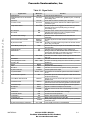
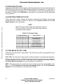

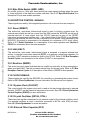
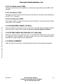
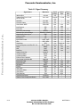

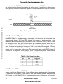

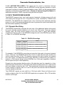


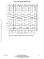
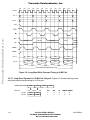
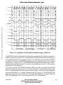


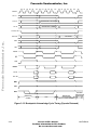
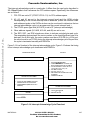


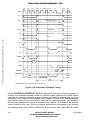

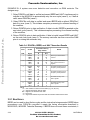


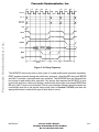
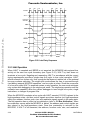
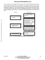

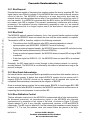
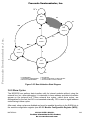
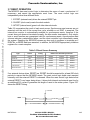
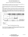


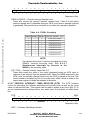


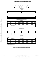

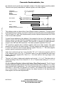
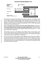


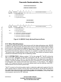


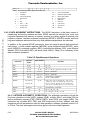


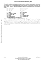
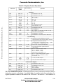


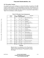
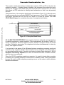
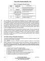


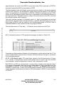

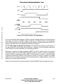

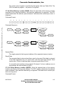
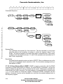

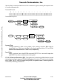


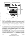
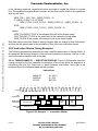
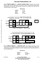


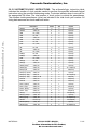


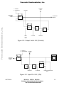

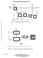


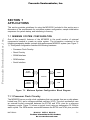

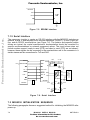
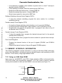

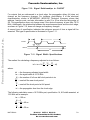
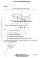


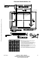
![CPU32 Reference Manual [330 pages!]](http://vs1.manualzilla.com/store/data/005686632_1-79fc9549061344d5fca8ab86e2038cb9-150x150.png)