1
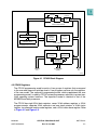
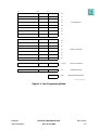
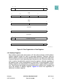
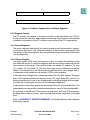
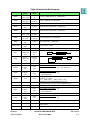
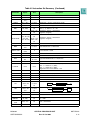
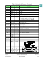
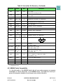
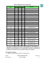
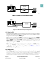
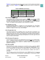
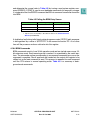
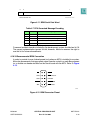
SECTION 4
CENTRAL PROCESSOR UNIT
The CPU32, the instruction processing module of the M68300 family, is based on the
industry-standard MC68000 processor. It has many features of the MC68010 and
MC68020, as well as unique features suited for high-performance controller applications. This section is an overview of the CPU32. For detailed information concerning
CPU operation, refer to the CPU32 Reference Manual (CPU32RM/AD).
4.1 General
Ease of programming is an important consideration in using a microcontroller. The
CPU32 instruction format reflects a philosophy emphasizing register-memory interaction. There are eight multifunction data registers and seven general-purpose
addressing registers.
All data resources are available to all operations requiring those resources. The data
registers readily support 8-bit (byte), 16-bit (word), and 32-bit (long-word) operand
lengths for all operations. Word and long-word operations support address manipulation. Although the program counter (PC) and stack pointers (SP) are special-purpose
registers, they are also available for most data addressing activities. Ease of program
checking and diagnosis is further enhanced by trace and trap capabilities at the
instruction level.
A block diagram of the CPU32 is shown in Figure 4-1. The major blocks operate in a
highly independent fashion that maximizes concurrency of operation while managing
the essential synchronization of instruction execution and bus operation. The bus controller loads instructions from the data bus into the decode unit. The sequencer and
control unit provide overall chip control, managing the internal buses, registers, and
functions of the execution unit.
MC68332
USER’S MANUAL
CENTRAL PROCESSOR UNIT
Rev. 15 Oct 2000
MOTOROLA
4-1
DECODE
BUFFER
STAGE
C
STAGE
B
STAGE
A
INSTRUCTION PIPELINE
CONTROL STORE
PROGRAM
COUNTER
SECTION
DATA
SECTION
CONTROL LOGIC
EXECUTION UNIT
MICROSEQUENCER AND CONTROL
WRITE PENDING
BUFFER
PREFETCH
CONTROLLER
MICROBUS
CONTROLLER
ADDRESS
BUS
BUS CONTROL
SIGNALS
DATA
BUS
1127A
Figure 4-1 CPU32 Block Diagram
4.2 CPU32 Registers
The CPU32 programming model consists of two groups of registers that correspond
to the user and supervisor privilege levels. User programs can use only the registers
of the user model. The supervisor programming model, which supplements the user
programming model, is used by CPU32 system programmers who wish to protect sensitive operating system functions. The supervisor model is identical to that of the
MC68010 and later processors.
The CPU32 has eight 32-bit data registers, seven 32-bit address registers, a 32-bit
program counter, separate 32-bit supervisor and user stack pointers, a 16-bit status
register, two alternate function code registers, and a 32-bit vector base register. Refer
to Figure 4-2 and Figure 4-3.
MC68332
USER’S MANUAL
CENTRAL PROCESSOR UNIT
Rev. 15 Oct 2000
MOTOROLA
4-2
31
16 15
8 7
0
D0
D1
D2
D3
DATA REGISTERS
D4
D5
D6
D7
31
16 15
0
A0
A1
A2
A3
ADDRESS REGISTERS
A4
A5
A6
31
16 15
0
A7 (SSP)
31
USER STACK POINTER
0
PC
7
PROGRAM COUNTER
0
CCR
CONDITION CODE REGISTER
CPU32 USER PROG MODEL
Figure 4-2 User Programming Model
MC68332
USER’S MANUAL
CENTRAL PROCESSOR UNIT
Rev. 15 Oct 2000
MOTOROLA
4-3
31
16 15
15
0
8 7
A7’ (SSP)
SUPERVISOR STACK POINTER
SR
STATUS REGISTER
VBR
VECTOR BASE REGISTER
SFC
ALTERNATE FUNCTION
DFC
CODE REGISTERS
0
(CCR)
31
0
2
0
CPU32 SUPV PROG MODEL
Figure 4-3 Supervisor Programming Model Supplement
4.2.1 Data Registers
The eight data registers can store data operands of 1, 8, 16, 32, and 64 bits and
addresses of 16 or 32 bits. The following data types are supported:
• Bits
• Packed Binary-Coded Decimal Digits
• Byte Integers (8 bits)
• Word Integers (16 bits)
• Long-Word Integers (32 bits)
• Quad-Word Integers (64 bits)
Each of data registers D7–D0 is 32 bits wide. Byte operands occupy the low-order 8
bits; word operands, the low-order 16 bits; and long-word operands, the entire 32 bits.
When a data register is used as either a source or destination operand, only the appropriate low-order byte or word (in byte or word operations, respectively) is used or
changed; the remaining high-order portion is unaffected. The least significant bit (LSB)
of a long-word integer is addressed as bit zero, and the most significant bit (MSB) is
addressed as bit 31. Figure 4-4 shows the organization of various types of data in the
data registers.
Quad-word data consists of two long words and represents the product of 32-bit multiply or the dividend of 32-bit divide operations (signed and unsigned). Quad-words
may be organized in any two data registers without restrictions on order or pairing.
There are no explicit instructions for the management of this data type, although the
MOVEM instruction can be used to move a quad-word into or out of the registers.
Binary-coded decimal (BCD) data represents decimal numbers in binary form. CPU32
BCD instructions use a format in which a byte contains two digits. The four LSB contain the least significant digit, and the four MSB contain the most significant digit. The
ABCD, SBCD, and NBCD instructions operate on two BCD digits packed into a single
byte.
MC68332
USER’S MANUAL
CENTRAL PROCESSOR UNIT
Rev. 15 Oct 2000
MOTOROLA
4-4
31
1
30
MSB
0
LSB
BYTE
31
24 23
HIGH-ORDER BYTE
16 15
MIDDLE HIGH BYTE
87
MIDDLE LOW BYTE
0
LOW-ORDER BYTE
WORD
31
16 15
HIGH-ORDER WORD
0
LOW-ORDER WORD
LONG WORD
31
0
LONG WORD
QUAD-WORD
63
62
MSB
32
HIGH-ORDER LONG WORD
1
31
LOW-ORDER LONG WORD
0
LSB
CPU32 DATA ORG
Figure 4-4 Data Organization in Data Registers
4.2.2 Address Registers
Each address register and stack pointer is 32 bits wide and holds a 32-bit address.
Address registers cannot be used for byte-sized operands. Therefore, when an
address register is used as a source operand, either the low-order word or the entire
long-word operand is used, depending upon the operation size. When an address register is used as the destination operand, the entire register is affected, regardless of
the operation size. If the source operand is a word size, it is sign-extended to 32 bits.
Address registers are used primarily for addresses and to support address computation. The instruction set includes instructions that add to, subtract from, compare, and
move the contents of address registers. Figure 4-5 shows the organization of
addresses in address registers.
MC68332
USER’S MANUAL
CENTRAL PROCESSOR UNIT
Rev. 15 Oct 2000
MOTOROLA
4-5
31
16 15
SIGN EXTENDED
0
16-BIT ADDRESS OPERAND
31
0
FULL 32-BIT ADDRESS OPERAND
CPU32 ADDR ORG
Figure 4-5 Address Organization in Address Registers
4.2.3 Program Counter
The PC contains the address of the next instruction to be executed by the CPU32.
During instruction execution and exception processing, the processor automatically
increments the contents of the PC or places a new value in the PC as appropriate.
4.2.4 Control Registers
The control registers described in this section contain control information for supervisor functions and vary in size. With the exception of the condition code register (the
user portion of the status register), they are accessed only by instructions at the supervisor privilege level.
4.2.4.1 Status Register
The status register (SR) stores the processor status. It contains the condition codes
that reflect the results of a previous operation and can be used for conditional instruction execution in a program. The condition codes are extend (X), negative (N), zero
(Z), overflow (V), and carry (C). The user (low-order) byte containing the condition
codes is the only portion of the SR information available at the user privilege level; it
is referenced as the condition code register (CCR) in user programs.
At the supervisor privilege level, software can access the full status register. The upper
byte of this register includes the interrupt priority (IP) mask (three bits), two bits for
placing the processor in one of two tracing modes or disabling tracing, and the supervisor/user bit for placing the processor at the desired privilege level.
Undefined bits in the status register are reserved by Motorola for future definition. The
undefined bits are read as zeros and should be written as zeros for future compatibility.
All operations to the SR and CCR are word-size operations, but for all CCR operations,
the upper byte is read as all zeros and is ignored when written, regardless of privilege
level.
Refer to APPENDIX D REGISTER SUMMARY for bit/field definitions and a diagram
of the status register.
MC68332
USER’S MANUAL
CENTRAL PROCESSOR UNIT
Rev. 15 Oct 2000
MOTOROLA
4-6
4.2.4.2 Alternate Function Code Registers
Alternate function code registers (SFC and DFC) contain 3-bit function codes. Function codes can be considered extensions of the 24-bit linear address that optionally
provide as many as eight 16-Mbyte address spaces. The processor automatically generates function codes to select address spaces for data and programs at the user and
supervisor privilege levels and to select a CPU address space used for processor
functions (such as breakpoint and interrupt acknowledge cycles).
Registers SFC and DFC are used by the MOVES instruction to specify explicitly the
function codes of the memory address. The MOVEC instruction is used to transfer values to and from the alternate function code registers. This is a long-word transfer; the
upper 29 bits are read as zeros and are ignored when written.
4.2.5 Vector Base Register (VBR)
The VBR contains the base address of the 1024-byte exception vector table, consisting of 256 exception vectors. Exception vectors contain the memory addresses of
routines that begin execution at the completion of exception processing. More
information on the VBR and exception processing can be found in 4.9 Exception
Processing.
4.3 Memory Organization
Memory is organized on a byte-addressable basis in which lower addresses correspond to higher order bytes. For example, the address N of a long-word data item
corresponds to the address of the most significant byte of the highest order word. The
address of the most significant byte of the low-order word is N + 2, and the address of
the least significant byte of the long word is N + 3. The CPU32 requires long-word and
word data and all instructions to be aligned on word boundaries. Refer to Figure 4-6.
If this does not happen, an exception will occur when the CPU32 accesses the
misaligned instruction or data. Data misalignment is not supported.
MC68332
USER’S MANUAL
CENTRAL PROCESSOR UNIT
Rev. 15 Oct 2000
MOTOROLA
4-7
BIT DATA
1 BYTE = 8 BITS
7
6
5
4
3
2
1
0
1 BYTE = 8 BITS
15
8 7
MSB
BYTE 0
0
LSB
BYTE 1
BYTE 2
BYTE 3
WORD = 16 BITS
15
0
WORD
0
WORD 0
MSB
LSB
WORD 1
WORD 2
LONG WORD = 32 BITS
0
15
MSB
HIGH ORDER
LONG WORD 0
LSB
LOW ORDER
LONG WORD 1
LONG WORD 2
ADDRESS 1
ADDRESS = 32 BITS
15
0
MSB
HIGH ORDER
ADDRESS 0
LOW ORDER
LSB
ADDRESS 1
ADDRESS 2
MSB = Most Significant Bit
LSB = Least Significant Bit
DECIMAL DATA
15
MSD
12 11
BCD DIGITS = 1 BYTE
8 7
BCD 0
BCD 1
BCD 4
BCD 5
LSD
4 3
0
BCD 2
BCD 3
BCD 6
BCD 7
MSD = Most Significant Digit
LSD = Least Significant Digit
1125A
Figure 4-6 Memory Operand Addressing
MC68332
USER’S MANUAL
CENTRAL PROCESSOR UNIT
Rev. 15 Oct 2000
MOTOROLA
4-8
4.4 Virtual Memory
The full addressing range of the CPU32 on the MC68332 is 16 Mbytes in each of eight
address spaces. Even though most systems implement a smaller physical memory,
the system can be made to appear to have a full 16 Mbytes of memory available to
each user program by using virtual memory techniques.
A system that supports virtual memory has a limited amount of high-speed physical
memory that can be accessed directly by the processor and maintains an image of a
much larger virtual memory on a secondary storage device. When the processor
attempts to access a location in the virtual memory map that is not resident in physical
memory, a page fault occurs. The access to that location is temporarily suspended
while the necessary data is fetched from secondary storage and placed in physical
memory. The suspended access is then restarted or continued.
The CPU32 uses instruction restart, which requires that only a small portion of the
internal machine state be saved. After correcting the fault, the machine state is
restored, and the instruction is fetched and started again. This process is completely
transparent to the application program.
4.5 Addressing Modes
Addressing in the CPU32 is register-oriented. Most instructions allow the results of the
specified operation to be placed either in a register or directly in memory. There is no
need for extra instructions to store register contents in memory.
There are seven basic addressing modes:
• Register Direct
• Register Indirect
• Register Indirect with Index
• Program Counter Indirect with Displacement
• Program Counter Indirect with Index
• Absolute
• Immediate
The register indirect addressing modes include postincrement, predecrement, and offset capability. The program counter indirect mode also has index and offset
capabilities. In addition to these addressing modes, many instructions implicitly specify
the use of the status register, stack pointer, and/or program counter.
4.6 Processing States
The processor is always in one of four processing states: normal, exception, halted, or
background. The normal processing state is associated with instruction execution; the
bus is used to fetch instructions and operands and to store results.
MC68332
USER’S MANUAL
CENTRAL PROCESSOR UNIT
Rev. 15 Oct 2000
MOTOROLA
4-9
The exception processing state is associated with interrupts, trap instructions, tracing,
and other exception conditions. The exception may be internally generated explicitly
by an instruction or by an unusual condition arising during the execution of an instruction. Exception processing can be forced externally by an interrupt, a bus error, or a
reset.
The halted processing state is an indication of catastrophic hardware failure. For
example, if during the exception processing of a bus error another bus error occurs,
the processor assumes that the system is unusable and halts.
The background processing state is initiated by breakpoints, execution of special
instructions, or a double bus fault. Background processing is enabled by pulling BKPT
low during RESET. Background processing allows interactive debugging of the system via a simple serial interface.
4.7 Privilege Levels
The processor operates at one of two levels of privilege: user or supervisor. Not all
instructions are permitted to execute at the user level, but all instructions are available
at the supervisor level. Effective use of privilege level can protect system resources
from uncontrolled access. The state of the S bit in the status register determines the
privilege level and whether the user stack pointer (USP) or supervisor stack pointer
(SSP) is used for stack operations.
4.8 Instructions
The CPU32 instruction set is summarized in Table 4-2. The instruction set of the
CPU32 is very similar to that of the MC68020. Two new instructions have been added
to facilitate controller applications: low-power stop (LPSTOP) and table lookup and
interpolate (TBLS, TBLSN, TBLU, TBLUN).
Table 4-1 shows the MC68020 instructions that are not implemented on the CPU32.
Table 4-1 Unimplemented MC68020 Instructions
BFxx
CALLM, RTM
CAS, CAS2
cpxxx
PACK, UNPK
Memory
— Bit Field Instructions (BFCHG, BFCLR, BFEXTS, BFEXTU, BFFFO, BFINS, BFSET, BFTST)
— Call Module, Return Module
— Compare and Swap (Read-Modify-Write Instructions)
— Coprocessor Instructions (cpBcc, cpDBcc, cpGEN)
— Pack, Unpack BCD Instructions
— Memory Indirect Addressing Modes
The CPU32 traps on unimplemented instructions or illegal effective addressing
modes, allowing user-supplied code to emulate unimplemented capabilities or to
define special purpose functions. However, Motorola reserves the right to use all currently unimplemented instruction operation codes for future M68000 core
enhancements.
MC68332
USER’S MANUAL
CENTRAL PROCESSOR UNIT
Rev. 15 Oct 2000
MOTOROLA
4-10
Table 4-2 Instruction Set Summary
Instruction
Operand
Syntax
Operand
Size
ABCD
Dn, Dn
− (An), − (An)
8
8
ADD
Dn, <ea>
<ea>, Dn
8, 16, 32
8, 16, 32
Source + Destination ⇒ Destination
ADDA
<ea>, An
16, 32
Source + Destination ⇒ Destination
ADDI
#<data>,
<ea>
8, 16, 32
Immediate data + Destination ⇒ Destination
ADDQ
# <data>,
<ea>
8, 16, 32
Immediate data + Destination ⇒ Destination
ADDX
Dn, Dn
− (An), − (An)
8, 16, 32
8, 16, 32
Source + Destination + X ⇒ Destination
AND
<ea>, Dn
Dn, <ea>
8, 16, 32
8, 16, 32
Source • Destination ⇒ Destination
ANDI
# <data>,
<ea>
8, 16, 32
Data • Destination ⇒ Destination
ANDI to CCR
# <data>,
CCR
8
Source • CCR ⇒ CCR
ANDI to SR1 1
# <data>, SR
16
Source • SR ⇒ SR
ASL
Dn, Dn
# <data>, Dn
<ea>
8, 16, 32
8, 16, 32
16
ASR
Dn, Dn
# <data>, Dn
<ea>
8, 16, 32
8, 16, 32
16
Bcc
label
8, 16, 32
BCHG
Dn, <ea>
# <data>,
<ea>
8, 32
8, 32
BCLR
Dn, <ea>
# <data>,
<ea>
8, 32
8, 32
( 〈 bit number〉 of destination ) ⇒ Z;
0 ⇒ bit of destination
BGND
none
none
If background mode enabled, then enter background mode, else format/vector ⇒ − (SSP);
PC ⇒ − (SSP); SR ⇒ − (SSP); (vector) ⇒ PC
BKPT
# <data>
none
If breakpoint cycle acknowledged, then execute
returned operation word, else trap as illegal instruction
BRA
label
8, 16, 32
BSET
Dn, <ea>
# <data>,
<ea>
8, 32
8, 32
BSR
label
8, 16, 32
BTST
Dn, <ea>
# <data>,
<ea>
8, 32
8, 32
CHK
<ea>, Dn
16, 32
Description
Source10 + Destination10 + X ⇒ Destination
X/C
X/C
If condition true, then PC + d ⇒ PC
( 〈 bit number〉 of destination ) ⇒ Z ⇒ bit of destination
PC + d ⇒ PC
( 〈 bit number 〉 of destination ) ⇒ Z;
1 ⇒ bit of destination
SP − 4 ⇒ SP; PC ⇒ (SP); PC + d ⇒ PC
( 〈 bit number〉 of destination ) ⇒ Z
If Dn < 0 or Dn > (ea), then CHK exception
CHK2
<ea>, Rn
8, 16, 32
If Rn < lower bound or Rn > upper bound, then
CHK exception
CLR
<ea>
8, 16, 32
0 ⇒ Destination
MC68332
USER’S MANUAL
0
CENTRAL PROCESSOR UNIT
Rev. 15 Oct 2000
MOTOROLA
4-11
Table 4-2 Instruction Set Summary (Continued)
Instruction
Operand
Syntax
Operand
Size
Description
CMP
<ea>, Dn
8, 16, 32
(Destination − Source), CCR shows results
CMPA
<ea>, An
16, 32
(Destination − Source), CCR shows results
CMPI
# <data>,
<ea>
8, 16, 32
(Destination − Data), CCR shows results
CMPM
(An) +, (An) +
8, 16, 32
(Destination − Source), CCR shows results
CMP2
<ea>, Rn
8, 16, 32
DBcc
Dn, label
DIVS/DIVU
<ea>, Dn
DIVSL/DIVUL
16
Lower bound ≤ Rn ≤ Upper bound, CCR shows result
If condition false, then Dn − 1 ⇒ PC;
if Dn ≠ (− 1), then PC + d ⇒ PC
32/16 ⇒ 16 : Destination / Source ⇒ Destination
16
(signed or unsigned)
64/32 ⇒ 32 :
32
<ea>, Dr : Dq
Destination / Source ⇒ Destination
32/32 ⇒ 32
<ea>, Dq
(signed or unsigned)
<ea>, Dr : Dq 32/32 ⇒ 32 :
32
EOR
Dn, <ea>
8, 16, 32
Source ⊕ Destination ⇒ Destination
EORI
# <data>,
<ea>
8, 16, 32
Data ⊕ Destination ⇒ Destination
EORI to CCR
# <data>,
CCR
8
Source ⊕ CCR ⇒ CCR
EORI to SR1
# <data>, SR
16
Source ⊕ SR ⇒ SR
EXG
Rn, Rn
32
Rn ⇒ Rn
EXT
Dn
Dn
8 ⇒ 16
16 ⇒ 32
Sign extended Destination ⇒ Destination
EXTB
Dn
8 ⇒ 32
Sign extended Destination ⇒ Destination
ILLEGAL
none
none
SSP − 2 ⇒ SSP; vector offset ⇒ (SSP);
SSP − 4 ⇒ SSP; PC ⇒ (SSP);
SSP − 2 ⇒ SSP; SR ⇒ (SSP);
Illegal instruction vector address ⇒ PC
JMP
<ea>
none
Destination ⇒ PC
JSR
<ea>
none
SP − 4 ⇒ SP; PC ⇒ (SP); destination ⇒ PC
LEA
<ea>, An
32
LINK
An, # d
16, 32
LPSTOP1
# <data>
16
LSL
Dn, Dn
# <data>, Dn
<ea>
8, 16, 32
8, 16, 32
16
LSR
Dn, Dn
#<data>, Dn
<ea>
8, 16, 32
8, 16, 32
16
MOVE
<ea>, <ea>
8, 16, 32
Source ⇒ Destination
MOVEA
<ea>, An
16, 32 ⇒ 32
Source ⇒ Destination
MOVEA1
USP, An
An, USP
32
32
USP ⇒ An
An ⇒ USP
MOVE from
CCR
CCR, <ea>
16
CCR ⇒ Destination
MOVE to CCR
<ea>, CCR
16
Source ⇒ CCR
MC68332
USER’S MANUAL
<ea> ⇒ An
SP − 4 ⇒ SP, An ⇒ (SP); SP ⇒ An, SP + d ⇒ SP
Data ⇒ SR; interrupt mask ⇒ EBI; STOP
X/C
0
CENTRAL PROCESSOR UNIT
Rev. 15 Oct 2000
0
X/C
MOTOROLA
4-12
Table 4-2 Instruction Set Summary (Continued)
Operand
Syntax
Operand
Size
SR1
SR, <ea>
16
SR ⇒ Destination
MOVE to SR1
<ea>, SR
16
Source ⇒ SR
MOVE USP1
USP, An
An, USP
32
32
USP ⇒ An
An ⇒ USP
MOVEC1
Rc, Rn
Rn, Rc
32
32
Rc ⇒ Rn
Rn ⇒ Rc
MOVEM
list, <ea>
<ea>, list
16, 32
16, 32 ⇒ 32
Instruction
MOVE from
Description
Listed registers ⇒ Destination
Source ⇒ Listed registers
Dn [31 : 24] ⇒ (An + d); Dn [23 : 16] ⇒ (An + d + 2);
Dn [15 : 8] ⇒ (An + d + 4); Dn [7 : 0] ⇒ (An + d + 6)
Dn, (d16, An)
16, 32
MOVEP
(An + d) ⇒ Dn [31 : 24]; (An + d + 2) ⇒ Dn [23 : 16];
(An + d + 4) ⇒ Dn [15 : 8]; (An + d + 6) ⇒ Dn [7 : 0]
(d16, An), Dn
8 ⇒ 32
Immediate data ⇒ Destination
MOVEQ
#<data>, Dn
MOVES1
Rn, <ea>
<ea>, Rn
MULS/MULU
<ea>, Dn
<ea>, Dl
<ea>, Dh : Dl
NBCD
<ea>
8
8
NEG
<ea>
8, 16, 32
0 − Destination ⇒ Destination
NEGX
<ea>
8, 16, 32
0 − Destination − X ⇒ Destination
8, 16, 32
Rn ⇒ Destination using DFC
Source using SFC ⇒ Rn
16 ∗ 16 ⇒ 32
Source ∗ Destination ⇒ Destination
32 ∗ 32 ⇒ 32
(signed or unsigned)
32 ∗ 32 ⇒ 64
0 − Destination 10 − X ⇒ Destination
PC + 2 ⇒ PC
NOP
none
none
NOT
<ea>
8, 16, 32
Destination ⇒ Destination
OR
<ea>, Dn
Dn, <ea>
8, 16, 32
8, 16, 32
Source + Destination ⇒ Destination
ORI
#<data>,
<ea>
8, 16, 32
Data + Destination ⇒ Destination
ORI to CCR
#<data>,
CCR
16
Source + CCR ⇒ SR
ORI to SR1
#<data>, SR
16
Source ; SR ⇒ SR
PEA
<ea>
32
SP − 4 ⇒ SP; <ea> ⇒ SP
RESET1
none
none
ROL
Dn, Dn
#<data>, Dn
<ea>
8, 16, 32
8, 16, 32
16
ROR
Dn, Dn
#<data>, Dn
<ea>
8, 16, 32
8, 16, 32
16
ROXL
Dn, Dn
#<data>, Dn
<ea>
8, 16, 32
8, 16, 32
16
ROXR
Dn, Dn
#<data>, Dn
<ea>
8, 16, 32
8, 16, 32
16
RTD
#d
16
MC68332
USER’S MANUAL
Assert RESET line
C
C
C
X
X
C
(SP) ⇒ PC; SP + 4 + d ⇒ SP
CENTRAL PROCESSOR UNIT
Rev. 15 Oct 2000
MOTOROLA
4-13
Table 4-2 Instruction Set Summary (Continued)
Instruction
Operand
Syntax
Operand
Size
RTE1
none
none
(SP) ⇒ SR; SP + 2 ⇒ SP; (SP) ⇒ PC;
SP + 4 ⇒ SP;
Restore stack according to format
RTR
none
none
(SP) ⇒ CCR; SP + 2 ⇒ SP; (SP) ⇒ PC;
SP + 4 ⇒ SP
RTS
none
none
(SP) ⇒ PC; SP + 4 ⇒ SP
SBCD
Dn, Dn
− (An), − (An)
8
8
Destination10 − Source10 − X ⇒ Destination
Scc
<ea>
8
If condition true, then destination bits are set to one;
else, destination bits are cleared to zero
STOP1
#<data>
16
Data ⇒ SR; STOP
SUB
<ea>, Dn
Dn, <ea>
8, 16, 32
Destination − Source ⇒ Destination
SUBA
<ea>, An
16, 32
Destination − Source ⇒ Destination
SUBI
#<data>,
<ea>
8, 16, 32
Destination − Data ⇒ Destination
SUBQ
#<data>,
<ea>
8, 16, 32
Destination − Data ⇒ Destination
SUBX
Dn, Dn
− (An), − (An)
8, 16, 32
8, 16, 32
Destination − Source − X ⇒ Destination
SWAP
Dn
16
TAS
<ea>
8
TBLS/TBLU
<ea>, Dn
Dym : Dyn,
Dn
8, 16, 32
Dyn − Dym ⇒ Temp
(Temp ∗ Dn [7 : 0]) ⇒ Temp
(Dym ∗ 256) + Temp ⇒ Dn
TBLSN/TBLUN
<ea>, Dn
Dym : Dyn,
Dn
8, 16, 32
Dyn − Dym ⇒ Temp
(Temp ∗ Dn [7 : 0]) / 256 ⇒ Temp
Dym + Temp ⇒ Dn
TRAP
#<data>
none
SSP − 2 ⇒ SSP; format/vector offset ⇒ (SSP);
SSP − 4 ⇒ SSP; PC ⇒ (SSP); SR ⇒ (SSP);
vector address ⇒ PC
TRAPcc
none
#<data>
none
16, 32
If cc true, then TRAP exception
TRAPV
none
none
TST
<ea>
8, 16, 32
UNLK
An
32
Description
MSW
LSW
Destination Tested Condition Codes bit 7 of
Destination
If V set, then overflow TRAP exception
Source − 0, to set condition codes
An ⇒ SP; (SP) ⇒ An, SP + 4 ⇒ SP
NOTES:
1. Privileged instruction.
4.8.1 M68000 Family Compatibility
It is the philosophy of the M68000 family that all user-mode programs can execute
unchanged on future derivatives of the M68000 family, and supervisor-mode programs and exception handlers should require only minimal alteration.
MC68332
USER’S MANUAL
CENTRAL PROCESSOR UNIT
Rev. 15 Oct 2000
MOTOROLA
4-14
The CPU32 can be thought of as an intermediate member of the M68000 Family.
Object code from an MC68000 or MC68010 may be executed on the CPU32. Many of
the instruction and addressing mode extensions of the MC68020 are also supported.
Refer to the CPU32 Reference Manual (CPU32RM/AD) for a detailed comparison of
the CPU32 and MC68020 instruction set.
4.8.2 Special Control Instructions
Low-power stop (LPSTOP) and table lookup and interpolate (TBL) instructions have
been added to the MC68000 instruction set for use in controller applications.
4.8.2.1 Low-Power Stop (LPSTOP)
In applications where power consumption is a consideration, the CPU32 forces the
device into a low-power standby mode when immediate processing is not required.
The low-power stop mode is entered by executing the LPSTOP instruction. The processor remains in this mode until a user-specified (or higher) interrupt level or reset
occurs.
4.8.2.2 Table Lookup and Interpolate (TBL)
To maximize throughput for real-time applications, reference data is often precalculated and stored in memory for quick access. Storage of many data points can require
an inordinate amount of memory. The table lookup instruction requires that only a
sample of data points be stored, reducing memory requirements. The TBL instruction
recovers intermediate values using linear interpolation. Results can be rounded with a
round-to-nearest algorithm.
4.8.2.3 Loop Mode Instruction Execution
The CPU32 has several features that provide efficient execution of program loops.
One of these features is the DBcc looping primitive instruction. To increase the performance of the CPU32, a loop mode has been added to the processor. The loop mode
is used by any single word instruction that does not change the program flow. Loop
mode is implemented in conjunction with the DBcc instruction. Figure 4-7 shows the
required form of an instruction loop for the processor to enter loop mode.
ONE WORD INSTRUCTION
DBCC
DBCC DISPLACEMENT
$FFFC = – 4
1126A
Figure 4-7 Loop Mode Instruction Sequence
MC68332
USER’S MANUAL
CENTRAL PROCESSOR UNIT
Rev. 15 Oct 2000
MOTOROLA
4-15
The loop mode is entered when the DBcc instruction is executed, and the loop displacement is –4. Once in loop mode, the processor performs only the data cycles
associated with the instruction and suppresses all instruction fetches. The termination
condition and count are checked after each execution of the data operations of the
looped instruction. The CPU32 automatically exits the loop mode on interrupts or other
exceptions. All single word instructions that do not cause a change of flow can be
looped.
4.9 Exception Processing
An exception is a special condition that preempts normal processing. Exception processing is the transition from normal mode program execution to execution of a routine
that deals with an exception.
4.9.1 Exception Vectors
An exception vector is the address of a routine that handles an exception. The vector
base register (VBR) contains the base address of a 1024-byte exception vector table,
which consists of 256 exception vectors. Sixty-four vectors are defined by the
processor, and 192 vectors are reserved for user definition as interrupt vectors. Except
for the reset vector, each vector in the table is one long word in length. The reset vector
is two long words in length. Refer to Table 4-3 for information on vector assignment.
CAUTION
Because there is no protection on the 64 processor-defined vectors,
external devices can access vectors reserved for internal purposes.
This practice is strongly discouraged.
All exception vectors, except the reset vector and stack pointer, are located in supervisor data space. The reset vector and stack pointer are located in supervisor program
space. Only the initial reset vector and stack pointer are fixed in the processor memory
map. When initialization is complete, there are no fixed assignments. Since the VBR
stores the vector table base address, the table can be located anywhere in memory.
It can also be dynamically relocated for each task executed by an operating system.
MC68332
USER’S MANUAL
CENTRAL PROCESSOR UNIT
Rev. 15 Oct 2000
MOTOROLA
4-16
Table 4-3 Exception Vector Assignments
Vector Offset
Vector
Number
Dec
Hex
Space
0
0
000
SP
Reset: initial stack pointer
1
4
004
SP
Reset: initial program counter
Assignment
2
8
008
SD
Bus error
3
12
00C
SD
Address error
4
16
010
SD
Illegal instruction
5
20
014
SD
Zero division
6
24
018
SD
CHK, CHK2 instructions
7
28
01C
SD
TRAPcc, TRAPV instructions
8
32
020
SD
Privilege violation
9
36
024
SD
Trace
10
40
028
SD
Line 1010 emulator
11
44
02C
SD
Line 1111 emulator
12
48
030
SD
Hardware breakpoint
13
52
034
SD
(Reserved, coprocessor protocol violation)
14
56
038
SD
Format error and uninitialized interrupt
15
60
03C
SD
Format error and uninitialized interrupt
16–23
64
92
040
05C
SD
(Unassigned, reserved)
24
96
060
SD
Spurious interrupt
25
100
064
SD
Level 1 interrupt autovector
26
104
068
SD
Level 2 interrupt autovector
27
108
06C
SD
Level 3 interrupt autovector
28
112
070
SD
Level 4 interrupt autovector
29
116
074
SD
Level 5 interrupt autovector
30
120
078
SD
Level 6 interrupt autovector
31
124
07C
SD
Level 7 interrupt autovector
32–47
128
188
080
0BC
SD
Trap instruction vectors (0–15)
48–58
192
232
0C0
0E8
SD
(Reserved, coprocessor)
59–63
236
252
0EC
0FC
SD
(Unassigned, reserved)
64–255
256
1020
100
3FC
SD
User defined vectors (192)
Each vector is assigned an 8-bit number. Vector numbers for some exceptions are
obtained from an external device; others are supplied by the processor. The processor
multiplies the vector number by four to calculate vector offset, then adds the offset to
the contents of the VBR. The sum is the memory address of the vector.
4.9.2 Types of Exceptions
An exception can be caused by internal or external events.
MC68332
USER’S MANUAL
CENTRAL PROCESSOR UNIT
Rev. 15 Oct 2000
MOTOROLA
4-17
An internal exception can be generated by an instruction or by an error. The TRAP,
TRAPcc, TRAPV, BKPT, CHK, CHK2, RTE, and DIV instructions can cause exceptions during normal execution. Illegal instructions, instruction fetches from odd
addresses, word or long-word operand accesses from odd addresses, and privilege
violations also cause internal exceptions.
Sources of external exception include interrupts, breakpoints, bus errors, and reset
requests. Interrupts are peripheral device requests for processor action. Breakpoints
are used to support development equipment. Bus error and reset are used for access
control and processor restart.
4.9.3 Exception Processing Sequence
For all exceptions other than a reset exception, exception processing occurs in the following sequence. Refer to 5.7 Reset for details of reset processing.
As exception processing begins, the processor makes an internal copy of the status
register. After the copy is made, the processor state bits in the status register are
changed — the S bit is set, establishing supervisor access level, and bits T1 and T0
are cleared, disabling tracing. For reset and interrupt exceptions, the interrupt priority
mask is also updated.
Next, the exception number is obtained. For interrupts, the number is fetched from
CPU space $F (the bus cycle is an interrupt acknowledge). For all other exceptions,
internal logic provides a vector number.
Next, current processor status is saved. An exception stack frame is created and
placed on the supervisor stack. All stack frames contain copies of the status register
and the program counter for use by RTE. The type of exception and the context in
which the exception occurs determine what other information is stored in the stack
frame.
Finally, the processor prepares to resume normal execution of instructions. The
exception vector offset is determined by multiplying the vector number by four, and the
offset is added to the contents of the VBR to determine displacement into the exception vector table. The exception vector is loaded into the program counter. If no other
exception is pending, the processor will resume normal execution at the new address
in the PC.
4.10 Development Support
The following features have been implemented on the CPU32 to enhance the instrumentation and development environment:
• M68000 Family Development Support
• Background Debug Mode
• Deterministic Opcode Tracking
• Hardware Breakpoints
MC68332
USER’S MANUAL
CENTRAL PROCESSOR UNIT
Rev. 15 Oct 2000
MOTOROLA
4-18
4.10.1 M68000 Family Development Support
All M68000 Family members include features to facilitate applications development.
These features include the following:
Trace on Instruction Execution — M68000 Family processors include an instructionby-instruction tracing facility as an aid to program development. The MC68020,
MC68030, MC68040, and CPU32 also allow tracing only of those instructions causing
a change in program flow. In the trace mode, a trace exception is generated after an
instruction is executed, allowing a debugger program to monitor the execution of a program under test.
Breakpoint Instruction — An emulator may insert software breakpoints into the target
code to indicate when a breakpoint has occurred. On the MC68010, MC68020,
MC68030, and CPU32, this function is provided via illegal instructions, $4848–$484F,
to serve as breakpoint instructions.
Unimplemented Instruction Emulation — During instruction execution, when an
attempt is made to execute an illegal instruction, an illegal instruction exception
occurs. Unimplemented instructions (F-line, A-line, . . .) utilize separate exception vectors to permit efficient emulation of unimplemented instructions in software.
4.10.2 Background Debug Mode
Microcomputer systems generally provide a debugger, implemented in software, for
system analysis at the lowest level. The background debug mode (BDM) on the
CPU32 is unique in that the debugger has been implemented in CPU microcode.
BDM incorporates a full set of debugging options: registers can be viewed or altered,
memory can be read or written to, and test features can be invoked.
A resident debugger simplifies implementation of an in-circuit emulator. In a common
setup (refer to Figure 4-8), emulator hardware replaces the target system processor.
A complex, expensive pod-and-cable interface provides a communication path
between the target system and the emulator.
By contrast, an integrated debugger supports use of a bus state analyzer (BSA) for incircuit emulation. The processor remains in the target system (refer to Figure 4-9) and
the interface is simplified. The BSA monitors target processor operation and the onchip debugger controls the operating environment. Emulation is much “closer” to target hardware, and many interfacing problems (for example, limitations on highfrequency operation, AC and DC parametric mismatches, and restrictions on cable
length) are minimized.
MC68332
USER’S MANUAL
CENTRAL PROCESSOR UNIT
Rev. 15 Oct 2000
MOTOROLA
4-19
TARGET
SYSTEM
IN-CIRCUIT
EMULATOR
TARGET
MCU
1128A
Figure 4-8 Common In-Circuit Emulator Diagram
TARGET
SYSTEM
BUS STATE
ANALYZER
TARGET
MCU
1129A
Figure 4-9 Bus State Analyzer Configuration
4.10.3 Enabling BDM
Accidentally entering BDM in a non-development environment can lock up the CPU32
when the serial command interface is not available. For this reason, BDM is enabled
during reset via the breakpoint (BKPT) signal.
BDM operation is enabled when BKPT is asserted (low), at the rising edge of RESET.
BDM remains enabled until the next system reset. A high BKPT signal on the trailing
edge of RESET disables BDM. BKPT is latched again on each rising transition of
RESET. BKPT is synchronized internally, and must be held low for at least two clock
cycles prior to negation of RESET.
BDM enable logic must be designed with special care. If hold time on BKPT (after the
trailing edge of RESET) extends into the first bus cycle following reset, the bus cycle
could inadvertently be tagged with a breakpoint. Refer to the SIM Reference Manual
(SIMRM/AD) for timing information.
4.10.4 BDM Sources
When BDM is enabled, any of several sources can cause the transition from normal
mode to BDM. These sources include external breakpoint hardware, the BGND
instruction, a double bus fault, and internal peripheral breakpoints. If BDM is not
enabled when an exception condition occurs, the exception is processed normally.
MC68332
USER’S MANUAL
CENTRAL PROCESSOR UNIT
Rev. 15 Oct 2000
MOTOROLA
4-20
Table 4-4 summarizes the processing of each source for both enabled and disabled
cases. As shown in Table 4-4, the BKPT instruction never causes a transition into
BDM.
Table 4-4 BDM Source Summary
Source
BDM Enabled
BDM Disabled
BKPT
Background
Breakpoint Exception
Double Bus Fault
Background
Halted
BGND Instruction
Background
Illegal Instruction
BKPT Instruction
Opcode Substitution/
Illegal Instruction
Opcode Substitution/
Illegal Instruction
4.10.4.1 External BKPT Signal
Once enabled, BDM is initiated whenever assertion of BKPT is acknowledged. If BDM
is disabled, a breakpoint exception (vector $0C) is acknowledged. The BKPT input has
the same timing relationship to the data strobe trailing edge as does read cycle data.
There is no breakpoint acknowledge bus cycle when BDM is entered.
4.10.4.2 BGND Instruction
An illegal instruction, $4AFA, is reserved for use by development tools. The CPU32
defines $4AFA (BGND) to be a BDM entry point when BDM is enabled. If BDM is
disabled, an illegal instruction trap is acknowledged.
4.10.4.3 Double Bus Fault
The CPU32 normally treats a double bus fault, or two bus faults in succession, as a
catastrophic system error, and halts. When this condition occurs during initial system
debug (a fault in the reset logic), further debugging is impossible until the problem is
corrected. In BDM, the fault can be temporarily bypassed, so that the origin of the fault
can be isolated and eliminated.
4.10.4.4 Peripheral Breakpoints
CPU32 peripheral breakpoints are implemented in the same way as external breakpoints — peripherals request breakpoints by asserting the BKPT signal. Consult the
appropriate peripheral user’s manual for additional details on the generation of
peripheral breakpoints.
4.10.5 Entering BDM
When the processor detects a breakpoint or a double bus fault, or decodes a BGND
instruction, it suspends instruction execution and asserts the FREEZE output. This is
the first indication that the processor has entered BDM. Once FREEZE has been
asserted, the CPU enables the serial communication hardware and awaits a
command.
The CPU writes a unique value indicating the source of BDM transition into temporary
register A (ATEMP) as part of the process of entering BDM. A user can poll ATEMP
MC68332
USER’S MANUAL
CENTRAL PROCESSOR UNIT
Rev. 15 Oct 2000
MOTOROLA
4-21
and determine the source (refer to Table 4-5) by issuing a read system register command (RSREG). ATEMP is used in most debugger commands for temporary storage.
It is imperative that the RSREG command be the first command issued after transition
into BDM.
Table 4-5 Polling the BDM Entry Source
Source
ATEMP[31:16]
ATEMP[15:0]
Double Bus Fault
SSW1
$FFFF
BGND Instruction
$0000
$0001
Hardware Breakpoint
$0000
$0000
NOTES:
1. Special status word (SSW) is described in detail in the CPU32 Reference
Manual (CPU32RM/AD).
A double bus fault during initial stack pointer/program counter (SP/PC) fetch sequence
is distinguished by a value of $FFFFFFFF in the current instruction PC. At no other
time will the processor write an odd value into this register.
4.10.6 BDM Commands
BDM commands consist of one 16-bit operation word and can include one or more 16bit extension words. Each incoming word is read as it is assembled by the serial interface. The microcode routine corresponding to a command is executed as soon as the
command is complete. Result operands are loaded into the output shift register to be
shifted out as the next command is read. This process is repeated for each command
until the CPU returns to normal operating mode. Table 4-6 is a summary of background mode commands.
MC68332
USER’S MANUAL
CENTRAL PROCESSOR UNIT
Rev. 15 Oct 2000
MOTOROLA
4-22
Table 4-6 Background Mode Command Summary
Command
Mnemonic
Description
Read D/A Register
RDREG/RAREG
Read the selected address or data register and return the
results via the serial interface.
Write D/A Register
WDREG/WAREG
The data operand is written to the specified address or data
register.
Read System Register
RSREG
The specified system control register is read. All registers that
can be read in supervisor mode can be read in background
mode.
Write System Register
WSREG
The operand data is written into the specified system control
register.
Read Memory Location
READ
Read the sized data at the memory location specified by the
long-word address. The source function code register (SFC)
determines the address space accessed.
Write Memory Location
WRITE
Write the operand data to the memory location specified by the
long-word address. The destination function code (DFC) register determines the address space accessed.
DUMP
Used in conjunction with the READ command to dump large
blocks of memory. An initial READ is executed to set up the
starting address of the block and retrieve the first result. Subsequent operands are retrieved with the DUMP command.
Fill Memory Block
FILL
Used in conjunction with the WRITE command to fill large
blocks of memory. An initial WRITE is executed to set up the
starting address of the block and supply the first operand. Subsequent operands are written with the FILL command.
Resume Execution
GO
The pipe is flushed and re-filled before resuming instruction
execution at the current PC.
Patch User Code
CALL
Current program counter is stacked at the location of the current stack pointer. Instruction execution begins at user patch
code.
Reset Peripherals
RST
Asserts RESET for 512 clock cycles. The CPU is not reset by
this command. Synonymous with the CPU RESET instruction.
No Operation
NOP
NOP performs no operation and may be used as a null command.
Dump Memory Block
4.10.7 Background Mode Registers
BDM processing uses three special purpose registers to keep track of program context
during development. A description of each follows.
4.10.7.1 Fault Address Register (FAR)
The FAR contains the address of the faulting bus cycle immediately following a bus or
address error. This address remains available until overwritten by a subsequent bus
cycle. Following a double bus fault, the FAR contains the address of the last bus cycle.
The address of the first fault (if there was one) is not visible to the user.
4.10.7.2 Return Program Counter (RPC)
The RPC points to the location where fetching will commence after transition from
background mode to normal mode. This register should be accessed to change the
MC68332
USER’S MANUAL
CENTRAL PROCESSOR UNIT
Rev. 15 Oct 2000
MOTOROLA
4-23
flow of a program under development. Changing the RPC to an odd value will cause
an address error when normal mode prefetching begins.
4.10.7.3 Current Instruction Program Counter (PCC)
The PCC holds a pointer to the first word of the last instruction executed prior to transition into background mode. Due to instruction pipelining, the instruction pointed to
may not be the instruction which caused the transition. An example is a breakpoint on
a released write. The bus cycle may overlap as many as two subsequent instructions
before stalling the instruction sequencer. A breakpoint asserted during this cycle will
not be acknowledged until the end of the instruction executing at completion of the bus
cycle. PCC will contain $00000001 if BDM is entered via a double bus fault immediately out of reset.
4.10.8 Returning from BDM
BDM is terminated when a resume execution (GO) or call user code (CALL) command
is received. Both GO and CALL flush the instruction pipeline and refetch instructions
from the location pointed to by the RPC.
The return PC and the memory space referred to by the status register SUPV bit reflect
any changes made during BDM. FREEZE is negated prior to initiating the first prefetch. Upon negation of FREEZE, the serial subsystem is disabled, and the signals
revert to IPIPE/IFETCH functionality.
4.10.9 Serial Interface
Communication with the CPU32 during BDM occurs via a dedicated serial interface,
which shares pins with other development features. Figure 4-10 is a block diagram of
the interface. The BKPT signal becomes the serial clock (DSCLK); serial input data
(DSI) is received on IFETCH, and serial output data (DSO) is transmitted on IPIPE.
MC68332
USER’S MANUAL
CENTRAL PROCESSOR UNIT
Rev. 15 Oct 2000
MOTOROLA
4-24
CPU
DEVELOPMENT SYSTEM
INSTRUCTION
REGISTER BUS
DATA
16
16
0
RCV DATA LATCH
COMMAND LATCH
DSI
SERIAL IN
PARALLEL OUT
PARALLEL IN
SERIAL OUT
DSO
SERIAL IN
PARALLEL OUT
PARALLEL IN
SERIAL OUT
16
STATUS
RESULT LATCH
EXECUTION
UNIT
16
SYNCHRONIZE
MICROSEQUENCER
STATUS
M
CONTROL
LOGIC
DSCLK
DATA
CONTROL
LOGIC
SERIAL
CLOCK
32 DEBUG I/O BLOCK
Figure 4-10 Debug Serial I/O Block Diagram
The serial interface uses a full-duplex synchronous protocol similar to the serial peripheral interface (SPI) protocol. The development system serves as the master of the
serial link since it is responsible for the generation of DSCLK. If DSCLK is derived from
the CPU32 system clock, development system serial logic is unhindered by the operating frequency of the target processor. Operable frequency range of the serial clock
is from DC to one-half the processor system clock frequency.
The serial interface operates in full-duplex mode — data is transmitted and received
simultaneously by both master and slave devices. In general, data transitions occur on
the falling edge of DSCLK and are stable by the following rising edge of DSCLK. Data
is transmitted MSB first, and is latched on the rising edge of DSCLK.
The serial data word is 17 bits wide, including 16 data bits and a status/control bit (refer
to Figure 4-11). Bit 16 indicates the status of CPU-generated messages. Table 4-7
shows the CPU-generated message types.
MC68332
USER’S MANUAL
CENTRAL PROCESSOR UNIT
Rev. 15 Oct 2000
MOTOROLA
4-25
16
0
15
DATA FIELD
S/C
⇑
STATUS CONTROL BIT
BDM SERIAL DATA WORD
Figure 4-11 BDM Serial Data Word
Table 4-7 CPU Generated Message Encoding
Bit 16
Data
0
XXXX
Valid data transfer
Message Type
0
FFFF
Command complete; Status OK
1
0000
Not ready with response; Come again
1
0001
BERR terminated bus cycle; Data invalid
1
FFFF
Illegal command
Command and data transfers initiated by the development system should clear bit 16.
The current implementation ignores this bit; however, Motorola reserves the right to
use this bit for future enhancements.
4.10.10 Recommended BDM Connection
In order to provide for use of development tools when an MCU is installed in a system,
Motorola recommends that appropriate signal lines be routed to a male Berg connector or double-row header installed on the circuit board with the MCU. Refer to Figure
4-12.
1
2
BERR
GND 3
4
BKPT/DSCLK
GND 5
6
FREEZE
RESET 7
8
IFETCH/DSI
VDD 9
10
IPIPE/DSO
DS
32 BERG
Figure 4-12 BDM Connector Pinout
MC68332
USER’S MANUAL
CENTRAL PROCESSOR UNIT
Rev. 15 Oct 2000
MOTOROLA
4-26
4.10.11 Deterministic Opcode Tracking
CPU32 function code outputs are augmented by two supplementary signals to monitor
the instruction pipeline. The instruction pipe (IPIPE) output indicates the start of each
new instruction and each mid-instruction pipeline advance. The instruction fetch
(IFETCH) output identifies the bus cycles in which the operand is loaded into the
instruction pipeline. Pipeline flushes are also signaled with IFETCH. Monitoring these
two signals allows a bus state analyzer to synchronize itself to the instruction stream
and monitor its activity.
4.10.12 On-Chip Breakpoint Hardware
An external breakpoint input and on-chip breakpoint hardware allow a breakpoint trap
on any memory access. Off-chip address comparators preclude breakpoints unless
show cycles are enabled. Breakpoints on instruction prefetches that are ultimately
flushed from the instruction pipeline are not acknowledged; operand breakpoints are
always acknowledged. Acknowledged breakpoints initiate exception processing at the
address in exception vector number 12, or alternately enter background mode.
MC68332
USER’S MANUAL
CENTRAL PROCESSOR UNIT
Rev. 15 Oct 2000
MOTOROLA
4-27
MC68332
USER’S MANUAL
CENTRAL PROCESSOR UNIT
Rev. 15 Oct 2000
MOTOROLA
4-28

![CPU32 Reference Manual [330 pages!]](http://vs1.manualzilla.com/store/data/005686632_1-79fc9549061344d5fca8ab86e2038cb9-150x150.png)