1
F&eIT Series
Isolated RS-422A/485 1ch
Communication Module
COM-1PD(FIT)GY
User’s Manual
CONTEC CO.,LTD.
Check Your Package
Thank you for purchasing the CONTEC product.
The product consists of the items listed below.
Check, with the following list, that your package is complete. If you discover damaged or missing items,
contact your retailer.
Product Configuration List
- Module[COM-1PD(FIT)GY] …1
- User’s Manual(this booklet)…1
C H0
RX
TX
C
0
8 A
E
2
6
Device
ID
MODE
1 2 3 4 5 6 7 8 910
4
T ERM
User’s Manual
CH0
COM-1PD
Module
COM-1PD(FIT)GY
User’s Manual
i
Copyright
Copyright 2003 CONTEC CO., LTD. ALL RIGHTS RESERVED
No part of this document may be copied or reproduced in any form by any means without prior written
consent of CONTEC CO., LTD.
CONTEC CO., LTD. makes no commitment to update or keep current the information contained in this
document. The information in this document is subject to change without notice.
All relevant issues have been considered in the preparation of this document. Should you notice an
omission or any questionable item in this document, please feel free to notify CONTEC CO., LTD.
Regardless of the foregoing statement, CONTEC assumes no responsibility for any errors that may
appear in this document nor for results obtained by the user as a result of using this product.
Trademarks
F&eIT is a registered trademark or trademark of CONTEC CO., LTD. Other company and product
names that are referred to in this manual are generally trademarks or registered trade trademark.
ii
COM-1PD(FIT)GY
Table of Contents
Check Your Package.................................................................................................................................... i
Copyright ..................................................................................................................................................... ii
Trademarks .................................................................................................................................................. ii
1.
BEFORE USING THE PRODUCT
1
About the Module ....................................................................................................................................... 1
Features................................................................................................................................................. 1
Customer Support ....................................................................................................................................... 2
Web Site................................................................................................................................................ 2
Limited One-Year Warranty...................................................................................................................... 2
How to Obtain Service ............................................................................................................................... 2
Liability........................................................................................................................................................ 2
Safety Precautions....................................................................................................................................... 3
Safety Information............................................................................................................................... 3
Handling Precautions .......................................................................................................................... 4
Environment ......................................................................................................................................... 5
Inspection ............................................................................................................................................. 5
Storage .................................................................................................................................................. 5
Disposal ................................................................................................................................................ 5
2.
MODULE NOMENCLATURE AND SETTINGS
7
Nomenclature of Module Components..................................................................................................... 7
Setting a Device ID..................................................................................................................................... 8
Setup Method ....................................................................................................................................... 8
Setting Transmission Mode ................................................................................................................ 9
Setting of Terminator ........................................................................................................................ 10
LED Indicator............................................................................................................................................ 11
3.
CONNECTING TO AN EXTERNAL DEVICE
13
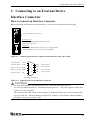
Interface Connector................................................................................................................................... 13
How to Connect an Interface Connector ......................................................................................... 13
Types of Cable and Example Connections............................................................................................. 14
4.
FUNCTIONS
15
Communication Function......................................................................................................................... 15
Serial Data Transmission .................................................................................................................. 15
RS-422A/485 Control Lines............................................................................................................. 15
Send and Receive Data Buffers........................................................................................................ 15
Setting the Baud Rate........................................................................................................................ 16
Automatic RTS Control Functions .................................................................................................. 18
COM-1PD(FIT)GY
iii
Other Functions......................................................................................................................................... 18
Bus Isolation ...................................................................................................................................... 18
Surge Protection ................................................................................................................................ 18
5.
USING THE MODULE
19
Compatible and Enhanced Modes........................................................................................................... 19
Details on I/O Ports and Registers.......................................................................................................... 21
Interrupt Vector Registers........................................................................................................................ 25
Using an Interrupt ..................................................................................................................................... 26
Examples.................................................................................................................................................... 27
Compatible Mode .............................................................................................................................. 28
Enhanced Mode ................................................................................................................................. 31
6.
SYSTEM REFERENCE
35
Block Diagram .......................................................................................................................................... 35
Equivalence Circuit .................................................................................................................................. 36
Specification.............................................................................................................................................. 37
External Dimensions................................................................................................................................. 38
iv
COM-1PD(FIT)GY
1. Before Using the Product
1. Before Using the Product
This chapter provides information you should know before using the product.
About the Module
The COM-1PD(FIT)GY performs serial communication with an external device in compliance with
RS-422A/485, capable of serving as COM3 or COM4 of an F&eIT series microcontroller module
CPU-SBxx(FIT)GY.
Please read this manual carefully to create application programs and configure the system, such as
setting the switches and connecting it to external devices.
Features
-
RS-422A/485 serial communication ports
-
The communication lines for each channel are electrically isolated from each other and from the
module.
-
Baud rates can be selected from 50 to 921,600 bps by means of software. For each channel, a
separate baud rate can be specified.
-
A baud rate can be set for each channel by software.
-
Each channel is equipped with separate 128-byte FIFO buffers for transmit and receive.
-
Driver software is supplied to allow the serial ports to be used as standard Windows or Linux COM
ports.
-
The data transfer mode (full duplex or half duplex) can be set by a switch.
-
The board includes a 100Ω terminating resistor required for multi-drop (party line) connections.
The resistor for each channel can be inserted into the signal line by a switch.
-
Surge protection is provided for each RS-422A/485 signal line.
-
Similar to other F&eIT series products, the system, in the module itself, incorporates a 35-mm DIN
rail mounting mechanism as a standard item. A connection to a controller module can be effected on
a lateral, stack basis in a unique configuration, which permits a simple, smart system configuration
without the need for a backplane board.
COM-1PD(FIT)GY
1
1. Before Using the Product
Customer Support
CONTEC provides the following support services for you to use CONTEC products more efficiently and
comfortably.
Web Site
Japanese
English
Chinese
http://www.contec.co.jp/
http://www.contec.com/
http://www.contec.com.cn/
Latest product information
CONTEC provides up-to-date information on products.
CONTEC also provides product manuals and various technical documents in the PDF.
Free download
You can download updated driver software and differential files as well as sample programs available in
several languages.
Note! For product information
Contact your retailer if you have any technical question about a CONTEC product or need its price,
delivery time, or estimate information.
Limited One-Year Warranty
CONTEC Interface modules are warranted by CONTEC CO., LTD. to be free from defects in material
and workmanship for up to one year from the date of purchase by the original purchaser.
Repair will be free of charge only when this device is returned freight prepaid with a copy of the original
invoice and a Return Merchandise Authorization to the distributor or the CONTEC group office, from
which it was purchased.
This warranty is not applicable for scratches or normal wear, but only for the electronic circuitry and
original modules. The warranty is not applicable if the device has been tampered with or damaged
through abuse, mistreatment, neglect, or unreasonable use, or if the original invoice is not included, in
which case repairs will be considered beyond the warranty policy.
How to Obtain Service
For replacement or repair, return the device freight prepaid, with a copy of the original invoice. Please
obtain a Return Merchandise Authorization Number (RMA) from the CONTEC group office where you
purchased before returning any product.
*
No product will be accepted by CONTEC group without the RMA number.
Liability
The obligation of the warrantor is solely to repair or replace the product. In no event will the warrantor
be liable for any incidental or consequential damages due to such defect or consequences that arise from
inexperienced usage, misuse, or malfunction of this device.
2
COM-1PD(FIT)GY
1. Before Using the Product
Safety Precautions
Understand the following definitions and precautions to use the product safely.
Safety Information
This document provides safety information using the following symbols to prevent accidents resulting in
injury or death and the destruction of equipment and resources. Understand the meanings of these labels
to operate the equipment safely.
DANGER
DANGER indicates an imminently hazardous situation which, if not avoided, will
result in death or serious injury.
WARNING
WARNING indicates a potentially hazardous situation which, if not avoided, could
result in death or serious injury.
CAUTION
CAUTION indicates a potentially hazardous situation which, if not avoided, may
result in minor or moderate injury or in property damage.
COM-1PD(FIT)GY
3
1. Before Using the Product
Handling Precautions
CAUTION
Take the following precautions when handling this module.
-
Do not modify the module. CONTEC will bear no responsibility for any problems, etc., resulting
from modifying this module.
-
Do not use or store the equipment in a hot or cold place, or in a place that is subject to severe
temperature changes. (Operating temperature range: 0 to 50°C)
-
Do not use or store the equipment in a place subject to direct sunlight or near a heating device, such
as a stove.
-
Do not use or store the equipment in a dusty or humid place. (Operating humidity range: 10 to
90%RH, no condensation)
-
As this product contains precision electronic components, do not use or store in environments
subject to shock or vibration.
-
Do not use or store the product near equipment generating a strong magnetic field or radio waves.
-
If you notice any strange odor or overheating, please unplug the power cord immediately.
-
In the event of an abnormal condition or malfunction, please consult the dealer from whom the
equipment was purchased.
-
To avoid electric shock, please do not touch the system with a wet hand.
-
Do not open the module casing. CONTEC will disclaim any responsibility for equipment whose
casing has been opened.
-
To prevent damage, please do not subject the module to impact or bend it.
-
To prevent contact malfunction, please do not touch the metallic pins on the external module
connector.
-
The module contains switches that need to be properly set. Before using the module, please check
its switch settings.
-
To avoid malfunction, please do not change the module switch settings in an unauthorized manner.
-
"Do not operate the device module when the power for the Controller Module is on.
To avoid malfunction, please be sure to turn off the power for the Controller Module."
4
COM-1PD(FIT)GY
1. Before Using the Product
Environment
Use this product in the following environment. If used in an unauthorized environment, the module may
overheat, malfunction, or cause a failure.
Operating temperature
0 to 50°C
Humidity
10% to 90%RH (No condensation)
Corrosive gases
None
Floating dust particles
Not to be excessive
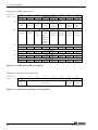
Inspection
Inspect the product periodically as follows to use it safely.
*The ventilation slits are not covered,
and neither dust nor alien substance is attached to the ventilation slits
TX
BC D
EF
MODE
1 2 3 4 5 6 7 8 910
3 45
TER M
0 12
8 9A
RX
Device
ID
67
CH0
CH0
COM-1PD
Storage
When storing this product, keep it in its original packing form.
(1) Put the module in the storage bag.
(2) Wrap it in the packing material, then put it in the box.
(3) Store the package at room temperature at a place free from direct sunlight, moisture, shock,
vibration, magnetism, and static electricity.
Disposal
When disposing of the product, follow the disposal procedures stipulated under the relevant laws and
municipal ordinances.
COM-1PD(FIT)GY
5
1. Before Using the Product
6
COM-1PD(FIT)GY
2. Module Nomenclature and Settings
2. Module Nomenclature and Settings
Nomenclature of Module Components
Figure 2.1. shows the names of module components. In the figure, the indicated switch settings
represent factory settings.
CH0
RX
TX
C
6
0 2
Device
ID
E
Device ID
8 A
LED Indicator
TERM
MODE
Interface connector
1 2 3 4 5 6 7 8 910
4
Transmission
mode terminators
CH0
COM-1PD
Figure 2.1. Names of module components
COM-1PD(FIT)GY
7
2. Module Nomenclature and Settings
Setting a Device ID
Depending on the specific Device ID that is set, the COM-1PD(FIT)GY can be switched over between
the compatible mode and the enhanced mode.
Table 2.1 shows the relationship between Device IDs and the modes.
For a description of the compatible and enhanced modes, see Chapter 4, "Using the Module".
The factory setting is [0], in which the COM-1PD(FIT)GY can be used as a COM3 standard port.
Setup Method
A device ID can be set by turning the rotary switch on the device face.
To set a device ID, turn the switch knob.
C
8
0
Device
ID
Factory settings:
(Device ID = 0)
4
Figure 2.2. Setting a Device ID
Table 2.1. I/O Address
ID No.
Ch0
I/O address(h)
Interrupt
0
03E8 to 03EF
IRQ5
1
03E8 to 03EF
Not Used
2
02E8 to 02EF
IRQ7
3
02E8 to 02EF
Not Used
4
01A0 to 01A7
IRQ5
5
01A0 to 01A7
IRQ7
6
02A0 to 02A7
IRQ5
7
02A0 to 02A7
IRQ7
8
9800 to 9807
IRQ9
9
9820 to 9827
IRQ5
A
9840 to 9847
IRQ7
B
9860 to 9867
Not Used
C
Reserved
Reserved
D
Reserved
Reserved
E
Reserved
Reserved
F
Reserved
Reserved
8
COM-1PD(FIT)GY
2. Module Nomenclature and Settings
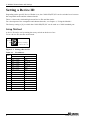
Setting Transmission Mode
The data transfer mode setting switch is used to switch between full duplex and half duplex and to
specify whether to use RTS/CTS in full duplex mode. Set the appropriate data transfer mode for the
device with which you are communicating. Bits 1 to 5 are used to set the data transfer mode. Always set
bit 6 is to OFF.
Setting Procedure
Table 2.2. Setting Transmission Mode
Full duplex
[Full]
When there are no
RTS and CTS
RTS
TXD is only used for data
transmission; the sending
and receiving modes should
be switched over using
the modem control
register.
1 2 3 4 5 6
ON
ON
Setting
1 2 3 4 5 6 7
With above setting, RTS and
CTS are connected in the
board.
Communication is available
without wiring of RTS and
CTS.
8 9 10
8 9 10
7 8 9 10
CTS
When there are RTS and CTS
RTS
CTS
1 2 3 4 5 6 7
Half duplex
[Half]
ON
Transmission
mode
Factory
setting
To connect RTS and CTS to
the other unit,
communication is available.
CAUTION
Do not use with bits 1 and 2 both set ON as this may result in damage to the module.
COM-1PD(FIT)GY
9
2. Module Nomenclature and Settings
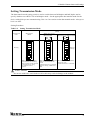
Setting of Terminator
The terminator setting switch controls whether or not a terminator is inserted into each signal line. Set
the terminators on or off in accordance with the devices with which you are communicating. The
terminators on the module are 100Ω resistors. See Figure 2.4 for details on how to use terminators in a
multi-drop (party line) connection.
Each bit in the switch corresponds to a different signal line: bit 7 for RxD, bit 8 for CTS, bit 9 for TxD,
and bit 10 for RTS.
Setting Procedure
If you wish to use a terminator of other than 100Ω, set the terminator switch OFF and insert an external
terminator.
Not inserted
[Term OFF]
1 2 3 4 5 6 7 8 9 10
ON
Setting
ON
Inserted
[Term ON]
1 2 3 4 5 6 7 8 9 10
Table 2.3. Setting of Terminator
Factory
setting
Figure 2.3. B or C
(Other than both
terminators of the line)
Figure 2.3. A or D
(Both terminators
of the line)
Terminator
Terminator
(A)
(B)
(C)
(D)
Figure 2.3. Party Line Connection
CAUTION
When the data transfer mode is set to half duplex, only set bit 9 ON. Communications may not
function if other bits are set ON.
10
COM-1PD(FIT)GY
2. Module Nomenclature and Settings
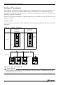
The figure below shows the circuit associated with the data transfer mode setting switch and terminator
setting switch.
1 2 3 4 5 6
162850
or Equivalent
SOUT
Terminator
7 8 9 10
Terminator
1/2W 100Ω
Data transmission
mode
TxD+
TxD-
SIN
RxD+
RxD-
CTS
CTS+
CTS-
RTS
RTS+
RTS-
DCD
DTR
DSR
RI
Figure 2.4. Setting Switch Circuits
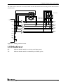
LED Indicator
RX:
Indicates that the module is receiving serial data (green).
TX:
Indicates that the module is transmitting serial data (green).
COM-1PD(FIT)GY
11
2. Module Nomenclature and Settings
12
COM-1PD(FIT)GY
3. Connecting to an External Device
3. Connecting to an External Device
Interface Connector
How to Connect an Interface Connector
When connecting the Module to an external device, you can use the supplied connector plug
RX
TX
C
E
6
0 2
8 A
CH0
Device
ID
MODE
1 2 3 4 5 6 7 8 910
4
TERM
Lock nut: UNC#4-40(inch screw)
Connector used
- DELC-J9SAF-20L9 (Female Connector type)
(mfd.by JAE) equivalent
Applicable
- 17JE-23090-02(D8C) (Male Connector type) (mfd.by DDK)
CH0
- CN5-D9M(Male Connector type) (mfd.by CONTEC)
COM-1PD
Figure 3.1. Connecting an interface connector and connectors that can be used
Transmit Data-
TxD-
1
Transmit Data+
TxD+
2
Request to Send- RTS-
3
Request to Send+ RTS+
4
Signal Ground
5
SG
6
RxD-
7
RxD+
Receive Data+
8
CTS+
Clear to Send+
9
CTS-
Clear to Send-
Receive Data-
CH0
(D-SUB9 pin(Female))
Figure 3.2. Signal Layout on the Interface Connector
CAUTION
-
For TxD, RxD, and RTS, big numbered pins are + and small numbered pins are -.
For CTS, big numbered pins are - and small numbered pins are +. This is the opposite of the other
signals, but is not a misprint.
-
The external metal frame (shell) of the connector is insulated from the unit, or not in contact with
any part of the unit. When grounding is required, for example, as data transfer remains unstable,
ground the remote device to the earth.
COM-1PD(FIT)GY
13
3. Connecting to an External Device
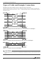
Types of Cable and Example Connections
The figures below show examples of how to connect the cable for the module.
The RS-422A/485 interface works based on a differential signal whereby the signal is carried by the
potential difference between two lines (+ and -). Using twisted pair cable is recommended to improve
resistance to noise.
TxD+
TxD+
TxD-
TxD-
RxD+
RxD+
RxD-
RxD-
RTS+
RTS+
RTS-
RTS-
CTS+
CTS+
CTS-
CTS-
SG
SG
External device
Figure 3.3. Example Connection RTS and CTS to a External Device in Full Duplex
TxD+
TxD+
TxD-
TxD-
RxD+
RxD+
RxD-
RxD-
SG
SG
External device
Figure 3.4. Example Connection Oneself loop to RTS and CTS in Full Duplex
TxD+
TxD+
TxD-
TxD-
SG
SG
External device
Figure 3.5. Example Connection in Half Duplex
CAUTION
If connecting between external devices and this board with faulty wiring, it will become the cause of
failure.
14
COM-1PD(FIT)GY
4. Functions
4. Functions
This section describes the functions of the module.
Communication Function
Serial Data Transmission
Sends and receives data in accordance with the RS-422A/485 standard.
The baud rate for each channel can be set independently in the range 2 to 921,600bps by software.
RS-422A/485 Control Lines
All ports include the RTS+, RTS-, CTS+, and CTS- control lines.
The lines can be controlled or monitored by software from the application
Send and Receive Data Buffers
Each channel has a separate 128-byte send and 128-byte receive buffer.
The buffers operate as FIFO buffers and help reduce the load on the CPU for high-speed
communications or system operation.
The FIFO trigger size is a data buffer size that determines the timing of generating a hardware interrupt.
Increasing the FIFO trigger size decreases the number of times hardware interrupts occur for data
transmission and reception, thereby reducing the load on the CPU.
However, this delays the timing of transmitting data to the remote device and the timing of notifying an
application of data reception because actual transmission and reception take place after a certain amount
of data has been collected.
In contrast, decreasing the FIFO trigger size or disabling FIFO memory shortens the timing of data
transmission and reception but may increase the load on the CPU or miss some receiving data.
Since the FIFO trigger size is variable, adjusting it depending on the system results in optimum
performance.
COM-1PD(FIT)GY
15
4. Functions
Setting the Baud Rate
The output baud rate can be set by setting the appropriate value to the Baud Rate Generator register. The
available setting range depends on which clock mode is used.
Clock 3 mode: 15 to 921,600bps
Clock 2 mode: 8 to 460,800bps
Clock 1 mode: 4 to 230,400bps
Clock 0 mode: 2 to 115,200bps
However, some baud rate values do not have a corresponding Baud Rate Generator register setting. If
the result of substituting the baud rate into the equation below is an integer, then that baud rate can be set.
If the result contains a fractional part, the baud rate cannot be set.
Clock 3 mode
921600 ÷ Desired baud rate = Division register setting value
Ex.) 921600 ÷ 9600bps = 96 (As the result is an integer, this baud rate can be set.)
921600 ÷ 128000bps = 7.2 (As the result contains a fractional part, this baud rate cannot be set.)
Clock 2 mode
460800 ÷ Desired baud rate = Division register setting value
Ex.) 460800 ÷ 9600bps = 48 (As the result is an integer, this baud rate can be set.)
460800 ÷ 128000bps = 3.6 (As the result contains a fractional part, this baud rate cannot be set.)
Clock 1 mode
230400 ÷ Desired baud rate = Division register setting value
Ex.) 230400 ÷ 9600bps = 24 (As the result is an integer, this baud rate can be set.)
230400 ÷ 128000bps = 1.8 (As the result contains a fractional part, this baud rate cannot be set.)
Clock 0 mode
115200 ÷ Desired baud rate = Division register setting value
Ex.) 115200 ÷ 9600bps = 12 (As the result is an integer, this baud rate can be set.)
115200 ÷ 76800bps = 1.5 (As the result contains a fractional part, this baud rate cannot be set.)
CAUTION
See Chapter 5 “Interrupt Vector Registers” for selecting the clock frequency (1.8432, 3.6864,
7.3728, or 14.7456 MHz).
For use in compatible mode, clock 0 (1.8432 MHz) is used as a fixed setting.
16
COM-1PD(FIT)GY
4. Functions
Refer to the following baud rate setting examples. Baud rates other than those listed
below can also be set if they produce a valid setting value in the equation described above.
Table 4.1. Baud Rate Generator Programming Table
Output
baud rate
Clock 0 mode
Clock 0 mode
Clock 0 mode
Clock 0 mode
(1.8432MHz)
(3.6864MHz)
(7.3728MHz)
(14.7456MHz)
Baud Rate
Setup
Baud Rate
Setup
Baud Rate
Setup
Baud Rate
Setup
Generator
error
Generator
error
Generator
error
Generator
error
register
(%)
register
(%)
register
(%)
register
(%)
2
57600
-
4
28800
-
57600
-
5
23040
-
46080
-
8
14400
-
28800
-
57600
-
15
7680
-
15360
-
30720
-
61440
-
50
2304
-
4608
-
9216
-
18432
-
75
1536
-
3072
-
6144
-
12288
-
110
1047
0.026
2094
0.026
4189
0.0022
8378
0.0022
134.5
857
0.058
1713
0.0006
3426
0.0006
6852
0.0006
150
768
-
1536
-
3072
-
6144
-
300
384
-
768
-
1536
-
3072
-
600
192
-
384
-
768
-
1536
-
1200
96
-
192
-
384
-
768
-
1800
64
-
128
-
256
-
512
-
2000
58
0.68
115
0.17
230
0.17
461
0.04
2400
48
-
96
-
192
-
384
-
3600
32
-
64
-
128
-
256
-
4800
24
-
48
-
96
-
192
-
7200
16
-
32
-
64
-
128
-
9600
12
-
24
-
48
-
96
-
14400
8
-
16
-
32
-
64
-
19200
6
-
12
-
24
-
48
-
28800
4
-
8
-
16
-
32
-
38400
3
-
6
-
12
-
24
-
57600
2
-
4
-
8
-
16
-
3
-
6
-
12
-
2
-
4
-
8
-
3
-
6
-
1
-
2
-
4
-
1
-
2
-
1
-
76800
115200
1
-
153600
230400
460800
921600
COM-1PD(FIT)GY
17
4. Functions
Automatic RTS Control Functions
This function applies to half duplex mode communications.
As half duplex means that the same line is used for sending and receiving, the RTS and CTS signals are
used to switch between sending and receiving. Normally, RTS is set by writing to the corresponding
register bit, but on this module it is controlled by hardware. This reduces the load on the CPU.
Other Functions
Bus Isolation
The communication lines are electrically isolated from each other and from the PC.
This isolation prevents electrical disturbances from occurring between the Module and the external
circuitry.
The Module can therefore be used comfortably even when line noise can be easily generated to
seemingly cause the Module to malfunction or break.
Surge Protection
As surge protection is provided on all RS-422A/485 control lines, you can safely use the modules in
environments where you are concerned about surges causing incorrect operation or damage to the PC.
18
COM-1PD(FIT)GY
5. Using the Module
5. Using the Module
Compatible and Enhanced Modes
The COM-1PD(FIT)GY can operate in two modes: the compatible mode, in which the
COM-1PD(FIT)GY, when connected to a CPU-SBxx(FIT)GY, acts as a standard serial port; and the
enhanced mode, in which the COM-1PD(FIT)GY operates under CONTEC's unique control method.
Before building a system using the COM-1PD(FIT)GY, a working understanding of the features of these
modes may be in order.
Compatible Mode
The COM-1PD(FIT)GY can use two channels as standard serial ports.
COM-1PD(FIT)GY can be assigned to COM3 or COM4.
The module uses the I/O addresses assigned for a standard serial port. As the module is handled as the
standard serial port, it can run under other driver software that can operate standard serial ports.
Although OS-dependent, the I/O addresses in the COM-1PD(FIT)GY can be recognized by the system
and used as standard ports. You can use these addressed by checking the system settings.
Enhanced Mode
The enhanced mode operates the COM-1PD(FIT)GY by using CONTEC's unique control method.
For I/O addresses, CONTEC-designated addresses must be used.
Notice that the enhanced mode requires different programming than the compatible mode.
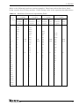
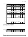
Table 5.1. I/O Address
ID No.
CH0
Function
I/O address(h)
Interrupt Level
0
COM3
03E8 to 03EF
IRQ5
1
COM3
03E8 to 03EF
Not Used
2
COM4
02E8 to 02EF
IRQ7
3
COM4
02E8 to 02EF
Not Used
4
Enhanced mode
01A0 to 01A7
IRQ5
5
Enhanced mode
01A0 to 01A7
IRQ7
6
Enhanced mode
02A0 to 02A7
IRQ5
7
Enhanced mode
02A0 to 02A7
IRQ7
8
Enhanced mode
9800 to 9807
IRQ9
9
Enhanced mode
9820 to 9827
IRQ5
A
Enhanced mode
9840 to 9847
IRQ7
B
Enhanced mode
9860 to 9867
Not Used
C
Reserved
Reserved
Reserved
D
Reserved
Reserved
Reserved
E
Reserved
Reserved
Reserved
F
Reserved
Reserved
Reserved
COM-1PD(FIT)GY
19
5. Using the Module
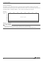
I/O Ports and Registers
The module uses the XR16C2850 (Exar Corporation) upward compatible with the 16550 UART.
For details on the internal registers of the XR16C2850 and its control, refer to the XR16C2850 data sheet.
In enhanced mode, “starting I/O address + 1Fh” is used as an interrupt vector register.
I/O Ports
Starting I/O
address
D7
D6
D5
D4
D3
D2
D1
D0
+0h
+1h
+2h
+3h
+4h
Channel 0 register
+5h
+6h
+7h
+1Fh
Interrupt vector register
Figure 5.1. I/O Ports
CAUTION
Each port must be accessed in bytes to conform to device specifications.
Non-byte access to any port is not allowed (such as word access or doubleword access).
20
COM-1PD(FIT)GY
5. Using the Module
Details on I/O Ports and Registers
The XR16C2850’s internal registers are port-mapped differently depending on the value set in the Line
Control Register (LCR).
The General Registers are enabled at startup or with LCR bit 7 = 0 and LCR = other than 0xBF.
The Baud Rate Registers are enabled with LCR bit 7 = 1.
The Enhanced Registers are enabled with LCR = 0xBF.
Input port 1 (General Registers)
Starting I/O
address
D7
D6
D5
+0h
D4
D3
D2
D1
D0
Receive Holding Register (RHR)
Data Bit 7 Data Bit 6 Data Bit 5 Data Bit 4 Data Bit 3 Data Bit 2 Data Bit 1 Data Bit 0
+1h
Interrupt Enable Register (IER)
CTS
RTS
Xoff
Sleep
MODEM
Receive
Transmit
Receive
Interrupt
(*2)
Interrupt
(*2)
Interrupt
(*2)
Mode
(*2)
Status
Interrupt
Line
Status
Holding
Register
Holding
Register
Int
Status
Interrupt
+2h
Interrupt Status Register (ISR)
FIFOs
Enable
FIFOs
Enable
-RTS,
-CTS
+3h
Xoff
Int
Priority
Int
Priority
Int
Priority
Bit 2
Bit 1
Bit 0
Line Control Register (LCR)
Divisor
Set
Set
Even
Parity
Stop
Word
Word
Latch
Enable
Break
Parity
Parity
Enable
Bits
Length
Bit 1
Length
Bit 0
Clock
Prescaler
IR
Mode
Xon
Any
Loop
Back
-OP2 and
INT
Out 1
0:INT
-RTS
-DTR
Select
(*2)
Enable
(*2)
(*2)
Enable
Enable
Enable
1:INT
Overrun
Error
Receive
Data
+4h
Modem Control Register (MCR)
Disable
(*1)
+5h
Line Status Register (LSR)
FIFO
Error
THR&
TSR
THR
Empty
Break
Interrupt
Framing
Error
Parity
Error
Empty
Ready
+6h
Modem Status Register (MSR)
-CD
-RI
-DSR
Bit 7
Bit 6
Bit 5
+7h
*3
Delta
-RI
Delta
-DSR
Data
-CTS
Bit 4
Bit 3
Bit 2
Bit 1
Bit 0
Bit 1
Bit 0
FIFO Level Counter (FLVL) (*3)
Bit 7
*2
Delta
-CD
Scratch Pad Register (SPR)
+7h
*1
-CTS
Bit 6
Bit 5
Bit 4
Bit 3
Bit 2
For details, see the “Using an Interrupt” section.
These bits are enabled with EFR bit 4 = 1.
These registers are enabled with FCTR bit 6 = 1.
Figure 5.2. Input port (General Registers)
COM-1PD(FIT)GY
21
5. Using the Module
Input port 2 (Baud Rate Registers)
Starting I/O
address
D7
D6
D5
D4
+0h
D3
D2
D1
D0
Bit 2
Bit 1
Bit 0
LSB of Divisor Latch (DLL)
Bit 7
Bit 6
Bit 5
+1h
Bit 4
Bit 3
MSB of Divisor Latch (DLM)
Bit 15
Bit 14
Bit 13
Bit 12
Bit 11
Bit 10
Bit 9
Bit 8
D4
D3
D2
D1
D0
Trig/FC
Trig/FC
Trig/FC
Figure 5.3. Input port (Baud Rate Registers)
Input port 3(Enhanced Registers)
Starting I/O
address
D7
D6
D5
+0h
FIFO Level Counter
Trig/FC
Trig/FC
Trig/FC
+1h
Trig/FC
Trig/FC
Feature Control Register (FCTR)
Rx/Tx
SCPAD
Trig
Trig
RS485
IrRx
-RTS
-RTS
Mode
Swap
Bit 1
Bit 0
Auto
control
Inv.
Delay
Bit 1
Delay
Bit 0
Auto
-CTS
Auto
-RTS
Special
Char,
Enable
IER
Cont-3
Tx, Rx
Cont-2
Tx, Rx
Cont-1
Tx, Rx
Cont-0
Tx, Rx
select
Bits 4-7,
ISR, FCR
Control
Control
Control
Control
Bit 2
Bit 1
Bit 0
Bit 10
Bit 9
Bit 8
Bit 2
Bit 1
Bit 0
+2h
Enhanced Feature Register (EFR)
Bits 4-5,
MCR
Bits 5-7
+4h
Xon-1 Word
Bit 7
Bit 6
Bit 5
Bit 4
+5h
Bit 3
Xon-2 Word
Bit 15
Bit 14
Bit 13
Bit 12
+6h
Bit 11
Xoff-1 Word
Bit 7
Bit 6
Bit 5
Bit 4
+7h
Bit 3
Xoff-2 Word
Bit 15
Bit 14
Bit 13
Bit 12
Bit 11
Bit 10
Bit 9
Bit 8
D4
D3
D2
D1
D0
Figure 5.4. Input port (Enhanced Registers)
Input port 4 (Interrupt vector register)
Starting I/O
address
D7
D6
D5
Interrupt vector register
+1Fh
Fixed at
“0”
(Reserved)
CH0
Interrupt
Figure 5.5. Input port (Interrupt vector register)
22
COM-1PD(FIT)GY
5. Using the Module
Output port 1(General Registers)
Starting I/O
address
D7
D6
+0h
D5
D4
D3
D2
D1
D0
Transmit Holding Register (THR)
Data Bit 7 Data Bit 6 Data Bit 5 Data Bit 4 Data Bit 3 Data Bit 2 Data Bit 1 Data Bit 0
+1h
Interrupt Enable Register (IER)
CTS
RTS
Xoff
Sleep
MODEM
Receive
Transmit
Receive
Interrupt
(*2)
Interrupt
(*2)
Interrupt
(*2)
Mode
(*2)
Status
Interrupt
Line
Status
Holding
Register
Holding
Register
FIFO
Enable
Interrupt
+2h
FIFO Control Register (FCR)
RCVR
RCVR
TX
Trigger
(MSB)
+3h
TX
Trigger
DMA
Mode
XMIT
FIFO
RCVR
FIFO
(LSB)
Select
Reset
Reset
Line Control Register (LCR)
Divisor
Set
Set
Even
Parity
Stop
Word
Word
Latch
Enable
Break
Parity
Parity
Enable
Bits
Length
Bit 1
Length
Bit 0
Clock
Prescaler
IR
Mode
Xon
Any
Loop
Back
-OP2 and
INT
Out 1
0:INT
-RTS
-DTR
Select
(*2)
Enable
(*2)
(*2)
Enable
Enable
Enable
1:INT
Bit 1
Bit 0
Alt.RX/TX
RX/TX
FIFO
Count
FIFO
Count
D2
D1
D0
Bit 2
Bit 1
Bit 0
Bit 10
Bit 9
Bit 8
+4h
Modem Control Register (MCR)
Disable
(*1)
+5h
Disable
+6h
Disabled
+7h
Scratch Pad Register (SPR)
Bit 7
Bit 6
+7h
Bit 5
Bit 4
Bit 3
Bit 2
Enhanced Mode Select Registers (EMSR) (*3)
Reserved
Reserved
RTS Hyst
RTS Hyst
Bit 3
Bit 2
Reserved
Reserved
*1
For details, see the “Using an Interrupt” section.
These bits are enabled with EFR bit 4 = 1.
*3
These registers are enabled with FCTR bit 6 = 1.
Figure 5.6. Output port (General Registers)
*2
Output port 2(Baud Rate Registers)
Starting I/O
address
D7
D6
D5
+0h
D4
D3
LSB of Divisor Latch (DLL)
Bit 7
Bit 6
Bit 5
+1h
Bit 4
Bit 3
MSB of Divisor Latch (DLM)
Bit 15
Bit 14
Bit 13
Bit 12
Bit 11
Figure 5.7. Output port (Baud Rate Registers)
COM-1PD(FIT)GY
23
5. Using the Module
Output port 3(Enhanced Registers)
Starting I/O
address
D7
D6
D5
+0h
D4
D3
D2
D1
D0
Trig/FC
Trig/FC
Trig/FC
FIFO Level Counter
Trig/FC
Trig/FC
Trig/FC
+1h
Trig/FC
Trig/FC
Feature Control Register (FCTR)
Rx/Tx
SCPAD
Trig
Trig
RS485
IrRx
-RTS
-RTS
Mode
Swap
Bit 1
Bit 0
Auto
control
Inv.
Delay
Bit 1
Delay
Bit 0
Auto
Auto
Special
Enable
Cont-3
Cont-2
Cont-1
Cont-0
-CTS
-RTS
Char,
select
IER
Bits 4-7,
Tx, Rx
Control
Tx, Rx
Control
Tx, Rx
Control
Tx, Rx
Control
Bit 2
Bit 1
Bit 0
Bit 10
Bit 9
Bit 8
Bit 2
Bit 1
Bit 0
Bit 11
Bit 10
Bit 9
Bit 8
D3
D2
D1
D0
Clock
selection
Clock
selection
Bit 1
Bit 0
+2h
Enhanced Feature Register (EFR)
ISR, FCR
Bits 4-5,
MCR
Bits 5-7
+4h
Xon-1 Word
Bit 7
Bit 6
Bit 5
Bit 4
+5h
Bit 3
Xon-2 Word
Bit 15
Bit 14
Bit 13
Bit 12
+6h
Bit 11
Xoff-1 Word
Bit 7
Bit 6
Bit 5
Bit 4
+7h
Bit 3
Xoff-2 Word
Bit 15
Bit 14
Bit 13
Bit 12
Figure 5.8. Output port (Enhanced Register)
Output port 4(Interrupt Vector Registers)
Starting I/O
address
D7
+1Fh
D6
D5
D4
Interrupt Vector Registers
Fixed at
“0”
(Reserved)
Figure 5.9. Output port (Interrupt Vector Registers)
24
COM-1PD(FIT)GY
5. Using the Module
Interrupt Vector Registers
- Output port
Starting I/O
address
+1Fh
D7
D6 to D2
(Reserved)
D1 D0
Clock selection(see "setting a Baud Rate")
00: Clock 0 mode(1.8432MHz)
01: Clock 0 mode(3.6864MHz)
10: Clock 0 mode(7.3728MHz)
11: Clock 0 mode(14.7456MHz)
Fixed at "0"
- Input port
Starting I/O
address
+1Fh
D7
D6 to D1
D0
(Reserved)
CH0 interrupt(see"Using an Interrupt")
0: Interrupt detected
1: No interrupts
Fixed at "0"
Figure 5.10. Interrupt Vector Registers
COM-1PD(FIT)GY
25
5. Using the Module
Using an Interrupt
Compatible Mode
When the Module is operated in the compatible mode, channel CH0 is assigned to standard I/O addresses
COM3 and COM4, respectively. The interrupt levels will be IRQ5 for COM3 and IRQ7 for COM4.
Enhanced Mode
When the Module is being used in enhanced mode, interrupt generation can be checked with the interrupt
vector register (IVR). The Device ID switch is used to specify the interrupt line to be used.
When accepting an interrupt, you can check, by reading the IVR, whether the interrupt has been
generated within the interrupt service routine. Before exiting from the executed interrupt service, read
the IVR again to check for any pending interrupt.
The XR16C2850 contains an internal register to enable itself for interrupts (make them available) or to
check whether any interrupt has been generated. For using the register, refer to the data sheet for the
XR16C2850 supplied by Exar Corporation.
For setting to use interrupts, use the D2 bit in the modem control register (MCR).
D2 bit of MCR
26
Write 0 : Enable(when the power is turned on)
Write 1 : Disable
COM-1PD(FIT)GY
5. Using the Module
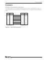
Examples
Following is a COM-1PD(FIT)GY sample program.
The sample program executes transmission and reception between two COM-1PD(FIT)GY units. To
connect RTS and CTS to an external device in full-duplex mode, use a connection cable as illustrated
below.
Code
Pin
Pin
SG
5
5
Code
SG
TxD+
2
7
RxD+
TxD-
1
6
RxD-
RxD+
7
2
TxD+
RxD-
6
1
TxD-
RTS+
4
8
CTS+
RTS-
3
9
CTS-
CTS+
8
4
RTS+
CTS-
9
3
RTS-
1st set (CH0)
2nd set (CH1)
Figure 5.11. Cable Connection Diagram
COM-1PD(FIT)GY
27
5. Using the Module
Compatible Mode
Flowchart
Start
(1)
Set Baud Rate
Generator
CH0 LSR D5
Bit = 1
Set transmission
format
Send CH0 data
No
Yes
WAIT time
CH1 LSR D0
Bit = 1
Yes
Set modem control
output
Receive CH1 data
Line status register
dummy READ
Final data
RECEIVE register
dummy READ
Show data
Interrupt ID register
dummy READ
CH1 LSR D5
Bit = 1
Modem status register
dummy READ
Final channel
No
Yes
Send CH1 data
No
CH0 LSR D0
Bit = 1
Yes
(1)
No
No
Yes
Receive CH0 data
Final data
Show data
End
28
COM-1PD(FIT)GY
5. Using the Module
Sample Program
/*===========================================================================
Sample program 1
-- UNIT0 <=> UNIT1 Loop Test -UNIT No.
DEVICE ID:
Mode:
Channel 0:
Baud Rate:
Interrupt:
0
1
0
2
Compatible Mode
03E8H (COM3) 02E8H (COM4)
115,200 bps
N/A
========================================================================== */
#include <stdio.h>
#include <conio.h>
/* ----- Constant ---------------------------------------------------------- */
#define CH
2
/* no. of channels */
#define NUM
10
/* data of total number */
#define BPS
1
/* baud rate */
unsigned char
rbuf[CH][NUM];
/* receive buffer */
unsigned int ADR[CH] = {0x3e8, 0x2e8}; /* I/O address */
unsigned int rcnt[CH] = {0, 0};
/* receive count */
/* ----- Prototype --------------------------------------------------------- */
void main( void );
/* ----- Main -------------------------------------------------------------- */
void main( void )
{
unsigned char
i, j;
int
dummy;
for(i = 0; i < CH; i
outp( ADR[i]+0x3,
outp( ADR[i]+0x0,
outp( ADR[i]+0x1,
outp( ADR[i]+0x3,
outp( ADR[i]+0x3,
++) {
/* RS-232C initialize */
0x80 );
/* Line Control Register (DLAB SET) */
BPS & 0xff ); /* Divisor Latch (Baud Rate SET) */
(BPS >> 8) & 0xff );
0x0 );
/* Line Control Register (DLAB RESET) */
0x7 );
/* Line Control Register */
/* ( Bit 0,1 ... Word Length = 8 bit ) */
/* ( Bit 2 ..... 2 stop bit
) */
for(j = 0; j < 10; j++)
/* hardware wait */
dummy = inp( 0x2ef );
outp(
dummy
dummy
dummy
dummy
outp(
ADR[i]+0x4, 0x3 );
= inp( ADR[i]+0x5 );
= inp( ADR[i]+0x0 );
= inp( ADR[i]+0x2 );
= inp( ADR[i]+0x6 );
ADR[i]+0x1, 0x1 );
/*
/*
/*
/*
/*
/*
MODEM Control Register (DTR . RTS) */
Line Status Register(Dummy Read) */
Receiver Buffer Register (Dummy Read) */
Interrupt ID. Register (Dummy Read) */
Modem Status Register (Dummy Read) */
Interrupt Enable Register */
}
for(j = 0; j < NUM; j++) {
/* send CH0 to CH1 */
while( !(inp( ADR[0]+0x5 ) & 0x20) );
/* transmitter empty */
outp( ADR[0]+0x0, j );
while( !(inp( ADR[1]+0x5 ) & 0x1) );
/* data ready */
rbuf[1][rcnt[1]] = (unsigned char)inp( ADR[1]+0x0 );
rcnt[1]++;
}
COM-1PD(FIT)GY
29
5. Using the Module
for(j = 0; j < NUM; j++) {
printf(" CH0:%02x -> CH1:%02x
", j, rbuf[1][j]);
if(rbuf[1][j] != j) printf("Verify Error \n");
/* verify data */
else printf("\n");
}
printf("\n");
for(j = 0; j < NUM; j++) {
/* send CH1 to CH0 */
while( !(inp( ADR[1]+0x5 ) & 0x20) );
/* transmitter empty */
outp( ADR[1]+0x0, j );
while( !(inp( ADR[0]+0x5 ) & 0x1) );
/* data ready */
rbuf[0][rcnt[0]] = (unsigned char)inp( ADR[0]+0x0 );
rcnt[0]++;
}
for(j = 0; j < NUM; j++) {
printf(" CH1:%02x -> CH0:%02x
", j, rbuf[0][j]);
if(rbuf[0][j] != j) printf("Verify Error \n");
/* verify data */
else printf("\n");
}
}
/* ---------------------------------------------------------- End of file --- */
30
COM-1PD(FIT)GY
5. Using the Module
Enhanced Mode
Flowchart
Start
Interrupt
processing
Initialize
Read interrupt
vector register
Change interrupt
vectors
CH0 LSR D5
Bit = 1
CH0 IVR D0
Bit = 0
No
No
Count number
of interrupts
Yes
Send CH0 data
Read CH0 data
Show an
interrupt count
CH0 LSR D5
Bit = 0
No
Yes
End of interrupt?
No
CH0 IVR D0
Bit = 0
Yes
No
Yes
CH1 LSR D5
Bit = 1
No
Count number
of interrupts
Yes
Send CH1 data
Read CH1 data
CH1 LSR D5
Bit = 0
Show an
interrupt count
No
Yes
End of interrupt?
No
No
IVR=FH
Yes
Yes
Restore the
interrupt vector
EOI
Show data
End
End
COM-1PD(FIT)GY
31
5. Using the Module
Sample Program
/*
===========================================================================
Sample program 2
-- UNIT0 <=> UNIT1 Loop Test -UNIT No.
DEVICE ID:
Mode:
Channel 0:
Baud Rate:
Interrupt:
0
1
4
7
Enhanced Mode
1A0H
2A0H
115,200 bps
IRQ5
IRQ7
==========================================================================*/
#include <stdio.h>
#include <conio.h>
#include <dos.h>
/* ----- Constant ---------------------------------------------------------- */
#define CH
2
/* no. of channels */
#define NUM
10
/* data of total number */
#define BPS
1
/* baud rate */
#define IRQ5
0
/* IRQ5 */
#define IRQ7
1
/* IRQ7 */
volatile
volatile
volatile
volatile
unsigned
unsigned
unsigned
int
int
unsigned
char
rbuf[CH][NUM];
/* receive buffer */
int ADR[CH] = {0x1a0, 0x2a0}; /* I/O address */
int intcnt[CH] = {0, 0};
/* interrupt counter */
IrqLevel = IRQ5;
/* interrupt level */
OrgMasterImr;
/* original IMR */
char
IntVector[2] = { 0x0d, 0x0f };
/* interruput vector */
unsigned char
PicMask[2] = { 0xdf, 0x7f };
/* mask bit */
unsigned char
IsrClear[3] = { 0x65, 0x67, 0x61 };
/* ISR clear */
/* ----- Prototype --------------------------------------------------------- */
void main( void );
void Initialize( void );
/* initialize */
void ChgVect( void );
/* change vector */
void ResVect( void );
/* restore vector */
void _interrupt _far inthandler( void );
/* interrupt handler */
void ( _interrupt _far *OrgVect)();
/* original vector */
/* ----- Initialize -------------------------------------------------------- */
void Initialize( void )
{
unsigned int i, j;
int
dummy;
for(i = 0; i < CH; i++) {
outp( ADR[i]+0x3, 0x80 );
/* Line Control Register (DLAB SET) */
outp( ADR[i]+0x0, BPS & 0xff ); /* Divisor Latch (Baud Rate SET) */
outp( ADR[i]+0x1, (BPS >> 8) & 0xff );
outp( ADR[i]+0x3, 0x0 );
/* Line Control Register(DLAB RESET) */
outp( ADR[i]+0x3, 0x7 );
for(j = 0; j < 10; j++)
dummy = inp( 0x2ef );
32
/* Line Control Register */
/* ( Bit 0,1 ... Word Length = 8 bit ) */
/* ( Bit 2 ..... 2 stop bit
) */
/* hardware wait */
COM-1PD(FIT)GY
5. Using the Module
outp(
dummy
dummy
dummy
dummy
outp(
ADR[i]+0x4, 0x3 );
= inp( ADR[i]+0x5 );
= inp( ADR[i]+0x0 );
= inp( ADR[i]+0x2 );
= inp( ADR[i]+0x6 );
ADR[i]+0x1, 0x1 );
}
outp( ADR[0]+0x1f, 0x80 );
/*
/*
/*
/*
/*
/*
MODEM Control Register (DTR . RTS) */
Line Status Register (Dummy Read) */
Receiver Buffer Register (Dummy Read) */
Interrupt ID Register (Dummy Read) */
Modem Status Register (Dummy Read) */
Interrupt Enable Register */
/* Select Clock Mode */
}
/* ----- change vector ----------------------------------------------------- */
void ChgVect( void )
{
OrgVect = _dos_getvect( IntVector[IRQ5] );
OrgVect = _dos_getvect( IntVector[IRQ7] );
_disable();
_dos_setvect( IntVector[IRQ5], inthandler );
_dos_setvect( IntVector[IRQ7], inthandler );
outp( 0x21, ( OrgMasterImr = inp( 0x21 ) ) & PicMask[IRQ5] & PicMask[IRQ7] );
outp( 0x20, IsrClear[IRQ5] );
/* ISR clear */
outp( 0x20, IsrClear[IRQ7] );
/* ISR clear */
_enable();
/* enable */
}
/* ----- restore vector ---------------------------------------------------- */
void ResVect( void )
{
_disable();
/* disable */
outp( 0x21, OrgMasterImr );
_dos_setvect( IntVector[IRQ5], OrgVect );
/* restore orgvect */
_dos_setvect( IntVector[IRQ7], OrgVect );
/* restore orgvect */
_enable();
/* enable */
}
/* ----- interrupt handler ------------------------------------------------- */
void _interrupt _far inthandler( void )
{
unsigned char
sts0, sts1;
_enable();
/* enable */
do {
sts0 = (unsigned char)inp( ADR[0]+0x1f ); /* Int Vector Register */
if( !(sts0 & 0x1) ) {
/* CH0 status */
while( inp( ADR[0]+0x05 ) & 0x1) {
rbuf[0][intcnt[0]] = (unsigned char)inp( ADR[0]+0x0 );
intcnt[0]++;
/* count times of an interrupt */
}
}
} while( !(sts0 & 0xf) );
do {
sts1 = (unsigned char)inp( ADR[1]+0x1f ); /* Int Vector Register */
if( !(sts1 & 0x1) ) {
/* CH0 status */
while( inp( ADR[1]+0x05 ) & 0x1) {
rbuf[1][intcnt[1]] = (unsigned char)inp( ADR[1]+0x0 );
intcnt[1]++;
/* count times of an interrupt */
}
}
} while( !(sts1 & 0xf) );
COM-1PD(FIT)GY
33
5. Using the Module
_disable();
outp( 0x20, 0x20 );
/* disable */
/* EOI */
}
/* ------ main ------------------------------------------------------------- */
void main( void )
{
unsigned int i, j;
Initialize();
ChgVect();
/* initialize */
/* change vector */
for(j = 0; j < NUM; j++) {
/* send CH0 to CH1 */
while( !(inp( ADR[0]+0x5 ) & 0x20) );
/* transmitter empty */
outp( ADR[0]+0x0, j );
}
while(intcnt[1] < 10)
printf("Interrupt CH0:%02d CH1:%02d\n", intcnt[0], intcnt[1]);
printf("\n");
for(j = 0; j < NUM; j++) {
/* send CH1 to CH0 */
while( !(inp( ADR[1]+0x5 ) & 0x20) );
/* transmitter empty */
outp( ADR[1]+0x0, j );
}
while(intcnt[0] < 10)
printf("Interrupt CH0:%02d CH1:%02d\n", intcnt[0], intcnt[1]);
printf("\n");
ResVect();
/* restore vector */
for(j = 0; j < NUM; j++) {
printf(" CH0:%02x -> CH1:%02x
", j, rbuf[1][j]);
if(rbuf[1][j] != j) printf("Verify Error \n");
/* verify data */
else printf("\n");
}
printf("\n");
for(j = 0; j < NUM; j++) {
printf(" CH1:%02x -> CH0:%02x
", j, rbuf[0][j]);
if(rbuf[0][j] != j) printf("Verify Error \n");
else printf("\n");
}
printf("\n");
printf("Interrupt CH0:%02d CH1:%02d\n", intcnt[0], intcnt[1]);
}
/* ----------------------------------------------------------- -----------------------------------E n d of file --- */
34
COM-1PD(FIT)GY
6. System Reference
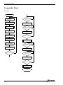
6. System Reference
Block Diagram
Interface Connector CH0
Receiver
Driver
UART
Device ID
XR16C2850
Compatible
Control Circuit
Stack Connector
Figure 6.1. Block Diagram
COM-1PD(FIT)GY
35
6. System Reference
Equivalence Circuit
SP491
100Ω
TxD, RTS
100Ω
RxD, CTS
47kΩ
6.2kΩ
6.2kΩ
47kΩ
Figure 6.2. Circuitry Diagrams RS-422A/485 in Full Duplex
SP491
TxD, RxD
47kΩ
6.2kΩ
100Ω
6.2kΩ
47kΩ
Figure 6.3. Circuitry Diagrams RS-422A/485 in Half Duplex
36
COM-1PD(FIT)GY
6. System Reference
Specification
Table 6.1. Specification
Item
Number of channels
Specification
1ch
Interface type
RS-422A/RS-485
Isolation
Bus Isolation
Isolation voltage
1000VDC
Transfer method
Asynchronous serial transfer (Full/Half duplex)
Baud rate
2 to 921,600bps *1 *2
Data length
5, 6, 7, 8 bits
Parity check
Even, Odd, Non-parity *1
Controller chip
162850 or equivalent
1, 1.5, 2 stop bits *1
(Each channel has 128-byte receive and 128-byte transmit FIFO buffers.)
Interrupt requests
1 level use
Power consumption
5VDC 300mA (Max.)
Connecting distance
Within 1200m *3
Dimension (mm)
25.2(W) x 64.7(D) x 94.0(H) (exclusive of protrusions)
Weight(module itself)
100g
Module connection method Stack connection by the connector that is provided woth the side of module
Module installation
One-touch connection to 35mm DIN rails.
method
(standard connection mechanism provided in the system)
*1
These items can be set by software.
*2
Data transmission at high speed may not be performed normally depending on the environment
including the type of status of connected material of cable and environment.
*3
The table below lists an example of the relationship between baud rate and communication distance.
Communication
Baud rate
distance
300m
115,200bps
600m
57,600bps
900m
19,200bps
1200m
9,600bps
Communication cable: 28AWG, double shielded cable, twisted pairs used for each +/- signal line.
CAUTION
When connecting the module to a controller module, the internal power consumption should be
taken into account. If the total current exceeds the capacity of the power supply unit, the integrity of
the operation cannot be guaranteed. For further details, please see the Controller Module manual.
COM-1PD(FIT)GY
37
6. System Reference
Table 6.2. Installation Environment Requirements
Parameter
Requirement description
Operating temperature
0 to 50°C
Storage temperature
-10 to 60°C
Humidity
10% to 90% (No condensation)
Floating dust particles
Not to be excessive
Corrosive gases
None
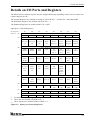
External Dimensions
(1.2)
14.0
(1.2)
CH0
TX
CD
F0 1 2
E
7 8 9A
6
RX
Device
ID
35.0
45.0
94.0
1 2 3 4 5 6 7 8 910
345
TERM
MODE
CH0
COM-1PD
3.5
25.2
64.7
4.0
[mm]
Figure 6.4. External Dimensions
38
COM-1PD(FIT)GY
COM-1PD(FIT)GY
User’s Manual
CONTEC CO., LTD.
December 2003 Edition
3-9-31, Himesato, Nishiyodogawa-ku, Osaka 555-0025, Japan
Japanese http://www.contec.co.jp/
English http://www.contec.com/
Chinese http://www.contec.com.cn/
No part of this document may be copied or reproduced in any form by any means without prior written
consent of CONTEC CO., LTD.
[08062003]
[12102003]
Management No. A-46-812
Parts No.
LYDC891